JP7308595B2 - image sensor - Google Patents
image sensor Download PDFInfo
- Publication number
- JP7308595B2 JP7308595B2 JP2018126170A JP2018126170A JP7308595B2 JP 7308595 B2 JP7308595 B2 JP 7308595B2 JP 2018126170 A JP2018126170 A JP 2018126170A JP 2018126170 A JP2018126170 A JP 2018126170A JP 7308595 B2 JP7308595 B2 JP 7308595B2
- Authority
- JP
- Japan
- Prior art keywords
- protective film
- photoelectric conversion
- image sensor
- film
- organic film
- Prior art date
- Legal status (The legal status is an assumption and is not a legal conclusion. Google has not performed a legal analysis and makes no representation as to the accuracy of the status listed.)
- Active
Links
- 230000001681 protective effect Effects 0.000 claims description 115
- 238000006243 chemical reaction Methods 0.000 claims description 26
- 239000000758 substrate Substances 0.000 claims description 11
- 238000001514 detection method Methods 0.000 claims description 6
- 239000011159 matrix material Substances 0.000 claims description 6
- 239000010408 film Substances 0.000 description 182
- 239000010410 layer Substances 0.000 description 40
- 239000004065 semiconductor Substances 0.000 description 20
- 229910021417 amorphous silicon Inorganic materials 0.000 description 9
- 239000000463 material Substances 0.000 description 9
- 230000003287 optical effect Effects 0.000 description 9
- 238000010586 diagram Methods 0.000 description 8
- 229910020286 SiOxNy Inorganic materials 0.000 description 5
- 238000003384 imaging method Methods 0.000 description 5
- 238000002161 passivation Methods 0.000 description 5
- 239000000470 constituent Substances 0.000 description 4
- 230000003071 parasitic effect Effects 0.000 description 4
- 230000002093 peripheral effect Effects 0.000 description 4
- PNEYBMLMFCGWSK-UHFFFAOYSA-N aluminium oxide Inorganic materials [O-2].[O-2].[O-2].[Al+3].[Al+3] PNEYBMLMFCGWSK-UHFFFAOYSA-N 0.000 description 3
- 229910052593 corundum Inorganic materials 0.000 description 3
- 238000002438 flame photometric detection Methods 0.000 description 3
- 238000004519 manufacturing process Methods 0.000 description 3
- 239000012044 organic layer Substances 0.000 description 3
- 229910001845 yogo sapphire Inorganic materials 0.000 description 3
- 239000004925 Acrylic resin Substances 0.000 description 2
- 229920000178 Acrylic resin Polymers 0.000 description 2
- 239000000853 adhesive Substances 0.000 description 2
- 230000001070 adhesive effect Effects 0.000 description 2
- 229910045601 alloy Inorganic materials 0.000 description 2
- 239000000956 alloy Substances 0.000 description 2
- 229910052782 aluminium Inorganic materials 0.000 description 2
- 239000003822 epoxy resin Substances 0.000 description 2
- 230000031700 light absorption Effects 0.000 description 2
- 229910052751 metal Inorganic materials 0.000 description 2
- 239000002184 metal Substances 0.000 description 2
- 238000000034 method Methods 0.000 description 2
- 239000005011 phenolic resin Substances 0.000 description 2
- 229910021420 polycrystalline silicon Inorganic materials 0.000 description 2
- 229920000647 polyepoxide Polymers 0.000 description 2
- 239000011347 resin Substances 0.000 description 2
- 229920005989 resin Polymers 0.000 description 2
- 229910004286 SiNxOy Inorganic materials 0.000 description 1
- 206010047571 Visual impairment Diseases 0.000 description 1
- 239000002390 adhesive tape Substances 0.000 description 1
- 230000002238 attenuated effect Effects 0.000 description 1
- 229910052804 chromium Inorganic materials 0.000 description 1
- 230000007797 corrosion Effects 0.000 description 1
- 238000005260 corrosion Methods 0.000 description 1
- 238000005336 cracking Methods 0.000 description 1
- 230000006866 deterioration Effects 0.000 description 1
- 229910052733 gallium Inorganic materials 0.000 description 1
- 239000011521 glass Substances 0.000 description 1
- 230000012447 hatching Effects 0.000 description 1
- 229910052738 indium Inorganic materials 0.000 description 1
- AMGQUBHHOARCQH-UHFFFAOYSA-N indium;oxotin Chemical compound [In].[Sn]=O AMGQUBHHOARCQH-UHFFFAOYSA-N 0.000 description 1
- 229910044991 metal oxide Inorganic materials 0.000 description 1
- 150000004706 metal oxides Chemical class 0.000 description 1
- 150000002739 metals Chemical class 0.000 description 1
- 229910052750 molybdenum Inorganic materials 0.000 description 1
- 229920000052 poly(p-xylylene) Polymers 0.000 description 1
- 239000011241 protective layer Substances 0.000 description 1
- 238000000926 separation method Methods 0.000 description 1
- 239000010409 thin film Substances 0.000 description 1
- 229910052718 tin Inorganic materials 0.000 description 1
- 229910052719 titanium Inorganic materials 0.000 description 1
- 229910052725 zinc Inorganic materials 0.000 description 1
Images


Classifications
-
- G—PHYSICS
- G01—MEASURING; TESTING
- G01T—MEASUREMENT OF NUCLEAR OR X-RADIATION
- G01T1/00—Measuring X-radiation, gamma radiation, corpuscular radiation, or cosmic radiation
- G01T1/16—Measuring radiation intensity
- G01T1/20—Measuring radiation intensity with scintillation detectors
-
- H—ELECTRICITY
- H01—ELECTRIC ELEMENTS
- H01L—SEMICONDUCTOR DEVICES NOT COVERED BY CLASS H10
- H01L27/00—Devices consisting of a plurality of semiconductor or other solid-state components formed in or on a common substrate
- H01L27/14—Devices consisting of a plurality of semiconductor or other solid-state components formed in or on a common substrate including semiconductor components sensitive to infrared radiation, light, electromagnetic radiation of shorter wavelength or corpuscular radiation and specially adapted either for the conversion of the energy of such radiation into electrical energy or for the control of electrical energy by such radiation
- H01L27/144—Devices controlled by radiation
- H01L27/146—Imager structures
- H01L27/14643—Photodiode arrays; MOS imagers
- H01L27/14658—X-ray, gamma-ray or corpuscular radiation imagers
- H01L27/14663—Indirect radiation imagers, e.g. using luminescent members
-
- H—ELECTRICITY
- H01—ELECTRIC ELEMENTS
- H01L—SEMICONDUCTOR DEVICES NOT COVERED BY CLASS H10
- H01L27/00—Devices consisting of a plurality of semiconductor or other solid-state components formed in or on a common substrate
- H01L27/14—Devices consisting of a plurality of semiconductor or other solid-state components formed in or on a common substrate including semiconductor components sensitive to infrared radiation, light, electromagnetic radiation of shorter wavelength or corpuscular radiation and specially adapted either for the conversion of the energy of such radiation into electrical energy or for the control of electrical energy by such radiation
- H01L27/144—Devices controlled by radiation
- H01L27/146—Imager structures
- H01L27/14601—Structural or functional details thereof
- H01L27/1462—Coatings
-
- G—PHYSICS
- G01—MEASURING; TESTING
- G01T—MEASUREMENT OF NUCLEAR OR X-RADIATION
- G01T1/00—Measuring X-radiation, gamma radiation, corpuscular radiation, or cosmic radiation
- G01T1/16—Measuring radiation intensity
- G01T1/20—Measuring radiation intensity with scintillation detectors
- G01T1/2002—Optical details, e.g. reflecting or diffusing layers
-
- G—PHYSICS
- G01—MEASURING; TESTING
- G01T—MEASUREMENT OF NUCLEAR OR X-RADIATION
- G01T1/00—Measuring X-radiation, gamma radiation, corpuscular radiation, or cosmic radiation
- G01T1/16—Measuring radiation intensity
- G01T1/20—Measuring radiation intensity with scintillation detectors
- G01T1/2018—Scintillation-photodiode combinations
- G01T1/20183—Arrangements for preventing or correcting crosstalk, e.g. optical or electrical arrangements for correcting crosstalk
-
- G—PHYSICS
- G01—MEASURING; TESTING
- G01T—MEASUREMENT OF NUCLEAR OR X-RADIATION
- G01T1/00—Measuring X-radiation, gamma radiation, corpuscular radiation, or cosmic radiation
- G01T1/16—Measuring radiation intensity
- G01T1/24—Measuring radiation intensity with semiconductor detectors
- G01T1/247—Detector read-out circuitry
-
- H—ELECTRICITY
- H01—ELECTRIC ELEMENTS
- H01L—SEMICONDUCTOR DEVICES NOT COVERED BY CLASS H10
- H01L27/00—Devices consisting of a plurality of semiconductor or other solid-state components formed in or on a common substrate
- H01L27/14—Devices consisting of a plurality of semiconductor or other solid-state components formed in or on a common substrate including semiconductor components sensitive to infrared radiation, light, electromagnetic radiation of shorter wavelength or corpuscular radiation and specially adapted either for the conversion of the energy of such radiation into electrical energy or for the control of electrical energy by such radiation
- H01L27/144—Devices controlled by radiation
- H01L27/146—Imager structures
- H01L27/14601—Structural or functional details thereof
- H01L27/14609—Pixel-elements with integrated switching, control, storage or amplification elements
- H01L27/14612—Pixel-elements with integrated switching, control, storage or amplification elements involving a transistor
-
- H—ELECTRICITY
- H01—ELECTRIC ELEMENTS
- H01L—SEMICONDUCTOR DEVICES NOT COVERED BY CLASS H10
- H01L27/00—Devices consisting of a plurality of semiconductor or other solid-state components formed in or on a common substrate
- H01L27/14—Devices consisting of a plurality of semiconductor or other solid-state components formed in or on a common substrate including semiconductor components sensitive to infrared radiation, light, electromagnetic radiation of shorter wavelength or corpuscular radiation and specially adapted either for the conversion of the energy of such radiation into electrical energy or for the control of electrical energy by such radiation
- H01L27/144—Devices controlled by radiation
- H01L27/146—Imager structures
- H01L27/14601—Structural or functional details thereof
- H01L27/1462—Coatings
- H01L27/14623—Optical shielding
-
- Y—GENERAL TAGGING OF NEW TECHNOLOGICAL DEVELOPMENTS; GENERAL TAGGING OF CROSS-SECTIONAL TECHNOLOGIES SPANNING OVER SEVERAL SECTIONS OF THE IPC; TECHNICAL SUBJECTS COVERED BY FORMER USPC CROSS-REFERENCE ART COLLECTIONS [XRACs] AND DIGESTS
- Y02—TECHNOLOGIES OR APPLICATIONS FOR MITIGATION OR ADAPTATION AGAINST CLIMATE CHANGE
- Y02E—REDUCTION OF GREENHOUSE GAS [GHG] EMISSIONS, RELATED TO ENERGY GENERATION, TRANSMISSION OR DISTRIBUTION
- Y02E10/00—Energy generation through renewable energy sources
- Y02E10/50—Photovoltaic [PV] energy
- Y02E10/549—Organic PV cells
Description
本開示は、イメージセンサに関する。 The present disclosure relates to image sensors.
間接型のX線撮像装置として、フラットパネルディテクタ(以下、Flat Panel Detector:FPDとも呼ぶ)が広く用いられている。FPDは、シンチレータと呼ばれるX線-光変換膜と、フォトダイオードアレイと、を含んで構成される。フォトダイオードアレイは、薄膜トランジスタ(Thin Film Transistor、以下TFTとも呼ぶ)とフォトダイオードとが接続して形成された受光素子を、マトリクス状に並べたデバイスである。フォトダイオードアレイは光をフォトダイオードで光電変換し、得られた電荷を、TFTを介して信号線から読み出して画像化する。 A flat panel detector (hereinafter also referred to as a Flat Panel Detector: FPD) is widely used as an indirect X-ray imaging apparatus. The FPD includes an X-ray-light converting film called a scintillator and a photodiode array. A photodiode array is a device in which light receiving elements formed by connecting thin film transistors (hereinafter also referred to as TFTs) and photodiodes are arranged in a matrix. In the photodiode array, the photodiodes photoelectrically convert light, and the obtained electric charges are read out from the signal line via the TFTs to form an image.
特許文献1はX線撮像装置を開示する。特許文献1に記載のX線撮像装置において、第2の絶縁膜は、第1の絶縁膜とフォトダイオード及び電極を含む変換素子を覆うように設けられている。また、特許文献1に記載の撮像パネルにおいて、第2の絶縁膜は、0より大きい数x及び0以上の数yに対して、SiNxOyで表される材料で形成されている。
高画質なFPD開発に向け、鮮鋭度の高い画像を得るニーズが高まっている。しかし、シンチレータからの光信号の進行方向が必ずしも受光面に対し垂直でないため、特許文献1に記載の技術では、本来入射すべき画素とは異なる画素(例えば、周辺画素)に光が入射してしまう可能性がある。つまり、この光は、周辺画素にとってはノイズ光(迷光)であるため、イメージセンサによって得られる画像がぼけてしまう、即ち鮮鋭度が低下してしまう。
There is a growing need to obtain high-definition images in order to develop high-quality FPDs. However, since the traveling direction of the optical signal from the scintillator is not necessarily perpendicular to the light-receiving surface, in the technique described in
また、特許文献1に記載の技術において、X線がシンチレータに対し垂直に入射しても、変換された光がイメージセンサの受光面(厳密には、特許文献1に記載の撮像パネルにおけるフォトダイオードの、特に非晶質シリコン層)に到達するまでに光学的な距離が存在するため、その間に光信号が散乱してしまい、一部の光信号が周辺画素に入射してしまう。つまり、鮮鋭度の高い画像を取得するには、各画素において周辺画素からのノイズ光の混入を抑制する必要がある。そこで本開示は、より鮮鋭度の高い画像を得ることを目的とする。
In addition, in the technique described in
上記課題を解決するために、本開示の一態様は以下の構成を採用する。イメージセンサは、基板上に配置されたスイッチング素子と、前記スイッチング素子に接続された光電変換素子と、前記光電変換素子を直接覆う第1保護膜と、前記スイッチング素子よりも上層に位置し、前記第1保護膜に接する第1有機膜と、を備え、前記第1有機膜は、前記光電変換素子の端部の少なくとも一部である第1端部を覆い、前記第1端部を覆う前記第1有機膜の端部である第1被覆部は、前記光電変換素子方向への傾斜を有して終端し、前記第1有機膜は、前記光電変換素子のうち前記第1端部のみを覆う、イメージセンサ。 In order to solve the above problems, one aspect of the present disclosure employs the following configuration. The image sensor comprises: a switching element arranged on a substrate; a photoelectric conversion element connected to the switching element; a first protective film directly covering the photoelectric conversion element; and a first organic film in contact with the first protective film, wherein the first organic film covers a first end that is at least part of the end of the photoelectric conversion element, and covers the first end. A first covering portion, which is an end portion of the first organic film, terminates with an inclination toward the photoelectric conversion element, and the first organic film covers only the first end portion of the photoelectric conversion element. Cover, image sensor.
本開示の一態様によれば、鮮鋭度の高い画像を得ることができる。 According to one aspect of the present disclosure, an image with high sharpness can be obtained.
以下、添付図面を参照して実施形態を説明する。本実施形態は本開示を実現するための一例に過ぎず、本開示の技術的範囲を限定するものではないことに注意すべきである。各図において共通の構成については同一の参照符号が付されている。また、図面に描かれた形状は、実際の寸法及び比率とは必ずしも一致しない。また、各図面におけるハッチングは、各構成要素を区別するためのものでもあり、必ずしも切断面を意味するものではない。また、説明をわかりやすくするため、図示した物の寸法、形状については、誇張して記載している場合もある。 Embodiments will be described below with reference to the accompanying drawings. It should be noted that the present embodiment is merely an example for realizing the present disclosure and does not limit the technical scope of the present disclosure. The same reference numerals are given to the common components in each figure. Also, the shapes depicted in the drawings do not necessarily match the actual dimensions and proportions. In addition, hatching in each drawing is also for distinguishing each component and does not necessarily mean a cut surface. In order to make the explanation easier to understand, the dimensions and shapes of the illustrated objects may be exaggerated.
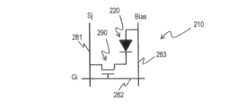
図1は、本実施例のイメージセンサの構成例を示すブロック図である。イメージセンサ10は、フォトダイオードアレイ200、走査回路400、及び検出回路300を含む。
FIG. 1 is a block diagram showing a configuration example of an image sensor of this embodiment.
フォトダイオードアレイ200において、縦方向に配置された信号線281(S1-Sm)と横方向に配置されたゲート線282(G1-Gn)との各交点に配置された画素210がマトリクス状に配置されている。信号線281(S1-Sm)は、それぞれ、異なる画素列に接続されている。ゲート線282(G1-Gn)は、それぞれ、異なる画素行に接続されている。
In the
また、図1には図示されていないが、イメージセンサ10は、後述するシンチレータ500を含む。シンチレータ500は、例えば、フォトダイオードアレイ200のZ軸方向にフォトダイオードアレイ200を覆うように配置されている。被写体に照射されたX線が被写体を透過してシンチレータ500に入射し、シンチレータ500は入射したX線を光に変換する。シンチレータ500が変換した光がフォトダイオードアレイ200に入射する。なお、イメージセンサ10は、シンチレータ500を含まなくてもよい。
Further, although not shown in FIG. 1, the
なお、本実施形態では、画素210が配列されたマトリクスの行方向及び列方向を、それぞれ、x軸方向、y軸方向とし、x軸及びy軸に直交し、フォトダイオードアレイ200にシンチレータ500が積層する方向をz軸方向とする。
In this embodiment, the row direction and column direction of the matrix in which the
センサ基板100は、絶縁性基板(例えばガラス基板)である。信号線281(S1-Sm)は検出回路300に接続され、ゲート線282(G1-Gn)は走査回路400に接続される。またここに示した例では、全ての画素210に共通のバイアス線283(Bias)が接続されているが、全ての画素210および共通のバイアス線283が複数の画素領域に分割されており、それぞれの画素領域に対応する独立したバイアス線およびバイアス端子が配置されていてもよい。
The
図2は、本実施例のイメージセンサ10に適用可能な画素210の回路構成例を示す回路図である。図2の画素210は、図1における上からi行目、左からj列目の画素210である。画素210は、フォトダイオード220とTFT290とを含む。フォトダイオード220は光電変換素子の一例である。TFT290は、スイッチング素子の一例である。なお、フォトダイオード220の代わりに、他の光電変換素子が用いられてもよい。また、TFT290の代わりに他のスイッチング素子が用いられてもよい。
FIG. 2 is a circuit diagram showing a circuit configuration example of the
TFT290のゲート端子はゲート線Giに接続され、ドレイン端子は信号線Sjに接続され、ソース端子はフォトダイオード220のカソード端子に接続される。図2の例において、フォトダイオード220のアノード端子は、バイアス線283(Bias)に接続されている。
The TFT 290 has a gate terminal connected to the gate line Gi, a drain terminal connected to the signal line Sj, and a source terminal connected to the cathode terminal of the
走査回路400は、フォトダイオードアレイ200における画素行を選択し、ゲート線282を介して、選択中の画素行の画素210に出力信号を出力してTFT290を導通状態にする。検出回路300は、導通状態のTFT290及び信号線281を介して、走査回路400が選択した画素行の画素210のフォトダイオード220からの信号を検出する。
The
続いて、図3乃至図5を用いてフォトダイオードアレイ200の概略について説明する。説明の便宜のため、図3乃至図5にはフォトダイオードアレイ200の一部の構成の記載を省略する場合もある。例えば、図3には、後述する第2保護膜250、第3保護膜260、及び第2有機膜270等が記載されていない。
Next, an outline of the
図3は、フォトダイオードアレイ200の上面の一例を示す概略図である。フォトダイオードアレイ200は、フォトダイオード220、第1有機膜230、第1保護膜240、及び第2保護膜250を含む。前述したように、フォトダイオードアレイ200において、フォトダイオード220がマトリクス状に配置されている。また、第1有機膜230が、フォトダイオード220間の隙間を埋めるように、井桁状に配置されている。
FIG. 3 is a schematic diagram showing an example of the top surface of the
図4は、図3のA-A’線で切断したフォトダイオードアレイ200の断面の一例を示す概略図である。フォトダイオード220それぞれは、下部に配置された下部電極221を含む。下部電極221の端部221aは、フォトダイオード220の下部電極221を除く部分における端部220a(以下、単にフォトダイオード220の端部220aとも呼ぶ)の外側に位置する。第1保護膜240それぞれは、フォトダイオード220を直接覆うように積層している。
FIG. 4 is a schematic diagram showing an example of a cross section of the
第1有機膜230は、隣接する第1保護膜240の間に配置される。具体的には、例えば、第1有機膜230は、隣接する第1保護膜240の間を満たす。第1有機膜230の端部230aは、フォトダイオード220の端部220aの内側に位置する。また、第1有機膜230の端部230aは、z軸の負の方向(即ちフォトダイオード220が存在する方向)に傾斜している。
The first
なお、フォトダイオード220の上面における端部220a(外周)の少なくとも一部の直上(z軸の正の方向)に、第1有機膜230の端部230aが位置すればよい。図3の例では、フォトダイオード220のxy平面における端部220a(外周)全体の内側に、第1有機膜230の端部230aが位置する。なお、フォトダイオード220の上面の少なくとも一部の直上には、第1有機膜230が存在しない。
Note that the
図3及び図4の例では、フォトダイオード220の上面の中央部の直上には、第1有機膜230が存在しない。なお、z軸方向において第1有機膜230とフォトダイオード220とが重複する部分の面積は、z軸方向において第1有機膜230と重複しないフォトダイオード220の部分の面積より十分小さいことが望ましい。
In the examples of FIGS. 3 and 4, the first
第1有機膜230及び第1保護膜240を直接覆うように第2保護膜250が積層している。従って、フォトダイオード220の上面の直上に第1有機膜230が存在しない部分においては、第2保護膜250は、第1保護膜240上に積層している。
A second
なお、第2保護膜250は、第1有機膜230及び第1保護膜240の形状をなぞるように積層しているため、第1有機膜230の端部230aの直上で、z軸の負の方向(即ちフォトダイオード220が存在する方向)に傾斜している。なお、フォトダイオードアレイ200は、第2保護膜250を含む方が望ましいが、含まなくてもよい。
In addition, since the second
第1有機膜230は、例えば、アクリル樹脂、フェノール樹脂、又はエポキシ樹脂等の有機樹脂材料で構成される。第1保護膜240及び第2保護膜250は、例えば、SiOxNy(x,yは0又は任意の自然数)等の絶縁性無機膜で構成される。
The first
図5は、図4のA部の一例を示す部分拡大図である。図5における入射光601及び入射光602の光路において、第2保護膜250がある場合、第2保護膜250は、第2保護膜250に入射する直前の他の媒質と比較して、高屈折率である。第2保護膜250がない場合、第1有機膜230の端部230aには後述する第3保護膜260(この場合、第3保護膜260は第2保護膜250と光学的に同様の機能を果たす)が直上に位置するので、第3保護膜260は、前記第3保護膜260に入射する直前の他の媒質と比較して、高屈折率である。
FIG. 5 is a partially enlarged view showing an example of part A in FIG. In the optical paths of the
第2保護膜250及び第3保護膜260がともにない場合、第1有機膜230の端部230aは、前記端部230aに入射する直前の他の媒質と比較して、高屈折率である。なお第2保護膜250、第3保護膜260、又は端部230aに光が入射する直前に他の材質の層がない場合は、他の媒質とは空気(屈折率1.0)を指すものとする。
In the absence of both the second
図4の第1有機膜230と、無機膜である第1保護膜240、及び無機膜である第2保護膜250又は第3保護膜260と(但し、図4及び後述する図5においては第2保護膜250として記載)、の間の熱膨張率差が大きい。一方、第1保護膜240と、第2保護膜250又は第3保護膜260と、の間の熱膨張率差は小さい。フォトダイオード220の上面の中央部の直上には、第1有機膜230が存在せず、第1保護膜240と、第2保護膜250又は第3保護膜260と、が積層している。
The first
つまり、フォトダイオード220の上面の中央部の直上においては、第1保護膜240の上に熱膨張率差が小さい第2保護膜250又は第3保護膜260が直接積層しているため、製造プロセスにおける温度差の影響を受けにくい。その結果、第1保護膜240と、第2保護膜250又は第3保護膜260と、の間の剥離やそれぞれの膜の亀裂が生じにくい。従って、フォトダイオードアレイ200の耐湿性が向上し、ひいてはフォトダイオードアレイ200の信頼性が向上する。
That is, immediately above the central portion of the upper surface of the
また、第1保護膜240と、第2保護膜250又は第3保護膜260と、が同一又は類似する材質であるため、第1保護膜240の上に第2保護膜250又は第3保護膜260が直接積層している部分において、第1保護膜240と、第2保護膜250又は第3保護膜260と、の密着性が高い。従って、当該部分において膜浮きや膜剥がれが生じにくくなり、ひいては画像のムラが発生しにくくなる。
In addition, since the first
また、第1有機膜230は、xy平面において、最も外側に位置するフォトダイオード220の外側にも配置されているが、最も外側に位置するフォトダイオード220より外側に位置する第1有機膜230の端部230bも、第2保護膜250又は第3保護膜260によって密封されている。従って、端部230bからの水分の侵入を防ぐことができる。これにより、フォトダイオードアレイ200の配線の腐食、並びにフォトダイオード220及びTFT290の特性悪化を抑制することができる。なお、フォトダイオードアレイ200のy軸方向の端部においても、第1有機膜230が、第2保護膜250又は第3保護膜260によって密封されている。
In addition, the first
図5に記載されたフォトダイオード220を他のフォトダイオード220と区別するためにフォトダイオード220-1と呼ぶ。入射光601及び入射光602は、いずれもシンチレータ500からフォトダイオードアレイ200に入射する光である。一般にシンチレータの発する光の波長は可視光であり、例えばシンチレータの一種であるCsI:Tlは、中心波長が550nm程度である。
The
入射光601は、フォトダイオード220-1に入射すべき光成分(例えば、シンチレータ500のフォトダイオード220-1の直上に配置された部分から入射した光)を多く含む。入射光602は、フォトダイオード220-1に入射すべきでない光成分(例えば、シンチレータ500のフォトダイオード220-1の直上以外に配置された部分から入射した光、即ち他のフォトダイオード220(例えば隣接する画素210等の周辺画素のフォトダイオード220)に入射すべき光)を多く含む。
入射光601のほとんどの光成分は、フォトダイオード220-1にそのまま入射する。一方、入射光602に含まれる入射すべきでない光成分は、例えば隣接する画素210の直上のシンチレータ500の部分から入射しているため、入射角が大きく、さらにフォトダイオード220-1の端部220-1aの直上の近傍から入射しやすい。また、前述したように、第2保護膜250又は第3保護膜260に入射する直前の他の媒質の屈折率と比較して、第2保護膜250又は第3保護膜260の屈折率が高い。
Most of the light components of the
従って、入射光602の少なくとも一部は、第2保護膜250又は第3保護膜260、及び第1有機膜230に設けられた傾斜部分において屈折し、フォトダイオード220-1に入射しない。これにより、各画素210において隣接する画素210からの光の混入を抑制することができる。その結果、隣接する画素210からの光によって引き起こされていた、画像のぼやけを改善し鮮鋭度を向上させることができる。
Therefore, at least part of the
なお、第1有機膜230は、例えば、380nm~700nmの波長範囲で光吸収特性を有してもよい。入射光602に含まれる入射光602-1は、第1有機膜230に設けられた傾斜部分において屈折するものの、第1有機膜230を通過して、フォトダイオード220-1に入射する。第1有機膜230が当該光吸収特性を有することにより、フォトダイオード220に入射する入射光602-1の光強度が第1有機膜230によって減衰するため、画像の鮮鋭度がさらに向上する。
Note that the first
以下、図6乃至図8を用いて、フォトダイオードアレイ200の構成の詳細を説明する。図6は、図3のB部(第1有機膜230を非表示)の一例を示す部分拡大図である。図7は、図3のB部(第1有機膜230を表示)の一例を示す部分拡大図である。図8は、図6のA-A’線で切断したフォトダイオードアレイ200の断面の第1の例を示す断面図である。なお、図8には、フォトダイオードアレイ200を覆うシンチレータ500、及びフォトダイオードアレイ200の直下に配置されるセンサ基板100も描かれている。また、図8には、後述する第2保護膜250、第3保護膜260、及び第2有機膜270等についても描かれている。
The details of the configuration of the
センサ基板100上にTFT290が配置されている。TFT290は、ゲート電極291、ゲート絶縁膜292、半導体層293、ソース電極294、及びドレイン電極295を含む。センサ基板100上にゲート電極291が配置され、ゲート電極291を直接覆うようにセンサ基板100上にゲート絶縁膜292が積層している。
A
ゲート電極291の直上に、ゲート絶縁膜292を介して、半導体層293が配置されている。また、ソース電極294及びドレイン電極295が、ゲート絶縁膜292上に配置されている。半導体層293のx軸方向の正の方向の端部にソース電極294が接続されている。半導体層293のx軸の負の方向の端部にドレイン電極295が接続されている。ソース電極294とドレイン電極295とは隔離されている。
A
なお、ゲート電極291の構成材料は、例えば、Al、Cr、又はこれらの金属の合金などである。ゲート絶縁膜292の構成材料は、例えば、SiOxNy(x,yは0又は任意の自然数)、Al2O3及びそれらの積層膜などである。半導体層293は、例えば、a-Si(アモルファスシリコン)若しくはpoly-Si(多結晶シリコン)、又はIn、Ga、Zn、及びSnなどの金属酸化物などで構成される。ドレイン電極295の構成材料は、例えば、AlとMo及びTiなどの合金などの、抵抗率の低い金属である。
The constituent material of the
なお、ゲート電極291の厚さ(以下、特に断らない限り、「厚さ」とは、z軸方向の厚さを示す)は、例えば、100~1000nm程度である。ゲート絶縁膜292の厚さは、例えば、200~600nm程度である。半導体層293の厚さは、例えば、10~500nm程度である。ソース電極294及びドレイン電極295の厚さは、例えば、100~1000nm程度である。
Note that the thickness of the gate electrode 291 (hereinafter, “thickness” indicates the thickness in the z-axis direction unless otherwise specified) is, for example, about 100 to 1000 nm. The thickness of the
半導体層293、ソース電極294、及びドレイン電極295を覆うように、TFT保護膜280が積層している。TFT保護膜280は、例えば、SiOxNy(x,yは0又は任意の自然数)やAl2O3等の絶縁性無機膜で構成される。TFT保護膜280の厚さは、100~2000nm程度である。
A TFT
TFT保護膜280上にフォトダイオード220及び第1有機膜230が配置される。第1有機膜230の厚さは、例えば、500~2500nm程度である。フォトダイオード220は、例えば、z軸の負の方向から順に、下部電極221、n型a-Si層222、i型a-Si層223、p型a-Si層224、上部電極225、が積層されることによって構成される。
A
下部電極221は、TFT保護膜280を貫通して、例えば第1コンタクト部285において、ソース電極294に接続される。下部電極221には、例えば、Crなどを用いることができる。上部電極225の構成材料は、例えば、ITO(Indium Tin Oxide)などの透明電極を用いることができる。下部電極221の厚さは、例えば、10~200nm程度である。上部電極225の厚さは、例えば、10~200nm程度である。
The
n型a-Si層222の厚さは、例えば、10~100nm程度である。i型a-Si層223の厚さは、例えば、500~2000nm程度である。p型a-Si層224の厚さは、例えば、10~100nm程度である。
The thickness of the n-
また、TFT290とフォトダイオード220との間の寄生容量を低減するために、図8のように、TFT290とフォトダイオード220が離間して配置されていることが好ましい。同様に、フォトダイオード220間の寄生容量を低減するために、フォトダイオード220についても離間して配置されていることが好ましい。
In order to reduce the parasitic capacitance between the
第1保護膜240は、フォトダイオード220を直接覆う。また、第1有機膜230は、隣接する第1保護膜240の間に配置される。前述した通り、第1有機膜230及び第1保護膜240を直接覆うように、第2保護膜250が積層している。第1保護膜240の厚さは、例えば、50~2000nm程度である。第2保護膜250の厚さは、例えば、50~1000nm程度である。なお、第2保護膜250は、第1有機膜230及び第1保護膜240の形状をなぞるように積層しているため、第1有機膜230の端部230aの直上で、z軸の負の方向に傾斜している。
The
また、前述したように第1有機膜230の端部230aは、フォトダイオード220の端部220aの内側に位置し、第1有機膜230の端部220aは、z軸の負の方向(即ちフォトダイオード220が存在する方向)に傾斜している。
In addition, as described above, the
第1有機膜230とフォトダイオード220とが重なる幅L1は、10μm以下が望ましく、例えば、3μmである。フォトダイオード220の幅L2は、200μm以下であり、用途によっては100μm以下である。また、L1は、L2より十分小さい。また、第1有機膜230の端部220aの傾斜角は、例えば、15度~75度程度である。
A width L1 where the first
また、上部電極225上に、バイアス線283が配置されている。バイアス線283は、第1保護膜240及び第2保護膜250を貫通して、例えば第2コンタクト部286において、上部電極225に接続されている。また、ドレイン電極295上に、信号線281が配置されている。
A
信号線281は、第2保護膜250を貫通して、例えば第3コンタクト部287において、ドレイン電極295に接続されている。また、第1有機膜230と信号線281との間は、第2保護膜250によって隔てられている。
The
なお、第1有機膜230は比誘電率が低く、また、信号線281と、TFT290及びフォトダイオード220と、の間の空間の大半は、第1有機膜230で満たされていることが望ましい。これにより、信号線281の寄生容量を低減することができる。信号線281の寄生容量が低下することにより、検出回路300は信号を高速に読み取ることができるため、イメージセンサ10の残像特性が改善する。
It is desirable that the first
図6乃至図8の例では、信号線281及びバイアス線283の少なくとも一部が、第1有機膜230より上層に位置しているが、信号線281及びバイアス線283の全体が第1有機膜230より上層に位置しなくてもよい。
6 to 8, at least part of the
ゲート線282は、例えば、図6のフォトダイオード220の場合はy軸の負の方向に位置し、x軸方向に沿って配置されている。ゲート線282は、例えば、zx平面と平行な平面において、ゲート電極291に接続されている。信号線281、ゲート線282、及びバイアス線283の厚さは、例えば、100~1000nm程度である。
The
信号線281、及びバイアス線283を直接覆うように第3保護膜260が積層している。第3保護膜260は、例えば、SiOxNy(x,yは0又は任意の自然数)等の絶縁性無機膜で構成される。第3保護膜260は、信号線281及びバイアス線283を保護する。なお、第3保護膜260は、第2保護膜250の形状をなぞるように積層しているため、第1有機膜230の端部230aの直上で、z軸の負の方向に傾斜している。なお、第3保護膜260はある方が望ましいが、なくてもよい。
A third
第3保護膜260を覆うように第2有機膜270が積層している。第2有機膜270は、例えば、アクリル樹脂、フェノール樹脂、エポキシ樹脂等の有機樹脂材料の平坦化膜や、パリレンなどに代表されるシンチレータ保護膜、光学両面テープ(OCAテープ:Optical Clear Adhesive tape)や光学接着剤などに代表されるシンチレータ接着剤などが該当する。第2有機膜270を覆うようにシンチレータ500が配置される。
A second
なお、第3保護膜260の厚さは、例えば、50~1000nm程度である。第2有機膜270の厚さは、例えば、500~5000nmである。シンチレータ500の厚さは、例えば、10nm~10mm程度である。なお、フォトダイオードアレイ200は、第3保護膜260及び第2有機膜270の少なくとも一方を含まなくてもよい。
Note that the thickness of the third
図9は、図6のA-A’線で切断したフォトダイオードアレイ200の断面の第2の例を示す断面図である。図8との相違点を説明する。図8の例では、TFT290の形状が逆スタガ型であったが、図9の例では、TFT290の形状が順スタガ型である。順スタガ型と逆スタガ型の最大の違いは、半導体層293とゲート電極291の位置関係の違いである。
FIG. 9 is a cross-sectional view showing a second example of a cross section of the
センサ基板100上に半導体層293、ソース電極294、及びドレイン電極295が配置されている。半導体層293のx軸方向の正の方向の端部にソース電極294が接続されている。半導体層293のx軸の負の方向の端部にドレイン電極295が接続されている。
A
半導体層293、ソース電極294、及びドレイン電極295を覆うようにゲート絶縁膜292が積層している。半導体層293の直上に、ゲート絶縁膜292を介して、ゲート電極291が配置されている。ゲート電極291を覆うように、TFT保護膜280が積層している。
A
図10は、図6のA-A’線で切断したフォトダイオードアレイ200の断面の第3の例を示す断面図である。図8との相違点を説明する。図10の例では、半導体層293と、ソース電極294及びドレイン電極295と、の接続がチャネルエッチ型である。半導体層293の上面のx軸方向(又はy軸方向)の中央部が窪んでいる。
FIG. 10 is a cross-sectional view showing a third example of a cross section of the
図11は、図6のA-A’線で切断したフォトダイオードアレイ200の断面の第4の例を示す断面図である。図8との相違点を説明する。図11の例では、半導体層293と、ソース電極294及びドレイン電極295と、の接続がチャネル保護型である。TFT290は、エッチストップ層296をさらに含む。
FIG. 11 is a cross-sectional view showing a fourth example of a cross section of the
半導体層293のx軸方向(又はy軸方向)の中央部に、島状のエッチストップ層296が配置されている。エッチストップ層296の正のx軸方向の端部にソース電極294が接している。エッチストップ層296の負のx軸方向の端部にドレイン電極295が接している。エッチストップ層296は、例えば、SiOxNy(x,yは0又は任意の自然数)やAl2O3等の絶縁性無機膜で構成される。エッチストップ層296の厚さは、例えば、10~500nm程度である。
An island-shaped
図12は、図6のA-A’線で切断したフォトダイオードアレイ200の断面の第5の例を示す断面図である。図11との相違点を説明する。図12の例では、半導体層293と、ソース電極294及びドレイン電極295と、の接続がコンタクト型である。
FIG. 12 is a cross-sectional view showing a fifth example of a cross section of the
半導体層293を覆うように、エッチストップ層296が積層されている。エッチストップ層296上に、ソース電極294及びドレイン電極295が配置されている。また、ソース電極294及びドレイン電極295は、エッチストップ層296を貫通して、半導体層293に接続される。
An
図13は、図6のA-A’線で切断したフォトダイオードアレイ200の断面の第6の例を示す断面図である。図8との相違点を説明する。図8の例では、互いに隔離された第1保護膜240が、フォトダイオード220それぞれを覆う。
FIG. 13 is a cross-sectional view showing a sixth example of a cross section of the
一方、図13の例では、一連の第1保護膜240が全てのフォトダイオード220を覆うように積層している。即ち、図13の例においては、図4における第1保護膜240同士が繋がっている。第1保護膜240が一連の形状を有することにより、フォトダイオードアレイ200の製造工程において、フォトダイオード220を覆わない部分を除去する工程が不要であるため、製造効率が高まる。
On the other hand, in the example of FIG. 13, a series of first
図14は、図6のA-A’線で切断したフォトダイオードアレイ200の断面の第7の例を示す断面図である。図14の断面図は、フォトダイオードアレイ200が、第2保護膜250を含まない点を除いて、図8と同様である。
FIG. 14 is a cross-sectional view showing a seventh example of a cross section of the
図15は、図6のA-A’線で切断したフォトダイオードアレイ200の断面の第8の例を示す断面図である。図15の断面図は、フォトダイオードアレイ200が、第2保護膜250及び第3保護膜260を含まない点を除いて、図8と同様である。
FIG. 15 is a cross-sectional view showing an eighth example of the cross section of the
以上、本発明の実施形態を説明したが、本発明が上記の実施形態に限定されるものではない。例えば、図2に示した画素210の回路構成として、フォトダイオード220のアノード端子、カソード端子が、各々、TFT290、及びバイアス線283に接続されてもよい。このように、当業者であれば、上記の実施形態の各要素を、本発明の範囲において容易に変更、追加、変換することが可能である。ある実施形態の構成の一部を他の実施形態の構成に置き換えることが可能であり、ある実施形態の構成に他の実施形態の構成を加えることも可能である。
Although the embodiments of the present invention have been described above, the present invention is not limited to the above embodiments. For example, as the circuit configuration of the
10 イメージセンサ、100 センサ基板、200 フォトダイオードアレイ、210 画素、220 フォトダイオード、221 下部電極、230 第1有機膜、240 第1保護膜、250 第2保護膜、260 第3保護膜、270 第2有機膜、280 TFT保護膜、290 TFT、281 信号線、282 ゲート線、283 バイアス線、300 検出回路、400 走査回路、500 シンチレータ 10 image sensor, 100 sensor substrate, 200 photodiode array, 210 pixel, 220 photodiode, 221 lower electrode, 230 first organic film, 240 first protective film, 250 second protective film, 260 third protective film, 270 third 2 organic film, 280 TFT protective film, 290 TFT, 281 signal line, 282 gate line, 283 bias line, 300 detection circuit, 400 scanning circuit, 500 scintillator
Claims (6)
前記スイッチング素子に接続された光電変換素子と、
前記光電変換素子を直接覆う第1保護膜と、
前記スイッチング素子よりも上層に位置し、前記第1保護膜に接する第1有機膜と、を備え、
前記第1有機膜は、前記光電変換素子の端面を含む前記光電変換素子の部位、である第1端部を覆い、
前記第1端部を覆う前記第1有機膜の端部である第1被覆部は、前記光電変換素子方向への傾斜を有して終端し、
前記第1有機膜は、前記光電変換素子のうち前記第1端部のみを覆う、イメージセンサであって、
前記第1有機膜を直接覆う第2保護膜と、
前記第1有機膜及び前記第2保護膜よりも上層に位置する配線を直接覆う第3保護膜と、を備え、
前記第1保護膜、前記第2保護膜、及び前記第3保護膜は無機膜であり、
前記第3保護膜は前記第2保護膜を直接覆い、
前記第2保護膜は前記第1保護膜を直接覆い、
前記第2保護膜の前記第1被覆部を直接覆う部分は、前記光電変換素子方向への傾斜を有する、イメージセンサ。 a switching element arranged on the substrate;
a photoelectric conversion element connected to the switching element;
a first protective film that directly covers the photoelectric conversion element;
a first organic film located above the switching element and in contact with the first protective film;
The first organic film covers a first end portion, which is a portion of the photoelectric conversion element including the end face of the photoelectric conversion element,
a first covering portion, which is an end portion of the first organic film covering the first end portion, terminates with an inclination toward the photoelectric conversion element;
The image sensor, wherein the first organic film covers only the first end of the photoelectric conversion element ,
a second protective film directly covering the first organic film;
a third protective film that directly covers wiring positioned above the first organic film and the second protective film;
the first protective film, the second protective film, and the third protective film are inorganic films;
the third protective film directly covering the second protective film;
the second protective film directly covering the first protective film;
The image sensor, wherein a portion of the second protective film that directly covers the first covering portion has an inclination toward the photoelectric conversion element.
マトリクス状に配置された複数の画素を含み、 including a plurality of pixels arranged in a matrix,
前記複数の画素それぞれは、前記スイッチング素子と、前記光電変換素子と、を含み、 each of the plurality of pixels includes the switching element and the photoelectric conversion element;
前記第1有機膜は、前記光電変換素子の間、及び前記複数の画素において最も外側に位置する光電変換素子である最外光電変換素子の外側に配置され、 The first organic film is arranged between the photoelectric conversion elements and outside the outermost photoelectric conversion element, which is the outermost photoelectric conversion element in the plurality of pixels,
前記最外光電変換素子の外側に位置する前記第1有機膜の端部は、前記第2保護膜で直接覆われている、イメージセンサ。 The image sensor, wherein an end portion of the first organic film located outside the outermost photoelectric conversion element is directly covered with the second protective film.
前記第1有機膜よりも上層に第2有機膜を備える、イメージセンサ。 An image sensor comprising a second organic film above the first organic film.
複数の前記光電変換素子を備え、 comprising a plurality of said photoelectric conversion elements,
1つの前記第1保護膜が、前記複数の光電変換素子の全てを直接覆う、イメージセンサ。 The image sensor, wherein one of the first protective films directly covers all of the plurality of photoelectric conversion elements.
マトリクス状に配置された複数の画素を含み、 including a plurality of pixels arranged in a matrix,
前記複数の画素それぞれは、前記スイッチング素子と、前記光電変換素子と、を含み、 each of the plurality of pixels includes the switching element and the photoelectric conversion element;
前記イメージセンサは、 The image sensor is
前記スイッチング素子に接続されたゲート線及び信号線と、 a gate line and a signal line connected to the switching element;
行方向に配置された画素からなる画素行を選択し、前記ゲート線を介して、前記選択中の画素行の画素に出力信号を出力して前記スイッチング素子を導通状態にする、走査部と、 a scanning unit that selects a pixel row composed of pixels arranged in a row direction and outputs an output signal to the pixels in the selected pixel row through the gate line to turn on the switching element;
前記選択中の画素行の画素の光電変換素子からの信号を、導通状態の前記スイッチング素子及び前記信号線を介して検出する、検出部と、を備え、 a detection unit that detects a signal from the photoelectric conversion element of the pixel in the selected pixel row via the switching element in a conductive state and the signal line;
前記信号線は、前記第1有機膜を介して、前記光電変換素子と隔てられている、イメージセンサ。 The image sensor, wherein the signal line is separated from the photoelectric conversion element via the first organic film.
前記スイッチング素子を覆うスイッチング素子保護膜を備え、 A switching element protective film covering the switching element,
前記光電変換素子及び前記第1有機膜は、前記スイッチング素子保護膜上に配置されている、イメージセンサ。 The image sensor, wherein the photoelectric conversion element and the first organic film are arranged on the switching element protective film.
Priority Applications (3)
| Application Number | Priority Date | Filing Date | Title |
|---|---|---|---|
| JP2018126170A JP7308595B2 (en) | 2018-07-02 | 2018-07-02 | image sensor |
| CN201910542833.3A CN110676270A (en) | 2018-07-02 | 2019-06-21 | Image sensor with a plurality of pixels |
| US16/459,792 US10914846B2 (en) | 2018-07-02 | 2019-07-02 | Image sensor |
Applications Claiming Priority (1)
| Application Number | Priority Date | Filing Date | Title |
|---|---|---|---|
| JP2018126170A JP7308595B2 (en) | 2018-07-02 | 2018-07-02 | image sensor |
Publications (3)
| Publication Number | Publication Date |
|---|---|
| JP2020004935A JP2020004935A (en) | 2020-01-09 |
| JP2020004935A5 JP2020004935A5 (en) | 2021-08-05 |
| JP7308595B2 true JP7308595B2 (en) | 2023-07-14 |
Family
ID=69008066
Family Applications (1)
| Application Number | Title | Priority Date | Filing Date |
|---|---|---|---|
| JP2018126170A Active JP7308595B2 (en) | 2018-07-02 | 2018-07-02 | image sensor |
Country Status (3)
| Country | Link |
|---|---|
| US (1) | US10914846B2 (en) |
| JP (1) | JP7308595B2 (en) |
| CN (1) | CN110676270A (en) |
Families Citing this family (4)
| Publication number | Priority date | Publication date | Assignee | Title |
|---|---|---|---|---|
| KR102569741B1 (en) * | 2018-10-31 | 2023-08-22 | 엘지디스플레이 주식회사 | Thin film transistor array substrate digital x-ray detector and digital x-ray detector including the same |
| CN111508986A (en) * | 2020-04-29 | 2020-08-07 | Tcl华星光电技术有限公司 | Sensor, manufacturing method thereof and photoelectric conversion device |
| CN115702500A (en) * | 2020-06-08 | 2023-02-14 | 罗姆股份有限公司 | Semiconductor device and electronic apparatus |
| US11804503B2 (en) * | 2020-06-12 | 2023-10-31 | Sharp Kabushiki Kaisha | Photoelectric conversion device and x-ray imaging device |
Citations (10)
| Publication number | Priority date | Publication date | Assignee | Title |
|---|---|---|---|---|
| JP2010245078A (en) | 2009-04-01 | 2010-10-28 | Epson Imaging Devices Corp | Photoelectric conversion device and x-ray imaging device |
| JP2014078651A (en) | 2012-10-12 | 2014-05-01 | Nlt Technologies Ltd | Photoelectric conversion device, method of manufacturing the same, and x-ray image detector |
| JP2014116429A (en) | 2012-12-07 | 2014-06-26 | Japan Display Inc | Image-capturing device and image display system |
| JP2015090957A (en) | 2013-11-07 | 2015-05-11 | Nltテクノロジー株式会社 | Image sensor and manufacturing method therefor |
| JP2015144298A (en) | 2015-03-04 | 2015-08-06 | キヤノン株式会社 | Manufacturing method of semiconductor device |
| WO2015146855A1 (en) | 2014-03-28 | 2015-10-01 | 富士フイルム株式会社 | Radiation-detecting device and method for manufacturing radiation-detecting device |
| WO2016002563A1 (en) | 2014-06-30 | 2016-01-07 | シャープ株式会社 | Imaging panel and x-ray imaging device |
| WO2016195000A1 (en) | 2015-06-04 | 2016-12-08 | シャープ株式会社 | Photosensor substrate |
| WO2018056255A1 (en) | 2016-09-21 | 2018-03-29 | シャープ株式会社 | Imaging panel and method for producing same |
| WO2018070349A1 (en) | 2016-10-11 | 2018-04-19 | シャープ株式会社 | Imaging panel and manufacturing method therefor |
Family Cites Families (6)
| Publication number | Priority date | Publication date | Assignee | Title |
|---|---|---|---|---|
| US6465824B1 (en) * | 2000-03-09 | 2002-10-15 | General Electric Company | Imager structure |
| TW201403804A (en) * | 2012-07-05 | 2014-01-16 | Sony Corp | Solid-state imaging device, method for manufacturing same, and electronic device |
| JP2014081358A (en) * | 2012-09-27 | 2014-05-08 | Fujifilm Corp | Radiation image detector |
| JP2015012239A (en) * | 2013-07-01 | 2015-01-19 | ソニー株式会社 | Imaging element and electronic device |
| JP2018084485A (en) * | 2016-11-24 | 2018-05-31 | コニカミノルタ株式会社 | Radiation image taking device |
| KR102506885B1 (en) * | 2018-02-27 | 2023-03-06 | 삼성전자주식회사 | Image sensor |
-
2018
- 2018-07-02 JP JP2018126170A patent/JP7308595B2/en active Active
-
2019
- 2019-06-21 CN CN201910542833.3A patent/CN110676270A/en active Pending
- 2019-07-02 US US16/459,792 patent/US10914846B2/en active Active
Patent Citations (10)
| Publication number | Priority date | Publication date | Assignee | Title |
|---|---|---|---|---|
| JP2010245078A (en) | 2009-04-01 | 2010-10-28 | Epson Imaging Devices Corp | Photoelectric conversion device and x-ray imaging device |
| JP2014078651A (en) | 2012-10-12 | 2014-05-01 | Nlt Technologies Ltd | Photoelectric conversion device, method of manufacturing the same, and x-ray image detector |
| JP2014116429A (en) | 2012-12-07 | 2014-06-26 | Japan Display Inc | Image-capturing device and image display system |
| JP2015090957A (en) | 2013-11-07 | 2015-05-11 | Nltテクノロジー株式会社 | Image sensor and manufacturing method therefor |
| WO2015146855A1 (en) | 2014-03-28 | 2015-10-01 | 富士フイルム株式会社 | Radiation-detecting device and method for manufacturing radiation-detecting device |
| WO2016002563A1 (en) | 2014-06-30 | 2016-01-07 | シャープ株式会社 | Imaging panel and x-ray imaging device |
| JP2015144298A (en) | 2015-03-04 | 2015-08-06 | キヤノン株式会社 | Manufacturing method of semiconductor device |
| WO2016195000A1 (en) | 2015-06-04 | 2016-12-08 | シャープ株式会社 | Photosensor substrate |
| WO2018056255A1 (en) | 2016-09-21 | 2018-03-29 | シャープ株式会社 | Imaging panel and method for producing same |
| WO2018070349A1 (en) | 2016-10-11 | 2018-04-19 | シャープ株式会社 | Imaging panel and manufacturing method therefor |
Also Published As
| Publication number | Publication date |
|---|---|
| US20200003911A1 (en) | 2020-01-02 |
| JP2020004935A (en) | 2020-01-09 |
| CN110676270A (en) | 2020-01-10 |
| US10914846B2 (en) | 2021-02-09 |
Similar Documents
| Publication | Publication Date | Title |
|---|---|---|
| JP7308595B2 (en) | image sensor | |
| US9806123B2 (en) | Image sensor and manufacturing method thereof | |
| US11309451B2 (en) | Flat panel detector and manufacturing method thereof | |
| US8803210B2 (en) | X-ray detector | |
| US20100054418A1 (en) | X-ray detecting element | |
| US8039809B2 (en) | Sensor panel and image detecting device | |
| US8916833B2 (en) | Imaging device and imaging display system | |
| US9299737B2 (en) | Image pickup device, method of manufacturing the same, and image pickup display system | |
| KR102517730B1 (en) | Digital x-ray detector panel and the x-ray system including the same | |
| KR102583562B1 (en) | Array substrate for digital x-ray detector, x-ray detector including the same | |
| US20210135020A1 (en) | Detection panel, manufacturing method thereof and detection device | |
| US20120248318A1 (en) | Radiographic image-pickup device and radiographic image-pickup display system | |
| US20130048860A1 (en) | Photoelectric conversion substrate, radiation detector, and radiographic image capture device | |
| JP2013157347A (en) | Imaging device and method of manufacturing the same, and imaging display system | |
| JP2008277710A (en) | Light receiving element and display unit equipped with the same | |
| JP2009272452A (en) | Solid-state imaging device | |
| US10705230B2 (en) | Imaging panel | |
| KR102651991B1 (en) | The digital x-ray detector and the manufacturing method thereof | |
| US20170221939A1 (en) | Functional element and electronic apparatus | |
| KR102619971B1 (en) | Digital x-ray detector and method of fabricating thereof | |
| US20230387151A1 (en) | Image sensor | |
| US11705532B2 (en) | X-ray device | |
| US20220299663A1 (en) | Detection substrate, method for manufacturing the same and flat panel detector | |
| KR102631651B1 (en) | Digital x-ray detector having improved fill factor | |
| KR101858356B1 (en) | Digital x-ray detector for blocking hydrogen |
Legal Events
| Date | Code | Title | Description |
|---|---|---|---|
| A521 | Request for written amendment filed |
Free format text: JAPANESE INTERMEDIATE CODE: A523 Effective date: 20210628 |
|
| A621 | Written request for application examination |
Free format text: JAPANESE INTERMEDIATE CODE: A621 Effective date: 20210628 |
|
| A977 | Report on retrieval |
Free format text: JAPANESE INTERMEDIATE CODE: A971007 Effective date: 20220712 |
|
| A131 | Notification of reasons for refusal |
Free format text: JAPANESE INTERMEDIATE CODE: A131 Effective date: 20220719 |
|
| A521 | Request for written amendment filed |
Free format text: JAPANESE INTERMEDIATE CODE: A523 Effective date: 20220916 |
|
| A131 | Notification of reasons for refusal |
Free format text: JAPANESE INTERMEDIATE CODE: A131 Effective date: 20230110 |
|
| A521 | Request for written amendment filed |
Free format text: JAPANESE INTERMEDIATE CODE: A523 Effective date: 20230228 |
|
| TRDD | Decision of grant or rejection written | ||
| A01 | Written decision to grant a patent or to grant a registration (utility model) |
Free format text: JAPANESE INTERMEDIATE CODE: A01 Effective date: 20230627 |
|
| A61 | First payment of annual fees (during grant procedure) |
Free format text: JAPANESE INTERMEDIATE CODE: A61 Effective date: 20230704 |
|
| R150 | Certificate of patent or registration of utility model |
Ref document number: 7308595 Country of ref document: JP Free format text: JAPANESE INTERMEDIATE CODE: R150 |