JP7307601B2 - Microfluidic device - Google Patents
Microfluidic device Download PDFInfo
- Publication number
- JP7307601B2 JP7307601B2 JP2019114044A JP2019114044A JP7307601B2 JP 7307601 B2 JP7307601 B2 JP 7307601B2 JP 2019114044 A JP2019114044 A JP 2019114044A JP 2019114044 A JP2019114044 A JP 2019114044A JP 7307601 B2 JP7307601 B2 JP 7307601B2
- Authority
- JP
- Japan
- Prior art keywords
- resin substrate
- bonding
- bonding region
- microchannel
- microfluidic device
- Prior art date
- Legal status (The legal status is an assumption and is not a legal conclusion. Google has not performed a legal analysis and makes no representation as to the accuracy of the status listed.)
- Active
Links
Images


Description
本発明は、積層させた2枚の基板の対向する接合面間を接合し、その間にマイクロ流路が形成されるマイクロ流路デバイスに関する。 TECHNICAL FIELD The present invention relates to a microfluidic device in which the facing joint surfaces of two laminated substrates are joined to form a microfluidic channel therebetween.
マイクロ流路デバイスは、2枚の積層する基板間に幅500nm乃至1mm程度の微細なマイクロ流路が形成されたデバイスであり、マイクロ流路に連通する注入孔から有機化合物、生体試料などの微量の試料をマイクロ流路に注入し、試料を混合、反応、合成、抽出、分析する等の用途で用いられている。 A microfluidic device is a device in which a fine microfluidic channel with a width of about 500 nm to 1 mm is formed between two laminated substrates, and a trace amount of an organic compound, a biological sample, etc. is injected from an injection hole communicating with the microfluidic channel. It is used for purposes such as injecting a sample into a microchannel and mixing, reacting, synthesizing, extracting, and analyzing the sample.
マイクロ流路の形状や大きさは、マイクロ流路に注入する試料についてのこれらの用途の判定に影響しないように高精度に製造されるが、基板の接合面間を接合する際に、気泡が残っていたり、加熱接合や接着剤の収縮等の影響で、接合した2枚の基板が湾曲し、マイクロ流路も変形するという問題があった。 The shape and size of the microchannel are manufactured with high precision so as not to affect the determination of the use of the sample injected into the microchannel. There is a problem that the two substrates that are joined are curved and the microchannel is also deformed due to the influence of heat joining, shrinkage of the adhesive, or the like.
また、2枚の積層する基板の間に形成されるマイクロ流路の形状や数は、マイクロ流路デバイスの用途に応じて任意に設計されるが、基板間の2次元平面内という制約を受けるので、近年は、それぞれ2枚の積層する基板の間にマイクロ流路を形成した複数のマイクロ流路チップを、積層方向に多段に重ね、積層方向で重ねられるマイクロ流路チップのマイクロ流路間を、積層方向に基板を貫通させた貫通孔を介して連通し、マイクロ流路を3次元の立体形状で形成するマイクロ流路デバイスが検討されている。 In addition, the shape and number of microchannels formed between two stacked substrates can be arbitrarily designed according to the application of the microchannel device, but they are restricted to being within a two-dimensional plane between the substrates. Therefore, in recent years, a plurality of microchannel chips in which microchannels are formed between two stacked substrates are stacked in multiple stages in the stacking direction, and the microchannel chips stacked in the stacking direction are communicated with each other through through-holes penetrating through the substrate in the lamination direction to form a three-dimensional microchannel device.
このマイクロ流路デバイスでは、各マイクロ流路チップを構成する基板がわずかに湾曲しても、多段に重ねることによって湾曲する変位が累積されて全体で大きく湾曲したり、水平面に沿ってマイクロ流路チップを多段に重ねることが困難となっていた。 In this microfluidic device, even if the substrates constituting each microfluidic chip are slightly curved, the bending displacement accumulated by stacking them in multiple stages causes the entirety to be largely curved, or the microfluidic device to bend along the horizontal plane. It has been difficult to stack chips in multiple stages.
そこで、マイクロ流路が形成される基板や、接合面の間にマイクロ流路を形成して接合される2枚の積層する基板の湾曲や反りを防止する種々の方法が提案されている。このうち、特許文献1のマイクロ流路デバイスは、積層する2枚の基板の接合面に基板を溶解しない揮発性液体を介在させて接合面に残る空気を揮発させ、その後、揮発性液体を除去した基板間を密着し、加熱及び加圧により接合している。従って、接合面間に残留する気泡によって接合する基板が湾曲することがない。
Therefore, various methods have been proposed to prevent the substrates on which the microchannels are formed, or two stacked substrates that are joined by forming the microchannels between the bonding surfaces, from bending or warping. Among them, in the microfluidic device of
また、特許文献2のマイクロ流路デバイスは、一方の基板の接合面のマイクロ流路に沿った周囲に微小突起を形成し、微小突起の部分と対向する接合面との間を超音波溶着により接合する。これにより、2枚の基板の対向する接合面間に空気が残留していても、微小突起の部分で接合するので、気泡が残留することによるマイクロ流路の変形や基板の反りを防止できる。
Further, in the microfluidic device of
また、特許文献3のマイクロ流路デバイスは、マイクロ流路が形成されていない接合面の一部にマイクロ流路として使用しないダミー流路を形成する。接合面にダミー流路が形成されるので、成形金型から離型しやすくなり、離型の際に発生する基板の反りが防止される。
Further, in the microfluidic device of
また、特許文献4のマイクロ流路デバイスは、第1基板の可変形温度を第2基板の可変形温度より高い材質とし、積層させた第1基板と第2基板をそれぞれの加熱変形温度の間で加熱し、湾曲する張り合わせ面の一方に合わせて他方の張り合わせ面が追従して密着するように湾曲させる。
In addition, in the microfluidic device of
また、特許文献5のマイクロ流路デバイスは、樹脂製フィルムが接合する基板の接合面より側方に突出する出っ張り部を基板の側面に形成し、基板の接合面に樹脂フィルムを加熱接合する際に、出っ張り部を冶具で押さえつけて、基板の反りを抑える。
Further, in the microfluidic device of
特許文献1のマイクロ流路デバイスは、基板間を接合する前に、揮発性液体を接合面に付着させる必要があり、また、基板の一部が変形している場合には、その変形による隙間の空気は除去することができない。また、特許文献2のマイクロ流路デバイスは、微小突起の部分でのみ接合するので、接合強度が弱く、更に、特許文献1と特許文献2に記載のいずれのマイクロ流路デバイスも、基板自体に応力が発生することによる湾曲や反りを防止するものではなく、基板の一部が湾曲していると、基板の接合面の隙間からマイクロ流路に注入する試料が漏れ出す恐れがある。
In the microfluidic device of
また、特許文献3では、ダミー流路を形成することと、金型からの離型が容易で基板の反りが防止されるとの因果関係が必ずしも明確ではないが、多数のダミー流路が同一方向に形成されているだけなので、基板の接合面間に残留する気泡や、接合工程において基板に発生する応力によって各方向に発生する恐れのある基板の湾曲や反りを防止することはできない。
Further, in
また、特許文献4のマイクロ流路デバイスは、接合する2枚の基板の材料に加熱変形温度の異なる材料とする制約があるとともに、変形した一枚の基板に対して他方の基板を合わせるので、マイクロ流路は湾曲した基板に沿って形成され、特許文献5のマイクロ流路デバイスは、基板の各方向への反りを防止するために、基板の4カ所の各側面に出っ張り部を設ける必要があり、基板間を接合する工程で、基板を平坦面に維持する冶具が必要となるので、いずれも実用的ではない。
Further, in the microfluidic device of
更に、2枚の基板の接合前に、2枚の基板の対向する接合面の間に潤滑液を介在させ、2枚の基板間のスライドを容易にして、2枚の基板を相対位置決めしているが、潤滑液が気化するまでは、接合させることができず、生産スループット低下の原因となっていた。 Furthermore, before joining the two substrates, a lubricating liquid is interposed between the opposing joining surfaces of the two substrates to facilitate sliding between the two substrates and position the two substrates relative to each other. However, until the lubricating liquid evaporates, it cannot be joined, causing a decrease in production throughput.
本発明は、このような従来の問題点を考慮してなされたものであり、2枚の基板の接合面の間に気泡が残留していたり、基板を接合する工程において基板の一部に応力が発生しても、接合した2枚以上の多段流路基板が湾曲したり、反りが生じることがないマイクロ流路デバイスを提供することを目的とする。 The present invention has been made in consideration of such conventional problems. An object of the present invention is to provide a microchannel device in which two or more multistage channel substrates joined together are not bent or warped even when a crack occurs.
また、2枚の積層する基板のいずれかに簡単な加工を加えるだけで、接合した2枚の基板の平面性を維持できるマイクロ流路デバイスを提供することを目的とする。 It is another object of the present invention to provide a microfluidic device capable of maintaining the planarity of two bonded substrates simply by applying a simple process to one of the two laminated substrates.
また、潤滑液を用いて接合する2枚の基板間の位置決めを行っても、短時間に接合工程を行うことができるマイクロ流路デバイスを提供することを目的とする。 Another object of the present invention is to provide a microfluidic device in which the bonding process can be performed in a short time even if the two substrates to be bonded are positioned using a lubricating liquid.
上述の目的を達成するため、請求項1に記載のマイクロ流路デバイスは、表面にマイクロ流路が凹設された平板状の第1樹脂基板と、第1樹脂基板の表面上に積層される第2樹脂基板を備え、第1樹脂基板の表面のマイクロ流路が凹設された部位を除く第1接合領域と、第1接合領域に積層方向で対向する第2樹脂基板の第2接合領域が一体に接合されるマイクロ流路デバイスであって、
第1接合領域と第2接合領域のいずれか一方若しくは双方の接合面のマイクロ流路が凹設された部位に接しない接合領域に、凹溝若しくはスリットからなる応力緩和部が格子状に形成されていることを特徴とする。
In order to achieve the above object, the microfluidic device according to
In one or both of the bonding surfaces of the first bonding region and the second bonding region, a stress relief portion composed of grooves or slits is formed in a grid pattern in the bonding region that is not in contact with the portion where the microchannel is recessed. It is characterized by
第1接合領域と第2接合領域の接合面の間に気泡が残留していたり、第1接合領域と第2接合領域の接合面を接合する工程に起因して、接合する第1接合領域と第2接合領域の一部に接合面に沿った応力が発生しても、接合面に形成される凹溝若しくはスリットからなる応力緩和部において応力による歪が吸収され、部分的に発生した応力は、応力緩和部を越えて伝達されず、接合する第1樹脂基板と第2樹脂基板の全体に湾曲や反りは生じない。 Air bubbles remain between the joint surfaces of the first joint region and the second joint region, or due to the process of joining the joint surfaces of the first joint region and the second joint region, the first joint region to be joined Even if stress is generated along the joint surface in a part of the second joint region, the strain due to the stress is absorbed in the stress relaxation part consisting of the groove or slit formed in the joint surface, and the partially generated stress is reduced. , the stress is not transmitted beyond the stress relaxation portion, and the first resin substrate and the second resin substrate to be bonded do not bend or warp as a whole.
応力緩和部は、接合面に格子状に形成されているので、接合面に沿っていずれの方向の応力が発生しても、応力緩和部を超えて伝達されず、接合する第1樹脂基板と第2樹脂基板はいずれの方向にも湾曲しない。 Since the stress relief portion is formed in a grid pattern on the bonding surface, even if stress is generated in any direction along the bonding surface, it is not transmitted beyond the stress relief portion, and the first resin substrate to be bonded is not transmitted. The second resin substrate does not bend in any direction.
請求項2に記載のマイクロ流路デバイスは、接合面に応力緩和部が形成される第1樹脂基板若しくは第2樹脂基板は、PDMS(ポリジメチルシロキサン)で成形され、第1接合領域と第2接合領域の双方の接合面を表面改質して、第1接合領域と第2接合領域が一体に接合されることを特徴とする。
In the microfluidic device according to
接合する第1樹脂基板と第2樹脂基板の少なくとも一方が、エラストマーであるPDMSで成形されるので、一方の接合領域にわずかな湾曲部があっても、対向する他方の接合領域と密着し、表面改質してむらなく一体に接合できる。 Since at least one of the first resin substrate and the second resin substrate to be bonded is molded with PDMS, which is an elastomer, even if one bonding region has a slight curved portion, it is in close contact with the opposing bonding region, It can be joined integrally by modifying the surface.
また、応力緩和部は、エラストマーであるPDMSで成形される第1樹脂基板若しくは第2樹脂基板に形成されるので、応力緩和部において接合面に沿った大きい伸縮変位が吸収される。 In addition, since the stress relaxation part is formed on the first resin substrate or the second resin substrate formed of PDMS, which is an elastomer, a large expansion/contraction displacement along the bonding surface is absorbed in the stress relaxation part.
また、マイクロ流路を囲う第1樹脂基板若しくは第2樹脂基板のいずれかが、半透明あるいは透明材料であるPDMSを成形材料として成形されるので、マイクロ流路へ注入する試料の色や量を目視確認できる。 In addition, since either the first resin substrate or the second resin substrate surrounding the microchannel is molded using PDMS, which is a translucent or transparent material, as a molding material, the color and amount of the sample to be injected into the microchannel can be controlled. Visual confirmation is possible.
請求項3に記載のマイクロ流路デバイスは、第1樹脂基板が、PDMS(ポリジメチルシロキサン)を成形材料として成形され、応力緩和部は、第1接合領域の接合面に形成される凹溝からなることを特徴とする。
In the microfluidic device according to
マイクロ流路が凹設される第1樹脂基板の表面と同一面に応力緩和部が形成されるので、マイクロ流路を形成する金型の成形面を加工するだけで、格子状の応力緩和部が形成される。 Since the stress relaxation part is formed on the same surface as the surface of the first resin substrate in which the microchannel is recessed, the lattice-like stress relaxation part can be obtained only by processing the molding surface of the mold for forming the microchannel. is formed.
マイクロ流路と応力緩和部が形成される第1樹脂基板が、金型の成形面への転写性にすぐれたPDMSを成形材料として成形されるので、微細なマイクロ流路と応力緩和部を高精度に第1接合領域の接合面に形成できる。 Since the first resin substrate on which the microchannel and the stress relaxation part are formed is molded using PDMS, which has excellent transferability to the molding surface of the mold, the fine microchannel and the stress relaxation part can be formed at a high level. It can be accurately formed on the joint surface of the first joint region.
請求項4に記載のマイクロ流路デバイスは、マイクロ流路と凹溝の第1接合領域の接合面からの深さが同一であることを特徴とする。
The microchannel device according to
フォトリソグラフィー技術によるレジストエッチングあるいは電鋳工法により、マイクロ流路と凹溝を形成する同一高さの突部を有する型が容易に得られる。 A mold having projections of the same height for forming microchannels and grooves can be easily obtained by resist etching using photolithography or electroforming.
請求項5に記載のマイクロ流路デバイスは、応力緩和部が、接合する第1樹脂基板と第2樹脂基板の側面に開口する凹溝からなることを特徴とする。 According to a fifth aspect of the microfluidic device, the stress relieving portion is composed of a concave groove that opens to side surfaces of the first resin substrate and the second resin substrate to be bonded.
第1接合領域と第2接合領域を接合する際にその間に残される気泡は、周囲の凹溝を通して凹溝の開口から外部に排出され、第1接合領域と第2接合領域の接合面間に残留する気泡が圧縮されることよる応力は発生しない。 Air bubbles left between the first joint region and the second joint region when the first joint region and the second joint region are joined are discharged to the outside from the opening of the concave groove through the surrounding concave groove, and are discharged between the joint surfaces of the first joint region and the second joint region. There is no stress due to compression of residual air bubbles.
請求項6に記載のマイクロ流路デバイスは、それぞれ第1樹脂基板と第2樹脂基板を積層してなる複数のマイクロ流路チップが、積層方向に多段に積層されて一体に接合され、多段に積層された各マイクロ流路チップに形成されるマイクロ流路間は、第1樹脂基板若しくは第2樹脂基板を積層方向に貫通する貫通孔を介して連通するとともに、積層方向で対向するマイクロ流路チップの第1接合領域と第2接合領域の一方若しくは双方の接合面に、凹溝若しくはスリットからなる応力緩和部が格子状に形成されていることを特徴とする。
In the microfluidic device according to
第1樹脂基板と第2樹脂基板の間にマイクロ流路が形成されるマイクロ流路チップが多段に重ねられ、各マイクロ流路チップに形成されるマイクロ流路間が貫通孔を介して連通するので、3次元の立体形状でマイクロ流路を形成できる。 Microchannel chips in which microchannels are formed between a first resin substrate and a second resin substrate are stacked in multiple stages, and the microchannels formed in each microchannel chip communicate with each other through through holes. Therefore, a microchannel can be formed in a three-dimensional shape.
多段に重ねられる各マイクロ流路チップの接合面に部分的に発生する応力は、応力緩和部を越えて伝達されず、接合するマイクロ流路チップの全体に湾曲や反りが生じないので多段に重ねることができ、また多段に重ねても、各マイクロ流路は水平面に沿って形成される。 The stress generated partially on the bonding surface of each microchannel chip stacked in multiple stages is not transmitted beyond the stress relief portion, and the entirety of the microchannel chips to be bonded does not bend or warp. Each microchannel is formed along the horizontal plane even if the microchannels are stacked in multiple stages.
請求項7に記載のマイクロ流路デバイスは、表面にマイクロ流路が凹設された平板状の第1樹脂基板と、第1樹脂基板の表面上に積層される第2樹脂基板を備え、第1樹脂基板の表面のマイクロ流路が凹設された部位を除く第1接合領域と、第1接合領域に積層方向で対向する第2樹脂基板の第2接合領域が一体に接合されるマイクロ流路デバイスであって、
第1接合領域と第2接合領域のいずれか一方若しくは双方の接合面のマイクロ流路が凹設された部位に接しない接合領域の全体に、接合する第1樹脂基板と第2樹脂基板の側面に開口する多数の凹溝が形成されていることを特徴とする。
A microfluidic device according to
The side surfaces of the first resin substrate and the second resin substrate that are bonded to the entire bonding region that is not in contact with the portion in which the microchannel is recessed on either or both of the bonding surfaces of the first bonding region and the second bonding region characterized in that a large number of concave grooves are formed that open to the
第1樹脂基板と第2樹脂基板を接合する前に、2枚の基板の対向する接合面の間に潤滑液を介在させ、2枚の基板間のスライドを容易にして相対位置決めしても、潤滑液は、凹溝に流れて接合面に残留せず、また、外部に開口して通気する凹溝内で早期に気化する。 Prior to bonding the first resin substrate and the second resin substrate, lubricating liquid is interposed between the facing bonding surfaces of the two substrates to facilitate sliding between the two substrates for relative positioning. The lubricating liquid flows into the grooves and does not remain on the joint surface, and vaporizes quickly in the grooves that open to the outside for ventilation.
第1接合領域と第2接合領域の接合面の間に気泡が残留していたり、第1接合領域と第2接合領域の接合面を接合する工程に起因して、接合面に沿って凹溝に交差する方向の応力が発生しても、その応力による歪は凹溝で吸収され、凹溝を超えて伝達されず、接合する第1樹脂基板と第2樹脂基板の湾曲が緩和される。 Air bubbles remain between the joint surfaces of the first joint region and the second joint region, or due to the process of joining the joint surfaces of the first joint region and the second joint region, concave grooves along the joint surfaces Even if a stress is generated in a direction crossing the two, the distortion due to the stress is absorbed by the groove and is not transmitted beyond the groove, thereby relaxing the curvature of the first resin substrate and the second resin substrate to be bonded.
請求項8に記載のマイクロ流路デバイスは、第1樹脂基板と第2樹脂基板の少なくとも一方は、PDMS(ポリジメチルシロキサン)で成形され、第1接合領域と第2接合領域の双方の接合面を表面改質して、第1接合領域と第2接合領域が一体に接合されることを特徴とする。
In the microfluidic device according to
PDMS(ポリジメチルシロキサン)の自己吸着性により密着する第1樹脂基板と第2樹脂基板の接合面間に潤滑液を介在させることにより、2枚の基板間のスライドを容易にして相対位置決めすることができる。接合面間に介在させた潤滑液は、凹溝に流れて接合面に残留せず、また、外部に開口して通気する凹溝内で早期に気化する。 By interposing a lubricating liquid between the bonding surfaces of the first resin substrate and the second resin substrate that are in close contact with each other due to the self-adsorption property of PDMS (polydimethylsiloxane), the two substrates can be easily slid and positioned relative to each other. can be done. The lubricating liquid interposed between the joint surfaces flows into the grooves and does not remain on the joint surfaces, and is quickly vaporized in the grooves open to the outside for ventilation.
請求項9に記載のマイクロ流路デバイスは、凹溝が、第1接合領域の接合面に形成され、マイクロ流路と凹溝の第1接合領域の接合面からの深さが同一であることを特徴とする。 In the microfluidic device according to claim 9, the concave groove is formed on the bonding surface of the first bonding region, and the microchannel and the concave groove have the same depth from the bonding surface of the first bonding region. characterized by
フォトリソグラフィー技術によるレジストエッチングあるいは電鋳工法により、マイクロ流路と凹溝を形成する同一高さの突部を有する型が容易に得られる。 A mold having projections of the same height for forming microchannels and grooves can be easily obtained by resist etching using photolithography or electroforming.
請求項10に記載のマイクロ流路デバイスは、それぞれ第1樹脂基板と第2樹脂基板を積層してなる複数のマイクロ流路チップが、積層方向に多段に積層されて一体に接合され、多段に積層された各マイクロ流路チップに形成されるマイクロ流路間は、第1樹脂基板若しくは第2樹脂基板を積層方向に貫通する貫通孔を介して連通するとともに、積層方向で対向するマイクロ流路チップの第1接合領域と第2接合領域の一方若しくは双方の接合面の全体に、接合する第1樹脂基板と第2樹脂基板の側面に開口する多数の凹溝が形成されていることを特徴とする
In the microfluidic device according to
多段に重ねられた各マイクロ流路チップの2枚の基板の対向する接合面の間に潤滑液を介在させ、全てのマイクロ流路間が貫通孔を介して連通するように、積層される多数の第1樹脂基板と第2樹脂基板を同時にスライドさせて相対位置決めしても、潤滑液は、各接合面に形成される凹溝に流れて接合面に残留せず、また、外部に開口して通気する凹溝内で早期に気化する。 Lubricating liquid is interposed between the facing joint surfaces of the two substrates of each microchannel chip stacked in multiple stages, and a large number of microchannel chips are stacked so that all the microchannels communicate with each other through the through holes. Even if the first resin substrate and the second resin substrate are slid at the same time and positioned relative to each other, the lubricating liquid flows into the concave grooves formed on the respective bonding surfaces and does not remain on the bonding surfaces, and is opened to the outside. evaporates quickly in grooves vented by
請求項1の発明によれば、2枚の接合させる樹脂基板の間に気泡が残留していたり、樹脂基板の接合面を接合する工程において、接合面の一部に応力が発生しても、接合面に格子状に形成する応力緩和部を越えて応力が伝達されないので、接合した2枚の樹脂基板を平坦にできる。従って、2枚の樹脂基板の間に形成されるマイクロ流路を、その一部が傾斜したり、内径が変化することがなく、高精度に形成できる。 According to the first aspect of the invention, even if air bubbles remain between two resin substrates to be bonded or stress is generated in a part of the bonding surfaces in the process of bonding the bonding surfaces of the resin substrates, Since the stress is not transmitted beyond the stress relief portion formed in a grid pattern on the bonding surface, the bonded two resin substrates can be flattened. Therefore, the microchannel formed between the two resin substrates can be formed with high precision without a part thereof being inclined or the inner diameter thereof being changed.
請求項2の発明によれば、接合する第1樹脂基板と第2樹脂基板の少なくとも一方が、エラストマーであるPDMSで成形されるので、第1接合領域若しくは第2接合領域に部分的に大きな応力が生じても、接合する第1接合領域と第2接合領域の全体を平坦に維持できる。
According to the invention of
また、接合する第1樹脂基板と第2樹脂基板の接合面を表面改質して接合するので、第1接合領域と第2接合領域がむらなく一体に接合され、第1接合領域と第2接合領域の隙間からマイクロ流路に注入した試料が漏れ出ない。 In addition, since the bonding surfaces of the first resin substrate and the second resin substrate to be bonded are bonded after surface modification, the first bonding region and the second bonding region are evenly and integrally bonded. The sample injected into the microchannel does not leak out from the gap in the joint region.
請求項3の発明によれば、マイクロ流路を形成する型の成形面に加工を加えるだけで、格子状の応力緩和部を形成できる。 According to the third aspect of the invention, the grid-like stress relief portion can be formed simply by processing the molding surface of the mold for forming the microchannel.
また、微細なマイクロ流路と応力緩和部とを高精度に接合面に形成できる。 Also, fine microchannels and stress relief portions can be formed on the joint surface with high accuracy.
請求項4と請求項9の発明によれば、マイクロ流路と格子状の応力緩和部の凹溝を、高精度の成形が可能な電鋳の金型あるいはフォトリソグラフィー技術によるレジストエッチング型で成形することができる。
According to the inventions of
請求項5の発明によれば、接合する第1接合領域と第2接合領域の接合面間に気泡が残留することがなく、残留する気泡が圧縮されることよる応力が接合面に発生しない。
According to the invention of
請求項6の発明によれば、第1樹脂基板と第2樹脂基板を積層したマイクロ流路チップを多段に重ねて、マイクロ流路を立体形状で設計でき、また、マイクロ流路チップを多段に重ねても、各マイクロ流路チップのマイクロ流路は水平面に沿って形成される。
According to the invention of
請求項7の発明によれば、第1樹脂基板と第2樹脂基板間の接合面間の摩擦を減じて2枚の基板間の相対位置決めを容易にするするために、接合面に潤滑液を介在させても、潤滑液は早期に気化し、若しくは凹溝に収容されて接合面に残らないので、相対位置決め後に、早期に第1樹脂基板と第2樹脂基板間を接合できる。 According to the seventh aspect of the invention, lubricating liquid is applied to the joint surfaces in order to reduce the friction between the joint surfaces of the first resin substrate and the second resin substrate and facilitate the relative positioning between the two substrates. Even if it is interposed, the lubricating liquid quickly evaporates or is contained in the concave groove and does not remain on the bonding surface, so that the first resin substrate and the second resin substrate can be quickly bonded after the relative positioning.
また、2枚の接合させる樹脂基板の間に気泡が残留していたり、樹脂基板の接合面を接合する工程において、接合面の一部に応力が発生しても、接合面に形成する凹溝を越えて応力による歪が伝達されないので、接合した2枚の樹脂基板を平坦に近づけることができる。 In addition, even if air bubbles remain between the two resin substrates to be bonded or stress is generated in a part of the bonding surfaces in the process of bonding the bonding surfaces of the resin substrates, the concave grooves formed on the bonding surfaces Since the strain due to the stress is not transmitted beyond the , the two bonded resin substrates can be flattened.
請求項8の発明によれば、少なくとも一方の接合面が自己吸着性を有するPDMSであって、密着する接合面間のスライドを容易にするために潤滑液を介在させても、スライドさせて相対位置決めした後の接合面間に潤滑液が残留しないので、表面改質した接合面間を早期に接合できる。 According to the eighth aspect of the invention, at least one joint surface is made of PDMS having self-adsorbing property, and even if a lubricating liquid is interposed to facilitate sliding between the closely contacting joint surfaces, it is possible to slide them relative to each other. Since the lubricating liquid does not remain between the joint surfaces after positioning, the surface-modified joint surfaces can be quickly joined.
また、接合する第1樹脂基板と第2樹脂基板の少なくとも一方が、エラストマーであるPDMSで成形されるので、第1接合領域若しくは第2接合領域に部分的に大きな応力が生じても、接合する第1接合領域と第2接合領域の全体を平坦に維持できる。 In addition, since at least one of the first resin substrate and the second resin substrate to be bonded is molded with PDMS, which is an elastomer, even if a large stress is locally generated in the first bonding region or the second bonding region, the bonding can be performed. The whole of the first bonding area and the second bonding area can be kept flat.
また、第1樹脂基板と第2樹脂基板の接合面を表面改質して接合するので、第1接合領域と第2接合領域がむらなく一体に接合され、第1接合領域と第2接合領域の隙間からマイクロ流路に注入した試料が漏れ出ない。 In addition, since the bonding surfaces of the first resin substrate and the second resin substrate are surface-modified and bonded, the first bonding region and the second bonding region are evenly and integrally bonded, and the first bonding region and the second bonding region are bonded together. The sample injected into the microchannel does not leak out from the gap between the
請求項10の発明によれば、潤滑液を用いて、多段に積層された各マイクロ流路チップの第1樹脂基板と第2樹脂基板を同時にスライドさせて相対位置決めしても、潤滑液が各接合面間に残らず、多段に積層された全てのマイクロ流路チップ間を早期に一体に接合できる。
According to the invention of
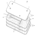
以下、本発明の第1実施の形態に係るマイクロ流路デバイス1を、図1乃至図7を用いて説明する。このマイクロ流路デバイス1は、積層する2枚の樹脂基板であるベースシート2とカバーシート3とから構成され、ベースシート2とカバーシート3を積層することにより、その間に形成されるマイクロ流路5に有機化合物、生体試料などの微量の試料を注入し、マイクロ流路5内に注入される試料を混合、反応、合成、抽出、分離、若しくは分析する用途で使用される。
A
ベースシート2は、PDMS(ポリジメチルシロキサン)を成形材料として、後述する電鋳の金型を用いたインジェクション成形で全体が薄肉の平板状に形成され、図4乃至図6に示すように、その表面(カバーシート3との対向面)に、幅及び深さが500nm乃至1mmのマイクロ流路5を形成する凹部5aと、凹部5aと同一深さの応力緩和部となる多数の凹溝4が形成されている。マイクロ流路5を形成する凹部5aは、マイクロ流路デバイス1の用途に応じて、その長さや形状、本数が任意に設計され、凹部5aの一端は、後述する注入孔6や排出孔7にマイクロ流路5に連通させるために凹部5aの幅より長い内径の円筒形となっている。また、応力緩和部となる多数の凹溝4は、直交する2方向に沿った多数の凹溝4が、ベースシート2の表面のマイクロ流路5を形成する凹部5aの形成部位を除く第1接合領域2Aの全域に、それぞれ交差して格子状にむらなく形成される。
The
ベースシート2を金型で成形する成形材料を、金型内で流動性の高いPDMSとするので、金型の成形面への転写性にすぐれ、微小なマイクロ流路5を形成する凹部5aや凹溝4をベースシート2の表面に高精度に形成できる。
Since the molding material for molding the
本実施の形態において、ベースシート2の表面に凹設するマイクロ流路5を形成する凹部5aや応力緩和部となる凹溝4を同一の深さとするので、微細なマイクロ流路5を形成する凹部5aや凹溝4を高精度に成形可能な電鋳の金型12を用いて、ベースシート2をインジェクション成形することができる。以下、ベースシート2を成形する電鋳の金型12の製造方法を図7で説明する。
In the present embodiment, since the
図7(a)は、シリコンウェハーやガラス基板等の平滑度の高い基材13の表面に、スピンコートなどで薄膜のフォトレジスト11を塗布した工程を示し、フォトレジスト11の厚さは、マイクロ流路5を形成する凹部5a及び凹溝4の深さと同一とする。
FIG. 7A shows a step of applying a thin film of
つづいて、このフォトレジスト11のマイクロ流路5を形成する凹部5aの成形部11aと凹溝4の成形部11bをフォトマスクを通して露光し、露光部分をエッチングで除去してパターンニングし、図7(b)に示すように、パターンニングした成形部11a、11bにシリコンウェハーやガラス基板等の基材13を露出させる。
Subsequently, the molded
尚、ここで得られるレジストエッチング型は、図示するように、成形するベースシート2と同一形状となるが、フォトレジスト11のマイクロ流路5を形成する凹部5aの成形部11aと凹溝4の成形部11b以外の部分をフォトマスクを通して露光し、露光部分をエッチングで除去してパターンニングすれば、成形するベースシート2と反転形状のレジストエッチング型が得られるので、この反転形状のレジストエッチング型をそのまま成形型として用いてベースシート2を成形することもできる。
The resist etching mold obtained here has the same shape as the
その後、フォトレジスト11をパターンニングした図7(b)のレジストエッチング型にニッケル電鋳処理を行い、ニレジストエッチング型の表面に沿って、ニッケルの金属板14と基材13が露出する成形部11a、11bの部分に金属突部14aを電着する(図7(c))。電鋳処理により形成する金属突部14aは、それぞれマイクロ流路5を形成する凹部5aと凹溝4を形成する成形面となるので、その高さは、凹部5aと凹溝4の深さと同一となる。
After that, the nickel electroforming process is performed on the resist etching mold of FIG. 7B in which the
電鋳で金属板14と金属突部14aを形成した後、平滑度の高い基材13から金属板14と金属突部14aを剥離し、その周囲の残るフォトレジスト11を全て取り除いて、金属突部14aの端面を研磨し、図7(d)に示すベースシート2を成形する金型のキャビティ12を得る。
After the
図7に示す工程で製造される金型のキャビティ12は、ベースシート2の輪郭を含む成形面で、マイクロ流路5を形成する凹部5aの成形部11aを除く成形面の全域に、凹溝4を形成する金属突部14aが格子状に突設されている。従って、金型のコアとキャビティ12の間でPDMSをインジェクション成形して得られる成形シート10は、図3に示すように、マイクロ流路5を形成する凹部5aが凹設されている他、その周囲の残る全域に格子状に凹溝4が凹設されている。
The
ベースシート2は、図3に示す成形シート10から図中破線で示すベースシート2の輪郭に沿って切断して製造するので、輪郭で切断したベースシート2の側面には、凹溝4の端面が表れる。
The
ベースシート2の表面に積層されるカバーシート3も、PDMSを成形材料として、金型を用いたインジェクション成形によって全体がベースシート2と同一の輪郭の平板状に形成され、ベースシート2の円筒形となった凹部5aの各一端の位置に合わせて、マイクロ流路5へ試料を注入する注入孔6とマイクロ流路5から試料を排出する排出孔7が穿設されている。
The
尚、上述のように、ベースシート2とカバーシート3は、いずれもインジェクション成形で成形しているが、金型を用いて量産可能に成形できれば、流動数、PDMSの種類、ベースシート2やカバーシート3の形状に合わせて、適宜トランスファー成形、コンプレッション成形等の種々の成形法で成形することができる。
As described above, both the
また、2枚の樹脂基板であるベースシート2とカバーシート3は、樹脂であればその素材について制約はないが、応力緩和部において大きい歪を吸収するようにPDMS等の透明若しくは半透明の熱可塑性エラストマーで形成することが好ましい。
The
このようにして製造されたベースシート2とカバーシート3とは、ベースシート2の表面の第1接合領域2Aと、第1接合領域2Aに対向するカバーシート3の裏面の第2接合領域3Aとにそれぞれプラズマを照射するプラズマ処理を行って表面改質した後、ベースシート2とカバーシート3の輪郭を一致させて積層し、格子状の凹溝4を除いて対向する全ての第1接合領域2Aと第2接合領域3Aの対向面を接合面として、接合面間を隙間なく密着し、これにより第1接合領域2Aと第2接合領域3Aが一体化され強固に接合される。
The
ここで第1接合領域2Aと第2接合領域3Aの接合面を密着させる際には、第1接合領域2Aに格子状に形成された凹溝4がベースシート2とカバーシート3を積層させた側面に開口するので、ベースシート2の第1接合領域2Aとカバーシート3の第2接合領域3Aの接合面間に気泡が残されていても、両者の接合面を密着させる過程で、残留する気泡は、その周囲に形成される凹溝4を介して外部に排出される。
Here, when the joint surfaces of the first
表面改質した接合面間を密着させて一体化する過程では、表面改質の反応が第1接合領域2Aと第2接合領域3Aの接合面の全域で一様に進行せず、一部が収縮した後にその周囲が一体に接合する等の原因で、接合する第1接合領域2Aと第2接合領域3Aの一部に接合面に沿った残留応力が生じることがある。しかしながら、その接合面に沿った残留応力の方向がいずれの方向であっても、残留応力によって生じる接合面に沿った歪は、その周囲に形成された応力緩和部である凹溝4の幅が変化することにより吸収され、残留応力は凹溝4を越えて伝達されない。その結果、接合する第1接合領域2Aと第2接合領域3Aは、湾曲せず、ベースシート2とカバーシート3とは、平坦性を保った状態で一体に積層される。
In the process of bringing the surface-modified joint surfaces into close contact with each other and integrating them, the surface modification reaction does not proceed uniformly over the entire joint surfaces of the first
また、表面改質され、一体化して接合される第1接合領域2Aと第2接合領域3Aの接合面の間に気泡が残留しないので、残留する気泡によって第1接合領域2Aや第2接合領域3Aが湾曲することがない。
In addition, since no air bubbles remain between the joint surfaces of the first
尚、第1接合領域2Aと第2接合領域3Aの接合面にプラズマを照射するプラズマ処理は、真空プラズマ処理と大気圧プラズマ処理のいずれであってもよく、また、両者の接合面を表面改質する処理としては、プラズマ処理の他に、エキシマランプから接合面に真空紫外線(VUV)を照射する真空紫外線(VUV)処理、コロナー放電処理等であってもよい。
The plasma treatment for irradiating the bonding surfaces of the
ベースシート2の表面に同一の輪郭のカバーシート3を積層させることにより、ベースシート2の凹部5aがカバーシート3で覆われ、外部に対して密封されたマイクロ流路5が形成され、また、図2に示すように、円筒形の凹部5aの各一端で連通する注入孔6と排出孔7を介してマイクロ流路5がカバーシート3の表面に開口し、注入孔6からマイクロ流路5へ試料を注入し、排出口7からマイクロ流路5に注入された試料を排出するマイクロ流路デバイス10が製造される。
By laminating a
このマイクロ流路デバイス1は、平坦に製造されるので、マイクロ流路5は、湾曲したり、内径が変化することがなく、水平面に沿って支持されるマイクロ流路5へ試料を通過させることができる。
Since the
次に、本発明の第2実施の形態に係るマイクロ流路デバイス30を、図11と図12を用いて説明する。この第2実施の形態の説明においては、上述のマイクロ流路デバイス1について、ベースシート32の第1接合領域32Aに形成される凹溝31の形状が異なるだけであるので、マイクロ流路デバイス1の構成と同一若しくは同様に作用する構成については、同一番号を付してその詳細な説明を省略する。
Next, a
このマイクロ流路デバイス30は、PDMS(ポリジメチルシロキサン)を成形材料として成形される2枚のベースシート32とカバーシート3とから構成され、ベースシート32の表面(カバーシート3との対向面)に、幅及び深さが500nm乃至1mmのマイクロ流路5を形成する凹部5aと、凹部5aの形成部位を除く第1接合領域32Aの全域に、凹部5aと同一深さの多数の凹溝31がむらなく形成されている。
This
多数の凹溝31は、第1実施の形態にかかる凹溝4のように、必ずしも格子状に形成する必要はなく、その一端がベースシート32の縁に達し、接合したベースシート32とカバーシート3の側面に開口する形状であれば、所望の形状とすることができ、ここでは図12に示すように、互いに平行な水平線と、水平線に直交する鉛直線に沿って形成されている。
Unlike the
このベースシート2とカバーシート32を積層させて一体に接合する工程では、ベースシート2の表面の第1接合領域2Aと、第1接合領域32Aに対向するカバーシート32の裏面の第2接合領域32Aとにそれぞれプラズマを照射するプラズマ処理を行って表面改質し、その後、ベースシート2とカバーシート32を積層させ、その輪郭が一致するように、積層面に沿って相対的に摺動させて位置決めする。この位置決め工程では、ベースシート2とカバーシート32とが自己吸着性を有するPDMSで形成されているので、相互に密着し、積層面に沿って摺動させることができない。
In the step of stacking and integrally bonding the
そこで、表面改質したベースシート2とカバーシート32を、PDMSに影響せず、積層面に不純物が残留しない超純水、メタノール、エタノール、イソプロピルアルコール等の潤滑液に浸漬して、接合する第1接合領域2Aと第2接合領域32Aの間にこれらの潤滑液を介在させ、接合面に沿ったベースシート2とカバーシート32のスライドを容易にして相対位置決めする。
Therefore, the surface-modified
ベースシート2とカバーシート32間が相対的にスライドする間に、第1接合領域2Aと第2接合領域32Aが対向する接合面の間に介在していた潤滑液は、凹溝31内に流れ込み、表面改質した第1接合領域2Aと第2接合領域32Aが対向する接合面に残らない。また、外部に連通し、通気性のある凹溝31に滞留した潤滑液は、短時間に気化し、消失する。
While the
その結果、表面改質した第1接合領域2Aと第2接合領域32A間が直接密着することにより、相対位置決めした後、早期に接合する。
As a result, the surface-modified
次に、本発明の第3実施の形態に係るマイクロ流路デバイス20を、図8、図9を用いて説明する。この第3実施の形態の説明においても、上述の第1実施の形態にかかるマイクロ流路デバイス1の構成と同一若しくは同様に作用する構成については、同一番号を付してその詳細な説明を省略する。
Next, a
マイクロ流路デバイス20は、図8に示すように、上下2段に積層されたマイクロ流路チップ21、22から構成され、各マイクロ流路チップ21、22は、それぞれベースシート2の第1接合領域2Aとカバーシート3の第2接合領域3Aの接合面が表面改質され、一体に接合されている。更に、積層方向で対向するマイクロ流路チップ21、22の対向面、すなわち、マイクロ流路チップ21のベースシート2の裏面とマイクロ流路チップ22のカバーシート3の表面の接合面も表面改質され、一体に接合され、図9に示すように、4枚のシート2、3が相互に一体に接合した状態で積層される。
As shown in FIG. 8, the
接合されるマイクロ流路チップ21の裏面とマイクロ流路チップ22の表面の少なくとも一方、ここではマイクロ流路チップ22のカバーシート3の表面にも、応力緩和部となる多数の凹溝4が、後述する貫通孔25Bの形成部位を除く表面の全域に、格子状にむらなく形成されている。従って、積層方向で対向するマイクロ流路チップ21の裏面とマイクロ流路チップ22の表面を表面改質して一体に接合する際にも、マイクロ流路チップ21、22が湾曲したり反りが生じることがなく、全体を平坦面に沿って積層できる。
At least one of the back surface of the
各マイクロ流路チップ21、22のベースシート2とカバーシート3との間に形成されるマイクロ流路23、24は、所望の任意形状に形成され、マイクロ流路チップ21、22を積層した状態で、図9の破線で示すように、上段のマイクロ流路チップ21のベースシート2に積層方向に穿設された貫通孔25Aと、下段のマイクロ流路チップ22のカバーシート3に積層方向に穿設された貫通孔25Bを介して連通している。貫通孔25A、25Bでマイクロ流路23、24間を連通させる連通位置も任意に設計できるので、マイクロ流路23、24と貫通孔25A、25Bにより所望のマイクロ流路を立体形状で設計できる。
The
本実施の形態によれば、多数のベースシート2とカバーシート3を重ねても、積層方向で対向する接合面のいずれかに応力緩和部となる多数の凹溝4が格子状に凹設されているので、個々のベースシート2とカバーシート3が湾曲したり、反ることがなく、全体が平坦面に沿って形成される。従って、マイクロ流路デバイス20を水平に支持することによって、各マイクロ流路チップ21、22のマイクロ流路23、24も傾斜することなく水平に支持され、設計値通りに試料を流動させることができる。
According to this embodiment, even when a large number of
尚、この第3実施の形態に係るマイクロ流路デバイス20においては、下段のマイクロ流路チップ21のカバーシート3を省略し、上段のマイクロ流路チップ21を構成するベースシート2の裏面と、下段のマイクロ流路チップ21を構成するベースシート2の表面の第1接合領域2Aを一体に接合すれば、ベースシート2とカバーシート3からなる3枚の樹脂基板を積層させるだけで、貫通孔25Aで連通するマイクロ流路チップ21のマイクロ流路23と、マイクロ流路チップ22のマイクロ流路24を形成できる。
In addition, in the
この第3実施の形態に係るマイクロ流路デバイス20のベースシート2に形成される凹溝4についても、図13に示すマイクロ流路デバイス40の凹溝41のように、必ずしも格子状に形成する必要はなく、その一端がベースシート32の縁に達し、接合したベースシート2とカバーシート3の側面に開口する形状であれば、曲線を含む任意の形状に沿って形成するこもできる。
The
上述の各実施の形態において、応力緩和部となる凹溝4や凹溝31、41は、縦断面の輪郭が矩形であるが、その形状は任意の形状とすることができる。また、図10に示すように、第1接合領域2A若しくは第2接合領域3Aの一方の接合面に凹設する凹溝4に対して、対向する他方の第2接合領域3A若しくは第1接合領域2Aの接合面から、両者を接合した際に凹溝4内に遊嵌する突条8を一体に突設してもよい。このように、応力緩和部の変形を拘束しない突条8を対向する第2接合領域3A若しくは第1接合領域2Aの接合面に突設すれば、突条8の部分の縦断面についての積層方向(図中上下方向)に関する断面二次モーメントが増大し、突条8が突設され部分で湾曲しにくくなるので、接合する相手側の第2接合領域3A若しくは第1接合領域2Aも平坦とすることができる。
In each of the above-described embodiments, the
また、接合面に凹設される凹溝4を応力緩和部としたが、接合面に沿って発生する応力が主として圧縮応力である場合には、接合面に格子状に形成するスリットを応力緩和部とすることもできる。このようなスリットは、例えば、格子状のトムソン刃を、第1接合領域2A若しくは第2接合領域3Aの接合面からシート2、3の肉厚内に押し込んで形成する。切削刃で形成するスリットは、電鋳の金型で成形する深さ20μm程度の凹溝4より、接合面の内奥深くまで形成することができるので、応力緩和部においてより効果的に応力の伝達を遮断できる。
In addition, although the
このように第1接合領域2A若しくは第2接合領域3Aの接合面に形成する応力緩和部である凹溝4やスリット若しくは潤滑液の気化を促進させる凹溝31、41は、マイクロ流路5を形成する凹部5aに接しないその限界まで接近させてむらなく形成するのが好ましい。
Thus, the
更に、凹溝4若しくはスリットからなる応力緩和部若しくは凹溝31、41は、対向する第1接合領域2A若しくは第2接合領域3Aのいずれの接合面に形成してもよく、また、第1接合領域2Aと第2接合領域3Aのそれぞれの接合面に形成してもよい。一方、応力緩和部は、必ずしも第1接合領域2A若しくは第2接合領域3Aの全面にむらなく形成する必要はなく、接合によって湾曲や反りが生じやすい部分や湾曲やそりを解消したい部分にのみ形成してもよい。
Furthermore, the
また、上述の各実施の形態では、ベースシート2の第1接合領域2Aとカバーシート3の第2接合領域3Aの接合面を表面改質して一体に接合しているが、接着剤により接合面間を接着したり、超音波溶着により接合するなど、接合面を他の接合方法で接合するものであってもよい。
In each of the above-described embodiments, the joint surfaces of the first
2枚の積層させた樹脂基板間を一体に接合し、その間にマイクロ流路を形成するマイクロ流路デバイスに適している。 It is suitable for a microfluidic device in which two laminated resin substrates are integrally joined to form a microfluidic channel therebetween.
1 マイクロ流路デバイス
2 ベースシート(第1樹脂基板)
2A 第1接合領域
3 カバーシート(第2樹脂基板)
3A 第2接合領域
4 凹溝(応力緩和部)
5 マイクロ流路
20 マイクロ流路デバイス
21、22 マイクロ流路チップ
23、24 マイクロ流路
31、41 凹溝
1
2A
3A
5 Microchannel 20
Claims (10)
第1樹脂基板の表面上に積層される第2樹脂基板を備え、
第1樹脂基板の表面の前記マイクロ流路が凹設された部位を除く第1接合領域と、第1接合領域に積層方向で対向する第2樹脂基板の第2接合領域が一体に接合されるマイクロ流路デバイスであって、
第1接合領域と第2接合領域のいずれか一方若しくは双方の接合面の前記マイクロ流路が凹設された部位に接しない接合領域に、凹溝若しくはスリットからなる応力緩和部が格子状に形成されていることを特徴とするマイクロ流路デバイス。 a flat plate-like first resin substrate having microchannels recessed on its surface;
A second resin substrate laminated on the surface of the first resin substrate,
A first bonding region excluding a portion of the surface of the first resin substrate where the microchannel is recessed and a second bonding region of the second resin substrate facing the first bonding region in the stacking direction are integrally bonded. A microfluidic device,
In one or both of the bonding surfaces of the first bonding region and the second bonding region, a stress relief portion composed of grooves or slits is formed in a grid pattern in the bonding region that is not in contact with the portion where the microchannel is recessed. A microfluidic device characterized by:
第1樹脂基板の表面上に積層される第2樹脂基板を備え、
第1樹脂基板の表面の前記マイクロ流路が凹設された部位を除く第1接合領域と、第1接合領域に積層方向で対向する第2樹脂基板の第2接合領域が一体に接合されるマイクロ流路デバイスであって、
第1接合領域と第2接合領域のいずれか一方若しくは双方の接合面の前記マイクロ流路が凹設された部位に接しない接合領域の全体に、接合する第1樹脂基板と第2樹脂基板の側面に開口する多数の凹溝が形成されていることを特徴とするマイクロ流路デバイス。 a flat plate-like first resin substrate having microchannels recessed on its surface;
A second resin substrate laminated on the surface of the first resin substrate,
A first bonding region excluding a portion of the surface of the first resin substrate where the microchannel is recessed and a second bonding region of the second resin substrate facing the first bonding region in the stacking direction are integrally bonded. A microfluidic device,
The first resin substrate and the second resin substrate that are bonded to the entire bonding region that is not in contact with the portion in which the microchannel is recessed on either or both of the bonding surfaces of the first bonding region and the second bonding region. 1. A microfluidic device comprising a large number of recessed grooves that are open on a side surface.
Priority Applications (1)
| Application Number | Priority Date | Filing Date | Title |
|---|---|---|---|
| PCT/JP2019/026250 WO2020021992A1 (en) | 2018-07-24 | 2019-07-02 | Microchannel device and manufacturing method for microchannel devices |
Applications Claiming Priority (2)
| Application Number | Priority Date | Filing Date | Title |
|---|---|---|---|
| JP2018138597 | 2018-07-24 | ||
| JP2018138597 | 2018-07-24 |
Publications (3)
| Publication Number | Publication Date |
|---|---|
| JP2020018999A JP2020018999A (en) | 2020-02-06 |
| JP2020018999A5 JP2020018999A5 (en) | 2022-07-12 |
| JP7307601B2 true JP7307601B2 (en) | 2023-07-12 |
Family
ID=69589327
Family Applications (1)
| Application Number | Title | Priority Date | Filing Date |
|---|---|---|---|
| JP2019114044A Active JP7307601B2 (en) | 2018-07-24 | 2019-06-19 | Microfluidic device |
Country Status (1)
| Country | Link |
|---|---|
| JP (1) | JP7307601B2 (en) |
Citations (2)
| Publication number | Priority date | Publication date | Assignee | Title |
|---|---|---|---|---|
| JP2009236555A (en) | 2008-03-26 | 2009-10-15 | Shimadzu Corp | Fluid device and method of manufacturing the same |
| JP2017225919A (en) | 2016-06-21 | 2017-12-28 | 学校法人同志社 | Production kit of droplet and production method of droplet |
-
2019
- 2019-06-19 JP JP2019114044A patent/JP7307601B2/en active Active
Patent Citations (2)
| Publication number | Priority date | Publication date | Assignee | Title |
|---|---|---|---|---|
| JP2009236555A (en) | 2008-03-26 | 2009-10-15 | Shimadzu Corp | Fluid device and method of manufacturing the same |
| JP2017225919A (en) | 2016-06-21 | 2017-12-28 | 学校法人同志社 | Production kit of droplet and production method of droplet |
Also Published As
| Publication number | Publication date |
|---|---|
| JP2020018999A (en) | 2020-02-06 |
Similar Documents
| Publication | Publication Date | Title |
|---|---|---|
| US5932315A (en) | Microfluidic structure assembly with mating microfeatures | |
| Velten et al. | Roll-to-roll hot embossing of microstructures | |
| KR100763907B1 (en) | A method of fabricating a microfluidic device and a microfluidic device fabricated by the same | |
| JPWO2011010739A1 (en) | Manufacturing method of fine structure | |
| WO2013172631A1 (en) | Sample analyzing chip | |
| WO2020021992A1 (en) | Microchannel device and manufacturing method for microchannel devices | |
| US20090010673A1 (en) | Filter and method of manufacturing the same | |
| JP6531749B2 (en) | Method of bonding substrates, microchip and method of manufacturing the same | |
| JP7307601B2 (en) | Microfluidic device | |
| CN111295591B (en) | microchip | |
| US20050230876A1 (en) | Manufacturing method of a microchemical chip made of a resin and a microchemical chip made of a resin by the method | |
| JP7385836B2 (en) | cell culture chip | |
| US20100019408A1 (en) | Minute flow path structure body and die | |
| JP2008132543A (en) | Method for forming pattern on resin substrate, and manufacturing method of a micro-passage device using the method | |
| JP2004290968A (en) | Micropassage structural body, member for its production and production method | |
| US20210300752A1 (en) | Method for Fabricating a Microfluidic Device | |
| WO2009125757A1 (en) | Microchip and method for manufacturing microchip | |
| WO2010113545A1 (en) | Method for manufacturing master mold for injection molding, master mold for injection molding, and mold for injection molding | |
| JP4281512B2 (en) | Optical element manufacturing method | |
| CN108311177B (en) | Manufacturing method of 3D PDMS micro-fluidic chip alignment assembly structure | |
| KR102600749B1 (en) | Microfluidic module and method for fabricating the microfluidic module | |
| KR100791363B1 (en) | Fabrication method of microfluidic devices | |
| KR102558147B1 (en) | Microfluidic film and method for fabricating the microfluidic film | |
| JP4590942B2 (en) | Microfluidic device, manufacturing method thereof, and microfluidic device mounting apparatus | |
| KR20160081878A (en) | micro fludic channel, manufacturing method for the same, material separation apparatus by the same |
Legal Events
| Date | Code | Title | Description |
|---|---|---|---|
| A521 | Request for written amendment filed |
Free format text: JAPANESE INTERMEDIATE CODE: A821 Effective date: 20190620 |
|
| A521 | Request for written amendment filed |
Free format text: JAPANESE INTERMEDIATE CODE: A523 Effective date: 20220615 |
|
| A621 | Written request for application examination |
Free format text: JAPANESE INTERMEDIATE CODE: A621 Effective date: 20220615 |
|
| A711 | Notification of change in applicant |
Free format text: JAPANESE INTERMEDIATE CODE: A711 Effective date: 20220615 |
|
| A521 | Request for written amendment filed |
Free format text: JAPANESE INTERMEDIATE CODE: A821 Effective date: 20220615 |
|
| TRDD | Decision of grant or rejection written | ||
| A01 | Written decision to grant a patent or to grant a registration (utility model) |
Free format text: JAPANESE INTERMEDIATE CODE: A01 Effective date: 20230620 |
|
| A61 | First payment of annual fees (during grant procedure) |
Free format text: JAPANESE INTERMEDIATE CODE: A61 Effective date: 20230630 |
|
| R150 | Certificate of patent or registration of utility model |
Ref document number: 7307601 Country of ref document: JP Free format text: JAPANESE INTERMEDIATE CODE: R150 |