JP7304872B2 - Computer system with superconducting and non-superconducting components on a common substrate - Google Patents
Computer system with superconducting and non-superconducting components on a common substrate Download PDFInfo
- Publication number
- JP7304872B2 JP7304872B2 JP2020546095A JP2020546095A JP7304872B2 JP 7304872 B2 JP7304872 B2 JP 7304872B2 JP 2020546095 A JP2020546095 A JP 2020546095A JP 2020546095 A JP2020546095 A JP 2020546095A JP 7304872 B2 JP7304872 B2 JP 7304872B2
- Authority
- JP
- Japan
- Prior art keywords
- substrate
- components
- functions
- computer system
- superconducting
- Prior art date
- Legal status (The legal status is an assumption and is not a legal conclusion. Google has not performed a legal analysis and makes no representation as to the accuracy of the status listed.)
- Active
Links
Images


Classifications
-
- H—ELECTRICITY
- H05—ELECTRIC TECHNIQUES NOT OTHERWISE PROVIDED FOR
- H05K—PRINTED CIRCUITS; CASINGS OR CONSTRUCTIONAL DETAILS OF ELECTRIC APPARATUS; MANUFACTURE OF ASSEMBLAGES OF ELECTRICAL COMPONENTS
- H05K1/00—Printed circuits
- H05K1/02—Details
- H05K1/0201—Thermal arrangements, e.g. for cooling, heating or preventing overheating
-
- G—PHYSICS
- G06—COMPUTING; CALCULATING OR COUNTING
- G06F—ELECTRIC DIGITAL DATA PROCESSING
- G06F1/00—Details not covered by groups G06F3/00 - G06F13/00 and G06F21/00
- G06F1/16—Constructional details or arrangements
- G06F1/18—Packaging or power distribution
- G06F1/181—Enclosures
- G06F1/182—Enclosures with special features, e.g. for use in industrial environments; grounding or shielding against radio frequency interference [RFI] or electromagnetical interference [EMI]
-
- G—PHYSICS
- G06—COMPUTING; CALCULATING OR COUNTING
- G06F—ELECTRIC DIGITAL DATA PROCESSING
- G06F1/00—Details not covered by groups G06F3/00 - G06F13/00 and G06F21/00
- G06F1/16—Constructional details or arrangements
- G06F1/20—Cooling means
-
- H—ELECTRICITY
- H05—ELECTRIC TECHNIQUES NOT OTHERWISE PROVIDED FOR
- H05K—PRINTED CIRCUITS; CASINGS OR CONSTRUCTIONAL DETAILS OF ELECTRIC APPARATUS; MANUFACTURE OF ASSEMBLAGES OF ELECTRICAL COMPONENTS
- H05K1/00—Printed circuits
- H05K1/18—Printed circuits structurally associated with non-printed electric components
- H05K1/181—Printed circuits structurally associated with non-printed electric components associated with surface mounted components
-
- H—ELECTRICITY
- H05—ELECTRIC TECHNIQUES NOT OTHERWISE PROVIDED FOR
- H05K—PRINTED CIRCUITS; CASINGS OR CONSTRUCTIONAL DETAILS OF ELECTRIC APPARATUS; MANUFACTURE OF ASSEMBLAGES OF ELECTRICAL COMPONENTS
- H05K7/00—Constructional details common to different types of electric apparatus
- H05K7/20—Modifications to facilitate cooling, ventilating, or heating
- H05K7/2029—Modifications to facilitate cooling, ventilating, or heating using a liquid coolant with phase change in electronic enclosures
- H05K7/20372—Cryogenic cooling; Nitrogen liquid cooling
-
- H—ELECTRICITY
- H05—ELECTRIC TECHNIQUES NOT OTHERWISE PROVIDED FOR
- H05K—PRINTED CIRCUITS; CASINGS OR CONSTRUCTIONAL DETAILS OF ELECTRIC APPARATUS; MANUFACTURE OF ASSEMBLAGES OF ELECTRICAL COMPONENTS
- H05K7/00—Constructional details common to different types of electric apparatus
- H05K7/20—Modifications to facilitate cooling, ventilating, or heating
- H05K7/2039—Modifications to facilitate cooling, ventilating, or heating characterised by the heat transfer by conduction from the heat generating element to a dissipating body
- H05K7/20518—Unevenly distributed heat load, e.g. different sectors at different temperatures, localised cooling, hot spots
-
- G—PHYSICS
- G06—COMPUTING; CALCULATING OR COUNTING
- G06F—ELECTRIC DIGITAL DATA PROCESSING
- G06F2200/00—Indexing scheme relating to G06F1/04 - G06F1/32
- G06F2200/20—Indexing scheme relating to G06F1/20
- G06F2200/201—Cooling arrangements using cooling fluid
-
- H—ELECTRICITY
- H05—ELECTRIC TECHNIQUES NOT OTHERWISE PROVIDED FOR
- H05K—PRINTED CIRCUITS; CASINGS OR CONSTRUCTIONAL DETAILS OF ELECTRIC APPARATUS; MANUFACTURE OF ASSEMBLAGES OF ELECTRICAL COMPONENTS
- H05K2201/00—Indexing scheme relating to printed circuits covered by H05K1/00
- H05K2201/06—Thermal details
- H05K2201/062—Means for thermal insulation, e.g. for protection of parts
-
- H—ELECTRICITY
- H05—ELECTRIC TECHNIQUES NOT OTHERWISE PROVIDED FOR
- H05K—PRINTED CIRCUITS; CASINGS OR CONSTRUCTIONAL DETAILS OF ELECTRIC APPARATUS; MANUFACTURE OF ASSEMBLAGES OF ELECTRICAL COMPONENTS
- H05K2201/00—Indexing scheme relating to printed circuits covered by H05K1/00
- H05K2201/10—Details of components or other objects attached to or integrated in a printed circuit board
- H05K2201/10007—Types of components
- H05K2201/10159—Memory
-
- Y—GENERAL TAGGING OF NEW TECHNOLOGICAL DEVELOPMENTS; GENERAL TAGGING OF CROSS-SECTIONAL TECHNOLOGIES SPANNING OVER SEVERAL SECTIONS OF THE IPC; TECHNICAL SUBJECTS COVERED BY FORMER USPC CROSS-REFERENCE ART COLLECTIONS [XRACs] AND DIGESTS
- Y02—TECHNOLOGIES OR APPLICATIONS FOR MITIGATION OR ADAPTATION AGAINST CLIMATE CHANGE
- Y02D—CLIMATE CHANGE MITIGATION TECHNOLOGIES IN INFORMATION AND COMMUNICATION TECHNOLOGIES [ICT], I.E. INFORMATION AND COMMUNICATION TECHNOLOGIES AIMING AT THE REDUCTION OF THEIR OWN ENERGY USE
- Y02D10/00—Energy efficient computing, e.g. low power processors, power management or thermal management
Description
本願は、超伝導及び非超伝導コンポーネントが通基板上に配置されたコンピュータシステムに関する。 The present application relates to a computer system having superconducting and non-superconducting components arranged on a conductive substrate.
デジタルプロセッサ等の電子デバイスで使用される半導体ベースの集積回路は、相補型金属酸化膜半導体(CMOS)技術に基づくデジタル回路を含む。しかしながら、CMOS技術はデバイスサイズに関してその限界に達している。さらに、CMOS技術に基づくデジタル回路による高速クロックでの電力消費は、高性能デジタル回路及びシステムの制限要因になりつつある。例として、データセンターのサーバーは益々大量の電力を消費している。電力の消費の一部は、CMOS回路が非アクティブの場合でも、エネルギーの損失による電力損失の結果である。これは、そのような回路が非アクティブで動的電力をまったく消費していない場合でも、CMOSトランジスタの状態を維持する必要があるため、依然として電力を消費するためである。 Semiconductor-based integrated circuits used in electronic devices such as digital processors include digital circuits based on complementary metal oxide semiconductor (CMOS) technology. However, CMOS technology has reached its limits in terms of device size. Moreover, power consumption at high speed clocks by digital circuits based on CMOS technology is becoming a limiting factor for high performance digital circuits and systems. As an example, servers in data centers are consuming more and more power. Some of the power consumption is the result of power loss due to energy loss even when the CMOS circuits are inactive. This is because even when such a circuit is inactive and not consuming any dynamic power, it still consumes power due to the need to maintain the state of the CMOS transistors.
CMOS技術に基づく、プロセッサ及び関連するコンポーネントの使用への更なるアプローチは、超伝導ロジックベースのコンポーネント及びデバイスの使用である。超伝導ロジックベースのコンポーネント及びデバイスは、キュービット(qubits)等の量子情報の処理にも使用できる。しかし、超伝導メモリ等の超伝導ロジックベースのデバイスでさえ、極低温(4K等)で動作する必要があるため、かなりの電力量を消費する。 A further approach to the use of processors and associated components based on CMOS technology is the use of superconducting logic-based components and devices. Superconducting logic-based components and devices can also be used to process quantum information such as qubits. However, even superconducting logic-based devices, such as superconducting memories, need to operate at extremely low temperatures (such as 4K) and thus consume a significant amount of power.
本開示の一態様では、ハウジングを含むコンピュータシステムが提供され、ハウジングの外部の大気圧よりも低い圧力がハウジングの内部に維持される。コンピュータシステムは、ハウジングの内部にあり、且つ第1の面と、第1の面に平行な第2の面とを有する第1の平面に配置された第1の基板をさらに含み得、第2の面は第1の面の反対側にあり、第1の複数のコンポーネントの第1のセットが、第1の基板の第1の端部に向けて第2の面に取り付けられ、第2の複数のコンポーネントの第2のセットが、第1の基板の第2の端部に向けて第2の面に取り付けられ、第1の端部は第2の端部の反対側にあり、第1の複数のコンポーネントのそれぞれが、1次プロセッサ機能(primarily a processor functionality:主にプロセッサ機能)を提供するように構成され、第2の複数のコンポーネントのそれぞれが、1次ストレージ機能(primarily a storage functionality:主にストレージ機能)を提供するように構成される。 In one aspect of the present disclosure, a computer system is provided that includes a housing, wherein a pressure is maintained inside the housing that is less than the atmospheric pressure outside the housing. The computer system may further include a first substrate within the housing and arranged in a first plane having a first side and a second side parallel to the first side; is opposite the first side, a first set of the first plurality of components is mounted on the second side toward the first end of the first substrate, and the second A second set of components is mounted on the second side of the first substrate toward the second end, the first end opposite the second end, the first each of the plurality of components is configured to provide primary processor functionality, and each of the second plurality of components is configured to primarily provide a storage functionality. : mainly storage functions).
コンピュータシステムは、ハウジングの内部にあり、且つ第1の平面より上又は下の第2の平面に配置された第2の基板をさらに含み得、第2の基板は、第2の平面に平行な第3の面及び第4の面を有しており、第4の面は第3の面の反対側にあり、第1の複数のコンポーネントの第3のセットが、第2の基板の第3の端部に向けて第4の面に取り付けられ、第2の複数のコンポーネントの第4のセットが、第2の基板の第4の端部に向けて第4の面に取り付けられ、第3の端部は第4の端部の反対側にあり、第1の基板及び第2の基板のそれぞれが、第1の複数のコンポーネントの少なくともサブセットを第2の複数のコンポーネントの少なくともサブセットと相互接続するための複数の回路トレースを含む。 The computer system may further include a second substrate within the housing and positioned in a second plane above or below the first plane, the second substrate parallel to the second plane. It has a third side and a fourth side, the fourth side opposite the third side, and a third set of the first plurality of components on the second substrate. a fourth set of a second plurality of components mounted on the fourth side toward the fourth end of the second substrate; a third is opposite the fourth end, and the first substrate and the second substrate each interconnect at least a subset of the first plurality of components with at least a subset of the second plurality of components. Includes multiple circuit traces for
コンピュータシステムは、第1の複数のコンポーネントのそれぞれが第1の温度で動作するように構成され、且つ第2の複数のコンポーネントのそれぞれが第1の温度より高い第2の温度で動作するように構成されるように、第1の基板の第1の端部を第2の端部から熱的に分離し、且つ第2の基板の第3の端部を第4の端部から熱的に分離するように構成された熱シールドをさらに含み得、第1の温度は2ケルビン(K)から77ケルビンの間の範囲にあり、第2の温度は200ケルビンから400ケルビンの間の範囲にある。 The computer system is configured so that each of the first plurality of components operates at a first temperature and each of the second plurality of components operates at a second temperature that is higher than the first temperature. so that the first end of the first substrate is thermally isolated from the second end and the third end of the second substrate is thermally isolated from the fourth end. A heat shield configured to isolate the first temperature ranges between 2 Kelvin (K) and 77 Kelvin and the second temperature ranges between 200 Kelvin and 400 Kelvin. .
本開示の別の態様では、ハウジングを含むコンピュータシステムが提供され、ハウジングの内部で真空が維持される。コンピュータシステムは、ハウジングの内部にあり、且つ第1の面と、第1の面に平行な第2の面とを有する第1の平面に配置された第1の基板をさらに含み得、第2の面は第1の面の反対側にあり、第1の複数のコンポーネントの第1のセットが、第1の基板の第1の端部に向けて第2の面に取り付けられ、第2の複数のコンポーネントの第2のセットが、第1の基板の第2の端部に向けて第2の面に取り付けられ、第1の端部は第2の端部の反対側にあり、第1の複数のコンポーネントのそれぞれが、1次プロセッサ機能(主にプロセッサ機能)を提供するように構成され、第2の複数のコンポーネントのそれぞれが、1次ストレージ機能(主にストレージ機能)を提供するように構成される。 In another aspect of the disclosure, a computer system is provided that includes a housing, and a vacuum is maintained within the housing. The computer system may further include a first substrate within the housing and arranged in a first plane having a first side and a second side parallel to the first side; is opposite the first side, a first set of the first plurality of components is mounted on the second side toward the first end of the first substrate, and the second A second set of components is mounted on the second side of the first substrate toward the second end, the first end opposite the second end, the first each of the plurality of components is configured to provide primary processor functionality (primarily processor functionality) and each of the second plurality of components is configured to provide primary storage functionality (primarily storage functionality) configured to
コンピュータシステムは、ハウジングの内部にあり、且つ第1の平面より上又は下の第2の平面に配置された第2の基板をさらに含み得、第2の基板は、第2の平面に平行な第3の面及び第4の面を有しており、第4の面は第3の面の反対側にあり、第1の複数のコンポーネントの第3のセットが、第2の基板の第3の端部に向けて第4の面に取り付けられ、第2の複数のコンポーネントの第4のセットが、第2の基板の第4の端部に向けて第4の面に取り付けられ、第3の端部は第4の端部の反対側にあり、第1の基板及び第2の基板のそれぞれが、第1の複数のコンポーネントの少なくともサブセットを第2の複数のコンポーネントの少なくともサブセットと相互接続するための複数の回路トレースを含む。 The computer system may further include a second substrate within the housing and positioned in a second plane above or below the first plane, the second substrate parallel to the second plane. It has a third side and a fourth side, the fourth side opposite the third side, and a third set of the first plurality of components on the second substrate. a fourth set of a second plurality of components mounted on the fourth side toward the fourth end of the second substrate; a third is opposite the fourth end, and the first substrate and the second substrate each interconnect at least a subset of the first plurality of components with at least a subset of the second plurality of components. Includes multiple circuit traces for
コンピュータシステムは、第1の複数のコンポーネントのそれぞれが第1の温度で動作するように構成され、且つ第2の複数のコンポーネントのそれぞれが第1の温度より高い第2の温度で動作するように構成されるように、第1の基板の第1の端部を第2の端部から熱的に分離し、且つ第2の基板の第3の端部を第4の端部から熱的に分離するように構成された熱シールドをさらに含み得、第1の温度は2ケルビンから77ケルビンの間の範囲にあり、第2の温度は200ケルビンから400ケルビンの間の範囲にある。 The computer system is configured so that each of the first plurality of components operates at a first temperature and each of the second plurality of components operates at a second temperature that is higher than the first temperature. so that the first end of the first substrate is thermally isolated from the second end and the third end of the second substrate is thermally isolated from the fourth end. A heat shield configured to provide isolation may further include a first temperature ranging between 2 Kelvin and 77 Kelvin and a second temperature ranging between 200 Kelvin and 400 Kelvin.
さらに別の態様では、本開示は、ハウジングを含むコンピュータシステムに関し、ハウジングの内部で真空が維持される。コンピュータシステムは、ハウジングの内部にあり、且つ第1の面と、第1の面に平行な第2の面とを有する第1の平面に配置された第1の基板をさらに含み得、第2の面は第1の面の反対側にあり、第1の複数のコンポーネントの第1のセットが、第1の基板の第1の端部に向けて第2の面に取り付けられ、第2の複数のコンポーネントの第2のセットが、第1の基板の第2の端部に向けて第2の面に取り付けられ、第1の端部は第2の端部の反対側にあり、第1の複数のコンポーネントのそれぞれが、1次プロセッサ機能(主にプロセッサ機能)を提供するように構成され、第2の複数のコンポーネントのそれぞれが、1次ストレージ機能(主にストレージ機能)を提供するように構成され、第1のヒートシンクが、第1の基板を熱的にクランプするように第1の基板に結合される。 In yet another aspect, the present disclosure relates to a computer system including a housing in which a vacuum is maintained within the housing. The computer system may further include a first substrate within the housing and arranged in a first plane having a first side and a second side parallel to the first side; is opposite the first side, a first set of the first plurality of components is mounted on the second side toward the first end of the first substrate, and the second A second set of components is mounted on the second side of the first substrate toward the second end, the first end opposite the second end, the first each of the plurality of components is configured to provide primary processor functionality (primarily processor functionality) and each of the second plurality of components is configured to provide primary storage functionality (primarily storage functionality) and a first heat sink coupled to the first substrate to thermally clamp the first substrate.
コンピュータシステムは、ハウジングの内部にあり、且つ第1の平面より上又は下の第2の平面に配置された第2の基板をさらに含み得、第2の基板は、第2の平面に平行な第3の面及び第4の面を有しており、第4の面は第3の面の反対側にあり、第1の複数のコンポーネントの第3のセットが、第2の基板の第3の端部に向けて第4の面に取り付けられ、第2の複数のコンポーネントの第4のセットが、第2の基板の第4の端部に向けて第4の面に取り付けられ、第3の端部は第4の端部の反対側にあり、第1の基板及び第2の基板のそれぞれが、第1の複数のコンポーネントの少なくともサブセットを第2の複数のコンポーネントの少なくともサブセットと相互接続するための複数の回路トレースを含み、第2のヒートシンクが、第2の基板を熱的にクランプするように第2の基板に結合される。 The computer system may further include a second substrate within the housing and positioned in a second plane above or below the first plane, the second substrate parallel to the second plane. It has a third side and a fourth side, the fourth side opposite the third side, and a third set of the first plurality of components on the second substrate. a fourth set of a second plurality of components mounted on the fourth side toward the fourth end of the second substrate; a third is opposite the fourth end, and the first substrate and the second substrate each interconnect at least a subset of the first plurality of components with at least a subset of the second plurality of components. A second heat sink is coupled to the second substrate to thermally clamp the second substrate.
コンピュータシステムは、第1の複数のコンポーネントのそれぞれが第1の温度で動作するように構成され、且つ第2の複数のコンポーネントのそれぞれが第1の温度より高い第2の温度で動作するように構成されるように、第1の基板の第1の端部を第2の端部から熱的に分離し、且つ第2の基板の第3の端部を第4の端部から熱的に分離するように構成される熱シールドをさらに含み得、第1の温度は9ケルビン未満であり、第2の温度は80ケルビンから400ケルビンの間の範囲にある。 The computer system is configured so that each of the first plurality of components operates at a first temperature and each of the second plurality of components operates at a second temperature that is higher than the first temperature. so that the first end of the first substrate is thermally isolated from the second end and the third end of the second substrate is thermally isolated from the fourth end. A heat shield configured to provide isolation may further include a first temperature less than 9 Kelvin and a second temperature in a range between 80 Kelvin and 400 Kelvin.
この概要は、詳細な説明において以下でさらに説明する概念の選択を簡略化した形式で紹介するために提供される。この概要は、特許請求の範囲に記載された主題の主要な特徴又は本質的な特徴を特定することを意図しておらず、特許請求の範囲に記載された主題の範囲を制限するために使用することも意図していない。 This Summary is provided to introduce a selection of concepts in a simplified form that are further described below in the Detailed Description. This summary is not intended to identify key features or essential features of the claimed subject matter, but rather is used to limit the scope of the claimed subject matter. not intended to do so.
本開示は、例として示され、添付の図面によって限定されず、図面では同様の参照符号が同様の要素を示す。図中の要素は、簡潔さ及び明確さのために示され、必ずしも一定の縮尺で描かれているわけではない。
本開示で説明する例は、超伝導コンポーネント及びデバイスを含むコンピュータシステムに関する。本開示の特定の例は、極低温(例えば、4ケルビン以下)で動作するコンポーネントと非極低温(例えば、300ケルビン以上)で動作するコンポーネントとを含むコンピュータシステムに関する。一例では、超伝導システムは、真空アセンブリに収容される。この例では、超伝導システムは、基板上に形成された1つ又は複数の超伝導コンポーネントを含み得る。超伝導コンポーネントは、基板上に取り付けられた集積回路チップを含み得る。超伝導コンポーネント及びデバイスは、ジョセフソン接合を使用して、回路に関連する機能を実現し得る。例示的なジョセフソン接合には、電流を妨げる領域を介して結合された2つの超伝導体が含まれ得る。電流を妨げる領域は、超伝導体自体の物理的な狭細部、金属領域、又は薄い絶縁バリアであり得る。一例として、超伝導体-絶縁体-超伝導体(SIS)タイプのジョセフソン接合は、超伝導回路の一部として実施され得る。一例として、超伝導体は、電界がない場合に直流(DC)を伝えることができる材料である。超伝導体には臨界温度(Tc)があり、その温度を下回ると抵抗がゼロになる。そのような超伝導体の1つであるニオブの臨界温度(Tc)は9.3ケルビン度である。Tc未満の温度では、ニオブは超伝導である。ただし、Tcを超える温度では、ニオブは電気抵抗を有する常伝導金属としてふるまう。こうして、SISタイプのジョセフソン接合では、超伝導体はニオブ超伝導体であり得、絶縁体はAl2O3バリアであり得る。SISタイプの接合では、超伝導電子は量子力学的波動関数によって記述される。2つの超伝導体の間の超伝導電子波動関数の位相の時間において変化する位相差が、2つの超伝導体の間の電位差に対応する。 The examples described in this disclosure relate to computer systems that include superconducting components and devices. Certain examples of this disclosure relate to computer systems that include components that operate at cryogenic temperatures (eg, 4 Kelvin or below) and components that operate at non-cryogenic temperatures (eg, 300 Kelvin or above). In one example, the superconducting system is housed in a vacuum assembly. In this example, the superconducting system may include one or more superconducting components formed on a substrate. A superconducting component may include an integrated circuit chip mounted on a substrate. Superconducting components and devices may use Josephson junctions to implement circuit-related functions. An exemplary Josephson junction may include two superconductors coupled via a current impeding region. Areas impeding current flow can be physical narrowings of the superconductor itself, metal areas, or thin insulating barriers. As an example, a superconductor-insulator-superconductor (SIS) type Josephson junction can be implemented as part of a superconducting circuit. As an example, a superconductor is a material that can conduct direct current (DC) in the absence of an electric field. Superconductors have a critical temperature (Tc) below which their resistance becomes zero. One such superconductor, niobium, has a critical temperature (Tc) of 9.3 degrees Kelvin. At temperatures below Tc, niobium is superconducting. However, above Tc, niobium behaves as a normal metal with electrical resistance. Thus, in a SIS-type Josephson junction, the superconductor can be a niobium superconductor and the insulator can be an Al 2 O 3 barrier. In SIS type junctions, the superconducting electrons are described by a quantum mechanical wavefunction. The time-varying phase difference of the phase of the superconducting electron wavefunction between two superconductors corresponds to the potential difference between the two superconductors.
伝送路を含む様々な超伝導回路は、必要に応じて、インダクタ又は他のコンポーネントによって複数のジョセフソン接合を結合することによって形成することができる。マイクロ波パルスは、少なくとも1つのクロックの制御下でこれらの伝送路を介して移動できる。マイクロ波パルスは、正又は負又はこれらの組合せであり得る。マイクロ波パルスは、最大10GHz以上の周波数を有し得る。高周波マイクロ波信号だけでなく、直流(DC)信号もサポートするために、そのような超伝導回路を含むインターポーザ等、任意の回路基板又は他のタイプの構造が必要になる場合がある。 Various superconducting circuits, including transmission lines, can be formed by coupling multiple Josephson junctions with inductors or other components as desired. Microwave pulses can travel through these transmission lines under the control of at least one clock. Microwave pulses can be positive or negative or a combination thereof. Microwave pulses can have frequencies up to 10 GHz or higher. Any circuit board or other type of structure, such as an interposer containing such superconducting circuitry, may be required to support direct current (DC) signals as well as high frequency microwave signals.
超伝導にはいくつかの利点(より低い抵抗及びより良好な帯域幅特性を含む)があるが、超伝導材料は、極低温(例えば、4K)で動作させる必要がある。一般的な4K環境では、冷却のためにワットあたり約300ワットの電力が必要になる場合があるが、非極低温(例えば、約300Kの周囲温度)では、ワットあたり1ワットの電力しか必要とされない場合がある。データ処理が集中する大規模なコンピュータシステムでは、4K環境のために数百メガワットの電力が必要になる場合がある。本開示は、真空チャンバの内部にさらに収容される同じ基板上にコンポーネントを同じ場所に配置することによって4K側と300K側との間の熱伝導を制限することにより、有利には電力消費がより少なくなり得るコンピュータシステムを説明する。さらに、熱伝導を低下させる追加の特徴を使用すると、このようなシステムの動作効率がさらに向上し得る。一例として、熱シールドを使用して、放射熱伝達を提供することができる。 Although superconductivity has several advantages (including lower resistance and better bandwidth characteristics), superconducting materials need to operate at cryogenic temperatures (eg, 4K). A typical 4K environment may require approximately 300 Watts of power per Watt for cooling, while non-cryogenic (e.g. ambient temperature of approximately 300K) may require only 1 Watt of power per Watt. may not be. Large data-intensive computer systems may require hundreds of megawatts of power for a 4K environment. The present disclosure advantageously reduces power consumption by limiting heat transfer between the 4K and 300K sides by co-locating the components on the same substrate that is further housed inside the vacuum chamber. A computer system that can be reduced is described. Moreover, the use of additional features that reduce heat transfer can further improve the operating efficiency of such systems. As an example, heat shields can be used to provide radiant heat transfer.
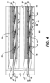
図1は、一例による、少なくとも1つの共通基板上に配置されたコンポーネントを含むコンピュータシステム100を示しており、少なくとも1つの共通基板は、ハウジングの内部にある。この例では、ハウジング102は、ハウジング内部の真空を維持するように構成され得る。こうして、コンピュータシステム100に対応するいくつかのコンポーネント(例えば、プロセッサ及びメモリ)は、真空を維持するハウジングの内部に配置される。ハウジング102は、いくつかの基板(例えば、基板104、106、及び108)を含み得る。これらの基板のそれぞれは、ガラス又は他の適切な材料、例えば様々なタイプのポリマーを用いて形成され得る。一例では、ガラス材料はホウケイ酸ガラスであってもよい。一例では、これらの基板のそれぞれは、一体物のガラス基板であってもよい。ハウジング102は、77K熱シールド112をさらに含み得、この熱シールド112は、77K熱シールド112の内部に配置された各基板の部分を熱的に分離するように構成され得る。77K熱シールド112は、図1に示されるパイプ120及び122のそれぞれを通って流れる液体ヘリウムを介して冷却され得る。液体ヘリウムを運ぶパイプ120及び122は、77K熱シールド112にろう付けされ得る。一例では、77K熱シールド112は、ニッケル鉄合金(例えば、Mu金属)を用いて形成され得る。77K熱シールド112はさらに、多層断熱材(図示せず)内に包まれてもよい。このようにして、77K熱シールド112は、4K空間と300K空間との間の熱的分離を効果的に提供し得る。一例では、超伝導コンポーネント(例えば、中央処理装置(CPU)、グラフィック処理装置(GPU)、人工知能プロセッサ、フィールドプログラマブルゲートアレイ(FPGA)、特定用途向け集積回路(ASIC)、特定用途向け標準製品(ASSP)、システムオンチップシステム(SOC)、コンプレックスプログラマブル論理装置(CPLD))は、各共通基板(104、106、108等)の第1の端部に向けて配置され得る。超伝導コンポーネントは、1次プロセッサ機能(主にプロセッサ機能)を提供するように構成され得る。本明細書で使用される「1次プロセッサ機能(primarily a processor functionality)」という語句は、処理機能を実行するために必要とされるあらゆる機能を含み得る。例として、限定ではなく、「1次プロセッサ機能(primary processor functionality)」という語句は、中央処理機能、グラフィック処理機能、人工知能機能、ゲートアレイ機能、メモリ機能、又はバス-インターフェイス管理機能のうちの少なくとも1つ(又は、それらの適切な組合せ)を含み得る。
FIG. 1 illustrates a
引き続き図1を参照すると、第1の端部は、超伝導デバイスが超伝導原理に一致して動作するのを可能にするのに適した温度に維持され得る。こうして、超伝導コンポーネントは、極低温(例えば、2Kから77K)に維持され得る。これは、熱分離と、液体ヘリウム又は他のそのような冷却液による冷却との組合せによって達成できる。一例として、銅の側壁130を、超伝導コンポーネントに隣接して取り付けてもよい。銅の側壁130はまた、図1に示されるように、パイプ(例えば、パイプ120)を通って流れる液体ヘリウムを介して冷却してもよい。一例では、極低温環境で動作するシステムは、適切に動作するために真空を必要とし得る。一例では、真空は、10-3トルから10-10トルの範囲の圧力に関連し得る。真空を使用することにより、伝達/対流がないことが確実になり、それにより、非常に異なる温度で動作するコンポーネントを同じ基板に取り付けることが可能になるので有利である。本明細書で言及する温度範囲は、これらのコンポーネントが動作している環境の温度に関係し、コンポーネント自体の温度に関係しないことを認識すべきである。こうして、コンポーネントが「動作している」又は「維持されている」等の言及は、これらのコンポーネントが、動作している、又は内部で維持されている環境の温度を指す。
With continued reference to FIG. 1, the first end may be maintained at a suitable temperature to enable the superconducting device to operate consistent with superconducting principles. Thus, superconducting components can be maintained at cryogenic temperatures (eg, 2K to 77K). This can be achieved by a combination of thermal isolation and cooling with liquid helium or other such cooling liquid. As an example, copper sidewalls 130 may be attached adjacent to the superconducting component. The
引き続き図1を参照すると、この例では、非超伝導コンポーネント(例えば、CMOS、BiCMOS、又は極低温を必要とせずに動作するのに適した他のタイプのデバイス)が、各共通基板(例えば、104、106、及び108)の第2の端部に向けて配置され得る。この例では、非超伝導コンポーネントは、不揮発性又は揮発性メモリコンポーネントのいずれかを含むメモリコンポーネントを含み得る。揮発性メモリコンポーネントは、ダイナミックランダムアクセスメモリ(DRAM)コンポーネントを含む、様々なタイプのランダムアクセスメモリコンポーネントのいずれかを含み得る。不揮発性メモリコンポーネントは、フラッシュメモリコンポーネントを含む、電力供給を受けていないときでも情報を格納できる様々なタイプのメモリコンポーネントのいずれかを含み得る。非超伝導コンポーネントは、フィールドプログラマブルゲートアレイ(FPGA)、特定用途向け集積回路(ASIC)、特定用途向け標準製品(ASSP)、システムオンチップシステム(SOC)、コンプレックスプログラマブル論理装置(CPLD)をさらに含み得る。こうして、非超伝導コンポーネントは1次ストレージ機能(主にストレージ機能)を提供し得るが、非超伝導コンポーネントは、ASIC、ASSP、SOC、CPLD等のコンポーネント、又は超伝導コンポーネントと非超伝導コンポーネントとの間の通信を調整して、DRAMを含むストレージデバイスの制御及び管理を処理できる他のタイプのコントローラを含み得る。本明細書で使用される「1次ストレージ機能(primarily a storage functionality)」という語句は、ストレージ機能を実行するために必要なあらゆる機能を含み得る。例として、限定ではなく、「1次ストレージ機能(primary storage functionality)」という語句は、メモリ機能、ゲートアレイ機能、バス管理機能、コントローラ機能、又はバス-インターフェイス管理機能のうちの少なくとも1つ(又は、それらの任意の適切な組合せ)を含み得る。 With continued reference to FIG. 1, in this example, non-superconducting components (e.g., CMOS, BiCMOS, or other types of devices suitable for operating without requiring cryogenic temperatures) are attached to each common substrate (e.g., 104, 106, and 108). In this example, non-superconducting components may include memory components, including either non-volatile or volatile memory components. Volatile memory components can include any of various types of random access memory components, including dynamic random access memory (DRAM) components. Non-volatile memory components may include any of various types of memory components capable of storing information even when unpowered, including flash memory components. Non-superconducting components further include Field Programmable Gate Arrays (FPGAs), Application Specific Integrated Circuits (ASICs), Application Specific Standard Products (ASSPs), System on Chip Systems (SOCs), Complex Programmable Logic Devices (CPLDs). obtain. Thus, the non-superconducting component may provide a primary storage function (mainly the storage function), but the non-superconducting component may be a component such as an ASIC, ASSP, SOC, CPLD, etc., or a superconducting component and a non-superconducting component. may include other types of controllers that can coordinate communications between and handle control and management of storage devices, including DRAMs. As used herein, the phrase "primarily a storage functionality" can include any functionality necessary to perform a storage function. By way of example, and not limitation, the phrase "primary storage functionality" may refer to at least one of memory functionality, gate array functionality, bus management functionality, controller functionality, or bus-interface management functionality (or , any suitable combination thereof).
引き続き図1を参照すると、非超伝導コンポーネントは、非極低温(例えば、200Kから400Kの間)に維持され得る。これは、熱分離と、水又は他の冷却液を用いた冷却との組合せによって達成できる。一例として、銅の側壁140を、非超伝導コンポーネントに隣接して取り付けてもよい。銅の側壁140はまた、図1に示されるように、パイプ(例えば、パイプ142及びパイプ144)を通って流れる水(又は、他の何らかの冷却液)を介して冷却してもよい。
With continued reference to FIG. 1, non-superconducting components can be maintained at non-cryogenic temperatures (eg, between 200K and 400K). This can be achieved by a combination of heat isolation and cooling with water or other cooling liquid. As an example, copper sidewalls 140 may be attached adjacent to non-superconducting components. The copper sidewalls 140 may also be cooled via water (or some other cooling fluid) flowing through pipes (eg,
引き続き図1を参照すると、超伝導コンポーネント及び非超伝導コンポーネントは、各共通基板(例えば、104、106、及び108)の上面又は下面に形成された回路トレースを用いて互いに通信することができる。回路トレースは、適切な製造プロセス(選択的レーザー焼結、溶融堆積モデリング、直接金属レーザー焼結、ステレオリソグラフィー、クラッディング、電子ビーム溶融、電子ビーム直接製造、エアロゾル噴射、インク噴射、半固体フリーフォーム製造、デジタル光処理、2光子重合、積層物体製造、3D印刷、又は他の同様の製造プロセスを含むが、これらに限定されない)を用いて形成され得る。一例では、回路トレースは、超伝導コンポーネントを含む基板の領域内のニオブ(又は、別の適切な超伝導材料)によって作製してもよい。この領域は、常伝導金属、例えば銅金属を除外し得る。他の領域では、回路トレースは、ニオブと、非超伝導コンポーネントを含む銅(或いは、超伝導金属と常伝導金属とを含む別の適切な金属又は金属合金)との両方によって作製してもよい。同じ基板上に配置された信号トレースを介して超伝導コンポーネント及び非超伝導コンポーネントが通信することにより、待ち時間(レイテンシ)を有利に低減することができる。これは、これらのコンポーネントが近接していると待ち時間が減少し得るためである。加えて、これは熱寄生を低減することもできる。図1が、コンポーネント、基板、及び他のコンポーネントの特定の配置を示しているが、これらは異なる方法で配置することができる。さらに、より少ないか又は追加のコンポーネント、基板、及び他のコンポーネントが存在し得る。 With continued reference to FIG. 1, superconducting and non-superconducting components can communicate with each other using circuit traces formed on the top or bottom surface of each common substrate (eg, 104, 106, and 108). Circuit traces are produced by appropriate fabrication processes (selective laser sintering, fused deposition modeling, direct metal laser sintering, stereolithography, cladding, e-beam melting, e-beam direct fabrication, aerosol jetting, ink jetting, semi-solid freeform manufacturing, digital light processing, two-photon polymerization, layered object manufacturing, 3D printing, or other similar manufacturing processes). In one example, circuit traces may be made of niobium (or another suitable superconducting material) in areas of the substrate that contain superconducting components. This region may exclude normal metals, such as copper metal. In other areas, circuit traces may be made of both niobium and copper with non-superconducting components (or another suitable metal or metal alloy including superconducting and normal metals). . Latency can be advantageously reduced by having superconducting and non-superconducting components communicate via signal traces located on the same substrate. This is because the proximity of these components can reduce latency. Additionally, it can also reduce thermal parasitics. Although FIG. 1 shows a particular arrangement of components, substrates, and other components, they can be arranged in different ways. Additionally, there may be fewer or additional components, substrates, and other components.
次に図2を参照すると、一例によるコンピュータシステム100の断面図200が示されている。図2に示される同じ又は同様のコンポーネントは、(図1と)同じ参照符号で参照される。この例では、超伝導コンポーネント230及び非超伝導コンポーネント240は、基板220に取り付けられるように示される。一例では、超伝導コンポーネントは、フリップチップボンディングを含む様々な技術のいずれかを用いて、各共通基板に取り付けられ得る。同様に、非超伝導コンポーネントは、フリップチップボンディングを含む様々な技術のいずれかを用いて、各共通基板に取り付けられ得る。これらのコンポーネントは、各共通基板に形成された信号ライン(後述する)を介して互いに通信することができる。熱シールド112は、超伝導コンポーネント230を非超伝導コンポーネント240から熱的に分離するために使用される。この例では、超伝導コンポーネント230は基板220の右端に向けて配置され、非超伝導コンポーネント240は共通基板220の左端に向けて配置される。このようにして、2つのタイプのコンポーネントは、熱シールド112によって熱的に分離される。熱シールド112及び他の熱分離特徴により、超伝導コンポーネントが極低温(例えば、9K未満)で動作し、非超伝導コンポーネントがかなり高い温度(例えば、10Kから400Kの間の範囲)動作することが可能になる。図2は、例えば銅の側壁250を含む、追加の熱分離コンポーネントを示す。また、図2は、後でさらに説明する銅ヒートシンク、例えば銅ヒートシンク260を示す。図2は、特定の方法で配置された特定の数のコンポーネントを示しているが、コンピュータシステム100は、異なるように配置されたより少ないか又は追加のコンポーネントを含み得る。
Referring now to FIG. 2, an example
一例によれば、図3は、断面図200に示されるコンピュータシステム100の一部の詳細図300を示す。詳細図300は、1次ストレージ機能(主にストレージ機能)を提供するように構成されるコンポーネントを含み得る非超伝導コンポーネント310を示す。さらに、前述したように、ヒートシンク320及びヒートシンク330は、非超伝導コンポーネントからの熱放射を低減するように構成され得る。これらのヒートシンクのそれぞれは、銅若しくは別の適切な熱伝導性金属又は合金を用いて作製することができる。ウェッジロック(wedge locks)316を使用して、ヒートシンクと、基板に取り付けられたコンポーネントを含む基板との間の緊密な結合を確実にすることができる。図3は、銅の側壁130にろう付けされ得るパイプ312をさらに示す。図3に示される特定の同様のコンポーネントは、図1及び図2と同じ参照符号を用いて番号付けされている。図3は、特定の方法で配置された特定の数のコンポーネントを示しているが、コンピュータシステム100は、異なるように配置されたより少ないか又は追加のコンポーネントを含み得る。
According to one example, FIG. 3 shows a
一例によれば、図4は、図1のコンピュータシステム100の一部の詳細図400を示す。詳細図400に示されるように、コンピュータシステム100は、前述したハウジングに配置された基板402及び404を含み得る。基板402は、平面に配置され、上面460及び下面462を有する。基板404は、異なる平面に配置され、また上面470及び下面472を有する。この例では、各基板の上面は、各基板の下面の反対側にある。この例では、超伝導コンポーネント406、408、及び410(又は、非超伝導コンポーネント)は、各基板402及び404の上面に取り付けられる。この例では、超伝導コンポーネントは、インジウムはんだ材料を用いて各基板に取り付けられ得る。銅のヒートシンク454、456、466、及び476が、超伝導コンポーネントから熱を除去するための熱経路を提供するように構成され得る。ばね力機構442、444、及び446等の機構を使用して、超伝導コンポーネント(例えば、406、408、及び410)を銅のヒートシンク466及び476とより近接した状態で接触させることができる。さらに、ウェッジロック(例えば、452)を使用して、基板(例えば、基板402)を銅の側壁にクランプして、基板及び共通基板に取り付けられたコンポーネントを冷却するための別の熱経路を提供することができる。この例では、基板402及び404に取り付けられたコンポーネントを熱伝導性材料(例えば、インジウムはんだ)でコーティング又は充填して、銅のヒートシンクと主にシリコンで作製されたコンポーネント(例えば、超伝導コンポーネントと非超伝導コンポーネントとの両方)との間の熱膨張係数(CTE)のミスマッチに対処することができる。図4は、特定の方法で配置された特定の数のコンポーネントを示しているが、コンピュータシステム100は、異なるように配置されたより少ないか又は追加のコンポーネントを含み得る。
According to one example, FIG. 4 shows a
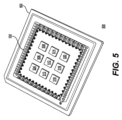
図5は、一例によるコンポーネント500(例えば、前述のコンポーネントのいずれか)を示す。コンポーネント500は、異なる位置に配置された、いくつかのダイを含み得る。ダイ504、506、508、510、512、514、516、518、及び520のそれぞれは、信号トレースを介して、コンポーネント500のベースにあるコネクタ(図示せず)に接続することができる。次に、これらのコネクタは、各コンポーネントを共通基板に取り付けるために、はんだボール又は他の取り付け機構に接続され得る。一例では、バンプパラメータは、位置毎に異なり得る。信号トレース又はラインは、コンポーネントの評価及びテストのために、チップバンプを周辺接続に接続し得る。図5は、特定の方法で配置された特定の数のダイを示しているが、コンポーネント500は、異なるように配置されたより少ないか又は追加のダイを含み得る。 FIG. 5 illustrates an example component 500 (eg, any of the components described above). Component 500 may include several dies arranged at different locations. Each of the dies 504, 506, 508, 510, 512, 514, 516, 518, and 520 can be connected to connectors (not shown) at the base of the component 500 via signal traces. These connectors can then be connected to solder balls or other attachment mechanisms to attach each component to a common substrate. In one example, bump parameters may vary from location to location. Signal traces or lines may connect chip bumps to peripheral connections for component evaluation and testing. Although FIG. 5 shows a particular number of dies arranged in a particular manner, component 500 may include fewer or additional dies arranged differently.
図6は、はんだバンプを用いて基板に結合されたコンポーネント(例えば、超伝導コンポーネント又は非超伝導コンポーネント)の断面図を示す。この例では、コンポーネント604は、インジウムバンプ612を用いて基板602に結合され得る。同様に、コンポーネント606は、インジウムバンプ614を用いて基板602に結合され得る。最後に、コンポーネント608は、インジウムバンプ616を用いて基板602に結合され得る。図6は、インジウムバンプを用いて基板に結合された特定の数のコンポーネントを示しているが、他の取り付け技術を使用してもよい。
FIG. 6 shows a cross-sectional view of a component (eg, superconducting or non-superconducting component) bonded to a substrate using solder bumps. In this example,
図7は、一例による超伝導コンポーネント700の断面図を示す。超伝導コンポーネント700は、基板上に形成された超伝導層及び誘電体層のスタックを含み得る。一例では、超伝導コンポーネントは、DCから10GHzを超える周波数を有する信号までの範囲の信号をサポートするように形成され得る。この例では、超伝導コンポーネントは、複数のダイに分離できる200mmウェーハ、300mmウェーハ、又はさらに大きなウェーハ等の大きなシリコン基板の上に製造できる。一例では、基板は、シリコン又は他の任意の断熱性又は伝導性材料から作製され得る。また、この例では、ニオブ又は同様の超伝導材料をスパッタリングすることにより、信号トレース及び接地面を形成することができる。一例として、窒化ニオブ(NbN)又は窒化ニオブチタン(NbTiN)等のニオブの化合物を使用してもよい。分子線エピタキシー(MBE)等の他の物理蒸着(PVD)法を使用してもよい。トレースに使用される材料のタイプに応じて、スパッタリングプロセス、化学蒸着(CVD)プロセス、プラズマ励起化学蒸着(PECVD)プロセス、蒸着プロセス、又は原子層堆積(ALD)プロセスを使用してもよい。こうして、例えば、NbN及びNbTiN等のニオブ化合物は、CVDプロセスを用いて形成することができる。
FIG. 7 shows a cross-sectional view of a
引き続き図7を参照すると、例示的な超伝導コンポーネント700では、誘電体層は、スピンオン・ポリイミド、ベンゾシクロブテン(BCB)、液晶ポリマー(LCP)、又は他の何らかのポリマー材料であり得る。超伝導コンポーネント700は、トレース又は接地面と同じ堆積ステップでニオブをコンフォーマル(conformal)に堆積させることによって形成することができるビアをさらに含み得る。ビアウェル(via wells)は、フォトイメージャブルポリイミドで直接パターン化するか、別のステップでエッチングできる。金属トレース及びビアは、同じ減法エッチングステップで規定できる。パッド接続は、インジウムはんだバンプ、錫-銀(Snag)はんだバンプ、金スタッドバンプ、銅ピラーバンプ、又は他の電気相互接続バンプタイプ等の、様々なワイヤボンド又はフリップチップバンプ及びワイヤボンド技術のTi/Au又はTi/Alパッドをサポートするように構成できる。
With continued reference to FIG. 7, in the
引き続き図7を参照すると、超伝導コンポーネントは、基板702の上に形成された誘電体層704を含み得る。基板702は、シリコン基板、サファイア基板、ガラス基板、又は任意の他の適切な基板であり得る。誘電体層704は、基板702上に誘電体(例えば、液晶ポリマー(LCP))を堆積させることによって形成され得る。超伝導層706が、誘電体層704の上に形成され得る。超伝導層706は、CVD又はPECVD等の堆積技術のいずれかを使用して、次にフォトリソグラフィを用いて堆積した材料をパターン化して形成され得る。この例では、超伝導層706は、誘電体層704の上にニオブを堆積させることによって形成され得る。フォトリソグラフィプロセスを使用して超伝導層706をパターン化し、超伝導ワイヤ又は他の超伝導構造を形成することができる。次に、化学機械研磨等のプロセスを用いて、超伝導層706の余分な部分を除去することができる。一例では、超伝導ワイヤは、ニオブ又は他の適切な金属を用いて形成してもよい。超伝導構造のレイアウトは、超伝導ワイヤ又は他の要素のレイアウトを形成するために使用される配置配線設計ツールを用いて形成され得る。一例として、フォトレジストは、超伝導ワイヤ又は金属層等の特定の層のレイアウトによって規定される他の構造として形成される、超伝導層706の領域のみを保護するようにパターン化され得る。他の超伝導金属又は金属合金をこのステップの一部として使用してもよい。一例では、ビア及びトレースは、トレースを形成するために使用されるものと同じ堆積ステップでのニオブのコンフォーマル堆積によって形成してもよい。ニオブは、スパッタリング又は他の同様のプロセスによって堆積させることができる。分子線エピタキシー(MBE)等の他の物理蒸着(PVD)法を使用してもよい。超伝導コンポーネント700は、超伝導層706の上に形成された誘電体層708をさらに含み得る。誘電体層708は、超伝導層706上に誘電体(例えば、液体ポリマー)を堆積させることによって形成され得る。一例では、誘電体層708は、超伝導層706上にポリイミドをスピンオンすることによって形成され得る。別の超伝導層が、誘電体層708の上に形成され得る。ビア710及び712は、誘電体層708にビア又はコンタクトホールを形成し、形成したそれらをニオブ又は類似の超伝導材料で充填することによって形成され得る。714、716、及び718を含む追加の超伝導トレースが、超伝導コンポーネントに含まれる次の超伝導層の一部として形成され得る。次に、誘電体層720が、超伝導トレース又は平面(例えば、超伝導トレース714、716、及び718を含む超伝導層)の上に形成されるように示される。誘電体層720は、超伝導層上に誘電体(例えば、液体ポリマー)を堆積させることによって形成され得る。一例では、誘電体層720は、超伝導層上にポリイミドをスピンオンすることによって形成され得る。次に、別の超伝導層が誘電体層720の上に形成され得る。ビアは、誘電体層720にビア又はコンタクトホールを形成し、形成したそれらをニオブ又は類似の超伝導材料で充填することによって形成され得る。724、726、及び728を含む追加の超伝導トレースが、超伝導コンポーネントに含まれる次の超伝導層の一部として形成され得る。一例では、超伝導ワイヤは、ニオブ又は他の適切な金属を用いて形成され得る。さらに別の誘電体層722は、超伝導トレース又は平面(例えば、超伝導トレース724、726、及び728を含む超伝導層)の上に形成されるように示される。誘電体層722は、超伝導層上に誘電体(例えば、液体ポリマー)を堆積させることによって形成され得る。一例では、誘電体層722は、超伝導層上にポリイミドをスピンオンすることによって形成され得る。次に、ビア730及び732並びに超伝導トレース734、736及び738が形成されるように示される。一例では、超伝導ワイヤは、ニオブ又は他の適切な金属を用いて形成され得る。次に、別の誘電体層740が形成され得る。この層は、前述したのと同様のプロセスを用いて形成され得る。次に、ビア742及び744並びに超伝導トレース750、752、754、756、及び758が形成されるように示される。一例では、超伝導ワイヤは、ニオブ又は他の適切な金属を用いて形成され得る。最後に、ビア764及び766は、パッド接続を提供するために形成されるように示される。パッド接続は、インジウムバンプ、C4バンプ、銅ピラー等の、様様なバンプ及びワイヤボンド技術のチタン/金(Ti/Au)又はチタン/アルミニウム(Ti/Al)パッドをサポートするように構成され得る。図7は、特定の方法で配置された超伝導コンポーネント700の特定の数の層を示しているが、異なるように配置されたより多い又はより少ない数の層があり得る。さらに、特定のステップは特定の順序で実行されるものとして説明しているが、超伝導コンポーネント700を製造するために、追加の又はより少ないステップを異なる順序で実行してもよい。
With continued reference to FIG. 7, a superconducting component may include a
引き続き図7を参照すると、一例では、超伝導層106は、超伝導コンポーネントを介してクロック信号を分配するように構成され得る。超伝導トレースの次のセット(例えば、超伝導トレース714、716、及び718)は、超伝導コンポーネントを介してクロック信号を分配するように構成され得る。超伝導トレースの次のセット(例えば、超伝導トレース724、726、及び728)が、超伝導コンポーネントの接地面として機能するように構成され得る。超伝導トレースの次のセット(例えば、超伝導トレース734、736、及び738)が、超伝導コンポーネントを介してクロック信号以外の信号を分配するように構成され得る。超伝導トレースの次のセット(例えば、超伝導トレース750、752、754、756、及び758)が、超伝導コンポーネントを介してクロック信号以外の信号を分配するように構成され得る。実際に、様々な超伝導層の機能は、超伝導コンポーネントに関連する要件に基づいて変更できる。
With continued reference to FIG. 7, in one example,
図8は、一例による、基板800の長さに沿った温度の変化を示すグラフ820を含む基板800を示す。基板800は、基板層802、非超伝導コンポーネント層804、超伝導コンポーネント層806、及びヒートシンク808を含む。この例では、厚い(従って、高熱伝導性)銅ヒートシンク808を使用して、基板800の実質的な長さに沿って低温のメンテナンスを実現する。コンポーネント層は、様々なメカニズムを介して基板層802に取り付けられたチップを含み得る。銅のヒートシンク808は、超伝導コンポーネントを超伝導コンポーネント層806の一部として形成することができ、ヒートシンク808がそれらを覆わないように構成される。グラフ820は、基板800が配置される環境の温度の変化を示す。こうして、プロセッサ側の温度は約4Kであり、メモリ側の温度は約300Kである。基板800の長さに沿った温度のこの変化にもかかわらず、前述した様々な技術及び方法論は、超伝導コンポーネントと非超伝導コンポーネントとの両方の適切な動作を保証する。
FIG. 8 shows a
結論として、本開示の一態様では、ハウジングを含むコンピュータシステムが提供され、ハウジングの外部の大気圧よりも低い圧力がハウジングの内部に維持される。一例では、より低い圧力は、10-3トルから10-10トルの間の範囲にあり得る。 In conclusion, in one aspect of the present disclosure, a computer system is provided that includes a housing to maintain a pressure inside the housing that is less than atmospheric pressure outside the housing. In one example, the lower pressure can range between 10 −3 Torr and 10 −10 Torr.
コンピュータシステムは、ハウジングの内部にあり、且つ第1の面と、第1の面に平行な第2の面とを有する第1の平面に配置された第1の基板をさらに含み得、第2の面は第1の面の反対側にあり、第1の複数のコンポーネントの第1のセットが、第1の基板の第1の端部に向けて第2の面に取り付けられ、第2の複数のコンポーネントの第2のセットが、第1の基板の第2の端部に向けて第2の面に取り付けられ、第1の端部は第2の端部の反対側にあり、第1の複数のコンポーネントのそれぞれが、1次プロセッサ機能(主にプロセッサ機能)を提供するように構成され、第2の複数のコンポーネントのそれぞれが、1次ストレージ機能(主にストレージ機能)を提供するように構成される。 The computer system may further include a first substrate within the housing and arranged in a first plane having a first side and a second side parallel to the first side; is opposite the first side, a first set of the first plurality of components is mounted on the second side toward the first end of the first substrate, and the second A second set of components is mounted on the second side of the first substrate toward the second end, the first end opposite the second end, the first each of the plurality of components is configured to provide primary processor functionality (primarily processor functionality) and each of the second plurality of components is configured to provide primary storage functionality (primarily storage functionality) configured to
コンピュータシステムは、ハウジングの内部にあり、且つ第1の平面より上又は下の第2の平面に配置された第2の基板をさらに含み得、第2の基板は、第2の平面に平行な第3の面及び第4の面を有しており、第4の面は第3の面の反対側にあり、第1の複数のコンポーネントの第3のセットが、第2の基板の第3の端部に向けて第4の面に取り付けられ、第2の複数のコンポーネントの第4のセットが、第2の基板の第4の端部に向けて第4の面に取り付けられ、第3の端部は第4の端部の反対側にあり、第1の基板及び第2の基板のそれぞれが、第1の複数のコンポーネントの少なくともサブセットを第2の複数のコンポーネントの少なくともサブセットと相互接続するための複数の回路トレースを含む。複数の回路トレースのそれぞれは、超伝導金属を含むが常伝導金属を除く第1の領域と、超伝導金属と常伝導金属との両方を含む第2の領域とを含み得る。 The computer system may further include a second substrate within the housing and positioned in a second plane above or below the first plane, the second substrate parallel to the second plane. It has a third side and a fourth side, the fourth side opposite the third side, and a third set of the first plurality of components on the second substrate. a fourth set of a second plurality of components mounted on the fourth side toward the fourth end of the second substrate; a third is opposite the fourth end, and the first substrate and the second substrate each interconnect at least a subset of the first plurality of components with at least a subset of the second plurality of components. Includes multiple circuit traces for Each of the plurality of circuit traces may include a first region containing superconducting metal but excluding normal metal and a second region containing both superconducting metal and normal metal.
コンピュータシステムは、第1の複数のコンポーネントのそれぞれが第1の温度で動作するように構成され、且つ第2の複数のコンポーネントのそれぞれが第1の温度より高い第2の温度で動作するように構成されるように、第1の基板の第1の端部を第2の端部から熱的に分離し、且つ第2の基板の第3の端部を第4の端部から熱的に分離するように構成された熱シールドをさらに含み得、第1の温度は2ケルビンから77ケルビンの間の範囲にあり、第2の温度は200ケルビンから400ケルビンの間の範囲にある。 The computer system is configured so that each of the first plurality of components operates at a first temperature and each of the second plurality of components operates at a second temperature that is higher than the first temperature. so that the first end of the first substrate is thermally isolated from the second end and the third end of the second substrate is thermally isolated from the fourth end. A heat shield configured to provide isolation may further include a first temperature ranging between 2 Kelvin and 77 Kelvin and a second temperature ranging between 200 Kelvin and 400 Kelvin.
1次プロセッサ機能は、中央処理機能、グラフィック処理機能、人工知能機能、ゲートアレイ機能、メモリ機能、又はバス-インターフェイス管理機能のうちの少なくとも1つを含み得る。1次ストレージ機能は、メモリ機能、ゲートアレイ機能、バス管理機能、コントローラ機能、又はバス-インターフェイス管理機能のうちの少なくとも1つを含み得る。 The primary processor functions may include at least one of central processing functions, graphics processing functions, artificial intelligence functions, gate array functions, memory functions, or bus-interface management functions. The primary storage functions may include at least one of memory functions, gate array functions, bus management functions, controller functions, or bus-interface management functions.
第1の複数のコンポーネントのそれぞれは、中央処理装置、グラフィック処理装置、人工知能プロセッサ、フィールドプログラマブルゲートアレイ、特定用途向け集積回路、特定用途向け標準製品、システムオンチップ、コンプレックスプログラマブル論理装置、ランダムアクセスメモリ、及びジョセフソン磁気ランダムアクセスメモリを含むグループから選択され得る。第2の複数のコンポーネントのそれぞれは、ダイナミックランダムアクセスメモリ、フィールドプログラマブルゲートアレイ、特定用途向け集積回路、特定用途向け標準製品、システムオンチップ、及びコンプレックスプログラマブル論理装置を含むグループから選択され得る。 Each of the first plurality of components includes: a central processing unit, a graphics processing unit, an artificial intelligence processor, a field programmable gate array, an application specific integrated circuit, an application specific standard product, a system on chip, a complex programmable logic device, a random access memory, and Josephson magnetic random access memory. Each of the second plurality of components may be selected from a group including dynamic random access memory, field programmable gate array, application specific integrated circuit, application specific standard product, system on chip, and complex programmable logic device.
本開示の別の態様では、ハウジングを含むコンピュータシステムが提供され、ハウジングの内部で真空が維持される。一例では、真空は、10-3トルから10-10トルの間の範囲の圧力に対応し得る。 In another aspect of the disclosure, a computer system is provided that includes a housing, and a vacuum is maintained within the housing. In one example, the vacuum may correspond to pressures ranging between 10 −3 Torr and 10 −10 Torr.
コンピュータシステムは、ハウジングの内部にあり、且つ第1の面と、第1の面に平行な第2の面とを有する第1の平面に配置された第1の基板をさらに含み得、第2の面は第1の面の反対側にあり、第1の複数のコンポーネントの第1のセットが、第1の基板の第1の端部に向けて第2の面に取り付けられ、第2の複数のコンポーネントの第2のセットが、第1の基板の第2の端部に向けて第2の面に取り付けられ、第1の端部は第2の端部の反対側にあり、第1の複数のコンポーネントのそれぞれが、1次プロセッサ機能(主にプロセッサ機能)を提供するように構成され、第2の複数のコンポーネントのそれぞれが、1次ストレージ機能(主にストレージ機能)を提供するように構成される。 The computer system may further include a first substrate within the housing and arranged in a first plane having a first side and a second side parallel to the first side; is opposite the first side, a first set of the first plurality of components is mounted on the second side toward the first end of the first substrate, and the second A second set of components is mounted on the second side of the first substrate toward the second end, the first end opposite the second end, the first each of the plurality of components is configured to provide primary processor functionality (primarily processor functionality) and each of the second plurality of components is configured to provide primary storage functionality (primarily storage functionality) configured to
コンピュータシステムは、ハウジングの内部にあり、且つ第1の平面より上又は下の第2の平面に配置された第2の基板をさらに含み得、第2の基板は、第2の平面に平行な第3の面及び第4の面を有しており、第4の面は第3の面の反対側にあり、第1の複数のコンポーネントの第3のセットが、第2の基板の第3の端部に向けて第4の面に取り付けられ、第2の複数のコンポーネントの第4のセットが、第2の基板の第4の端部に向けて第4の面に取り付けられ、第3の端部は第4の端部の反対側にあり、第1の基板及び第2の基板のそれぞれが、第1の複数のコンポーネントの少なくともサブセットを第2の複数のコンポーネントの少なくともサブセットと相互接続するための複数の回路トレースを含む。複数の回路トレースのそれぞれが、超伝導金属を含むが常伝導金属を除く第1の領域と、超伝導金属と常伝導金属との両方を含む第2の領域とを含み得る。 The computer system may further include a second substrate within the housing and positioned in a second plane above or below the first plane, the second substrate parallel to the second plane. It has a third side and a fourth side, the fourth side opposite the third side, and a third set of the first plurality of components on the second substrate. a fourth set of a second plurality of components mounted on the fourth side toward the fourth end of the second substrate; a third is opposite the fourth end, and the first substrate and the second substrate each interconnect at least a subset of the first plurality of components with at least a subset of the second plurality of components. Includes multiple circuit traces for Each of the plurality of circuit traces may include a first region containing superconducting metal but excluding normal metal and a second region containing both superconducting metal and normal metal.
コンピュータシステムは、第1の複数のコンポーネントのそれぞれが第1の温度で動作するように構成され、且つ第2の複数のコンポーネントのそれぞれが第1の温度より高い第2の温度で動作するように構成されるように、第1の基板の第1の端部を第2の端部から熱的に分離し、且つ第2の基板の第3の端部を第4の端部から熱的に分離するように構成された熱シールドをさらに含み得、第1の温度は2ケルビンから77ケルビンの間の範囲にあり、第2の温度は200ケルビンから400ケルビンの間の範囲にある。 The computer system is configured so that each of the first plurality of components operates at a first temperature and each of the second plurality of components operates at a second temperature that is higher than the first temperature. so that the first end of the first substrate is thermally isolated from the second end and the third end of the second substrate is thermally isolated from the fourth end. A heat shield configured to provide isolation may further include a first temperature ranging between 2 Kelvin and 77 Kelvin and a second temperature ranging between 200 Kelvin and 400 Kelvin.
1次プロセッサ機能は、中央処理機能、グラフィック処理機能、人工知能機能、ゲートアレイ機能、メモリ機能、又はバス-インターフェイス管理機能のうちの少なくとも1つを含み得る。1次ストレージ機能は、メモリ機能、ゲートアレイ機能、バス管理機能、コントローラ機能、又はバス-インターフェイス管理機能のうちの少なくとも1つを含み得る。 The primary processor functions may include at least one of central processing functions, graphics processing functions, artificial intelligence functions, gate array functions, memory functions, or bus-interface management functions. The primary storage functions may include at least one of memory functions, gate array functions, bus management functions, controller functions, or bus-interface management functions.
第1の複数のコンポーネントのそれぞれは、中央処理装置、グラフィック処理装置、人工知能プロセッサ、フィールドプログラマブルゲートアレイ、特定用途向け集積回路、特定用途向け標準製品、システムオンチップ、コンプレックスプログラマブル論理装置、ランダムアクセスメモリ、ジョセフソン磁気ランダムアクセスメモリを含むグループから選択され得る。第2の複数のコンポーネントのそれぞれは、ダイナミックランダムアクセスメモリ、フィールドプログラマブルゲートアレイ、特定用途向け集積回路、特定用途向け標準製品、システムオンチップ、及びコンプレックスプログラマブル論理装置を含むグループから選択され得る。 Each of the first plurality of components includes: a central processing unit, a graphics processing unit, an artificial intelligence processor, a field programmable gate array, an application specific integrated circuit, an application specific standard product, a system on chip, a complex programmable logic device, a random access memory, may be selected from the group including Josephson Magnetic Random Access Memory. Each of the second plurality of components may be selected from a group including dynamic random access memory, field programmable gate array, application specific integrated circuit, application specific standard product, system on chip, and complex programmable logic device.
さらに別の態様では、本開示は、ハウジングを含むコンピュータシステムに関し、ハウジングの内部で真空が維持される。一例では、真空は、10-3トルから10-10トルの間の範囲の圧力に対応し得る。 In yet another aspect, the present disclosure relates to a computer system including a housing in which a vacuum is maintained within the housing. In one example, the vacuum may correspond to pressures ranging between 10 −3 Torr and 10 −10 Torr.
コンピュータシステムは、ハウジングの内部にあり、且つ第1の面と、第1の面に平行な第2の面とを有する第1の平面に配置された第1の基板をさらに含み得、第2の面は第1の面の反対側にあり、第1の複数のコンポーネントの第1のセットが、第1の基板の第1の端部に向けて第2の面に取り付けられ、第2の複数のコンポーネントの第2のセットが、第1の基板の第2の端部に向けて第2の面に取り付けられ、第1の端部は第2の端部の反対側にあり、第1の複数のコンポーネントのそれぞれが、1次プロセッサ機能(主にプロセッサ機能)を提供するように構成され、第2の複数のコンポーネントのそれぞれが、1次ストレージ機能(主にストレージ機能)を提供するように構成され、第1のヒートシンクが、第1の基板に熱的にクランプするように第1の基板に結合される。 The computer system may further include a first substrate within the housing and arranged in a first plane having a first side and a second side parallel to the first side; is opposite the first side, a first set of the first plurality of components is mounted on the second side toward the first end of the first substrate, and the second A second set of components is mounted on the second side of the first substrate toward the second end, the first end opposite the second end, the first each of the plurality of components is configured to provide primary processor functionality (primarily processor functionality) and each of the second plurality of components is configured to provide primary storage functionality (primarily storage functionality) wherein a first heat sink is coupled to the first substrate to thermally clamp to the first substrate.
コンピュータシステムは、ハウジングの内部にあり、且つ第1の平面より上又は下の第2の平面に配置された第2の基板をさらに含み得、第2の基板は、第2の平面に平行な第3の面及び第4の面を有しており、第4の面は第3の面の反対側にあり、第1の複数のコンポーネントの第3のセットが、第2の基板の第3の端部に向けて第4の面に取り付けられ、第2の複数のコンポーネントの第4のセットが、第2の基板の第4の端部に向けて第4の面に取り付けられ、第3の端部は第4の端部の反対側にあり、第1の基板及び第2の基板のそれぞれが、第1の複数のコンポーネントの少なくともサブセットを第2の複数のコンポーネントの少なくともサブセットと相互接続するための複数の回路トレースを含み、第2のヒートシンクが、第2の基板を熱的にクランプするように第2の基板に結合される。 The computer system may further include a second substrate within the housing and positioned in a second plane above or below the first plane, the second substrate parallel to the second plane. It has a third side and a fourth side, the fourth side opposite the third side, and a third set of the first plurality of components on the second substrate. a fourth set of a second plurality of components mounted on the fourth side toward the fourth end of the second substrate; a third is opposite the fourth end, and the first substrate and the second substrate each interconnect at least a subset of the first plurality of components with at least a subset of the second plurality of components. A second heat sink is coupled to the second substrate to thermally clamp the second substrate.
コンピュータシステムは、第1の複数のコンポーネントのそれぞれが第1の温度で動作するように構成され、且つ第2の複数のコンポーネントのそれぞれが第1の温度より高い第2の温度で動作するように構成されるように、第1の基板の第1の端部を第2の端部から熱的に分離し、且つ第2の基板の第3の端部を第4の端部から熱的に分離するように構成された熱シールドをさらに含み得、第1の温度は9ケルビン未満であり、第2の温度は80ケルビンから400ケルビンの間の範囲にある。 The computer system is configured so that each of the first plurality of components operates at a first temperature and each of the second plurality of components operates at a second temperature that is higher than the first temperature. so that the first end of the first substrate is thermally isolated from the second end and the third end of the second substrate is thermally isolated from the fourth end. A heat shield configured to provide isolation may further include a first temperature less than 9 Kelvin and a second temperature in a range between 80 Kelvin and 400 Kelvin.
1次プロセッサ機能は、中央処理機能、グラフィック処理機能、人工知能機能、ゲートアレイ機能、メモリ機能、又はバス-インターフェイス管理機能のうちの少なくとも1つを含み得る。1次ストレージ機能は、メモリ機能、ゲートアレイ機能、バス管理機能、コントローラ機能、又はバス-インターフェイス管理機能のうちの少なくとも1つを含み得る。 The primary processor functions may include at least one of central processing functions, graphics processing functions, artificial intelligence functions, gate array functions, memory functions, or bus-interface management functions. The primary storage functions may include at least one of memory functions, gate array functions, bus management functions, controller functions, or bus-interface management functions.
第1の複数のコンポーネントのそれぞれは、中央処理装置、グラフィック処理装置、人工知能プロセッサ、フィールドプログラマブルゲートアレイ、特定用途向け集積回路、特定用途向け標準製品、システムオンチップ、コンプレックスプログラマブル論理装置、ランダムアクセスメモリ、及びジョセフソン磁気ランダムアクセスメモリを含むグループから選択され得る。第2の複数のコンポーネントのそれぞれは、ダイナミックランダムアクセスメモリ、フィールドプログラマブルゲートアレイ、特定用途向け集積回路、特定用途向け標準製品、システムオンチップ、及びコンプレックスプログラマブル論理装置を含むグループから選択され得る。 Each of the first plurality of components includes: a central processing unit, a graphics processing unit, an artificial intelligence processor, a field programmable gate array, an application specific integrated circuit, an application specific standard product, a system on chip, a complex programmable logic device, a random access memory, and Josephson magnetic random access memory. Each of the second plurality of components may be selected from a group including dynamic random access memory, field programmable gate array, application specific integrated circuit, application specific standard product, system on chip, and complex programmable logic device.
本明細書に示される方法、モジュール、及びコンポーネントは単なる例示であることを理解されたい。例えば、限定はしないが、超伝導デバイスの例示的なタイプには、フィールドプログラマブルゲートアレイ(FPGA)、特定用途向け集積回路(ASIC)、特定用途向け標準製品(ASSP)、システムオンチップシステム(SOC)、コンプレックスプログラマブル論理装置(CPLD)等が含まれ得る。 It should be understood that the methods, modules, and components presented herein are merely examples. For example, without limitation, exemplary types of superconducting devices include field programmable gate arrays (FPGAs), application specific integrated circuits (ASICs), application specific standard products (ASSPs), system-on-chip systems (SOCs). ), Complex Programmable Logic Devices (CPLDs), and the like.
さらに、抽象的であるが依然として明確な意味で、同じ機能を達成するためのコンポーネントの配置は、所望の機能が達成されるように効果的に「関連付け」られる。従って、特定の機能を達成するために本明細書で組み合わされる任意の2つのコンポーネントは、アーキテクチャ又は中間コンポーネントに関係なく、所望の機能が達成されるように互いに「関連付けられる」と見なすことができる。同様に、そのように関連付けられた2つのコンポーネントも、所望の機能を達成するように、互いに「動作可能に接続」又は「結合」されていると見なすこともできる。 Moreover, in an abstract but still definite sense, the arrangement of components to accomplish the same functionality are effectively "related" such that the desired functionality is achieved. Thus, any two components that are combined herein to achieve a particular function can be considered "associated" with each other such that the desired function is achieved, regardless of the architecture or intermediate components. . Similarly, two components that are so associated may also be considered "operably connected" or "coupled" together to achieve a desired function.
さらに、当業者は、上述の動作の機能の間の境界が単なる例示であることを認識するであろう。複数の動作の機能を単一の動作に組み合わせることができ、及び/又は単一の動作の機能を追加の動作に分配させることができる。さらに、代替の実施形態は、特定の動作の複数のインスタンスを含み得、動作の順序は、他の様々な実施形態において変更され得る。 Furthermore, those skilled in the art will recognize that the boundaries between the functions of the operations described above are merely exemplary. Functionality of multiple operations can be combined into a single operation and/or functionality of a single operation can be distributed among additional operations. Additionally, alternate embodiments may include multiple instances of a particular operation, and the order of the operations may be altered in various other embodiments.
本開示は特定の例を提供するが、以下の特許請求の範囲に記載される本開示の範囲から逸脱することなく、様々な修正及び変更を行うことができる。従って、明細書及び図面は、限定的な意味ではなく例示的な意味で見なされるべきであり、そのような修正は全て、本開示の範囲内に含まれることが意図される。特定の例に関して本明細書に記載される利益、利点、又は問題の解決策は、いずれか又は全ての請求項の重要な、必須の、又は本質的な特徴又は要素として解釈されることを意図していない。 Although this disclosure provides specific examples, various modifications and changes can be made without departing from the scope of this disclosure as set forth in the following claims. Accordingly, the specification and drawings are to be regarded in an illustrative rather than a restrictive sense, and all such modifications are intended to be included within the scope of the present disclosure. Any benefit, advantage, or solution to a problem described herein with respect to a particular example is intended to be construed as an important, essential, or essential feature or element of any or all claims. not.
さらに、本明細書で使用される「1つの(a, an)」という用語は、1つ又は2つ以上として規定される。また、請求項における「少なくとも1つ」及び「1つ又は複数」等の導入句の使用は、不定冠詞「1つの、ある(a, an)」による別のクレーム要素の導入が、同じクレームに導入句「1つ又は複数」又は「少なくとも1つ」と「1つの(a, an)」等の不定冠詞が含まれている場合でも、そのように導入されたクレーム要素を含む特定のクレームをそのような要素を1つだけ含む発明に制限を意味するものと解釈してはならない。明確な製品の使用についても同じことが当てはまる。 Additionally, the term "a, an" as used herein is defined as one or more than one. Also, the use of introductory phrases such as "at least one" and "one or more" in a claim indicates that the introduction of another claim element by the indefinite article "a, an" does not apply to the same claim. Indefinite articles such as the introductory phrase "one or more" or "at least one" and "a, an" do not preclude a particular claim that includes claim elements so introduced. They should not be construed as being limited to the invention containing only one such element. The same applies to the use of distinct products.
特に明記しない限り、「第1」及び「第2」等の用語は、そのような用語が説明する要素を適宜区別するために使用される。こうして、これらの用語は、必ずしもそのような要素の時間的又は他の優先順位付けを示すことを意図するものではない。
Unless otherwise stated, terms such as "first" and "second" are used to arbitrarily distinguish between the elements such terms describe. Thus, these terms are not necessarily intended to imply a temporal or other prioritization of such elements.
Claims (13)
ハウジングであって、該ハウジングの外部の大気圧よりも低い圧力が前記ハウジングの内部に維持される、ハウジングと、
第1の複数のコンポーネントと、
第2の複数のコンポーネントと、
第1の面と、該第1の面に平行な第2の面とを有する第1の平面に配置された第1の基板であって、前記第2の面は前記第1の面の反対側にあり、前記第1の複数のコンポーネントの第1のセットが、前記第1の基板の前記ハウジング内にある第1の端部に向けて前記第2の面に取り付けられ、前記第2の複数のコンポーネントの第2のセットが、前記第1の基板の前記ハウジング外にある第2の端部に向けて前記第2の面に取り付けられ、前記第1の端部は前記第2の端部の反対側にあり、前記第1の複数のコンポーネントのそれぞれが、1次プロセッサ機能を提供するように構成され、前記第2の複数のコンポーネントのそれぞれが、1次ストレージ機能を提供するように構成される、第1の基板と、
前記第1の平面より上又は下の第2の平面に配置された第2の基板であって、該第2の基板は、前記第2の平面に平行な第3の面及び第4の面を有しており、該第4の面は前記第3の面の反対側にあり、前記第1の複数のコンポーネントの第3のセットが、前記第2の基板の前記ハウジング内にある第3の端部に向けて前記第4の面に取り付けられ、前記第2の複数のコンポーネントの第4のセットが、前記第2の基板の前記ハウジング外にある第4の端部に向けて前記第4の面に取り付けられ、前記第3の端部は前記第4の端部の反対側にあり、前記第1の基板及び前記第2の基板のそれぞれが、前記第1の複数のコンポーネントの少なくともサブセットを前記第2の複数のコンポーネントの少なくともサブセットと相互接続するための複数の回路トレースを含む、第2の基板と、
前記第1の複数のコンポーネントのそれぞれが第1の温度で動作するように構成され、且つ前記第2の複数のコンポーネントのそれぞれが前記第1の温度より高い第2の温度で動作するように構成されるように、前記第1の基板の前記第1の端部を前記第2の端部から熱的に分離し、且つ前記第2の基板の前記第3の端部を前記第4の端部から熱的に分離するように構成された熱シールドであって、前記第1の温度は2ケルビンから77ケルビンの間の範囲にあり、前記第2の温度は200ケルビン(K)から400ケルビンの間の範囲にある、熱シールドと、を含む、
コンピュータシステム。 A computer system, the computer system comprising:
a housing, wherein a pressure is maintained inside the housing that is less than the atmospheric pressure outside the housing;
a first plurality of components;
a second plurality of components;
A first substrate arranged in a first plane having a first side and a second side parallel to the first side, the second side being opposite the first side a first set of the first plurality of components mounted on the second surface toward a first end within the housing of the first substrate; A second set of components is mounted on the second surface toward a second end outside the housing of the first substrate, the first end connecting to the second end. on opposite sides of the unit, each of the first plurality of components configured to provide primary processor functionality and each of the second plurality of components to provide primary storage functionality. a first substrate, comprising:
a second substrate disposed in a second plane above or below the first plane, the second substrate having a third plane parallel to the second plane and a fourth plane; a surface, the fourth surface opposite the third surface, and a third set of the first plurality of components located within the housing of the second substrate; A fourth set of the second plurality of components mounted on the fourth surface toward an end of 3, and a fourth set of the second plurality of components mounted toward a fourth end outside the housing of the second substrate. Mounted on a fourth surface, the third end opposite the fourth end, and each of the first substrate and the second substrate of the first plurality of components. a second substrate comprising a plurality of circuit traces for interconnecting at least a subset with at least a subset of said second plurality of components;
each of the first plurality of components configured to operate at a first temperature and each of the second plurality of components configured to operate at a second temperature greater than the first temperature thermally isolating the first end of the first substrate from the second end and connecting the third end of the second substrate to the fourth end such that a heat shield configured to thermally isolate from a part, wherein the first temperature is in the range between 2 Kelvin and 77 Kelvin and the second temperature is between 200 Kelvin (K) and 400 Kelvin; a heat shield ranging between
computer system.
ハウジングであって、該ハウジングの内部で真空が維持されるハウジングと、
第1の複数のコンポーネントと、
第2の複数のコンポーネントと、
第1の面と、該第1の面に平行な第2の面とを有する第1の平面に配置された第1の基板であって、前記第2の面は前記第1の面の反対側にあり、前記第1の複数のコンポーネントの第1のセットが、前記第1の基板の前記ハウジング内にある第1の端部に向けて前記第2の面に取り付けられ、前記第2の複数のコンポーネントの第2のセットが、前記第1の基板の前記ハウジング外にある第2の端部に向けて前記第2の面に取り付けられ、前記第1の端部は前記第2の端部の反対側にあり、前記第1の複数のコンポーネントのそれぞれが、1次プロセッサ機能を提供するように構成され、前記第2の複数のコンポーネントのそれぞれが、1次ストレージ機能を提供するように構成され、第1のヒートシンクが、前記第1の基板を熱的にクランプするように前記第1の基板に結合される、第1の基板と、
前記ハウジングの内部にあり、且つ前記第1の平面より上又は下の第2の平面に配置された第2の基板であって、該第2の基板は、前記第2の平面に平行な第3の面及び第4の面を有しており、該第4の面は前記第3の面の反対側にあり、前記第1の複数のコンポーネントの第3のセットが、前記第2の基板の前記ハウジング内にある第3の端部に向けて前記第4の面に取り付けられ、前記第2の複数のコンポーネントの第4のセットが、前記第2の基板の前記ハウジング外にある第4の端部に向けて前記第4の面に取り付けられ、前記第3の端部は前記第4の端部の反対側にあり、前記第1の基板及び前記第2の基板のそれぞれが、前記第1の複数のコンポーネントの少なくともサブセットを前記第2の複数のコンポーネントの少なくともサブセットと相互接続するための複数の回路トレースを含み、第2のヒートシンクが、前記第2の基板を熱的にクランプするように前記第2の基板に結合される、第2の基板と、
前記第1の複数のコンポーネントのそれぞれが第1の温度で動作するように構成され、且つ前記第2の複数のコンポーネントのそれぞれが前記第1の温度より高い第2の温度で動作するように構成されるように、前記第1の基板の前記第1の端部を前記第2の端部から熱的に分離し、且つ前記第2の基板の前記第3の端部を前記第4の端部から熱的に分離するように構成された熱シールドであって、前記第1の温度は9ケルビン未満であり、前記第2の温度は80ケルビンから400ケルビンの範囲にある、熱シールドと、を含む、
コンピュータシステム。 A computer system, the computer system comprising:
a housing in which a vacuum is maintained within the housing;
a first plurality of components;
a second plurality of components;
A first substrate arranged in a first plane having a first side and a second side parallel to the first side, the second side being opposite the first side a first set of the first plurality of components mounted on the second surface toward a first end within the housing of the first substrate; A second set of components is mounted on the second surface toward a second end outside the housing of the first substrate, the first end connecting to the second end. on opposite sides of the unit, each of the first plurality of components configured to provide primary processor functionality and each of the second plurality of components to provide primary storage functionality. a first substrate configured, wherein a first heat sink is coupled to said first substrate to thermally clamp said first substrate;
A second substrate within the housing and positioned in a second plane above or below the first plane, the second substrate being parallel to the second plane. a third side and a fourth side, the fourth side opposite the third side, the third set of the first plurality of components being mounted on the second substrate; a fourth set of the second plurality of components mounted on the fourth surface toward a third end within the housing of the second substrate and a fourth set of components outside the housing of the second substrate; wherein the third end is opposite the fourth end, and each of the first substrate and the second substrate is attached to the fourth surface toward the end of the a plurality of circuit traces for interconnecting at least a subset of the first plurality of components with at least a subset of the second plurality of components, and a second heat sink thermally clamping the second substrate. a second substrate coupled to the second substrate such that
each of the first plurality of components configured to operate at a first temperature and each of the second plurality of components configured to operate at a second temperature greater than the first temperature thermally isolating the first end of the first substrate from the second end and connecting the third end of the second substrate to the fourth end such that a heat shield configured to thermally isolate from a portion, wherein the first temperature is less than 9 Kelvin and the second temperature is in the range of 80 Kelvin to 400 Kelvin; including,
computer system.
Applications Claiming Priority (3)
| Application Number | Priority Date | Filing Date | Title |
|---|---|---|---|
| US15/921,311 | 2018-03-14 | ||
| US15/921,311 US10165667B1 (en) | 2018-03-14 | 2018-03-14 | Computing system with superconducting and non-superconducting components located on a common substrate |
| PCT/US2018/063509 WO2019177673A1 (en) | 2018-03-14 | 2018-12-01 | Computing system with superconducting and non-superconducting components located on a common substrate |
Publications (3)
| Publication Number | Publication Date |
|---|---|
| JP2021517294A JP2021517294A (en) | 2021-07-15 |
| JP2021517294A5 JP2021517294A5 (en) | 2021-12-09 |
| JP7304872B2 true JP7304872B2 (en) | 2023-07-07 |
Family
ID=64692269
Family Applications (1)
| Application Number | Title | Priority Date | Filing Date |
|---|---|---|---|
| JP2020546095A Active JP7304872B2 (en) | 2018-03-14 | 2018-12-01 | Computer system with superconducting and non-superconducting components on a common substrate |
Country Status (13)
| Country | Link |
|---|---|
| US (1) | US10165667B1 (en) |
| EP (1) | EP3765939A1 (en) |
| JP (1) | JP7304872B2 (en) |
| KR (1) | KR102609929B1 (en) |
| CN (1) | CN111837093B (en) |
| AU (1) | AU2018413356B2 (en) |
| BR (1) | BR112020016789A2 (en) |
| CA (1) | CA3092180A1 (en) |
| IL (1) | IL277082B1 (en) |
| MX (1) | MX2020009402A (en) |
| PH (1) | PH12020551509A1 (en) |
| SG (1) | SG11202008357XA (en) |
| WO (1) | WO2019177673A1 (en) |
Families Citing this family (10)
| Publication number | Priority date | Publication date | Assignee | Title |
|---|---|---|---|---|
| US10394292B1 (en) * | 2018-06-11 | 2019-08-27 | Microsoft Technology Licensing, Llc | Cryogenic computing system with thermal management using a metal preform |
| US10782258B2 (en) | 2018-09-04 | 2020-09-22 | Northrop Grumman Systems Corporation | Superconductor critical temperature measurement |
| US10575437B1 (en) * | 2019-03-20 | 2020-02-25 | Northrop Grumman Systems Corporation | Temperature control method, system, and apparatus |
| US10595441B1 (en) * | 2019-04-03 | 2020-03-17 | Northrop Grumman Systems Corporation | Method and apparatus for separating a thermal load path from a structural load path in a circuit board environment |
| US10785891B1 (en) * | 2019-06-17 | 2020-09-22 | Microsoft Technology Licensing, Llc | Superconducting computing system in a liquid hydrogen environment |
| US10944039B2 (en) | 2019-06-19 | 2021-03-09 | International Business Machines Corporation | Fabricating transmon qubit flip-chip structures for quantum computing devices |
| US11032935B1 (en) * | 2019-12-10 | 2021-06-08 | Northrop Grumman Systems Corporation | Support structure for a flexible interconnect of a superconductor |
| US11956924B1 (en) * | 2020-08-10 | 2024-04-09 | Montana Instruments Corporation | Quantum processing circuitry cooling systems and methods |
| US11917794B2 (en) * | 2020-10-30 | 2024-02-27 | Advanced Micro Devices, Inc. | Separating temperature domains in cooled systems |
| US11533825B2 (en) * | 2020-12-08 | 2022-12-20 | Microsoft Technology Licensing, Llc | Systems with indium application to heat transfer surfaces |
Citations (5)
| Publication number | Priority date | Publication date | Assignee | Title |
|---|---|---|---|---|
| JP2000068566A (en) | 1998-08-24 | 2000-03-03 | Kyocera Corp | Electronic equipment |
| JP2016541107A (en) | 2013-10-02 | 2016-12-28 | ソシエテ、フランセーズ、ド、デテクトゥル、ザンフラルージュ、ソフラディルSociete Francaise De Detecteurs Infrarouges Sofradir | Flexible printed circuit with low emissivity |
| US20170142820A1 (en) | 2015-11-17 | 2017-05-18 | Northrop Grumman Systems Corporation | Apparatus and method for providing a temperature-differential circuit card environment |
| US20170142836A1 (en) | 2015-11-17 | 2017-05-18 | Northrop Grumman Systems Corporation | Circuit card assembly and method of providing same |
| WO2017123319A1 (en) | 2016-01-11 | 2017-07-20 | Raytheon Company | Rigid-flex assembly for high-speed sensor modules |
Family Cites Families (23)
| Publication number | Priority date | Publication date | Assignee | Title |
|---|---|---|---|---|
| JPS59216216A (en) * | 1983-05-23 | 1984-12-06 | Toshiba Corp | High-speed computer system |
| JPH0715048A (en) * | 1993-06-21 | 1995-01-17 | Hitachi Ltd | Signal processing equipment |
| US5773875A (en) | 1996-02-23 | 1998-06-30 | Trw Inc. | High performance, low thermal loss, bi-temperature superconductive device |
| JP2993926B2 (en) * | 1998-01-14 | 1999-12-27 | 株式会社移動体通信先端技術研究所 | Superconducting circuit mounting structure |
| KR101197513B1 (en) * | 2002-10-22 | 2012-11-09 | 제이슨 에이. 설리반 | Systems and methods for providing a dynamically modular processing unit |
| CN2720778Y (en) * | 2004-08-10 | 2005-08-24 | 宁波市北仑海伯精密机械制造有限公司 | Super-conductive conduit |
| US20060076634A1 (en) | 2004-09-27 | 2006-04-13 | Lauren Palmateer | Method and system for packaging MEMS devices with incorporated getter |
| CN101227811B (en) * | 2007-01-19 | 2011-05-04 | 林义民 | Vacuum super thermal conduction heat radiator |
| US8363418B2 (en) * | 2011-04-18 | 2013-01-29 | Morgan/Weiss Technologies Inc. | Above motherboard interposer with peripheral circuits |
| US8929066B2 (en) * | 2012-08-28 | 2015-01-06 | Skyera, Inc. | Chassis with separate thermal chamber for solid state memory |
| US8957525B2 (en) * | 2012-12-06 | 2015-02-17 | Texas Instruments Incorporated | 3D semiconductor interposer for heterogeneous integration of standard memory and split-architecture processor |
| AU2014274823B2 (en) * | 2013-06-07 | 2016-04-21 | Apple Inc. | Computer thermal system |
| US9460397B2 (en) | 2013-10-04 | 2016-10-04 | Samsung Electronics Co., Ltd. | Quantum computing device spin transfer torque magnetic memory |
| CN104810366B (en) * | 2014-01-26 | 2018-09-11 | 中芯国际集成电路制造(上海)有限公司 | A kind of integrated circuit and its manufacturing method |
| US9520180B1 (en) | 2014-03-11 | 2016-12-13 | Hypres, Inc. | System and method for cryogenic hybrid technology computing and memory |
| US20160128238A1 (en) * | 2014-10-27 | 2016-05-05 | Ebullient, Llc | Hot-swappable server with cooling line assembly |
| IL236544A0 (en) * | 2014-12-31 | 2015-04-30 | Elbit Systems Ltd | Thermal management of printed circuit board components |
| US10102327B2 (en) * | 2014-12-31 | 2018-10-16 | Stmicroelectronics, Inc. | Integrated circuit layout wiring for multi-core chips |
| CN204347742U (en) * | 2015-01-23 | 2015-05-20 | 常州信息职业技术学院 | A kind of computer water-cooling cabinet |
| KR20160099440A (en) * | 2015-02-12 | 2016-08-22 | 타이완 세미콘덕터 매뉴팩쳐링 컴퍼니 리미티드 | Integrated circuit structure with substrate isolation and un-doped channel |
| US9524470B1 (en) | 2015-06-12 | 2016-12-20 | International Business Machines Corporation | Modular array of vertically integrated superconducting qubit devices for scalable quantum computing |
| US10552756B2 (en) * | 2015-11-12 | 2020-02-04 | University Of Rochester | Superconducting system architecture for high-performance energy-efficient cryogenic computing |
| US10159161B2 (en) | 2015-11-17 | 2018-12-18 | Northrop Grumman Systems Corporation | Circuit card rack system and method |
-
2018
- 2018-03-14 US US15/921,311 patent/US10165667B1/en active Active
- 2018-12-01 MX MX2020009402A patent/MX2020009402A/en unknown
- 2018-12-01 AU AU2018413356A patent/AU2018413356B2/en active Active
- 2018-12-01 WO PCT/US2018/063509 patent/WO2019177673A1/en active Application Filing
- 2018-12-01 CA CA3092180A patent/CA3092180A1/en active Pending
- 2018-12-01 CN CN201880091155.7A patent/CN111837093B/en active Active
- 2018-12-01 SG SG11202008357XA patent/SG11202008357XA/en unknown
- 2018-12-01 EP EP18821904.2A patent/EP3765939A1/en active Pending
- 2018-12-01 BR BR112020016789-4A patent/BR112020016789A2/en unknown
- 2018-12-01 KR KR1020207025500A patent/KR102609929B1/en active IP Right Grant
- 2018-12-01 IL IL277082A patent/IL277082B1/en unknown
- 2018-12-01 JP JP2020546095A patent/JP7304872B2/en active Active
-
2020
- 2020-09-14 PH PH12020551509A patent/PH12020551509A1/en unknown
Patent Citations (5)
| Publication number | Priority date | Publication date | Assignee | Title |
|---|---|---|---|---|
| JP2000068566A (en) | 1998-08-24 | 2000-03-03 | Kyocera Corp | Electronic equipment |
| JP2016541107A (en) | 2013-10-02 | 2016-12-28 | ソシエテ、フランセーズ、ド、デテクトゥル、ザンフラルージュ、ソフラディルSociete Francaise De Detecteurs Infrarouges Sofradir | Flexible printed circuit with low emissivity |
| US20170142820A1 (en) | 2015-11-17 | 2017-05-18 | Northrop Grumman Systems Corporation | Apparatus and method for providing a temperature-differential circuit card environment |
| US20170142836A1 (en) | 2015-11-17 | 2017-05-18 | Northrop Grumman Systems Corporation | Circuit card assembly and method of providing same |
| WO2017123319A1 (en) | 2016-01-11 | 2017-07-20 | Raytheon Company | Rigid-flex assembly for high-speed sensor modules |
Also Published As
| Publication number | Publication date |
|---|---|
| WO2019177673A1 (en) | 2019-09-19 |
| CN111837093B (en) | 2022-07-15 |
| MX2020009402A (en) | 2020-10-28 |
| CN111837093A (en) | 2020-10-27 |
| JP2021517294A (en) | 2021-07-15 |
| EP3765939A1 (en) | 2021-01-20 |
| IL277082A (en) | 2020-10-29 |
| CA3092180A1 (en) | 2019-09-19 |
| PH12020551509A1 (en) | 2021-09-06 |
| KR20200131233A (en) | 2020-11-23 |
| US10165667B1 (en) | 2018-12-25 |
| IL277082B1 (en) | 2024-03-01 |
| RU2020133484A (en) | 2022-04-14 |
| AU2018413356B2 (en) | 2023-08-17 |
| SG11202008357XA (en) | 2020-09-29 |
| BR112020016789A2 (en) | 2020-12-15 |
| KR102609929B1 (en) | 2023-12-04 |
| AU2018413356A1 (en) | 2020-08-20 |
Similar Documents
| Publication | Publication Date | Title |
|---|---|---|
| JP7304872B2 (en) | Computer system with superconducting and non-superconducting components on a common substrate | |
| US11955465B2 (en) | Reducing loss in stacked quantum devices | |
| CN112272811B (en) | Cryogenic computing system with thermal management using metal preforms | |
| KR102217205B1 (en) | Integrated circuit elements in stacked quantum computing devices | |
| EP3576142B1 (en) | Method of forming superconducting bump bonds | |
| US11266038B2 (en) | Superconducting computing system in a liquid hydrogen environment | |
| EP3688796B1 (en) | Fabrication of apparatus including superconducting wiring layers and interconnects | |
| RU2784419C2 (en) | Computing system with superconducting and non-superconducting components located on common substrate | |
| US11533825B2 (en) | Systems with indium application to heat transfer surfaces |
Legal Events
| Date | Code | Title | Description |
|---|---|---|---|
| A521 | Request for written amendment filed |
Free format text: JAPANESE INTERMEDIATE CODE: A523 Effective date: 20211028 |
|
| A621 | Written request for application examination |
Free format text: JAPANESE INTERMEDIATE CODE: A621 Effective date: 20211028 |
|
| A977 | Report on retrieval |
Free format text: JAPANESE INTERMEDIATE CODE: A971007 Effective date: 20221031 |
|
| A131 | Notification of reasons for refusal |
Free format text: JAPANESE INTERMEDIATE CODE: A131 Effective date: 20221101 |
|
| A521 | Request for written amendment filed |
Free format text: JAPANESE INTERMEDIATE CODE: A523 Effective date: 20230131 |
|
| TRDD | Decision of grant or rejection written | ||
| A01 | Written decision to grant a patent or to grant a registration (utility model) |
Free format text: JAPANESE INTERMEDIATE CODE: A01 Effective date: 20230530 |
|
| A61 | First payment of annual fees (during grant procedure) |
Free format text: JAPANESE INTERMEDIATE CODE: A61 Effective date: 20230627 |
|
| R150 | Certificate of patent or registration of utility model |
Ref document number: 7304872 Country of ref document: JP Free format text: JAPANESE INTERMEDIATE CODE: R150 |