JP7304854B2 - Lighting module and lighting device provided with the same - Google Patents
Lighting module and lighting device provided with the same Download PDFInfo
- Publication number
- JP7304854B2 JP7304854B2 JP2020526130A JP2020526130A JP7304854B2 JP 7304854 B2 JP7304854 B2 JP 7304854B2 JP 2020526130 A JP2020526130 A JP 2020526130A JP 2020526130 A JP2020526130 A JP 2020526130A JP 7304854 B2 JP7304854 B2 JP 7304854B2
- Authority
- JP
- Japan
- Prior art keywords
- light emitting
- resin layer
- reflective layer
- lighting module
- light
- Prior art date
- Legal status (The legal status is an assumption and is not a legal conclusion. Google has not performed a legal analysis and makes no representation as to the accuracy of the status listed.)
- Active
Links
Images


Classifications
-
- F—MECHANICAL ENGINEERING; LIGHTING; HEATING; WEAPONS; BLASTING
- F21—LIGHTING
- F21S—NON-PORTABLE LIGHTING DEVICES; SYSTEMS THEREOF; VEHICLE LIGHTING DEVICES SPECIALLY ADAPTED FOR VEHICLE EXTERIORS
- F21S4/00—Lighting devices or systems using a string or strip of light sources
- F21S4/20—Lighting devices or systems using a string or strip of light sources with light sources held by or within elongate supports
- F21S4/22—Lighting devices or systems using a string or strip of light sources with light sources held by or within elongate supports flexible or deformable, e.g. into a curved shape
- F21S4/24—Lighting devices or systems using a string or strip of light sources with light sources held by or within elongate supports flexible or deformable, e.g. into a curved shape of ribbon or tape form, e.g. LED tapes
-
- H—ELECTRICITY
- H01—ELECTRIC ELEMENTS
- H01L—SEMICONDUCTOR DEVICES NOT COVERED BY CLASS H10
- H01L33/00—Semiconductor devices with at least one potential-jump barrier or surface barrier specially adapted for light emission; Processes or apparatus specially adapted for the manufacture or treatment thereof or of parts thereof; Details thereof
- H01L33/02—Semiconductor devices with at least one potential-jump barrier or surface barrier specially adapted for light emission; Processes or apparatus specially adapted for the manufacture or treatment thereof or of parts thereof; Details thereof characterised by the semiconductor bodies
- H01L33/10—Semiconductor devices with at least one potential-jump barrier or surface barrier specially adapted for light emission; Processes or apparatus specially adapted for the manufacture or treatment thereof or of parts thereof; Details thereof characterised by the semiconductor bodies with a light reflecting structure, e.g. semiconductor Bragg reflector
-
- B—PERFORMING OPERATIONS; TRANSPORTING
- B60—VEHICLES IN GENERAL
- B60Q—ARRANGEMENT OF SIGNALLING OR LIGHTING DEVICES, THE MOUNTING OR SUPPORTING THEREOF OR CIRCUITS THEREFOR, FOR VEHICLES IN GENERAL
- B60Q3/00—Arrangement of lighting devices for vehicle interiors; Lighting devices specially adapted for vehicle interiors
- B60Q3/60—Arrangement of lighting devices for vehicle interiors; Lighting devices specially adapted for vehicle interiors characterised by optical aspects
- B60Q3/62—Arrangement of lighting devices for vehicle interiors; Lighting devices specially adapted for vehicle interiors characterised by optical aspects using light guides
- B60Q3/64—Arrangement of lighting devices for vehicle interiors; Lighting devices specially adapted for vehicle interiors characterised by optical aspects using light guides for a single lighting device
-
- F—MECHANICAL ENGINEERING; LIGHTING; HEATING; WEAPONS; BLASTING
- F21—LIGHTING
- F21K—NON-ELECTRIC LIGHT SOURCES USING LUMINESCENCE; LIGHT SOURCES USING ELECTROCHEMILUMINESCENCE; LIGHT SOURCES USING CHARGES OF COMBUSTIBLE MATERIAL; LIGHT SOURCES USING SEMICONDUCTOR DEVICES AS LIGHT-GENERATING ELEMENTS; LIGHT SOURCES NOT OTHERWISE PROVIDED FOR
- F21K9/00—Light sources using semiconductor devices as light-generating elements, e.g. using light-emitting diodes [LED] or lasers
- F21K9/60—Optical arrangements integrated in the light source, e.g. for improving the colour rendering index or the light extraction
- F21K9/68—Details of reflectors forming part of the light source
-
- F—MECHANICAL ENGINEERING; LIGHTING; HEATING; WEAPONS; BLASTING
- F21—LIGHTING
- F21K—NON-ELECTRIC LIGHT SOURCES USING LUMINESCENCE; LIGHT SOURCES USING ELECTROCHEMILUMINESCENCE; LIGHT SOURCES USING CHARGES OF COMBUSTIBLE MATERIAL; LIGHT SOURCES USING SEMICONDUCTOR DEVICES AS LIGHT-GENERATING ELEMENTS; LIGHT SOURCES NOT OTHERWISE PROVIDED FOR
- F21K9/00—Light sources using semiconductor devices as light-generating elements, e.g. using light-emitting diodes [LED] or lasers
- F21K9/60—Optical arrangements integrated in the light source, e.g. for improving the colour rendering index or the light extraction
- F21K9/69—Details of refractors forming part of the light source
-
- F—MECHANICAL ENGINEERING; LIGHTING; HEATING; WEAPONS; BLASTING
- F21—LIGHTING
- F21S—NON-PORTABLE LIGHTING DEVICES; SYSTEMS THEREOF; VEHICLE LIGHTING DEVICES SPECIALLY ADAPTED FOR VEHICLE EXTERIORS
- F21S43/00—Signalling devices specially adapted for vehicle exteriors, e.g. brake lamps, direction indicator lights or reversing lights
- F21S43/10—Signalling devices specially adapted for vehicle exteriors, e.g. brake lamps, direction indicator lights or reversing lights characterised by the light source
- F21S43/13—Signalling devices specially adapted for vehicle exteriors, e.g. brake lamps, direction indicator lights or reversing lights characterised by the light source characterised by the type of light source
- F21S43/14—Light emitting diodes [LED]
-
- F—MECHANICAL ENGINEERING; LIGHTING; HEATING; WEAPONS; BLASTING
- F21—LIGHTING
- F21S—NON-PORTABLE LIGHTING DEVICES; SYSTEMS THEREOF; VEHICLE LIGHTING DEVICES SPECIALLY ADAPTED FOR VEHICLE EXTERIORS
- F21S43/00—Signalling devices specially adapted for vehicle exteriors, e.g. brake lamps, direction indicator lights or reversing lights
- F21S43/10—Signalling devices specially adapted for vehicle exteriors, e.g. brake lamps, direction indicator lights or reversing lights characterised by the light source
- F21S43/13—Signalling devices specially adapted for vehicle exteriors, e.g. brake lamps, direction indicator lights or reversing lights characterised by the light source characterised by the type of light source
- F21S43/15—Strips of light sources
-
- F—MECHANICAL ENGINEERING; LIGHTING; HEATING; WEAPONS; BLASTING
- F21—LIGHTING
- F21S—NON-PORTABLE LIGHTING DEVICES; SYSTEMS THEREOF; VEHICLE LIGHTING DEVICES SPECIALLY ADAPTED FOR VEHICLE EXTERIORS
- F21S43/00—Signalling devices specially adapted for vehicle exteriors, e.g. brake lamps, direction indicator lights or reversing lights
- F21S43/20—Signalling devices specially adapted for vehicle exteriors, e.g. brake lamps, direction indicator lights or reversing lights characterised by refractors, transparent cover plates, light guides or filters
- F21S43/235—Light guides
- F21S43/236—Light guides characterised by the shape of the light guide
- F21S43/239—Light guides characterised by the shape of the light guide plate-shaped
-
- F—MECHANICAL ENGINEERING; LIGHTING; HEATING; WEAPONS; BLASTING
- F21—LIGHTING
- F21S—NON-PORTABLE LIGHTING DEVICES; SYSTEMS THEREOF; VEHICLE LIGHTING DEVICES SPECIALLY ADAPTED FOR VEHICLE EXTERIORS
- F21S43/00—Signalling devices specially adapted for vehicle exteriors, e.g. brake lamps, direction indicator lights or reversing lights
- F21S43/20—Signalling devices specially adapted for vehicle exteriors, e.g. brake lamps, direction indicator lights or reversing lights characterised by refractors, transparent cover plates, light guides or filters
- F21S43/235—Light guides
- F21S43/242—Light guides characterised by the emission area
- F21S43/243—Light guides characterised by the emission area emitting light from one or more of its extremities
-
- F—MECHANICAL ENGINEERING; LIGHTING; HEATING; WEAPONS; BLASTING
- F21—LIGHTING
- F21S—NON-PORTABLE LIGHTING DEVICES; SYSTEMS THEREOF; VEHICLE LIGHTING DEVICES SPECIALLY ADAPTED FOR VEHICLE EXTERIORS
- F21S43/00—Signalling devices specially adapted for vehicle exteriors, e.g. brake lamps, direction indicator lights or reversing lights
- F21S43/20—Signalling devices specially adapted for vehicle exteriors, e.g. brake lamps, direction indicator lights or reversing lights characterised by refractors, transparent cover plates, light guides or filters
- F21S43/235—Light guides
- F21S43/249—Light guides with two or more light sources being coupled into the light guide
-
- F—MECHANICAL ENGINEERING; LIGHTING; HEATING; WEAPONS; BLASTING
- F21—LIGHTING
- F21S—NON-PORTABLE LIGHTING DEVICES; SYSTEMS THEREOF; VEHICLE LIGHTING DEVICES SPECIALLY ADAPTED FOR VEHICLE EXTERIORS
- F21S43/00—Signalling devices specially adapted for vehicle exteriors, e.g. brake lamps, direction indicator lights or reversing lights
- F21S43/30—Signalling devices specially adapted for vehicle exteriors, e.g. brake lamps, direction indicator lights or reversing lights characterised by reflectors
- F21S43/31—Optical layout thereof
-
- G—PHYSICS
- G02—OPTICS
- G02B—OPTICAL ELEMENTS, SYSTEMS OR APPARATUS
- G02B6/00—Light guides; Structural details of arrangements comprising light guides and other optical elements, e.g. couplings
- G02B6/0001—Light guides; Structural details of arrangements comprising light guides and other optical elements, e.g. couplings specially adapted for lighting devices or systems
- G02B6/0011—Light guides; Structural details of arrangements comprising light guides and other optical elements, e.g. couplings specially adapted for lighting devices or systems the light guides being planar or of plate-like form
- G02B6/0033—Means for improving the coupling-out of light from the light guide
- G02B6/0035—Means for improving the coupling-out of light from the light guide provided on the surface of the light guide or in the bulk of it
- G02B6/0045—Means for improving the coupling-out of light from the light guide provided on the surface of the light guide or in the bulk of it by shaping at least a portion of the light guide
-
- G—PHYSICS
- G02—OPTICS
- G02F—OPTICAL DEVICES OR ARRANGEMENTS FOR THE CONTROL OF LIGHT BY MODIFICATION OF THE OPTICAL PROPERTIES OF THE MEDIA OF THE ELEMENTS INVOLVED THEREIN; NON-LINEAR OPTICS; FREQUENCY-CHANGING OF LIGHT; OPTICAL LOGIC ELEMENTS; OPTICAL ANALOGUE/DIGITAL CONVERTERS
- G02F1/00—Devices or arrangements for the control of the intensity, colour, phase, polarisation or direction of light arriving from an independent light source, e.g. switching, gating or modulating; Non-linear optics
- G02F1/01—Devices or arrangements for the control of the intensity, colour, phase, polarisation or direction of light arriving from an independent light source, e.g. switching, gating or modulating; Non-linear optics for the control of the intensity, phase, polarisation or colour
- G02F1/13—Devices or arrangements for the control of the intensity, colour, phase, polarisation or direction of light arriving from an independent light source, e.g. switching, gating or modulating; Non-linear optics for the control of the intensity, phase, polarisation or colour based on liquid crystals, e.g. single liquid crystal display cells
- G02F1/133—Constructional arrangements; Operation of liquid crystal cells; Circuit arrangements
- G02F1/1333—Constructional arrangements; Manufacturing methods
- G02F1/1335—Structural association of cells with optical devices, e.g. polarisers or reflectors
- G02F1/1336—Illuminating devices
- G02F1/133615—Edge-illuminating devices, i.e. illuminating from the side
-
- H—ELECTRICITY
- H01—ELECTRIC ELEMENTS
- H01L—SEMICONDUCTOR DEVICES NOT COVERED BY CLASS H10
- H01L25/00—Assemblies consisting of a plurality of individual semiconductor or other solid state devices ; Multistep manufacturing processes thereof
- H01L25/03—Assemblies consisting of a plurality of individual semiconductor or other solid state devices ; Multistep manufacturing processes thereof all the devices being of a type provided for in the same subgroup of groups H01L27/00 - H01L33/00, or in a single subclass of H10K, H10N, e.g. assemblies of rectifier diodes
- H01L25/04—Assemblies consisting of a plurality of individual semiconductor or other solid state devices ; Multistep manufacturing processes thereof all the devices being of a type provided for in the same subgroup of groups H01L27/00 - H01L33/00, or in a single subclass of H10K, H10N, e.g. assemblies of rectifier diodes the devices not having separate containers
- H01L25/075—Assemblies consisting of a plurality of individual semiconductor or other solid state devices ; Multistep manufacturing processes thereof all the devices being of a type provided for in the same subgroup of groups H01L27/00 - H01L33/00, or in a single subclass of H10K, H10N, e.g. assemblies of rectifier diodes the devices not having separate containers the devices being of a type provided for in group H01L33/00
- H01L25/0753—Assemblies consisting of a plurality of individual semiconductor or other solid state devices ; Multistep manufacturing processes thereof all the devices being of a type provided for in the same subgroup of groups H01L27/00 - H01L33/00, or in a single subclass of H10K, H10N, e.g. assemblies of rectifier diodes the devices not having separate containers the devices being of a type provided for in group H01L33/00 the devices being arranged next to each other
-
- H—ELECTRICITY
- H01—ELECTRIC ELEMENTS
- H01L—SEMICONDUCTOR DEVICES NOT COVERED BY CLASS H10
- H01L33/00—Semiconductor devices with at least one potential-jump barrier or surface barrier specially adapted for light emission; Processes or apparatus specially adapted for the manufacture or treatment thereof or of parts thereof; Details thereof
- H01L33/48—Semiconductor devices with at least one potential-jump barrier or surface barrier specially adapted for light emission; Processes or apparatus specially adapted for the manufacture or treatment thereof or of parts thereof; Details thereof characterised by the semiconductor body packages
- H01L33/52—Encapsulations
- H01L33/54—Encapsulations having a particular shape
-
- H—ELECTRICITY
- H01—ELECTRIC ELEMENTS
- H01L—SEMICONDUCTOR DEVICES NOT COVERED BY CLASS H10
- H01L33/00—Semiconductor devices with at least one potential-jump barrier or surface barrier specially adapted for light emission; Processes or apparatus specially adapted for the manufacture or treatment thereof or of parts thereof; Details thereof
- H01L33/48—Semiconductor devices with at least one potential-jump barrier or surface barrier specially adapted for light emission; Processes or apparatus specially adapted for the manufacture or treatment thereof or of parts thereof; Details thereof characterised by the semiconductor body packages
- H01L33/52—Encapsulations
- H01L33/56—Materials, e.g. epoxy or silicone resin
-
- H—ELECTRICITY
- H01—ELECTRIC ELEMENTS
- H01L—SEMICONDUCTOR DEVICES NOT COVERED BY CLASS H10
- H01L33/00—Semiconductor devices with at least one potential-jump barrier or surface barrier specially adapted for light emission; Processes or apparatus specially adapted for the manufacture or treatment thereof or of parts thereof; Details thereof
- H01L33/48—Semiconductor devices with at least one potential-jump barrier or surface barrier specially adapted for light emission; Processes or apparatus specially adapted for the manufacture or treatment thereof or of parts thereof; Details thereof characterised by the semiconductor body packages
- H01L33/58—Optical field-shaping elements
- H01L33/60—Reflective elements
-
- H—ELECTRICITY
- H05—ELECTRIC TECHNIQUES NOT OTHERWISE PROVIDED FOR
- H05K—PRINTED CIRCUITS; CASINGS OR CONSTRUCTIONAL DETAILS OF ELECTRIC APPARATUS; MANUFACTURE OF ASSEMBLAGES OF ELECTRICAL COMPONENTS
- H05K1/00—Printed circuits
- H05K1/02—Details
- H05K1/0274—Optical details, e.g. printed circuits comprising integral optical means
-
- H—ELECTRICITY
- H05—ELECTRIC TECHNIQUES NOT OTHERWISE PROVIDED FOR
- H05K—PRINTED CIRCUITS; CASINGS OR CONSTRUCTIONAL DETAILS OF ELECTRIC APPARATUS; MANUFACTURE OF ASSEMBLAGES OF ELECTRICAL COMPONENTS
- H05K1/00—Printed circuits
- H05K1/18—Printed circuits structurally associated with non-printed electric components
- H05K1/182—Printed circuits structurally associated with non-printed electric components associated with components mounted in the printed circuit board, e.g. insert mounted components [IMC]
- H05K1/185—Components encapsulated in the insulating substrate of the printed circuit or incorporated in internal layers of a multilayer circuit
-
- F—MECHANICAL ENGINEERING; LIGHTING; HEATING; WEAPONS; BLASTING
- F21—LIGHTING
- F21W—INDEXING SCHEME ASSOCIATED WITH SUBCLASSES F21K, F21L, F21S and F21V, RELATING TO USES OR APPLICATIONS OF LIGHTING DEVICES OR SYSTEMS
- F21W2106/00—Interior vehicle lighting devices
-
- F—MECHANICAL ENGINEERING; LIGHTING; HEATING; WEAPONS; BLASTING
- F21—LIGHTING
- F21Y—INDEXING SCHEME ASSOCIATED WITH SUBCLASSES F21K, F21L, F21S and F21V, RELATING TO THE FORM OR THE KIND OF THE LIGHT SOURCES OR OF THE COLOUR OF THE LIGHT EMITTED
- F21Y2103/00—Elongate light sources, e.g. fluorescent tubes
- F21Y2103/10—Elongate light sources, e.g. fluorescent tubes comprising a linear array of point-like light-generating elements
-
- F—MECHANICAL ENGINEERING; LIGHTING; HEATING; WEAPONS; BLASTING
- F21—LIGHTING
- F21Y—INDEXING SCHEME ASSOCIATED WITH SUBCLASSES F21K, F21L, F21S and F21V, RELATING TO THE FORM OR THE KIND OF THE LIGHT SOURCES OR OF THE COLOUR OF THE LIGHT EMITTED
- F21Y2115/00—Light-generating elements of semiconductor light sources
- F21Y2115/10—Light-emitting diodes [LED]
-
- G—PHYSICS
- G02—OPTICS
- G02B—OPTICAL ELEMENTS, SYSTEMS OR APPARATUS
- G02B6/00—Light guides; Structural details of arrangements comprising light guides and other optical elements, e.g. couplings
- G02B6/0001—Light guides; Structural details of arrangements comprising light guides and other optical elements, e.g. couplings specially adapted for lighting devices or systems
- G02B6/0011—Light guides; Structural details of arrangements comprising light guides and other optical elements, e.g. couplings specially adapted for lighting devices or systems the light guides being planar or of plate-like form
- G02B6/0013—Means for improving the coupling-in of light from the light source into the light guide
- G02B6/0015—Means for improving the coupling-in of light from the light source into the light guide provided on the surface of the light guide or in the bulk of it
- G02B6/002—Means for improving the coupling-in of light from the light source into the light guide provided on the surface of the light guide or in the bulk of it by shaping at least a portion of the light guide, e.g. with collimating, focussing or diverging surfaces
- G02B6/0021—Means for improving the coupling-in of light from the light source into the light guide provided on the surface of the light guide or in the bulk of it by shaping at least a portion of the light guide, e.g. with collimating, focussing or diverging surfaces for housing at least a part of the light source, e.g. by forming holes or recesses
-
- G—PHYSICS
- G02—OPTICS
- G02B—OPTICAL ELEMENTS, SYSTEMS OR APPARATUS
- G02B6/00—Light guides; Structural details of arrangements comprising light guides and other optical elements, e.g. couplings
- G02B6/0001—Light guides; Structural details of arrangements comprising light guides and other optical elements, e.g. couplings specially adapted for lighting devices or systems
- G02B6/0011—Light guides; Structural details of arrangements comprising light guides and other optical elements, e.g. couplings specially adapted for lighting devices or systems the light guides being planar or of plate-like form
- G02B6/0033—Means for improving the coupling-out of light from the light guide
- G02B6/005—Means for improving the coupling-out of light from the light guide provided by one optical element, or plurality thereof, placed on the light output side of the light guide
- G02B6/0055—Reflecting element, sheet or layer
-
- G—PHYSICS
- G02—OPTICS
- G02B—OPTICAL ELEMENTS, SYSTEMS OR APPARATUS
- G02B6/00—Light guides; Structural details of arrangements comprising light guides and other optical elements, e.g. couplings
- G02B6/0001—Light guides; Structural details of arrangements comprising light guides and other optical elements, e.g. couplings specially adapted for lighting devices or systems
- G02B6/0011—Light guides; Structural details of arrangements comprising light guides and other optical elements, e.g. couplings specially adapted for lighting devices or systems the light guides being planar or of plate-like form
- G02B6/0066—Light guides; Structural details of arrangements comprising light guides and other optical elements, e.g. couplings specially adapted for lighting devices or systems the light guides being planar or of plate-like form characterised by the light source being coupled to the light guide
- G02B6/0068—Arrangements of plural sources, e.g. multi-colour light sources
-
- H—ELECTRICITY
- H05—ELECTRIC TECHNIQUES NOT OTHERWISE PROVIDED FOR
- H05K—PRINTED CIRCUITS; CASINGS OR CONSTRUCTIONAL DETAILS OF ELECTRIC APPARATUS; MANUFACTURE OF ASSEMBLAGES OF ELECTRICAL COMPONENTS
- H05K2201/00—Indexing scheme relating to printed circuits covered by H05K1/00
- H05K2201/01—Dielectrics
- H05K2201/0104—Properties and characteristics in general
- H05K2201/0108—Transparent
-
- H—ELECTRICITY
- H05—ELECTRIC TECHNIQUES NOT OTHERWISE PROVIDED FOR
- H05K—PRINTED CIRCUITS; CASINGS OR CONSTRUCTIONAL DETAILS OF ELECTRIC APPARATUS; MANUFACTURE OF ASSEMBLAGES OF ELECTRICAL COMPONENTS
- H05K2201/00—Indexing scheme relating to printed circuits covered by H05K1/00
- H05K2201/09—Shape and layout
- H05K2201/09009—Substrate related
- H05K2201/09036—Recesses or grooves in insulating substrate
-
- H—ELECTRICITY
- H05—ELECTRIC TECHNIQUES NOT OTHERWISE PROVIDED FOR
- H05K—PRINTED CIRCUITS; CASINGS OR CONSTRUCTIONAL DETAILS OF ELECTRIC APPARATUS; MANUFACTURE OF ASSEMBLAGES OF ELECTRICAL COMPONENTS
- H05K2201/00—Indexing scheme relating to printed circuits covered by H05K1/00
- H05K2201/10—Details of components or other objects attached to or integrated in a printed circuit board
- H05K2201/10007—Types of components
- H05K2201/10106—Light emitting diode [LED]
-
- H—ELECTRICITY
- H05—ELECTRIC TECHNIQUES NOT OTHERWISE PROVIDED FOR
- H05K—PRINTED CIRCUITS; CASINGS OR CONSTRUCTIONAL DETAILS OF ELECTRIC APPARATUS; MANUFACTURE OF ASSEMBLAGES OF ELECTRICAL COMPONENTS
- H05K2201/00—Indexing scheme relating to printed circuits covered by H05K1/00
- H05K2201/20—Details of printed circuits not provided for in H05K2201/01 - H05K2201/10
- H05K2201/2054—Light-reflecting surface, e.g. conductors, substrates, coatings, dielectrics
Description
発明の実施例は、複数の発光素子を有する照明モジュールに関するものである。 An embodiment of the invention relates to a lighting module with a plurality of light emitting elements.
発明の実施例は、ライン(line)形態の面光源を提供する照明モジュールに関するものである。 An embodiment of the present invention relates to a lighting module that provides a line-shaped surface light source.
実施例は、照明モジュールを有する照明装置に関するものである。 An embodiment relates to a lighting device with a lighting module.
実施例は、照明モジュールを有するライトユニット、液晶表示装置、車両用ランプに関するものである。 The embodiments relate to a light unit having an illumination module, a liquid crystal display device, and a vehicle lamp.
通常の照明の応用は、車両用照明(light)のみならず、ディスプレイ及び看板用バックライトを含む。 Common lighting applications include backlighting for displays and signs, as well as vehicle lights.
発光素子、例えば、発光ダイオード(LED)は、蛍光灯、白熱灯など既存の光源に比べて、低消費電力、半永久的な寿命、速い応答速度、安全性、環境親和性などの長所がある。このような発光素子は、各種表示装置、室内灯または室外灯のような各種照明装置に適用されている。 Light-emitting devices, for example, light-emitting diodes (LEDs), have advantages such as low power consumption, semi-permanent life, fast response speed, safety, and environmental friendliness compared to existing light sources such as fluorescent lamps and incandescent lamps. Such light emitting devices are applied to various lighting devices such as various display devices, indoor lights, and outdoor lights.
最近では、車両用光源として、発光素子を採用するランプが提案されている。白熱灯と比較すると、発光素子は、消費電力が小さいという点で有利である。しかし、発光素子から出射される光の出射角が小さいので、発光素子を車両用ランプとして使用する場合には、発光素子を利用したランプの発光面積を増加させるための要求がある。 Recently, lamps employing light-emitting elements have been proposed as light sources for vehicles. Compared to incandescent lamps, light-emitting elements have the advantage of low power consumption. However, since the light emitted from the light emitting element has a small emission angle, there is a need to increase the light emitting area of the lamp using the light emitting element when the light emitting element is used as a vehicle lamp.
発光素子は、サイズが小さいのでランプのデザイン自由度を高めることができ、反永久的な寿命によって経済性もある。 Since the light emitting element is small in size, the design flexibility of the lamp can be increased, and it is economical due to its non-permanent life.
発明の実施例は、複数の発光素子から放出された光をライン形態の光源または面光源として照射する照明モジュールを提供する。 Embodiments of the present invention provide a lighting module that emits light emitted from a plurality of light emitting devices as a line light source or a surface light source.
発明の実施例は、複数の反射層の間に発光素子を有する樹脂層が配置された照明モジュールを提供する。 An embodiment of the invention provides a lighting module in which a resin layer having light emitting elements is arranged between a plurality of reflective layers.
発明の実施例は、ライン形態の側面光源または面光源を照射する照明モジュール及びこれを有する照明装置を提供する。 Embodiments of the present invention provide a lighting module that emits a line-shaped side light source or surface light source, and a lighting apparatus having the same.
発明の実施例は、照明モジュールを有するライトユニット、液晶表示装置、車両用ランプを提供する。 Embodiments of the invention provide a light unit with a lighting module, a liquid crystal display, and a vehicle lamp.
発明の実施例に係る照明モジュールは、基板と、前記基板の上に配置される発光素子と、前記基板の上に配置される第1反射層と、前記第1反射層の上に配置される樹脂層と、前記樹脂層の上に配置される第2反射層とを含み、前記樹脂層は、前記発光素子から発生した光が放出される前面を含み、前記樹脂層の前面は、複数の凸部と複数の凹部を含むことができる。 A lighting module according to an embodiment of the invention includes a substrate, a light-emitting element disposed on the substrate, a first reflective layer disposed on the substrate, and a light-emitting layer disposed on the first reflective layer. a resin layer; and a second reflective layer disposed on the resin layer, the resin layer including a front surface from which light generated from the light emitting element is emitted, and the front surface of the resin layer having a plurality of light emitting elements. A protrusion and a plurality of recesses may be included.
発明の実施例によれば、前記発光素子は、前記基板の上に複数個が配置され、前記樹脂層は、前記発光素子を取囲むように配置され、前記樹脂層は、前記前面と対向する後面、及び前記前面と前記後面を連結する相互反対側の第1側面及び第2側面を含み、前記第1反射層と前記第2反射層との間の距離は、前記樹脂層の前記前面と前記後面との間の距離より小さく、前記前面の凸部は、前記発光素子から前記前面方向に凸状に形成され、前記前面の凹部は、前記複数の凸部の間に前記後面方向に凹むように形成される。 According to an embodiment of the invention, a plurality of the light emitting devices are arranged on the substrate, the resin layer is arranged to surround the light emitting devices, and the resin layer faces the front surface. a rear surface, and mutually opposite first and second side surfaces connecting the front surface and the rear surface, the distance between the first reflective layer and the second reflective layer being equal to the front surface of the resin layer; The protrusions on the front surface are formed to protrude in the front direction from the light emitting element, and the recesses on the front surface are recessed in the rear surface direction between the plurality of protrusions, which are smaller than the distance between the rear surfaces. is formed as
発明の実施例によれば、前記第1反射層は、前記複数の発光素子が貫通する孔を有することができる。 According to an embodiment of the invention, the first reflective layer may have holes through which the plurality of light emitting elements pass.
発明の実施例によれば、前記樹脂層の第1及び第2側面の間の距離は、前記凸部の頂点と前記後面との間の距離より大きい。 According to an embodiment of the invention, the distance between the first and second side surfaces of the resin layer is greater than the distance between the apex of the protrusion and the rear surface.
発明の実施例によれば、前記樹脂層の前面、後面第1側面及び第2側面は、前記第1及び第2反射層の間の面であり、前記樹脂層は、前記前面を通じて一定高さを有する光源を発光することができる。 According to an embodiment of the invention, the front surface, the rear first side surface and the second side surface of the resin layer are surfaces between the first and second reflective layers, and the resin layer has a constant height through the front surface. can emit a light source having a
発明の実施例によれば、前記凸部は、前記樹脂層から前記前面方向に突出した曲面を有するレンズ部を含むことができる。 According to an embodiment of the invention, the convex portion may include a lens portion having a curved surface protruding from the resin layer toward the front surface.
発明の実施例によれば、前記レンズ部は、前記発光素子の中心と対向する領域であるほど、前記発光素子との距離が最大距離を有することができる。 According to an embodiment of the present invention, the lens part may have a maximum distance from the light emitting device in a region facing the center of the light emitting device.
発明の実施例によれば、前記レンズ部の厚さは、前記第1及び第2反射層の間の間隔であるか、前記樹脂層の厚さと同一である。 According to an embodiment of the invention, the thickness of the lens part is the distance between the first and second reflective layers or the same as the thickness of the resin layer.
発明の実施例によれば、前記樹脂層の厚さは、前記発光素子の厚さの2倍以下の厚さを有することができる。 According to an embodiment of the invention, the thickness of the resin layer may be less than twice the thickness of the light emitting device.
発明の実施例によれば、前記複数の凸部のそれぞれは、前記複数の発光素子のそれぞれと対向し、前記凹部は、前記複数の発光素子の間の領域と対向し、前記発光素子の出射面は、前記凸部と対向するように配置される。 According to an embodiment of the invention, each of the plurality of protrusions faces each of the plurality of light emitting elements, and the recess faces regions between the plurality of light emitting elements to provide light emission from the light emitting elements. The surface is arranged so as to face the convex portion.
発明の実施例によれば、前記複数の凸部は、第1及び第2凸部を含み、前記複数の発光素子は、第1方向に配列された第1及び第2発光素子を含み、前記樹脂層の後面から前面に向かう第2方向に、前記第1凸部は、前記第1発光素子と重なり、前記第2凸部は、前記第2発光素子と重なる。 According to an embodiment of the invention, the plurality of protrusions includes first and second protrusions, the plurality of light emitting elements includes first and second light emitting elements arranged in a first direction, and the The first convex portion overlaps the first light emitting element, and the second convex portion overlaps the second light emitting element in a second direction from the back surface to the front surface of the resin layer.
発明の実施例によれば、前記凹部は、前記第1及び第2凸部の間に前記後面方向に凹む曲面を有し、前記第1及び第2発光素子の間の領域と対応することができる。 According to an embodiment of the invention, the recess has a curved surface recessed in the rear surface direction between the first and second protrusions, and may correspond to the region between the first and second light emitting elements. can.
発明の実施例によれば、前記複数個の発光素子から放出された光は、前記第1及び第2反射層で全反射され、前記前面を通じて放出される。 According to an embodiment of the invention, light emitted from the plurality of light emitting devices is totally reflected by the first and second reflective layers and emitted through the front surface.
発明の実施例によれば、前記第1及び第2反射層は、前記樹脂層の前面に配置された前記凸部と前記凹部の形状と対応する形状を有することができる。 According to an embodiment of the invention, the first and second reflective layers may have shapes corresponding to the shapes of the protrusions and recesses disposed on the front surface of the resin layer.
発明の実施例によれば、前記基板は、前記樹脂層の前面に配置された前記凸部及び前記凹部の形状と対応する形状を有することができる。 According to an embodiment of the invention, the substrate may have a shape corresponding to the shapes of the protrusions and the recesses arranged on the front surface of the resin layer.
発明の実施例によれば、前記樹脂層の後面、前記第1側面及び第2側面に配置された第3反射層を含むことができる。 According to an embodiment of the invention, a third reflective layer may be disposed on the rear surface of the resin layer, the first side surface and the second side surface.
発明の実施例によれば、前記樹脂層の凸部の個数は、前記発光素子の個数と同一であってもよい。 According to an embodiment of the invention, the number of protrusions of the resin layer may be the same as the number of the light emitting devices.
発明の実施例によれば、前記第1反射層は、前記樹脂層の下面に接触し、前記第2反射層は、前記樹脂層の上面に接触することができる。 According to embodiments of the invention, the first reflective layer may contact the lower surface of the resin layer, and the second reflective layer may contact the upper surface of the resin layer.
発明の実施例に係る照明モジュールは、基板と、前記基板の上に配置される複数個の発光素子と、前記基板の上に配置される第1反射層と、前記第1反射層の上に配置される樹脂層と、前記樹脂層の上に配置される第2反射層とを含み、前記樹脂層は、前記複数個の発光素子から発生した光が放出される前面を含み、前記樹脂層の前面は、複数の凸部と複数の凹部を含み、前記複数の凸部と前記複数の凹部は、同じ高さを有し、前記複数個の発光素子は、第1発光素子、第2発光素子及び前記第1発光素子と前記第2発光素子との間に配置される第3発光素子を含み、前記複数の凸部は、前記第1発光素子と対向する第1凸部、前記第2発光素子と対応する第2凸部及び前記第3発光素子と対向する第3凸部を含むことができる。 A lighting module according to an embodiment of the present invention comprises a substrate, a plurality of light emitting elements arranged on the substrate, a first reflective layer arranged on the substrate, and a a resin layer disposed on the resin layer; and a second reflective layer disposed on the resin layer, the resin layer including a front surface from which light generated from the plurality of light emitting elements is emitted, the resin layer comprises a plurality of protrusions and a plurality of recesses, the plurality of protrusions and the plurality of recesses having the same height, and the plurality of light emitting elements comprising a first light emitting element and a second light emitting element an element and a third light emitting element disposed between the first light emitting element and the second light emitting element, wherein the plurality of convex portions are a first convex portion facing the first light emitting element, and a second convex portion facing the first light emitting element; A second protrusion corresponding to the light emitting device and a third protrusion facing the third light emitting device may be included.
発明の実施例によれば、光源の光度を改善することができる。 Embodiments of the invention can improve the luminosity of the light source.
発明の実施例によれば、ライン形態の面光源として提供することができる。 According to an embodiment of the present invention, a line-shaped surface light source may be provided.
発明の実施例によれば、照明モジュールの工程を減らすことができる。 According to embodiments of the invention, the number of processes for the lighting module can be reduced.
発明の実施例によれば、光損失を減らして光効率を改善させることができる。 Embodiments of the invention can reduce light loss and improve light efficiency.
発明の実施例によれば、薄い厚さの照明モジュールが線光源形態で提供されるので、デザイン自由度を増加させることができる。 According to the embodiments of the present invention, a lighting module with a thin thickness is provided in the form of a line light source, so that the degree of freedom in design can be increased.
発明の実施例によれば、面光源の光の均一度を改善させることができる。 According to embodiments of the present invention, it is possible to improve the light uniformity of the surface light source.
発明の実施例に係る照明モジュール及びこれを有する照明装置の光学的信頼性を改善させることができる。 The optical reliability of the lighting module and the lighting apparatus having the same according to the embodiments of the invention can be improved.
発明の実施例に係る照明モジュールを有する車両用照明装置の信頼性を改善させることができる。 The reliability of the vehicle lighting device having the lighting module according to the embodiment of the invention can be improved.
発明の実施例は、照明モジュールを有するライトユニット、各種表示装置、面光源照明装置、車両用ランプに適用することができる。 Embodiments of the invention can be applied to light units having lighting modules, various display devices, surface light source lighting devices, and vehicle lamps.
以下、添付された図面を参照して、本発明が属する技術分野で通常の知識を有した者が本発明を容易に実施できる好ましい実施例を詳しく説明する。ただし、本明細書に記載された実施例と図面に示された構成は、本発明の好ましい一実施例に過ぎず、本出願時点において、これらを代替できる多様な均等物と変形例があり得ることを理解されたい。 Hereinafter, preferred embodiments that enable those skilled in the art to which the present invention pertains to easily implement the present invention will be described in detail with reference to the accompanying drawings. However, the embodiments described in this specification and the configurations shown in the drawings are merely one preferred embodiment of the present invention, and at the time of filing this application, there may be various equivalents and modifications that can be substituted for them. Please understand.
本発明の好ましい実施例に対する動作原理を詳しく説明することにおいて、関連した公知機能または構成に対する具体的な説明が本発明の要旨を不必要に乱すと判断される場合には、その詳細な説明を省略する。後述される用語は、本発明における機能を考慮して定義された用語として、各用語の意味は、本明細書全般にわたった内容に基づいて解釈されるべきである。図面全体にかけて類似する機能及び作用をする部分に対しては、同じ図面符号を使用する。 In describing in detail the operating principles of the preferred embodiments of the present invention, detailed descriptions of related well-known functions or configurations will be omitted if it is deemed to unnecessarily obscure the gist of the present invention. omitted. The terms described below are defined in consideration of the functions in the present invention, and the meaning of each term should be interpreted based on the contents of the entire specification. The same reference numerals are used throughout the drawings for parts having similar functions and acts.
本発明に係る照明装置は、照明が必要とする多様なランプ装置、例えば車両用ランプ、家庭用照明装置、産業用照明装置に適用可能である。例えば、車両用ランプに適用される場合、ヘッドライト、車幅灯、サイドミラー灯、フォグランプ、尾灯(Tail lamp)、制動灯、昼間走行灯、車両室内照明、ドアスカーフ(door scarf)、リアコンビネーションランプ、バックアップランプなどに適用可能である。本発明の照明装置は、室内、室外の広告装置、表示装置、及び各種電車分野にも適用可能であり、この他にも現在開発されて商用化されているか、今後技術発展により具現可能なあらゆる照明関連分野や広告関連分野などに適用可能であろう。 INDUSTRIAL APPLICABILITY The lighting device according to the present invention can be applied to various lamp devices that require lighting, such as vehicle lamps, home lighting devices, and industrial lighting devices. For example, when applied to vehicle lamps, headlights, width lights, side mirror lights, fog lights, tail lamps, brake lights, daytime running lights, vehicle interior lighting, door scarf, rear combination It can be applied to lamps, backup lamps, and the like. The lighting device of the present invention can be applied to indoor and outdoor advertising devices, display devices, and various trains. It would be applicable to lighting-related fields, advertising-related fields, and the like.
以下、実施例は、添付された図面及び実施例に対する説明により明白になるだろう。実施例の説明において、各層、領域、パターンまたは構造物が基板、各層、領域、パッドまたはパターンの「上(on)」にまたは「下(under)」に形成されると記載される場合、「上(on)」と「下(under)」は、「直接(directly)」または「他の層を介在して(indirectly)」形成されるものも含む。また、各層の上または下に対する基準は、図面を基準として説明する。 Hereinafter, embodiments will become clearer with reference to the accompanying drawings and embodiments. In the description of the embodiments, when it is described that each layer, region, pattern or structure is formed “on” or “under” a substrate, each layer, region, pad or pattern, “ The terms "on" and "under" also include those formed "directly" or "indirectly through another layer." In addition, the reference to the top or bottom of each layer will be described with reference to the drawings.
[照明モジュール]
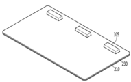
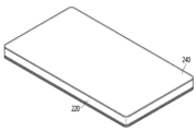
図1は発明の実施例に係る照明モジュールを示した斜視図であり、図2は図1の照明モジュールのB‐B側断面図であり、図3は図1の照明モジュールのC‐C側断面図であり、図4は図1の照明モジュールの部分平面図の例であり、図5は図1の照明モジュールの光抽出例であり、図6は図1の照明モジュールの長さを変形した例であり、図7は図1の照明モジュールの分解斜視図である。
[Lighting module]
1 is a perspective view showing a lighting module according to an embodiment of the invention, FIG. 2 is a BB side cross-sectional view of the lighting module of FIG. 1, and FIG. 3 is a CC side of the lighting module of FIG. 4 is an example of a partial plan view of the lighting module of FIG. 1, FIG. 5 is an example of light extraction of the lighting module of FIG. 1, and FIG. 6 is a modified length of the lighting module of FIG. 7 is an exploded perspective view of the lighting module of FIG.
図1~図6を参照すると、発明の実施例に係る照明モジュール200は、1つまたは複数の発光素子105を含み、前記発光素子105から放出された光をライン形態の面光源として照射することになる。前記発光素子105から放出された光は、垂直方向に一定高さを有する光源として放出される。
1 to 6, a
前記照明モジュール200は、基板210、前記基板210の上に配置された樹脂層220及び前記樹脂層220の上に配置された第2反射層240を含むことができる。前記照明モジュール200は、前記基板210と前記樹脂層220の間に第1反射層230を含むことができる。
The
図2及び図3のように、前記照明モジュール200は、第1方向Xへの長さX1が第2方向Yの幅Y1より大きい。前記第1及び第2方向X、Yの長さは、垂直な方向Zの厚さZ1または高さよりは大きい。前記第1方向の長さX1は、前記発光素子105の配置個数に応じて可変し、例えば30mm以上を有することができる。前記第2方向の幅Y1は16mm以上を有することができる。前記照明モジュール200の第2方向Yの幅Y1は、発光素子105から出射された光が拡散する領域と発光素子105の後方を保護する領域を提供することができる。前記照明モジュール200は、フレキシブルなモジュールまはたリジッド(rigid)なモジュールからなることができる。前記照明モジュール200は、第1及び第2方向X、Yの少なくとも1つに対してフラットまたはフレキシブル形成されてもよい。
As shown in FIGS. 2 and 3, the
前記照明モジュール200は、前記発光素子105と対向する前面S1と、前記前面S1の反対側の後面S2、前記前面S1と前記後面S2の両端部から第2方向に延長される複数の側面S3、S4を含むことができる。前記後面S2は、第1方向Xに延長され、前記前面S1は、前記後面S1と対向し、曲面を含むことができる。前記前面S1及び後面S2の第1方向Xの長さは、垂直方向の高さまたは厚さより大きい。前記前面S1及び後面S2の第1方向Xの最大の長さは、相互同一または異なってもよい。前記前面S1及び後面S2の垂直方向の高さまたは厚さは、同一であってもよい。前記複数の側面S3、S4は、相互対向する第1側面S3及び第2側面S4を含む。前記前面S1と前記後面S2は、第1方向Xに長い長さを有することができる。前記第1側面S3及び第2側面S4は、前記第1方向Xと直交する第2方向Yに相互対向することができる。前記前面S1は、発光素子105の出射面111と対向または前記第1側面S1と第2側面S2の第1端部から第2方向に露出した面であってもよい。前記後面S2は、複数の発光素子105の後面と対向または前記第1側面S1と第2側面S2の第2端部から第2方向に露出する面であってもよい。前記第1側面及び第2側面S3、S4は、前記前面S1と後面S2と異なる側面であってもよい。前記発光素子105の後面は、出射面111の反対側面であってもよい。
The
前記照明モジュール200の各側面S1、S2、S3、S4は、前記照明モジュール200内で最も厚い厚さを有する樹脂層220の各側面であってもよい。
Sides S1, S2, S3, and S4 of the
前記照明モジュール200において、複数の発光素子105が第1方向に配列される。前記発光素子105は、第1方向に2つ以上が配置され、例えばn個(n=2以上)であってもよい。前記複数の発光素子105は、第1方向Xに延長される直線上に配列される。前記複数の発光素子105は、1列に配列される。別の例として、前記複数の発光素子は2列に配置され、2列の素子はジグザグ形態に配列されてもよい。前記発光素子105の前面または出射面は、第2方向Yに向かって露出することができる。前記発光素子105の側面や後面は非出射面であってもよい。
In the
前記複数の発光素子105は、前記前面S1と対向することができる。前記複数の発光素子105の出射面111は、前記前面S1と対向することができる。前記発光素子105から放出された光は前面S1を通じて放出され、一部光は、前記後面S2、第1側面S3及び第2側面S4の少なくとも1つを通じて放出される。即ち、前記発光素子105から放出された殆どの光は、前面S1を通じて放出される。
The plurality of light emitting
図4のように、前記発光素子105を基準として、前記発光素子105と前面S1の間の距離D2と前記発光素子105と後面S2の間の距離D3は相互異なる。前記発光素子105と前記後面S2の間の距離D3は2mm以上を有することができ、例えば2mm~20mmの範囲を有することができる。前記発光素子105と前記後面S2の間の距離D3が前記範囲より小さいと、湿気が浸透したり回路パターンを形成できる領域が小さくなる恐れがあり、前記範囲より大きいと、照明モジュール200のサイズが大きくなる。前記距離D2は、最大距離であり、5mm以上を有することができ、5mm~20mmの範囲を有することができる。前記距離D2が前記範囲より小さいと、ホットスポットが発生する恐れがあり、前記範囲より大きいと、モジュールサイズが大きくなる。
As shown in FIG. 4, with the
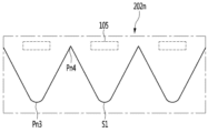
図1~図3を参照すると、前記照明モジュール200は、複数の凸部P0(P1、P2、P3)と少なくとも1つの凹部C1、C2を含むことができる。前記複数の凸部P0(P1、P2、P3)は、少なくとも2つ以上であるか、n個(n=2以上)であってもよい。前記複数の凸部P0(P1、P2、P3)は、前記複数の発光素子105が配列される第1方向に配置され、前記第1方向と直交する第2方向に凸状に突出することができる。前記複数の凸部P0(P1、P2、P3)は、前記複数の発光素子105と対向することができる。前記複数の凸部P0(P1、P2、P3)のそれぞれは、前記発光素子105(101、102、103)のそれぞれから離れる方向に突出することができる。即ち、前記凸部P0(P1、P2、P3)は、前記発光素子105の中心と対向する領域であるほど、前記発光素子105との距離が遠くなる。
1 to 3, the
前記凸部P0(P1、P2、P3)のそれぞれは、前記発光素子105のそれぞれに対して前記前面S1方向に突出することができる。前記凹部C1、C2は、前記前面S1に対して前記後面S2方向に凹むことができる。前記凸部P1、P2、P3は、凸状の曲面を含むことができる。前記凹部C1、C2は、凹んだ曲面を含むことができる。前記凸部P1、P2、P3は、第1曲率を有し、前記第2凹部C1、C2は、前記第1曲率の半径より小さい半径を有する第2曲率を有することができる。
Each of the protrusions P0 (P1, P2, P3) may protrude toward the front surface S1 with respect to each of the
前記凸部P0(P1、P2、P3)において前面S1は一定高さを有し、上面及び下面は水平な平面で提供される。前記前面S1は、第3方向Zに垂直な面で提供される。前記後面S2、第1側面S3及び第2側面S4は、第3方向に垂直な面で提供される。前記後面S2は、前記第1側面S3及び第2側面S4に対して垂直な方向に配置される。前記第3方向Zは、前記第1及び第2方向X、Yと直交する方向であってもよい。別の例として、前記前面S1は、第3方向Zに対して傾斜した面を含むことができる。前記前面S1、後面S2、第1側面S3及び第2側面S4は、前記第3方向Zに同じ厚さまたは同じ高さを有することができる。 The front surface S1 of the protrusions P0 (P1, P2, P3) has a constant height, and the upper and lower surfaces thereof are horizontal planes. The front surface S1 is provided in a plane perpendicular to the third direction Z. As shown in FIG. The rear surface S2, the first side surface S3 and the second side surface S4 are perpendicular to the third direction. The rear surface S2 is arranged in a direction perpendicular to the first side surface S3 and the second side surface S4. The third direction Z may be a direction orthogonal to the first and second directions X and Y. As another example, the front surface S1 may include a surface inclined with respect to the third direction Z. The front surface S1, the rear surface S2, the first side surface S3 and the second side surface S4 may have the same thickness or height in the third direction Z.
前記樹脂(resin)層220は、基板210と第2反射層240の間に配置される。前記樹脂層220は、前記基板210の上面と前記第2反射層240の下面の間に配置される。前記樹脂層220は、前記前面S1、前記後面S2、第1側面S3及び第2側面S4を含む。前記樹脂層220は、前記基板210の上に配置された複数の発光素子105を包むか埋めることができる。
The
前記照明モジュール200は、前記樹脂層220と前記基板210の間に第1反射層230を含むことができる。前記樹脂層220は透光性層であってもよい。前記樹脂層220は、他の材質としてガラス材質を含むことができる。
The
前記複数の発光素子105(101、102、103)は、例えば前記第1側面S3に隣接した第1発光素子101、前記第2側面S4に隣接した第3発光素子103、前記第1及び第3発光素子101、103の間に配置された少なくとも1つまたは2つ以上の第2発光素子102を含むことができる。前記発光素子は、後述されるようにn個(nは2以上)であってもよく、説明の便宜のために3個の発光素子を例として説明することにする。
The plurality of light emitting elements 105 (101, 102, 103) are, for example, the first
前記凸部P1、P2、P3は、前記第1発光素子101と対応する第1凸部P1、前記第2発光素子102と対応する第2凸部P2、及び前記第3発光素子103と対応する第3凸部P3を含むことができる。前記凹部C1、C2は、前記第1及び第2凸部P1、P2の間に配置された第1凹部C1と、前記第2及び第3凸部P2、P3の間に配置された第2凹部C2を含むことができる。前記第1~第3凸部P1、P2、P3のそれぞれは、前記第1~第3発光素子101、102、103のそれぞれの出射面111は対向することができる。
The protrusions P1, P2, and P3 correspond to the first protrusion P1 corresponding to the first
前記第1凸部P1は、前記第1発光素子101と第2方向Yに重なり、前記第2凸部P2は、前記第2発光素子102と第2方向Yに重なり、前記第3凸部P3は、前記第3発光素子103と第2方向Yに重なることができる。前記第1~第3凸部P1、P2、P3のそれぞれは、前記第1~第3発光素子101、102、103のそれぞれと第2方向に重なるように配置され、前記第1~第3発光素子101、102、103の出射面111から放出された光を拡散させることができる。このために、前記第1~第3凸部P1、P2、P3は、前記第1~第3発光素子101、102、103の各出射面111と第2方向Yに重なることができる。
The first protrusion P1 overlaps the first
前記第1~第3凸部P1、P2、P3は、第1方向に重なり、前記第1及び第2凹部C1、C2は、第1方向に重なることができる。前記凸部P0(P1、P2、P3)のうち前記発光素子105(101、102、103)と第2方向に重なった領域は、前記凹部C1、C2よりは前記凸部P0の頂点に隣接することができる。 The first to third protrusions P1, P2 and P3 may overlap in the first direction, and the first and second recesses C1 and C2 may overlap in the first direction. Regions of the protrusions P0 (P1, P2, P3) overlapping the light emitting elements 105 (101, 102, 103) in the second direction are closer to the apexes of the protrusions P0 than the recesses C1, C2. be able to.
前記第1凹部C1は、前記第1及び第2発光素子101、102の間の領域と第2方向に重なり、前記第2凹部C2は、前記第2及び第3発光素子102、103の間の領域と第2方向Yに重なることができる。前記第1及び第2凹部C1、C2は、入射される一部光を透過または反射させることができる。前記第1及び第2凹部C1、C2は、第1~第3発光素子101、102、103の間の領域における暗い部分の発生を抑制することができる。
The first recess C1 overlaps the area between the first and second
前記基板210は、印刷回路基板(PCB:Printed Circuit Board)を含み、例えば、樹脂系の印刷回路基板、メタルコア(Metal Core)PCB、フレキシブル(Flexible)PCB、セラミックPCB、またはFR‐4基板を含むことができる。前記基板210は、フレキシブルまたはインフレキシブル材質の基板であってもよい。前記基板210は、上部に回路パターンが配置される。前記基板210の回路パターンは、前記発光素子105と対応する領域に複数のパッドを備えることができる。
The
前記基板210の領域のうち、前記発光素子105を基準として後方領域は、光が出射される領域の反対側領域として、前記発光素子105を連結するための回路パターンが配置される。前記後方領域は、前記発光素子105の個数または前記発光素子105の連結方式によって幅が可変する。前記後方領域の幅は、前記発光素子105と前記後面S2の間の距離D3として、2mm以上で提供される。これによって、前記発光素子105の後方から湿気の浸透を抑制し、複数の発光素子105を連結するための回路パターンを形成することができる。
A circuit pattern for connecting the
前記複数の発光素子105は、下部にボンディング部が配置され、前記基板210のパッドと電気的に連結される。前記複数の発光素子105は、前記基板210の回路パターンによって直列に連結される。別の例として、前記複数の発光素子105は、前記基板210の回路パターンによって並列に連結されるか、2つ以上が直列に連結されたグループが並列に連結される。
The plurality of light emitting
前記発光素子105は、発光チップを有する素子またはLEDチップがパッケージングされたパッケージを含むことができる。前記発光チップは、青色、赤色、緑色、紫外線(UV)の少なくとも1つを発光することができる。前記発光素子105は、白色、青色、赤色、緑色のうち少なくとも1つを発光することができる。前記発光素子105は、側方向に光を放出し、底部が前記基板210の上に配置される。前記発光素子105は、サイドビュー(side view)タイプのパッケージであってもよい。別の例として、前記発光素子105は、LEDチップであってもよく、前記LEDチップの一面が開放され、他面は反射部材が配置される。
The
前記発光素子105の出射面111は、前記基板210に隣接した面、例えば前記基板210の上面に隣接した側面に配置される。前記出射面111は、前記発光素子105の底面と上面の間の側面に配置され、前記第2方向Yに光を放出することになる。前記発光素子105の出射面111は、前記第1反射層230に隣接し、前記基板210の上面及び前記第1反射層230の上面に対して垂直な面であってもよい。
The
前記発光素子105の厚さは、発光素子105の第1方向Xの長さより小さくてもよい。前記発光素子105の厚さは3mm以下、例えば2mm以下であってもよい。前記発光素子105の厚さは1mm~2mmの範囲であってもよく、例えば1.2mm~1.8mmの範囲を有することができる。
The thickness of the
前記発光素子105の第1方向Xの長さは、前記発光素子105の厚さより大きくてもよく、例えば前記発光素子105の厚さの1.5倍以上であってもよい。このような発光素子105は、薄い厚さと第1方向に長い長さを有することになるので、前記発光素子105の中心を基準として左右方向である第1方向Xへの光出射角を広く提供することができる。ここで、前記発光素子105の第1方向Xへの光出射角は、上下方向である第3方向Zへの光出射角より大きい。前記発光素子105の第1方向の光出射角は110度~160度の範囲を有することができる。前記発光素子105の第1方向Xの長さは、前記発光素子105の第2方向の幅より大きい。
The length of the
ここで、図2のように、前記基板210の厚さZaは、前記発光素子105の厚さより小さくてもよい。前記発光素子105の厚さは、前記基板210の厚さZaの2倍以上であってもよく、例えば2倍~4倍の範囲を有することができる。前記基板210の厚さZaが薄く提供されるので、照明モジュール200は、フレキシブルプレートとして提供される。
Here, as shown in FIG. 2, the thickness Za of the
図2~図4のように、前記樹脂層220は、前記基板210の上に配置される。前記第1反射層230は、前記樹脂層220と前記基板210の間に配置される。前記樹脂層220は、前記発光素子105を覆うことができる。前記樹脂層220は、前記発光素子105の上面と側面に接触することができる。前記樹脂層220は、前記第1反射層230の上面に接触することができる。前記樹脂層220の一部は、前記第1反射層230を通じて前記基板210に接触することができる。前記樹脂層220は、前記発光素子105の出射面111に接触することができる。前記樹脂層220の前面S1、後面S2、第1側面S3及び第2側面S4は、前記第1及び第2反射層230、240の間の側面である。前記前面S1、後面S2、第1側面S3及び第2側面S4は、前記発光素子105の周りの面であるか、前記発光素子105の側面と対応する面であってもよい。
The
前記樹脂層220の上面面積は、前記基板210の上面面積と同一であってもよい。前記樹脂層220の上面面積は、前記第1反射層230の上面面積と同一であってもよい。前記樹脂層220の上面面積は、前記第2反射層240の上面面積と同一であってもよい。第1方向に、前記樹脂層220の長さX1は、前記基板210の長さと同一であってもよい。第1方向に、前記樹脂層220の長さX1は、前記第1反射層230の長さと同一であってもよい。第1方向に、前記樹脂層220の長さX1は、前記第2反射層240の長さと同一であってもよい。第2方向に、前記樹脂層220の最大幅Y1は、前記基板210の最大幅と同一であってもよい。第2方向に、前記樹脂層220の最大幅Y1は、前記第1反射層230の最大幅と同一であってもよい。第2方向に、前記樹脂層220の最大幅Y1は、前記第2反射層240の最大幅と同一であってもよい。第2方向に、前記樹脂層220の最小幅は、前記基板210の最小幅と同一であってもよい。第2方向に、前記樹脂層220の最小幅は、前記第1反射層230の最小幅と同一であってもよい。第2方向に、前記樹脂層220の最小幅は、前記第2反射層240の最小幅と同一であってもよい。第2方向への最大幅は、照明モジュールの凸部P1、P2、P3の頂点と後面S2の間の長さであり、最小幅は、前記照明モジュールの凹部C1、C2の底点と後面S2の間の長さである。
A top surface area of the
前記樹脂層220は、第1及び第2反射層230、240の間に配置される。前記第1及び第2反射層230、240は同一面積を有し、前記樹脂層220の下面と上面で相互対向することができる。これによって、前記樹脂層220は、発光素子105から放出された光と第1及び第2反射層230、240で反射した光を拡散させて側方向にガイドすることができる。
The
前記樹脂層220は、前記発光素子105の厚さより厚い厚さZbで形成される。これによって、前記樹脂層220は、前記発光素子105の上部を保護し、湿気の浸透を防止することができる。前記発光素子105は、下部に基板210が配置され、上部に樹脂層220が配置されるので、前記発光素子105を保護することができる。よって、前記樹脂層220の上面と前記発光素子105の間の間隔は0.6mm以下、例えば0.5mm~0.6mmの範囲で配置される。前記樹脂層220の上部は、前記間隔と同じ厚さで配置され、前記発光素子105の上部を保護することができる。
The
前記樹脂層220の厚さZbは、前記樹脂層220の上面と下面の間の間隔である。前記樹脂層220の厚さZbは、前記第1及び第2反射層230、240の間の距離を有することができる。前記厚さZbは、第1及び第2反射層230、240の間の距離(例えばZb)と同一であってもよい。前記厚さZbは、前記前面S1と前記後面S2の間の距離より小さくてもよい。例えば、前記前面S1と前記後面S2の間の距離は、最大幅または最小幅を含むことができる。前記最大幅は、前記凸部P1、P2、P3の頂点と後面S2の間の直線距離を有することができる。前記樹脂層220の第1及び第2側面S3、S4の間の距離または間隔は、前記凸部P1、P2、P3の頂点と前記後面S2の間の距離より大きい。前記最小幅は、前記凹部C1、C2の底点と後面S2の間の直線距離を有することができる。前記第1反射層230と前記第2反射層240の間の距離または間隔は、前記樹脂層220の前面S1と後面S2の間の距離または間隔より小さくてもよい。このような第1及び第2反射層230、240の間の距離を照明モジュール200の第2方向の幅Y1または最小幅より小さく配置することで、ライン形態の面光源を提供し、光度改善及びホットスポットを防止することができる。また、照明モジュールは、第3方向に突出または凹むことができるフレキシブル特性を有するように提供される。
The thickness Zb of the
前記樹脂層220の厚さZbは、前記発光素子105の厚さの2倍以下であってもよく、例えば1倍以上2倍以下であってもよい。前記樹脂層220の厚さZbは、例えば1.5mm~1.9mmの範囲または1.6mm~1.8mmの範囲を有することができる。前記樹脂層220の厚さZbは、前記照明モジュール200の厚さZ1の0.8倍以下であってもよく、例えば前記照明モジュール200の厚さZ1の0.4倍~0.8倍の範囲を有することができる。前記樹脂層220が前記照明モジュール200の厚さZ1と1.2mm以下の差で配置されるので、照明モジュール200における光効率の低下を防止でき、フレキシブル特性を強化させることができる。
The thickness Zb of the
前記樹脂層220は、シリコーン、シリコーンモールディングコンパウンド(SMC)、エポキシまたはエポキシモールディングコンパウンド(EMC)のような樹脂材質を含むことができる。前記樹脂層220は、UV(ultra violet)硬化性樹脂または熱硬化性樹脂材料を含むことができ、例えばPC、OPS、PMMA、PVCなどを選択的に含むことができる。例えば、前記樹脂層220の主材料は、ウレタンアクリレートオリゴマーを主原料とする樹脂材料を利用することができる。例えば、合成オリゴマーであるウレタンアクリレートオリゴマーをポリアクリルであるポリマータイプと混合されたものを用いることができる。勿論、ここに低沸点希釈型反応性モノマーであるIBOA(isobornyl acrylate)、HPA(Hydroxylpropyl acrylate、2-HEA2-hydroxyethyl acrylate)等が混合されたモノマーをさらに含むことができ、添加剤として光開始剤(例えば、1-hydroxycyclohexyl phenyl-ketoneなど)または酸化防止剤などを混合することができる。
The
前記樹脂層220内にはビーズ(bead、図示されない)を含むことができ、前記ビーズは入射される光を拡散及び反射させ、光量を増加させることができる。前記樹脂層220は蛍光体を含むことができる。前記蛍光体は、黄色蛍光体、緑色蛍光体、青色蛍光体、赤色蛍光体の少なくとも1つを含むことができる。
The
前記樹脂層220において、前記凸部P1、P2、P3が形成された領域はレンズ部として提供される。前記樹脂層220のレンズ部は、凸状の曲面を有するレンズ形状で提供され、トップビューで見ると半球形状を含むことができる。前記レンズ部は、前記発光素子105の中心と対応する領域であるほど、前記発光素子105との距離がより離隔される。前記レンズ部の第3方向の厚さは、前記樹脂層220の厚さZbであってもよい。このようなレンズ部は、上面及び下面が平坦であり、前面S1方向に曲面で形成されるので、前面S1方向に入射された光を拡散させることができる。前記レンズ部は、上部及び下部に平坦な第1及び第2反射層230、240の間に配置され、前面S1に光を屈折させて出射することができる。前記レンズ部は、光軸を基準として、前記光軸をはずれた領域に入射される光を入射角より大きい出射角で光を屈折させることができる。
In the
前記樹脂層220において、前記凸部P1、P2、P3の間に配置された凹部C1、C2は、後面S2方向に凹んだリセス(Recess)として提供され、前記リセスは、前記凹んだ曲面または変曲点を有する曲面を含むことができる。前記樹脂層220のリセスは、前記樹脂層220の表面から凹んだ曲面で形成され、入射された光を屈折させることができる。このような凹部C1、C2のリセスは、前記レンズ部の間の領域で発光素子105から放出された光を屈折させ、暗い部分の発生を抑制することができる。
In the
ここで、前記樹脂層220に凸部P1、P2、P3及び前記凹部C1、C2が配置された場合、前記基板210と前記第1及び第2反射層230、240は、前記凸部と凹部に対応する形状が形成される。前記樹脂層220の凸部P1、P2、P3またはレンズ部は、前記発光素子105の個数と同一であってもよい。
Here, when the convex portions P1, P2, P3 and the concave portions C1, C2 are arranged on the
前記第1反射層230は、前記発光素子105から放出された光を反射させることができる。前記第1反射層230は、前記基板210の上面に形成される。前記第1反射層230は、前記基板210の上部層として形成されるか別途の層として形成される。前記第1反射層230は、前記基板210の上面に接着剤で接着される。前記第1反射層230の上面は、前記樹脂層220が接着される。
The first
前記第1反射層230は、前記発光素子105の下面と対応する領域に複数の孔232を備え、前記孔232を通じて前記発光素子105が前記基板210に連結される。前記樹脂層220の一部は、前記孔232を通じて前記基板210に接触することができる。前記孔232は、前記発光素子105が前記基板210にボンディングされる領域であってもよい。
The first
前記第1反射層230は、単層または多層構造に形成される。前記第1反射層230は、光を反射する物質、例えば金属または非金属物質を含むことができる。前記第1反射層230が金属である場合、ステンレス、アルミニウム(Al)、銀(Ag)のような金属層を含むことができ、非金属物質である場合、白色樹脂材質やプラスチック材質を含むことができる。前記第1反射層230は、白色樹脂材質やポリエステル(PET)材質を含むことができる。前記第1反射層230は、低反射フィルム、高反射フィルム、乱反射フィルムまたは正反射フィルムのうち少なくとも1つを含むことができる。前記第1反射層230は、例えば入射された光を前面S1に反射させるための正反射フィルムにて提供される。
The first
前記第1反射層230の厚さZcは、前記基板210の厚さZaより小さくてもよい。前記第1反射層230の厚さZcは、前記基板210の厚さZaの0.5倍以上で配置され、入射される光の透過損失を減らすことができる。前記第1反射層230の厚さZcは0.2mm~0.4mmの範囲であってもよく、前記範囲より小さい場合、光透過損失が発生することがあり、前記範囲より厚い場合、照明モジュール200の厚さZ1が増加することになる。
The thickness Zc of the first
前記第2反射層240は、前記樹脂層220の上に配置される。前記第2反射層240は、前記樹脂層220の上面に接着される。前記第2反射層240は、前記樹脂層220の上面全領域に配置され、光の損失を減らすことができる。
The second
前記第2反射層240は、前記第1反射層230と同じ材質であってもよい。前記第2反射層240は、光を反射し光の透過損失を減らすために、前記第1反射層230の材質より光反射率が高い材質であるかより厚い厚さを有することができる。前記第2反射層240は、前記第1反射層230と同じまたはより厚い厚さを有することができる。例えば、前記第1及び第2反射層230、240は同じ材質及び同じ厚さで提供される。
The second
前記第2反射層240の厚さZdは、前記基板210の厚さZaより小さくてもよい。前記第2反射層240の厚さZdは、前記基板210の厚さZaの0.5倍以上で配置され、入射される光の透過損失を減らすことができる。前記第2反射層240の厚さZdは0.2mm~0.4mmの範囲であってもよく、前記範囲より小さい場合、光透過損失が発生することがあり、前記範囲より厚い場合、照明モジュール200の厚さZ1が増加することになる。
The thickness Zd of the second
前記第2反射層240は、単層または多層構造に形成される。前記第2反射層240は、光を反射する物質、例えば金属または非金属物質を含むことができる。前記第2反射層240が金属である場合、ステンレス、アルミニウム(Al)、銀(Ag)のような金属層を含むことができ、非金属物質である場合、白色樹脂材質やプラスチック材質を含むことができる。前記第2反射層240は、白色樹脂材質やポリエステル(PET)材質を含むことができる。前記第2反射層240は、低反射フィルム、高反射フィルム、乱反射フィルムまたは正反射フィルムのうち少なくとも1つを含むことができる。前記第2反射層240は、例えば入射された光が前面S1方向に進行するように正反射フィルムにて提供される。
The second
前記基板210、前記第1反射層230、前記樹脂層220及び前記第2反射層240の積層構造は、前記凸部P1、P2、P3と前記凹部C1、C2を含むことができる。前記凸部P1、P2、P3は、上面と下面が平坦な形状であり、第1方向に曲面または半球形状を含むことができる。前記凹部C1、C2は後面S2方向に前記凹んだ曲面を含むことができる。
A stack structure of the
前記樹脂層220での前記突出した曲面及び前記凹んだ曲面は、ヘイズ(Haze)面となるように処理され、光を拡散させることができる。前記ヘイズ面は、前記樹脂層220の内部面をよりラフな面となるように処理され、出射される光を拡散させることができる。
The protruded curved surface and the recessed curved surface of the
発明の実施例に係る照明モジュール200は、第3方向の厚さZ1をライン形態に提供して、フレキシブルを有し、ライン形態の面光源を提供することができる。前記照明モジュール200の厚さZ1は3mm以下であってもよい。即ち、前記照明モジュール200は、3mm以下のライン形態の面光源として提供される。別の例として、前記照明モジュール200は、3mm以上6mm以下に配置され、この場合、照明モジュール200の厚さは増加するが、樹脂層220の厚さをより厚く提供してライン幅を増加させ、配光領域を増加させることができる。
The
図2を参照すると、前記照明モジュール200において、各構成要素の厚さを見ると、基板210の厚さはZaであり、樹脂層220の厚さはZbであり、第1反射層230の厚さはZcであり、第2反射層240の厚さはZdである場合、Zb>Za>Zd≧Zcの関係を有することができる。前記基板210の下面で前記第2反射層240の上面の間の間隔は、照明モジュール200の厚さZ1である。前記厚さZbはZ1の0.4~0.8の比率であり、前記厚さZaはZ1の0.14~0.18の比率であり、前記厚さZdまたはZcは0.08~0.12の比率を有することができる。前記ZbはZaの3.5~4の比率を有することができる。前記ZbはZcまたはZdの5.8~6.4の比率を有することができる。このような樹脂層220の厚さZbを基板210の厚さZaより厚く配置して、発光素子105を保護し、光を拡散させてガイドすることができ、フレキシブル特性を強化させることができる。
Referring to FIG. 2, when looking at the thickness of each component in the
図4を参照すると、第1方向への前記凸部P1、P2、P3の最大幅W1は、前記隣接した凹部C1、C2の間の距離として、前記発光素子105のピーチG1と同一またはより小さくてもよい。前記凸部P1、P2、P3の最大幅W1が前記発光素子105の間のピーチG1より大きい場合、前記凸部P1、P2、P3の領域に2つ以上の発光素子105が配置されることができ、光度を増加させることができる。前記凸部P1、P2、P3の最大幅W1が前記発光素子105の間のピーチG1より小さい場合、凸部P1、P2、P3の大きさが小さいので光の均一な分布を提供することができるが、光度は減少することになる。
Referring to FIG. 4, the maximum width W1 of the protrusions P1, P2, P3 in the first direction is equal to or smaller than the pitch G1 of the
前記凸部P1、P2、P3の最大幅W1は15mm以上、例えば15mm~20mmの範囲を有することができる。前記凸部P1、P2、P3の最大幅W1は、前記凹部C1、C2の深さD4よりは大きい。前記凸部P1、P2、P3の最大幅Wと前記凹部C1、C2の深さD4の比率は、1:0.4~1:0.7の範囲を有することができる。前記凹部C1、C2の深さが前記範囲より小さい場合、隣接した凸部P1、P2、P3の間で暗い領域が増加することになる。前記凹部C1、C2の深さが前記範囲より大きい場合、前記発光素子105に隣接した領域まで進行して発光素子105の間の光干渉が増加することになる。前記凹部C1、C2の深さD4は、前記凸部P1、P2、P3の頂点を連結した直線から前記凹部C1、C2の底点の間の直線距離を有することができる。
The maximum width W1 of the protrusions P1, P2, P3 may be 15 mm or more, for example, in the range of 15 mm to 20 mm. The maximum width W1 of the protrusions P1, P2, P3 is greater than the depth D4 of the recesses C1, C2. A ratio of the maximum width W of the protrusions P1, P2, P3 and the depth D4 of the recesses C1, C2 may range from 1:0.4 to 1:0.7. If the depths of the recesses C1 and C2 are smaller than the range, dark areas will increase between the adjacent protrusions P1, P2 and P3. If the depths of the recesses C1 and C2 are greater than the range, the light travels to areas adjacent to the
前記凸部P1、P2、P3の曲面と前記凹部C1、C2の曲面は、曲率を有することができる。前記凸部P1、P2、P3の曲率半径は8mm以上、例えば8mm~14mmの範囲または9mm~11mmの範囲を有することができる。前記凸部P1、P2、P3の曲率半径が前記範囲より小さい場合、光度の改善が微小となり、前記範囲より大きい場合、暗い部分が発生することになる。 The curved surfaces of the protrusions P1, P2 and P3 and the curved surfaces of the recesses C1 and C2 may have a curvature. The radius of curvature of the protrusions P1, P2, P3 may be 8 mm or more, eg, in the range of 8 mm to 14 mm or in the range of 9 mm to 11 mm. If the radii of curvature of the protrusions P1, P2, and P3 are smaller than the range, the improvement in luminous intensity will be small, and if they are larger than the range, dark areas will occur.
前記凹部C1、C2の曲率半径は、前記凸部P1、P2、P3の曲率半径より1/8倍小さくてもよい。前記凹部C1、C2の曲率半径と前記凸部P1、P2、P3の曲率半径の比率は、1:8~1:28の範囲を有することができる。前記凹部C1、C2の曲率半径が前記範囲より小さい場合、前記凹部C1、C2を通じて放出される光量が減り暗い部分が増加し、前記範囲より大きい場合、前記凸部P1、P2、P3のサイズが小さくなる恐れがあり、前記発光素子105の間の光干渉が発生することになる。よって、前記凹部C1、C2の深さD4及び曲率半径は、前記発光素子105の位置及び前記発光素子105の指向角を考慮して、前記凸部P1、P2、P3及び前記凹部C1、C2を通じた光の均一度改善と前記凹部C1、C2における暗い部分を抑制のための範囲を有することができる。前記凹部C1、C2の曲率半径は、0.5~1mmの範囲を有することができる。前記凹部C1、C2が所定曲率を有し、曲面形状で提供されることで、入射される光を屈折させて透過させることができ、前記凹部C1、C2領域における暗い部分の発生を減らすことができる。
The radius of curvature of the recesses C1, C2 may be ⅛ times smaller than the radius of curvature of the protrusions P1, P2, P3. A ratio of the radius of curvature of the concave portions C1 and C2 to the radius of curvature of the convex portions P1, P2 and P3 may range from 1:8 to 1:28. When the radius of curvature of the recesses C1 and C2 is smaller than the range, the amount of light emitted through the recesses C1 and C2 is reduced and the dark portion increases. There is a possibility that the
前記凸部P1、P2、P3の頂点と前記発光素子105の間の領域は、光を拡散させて均一な光分布で放出するための領域として、光拡散領域または導光領域と定義することができる。前記凸部P1、P2、P3の頂点と前記発光素子105の間の間隔は13mm以上であり、例えば13mm~20mmの範囲を有することができる。前記凸部P1、P2、P3の頂点と前記発光素子105の間の間隔は、前記範囲である時、光拡散を通じて均一な分布で提供され、前記凸部P1、P2、P3と前記発光素子105の間の間隔が前記範囲より小さい場合、ホットスポットが発生する恐れがあり、前記範囲より大きい場合、光度が低下し、モジュールのサイズが増加することになる。前記凸部P1、P2、P3と前記発光素子105の間の間隔は、前記凸部P1、P2、P3の曲率半径よりは大きくてもよく、例えば前記凸部P1、P2、P3の曲率半径の1.3倍以上または1.3倍~2.0倍の範囲を有することができる。
A region between the apexes of the protrusions P1, P2, and P3 and the
前記凹部C1、C2は、前記発光素子105を連結する直線の間の間隔D1が前記凹部C1、C2の深さD4よりは小さくてもよい。前記間隔D1は5mm以上、例えば5mm~12mmの範囲であってもよく、前記間隔D1より小さい場合、前記凹部C1、C2の深さD4が深くなったり発光素子105と凸部P1、P2、P3の間の距離D2が狭くなり、前記凹部C1、C2で暗い部分の発生または前記凸部P1、P2、P3でホットスポットが発生することになる。
In the recesses C1 and C2, a distance D1 between straight lines connecting the
図5を参照すると、発光素子105から出射された光のうち光軸方向に進行する光L1は、凸部P1、P2、P3の中心を透過することになり、前記光軸周辺に出射された光L2は、入射角より大きい出射角で放出され、光を拡散させることができる。また、凹部C1、C2に入射された光L3は屈折されて透過したり凸部P1、P2、P3によって反射されて出射され、凹部C1、C2における暗い部分の発生を減らすことができる。即ち、図37のように、発明の実施例に係る照明モジュールは、(a)のような放出された光度分布において暗い領域Rbが明るい領域Raより小さく現れ、(b)のように等光度曲線分布を有することができる。図38は、発明の実施例に係る照明モジュールにおいて凸部と凹部がないフラットな前面を有する構造として、図15のようなモジュールとして提供され、光度分布において明るい領域Raより暗い領域Rbが大きくなり、(b)のような等光度曲線分布を有するようになる。
Referring to FIG. 5, of the light emitted from the
図6を参照すると、前記発光素子105の中心と凸部P0の中心を通る直線を基準として、前記発光素子105の中心と前記凹部C0の底点の間の角度R0は50度以上、例えば50度~80度の範囲を有することができる。このような前記凹部C0は、上記角度R0で離隔することで、前記発光素子105から入射される光を屈折させて外部に放出することができる。前記凸部P0と凹部C0は、図1~図5に開示された凸部P1、P2、P3と凹部C1、C2を含むことができる。
Referring to FIG. 6, the angle R0 between the center of the
図7は発明の実施例に係る照明モジュールの分解斜視図であり、図8~図13は発明の実施例に係る照明モジュールの製造過程を説明した図面である。照明モジュールの説明において、上記した構成と同じ部分は、上記説明を参照することにする。 FIG. 7 is an exploded perspective view of a lighting module according to an embodiment of the invention, and FIGS. 8 to 13 are drawings for explaining a manufacturing process of the lighting module according to an embodiment of the invention. In the description of the lighting module, the same description as that of the configuration described above will be referred to.
図7及び図8を参照すると、基板210の上に、2つ以上の発光素子105が第1方向に配列される。前記基板210の上に配置される発光素子105は、前面または前面方向に光を放出するように配置される。別の例として、前記基板210の上に発光素子105を1つの列で配列したが、2列で配列してもよく、これに限定されるものではない。
7 and 8, two or more light emitting
図7及び図9を参照すると、予め用意された第1反射層230を前記基板210の上に付着することになる。前記第1反射層230には、前記発光素子105が挿入される孔232が形成される。前記第1反射層230は、前記発光素子105の周りに配置され、前記基板210に付着されて、前記発光素子105から放出された光を反射することができる。前記第1反射層230は、前記基板210の上に反射材質のレジスト材質が配置された場合形成しなくてもよく、これに限定されるものではない。前記第1反射層230は、前記発光素子105の厚さより薄い厚さであり、前記発光素子105の出射面より下に配置される。前記第1反射層230は、プラスチック材質や、金属または非金属材質であってもよい。
Referring to FIGS. 7 and 9, a prepared first
図7及び図10を参照すると、前記第1反射層230の上に樹脂層220が形成される。前記樹脂層220は、前記第1反射層230と前記発光素子105の上にモールディングされる。前記樹脂層220は、前記発光素子105を覆うことができる厚さで形成される。前記樹脂層220は、透明な樹脂材質で形成され、例えばシリコーン、シリコーンモールディングコンパウンド、エポキシまたはエポキシモールディングコンパウンド、UV硬化性樹脂または熱硬化性樹脂のような材質であってもよい。
7 and 10, a
前記樹脂層220は、前記発光素子105の厚さより厚い厚さで提供され、前記発光素子105の厚さの2倍以下、例えば1.5倍以下に配置される。前記樹脂層220はディスフェンシング工程により形成されてもよい。
The
図7及び図11を参照すると、前記樹脂層220が硬化する前に前記樹脂層220の上面に第2反射層240が形成される。前記第2反射層240は、前記樹脂層220の上面全体を覆うことができる。前記第2反射層240は、別の例として、前記樹脂層220が硬化した後接着剤を利用して付着することができる。
7 and 11, a second
図7及び図12を参照すると、前記第2反射層240が形成されると、前記基板210から前記第2反射層240までの構造物をカッティング装備を利用して、図1、図12及び図13のようにカッティングすることになる。ここで、前記カッティング装備は、ルータ(Router)でカッティングすることができ、前記カッティング時照明モジュールの凸部P0及び凹部P0が形成させる。
7 and 12, after the second
これによって、前記照明モジュールは、前記樹脂層220の前面S1と、前記基板210の前面S1が同じ垂直平面上に配置される。また、前記樹脂層220が前面S1と前記第1反射層230及び前記第2反射層240が同じ垂直平面上に配置される。前記樹脂層220の後面S2、第1側面S3及び第2側面S4のそれぞれは、前記基板210の後面、第1側面及び第2側面それぞれと同じ垂直平面上に配置される。前記樹脂層220の後面S2、第1側面S3及び第2側面S4のそれぞれは、前記第1及び第2反射層230、240の後面、第1側面及び第2側面と同じ垂直平面上に配置される。
Accordingly, in the lighting module, the front surface S1 of the
これによって、図7、図12及び図13のように、前記照明モジュールは、前記発光素子105から放出された光が前記樹脂層220の前面S1を通じて放出される。前記樹脂層220の後面S2、第1側面S3及び第2側面S4には、内部で反射された一部光が放出される。
7, 12 and 13, the lighting module emits light from the
図14は、発明の照明モジュールの別の例である。図14のように、第1反射層230は、前記基板210のエッジから離隔し、前記樹脂層220の一部222は、前記基板210のエッジ側の上面に接触することができる。前記樹脂層220が前記基板210のエッジに接触した場合、水分の浸透を抑制することができる。
FIG. 14 is another example of an inventive lighting module. As shown in FIG. 14 , the first
別の例として、図2及び図14のような照明モジュールにおいて、前記樹脂層220の側面のうち前面S1を除いた面(S2、S3、S4)に第3反射層245がさらに配置される。前記第3反射層245は、光の漏洩を防止し、前面S1から抽出される光量を増加させることができる。前記第3反射層245は、上記に開示された第1及び第2反射層230、240の材質であってもよい。前記第3反射層245は、前記樹脂層220の側面に接触または離隔することができる。
As another example, in the lighting module of FIGS. 2 and 14, the third
以下の説明では、図3及び図7のような照明モジュールの積層構造を有し、前記照明モジュールにおける光度低下の変数を考慮して、上記に開示された構成を部分的に変更した構成である。以下の説明では、各構成の変更された部分を中心に説明することにして、上記した構成を選択的に適用することができる。 In the following description, the structure disclosed above is partially modified in consideration of the variable of luminous intensity reduction in the lighting module having a laminated structure of the lighting module as shown in FIGS. 3 and 7. . In the following description, the changed parts of each configuration will be mainly described, and the above configurations can be selectively applied.
図15は、上記に開示された照明モジュールで凸部及び凹部がないフラットな前面S1を提供した構造である。このような照明モジュールは、図7の構造で積層される。図15のような照明モジュールの水平及び垂直方向における光度は低くなり、凸部及び凹部がないので図38のように暗い部分が明るい部分より大きくなる。この場合、樹脂層の内部に拡散剤を添加してホットスポットを防止したり導光距離をより長く提供することができる。 FIG. 15 shows the structure of the illumination module disclosed above, which provides a flat front surface S1 without protrusions and recesses. Such lighting modules are stacked in the structure of FIG. The luminous intensity in the horizontal and vertical directions of the illumination module as shown in FIG. 15 is low, and since there are no protrusions and recesses, the dark areas are larger than the bright areas as shown in FIG. In this case, a diffusing agent may be added to the inside of the resin layer to prevent hot spots or provide a longer light guide distance.
図16~19は、発明の実施例に係る照明モジュールにおいて、凸部の曲率を変更した例である。図16の照明モジュール201aは、発光素子105と対応する凸部Pa1の曲率半径が5±0.5mmであり、この場合水平及び垂直方向における光度は7.5cd以下に現れる。この場合凸部Pa1と凸部Pa1の間の領域Pb2がフラットな面で対向的に提供され、光度改善に限界がある。
16 to 19 show examples in which the curvature of the convex portion is changed in the lighting module according to the embodiment of the invention. In the
図17~図19は、発明の照明モジュール201bにおいて、発光素子105と対応する凸部Pb1、Pc1、Pd1の曲率半径を漸増させた構造である。図17は凸部Pb1の曲率半径が8mm~11mmの範囲であり、図18は凸部Pc1の曲率半径が11mm~14mmの範囲であり、図19は凸部Pd1の曲率半径が15mm~21mmの範囲である。この時、図17及び図18のような構造においては、水平及び垂直方向における光度は8.5cd以上であり、図19においては、水平及び垂直方向における光度は7.5cd以上8.2cdと再び減少することがわかる。よって、発明の照明モジュールが7.5cd以上の光度で提供する場合、上記曲率半径を選択的に適用することができ、最高の光度を有するようにする場合、前記凸部Pb1、Pc1、Pd1の曲率半径が8mm~14mmの範囲で提供され、この時の凸部Pb1、Pc1、Pd1の曲率半径によって、前記凸部Pb1、Pc1、Pd1の間の領域では凹部Pb2、Pc2、Pd2が曲線なしに提供されるか0.5mm~1mmの曲率半径を有することができる。このような照明モジュールの凸部Pb1、Pc1、Pd1と凹部Pb2、Pc2、Pd2が交互に配置され、前記凸部Pが前記発光素子105と第2方向に重なって入射された光を拡散させて抽出し、前記凹部Pb2、Pc2、Pd2が入射された光を屈折させて、ライン形態の面光源の光度を改善させることができ、ホットスポットを防止することができる。ここで、前記光度は、前記発光素子105と前面S1の間の距離が13mmであり、前記照明モジュールとインナーレンズ(inner lens)の間のエアギャップ(air gap)が11mmである条件で測定した。
17 to 19 show structures in which the radii of curvature of the projections Pb1, Pc1, and Pd1 corresponding to the
図20~図34は、発明の照明モジュールにおいて前面S1の形状を変形した例である。このような変形例では、上記に開示された凸部と凹部が曲率を有する場合、水平及び垂直方向における光度より低い光度を有することができる。 20 to 34 show examples in which the shape of the front surface S1 is modified in the lighting module of the invention. In such variations, if the convex and concave portions disclosed above have a curvature, they can have a lower luminous intensity than in the horizontal and vertical directions.
図20のように、照明モジュール202aの前面S1には、凸部Pa3と凹部Pa4が交互に配置され、前記凸部Pa3は、発光素子105と重なるように配置され、前記凸部Pa3の間に凹部Pa4が所定曲率を有するように配置される。前記凸部Pa3は凸状の曲面を有し、前記発光素子105の中心部に対応するほど凹んだ曲面を有するリセスで提供される。
As shown in FIG. 20, on the front surface S1 of the
図21のように、照明モジュール202bの前面S1には、凸部Pb3と凹部Pb4が交互に配置され、前記凸部Pb3は、発光素子105と重なるように配置され、前記凸部Pb3の間に凹部Pb4がフラットな面で提供される。前記凸部Pb3は凸状の曲面を有し、前記発光素子105の中心部に対応するほど凹んだ曲面を有するリセスで提供される。前記凹部Pb4のフラットな面(または底点)は、前記発光素子105の間の領域に配置される。
As shown in FIG. 21, on the front surface S1 of the
図22のように、照明モジュール202cの前面S1には、凸部Pc3と凹部Pc4が交互に配置され、前記凸部Pc3の最大幅は、前記発光素子105の第1方向の長さより小さく配列される。よって、前記発光素子105と重なる2つ以上の凸部Pc3が配列される。このような凸部Pc3の間には凹部Pc4が配置され、前記凹部Pc4は、負の曲率を有する曲面、または変曲点または界面を有する構造に配置される。前記凸部Pc3は、前記発光素子105と13mm以上離隔される。このような場合凸部Pc3の大きさがマイクロレンズとして配列されるので、光の均一な分布を提供することができるが光度低下が発生することになる。
As shown in FIG. 22, convex portions Pc3 and concave portions Pc4 are alternately arranged on the front surface S1 of the
図23~図25は、照明モジュール202dの前面S1には凸部Pd3、Pe3、Pf3と凹部Pd4、Pe4、Pf4が交互に配置され、前記凸部Pd3、Pe3、Pf3は、前記凹部Pd4、Pe4、Pf4の底点から三角形状、例えば直角三角形状で突出することができる。前記凹部Pd4、Pe4、Pf4の底点は、前記発光素子105の出射面外側エッジ部分と対応することができる。前記凸部Pd3、Pe3、Pf3は、隣接した発光素子105の間に傾斜した面を提供することができ、前記凹部Pd4、Pe4、Pf4の底点と対応する部分は、前記底点に垂直な面で提供される。図23は、前記凸部Pd3の傾斜した面がフラットな面であり、前記凸部Pd3の頂点部分が角ばった面であり、図24は、前記凸部Pe3の頂点部分が曲面を有し、図25は、前記凸部Pf3の傾斜した面にマイクロレンズで配列される。このような図23~図25には、前記凸部Pd3、Pe3、Pf3の傾斜した方向に沿って光が透過するので、前記発光素子105を中心に等光度曲線の分布が前記傾斜した方向に長く形成される。
23 to 25, projections Pd3, Pe3, Pf3 and recesses Pd4, Pe4, Pf4 are alternately arranged on the front surface S1 of the
図26~図28は、照明モジュールの別の例である。 Figures 26-28 are another example of a lighting module.
図26を参照すると、照明モジュール202gは、前面S1で凸部Pg3と凹部Pg4が交互に配置され、前記凸部Pg3は、発光素子105と重なって突出した曲面を有し、前記凹部Pg4は、前記発光素子105の間に底点が位置することになる。このような構造においては、等光度曲線の分布を広く提供することができる。
Referring to FIG. 26, the
図27を参照すると、照明モジュール202hは、前面S1で凸部Ph3と凹部Ph4が交互に配置され、前記凹部Ph4は、多角形形状を有し、前記発光素子105と対応するように配置され、前記凸部Ph3は、前記発光素子105の間の領域に突出することができる。このような構造においては、等光度曲線の分布を広く提供することができる。
Referring to FIG. 27, the
図28を参照すると、照明モジュール202iは、前面S1で凸部Pi3と凹部Pi4が交互に配置され、前記凸部Pi3は、前記発光素子105と対応し、前記凹部Pi3は、前記発光素子105の間の領域と対応することができる。前記凸部Pi3と前記凹部Pi4は、曲面を有し、サイン波形状に提供される。このような構造においては、等光度曲線の分布を広く提供することができる。
Referring to FIG. 28, the lighting module 202i has convex portions Pi3 and concave portions Pi4 alternately arranged on the front surface S1, the convex portions Pi3 corresponding to the
図29を参照すると、照明モジュール202jは、前面S1で凸部Pj3と凹部Pj4が交互に配置され、前記凸部Pj3は、凸状の曲面を有し、前記凹部Pj4の凹んだ曲面の幅や曲率半径より小さくてもよい。このような凹部Pj4は、1つ以上が前記発光素子105と対応するように配置され、凹状のマイクロレンズ形態で提供され、等光度曲線の分布を広く提供することができる。
Referring to FIG. 29, the
図30を参照すると、照明モジュール202kは、前面S1で凸部Pk3と凹部Pk4が交互に配置され、前記凸部Pk3はフラットな面で提供され、前記発光素子105と対応し、前記凹部Pk4は、前記発光素子105の間の領域と台形形状を有し、対応することができる。前記凹部Pk4は深くなるほど幅が漸減する。このような凹部Pk4は、側面が傾斜した面で提供されるので、入射された光を屈折させることができる。
Referring to FIG. 30, a
図31を参照すると、照明モジュール202lは、図20の構造と異なるように提供される。前記照明モジュール202lは、凸部Pl3の間の凹部Pl4の深さがより深い構造であり、前記凹部Pl4の底点が前記発光素子105後面より深く配置される。このような場合、前記発光素子105の後方に進行する一部光を屈折させて前面S1に抽出させることができる。
Referring to FIG. 31, the lighting module 202l is provided differently than the structure of FIG. The illumination module 202l has a structure in which the depth of the recesses Pl4 between the protrusions Pl3 is deeper, and the bottom point of the recesses Pl4 is arranged deeper than the rear surface of the
図32~図34において、照明モジュール202m、202n、202oは、三角形状の凸部Pm3、Pn3、Po3と凹部Pm4、Pn4、Po4が配置され、図32は凹部Pm4が発光素子105の間に位置し、凸部Pm3の頂点部分は、前記発光素子105の中心と対応するように角ばった面に形成され、図33は、図32で凸部Pn4の頂点は、発光素子105の中心と対応するように曲面に形成され、図34は凹部Po4の底点が発光素子105の中心と対応するように配置され、角ばった面まはた曲面であってもよく、凸部Po3の頂点が発光素子105の間の領域と対応し、角ばった面まはは曲面であってもよい。図32及び図34のような構造においては、等光度曲線分布は広くなり、図33の場合は光度が改善される。
32 to 34,
図35及び図36は、発明の照明モジュールにおいて、発光素子105と凸部の頂点の間の距離D11、D12を図4と異なるようにした場合である。この場合、凸部P0と凹部C0は、図4の曲率を有することができる。
FIGS. 35 and 36 show the lighting module of the invention in which the distances D11 and D12 between the light emitting
図35の照明モジュール203は、発光素子105と凸部P0の頂点の間の距離D11が4~6mmである場合であり、図36は、発光素子105と凸部P0の頂点の間の距離D12が13mm~21mmの範囲であり、図35の構造よりは水平及び垂直方向における光度が高く現れるが、光度が低いこともある。図35の構造においては、導光距離が短いのでホットスポットが発生することがある。
The
また、発明の実施例は、樹脂層220の厚さを厚く提供する場合、例えば3mm~6mmに提供する場合、樹脂層220の厚さ増加によって発光面積が増加して配光分布が改善される。
In addition, according to the embodiment of the present invention, when the
発明の実施例に係る照明モジュールは、図39のようにランプに適用することができる。前記ランプは、車両用ランプの例として、ヘッドライト、車幅灯、サイドミラー灯、フォグランプ、尾灯(Tail lamp)、制動灯、昼間走行灯、車両室内照明、ドアスカーフ(door scarf)、リアコンビネーションランプまたはバックアップランプに適用可能である。 A lighting module according to an embodiment of the invention can be applied to a lamp as shown in FIG. Examples of the lamps for vehicles include headlights, width lights, side mirror lights, fog lights, tail lights, brake lights, daytime running lights, vehicle interior lighting, door scarfs, and rear combination lights. Applicable to lamps or backup lamps.
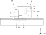
図39を参照すると、ランプは、インナーレンズ(Inner lens)502を有するハウジング503内部に、上記に開示された照明モジュール200が結合される。前記照明モジュール200の厚さは、前記ハウジング503の内部幅に挿入できる程度である。前記インナーレンズ502の出射部515の幅Z3は、前記照明モジュール200の厚さと同じであるか2倍以下であってもよいので、光度低下を防止することができる。
Referring to FIG. 39, the lamp is coupled with the
前記インナーレンズ502は、前記照明モジュール200の前面から所定距離、例えば10mm以上離隔される。前記インナーレンズ502の出射側には、アウターレンズ501が配置される。このような照明モジュール200を有するランプは一例であり、他のランプに、フレキシブルな構造、例えば側面から見て曲面または曲線型構造で適用されてもよい。
The
図40は発明の実施例に係る照明モジュールに適用された発光素子の一例を示した平面図であり、図41は図40の発光素子が回路基板に配置されたモジュールの例であり、図42は図41の他側から見たモジュールの図面である。 40 is a plan view showing an example of a light emitting element applied to a lighting module according to an embodiment of the invention, FIG. 41 is an example of a module in which the light emitting element of FIG. 40 is arranged on a circuit board, and FIG. 42 is a view of the module seen from the other side of FIG. 41; FIG.
図40を参照すると、発光素子100は、キャビティ20を有する本体10、前記キャビティ20内に複数のリードフレーム30、40、及び前記複数のリードフレーム30、40の少なくとも1つの上に配置された1つまたは複数の発光チップ71を含む。このような発光素子100は、上記実施例に開示された発光素子の一例であり、側面発光型パッケージとして具現される。
Referring to FIG. 40, the
前記発光素子100は、第1方向の長さが第2方向の幅より3倍以上、例えば4倍以上であってもよい。前記第1方向の長さは2.5mm以上、例えば2.7mm~4.5mmの範囲を有することができる。前記発光素子100は、第1方向の長さを長く提供することで、第1方向に前記発光素子100の個数を減らすことができる。前記発光素子100は、厚さを相対的に薄く提供することができ、前記発光素子100を有する照明モジュールの厚さを減らすことができる。前記発光素子100の厚さは2mm以下であってもよい。前記本体10は、キャビティ20を備え、第1方向の長さが前記本体10の厚さT1に比べて3倍以上であってもよく、第1方向の光の指向角を広めることができる。
The length in the first direction of the
前記本体10のキャビティ20の底には、リードフレーム30、40が配置される。前記前記本体10には、例えば第1リードフレーム30、及び第2リードフレーム40が結合される。
Lead frames 30 and 40 are arranged at the bottom of the
前記本体10は絶縁材質で形成されてもよい。前記本体10は反射材質で形成されてもよい。前記本体10は、発光チップから放出された波長に対して、反射率が透過率より高い物質、例えば70%以上の反射率を有する材質で形成されてもよい。前記本体10は、反射率が70%以上である場合、非透光性の材質または反射材質と定義することができる。前記本体10は、樹脂系の絶縁物質、例えばPPA(Polyphthalamide)のような樹脂材質で形成されてもよい。前記本体10は、シリコーン系またはエポキシ系またはプラスチック材質を含む熱硬化性樹脂または高耐熱性、高耐光性の材質で形成されてもよい。前記本体10は白色系の樹脂を含む。前記本体10内には、酸無水物、酸化防止剤、離型剤、光反射材、無機充電材、硬化触媒、光安定剤、潤滑剤、二酸化チタンから選択的に添加される。前記本体10は、エポキシ樹脂、変性エポキシ樹脂、シリコーン樹脂、変性シリコーン樹脂、アクリル樹脂、ウレタン樹脂からなる群から選択される少なくとも1種によって成型される。例えば、TGIC(triglycidylisocyanurate)、水素化ビスフェノールAジグリシジルエーテルなどからなるエポキシ樹脂と、ヘキサヒドロ無数フタル酸、3‐メチルヘキサヒドロ無数フタル酸、4‐メチルヘキサヒドロ無水フタル酸などからなる酸無水物を、エポキシ樹脂に硬化促進剤としてDBU(1,8-Diazabicyclo(5,4,0)undecene-7)、助触媒として、エチレングリコール、酸化チタン顔料、ガラス繊維を添加し、加熱によって部分的に硬化反応させてBステージ化した固形状エポキシ樹脂組成物を用いることができるが、これに限定されるものではない。前記本体10は、熱硬化性樹脂に、拡散剤、顔料、蛍光物質、反射性物質、遮光性物質、光安定剤、潤滑剤からなる群から選択される少なくとも1種を適宜に混合してもよい。
The
前記本体10は、反射物質、例えば金属酸化物が添加された樹脂材質を含むことができ、前記金属酸化物は、TiO2、SiO2、Al2O3のうち少なくとも1つを含むことができる。このような本体10は、入射される光を効果的に反射させることができる。別の例として、前記本体10は、透光性の樹脂物質または入射光の波長を変換させる蛍光体を有する樹脂物質から形成されてもよい。
The
前記本体10の前面部15は、前記キャビティ20が配置される面であってもよく、光が出射される面であってもよい。前記本体10の後面部は、前記前面部15の反対側面であってもよい。
The
前記第1リードフレーム30は、前記キャビティ20の底に配置された第1リード部31、前記本体10の第1側面部11の第1外側領域11A、11Cに配置された第1ボンディング部32、前記本体10の第3側面部13の上に配置された第1放熱部33を含む。前記第1ボンディング部32は、前記本体10内で前記第1リード部31から折り曲げられて前記第1側面部11に突出し、前記第1放熱部33は、前記第1ボンディング部32から折り曲げられる。前記第1側面部11の第1外側領域11A、11Cは、前記本体10の第3側面部13に隣接した領域であってもよい。
The
前記第2リードフレーム40は、前記キャビティ20の底に配置された第2リード部41、前記本体10の第1側面部11の第2外側領域11B、11Dに配置された第2ボンディング部42、前記本体10の第4側面部14に配置された第2放熱部43を含む。前記第2ボンディング部42は、前記本体10内で前記第2リード部41から折り曲げられ、前記第2放熱部43は、前記第2ボンディング部42から折り曲げられる。前記第1側面部11の第2外側領域11B、11Dは、前記本体10の第4側面部14に隣接した領域であってもよい。
The
前記第1及び第2リード部31、41の間の隙間部17は、前記本体10の材質で形成されてもよく、前記キャビティ20の底と同じ水平面であるか突出してもよいが、これに限定されるものではない。前記第1外側領域11A、11Cと第2外側領域11B、11Dは、傾斜した領域11A、11Bと平坦な領域11C、11D)を有することができ、前記傾斜した領域11A、11B)を通じて第1及び第2リードフレーム30、40の第1及び第2ボンディング部32、42が突出するが、これに限定されるものではない。
The
ここで、前記発光チップ71は、例えば第1リードフレーム30の第1リード部31の上に配置され、第1及び第2リード部31、41にワイヤー72、73で連結されるか、第1リード部31に接着剤で連結され、第2リード部41にワイヤーで連結される。このような発光チップ71は、水平型チップ、垂直型チップ、ビア構造を有するチップであってもよい。前記発光チップ71は、フリップチップ方式で搭載することができる。前記発光チップ71は、紫外線ないし可視光線の波長範囲内で選択的に発光することができる。前記発光チップ71は、例えば紫外線または青色ピーク波長を発光することができる。前記発光チップ71は、II‐VI族化合物及びIII‐V族化合物のうち少なくとも1つを含むことができる。前記発光チップ71は、例えばGaN、AlGaN、InGaN、AlInGaN、GaP、AlN、GaAs、AlGaAs、InP及びこれらの混合物からなる群から選択される化合物から形成されてもよい。
Here, the
前記キャビティ20の内側面を見ると、前記キャビティ20の周りに配置された第1及び第2、3、4内側面21、22、23、24は、リードフレーム30、40の上面の水平な直線に対して傾斜することができる。前記第1側面部11に隣接した第1内側面21と前記第2側面部12に隣接した第2内側面22は、前記キャビティ20の底に対して所定角度で傾斜し、前記第3側面部13に隣接した第3内側面23と前記第4側面部14に隣接した第4内側面14は、傾斜し、かつ、前記第1及び第2内側面21、22の傾斜角度より小さい角度で傾斜する。これによって、前記第1及び第2内側面21、22は、入射される光の第1軸方向への進行を反射し、前記第3、4内側面23、24は、入射される光を第2軸X方向に拡散させることができる。
Looking at the inner surface of the
前記キャビティ20の内側面21、22、23、24は、本体10の前面部15から垂直するように段付領域を備えることができる。前記段付領域は、本体10の前面部15と内側面21、22、23、24の間に段差を有するように配置される。前記段付領域は、前記キャビティ20を通じて放出された光の指向特性を制御することができる。
The
実施例に係る発光素子100のキャビティ20内に配置された発光チップ71は、1つまたは複数配置される。前記発光チップ71は、例えば赤色LEDチップ、青色LEDチップ、緑色LEDチップ、イエローグリーン(yellow green)LEDチップから選択することができる。
One or a plurality of light-emitting
前記本体11のキャビティ20には、図42のようにモールディング部材81が配置され、前記モールディング部材81は、シリコーンまたはエポキシのような透光性樹脂を含み、単層または多層に形成される。前記モールディング部材81または前記発光チップ71の上には、放出される光の波長を変化するための蛍光体を含むことができ、前記蛍光体は、発光チップ71から放出される光の一部を励起させて他の波長の光で放出することになる。前記蛍光体は、量子ドット、YAG、TAG、Silicate、Nitride、Oxy‐nitride系物質から選択的に形成される。前記蛍光体は、赤色蛍光体、黄色蛍光体、緑色蛍光体の少なくとも1つを含むことができるが、これに限定されるものではない。前記モールディング部材81の表面は、フラット状、凹状、凸状などに形成されるが、これに限定されるものではない。別の例として、前記キャビティ20の上に蛍光体を有する透光性フィルムが配置されるが、これに限定されるものではない。
A molding
前記本体10の上部には、レンズがさらに形成され、前記レンズは、凹レンズまたは/及び凸レンズの構造を含むことができ、発光素子100が放出する光の配光(Light distribution)を調節することができる。
A lens is further formed on the
前記本体10またはいずれか1つのリードフレームの上には、受光素子、保護素子などの半導体素子が搭載され、前記保護素子は、サイリスタ、ツェナーダイオードまたはTVS(Transient voltage suppression)で具現することができ、前記ツェナーダイオードは、前記発光チップをESD(electro static discharge)から保護することになる。
Semiconductor devices such as a light receiving device and a protection device are mounted on the
図41及び図42を参照すると、基板210の上に少なくとも1つまたは複数個の発光素子100が配置され、前記発光素子100の下部周りに第1反射層230が配置される。前記発光素子100は、実施例に開示された発光素子の一例として、上記に開示された照明モジュールに適用することができる。
41 and 42, at least one or more light emitting
前記発光素子100の第1及び第2リード部33、43は、前記基板210の電極パターン213、215に伝導性接着部材217、219であるはんだまたは伝導性テープにてボンディングされる。
The first and second
以上の実施例で説明された特徴、構造、効果などは、本発明の少なくとも1つの実施例に含まれ、必ず1つの実施例に限定されるものではない。また、各実施例に例示された特徴、構造、効果などは、実施例が属する分野で通常の知識を有する者によって、他の実施例に対して組合せまたは変形して実施可能である。よって、そのような組合せと変形に係る内容は、本発明の範囲に含まれると解釈されるべきである。 The features, structures, effects, etc. described in the above embodiments are included in at least one embodiment of the present invention, and are not necessarily limited to one embodiment. Also, the features, structures, effects, etc. illustrated in each embodiment can be combined or modified with respect to other embodiments by those who have ordinary knowledge in the field to which the embodiment belongs. Accordingly, all such combinations and variations are intended to be included within the scope of the present invention.
また、以上では実施例を中心に説明したが、これは単なる例示であり、本発明を限定するものではなく、本発明が属する分野で通常の知識を有した者であれば、本実施例の本質的な特性を逸脱しない範囲内で、以上で例示されていない多様な変形と応用が可能である。例えば、実施例に具体的に提示された各構成要素は、変形して実施することができる。そして、そのような変形と応用に係る差異点は、添付される請求の範囲で規定する本発明の範囲に含まれると解釈されるべきである。
Moreover, although the above description has focused on the embodiment, this is merely an illustration and does not limit the present invention. Various modifications and applications not exemplified above are possible without departing from the essential characteristics. For example, each component specifically presented in the embodiment can be modified and implemented. All such variations and differences in application should be construed to fall within the scope of the invention as defined in the appended claims.
Claims (20)
前記基板の上に配置される複数の発光素子と、
前記基板の上に配置される第1反射層と、
前記第1反射層の上に配置される樹脂層と、
前記樹脂層の上に配置される第2反射層と、
を含み、
前記複数の発光素子は、前記基板と前記第2反射層との間に配置され、
前記第1反射層は、前記複数の発光素子のそれぞれが通過する複数の孔を含み、
前記樹脂層は、前記複数の発光素子から発生した光が放出される第1面を含み、
前記樹脂層の第1面の面積は、前記第2反射層と対向する第2面の面積より小さく、
前記樹脂層の第1面は、複数の凸部と複数の凹部を含み、
前記樹脂層は、前記複数の発光素子のそれぞれを取り囲み、
前記樹脂層は、前記発光素子の厚さより厚い厚さを有する、照明モジュール。 a substrate;
a plurality of light emitting elements arranged on the substrate;
a first reflective layer disposed over the substrate;
a resin layer disposed on the first reflective layer;
a second reflective layer disposed on the resin layer;
including
the plurality of light emitting elements are arranged between the substrate and the second reflective layer;
the first reflective layer includes a plurality of holes through which each of the plurality of light emitting elements passes;
the resin layer includes a first surface from which light generated from the plurality of light emitting elements is emitted;
the area of the first surface of the resin layer is smaller than the area of the second surface facing the second reflective layer;
The first surface of the resin layer includes a plurality of protrusions and a plurality of recesses,
The resin layer surrounds each of the plurality of light emitting elements,
The lighting module , wherein the resin layer has a thickness greater than the thickness of the light emitting element .
前記照明モジュールの厚さは、前記基板の下面と前記第2反射層の上面の間の距離である、請求項1から5のいずれか一項に記載の照明モジュール。 the thickness of the lighting module is less than 6 mm;
6. The lighting module according to any one of claims 1 to 5, wherein the thickness of the lighting module is the distance between the bottom surface of the substrate and the top surface of the second reflective layer.
前記樹脂層の厚さは、前記第1反射層の上面と前記第2反射層の下面の間の距離である、請求項1から6のいずれか一項に記載の照明モジュール。 The thickness of the resin layer is not more than twice the thickness of the light emitting element,
7. The lighting module according to any one of claims 1 to 6, wherein the thickness of said resin layer is the distance between the upper surface of said first reflective layer and the lower surface of said second reflective layer.
前記各発光素子と前記第1面の間の距離と、前記発光素子と後面の間の距離は異なる、請求項1から8のいずれか一項に記載の照明モジュール。 The resin layer includes a rear surface opposite to the first surface,
9. A lighting module according to any one of the preceding claims, wherein the distance between each light emitting element and the first surface and the distance between the light emitting element and the rear surface are different .
前記基板の上に配置される複数個の発光素子と、
前記基板の上に配置される樹脂層と、
前記樹脂層の下面に配置される第1反射層と、
前記樹脂層の上面に配置される第2反射層と、
を含み、
前記樹脂層は、前記複数個の発光素子のうち少なくとも1つの光出射面と対向する側面を有し、前記樹脂層の側面は、複数の凸部と複数の凹部からなるパターンを有する含み、
前記樹脂層の側面の面積は、前記樹脂層の上面の面積より小さく、
前記樹脂層は、前記複数の発光素子のそれぞれを取り囲み、
前記樹脂層は、前記発光素子の厚さより厚い厚さを有する、照明モジュール。 a substrate;
a plurality of light emitting elements arranged on the substrate;
a resin layer disposed on the substrate;
a first reflective layer disposed on the lower surface of the resin layer;
a second reflective layer disposed on the upper surface of the resin layer;
including
The resin layer has a side surface facing at least one light emitting surface of the plurality of light emitting elements, and the side surface of the resin layer has a pattern consisting of a plurality of protrusions and a plurality of recesses,
the area of the side surface of the resin layer is smaller than the area of the top surface of the resin layer;
The resin layer surrounds each of the plurality of light emitting elements,
The lighting module , wherein the resin layer has a thickness greater than the thickness of the light emitting element .
前記樹脂層の側面の高さは、前記発光素子の厚さの2倍以下である、請求項10から14のいずれか一項に記載の照明モジュール。 the side surface of the resin layer is provided in a line shape between the side surface of the first reflective layer and the side surface of the second reflective layer;
The lighting module according to any one of claims 10 to 14, wherein the height of the side surface of the resin layer is twice or less the thickness of the light emitting element.
前記基板の上面に配置された光源と、
前記基板の上に配置される樹脂層と、
前記樹脂層の下面に配置される第1反射層と、
前記樹脂層の上面に配置される第2反射層と、
を含み、
前記光源は、第1LED及び第2LEDを含み、
前記樹脂層は、前記光源から発生した光が出射する第1面と、前記第1反射層と対向する第2面と、前記第2反射層と対向する第3面とを有し、
前記樹脂層の第1面は、第1凸部及び第2凸部を含み、
前記樹脂層の第1面の面積は、前記樹脂層の第2面の面積より小さく、
前記第1LEDは、前記第1凸部に対応して配置され、
前記第2LEDは、前記第2凸部に対応して配置され、
前記樹脂層は、前記第1、2LEDのそれぞれを取り囲み、
前記樹脂層は、前記第1、2LEDの厚さより厚い厚さを有する、照明装置。 a substrate;
a light source disposed on the top surface of the substrate;
a resin layer disposed on the substrate;
a first reflective layer disposed on the lower surface of the resin layer;
a second reflective layer disposed on the upper surface of the resin layer;
including
the light source includes a first LED and a second LED;
The resin layer has a first surface from which light emitted from the light source is emitted, a second surface facing the first reflective layer, and a third surface facing the second reflective layer,
The first surface of the resin layer includes a first convex portion and a second convex portion,
The area of the first surface of the resin layer is smaller than the area of the second surface of the resin layer,
The first LED is arranged corresponding to the first protrusion,
The second LED is arranged corresponding to the second protrusion ,
The resin layer surrounds each of the first and second LEDs,
The lighting device , wherein the resin layer has a thickness greater than that of the first and second LEDs .
前記第2LEDは、前記第2凸部を向けて光を放出するための出射面を有する、請求項16に記載の照明装置。 The first LED has an emission surface for emitting light toward the first protrusion,
17. The lighting device according to claim 16, wherein said second LED has an emission surface for emitting light toward said second protrusion.
前記第1面の高さは、前記基板の下面から前記第2反射層の上面までの距離より小さい、請求項16から18のいずれか一項に記載の照明装置。 the distance from the bottom surface of the substrate to the top surface of the second reflective layer is 3 mm or less,
19. The lighting device according to any one of claims 16 to 18, wherein the height of said first surface is smaller than the distance from the lower surface of said substrate to the upper surface of said second reflective layer.
前記第1凸部と前記第2凸部は、前記第1LED及び前記第2LEDのそれぞれから離れる方向に突出する、請求項16から19のいずれか一項に記載の照明装置。 each of the first convex portion and the second convex portion has a curved surface with respect to the first surface of the resin layer;
The lighting device according to any one of claims 16 to 19, wherein the first protrusion and the second protrusion protrude away from the first LED and the second LED, respectively.
Priority Applications (1)
| Application Number | Priority Date | Filing Date | Title |
|---|---|---|---|
| JP2023105144A JP2023130396A (en) | 2017-11-14 | 2023-06-27 | Lighting module and luminaire including the same |
Applications Claiming Priority (3)
| Application Number | Priority Date | Filing Date | Title |
|---|---|---|---|
| KR1020170151373A KR102544722B1 (en) | 2017-11-14 | 2017-11-14 | Lighting module and lighting apparatus |
| KR10-2017-0151373 | 2017-11-14 | ||
| PCT/KR2018/013485 WO2019098596A1 (en) | 2017-11-14 | 2018-11-07 | Lighting module and lighting apparatus having same |
Related Child Applications (1)
| Application Number | Title | Priority Date | Filing Date |
|---|---|---|---|
| JP2023105144A Division JP2023130396A (en) | 2017-11-14 | 2023-06-27 | Lighting module and luminaire including the same |
Publications (3)
| Publication Number | Publication Date |
|---|---|
| JP2021503155A JP2021503155A (en) | 2021-02-04 |
| JP2021503155A5 JP2021503155A5 (en) | 2021-12-16 |
| JP7304854B2 true JP7304854B2 (en) | 2023-07-07 |
Family
ID=66539707
Family Applications (2)
| Application Number | Title | Priority Date | Filing Date |
|---|---|---|---|
| JP2020526130A Active JP7304854B2 (en) | 2017-11-14 | 2018-11-07 | Lighting module and lighting device provided with the same |
| JP2023105144A Pending JP2023130396A (en) | 2017-11-14 | 2023-06-27 | Lighting module and luminaire including the same |
Family Applications After (1)
| Application Number | Title | Priority Date | Filing Date |
|---|---|---|---|
| JP2023105144A Pending JP2023130396A (en) | 2017-11-14 | 2023-06-27 | Lighting module and luminaire including the same |
Country Status (6)
| Country | Link |
|---|---|
| US (4) | US11164993B2 (en) |
| EP (1) | EP3712969A4 (en) |
| JP (2) | JP7304854B2 (en) |
| KR (2) | KR102544722B1 (en) |
| CN (1) | CN111357123B (en) |
| WO (1) | WO2019098596A1 (en) |
Families Citing this family (15)
| Publication number | Priority date | Publication date | Assignee | Title |
|---|---|---|---|---|
| KR102544722B1 (en) * | 2017-11-14 | 2023-06-16 | 엘지이노텍 주식회사 | Lighting module and lighting apparatus |
| FR3084926B1 (en) * | 2018-08-09 | 2021-05-07 | Display Light | ULTRAPLATE LIGHTING SLAB |
| KR20210004143A (en) * | 2019-07-03 | 2021-01-13 | 엘지이노텍 주식회사 | Lighting module, lighting apparatus and lamp |
| KR20210004304A (en) * | 2019-07-04 | 2021-01-13 | 엘지이노텍 주식회사 | Lighting module, lighting apparatus and lamp |
| KR20210034398A (en) * | 2019-09-20 | 2021-03-30 | 엘지이노텍 주식회사 | Lighting module, lighting apparatus and lamp |
| EP4094990A4 (en) * | 2020-01-23 | 2023-06-14 | LG Innotek Co., Ltd. | Optical assembly and rear-view assembly having same |
| JP7453806B2 (en) * | 2020-02-27 | 2024-03-21 | 株式会社小糸製作所 | vehicle lamp |
| KR102422837B1 (en) * | 2020-09-18 | 2022-07-20 | 경창산업주식회사 | Light guide for mood lighting of swich knob for vehicle |
| KR20220046090A (en) * | 2020-10-07 | 2022-04-14 | 엘지이노텍 주식회사 | Lighting apparatus and lamp including the same |
| KR20220127685A (en) * | 2021-03-11 | 2022-09-20 | 엘지이노텍 주식회사 | Lighting device and vehicle lamp |
| EP4215414A1 (en) * | 2022-01-24 | 2023-07-26 | Ficomirrors, S.A. | Indirect vision device |
| CN114724470B (en) * | 2022-04-08 | 2023-07-14 | 深圳市思坦科技有限公司 | Micro LED chip array sheet and micro LED display module |
| TWI829442B (en) * | 2022-11-25 | 2024-01-11 | 秀山交通器材股份有限公司 | Car lamp structure |
| US11828428B1 (en) | 2023-01-30 | 2023-11-28 | Sonar Auto Parts Co., Ltd. | Vehicle lamp structure |
| US11927788B1 (en) * | 2023-03-15 | 2024-03-12 | Primax Electronics Ltd. | Light guide module including thick portion and thin portion |
Citations (4)
| Publication number | Priority date | Publication date | Assignee | Title |
|---|---|---|---|---|
| JP2011233416A (en) | 2010-04-28 | 2011-11-17 | Omron Corp | Collimated light source, and plane light source device |
| JP2014011159A (en) | 2012-06-27 | 2014-01-20 | Lg Innotek Co Ltd | Lighting device |
| JP2014206656A (en) | 2013-04-12 | 2014-10-30 | 船井電機株式会社 | Display device |
| US20150369997A1 (en) | 2014-06-19 | 2015-12-24 | Samsung Display Co., Ltd. | Light source module and backlight unit including the same |
Family Cites Families (26)
| Publication number | Priority date | Publication date | Assignee | Title |
|---|---|---|---|---|
| US4929866A (en) | 1987-11-17 | 1990-05-29 | Mitsubishi Cable Industries, Ltd. | Light emitting diode lamp |
| JP3931936B2 (en) * | 1998-05-11 | 2007-06-20 | セイコーエプソン株式会社 | Microlens array substrate, method for manufacturing the same, and display device |
| JP4188450B2 (en) * | 1998-05-19 | 2008-11-26 | 日本ライツ株式会社 | Light source and manufacturing method thereof |
| JP4144498B2 (en) * | 2002-10-01 | 2008-09-03 | 松下電器産業株式会社 | Linear light source device, method for manufacturing the same, and surface light emitting device |
| JP2005071610A (en) * | 2003-06-26 | 2005-03-17 | Toyota Industries Corp | Light guide plate and plane light source device |
| CN100466308C (en) * | 2003-09-29 | 2009-03-04 | 松下电器产业株式会社 | Linear light source and production method therefor and surface emission device |
| KR100575431B1 (en) * | 2004-06-15 | 2006-05-03 | 서울반도체 주식회사 | Light-emitting diode display device and method thereof |
| JP4742300B2 (en) * | 2005-02-25 | 2011-08-10 | カシオ計算機株式会社 | Display device |
| KR20060133484A (en) * | 2005-06-20 | 2006-12-26 | 히다치 막셀 가부시키가이샤 | Illuminating system, display, optical sheet and the production method therefor |
| JP2007042901A (en) | 2005-08-04 | 2007-02-15 | Rohm Co Ltd | Light-emitting module and light-emitting unit |
| JP2007049019A (en) | 2005-08-11 | 2007-02-22 | Koha Co Ltd | Light emitting device |
| JP2007227095A (en) * | 2006-02-22 | 2007-09-06 | Dainippon Printing Co Ltd | Light mixing member, surface light source device |
| JP5115038B2 (en) * | 2007-06-06 | 2013-01-09 | ソニー株式会社 | Light emitting device, surface light source device, and image display device |
| JP5161609B2 (en) * | 2008-02-22 | 2013-03-13 | 株式会社クラレ | Liquid crystal display device and light guide plate |
| WO2011025172A2 (en) * | 2009-08-27 | 2011-03-03 | Lg Electronics Inc. | Backlight unit and dipslay device |
| KR101646262B1 (en) * | 2010-03-25 | 2016-08-12 | 엘지이노텍 주식회사 | Light emitting device package and light unit having the seme |
| CN102440068B (en) * | 2010-03-31 | 2015-04-15 | 松下电器产业株式会社 | Display panel device, and method for producing display panel device |
| CN101876407A (en) * | 2010-05-17 | 2010-11-03 | 中山大学佛山研究院 | LED light source module |
| KR101114719B1 (en) * | 2010-08-09 | 2012-02-29 | 엘지이노텍 주식회사 | Light emitting device and lighing system |
| KR101078033B1 (en) * | 2010-08-19 | 2011-10-31 | 주식회사 루멘스 | Light emitting device package and backlight unit comprising the same |
| DE102011002340A1 (en) * | 2011-04-29 | 2012-10-31 | Hella Kgaa Hueck & Co. | Lighting device for vehicle, has light source sheet guiding element having secondary narrow side whose lens-shaped surface is formed as layer from several strips extending between flat sides of lens segments formed by decoupling lens |
| KR102063482B1 (en) * | 2013-01-25 | 2020-01-08 | 엘지이노텍 주식회사 | Light emitting device and light apparatus having thereof |
| KR102067420B1 (en) | 2013-08-30 | 2020-01-17 | 엘지디스플레이 주식회사 | Light emitting diode assembly and liquid crystal display device having the same |
| KR101550778B1 (en) * | 2013-11-20 | 2015-09-08 | 주식회사 루멘스 | Light emitting device package, backlight unit and lighting device |
| KR102126536B1 (en) | 2013-11-29 | 2020-06-24 | 엘지디스플레이 주식회사 | Line light source and method of fabricating the same |
| KR102544722B1 (en) * | 2017-11-14 | 2023-06-16 | 엘지이노텍 주식회사 | Lighting module and lighting apparatus |
-
2017
- 2017-11-14 KR KR1020170151373A patent/KR102544722B1/en active IP Right Grant
-
2018
- 2018-11-07 JP JP2020526130A patent/JP7304854B2/en active Active
- 2018-11-07 US US16/760,659 patent/US11164993B2/en active Active
- 2018-11-07 WO PCT/KR2018/013485 patent/WO2019098596A1/en unknown
- 2018-11-07 CN CN201880073847.9A patent/CN111357123B/en active Active
- 2018-11-07 EP EP18878404.5A patent/EP3712969A4/en active Pending
-
2021
- 2021-09-29 US US17/489,099 patent/US11450786B2/en active Active
-
2022
- 2022-08-15 US US17/887,550 patent/US11658266B2/en active Active
-
2023
- 2023-04-11 US US18/133,004 patent/US11949042B2/en active Active
- 2023-06-12 KR KR1020230075191A patent/KR20230088662A/en not_active Application Discontinuation
- 2023-06-27 JP JP2023105144A patent/JP2023130396A/en active Pending
Patent Citations (4)
| Publication number | Priority date | Publication date | Assignee | Title |
|---|---|---|---|---|
| JP2011233416A (en) | 2010-04-28 | 2011-11-17 | Omron Corp | Collimated light source, and plane light source device |
| JP2014011159A (en) | 2012-06-27 | 2014-01-20 | Lg Innotek Co Ltd | Lighting device |
| JP2014206656A (en) | 2013-04-12 | 2014-10-30 | 船井電機株式会社 | Display device |
| US20150369997A1 (en) | 2014-06-19 | 2015-12-24 | Samsung Display Co., Ltd. | Light source module and backlight unit including the same |
Also Published As
| Publication number | Publication date |
|---|---|
| US11450786B2 (en) | 2022-09-20 |
| EP3712969A4 (en) | 2020-12-23 |
| CN111357123B (en) | 2024-01-16 |
| EP3712969A1 (en) | 2020-09-23 |
| KR20190054605A (en) | 2019-05-22 |
| KR102544722B1 (en) | 2023-06-16 |
| US11949042B2 (en) | 2024-04-02 |
| US11164993B2 (en) | 2021-11-02 |
| WO2019098596A1 (en) | 2019-05-23 |
| US20220393064A1 (en) | 2022-12-08 |
| US20230317875A1 (en) | 2023-10-05 |
| KR20230088662A (en) | 2023-06-20 |
| JP2023130396A (en) | 2023-09-20 |
| US20200335660A1 (en) | 2020-10-22 |
| US11658266B2 (en) | 2023-05-23 |
| JP2021503155A (en) | 2021-02-04 |
| CN111357123A (en) | 2020-06-30 |
| US20220020897A1 (en) | 2022-01-20 |
Similar Documents
| Publication | Publication Date | Title |
|---|---|---|
| JP7304854B2 (en) | Lighting module and lighting device provided with the same | |
| US11125396B2 (en) | Light module and lighting device having same | |
| KR20240012590A (en) | Lighting module and lighting apparatus | |
| US20240084981A1 (en) | Lighting module, lighting device and lamp | |
| US11828969B2 (en) | Lighting module and lighting device comprising same | |
| CN111602001B (en) | Lighting module and lighting device with same | |
| CN114096783B (en) | Lighting device | |
| KR20200112542A (en) | Lighting module and lighting device | |
| KR20200112543A (en) | Lighting module and lighting device | |
| JP2024508662A (en) | Light emitting element package and lighting device equipped with the same |
Legal Events
| Date | Code | Title | Description |
|---|---|---|---|
| A521 | Request for written amendment filed |
Free format text: JAPANESE INTERMEDIATE CODE: A523 Effective date: 20200515 |
|
| A521 | Request for written amendment filed |
Free format text: JAPANESE INTERMEDIATE CODE: A523 Effective date: 20211101 |
|
| A621 | Written request for application examination |
Free format text: JAPANESE INTERMEDIATE CODE: A621 Effective date: 20211101 |
|
| A131 | Notification of reasons for refusal |
Free format text: JAPANESE INTERMEDIATE CODE: A131 Effective date: 20221115 |
|
| A977 | Report on retrieval |
Free format text: JAPANESE INTERMEDIATE CODE: A971007 Effective date: 20221116 |
|
| A521 | Request for written amendment filed |
Free format text: JAPANESE INTERMEDIATE CODE: A523 Effective date: 20230213 |
|
| TRDD | Decision of grant or rejection written | ||
| A01 | Written decision to grant a patent or to grant a registration (utility model) |
Free format text: JAPANESE INTERMEDIATE CODE: A01 Effective date: 20230530 |
|
| A61 | First payment of annual fees (during grant procedure) |
Free format text: JAPANESE INTERMEDIATE CODE: A61 Effective date: 20230627 |
|
| R150 | Certificate of patent or registration of utility model |
Ref document number: 7304854 Country of ref document: JP Free format text: JAPANESE INTERMEDIATE CODE: R150 |