JP7280027B2 - Non-volatile memory device including memory plane and operating method thereof - Google Patents
Non-volatile memory device including memory plane and operating method thereof Download PDFInfo
- Publication number
- JP7280027B2 JP7280027B2 JP2018180268A JP2018180268A JP7280027B2 JP 7280027 B2 JP7280027 B2 JP 7280027B2 JP 2018180268 A JP2018180268 A JP 2018180268A JP 2018180268 A JP2018180268 A JP 2018180268A JP 7280027 B2 JP7280027 B2 JP 7280027B2
- Authority
- JP
- Japan
- Prior art keywords
- memory
- planes
- plane
- peak power
- memory planes
- Prior art date
- Legal status (The legal status is an assumption and is not a legal conclusion. Google has not performed a legal analysis and makes no representation as to the accuracy of the status listed.)
- Active
Links
Images


Classifications
-
- G—PHYSICS
- G11—INFORMATION STORAGE
- G11C—STATIC STORES
- G11C16/00—Erasable programmable read-only memories
- G11C16/02—Erasable programmable read-only memories electrically programmable
- G11C16/06—Auxiliary circuits, e.g. for writing into memory
- G11C16/30—Power supply circuits
-
- G—PHYSICS
- G06—COMPUTING; CALCULATING OR COUNTING
- G06F—ELECTRIC DIGITAL DATA PROCESSING
- G06F3/00—Input arrangements for transferring data to be processed into a form capable of being handled by the computer; Output arrangements for transferring data from processing unit to output unit, e.g. interface arrangements
- G06F3/06—Digital input from, or digital output to, record carriers, e.g. RAID, emulated record carriers or networked record carriers
- G06F3/0601—Interfaces specially adapted for storage systems
- G06F3/0602—Interfaces specially adapted for storage systems specifically adapted to achieve a particular effect
- G06F3/0625—Power saving in storage systems
-
- G—PHYSICS
- G06—COMPUTING; CALCULATING OR COUNTING
- G06F—ELECTRIC DIGITAL DATA PROCESSING
- G06F3/00—Input arrangements for transferring data to be processed into a form capable of being handled by the computer; Output arrangements for transferring data from processing unit to output unit, e.g. interface arrangements
- G06F3/06—Digital input from, or digital output to, record carriers, e.g. RAID, emulated record carriers or networked record carriers
- G06F3/0601—Interfaces specially adapted for storage systems
- G06F3/0628—Interfaces specially adapted for storage systems making use of a particular technique
- G06F3/0653—Monitoring storage devices or systems
-
- G—PHYSICS
- G06—COMPUTING; CALCULATING OR COUNTING
- G06F—ELECTRIC DIGITAL DATA PROCESSING
- G06F3/00—Input arrangements for transferring data to be processed into a form capable of being handled by the computer; Output arrangements for transferring data from processing unit to output unit, e.g. interface arrangements
- G06F3/06—Digital input from, or digital output to, record carriers, e.g. RAID, emulated record carriers or networked record carriers
- G06F3/0601—Interfaces specially adapted for storage systems
- G06F3/0668—Interfaces specially adapted for storage systems adopting a particular infrastructure
- G06F3/0671—In-line storage system
- G06F3/0683—Plurality of storage devices
- G06F3/0688—Non-volatile semiconductor memory arrays
-
- G—PHYSICS
- G11—INFORMATION STORAGE
- G11C—STATIC STORES
- G11C16/00—Erasable programmable read-only memories
- G11C16/02—Erasable programmable read-only memories electrically programmable
- G11C16/06—Auxiliary circuits, e.g. for writing into memory
-
- G—PHYSICS
- G11—INFORMATION STORAGE
- G11C—STATIC STORES
- G11C16/00—Erasable programmable read-only memories
- G11C16/02—Erasable programmable read-only memories electrically programmable
- G11C16/06—Auxiliary circuits, e.g. for writing into memory
- G11C16/32—Timing circuits
Description
本発明は、メモリ装置に関し、より詳細には、メモリプレーンのピーク電力区間を制御する不揮発性メモリ装置及びその動作方法に関する。
BACKGROUND OF THE
メモリ装置は、データの保存に使用され、揮発性メモリ装置と不揮発性メモリ装置とに分けられる。不揮発性メモリ装置の一例として、フラッシュメモリ装置は、携帯電話、デジタルカメラ、携帯用情報端末機(PDA)、移動式コンピュータ装置、固定式コンピュータ装置、及びその他の装置で使用される。最近、情報通信装置の多機能化によってメモリ装置の大容量化及び高集積化が要求されている。 Memory devices are used to store data and are divided into volatile memory devices and non-volatile memory devices. As one example of non-volatile memory devices, flash memory devices are used in mobile phones, digital cameras, personal digital assistants (PDAs), mobile computing devices, stationary computing devices, and other devices. Recently, with the multi-functionalization of information communication devices, there is a demand for large capacity and high integration of memory devices.
本発明は、上記従来技術に鑑みてなされたものであって、本発明の目的は、メモリプレーンのピーク電力区間の重畳を回避する不揮発性メモリ装置及びその動作方法を提供する。 SUMMARY OF THE INVENTION It is an object of the present invention to provide a non-volatile memory device and an operating method thereof that avoids overlap of peak power periods of memory planes.
上記目的を達成するためになされた本発明の一態様による不揮発性メモリ装置は、メモリチップを備え、前記メモリチップは、入力信号及び出力信号を通信するように構成されたパッドを共有する複数のメモリプレーンを含むメモリセルアレイと、前記複数のメモリプレーンのそれぞれの動作をモニタリングし、前記モニタリングの結果に基づいて前記複数のメモリプレーンのそれぞれのピーク電力区間が少なくとも部分的に分散されるように、前記複数のメモリプレーンのうちの少なくとも1つの動作を制御する制御回路と、を含む. A non-volatile memory device according to one aspect of the present invention, which has been made to achieve the above object, includes a memory chip, and the memory chip includes a plurality of memory chips sharing pads configured to communicate input and output signals. a memory cell array including a memory plane and monitoring operation of each of the plurality of memory planes, such that a peak power interval of each of the plurality of memory planes is at least partially distributed based on results of the monitoring; a control circuit that controls operation of at least one of the plurality of memory planes.
上記目的を達成するためになされた本発明の他の態様による不揮発性メモリ装置は、メモリチップを備え、前記メモリチップは、入力信号及び出力信号を通信するように構成されたパッドを共有する複数のメモリプレーンを含むメモリセルアレイと、前記複数のメモリプレーンのそれぞれのピーク電力区間が少なくとも部分的に分散されるように、前記複数のメモリプレーンのうちの少なくとも1つの動作を制御する制御回路と、を含み、前記制御回路は、前記複数のメモリプレーンのそれぞれに対応する複数の制御ロジックを含み、前記複数の制御ロジックのそれぞれは、対応するメモリプレーンの動作がピーク電力区間に進入するか否かをモニタリングし、前記モニタリングの結果に基づいてモニタリング信号を生成し、前記生成されたモニタリング信号を前記複数の制御ロジックの他の制御ロジックに提供する。 A non-volatile memory device according to another aspect of the present invention made to achieve the above object comprises a memory chip, the memory chip having a plurality of common pads configured to communicate an input signal and an output signal. and control circuitry for controlling operation of at least one of the plurality of memory planes such that peak power intervals of each of the plurality of memory planes are at least partially distributed; and wherein the control circuit includes a plurality of control logics corresponding to each of the plurality of memory planes, each of the plurality of control logics determining whether operation of the corresponding memory plane enters a peak power period. and generating a monitoring signal based on a result of the monitoring, and providing the generated monitoring signal to other control logics of the plurality of control logics.
上記目的を達成するためになされた本発明の一態様によるメモリチップを含む不揮発性メモリ装置の制御回路によって行われる動作方法は、前記メモリチップに含まれる複数のメモリプレーンの動作をモニタリングする段階と、前記複数のメモリプレーンのうちの少なくとも1つのメモリプレーンの動作がピーク電力区間に該当するか否かを判断する段階と、前記複数のメモリプレーンのうちの少なくとも1つのメモリプレーンの動作が前記ピーク電力区間に該当する場合、前記複数のメモリプレーンのうちの他のメモリプレーンの動作が前記ピーク電力区間に該当するか否かを判断する段階と、前記他のメモリプレーンの動作が前記ピーク電力区間に該当する場合、ピーク電力区間が少なくとも部分的に分散されるように、前記複数のメモリプレーンの動作を制御する段階と、を含む。 According to an aspect of the present invention, there is provided an operation method performed by a control circuit of a nonvolatile memory device including a memory chip, comprising monitoring operation of a plurality of memory planes included in the memory chip; , determining whether an operation of at least one memory plane among the plurality of memory planes corresponds to a peak power period; determining whether an operation of another memory plane among the plurality of memory planes corresponds to the peak power period when the operation of the other memory plane corresponds to the peak power period; , controlling operation of the plurality of memory planes such that peak power intervals are at least partially distributed.
本発明によれば、メモリチップに含まれる複数のメモリプレーンが同時に動作する場合、複数のメモリプレーンの動作をモニタリングすることで、複数のメモリプレーンのピーク電力区間を少なくとも部分的に分散させることができる。これにより、メモリチップで消耗される電流又は電力がPMIC(電力管理IC)の最大電流限界又は最大電力限界を超えず、メモリチップの信頼性を向上させることができる。 According to the present invention, when a plurality of memory planes included in a memory chip operate simultaneously, peak power intervals of the plurality of memory planes can be at least partially distributed by monitoring the operation of the plurality of memory planes. can. Accordingly, the current or power consumed by the memory chip does not exceed the maximum current limit or maximum power limit of the PMIC (power management IC), thereby improving the reliability of the memory chip.
以下、本発明を実施するための形態の具体例を、図面を参照しながら詳細に説明する。 Hereinafter, specific examples of embodiments for carrying out the present invention will be described in detail with reference to the drawings.
図1は、本発明の一実施形態によるメモリシステム10を概略的に示すブロック図である。
FIG. 1 is a block diagram that schematically illustrates a
図1を参照すると、メモリシステム10は、メモリ装置100及びメモリコントローラ200を含む。メモリ装置100は、不揮発性メモリ装置であり、メモリチップとして具現される。メモリ装置100はメモリセルアレイ110及び制御回路120を含み、メモリセルアレイ110及び制御回路120は単一メモリチップとして具現される。以下、メモリ装置100とメモリチップとを実質的に同一概念として説明する。しかし、本発明はこれに限定されず、メモリ装置は複数のメモリチップを含むメモリパッケージとして具現され、メモリシステム10は複数のメモリチップ又は複数のメモリパッケージを含む。
Referring to FIG. 1,
一実施例において、メモリシステム10は、電子装置に内蔵される内部メモリとして具現され、例えばエンベデッドUFS(Universal Flash Storage)メモリ装置、eMMC(embedded Multi-Media Card)、又はSSD(Solid State Drive)である。一実施例において、メモリシステム10は、電子装置に着脱自在な外装メモリとして具現され、例えばUFSメモリカード、CF(Compact Flash)、SD(Secure Digital)、Micro-SD(Micro Secure Digital)、Mini-SD(Mini Secure Digital)、xD(extreme Digital)又は、メモリスティック(Memory Stick)である。
In one embodiment, the
メモリコントローラ200は、ホスト(HOST)からの読出/書込要請に応答して、メモリ装置100に保存されたデータを読出すように、又はメモリ装置100にデータをプログラムするように、メモリ装置100を制御する。具体的に、メモリコントローラ200は、メモリ装置100にアドレス、コマンド、及び制御信号を提供することにより、メモリ装置100に対するプログラム、読出、及び消去動作を制御する。また、プログラムのためのデータ及び読出されたデータがメモリコントローラ200とメモリ装置100との間で送受信される。
The
例えば、アドレス、コマンド、及びデータは、入出力ライン又は入出力バスIOを介してメモリコントローラ200とメモリ装置100との間で送受信される。メモリ装置100は入出力バスIOにそれぞれ連結される複数の入出力パッドPを含み、例えば複数の入出力パッドPはメモリ装置100が具現されたメモリチップ上に露出される。メモリコントローラ200は入出力バスIOにそれぞれ連結される複数の入出力パッドP’を含み、例えば複数の入出力パッドP’はメモリコントローラ200が具現されたコントローラチップ上に露出される。
For example, addresses, commands, and data are sent and received between
メモリセルアレイ110は、第1~第4メモリプレーン(PL1~PL4)を含み、第1~第4メモリプレーン(PL1~PL4)は、入出力パッドPを共有する。しかし、メモリセルアレイ110に含まれるメモリプレーンの個数は、4個に限定されず、実施例によって多様に変更される。例えば、メモリセルアレイ110は、8個のメモリプレーンを含む。
The
一実施例において、メモリセルアレイ110は、フラッシュメモリを含む。以下、メモリセルアレイ110がNANDフラッシュメモリを含む場合を例として、本発明の実施例を詳述する。しかし、本発明はこれに限定されず、メモリセルアレイ110は、ReRAM(resistive RAM)、PRAM(phase change RAM)、又はMRAM(magnetic RAM)のような抵抗型メモリ装置を含む。
In one embodiment,
一実施例において、メモリセルアレイ110は2次元メモリセルアレイを含み、2次元メモリセルアレイは行及び列方向に沿って配置された複数のNANDストリングを含む。一実施例において、メモリセルアレイ110は3次元メモリセルアレイを含み、3次元メモリセルアレイは複数のNANDストリングを含み、各NANDストリングは基板上に垂直に積層されたワードラインにそれぞれ連結されたメモリセルを含み、これについては、図6、図7A、及び図7Bを参照して詳述する。米国特許第7,679,133号、米国特許第8,553,466号、米国特許第8,654,587号、米国特許第8,559,235号、及び米国特許出願公開第2011/0233648号は、3次元メモリアレイが複数レベルで構成され、ワードライン及び/又はビットラインがレベル間に共有される3次元メモリアレイに対する適切な構成を詳述するものであって、本明細書に引用形式で結合される。
In one embodiment,
第1~第4メモリプレーン(PL1~PL4)の動作は、それぞれ独立して行われる。例えば、第1メモリプレーンPL1に対してプログラム動作が行われ、第2~第4メモリプレーン(PL2~PL4)に対して読出動作が行われる。これにより、メモリ装置10は、第1~第4メモリプレーン(PL1~PL4)を含むことで、入出力バスIOを共有する4個のメモリチップを備えたような類似した効果が得られ、メモリシステム10の性能を向上させる。また、メモリ装置100は、ホストからの要請が受信された後のレイテンシーを減少させる。
The operations of the first to fourth memory planes (PL1 to PL4) are performed independently. For example, a program operation is performed on the first memory plane PL1, and a read operation is performed on the second to fourth memory planes (PL2 to PL4). As a result, the
このような第1~第4メモリプレーン(PL1~PL4)の独立した同時動作によって、メモリ装置100で消耗される電力が非常に高くなる。例えば、第1メモリプレーンPL1の動作のために要求される電圧又は電流が高い場合、即ち第1メモリプレーンPL1の動作が高電力動作である場合、第1メモリプレーンPL1と同時に動作する第2メモリプレーンPL2の動作のために要求される電圧又は電流も高くなる。この時、メモリシステム10を含む電子装置に含まれる電力管理モジュール、例えばPMIC(Power Management Integrated Circuit)で提供可能な電流又は電力の範囲を超え、これによりメモリシステム10の信頼性が低下する虞がある。
Due to the independent and simultaneous operations of the first to fourth memory planes PL1 to PL4, the power consumption of the
制御回路120は、第1~第4メモリプレーン(PL1~PL4)のそれぞれの動作をモニタリングし、モニタリングの結果に基づいて第1~第4メモリプレーン(PL1~PL4)のそれぞれのピーク電力区間が少なくとも部分的に分散されるように、第1~第4メモリプレーン(PL1~PL4)のうちの少なくとも1つの動作を制御する。例えば、制御回路120は、第1~第4メモリプレーン(PL1~PL4)のうちの少なくとも一部のメモリプレーンのピーク電力区間が互いに重畳する場合、一部のメモリプレーンのうちの少なくとも1つのメモリプレーンの動作を遅延(delay)させることで、ピーク電力区間を分散させる。
The
ここで、「ピーク電力区間」は、第1~第4メモリプレーン(PL1~PL4)のそれぞれの動作によって消耗する電力が臨界値以上の区間である。「ピーク電力区間」は、ピーク電流区間又はピーク制御区間とも称される。例えば、ピーク電力区間は、プログラム動作のためのビットラインセットアップ(setup)区間、読出動作のためのビットラインプリチャージ(precharge)区間、及びプログラム動作又は読出動作前のラッチ初期化(latch initialization)区間のうちの少なくとも1つに該当する。 Here, the 'peak power section' is a section in which the power consumed by the operation of each of the first to fourth memory planes (PL1 to PL4) is equal to or greater than a threshold value. A “peak power interval” is also referred to as a peak current interval or a peak control interval. For example, the peak power period includes a bitline setup period for a program operation, a bitline precharge period for a read operation, and a latch initialization period before a program or read operation. corresponds to at least one of
ピーク電力区間は、メモリコントローラ200のピーク区間決定部210によって決定され、メモリコントローラ200は、セットフィーチャー(set feature)コマンドを介してピーク区間情報をメモリ装置100に提供する。例えば、ピーク区間決定部210は、ハードウェア、ソフトウェア、又はファームウエアとして具現される。一実施例において、ピーク電力区間は、メモリ装置100の出荷時に決定され、メモリセルアレイ110の一部領域にプログラムされる。メモリコントローラ200は、IDR(Information Data Read)を介してメモリセルアレイ110からピーク電力区間に関する情報を読出す。第1~第4メモリプレーン(PL1~PL4)間の優先順位は、メモリコントローラ200のプレーン優先順位決定部220によって決定される。一実施例において、ピーク区間決定部210及びプレーン優先順位決定部220のうちの一部又は全部によって行われるものとして記載した動作は、ハードウェア(例えば、プロセッサ、ASICなど)の形態として具現されるソフトウェア及び/又は多様なハードウェアのような、上記動作が行われる任意の適切な手段によって行われる。例えば、上記動作は、上記動作に対応する命令語を含むプログラムコードを実行する少なくとも1つのプロセッサ(例えば、メモリコントローラ200)によって行われる。命令語は、メモリに保存される。本明細書において「プロセッサ」という用語は、例えばプログラムに含まれるコード及び/又は命令語で表示される動作を含む所定の動作を実行するために、物理的に構成された回路を有するハードウェア具現のデータ処理装置を称する。少なくとも一実施例において、ハードウェア具現のデータ処理装置は、コントローラ、マイクロプロセッサ、CPU、プロセッサコア、マルチコアプロセッサ、マルチプロセッサ、ASIC、及びFPGAを含むが、それらに限定されない。
The peak power interval is determined by the
制御回路120は、モニタリングロジック121及びピーク制御(Peak Control)ロジック122を含む。モニタリングロジック121は、第1~第4メモリプレーン(PL1~PL4)のそれぞれの動作がピーク電力区間に進入するか否かをモニタリングし、モニタリングの結果によって、モニタリング信号(Monitoring Signal)MSを生成する。ピーク制御ロジック122は、モニタリング信号MSに基づいて第1~第4メモリプレーン(PL1~PL4)のそれぞれのピーク電力区間が少なくとも部分的に分散されるように、第1~第4メモリプレーン(PL1~PL4)のうちの少なくとも1つのピーク電力区間を遅延又は中止(suspend)させる。一実施例において、制御回路120、モニタリングロジック121、及びピークロジック122の動作は、ハードウェアの形態として具現されるソフトウェア及び/又は多様なハードウェアのような、上記動作を行う任意の適切な手段によって行われる。例えば、制御回路120は、ハードウェアを用いて具現され、モニタリングロジック121及びピーク制御ロジック122の一部又は全部によって行われるものとして記載した動作は、対応するハードウェアによって行われる。一実施例において、制御回路120はプロセッサであり、モニタリングロジック121及びピーク制御ロジック122のうちの一部又は全部によって行われるものとして記載した動作は、上記動作に対応する命令語を含むプログラムコードを実行する少なくとも1つのプロセッサ(例えば、制御回路120)によって行われる。
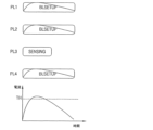
図2A~図2Cは、図1のメモリ装置100のピーク制御動作の多様な例を示す図である。
2A-2C are diagrams illustrating various examples of peak control operations of the
図2Aを参照すると、第1~第4メモリプレーン(PL1~PL4)の動作がいずれもピーク電力区間に該当する。例えば、第1~第4メモリプレーン(PL1~PL4)の動作がいずれもビットラインセットアップ区間BLSETUPに対応する。この時、第1~第4メモリプレーン(PL1~PL4)のそれぞれの動作に要求される電流量は、ビットラインセットアップ区間BLSETUPの初期にピーク値を有する。 Referring to FIG. 2A, operations of the first to fourth memory planes (PL1 to PL4) all correspond to the peak power period. For example, operations of the first to fourth memory planes (PL1 to PL4) all correspond to the bitline setup period BLSETUP. At this time, the amount of current required to operate each of the first to fourth memory planes PL1 to PL4 has a peak value at the beginning of the bitline setup period BLSETUP.
このように第1~第4メモリプレーン(PL1~PL4)のビットラインセットアップ区間BLSETUPが重畳する場合、第1~第4メモリプレーン(PL1~PL4)を含むメモリ装置100の全体電流量がピーク値を有し、この時、ピーク値は、臨界電流量THよりも高い。その結果、メモリ装置100で消耗される電力は、外部の電力管理モジュール、例えばPMICで提供可能な最大電流限界又は最大電力限界を超過してしまうため、メモリ装置100の正常動作を保証することが難しい。
When the bit line setup periods BLSETUP of the first to fourth memory planes PL1 to PL4 overlap, the total current of the
図2Bを参照すると、制御回路120は、第1~第4メモリプレーン(PL1~PL4)のビットラインセットアップ区間BLSETUPが重畳しないように、第1~第4メモリプレーン(PL1~PL4)の動作を時間的に分散させる。一実施例において、制御回路120は、第1~第4メモリプレーン(PL1~PL4)のビットラインセットアップ区間BLSETUPが全く重畳しないように、第1~第4メモリプレーン(PL1~PL4)の動作を時間的に完全に分散させる。これにより、メモリ装置100の全体電流量は臨界電流量THよりも十分に低く、メモリ装置100で消耗される電力はPMICで提供可能な最大電力限界よりも十分に低い。
Referring to FIG. 2B, the
例えば、第1メモリプレーンPL1のビットラインセットアップ区間BLSETUPの間、第1メモリプレーンPL1に対してビットラインセットアップ動作を正常に行わせ、第2~第4メモリプレーン(PL2~PL4)に対するビットラインセットアップ動作を中止させる。次いで、第1メモリプレーンPL1のビットラインセットアップ区間BLSETUPが終了すると、第2メモリプレーンPL2に対してビットラインセットアップ動作を再開(resume)させ、第3及び第4メモリプレーン(PL3、PL4)に対するビットラインセットアップ動作を継続して中止させる。次いで、第2メモリプレーンPL2のビットラインセットアップ区間BLSETUPが終了すると、第3メモリプレーンPL3に対してビットラインセットアップ動作を再開させ、第4メモリプレーンPL4に対するビットラインセットアップ動作を継続して中止させる。次いで、第3メモリプレーンPL3のビットラインセットアップ区間BLSETUPが終了すると、第4メモリプレーンPL4に対してビットラインセットアップ動作を再開させる。 For example, during the bitline setup period BLSETUP of the first memory plane PL1, the bitline setup operation is normally performed for the first memory plane PL1, and the bitline setup for the second to fourth memory planes PL2 to PL4 is performed. stop the action. Next, when the bitline setup period BLSETUP of the first memory plane PL1 ends, the bitline setup operation is resumed for the second memory plane PL2, and the bits for the third and fourth memory planes PL3 and PL4 are resumed. Continue to abort the line setup operation. After the bitline setup period BLSETUP of the second memory plane PL2 ends, the bitline setup operation for the third memory plane PL3 is resumed, and the bitline setup operation for the fourth memory plane PL4 is continuously stopped. After the bitline setup period BLSETUP of the third memory plane PL3 ends, the bitline setup operation of the fourth memory plane PL4 is resumed.
図2Cを参照すると、制御回路120は、第1~第4メモリプレーン(PL1~PL4)のビットラインセットアップ区間BLSETUPが完全に重畳しないように、第1~第4メモリプレーン(PL1~PL4)の動作を、時間的に部分的に分散させる。図2Aを参照して上述したように、第1~第4メモリプレーン(PL1~PL4)のそれぞれの動作に要求される電流量は、ビットラインセットアップ区間BLSETUPの初期にピーク値を有する。従って、制御回路120は、第1~第4メモリプレーン(PL1~PL4)のビットラインセットアップ区間BLSETUPの初期区間が重畳しないように、第1~第4メモリプレーン(PL1~PL4)の動作を時間的に分散させる。これにより、メモリ装置100の全体電流量は臨界電流量THよりも十分に低く、メモリ装置100で消耗される電力はPMICで提供可能な最大電力限界よりも十分に低い。
Referring to FIG. 2C, the
例えば、第1メモリプレーンPL1のビットラインセットアップ区間BLSETUPの間、第1メモリプレーンPL1に対してビットラインセットアップ動作を正常に行わせ、第1メモリプレーンPL1のビットラインセットアップ区間BLSETUPのうちの初期の一部区間の間、第2~第4メモリプレーン(PL2~PL4)に対するビットラインセットアップ動作を中止させる。次いで、第1メモリプレーンPL1のビットラインセットアップ区間BLSETUPのうちの初期の一部区間が終了すると、第2メモリプレーンPL2に対してビットラインセットアップ動作を再開させ、第3及び第4メモリプレーン(PL3、PL4)に対するビットラインセットアップ動作を継続して中止させる。次いで、第2メモリプレーンPL2のビットラインセットアップ区間BLSETUPの初期の一部区間が終了すると、第3メモリプレーンPL3に対してビットラインセットアップ動作を再開し、第4メモリプレーンPL4に対するビットラインセットアップ動作を継続して中止させる。次いで、第3メモリプレーンPL3のビットラインセットアップ区間BLSETUPの初期の一部区間が終了すると、第4メモリプレーンPL4に対してビットラインセットアップ動作を再開させる。 For example, during the bitline setup period BLSETUP of the first memory plane PL1, the bitline setup operation is normally performed on the first memory plane PL1, and the initial bitline setup period BLSETUP of the first memory plane PL1 is performed. The bitline setup operation for the second to fourth memory planes PL2 to PL4 is suspended during the partial period. Next, when the initial partial section of the bit line setup section BLSETUP of the first memory plane PL1 ends, the bit line setup operation is restarted for the second memory plane PL2, and the third and fourth memory planes PL3 , PL4) continue to abort the bit line setup operation. Next, when the initial partial section of the bitline setup section BLSETUP of the second memory plane PL2 ends, the bitline setup operation is resumed for the third memory plane PL3, and the bitline setup operation for the fourth memory plane PL4 is resumed. continue and stop. Then, when the initial partial period of the bitline setup period BLSETUP of the third memory plane PL3 ends, the bitline setup operation is resumed for the fourth memory plane PL4.
図3A~図3Cは、図1のメモリ装置100のピーク制御動作の更に多様な例を示す図である。
3A-3C are diagrams illustrating more various examples of peak control operations of the
図3Aを参照すると、第1~第4メモリプレーン(PL1~PL4)の動作のうちの一部の動作がピーク電力区間に対応する。例えば、第1、第2、及び第4メモリプレーン(PL1、PL2、PL4)の動作がビットラインセットアップ区間BLSETUPに対応し、第3メモリプレーンPL3の動作はセンシング区間SENSINGに対応する。ここで、センシング区間SENSINGは、読出動作のうちのプリチャージ区間、ディベロップ区間の後の区間に対応し、センシング区間SENSINGの電流又は電力消耗量は相対的に大きくない。ここで、第1、第2、及び第4メモリプレーン(PL1、PL2、PL4)のそれぞれの動作に要求される電流量は、ビットラインセットアップ区間BLSETUPの初期にピーク値を有する。 Referring to FIG. 3A, some of the operations of the first to fourth memory planes (PL1 to PL4) correspond to the peak power period. For example, operations of the first, second, and fourth memory planes PL1, PL2, and PL4 correspond to the bitline setup period BLSETUP, and operations of the third memory plane PL3 correspond to the sensing period SENSING. Here, the sensing period SENSING corresponds to the period after the precharge period and the develop period in the read operation, and current or power consumption in the sensing period SENSING is relatively small. Here, the amount of current required to operate each of the first, second, and fourth memory planes PL1, PL2, and PL4 has a peak value at the beginning of the bitline setup period BLSETUP.
このように第1、第2、及び第4メモリプレーン(PL1、PL2、PL4)のビットラインセットアップ区間BLSETUPが重畳する場合、第1~第4メモリプレーン(PL1~PL4)を含むメモリ装置100の全体電流量がピーク値を有し、この時、ピーク値は臨界電流量THよりも高い。その結果、メモリ装置100で消耗される電力は、外部の電力管理モジュール、例えばPMICで提供可能な最大電流限界又は最大電力限界を超過することがあり、メモリ装置100の正常動作を保証することが難しい。
When the bit line setup periods BLSETUP of the first, second, and fourth memory planes PL1, PL2, and PL4 overlap, the
図3Bを参照すると、制御回路120は、第1、第2、及び第4メモリプレーン(PL1、PL2、PL4)のビットラインセットアップ区間BLSETUPが重畳しないように、第1、第2、及び第4メモリプレーン(PL1、PL2、PL4)の動作を時間的に分散させる。制御回路120は、第1、第2、及び第4メモリプレーン(PL1、PL2、PL4)のビットラインセットアップ区間BLSETUPが全く重畳しないように、第1、第2、及び第4メモリプレーン(PL1、PL2、PL4)の動作を時間的に完全に分散させる。この時、制御回路120は、第3メモリプレーンPL3の動作を正常に行わせ、これにより、第1メモリプレーンPL1のビットラインセットアップ区間BLSETUPと第3メモリプレーンPL3のセンシング区間SENSINGとは重畳する。従って、メモリ装置100の全体電流量は臨界電流量THよりも十分に低く、メモリ装置100で消耗される電力はPMICで提供可能な最大電力限界よりも十分に低い。
Referring to FIG. 3B, the
例えば、第1メモリプレーンPL1のビットラインセットアップ区間BLSETUPの間、第1メモリプレーンPL1に対してビットラインセットアップ動作を正常に行わせ、第3メモリプレーンPL3に対してセンシング動作を正常に行わせ、第2及び第4メモリプレーン(PL2、PL4)に対するビットラインセットアップ動作を中止させる。次いで、第1メモリプレーンPL1のビットラインセットアップ区間BLSETUPが終了すると、第2メモリプレーンPL2に対してビットラインセットアップ動作を再開させ、第4メモリプレーンPL4に対するビットラインセットアップ動作を継続して中止させる。次いで、第2メモリプレーンPL2のビットラインセットアップ区間BLSETUPが終了すると、第4メモリプレーンPL4に対してビットラインセットアップ動作を再開させる。 For example, during the bitline setup period BLSETUP of the first memory plane PL1, the bitline setup operation is normally performed on the first memory plane PL1, the sensing operation is normally performed on the third memory plane PL3, Stop the bitline setup operation for the second and fourth memory planes (PL2, PL4). After the bitline setup period BLSETUP of the first memory plane PL1 ends, the bitline setup operation for the second memory plane PL2 is restarted, and the bitline setup operation for the fourth memory plane PL4 is continuously stopped. After the bitline setup period BLSETUP of the second memory plane PL2 ends, the bitline setup operation of the fourth memory plane PL4 is restarted.
図3Cを参照すると、制御回路120は、第1、第2、及び第4メモリプレーン(PL1、PL2、PL4)のビットラインセットアップ区間BLSETUPが完全に重畳しないように、第1、第2、及び第4メモリプレーン(PL1、PL2、PL4)の動作を、時間的に部分的に分散させる。図3Aを参照して上述したように、第1、第2、及び第4メモリプレーン(PL1、PL2、PL4)のそれぞれの動作に要求される電流量は、ビットラインセットアップ区間BLSETUPの初期にピーク値を有する。従って、制御回路120は、第1、第2、及び第4メモリプレーン(PL1、PL2、PL4)のビットラインセットアップ区間BLSETUPの初期区間が重畳しないように、第1、第2、及び第4メモリプレーン(PL1、PL2、PL4)の動作を時間的に分散させる。これにより、メモリ装置100の全体電流量は臨界電流量THよりも十分に低く、メモリ装置100で消耗される電力はPMICで提供可能な最大電力限界よりも十分に低い。
Referring to FIG. 3C, the
例えば、第1メモリプレーンPL1のビットラインセットアップ区間BLSETUPの間、第1メモリプレーンPL1に対してビットラインセットアップ動作を正常に行わせ、第3メモリプレーンPL3に対してセンシング動作を正常に行わせ、第2及び第4メモリプレーン(PL2、PL4)に対するビットラインセットアップ動作を中止させる。次いで、第1メモリプレーンPL1のビットラインセットアップ区間BLSETUPのうちの初期の一部区間が終了すると、第2メモリプレーンPL2に対してビットラインセットアップ動作を再開させ、第4メモリプレーンPL4に対するビットラインセットアップ動作を継続して中止させる。次いで、第2メモリプレーンPL2のビットラインセットアップ区間BLSETUPのうちの初期の一部区間が終了すると、第4メモリプレーンPL4に対してビットラインセットアップ動作を再開させる。 For example, during the bit line setup period BLSETUP of the first memory plane PL1, the bit line setup operation is normally performed on the first memory plane PL1, the sensing operation is normally performed on the third memory plane PL3, Stop the bitline setup operation for the second and fourth memory planes (PL2, PL4). Next, when the initial part of the bitline setup period BLSETUP of the first memory plane PL1 ends, the bitline setup operation of the second memory plane PL2 is resumed, and the bitline setup of the fourth memory plane PL4 is resumed. Continue and stop the action. Then, when the initial part of the bitline setup period BLSETUP of the second memory plane PL2 ends, the bitline setup operation of the fourth memory plane PL4 is restarted.
図4は、図1のメモリ装置100の構造を概略的に示す図である。
FIG. 4 is a schematic diagram of the structure of the
図4を参照すると、メモリ装置100は第1半導体層L1及び第2半導体層L2を含み、第1半導体層L1は第2半導体層L2上に第3方向に積層される。一実施例において、図1のメモリセルアレイ110は第1半導体層L1に形成され、図1の制御回路120は第2半導体層L2に形成される。これにより、メモリ装置100は、メモリセルアレイ110が制御回路120の上部に配置された構造、即ちCOP(Cell Over Periphery)構造を有する。例えば、メモリセルアレイ110を除いた周辺回路をメモリセルアレイ110下に配置することにより、COP構造は、積層方向に対して垂直な面に占める面積を効果的に減少させ、メモリ装置100の集積度を向上させる。
Referring to FIG. 4, the
第2半導体層L2は基板を含み、基板上にトランジスタのような半導体素子及び素子を配線するためのパターンを形成することで、第2半導体層L2に制御回路120を含む回路を形成する。第2半導体層L2に回路が形成された後、メモリセルアレイ110を含む第1半導体層L1が形成され、メモリセルアレイ110のワードラインWL及びビットラインBLと第2半導体層L2に形成された回路とを電気的に連結するためのパターンが形成される。
The second semiconductor layer L2 includes a substrate, and a circuit including the
図5は、図4の第2半導体層L2の上面を示す平面図である。 5 is a plan view showing the upper surface of the second semiconductor layer L2 of FIG. 4. FIG.
図1及び図5を共に参照すると、第2半導体層L2はパッド領域PAD及び周辺回路領域を含み、周辺回路領域は第1~第4領域(R1~R4)を含む。パッド領域PADには複数の入出力パッドPが配置され、複数の入出力パッドPは第2半導体層L2上のメタル配線を介して第1~第4領域(R1~R4)に連結される。第1領域R1の上部には第1メモリプレーンPL1が配置され、第2領域R2の上部には第2メモリプレーンPL2が配置され、第3領域R3の上部には第3メモリプレーンPL3が配置され、第4領域R4の上部には第4メモリプレーンPL4が配置される。 1 and 5, the second semiconductor layer L2 includes a pad area PAD and a peripheral circuit area, and the peripheral circuit area includes first to fourth areas (R1 to R4). A plurality of input/output pads P are arranged in the pad area PAD, and the plurality of input/output pads P are connected to the first to fourth areas (R1 to R4) through metal wiring on the second semiconductor layer L2. A first memory plane PL1 is arranged above the first region R1, a second memory plane PL2 is arranged above the second region R2, and a third memory plane PL3 is arranged above the third region R3. , a fourth memory plane PL4 is arranged above the fourth region R4.
第1領域R1には第1ロウデコーダRD1及び第1ページバッファPB1が配置され、第1ロウデコーダRD1及び第1ページバッファPB1は第1メモリプレーンPL1に連結される。第2領域R2には第2ロウデコーダRD2及び第2ページバッファPB2が配置され、第2ロウデコーダRD2及び第2ページバッファPB2は第2メモリプレーンPL2に連結される。第3領域R3には第3ロウデコーダRD3及び第3ページバッファPB3が配置され、第3ロウデコーダRD3及び第3ページバッファPB3は第3メモリプレーンPL3に連結される。第4領域R4には第4ロウデコーダRD4及び第4ページバッファPB4が配置され、第4ロウデコーダRD4及び第4ページバッファPB4は第4メモリプレーンPL4に連結される。図5では、第1~第4領域(R1~R4)のそれぞれに1つのロウデコーダ及び1つのページバッファが配置されるものとして図示したが、本発明は、これに限定されない。一実施例において、第1~第4領域(R1~R4)のそれぞれには、複数のロウデコーダ及び複数のページバッファが配置される。 A first row decoder RD1 and a first page buffer PB1 are arranged in the first region R1, and the first row decoder RD1 and the first page buffer PB1 are connected to the first memory plane PL1. A second row decoder RD2 and a second page buffer PB2 are arranged in the second region R2, and the second row decoder RD2 and the second page buffer PB2 are connected to the second memory plane PL2. A third row decoder RD3 and a third page buffer PB3 are arranged in the third region R3, and the third row decoder RD3 and the third page buffer PB3 are connected to the third memory plane PL3. A fourth row decoder RD4 and a fourth page buffer PB4 are arranged in the fourth region R4, and the fourth row decoder RD4 and the fourth page buffer PB4 are connected to the fourth memory plane PL4. Although one row decoder and one page buffer are arranged in each of the first to fourth regions (R1 to R4) in FIG. 5, the present invention is not limited to this. In one embodiment, a plurality of row decoders and a plurality of page buffers are arranged in each of the first to fourth regions (R1 to R4).
周辺回路領域の中心領域には、制御回路120が配置される。制御回路120は、第1~第4ロウデコーダ(RD1~RD4)に連結され、第1~第4ページバッファ(PB1~PB4)に連結される。これにより、制御回路120は、第1~第4メモリプレーン(PL1~PL4)の動作をモニタリングし、モニタリングの結果に基づいて第1~第4メモリプレーン(PL1~PL4)のピーク電力区間が少なくとも部分的に分散されるように、第1~第4メモリプレーン(PL1~PL4)の動作を制御する。図5では、制御回路120が周辺回路領域の中心領域に配置されるものとして図示したが、本発明は、これに限定されない。一実施例において、第1~第4領域(R1~R4)のうちの少なくとも1つに制御回路120が配置される。
A
図6は、図1の第1メモリプレーンPL1を示す図である。 FIG. 6 is a diagram showing the first memory plane PL1 of FIG.
図6を参照すると、第1メモリプレーンPL1は、複数のメモリブロック(BLK1~BLKi)を含む。複数のメモリブロック(BLK1~BLKi)のそれぞれは、3次元構造(又は垂直構造)を有する。具体的に、複数のメモリブロック(BLK1~BLKi)のそれぞれは、第1又は第2方向に沿って伸びた構造物を含む。例えば、各メモリブロックは、第3方向に沿って伸びた複数のNANDストリングを含む。この場合、複数のNANDストリングは、第1及び第2方向に沿って特定距離ほど離隔して提供される。 Referring to FIG. 6, the first memory plane PL1 includes a plurality of memory blocks (BLK1-BLKi). Each of the plurality of memory blocks (BLK1-BLKi) has a three-dimensional structure (or vertical structure). Specifically, each of the plurality of memory blocks (BLK1-BLKi) includes a structure extending along a first or second direction. For example, each memory block includes multiple NAND strings extending along the third direction. In this case, a plurality of NAND strings are provided separated by a certain distance along the first and second directions.
図5及び図6を共に参照すると、複数のメモリブロック(BLK1~BLKi)は、ロウデコーダRD1によって選択される。例えば、ロウデコーダRD1は、メモリブロック(BLK1~BLKi)のうちのブロックアドレスに対応するメモリブロックを選択する。図1の第2~第4メモリプレーン(PL2~PL4)も第1メモリプレーンPL1と実質的に同様に具現され、図6を参照して上述した内容は、第2~第4メモリプレーン(PL2~PL4)に対しても適用される。 5 and 6 together, a plurality of memory blocks (BLK1-BLKi) are selected by row decoder RD1. For example, the row decoder RD1 selects a memory block corresponding to a block address among memory blocks (BLK1 to BLKi). The second to fourth memory planes (PL2 to PL4) of FIG. 1 are implemented substantially in the same manner as the first memory plane PL1, and the contents described above with reference to FIG. ~PL4).
図7Aは、図6の第1メモリブロックBLK1の等価回路図である。 FIG. 7A is an equivalent circuit diagram of the first memory block BLK1 of FIG.
図7Aを参照すると、第1メモリブロックBLK1は、複数のNANDストリング(NS11~NS33)、複数のワードライン(WL1~WL8)、複数のビットライン(BL1~BL3)、複数の接地選択ライン(GSL1~GSL3)、複数のストリング選択ライン(SSL1~SSL3)、及び共通ソースラインCSLを含む。ここで、NANDストリングの個数、ワードラインの個数、ビットラインの個数、接地選択ラインの個数、及びストリング選択ラインの個数は、実施例によって多様に変更される。 Referring to FIG. 7A, the first memory block BLK1 includes a plurality of NAND strings (NS11˜NS33), a plurality of wordlines (WL1˜WL8), a plurality of bitlines (BL1˜BL3), and a plurality of ground selection lines (GSL1). GSL3), a plurality of string select lines (SSL1-SSL3), and a common source line CSL. Here, the number of NAND strings, the number of wordlines, the number of bitlines, the number of ground selection lines, and the number of string selection lines may vary according to embodiments.
第1ビットラインBL1と共通ソースラインCSLとの間にNANDストリング(NS11、NS21、NS31)が提供され、第2ビットラインBL2と共通ソースラインCSLとの間にNANDストリング(NS12、NS22、NS32)が提供され、第3ビットラインBL3と共通ソースラインCSLとの間にNANDストリング(NS13、NS23、NS33)が提供される。各NANDストリング(例えば、NS11)は、直列連結されたストリング選択トランジスタSST、複数のメモリセルMC、及び接地選択トランジスタGSTを含む。 NAND strings NS11, NS21 and NS31 are provided between the first bitline BL1 and the common source line CSL, and NAND strings NS12, NS22 and NS32 are provided between the second bitline BL2 and the common source line CSL. is provided, and a NAND string (NS13, NS23, NS33) is provided between the third bit line BL3 and the common source line CSL. Each NAND string (eg, NS11) includes a serially connected string select transistor SST, a plurality of memory cells MC, and a ground select transistor GST.
ストリング選択トランジスタSSTは、対応するストリング選択ライン(SSL1~SSL3)に連結される。複数のメモリセルMCは、それぞれ対応するワードライン(WL1~WL8)に連結される。接地選択トランジスタGSTは、対応する接地選択ライン(GSL1~GSL3)に連結される。ストリング選択トランジスタSSTは対応するビットライン(BL1~BL3)に連結され、接地選択トランジスタGSTは共通ソースラインCSLに連結される。 The string select transistors SST are connected to corresponding string select lines SSL1 to SSL3. A plurality of memory cells MC are connected to corresponding word lines WL1 to WL8. The ground select transistors GST are connected to corresponding ground select lines GSL1-GSL3. The string select transistors SST are connected to corresponding bitlines BL1 to BL3, and the ground select transistors GST are connected to a common source line CSL.
本実施例において、同じ高さのワードライン(例えば、WL1)はそれぞれ共通連結され、ストリング選択ライン(SSL1~SSL3)はそれぞれ分離されて、接地選択ライン(GSL1~GSL3)もそれぞれ分離される。図7では、3本のストリング選択ライン(SSL1~SSL3)が同じ高さのワードラインを共有するものとして図示したが、本発明は、これに限定されない。例えば、2本のストリング選択ラインが同じ高さのワードラインを共有する。他の例として、4本のストリング選択ラインが同じ高さのワードラインを共有する。 In this embodiment, the same-height word lines (eg, WL1) are connected together, the string selection lines (SSL1-SSL3) are isolated from each other, and the ground selection lines (GSL1-GSL3) are isolated from each other. Although FIG. 7 illustrates three string select lines (SSL1-SSL3) as sharing the same height word line, the present invention is not so limited. For example, two string select lines share the same height word line. As another example, four string select lines share the same height word line.
図7Bは、図6の第1メモリブロックBLK1を示す斜視図である。 7B is a perspective view showing the first memory block BLK1 of FIG. 6. FIG.
図7Bを参照すると、第1メモリブロックBLK1は、基板SUBに対して垂直方向に形成される。基板SUBは、第1導電型(例えば、pタイプ)を有し、基板SUB上に第1方向に沿って伸び、第2導電型(例えば、nタイプ)の不純物がドーピングされた共通ソースラインCSLが提供される。隣接する2本の共通ソースラインCSL間の基板SUB領域上に、第1方向に沿って伸びる複数の絶縁膜ILが第3方向に沿って順次に提供され、複数の絶縁膜ILが第3方向に沿って特定距離ほど離隔される。例えば、複数の絶縁膜ILは、シリコン酸化物のような絶縁物質を含む。 Referring to FIG. 7B, the first memory block BLK1 is formed vertically with respect to the substrate SUB. The substrate SUB has a first conductivity type (eg, p-type), extends along the first direction above the substrate SUB, and is doped with a second conductivity type (eg, n-type) common source line CSL. is provided. A plurality of insulating films IL extending along the first direction are sequentially provided along the third direction over the substrate SUB region between two adjacent common source lines CSL. are separated by a specified distance along the . For example, the plurality of insulating films IL includes an insulating material such as silicon oxide.
隣接する2本の共通ソースラインCSL間の基板SUB領域上に、第1方向に沿って順次に配置され、第3方向に沿って複数の絶縁膜ILを貫通する複数のピラー(pillars)Pが提供される。例えば、複数のピラーPは、複数の絶縁膜ILを貫通して基板SUBにコンタクトする。具体的に、各ピラーPの表面層(surface layer)Sは、第1タイプを有するシリコン物質を含み、チャネル領域として機能する。一方、各ピラーPの内部層Iは、シリコン酸化物のような絶縁物質又はエアギャップ(air gap)を含む。 A plurality of pillars P are sequentially arranged along the first direction and penetrate the plurality of insulating films IL along the third direction on the substrate SUB region between two adjacent common source lines CSL. provided. For example, the multiple pillars P penetrate the multiple insulating films IL and contact the substrate SUB. Specifically, a surface layer S of each pillar P includes a silicon material having a first type and functions as a channel region. Meanwhile, the inner layer I of each pillar P includes an insulating material such as silicon oxide or an air gap.
隣接する2本の共通ソースラインCSL間の領域で、絶縁膜IL、ピラーP、及び基板SUBの露出した表面に沿って電荷保存層(charge storage layer)CSが提供される。電荷保存層CSは、ゲート絶縁層(又は「トンネリング絶縁層」と称する)、電荷トラップ層、及びブロッキング絶縁層を含む。例えば、電荷保存層CSは、ONO(oxide-nitride-oxide)構造を有する。また、隣接する2本の共通ソースラインCSL間の領域で、電荷保存層CSの露出した表面上に、選択ライン(GSL、SSL)及びワードライン(WL1~WL8)のようなゲート電極GEが提供される。 A charge storage layer CS is provided along exposed surfaces of the insulating layer IL, the pillar P, and the substrate SUB in the region between two adjacent common source lines CSL. The charge storage layer CS includes a gate insulating layer (also called a "tunneling insulating layer"), a charge trapping layer, and a blocking insulating layer. For example, the charge storage layer CS has an ONO (oxide-nitride-oxide) structure. Also, gate electrodes GE such as select lines (GSL, SSL) and word lines (WL1-WL8) are provided on the exposed surface of the charge storage layer CS in the region between two adjacent common source lines CSL. be done.
複数のピラーP上には、ドレイン又はドレインコンタクトDRがそれぞれ提供される。例えば、ドレイン又はドレインコンタクトDRは、第2導電型を有する不純物がドーピングされたシリコン物質を含む。ドレインDR上に、第2方向に伸びて第1方向に沿って特定距離ほど離隔して配置されたビットライン(BL1~BL3)が提供される。 A drain or drain contact DR is provided on the plurality of pillars P, respectively. For example, the drain or drain contact DR includes silicon material doped with impurities having the second conductivity type. Bit lines BL1 to BL3 are provided on the drains DR and extend in the second direction and are spaced apart from each other by a specific distance along the first direction.
図8は、図5のメモリ装置100を示す断面図である。
FIG. 8 is a cross-sectional view of the
図8を参照すると、第2半導体層L2は、基板SUB、第2下部絶縁層IL22、及び第1下部絶縁層IL21を含み、第2半導体層L2には、図1の制御回路120が配置される。基板SUBは、単結晶シリコン又は単結晶ゲルマニウムのような半導体物質を含む半導体基板であり、シリコンウェーハから製造される。第1及び第2下部絶縁層(IL21、IL22)は、シリコン酸化物のような絶縁物質を用いて化学気相蒸着(chemical vapor deposition:CVD)工程、スピンコーティング工程などを通じて形成される。
Referring to FIG. 8, the second semiconductor layer L2 includes a substrate SUB, a second lower insulating layer IL22, and a first lower insulating layer IL21, and the
第2半導体層L2に含まれる基板SUB上に複数の半導体素子、例えばトランジスタTRが形成され、半導体素子は第2下部絶縁層IL22を貫通するコンタクトプラグCP21を介して第1下部絶縁層IL21に形成されたメタルパターンMP21に電気的に連結される。第2半導体層L2に形成された半導体素子は、図5の第1~第4ロウデコーダ(RD1~RD4)、第1~第4ページバッファ(PB1~PB4)、及び制御回路120に対応する回路を構成する。
A plurality of semiconductor elements such as transistors TR are formed on the substrate SUB included in the second semiconductor layer L2, and the semiconductor elements are formed in the first lower insulating layer IL21 via contact plugs CP21 penetrating the second lower insulating layer IL22. is electrically connected to the metal pattern MP21. The semiconductor elements formed in the second semiconductor layer L2 are circuits corresponding to the first to fourth row decoders (RD1 to RD4), the first to fourth page buffers (PB1 to PB4), and the
第1半導体層L1は第2半導体層L2上に積層され、第1半導体層L1には図1のメモリセルアレイ110が配置される。第1半導体層L1は、ベース層BP及び上部絶縁層IL10を含む。一実施例において、ベース層BPは、ポリシリコンを使用してスパッタリング工程、CVD工程、原子層蒸着(atomic layer deposition:ALD)工程、物理気相蒸着(physical vapor deposition:PVD)工程などを通じて形成される。一実施例において、ベース層BPは、第1下部絶縁層IL21上に非晶質シリコン層を形成した後、熱処理又はレーザビームの照射によって非晶質シリコン層を単結晶シリコン層に変化させて形成され、これによって、ベース層BP内の欠陥が除去される。一実施例において、ベース層BPは、ウェーハボンディング(wafer bonding)工程を介して形成され、この場合、第1下部絶縁層IL21上に、例えば単結晶シリコンウェーハを付着させ、ウェーハの上部を部分的に除去するか平坦化することで、ベース層BPが形成される。
The first semiconductor layer L1 is laminated on the second semiconductor layer L2, and the
また、図7Bを参照して上述したように、第1半導体層L1でストリング選択ラインSSL、ワードライン(WL1~WL8)、及び接地選択ラインGSLがベース層BP上に第3方向に積層され、積層されたストリング選択ラインSSL、ワードライン(WL1~WL8)、及び接地選択ラインGSLを貫通するピラーPが形成される。 Further, as described above with reference to FIG. 7B, the string selection lines SSL, the word lines (WL1 to WL8), and the ground selection lines GSL are stacked on the base layer BP in the third direction in the first semiconductor layer L1, Pillars P are formed through the stacked string select lines SSL, word lines WL1-WL8, and ground select lines GSL.
図9は、本発明の他の実施形態によるメモリシステム10aを概略的に示すブロック図である。
FIG. 9 is a block diagram that schematically illustrates a
図9を参照すると、メモリシステム10aは、図1のメモリシステム10の変形実施例に対応し、図1~図8を参照して上述した内容は、本実施例にも適用される。メモリシステム10aは、メモリ装置100a及びメモリコントローラ200を含む。メモリ装置100aは、不揮発性メモリ装置であり、メモリチップとして具現される。メモリ装置100aはメモリセルアレイ110及び制御回路120aを含み、メモリセルアレイ110及び制御回路120aは単一メモリチップとして具現される。本実施例による制御回路120aは、図1の制御回路120と異なって具現されるため、以下では、制御回路120aを中心に説明する。
Referring to FIG. 9,
制御回路120aは、第1~第4制御ロジック(control logics)(CL1~CL4)を含む。第1~第4制御ロジック(CL1~CL4)は、それぞれ第1~第4メモリプレーン(PL1~PL4)に対応し、それぞれ第1~第4メモリプレーン(PL1~PL4)の動作を制御する。以下、図10を参照して第1~第4制御ロジック(CL1~CL4)の具体的な動作について詳述する。
The
図10は、図9のメモリ装置100aを示すブロック図である。
FIG. 10 is a block diagram illustrating the
図9及び図10を共に参照すると、メモリ装置100aは、第1~第4メモリプレーン(PL1~PL4)を含むメモリセルアレイ110を含み、例えばメモリセルアレイ110は、図4の第1半導体層L1に配置される。また、メモリ装置100aは、第1~第4ロウデコーダ(RD1~RD4)、第1~第4ページバッファ(PB1~PB4)、及び第1~第4制御ロジック(CL1~CL4)を更に含み、例えば第1~第4ロウデコーダ(RD1~RD4)、第1~第4ページバッファ(PB1~PB4)、及び第1~第4制御ロジック(CL1~CL4)は、図4の第2半導体層L2に配置される。
Referring to both FIGS. 9 and 10, the
第1制御ロジックCL1は、第1メモリプレーンPL1の動作をモニタリングすることで第1モニタリング信号MS1を生成し、生成された第1モニタリング信号MS1を第2~第4制御ロジック(CL2~CL4)に提供する。一実施例において、第1メモリプレーンPL1がピーク電力区間に進入した場合、第1モニタリング信号MS1は活性化され、例えばロジックハイレベルを有する。一実施例において、第1メモリプレーンPL1がピーク電力区間に進入していない場合、第1モニタリング信号MS1は、非活性化され、例えばロジックロウレベルを有する。例えば、第1モニタリング信号MS1は、フラグとして具現される。 The first control logic CL1 monitors the operation of the first memory plane PL1 to generate the first monitoring signal MS1, and sends the generated first monitoring signal MS1 to the second to fourth control logics CL2 to CL4. offer. In one embodiment, when the first memory plane PL1 enters a peak power period, the first monitoring signal MS1 is activated, eg, having a logic high level. In one embodiment, when the first memory plane PL1 has not entered the peak power period, the first monitoring signal MS1 is inactivated, eg, having a logic low level. For example, the first monitoring signal MS1 is embodied as a flag.
同様に、第2制御ロジックCL2は、第2メモリプレーンPL2の動作をモニタリングすることで第2モニタリング信号MS2を生成し、生成された第2モニタリング信号MS2を第1、第3及び第4制御ロジック(CL1、CL3、CL4)に提供する。第3制御ロジックCL3は、第3メモリプレーンPL3の動作をモニタリングすることで第3モニタリング信号MS3を生成し、生成された第3モニタリング信号MS3を第1、第2及び第4制御ロジック(CL1、CL2、CL4)に提供する。第4制御ロジックCL4は、第4メモリプレーンPL4の動作をモニタリングすることで第4モニタリング信号MS4を生成し、生成された第4モニタリング信号MS4を第1~第3制御ロジック(CL1~CL3)に提供する。 Similarly, the second control logic CL2 monitors the operation of the second memory plane PL2 to generate a second monitoring signal MS2, and distributes the generated second monitoring signal MS2 to the first, third and fourth control logics. (CL1, CL3, CL4). The third control logic CL3 monitors the operation of the third memory plane PL3 to generate a third monitoring signal MS3, and the generated third monitoring signal MS3 is applied to the first, second and fourth control logic CL1, CL1, and CL1. CL2, CL4). The fourth control logic CL4 monitors the operation of the fourth memory plane PL4 to generate a fourth monitoring signal MS4, and sends the generated fourth monitoring signal MS4 to the first to third control logics CL1 to CL3. offer.
第1制御ロジックCL1は、第1モニタリング信号MS1に基づいて第1メモリプレーンPL1がピーク電力区間に進入したか否かを判断する。判断の結果、第1メモリプレーンPL1がピーク電力区間に進入した場合、第1制御ロジックCL1は、第2~第4モニタリング信号(MS2~MS4)に基づいて第2~第4メモリプレーン(PL2~PL4)がピーク電力区間に進入したか否かを判断する。 The first control logic CL1 determines whether the first memory plane PL1 enters the peak power period based on the first monitoring signal MS1. As a result of the determination, if the first memory plane PL1 has entered the peak power period, the first control logic CL1 controls the second to fourth memory planes PL2 to PL based on the second to fourth monitoring signals MS2 to MS4. PL4) determines whether the peak power interval has been entered.
判断の結果、第2~第4メモリプレーン(PL2~PL4)のうちの少なくとも1つがピーク電力区間に進入した場合、第1制御ロジックCL1は、第1メモリプレーンPL1の動作を遅延又は中止させる。一実施例において、第1制御ロジックCL1は、活性化された第2~第4モニタリング信号(MS2~MS4)のうちの少なくとも1つが非活性化されると、第2~第4メモリプレーン(PL2~PL4)のうちの少なくとも1つがピーク電力区間から外れたと判断し、第1メモリプレーンPL1の動作を再開させる。一実施例において、第1制御ロジックCL1は、第1メモリプレーンPL1の動作の中止時点から既定の時間が経過すると、第1メモリプレーンPL1の動作を再開させる。 As a result of the determination, if at least one of the second to fourth memory planes PL2 to PL4 enters the peak power period, the first control logic CL1 delays or suspends the operation of the first memory plane PL1. In one embodiment, the first control logic CL1 controls the second to fourth memory planes (PL2) when at least one of the activated second to fourth monitoring signals (MS2 to MS4) is deactivated. to PL4) is out of the peak power interval, and the operation of the first memory plane PL1 is resumed. In one embodiment, the first control logic CL1 resumes the operation of the first memory plane PL1 after a predetermined time has passed since the operation of the first memory plane PL1 was stopped.
図11は、図4の第2半導体層L2aの一例の上面を示す平面図である。 FIG. 11 is a plan view showing an example top surface of the second semiconductor layer L2a of FIG.
図4、図9、図10、及び図11を共に参照すると、第2半導体層L2aはパッド領域PAD及び周辺回路領域を含み、周辺回路領域は第1~第4領域(R1~R4)を含む。パッド領域PADには複数の入出力パッドPが配置され、複数の入出力パッドPは第2半導体層L2上のメタル配線を介して第1~第4領域(R1~R)4に連結される。第1領域R1の上部には第1メモリプレーンPL1が配置され、第2領域R2の上部には第2メモリプレーンPL2が配置され、第3領域R3の上部には第3メモリプレーンPL3が配置され、第4領域R4の上部には第4メモリプレーンPL4が配置される。 4, 9, 10, and 11, the second semiconductor layer L2a includes a pad area PAD and a peripheral circuit area, and the peripheral circuit area includes first to fourth areas (R1 to R4). . A plurality of input/output pads P are arranged in the pad area PAD, and the plurality of input/output pads P are connected to the first to fourth areas (R1 to R) 4 via metal wiring on the second semiconductor layer L2. . A first memory plane PL1 is arranged above the first region R1, a second memory plane PL2 is arranged above the second region R2, and a third memory plane PL3 is arranged above the third region R3. , a fourth memory plane PL4 is arranged above the fourth region R4.
第1領域R1には、第1ロウデコーダRD1、第1ページバッファPB1、及び第1制御ロジックCL1が配置される。第2領域R2には、第2ロウデコーダRD2、第2ページバッファPB2、及び第2制御ロジックCL2が配置される。第3領域R3には、第3ロウデコーダRD3、第3ページバッファPB3、及び第3制御ロジックCL3が配置される。第4領域R4には、第4ロウデコーダRD4、第4ページバッファPB4、及び第4制御ロジックCL4が配置される。図11では、第1~第4領域(R1~R4)のそれぞれに1つのロウデコーダ及び1つのページバッファが配置されるものとして図示したが、本発明は、これに限定されない。一実施例において、第1~第4領域(R1~R4)のそれぞれには、複数のロウデコーダ及び複数のページバッファが配置される。また、実施例によって、第1~第4領域(R1~R4)のそれぞれでロウデコーダ、ページバッファ、及び制御ロジックの配置は、多様に変更される。 A first row decoder RD1, a first page buffer PB1, and a first control logic CL1 are arranged in the first region R1. A second row decoder RD2, a second page buffer PB2, and a second control logic CL2 are arranged in the second region R2. A third row decoder RD3, a third page buffer PB3, and a third control logic CL3 are arranged in the third region R3. A fourth row decoder RD4, a fourth page buffer PB4, and a fourth control logic CL4 are arranged in the fourth region R4. Although one row decoder and one page buffer are arranged in each of the first to fourth regions (R1 to R4) in FIG. 11, the present invention is not limited to this. In one embodiment, a plurality of row decoders and a plurality of page buffers are arranged in each of the first to fourth regions (R1 to R4). In addition, the arrangement of row decoders, page buffers, and control logic in each of the first to fourth regions (R1 to R4) may vary according to embodiments.
第1制御ロジックCL1は、第2~第4制御ロジック(CL2~CL4)に連結され、第2~第4制御ロジック(CL2~CL4)から第2~第4モニタリング信号(MS2~MS4)を受信し、第2~第4制御ロジック(CL2~CL4)に第1モニタリング信号MS1を提供する。第1制御ロジックCL1は、第1ロウデコーダRD1及び第1ページバッファPB1に連結される。これにより、第1制御ロジックCL1は、第1~第4メモリプレーン(PL1~PL4)の動作をモニタリングし、モニタリングの結果に基づいて第1~第4メモリプレーン(PL1~PL4)のピーク電力区間が少なくとも部分的に分散されるように、第1メモリプレーンPL1の動作を制御する。 The first control logic CL1 is connected to the second to fourth control logics (CL2 to CL4) and receives the second to fourth monitoring signals (MS2 to MS4) from the second to fourth control logics (CL2 to CL4). and provides a first monitoring signal MS1 to the second to fourth control logics (CL2 to CL4). The first control logic CL1 is connected to the first row decoder RD1 and the first page buffer PB1. Accordingly, the first control logic CL1 monitors the operation of the first to fourth memory planes (PL1 to PL4), and based on the monitoring result, the peak power period of the first to fourth memory planes (PL1 to PL4). is at least partially distributed.
図12A及び図12Bは、図9のメモリ装置100aのピーク制御動作の多様な例を示す図である。
12A and 12B illustrate various examples of peak control operations of the
第1制御ロジックCL1は、第1~第4モニタリング信号(MS1~MS4)に基づいて第1~第4メモリプレーン(PL1~PL4)の動作がいずれもピーク電力区間に対応すると判断した場合、例えば第1~第4メモリプレーン(PL1~PL4)の動作がいずれもビットラインセットアップ区間BLSETUPに対応する場合、第1制御ロジックCL1は、第1~第4メモリプレーン(PL1~PL4)のビットラインセットアップ区間BLSETUPが重畳しないように、第1メモリプレーンPL1のビットラインセットアップ動作を中止させる。 When the first control logic CL1 determines that the operations of the first to fourth memory planes (PL1 to PL4) all correspond to the peak power period based on the first to fourth monitoring signals (MS1 to MS4), for example When the operations of the first to fourth memory planes PL1 to PL4 all correspond to the bitline setup period BLSETUP, the first control logic CL1 performs bitline setup of the first to fourth memory planes PL1 to PL4. The bitline setup operation of the first memory plane PL1 is stopped so that the interval BLSETUP does not overlap.
例えば、図12Aを参照すると、第1制御ロジックCL1は、第2~第4メモリプレーン(PL2~PL4)のビットラインセットアップ区間BLSETUPが終了するまで、第1メモリプレーンPL1に対してビットラインセットアップ動作を中止させる。第1制御ロジックCL1は、PMICの最大電力限界を考慮して、第1メモリプレーンPL1に対するビットラインセットアップ動作の再開時点を適応的に決定する。第1制御ロジックCL1は、第2~第4メモリプレーン(PL2~PL4)のビットラインセットアップ区間BLSETUPがいずれも終了すると、第1メモリプレーンPL1に対するビットラインセットアップ動作を再開させる。一実施例において、第1制御ロジックCL1は、第2~第4メモリプレーン(PL2~PL4)のうちの少なくとも1つのビットラインセットアップ区間BLSETUPが終了すると、第1メモリプレーンPL1に対するビットラインセットアップ動作を再開させる。 For example, referring to FIG. 12A, the first control logic CL1 performs a bitline setup operation on the first memory plane PL1 until the bitline setup period BLSETUP of the second to fourth memory planes PL2 to PL4 ends. discontinue. The first control logic CL1 adaptively determines when to restart the bitline setup operation for the first memory plane PL1, taking into account the maximum power limit of the PMIC. The first control logic CL1 restarts the bitline setup operation for the first memory plane PL1 when the bitline setup periods BLSETUP of the second to fourth memory planes PL2 to PL4 are completed. In one embodiment, the first control logic CL1 performs a bitline setup operation on the first memory plane PL1 after a bitline setup period BLSETUP of at least one of the second to fourth memory planes PL2 to PL4. let it resume.
図12Bを参照すると、第1制御ロジックCL1は、第1~第4メモリプレーン(PL1~PL4)のビットラインセットアップ区間BLSETUPが完全に重畳しないように、第1メモリプレーンPL1のビットラインセットアップ動作を中止させる。図2Aを参照して上述したように、第1~第4メモリプレーン(PL1~PL4)のそれぞれの動作に要求される電流量は、ビットラインセットアップ区間BLSETUPの初期にピーク値を有する。従って、第1制御ロジックCL1は、第1~第4メモリプレーン(PL1~PL4)のビットラインセットアップ区間BLSETUPの初期区間が重畳しないように、第1メモリプレーンPL1のビットラインセットアップ動作を中止させる。例えば、第1制御ロジックCL1は、予め決められた一定時間区間、第1メモリプレーンPL1に対するビットラインセットアップ動作を中止させる。 Referring to FIG. 12B, the first control logic CL1 controls the bitline setup operation of the first memory plane PL1 so that the bitline setup periods BLSETUP of the first to fourth memory planes PL1 to PL4 do not completely overlap. discontinue. As described above with reference to FIG. 2A, the amount of current required to operate each of the first to fourth memory planes PL1 to PL4 has a peak value at the beginning of the bitline setup period BLSETUP. Accordingly, the first control logic CL1 suspends the bitline setup operation of the first memory plane PL1 so that the initial periods of the bitline setup periods BLSETUP of the first to fourth memory planes PL1 to PL4 do not overlap. For example, the first control logic CL1 suspends the bitline setup operation for the first memory plane PL1 for a predetermined period of time.
図13は、本発明の一実施形態によるメモリ装置の動作方法を示すフローチャートである。 FIG. 13 is a flowchart illustrating a method of operating a memory device according to an embodiment of the inventive concept.
図13を参照すると、メモリ装置の動作は、単一メモリチップに含まれる複数のメモリプレーンのピーク電力又はピーク電流を制御する動作に対応し、例えば図1のメモリ装置100又は図9のメモリ装置100aで行われる。図1~図12Bを参照して上述した内容は本実施例にも適用され、重複説明は省略する。
Referring to FIG. 13, the operation of a memory device corresponds to controlling the peak power or peak current of multiple memory planes included in a single memory chip, such as
段階S110において、複数のメモリプレーンの動作をモニタリングする。一実施例において、制御回路120のモニタリングロジック121は、複数のメモリプレーンの動作をモニタリングすることでモニタリング信号MSを生成する。一実施例において、第1~第4制御ロジック(CL1~CL4)のそれぞれは対応するメモリプレーンの動作をモニタリングすることで第1~第4モニタリング信号(MS1~MS4)をそれぞれ生成する。
In step S110, the operation of multiple memory planes is monitored. In one embodiment,
段階S120において、少なくとも1つのメモリプレーンがピーク電力区間に対応するか否かを判断する。一実施例において、制御回路120のモニタリングロジック121は、複数のメモリプレーンのうちの少なくとも1つがピーク電力区間に進入したか否かを判断する。判断の結果、少なくとも1つのメモリプレーンがピーク電力区間に対応する場合、段階S130を行い、そうではない場合、段階S150を行う。
At step S120, it is determined whether at least one memory plane corresponds to the peak power interval. In one embodiment,
段階S130において、他のメモリプレーンがピーク電力区間に対応するか否かを判断する。一実施例において、制御回路120のモニタリングロジック121は、複数のメモリプレーンのうちの少なくとも1つの他のメモリプレーンがピーク電力区間に進入したか否かを判断する。判断の結果、他のメモリプレーンがピーク電力区間に対応する場合、段階S140を行い、そうではない場合、段階S150を行う。
At step S130, it is determined whether another memory plane corresponds to the peak power interval. In one embodiment,
一実施例において、メモリ装置の動作方法は、段階S120とS130との間に、複数のプレーン間の優先順位情報を用いて他のメモリプレーンを決定する段階を更に含む。具体的に、モニタリングロジック121は、段階S120でピーク電力区間に対応すると判断されたメモリプレーンよりも高い優先順位を有するメモリプレーンがピーク電力区間に対応するか否かを判断する。
In one embodiment, the method of operating the memory device further includes, between steps S120 and S130, determining another memory plane using priority information among the plurality of planes. Specifically, the
段階S140において、ピーク電力区間が少なくとも部分的に分散されるように複数のメモリプレーンの動作を制御する。一実施例において、制御回路120のピーク制御ロジック122は、ピーク電力区間が完全に重畳しないように、一部のメモリプレーンの動作を中止させる。一実施例において、制御回路120のピーク制御ロジック122は、ピーク電力区間の初期区間が重畳されないように、一部メモリプレーンの動作を中止させる。段階S150において、少なくとも1つのメモリプレーンに対する動作を進める。一実施例において、制御回路120のピーク制御ロジック122は、少なくとも1つのメモリプレーンに対する動作が正常に行われるように、ロウデコーダ及びページバッファなどを制御する。
At step S140, the operation of the plurality of memory planes is controlled such that the peak power intervals are at least partially distributed. In one embodiment, the peak control logic 122 of the
図14は、本発明の一実施形態によるメモリコントローラ200とメモリ装置100との間の動作を示すフローチャートである。
FIG. 14 is a flowchart illustrating operations between the
図14を参照すると、本実施形態は、図13の動作方法の一具現例に対応し、図1~図13を参照して上述した内容は本実施例にも適用され、重複説明は省略する。図14では、メモリ装置が図1のメモリ装置100に対応するものとして図示したが、本発明はこれに限定されず、図14のメモリ装置は図9のメモリ装置100aに対応してもよい。
Referring to FIG. 14, this embodiment corresponds to an embodiment of the operation method of FIG. 13, and the contents described above with reference to FIGS. . Although FIG. 14 illustrates the memory device as corresponding to the
段階S210において、メモリコントローラ200は、ピーク電力区間を指定する。例えば、メモリコントローラ200のピーク区間決定部210は、ピーク電力区間、ピーク電流区間、又はピーク制御区間を指定する。例えば、ピーク電力区間は、プログラム動作のためのビットラインセットアップ区間、読出動作のためのビットラインプリチャージ区間、及びプログラム動作又は読出動作前のラッチ初期化区間のうちの少なくとも1つに該当する。
At step S210, the
S220において、メモリコントローラ200は、複数のプレーン間の優先順位を指定する。例えば、メモリコントローラ200のプレーン優先順位決定部220は、複数のプレーン間の優先順位を決定する。一実施例において、段階S210と段階S220は、実質的に同時に行われる。他の実施例において、段階S220が先に行われ、次いで段階S210が行われる。
In S220, the
一実施例において、ピーク電力区間に関する情報及びプレーン優先順位情報は、メモリ装置100の出荷時に予め決定され、メモリ装置100のメモリセルアレイ110にプログラムされる。メモリシステム10に電源が印加されると、即ちブーティングの後、メモリコントローラ200は、IDRを通じてメモリセルアレイ110にプログラムされたピーク電力区間に関する情報及びプレーン優先順位情報を読出す。
In one embodiment, the peak power interval information and plane priority information are predetermined and programmed into the
段階S230において、メモリコントローラ200は、メモリ装置100にアドレスADDR、コマンドCMD、及び制御信号CTRLを伝送する。一実施例において、メモリコントローラ200は、プログラム動作を行うように、メモリ装置100にデータを更に伝送する。一実施例において、メモリコントローラ200は、ピーク電力区間に関する情報及び優先順位情報を、セットフィーチャーコマンドを用いてメモリ装置100に伝送する。
At step S230, the
段階S240において、メモリ装置100は、第1メモリプレーンPL1の動作をモニタリングする。例えば、図1のモニタリングロジック121又は図9の第1制御ロジックCL1は、第1メモリプレーンPL1の動作がピーク電力区間に対応するか否かを判断することで、モニタリング信号を生成する。段階S250において、メモリ装置100は、第1メモリプレーンPL1がピーク電力区間に対応するか否かを判断する。判断の結果、第1メモリプレーンPL1がピーク電力区間に対応する場合、段階S270を行い、そうではない場合、段階S290を行う。
In operation S240, the
段階S260において、メモリ装置100は、第2メモリプレーンPL2の動作をモニタリングする。例えば、図1のモニタリングロジック121又は図9の第2制御ロジックCL2は、第2メモリプレーンPL2の動作がピーク電力区間に対応するか否かを判断することで、モニタリング信号を生成する。段階S270において、メモリ装置100は、第2メモリプレーンPL2がピーク電力区間に対応するか否かを判断する。判断の結果、第2メモリプレーンPL2がピーク電力区間に対応する場合、段階S280を行い、そうではない場合、段階S290を行う。
In operation S260, the
段階S280において、メモリ装置100は、第1メモリプレーンPL1の動作を中止する。例えば、図1のピーク制御ロジック122又は図9の第1制御ロジックCL1は、第1メモリプレーンPL1の動作を一定時間中止させる。段階S290において、メモリ装置100は、第1メモリプレーンPL1の動作を進める。例えば、図1のピーク制御ロジック122又は図9の第1制御ロジックCL1は、第1メモリプレーンPL1の動作を進める。また、段階S280の後、一定時間が経過すると、図1のピーク制御ロジック122又は第1制御ロジックCL1は、第1メモリプレーンPL1の動作を再開させる。
In step S280, the
図15は、本発明の一実施形態によるメモリ装置をSSDシステム1000に適用した例を示すブロック図である。
FIG. 15 is a block diagram illustrating an example of applying a memory device according to an embodiment of the present invention to an
図15を参照すると、SSDシステム1000は、ホスト1100及びSSD1200を含む。SSD1200は、信号コネクタを通じてホスト1100と信号を送受信し、電源コネクタを通じて電源が入力される。SSD1200は、SSDコントローラ1210、補助電源装置1220、及びメモリ装置(1230、1240、1250)を含む。メモリ装置(1230、1240、1250)は、垂直積層型NANDフラッシュメモリ装置である。ここで、SSD1200は、図1~図14を参照して上述した実施例を用いて具現される。
Referring to FIG. 15,
以上、本発明の実施形態について図面を参照しながら詳細に説明したが、本発明は、上述の実施形態に限定されるものではなく、本発明の技術的範囲から逸脱しない範囲内で多様に変更実施することが可能である。 Although the embodiments of the present invention have been described in detail with reference to the drawings, the present invention is not limited to the above-described embodiments, and can be modified in various ways without departing from the technical scope of the present invention. It is possible to implement.
10、10a メモリシステム
100、100a、1230、1240、1250 メモリ装置
110 メモリセルアレイ
120、120a 制御回路
121 モニタリングロジック
122 ピーク制御ロジック
200 メモリコントローラ
210 ピーク区間決定部
220 プレーン優先順位決定部
1000 SSDシステム
1100 ホスト
1200 SSD
1210 SSDコントローラ
1220 補助電源装置
BL、BL1~BL3 ビットライン
BLK1~BLKi メモリブロック
BP ベース層
CL1~CL4 第1~第4制御ロジック
CP11、CP12、CP21 コンタクトプラグ
CS 電荷保存層
CSL 共通ソースライン
DR ドレイン又はドレインコンタクト
GE ゲート電極
GSL、GSL1~GLS3 接地選択ライン
GST 接地選択トランジスタ
I 内部層
IL 絶縁膜
IL10 上部絶縁層
L1、L2 第1、第2半導体層
IL21 第1下部絶縁層
IL22 第2下部絶縁層
L2a 第2半導体層
MC メモリセル
MP21 メタルパターン
MS1~MS4 第1~第4モニタリング信号
NS11~NS31、NS12~NS32、NS13~NS33 NANDストリング
P ピラー
P、P’ 入出力パッド
PAD パッド領域
PB1~PB4 第1~第4ページバッファ
PL1~PL4 第1~第4メモリプレーン
R1~R4 第1~第4領域
RD1~RD4 第1~第4ロウデコーダ
S 表面層
SSL、SSL1~SSL3 ストリング選択ライン
SST ストリング選択トランジスタ
SUB 基板
TR トランジスタ
WL、WL1~WL8 ワードライン
10,
1210
Claims (9)
前記メモリチップは、
入力信号及び出力信号を通信するように構成されたパッドを共有する複数のメモリプレーンを含むメモリセルアレイを含む第1半導体層と、
前記複数のメモリプレーンの動作をモニタリングしてモニタリング結果を取得し、前記複数のメモリプレーンの複数のピーク電力区間が少なくとも部分的に分散されるように、前記モニタリング結果に基づいて前記複数のメモリプレーンのうちの少なくとも1つのメモリプレーンの動作を制御するように構成された制御回路を含む第2半導体層と、を含み、
前記第1半導体層は、前記第2半導体層の上部に配置され、
前記メモリチップは、COP(Cell Over Periphery)構造を有し、
前記制御回路は、前記複数のメモリプレーンの各々の動作が前記複数のピーク電力区間のうちの該当するピーク電力区間に進入するか否かをモニタリングし、前記モニタリングの結果に基づいてモニタリング信号を生成するように更に構成されることを特徴とする不揮発性メモリ装置。 with memory chips
The memory chip is
a first semiconductor layer including a memory cell array including a plurality of memory planes sharing pads configured to communicate input and output signals;
monitoring operation of the plurality of memory planes to obtain monitoring results, and based on the monitoring results, the plurality of memory planes such that peak power intervals of the plurality of memory planes are at least partially distributed; a second semiconductor layer including control circuitry configured to control operation of at least one memory plane of
The first semiconductor layer is disposed on top of the second semiconductor layer,
The memory chip has a COP (Cell Over Periphery) structure,
The control circuit monitors whether an operation of each of the plurality of memory planes enters a corresponding peak power interval among the plurality of peak power intervals, and generates a monitoring signal based on the monitoring result. A non-volatile memory device further configured to :
前記複数の制御ロジックの各々は、前記それぞれのメモリプレーンの動作が前記複数のピーク電力区間のうちの1つのピーク電力区間に進入するか否かをモニタリングしてそれぞれのモニタリング結果を取得し、前記それぞれのモニタリング結果に基づいてそれぞれのモニタリング信号を生成し、前記それぞれのモニタリング信号を前記複数の制御ロジックの他の制御ロジックに提供するように構成されることを特徴とする請求項1に記載の不揮発性メモリ装置。 the control circuit includes a plurality of control logic, each corresponding to a respective memory plane of the plurality of memory planes;
each of the plurality of control logic monitors whether an operation of the respective memory plane enters one peak power interval of the plurality of peak power intervals to obtain a respective monitoring result; 2. The method of claim 1, configured to generate respective monitoring signals based on respective monitoring results and to provide said respective monitoring signals to other control logics of said plurality of control logics. Non-volatile memory device.
前記複数の制御ロジックは、前記第1メモリプレーンに対応する第1モニタリング信号を生成するように構成された第1制御ロジック、及び前記第2メモリプレーンに対応する第2モニタリング信号を生成するように構成された第2制御ロジックを含み、
前記第1制御ロジックは、前記第1メモリプレーンの動作が前記複数のピーク電力区間のうちの1つのピーク電力区間に進入すると、前記第2モニタリング信号に基づいて前記第1メモリプレーンの動作を制御することを特徴とする請求項5に記載の不揮発性メモリ装置。 the plurality of memory planes includes a first memory plane and a second memory plane;
The plurality of control logic are configured to generate a first monitoring signal corresponding to the first memory plane and a second monitoring signal corresponding to the second memory plane. comprising configured second control logic;
The first control logic controls operation of the first memory plane based on the second monitoring signal when operation of the first memory plane enters one of the plurality of peak power intervals. 6. The non-volatile memory device of claim 5 , wherein:
前記メモリチップは、
入力信号及び出力信号を通信するように構成されたパッドを共有する複数のメモリプレーンを含むメモリセルアレイと、
前記複数のメモリプレーンの複数のピーク電力区間が少なくとも部分的に分散されるように、前記複数のメモリプレーンのうちの少なくとも1つのメモリプレーンの動作を制御するように構成された制御回路と、を含み、
前記制御回路は、各々が前記複数のメモリプレーンのそれぞれのメモリプレーンに対応する複数の制御ロジックを含み、
前記複数のメモリプレーンは、第1メモリプレーン及び第2メモリプレーンを含み、
前記複数の制御ロジックは、前記第1メモリプレーンに対応する第1モニタリング信号を生成するように構成された第1制御ロジック、及び前記第2メモリプレーンに対応する第2モニタリング信号を生成するように構成された第2制御ロジックを含み、前記第1制御ロジックは、前記第1メモリプレーンの動作が前記複数のピーク電力区間のうちの1つのピーク電力区間に進入すると、前記第2モニタリング信号に基づいて前記第1メモリプレーンの動作を制御することを特徴とする不揮発性メモリ装置。 with memory chips
The memory chip is
a memory cell array including a plurality of memory planes sharing pads configured to communicate input and output signals;
a control circuit configured to control operation of at least one of the plurality of memory planes such that peak power intervals of the plurality of memory planes are at least partially distributed; including
the control circuit includes a plurality of control logic, each corresponding to a respective memory plane of the plurality of memory planes;
the plurality of memory planes includes a first memory plane and a second memory plane;
The plurality of control logic are configured to generate a first monitoring signal corresponding to the first memory plane and a second monitoring signal corresponding to the second memory plane. configured second control logic, wherein the first control logic is adapted to monitor the second monitoring signal when operation of the first memory plane enters a peak power interval of the plurality of peak power intervals; to control the operation of the first memory plane.
前記メモリチップに含まれる複数のメモリプレーンの動作をモニタリングする段階と、
前記複数のメモリプレーンのうちの少なくとも1つのメモリプレーンの動作がピーク電力区間に該当するか否かを判断する段階と、
前記複数のメモリプレーンの各々の優先順位情報に基づいて前記複数のメモリプレーンのうちの他のメモリプレーンを決定する段階と、
前記複数のメモリプレーンのうちの少なくとも1つのメモリプレーンの動作が前記ピーク電力区間に該当する場合、前記複数のメモリプレーンのうちの他のメモリプレーンの動作が前記ピーク電力区間に該当するか否かを判断する段階と、
前記他のメモリプレーンの動作が前記ピーク電力区間に該当する場合、前記ピーク電力区間を含む複数のピーク電力区間が少なくとも部分的に分散されるように、前記複数のメモリプレーンの動作を制御する段階と、を有することを特徴とする方法。
A method of operation performed by a control circuit of a non-volatile memory device including a memory chip, comprising:
monitoring operation of a plurality of memory planes included in the memory chip;
determining whether an operation of at least one memory plane among the plurality of memory planes corresponds to a peak power period;
determining another memory plane among the plurality of memory planes based on priority information of each of the plurality of memory planes;
if the operation of at least one memory plane among the plurality of memory planes corresponds to the peak power period, whether the operation of other memory planes among the plurality of memory planes corresponds to the peak power period; determining the
controlling the operation of the plurality of memory planes such that a plurality of peak power intervals including the peak power interval are at least partially distributed when the operation of the other memory plane falls within the peak power interval; and a method.
Applications Claiming Priority (2)
| Application Number | Priority Date | Filing Date | Title |
|---|---|---|---|
| KR10-2017-0132752 | 2017-10-12 | ||
| KR1020170132752A KR102631350B1 (en) | 2017-10-12 | 2017-10-12 | Non-volatile memory device including memory planes and method of operating the non-volatile memory device |
Publications (3)
| Publication Number | Publication Date |
|---|---|
| JP2019075105A JP2019075105A (en) | 2019-05-16 |
| JP2019075105A5 JP2019075105A5 (en) | 2021-10-28 |
| JP7280027B2 true JP7280027B2 (en) | 2023-05-23 |
Family
ID=65910381
Family Applications (1)
| Application Number | Title | Priority Date | Filing Date |
|---|---|---|---|
| JP2018180268A Active JP7280027B2 (en) | 2017-10-12 | 2018-09-26 | Non-volatile memory device including memory plane and operating method thereof |
Country Status (5)
| Country | Link |
|---|---|
| US (1) | US10712955B2 (en) |
| JP (1) | JP7280027B2 (en) |
| KR (1) | KR102631350B1 (en) |
| CN (1) | CN109658967B (en) |
| DE (1) | DE102018116927A1 (en) |
Families Citing this family (7)
| Publication number | Priority date | Publication date | Assignee | Title |
|---|---|---|---|---|
| KR20210073754A (en) | 2019-12-11 | 2021-06-21 | 에스케이하이닉스 주식회사 | System, controller and operating method of system |
| US11200001B2 (en) * | 2020-05-15 | 2021-12-14 | Micron Technology, Inc. | Management of power during memory device reset and initialization |
| US11385810B2 (en) * | 2020-06-30 | 2022-07-12 | Sandisk Technologies Llc | Dynamic staggering for programming in nonvolatile memory |
| EP4147238A4 (en) | 2020-11-26 | 2023-11-01 | Yangtze Memory Technologies Co., Ltd. | Dynamic peak power management for multi-die operations |
| US11532348B2 (en) * | 2020-12-02 | 2022-12-20 | Micron Technology, Inc. | Power management across multiple packages of memory dies |
| US11520497B2 (en) | 2020-12-02 | 2022-12-06 | Micron Technology, Inc. | Peak power management in a memory device |
| US11893253B1 (en) | 2022-09-20 | 2024-02-06 | Western Digital Technologies, Inc. | Dynamic TD-PPM state and die mapping in multi-NAND channels |
Citations (4)
| Publication number | Priority date | Publication date | Assignee | Title |
|---|---|---|---|---|
| JP2008197807A (en) | 2007-02-09 | 2008-08-28 | Toshiba Corp | Semiconductor storage system |
| JP2011065708A (en) | 2009-09-16 | 2011-03-31 | Toshiba Corp | Nonvolatile semiconductor memory device |
| JP2012043420A (en) | 2010-07-26 | 2012-03-01 | Apple Inc | Method and system for dynamically controlling operations in non-volatile memory to limit power consumption |
| US20160307910A1 (en) | 2015-04-15 | 2016-10-20 | Jae-Ick SON | Memory device having cell over periphery (cop) structure, memory package and method of manufacturing the same |
Family Cites Families (24)
| Publication number | Priority date | Publication date | Assignee | Title |
|---|---|---|---|---|
| KR101226685B1 (en) | 2007-11-08 | 2013-01-25 | 삼성전자주식회사 | Vertical type semiconductor device and Method of manufacturing the same |
| KR101519061B1 (en) * | 2008-01-21 | 2015-05-11 | 삼성전자주식회사 | Flash memory device having row decoder sharing single high voltage level shift |
| EP2394221A4 (en) | 2009-02-09 | 2012-11-21 | Rambus Inc | Multiple plane, non-volatile memory with synchronized control |
| KR101691092B1 (en) | 2010-08-26 | 2016-12-30 | 삼성전자주식회사 | Nonvolatile memory device, operating method thereof and memory system including the same |
| US8553466B2 (en) | 2010-03-04 | 2013-10-08 | Samsung Electronics Co., Ltd. | Non-volatile memory device, erasing method thereof, and memory system including the same |
| US9536970B2 (en) | 2010-03-26 | 2017-01-03 | Samsung Electronics Co., Ltd. | Three-dimensional semiconductor memory devices and methods of fabricating the same |
| KR101682666B1 (en) | 2010-08-11 | 2016-12-07 | 삼성전자주식회사 | Nonvolatile memory devicwe, channel boosting method thereof, programming method thereof, and memory system having the same |
| JP2012058860A (en) * | 2010-09-06 | 2012-03-22 | Toshiba Corp | Memory system |
| DE102012109612A1 (en) * | 2011-10-13 | 2013-04-18 | Samsung Electronics Co., Ltd. | Method for programming non-volatile memory e.g. programmable ROM, involves changing threshold voltage of first memory cell transistor via first peripheral |
| US20130290611A1 (en) | 2012-03-23 | 2013-10-31 | Violin Memory Inc. | Power management in a flash memory |
| US8848478B2 (en) | 2012-09-24 | 2014-09-30 | Micron Technology, Inc. | Power consumption control |
| US9443600B2 (en) * | 2013-03-28 | 2016-09-13 | Intel Corporation | Auto-suspend and auto-resume operations for a multi-die NAND memory device to reduce peak power consumption |
| US9368214B2 (en) | 2013-10-03 | 2016-06-14 | Apple Inc. | Programmable peak-current control in non-volatile memory devices |
| JP2015135875A (en) * | 2014-01-16 | 2015-07-27 | 株式会社東芝 | Semiconductor package, and electronic apparatus |
| KR102225989B1 (en) * | 2014-03-04 | 2021-03-10 | 삼성전자주식회사 | Nonvolatile memory system and operation method thereof |
| KR102233808B1 (en) * | 2014-03-14 | 2021-03-30 | 삼성전자주식회사 | Storage device and table management method thereof |
| US10013345B2 (en) | 2014-09-17 | 2018-07-03 | Sandisk Technologies Llc | Storage module and method for scheduling memory operations for peak-power management and balancing |
| US20160162215A1 (en) | 2014-12-08 | 2016-06-09 | Sandisk Technologies Inc. | Meta plane operations for a storage device |
| KR102259943B1 (en) * | 2014-12-08 | 2021-06-04 | 삼성전자주식회사 | Nonvolatile memory device including multi-plane |
| KR20160074929A (en) * | 2014-12-19 | 2016-06-29 | 에스케이하이닉스 주식회사 | Nonvolatile memory device and operating method thereof |
| KR102296741B1 (en) * | 2015-07-07 | 2021-09-01 | 삼성전자 주식회사 | Memory device and Memory system |
| US9875049B2 (en) | 2015-08-24 | 2018-01-23 | Sandisk Technologies Llc | Memory system and method for reducing peak current consumption |
| KR20170034126A (en) * | 2015-09-18 | 2017-03-28 | 에스케이하이닉스 주식회사 | High voltage switch circuit and semiconductor memory device including the same |
| KR20180085418A (en) | 2017-01-18 | 2018-07-27 | 삼성전자주식회사 | Nonvolatile memory device and memory system including thereof |
-
2017
- 2017-10-12 KR KR1020170132752A patent/KR102631350B1/en active IP Right Grant
-
2018
- 2018-07-12 DE DE102018116927.2A patent/DE102018116927A1/en active Pending
- 2018-09-26 JP JP2018180268A patent/JP7280027B2/en active Active
- 2018-09-28 US US16/145,772 patent/US10712955B2/en active Active
- 2018-10-12 CN CN201811189134.7A patent/CN109658967B/en active Active
Patent Citations (4)
| Publication number | Priority date | Publication date | Assignee | Title |
|---|---|---|---|---|
| JP2008197807A (en) | 2007-02-09 | 2008-08-28 | Toshiba Corp | Semiconductor storage system |
| JP2011065708A (en) | 2009-09-16 | 2011-03-31 | Toshiba Corp | Nonvolatile semiconductor memory device |
| JP2012043420A (en) | 2010-07-26 | 2012-03-01 | Apple Inc | Method and system for dynamically controlling operations in non-volatile memory to limit power consumption |
| US20160307910A1 (en) | 2015-04-15 | 2016-10-20 | Jae-Ick SON | Memory device having cell over periphery (cop) structure, memory package and method of manufacturing the same |
Non-Patent Citations (1)
| Title |
|---|
| TALLIS, Billy,Micron 3D NAND Status Update,2016年02月,https://web.archive.org/web/20160213093225/https://www.anandtech.com/show/10028/micron-3d-nand-status-update |
Also Published As
| Publication number | Publication date |
|---|---|
| US20190114099A1 (en) | 2019-04-18 |
| US10712955B2 (en) | 2020-07-14 |
| KR102631350B1 (en) | 2024-01-31 |
| DE102018116927A1 (en) | 2019-04-18 |
| CN109658967B (en) | 2023-08-29 |
| KR20190041319A (en) | 2019-04-22 |
| CN109658967A (en) | 2019-04-19 |
| JP2019075105A (en) | 2019-05-16 |
Similar Documents
| Publication | Publication Date | Title |
|---|---|---|
| JP7280027B2 (en) | Non-volatile memory device including memory plane and operating method thereof | |
| US9941009B2 (en) | Memory device having vertical structure and memory system including the same | |
| TWI735703B (en) | Nonvolatile memory device including multiple planes | |
| JP6293434B2 (en) | Nonvolatile memory device and erase operation control method thereof | |
| US9515083B2 (en) | Nonvolatile memory device | |
| KR102547947B1 (en) | Non-volatile memory | |
| US20170373084A1 (en) | Memory device having vertical structure | |
| US8427881B2 (en) | Semiconductor memory device and programming method thereof | |
| KR102643666B1 (en) | Semiconductor device and operating method thereof | |
| KR20200098336A (en) | A method for controlling a suspend mode and a memory controller including the same | |
| TWI645416B (en) | Semiconductor memory device and operating method thereof | |
| KR20100010362A (en) | Nonvolatile memory device and memory system including the same | |
| US11657858B2 (en) | Nonvolatile memory devices including memory planes and memory systems including the same | |
| US10545880B2 (en) | Memory device and memory system performing an unmapped read | |
| US10983884B2 (en) | Method and non-volatile memory device for repairing defective strings in units of string selection lines | |
| KR102509909B1 (en) | Nonvolatile memory device and memory system including nonvolatile memory device | |
| US20140068222A1 (en) | Semiconductor memory device and method of operating the same | |
| JP2011054267A (en) | Nonvolatile memory device having vertical structure and method of operating the same | |
| US20220051729A1 (en) | Page buffer circuits and nonvolatile memory devices including the same | |
| US20230147882A1 (en) | Memory controller for controlling allocation ratio of buffer memory, memory system including the same, and method of operating memory controller | |
| US20230039507A1 (en) | Semiconductor device | |
| US20230195314A1 (en) | Memory System Implementing Write Abort Operation For Reduced Read Latency | |
| KR20160144563A (en) | Nonvolatile memory module and operating method thereof | |
| KR20220078341A (en) | Memory device | |
| CN115719599A (en) | Memory system performing performance adjustment operations |
Legal Events
| Date | Code | Title | Description |
|---|---|---|---|
| A521 | Request for written amendment filed |
Free format text: JAPANESE INTERMEDIATE CODE: A523 Effective date: 20210917 |
|
| A621 | Written request for application examination |
Free format text: JAPANESE INTERMEDIATE CODE: A621 Effective date: 20210917 |
|
| A977 | Report on retrieval |
Free format text: JAPANESE INTERMEDIATE CODE: A971007 Effective date: 20220914 |
|
| A131 | Notification of reasons for refusal |
Free format text: JAPANESE INTERMEDIATE CODE: A131 Effective date: 20220927 |
|
| A521 | Request for written amendment filed |
Free format text: JAPANESE INTERMEDIATE CODE: A523 Effective date: 20221222 |
|
| TRDD | Decision of grant or rejection written | ||
| A01 | Written decision to grant a patent or to grant a registration (utility model) |
Free format text: JAPANESE INTERMEDIATE CODE: A01 Effective date: 20230418 |
|
| A61 | First payment of annual fees (during grant procedure) |
Free format text: JAPANESE INTERMEDIATE CODE: A61 Effective date: 20230511 |
|
| R150 | Certificate of patent or registration of utility model |
Ref document number: 7280027 Country of ref document: JP Free format text: JAPANESE INTERMEDIATE CODE: R150 |