JP7279465B2 - SUPPORTING SUBSTRATE, SUPPORTING SUBSTRATE HOLDING METHOD, AND FILM-FORMING METHOD - Google Patents
SUPPORTING SUBSTRATE, SUPPORTING SUBSTRATE HOLDING METHOD, AND FILM-FORMING METHOD Download PDFInfo
- Publication number
- JP7279465B2 JP7279465B2 JP2019062606A JP2019062606A JP7279465B2 JP 7279465 B2 JP7279465 B2 JP 7279465B2 JP 2019062606 A JP2019062606 A JP 2019062606A JP 2019062606 A JP2019062606 A JP 2019062606A JP 7279465 B2 JP7279465 B2 JP 7279465B2
- Authority
- JP
- Japan
- Prior art keywords
- film
- held
- support substrate
- forming
- substrate
- Prior art date
- Legal status (The legal status is an assumption and is not a legal conclusion. Google has not performed a legal analysis and makes no representation as to the accuracy of the status listed.)
- Active
Links
Images


Description
本発明は、支持基板、支持基板の保持方法、及び、成膜方法に関する。 The present invention relates to a support substrate, a method for holding the support substrate, and a film formation method.
炭化ケイ素は、ケイ素と炭素で構成される、化合物半導体材料である。炭化ケイ素は、絶縁破壊電界強度がケイ素の10倍で、バンドギャップがケイ素の3倍であり、半導体材料として優れている。さらに、デバイスの作製に必要なp型、n型の制御が広い範囲で可能であることなどから、ケイ素の限界を超えるパワーデバイス用材料として期待されている。 Silicon carbide is a compound semiconductor material composed of silicon and carbon. Silicon carbide has a dielectric breakdown field strength ten times that of silicon and a bandgap three times that of silicon, and is excellent as a semiconductor material. Furthermore, since it is possible to control the p-type and n-type necessary for device fabrication in a wide range, it is expected as a material for power devices that exceeds the limit of silicon.
しかしながら、炭化ケイ素半導体は、従来広く普及しているケイ素半導体と比較して、大面積の炭化ケイ素単結晶基板を得ることが難しく、製造工程も複雑である。これらの理由から、炭化ケイ素半導体は、ケイ素半導体と比較して大量生産が難しく、高価であった。 However, it is difficult to obtain a silicon carbide single crystal substrate having a large area, and the manufacturing process is complicated, as compared with silicon semiconductors that have been widely used in the past. For these reasons, silicon carbide semiconductors are more difficult to mass-produce and more expensive than silicon semiconductors.
これまでにも、炭化ケイ素半導体のコストを下げるために、様々な工夫が行われてきた。例えば、特許文献1には、炭化ケイ素基板の製造方法であって、少なくとも、マイクロパイプの密度が30個/cm2以下の炭化ケイ素単結晶基板(以下、「単結晶基板」と称することがある)と炭化ケイ素多結晶基板(以下、「多結晶基板」と称することがある)を準備し、単結晶基板と多結晶基板とを貼り合わせる工程を行い、その後、単結晶基板を薄膜化する工程を行い、多結晶基板上に単結晶層を形成した基板を製造することが記載されている。 Various attempts have been made so far to reduce the cost of silicon carbide semiconductors. For example, Patent Document 1 discloses a method for manufacturing a silicon carbide substrate, which includes at least a silicon carbide single crystal substrate having a micropipe density of 30/cm 2 or less (hereinafter sometimes referred to as a “single crystal substrate”). ) and a silicon carbide polycrystalline substrate (hereinafter sometimes referred to as “polycrystalline substrate”), performing a step of bonding the single crystal substrate and the polycrystalline substrate together, and then thinning the single crystal substrate. to manufacture a substrate in which a single crystal layer is formed on a polycrystalline substrate.
更に、特許文献1には、単結晶基板と多結晶基板とを貼り合わせる工程の前に、単結晶基板に水素イオン注入を行って水素イオン注入層を形成する工程を行い、単結晶基板と多結晶基板とを貼り合わせる工程の後、単結晶基板を薄膜化する工程の前に、350℃以下の温度で熱処理を行い、水素イオン注入層にて機械的に剥離することにより単結晶基板を薄膜化することが記載されている。 Furthermore, in Patent Document 1, a step of implanting hydrogen ions into the single crystal substrate to form a hydrogen ion-implanted layer is performed before the step of bonding the single crystal substrate and the polycrystalline substrate together. After the step of bonding the crystal substrate and before the step of thinning the single crystal substrate, a heat treatment is performed at a temperature of 350° C. or less, and the single crystal substrate is mechanically separated at the hydrogen ion implanted layer to thin the single crystal substrate. It is described that
このような方法により、1つの炭化ケイ素単結晶インゴットからより多くの炭化ケイ素貼り合わせ基板が得られるようになった。 Such a method has made it possible to obtain a larger number of silicon carbide bonded substrates from one silicon carbide single crystal ingot.
特許文献1に記載された炭化ケイ素基板の製造方法は、水素イオン注入を行って薄いイオン注入層が形成された炭化ケイ素単結晶基板(以下、「単結晶基板」と称することがある)と、炭化ケイ素多結晶基板(以下、「多結晶基板」と称することがある)と、を貼り合わせたのちに加熱して、水素イオン注入層において単結晶基板の一部を剥離して単結晶基板を薄膜化することによって製造されている。このことから、特許文献1に記載された炭化ケイ素基板は、製造された炭化ケイ素基板の厚さの大部分が多結晶基板に由来する。このため、特許文献1の炭化ケイ素基板には、研磨などのハンドリングの際に炭化ケイ素基板が損傷しないようにするため、機械的な強度を有する十分な厚さの多結晶基板を使用する。 The method for manufacturing a silicon carbide substrate described in Patent Document 1 includes a silicon carbide single crystal substrate (hereinafter sometimes referred to as "single crystal substrate") formed with a thin ion-implanted layer by hydrogen ion implantation; A silicon carbide polycrystalline substrate (hereinafter sometimes referred to as a "polycrystalline substrate") is bonded and then heated to peel off a part of the single crystal substrate in the hydrogen ion-implanted layer, thereby separating the single crystal substrate. It is manufactured by thinning. For this reason, most of the thickness of the manufactured silicon carbide substrate of the silicon carbide substrate described in Patent Document 1 is derived from the polycrystalline substrate. Therefore, for the silicon carbide substrate of Patent Document 1, a polycrystalline substrate having a sufficient thickness and having mechanical strength is used so as not to damage the silicon carbide substrate during handling such as polishing.
前記多結晶基板は、化学蒸着法によって支持基板上に炭化ケイ素多結晶膜を成膜したのち、炭化ケイ素多結晶膜が成膜された端面を研削することにより支持基板を側面から露出させて、酸化雰囲気で焼成する等の手段により、支持基板の一部もしくは全部を除去する。これにより、炭化ケイ素多結晶膜を分離し、その後、炭化ケイ素多結晶膜を平面研削および、必要に応じて研磨加工を施すことで所望の厚みおよび面状態の炭化ケイ素多結晶基板を得ている(例えば、特許文献2参照)。 The polycrystalline substrate is formed by depositing a silicon carbide polycrystalline film on a supporting substrate by chemical vapor deposition, and then grinding the end surface on which the silicon carbide polycrystalline film is deposited, thereby exposing the supporting substrate from the side surface. Part or all of the supporting substrate is removed by means such as baking in an oxidizing atmosphere. As a result, the silicon carbide polycrystalline film is separated, and then the silicon carbide polycrystalline film is surface-ground and, if necessary, polished to obtain a silicon carbide polycrystalline substrate having a desired thickness and surface state. (See Patent Document 2, for example).
また、十分な厚みを有する炭化ケイ素多結晶膜を化学蒸着法によって成膜する場合、化学蒸着を行う成膜装置内での支持基板の保持方法が問題となる。図13は、従来の支持基板の保持方法を示す図である。また、図13(A)は、成膜装置5000に支持基板500を保持した状態を示す側面の断面図であり、図13(B)は、図13(A)の矢視D-D線断面を示す図である。成膜装置5000は、化学蒸着により、円板状の支持基板500に炭化ケイ素多結晶膜を成膜させることができる。成膜装置5000は、成膜装置5000の外装となる筐体5010と、支持基板500に炭化ケイ素多結晶膜を成膜させる成膜室5020と、成膜室5020より排出された原料ガスやキャリアガスを後述のガス排出口5040へ導入する排出ガス導入室5050と、排出ガス導入室5050を覆うボックス5060と、ボックス5060の外部より成膜室5020内を加温する、カーボン製のヒーター5070と、成膜室5020の上部に設けられ、成膜室5020に原料ガスやキャリアガスを導入するガス導入口5030と、ガス排出口5040と、支持基板500を保持する基板ホルダー5080を有する。また、基板ホルダー5080は、4つの柱5081を有する。また、図13に示すように、支持基板500は、端縁部分の4箇所を上下から一対の座金510で挟み、さらに座金510の上下からそれぞれナット520を締結することにより柱5081に保持されている。このように、1枚の支持基板500に対して、多数箇所(例えば、4箇所)を保持すると、成膜中に支持基板500と、厚く成膜された炭化ケイ素多結晶膜との熱膨張率の差によって、支持基板および炭化ケイ素多結晶膜に割れやクラック等の損傷が発生することがあった。
Further, when a polycrystalline silicon carbide film having a sufficient thickness is formed by chemical vapor deposition, there is a problem of how to hold the supporting substrate in the film forming apparatus for chemical vapor deposition. FIG. 13 is a diagram showing a conventional method of holding a supporting substrate. 13A is a side cross-sectional view showing a state in which the supporting
従って、本発明は、上記のような問題点に着目し、成膜中における支持基板や多結晶膜の割れやクラック等の損傷を防ぐことができる支持基板、支持基板の保持方法、及び、成膜方法を提供することを目的とする。 Therefore, the present invention focuses on the above-described problems, and provides a supporting substrate, a method for holding the supporting substrate, and a method for holding the supporting substrate, which can prevent damage such as cracks and cracks in the supporting substrate and the polycrystalline film during film formation. It is an object to provide a membrane method.
本発明の支持基板は、化学蒸着による成膜対象面を有する被成膜部と、化学蒸着の際に保持部材により保持され、一体化部分によって前記被成膜部と一体化する被保持部と、を備えるものである。 The support substrate of the present invention includes a film-forming portion having a film-forming target surface by chemical vapor deposition, and a held portion held by a holding member during chemical vapor deposition and integrated with the film-forming portion by an integrated portion. , is provided.
また、本発明の支持基板において、前記被保持部が、前記保持部材を通すことができる貫通孔を有していてもよい。 Moreover, in the supporting substrate of the present invention, the portion to be held may have a through hole through which the holding member can pass.
また、本発明の支持基板において、前記被保持部が二又状であってもよい。 Moreover, in the supporting substrate of the present invention, the held portion may be bifurcated.
また、本発明の支持基板において、前記被保持部がフック状であってもよい。 Further, in the supporting substrate of the present invention, the held portion may be hook-shaped.
また、本発明の支持基板において、前記被成膜部と前記被保持部とを一体化する前記一体化部分がくびれていてもよい。 Moreover, in the supporting substrate of the present invention, the integrated portion that integrates the film-forming portion and the held portion may be constricted.
また、本発明の支持基板において、前記一体化部分における、前記被成膜部と前記被保持部との境界線の長さが、8mm~12mmであってもよい。 Further, in the supporting substrate of the present invention, a boundary line between the film-forming portion and the held portion in the integrated portion may be 8 mm to 12 mm.
また、本発明の支持基板において、前記一体化部分には、前記被保持部と前記成膜部とを分離可能な溝を有していてもよい。 Further, in the supporting substrate of the present invention, the integrated portion may have a groove capable of separating the held portion and the film-forming portion.
また、本発明の支持基板において、前記溝がくさび状であってもよい。 Moreover, in the supporting substrate of the present invention, the groove may be wedge-shaped.
また、本発明の支持基板において、前記一体化部分には、前記被成膜部と前記被保持部との境界線に沿ってミシン目状に形成された、複数の貫通孔を有していてもよい。 Further, in the supporting substrate of the present invention, the integrated portion has a plurality of through holes formed in a perforated pattern along a boundary line between the film-forming portion and the held portion. good too.
本発明の支持基板の保持方法は、前記保持部材により前記被保持部を保持して、本発明の支持基板を保持するものである。 In the method for holding a supporting substrate of the present invention, the supporting substrate of the present invention is held by holding the portion to be held by the holding member.
本発明の成膜方法は、本発明の支持基板の保持方法により保持された支持基板に、化学蒸着により膜を成膜する成膜工程を含むものである。 The film forming method of the present invention includes a film forming step of forming a film by chemical vapor deposition on the supporting substrate held by the supporting substrate holding method of the present invention.
また、本発明の支持基板の成膜方法において、前記成膜工程後、前記被成膜部と前記被保持部とを分離する分離工程を含んでいてもよい。 Further, the method for forming a film on a supporting substrate according to the present invention may include a separating step of separating the film-forming portion and the held portion after the film-forming step.
本発明の支持基板であれば、化学蒸着により成膜したときに、成膜された膜や支持基板の割れやクラック等の損傷を防止することができる。 The support substrate of the present invention can prevent damage such as cracks and cracks in the deposited film and the support substrate when the film is formed by chemical vapor deposition.
また、本発明の支持基板の保持方法によれば、化学蒸着により成膜したときに、成膜された膜や支持基板の割れやクラック等の損傷を防止することができる。 Further, according to the supporting substrate holding method of the present invention, damage such as breakage or cracking of the deposited film or the supporting substrate can be prevented when the film is formed by chemical vapor deposition.
また、本発明の成膜方法によれば、本発明の支持基板に成膜することにより、成膜された膜や支持基板の割れやクラック等の損傷を防止することができる。 In addition, according to the film forming method of the present invention, by forming a film on the support substrate of the present invention, it is possible to prevent damage such as cracks and cracks in the formed film and the support substrate.
[第1実施形態]
(支持基板)
本発明の第一実施形態にかかる支持基板100について、図面を参照して説明する。本実施形態の支持基板100は、化学蒸着により炭化ケイ素、窒化チタン、窒化アルミニウム、炭化チタン、ダイヤモンドライクカーボン等の多結晶膜を成膜させる成膜対象として用いることができる。本実施形態では、炭化ケイ素多結晶膜を成膜する場合を例示して説明する。
[First embodiment]
(support substrate)
A
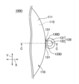
図1、図2、図3、図4に示すように、本実施形態の支持基板100は、化学蒸着により炭化ケイ素多結晶膜Fを成膜させる成膜対象面111、成膜対象面111に対して裏面となる成膜対象面112を有する被成膜部110と、化学蒸着の際に後述する保持部材1081により保持され、一体化部分130によって被成膜部110と一体化する被保持部120と、を備える。また、本実施形態の支持基板100は、例えば、被保持部120を1つ備えている。なお、図2に示すように、支持基板100において、被成膜部110、一体化部分130及び被保持部120の連なる方向を方向X、被成膜部110の面内で、方向Xに直交する方向を方向Yとする。
As shown in FIGS. 1, 2, 3, and 4, the
また、支持基板100は、例えば、厚さ0.5mm~10mmで平板状に形成することができる。厚さが0.5mmを下回ると、支持基板100の強度が不足しやすく、後述する成膜工程中に落下することがある。また、10mmを超えると、炭化ケイ素多結晶膜Fを成膜した後に支持基板100を除去するときの燃焼や酸を用いた溶解等の処理時間が長くなり、また、材料の無駄となり高コストになるおそれがある。また、支持基板100は、平行平板状のもの、すなわち、図面に示すように、成膜対象面111、112が表面と裏面に相当する平行な平板を好適に用いることができる。なお、本明細書において、平行平板における「平行」は、厳密な平行だけでなく、支持基板100の平行な面を作成する上で不可避な誤差を有する場合も含む。また、支持基板100の材質は、特に限定されず、所望の多結晶膜を成膜させることができる任意の材料を用いることができ、例えば、黒鉛やケイ素を用いることができる。また、支持基板100の材質としては、被保持部120を形成することを考慮して、より加工が容易な黒鉛を好適に用いることができる。
Further, the
被成膜部110は、例えば4インチまたは6インチの円板状であり、所望の大きさの炭化ケイ素多結晶膜Fに応じた大きさに形成されている。また、被保持部120は、外形が被成膜部110よりも小さい円形状であり、円環状の円環部121と、円環部121の内側に形成され、保持部材1081を通すことができる貫通孔122と、を有する。
The film-forming
また、一体化部分130は、被成膜部110と被保持部120との境界部分であり、くびれている。すなわち、図2に示すように、一体化部分130は、一体化部分130の方向Yにおける両端部に形成された一対のくびれ部131を有しており、方向Yにおいて、被保持部120の直径の長さL1が、一体化部分130の寸法L2(一対のくびれ部131同士をつなぐ直線の長さ)よりも大きくなることでくびれ形状となっている。
Further, the
成膜工程後に、保持部材1081と支持基板100は、炭化ケイ素多結晶膜Fが成膜して一体化してしまうため、保持部材1081、ナットN1、ナットN2から支持基板100を分離することは困難である。そこで、一体化部分130で被成膜部110と被保持部120とを分離できれば、後工程に用いる被成膜部110を容易に取り出せる。一体化部分130がくびれていることにより、炭化ケイ素多結晶膜Fを成膜させた後、被成膜部110と被保持部120とを、例えば折り取る等することで分離するときに、一体化部分130に加えられる力がより狭い部分に加わることになる。よって、被成膜部110と被保持部120とを分離しやすくなり、作業性を向上させるとともに、被成膜部110と被保持部120とを分離するときに発生し得る炭化ケイ素多結晶膜Fの割れやクラック等の損傷を防止することができる。
After the film forming process, the holding
また、支持基板100は、一体化部分130において、被成膜部110と被保持部120との境界線132の長さである、一対のくびれ部131同士の間をつなぐ直線の長さL2が、8mm~12mmであることが好ましい。これにより、保持部材1081に保持された状態における、支持基板100が一体化部分130で折れたり、撓んだりすることがない程度の強度と、被成膜部110と被保持部120とを分離するときの分離容易性を両立させることができる。
In addition, in the
本実施形態の支持基板100であれば、支持基板100を1箇所で保持することにより、化学蒸着により成膜したときに、複数箇所の保持では発生頻度が高い場合がある、成膜された炭化ケイ素多結晶膜Fや支持基板100の割れやクラック等の損傷を防止することができる。
In the case of the
(支持基板の保持方法)
次に、本発明の一実施形態にかかる支持基板の保持方法を、図3を参照して説明する。本実施形態では、成膜装置1000における、前述の支持基板100の保持方法を説明する。
(Method for holding support substrate)
Next, a method for holding a support substrate according to one embodiment of the present invention will be described with reference to FIG. In this embodiment, a method for holding the
図3(A)に示すように、成膜装置1000は、化学蒸着により、支持基板100に炭化ケイ素多結晶膜Fを成膜させることができる。成膜装置1000は、成膜装置1000の外装となる筐体1010と、支持基板100に炭化ケイ素多結晶膜Fを成膜させる成膜室1020と、成膜室1020より排出された原料ガスやキャリアガスを後述のガス排出口1040へ導入する排出ガス導入室1050と、排出ガス導入室1050を覆うボックス1060と、ボックス1060の外部より成膜室1020内を加温する、カーボン製のヒーター1070と、成膜室1020の上部に設けられ、成膜室1020に原料ガスやキャリアガスを導入するガス導入口1030と、ガス排出口1040と、支持基板100を保持する基板ホルダー1080を有する。また、基板ホルダー1080は、棒状の保持部材1081と、保持部材1081を成膜室1020内に固定する保持台座1082と、を有する。また、保持台座1082は、成膜室1020の底部に設けられ、保持台座1082には、保持部材1081を挿し込んで固定することができる穴(不図示)が形成されており、棒状の保持部材1081を縦方向に保持することができる。すなわち、支持基板100は、保持部材1081に、成膜対象面111、112が水平方向になるように保持される。また、保持部材1081において、支持基板100が保持される箇所は、後述するナットN1、ナットN2を締結するためのねじ切り加工が施されている。また、保持部材1081、ナットN1、N2の材質としては、特に限定されず、耐熱性や加工性を考慮して、例えば、黒鉛を好適に用いることができる。
As shown in FIG. 3A, the
図3(A)、図3(B)に示すように、支持基板100は、保持部材1081により被保持部120を保持されることで、保持される。作業の手順としては、まず、保持部材1081をナットN1に挿通しておき、支持基板100の貫通孔122に保持部材1081を通し、さらに、保持部材1081をナットN2に挿通する。ナットN1とナットN2により支持基板100の被保持部120を挟み込んで締結することにより、保持部材1081により支持基板100を保持することができる。また、保持部材1081に複数の支持基板100を保持する場合には、上記作業を繰り返して行う。なお、一対のナットN1、ナットN2で支持基板100を挟んで保持部材に支持基板100を保持することができれば、上記作業の順序は変更してもよい。
As shown in FIGS. 3A and 3B, the
また、ナットN1、ナットN2の径寸法は特に限定されないが、被成膜部110に干渉しない、被保持部120と同じ程度の大きさのナットN1、ナットN2を用いることで、被成膜部110と被保持部120との分離が容易となるため、炭化ケイ素多結晶膜Fを支持基板100から燃焼除去等することで得られる炭化ケイ素多結晶基板の歩留まりを向上させることができる。
In addition, although the diameters of the nuts N1 and N2 are not particularly limited, by using the nuts N1 and nuts N2 having approximately the same size as the held
また、1つの保持部材1081に保持する支持基板100の数や成膜室1020内に設置する、支持基板100を保持した保持部材1081の数は特に限定されず、成膜室1020の大きさ等に合わせて適宜変更できる。
Further, the number of supporting
本実施形態の支持基板100の保持方法によれば、被保持部120を保持部材1081により保持することで、支持基板100を従来よりも少ない箇所で保持することとなり、化学蒸着により成膜したときに、複数箇所の保持では発生頻度が高い場合がある、成膜された炭化ケイ素多結晶膜Fや支持基板100の割れやクラック等の損傷を防止することができる。
According to the method for holding the
(成膜方法)
次に、本発明の一実施形態にかかる成膜方法を、図3、図4を参照して説明する。本実施形態では、前述の成膜装置1000を用いて支持基板100に炭化ケイ素多結晶膜Fを成膜する、成膜方法を説明する。以下の説明は成膜方法の一例であり、問題のない範囲で温度、圧力、ガス雰囲気等の各条件や、手順等を変更してもよい。
(Film formation method)
Next, a film forming method according to an embodiment of the present invention will be described with reference to FIGS. 3 and 4. FIG. In this embodiment, a film forming method for forming a silicon carbide polycrystalline film F on the
本実施形態の成膜方法は、前述の保持方法により、保持部材1081に保持された支持基板100に、化学蒸着により炭化ケイ素多結晶膜Fを成膜する成膜工程を含む。
The film forming method of the present embodiment includes a film forming step of forming a silicon carbide polycrystalline film F by chemical vapor deposition on the supporting
成膜工程について説明する。まず、支持基板100を保持した状態で、減圧状態で、Ar等の不活性ガス雰囲気下で、成膜の反応温度まで、ヒーター1070により支持基板100を加熱する。成膜の反応温度(例えば、1200℃程度)まで達したら、不活性ガスの供給を止めて、成膜室1020内に炭化ケイ素多結晶膜Fの成分を含む原料ガスやキャリアガスを供給する。
A film forming process will be described. First, with the supporting
原料ガスとしては、炭化ケイ素多結晶膜Fを成膜させることができれば、特に限定されず、一般的に炭化ケイ素多結晶膜の成膜に使用されるSi系原料ガス、C系原料ガスを用いることができる。例えば、Si系原料ガスとしては、シラン(SiH4)を用いることができるほか、モノクロロシラン(SiH3Cl)、ジクロロシラン(SiH2Cl2)、トリクロロシラン(SiHCl3)、テトラクロロシラン(SiCl4)などのエッチング作用があるClを含む塩素系Si原料含有ガス(クロライド系原料)を用いることができる。C系原料ガスとしては、例えば、メタン(CH4)、プロパン(C3H8)、アセチレン(C2H2)等の炭化水素を用いることができる。上記のほか、トリクロロメチルシラン(CH3Cl3Si)、トリクロロフェニルシラン(C6H5Cl3Si)、ジクロロメチルシラン(CH4Cl2Si)、ジクロロジメチルシラン((CH3)2SiCl2)、クロロトリメチルシラン((CH3)3SiCl)等のSiとCとを両方含むガスも、原料ガスとして用いることができる。 The raw material gas is not particularly limited as long as the silicon carbide polycrystalline film F can be formed, and Si-based raw material gas and C-based raw material gas generally used for forming a silicon carbide polycrystalline film are used. be able to. For example, as the Si-based source gas, silane (SiH 4 ) can be used, as well as monochlorosilane (SiH 3 Cl), dichlorosilane (SiH 2 Cl 2 ), trichlorosilane (SiHCl 3 ), tetrachlorosilane (SiCl 4 ) can be used. Hydrocarbons such as methane (CH 4 ), propane (C 3 H 8 ), and acetylene (C 2 H 2 ) can be used as the C source gas. In addition to the above, trichloromethylsilane (CH 3 Cl 3 Si), trichlorophenylsilane (C 6 H 5 Cl 3 Si), dichloromethylsilane (CH 4 Cl 2 Si), dichlorodimethylsilane ((CH 3 ) 2 SiCl 2 ), chlorotrimethylsilane ((CH 3 ) 3 SiCl), and other gases containing both Si and C can also be used as source gases.
また、キャリアガスとしては、炭化ケイ素多結晶膜Fの成膜を阻害することなく、原料ガスを支持基板100へ展開することができれば、一般的に使用されるキャリアガスを用いることができる。例えば、熱伝導率に優れ、炭化ケイ素に対してエッチング作用があるH2ガスをキャリアガスとして用いることができる。また、これら原料ガスおよびキャリアガスと同時に、第3のガスとして、不純物ドーピングガスを同時に供給することもできる。例えば、炭化ケイ素多結晶膜Fを支持基板100から分離することで得られる炭化ケイ素多結晶基板の導電型をn型とする場合には窒素(N2)、p型とする場合にはトリメチルアルミニウム(TMA)を用いることができる。
Further, as the carrier gas, a commonly used carrier gas can be used as long as the source gas can be spread over the
炭化ケイ素多結晶膜Fを成膜させる際には、上記のガスを適宜混合して供給する。また、所望の炭化ケイ素多結晶膜Fの性状に応じて、成膜工程の途中でガスの混合割合、供給量等の条件を変更してもよい。 When forming the silicon carbide polycrystalline film F, the above gases are appropriately mixed and supplied. In addition, depending on the properties of the desired polycrystalline silicon carbide film F, the conditions such as the mixing ratio of the gas and the amount of supply may be changed during the film forming process.
また、炭化ケイ素以外を成膜する場合には、成膜する多結晶に応じてガス、温度、圧力、時間等の成膜条件を設定することができる。窒化チタンの多結晶膜を形成する場合には、TiCl4ガス、N2ガス等を用いることができる。窒化アルミニウムの多結晶膜を形成する場合には、AlCl3ガス、NH3ガス等を用いることができる。炭化チタンの多結晶膜を形成する場合には、TiCl4ガス、CH4ガス等を用いることができる。ダイヤモンドライクカーボンの多結晶膜を形成する場合には、アセチレン等の炭化水素ガスを用いることができる。 In the case of depositing a film other than silicon carbide, film deposition conditions such as gas, temperature, pressure, and time can be set according to the polycrystal to be deposited. When forming a polycrystalline film of titanium nitride, TiCl 4 gas, N 2 gas, etc. can be used. When forming a polycrystalline film of aluminum nitride, AlCl 3 gas, NH 3 gas, or the like can be used. When forming a polycrystalline film of titanium carbide, TiCl 4 gas, CH 4 gas, etc. can be used. When forming a polycrystalline film of diamond-like carbon, a hydrocarbon gas such as acetylene can be used.
支持基板100の表面や気相での化学反応により、加熱した支持基板100の両面に炭化ケイ素多結晶膜Fを成膜させることができる。これにより、図4に示すように、支持基板100に炭化ケイ素多結晶膜Fが成膜された、蒸着物が得られる。なお、成膜工程後は、図4に示すように、支持基板100だけではなく、ナットN1、ナットN2、保持部材1081の周囲にも炭化ケイ素多結晶膜Fが成膜している。
A silicon carbide polycrystalline film F can be formed on both surfaces of the
本実施形態の成膜方法は、上記の成膜工程後、被成膜部110と被保持部120とを分離する分離工程を含んでいてもよい。
The film forming method of the present embodiment may include a separating step of separating the
分離工程は、上記成膜工程後、被成膜部110と被保持部120とを一体化する一体化部分130に力を加えて、炭化ケイ素多結晶膜Fが成膜した被成膜部110を折り取ること等により、被成膜部110と被保持部120とを分離する工程である。
In the separation step, after the film formation step, force is applied to the
分離工程の後は、支持基板100を除去することにより、炭化ケイ素多結晶基板を得ることができる。支持基板100は、例えば、黒鉛製の支持基板100を用いた場合には、O2や空気等の酸化性ガス雰囲気下で数百度に加熱して、支持基板100のみを燃焼させることにより、支持基板100を除去することができる。また、例えば、ケイ素製の支持基板100を用いた場合には、硝フッ酸(硝酸とフッ化水素酸の混合酸)に浸漬して、支持基板100のみを溶解することで、支持基板100を除去することができる。
After the separation step, the silicon carbide polycrystalline substrate can be obtained by removing the
また、本実施形態の成膜方法によれば、多数箇所(例えば、4箇所)の保持では発生頻度が高い場合がある、成膜された炭化ケイ素多結晶膜Fや支持基板100の割れやクラック等の損傷を防止することができる。
Moreover, according to the film forming method of the present embodiment, cracks and cracks in the formed polycrystalline silicon carbide film F and the supporting
なお、本発明は、前述した実施形態に限定されるものではなく、本発明の目的が達成できる他の工程等を含み、以下に示すような変形等も本発明に含まれる。なお、以下の変形例において、前述した実施形態と同じ構成には同じ符号を付して説明を省略する。 It should be noted that the present invention is not limited to the above-described embodiments, but includes other processes and the like that can achieve the object of the present invention, and the following modifications and the like are also included in the present invention. In addition, in the following modification, the same code|symbol is attached|subjected to the same structure as embodiment mentioned above, and description is abbreviate|omitted.
前述した実施形態においては、支持基板100の被保持部120には貫通孔122が形成されていたが、図5、図6に示すように、支持基板の被保持部が貫通孔を有していなくてもよい。
In the above-described embodiment, the held
[第2実施形態]
図5(A)に示す、支持基板100Aは、被成膜部110と、被保持部120Aと、被成膜部110と被保持部120Aとを一体化する一体化部分130と、を備える。被保持部120Aは、被成膜部110と同じ厚さを有し、成膜対象面111、112と面一の面が四角状である。図5(B)は、支持基板100Aを保持部材1081に保持した状態の一部を示す斜視図である。図5(B)に示すように、支持基板100Aは、保持部材1081を挿通したナットN1、ナットN2の間に被保持部120Aを挿し込んで保持部材1081に被保持部120Aの先端120A1を当接させて、上下よりナットN1、ナットN2を締結することで、保持部材1081に保持することができる。
[Second embodiment]
A
[第3実施形態]
図6(A)に示す、支持基板100Bは、被成膜部110と、被保持部120Bと、被成膜部110と被保持部120Bとを一体化する一体化部分130と、を備える。被保持部120Bは、被成膜部110と同じ厚さを有し、成膜対象面111、112と面一の面が円形状である。すなわち、第1実施形態と同様に、一体化部分130はくびれている。図6(B)は、支持基板100Bを保持部材1081に保持した状態の一部を示す斜視図である。図6(B)に示すように、支持基板100Bは、保持部材1081を挿通したナットN1、ナットN2の間に被保持部120Bを挿し込んで保持部材1081に被保持部120Bの先端120B1を当接させて、上下よりナットN1、ナットN2を締結することで、保持部材1081に保持することができる。また、被保持部120Bが円形状に形成されており、一体化部分130がくびれていることから、被成膜部110と被保持部120Bとを、例えば折り取る等することで分離するときに、被成膜部110と被保持部120Bとをより容易に分離することができる。
[Third embodiment]
A
[第4実施形態]
また、図7に示すように、支持基板100Cの被保持部120Cが二又状に形成されていてもよい。支持基板100Cは、被成膜部110と、被保持部120Cと、被成膜部110と被保持部120Cとを一体化する一体化部分130と、を備える。被保持部120Cは、一体化部分130と連なる側とは反対側が開いた、二又状の両端120C2、120C3によって、平面視半円環状に形成されている。被保持部120Cの二又状の両端120C2、120C3をつなぐ内縁部120C1は、保持部材1081の外周と対応可能な略半円状に形成されている。
[Fourth embodiment]
Further, as shown in FIG. 7, the held
支持基板100Cは、保持部材1081を挿通したナットN1、ナットN2の間に被保持部120Cを挿し込んで保持部材1081の外周に被保持部120Cの内縁部120C1を当接させて、ナットN1、ナットN2を締結することで、保持部材1081に保持することができる。また、被保持部120Cが半円環状に形成されており、一体化部分130がくびれていることから、被成膜部110と被保持部120Cとを分離するときに、被成膜部110と被保持部120Cとをより容易に分離することができる。なお、内縁部120C1は、保持部材1081の外周よりも大きい形状に形成されていてもよく、このとき、保持部材1081の外周に被保持部120Cの内縁部120C1の一部を当接させて、保持部材1081に支持基板100Cを保持させることができる。
The
以上のように、支持基板100Cの被保持部120Cが二又状に形成されていることにより、ナットN1、ナットN2により締結される被保持部120Cの面積が、前述した第2実施形態の支持基板100Aの被保持部120Aや第3実施形態の支持基板100Bの被保持部120Bよりも大きくなるため、より確実な支持基板100Cの保持が可能となる。また、支持基板の貫通孔等に保持部材1081を通す作業を省略することができ、作業性を向上させることができる。
As described above, since the held
[第5実施形態]
また、図8に示す支持基板100Dのように、支持基板は、一体化部分130Dに、被保持部120と被成膜部110との分離がより容易となるように、溝133Dを有していてもよい。
[Fifth embodiment]
Further, like the
支持基板100Dは、被成膜部110と、被保持部120と、被成膜部110と被保持部120とを一体化する一体化部分130Dと、を備える。一体化部分130Dには、方向Yに沿って、2箇所のくびれ131をつなぐ直線状であって、支持基板100の表面から厚さ方向に、溝133Dが形成されている。図9(A)は、図8に示した支持基板100Dの矢視C-C断面を示す一部断面図である。図9(A)に示すように、溝133Dは、等幅で、支持基板100Dの厚さ方向に向かって形成されている。
The
支持基板100Dは、支持基板100Dの一体化部分130Dに、被保持部120と被成膜部110とを分離可能な溝133Dを有している。このことから、被成膜部110と被保持部120とを分離するとき、すなわち、炭化ケイ素多結晶膜Fが成膜した被成膜部110を折り取る等するときに、溝133Dに沿って力が加わりやすくなり、所望の位置で被成膜部110を分離しやすくなる。また、溝133Dが形成された箇所の厚さが薄くなることにより、被成膜部110と被保持部120とをより容易に分離することができる。
The
また、図9(B)、図9(C)に示すように、一体化部分に形成された溝が、くさび状であってもよい。 Also, as shown in FIGS. 9B and 9C, the grooves formed in the integrated portion may be wedge-shaped.
[第6実施形態]
図9(B)に示す支持基板100Eは、被成膜部110と、被保持部120と、被成膜部110と被保持部120とを一体化する一体化部分130Eと、を備え、一体化部分130Eには、くさび状の溝133Eが形成されている。すなわち、支持基板100Eは、溝133Eの形状のみが支持基板100Dと異なる。溝133Dは、支持基板100Eの厚さ方向に向かって溝133Dの幅が徐々に狭くなるように、形成されている。
[Sixth Embodiment]
The
支持基板100Eの一体化部分130Eに形成された溝133Eがくさび状であることから、被成膜部110と被保持部120とを分離するときとき、すなわち、炭化ケイ素多結晶膜Fが成膜した被成膜部110を折り取る等するときに、加えられた力が溝133Eの先端部分132E1に集中しやすくなる。このことから、支持基板100Dと比べて、被成膜部110と被保持部120とをさらに容易に分離することができる。
Since the
[第7実施形態]
図9(C)に示す支持基板100Fは、被成膜部110と、被保持部120と、被成膜部110と被保持部120とを一体化する一体化部分130Fと、を備え、一体化部分130Fには、支持基板100Fの両面から形成された2つのくさび状の溝133Fが形成されている。すなわち、支持基板100Fは、溝133Fが支持基板100Fの両面から形成されている点が支持基板100Eと異なる。
[Seventh embodiment]
A
溝133Fが、支持基板100Fの両面から形成されていることから、被成膜部110と被保持部120とを分離するときに、被成膜部110と被保持部120とをさらに容易に分離することができる。
Since the
[第8実施形態]
また、図10に示すように、支持基板は、一体化部分に、被成膜部と被保持部との境界線132Gに沿ってミシン目状に形成された、複数の貫通孔を有していてもよい。
[Eighth embodiment]
Further, as shown in FIG. 10, the supporting substrate has a plurality of perforated through-holes formed in the integrated portion along the
支持基板100Gは、被成膜部110と、被保持部120Gと、被成膜部110と被保持部120Gとを一体化する一体化部分130Gと、を備える。被保持部120Gは、被成膜部110と同じ厚さを有し、成膜対象面111、112と面一の面が四角状である。また、一体化部分130Gには、被成膜部110と被保持部120との境界線132Gに沿ってミシン目状に形成された、複数の貫通孔133Gが形成されている。
The
被成膜部110と被保持部120との境界線132Gに沿ってミシン目状に形成された、複数の貫通孔133Gが形成されていることから、被成膜部110と被保持部120とを分離するときに、炭化ケイ素多結晶膜Fが成膜した被成膜部110を折り取る等するときに、貫通孔133Gが形成された部分が折り取りやすくなり、被成膜部110と被保持部120とを容易に分離することができる。
Since a plurality of perforated through
[第9実施形態]
前述した支持基板の保持方法の実施形態においては、支持基板100が、保持部材1081に、成膜対象面111、112が水平方向になるように保持されていたが、成膜対象面111、112の保持方向は特に限定されるものではなく、例えば、成膜対象面111、112が鉛直方向になるように支持基板100が保持されてもよい。
[Ninth Embodiment]
In the embodiment of the supporting substrate holding method described above, the supporting
図11は、成膜装置1000とは異なる基板ホルダーを有する成膜装置1000Aを示す図である。
FIG. 11 is a diagram showing a
成膜装置1000Aの基板ホルダー1080Aは、棒状の保持部材1081と、保持部材1081を成膜室1020内に固定する2つの保持台座1082Aと、を有する。また、保持台座1082は、成膜室1020の側壁の内側の2箇所に設けられ、保持台座1082Aには、保持部材1081を挿し込んで固定することができる穴(不図示)が形成されており、棒状の保持部材1081の長手方向を水平に保持することができる。すなわち、成膜装置1000Aにおいて、支持基板100は、保持部材1081に、成膜対象面111、112が鉛直方向になるように保持される。
A
[第10実施形態]
また、特に、支持基板の成膜対象面が鉛直方向になるように保持される場合、図12に示すように、支持基板の被保持部がフック状に形成されていてもよい。
[Tenth embodiment]
In particular, when the supporting substrate is held so that the film formation target surface is vertical, the held portion of the supporting substrate may be formed in a hook shape, as shown in FIG. 12 .
図12に示す支持基板100Hは、被成膜部110と、被保持部120Hと、被成膜部110と被保持部120Hとを一体化する一体化部分130と、を備える。被保持部120Hは、フック状、すなわち、円環の一部が開いたアーチ状に形成されており、被保持部120Hの一方の端部120H1が一体化部分130に連なっている。また、被保持部120Hは、一方の端部120H1と他方の端部120H2とをつなぐ内縁部120H3が、保持部材1081の外周と対応可能な形状に形成されている。
The
支持基板100Hは、ナットN1、ナットN2に挿通させた保持部材1081を保持台座1082Aに固定し、保持部材1081のナットN1、ナットN2の間の部分にフック状の被保持部120Hを引っかけて、被保持部120Hの内縁部120H3を保持部材1081に当接させる。さらに、ナットN1、ナットN2を締結することにより、支持基板100Hを保持部材1081に保持することができる。また、被保持部120Hがフック状であることから、ナットN1、ナットN2の締結が不十分な場合であっても、支持基板100Hが落下することを防止することができる。なお、支持基板100Hは、図3に示したように、成膜対象面111、112が水平になるように保持することもできる。
The
以上のように、支持基板100Hの被保持部120Hがフック状に形成されていることにより、支持基板の貫通孔等に保持部材1081を通す作業を省略することができ、作業性を向上させることができる。
As described above, since the held
上記に一体化部分の形状について種々の変形例を示したように、支持基板の大きさ、厚さ等の形状や成膜条件により必要な一体化部分の強度や、支持基板を保持するときの作業性等を考慮して、一体化部分の形状を設定することができる。 As described above, various modifications of the shape of the integrated portion are required. The shape of the integrated portion can be set in consideration of workability and the like.
なお、上記の実施形態(図1~図12)では、支持基板を1箇所で保持する態様を説明したが、本発明はこれに限定されず、例えば、2、3箇所の保持等の複数保持も可能である。 In the above-described embodiments (FIGS. 1 to 12), the supporting substrate is held at one position, but the present invention is not limited to this. is also possible.
以下、本発明の実施例および比較例によって、本発明をさらに詳細に説明するが、本発明は、これらの実施例によって何ら限定されることはない。 EXAMPLES Hereinafter, the present invention will be described in more detail with reference to Examples and Comparative Examples of the present invention, but the present invention is not limited by these Examples.
本実施例においては、前述した実施形態の支持基板100を保持部材1081に保持し、成膜装置1000を用いて炭化ケイ素多結晶膜Fを成膜する成膜工程を行った。
In this example, the
(実施例1)
支持基板100として、直径151mm、厚さ1000μmの平行平板状の黒鉛基板を用いた。保持部材1081をナットN1に挿通しておき、支持基板100の貫通孔122に保持部材1081を通し、さらに、保持部材1081をナットN2に挿通した。ナットN1とナットN2により支持基板100の被保持部120を挟み込んで締結して、保持部材1081により支持基板100を保持した。支持基板100を保持した保持部材1081を成膜室1020内の保持台座1082に固定した。成膜室1020内に50枚の支持基板100を保持して、1回の成膜工程により50枚の支持基板100に炭化ケイ素多結晶膜Fを成膜させた。
(Example 1)
As the supporting
次に、成膜工程を行った。成膜室1020内を不図示の排気ポンプにより真空引きをした後、1350℃まで加熱した。原料ガスとして、SiCl4、CH4を用い、キャリアガスとしてH2を用い、不純物ドーピングガスとしてN2を用いた。炭化ケイ素多結晶膜の成膜は、SiCl4:CH4:H2:N2=1:1:10:10の比率で上記ガスを混合して成膜室1020内に供給し、40時間の成膜を実施し、2mmの厚さに炭化ケイ素多結晶膜Fを成膜した。このときの炉内圧力は30kPaであった。以上により成膜工程が終了し、50枚の支持基板100から、100枚の炭化ケイ素多結晶膜Fが得られた。成膜工程終了後、成膜装置1000内を徐冷して、成膜装置1000から炭化ケイ素多結晶膜Fが成膜された支持基板100を取り出した。さらに、炭化ケイ素多結晶膜Fに割れやクラック等の損傷が生じているかを、目視において確認した。損傷の確認をしたところ、得られた炭化ケイ素多結晶膜F100枚において、割れやクラック等の損傷が生じたのは0枚であった。
Next, a film forming process was performed. After the
次に、支持基板100の被成膜部110と被保持部120とを分離する分離工程を行った。分離工程は、一体化部分130に力を加え、炭化ケイ素多結晶膜Fが成膜した被成膜部110ごと折り取ることにより行った。さらに、炭化ケイ素多結晶膜Fに割れやクラック等の損傷が生じているかを、目視において確認した。損傷の確認をしたところ、得られた炭化ケイ素多結晶膜F100枚において、割れやクラック等の損傷が生じた炭化ケイ素多結晶膜Fは0枚であった。さらに、炭化ケイ素多結晶膜Fが成膜した被成膜部110を酸素雰囲気下で800℃に加熱して、被成膜部110を燃焼除去した後の炭化ケイ素多結晶膜Fにも、割れやクラック等の損傷は認められなかった。
Next, a separation step was performed to separate the film-forming
(比較例1)
比較例1として、4本の黒鉛製の保持部材を有する基板ホルダーと、被成膜部のみであり、被保持部を有しない、通常用いられる円形の平行平板状の黒鉛製の支持基板500を用いた。その他の構成は図13(A)に示す従来の成膜装置5000と同じものを用いた。図13(B)に示すように、支持基板は、4本の保持部材をそれぞれ黒鉛製の2つのナットに挿通させておき、2つのナットの間に支持基板を挟んでナットを締結させることにより、保持部材に保持した。また、炭化ケイ素多結晶膜の成膜条件は実施例1と同様にして行った。
(Comparative example 1)
As Comparative Example 1, a substrate holder having four holding members made of graphite, and a
成膜装置5000から取り出した炭化ケイ素多結晶膜に割れやクラック等の損傷が生じているかを、目視において確認した。損傷の確認をしたところ、得られた炭化ケイ素多結晶膜100枚において、20枚の炭化ケイ素多結晶膜に割れやクラック等の損傷が生じていた。
It was visually confirmed whether the silicon carbide polycrystalline film taken out from the
本発明の例示的態様である実施例1の支持基板であれば、化学蒸着により成膜したときに、成膜された膜や支持基板の割れやクラック等の損傷を防止することができることが示された。また、被保持部との分離工程や被成膜部の除去処理によっても、成膜された膜に、新たに割れやクラック等の損傷は認められなかった。 It has been shown that the support substrate of Example 1, which is an exemplary embodiment of the present invention, can prevent damage such as cracks and cracks in the formed film and the support substrate when the film is formed by chemical vapor deposition. was done. In addition, no new damage such as cracks or cracks was observed in the deposited film even after the process of separating from the held portion and the removal of the film-forming portion.
100 支持基板
110 被成膜部
120 被保持部
130 一体化部分
111、112 成膜対象面
122 貫通孔
131 くびれ部
132、132G 境界線
133D、133E、133F 溝
133G 貫通孔
1081 保持部材
100
Claims (9)
前記被保持部が、前記保持部材を通すことができる貫通孔を有する、またはフック状である、支持基板。 A film-forming portion having a film-forming target surface by chemical vapor deposition, and a held portion held by a holding member during chemical vapor deposition and integrated with the film-forming portion by an integrated portion ,
The supporting substrate, wherein the held portion has a through-hole through which the holding member can pass, or is hook-shaped .
Priority Applications (1)
| Application Number | Priority Date | Filing Date | Title |
|---|---|---|---|
| JP2019062606A JP7279465B2 (en) | 2019-03-28 | 2019-03-28 | SUPPORTING SUBSTRATE, SUPPORTING SUBSTRATE HOLDING METHOD, AND FILM-FORMING METHOD |
Applications Claiming Priority (1)
| Application Number | Priority Date | Filing Date | Title |
|---|---|---|---|
| JP2019062606A JP7279465B2 (en) | 2019-03-28 | 2019-03-28 | SUPPORTING SUBSTRATE, SUPPORTING SUBSTRATE HOLDING METHOD, AND FILM-FORMING METHOD |
Publications (2)
| Publication Number | Publication Date |
|---|---|
| JP2020158870A JP2020158870A (en) | 2020-10-01 |
| JP7279465B2 true JP7279465B2 (en) | 2023-05-23 |
Family
ID=72642052
Family Applications (1)
| Application Number | Title | Priority Date | Filing Date |
|---|---|---|---|
| JP2019062606A Active JP7279465B2 (en) | 2019-03-28 | 2019-03-28 | SUPPORTING SUBSTRATE, SUPPORTING SUBSTRATE HOLDING METHOD, AND FILM-FORMING METHOD |
Country Status (1)
| Country | Link |
|---|---|
| JP (1) | JP7279465B2 (en) |
Citations (6)
| Publication number | Priority date | Publication date | Assignee | Title |
|---|---|---|---|---|
| JP2006310702A (en) | 2005-05-02 | 2006-11-09 | Sharp Corp | Substrate supporting method and semiconductor substrate |
| JP2008177411A (en) | 2007-01-19 | 2008-07-31 | Mitsubishi Electric Corp | Power semiconductor device having breaking mechanism |
| JP2010185091A (en) | 2009-02-10 | 2010-08-26 | Toyo Tanso Kk | Cvd apparatus |
| JP2013077655A (en) | 2011-09-29 | 2013-04-25 | Toshiba Corp | Semiconductor device and semiconductor manufacturing apparatus |
| WO2015182552A1 (en) | 2014-05-28 | 2015-12-03 | 京セラ株式会社 | Cutting insert manufacturing method |
| JP2016503238A (en) | 2012-12-31 | 2016-02-01 | サンエディソン・セミコンダクター・リミテッドSunEdison Semiconductor Limited | Equipment for applying stress to semiconductor substrates |
Family Cites Families (1)
| Publication number | Priority date | Publication date | Assignee | Title |
|---|---|---|---|---|
| JPH03138366A (en) * | 1989-10-24 | 1991-06-12 | Pioneer Electron Corp | Holding mechanism for material to be vapor-deposited in vapor deposition apparatus |
-
2019
- 2019-03-28 JP JP2019062606A patent/JP7279465B2/en active Active
Patent Citations (6)
| Publication number | Priority date | Publication date | Assignee | Title |
|---|---|---|---|---|
| JP2006310702A (en) | 2005-05-02 | 2006-11-09 | Sharp Corp | Substrate supporting method and semiconductor substrate |
| JP2008177411A (en) | 2007-01-19 | 2008-07-31 | Mitsubishi Electric Corp | Power semiconductor device having breaking mechanism |
| JP2010185091A (en) | 2009-02-10 | 2010-08-26 | Toyo Tanso Kk | Cvd apparatus |
| JP2013077655A (en) | 2011-09-29 | 2013-04-25 | Toshiba Corp | Semiconductor device and semiconductor manufacturing apparatus |
| JP2016503238A (en) | 2012-12-31 | 2016-02-01 | サンエディソン・セミコンダクター・リミテッドSunEdison Semiconductor Limited | Equipment for applying stress to semiconductor substrates |
| WO2015182552A1 (en) | 2014-05-28 | 2015-12-03 | 京セラ株式会社 | Cutting insert manufacturing method |
Also Published As
| Publication number | Publication date |
|---|---|
| JP2020158870A (en) | 2020-10-01 |
Similar Documents
| Publication | Publication Date | Title |
|---|---|---|
| TWI355685B (en) | Epitaxial deposition process and apparatus | |
| EP2099063B1 (en) | Film forming apparatus and method of forming film | |
| WO2009116233A1 (en) | Silicon epitaxial wafer and method for manufacturing the same | |
| KR102294324B1 (en) | Method and device for producing coated semiconductor wafers | |
| JP7279465B2 (en) | SUPPORTING SUBSTRATE, SUPPORTING SUBSTRATE HOLDING METHOD, AND FILM-FORMING METHOD | |
| JP7163756B2 (en) | LAMINATED PRODUCT, METHOD FOR MANUFACTURING LAMINATED BODY, AND METHOD FOR MANUFACTURING SILICON CARBIDE POLYCRYSTALLINE SUBSTRATE | |
| JP7220845B2 (en) | Susceptor, susceptor regeneration method, and film formation method | |
| JP7294021B2 (en) | Method for surface treatment of graphite support substrate, method for depositing polycrystalline silicon carbide film, and method for manufacturing polycrystalline silicon carbide substrate | |
| JP7255473B2 (en) | Method for manufacturing polycrystalline silicon carbide substrate | |
| JP7400337B2 (en) | Method for manufacturing silicon carbide polycrystalline substrate | |
| JP7273267B2 (en) | Method for manufacturing polycrystalline silicon carbide substrate | |
| JP7220844B2 (en) | Manufacturing method of SiC polycrystalline substrate | |
| JP7247749B2 (en) | Silicon carbide polycrystalline film deposition method, susceptor, and deposition apparatus | |
| JP7247819B2 (en) | Method for manufacturing polycrystalline silicon carbide substrate | |
| JP2013035731A (en) | Manufacturing method for single crystal silicon carbide film and manufacturing method for substrate with single crystal silicon carbide film | |
| JP7338193B2 (en) | Method for manufacturing polycrystalline silicon carbide substrate | |
| JP7413768B2 (en) | Method for manufacturing polycrystalline substrate | |
| JP7367541B2 (en) | Method for manufacturing silicon carbide polycrystalline substrate | |
| JP7371510B2 (en) | Film formation method and substrate manufacturing method | |
| JP7322371B2 (en) | Method for manufacturing polycrystalline silicon carbide substrate | |
| JP7135718B2 (en) | Substrate holding mechanism, deposition apparatus, and method for depositing polycrystalline film | |
| KR102417484B1 (en) | Epitaxial wafer and method for fabricating the same | |
| JP7367497B2 (en) | Method for forming a silicon carbide polycrystalline film and manufacturing method for a silicon carbide polycrystalline substrate | |
| JP7322408B2 (en) | Polycrystalline silicon carbide substrate, method for producing polycrystalline silicon carbide film, and method for producing polycrystalline silicon carbide substrate | |
| KR20040100937A (en) | Method for processing a surface, method for making a silicon epitaxial wafer and a silicon epitaxial wafer |
Legal Events
| Date | Code | Title | Description |
|---|---|---|---|
| A621 | Written request for application examination |
Free format text: JAPANESE INTERMEDIATE CODE: A621 Effective date: 20211224 |
|
| A977 | Report on retrieval |
Free format text: JAPANESE INTERMEDIATE CODE: A971007 Effective date: 20221124 |
|
| A131 | Notification of reasons for refusal |
Free format text: JAPANESE INTERMEDIATE CODE: A131 Effective date: 20221129 |
|
| A521 | Request for written amendment filed |
Free format text: JAPANESE INTERMEDIATE CODE: A523 Effective date: 20230125 |
|
| TRDD | Decision of grant or rejection written | ||
| A01 | Written decision to grant a patent or to grant a registration (utility model) |
Free format text: JAPANESE INTERMEDIATE CODE: A01 Effective date: 20230411 |
|
| A61 | First payment of annual fees (during grant procedure) |
Free format text: JAPANESE INTERMEDIATE CODE: A61 Effective date: 20230424 |
|
| R150 | Certificate of patent or registration of utility model |
Ref document number: 7279465 Country of ref document: JP Free format text: JAPANESE INTERMEDIATE CODE: R150 |