JP7264249B2 - LC filter - Google Patents
LC filter Download PDFInfo
- Publication number
- JP7264249B2 JP7264249B2 JP2021530531A JP2021530531A JP7264249B2 JP 7264249 B2 JP7264249 B2 JP 7264249B2 JP 2021530531 A JP2021530531 A JP 2021530531A JP 2021530531 A JP2021530531 A JP 2021530531A JP 7264249 B2 JP7264249 B2 JP 7264249B2
- Authority
- JP
- Japan
- Prior art keywords
- capacitor
- electrode
- via conductor
- capacitor electrode
- electrodes
- Prior art date
- Legal status (The legal status is an assumption and is not a legal conclusion. Google has not performed a legal analysis and makes no representation as to the accuracy of the status listed.)
- Active
Links
Images


Classifications
-
- H—ELECTRICITY
- H03—ELECTRONIC CIRCUITRY
- H03H—IMPEDANCE NETWORKS, e.g. RESONANT CIRCUITS; RESONATORS
- H03H7/00—Multiple-port networks comprising only passive electrical elements as network components
- H03H7/01—Frequency selective two-port networks
- H03H7/0115—Frequency selective two-port networks comprising only inductors and capacitors
-
- H—ELECTRICITY
- H03—ELECTRONIC CIRCUITRY
- H03H—IMPEDANCE NETWORKS, e.g. RESONANT CIRCUITS; RESONATORS
- H03H7/00—Multiple-port networks comprising only passive electrical elements as network components
- H03H7/01—Frequency selective two-port networks
- H03H7/09—Filters comprising mutual inductance
-
- H—ELECTRICITY
- H01—ELECTRIC ELEMENTS
- H01F—MAGNETS; INDUCTANCES; TRANSFORMERS; SELECTION OF MATERIALS FOR THEIR MAGNETIC PROPERTIES
- H01F27/00—Details of transformers or inductances, in general
-
- H—ELECTRICITY
- H01—ELECTRIC ELEMENTS
- H01G—CAPACITORS; CAPACITORS, RECTIFIERS, DETECTORS, SWITCHING DEVICES OR LIGHT-SENSITIVE DEVICES, OF THE ELECTROLYTIC TYPE
- H01G4/00—Fixed capacitors; Processes of their manufacture
- H01G4/40—Structural combinations of fixed capacitors with other electric elements, the structure mainly consisting of a capacitor, e.g. RC combinations
-
- H—ELECTRICITY
- H03—ELECTRONIC CIRCUITRY
- H03H—IMPEDANCE NETWORKS, e.g. RESONANT CIRCUITS; RESONATORS
- H03H7/00—Multiple-port networks comprising only passive electrical elements as network components
- H03H7/01—Frequency selective two-port networks
- H03H7/17—Structural details of sub-circuits of frequency selective networks
- H03H7/1708—Comprising bridging elements, i.e. elements in a series path without own reference to ground and spanning branching nodes of another series path
-
- H—ELECTRICITY
- H03—ELECTRONIC CIRCUITRY
- H03H—IMPEDANCE NETWORKS, e.g. RESONANT CIRCUITS; RESONATORS
- H03H7/00—Multiple-port networks comprising only passive electrical elements as network components
- H03H7/01—Frequency selective two-port networks
- H03H7/17—Structural details of sub-circuits of frequency selective networks
- H03H7/1741—Comprising typical LC combinations, irrespective of presence and location of additional resistors
- H03H7/1766—Parallel LC in series path
-
- H—ELECTRICITY
- H03—ELECTRONIC CIRCUITRY
- H03H—IMPEDANCE NETWORKS, e.g. RESONANT CIRCUITS; RESONATORS
- H03H7/00—Multiple-port networks comprising only passive electrical elements as network components
- H03H7/01—Frequency selective two-port networks
- H03H7/17—Structural details of sub-circuits of frequency selective networks
- H03H7/1741—Comprising typical LC combinations, irrespective of presence and location of additional resistors
- H03H7/1775—Parallel LC in shunt or branch path
-
- H—ELECTRICITY
- H03—ELECTRONIC CIRCUITRY
- H03H—IMPEDANCE NETWORKS, e.g. RESONANT CIRCUITS; RESONATORS
- H03H1/00—Constructional details of impedance networks whose electrical mode of operation is not specified or applicable to more than one type of network
- H03H2001/0021—Constructional details
- H03H2001/0085—Multilayer, e.g. LTCC, HTCC, green sheets
Description
本発明は、複数のLC共振器を備えるLCフィルタに関する。 The present invention relates to an LC filter with multiple LC resonators.
従来、複数のLC共振器を備えるLCフィルタが知られている。たとえば、国際公開第2018/100923号(特許文献1)には、4つのLC共振器の各々が少なくとも他の2つのLC共振器と隣接するように千鳥状に配置されたバンドパスフィルタが開示されている。4つのLC共振器を千鳥状に配置することにより、直線状の配置とするよりもLC共振器間の磁気結合が強まるため、バンドパスフィルタの通過帯域を広げることができる。 LC filters with a plurality of LC resonators are conventionally known. For example, International Publication No. WO2018/100923 (Patent Document 1) discloses a bandpass filter in which each of the four LC resonators is arranged in a staggered manner so that it is adjacent to at least two other LC resonators. ing. By arranging the four LC resonators in a zigzag pattern, the magnetic coupling between the LC resonators is stronger than when they are arranged in a straight line, so that the pass band of the bandpass filter can be widened.
LCフィルタの通過特性は、当該LCフィルタが使用される通信システムに応じて調整される必要がある。たとえば、LCフィルタの通過帯域よりも低い周波数帯(低域側)および当該通過帯域よりも高い周波数帯(高域側)の各々において、減衰極が発生する周波数を調整することにより、当該通過帯域を調整することができる。 The pass characteristic of the LC filter has to be adjusted according to the communication system in which the LC filter is used. For example, by adjusting the frequency at which the attenuation pole occurs in each of the frequency band (lower side) than the passband of the LC filter and the frequency band (higher side) than the passband, the passband can be adjusted.
しかし、特許文献1に開示されている、4つのLC共振器が千鳥状に配置されたバンドパスフィルタの通過特性においては、低域側に減衰極が生じていない。そのため、当該バンドパスフィルタによると、通過特性の調整が限定され、所望の通過特性の実現が困難になり得る。
However, in the pass characteristic of the band-pass filter in which four LC resonators are arranged in a staggered manner, disclosed in
本発明は上記のような課題を解決するためになされたものであり、その目的は、LCフィルタの通過特性の調整を容易化することである。 SUMMARY OF THE INVENTION The present invention has been made to solve the above problems, and its object is to facilitate adjustment of the pass characteristics of an LC filter.
本発明の一実施形態に係るLCフィルタにおいては、複数の誘電体層が積層方向に積層されている。LCフィルタは、第1LC共振器と、第2LC共振器と、第3LC共振器と、第4LC共振器と、第1接地電極とを備える。第1LC共振器は、第1ビア導体と、第1キャパシタ電極とを含む。第1ビア導体は、積層方向に延在する。第1キャパシタ電極は、第1ビア導体の一方端に接続され、積層方向において第1接地電極と対向する。第2LC共振器は、第2ビア導体と、第2キャパシタ電極とを含む。第2ビア導体は、積層方向に延在する。第2キャパシタ電極は、第2ビア導体の一方端に接続され、積層方向において第1接地電極と対向する。第3LC共振器は、第3ビア導体と、第3キャパシタ電極とを含む。第3ビア導体は、積層方向に延在する。第3キャパシタ電極は、第3ビア導体の一方端に接続され、積層方向において第1接地電極と対向する。第4LC共振器は、第4ビア導体と、第4キャパシタ電極とを含む。第4ビア導体は、積層方向に延在する。第4キャパシタ電極は、第4ビア導体の一方端に接続され、積層方向において第1接地電極と対向する。第2キャパシタ電極は、積層方向に直交する方向において、第1キャパシタ電極、第3キャパシタ電極、および第4キャパシタ電極の各々と対向する。 In an LC filter according to one embodiment of the present invention, a plurality of dielectric layers are stacked in the stacking direction. The LC filter includes a first LC resonator, a second LC resonator, a third LC resonator, a fourth LC resonator, and a first ground electrode. The first LC resonator includes a first via conductor and a first capacitor electrode. The first via conductor extends in the stacking direction. The first capacitor electrode is connected to one end of the first via conductor and faces the first ground electrode in the stacking direction. The second LC resonator includes a second via conductor and a second capacitor electrode. The second via conductor extends in the stacking direction. The second capacitor electrode is connected to one end of the second via conductor and faces the first ground electrode in the stacking direction. The third LC resonator includes a third via conductor and a third capacitor electrode. The third via conductor extends in the stacking direction. The third capacitor electrode is connected to one end of the third via conductor and faces the first ground electrode in the stacking direction. A fourth LC resonator includes a fourth via conductor and a fourth capacitor electrode. The fourth via conductor extends in the stacking direction. The fourth capacitor electrode is connected to one end of the fourth via conductor and faces the first ground electrode in the stacking direction. The second capacitor electrode faces each of the first capacitor electrode, the third capacitor electrode, and the fourth capacitor electrode in a direction orthogonal to the stacking direction.
本発明の一実施形態に係るLCフィルタによれば、第2キャパシタ電極が、積層方向に直交する方向において、第1キャパシタ電極、第3キャパシタ電極、および第4キャパシタ電極の各々と対向することにより、LCフィルタの通過特性の調整を容易化することができる。 According to the LC filter according to one embodiment of the present invention, the second capacitor electrode faces each of the first capacitor electrode, the third capacitor electrode, and the fourth capacitor electrode in the direction perpendicular to the stacking direction. , the adjustment of the pass characteristic of the LC filter can be facilitated.
以下、実施の形態について図面を参照しながら詳細に説明する。なお、図中同一または相当部分には同一符号を付してその説明は原則として繰り返さない。 Hereinafter, embodiments will be described in detail with reference to the drawings. In the drawings, the same or corresponding parts are denoted by the same reference numerals, and the description thereof will not be repeated in principle.
[実施の形態1]
図1は、実施の形態1に係るLCフィルタの一例であるバンドパスフィルタ1の等価回路図である。図1に示されるように、バンドパスフィルタ1は、入出力端子P1,P2と、LC並列共振器LC1~LC4と、キャパシタC12と、キャパシタC13と、キャパシタC23と、キャパシタC24と、キャパシタC34とを備える。以下では、バンドパスフィルタの使用周波数(たとえば通過帯域の中心周波数)に対応する波長をλとする。なお、実施の形態に係るLCフィルタは、LC直列共振器を含んでもよい。[Embodiment 1]
FIG. 1 is an equivalent circuit diagram of a
LC並列共振器LC1は、入出力端子P1と接続されている。LC並列共振器LC4は、入出力端子P2に接続されている。なお、LC並列共振器LC1は、インダクタあるいはキャパシタなどの素子を介して間接的に入出力端子P1と接続されても良い。同様に、LC並列共振器LC4は、インダクタあるいはキャパシタなどの素子を介して間接的に入出力端子P2と接続されても良い。 The LC parallel resonator LC1 is connected to the input/output terminal P1. The LC parallel resonator LC4 is connected to the input/output terminal P2. Note that the LC parallel resonator LC1 may be indirectly connected to the input/output terminal P1 via an element such as an inductor or a capacitor. Similarly, the LC parallel resonator LC4 may be indirectly connected to the input/output terminal P2 via an element such as an inductor or a capacitor.
LC並列共振器LC2およびLC3は、LC並列共振器LC1とLC4との間に配置されている。LC並列共振器LC1~LC4は、後述する磁気結合および容量結合の強さに応じて順次結合し、4段のLCフィルタを構成する。 LC parallel resonators LC2 and LC3 are arranged between LC parallel resonators LC1 and LC4. The LC parallel resonators LC1 to LC4 are sequentially coupled according to the strength of magnetic coupling and capacitive coupling, which will be described later, to form a four-stage LC filter.
キャパシタC12は、LC並列共振器LC1とLC2との間に接続されている。キャパシタC12は、LC並列共振器LC1とLC2との間の容量結合を表す。 A capacitor C12 is connected between the LC parallel resonators LC1 and LC2. Capacitor C12 represents the capacitive coupling between LC parallel resonators LC1 and LC2.
キャパシタC13は、LC並列共振器LC1とLC3との間に接続されている。キャパシタC13は、LC並列共振器LC1とLC3との間の容量結合を表す。 A capacitor C13 is connected between the LC parallel resonators LC1 and LC3. Capacitor C13 represents the capacitive coupling between LC parallel resonators LC1 and LC3.
キャパシタC23は、LC並列共振器LC2とLC3との間に接続されている。キャパシタC23は、LC並列共振器LC2とLC3との間の容量結合を表す。 A capacitor C23 is connected between the LC parallel resonators LC2 and LC3. Capacitor C23 represents the capacitive coupling between LC parallel resonators LC2 and LC3.
キャパシタC24は、LC並列共振器LC2とLC4との間に接続されている。キャパシタC24は、LC並列共振器LC2とLC4との間の容量結合を表す。 Capacitor C24 is connected between LC parallel resonators LC2 and LC4. Capacitor C24 represents the capacitive coupling between LC parallel resonators LC2 and LC4.
キャパシタC34は、LC並列共振器LC3とLC4との間に接続されている。キャパシタC34は、LC並列共振器LC3とLC4との間の容量結合を表す。 A capacitor C34 is connected between the LC parallel resonators LC3 and LC4. Capacitor C34 represents the capacitive coupling between LC parallel resonators LC3 and LC4.
LC並列共振器LC1(第1LC共振器)は、インダクタL1と、キャパシタC1とを含む。インダクタL1とキャパシタC1とは、接地点と、入出力端子P1およびキャパシタC12の接続点との間において並列に接続されている。 LC parallel resonator LC1 (first LC resonator) includes inductor L1 and capacitor C1. Inductor L1 and capacitor C1 are connected in parallel between a ground point and a connection point between input/output terminal P1 and capacitor C12.
LC並列共振器LC2(第2LC共振器)は、インダクタL2と、キャパシタC2とを含む。インダクタL2とキャパシタC2とは、接地点と、キャパシタC12およびC23の接続点との間において並列に接続されている。 LC parallel resonator LC2 (second LC resonator) includes inductor L2 and capacitor C2. Inductor L2 and capacitor C2 are connected in parallel between the ground point and the connection point of capacitors C12 and C23.
LC並列共振器LC3(第3LC共振器)は、インダクタL3と、キャパシタC3とを含む。インダクタL3とキャパシタC3とは、接地点と、キャパシタC23およびC34の接続点との間において並列に接続されている。 LC parallel resonator LC3 (third LC resonator) includes inductor L3 and capacitor C3. Inductor L3 and capacitor C3 are connected in parallel between the ground point and the connection point of capacitors C23 and C34.
LC並列共振器LC4(第4LC共振器)は、インダクタL4と、キャパシタC4とを含む。インダクタL4とキャパシタC4とは、接地点と、キャパシタC34および入出力端子P2の接続点との間において並列に接続されている。 LC parallel resonator LC4 (fourth LC resonator) includes inductor L4 and capacitor C4. Inductor L4 and capacitor C4 are connected in parallel between the ground point and the connection point between capacitor C34 and input/output terminal P2.
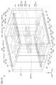
図2は、図1のバンドパスフィルタ1の外観斜視図である。図2において、X軸、Y軸、およびZ軸は互いに直交している。後に説明する図3~図6、図8、図9、図11~図13、図15~図17、図19~図22、図25、図27、および図29においても同様である。
FIG. 2 is an external perspective view of the
図2を参照しながら、バンドパスフィルタ1は、複数の誘電体層がZ軸方向(積層方向)に積層された積層体である。バンドパスフィルタ1は、たとえば直方体状である。Z軸方向に垂直な方向に沿うバンドパスフィルタ1の面を底面BFおよび上面UFとする。積層方向に平行な方向に沿う面のうちYZ平面に沿う面を側面SF1およびSF3とする。積層方向に沿う面のうちZX平面に沿う面を側面SF2およびSF4とする。
Referring to FIG. 2, the
側面SF1には、側面電極105が配置されている。側面電極105は、入出力端子P1を形成する。側面SF3には、側面電極106が配置されている。側面電極106は、入出力端子P2を形成する。
A
底面BFには、接地端子101,102が配置されている。上面UFには、接地端子151,152が配置されている。側面SF2には、側面電極103が配置されている。側面電極103は、接地端子101と151とを接続している。側面SF4には、側面電極104が配置されている。側面電極104は、接地端子102と152とを接続している。接地端子101,102,151,152は、図1の接地点に対応する。
バンドパスフィルタ1の内部には、接地電極111(第1接地電極)と、接地電極141(第2接地電極)とが配置されている。接地電極111は、底面BFに対向している。接地電極141は、上面UFに対向している。接地電極111と141との間には、キャパシタ電極121~124と、ビア導体V1~V4と、平面電極131~134とが配置されている。
Inside the band-
キャパシタ電極121(第1キャパシタ電極)は、側面電極105に接続されている。キャパシタ電極121は、接地電極111と対向している。キャパシタ電極121と接地電極111とは、キャパシタC1を形成する。キャパシタ電極121と接地電極141とは、Z軸方向に延在するビア導体V1(第1ビア導体)によって接続されている。
A capacitor electrode 121 (first capacitor electrode) is connected to the
ビア導体V1は、インダクタL1を形成する。ビア導体V1の一方端はキャパシタ電極121に接続されている。ビア導体V1の一方端は、キャパシタ電極121によって接地電極111から直流的に絶縁された開放端である。LC並列共振器LC1は、λ/4共振器である。ビア導体V1の長さは、ほぼλ/4に等しい。
Via conductor V1 forms inductor L1. One end of via conductor V1 is connected to
キャパシタ電極122(第2キャパシタ電極)は、接地電極111と対向している。キャパシタ電極122と接地電極111とは、キャパシタC2を形成する。キャパシタ電極122と接地電極141とは、Z軸方向に延在するビア導体V2(第2ビア導体)によって接続されている。キャパシタ電極122は、X軸方向においてキャパシタ電極121と対向している。キャパシタ電極121と122とは、キャパシタC12を形成する。
Capacitor electrode 122 (second capacitor electrode) faces
ビア導体V2は、インダクタL2を形成する。ビア導体V2の一方端はキャパシタ電極122に接続されている。ビア導体V2の一方端は、キャパシタ電極122によって接地電極111から直流的に絶縁された開放端である。LC並列共振器LC2は、λ/4共振器である。ビア導体V2の長さは、ほぼλ/4に等しい。
Via conductor V2 forms inductor L2. One end of via conductor V2 is connected to
キャパシタ電極123(第3キャパシタ電極)は、接地電極111と対向している。キャパシタ電極123と接地電極111とは、キャパシタC3を形成する。キャパシタ電極123と接地電極141とは、Z軸方向に延在するビア導体V3(第3ビア導体)によって接続されている。キャパシタ電極123は、Y軸方向においてキャパシタ電極122と対向している。キャパシタ電極122と123とは、キャパシタC23を形成する。キャパシタ電極123は、X軸方向においてキャパシタ電極121と対向している。キャパシタ電極121と123とは、キャパシタC13を形成する。
Capacitor electrode 123 (third capacitor electrode) faces
ビア導体V3は、インダクタL3を形成する。ビア導体V3の一方端はキャパシタ電極123に接続されている。ビア導体V3の一方端は、キャパシタ電極123によって接地電極111から直流的に絶縁された開放端である。LC並列共振器LC3は、λ/4共振器である。ビア導体V3の長さは、ほぼλ/4に等しい。
Via conductor V3 forms inductor L3. One end of via conductor V3 is connected to
キャパシタ電極124(第4キャパシタ電極)は、側面電極106に接続されている。キャパシタ電極124は、接地電極111と対向している。キャパシタ電極124と接地電極111とは、キャパシタC4を形成する。キャパシタ電極124と接地電極141とは、Z軸方向に延在するビア導体V4(第4ビア導体)によって接続されている。キャパシタ電極124は、X軸方向においてキャパシタ電極122および123と対向している。キャパシタ電極122と124とは、キャパシタC24を形成する。キャパシタ電極123と124とは、キャパシタC34を形成する。
A capacitor electrode 124 (fourth capacitor electrode) is connected to the
ビア導体V4は、インダクタL4を形成する。ビア導体V4の一方端はキャパシタ電極124に接続されている。ビア導体V4の一方端は、キャパシタ電極124によって接地電極111から直流的に絶縁された開放端である。LC並列共振器LC4は、λ/4共振器である。ビア導体V4の長さは、ほぼλ/4に等しい。
Via conductor V4 forms inductor L4. One end of via conductor V4 is connected to
平面電極131は、ビア導体V1の両端の間においてビア導体V1に接続されている。平面電極132は、ビア導体V2の両端の間においてビア導体V2に接続されている。平面電極133は、ビア導体V3の両端の間においてビア導体V3に接続されている。平面電極134は、ビア導体V4の両端の間においてビア導体V4に接続されている。
平面電極132の一辺の少なくとも一部は、Y軸方向において平面電極131,134の各々の一辺の少なくとも一部と対向している。平面電極131と132とは、キャパシタC12を形成する。平面電極132と134とは、キャパシタC24を形成する。
At least part of one side of the
平面電極133の一辺の少なくとも一部は、Y軸方向において平面電極131,134の各々の一辺の少なくとも一部と対向している。平面電極131と133とは、キャパシタC13を形成する。平面電極133と134とは、キャパシタC34を形成する。
At least part of one side of the
バンドパスフィルタ1においては、平面電極131~134の各々の形状および配置を変更することにより、キャパシタC12の容量、キャパシタC13の容量、キャパシタC24の容量、およびキャパシタC34の容量の各々を、個別に調整することができる。その結果、バンドパスフィルタ1の特性を所望の特性に高精度に近づけることができる。
In
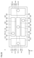
図3は、図2のバンドパスフィルタ1の側面SF1をX軸方向から平面視した図である。図3に示されるように、キャパシタ電極121~124は、誘電体層Ly1に配置されている。キャパシタ電極121~124を同じ誘電体層に形成することにより、バンドパスフィルタ1を低背化することができる。
FIG. 3 is a plan view of the side surface SF1 of the
バンドパスフィルタ1がセラミック多層基板技術を用いて製造される場合、平面方向に複数の同一の配線導体パターンや貫通導体が形成されたセラミックシートを複数層積層し、焼成して積層集合体を形成し、これを平面方向に分割して個々のバンドパスフィルタ1が製造される。或る通信システムに合わせてバンドパスフィルタ1の特性が調整される場合、キャパシタ電極121~124に対応する配線導体パターンの形状および配置を、平面方向に変更した試作用の積層集合体を形成し、これを分割して、個々に特性が異なる複数の試作用のバンドパスフィルタ1が作成される。試作用のバンドパスフィルタ1の中から、必要な特性に合致するバンドパスフィルタ1を抽出し、これと同じ平面電極パターンを量産用のパターンとすることにより、バンドパスフィルタ1の特性の調整を効率化することができる。
When the band-
平面電極131~134は、誘電体層Ly2に配置されている。平面電極131~134を同じ誘電体層に形成することにより、バンドパスフィルタ1を低背化することができる。
The planar electrodes 131-134 are arranged on the dielectric layer Ly2. By forming the
図4は、図2のバンドパスフィルタ1の上面UFをZ軸方向から平面視した図である。図4においては、キャパシタ電極121~124の特徴的な配置を強調するため、平面電極131~134を図示していない。
FIG. 4 is a plan view of the upper surface UF of the
図4に示されるように、ビア導体V2およびV3は、ビア導体V1とV4とを結ぶ仮想線VL1の両側にそれぞれ配置されている。すなわち、ビア導体V1,V4は仮想線VL1上に位置し、ビア導体V2,V3は仮想線VL1上に位置していない。仮想線VL1の一方側にビア導体V2が配置され、他方側にビア導体V3が配置されている。Y軸方向からバンドパスフィルタ1を平面視したとき、ビア導体V2,V3は、ビア導体V1とV4とに挟まれている。
As shown in FIG. 4, via conductors V2 and V3 are arranged on both sides of a virtual line VL1 connecting via conductors V1 and V4. That is, via conductors V1 and V4 are positioned on virtual line VL1, and via conductors V2 and V3 are not positioned on virtual line VL1. A via conductor V2 is arranged on one side of the virtual line VL1, and a via conductor V3 is arranged on the other side. Via conductors V2 and V3 are sandwiched between via conductors V1 and V4 when the
一般に、LC共振器の各々は他のLC共振器と、磁気結合および容量結合により結合する。これらの結合の強さは、各々のLC共振器の形状および位置関係により決定される。磁気結合および容量結合を合わせた総合的な結合の強さに応じて、各LC共振器が順次結合し、LCフィルタを構成する。 In general, each LC resonator is coupled with other LC resonators by magnetic and capacitive coupling. The strength of these couplings is determined by the shape and positional relationship of each LC resonator. Each LC resonator is sequentially coupled according to the total strength of coupling including magnetic coupling and capacitive coupling to form an LC filter.
たとえば、実施の形態1においては磁気結合が容量結合より優位であるとする。ビア導体V1とV2との間の距離は、ビア導体V1とV3との間の距離より短い。そのため、LC並列共振器LC1とLC2との間の磁気結合は、LC並列共振器LC1とLC3との間の磁気結合よりも強い。 For example, assume that magnetic coupling is superior to capacitive coupling in the first embodiment. The distance between via conductors V1 and V2 is shorter than the distance between via conductors V1 and V3. Therefore, the magnetic coupling between the LC parallel resonators LC1 and LC2 is stronger than the magnetic coupling between the LC parallel resonators LC1 and LC3.
ビア導体V4とV3との間の距離は、ビア導体V4とV2との距離より短い。そのため、LC並列共振器LC4とLC3との間の磁気結合は、LC並列共振器LC4とLC2との間の磁気結合よりも強い。この結果、入出力端子P1側から、LC並列共振器LC1、LC並列共振器LC2、LC並列共振器LC3、およびLC並列共振器LC4の順に結合し、4段のLCフィルタが構成される。 The distance between via conductors V4 and V3 is shorter than the distance between via conductors V4 and V2. Therefore, the magnetic coupling between the LC parallel resonators LC4 and LC3 is stronger than the magnetic coupling between the LC parallel resonators LC4 and LC2. As a result, the LC parallel resonator LC1, the LC parallel resonator LC2, the LC parallel resonator LC3, and the LC parallel resonator LC4 are coupled in this order from the input/output terminal P1 side, forming a four-stage LC filter.
キャパシタ電極122,123は、X軸方向においてキャパシタ電極121と124との間に配置されている。キャパシタ電極122,123は、Y軸方向に並置されている。キャパシタ電極121は、キャパシタ電極122,123と隣接している。キャパシタ電極124は、キャパシタ電極122,123と隣接している。すなわち、キャパシタ電極121~124は、千鳥状(ジグザグ状)に配置されている。その結果、図1のLC並列共振器LC1~LC4も、千鳥状に配置される。LC並列共振器LC1~LC4を千鳥状に配置することにより、直線状の配置とするよりもLC並列共振器間の磁気結合が強まる。その結果、インダクタ間の信号伝達が促進され、バンドパスフィルタ1の通過帯域を広げることができる。
キャパシタ電極122は、X軸方向においてキャパシタ電極121および124とそれぞれ対向する外周部F21(第1外周部)、および外周部F23(第3外周部)を有する。キャパシタ電極122は、Y軸方向においてキャパシタ電極123と対向する外周部F22(第2外周部)を有する。
キャパシタ電極は121は、外周部F21と対向する外周部F11(第4外周部)を有する。キャパシタ電極123は、外周部F22と対向する外周部F32(第5外周部)を有する。キャパシタ電極124は、外周部F23と対向する外周部F41(第6外周部)を有する。キャパシタ電極123は、外周部F11およびF41とそれぞれ対向する外周部F31およびF33を有する。
The
外周部F21~F23は、外周部F11、外周部F32、および外周部F41とそれぞれ平行である。外周部F31およびF33は、外周部F11およびF41とそれぞれ平行である。 The outer peripheral portions F21 to F23 are parallel to the outer peripheral portion F11, the outer peripheral portion F32, and the outer peripheral portion F41, respectively. Outer perimeters F31 and F33 are parallel to outer perimeters F11 and F41, respectively.
対向する2つの外周部が平行となるようにキャパシタ電極121~124を配置することにより、対向する2つの外周部を1つのキャパシタにより近い構成とすることができる。その結果、LC共振器間の容量結合を調整し易くなる。なお、実施の形態に係るLCフィルタにおいて対向する2つの外周部は、平行である必要はなく、たとえば対向する2つの外周部のうち、一方の外周部が波状あるいはジグザグ状であってもよい。
By arranging the
間隔W1は、キャパシタ電極121と122とのX軸方向の間隔である。間隔W2は、キャパシタ電極121と123とのX軸方向の間隔である。間隔W3は、キャパシタ電極122と124とのX軸方向の間隔である。間隔W4は、キャパシタ電極123と124とのX軸方向の間隔である。以下では、図5~図10を用いて、間隔W1~W4を変化させることにより、バンドパスフィルタ1の通過帯域を調整することができることを説明する。なお、図5~図10においては、2つのキャパシタ電極の間隔の変化を強調するため、キャパシタ電極121~124およびビア導体V1~V4以外の電極を示していない。
A space W1 is the space between the
図5は、図4のキャパシタ電極121と123との間隔W2、およびキャパシタ電極122と124との間隔W3が狭められた一例を示す図である。図5においては、図1のキャパシタC13およびC24各々の容量値が図4よりも増加されている。
FIG. 5 is a diagram showing an example in which the spacing W2 between
図4および図5を参照しながら、図5において、キャパシタ電極121と123との間隔は、W2からW21(<W2)に狭められている。キャパシタ電極122と124との間隔は、W3からW31(<W3)に狭められている。
4 and 5, in FIG. 5, the distance between
図6は、図4のキャパシタ電極121と123との間隔W2、およびキャパシタ電極122と124との間隔W3が広げられた一例を示す図である。図6においては、図1のキャパシタC13およびC24各々の容量値が図4よりも減少されている。
FIG. 6 is a diagram showing an example in which the spacing W2 between
図4および図6を参照しながら、図6において、キャパシタ電極121と123との間隔は、W2からW22(>W2)に広げられている。キャパシタ電極122と124との間隔は、W3からW32(>W3)に広げられている。
Referring to FIGS. 4 and 6, in FIG. 6, the distance between
図7は、図4~図6に示されるバンドパスフィルタ1のそれぞれの通過特性IL1~IL3を併せて示す図である。なお、バンドパスフィルタの通過特性とは、当該バンドパスフィルタの挿入損失の周波数特性である。挿入損失は減衰極が生じる周波数において極大となる。
FIG. 7 also shows pass characteristics IL1-IL3 of the
図7を参照しながら、通過特性IL1に示されるように、図4のバンドパスフィルタ1の通過帯域の低域側には、周波数f11において減衰極が生じている。当該通過帯域の高域側には、周波数f21において減衰極が生じている。バンドパスフィルタ1の通過帯域の中心周波数はf1である。
Referring to FIG. 7, as indicated by the pass characteristic IL1, an attenuation pole occurs at frequency f11 on the low-pass side of the passband of the
通過特性IL2に示されるように、図5のバンドパスフィルタ1の通過帯域の低域側には、周波数f12(<f11)において減衰極が生じている。当該通過帯域の高域側には、周波数f22(<f21)において減衰極が生じている。図5のバンドパスフィルタ1の通過帯域の中心周波数はf2(<f1)である。低域側の減衰極に関して、通過特性IL2の周波数f12における減衰量は、通過特性IL1の周波数f11における減衰量よりも大きい。高域側の減衰極に関して、通過特性IL12の周波数f22における減衰量は、通過特性IL1の周波数f21における減衰量よりも小さい。
As indicated by the pass characteristic IL2, an attenuation pole occurs at a frequency f12 (<f11) on the low-pass side of the passband of the
通過特性IL3に示されるように、図6のバンドパスフィルタ1の通過帯域の低域側には、周波数f13(>f11)において減衰極が生じている。当該通過帯域の高域側には、周波数f23(>f21)において減衰極が生じている。バンドパスフィルタ1の通過帯域の中心周波数はf3(>f1)である。低域側の減衰極に関して、通過特性IL3の周波数f13における減衰量は、通過特性IL1の周波数f11における減衰量よりも小さい。高域側の減衰極に関して、通過特性IL3の周波数f23における減衰量は、通過特性IL1の周波数f21における減衰量よりも大きい。
As indicated by the pass characteristic IL3, an attenuation pole occurs at a frequency f13 (>f11) on the low-pass side of the passband of the
図7に示されるように、図1のキャパシタC13およびC24の容量を増加させることにより、バンドパスフィルタ1の通過特性を周波数が低い方へスライドさせることができる。その結果、バンドパスフィルタ1の中心周波数を低くすることができる。また、図1のキャパシタC13およびC24の容量を減少させることにより、バンドパスフィルタ1の通過特性を周波数が高い方へスライドさせることができる。その結果、バンドパスフィルタ1の中心周波数を高くすることができる。
As shown in FIG. 7, by increasing the capacitances of capacitors C13 and C24 in FIG. 1, the pass characteristic of
図8は、図4のキャパシタ電極121と122との間隔W1、およびキャパシタ電極123と124との間隔W4が狭められた一例を示す図である。図8においては、図1のキャパシタC12およびC34各々の容量値が図4よりも増加されている。
FIG. 8 is a diagram showing an example in which the spacing W1 between the
図4および図8を参照しながら、図8において、キャパシタ電極121と122との間隔は、W1からW11(<W1)に狭められている。キャパシタ電極123と124との間隔は、W4からW41(<W4)に狭められている。
4 and 8, in FIG. 8, the distance between
図9は、図4のキャパシタ電極121と122との間隔W1、およびキャパシタ電極123と124との間隔W4が広げられた一例を示す図である。図9においては、図1のキャパシタC12およびC34各々の容量値が図4よりも減少されている。
FIG. 9 is a diagram showing an example in which the interval W1 between the
図4および図9を参照しながら、図9において、キャパシタ電極121と122との間隔は、W1からW12(>W1)に広げられている。キャパシタ電極123と124との間隔は、W4からW42(>W4)に広げられている。
Referring to FIGS. 4 and 9, in FIG. 9, the distance between
図10は、図4、図8、および図9に示されるバンドパスフィルタ1のそれぞれの通過特性IL4~IL6を併せて示す図である。
FIG. 10 also shows pass characteristics IL4 to IL6 of
図10を参照しながら、通過特性IL4に示されるように、図4のバンドパスフィルタ1の通過帯域の低域側には、周波数f14において減衰極が生じている。当該通過帯域の高域側には、周波数f24において減衰極が生じている。
Referring to FIG. 10, as indicated by the pass characteristic IL4, an attenuation pole occurs at the frequency f14 on the low-pass side of the pass band of the
通過特性IL5に示されるように、図8のバンドパスフィルタ1の通過帯域の低域側には、周波数f15(≒f14)において減衰極が生じている。当該通過帯域の高域側には、周波数f25(<f24)において減衰極が生じている。
As indicated by the pass characteristic IL5, an attenuation pole occurs at a frequency f15 (≈f14) on the low-pass side of the passband of the
通過特性IL6に示されるように、図9のバンドパスフィルタ1の通過帯域の低域側には、周波数f16(≒f14)において減衰極が生じている。当該通過帯域の高域側には、周波数f26(>f21)において減衰極が生じている。
As indicated by the pass characteristic IL6, an attenuation pole occurs at a frequency f16 (≈f14) on the low-pass side of the passband of the
図10に示されるように、図1のキャパシタC12およびC34の容量を増加させることにより、バンドパスフィルタ1の高域側の減衰極が生じる周波数を低くすることができる。その結果、バンドパスフィルタ1の通過帯域の帯域幅を狭めることができる。また、図1のキャパシタC12およびC34の容量を減少させることにより、バンドパスフィルタ1の高域側の減衰極が生じる周波数を高くすることができる。その結果、バンドパスフィルタ1の通過帯域の帯域幅を広げることができる。
As shown in FIG. 10, by increasing the capacitances of capacitors C12 and C34 in FIG. 1, the frequency at which the attenuation pole on the high frequency side of
[実施の形態1の変形例1]
実施の形態1においては、隣接するビア導体の距離に偏りがある構成について説明した。実施の形態1の変形例1においては、隣接するビア導体の距離が等しい構成について説明する。[
In
図11は、実施の形態1の変形例1に係るLCフィルタの一例であるバンドパスフィルタ1AをZ軸方向から平面視した図である。バンドパスフィルタ1Aの構成は、図4のバンドパスフィルタ1のキャパシタ電極121,124がキャパシタ電極121A,124Aにそれぞれ置き換えられているとともに、ビア導体V2,V3の位置が移動された構成である。これら以外は同様であるため説明を繰り返さない。
FIG. 11 is a plan view of a
図11に示されるように、ビア導体V1~V4は、菱形に配置されている。ビア導体V1とV2との間の距離は、ビア導体V1とV3との間の距離に等しい。そのため、ビア導体V1とV2との間の磁気結合は、ビア導体V1とV3との間の磁気結合に等しい。ビア導体V4とV3との間の距離は、ビア導体V4とV2との距離に等しい。そのため、ビア導体V4とV3との間の磁気結合は、ビア導体V4とV2との間の磁気結合に等しい。なお、ビア導体V1とV2との間の距離は、ビア導体V2とV4との間の距離に等しい。 As shown in FIG. 11, via conductors V1 to V4 are arranged in a diamond shape. The distance between via conductors V1 and V2 is equal to the distance between via conductors V1 and V3. Therefore, the magnetic coupling between via conductors V1 and V2 is equal to the magnetic coupling between via conductors V1 and V3. The distance between via conductors V4 and V3 is equal to the distance between via conductors V4 and V2. Therefore, the magnetic coupling between via conductors V4 and V3 is equal to the magnetic coupling between via conductors V4 and V2. The distance between via conductors V1 and V2 is equal to the distance between via conductors V2 and V4.
キャパシタ電極121A(第1キャパシタ電極)は、X軸方向においてキャパシタ電極122,C123と対向する。キャパシタ電極122と対向するキャパシタ電極121Aの部分は、キャパシタ電極123と対向するキャパシタ電極121Aの部分よりも長い。すなわち、図1のキャパシタC12の容量値は、キャパシタC13の容量値よりも大きい。
The
キャパシタ電極124A(第4キャパシタ電極)は、X軸方向においてキャパシタ電極122,C123と対向する。キャパシタ電極123と対向するキャパシタ電極124Aの部分は、キャパシタ電極122と対向するキャパシタ電極124Aの部分よりも長い。すなわち、図1のキャパシタC34の容量値は、キャパシタC24の容量値よりも大きい。
The
[実施の形態1の変形例2]
実施の形態1においては、積層体として形成されたLCフィルタの側面(外周面)に入出力端子を形成する電極が配置される構成について説明した。入出力端子は、積層体の外周面以外の面に形成されてもよい。実施の形態1の変形例2においては、バンドパスフィルタの入出力端子が、積層体の底面に規則的に配置されたLGA(Land Grid Array)端子として形成される構成について説明する。[
In
図12は、実施の形態1の変形例2に係るLCフィルタの一例であるバンドパスフィルタ1Bの外観斜視図である。図13は、図12のバンドパスフィルタ1Bの側面SF2をY軸方向から平面視した図である。バンドパスフィルタ1Bの構成は、図2のバンドパスフィルタ1の側面電極105,106、接地電極111、およびキャパシタ電極121,124が、LGA端子105B,106B、接地電極111B、およびキャパシタ電極121B,124Bにそれぞれ置き換えられているとともに、ビア導体V5,V6が追加された構成である。これら以外は同様であるため説明を繰り返さない。
FIG. 12 is an external perspective view of a
図12および図13に示されるように、LGA端子105Bおよびキャパシタ電極121Bは、ビア導体V5によって接続されている。LGA端子106Bおよびキャパシタ電極124Bは、ビア導体V6によって接続されている。
As shown in FIGS. 12 and 13, LGA terminal 105B and
[実施の形態1の変形例3]
実施の形態1においては、LCフィルタに含まれるLC共振器のインダクタの一方端が開放端である構成について説明した。実施の形態1の変形例3においては、当該インダクタの両端が開放端である構成について説明する。[
In
図14は、実施の形態1の変形例3に係るLCフィルタの一例であるバンドパスフィルタ1Cの等価回路図である。図14に示される等価回路図は、図1に示される等価回路図のLC並列共振器LC1~LC4にキャパシタC10,C20,C30,C40がそれぞれ追加された構成である。これら以外は同様であるため、説明を繰り返さない。
FIG. 14 is an equivalent circuit diagram of a
図14に示されるように、キャパシタC10は、インダクタL1と接地点との間に接続されている。キャパシタC20は、インダクタL2と接地点との間に接続されている。キャパシタC30は、インダクタL3と接地点との間に接続されている。キャパシタC40は、インダクタL4と接地点との間に接続されている。 As shown in FIG. 14, capacitor C10 is connected between inductor L1 and ground. Capacitor C20 is connected between inductor L2 and ground. Capacitor C30 is connected between inductor L3 and ground. Capacitor C40 is connected between inductor L4 and ground.
図15は、図14のバンドパスフィルタ1Cの外観斜視図である。図16は、図15のバンドパスフィルタ1Cの側面SF2をY軸方向から平面視した図である。バンドパスフィルタ1Cの構成は、図1のバンドパスフィルタ1の構成にキャパシタ電極161~164、および接地電極141が追加されているとともに、ビア導体V1~V4がV1C~V4Cにそれぞれ置き換えられた構成である。これら以外は同様であるため、説明を繰り返さない。
15 is an external perspective view of the
図15および図16に示されるように、キャパシタ電極161(第5キャパシタ電極)は、接地電極141と対向している。キャパシタ電極161および接地電極141は、キャパシタC10を形成する。
As shown in FIGS. 15 and 16 , capacitor electrode 161 (fifth capacitor electrode) faces
ビア導体V1C(第1ビア導体)は、インダクタL1を形成する。ビア導体V1Cの一方端は、キャパシタ電極121に接続されている。ビア導体V1Cの一方端は、キャパシタ電極121によって接地電極111から直流的に絶縁された開放端である。ビア導体V1Cの他方端は、キャパシタ電極161に接続されている。ビア導体V1Cの他方端は、キャパシタ電極161によって接地電極141から直流的に絶縁された開放端である。ビア導体V1Cの両端が開放端であるため、図10においてLC並列共振器LC1は、λ/2共振器である。ビア導体V1Cの長さは、ほぼλ/2に等しい。
A via conductor V1C (first via conductor) forms an inductor L1. One end of via conductor V1C is connected to
キャパシタ電極162(第6キャパシタ電極)は、接地電極141と対向している。キャパシタ電極162および接地電極141は、キャパシタC20を形成する。
Capacitor electrode 162 (sixth capacitor electrode) faces
ビア導体V2C(第2ビア導体)は、インダクタL2を形成する。ビア導体V2Cの一方端は、キャパシタ電極122に接続されている。ビア導体V2Cの一方端は、キャパシタ電極122によって接地電極111から直流的に絶縁された開放端である。ビア導体V2Cの他方端は、キャパシタ電極162に接続されている。ビア導体V2Cの他方端は、キャパシタ電極162によって接地電極141から直流的に絶縁された開放端である。ビア導体V2Cの両端が開放端であるため、図10においてLC並列共振器LC2は、λ/2共振器である。ビア導体V2Cの長さは、ほぼλ/2に等しい。
A via conductor V2C (second via conductor) forms an inductor L2. One end of via conductor V2C is connected to
キャパシタ電極163(第7キャパシタ電極)は、接地電極141と対向している。キャパシタ電極163および接地電極141は、キャパシタC30を形成する。
Capacitor electrode 163 (seventh capacitor electrode) faces
ビア導体V3C(第3ビア導体)は、インダクタL3を形成する。ビア導体V3Cの一方端は、キャパシタ電極123に接続されている。ビア導体V3Cの一方端は、キャパシタ電極123によって接地電極111から直流的に絶縁された開放端である。ビア導体V3Cの他方端は、キャパシタ電極163に接続されている。ビア導体V3Cの他方端は、キャパシタ電極163によって接地電極141から直流的に絶縁された開放端である。ビア導体V3Cの両端が開放端であるため、図10においてLC並列共振器LC3は、λ/2共振器である。ビア導体V3Cの長さは、ほぼλ/2に等しい。
A via conductor V3C (third via conductor) forms an inductor L3. One end of via conductor V3C is connected to
キャパシタ電極164(第8キャパシタ電極)は、接地電極141と対向している。キャパシタ電極164および接地電極141は、キャパシタC40を形成する。
Capacitor electrode 164 (eighth capacitor electrode) faces
ビア導体V4C(第4ビア導体)は、インダクタL4を形成する。ビア導体V4Cの一方端は、キャパシタ電極124に接続されている。ビア導体V4Cの一方端は、キャパシタ電極124によって接地電極111から直流的に絶縁された開放端である。ビア導体V4Cの他方端は、キャパシタ電極164に接続されている。ビア導体V4Cの他方端は、キャパシタ電極164によって接地電極141から直流的に絶縁された開放端である。ビア導体V4Cの両端が開放端であるため、LC並列共振器LC4は、λ/2共振器である。ビア導体V4Cの長さは、ほぼλ/2に等しい。
A via conductor V4C (fourth via conductor) forms an inductor L4. One end of via conductor V4C is connected to
[実施の形態1の変形例4]
実施の形態1においては、インダクタを形成するビア導体の両端の間に、LC共振器間の容量結合を調整するための平面電極が接続されている構成について説明した。実施の形態に係るLCフィルタは、当該平面電極を含んでいなくてもよい。[
In the first embodiment, a configuration has been described in which a planar electrode for adjusting capacitive coupling between LC resonators is connected between both ends of a via conductor forming an inductor. An LC filter according to an embodiment may not include the planar electrode.
図17は、実施の形態1の変形例4に係るLCフィルタの一例であるバンドパスフィルタ1Dの外観斜視図である。バンドパスフィルタ1Dの構成は、図1のバンドパスフィルタ1から平面電極131~134が除かれた構成である。これら以外は同様であるため説明を繰り返さない。
FIG. 17 is an external perspective view of a
以上、実施の形態1および変形例1~4に係るLCフィルタによれば、LCフィルタの通過特性の調整を容易化することができる。
As described above, according to the LC filters according to
実施の形態1においては、複数のLC共振器が共通の接地電極に接続されている構成について説明した。実施の形態2においては、複数のLC共振器が異なる接地電極に接続されている構成について説明する。
In
[実施の形態2]
図18は、実施の形態2に係るLCフィルタの一例であるバンドパスフィルタ2の等価回路図である。図18に示される等価回路図は、図1に示される等価回路図に、キャパシタC14が追加された構成である。[Embodiment 2]
FIG. 18 is an equivalent circuit diagram of
図18に示されるように、キャパシタC14は、LC並列共振器LC1とLC4との間に接続されている。キャパシタC14は、LC並列共振器LC1とLC4との容量結合を表す。 As shown in FIG. 18, capacitor C14 is connected between LC parallel resonators LC1 and LC4. Capacitor C14 represents the capacitive coupling between LC parallel resonators LC1 and LC4.
図19は、図18のバンドパスフィルタ2の外観斜視図である。図20は、図19のバンドパスフィルタ2の側面SF22をY軸方向から平面視した図である。バンドパスフィルタ2の等価回路図は、図1に示される等価回路図と同様である。
19 is an external perspective view of the
図19および図20を参照しながら、バンドパスフィルタ2は、複数の誘電体層がZ軸方向(積層方向)に積層された積層体である。バンドパスフィルタ2は、たとえば直方体状である。Z軸方向に垂直な方向に沿うバンドパスフィルタ2の面を底面BF2および上面UF2とする。積層方向に平行な方向に沿う面のうちYZ平面に沿う面を側面SF21およびSF23とする。積層方向に沿う面のうちZX平面に沿う面を側面SF22およびSF24とする。
19 and 20, the
側面SF21には、側面電極205が配置されている。側面電極205は、入出力端子P1を形成する。側面SF23には、側面電極206が配置されている。側面電極206は、入出力端子P2を形成する。
A
側面SF22には、側面電極203が配置されている。側面SF24には、側面電極204が配置されている。側面電極203,204は、図18の接地点に対応する。
A
バンドパスフィルタ2の内部には、接地電極211(第1接地電極)と、接地電極241~244とが配置されている。接地電極211は、底面BF2に対向している。接地電極241~244は、上面UF2に対向している。接地電極241は、側面電極203,204に接続されている。接地電極242は、側面電極204に接続されている。接地電極243は、側面電極203に接続されている。接地電極244は、側面電極203,204に接続されている。接地電極211と241~244との間には、キャパシタ電極221~224,250と、ビア導体V21~V24と、平面電極231~234,260と、線路電極271,272とが配置されている。
Inside the
キャパシタ電極221(第1キャパシタ電極)は、接地電極211と対向している。キャパシタ電極221と接地電極211とは、キャパシタC1を形成する。キャパシタ電極221と接地電極241とは、Z軸方向に延在するビア導体V21(第1ビア導体)によって接続されている。
A capacitor electrode 221 (first capacitor electrode) faces the
ビア導体V21は、インダクタL1を形成する。ビア導体V21の一方端はキャパシタ電極221に接続されている。ビア導体V21の一方端は、キャパシタ電極221によって接地電極211から直流的に絶縁された開放端である。LC並列共振器LC1は、λ/4共振器である。ビア導体V21の長さは、ほぼλ/4に等しい。
Via conductor V21 forms inductor L1. One end of via conductor V21 is connected to
キャパシタ電極222(第2キャパシタ電極)は、接地電極211と対向している。キャパシタ電極222と接地電極211とは、キャパシタC2を形成する。キャパシタ電極222と接地電極242とは、Z軸方向に延在するビア導体V22(第2ビア導体)によって接続されている。キャパシタ電極222は、X軸方向においてキャパシタ電極221と対向している。キャパシタ電極221と222とは、キャパシタC12を形成する。
A capacitor electrode 222 (second capacitor electrode) faces the
ビア導体V22は、インダクタL2を形成する。ビア導体V22の一方端はキャパシタ電極222に接続されている。ビア導体V22の一方端は、キャパシタ電極222によって接地電極211から直流的に絶縁された開放端である。LC並列共振器LC2は、λ/4共振器である。ビア導体V22の長さは、ほぼλ/4に等しい。
Via conductor V22 forms inductor L2. One end of via conductor V<b>22 is connected to
キャパシタ電極223(第3キャパシタ電極)は、接地電極211と対向している。キャパシタ電極223と接地電極211とは、キャパシタC3を形成する。キャパシタ電極223と接地電極243とは、Z軸方向に延在するビア導体V23(第3ビア導体)によって接続されている。キャパシタ電極223は、Y軸方向においてキャパシタ電極222と対向している。キャパシタ電極222と223とは、キャパシタC23を形成する。キャパシタ電極223は、X軸方向においてキャパシタ電極221と対向している。キャパシタ電極221と223とは、キャパシタC13を形成する。
A capacitor electrode 223 (third capacitor electrode) faces the
ビア導体V23は、インダクタL3を形成する。ビア導体V23の一方端はキャパシタ電極223に接続されている。ビア導体V23の一方端は、キャパシタ電極223によって接地電極211から直流的に絶縁された開放端である。LC並列共振器LC3は、λ/4共振器である。ビア導体V23の長さは、ほぼλ/4に等しい。
Via conductor V23 forms inductor L3. One end of via conductor V23 is connected to
キャパシタ電極224(第4キャパシタ電極)は、接地電極211と対向している。キャパシタ電極224と接地電極211とは、キャパシタC4を形成する。キャパシタ電極224と接地電極244とは、Z軸方向に延在するビア導体V24(第4ビア導体)によって接続されている。キャパシタ電極224は、X軸方向においてキャパシタ電極222および223と対向している。キャパシタ電極222と224とは、キャパシタC24を形成する。キャパシタ電極223と224とは、キャパシタC34を形成する。
A capacitor electrode 224 (fourth capacitor electrode) faces the
ビア導体V24は、インダクタL4を形成する。ビア導体V24の一方端はキャパシタ電極224に接続されている。ビア導体V24の一方端は、キャパシタ電極224によって接地電極211から直流的に絶縁された開放端である。LC並列共振器LC4は、λ/4共振器である。ビア導体V24の長さは、ほぼλ/4に等しい。
Via conductor V24 forms inductor L4. One end of via conductor V24 is connected to
キャパシタ電極250は、Z軸方向において、キャパシタ電極222,223と対向している。キャパシタ電極222,223,250は、キャパシタC23を形成する。
The
平面電極231は、ビア導体V21の両端の間においてビア導体V21に接続されている。平面電極232は、ビア導体V22の両端の間においてビア導体V22に接続されている。平面電極233は、ビア導体V23の両端の間においてビア導体V23に接続されている。平面電極234は、ビア導体V24の両端の間においてビア導体V24に接続されている。
The
平面電極232は、Y軸方向において平面電極231,234の各々と対向している。平面電極231と232とは、キャパシタC12を形成する。平面電極232と234とは、キャパシタC24を形成する。
The
平面電極233は、Y軸方向において平面電極231,234の各々と対向している。平面電極231と233とは、キャパシタC13を形成する。平面電極233と234とは、キャパシタC34を形成する。
The
平面電極260は、Z軸方向において平面電極231,234と対向している。平面電極231,234,260は、キャパシタC14を形成する。
The
線路電極271は、平面電極231と接地電極241との間において側面電極205とビア導体V21とを接続している。線路電極272は、平面電極234と接地電極244との間において側面電極206とビア導体V24とを接続している。
図21は、実施の形態2の変形例に係るLCフィルタの一例であるバンドパスフィルタ2Aの外観斜視図である。図22は、図21のバンドパスフィルタ2Aの側面SF22をY軸方向から平面視した図である。バンドパスフィルタ2Aの構成は、図19のバンドパスフィルタ2において、線路電極271,272以外の電極に関して、上面UF2に近い電極を底面BF2に近く配置し、底面BF2に近い電極を上面UF2に近くに配置した構成である。すなわち、バンドパスフィルタ2Aの構成は、バンドパスフィルタ2の線路電極271,272以外の電極配置を上下方向(Z軸方向)において上下を逆転した構成である。これら以外は同様であるため、説明を繰り返さない。
FIG. 21 is an external perspective view of a
線路電極271は、平面電極231とキャパシタ電極221との間において側面電極205とビア導体V21とを接続している。線路電極272は、平面電極234とキャパシタ電極224との間において側面電極206とビア導体V24とを接続している。
図23は、図19のバンドパスフィルタ2の通過特性IL20、および図21のバンドパスフィルタ2Aの通過特性IL21を併せて示す図である。図23を参照しながら、通過特性IL20に示されるように、バンドパスフィルタ2の通過帯域の低域側には、周波数f41において減衰極が生じている。当該通過帯域の高域側には、周波数f42において減衰極が生じている。
FIG. 23 is a diagram showing both the pass characteristic IL20 of the
通過特性IL21に示されるように、バンドパスフィルタ2Aの通過帯域の低域側には、周波数f51(<f41)において減衰極が生じている。当該通過帯域の高域側には、周波数f52(<f42)において減衰極が生じている。
As indicated by the pass characteristic IL21, an attenuation pole occurs at a frequency f51 (<f41) on the low-pass side of the passband of the
周波数f41とf51との差は、周波数f42とf52との差よりも大きい。通過特性IL21の周波数f51における減衰量d21は、通過特性IL20の周波数f41における減衰量d11よりも大きい。通過特性IL21の周波数f52における減衰量d22は、通過特性IL20の周波数f42における減衰量d12よりも大きい。減衰量d21とd11との差は、減衰量d22とd12との差よりも大きい。バンドパスフィルタ2の構成をバンドパスフィルタ2Aの構成とすることにより、高域側の減衰特性をほぼ維持しながら、低域側の減衰特性を変化させることができる。
The difference between frequencies f41 and f51 is greater than the difference between frequencies f42 and f52. The attenuation d21 of the pass characteristic IL21 at the frequency f51 is greater than the attenuation d11 of the pass characteristic IL20 at the frequency f41. The attenuation d22 of the pass characteristic IL21 at the frequency f52 is greater than the attenuation d12 of the pass characteristic IL20 at the frequency f42. The difference between the attenuation amounts d21 and d11 is greater than the difference between the attenuation amounts d22 and d12. By replacing the configuration of the
以上、実施の形態2および変形例に係るLCフィルタによれば、LCフィルタの通過特性の調整を容易化することができる。 As described above, according to the LC filter according to the second embodiment and the modified example, it is possible to easily adjust the pass characteristic of the LC filter.
実施の形態1,2においては、LCフィルタに含まれるLC共振器の数が4である場合について説明した。実施の形態に係るLCフィルタに含まれるLC共振器の数は、4に限定されない。以下では、実施の形態3,4において5つのLC共振器を含む構成について説明し、実施の形態5において7つのLC共振器を含む構成について説明する。
In
[実施の形態3]
図24は、実施の形態3に係るLCフィルタの一例であるバンドパスフィルタ3の等価回路図である。図24に示される等価回路図には、図1に示される等価回路図からキャパシタC24が削除されているとともに、LC並列共振器LC5、およびキャパシタC14,C25,C35,C45が追加されている。すなわち、5個のLC共振器が順次結合し、5段のLCフィルタを構成している。これら以外は同様であるため、説明を繰り返さない。[Embodiment 3]
FIG. 24 is an equivalent circuit diagram of the
図24に示されるように、LC並列共振器LC5は、入出力端子P2に接続されている。 As shown in FIG. 24, the LC parallel resonator LC5 is connected to the input/output terminal P2.
キャパシタC14は、LC並列共振器LC1とLC4との間に接続されている。キャパシタC14は、LC並列共振器LC1とLC4との容量結合を表す。 A capacitor C14 is connected between the LC parallel resonators LC1 and LC4. Capacitor C14 represents the capacitive coupling between LC parallel resonators LC1 and LC4.
キャパシタC25は、LC並列共振器LC2とLC5との間に接続されている。キャパシタC25は、LC並列共振器LC2とLC5との容量結合を表す。 A capacitor C25 is connected between the LC parallel resonators LC2 and LC5. Capacitor C25 represents the capacitive coupling between LC parallel resonators LC2 and LC5.
キャパシタC35は、LC並列共振器LC3とLC5との間に接続されている。キャパシタC35は、LC並列共振器LC3とLC5との容量結合を表す。 Capacitor C35 is connected between LC parallel resonators LC3 and LC5. Capacitor C35 represents the capacitive coupling between LC parallel resonators LC3 and LC5.
キャパシタC45は、LC並列共振器LC4とLC5との間に接続されている。キャパシタC45は、LC並列共振器LC4とLC5との容量結合を表す。 Capacitor C45 is connected between LC parallel resonators LC4 and LC5. Capacitor C45 represents the capacitive coupling between LC parallel resonators LC4 and LC5.
LC並列共振器LC5は、インダクタL5と、キャパシタC5とを含む。インダクタL5とキャパシタC5とは、接地点と、キャパシタC45および入出力端子P2の接続点との間において並列に接続されている。 LC parallel resonator LC5 includes inductor L5 and capacitor C5. Inductor L5 and capacitor C5 are connected in parallel between the ground point and the connection point between capacitor C45 and input/output terminal P2.
図25は、図24のバンドパスフィルタ3をZ軸方向から平面視した図である。図25においては、バンドパスフィルタ3の特徴を強調するため、図24のLC並列共振器LC1~LC5を構成する主要な電極を示している。図25に示されるように、バンドパスフィルタ3は、接地電極311と、ビア導体V31~V35と、キャパシタ電極321~325とを含む。
FIG. 25 is a plan view of the
キャパシタ電極321~325は、Z軸方向において接地電極311に対向し、接地電極311とともにキャパシタC1~C5をそれぞれ形成する。キャパシタ電極322~324は、X軸方向においてキャパシタ電極321と325との間に配置されている。キャパシタ電極323は、Y軸方向においてキャパシタ電極322と324との間に配置されている。
キャパシタ電極321(第1キャパシタ電極)は、X軸方向においてキャパシタ電極322(第2キャパシタ電極)、キャパシタ電極323(第3キャパシタ電極)、およびキャパシタ電極324と対向している。キャパシタ電極321と322とは、キャパシタC12を形成する。キャパシタ電極321と323とは、キャパシタC13を形成する。キャパシタ電極321と324とは、キャパシタC14を形成する。
Capacitor electrode 321 (first capacitor electrode) faces capacitor electrode 322 (second capacitor electrode), capacitor electrode 323 (third capacitor electrode), and
キャパシタ電極322は、Y軸方向においてキャパシタ電極323と対向している。キャパシタ電極322と323とは、キャパシタC23を形成する。キャパシタ電極323は、Y軸方向においてキャパシタ電極324と対向している。キャパシタ電極323と324とは、キャパシタC34を形成する。
The
キャパシタ電極325(第4キャパシタ電極)は、X軸方向においてキャパシタ電極322~324と対向している。キャパシタ電極322と325とは、キャパシタC25を形成する。キャパシタ電極323と325とは、キャパシタC35を形成する。キャパシタ電極324と325とは、キャパシタC45を形成する。
A capacitor electrode 325 (fourth capacitor electrode) faces the
ビア導体V31(第1ビア導体)の一方端は、キャパシタ電極321(第1キャパシタ電極)に接続されている。ビア導体V31は、インダクタL1を形成する。 One end of via conductor V31 (first via conductor) is connected to capacitor electrode 321 (first capacitor electrode). Via conductor V31 forms inductor L1.
ビア導体V32(第2ビア導体)の一方端は、キャパシタ電極322(第2キャパシタ電極)に接続されている。ビア導体V32は、インダクタL2を形成する。 One end of via conductor V32 (second via conductor) is connected to capacitor electrode 322 (second capacitor electrode). Via conductor V32 forms inductor L2.
ビア導体V33(第3ビア導体)の一方端は、キャパシタ電極323(第3キャパシタ電極)に接続されている。ビア導体V33は、インダクタL3を形成する。 One end of via conductor V33 (third via conductor) is connected to capacitor electrode 323 (third capacitor electrode). Via conductor V33 forms inductor L3.
ビア導体V34の一方端は、キャパシタ電極324に接続されている。ビア導体V34は、インダクタL4を形成する。
One end of via conductor V34 is connected to
ビア導体V35(第4ビア導体)の一方端は、キャパシタ電極325(第4キャパシタ電極)に接続されている。ビア導体V35は、インダクタL5を形成する。 One end of via conductor V35 (fourth via conductor) is connected to capacitor electrode 325 (fourth capacitor electrode). Via conductor V35 forms inductor L5.
たとえば、実施の形態3においては磁気結合が容量結合より優位であるとする。ビア導体V31とV32との間の距離は、ビア導体V31とV33との間の距離より短い。そのため、LC並列共振器LC1とLC2との間の磁気結合は、LC並列共振器LC1とLC3との間の磁気結合よりも強い。 For example, assume that magnetic coupling is superior to capacitive coupling in the third embodiment. The distance between via conductors V31 and V32 is shorter than the distance between via conductors V31 and V33. Therefore, the magnetic coupling between the LC parallel resonators LC1 and LC2 is stronger than the magnetic coupling between the LC parallel resonators LC1 and LC3.
ビア導体V34とV35との間の距離は、ビア導体V33とV35との距離より短い。そのため、LC並列共振器LC4とLC5との間の磁気結合は、LC並列共振器LC3とLC5との間の磁気結合よりも強い。この結果、入出力端子P1側から、LC並列共振器LC1、LC2、LC3、LC4、およびLC5の順に結合し、5段のLCフィルタが構成される。 The distance between via conductors V34 and V35 is shorter than the distance between via conductors V33 and V35. Therefore, the magnetic coupling between the LC parallel resonators LC4 and LC5 is stronger than the magnetic coupling between the LC parallel resonators LC3 and LC5. As a result, the LC parallel resonators LC1, LC2, LC3, LC4, and LC5 are coupled in this order from the input/output terminal P1 side, forming a five-stage LC filter.
以上、実施の形態3に係るLCフィルタによれば、LCフィルタの通過特性の調整を容易化することができる。
As described above, according to the LC filter according to
[実施の形態4]
図26は、実施の形態4に係るLCフィルタの一例であるバンドパスフィルタ4の等価回路図である。図26に示される等価回路図には、図24に示される等価回路図からキャパシタC14,C25が削除されているとともに、キャパシタC24が追加されている。すなわち、5個のLC共振器が順次結合し、5段のLCフィルタを構成している。これら以外は同様であるため、説明を繰り返さない。[Embodiment 4]
FIG. 26 is an equivalent circuit diagram of
図26に示されるように、キャパシタC24は、LC並列共振器LC2とLC4との間に接続されている。キャパシタC24は、LC並列共振器LC2とLC4との容量結合を表す。 As shown in FIG. 26, capacitor C24 is connected between LC parallel resonators LC2 and LC4. Capacitor C24 represents the capacitive coupling between LC parallel resonators LC2 and LC4.
図27は、図26のバンドパスフィルタ4をZ軸方向から平面視した図である。図27においても、バンドパスフィルタ4の特徴を強調するため、図26のLC並列共振器LC1~LC5を構成する主要な電極を示している。図27に示されるように、バンドパスフィルタ4は、接地電極411と、ビア導体V41~V45と、キャパシタ電極421~425とを含む。
FIG. 27 is a plan view of the
キャパシタ電極421~425は、Z軸方向において接地電極411に対向し、接地電極411とともにキャパシタC1~C5をそれぞれ形成する。キャパシタ電極422,424は、X軸方向においてキャパシタ電極421と425との間に配置されている。キャパシタ電極423は、X軸方向においてキャパシタ電極421と425との間に配置されている。
キャパシタ電極421(第1キャパシタ電極)は、X軸方向においてキャパシタ電極422(第2キャパシタ電極)、キャパシタ電極423(第3キャパシタ電極)と対向している。キャパシタ電極421と422とは、キャパシタC12を形成する。キャパシタ電極421と423とは、キャパシタC13を形成する。
The capacitor electrode 421 (first capacitor electrode) faces the capacitor electrode 422 (second capacitor electrode) and the capacitor electrode 423 (third capacitor electrode) in the X-axis direction.
キャパシタ電極422は、Y軸方向においてキャパシタ電極423と対向している。キャパシタ電極422と423とは、キャパシタC23を形成する。キャパシタ電極422は、X軸方向においてキャパシタ電極424(第4キャパシタ電極)と対向している。キャパシタ電極422と424とは、キャパシタC24を形成する。キャパシタ電極423は、Y軸方向においてキャパシタ電極424と対向する。キャパシタ電極423と424とは、キャパシタC34を形成する。
The
キャパシタ電極425は、X軸方向においてキャパシタ電極423,424と対向している。キャパシタ電極423と425とは、キャパシタC35を形成する。キャパシタ電極424と425とは、キャパシタC45を形成する。
The
ビア導体V41(第1ビア導体)の一方端は、キャパシタ電極421(第1キャパシタ電極)に接続されている。ビア導体V41は、インダクタL1を形成する。 One end of via conductor V41 (first via conductor) is connected to capacitor electrode 421 (first capacitor electrode). Via conductor V41 forms inductor L1.
ビア導体V42(第2ビア導体)の一方端は、キャパシタ電極422(第2キャパシタ電極)に接続されている。ビア導体V42は、インダクタL2を形成する。 One end of via conductor V42 (second via conductor) is connected to capacitor electrode 422 (second capacitor electrode). Via conductor V42 forms inductor L2.
ビア導体V43(第3ビア導体)の一方端は、キャパシタ電極423(第3キャパシタ電極)に接続されている。ビア導体V43は、インダクタL3を形成する。 One end of via conductor V43 (third via conductor) is connected to capacitor electrode 423 (third capacitor electrode). Via conductor V43 forms inductor L3.
ビア導体V44(第4ビア導体)の一方端は、キャパシタ電極424に接続されている。ビア導体V44は、インダクタL4を形成する。
One end of via conductor V<b>44 (fourth via conductor) is connected to
ビア導体V45の一方端は、キャパシタ電極425に接続されている。ビア導体V45は、インダクタL5を形成する。
One end of via conductor V45 is connected to
たとえば、実施の形態4においては磁気結合が容量結合より優位であるとする。ビア導体V41とV42との間の距離は、ビア導体V41とV43との間の距離より短い。そのため、LC並列共振器LC1とLC2との間の磁気結合は、LC並列共振器LC1とLC3との間の磁気結合よりも強い。 For example, assume that magnetic coupling is superior to capacitive coupling in the fourth embodiment. The distance between via conductors V41 and V42 is shorter than the distance between via conductors V41 and V43. Therefore, the magnetic coupling between the LC parallel resonators LC1 and LC2 is stronger than the magnetic coupling between the LC parallel resonators LC1 and LC3.
ビア導体V44とV45との間の距離は、ビア導体V43とV45との距離より短い。そのため、LC並列共振器LC4とLC5との間の磁気結合は、LC並列共振器LC3とLC5との間の磁気結合よりも強い。この結果、入出力端子P1側から、LC並列共振器LC1、LC2、LC3、LC4、およびLC5の順に結合し、5段のLCフィルタが構成される。 The distance between via conductors V44 and V45 is shorter than the distance between via conductors V43 and V45. Therefore, the magnetic coupling between the LC parallel resonators LC4 and LC5 is stronger than the magnetic coupling between the LC parallel resonators LC3 and LC5. As a result, the LC parallel resonators LC1, LC2, LC3, LC4, and LC5 are coupled in this order from the input/output terminal P1 side, forming a five-stage LC filter.
以上、実施の形態4に係るLCフィルタによれば、LCフィルタの通過特性の調整を容易化することができる。 As described above, according to the LC filter according to the fourth embodiment, it is possible to easily adjust the pass characteristics of the LC filter.
[実施の形態5]
図28は、実施の形態5に係るLCフィルタの一例であるバンドパスフィルタ5の等価回路図である。図28に示される等価回路図には、図1に示される等価回路図にLC並列共振器LC5~LC7、およびキャパシタC45,C46,C56,C57,C67が追加されている。すなわち、7個のLC共振器が順次結合し、7段のLCフィルタを構成している。これら以外は同様であるため、説明を繰り返さない。[Embodiment 5]
FIG. 28 is an equivalent circuit diagram of the
図28に示されるように、LC並列共振器LC5,LC6は、LC並列共振器LC4とLC7との間に配置されている。 As shown in FIG. 28, the LC parallel resonators LC5 and LC6 are arranged between the LC parallel resonators LC4 and LC7.
キャパシタC45は、LC並列共振器LC4とLC5との間に接続されている。キャパシタC45は、LC並列共振器LC4とLC5との容量結合を表す。 Capacitor C45 is connected between LC parallel resonators LC4 and LC5. Capacitor C45 represents the capacitive coupling between LC parallel resonators LC4 and LC5.
キャパシタC46は、LC並列共振器LC4とLC6との間に接続されている。キャパシタC46は、LC並列共振器LC4とLC6との容量結合を表す。 Capacitor C46 is connected between LC parallel resonators LC4 and LC6. Capacitor C46 represents the capacitive coupling between LC parallel resonators LC4 and LC6.
キャパシタC56は、LC並列共振器LC5とLC6との間に接続されている。キャパシタC56は、LC並列共振器LC5とLC6との容量結合を表す。 Capacitor C56 is connected between LC parallel resonators LC5 and LC6. Capacitor C56 represents the capacitive coupling between LC parallel resonators LC5 and LC6.
キャパシタC57は、LC並列共振器LC5とLC7との間に接続されている。キャパシタC57は、LC並列共振器LC5とLC7との容量結合を表す。 Capacitor C57 is connected between LC parallel resonators LC5 and LC7. Capacitor C57 represents the capacitive coupling between LC parallel resonators LC5 and LC7.
キャパシタC67は、LC並列共振器LC6とLC7との間に接続されている。キャパシタC67は、LC並列共振器LC6とLC7との容量結合を表す。 Capacitor C67 is connected between LC parallel resonators LC6 and LC7. Capacitor C67 represents the capacitive coupling between LC parallel resonators LC6 and LC7.
LC並列共振器LC5は、インダクタL5と、キャパシタC5とを含む。インダクタL5とキャパシタC5とは、接地点と、キャパシタC45およびC56の接続点との間において並列に接続されている。 LC parallel resonator LC5 includes inductor L5 and capacitor C5. Inductor L5 and capacitor C5 are connected in parallel between the ground point and the connection point of capacitors C45 and C56.
LC並列共振器LC6は、インダクタL6と、キャパシタC6とを含む。インダクタL6とキャパシタC6とは、接地点と、キャパシタC56およびC67の接続点との間において並列に接続されている。 LC parallel resonator LC6 includes inductor L6 and capacitor C6. Inductor L6 and capacitor C6 are connected in parallel between the ground point and the connection point of capacitors C56 and C67.
LC並列共振器LC7は、インダクタL7と、キャパシタC7とを含む。インダクタL7とキャパシタC7とは、接地点と、キャパシタC67および入出力端子P2の接続点との間において並列に接続されている。 LC parallel resonator LC7 includes inductor L7 and capacitor C7. Inductor L7 and capacitor C7 are connected in parallel between the ground point and the connection point between capacitor C67 and input/output terminal P2.
図29は、図28のバンドパスフィルタ5をZ軸方向から平面視した図である。図29においても、バンドパスフィルタ5の特徴を強調するため、図28のLC並列共振器LC1~LC7を構成する主要な電極を示している。図29に示されるように、バンドパスフィルタ5は、接地電極511(第1接地電極)と、ビア導体V51~V57と、キャパシタ電極521~527とを含む。
FIG. 29 is a plan view of the
キャパシタ電極521~527は、Z軸方向において接地電極511に対向し、接地電極511とともにキャパシタC1~C7をそれぞれ形成する。キャパシタ電極522,523は、X軸方向においてキャパシタ電極521と524との間に配置されている。キャパシタ電極522,523は、Y軸方向に並置されている。キャパシタ電極525,526は、X軸方向においてキャパシタ電極524と527との間に配置されている。キャパシタ電極525,526は、Y軸方向に並置されている。
キャパシタ電極521(第1キャパシタ電極)は、X軸方向においてキャパシタ電極522(第2キャパシタ電極)およびキャパシタ電極523(第3キャパシタ電極)と対向している。キャパシタ電極521と522とは、キャパシタC12を形成する。キャパシタ電極521と523とは、キャパシタC13を形成する。キャパシタ電極523は、Y軸方向においてキャパシタ電極522と対向している。キャパシタ電極522と523とは、キャパシタC23を形成する。キャパシタ電極524(第4キャパシタ電極)は、X軸方向においてキャパシタ電極522および523と対向している。キャパシタ電極522と524とは、キャパシタC24を形成する。キャパシタ電極523と524とは、キャパシタC34を形成する。
The capacitor electrode 521 (first capacitor electrode) faces the capacitor electrode 522 (second capacitor electrode) and the capacitor electrode 523 (third capacitor electrode) in the X-axis direction.
キャパシタ電極524は、X軸方向においてキャパシタ電極525および526と対向している。キャパシタ電極524と525とは、キャパシタC45を形成する。キャパシタ電極524と526とは、キャパシタC46を形成する。キャパシタ電極525は、Y軸方向においてキャパシタ電極526と対向している。キャパシタ電極525と526とは、キャパシタC56を形成する。キャパシタ電極527は、X軸方向においてキャパシタ電極525および526と対向している。キャパシタ電極525と527とは、キャパシタC57を形成する。キャパシタ電極526と527とは、キャパシタC67を形成する。
ビア導体V51(第1ビア導体)の一方端は、キャパシタ電極521(第1キャパシタ電極)に接続されている。ビア導体V51は、インダクタL1を形成する。 One end of via conductor V51 (first via conductor) is connected to capacitor electrode 521 (first capacitor electrode). Via conductor V51 forms inductor L1.
ビア導体V52(第2ビア導体)の一方端は、キャパシタ電極522(第2キャパシタ電極)に接続されている。ビア導体V52は、インダクタL2を形成する。 One end of via conductor V52 (second via conductor) is connected to capacitor electrode 522 (second capacitor electrode). Via conductor V52 forms inductor L2.
ビア導体V53(第3ビア導体)の一方端は、キャパシタ電極523(第3キャパシタ電極)に接続されている。ビア導体V53は、インダクタL3を形成する。 One end of via conductor V53 (third via conductor) is connected to capacitor electrode 523 (third capacitor electrode). Via conductor V53 forms inductor L3.
ビア導体V54(第4ビア導体)の一方端は、キャパシタ電極524(第4キャパシタ電極)に接続されている。ビア導体V54は、インダクタL4を形成する。 One end of via conductor V54 (fourth via conductor) is connected to capacitor electrode 524 (fourth capacitor electrode). Via conductor V54 forms inductor L4.
ビア導体V55の一方端は、キャパシタ電極525に接続されている。ビア導体V55は、インダクタL5を形成する。
One end of via conductor V55 is connected to
ビア導体V56の一方端は、キャパシタ電極526に接続されている。ビア導体V56は、インダクタL6を形成する。
One end of via conductor V56 is connected to
ビア導体V57の一方端は、キャパシタ電極527に接続されている。ビア導体V57は、インダクタL7を形成する。
One end of via conductor V57 is connected to
ビア導体V52およびV53は、ビア導体V51とV54とを結ぶ仮想線VL51の両側に配置されている。ビア導体V55およびV56は、ビア導体V54とV57とを結ぶ仮想線VL52の両側に配置されている。 Via conductors V52 and V53 are arranged on both sides of virtual line VL51 connecting via conductors V51 and V54. Via conductors V55 and V56 are arranged on both sides of virtual line VL52 connecting via conductors V54 and V57.
たとえば、実施の形態5においては磁気結合が容量結合より優位であるとする。ビア導体V51とV52との間の距離は、ビア導体V51とV53との間の距離より短い。そのため、LC並列共振器LC1とLC2との間の磁気結合は、LC並列共振器LC1とLC3との間の磁気結合よりも強い。 For example, assume that magnetic coupling is superior to capacitive coupling in the fifth embodiment. The distance between via conductors V51 and V52 is shorter than the distance between via conductors V51 and V53. Therefore, the magnetic coupling between the LC parallel resonators LC1 and LC2 is stronger than the magnetic coupling between the LC parallel resonators LC1 and LC3.
ビア導体V54とV53との間の距離は、ビア導体V54とV52との距離より短い。そのため、LC並列共振器LC4とLC3との間の磁気結合は、LC並列共振器LC4とLC2との間の磁気結合よりも強い。 The distance between via conductors V54 and V53 is shorter than the distance between via conductors V54 and V52. Therefore, the magnetic coupling between the LC parallel resonators LC4 and LC3 is stronger than the magnetic coupling between the LC parallel resonators LC4 and LC2.
ビア導体V54とV55との間の距離は、ビア導体V54とV56との間の距離より短い。そのため、LC並列共振器LC4とLC5との間の磁気結合は、LC並列共振器LC4とLC6との間の磁気結合よりも強い。 The distance between via conductors V54 and V55 is shorter than the distance between via conductors V54 and V56. Therefore, the magnetic coupling between the LC parallel resonators LC4 and LC5 is stronger than the magnetic coupling between the LC parallel resonators LC4 and LC6.
ビア導体V57とV56との間の距離は、ビア導体V57とV55との距離より短い。そのため、LC並列共振器LC7とLC6との間の磁気結合は、LC並列共振器LC7とLC5との間の磁気結合よりも強い。この結果、入出力端子P1側から、LC並列共振器LC1、LC2、LC3、LC4、LC5、LC6、およびLC7の順に結合し、7段のLCフィルタが構成される。 The distance between via conductors V57 and V56 is shorter than the distance between via conductors V57 and V55. Therefore, the magnetic coupling between the LC parallel resonators LC7 and LC6 is stronger than the magnetic coupling between the LC parallel resonators LC7 and LC5. As a result, the LC parallel resonators LC1, LC2, LC3, LC4, LC5, LC6, and LC7 are coupled in this order from the input/output terminal P1 side, forming a seven-stage LC filter.
以上、実施の形態5に係るLCフィルタによれば、LCフィルタの通過特性の調整を容易化することができる。
As described above, according to the LC filter according to
今回開示された各実施の形態は、矛盾しない範囲で適宜組み合わされて実施されることも予定されている。今回開示された実施の形態はすべての点で例示であって制限的なものではないと考えられるべきである。本発明の範囲は上記した説明ではなくて請求の範囲によって示され、請求の範囲と均等の意味および範囲内でのすべての変更が含まれることが意図される。 It is also planned that the embodiments disclosed this time will be appropriately combined and implemented within a non-contradictory range. It should be considered that the embodiments disclosed this time are illustrative in all respects and not restrictive. The scope of the present invention is indicated by the scope of the claims rather than the above description, and is intended to include all changes within the scope and meaning equivalent to the scope of the claims.
1~5,1A~1D バンドパスフィルタ、101,102,151,152 接地端子、103~106,203~206 側面電極、105B,106B LGA端子、111,111B,141,211,241~244,311,411,511 接地電極、121~124,121A,121B,124A,124B,161~164,221~224,250,321~325,421~425,521~527 キャパシタ電極、131~134,231~234,260 平面電極、271,272 線路電極、BF,BF2 底面、C1~C7,C10,C12,C13,C14,C20,C23~C25,C30,C34,C35,C40,C45,C46,C56,C57,C67 キャパシタ、F11,F21,F22,F23,F31,F32,F41 外周部、L1~L7 インダクタ、LC1~LC7 LC並列共振器、Ly1,Ly2 誘電体層、P1,P2 入出力端子、SF1~SF4,SF21~SF24 側面、UF,UF2 上面、V1~V6,V1C~V4C,V21~V24,V31~V35,V41~V45,V51~V57 ビア導体。 1 to 5, 1A to 1D bandpass filter, 101, 102, 151, 152 ground terminal, 103 to 106, 203 to 206 side electrode, 105B, 106B LGA terminal, 111, 111B, 141, 211, 241 to 244, 311 , 411, 511 ground electrodes, 121-124, 121A, 121B, 124A, 124B, 161-164, 221-224, 250, 321-325, 421-425, 521-527 capacitor electrodes, 131-134, 231-234 , 260 plane electrode, 271, 272 line electrode, BF, BF2 bottom surface, C1 to C7, C10, C12, C13, C14, C20, C23 to C25, C30, C34, C35, C40, C45, C46, C56, C57, C67 capacitor F11, F21, F22, F23, F31, F32, F41 outer periphery L1 to L7 inductor LC1 to LC7 LC parallel resonator Ly1, Ly2 dielectric layer P1, P2 input/output terminal SF1 to SF4, SF21 to SF24 Side, UF, UF2 Top, V1 to V6, V1C to V4C, V21 to V24, V31 to V35, V41 to V45, V51 to V57 Via conductor.
Claims (9)
第1LC共振器と、
第2LC共振器と、
第3LC共振器と、
第4LC共振器と、
第1接地電極とを備え、
前記第1LC共振器は、
前記積層方向に延在する第1ビア導体と、
前記第1ビア導体の一方端に接続され、前記積層方向において前記第1接地電極と対向する第1キャパシタ電極とを含み、
前記第2LC共振器は、
前記積層方向に延在する第2ビア導体と、
前記第2ビア導体の一方端に接続され、前記積層方向において前記第1接地電極と対向する第2キャパシタ電極とを含み、
前記第3LC共振器は、
前記積層方向に延在する第3ビア導体と、
前記第3ビア導体の一方端に接続され、前記積層方向において前記第1接地電極と対向する第3キャパシタ電極とを含み、
前記第4LC共振器は、
前記積層方向に延在する第4ビア導体と、
前記第4ビア導体の一方端に接続され、前記積層方向において前記第1接地電極と対向する第4キャパシタ電極とを含み、
前記第2キャパシタ電極は、前記積層方向に直交する方向において、前記第1キャパシタ電極、前記第3キャパシタ電極、および前記第4キャパシタ電極の各々と対向し、
前記第3キャパシタ電極は、前記積層方向に直交する第1方向において前記第1キャパシタ電極と対向し、前記積層方向および前記第1方向の各々に対向する第2方向において前記第2キャパシタ電極と対向する、LCフィルタ。 An LC filter in which a plurality of dielectric layers are laminated in a lamination direction,
a first LC resonator;
a second LC resonator;
a third LC resonator;
a fourth LC resonator;
a first ground electrode;
The first LC resonator is
a first via conductor extending in the stacking direction;
a first capacitor electrode connected to one end of the first via conductor and facing the first ground electrode in the stacking direction;
The second LC resonator is
a second via conductor extending in the stacking direction;
a second capacitor electrode connected to one end of the second via conductor and facing the first ground electrode in the stacking direction;
The third LC resonator is
a third via conductor extending in the stacking direction;
a third capacitor electrode connected to one end of the third via conductor and facing the first ground electrode in the stacking direction;
The fourth LC resonator is
a fourth via conductor extending in the stacking direction;
a fourth capacitor electrode connected to one end of the fourth via conductor and facing the first ground electrode in the stacking direction;
the second capacitor electrode faces each of the first capacitor electrode, the third capacitor electrode, and the fourth capacitor electrode in a direction orthogonal to the stacking direction ;
The third capacitor electrode faces the first capacitor electrode in a first direction orthogonal to the stacking direction, and faces the second capacitor electrode in a second direction that faces each of the stacking direction and the first direction. LC filter.
前記第1キャパシタ電極は、前記第1外周部と対向する第4外周部を有し、
前記第3キャパシタ電極は、前記第2外周部と対向する第5外周部を有し、
前記第4キャパシタ電極は、前記第3外周部と対向する第6外周部を有し、
前記第1外周部、前記第2外周部、および前記第3外周部は、前記第4外周部、前記第5外周部、および前記第6外周部とそれぞれ平行である、請求項1または2に記載のLCフィルタ。 The second capacitor electrode has a first outer peripheral portion, a second outer peripheral portion, and a second outer peripheral portion facing the first capacitor electrode, the third capacitor electrode, and the fourth capacitor electrode, respectively, in a direction perpendicular to the stacking direction. 3 having an outer periphery,
The first capacitor electrode has a fourth outer peripheral portion facing the first outer peripheral portion,
The third capacitor electrode has a fifth outer peripheral portion facing the second outer peripheral portion,
The fourth capacitor electrode has a sixth outer peripheral portion facing the third outer peripheral portion,
3. The method according to claim 1 or 2, wherein said first perimeter, said second perimeter and said third perimeter are parallel to said fourth perimeter, said fifth perimeter and said sixth perimeter respectively. LC filter as described.
前記第1LC共振器は、前記第1ビア導体の他方端に接続され、前記積層方向において前記第2接地電極に対向する第5キャパシタ電極をさらに含み、
前記第2LC共振器は、前記第2ビア導体の他方端に接続され、前記積層方向において前記第2接地電極に対向する第6キャパシタ電極をさらに含み、
前記第3LC共振器は、前記第3ビア導体の他方端に接続され、前記積層方向において前記第2接地電極に対向する第7キャパシタ電極をさらに含み、
前記第4LC共振器は、前記第4ビア導体の他方端に接続され、前記積層方向において前記第2接地電極に対向する第8キャパシタ電極をさらに含む、請求項4または5に記載のLCフィルタ。 further comprising a second ground electrode;
the first LC resonator further includes a fifth capacitor electrode connected to the other end of the first via conductor and facing the second ground electrode in the stacking direction;
the second LC resonator further includes a sixth capacitor electrode connected to the other end of the second via conductor and facing the second ground electrode in the stacking direction;
the third LC resonator further includes a seventh capacitor electrode connected to the other end of the third via conductor and facing the second ground electrode in the stacking direction;
6. The LC filter according to claim 4, wherein said fourth LC resonator further includes an eighth capacitor electrode connected to the other end of said fourth via conductor and facing said second ground electrode in said stacking direction.
前記第2ビア導体の両端の間において前記第2ビア導体に接続された第2平面電極と、 a second planar electrode connected to the second via conductor between both ends of the second via conductor;
前記第3ビア導体の両端の間において前記第3ビア導体に接続された第3平面電極と、 a third planar electrode connected to the third via conductor between both ends of the third via conductor;
前記第4ビア導体の両端の間において前記第4ビア導体に接続された第4平面電極とをさらに備える、請求項1~7のいずれか1項に記載のLCフィルタ。 8. The LC filter according to claim 1, further comprising a fourth planar electrode connected to said fourth via conductor between both ends of said fourth via conductor.
前記第1平面電極と前記第2平面電極とは、第1キャパシタを形成し、 said first planar electrode and said second planar electrode forming a first capacitor;
前記第2平面電極と前記第4平面電極とは、第2キャパシタを形成し、 the second planar electrode and the fourth planar electrode form a second capacitor;
前記第3平面電極の一辺の少なくとも一部は、前記特定方向において前記第1平面電極および前記第4平面電極の各々の一辺の少なくとも一部と対向し、 at least part of one side of the third plane electrode faces at least part of one side of each of the first plane electrode and the fourth plane electrode in the specific direction;
前記第1平面電極と前記第3平面電極とは、第3キャパシタを形成し、 said first planar electrode and said third planar electrode forming a third capacitor;
前記第3平面電極と前記第4平面電極とは、第4キャパシタを形成する、請求項8に記載のLCフィルタ。 9. The LC filter of claim 8, wherein said third planar electrode and said fourth planar electrode form a fourth capacitor.
Applications Claiming Priority (3)
| Application Number | Priority Date | Filing Date | Title |
|---|---|---|---|
| JP2019127479 | 2019-07-09 | ||
| JP2019127479 | 2019-07-09 | ||
| PCT/JP2020/022113 WO2021005927A1 (en) | 2019-07-09 | 2020-06-04 | Lc filter |
Publications (2)
| Publication Number | Publication Date |
|---|---|
| JPWO2021005927A1 JPWO2021005927A1 (en) | 2021-01-14 |
| JP7264249B2 true JP7264249B2 (en) | 2023-04-25 |
Family
ID=74114610
Family Applications (1)
| Application Number | Title | Priority Date | Filing Date |
|---|---|---|---|
| JP2021530531A Active JP7264249B2 (en) | 2019-07-09 | 2020-06-04 | LC filter |
Country Status (5)
| Country | Link |
|---|---|
| US (1) | US11811382B2 (en) |
| JP (1) | JP7264249B2 (en) |
| CN (1) | CN114128141A (en) |
| TW (1) | TWI732609B (en) |
| WO (1) | WO2021005927A1 (en) |
Citations (4)
| Publication number | Priority date | Publication date | Assignee | Title |
|---|---|---|---|---|
| WO2007119356A1 (en) | 2006-04-14 | 2007-10-25 | Murata Manufacturing Co., Ltd. | Layered band pass filter |
| JP2012029016A (en) | 2010-07-22 | 2012-02-09 | Tdk Corp | Band-pass filter module and module substrate |
| WO2014034214A1 (en) | 2012-08-30 | 2014-03-06 | 株式会社村田製作所 | Filter device and duplexer |
| WO2015059963A1 (en) | 2013-10-24 | 2015-04-30 | 株式会社村田製作所 | Composite lc resonator and bandpass filter |
Family Cites Families (4)
| Publication number | Priority date | Publication date | Assignee | Title |
|---|---|---|---|---|
| US7671706B2 (en) | 2006-04-14 | 2010-03-02 | Murata Manufacturing Co., Ltd | High frequency multilayer bandpass filter |
| TWI442622B (en) * | 2010-11-11 | 2014-06-21 | Murata Manufacturing Co | Laminated bandpass filter |
| CN103210585B (en) * | 2010-11-16 | 2015-09-02 | 株式会社村田制作所 | Laminated band pass filter |
| WO2018100923A1 (en) | 2016-12-02 | 2018-06-07 | 株式会社村田製作所 | Lc resonator and lc filter |
-
2020
- 2020-06-04 CN CN202080048736.XA patent/CN114128141A/en active Pending
- 2020-06-04 JP JP2021530531A patent/JP7264249B2/en active Active
- 2020-06-04 WO PCT/JP2020/022113 patent/WO2021005927A1/en active Application Filing
- 2020-06-29 TW TW109121793A patent/TWI732609B/en active
-
2021
- 2021-11-15 US US17/526,066 patent/US11811382B2/en active Active
Patent Citations (4)
| Publication number | Priority date | Publication date | Assignee | Title |
|---|---|---|---|---|
| WO2007119356A1 (en) | 2006-04-14 | 2007-10-25 | Murata Manufacturing Co., Ltd. | Layered band pass filter |
| JP2012029016A (en) | 2010-07-22 | 2012-02-09 | Tdk Corp | Band-pass filter module and module substrate |
| WO2014034214A1 (en) | 2012-08-30 | 2014-03-06 | 株式会社村田製作所 | Filter device and duplexer |
| WO2015059963A1 (en) | 2013-10-24 | 2015-04-30 | 株式会社村田製作所 | Composite lc resonator and bandpass filter |
Also Published As
| Publication number | Publication date |
|---|---|
| TWI732609B (en) | 2021-07-01 |
| TW202107842A (en) | 2021-02-16 |
| US20220077835A1 (en) | 2022-03-10 |
| JPWO2021005927A1 (en) | 2021-01-14 |
| CN114128141A (en) | 2022-03-01 |
| WO2021005927A1 (en) | 2021-01-14 |
| US11811382B2 (en) | 2023-11-07 |
Similar Documents
| Publication | Publication Date | Title |
|---|---|---|
| TWI729327B (en) | Multilayer band pass filter | |
| CN102647167B (en) | Layered band pass filter | |
| US9035724B2 (en) | Multilayer band pass filter | |
| CN107666298A (en) | Stack filter | |
| CN100466372C (en) | Laminated filter with improved stop band attenuation | |
| TWI581562B (en) | Laminated bandpass filter | |
| JP7264249B2 (en) | LC filter | |
| CN111357198B (en) | Band-pass filter | |
| JP7156533B2 (en) | LC filter | |
| WO2021111761A1 (en) | Layered filter | |
| CN101436695A (en) | Electronic component | |
| JP7259915B2 (en) | bandpass filter | |
| JPH066105A (en) | Band pass filter | |
| CN111656684B (en) | Band-pass filter | |
| JP5285951B2 (en) | Bandpass filter and multilayer bandpass filter. | |
| JP2004328569A (en) | Multilayer bandpass filter | |
| JP7371702B2 (en) | band pass filter | |
| JP2023121294A (en) | filter | |
| CN116706476A (en) | Filtering circuit | |
| JPS63181513A (en) | Band pass filter | |
| JPH03254515A (en) | Band pass filter | |
| KR20050080797A (en) | Multilayered lc filter array | |
| JPS63181514A (en) | Band pass filter | |
| JP2007124172A (en) | High-frequency low pass filter |
Legal Events
| Date | Code | Title | Description |
|---|---|---|---|
| A621 | Written request for application examination |
Free format text: JAPANESE INTERMEDIATE CODE: A621 Effective date: 20211013 |
|
| A131 | Notification of reasons for refusal |
Free format text: JAPANESE INTERMEDIATE CODE: A131 Effective date: 20221206 |
|
| A521 | Request for written amendment filed |
Free format text: JAPANESE INTERMEDIATE CODE: A523 Effective date: 20230112 |
|
| TRDD | Decision of grant or rejection written | ||
| A01 | Written decision to grant a patent or to grant a registration (utility model) |
Free format text: JAPANESE INTERMEDIATE CODE: A01 Effective date: 20230314 |
|
| A61 | First payment of annual fees (during grant procedure) |
Free format text: JAPANESE INTERMEDIATE CODE: A61 Effective date: 20230327 |
|
| R150 | Certificate of patent or registration of utility model |
Ref document number: 7264249 Country of ref document: JP Free format text: JAPANESE INTERMEDIATE CODE: R150 |