JP7253520B2 - inductor components - Google Patents
inductor components Download PDFInfo
- Publication number
- JP7253520B2 JP7253520B2 JP2020140164A JP2020140164A JP7253520B2 JP 7253520 B2 JP7253520 B2 JP 7253520B2 JP 2020140164 A JP2020140164 A JP 2020140164A JP 2020140164 A JP2020140164 A JP 2020140164A JP 7253520 B2 JP7253520 B2 JP 7253520B2
- Authority
- JP
- Japan
- Prior art keywords
- magnetic layer
- magnetic
- inductor component
- thickness
- spiral
- Prior art date
- Legal status (The legal status is an assumption and is not a legal conclusion. Google has not performed a legal analysis and makes no representation as to the accuracy of the status listed.)
- Active
Links
Images


Landscapes
- Soft Magnetic Materials (AREA)
- Coils Or Transformers For Communication (AREA)
- Coils Of Transformers For General Uses (AREA)
- Insulating Of Coils (AREA)
Description
本発明は、インダクタ部品に関する。 The present invention relates to inductor components.
近年、ノートブック、スマートフォン、デジタルTVなどの電子機器の小型化や薄型化が進んでいる。これに伴い、電子機器に搭載されるインダクタ部品にも、実装面積を小さくできる表面実装型で、小型で、薄型な部品が求められている。 In recent years, electronic devices such as notebooks, smart phones, and digital TVs are becoming smaller and thinner. Along with this, there is a demand for inductor parts mounted in electronic devices to be surface-mounted, small, and thin parts that can reduce the mounting area.
例えば、ICパッケージ内に電圧レギュレータのシステムを統合し、省電力化と小型化を図る技術としてIVR技術がある。本技術の実現のためには、ICパッケージに内蔵可能な小型、薄型なパワーインダクタ化が必要となる。 For example, there is an IVR technology that integrates a system of voltage regulators in an IC package to achieve power saving and miniaturization. In order to realize this technology, a compact and thin power inductor that can be built into an IC package is required.
また、スマートカードでは、カード内に電圧レギュレータやバッテリーチャージャーなどを備えつつ、カード厚みを0.76mmとする必要がある(ISO/IEC 7810規定)。そのため、薄いカードにも、搭載可能な薄型なインダクタが必要となる。 In addition, the smart card is required to have a card thickness of 0.76 mm while being equipped with a voltage regulator, a battery charger, etc. in the card (ISO/IEC 7810 standard). Therefore, a thin inductor that can be mounted even on a thin card is required.
従来、表面実装型の薄型インダクタ部品として、特許第6024243号公報(特許文献1)に記載されたものがある。インダクタ部品は、プリント基板の平面上に巻回されたスパイラル配線と、スパイラル配線を挟む位置にある第1磁性層および第2磁性層とを備える。つまり、プリント基板の上下面にスパイル配線を形成し、その周りを磁性材料で充填することで磁気抵抗を低減し、インダクタンスの取得効率が高いインダクタ部品を実現している。 2. Description of the Related Art Conventionally, there is one described in Japanese Patent No. 6024243 (Patent Document 1) as a surface mount type thin inductor component. The inductor component includes a spiral wire wound on a plane of a printed circuit board, and a first magnetic layer and a second magnetic layer sandwiching the spiral wire. In other words, by forming spiral wiring on the upper and lower surfaces of the printed circuit board and filling the surroundings with a magnetic material, the magnetic resistance is reduced and an inductor component with high inductance acquisition efficiency is realized.
ところで、さらなる薄型化を進めていく場合、製造時のばらつきの影響が一段と大きくなる。具体的には、薄型化によりインダクタ部品各部の厚みが小さくなるが、各部の厚みのばらつき量は、薄型化しても小さくなるとは限らない。例えば、従来技術では、第1磁性層および第2磁性層の厚みは、表面を研削して調整されているが、研削精度はインダクタ部品の厚みではなく、設備や製造プロセスに依存する。よって、この場合、薄型化によって、第1磁性層および第2磁性層の厚みのばらつきは相対的に大きくなる。 By the way, if further reduction in thickness is to be pursued, the influence of variations during manufacturing will become even greater. Specifically, the thickness of each part of the inductor component becomes smaller due to the reduction in thickness, but the amount of variation in the thickness of each part does not necessarily decrease even if the thickness is reduced. For example, in the prior art, the thicknesses of the first magnetic layer and the second magnetic layer are adjusted by grinding the surfaces, but the grinding precision depends not on the thickness of the inductor component but on the equipment and manufacturing process. Therefore, in this case, thickness variations of the first magnetic layer and the second magnetic layer relatively increase due to the reduction in thickness.
前述のとおり、第1磁性層や第2磁性層の厚みは、インダクタンスの取得効率に影響するため、これらの厚みのばらつきが大きくなると、インダクタ部品のインダクタンス値のばらつきが大きくなってしまう。 As described above, the thicknesses of the first magnetic layer and the second magnetic layer affect the inductance acquisition efficiency. Therefore, if the thickness of these layers varies greatly, the inductance value of the inductor component also varies greatly.
そこで、本開示の課題は、薄型化が進んでも、インダクタンス値のばらつきを低減できるインダクタ部品を提供することにある。 Therefore, an object of the present disclosure is to provide an inductor component that can reduce variation in inductance value even if the thickness thereof is reduced.
前記課題を解決するため、本開示の一態様であるインダクタ部品は、
平面上に巻回されたスパイラル配線と、
前記スパイラル配線が巻回された平面に対する法線方向の両側から前記スパイラル配線を挟む位置にある第1磁性層および第2磁性層と、
前記スパイラル配線から前記法線方向に延在し、前記第1磁性層および前記第2磁性層の内の少なくとも前記第1磁性層の内部を貫通する垂直配線と、
前記第1磁性層および前記第2磁性層の内の少なくとも前記第1磁性層の表面に設けられ、前記垂直配線の端面を覆う外部端子と
を備え、
前記法線方向からみた前記外部端子の面積に関して、前記第1磁性層は、前記第2磁性層よりも大きく、
前記第1磁性層の厚みをAとし、前記第2磁性層の厚みをBとしたとき、A/((A+B)/2)が0.6以上でかつ1.6以下となる。
In order to solve the above problems, an inductor component, which is one aspect of the present disclosure,
spiral wiring wound on a plane;
a first magnetic layer and a second magnetic layer located at positions sandwiching the spiral wire from both sides in the direction normal to the plane on which the spiral wire is wound;
a vertical wire extending from the spiral wire in the normal direction and penetrating through at least the first magnetic layer of the first magnetic layer and the second magnetic layer;
an external terminal provided on the surface of at least the first magnetic layer of the first magnetic layer and the second magnetic layer and covering an end surface of the vertical wiring;
With respect to the area of the external terminal viewed from the normal direction, the first magnetic layer is larger than the second magnetic layer,
Where A is the thickness of the first magnetic layer and B is the thickness of the second magnetic layer, A/((A+B)/2) is 0.6 or more and 1.6 or less.
本開示のインダクタ部品によれば、第1磁性層の厚みと第2磁性層の厚みとの相対関係に比較的余裕があるため、例えば、研削によっても調整可能である。また、後述するように、インダクタンス値への影響も小さい。 According to the inductor component of the present disclosure, since the relative relationship between the thickness of the first magnetic layer and the thickness of the second magnetic layer has a relatively large margin, it can be adjusted by grinding, for example. Also, as will be described later, the influence on the inductance value is small.
したがって、薄型化が進んでも、インダクタンス値のばらつきを低減できる。なお、本願において「スパイラル配線」とは、平面状に形成された曲線(2次元曲線)であって、ターン数が1周未満の曲線であってもよく、一部直線部を有していてもよい。 Therefore, variations in inductance values can be reduced even when the thickness is reduced. In the present application, the term “spiral wiring” refers to a curved line formed in a plane (two-dimensional curved line), which may be a curved line having less than one turn, and having a partly straight portion. good too.
また、インダクタ部品の一実施形態では、前記第1磁性層の厚みは、前記第2磁性層の厚みよりも厚い。 Further, in one embodiment of the inductor component, the thickness of the first magnetic layer is thicker than the thickness of the second magnetic layer.
前記実施形態によれば、第1磁性層の厚みは、第2磁性層の厚みよりも厚いので、インダクタンスの狭偏差化を図ることができる。 According to the embodiment, the thickness of the first magnetic layer is thicker than the thickness of the second magnetic layer, so that the deviation of the inductance can be narrowed.
また、インダクタ部品の一実施形態では、前記第1磁性層の厚みと前記第2磁性層の厚みは、それぞれ、10μm以上である。 In one embodiment of the inductor component, each of the thickness of the first magnetic layer and the thickness of the second magnetic layer is 10 μm or more.
前記実施形態によれば、第1磁性層の厚みと第2磁性層の厚みは、それぞれ、10μm以上であるので、第1、第2磁性層からスパイル配線が露出することを抑制できる。 According to the embodiment, since the thickness of the first magnetic layer and the thickness of the second magnetic layer are each 10 μm or more, it is possible to suppress the exposure of the spiral wiring from the first and second magnetic layers.
また、インダクタ部品の一実施形態では、前記スパイラル配線は、銅または銅化合物からなる導体である。 Moreover, in one embodiment of the inductor component, the spiral wiring is a conductor made of copper or a copper compound.
前記実施形態によれば、スパイラル配線の直流抵抗を下げることができる。 According to the embodiment, the DC resistance of the spiral wiring can be lowered.
また、インダクタ部品の一実施形態では、前記スパイラル配線は、無機フィラーおよび有機樹脂からなる絶縁樹脂に覆われている。 Further, in one embodiment of the inductor component, the spiral wiring is covered with an insulating resin composed of an inorganic filler and an organic resin.
前記実施形態によれば、スパイラル配線の配線間を狭ギャップにしても、確実に絶縁性を確保できるため、信頼性の高いインダクタ部品を提供できる。 According to the above-described embodiment, even if the gap between the wires of the spiral wire is narrow, the insulation can be reliably ensured, so a highly reliable inductor component can be provided.
また、インダクタ部品の一実施形態では、前記インダクタ部品の厚みは、0.35mm以下である。 Moreover, in one embodiment of the inductor component, the thickness of the inductor component is 0.35 mm or less.
前記実施形態によれば、スマートカードなどの薄さが要求されるアプリケーションに対しても十分に搭載可能となる。 According to the above embodiment, it can be sufficiently mounted in applications such as smart cards that require thinness.
また、インダクタ部品の一実施形態では、前記スパイラル配線の厚みは、(A+B)/2より厚く、かつ、2(A+B)より薄い。 Also, in one embodiment of the inductor component, the thickness of the spiral wire is greater than (A+B)/2 and less than 2(A+B).
前記実施形態によれば、薄型にしても、スパイラル配線の直流抵抗を低減しつつ、インダクタンスを確保できる。 According to the embodiment, even if the thickness is reduced, the inductance can be ensured while reducing the DC resistance of the spiral wiring.
また、インダクタ部品の一実施形態では、前記インダクタ部品の厚みは、0.2mm以下である。 Moreover, in one embodiment of the inductor component, the thickness of the inductor component is 0.2 mm or less.
前記実施形態によれば、薄型のインダクタ部品でも、スパイラル配線の直流抵抗を低減しつつ、インダクタンスを確保できる。 According to the above embodiment, even with a thin inductor component, the inductance can be ensured while reducing the DC resistance of the spiral wiring.
また、インダクタ部品の一実施形態では、前記第2磁性層の透磁率は、前記第1磁性層の透磁率よりも高い。 Further, in one embodiment of the inductor component, the magnetic permeability of the second magnetic layer is higher than the magnetic permeability of the first magnetic layer.
前記実施形態によれば、インダクタンスの取得効率を高くできる。 According to the above embodiment, the inductance acquisition efficiency can be increased.
また、インダクタ部品の一実施形態では、前記垂直配線は、前記第2磁性層の内部には存在しない。 Also, in one embodiment of the inductor component, the vertical wiring does not exist inside the second magnetic layer.
前記実施形態によれば、透磁率が第1磁性層よりも高い第2磁性層において、磁性材の体積が減る垂直配線を形成しないことで、インダクタンスの取得効率が上がる。また、第2磁性層は第1磁性層よりも加工による影響が大きいため、第2磁性層の内部に垂直配線を形成しないことで、歩留まりを高くできる。 According to the above embodiment, in the second magnetic layer having a higher magnetic permeability than the first magnetic layer, the inductance acquisition efficiency is improved by not forming the vertical wiring that reduces the volume of the magnetic material. In addition, since the second magnetic layer is more affected by processing than the first magnetic layer, the yield can be increased by not forming the vertical wiring inside the second magnetic layer.
また、インダクタ部品の一実施形態では、
前記第1磁性層は、FeSi系もしくはFeCo系もしくはFeAl系合金もしくはそれらのアモルファス合金からなる無機フィラーと、エポキシもしくはポリイミドもしくはフェノール系の有機樹脂とのコンポジット材料であり、
前記無機フィラーの含有率は、前記有機樹脂に対して50vol%以上あり、前記無機フィラーは、略球形である。
Also, in one embodiment of the inductor component,
The first magnetic layer is a composite material of an inorganic filler made of FeSi-based, FeCo-based, FeAl-based alloys, or amorphous alloys thereof, and an epoxy, polyimide, or phenol-based organic resin,
The content of the inorganic filler is 50 vol % or more with respect to the organic resin, and the inorganic filler has a substantially spherical shape.
前記実施形態によれば、第1磁性層は、無機フィラーと有機樹脂のコンポジット材料であり、無機フィラーの含有率は、50vol%以上あるので、第1磁性層に垂直配線を設けても、磁気特性と加工性を両立できる。また、無機フィラーは、略球形であるので、第1磁性層に垂直配線を設けるとき、垂直配線が滑って第1磁性層に充填されやすくなる。 According to the above embodiment, the first magnetic layer is a composite material of an inorganic filler and an organic resin, and the content of the inorganic filler is 50 vol % or more. Both properties and workability can be achieved. In addition, since the inorganic filler has a substantially spherical shape, when the vertical wiring is provided on the first magnetic layer, the vertical wiring slides and is easily filled into the first magnetic layer.
また、インダクタ部品の一実施形態では、前記第1磁性層と前記第2磁性層との間の少なくとも一部において、前記第1磁性層および前記第2磁性層と比較して磁性粉の量が少ない領域が存在する。 In one embodiment of the inductor component, the amount of magnetic powder in at least a portion between the first magnetic layer and the second magnetic layer is higher than that in the first magnetic layer and the second magnetic layer. Fewer areas exist.
前記実施形態によれば、第1磁性層と第2磁性層との間に磁性粉の量が少ない領域が存在するので、第1磁性層と第2磁性層との間の密着性が向上し、インダクタ部品の磁性層の強度を向上させることができる。または、磁性粉の存在量が少ない領域を設けることで、磁気飽和特性が向上し得る。 According to the above embodiment, since there is a region with a small amount of magnetic powder between the first magnetic layer and the second magnetic layer, the adhesion between the first magnetic layer and the second magnetic layer is improved. , the strength of the magnetic layer of the inductor component can be improved. Alternatively, magnetic saturation characteristics can be improved by providing a region in which the amount of magnetic powder present is small.
また、インダクタ部品の一実施形態では、前記領域の厚みが0.5μm以上30μm以下である。 Further, in one embodiment of the inductor component, the thickness of the region is 0.5 μm or more and 30 μm or less.
前記実施形態によれば、薄型化しつつ、インダクタ部品の磁性層の強度を向上させることができ、または、磁気飽和特性が向上し得る。 According to the above embodiments, the strength of the magnetic layer of the inductor component can be improved while the thickness is reduced, or the magnetic saturation characteristics can be improved.
また、インダクタ部品の一実施形態では、
前記スパイラル配線は、複数あり、
前記複数個のスパイラル配線間において、前記スパイラル配線同士を直列に接続するビア導体をさらに備え、
前記ビア導体を含む前記ビア導体と同一層は、導体、無機フィラーおよび有機樹脂のみを含む。
Also, in one embodiment of the inductor component,
there are a plurality of the spiral wires,
further comprising a via conductor connecting the spiral wires in series between the plurality of spiral wires;
The same layer as the via conductors containing the via conductors contains only conductors, inorganic fillers and organic resins.
前記実施形態によれば、ビア導体と同一層は、ある程度の厚みが必要なガラスクロスなどの基材を含まないので、薄型化を可能にしつつ、電気的特性に寄与しない部分が相対的に減少することで、同じ厚みであっても電気的特性を向上させることができる。 According to the above embodiment, the same layer as the via conductor does not contain a base material such as a glass cloth that requires a certain thickness, so that the portion that does not contribute to the electrical characteristics is relatively reduced while making it possible to reduce the thickness. By doing so, the electrical characteristics can be improved even if the thickness is the same.
また、インダクタ部品の一実施形態では、前記ビア導体と同一層の厚みは、1μm以上でかつ20μm以下である。 In one embodiment of the inductor component, the thickness of the same layer as the via conductor is 1 μm or more and 20 μm or less.
前記実施形態によれば、ビア導体と同一層の厚みは、1μm以上であるので、スパイラル配線間のショートを確実に防ぐことができ、ビア導体と同一層の厚みは、20μm以下であるので、薄型のインダクタ部品を提供できる。 According to the embodiment, since the thickness of the same layer as the via conductor is 1 μm or more, the short circuit between the spiral wirings can be reliably prevented, and the thickness of the same layer as the via conductor is 20 μm or less, A thin inductor component can be provided.
また、インダクタ部品の一実施形態では、前記無機フィラーは、FeSi系合金、FeCo合金、FeAl合金、それらのアモルファス合金およびSiO2のうちの少なくとも一つからなり、前記無機フィラーの平均粒径は、5μm以下である。 In one embodiment of the inductor component, the inorganic filler is made of at least one of FeSi-based alloys, FeCo alloys, FeAl alloys, amorphous alloys thereof, and SiO2 , and the average particle size of the inorganic filler is 5 μm or less.
前記実施形態によれば、高周波での損失の低減や、絶縁性の確保を図ることができる。 According to the above embodiment, it is possible to reduce loss at high frequencies and ensure insulation.
本開示の一態様であるインダクタ部品によれば、薄型化が進んでも、インダクタンス値のばらつきを低減できる。 According to the inductor component, which is one aspect of the present disclosure, it is possible to reduce variations in inductance value even when the thickness is reduced.
以下、本開示の一態様を図示の実施の形態により詳細に説明する。 One aspect of the present disclosure will be described in detail below with reference to illustrated embodiments.
(第1実施形態)
(構成)
図1は、インダクタ部品の第1実施形態を示す透視平面図である。図2は、図1のX-X断面図である。
(First embodiment)
(composition)
FIG. 1 is a perspective plan view showing a first embodiment of an inductor component. FIG. 2 is a cross-sectional view taken along line XX of FIG.
インダクタ部品1は、例えば、パソコン、DVDプレーヤー、デジカメ、TV、携帯電話、カーエレクトロニクスなどの電子機器に搭載され、例えば全体として直方体形状の部品である。ただし、インダクタ部品1の形状は、特に限定されず、円柱状や多角形柱状、円錐台形状、多角形錐台形状であってもよい。
The
図1と図2に示すように、インダクタ部品1は、磁性層10と、絶縁層15と、スパイラル配線21と、垂直配線51~53と、外部端子41~43と、被覆膜50とを有する。
As shown in FIGS. 1 and 2, the
スパイラル配線21は、導電性材料からなり、平面上に巻回されている。スパイラル配線21が巻回された平面に対する法線方向を、図中、Z方向(上下方向)とし、以下では、順Z方向を上側、逆Z方向を下側とする。なお、Z方向は他の実施形態、実施例においても同様とする。スパイラル配線21は、上側からみて、内周端21aから外周端21bに向かって時計回り方向に渦巻状に巻回されている。
The
磁性層10は、磁性材料からなり、第1磁性層11と、第2磁性層12と、内磁路部13と、外磁路部14とによって構成される。第1磁性層11および第2磁性層12は、Z方向(スパイラル配線21が巻回された平面に対する法線方向)両側からスパイラル配線21を挟む位置にある。具体的には、第1磁性層11はスパイラル配線21の上側、第2磁性層12はスパイラル配線21の下側に位置している。内磁路部13、外磁路部14は、図1に示すように、それぞれスパイラル配線21の内側、外側に配置され、かつ図2に示すように第1磁性層11および第2磁性層12に接続されている。このように、磁性層10はスパイラル配線21に対して閉磁路を構成している。なお、図では、第1磁性層11、第2磁性層12、内磁路部13、外磁路部14は、区別して描かれているが、磁性層10として一体化していてもよい。
The
絶縁層15は、絶縁性材料からなり、第1磁性層11と第2磁性層12との間に配置され、該絶縁層15には、スパイラル配線21が埋め込まれている。絶縁層15は、無機フィラーおよび有機樹脂からなる絶縁樹脂である。絶縁層15によってスパイラル配線21を覆うことで、スパイラル配線21の配線間を狭ギャップにしても、確実に絶縁性を確保できるため、信頼性の高いインダクタ部品を提供できる。なお、図1では、磁性層10および絶縁層15を透明にした図で示しているが、磁性層10および絶縁層15は透明、半透明、不透明のいずれであってもよいし、着色されていてもよい。
The insulating
垂直配線51~53は、導電性材料からなり、スパイラル配線21からZ方向に延在し、第1磁性層11または第2磁性層12の内部を貫通している。垂直配線51~53は、スパイラル配線21からZ方向に延在し、絶縁層15の内部を貫通するビア導体25と、ビア導体25からZ方向に延在し、第1磁性層11または第2磁性層12の内部を貫通する柱状配線31~33とを含む。
The
第1垂直配線51は、スパイラル配線21の内周端21aの上面から上側に延在するビア導体25と、該ビア導体25から上側に延在し、第1磁性層11の内部を貫通する第1柱状配線31とを含む。第2垂直配線52および第3垂直配線53は、スパイラル配線21を挟んだZ方向の両側のそれぞれに存在する。第2垂直配線52は、スパイラル配線21の外周端21bの上面から上側に延在するビア導体25と、該ビア導体25から上側に延在し、第1磁性層11の内部を貫通する第2柱状配線32とを含む。第3垂直配線53は、スパイラル配線21の外周端21bの下面から下側に延在するビア導体25と、該ビア導体25から下側に延在し、第2磁性層12の内部を貫通する第3柱状配線33とを含む。
The first
外部端子41~43は、導電性材料からなり、第1磁性層11および第2磁性層12の表面に設けられている。外部端子41~43は、それぞれ、垂直配線51~53の端面を覆っている。なお、「表面」とは、インダクタ部品1の外側を向く主面であり、第1磁性層11の表面は上面であり、第2磁性層12の表面は下面である。第1外部端子41は、第1磁性層11の上面に設けられ、該上面から露出する垂直配線51(第1柱状配線31)の端面を覆っている。第2外部端子42および第3外部端子43は、スパイラル配線21を挟んだZ方向の両側のそれぞれに存在する。第2外部端子42は、第1磁性層11の上面に設けられ、該上面から露出する垂直配線52(第2柱状配線32)の端面を覆っている。第3外部端子43は、第2磁性層12の下面に設けられ、該下面から露出する垂直配線53(第3柱状配線33)の端面を覆っている。
The
外部端子41~43には、好ましくは、防錆処理が施されている。ここで、防錆処理とは、NiおよびAu、または、NiおよびSnなどで被膜することである。これにより、はんだによる銅喰われや、錆びを抑制することができ、実装信頼性の高いインダクタ部品1を提供できる。
The
被覆膜50は、絶縁性材料からなり、図2に示すように、第1磁性層11の上面および第2磁性層12の下面を覆い、垂直配線51~53および外部端子41~43の端面を露出させている。なお、図1では、被覆膜50を省略して描いている。
The
法線方向(Z方向)からみた外部端子41~43の面積に関して、第1磁性層11は、第2磁性層12よりも大きい。具体的に述べると、第1磁性層11の表面に設けられた外部端子41,42の総面積が、第2磁性層12の表面に設けられた外部端子43の総面積よりも大きい。なお、第1磁性層11と第2磁性層12のうちの第1磁性層11のみに外部端子を設けてもよく、このとき、当然に、外部端子の面積において、第1磁性層11は第2磁性層12よりも大きくなる。
The first
第1磁性層11の厚みをAとし、第2磁性層12の厚みをBとしたとき、A/((A+B)/2)が0.6以上でかつ1.6以下となる。これによれば、第1磁性層11の厚みと第2磁性層12の厚みとの相対関係に比較的余裕があるため、例えば、研削によっても調整可能である。また、インダクタンス値への影響も小さい。したがって、薄型化が進んでも、インダクタンス値のばらつきを低減できる。
When the thickness of the first
このとき、インダクタ部品1の厚みは、好ましくは、0.35mm以下である。したがって、スマートカードなどの薄さが要求されるアプリケーションに対しても十分に搭載可能となる。
At this time, the thickness of
また、第1磁性層11の厚みは、好ましくは、第2磁性層12の厚みよりも厚い。したがって、第1磁性層11側の外部端子41,42を実装基板のランドパターンに接続したとき、ランドパターンへの磁束の漏れを低減し、ランドパターンの導体内で渦電流を低減し、渦電流によるインダクタンス低下を抑制できる。
Also, the thickness of the first
また、スパイラル配線21の厚みは、好ましくは、(A+B)/2より厚く、かつ、2(A+B)より薄い。したがって、薄型にしても、スパイラル配線21の直流抵抗を低減しつつ、インダクタンスを確保できる。具体的に述べると、コンバータ用途に使用されるパワーインダクタは、直流抵抗が大きくなると、コンバータの電力損失が大きくなり、効率を低下させることに繋がるため、スパイラル配線21の断面積を大きくする必要がある。つまり、スパイラル配線21の厚みが十分に厚いことが望まれる。一方、スパイラル配線21の厚みを厚くし過ぎると、薄型のインダクタ部品1の場合、十分なインダクタンスを確保するために、必要な磁性層11,12の厚みを確保できなくなることから、厚すぎても好ましくなく、本範囲内で形成されることにより、薄型のインダクタ部品1を想定したときに所望の特性を得やすい。
Also, the thickness of the
このとき、インダクタ部品1の厚みは、好ましくは、0.2mm以下である。したがって、薄型のインダクタ部品1でも、スパイラル配線21の直流抵抗を低減しつつ、インダクタンスを確保できる。
At this time, the thickness of
前記インダクタ部品1によれば、垂直配線51~53が、スパイラル配線21からZ方向に延在し、第1磁性層11または第2磁性層12の内部を貫通する。より具体的には、垂直配線51~53は、スパイラル配線21からZ方向に延在し、絶縁層15の内部を貫通するビア導体25と、ビア導体25からZ方向に延在し、第1磁性層11または第2磁性層12の内部を貫通する柱状配線31~33と、を含む。
According to the
すなわち、インダクタ部品1では、スパイラル配線21から直接Z方向に配線が引き出されている。これは、スパイラル配線21が、インダクタ部品の上面側または下面側に最短距離で引き出されていることを意味し、基板配線がインダクタ部品1の上面側または下面側から接続される3次元実装において、不要な配線引き回しを低減できることを意味する。したがって、インダクタ部品1は、3次元実装に十分に対応できる構成を有しており、回路設計の自由度を向上できる。
That is, in the
また、インダクタ部品1では、スパイラル配線21から側面方向に配線が引き出されないため、Z方向から見たインダクタ部品1の面積、すなわち実装面積の低減を実現することができる。したがって、インダクタ部品1は、表面実装および3次元実装のいずれにおいても求められる実装面積の低減も実現でき、回路設計の自由度を向上できる。
Moreover, in the
また、インダクタ部品1では、柱状配線31~33は、磁性層10の内部を貫通し、スパイラル配線21が巻回された平面に対して法線方向に延在する。この場合、柱状配線31~33においては、電流はスパイラル配線21が巻回された平面に沿った方向に流れず、Z方向に流れる。
In the
ここで、インダクタ部品1のサイズが小さくなると、相対的に磁性層10も小さくなるが、特に内磁路部13では磁束密度が高くなり、磁気飽和しやすくなる。しかし、柱状配線31~33に流れるZ方向の電流による磁束は、内磁路部13を通らないので、磁気飽和特性、すなわち直流重畳特性への影響を低減できる。一方で、従来技術のように、スパイラル配線から引出部によって側面側(スパイラル配線が巻回された平面に沿った方向側)に配線を引き出した場合は、引出部に流れる電流により発生する磁束の一部は内磁路部や外磁路部を通過してしまうため、磁気飽和特性、直流重畳特性への影響を避けることができない。
Here, when the size of the
なお、柱状配線31~33が第1磁性層11または第2磁性層12の内部を貫通するため、スパイラル配線21から配線を引き出す際に磁性層10の開口箇所を小さくすることができ、容易に閉磁路構造を取ることができる。これにより、基板側へのノイズ伝播を抑制することができる。
Since the
さらに、インダクタ部品1では、垂直配線51~53は、スパイラル配線21を挟んだZ方向の両側のそれぞれに位置するので、スパイラル配線21を挟んだZ方向の両側のそれぞれに配線を引き出すことができる。具体的には、例えば、インダクタ部品1では、外部端子41~43は、スパイラル配線21を挟んだZ方向の両側のそれぞれに位置する。この場合、例えば、インダクタ部品1の上下面側から基板配線が接続することができる3次元実装に対して、基板配線の接続方法の選択肢を広げることができ、好適となる。
Furthermore, in the
さらに、スパイラル配線21は磁性層10に沿った平面上に巻回されているため、薄型化に対しても内磁路部13を大きく取ることができ、磁気飽和特性の高い薄型のインダクタ部品1を提供できる。これに対して、例えば、スパイラル配線が磁性層10に沿った平面に対して垂直に巻回されたインダクタ部品を用いると、インダクタ部品の更なる薄型化、すなわち基板の厚み方向の薄型化に対し、コイル径=磁性層の面積が縮小する。これにより、磁気飽和特性が悪化して、インダクタへの十分な通電ができない。
Furthermore, since the
なお、垂直配線51~53および外部端子41~43は、第1磁性層11のみに形成してもよい。また、第1磁性層11または第2磁性層12の表面に設けられ、スパイラル配線21と電気的に接続されていない外部端子としてのダミー端子を設けてもよい。ダミー端子は導電性であり、すなわち熱伝導率が高いため、放熱性が向上して、信頼性の高い(高環境耐性の)インダクタ部品1を提供できる。例えば、ダミー端子が、基板(埋め込み型の基板を含む)の基板配線に接続された場合は、ダミー端子から基板配線を通る放熱経路が構成されるため、さらに放熱性が向上する。また、ダミー端子が接地されている場合、例えば、ダミー端子が、基板配線の接地線に接続されている場合、ダミー端子が静電シールドを構成することで、静電気が外部回路に伝搬することを抑制でき、ノイズによる誤動作などを防ぐことができる。また、インダクタ部品1を表面実装する場合、ダミー端子をインダクタ部品1の姿勢の安定に利用できる。
Note that the
さらに、インダクタ部品1は、図2に示すように、第1磁性層11または第2磁性層12の表面を覆い、垂直配線51~53の端面を露出させる被覆膜50を備えている。ここで、上記「露出」には、インダクタ部品1の外方への露出だけでなく、他の部材への露出も含めている。
Furthermore, the
具体的に述べると、第1磁性層11の上面において、被覆膜50は、外部端子41,42を除く領域を覆っている。第2磁性層12の下面において、被覆膜50は、外部端子43を除く領域を覆っている。このように、外部端子41~43と接続する垂直配線51~53の端面は、被覆膜50から露出している。したがって、隣り合う外部端子41,42(垂直配線51,52)の間の絶縁を確実にとることができる。これにより、インダクタ部品1の耐圧性や耐環境性を確保することができる。また、被覆膜50の形状によって、磁性層10の表面に形成される外部端子41~43の形成領域を任意に設定できるようになることから、実装時の自由度を上げることができるとともに、外部端子41~43を容易に形成できる。
Specifically, the
なお、インダクタ部品1では、図2に示すように、外部端子41~43の表面は、第1磁性層11または第2磁性層12の表面よりも、Z方向の外側に位置する。具体的には、外部端子41~43は、被覆膜50に埋め込まれており、外部端子41~43の表面は、第1磁性層11または第2磁性層12の表面と同一平面となっていない。このとき、磁性層10の表面と外部端子41~43の表面との位置関係を独立に設定することができ、外部端子41~43の厚みの自由度を上げることができる。この構成によれば、インダクタ部品1における外部端子41~43の表面の高さ位置を調整することができ、例えば、インダクタ部品1が基板に埋め込まれた際に、他の埋め込み部品の外部端子の高さ位置と合わせ込むことが可能となる。よって、インダクタ部品1を用いることにより、基板のビア形成時のレーザの焦点合わせ工程を合理化することができ、基板の製造効率を向上できる。
In the
さらに、インダクタ部品1では、図1に示すように、Z方向からみて、垂直配線51~53(柱状配線31~33)の端面を覆う外部端子41~43の面積は、垂直配線51~53(柱状配線31~33)の面積よりも大きい。したがって、実装時の接合面積が大きくなり、インダクタ部品1の実装信頼性が向上する。また、基板に実装する時に基板配線とインダクタ部品1との接合位置について、アライメントマージンを確保することができ、実装信頼性を高めることができる。なお、このとき、柱状配線31~33の体積に関わらず、実装信頼性を向上できるため、柱状配線31~33のZ方向から見た断面積を小さくすることにより、第1磁性層11または第2磁性層12の体積の減少を抑制し、インダクタ部品1の特性低下を抑制することができる。
Furthermore, in the
スパイラル配線21、垂直配線51~53(ビア導体25、柱状配線31~33)、外部端子41~43は、好ましくは、銅または銅化合物からなる導体である。これにより、安価で直流抵抗を低減できるインダクタ部品1を提供できる。また、銅を主体とすることで、スパイラル配線21、垂直配線51~53、外部端子41~43間の接合力や導電性の向上を図ることもできる。
The
なお、インダクタ部品1では、第1磁性層11と第2磁性層12との間に配置され、スパイラル配線21が埋め込まれた絶縁層15を備える。これにより、インダクタ部品1では、配線間のスペースが非常に狭い場合であっても、配線間において金属磁性体などの磁性材料を介した電気的な短絡経路ができる可能性を除くことができるので信頼性の高いインダクタ部品を提供することができる。ただし、絶縁層15が、磁性材料からなることで、磁性層10の一部となっていてもよい。絶縁層15が磁性層10の一部である場合は、同じチップサイズで考えると、磁性層10のボリュームが増えることから、インダクタンス値を高くすることができる。なお、この場合、垂直配線51~53は、ビア導体25と柱状配線31~33とが一体化され、区別されない構成であってもよい。
The
インダクタ部品1は、1つのスパイラル配線を有するが、この構成に限られず、同一平面上に巻回された2つ以上のスパイラル配線を備えていてもよい。
Although
ただし、インダクタ部品1では外部端子41~43の形成自由度が高いため、外部端子の数が多いインダクタ部品において、その効果はより一層顕著となる。
However, since the
(実施例)
次に、インダクタ部品1の実施例について説明する。
(Example)
Next, an example of the
スパイラル配線21、垂直配線51~53(ビア導体25、柱状配線31~33)、外部端子41~43は、例えばCu、Ag、Auなどの低抵抗な金属によって構成される。好ましくは、SAP(Semi Additive Process;セミアディティブ工法)によって形成される銅めっきを用いることで、低抵抗でかつ狭ピッチなスパイラル配線21を安価に形成できる。なお、スパイラル配線21、垂直配線51~53、外部端子41~43は、SAP以外のめっき工法、スパッタリング法や蒸着法、塗布法などで形成してもよい。
The
本実施例においては、スパイラル配線21、垂直配線51~53は、SAPによる銅めっきで形成され、外部端子41~43は、無電解Cuめっきで形成される。なお、スパイラル配線21、垂直配線51~53(ビア導体25、柱状配線31~33)、外部端子41~43を全て同じ工法で形成してもよい。
In this embodiment, the
磁性層10(第1磁性層11、第2磁性層12、内磁路部13および外磁路部14)は、例えば、磁性材料の粉末を含有する樹脂からなり、好ましくは、略球形の金属磁性材料を含む。したがって、磁性材料の磁路の充填性を良くできる。これにより、磁路を小さくでき、小型なインダクタ部品1を提供することができる。ただし、磁性層は、フェライトなどの磁性材料の粉末を含有する樹脂であってもよいし、フェライト基板や磁性材料のグリーンシートを焼結したものであってもよい。
The magnetic layer 10 (the first
本実施例においては、磁性層10を構成する樹脂は、例えば、エポキシ系樹脂、ビスマレイミド、液晶ポリマ、ポリイミドからなる有機絶縁材料である。また、磁性層10の磁性材料の粉末は、平均粒径5μm以下の金属磁性体である。金属磁性体は、例えば、FeSiCrなどのFeSi系合金、FeCo系合金、NiFeなどのFe系合金、または、それらのアモルファス合金である。磁性材料の含有率は、好ましくは、磁性層10全体に対して50vol%以上85vol%以下である。
In this embodiment, the resin forming the
上記のように、平均粒径が5μm以下と粒径の小さい磁性材料を使うことで、金属磁性体に発生する渦電流を抑制することができ、数十MHzといった高周波でも損失の小さいインダクタ部品1を得ることができる。
As described above, by using a magnetic material with a small average particle diameter of 5 μm or less, it is possible to suppress eddy currents generated in the metal magnetic body, and the
また、Fe系の磁性材料を使うことで、フェライトなどよりも大きな磁気飽和特性を得ることができる。 Further, by using an Fe-based magnetic material, it is possible to obtain a magnetic saturation characteristic greater than that of ferrite or the like.
また、磁性材料の充填量を50vol%以上にすることで透磁率を高くすることができ、所望のインダクタンス値の取得に必要なスパイラル配線のターン数を低減できるため、直流抵抗と近接効果による高周波での損失を低減できる。さらに、充填量が85vol%以下の場合、磁性材料に対して有機絶縁樹脂のボリュームが十分大きく、磁性材料の流動性を確保できるため、充填性が向上し、実効透磁率や、磁性材料自体の強度を向上できる。 In addition, by setting the filling amount of the magnetic material to 50 vol% or more, the magnetic permeability can be increased, and the number of turns of the spiral wiring required to obtain the desired inductance value can be reduced. loss can be reduced. Furthermore, when the filling amount is 85 vol% or less, the volume of the organic insulating resin is sufficiently large with respect to the magnetic material, and the fluidity of the magnetic material can be secured. Can improve strength.
一方、低周波で使う場合、渦電流損を高周波程気にする必要がなくなるため、金属磁性体の平均粒径を大きくし、より高透磁率にしてもよい。例えば、平均粒径が100~30μmの大粒と、大粒間の隙間を充填するようにいくつかの小粒(10μm以下)とが混在するような磁性材料が好ましい。こうすることで充填量を高くし、1~10MHzといった周波数で高透磁率の磁性材料を実現できる。ただし、1MHz以上の周波数では、渦電流損の影響を抑制するため、比透磁率は70以下であることが好ましい。 On the other hand, when used at low frequencies, eddy current loss is not as important as high frequencies, so the average grain size of the metal magnetic material may be increased to increase the magnetic permeability. For example, it is preferable to use a magnetic material in which large grains having an average grain size of 100 to 30 μm and some small grains (10 μm or less) are mixed so as to fill the gaps between the large grains. By doing so, it is possible to increase the filling amount and realize a magnetic material with high magnetic permeability at a frequency of 1 to 10 MHz. However, at frequencies of 1 MHz or higher, the relative magnetic permeability is preferably 70 or less in order to suppress the influence of eddy current loss.
本実施例においては、被覆膜50は、ポリイミド、フェノール、エポキシ樹脂などの有機絶縁樹脂からなる感光性レジストやソルダーレジストで形成されている。
In this embodiment, the
また、外部端子41~43の表面に施される防錆処理は、Ni、Au、Snなどのめっきである。
Further, the antirust treatment applied to the surfaces of the
絶縁層15は、例えば、平均粒径0.5μm以下のSiO2フィラーを含有する樹脂からなる。ただし、絶縁層15において、フィラーは必須構成ではない。スパイラル配線21の周りは本実施例のように絶縁層15により被覆されており、スパイラル配線21と磁性材料が接触しない構成をとっているが、磁性材料自体が絶縁性を持つことから、必ずしも絶縁層15で被膜する必要はない。
The insulating
絶縁層15で被覆をしない場合は、同じチップサイズで考えると磁性材料のボリュームが増えることでインダクタンス値を高くすることができる。一方、本実施例のように絶縁層15でスパイラル配線21を被覆すると、スパイラル配線21の配線間スペースが非常に狭い場合、スパイラル配線21の配線間において金属磁性体を介した電気的にショートするパスができる可能性を除くことができ、信頼性の高いインダクタ部品1を提供することができる。
If the insulating
本実施例において、スパイラル配線21の配線幅は60μm、配線間スペースは10μm、配線厚みは70μmである。
In this embodiment, the
なお、配線間スペースは20μm以下3μm以上が好ましい。配線間スペースを20μm以下にすることで配線幅を大きくとることができるので、直流抵抗を下げることができる。配線間スペースを3μm以上にすることで配線間の絶縁性が十分に保てる。 The space between wirings is preferably 20 μm or less and 3 μm or more. By setting the inter-wiring space to 20 μm or less, the wiring width can be increased, so that the DC resistance can be reduced. By setting the space between the wirings to 3 μm or more, the insulation between the wirings can be sufficiently maintained.
また、配線厚みは40μm以上120μm以下が好ましい。配線厚みを40μm以上にすることで直流抵抗を十分に下げることができる。配線厚みを120μm以下にすることで配線アスペクトを極端に大きくすることがなくなり、プロセスばらつきを抑制することができる。 Moreover, the wiring thickness is preferably 40 μm or more and 120 μm or less. By setting the wiring thickness to 40 μm or more, the DC resistance can be sufficiently lowered. By setting the wiring thickness to 120 μm or less, the wiring aspect is not excessively increased, and process variations can be suppressed.
スパイラル配線21と第1磁性層11との間、スパイラル配線21と第2磁性層12との間にある絶縁層15の厚みは10μmであり、内磁路部13とスパイラル配線21との間にある絶縁層15の厚みは、25μmである。
The thickness of the insulating
なお、スパイラル配線21と第1磁性層11、第2磁性層12との間にある絶縁層15の幅は3μm以上20μm以下が好ましい。3μm以上距離をとることでスパイラル配線21と第1磁性層11、第2磁性層12が接触することを確実に防ぐことができ、20μm以下にすることでインダクタ部品1の薄型化が実現できる。
The width of the insulating
内磁路部13とスパイラル配線21との間にある絶縁層15の幅は3μm以上50μm以下が好ましい。3μm以上距離をとることでスパイラル配線21と内磁路部13が接触することを確実に防ぐことができ、45μm以下にすることで内磁路部13あるいは外磁路部14を広くとることができるので磁気飽和特性を向上し、インダクタンス値を高くとることができる。
The width of the insulating
スパイラル配線21のターン数は本実施形態では、2.5ターンである。ターン数は5ターン以下が好ましい。ターン数が5ターン以下であれば50MHzから150MHzといった高周波スイッチング動作に対して近接効果の損失を小さくすることできる。一方、1MHzといった低周波スイッチング動作で使用する場合は2.5ターン以上が好ましい。ターン数を多くすることで、インダクタンスを高くし、インダクタリップル電流を小さくできる。
The number of turns of the
本実施形態では、第1磁性層11の厚みを117.5μmとし、第2磁性層12の厚みを67.5μmとしている。第1磁性層11、第2磁性層12の厚みは、それぞれ、10μm以上200μm以下が好ましい。第1、第2磁性層11,12の厚みが薄すぎると第1、第2磁性層11,12の研削時にプロセスばらつきによりスパイラル配線21が露出してしまう恐れがある。また、第1、第2磁性層11,12に含まれる磁性材料の平均粒径に対して、第1、第2磁性層11,12の厚みが薄いと脱粒による実効透磁率の低下が大きい。第1、第2磁性層11,12の厚みを200μm以下にするとインダクタ部品の薄膜化が実現できる。
In this embodiment, the thickness of the first
また、本実施形態の通り、第1、第2磁性層11,12の厚みは異なっていてもよく、外部端子の面積が大きい第1磁性層11の厚みをA、第2磁性層12の厚みをBとしたとき、(A/(A+B)/2)が0.6から1.6の範囲にあることが好ましい。
Further, as in the present embodiment, the thicknesses of the first and second
このとき、第1磁性層11の厚みと第2磁性層12の厚みとの相対関係に比較的余裕があるため、例えば、研削によっても調整可能である。また、後述するように、インダクタンス値への影響も小さい。また、第1、第2磁性層11,12の厚みの相関関係に比較的余裕があるため、インダクタ部品1の厚みを狭偏差とすることが可能となる。具体的には、第1、第2磁性層11,12の厚みの設定自由度が高いため、例えば、スパイラル配線21の厚みのばらつきや絶縁層15の厚みのばらつきなど、加工で発生した厚みのばらつきを磁性層11,12の厚みで吸収することができ、結果としてインダクタ部品1の厚みを狭偏差化できる。
At this time, since the relative relationship between the thickness of the first
また、第1磁性層11の厚みが、第2磁性層12の厚みより厚いことが好ましい。インダクタ部品1では、法線方向(Z方向)からみた外部端子41~43の面積に関して、第1磁性層11は、第2磁性層12よりも大きい。すなわち、インダクタ部品1では、第1磁性層11中の磁束の方が、第2磁性層12中の磁束よりも、外部端子41~43によって遮られやすい。そこで、第1磁性層11側の厚みを厚くして外部端子41~43との距離を空け、外部端子41~43の影響を低減することで、インダクタンスの磁性層厚(チップ厚)のばらつきに対する感度を落とすことができ、狭偏差なインダクタンスを有するインダクタ部品を提供することができる。また、一般に外部端子41~43の面積が大きい第1磁性層11側の方が、インダクタ部品1を実装・内蔵する基板側のランドパターンの面積も大きく、また周囲の電子部品の数も多くなりやすい。したがって、第1磁性層11の厚みを厚くして、磁束漏れを低減することで、ランドパターンによる渦電流損や周囲の電子部品へのノイズ入射など、磁束漏れによる悪影響を効果的に低減することができる。
Also, the thickness of the first
防錆処理を含めた外部端子41~43の厚みは、無電解銅めっき厚5μm、Niめっき厚5μm、Auめっき厚0.1μmである。また、被覆膜50の厚みは5μmである。これらの厚みも適便チップ厚みと実装信頼性の観点から厚み、大きさが選択されてよい。
The thicknesses of the
以上より、本実施例によると、チップサイズ1210(1.2mm x 1.0mm)、厚み0.300mmである薄型インダクタを提供することができる。 As described above, according to this embodiment, it is possible to provide a thin inductor with a chip size of 1210 (1.2 mm x 1.0 mm) and a thickness of 0.300 mm.
(シミュレーション結果)
以下では、インダクタ部品1の構成における効果を実証するために行った、インダクタ部品1の構成に基づくシミュレーション結果を説明する。図3Aに、第1のシミュレーション結果を示す。図3Aでは、チップ厚みを変えたときの(A/(A+B)/2)とインダクタンスの変化(ΔL)との関係を示す。シミュレーション条件について説明する。シミュレータは、電磁界シミュレータHFSS@シノプシスを用いる。磁性材料の透磁率μは、8.9であり、L取得周波数は、100MHzであり、チップサイズは、1.2mmx1.0mmであり、スパイラル配線21のターン数は、2.5ターンであり、スパイラル配線L/S/tは、60μm/10μm/70μmである。チップ厚みが0.200mmであるときをグラフL1にて示し、チップ厚みが0.300mmであるときをグラフL2にて示す。図3Aに示すように、(A/(A+B)/2)が0.6から1.6の範囲にあるとき、インダクタンスの変化を10%の低下までに抑えることができる。
(simulation result)
A simulation result based on the configuration of the
図3Bに、第2のシミュレーション結果を示す。図3Bでは、磁性材料の透磁率を変えたときの(A/(A+B)/2)とインダクタンスの変化(ΔL)との関係を示す。シミュレーション条件について説明する。シミュレータは、電磁界シミュレータHFSS@シノプシスを用いる。L取得周波数は、100MHzであり、チップサイズは、1.2mmx1.0mmであり、チップ厚みは、0.200mmであり、スパイラル配線21のターン数は、2.5ターンであり、スパイラル配線L/S/tは、60μm/10μm/70μmである。磁性材料の透磁率μが8.6であるときをグラフL1にて示し、磁性材料の透磁率μが26.5であるときをグラフL2にて示し、磁性材料の透磁率μが70であるときをグラフL3にて示す。図3Bに示すように、(A/(A+B)/2)が0.6から1.6の範囲にあるとき、インダクタンスの変化を20%の低下までに抑えることができる。
FIG. 3B shows a second simulation result. FIG. 3B shows the relationship between (A/(A+B)/2) and the change in inductance (ΔL) when the permeability of the magnetic material is changed. Simulation conditions will be described. The simulator uses the electromagnetic field simulator HFSS@Synopsys. The L acquisition frequency is 100 MHz, the chip size is 1.2 mm×1.0 mm, the chip thickness is 0.200 mm, the number of turns of the
(製造方法)
次に、インダクタ部品1の製造方法について説明する。
(Production method)
Next, a method for manufacturing
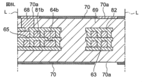
図4Aに示すようにダミーコア基板61を準備する。ダミーコア基板61の両面には基板銅箔を有する。本実施形態では、ダミーコア基板61はガラスエポキシ基板である。ダミーコア基板61の厚みは、インダクタ部品の厚みに影響を与えないため、加工上のそりなどの理由から適便取り扱いやすい厚さのものを用いればよい。
A
次に、基板銅箔の面上に銅箔62を接着する。銅箔62は基板銅箔の円滑面に接着される。このため、銅箔62と基板銅箔の接着力を弱くすることでき、後工程において、ダミーコア基板61を銅箔62から容易に剥がすことができる。好ましくはダミーコア基板61とダミー金属層(銅箔62)を接着する接着剤は、低粘着剤とする。また、ダミーコア基板61と銅箔62の接着力を弱くするために、ダミーコア基板61と銅箔62の接着面を光沢面とすることが望ましい。
Next, a
その後、銅箔62上に絶縁層63を積層する。このとき絶縁層63は、真空ラミネータやプレス機などにより、熱圧着し、熱硬化する。
After that, an insulating
図4Bに示すように、絶縁層63をレーザ加工などにより開口部63aを形成する。そして、図4Cに示すように、絶縁層63上にダミー銅64aとスパイラル配線64bを形成する。詳しくは、絶縁層63上に無電解めっきやスパッタリング、蒸着などによりSAPのための給電膜(図示せず)を形成する。給電膜の形成後、給電膜上に感光性のレジストを塗布や貼りつけ、フォトリソグラフィによって配線パターンとなる箇所に感光性レジストの開口部を形成する。その後、ダミー銅64a、スパイラル配線64bに相当するメタル配線を感光性レジスト層の開口部に形成する。メタル配線形成後、感光性レジストを薬液により剥離除去し、給電膜をエッチング除去する。その後、さらにこのメタル配線を給電部として、追加の銅電解めっきを施すことで狭スペースな配線を得る。また、SAPにより図4Bに形成された開口部63aには銅が充填される。
As shown in FIG. 4B, an
そして、図4Dに示すように、ダミー銅64a、スパイラル配線64bを絶縁層65で覆う。絶縁層65は真空ラミネータやプレス機などにより、熱圧着し、熱硬化する。
Then, as shown in FIG. 4D, the
次に、図4Eに示すように、レーザ加工などにより絶縁層65に開口部65aを形成する。
Next, as shown in FIG. 4E, an
その後、ダミーコア基板61を銅箔62から剥がす。そして、銅箔62をエッチングなどにより取り除き、ダミー銅64aをエッチングなどにより取り除いて、図4Fに示すように、内磁路部13に対応する孔部66aと外磁路部14に対応する孔部66bを形成する。
After that, the
その後、図4Gに示すように、絶縁層開口部67aをレーザ加工などにより形成する。そして、図4Hに示すように、SAPにより絶縁層開口部67aを銅により充填し、絶縁層67上に柱状配線68を形成する。
Thereafter, as shown in FIG. 4G, an insulating
次に、図4Iに示すように、磁性材料(磁性層)69によりスパイラル配線、絶縁層、柱状配線を覆って、インダクタ基板を形成する。磁性材料69は、真空ラミネータやプレス機などにより、熱圧着し、熱硬化する。このとき、磁性材料69は、孔部66a,66bにも充填される。
Next, as shown in FIG. 4I, a magnetic material (magnetic layer) 69 covers the spiral wiring, insulating layer, and columnar wiring to form an inductor substrate. The
そして、図4Jに示すように、インダクタ基板の上下の磁性材料69を研削工法により薄層化する。このとき、柱状配線68の一部を露出されることで、磁性材料69の同一平面上に柱状配線68の露出部が形成される。このとき、インダクタンス値が得られるのに十分な厚みまで磁性材料69を研削することで、インダクタ部品の薄型化を図ることができる。
Then, as shown in FIG. 4J, the
その後、図4Kに示すように、印刷工法により磁性体表面に絶縁樹脂(被覆膜)70を形成する。ここで、絶縁樹脂70の開口部70aを、外部端子の形成部分とする。本実施例では、印刷工法を用いたが、フォトリソグラフィ法によって開口部70aを形成してもよい。
After that, as shown in FIG. 4K, an insulating resin (coating film) 70 is formed on the surface of the magnetic material by a printing method. Here, the
次に、図4Lに示すように、無電解銅めっきや、NiおよびAuなどのめっき被膜し、外部端子71aを形成し、図4Mに示すように、破線部Lにてダイシングにより個片化し、図2のインダクタ部品を得る。なお、図4B以降、記載を省略したが、ダミーコア基板61の両面にインダクタ基板を形成してもよい。これにより、高い生産性を得ることができる。
Next, as shown in FIG. 4L, electroless copper plating, plating film such as Ni and Au are applied to form
なお、この実施形態では、第2磁性層12側にも外部端子を設けているが、第2磁性層12側に外部端子を設けない場合、図4Kに示すように、磁性材料69の下面に絶縁樹脂70を設けない。
In this embodiment, external terminals are also provided on the second
(第2実施形態)
図5は、インダクタ部品の断面図である。第2実施形態は、第1実施形態とは、第2磁性層の構成が相違する。この相違する構成を以下に説明する。なお、第2実施形態において、第1実施形態と同一の符号は、第1実施形態と同じ構成であるため、その説明を省略する。
(Second embodiment)
FIG. 5 is a cross-sectional view of an inductor component. The second embodiment differs from the first embodiment in the configuration of the second magnetic layer. This different configuration is described below. In addition, in 2nd Embodiment, since the code|symbol same as 1st Embodiment is the same structure as 1st Embodiment, the description is abbreviate|omitted.
図5に示すように、インダクタ部品1Aでは、第2磁性層12Aの透磁率は、第1磁性層11の透磁率よりも高い。したがって、インダクタンスの取得効率を高くできる。このとき、第1磁性層11の厚みAは、好ましくは、第2磁性層12Aの厚みBよりも厚い。これにより、第2磁性層12Aの厚みBが薄くても、第2磁性層12Aの透磁率は高くて、漏れ磁束が生じにくくなり、さらに、第1磁性層11の厚みが厚いことから、第1磁性層11側の漏れ磁束も生じにくくなる。
As shown in FIG. 5, in the
ここで、透磁率の解析方法について述べる。透磁率の大小は、以下の第1、第2または第3の解析方法により、評価することができる。基本、第1または第2の解析方法を用いて測定するが、第1または第2の解析方法を用いることができないときにのみ、第3の解析方法を用いて測定する。 Here, a method of analyzing magnetic permeability will be described. The magnitude of magnetic permeability can be evaluated by the following first, second, or third analysis methods. Measurement is performed using the basic, first or second analysis method, and the third analysis method is used only when the first or second analysis method cannot be used.
第1の解析方法としては、磁性材料を液状、シート状などで入手できる場合はそれらをシート、板、ブロック状に加工し、公知のインピーダンス測定方法により透磁率を取得できることができる。 As a first analysis method, if the magnetic material is available in the form of a liquid or a sheet, it can be processed into a sheet, plate, or block, and the magnetic permeability can be obtained by a known impedance measurement method.
第2の解析方法としては、チップ状態からは、例えば、チップのインダクタンスを測定した後、磁性層の一面を研削やエッチングなどにより除去し、再度インダクタンスを測定する。その後、電磁界シミュレーション(例えばアンシス社のHFSS)でそれぞれの状態に対応するインダクタンスとなる実行透磁率を求めることで、チップ状態からの透磁率を比較することが可能である。 As a second analysis method, after measuring the inductance of the chip, for example, one surface of the magnetic layer is removed by grinding or etching, and the inductance is measured again. After that, it is possible to compare the magnetic permeability from the chip state by obtaining the effective magnetic permeability, which is the inductance corresponding to each state, by an electromagnetic field simulation (for example, HFSS of ANSYS).
第3の解析方法としては、一般的な、公知の知識よりSEM画像の断面から判断することができる。例えば、EDX分析の結果から、同じ材料系の磁性粉が使用されていれば、粒径が大きい磁性粉が多い、磁性材料の方が、少ない磁性材料よりも透磁率は高い。ここで、取得するSEM画像はチップの長手側の中心をカットして得られる断面から得て良い。また、SEM画像の倍率は200~2000倍であることが好ましい。 As a third analysis method, determination can be made from the cross section of the SEM image based on general and publicly known knowledge. For example, from the results of EDX analysis, if magnetic powders of the same material system are used, a magnetic material with more magnetic powder having a larger particle size has a higher magnetic permeability than a magnetic material with less magnetic powder. Here, the SEM image to be acquired may be obtained from a cross section obtained by cutting the center of the chip on the long side. Also, the magnification of the SEM image is preferably 200 to 2000 times.
また、垂直配線51,52は、第2磁性層12Aの内部には存在しない。この場合、透磁率が第1磁性層11よりも高い第2磁性層12Aにおいて、磁性材の体積が減る垂直配線を形成しないことで、インダクタンスの取得効率が上がる。また、第2磁性層12Aは第1磁性層11よりも透磁率が高いため、磁性層中の磁性材料の割合(体積)が大きく、加工によって磁性材料の脱粒や欠損が発生しやすく、かつ脱硫や欠損のインダクタンスへの影響も大きい。すなわち、第2磁性層12Aは第1磁性層11よりも加工による影響が大きいため、第2磁性層12Aの内部に垂直配線を形成しないことで、歩留まりを高くできる。
Also, the
また、第1磁性層11は、好ましくは、FeSi系もしくはFeCo系もしくはFeAl系合金もしくはそれらのアモルファス合金からなる無機フィラーと、エポキシもしくはポリイミドもしくはフェノール系の有機樹脂とのコンポジット材料であり、無機フィラーの含有率は、好ましくは、有機樹脂に対して50vol%以上あり、無機フィラーは、好ましくは、略球形である。
The first
したがって、第1磁性層11は、無機フィラーと有機樹脂のコンポジット材料であり、無機フィラーの含有率は、50vol%以上あるので、第1磁性層11に垂直配線51,52を設けても、磁気特性と加工性を両立できる。また、無機フィラーは、略球形であるので、第1磁性層11に垂直配線51,52を設けるとき、垂直配線51,52が滑って第1磁性層11に充填されやすくなる。
Therefore, the first
図6は、インダクタ部品1Aの拡大図である。図6に示すように、第1磁性層11と第2磁性層12Aとの間の少なくとも一部において、第1磁性層11および第2磁性層12Aと比較して磁性粉(無機フィラー)101,102の量が少ない領域が存在する。この領域は、第1磁性層11に含まれる樹脂成分および第2磁性層12Aに含まれる樹脂成分で構成されてよく、あるいは、第1磁性層11および第2磁性層12Aに含まれる樹脂成分とは異なる樹脂で構成されてもよい。以下、この領域を樹脂層16とよぶ。
FIG. 6 is an enlarged view of the
樹脂層16は、磁性粉を含まないものであり得るが、第1磁性層11および第2磁性層12Aよりも磁性粉の存在量が少ない限りにおいて、磁性粉を含有してもよい。樹脂層16に含まれる磁性粉は、第1、第2磁性層11,12Aに含まれる磁性粉と同じであってよい。
The
したがって、第1磁性層11と第2磁性層12Aとの間に樹脂層16が存在するので、第1磁性層11と第2磁性層12Aとの間の密着性が向上し、インダクタ部品1Aの磁性層10の強度を向上させることができる。また、磁性粉の少ない樹脂層16を設けることで、磁気飽和特性が向上し得る。
Therefore, since the
樹脂層16の厚さが大きいほど、密着性および磁気飽和特性が向上するが、樹脂層16の厚さが大きすぎると、インダクタンスの取得効率が低下するおそれがある。樹脂層16の厚さは、0.5μm以上30μm以下であることが好ましい。樹脂層16の厚さが0.5μm以上であると、第1磁性層11と第2磁性層12Aとの間の密着性をより一層向上させることができ、かつ、磁気飽和特性をより一層向上させることができる。樹脂層16の厚さが30μm以下であると、密着性および磁気飽和特性が向上すると同時に、インダクタンスの取得効率の低下を抑制することができる。
As the thickness of the
また、第1磁性層11は、略球形の磁性粉101を含み、第2磁性層12Aは、偏平形の磁性粉102を含む。第2磁性層12Aにおいて、偏平形の磁性粉101は、その長軸が法線方向(Z方向)と直交する方向に沿って配列される。これにより、第2磁性層12Aにおいて、磁束は、法線方向(Z方向)と直交する方向に沿って流れる。したがって、第2磁性層12Aは、第1磁性層11と比べて、透磁率が高くなる。
The first
なお、第1と第2磁性層11,12Aには、異種材料、または、高充填化した材料を使用してもよい。または、第1と第2磁性層11,12Aにおいて磁性粉の充填量に勾配をかけて、第1磁性層11よりも第2磁性層12Aの実効透磁率を高くしてもよい。
Note that different materials or highly filled materials may be used for the first and second
(第3実施形態)
(構成)
図7Aは、インダクタ部品の第3実施形態を示す透視平面図である。図7Bは、図7AのX-X断面図である。第3実施形態は、第1実施形態とは、スパイラル配線の構成が相違する。この相違する構成を以下に説明する。なお、第3実施形態において、第1実施形態と同一の符号は、第1実施形態と同じ構成であるため、その説明を省略する。
(Third embodiment)
(composition)
FIG. 7A is a perspective plan view showing a third embodiment of an inductor component; FIG. FIG. 7B is a cross-sectional view taken along line XX of FIG. 7A. The third embodiment differs from the first embodiment in the configuration of the spiral wiring. This different configuration is described below. In addition, in 3rd Embodiment, since the code|symbol same as 1st Embodiment is the same structure as 1st Embodiment, the description is abbreviate|omitted.
図7Aと図7Bに示すように、インダクタ部品1Bは、インダクタ部品1と同様に、スパイラル配線21,22からZ方向に延伸し、第1磁性層11または第2磁性層12の内部を貫通する垂直配線51~53を備える。
As shown in FIGS. 7A and 7B,
一方、インダクタ部品1Bでは、スパイラル配線は第1スパイラル配線21と第2スパイラル配線22の複数あり、第1スパイラル配線21と第2スパイラル配線22との間を直列に接続する第2ビア導体27をさらに備える。具体的に述べると、第1スパイラル配線21と第2スパイラル配線22は、Z方向に積層されている。第1スパイラル配線21は、上側からみて、外周端21bから内周端21aに向かって反時計回り方向に渦巻状に巻回されている。第2スパイラル配線22は、上側からみて、内周端22aから外周端22bに向かって反時計回り方向に渦巻状に巻回されている。
On the other hand, in
第1スパイラル配線21の外周端21bは、その外周端21bの上側の第1垂直配線51(ビア導体25および第1柱状配線31)を介して、第1外部端子41に接続される。第1スパイラル配線21の内周端21aは、その内周端21aの下側の第2ビア導体27を介して、第2スパイラル配線22の内周端22aに接続される。
The outer
第2スパイラル配線22の外周端22bは、その外周端22bの上側の第2垂直配線52(ビア導体25、26および第2柱状配線32)を介して、第2外部端子42に接続される。第2スパイラル配線22の外周端22bは、その外周端22bの下側の第3垂直配線53(ビア導体25および第3柱状配線33)を介して、第3外部端子43に接続される。ビア導体26は、第2スパイラル配線22の外周端22bの上側のビア導体25からZ方向に延在し絶縁層15の内部を貫通する。ビア導体26は、第1スパイラル配線21と同一平面上に形成される。
The outer
第2ビア導体27を含む第2ビア導体27と同一層は、導体、無機フィラーおよび有機樹脂のみを含む。つまり、同一層は、第2ビア導体27、絶縁層15および磁性層10のみを含む。したがって、第2ビア導体27と同一層は、ある程度の厚みが必要なガラスクロスなどの基材を含まないので、薄型化を可能にしつつ、電気的特性に寄与しない部分が相対的に減少することで、同じ厚みであっても電気的特性を向上させることができる。なお、「第2ビア導体27と同一層」とは、法線方向(Z方向)について、第2ビア導体27の上端から下端までの領域と同じ位置にある部分(層)を指す。言い換えると、スパイラル配線21が巻回された平面と平行な面について、第2ビア導体27の上端から下端までの領域と同一面にある部分(層)を指す。
これに対して、従来のインダクタ部品は、非磁性のプリント基板を有しており、このプリント基板の厚みは、60μmと厚いために、チップ厚が薄くなるにつれて、チップ全体の非磁性領域が占める割合が増加してくる。この結果、チップ厚が薄くなるほど、インダクタンスの取得効率の低下が大きくなる。 また、パワーインダクタの重要な特性指標として、直流抵抗Rdcがあるが、直流抵抗Rdcを維持したまま、チップ厚を薄くしようとすると、スパイラル配線の厚みを維持しつつ、チップ厚を薄くする必要があるため、その結果、磁性層の厚みが薄くなり、インダクタンスの取得効率の低下や磁束漏れが発生する可能性がある。例えば、ランドパターン側に磁束がもれると、ランドパターンの導体内で渦電流が発生し、発生した渦電流により、磁束を打ち消す方向に新たな磁束が生成される。その結果、インダクタンスが低下することになる。また、漏れ磁束による磁気ノイズの伝播により周りの電子部品へ影響を及ぼすことが懸念される。
The same layer as the second via
On the other hand, the conventional inductor component has a non-magnetic printed circuit board, and the thickness of this printed circuit board is as thick as 60 μm. percentage will increase. As a result, the smaller the chip thickness, the greater the drop in inductance acquisition efficiency. In addition, DC resistance Rdc is an important characteristic index of power inductors. If the chip thickness is to be reduced while maintaining the DC resistance Rdc, it is necessary to reduce the chip thickness while maintaining the thickness of the spiral wiring. Therefore, as a result, the thickness of the magnetic layer is reduced, and there is a possibility that the inductance acquisition efficiency is lowered and magnetic flux leakage occurs. For example, when magnetic flux leaks to the land pattern side, an eddy current is generated in the conductor of the land pattern, and the generated eddy current generates a new magnetic flux in the direction of canceling the magnetic flux. As a result, the inductance will decrease. In addition, there is concern that the magnetic noise propagated by the leaked magnetic flux may affect surrounding electronic components.
第2ビア導体27と同一層の厚みは、好ましくは、1μm以上でかつ20μm以下である。したがって、第2ビア導体27と同一層の厚みは、1μm以上であるので、スパイラル配線間のショートを確実に防ぐことができ、第2ビア導体27と同一層の厚みは、20μm以下であるので、薄型のインダクタ部品1Bを提供できる。
The thickness of the same layer as second via
無機フィラーは、好ましくは、FeSi系合金、FeCo合金、FeAl合金、それらのアモルファス合金およびSiO2のうちの少なくとも一つからなり、無機フィラーの平均粒径は、好ましくは、5μm以下である。したがって、高周波での損失の低減や、絶縁性の確保を図ることができる。 The inorganic filler preferably consists of at least one of FeSi-based alloys, FeCo alloys, FeAl alloys, amorphous alloys thereof and SiO2 , and the average particle size of the inorganic filler is preferably 5 μm or less. Therefore, it is possible to reduce loss at high frequencies and ensure insulation.
また、インダクタ部品1Bでは、第2ビア導体27により、第1スパイラル配線21と第2スパイラル配線22とが直列に接続されているので、ターン数を増やすことでインダクタンス値を向上できる。また、第1から第3垂直配線51~53を第1、第2スパイラル配線21,22の外周から出すことができるので、第1、第2スパイラル配線21,22の内径を大きくとることができ、インダクタンス値を向上できる。
In addition, in
また、第1スパイラル配線21と第2スパイラル配線22は、それぞれ法線方向に積層されているので、ターン数に対してZ方向からみたインダクタ部品1Bの面積、すなわち実装面積を低減でき、インダクタ部品1Bの小型化が実現できる。
In addition, since the
なお、インダクタ部品1Bでは、直列接続されたスパイラル配線を偶数備える構成であったが、これに限られず、直列接続されたスパイラル配線は奇数であってもよい。垂直配線は、スパイラル配線からZ方向に配線を引き出すため、直列接続されたスパイラル配線が奇数個であって、インダクタの一方の端部が内周側に配置されていても、該端部を外周側に引き出す必要がない。したがって、この場合、薄型化を実現することができる。また、このように、直列接続されるスパイラル配線の数の自由度が向上するため、インダクタンス値の設定範囲の自由度も向上する。
Although the
また、インダクタ部品1Bでは、2層のスパイラル配線からなるインダクタを同一平面上に1つ配置しているが、同一平面上にインダクタを2つ以上配置していてもよい。
Further, in the
(製造方法)
次に、インダクタ部品1Bの製造方法について説明する。
(Production method)
Next, a method for manufacturing
まず、インダクタ部品1の製造方法の図4Aから図4Cに示す工程を行う。続いて、図8Aに示すように、第1のダミー銅64aおよび第1のスパイラル配線64bを第1の絶縁層65で覆う。絶縁層65は、真空ラミネータやプレス機などにより、熱圧着し、熱硬化する。
First, the steps shown in FIGS. 4A to 4C of the manufacturing method of the
そして、図8Bに示すように、レーザ加工などにより、ダミー銅64a上の絶縁層65を開口して開口部65aを形成し、スパイラル配線64bの端部上の絶縁層65を開口して開口部65bを形成する。
Then, as shown in FIG. 8B, by laser processing or the like, the insulating
次に、図8Cに示すように、図8Cと同じようにSAPとその後の追加銅電極めっきを行って、第2のダミー銅81aと第2のスパイラル配線81bを形成する。なお、スパイラル配線の積層数を増やす場合、図8Aから図8Cを繰り返せばよい。
Next, as shown in FIG. 8C, SAP and subsequent additional copper electrode plating are performed in the same manner as in FIG. 8C to form
そして、図8Dに示すように、第2のダミー銅81aおよび第2のスパイラル配線81bを第2の絶縁層82で覆う。絶縁層82は、真空ラミネータやプレス機などにより、熱圧着し、熱硬化する。そして、レーザ加工などにより、第2のダミー銅81a上の絶縁層82の開口部82aを形成する。
Then, as shown in FIG. 8D, the
その後、ダミーコア基板61を銅箔62から剥がす。そして、銅箔62をエッチングなどにより取り除き、ダミー銅64aをエッチングなどにより取り除いて、図8Eに示すように、内磁路に対応する孔部66aと外磁路に対応する孔部66bを形成する。
After that, the
その後、図8Fに示すように、絶縁層82に開口部87aをレーザ加工などにより形成する。そして、図8Gに示すように、SAPにより絶縁層82の開口部87aを銅により充填し、絶縁層82上に柱状配線68を形成する。
After that, as shown in FIG. 8F, an
次に、図8Hに示すように、磁性材料(磁性層)69によりスパイラル配線、絶縁層、柱状配線を覆って、インダクタ基板を形成する。磁性材料69は、真空ラミネータやプレス機などにより、熱圧着し、熱硬化する。このとき、磁性材料69は、孔部66a,66bにも充填される。
Next, as shown in FIG. 8H, a magnetic material (magnetic layer) 69 covers the spiral wiring, insulating layer, and columnar wiring to form an inductor substrate. The
そして、図8Iに示すように、インダクタ基板の上下の磁性材料69を研削工法により薄層化する。このとき、柱状配線68の一部を露出されることで、磁性材料69の同一平面上に柱状配線68の露出部が形成される。
Then, as shown in FIG. 8I, the
その後、図8Jに示すように、印刷工法により磁性体表面に絶縁樹脂(絶縁層)70を形成する。ここで、絶縁樹脂70の開口部70aを、外部端子の形成部分とする。上記では、印刷工法を用いたが、フォトリソグラフィ法によって開口部70aを形成してもよい。
After that, as shown in FIG. 8J, an insulating resin (insulating layer) 70 is formed on the surface of the magnetic material by a printing method. Here, the
次に、図8Kに示すように、無電解銅めっきや、NiおよびAuなどのめっき被膜し、外部端子71aを形成し、図8Lに示すように、破線部Lにてダイシングにより個片化し、図7のインダクタ部品1Bを得る。なお、ダミーコア基板61の両面にインダクタ基板を形成してもよい。これにより、高い生産性を得ることができる。
Next, as shown in FIG. 8K, electroless copper plating, Ni and Au plating films are applied to form
なお、本開示は上述の実施形態に限定されず、本開示の要旨を逸脱しない範囲で設計変更可能である。例えば、第1から第3実施形態のそれぞれの特徴点を様々に組み合わせてもよい。 Note that the present disclosure is not limited to the above-described embodiments, and design changes are possible without departing from the gist of the present disclosure. For example, each characteristic point of the first to third embodiments may be combined in various ways.
また、第1から第3実施形態において、他の実施形態で説明した作用効果であって、該実施形態では特に言及せず、説明を省略しているものであっても、該実施形態で同様の構成を有する場合は、該実施形態においても基本的に同じ作用効果は発揮される。 Also, in the first to third embodiments, even if there are functions and effects described in other embodiments that are not specifically mentioned in the embodiments and the description is omitted, the same applies to the embodiments. In the case of having the configuration of , basically the same effects are exhibited in this embodiment as well.
1,1A,1B インダクタ部品
10 磁性層
11 第1磁性層
12,12A 第2磁性層
13 内磁路部
14 外磁路部
15 絶縁層
16 樹脂層(磁性粉の量の少ない領域)
21 第1スパイラル配線
22 第2スパイラル配線
25 ビア導体
31 第1柱状配線
32 第2柱状配線
33 第3柱状配線
41 第1外部端子
42 第2外部端子
43 第3外部端子
50 被覆膜
51 第1垂直配線
52 第2垂直配線
53 第3垂直配線
21
Claims (15)
前記スパイラル配線が巻回された平面に対する法線方向の両側から前記スパイラル配線を挟む位置にある第1磁性層および第2磁性層と、
前記スパイラル配線から前記法線方向に延在し、前記第1磁性層および前記第2磁性層の内部を貫通する垂直配線と、
前記第1磁性層の表面および前記第2磁性層の表面に設けられ、前記垂直配線の端面を覆う外部端子と
を備え、
前記法線方向からみた前記外部端子の面積に関して、前記第1磁性層は、前記第2磁性層よりも大きく、
前記第1磁性層の厚みは、前記第2磁性層の厚みよりも厚く、
前記第1磁性層の厚みをAとし、前記第2磁性層の厚みをBとしたとき、A/((A+B)/2)が1.0より大きくかつ1.6以下となり、
前記第2磁性層の透磁率は、前記第1磁性層の透磁率よりも高い、インダクタ部品。 spiral wiring wound on a plane;
a first magnetic layer and a second magnetic layer located at positions sandwiching the spiral wire from both sides in the direction normal to the plane on which the spiral wire is wound;
a vertical wire extending from the spiral wire in the normal direction and penetrating through the insides of the first magnetic layer and the second magnetic layer;
an external terminal provided on the surface of the first magnetic layer and the surface of the second magnetic layer and covering an end surface of the vertical wiring;
With respect to the area of the external terminal viewed from the normal direction, the first magnetic layer is larger than the second magnetic layer,
The thickness of the first magnetic layer is thicker than the thickness of the second magnetic layer,
where A is the thickness of the first magnetic layer and B is the thickness of the second magnetic layer, A/((A+B)/2) is greater than 1.0 and less than or equal to 1.6 ;
The inductor component , wherein the magnetic permeability of the second magnetic layer is higher than the magnetic permeability of the first magnetic layer .
前記スパイラル配線が巻回された平面に対する法線方向の両側から前記スパイラル配線を挟む位置にある第1磁性層および第2磁性層と、
前記スパイラル配線から前記法線方向に延在し、前記第1磁性層および前記第2磁性層の内の少なくとも前記第1磁性層の内部を貫通する垂直配線と、
前記第1磁性層および前記第2磁性層の内の少なくとも前記第1磁性層の表面に設けられ、前記垂直配線の端面を覆う外部端子と
を備え、
前記法線方向からみた前記外部端子の面積に関して、前記第1磁性層は、前記第2磁性層よりも大きく、
前記第1磁性層の厚みは、前記第2磁性層の厚みよりも厚く、
前記第1磁性層の厚みをAとし、前記第2磁性層の厚みをBとしたとき、A/((A+B)/2)が1.0より大きくかつ1.3以下となり、
前記第2磁性層の透磁率は、前記第1磁性層の透磁率よりも高い、インダクタ部品。 spiral wiring wound on a plane;
a first magnetic layer and a second magnetic layer located at positions sandwiching the spiral wire from both sides in the direction normal to the plane on which the spiral wire is wound;
a vertical wire extending from the spiral wire in the normal direction and penetrating through at least the first magnetic layer of the first magnetic layer and the second magnetic layer;
an external terminal provided on the surface of at least the first magnetic layer of the first magnetic layer and the second magnetic layer and covering an end surface of the vertical wiring;
With respect to the area of the external terminal viewed from the normal direction, the first magnetic layer is larger than the second magnetic layer,
The thickness of the first magnetic layer is thicker than the thickness of the second magnetic layer,
where A is the thickness of the first magnetic layer and B is the thickness of the second magnetic layer, A/((A+B)/2) is greater than 1.0 and less than or equal to 1.3 ;
The inductor component , wherein the magnetic permeability of the second magnetic layer is higher than the magnetic permeability of the first magnetic layer .
前記無機フィラーの含有率は、前記有機樹脂に対して50vol%以上あり、前記無機フィラーは、略球形である、請求項9に記載のインダクタ部品。 The first magnetic layer is a composite material of an inorganic filler made of FeSi-based, FeCo-based, FeAl-based alloys, or amorphous alloys thereof, and an epoxy, polyimide, or phenol-based organic resin,
10. The inductor component according to claim 9 , wherein a content of said inorganic filler is 50 vol % or more with respect to said organic resin, and said inorganic filler has a substantially spherical shape.
前記複数個のスパイラル配線間において、前記スパイラル配線同士を直列に接続するビア導体をさらに備え、
前記ビア導体を含む前記ビア導体と同一層は、導体、無機フィラーおよび有機樹脂のみを含む、請求項1または2に記載のインダクタ部品。 there are a plurality of the spiral wirings,
further comprising a via conductor connecting the spiral wires in series between the plurality of spiral wires;
3. The inductor component according to claim 1, wherein the same layer as said via conductors containing said via conductors contains only a conductor, an inorganic filler and an organic resin.
Priority Applications (2)
| Application Number | Priority Date | Filing Date | Title |
|---|---|---|---|
| JP2020140164A JP7253520B2 (en) | 2020-08-21 | 2020-08-21 | inductor components |
| JP2022005757A JP7414082B2 (en) | 2020-08-21 | 2022-01-18 | inductor parts |
Applications Claiming Priority (1)
| Application Number | Priority Date | Filing Date | Title |
|---|---|---|---|
| JP2020140164A JP7253520B2 (en) | 2020-08-21 | 2020-08-21 | inductor components |
Related Parent Applications (1)
| Application Number | Title | Priority Date | Filing Date |
|---|---|---|---|
| JP2017169437A Division JP6912976B2 (en) | 2017-09-04 | 2017-09-04 | Inductor parts |
Related Child Applications (1)
| Application Number | Title | Priority Date | Filing Date |
|---|---|---|---|
| JP2022005757A Division JP7414082B2 (en) | 2020-08-21 | 2022-01-18 | inductor parts |
Publications (2)
| Publication Number | Publication Date |
|---|---|
| JP2020191476A JP2020191476A (en) | 2020-11-26 |
| JP7253520B2 true JP7253520B2 (en) | 2023-04-06 |
Family
ID=73453937
Family Applications (2)
| Application Number | Title | Priority Date | Filing Date |
|---|---|---|---|
| JP2020140164A Active JP7253520B2 (en) | 2020-08-21 | 2020-08-21 | inductor components |
| JP2022005757A Active JP7414082B2 (en) | 2020-08-21 | 2022-01-18 | inductor parts |
Family Applications After (1)
| Application Number | Title | Priority Date | Filing Date |
|---|---|---|---|
| JP2022005757A Active JP7414082B2 (en) | 2020-08-21 | 2022-01-18 | inductor parts |
Country Status (1)
| Country | Link |
|---|---|
| JP (2) | JP7253520B2 (en) |
Citations (5)
| Publication number | Priority date | Publication date | Assignee | Title |
|---|---|---|---|---|
| JP2004014837A (en) | 2002-06-07 | 2004-01-15 | Jfe Steel Kk | Plane magnetic element |
| JP2008085057A (en) | 2006-09-27 | 2008-04-10 | Nitta Ind Corp | Electromagnetic wave absorbing material |
| JP2014127717A (en) | 2012-12-26 | 2014-07-07 | Samsung Electro-Mechanics Co Ltd | Common mode filter and method of manufacturing the same |
| JP2017069523A (en) | 2015-10-02 | 2017-04-06 | 株式会社村田製作所 | Inductor component, package component and switching regulator |
| JP2017103355A (en) | 2015-12-02 | 2017-06-08 | Tdk株式会社 | Manufacturing method of coil component, coil component, and power supply circuit unit |
Family Cites Families (4)
| Publication number | Priority date | Publication date | Assignee | Title |
|---|---|---|---|---|
| JP2006210541A (en) * | 2005-01-27 | 2006-08-10 | Nec Tokin Corp | Inductor |
| JP2010205905A (en) * | 2009-03-03 | 2010-09-16 | Fuji Electric Systems Co Ltd | Magnetic component, and method of manufacturing the magnetic component |
| WO2016013643A1 (en) * | 2014-07-25 | 2016-01-28 | 株式会社村田製作所 | Electronic component and method for producing same |
| JP6668723B2 (en) * | 2015-12-09 | 2020-03-18 | 株式会社村田製作所 | Inductor components |
-
2020
- 2020-08-21 JP JP2020140164A patent/JP7253520B2/en active Active
-
2022
- 2022-01-18 JP JP2022005757A patent/JP7414082B2/en active Active
Patent Citations (5)
| Publication number | Priority date | Publication date | Assignee | Title |
|---|---|---|---|---|
| JP2004014837A (en) | 2002-06-07 | 2004-01-15 | Jfe Steel Kk | Plane magnetic element |
| JP2008085057A (en) | 2006-09-27 | 2008-04-10 | Nitta Ind Corp | Electromagnetic wave absorbing material |
| JP2014127717A (en) | 2012-12-26 | 2014-07-07 | Samsung Electro-Mechanics Co Ltd | Common mode filter and method of manufacturing the same |
| JP2017069523A (en) | 2015-10-02 | 2017-04-06 | 株式会社村田製作所 | Inductor component, package component and switching regulator |
| JP2017103355A (en) | 2015-12-02 | 2017-06-08 | Tdk株式会社 | Manufacturing method of coil component, coil component, and power supply circuit unit |
Also Published As
| Publication number | Publication date |
|---|---|
| JP2022050651A (en) | 2022-03-30 |
| JP2020191476A (en) | 2020-11-26 |
| JP7414082B2 (en) | 2024-01-16 |
Similar Documents
| Publication | Publication Date | Title |
|---|---|---|
| CN114156045B (en) | Inductor component | |
| US12087502B2 (en) | Inductor component | |
| US10784039B2 (en) | Inductor component and inductor-component incorporating substrate | |
| US11735353B2 (en) | Inductor component and method of manufacturing same | |
| JP7156209B2 (en) | Inductor components and substrates with built-in inductor components | |
| US12057258B2 (en) | Inductor array component and inductor array component built-in substrate | |
| CN112562966A (en) | Inductance component | |
| US11908606B2 (en) | Inductor array component | |
| US11587721B2 (en) | Inductor component and substrate with built-in inductor component | |
| JP7253520B2 (en) | inductor components | |
| CN112652445B (en) | Inductor component | |
| JP7411590B2 (en) | Inductor parts and their manufacturing method |
Legal Events
| Date | Code | Title | Description |
|---|---|---|---|
| A621 | Written request for application examination |
Free format text: JAPANESE INTERMEDIATE CODE: A621 Effective date: 20200824 |
|
| A131 | Notification of reasons for refusal |
Free format text: JAPANESE INTERMEDIATE CODE: A131 Effective date: 20210622 |
|
| A521 | Request for written amendment filed |
Free format text: JAPANESE INTERMEDIATE CODE: A523 Effective date: 20210803 |
|
| A02 | Decision of refusal |
Free format text: JAPANESE INTERMEDIATE CODE: A02 Effective date: 20211026 |
|
| C60 | Trial request (containing other claim documents, opposition documents) |
Free format text: JAPANESE INTERMEDIATE CODE: C60 Effective date: 20220118 |
|
| C22 | Notice of designation (change) of administrative judge |
Free format text: JAPANESE INTERMEDIATE CODE: C22 Effective date: 20221011 |
|
| C13 | Notice of reasons for refusal |
Free format text: JAPANESE INTERMEDIATE CODE: C13 Effective date: 20221101 |
|
| A521 | Request for written amendment filed |
Free format text: JAPANESE INTERMEDIATE CODE: A523 Effective date: 20221227 |
|
| C23 | Notice of termination of proceedings |
Free format text: JAPANESE INTERMEDIATE CODE: C23 Effective date: 20230221 |
|
| C03 | Trial/appeal decision taken |
Free format text: JAPANESE INTERMEDIATE CODE: C03 Effective date: 20230322 |
|
| C30A | Notification sent |
Free format text: JAPANESE INTERMEDIATE CODE: C3012 Effective date: 20230322 |
|
| A61 | First payment of annual fees (during grant procedure) |
Free format text: JAPANESE INTERMEDIATE CODE: A61 Effective date: 20230327 |
|
| R150 | Certificate of patent or registration of utility model |
Ref document number: 7253520 Country of ref document: JP Free format text: JAPANESE INTERMEDIATE CODE: R150 |