JP7246863B2 - Photodetector, vehicle control system and rangefinder - Google Patents
Photodetector, vehicle control system and rangefinder Download PDFInfo
- Publication number
- JP7246863B2 JP7246863B2 JP2018081068A JP2018081068A JP7246863B2 JP 7246863 B2 JP7246863 B2 JP 7246863B2 JP 2018081068 A JP2018081068 A JP 2018081068A JP 2018081068 A JP2018081068 A JP 2018081068A JP 7246863 B2 JP7246863 B2 JP 7246863B2
- Authority
- JP
- Japan
- Prior art keywords
- pixel
- light
- sensitivity
- pixels
- light receiving
- Prior art date
- Legal status (The legal status is an assumption and is not a legal conclusion. Google has not performed a legal analysis and makes no representation as to the accuracy of the status listed.)
- Active
Links
- 230000035945 sensitivity Effects 0.000 claims description 88
- 238000001514 detection method Methods 0.000 claims description 54
- 239000004065 semiconductor Substances 0.000 claims description 15
- 230000004044 response Effects 0.000 claims description 11
- 238000004891 communication Methods 0.000 description 45
- 238000003384 imaging method Methods 0.000 description 27
- 238000010586 diagram Methods 0.000 description 19
- 238000012545 processing Methods 0.000 description 18
- 230000006870 function Effects 0.000 description 13
- 230000003287 optical effect Effects 0.000 description 13
- 238000005516 engineering process Methods 0.000 description 12
- 230000015556 catabolic process Effects 0.000 description 6
- 238000009792 diffusion process Methods 0.000 description 5
- 238000005259 measurement Methods 0.000 description 5
- 230000007246 mechanism Effects 0.000 description 4
- 238000002360 preparation method Methods 0.000 description 4
- 230000003247 decreasing effect Effects 0.000 description 3
- 230000000694 effects Effects 0.000 description 3
- 230000033001 locomotion Effects 0.000 description 3
- 238000000034 method Methods 0.000 description 3
- 240000004050 Pentaglottis sempervirens Species 0.000 description 2
- 235000004522 Pentaglottis sempervirens Nutrition 0.000 description 2
- 230000001133 acceleration Effects 0.000 description 2
- 230000010267 cellular communication Effects 0.000 description 2
- 238000006243 chemical reaction Methods 0.000 description 2
- 238000002485 combustion reaction Methods 0.000 description 2
- 238000009434 installation Methods 0.000 description 2
- 238000000691 measurement method Methods 0.000 description 2
- 229920006395 saturated elastomer Polymers 0.000 description 2
- 230000005236 sound signal Effects 0.000 description 2
- 239000000758 substrate Substances 0.000 description 2
- 230000002730 additional effect Effects 0.000 description 1
- 230000003190 augmentative effect Effects 0.000 description 1
- 230000033228 biological regulation Effects 0.000 description 1
- 230000005540 biological transmission Effects 0.000 description 1
- 238000010276 construction Methods 0.000 description 1
- 238000001816 cooling Methods 0.000 description 1
- 238000012937 correction Methods 0.000 description 1
- 230000007423 decrease Effects 0.000 description 1
- 238000011156 evaluation Methods 0.000 description 1
- 230000001678 irradiating effect Effects 0.000 description 1
- 230000007774 longterm Effects 0.000 description 1
- 238000012423 maintenance Methods 0.000 description 1
- 239000011159 matrix material Substances 0.000 description 1
- 230000000116 mitigating effect Effects 0.000 description 1
- 238000010295 mobile communication Methods 0.000 description 1
- 238000012986 modification Methods 0.000 description 1
- 230000004048 modification Effects 0.000 description 1
- 230000008569 process Effects 0.000 description 1
- 238000010791 quenching Methods 0.000 description 1
- 230000000171 quenching effect Effects 0.000 description 1
- 238000002366 time-of-flight method Methods 0.000 description 1
Images


Classifications
-
- G—PHYSICS
- G01—MEASURING; TESTING
- G01S—RADIO DIRECTION-FINDING; RADIO NAVIGATION; DETERMINING DISTANCE OR VELOCITY BY USE OF RADIO WAVES; LOCATING OR PRESENCE-DETECTING BY USE OF THE REFLECTION OR RERADIATION OF RADIO WAVES; ANALOGOUS ARRANGEMENTS USING OTHER WAVES
- G01S7/00—Details of systems according to groups G01S13/00, G01S15/00, G01S17/00
- G01S7/48—Details of systems according to groups G01S13/00, G01S15/00, G01S17/00 of systems according to group G01S17/00
- G01S7/483—Details of pulse systems
- G01S7/486—Receivers
- G01S7/4861—Circuits for detection, sampling, integration or read-out
- G01S7/4863—Detector arrays, e.g. charge-transfer gates
-
- G—PHYSICS
- G01—MEASURING; TESTING
- G01S—RADIO DIRECTION-FINDING; RADIO NAVIGATION; DETERMINING DISTANCE OR VELOCITY BY USE OF RADIO WAVES; LOCATING OR PRESENCE-DETECTING BY USE OF THE REFLECTION OR RERADIATION OF RADIO WAVES; ANALOGOUS ARRANGEMENTS USING OTHER WAVES
- G01S7/00—Details of systems according to groups G01S13/00, G01S15/00, G01S17/00
- G01S7/48—Details of systems according to groups G01S13/00, G01S15/00, G01S17/00 of systems according to group G01S17/00
- G01S7/491—Details of non-pulse systems
- G01S7/4912—Receivers
- G01S7/4913—Circuits for detection, sampling, integration or read-out
- G01S7/4914—Circuits for detection, sampling, integration or read-out of detector arrays, e.g. charge-transfer gates
-
- G—PHYSICS
- G01—MEASURING; TESTING
- G01S—RADIO DIRECTION-FINDING; RADIO NAVIGATION; DETERMINING DISTANCE OR VELOCITY BY USE OF RADIO WAVES; LOCATING OR PRESENCE-DETECTING BY USE OF THE REFLECTION OR RERADIATION OF RADIO WAVES; ANALOGOUS ARRANGEMENTS USING OTHER WAVES
- G01S17/00—Systems using the reflection or reradiation of electromagnetic waves other than radio waves, e.g. lidar systems
- G01S17/02—Systems using the reflection of electromagnetic waves other than radio waves
- G01S17/06—Systems determining position data of a target
- G01S17/08—Systems determining position data of a target for measuring distance only
- G01S17/10—Systems determining position data of a target for measuring distance only using transmission of interrupted, pulse-modulated waves
-
- G—PHYSICS
- G01—MEASURING; TESTING
- G01S—RADIO DIRECTION-FINDING; RADIO NAVIGATION; DETERMINING DISTANCE OR VELOCITY BY USE OF RADIO WAVES; LOCATING OR PRESENCE-DETECTING BY USE OF THE REFLECTION OR RERADIATION OF RADIO WAVES; ANALOGOUS ARRANGEMENTS USING OTHER WAVES
- G01S17/00—Systems using the reflection or reradiation of electromagnetic waves other than radio waves, e.g. lidar systems
- G01S17/88—Lidar systems specially adapted for specific applications
-
- G—PHYSICS
- G01—MEASURING; TESTING
- G01S—RADIO DIRECTION-FINDING; RADIO NAVIGATION; DETERMINING DISTANCE OR VELOCITY BY USE OF RADIO WAVES; LOCATING OR PRESENCE-DETECTING BY USE OF THE REFLECTION OR RERADIATION OF RADIO WAVES; ANALOGOUS ARRANGEMENTS USING OTHER WAVES
- G01S7/00—Details of systems according to groups G01S13/00, G01S15/00, G01S17/00
- G01S7/48—Details of systems according to groups G01S13/00, G01S15/00, G01S17/00 of systems according to group G01S17/00
- G01S7/483—Details of pulse systems
- G01S7/486—Receivers
- G01S7/487—Extracting wanted echo signals, e.g. pulse detection
-
- G—PHYSICS
- G01—MEASURING; TESTING
- G01S—RADIO DIRECTION-FINDING; RADIO NAVIGATION; DETERMINING DISTANCE OR VELOCITY BY USE OF RADIO WAVES; LOCATING OR PRESENCE-DETECTING BY USE OF THE REFLECTION OR RERADIATION OF RADIO WAVES; ANALOGOUS ARRANGEMENTS USING OTHER WAVES
- G01S7/00—Details of systems according to groups G01S13/00, G01S15/00, G01S17/00
- G01S7/48—Details of systems according to groups G01S13/00, G01S15/00, G01S17/00 of systems according to group G01S17/00
- G01S7/491—Details of non-pulse systems
- G01S7/4912—Receivers
- G01S7/4918—Controlling received signal intensity, gain or exposure of sensor
-
- H—ELECTRICITY
- H01—ELECTRIC ELEMENTS
- H01L—SEMICONDUCTOR DEVICES NOT COVERED BY CLASS H10
- H01L27/00—Devices consisting of a plurality of semiconductor or other solid-state components formed in or on a common substrate
- H01L27/14—Devices consisting of a plurality of semiconductor or other solid-state components formed in or on a common substrate including semiconductor components sensitive to infrared radiation, light, electromagnetic radiation of shorter wavelength or corpuscular radiation and specially adapted either for the conversion of the energy of such radiation into electrical energy or for the control of electrical energy by such radiation
- H01L27/144—Devices controlled by radiation
- H01L27/146—Imager structures
- H01L27/14601—Structural or functional details thereof
- H01L27/14603—Special geometry or disposition of pixel-elements, address-lines or gate-electrodes
- H01L27/14607—Geometry of the photosensitive area
-
- H—ELECTRICITY
- H01—ELECTRIC ELEMENTS
- H01L—SEMICONDUCTOR DEVICES NOT COVERED BY CLASS H10
- H01L31/00—Semiconductor devices sensitive to infrared radiation, light, electromagnetic radiation of shorter wavelength or corpuscular radiation and specially adapted either for the conversion of the energy of such radiation into electrical energy or for the control of electrical energy by such radiation; Processes or apparatus specially adapted for the manufacture or treatment thereof or of parts thereof; Details thereof
- H01L31/08—Semiconductor devices sensitive to infrared radiation, light, electromagnetic radiation of shorter wavelength or corpuscular radiation and specially adapted either for the conversion of the energy of such radiation into electrical energy or for the control of electrical energy by such radiation; Processes or apparatus specially adapted for the manufacture or treatment thereof or of parts thereof; Details thereof in which radiation controls flow of current through the device, e.g. photoresistors
- H01L31/10—Semiconductor devices sensitive to infrared radiation, light, electromagnetic radiation of shorter wavelength or corpuscular radiation and specially adapted either for the conversion of the energy of such radiation into electrical energy or for the control of electrical energy by such radiation; Processes or apparatus specially adapted for the manufacture or treatment thereof or of parts thereof; Details thereof in which radiation controls flow of current through the device, e.g. photoresistors characterised by at least one potential-jump barrier or surface barrier, e.g. phototransistors
- H01L31/101—Devices sensitive to infrared, visible or ultraviolet radiation
- H01L31/102—Devices sensitive to infrared, visible or ultraviolet radiation characterised by only one potential barrier or surface barrier
- H01L31/107—Devices sensitive to infrared, visible or ultraviolet radiation characterised by only one potential barrier or surface barrier the potential barrier working in avalanche mode, e.g. avalanche photodiode
-
- H—ELECTRICITY
- H04—ELECTRIC COMMUNICATION TECHNIQUE
- H04N—PICTORIAL COMMUNICATION, e.g. TELEVISION
- H04N5/00—Details of television systems
- H04N5/30—Transforming light or analogous information into electric information
- H04N5/32—Transforming X-rays
-
- G—PHYSICS
- G01—MEASURING; TESTING
- G01J—MEASUREMENT OF INTENSITY, VELOCITY, SPECTRAL CONTENT, POLARISATION, PHASE OR PULSE CHARACTERISTICS OF INFRARED, VISIBLE OR ULTRAVIOLET LIGHT; COLORIMETRY; RADIATION PYROMETRY
- G01J1/00—Photometry, e.g. photographic exposure meter
- G01J1/42—Photometry, e.g. photographic exposure meter using electric radiation detectors
- G01J1/44—Electric circuits
- G01J2001/4413—Type
- G01J2001/442—Single-photon detection or photon counting
-
- G—PHYSICS
- G01—MEASURING; TESTING
- G01J—MEASUREMENT OF INTENSITY, VELOCITY, SPECTRAL CONTENT, POLARISATION, PHASE OR PULSE CHARACTERISTICS OF INFRARED, VISIBLE OR ULTRAVIOLET LIGHT; COLORIMETRY; RADIATION PYROMETRY
- G01J1/00—Photometry, e.g. photographic exposure meter
- G01J1/42—Photometry, e.g. photographic exposure meter using electric radiation detectors
- G01J1/44—Electric circuits
- G01J2001/4413—Type
- G01J2001/4433—Peak sensing
-
- G—PHYSICS
- G01—MEASURING; TESTING
- G01J—MEASUREMENT OF INTENSITY, VELOCITY, SPECTRAL CONTENT, POLARISATION, PHASE OR PULSE CHARACTERISTICS OF INFRARED, VISIBLE OR ULTRAVIOLET LIGHT; COLORIMETRY; RADIATION PYROMETRY
- G01J1/00—Photometry, e.g. photographic exposure meter
- G01J1/42—Photometry, e.g. photographic exposure meter using electric radiation detectors
- G01J1/44—Electric circuits
- G01J2001/444—Compensating; Calibrating, e.g. dark current, temperature drift, noise reduction or baseline correction; Adjusting
Description
本開示は、受光装置及び測距装置に関する。 The present disclosure relates to a light receiving device and a distance measuring device.
受光部として、光子の受光に応じて信号を発生する素子を用いた測距装置がある(例えば、特許文献1参照)。この従来技術に係る測距装置では、TOF(time of flight:飛行時間)の測定結果を所定の計測時間に亘って蓄積したヒストグラムの信号処理を工夫することでダイナミックレンジの拡大を図っている。具体的には、光量が低い場合は、パルスの数を検出し、光量が高い場合は、パルスの幅を検出するようにしている。 There is a distance measuring device that uses an element that generates a signal in response to receiving a photon as a light receiving unit (see, for example, Patent Document 1). In this conventional distance measuring device, the dynamic range is expanded by devising signal processing of a histogram obtained by accumulating TOF (time of flight) measurement results over a predetermined measurement time. Specifically, when the light intensity is low, the number of pulses is detected, and when the light intensity is high, the pulse width is detected.
本開示は、ヒストグラムの信号処理を工夫することなく、ダイナミックレンジの拡大を図ることができる受光装置、及び、当該受光装置を用いる測距装置を提供することを目的とする。 An object of the present disclosure is to provide a light-receiving device capable of expanding the dynamic range without devising histogram signal processing, and a distance measuring device using the light-receiving device.
上記の目的を達成するための本開示の受光装置は、
光子の受光に応じて信号を発生する受光部をそれぞれ含む複数の画素を有する画素アレイ部を備え、
画素アレイ部は、第1感度の画素、及び、第1感度の画素よりも感度が低い第2感度の画素を有する構成となっている。
In order to achieve the above object, the light receiving device of the present disclosure includes:
A pixel array section having a plurality of pixels each including a light receiving section that generates a signal in response to receiving a photon,
The pixel array section is configured to have pixels with a first sensitivity and pixels with a second sensitivity that is lower in sensitivity than the pixels with the first sensitivity.
また、上記の目的を達成するための本開示の測距装置(距離測定装置)は、
測定対象物に対して光を照射する光源、及び、
測定対象物で反射された光を受光する受光装置を備える。
そして、受光装置は、
光子の受光に応じて信号を発生する受光部をそれぞれ含む複数の画素を有する画素アレイ部を備え、
画素アレイ部は、第1感度の画素、及び、第1感度の画素よりも感度が低い第2感度の画素を有する構成となっている。
Further, the distance measuring device (distance measuring device) of the present disclosure for achieving the above object is
A light source that irradiates light to the object to be measured, and
A light receiving device is provided for receiving light reflected by the object to be measured.
And the light receiving device
A pixel array section having a plurality of pixels each including a light receiving section that generates a signal in response to receiving a photon,
The pixel array section is configured to have pixels with a first sensitivity and pixels with a second sensitivity that is lower in sensitivity than the pixels with the first sensitivity.
本開示によれば、ヒストグラムの信号処理を工夫することなく、ダイナミックレンジの拡大を図ることができる。 According to the present disclosure, it is possible to expand the dynamic range without devising histogram signal processing.
尚、ここに記載された効果に必ずしも限定されるものではなく、本明細書中に記載されたいずれかの効果であってもよい。また、本明細書に記載された効果はあくまで例示であって、これに限定されるものではなく、また付加的な効果があってもよい。 Note that the effects described herein are not necessarily limited, and may be any of the effects described in this specification. Also, the effects described in this specification are only examples, and the present invention is not limited to these, and additional effects may be provided.
以下、本開示の技術を実施するための形態(以下、「実施形態」と記述する)について図面を用いて詳細に説明する。本開示の技術は実施形態に限定されるものではなく、実施形態における種々の数値などは例示である。以下の説明において、同一要素又は同一機能を有する要素には同一符号を用いることとし、重複する説明は省略する。尚、説明は以下の順序で行う。
1.本開示の受光装置及び測距装置、全般に関する説明
2.実施形態に係る測距装置
2-1.SPAD素子を用いた受光装置の基本構成
2-2.SPAD素子のデッドタイムDTについて
3.実施形態に係る受光装置
3-1.実施例1(受光面積を変える例)
3-2.実施例2(半導体層の厚みを変える例)
3-3.実施例3(エクセスバイアス電圧を変える例)
3-4.実施例4(実施例3の変形例:エクセスバイアス電圧を調整する例)
4.本開示に係る技術の適用例(移動体の例)
5.本開示がとることができる構成
Hereinafter, a form (hereinafter referred to as "embodiment") for implementing the technology of the present disclosure will be described in detail with reference to the drawings. The technology of the present disclosure is not limited to the embodiments, and various numerical values and the like in the embodiments are examples. In the following description, the same reference numerals will be used for the same elements or elements having the same functions, and redundant description will be omitted. The description will be made in the following order.
1. General description of the light-receiving device and range-finding device of the present disclosure 2. Distance measuring device according to embodiment 2-1. Basic Configuration of Light Receiving Device Using SPAD Element 2-2. Dead time DT of SPAD element3. Light receiving device according to embodiment 3-1. Example 1 (example of changing the light receiving area)
3-2. Example 2 (Example of changing the thickness of the semiconductor layer)
3-3. Example 3 (Example of changing the excess bias voltage)
3-4. Example 4 (Modified Example of Example 3: Example of Adjusting Excess Bias Voltage)
4. Application example of technology according to the present disclosure (example of moving object)
5. Configurations This Disclosure Can Take
<本開示の受光装置及び測距装置、全般に関する説明>
本開示の受光装置及び測距装置にあっては、第1感度について、所定の光強度よりも弱い入射光を検出できる感度とすることができるし、第2感度について、所定の光量以下で飽和しない感度とすることができる。
<Description of General Description of Light Receiving Device and Distance Measuring Device of Present Disclosure>
In the light receiving device and the distance measuring device of the present disclosure, the first sensitivity can be a sensitivity that can detect incident light that is weaker than a predetermined light intensity, and the second sensitivity can be saturated at a predetermined light amount or less. Not sensitive and can be.
上述した好ましい構成を含む本開示の受光装置及び測距装置にあっては、第1感度の画素について、第2感度の画素よりも受光面積が広い構成とすることができるし、第2感度の画素よりも受光部の半導体層の厚みが厚い構成とすることができる。 In the light-receiving device and distance measuring device of the present disclosure including the preferred configuration described above, the pixels with the first sensitivity can be configured to have a light-receiving area larger than that of the pixels with the second sensitivity. A structure in which the thickness of the semiconductor layer of the light receiving portion is thicker than that of the pixel can be employed.
また、上述した好ましい構成を含む本開示の受光装置及び測距装置にあっては、第1感度の画素について、第2感度の画素よりもエクセスバイアス電圧の電圧値が高い構成とすることができる。このとき、エクセスバイアス電圧の電圧値について、受光部のアノード電極に印加するアノード電圧の電圧値によって設定することができる。また、外乱光の大きさに応じて、アノード電圧の電圧値を設定することができる。 Further, in the light receiving device and the distance measuring device of the present disclosure including the preferable configuration described above, the pixels with the first sensitivity can have a configuration in which the voltage value of the excess bias voltage is higher than that of the pixels with the second sensitivity. . At this time, the voltage value of the excess bias voltage can be set by the voltage value of the anode voltage applied to the anode electrode of the light receiving section. Also, the voltage value of the anode voltage can be set according to the magnitude of the disturbance light.
また、上述した好ましい構成を含む本開示の受光装置及び測距装置にあっては、受光部について、単一光子アバランシェダイオードから成る構成とすることができる。 Further, in the light receiving device and the distance measuring device of the present disclosure including the preferred configuration described above, the light receiving section can be configured with a single-photon avalanche diode.
<実施形態に係る測距装置>
図1は、本開示の一実施形態に係る測距装置を示す概略構成図である。本実施形態に係る測距装置1は、測定対象物である被写体10までの距離を測定する測定法として、被写体10に向けて照射した光(例えば、レーザ光)が、当該被写体10で反射されて戻ってくるまでの時間を測定するTOF(time of flight:飛行時間)法を採用している。TOF法による距離測定を実現するために、本実施形態に係る測距装置1は、光源20及び受光装置30を備えている。そして、受光装置30として、後述する本開示の一実施形態に係る受光装置を用いる。
<Range finder according to embodiment>
FIG. 1 is a schematic configuration diagram showing a distance measuring device according to an embodiment of the present disclosure. The
本実施形態に係る測距装置1の具体的な構成を図2A及び図2Bに示す。光源20は、例えば、レーザドライバ21、レーザ光源22、及び、拡散レンズ23を有し、被写体10に対してレーザ光を照射する。レーザドライバ21は、制御部40による制御の下に、レーザ光源22を駆動する。レーザ光源22は、例えば半導体レーザから成り、レーザドライバ21によって駆動されることによりレーザ光を出射する。拡散レンズ23は、レーザ光源22から出射されたレーザ光を拡散し、被写体10に対して照射する。
A specific configuration of the
受光装置30は、受光レンズ31、光センサ32、及び、論理回路33を有し、レーザ照射部20による照射レーザ光が被写体10で反射されて戻ってくる反射レーザ光を受光する。受光レンズ31は、被写体10からの反射レーザ光を光センサ32の受光面上に集光する。光センサ32は、受光レンズ31を経た被写体10からの反射レーザ光を画素単位で受光し、光電変換する。
The
光センサ32の出力信号は、論理回路33を経由して制御部40へ供給される。光センサ32の詳細については後述する。制御部40は、例えば、CPU(Central Processing Unit:中央処理ユニット)等によって構成され、光源20及び受光装置30を制御するとともに、光源20から被写体10に向けて照射したレーザ光が、当該被写体10で反射されて戻ってくるまでの時間tの計測を行う。この時間tを基に、被写体10までの距離Lを求めることができる。時間計測の方法としては、光源20からパルス光を照射したタイミングでタイマをスタートさせ、受光装置30が当該パルス光を受光したタイミングでタイマをストップし、時間tを計測する。時間計測のその他の方法として、光源20から所定の周期でパルス光を照射し、受光装置30が当該パルス光を受光した際の周期を検出し、発光の周期と受光の周期との位相差から時間tを計測してもよい。時間計測は複数回実行され、複数回計測された時間を積み上げたヒストグラムのピークを検出することで時間tを計測する。
The output signal of the
光センサ32としては、受光部を含む画素が2次元アレイ状に配置されて成る2次元アレイセンサ(所謂、エリアセンサ)を用いることもできるし、受光部を含む画素が直線状に配置されて成る1次元アレイセンサ(所謂、ラインセンサ)を用いることもできる。
As the
そして、本実施形態では、光センサ32として、画素の受光部が、光子の受光に応じて信号を発生する素子、例えば、SPAD(Single Photon Avalanche Diode:単一光子アバランシェダイオード)素子から成るセンサを用いている。すなわち、本実施形態に係る受光装置30は、画素の受光部がSPAD素子から成る構成となっている。尚、受光部はSPAD素子に限定されず、APD(Avalanche Photo Diode)やCAPD(Current Assisted Photonic Demodulator)等の種々の素子であってもよい。
In this embodiment, as the
[SPAD素子を用いた受光装置の基本回路]
SPAD素子を用いた受光装置30の基本的な画素回路の第1例を図3Aに示し、第2例を図3Bに示す。ここでは、1画素分の基本構成を図示している。
[Basic circuit of light receiving device using SPAD element]
A first example of a basic pixel circuit of a
第1例に係る画素回路50では、SPAD素子51は、カソード電極が、負荷である抵抗素子Rを介して、電源電圧VDDが与えられる端子52に接続され、アノード電極が、アノード電圧Vbdが与えられる端子53に接続されている。アノード電圧Vbdとしては、アバランシェ増倍が発生する大きな負電圧が印加される。アノード電極とグランドとの間には容量素子Cが接続されている。そして、SPAD素子51のカソード電圧VCAが、P型MOSトランジスタQp及びN型MOSトランジスタQnが直列接続されて成るCMOSインバータ54を介してSPAD出力(画素出力)として導出される。
In the
SPAD素子51には、ブレークダウン電圧VBD以上の電圧が印加される。ブレークダウン電圧VBD以上の過剰電圧は、エクセスバイアス電圧VEXと呼ばれ、2-5V程度の電圧が一般的である。SPAD素子51は、DC的な安定点が無いガイガーモードと呼ばれる領域で動作する。SPAD素子51のPN接合のI(電流)-V(電圧)特性を図4Aに示す。
A voltage higher than the breakdown voltage V BD is applied to the
第2例に係る画素回路50は、第1例に係る画素回路50における負荷を、抵抗素子RからP型MOSトランジスタQLに置き換えただけの違いであり、それ以外の回路構成は基本的に同じである。
The
続いて、上記の構成の画素回路50の回路動作について、図4Bの波形図を用いて説明する。
Next, the circuit operation of the
SPAD素子51に電流が流れていない状態では、SPAD素子51には、VDD-Vbdの電圧が印加されている。この電圧値(VDD-Vbd)は、(VBD+VEX)である。そして、SPAD素子51のPN接合部で暗電子の発生レートDCR(Dark Count Rate)や光照射によって発生した電子がアバランシェ増倍を生じ、アバランシェ電流が発生する。この現象は、遮光されている状態(即ち、光が入射していない状態)でも確率的に発生している。これが暗電子の発生レートDCRである。
A voltage of V DD -V bd is applied to the
カソード電圧VCAが低下し、SPAD素子51の端子間の電圧がPNダイオードのフレークダウン電圧VBDになると、アバランシェ電流が停止する。そして、アバランシェ増倍で発生し、蓄積された電子が、負荷の抵抗素子R(又は、P型MOSトランジスタQL)によって放電し、カソード電圧VCAが電源電圧VDDまで回復し、再び初期状態に戻る。この動作が、所謂、クエンチング動作である。
The avalanche current stops when the cathode voltage V CA falls and the voltage across the terminals of the
SPAD素子51に光が入射して1個でも電子-正孔対が発生すると、それが種となってアバランシェ電流が発生するので、光子1個の入射でも、ある確率PDE(Photon Detection Efficiency)で検出することができる。この光子を検出できる確率PDEは、通常、数%~20%程度のものが多い。
When light is incident on the
以上の動作が繰り返される。そして、この一連の動作において、カソード電圧VCAが、CMOSインバータ54で波形整形され、1フォトンの到来時刻を開始点とするパルス幅Tのパルス信号がSPAD出力(画素出力)となる。
The above operations are repeated. In this series of operations, the cathode voltage V CA is waveform-shaped by the
上述したように、SPAD素子51は、単一光子の入射を、ある確率PDEで検出できる高性能な光センサである。しかし、一度光子の検出を行うと、数ns~数十nsの間、光子に反応できない時間、即ち、デッドタイムDT(Dead Time)が存在する。そのため、高光量条件になって光子の検出頻度が高くなり、デッドタイムDTのトータル時間が観測時間に対して無視できない大きさになると、光検出精度が低下する。
As described above, the
[光子に反応できないデッドタイムDT]
ここで、SPAD素子51の光子に反応できないデッドタイムDTについて、図5の波形図を用いてより具体的に説明する。上述したように、SPAD素子51には、カソード電圧VCAが電源電圧VDDまで回復する時間に起因して、光入射があっても反応できないデッドタイムDTが存在する。例えば、領域aでは、アバランシェ増倍が2回発生し、これに伴ってSPAD出力として2つのパルス信号が生成されるが、領域bでは、アバランシェ増倍が2回発生しているが、パルス信号の生成は1つである。
[Dead time DT that cannot react to photons]
Here, the dead time DT in which the
理論的には、SPAD素子51が一応反応してからカソード電圧VCAが、次段のCMOSインバータ54の閾値電圧以上の電圧になるまでに発生した光入射に対しては、SPAD素子51はSPAD出力を生成しない。つまり、この期間がデッドタイムDTであり、パルス幅Tがその限界値となる。
Theoretically, the
図5の場合を、SPAD素子51に対する照射光量が相対的に少ない場合とすると、照射光量が相対的に多く、光の反応数が多い場合は、図6に示すように、領域cや領域dでは、実際のSPAD素子51の反応回数は多くなるが、デッドタイムDTの影響によるパルス信号のカウントの取りこぼしの影響が大きくなる。この現象は、デッドタイムDTが大きく、光子を検出できる確率PDEの高い条件でより顕著になる。
Assuming that the case of FIG. 5 is a case in which the amount of light irradiated onto the
より詳細な論理式を次式に示す。次式において、mはパルス信号のカウント値、nは入射光量に対する理想応答回数、tdeadはデッドタイムDTの時間である。
m=n・exp(-n・tdead)
デッドタイムDTの時間tdeadが長く、入射光量に対する理想応答回数nが多いほど、理論式との乖離が大きくなる。
A more detailed logical expression is shown below. In the following equation, m is the pulse signal count value, n is the number of ideal responses to the amount of incident light, and tdead is the dead time DT.
m=n・exp(-n・tdead )
The longer the time tdead of the dead time DT and the greater the number of ideal responses n to the amount of incident light, the greater the divergence from the theoretical formula.
SPAD素子51の理想特性は、入射光量に対してパルス信号のカウント値mがリニアに変化することである。しかし、デッドタイムDTの大きなサンプル程、図7Aに示すように、より弱い入射光で飽和してしまう傾向がある。この傾向は、図7Bに示すように、光子を検出できる確率PDEの高いSPADほど(即ち、感度の高いSPADほど)、起こり易いという問題がある。すなわち、図7Bの特性は、感度の高いSPADほど早く飽和し易いことを表している。
The ideal characteristic of the
ところで、SPAD素子51を光センサ32として用いる受光装置30を有する測距装置1については、後述するように、自動車などの移動体に搭載して用いることができる。例えば、自動車の自動運転では、規制によって最大光量に制限のあるレーザ光の照射によって300m先の障害物を検出できる必要がある。そのため、SPAD素子51の感度は高い必要がある。その一方で、朝日や強力な反射光などの条件下でも、SPAD素子51は正常に動作する必要があり、図7A及び図7Bに示す顧客要求最大光量以下で飽和してはいけない。そのため、SPAD素子51を光センサ32として用いる受光装置30には、高ダイナミックレンジでの動作、即ち、弱い入射光にも反応でき、且つ、強い入射光で飽和しない動作が求められる。
By the way, the
<実施形態に係る受光装置>
そこで、本実施形態では、ダイナミックレンジの拡大を図るために、SPAD素子51をそれぞれ含む複数の画素を有する画素アレイ部を備える受光装置30において、画素アレイ部について、第1感度の画素(所謂、高感度画素)、及び、第1感度の画素よりも感度が低い第2感度の画素(所謂、低感度画素)を有する構成とする。これにより、弱い入射光に対して高感度画素が反応し、且つ、強い入射光に対して低感度画素が反応することになるため、ダイナミックレンジの拡大を図ることができる。
<Light receiving device according to the embodiment>
Therefore, in the present embodiment, in order to expand the dynamic range, in the
高感度画素の感度(即ち、第1感度)については、所定の光強度よりも弱い入射光(所定の量よりも少ない光子)を検出できる感度とすることができる。また、低感度画素の感度(即ち、第2感度)については、所定の光量以下、具体的には、図7A及び図7Bに示す顧客要求最大光量以下で飽和しない感度であることが好ましい。 The sensitivity of the high-sensitivity pixel (that is, the first sensitivity) can be a sensitivity that can detect incident light (photons less than a predetermined amount) that is weaker than a predetermined light intensity. Also, the sensitivity of the low-sensitivity pixels (that is, the second sensitivity) is preferably a sensitivity that does not saturate below a predetermined amount of light, specifically below the maximum amount of light requested by the customer shown in FIGS. 7A and 7B.
ここでは、画素の感度について、第1の感度及び第2の感度の2段階に設定する場合を例に挙げているが、2段階の感度の設定に限られるものではなく、第1の感度及び第2の感度の一方あるいは両方を更に細分化し、3段階以上の感度の設定としてもよい。 Here, the case where the sensitivity of the pixel is set to two stages of the first sensitivity and the second sensitivity is taken as an example, but the sensitivity setting is not limited to the two stages, and the first sensitivity and the second sensitivity are set. One or both of the second sensitivities may be further subdivided to set three or more levels of sensitivity.
以下に、ダイナミックレンジの拡大を図るための本実施形態の具体的な実施例について説明する。 A specific example of this embodiment for expanding the dynamic range will be described below.
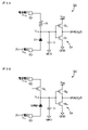
[実施例1]
実施例1は、画素アレイ部内の画素のサイズを変えることによってダイナミックレンジの拡大を図る例である。実施例1に係る画素アレイ部の構成の概略を図8に示す。
[Example 1]
The first embodiment is an example of expanding the dynamic range by changing the size of the pixels in the pixel array section. FIG. 8 shows a schematic configuration of the pixel array section according to the first embodiment.
実施例1では、画素が行列状に2次元配置されて成る画素アレイ部60において、当該画素アレイ部60内に、画素サイズが相対的に大きい第1の画素61と、第1の画素61よりも画素サイズが小さい第2の画素62とを設けた構成となっている。
In the first embodiment, in the
尚、ここでは、第1の画素61と、当該第1の画素61と同サイズの領域に配置された4個の第2の画素62とを格子状に並べた画素配置を例示したが、当該画素配置に限られるものではなく、要は、画素アレイ部60内に第1の画素61と第2の画素62とが混在する画素配置であればよい。
Note that here, the pixel arrangement in which the
第1の画素61と第2の画素62との画素サイズが異なるということは、第1の画素61と第2の画素62との受光面積が異なるということである。具体的には、図8から明らかなように、第1の画素61は、第2の画素62よりも受光面積が広く、従って、第1の画素61は、第2の画素62よりも高感度の画素である。
The fact that the pixel sizes of the
上述したように、実施例1に係る受光装置30は、画素アレイ部60内に、画素サイズ(受光面積)が相対的に大きい第1の画素61と、画素サイズ(受光面積)が相対的に小さい第2の画素62とを有する。これにより、第1の画素61によって低い入射光量の条件下でも光子を確実に検出できるし、第2の画素62によって高い入射光量の条件下でも飽和しないで検出動作を行うことができる。その結果、受光装置30のダイナミックレンジの拡大を図ることができる。
As described above, in the
(実施例1の応用例)
実施例1については、以下の応用例とすることができる。
・応用例1
第1の画素61及び第2の画素62の各出力に対して、画素サイズに応じた重み付けを行い、その和を求めて光量判定を行うようすることができる。自動車などの移動体に搭載される測距装置、例えばLIDAR(Light Detection and Ranging、Laser Imaging Detection and Ranging)装置では、レーザ光が物体で反射して戻ってくるまでの時間を観測して、物体までの距離を計算する機能の他に、反射光の光量を把握して物体を認識する機能(例えば、道路の白線を認識する機能など)がある。このような機能では、反射光の光量の判定が必要になるため、その判定結果を用いて、第1の画素61及び第2の画素62の各出力に対して、画素サイズ(受光面積)によって重み付けを行い、その和で反射光の光量を判定するようにすることができる。
(Application example of Example 1)
The first embodiment can be applied as the following examples.
・Application example 1
Each output of the
.応用例2
外乱光の大きさ(光量)によって、どちらかの画素サイズの画素のみ(第1の画素61/第2の画素62)を動作させるようにすることができる。自動車などの移動体に搭載される測距装置、例えばLIDAR装置では、レーザ光の発光を行う前に、非発光の状態で外乱光がどの程度あるのかを判定する準備モードがある。この準備モードでの判定結果を用いて、外乱光の大きさによって、画素サイズの大きい第1の画素61、及び、画素サイズの小さい第2の画素62のどちらを使用するか決めるようにすることができる。
. Application example 2
It is possible to operate only pixels of either pixel size (
・応用例3
画素サイズが相対的に大きい第1の画素61、及び、画素サイズが相対的に小さい第2の画素62を時系列で使い分けるようにすることができる。例えば、画素サイズの大きい第1の画素61、及び、画素サイズの小さい第2の画素62を交互に動作させたり、前回の評価結果に基づいて、画素サイズの大きい第1の画素61、及び、画素サイズの小さい第2の画素62のどちらを使用するか決めて使用するようにしたりすることができる。
・Application example 3
A
[実施例2]
実施例2は、画素の受光部の半導体層の厚みを変えることによってダイナミックレンジの拡大を図る例である。実施例2に係る画素アレイ部の構成の概略を図9Aに示し、受光部の断面構造を図9Bに示す。
[Example 2]
Example 2 is an example of expanding the dynamic range by changing the thickness of the semiconductor layer of the light receiving portion of the pixel. FIG. 9A shows an outline of the configuration of the pixel array portion according to Example 2, and FIG. 9B shows the cross-sectional structure of the light receiving portion.
図9Bに示すように、半導体基板、例えばp-基板71内に、半導体層であるn-ウェル72と、p+拡散層73の底面との間のpn接合によってアバランシェ増倍を発生させるSPAD素子が構成されている。p+拡散層73の周辺部には、p-ウェル74によってガードリングが形成されている。これにより、ブレークダウン電圧VBDよりも低い電圧でのソフトなブレークダウンが生じないようにしている。 As shown in FIG. 9B, in a semiconductor substrate, for example, a p - substrate 71, a pn junction between an n - well 72, which is a semiconductor layer, and the bottom surface of a p + diffusion layer 73, is a SPAD element that generates avalanche multiplication. is configured. A guard ring is formed by the p − well 74 around the p + diffusion layer 73 . This prevents soft breakdown below the breakdown voltage VBD .
上記の構造の受光部において、半導体層であるn-ウェル72の厚みtが厚いSPAD素子ほど、光入射時に電子-正孔対が発生し易いので、光子を検出できる確率PDEが高く、感度が高くなる。そこで、実施例2では、SPAD素子のn-ウェル72の厚みtを変えることにより、図9Aに示すように、画素アレイ部60内に、感度が相対的に高い第1の画素63と、感度が相対的に低い第2の画素64とを設けた構成となっている。
In the light-receiving part having the above structure, the SPAD element having the thicker thickness t of the n − well 72, which is a semiconductor layer, is more likely to generate electron-hole pairs when light is incident. get higher Therefore, in the second embodiment, by changing the thickness t of the n − well 72 of the SPAD element, as shown in FIG. is provided with a
尚、ここでは、高感度画素である第1の画素63と、低感度画素である第2の画素64とを格子状に並べた画素配置を例示したが、当該画素配置に限られるものではなく、要は、画素アレイ部60内に第1の画素63と第2の画素64とが混在する画素配置であればよい。
Although the pixel arrangement in which the
画素アレイ部60内に、高感度画素と低感度画素とを混在させるに当たって、実施例2では、高感度画素である第1の画素63について、低感度画素である第2の画素64よりもSPAD素子のn-ウェル72の厚みtを厚くする構成を採っている。
When high-sensitivity pixels and low-sensitivity pixels are mixed in the
上述したように、実施例2に係る受光装置30は、画素アレイ部60内に、n-ウェル72の厚みtが相対的に厚い第1の画素63と、n-ウェル72の厚みtが相対的に薄い第2の画素64とを有する。これにより、第1の画素63によって低い入射光量の条件下でも光子を確実に検出できるし、第2の画素64によって高い入射光量の条件下でも飽和しないで検出動作を行うことができる。その結果、受光装置30のダイナミックレンジの拡大を図ることができる。
As described above, in the
(実施例2の応用例)
実施例2については、実施例1との組み合わせで用いることもできる。すなわち、画素アレイ部60内に、n-ウェル72の厚みtが相対的に厚い第1の画素63、及び、n-ウェル72の厚みtが相対的に薄い第2の画素64に加えて、画素サイズが相対的に大きい第1の画素61、及び、画素サイズが相対的に小さい第2の画素62を有する受光装置30とすることもできる。
(Application example of Example 2)
Example 2 can also be used in combination with Example 1. That is, in the
また、実施例2についても、実施例1の応用例1乃至応用例3と同様の応用例を挙げることができる。
・応用例1
第1の画素63及び第2の画素64の各出力に対して、n-ウェル72の厚みtに応じた重み付けを行い、その和を求めて光量判定を行うようすることができる。具体例については、実施例1の応用例1と同じである。
.応用例2
外乱光の大きさ(光量)によって、どちらかのn-ウェル72の厚みtの画素のみ(第1の画素63/第2の画素64)を動作させるようにすることができる。具体例については、実施例1の応用例2と同じである。
・応用例3
n-ウェル72の厚みtが相対的に厚い第1の画素63、及び、n-ウェル72の厚みtが相対的に薄い第2の画素64を時系列で使い分けるようにすることができる。具体例については、実施例1の応用例3と同じである。
In addition, as for the second embodiment, application examples similar to the application examples 1 to 3 of the first embodiment can be given.
・Application example 1
Each output of the
. Application example 2
It is possible to operate only the pixels (
・Application example 3
A
[実施例3]
実施例3は、画素の受光部、即ち、SPAD素子のエクセスバイアス電圧VEXを変えることによってダイナミックレンジの拡大を図る例である。エクセスバイアス電圧VEXは、SPAD素子に印加するブレークダウン電圧VBD以上の過剰電圧である。実施例3に係る画素アレイ部の構成の概略を図10Aに示し、エクセスバイアス電圧VEXと、感度の指標となる確率PDEとの関係を図10Bに示す。
[Example 3]
The third embodiment is an example of expanding the dynamic range by changing the excess bias voltage V EX of the light receiving portion of the pixel, that is, the SPAD element. The excess bias voltage VEX is an excess voltage above the breakdown voltage VBD applied to the SPAD element. FIG. 10A shows an outline of the configuration of the pixel array section according to Example 3, and FIG. 10B shows the relationship between the excess bias voltage V EX and the probability PDE, which is an index of sensitivity.
図10Bから明らかなように、エクセスバイアス電圧VEXの電圧値を小さくすると、光子を検出できる確率PDE、即ちSPAD素子の感度を落とすことができるため、高光量の条件下での光飽和が起こりにくくなる。また、エクセスバイアス電圧VEXの電圧値を小さくすると、図11に示すように、SPAD出力のパルス幅、即ち、光子に反応できないデッドタイムDTを短くすることができるため、前述の理論式から、高光量の条件下での光飽和特性を改善することができる。 As is clear from FIG. 10B, when the voltage value of the excess bias voltage V EX is decreased, the photon detection probability PDE, that is, the sensitivity of the SPAD element can be decreased, so that light saturation occurs under high light intensity conditions. become difficult. Further, when the voltage value of the excess bias voltage V EX is decreased, the pulse width of the SPAD output, that is, the dead time DT in which photons cannot be reacted can be shortened as shown in FIG. Light saturation characteristics can be improved under conditions of high light intensity.
エクセスバイアス電圧VEX、光子を検出できる確率PDE、及び、光子に反応できないデッドタイムDTと、SPAD素子の特性との間には、次のような関係がある。すなわち、エクセスバイアス電圧VEXが相対的に高い、確率PDEが相対的に高い、及び、デッドタイムDTが相対的に長いSPAD素子は、感度が相対的に高いものの、相対的に飽和し易い。エクセスバイアス電圧VEXが相対的に低い、確率PDEが相対的に低い、及び、デッドタイムDTが相対的に短いSPAD素子は、感度が相対的に低いものの、相対的に飽和しにくい。 The excess bias voltage V EX , the probability PDE of detecting photons, the dead time DT of not reacting to photons, and the characteristics of the SPAD element have the following relationships. That is, a SPAD element having a relatively high excess bias voltage V EX , a relatively high probability PDE, and a relatively long dead time DT has relatively high sensitivity but is relatively easily saturated. A SPAD device with a relatively low excess bias voltage V EX , a relatively low probability PDE, and a relatively short dead time DT has relatively low sensitivity but is relatively difficult to saturate.
このように、SPAD素子にあっては、当該SPAD素子に印加するエクセスバイアス電圧VEXの電圧値によってSPAD素子の感度を調整することができる。エクセスバイアス電圧VEXの電圧値は、図3A及び図3Bにおいて、端子53に与えるアノード電圧Vbdの電圧値によって変えることができる。アノード電圧Vbdの電圧値は、画素アレイ部内の画素間で共通の固定値に設定されることが一般的である。 Thus, in the SPAD element, the sensitivity of the SPAD element can be adjusted by the voltage value of the excess bias voltage V EX applied to the SPAD element. The voltage value of the excess bias voltage V EX can be changed by the voltage value of the anode voltage V bd applied to the terminal 53 in FIGS. 3A and 3B. The voltage value of the anode voltage V bd is generally set to a common fixed value among the pixels in the pixel array section.
そこで、実施例3では、SPAD素子に印加するエクセスバイアス電圧VEXの電圧値を変えることにより、図10Aに示すように、画素アレイ部60内に、感度が相対的に高い第1の画素65と、感度が相対的に低い第2の画素66とを設けた構成となっている。 Therefore, in the third embodiment, by changing the voltage value of the excess bias voltage V EX applied to the SPAD element, as shown in FIG. , and a second pixel 66 having relatively low sensitivity.
尚、ここでは、高感度画素である第1の画素65と、低感度画素である第2の画素66とを格子状に並べた画素配置を例示したが、当該画素配置に限られるものではなく、要は、画素アレイ部60内に第1の画素65と第2の画素66とが混在する画素配置であればよい。また、エクセスバイアス電圧VEXの電圧値は、第1の画素65と第2の画素66との2段階での設定に限定されず、3段階以上に設定されてもよい。すなわち、高感度画素、中感度画素、低感度画素が混在する画素配置であってもよい。
Although the pixel arrangement in which the first pixels 65 that are high-sensitivity pixels and the second pixels 66 that are low-sensitivity pixels are arranged in a grid pattern is illustrated here, the pixel arrangement is not limited to this. In short, the pixel arrangement may be such that the first pixels 65 and the second pixels 66 are mixed in the
上述したように、実施例3に係る受光装置30は、画素アレイ部60内に、エクセスバイアス電圧VEXが相対的に高い第1の画素65と、エクセスバイアス電圧VEXが相対的に低い第2の画素66とを有する。これにより、第1の画素65によって低い入射光量の条件下でも光子を確実に検出できるし、第2の画素66によって高い入射光量の条件下でも飽和しないで検出動作を行うことができる。その結果、受光装置30のダイナミックレンジの拡大を図ることができる。
As described above, in the
(実施例3の応用例)
実施例3については、実施例1との組み合わせ、実施例2との組み合わせ、あるいは、実施例1及び実施例2との組み合わせで用いることもできる。すなわち、画素アレイ部60内に、エクセスバイアス電圧VEXが相対的に高い第1の画素65、及び、エクセスバイアス電圧VEXが相対的に低い第2の画素66に加えて、画素サイズが相対的に大きい第1の画素61、及び、画素サイズが相対的に小さい第2の画素62を有する受光装置30とすることもできる。
(Example of application of Example 3)
Example 3 can be used in combination with Example 1, in combination with Example 2, or in combination with Example 1 and Example 2. That is, in addition to the first pixels 65 having a relatively high excess bias voltage V EX and the second pixels 66 having a relatively low excess bias voltage V EX in the
また、画素アレイ部60内に、エクセスバイアス電圧VEXが相対的に高い第1の画素65、及び、エクセスバイアス電圧VEXが相対的に低い第2の画素66に加えて、n-ウェル72の厚みtが相対的に厚い第1の画素63、及び、n-ウェル72の厚みtが相対的に薄い第2の画素64を有する受光装置30とすることもできる。
Further, in the
あるいは、画素アレイ部60内に、エクセスバイアス電圧VEXが相対的に高い第1の画素65、及び、エクセスバイアス電圧VEXが相対的に低い第2の画素66に加えて、画素サイズが相対的に大きい第1の画素61、及び、画素サイズが相対的に小さい第2の画素62、並びに、n-ウェル72の厚みtが相対的に厚い第1の画素63、及び、n-ウェル72の厚みtが相対的に薄い第2の画素64を有する受光装置30とすることもできる。
Alternatively, in addition to the first pixel 65 having a relatively high excess bias voltage V EX and the second pixel 66 having a relatively low excess bias voltage V EX in the
また、実施例3についても、実施例1の応用例1乃至応用例3と同様の応用例を挙げることができる。
・応用例1
第1の画素65及び第2の画素66の各出力に対して、エクセスバイアス電圧VEXに応じた重み付けを行い、その和を求めて光量判定を行うようすることができる。具体例については、実施例1の応用例1と同じである。
.応用例2
外乱光の大きさ(光量)によって、どちらかのエクセスバイアス電圧VEXの画素のみ(第1の画素65/第2の画素66)を動作させるようにすることができる。具体例については、実施例1の応用例2と同じである。
・応用例3
エクセスバイアス電圧VEXが相対的に高い第1の画素65、及び、エクセスバイアス電圧VEXが相対的に低い第2の画素66を時系列で使い分けるようにすることができる。具体例については、実施例1の応用例3と同じである。
Further, as for the third embodiment, application examples similar to the application examples 1 to 3 of the first embodiment can be given.
・Application example 1
Each output of the first pixel 65 and the second pixel 66 can be weighted according to the excess bias voltage VEX , and the sum of the weights can be obtained to determine the amount of light. A specific example is the same as the application example 1 of the first embodiment.
. Application example 2
It is possible to operate only pixels (first pixel 65/second pixel 66) with either excess bias voltage V EX depending on the magnitude (light amount) of ambient light. A specific example is the same as the application example 2 of the first embodiment.
・Application example 3
The first pixels 65 with a relatively high excess bias voltage V EX and the second pixels 66 with a relatively low excess bias voltage V EX can be selectively used in chronological order. A specific example is the same as the application example 3 of the first embodiment.
[実施例4]
実施例4は、実施例3の変形例であり、外乱光の大きさ(光量)に応じてエクセスバイアス電圧VEXの電圧値の大きさを調整する例である。実施例4に係る受光装置の構成の概略を図12に示す。
[Example 4]
The fourth embodiment is a modification of the third embodiment, and is an example in which the magnitude of the excess bias voltage V EX is adjusted according to the magnitude (light amount) of ambient light. FIG. 12 shows the outline of the configuration of the light receiving device according to the fourth embodiment.
実施例4では、実施例3の場合と同様に、SPAD素子のエクセスバイアス電圧VEXを変えることによってダイナミックレンジの拡大を図るとともに、外乱光の大きさ(光量)に応じてエクセスバイアス電圧VEXの電圧値の大きさを調整するようにする。そのために、実施例4に係る受光装置は、画素回路50の端子53に印加するアノード電圧Vbdを設定するアノード電圧設定部71、及び、外乱光の大きさ(光量)を検出する外乱光検出部72を備えている。
In the fourth embodiment, as in the case of the third embodiment, the excess bias voltage V EX of the SPAD element is changed to expand the dynamic range, and the excess bias voltage V EX is adjusted in accordance with the magnitude of disturbance light (light amount). to adjust the magnitude of the voltage value of For this reason, the light receiving device according to the fourth embodiment includes an anode
アノード電圧設定部71は、外乱光検出部72が検出した外乱光の大きさに応じて、連続的に、あるいは、段階的に、アノード電圧Vbdの電圧値を設定する。これにより、エクセスバイアス電圧VEXの電圧値の大きさが、外乱光の大きさに応じて、連続的に、あるいは、段階的に調整される。その結果、画素のサイズ(受光面積)や、受光部の半導体層の厚みを変えたりしなくても、画素の感度を変えることができ、ダイナミックレンジの拡大を図ることができる。
The anode
外乱光検出部72としては、周知の光センサを用いることができる。あるいは、LIDAR装置では、レーザ光の発光を行う前に、非発光の状態で外乱光がどの程度あるのかを判定する準備モードがある。従って、自動車などの移動体に搭載する測距装置の受光装置として、実施例4に係る受光装置を用いる場合には、準備モードで判定される外乱光の大きさを、アノード電圧設定部71の入力として用いるようにすることができる。
A well-known optical sensor can be used as the ambient
尚、実施例4に係る受光装置の画素回路50として、図3Aに示す画素回路を用いる場合を例に挙げて説明したが、図3Bに示す画素回路を用いる場合も同じである。
Although the case where the pixel circuit shown in FIG. 3A is used as the
<本開示に係る技術の適用例>
本開示に係る技術は、様々な製品に適用することができる。以下に、より具体的な適用例について説明する。例えば、本開示に係る技術は、自動車、電気自動車、ハイブリッド電気自動車、自動二輪車、自転車、パーソナルモビリティ、飛行機、ドローン、船舶、ロボット、建設機械、農業機械(トラクター)などのいずれかの種類の移動体に搭載される測距装置として実現されてもよい。
<Application example of technology according to the present disclosure>
The technology according to the present disclosure can be applied to various products. A more specific application example will be described below. For example, the technology according to the present disclosure can be applied to any type of movement such as automobiles, electric vehicles, hybrid electric vehicles, motorcycles, bicycles, personal mobility, airplanes, drones, ships, robots, construction machinery, agricultural machinery (tractors), etc. It may be implemented as a range finder mounted on the body.
[移動体]
図13は、本開示に係る技術が適用され得る移動体制御システムの一例である車両制御システム7000の概略的な構成例を示すブロック図である。車両制御システム7000は、通信ネットワーク7010を介して接続された複数の電子制御ユニットを備える。図13に示した例では、車両制御システム7000は、駆動系制御ユニット7100、ボディ系制御ユニット7200、バッテリ制御ユニット7300、車外情報検出ユニット7400、車内情報検出ユニット7500、及び統合制御ユニット7600を備える。これらの複数の制御ユニットを接続する通信ネットワーク7010は、例えば、CAN(Controller Area Network)、LIN(Local Interconnect Network)、LAN(Local Area Network)又はFlexRay(登録商標)等の任意の規格に準拠した車載通信ネットワークであってよい。
[Moving body]
FIG. 13 is a block diagram showing a schematic configuration example of a
各制御ユニットは、各種プログラムにしたがって演算処理を行うマイクロコンピュータと、マイクロコンピュータにより実行されるプログラム又は各種演算に用いられるパラメータ等を記憶する記憶部と、各種制御対象の装置を駆動する駆動回路とを備える。各制御ユニットは、通信ネットワーク7010を介して他の制御ユニットとの間で通信を行うためのネットワークI/Fを備えるとともに、車内外の装置又はセンサ等との間で、有線通信又は無線通信により通信を行うための通信I/Fを備える。図13では、統合制御ユニット7600の機能構成として、マイクロコンピュータ7610、汎用通信I/F7620、専用通信I/F7630、測位部7640、ビーコン受信部7650、車内機器I/F7660、音声画像出力部7670、車載ネットワークI/F7680及び記憶部7690が図示されている。他の制御ユニットも同様に、マイクロコンピュータ、通信I/F及び記憶部等を備える。
Each control unit includes a microcomputer that performs arithmetic processing according to various programs, a storage unit that stores programs executed by the microcomputer or parameters used in various calculations, and a drive circuit that drives various devices to be controlled. Prepare. Each control unit has a network I/F for communicating with other control units via a
駆動系制御ユニット7100は、各種プログラムにしたがって車両の駆動系に関連する装置の動作を制御する。例えば、駆動系制御ユニット7100は、内燃機関又は駆動用モータ等の車両の駆動力を発生させるための駆動力発生装置、駆動力を車輪に伝達するための駆動力伝達機構、車両の舵角を調節するステアリング機構、及び、車両の制動力を発生させる制動装置等の制御装置として機能する。駆動系制御ユニット7100は、ABS(Antilock Brake System)又はESC(Electronic Stability Control)等の制御装置としての機能を有してもよい。
Drive
駆動系制御ユニット7100には、車両状態検出部7110が接続される。車両状態検出部7110には、例えば、車体の軸回転運動の角速度を検出するジャイロセンサ、車両の加速度を検出する加速度センサ、あるいは、アクセルペダルの操作量、ブレーキペダルの操作量、ステアリングホイールの操舵角、エンジン回転数又は車輪の回転速度等を検出するためのセンサのうちの少なくとも一つが含まれる。駆動系制御ユニット7100は、車両状態検出部7110から入力される信号を用いて演算処理を行い、内燃機関、駆動用モータ、電動パワーステアリング装置又はブレーキ装置等を制御する。
A vehicle
ボディ系制御ユニット7200は、各種プログラムにしたがって車体に装備された各種装置の動作を制御する。例えば、ボディ系制御ユニット7200は、キーレスエントリシステム、スマートキーシステム、パワーウィンドウ装置、あるいは、ヘッドランプ、バックランプ、ブレーキランプ、ウィンカー又はフォグランプ等の各種ランプの制御装置として機能する。この場合、ボディ系制御ユニット7200には、鍵を代替する携帯機から発信される電波又は各種スイッチの信号が入力され得る。ボディ系制御ユニット7200は、これらの電波又は信号の入力を受け付け、車両のドアロック装置、パワーウィンドウ装置、ランプ等を制御する。
Body
バッテリ制御ユニット7300は、各種プログラムにしたがって駆動用モータの電力供給源である二次電池7310を制御する。例えば、バッテリ制御ユニット7300には、二次電池7310を備えたバッテリ装置から、バッテリ温度、バッテリ出力電圧又はバッテリの残存容量等の情報が入力される。バッテリ制御ユニット7300は、これらの信号を用いて演算処理を行い、二次電池7310の温度調節制御又はバッテリ装置に備えられた冷却装置等の制御を行う。
A
車外情報検出ユニット7400は、車両制御システム7000を搭載した車両の外部の情報を検出する。例えば、車外情報検出ユニット7400には、撮像部7410及び車外情報検出部7420のうちの少なくとも一方が接続される。撮像部7410には、ToF(Time Of Flight)カメラ、ステレオカメラ、単眼カメラ、赤外線カメラ及びその他のカメラのうちの少なくとも一つが含まれる。車外情報検出部7420には、例えば、現在の天候又は気象を検出するための環境センサ、あるいは、車両制御システム7000を搭載した車両の周囲の他の車両、障害物又は歩行者等を検出するための周囲情報検出センサのうちの少なくとも一つが含まれる。
External
環境センサは、例えば、雨天を検出する雨滴センサ、霧を検出する霧センサ、日照度合いを検出する日照センサ、及び降雪を検出する雪センサのうちの少なくとも一つであってよい。周囲情報検出センサは、超音波センサ、レーダ装置及びLIDAR(Light Detection and Ranging、Laser Imaging Detection and Ranging)装置のうちの少なくとも一つであってよい。これらの撮像部7410及び車外情報検出部7420は、それぞれ独立したセンサないし装置として備えられてもよいし、複数のセンサないし装置が統合された装置として備えられてもよい。
The environment sensor may be, for example, at least one of a raindrop sensor that detects rainy weather, a fog sensor that detects fog, a sunshine sensor that detects the degree of sunshine, and a snow sensor that detects snowfall. The ambient information detection sensor may be at least one of an ultrasonic sensor, a radar device, and a LIDAR (Light Detection and Ranging, Laser Imaging Detection and Ranging) device. These
ここで、図14は、撮像部7410及び車外情報検出部7420の設置位置の例を示す。撮像部7910,7912,7914,7916,7918は、例えば、車両7900のフロントノーズ、サイドミラー、リアバンパ、バックドア及び車室内のフロントガラスの上部のうちの少なくとも一つの位置に設けられる。フロントノーズに備えられる撮像部7910及び車室内のフロントガラスの上部に備えられる撮像部7918は、主として車両7900の前方の画像を取得する。サイドミラーに備えられる撮像部7912,7914は、主として車両7900の側方の画像を取得する。リアバンパ又はバックドアに備えられる撮像部7916は、主として車両7900の後方の画像を取得する。車室内のフロントガラスの上部に備えられる撮像部7918は、主として先行車両又は、歩行者、障害物、信号機、交通標識又は車線等の検出に用いられる。
Here, FIG. 14 shows an example of installation positions of the
尚、図14には、それぞれの撮像部7910,7912,7914,7916の撮影範囲の一例が示されている。撮像範囲aは、フロントノーズに設けられた撮像部7910の撮像範囲を示し、撮像範囲b,cは、それぞれサイドミラーに設けられた撮像部7912,7914の撮像範囲を示し、撮像範囲dは、リアバンパ又はバックドアに設けられた撮像部7916の撮像範囲を示す。例えば、撮像部7910,7912,7914,7916で撮像された画像データが重ね合わせられることにより、車両7900を上方から見た俯瞰画像が得られる。
Note that FIG. 14 shows an example of the imaging range of each of the
車両7900のフロント、リア、サイド、コーナ及び車室内のフロントガラスの上部に設けられる車外情報検出部7920,7922,7924,7926,7928,7930は、例えば超音波センサ又はレーダ装置であってよい。車両7900のフロントノーズ、リアバンパ、バックドア及び車室内のフロントガラスの上部に設けられる車外情報検出部7920,7926,7930は、例えばLIDAR装置であってよい。これらの車外情報検出部7920~7930は、主として先行車両、歩行者又は障害物等の検出に用いられる。
The vehicle
図13に戻って説明を続ける。車外情報検出ユニット7400は、撮像部7410に車外の画像を撮像させるとともに、撮像された画像データを受信する。また、車外情報検出ユニット7400は、接続されている車外情報検出部7420から検出情報を受信する。車外情報検出部7420が超音波センサ、レーダ装置又はLIDAR装置である場合には、車外情報検出ユニット7400は、超音波又は電磁波等を発信させるとともに、受信された反射波の情報を受信する。車外情報検出ユニット7400は、受信した情報に基づいて、人、車、障害物、標識又は路面上の文字等の物体検出処理又は距離検出処理を行ってもよい。車外情報検出ユニット7400は、受信した情報に基づいて、降雨、霧又は路面状況等を認識する環境認識処理を行ってもよい。車外情報検出ユニット7400は、受信した情報に基づいて、車外の物体までの距離を算出してもよい。
Returning to FIG. 13, the description continues. The vehicle exterior
また、車外情報検出ユニット7400は、受信した画像データに基づいて、人、車、障害物、標識又は路面上の文字等を認識する画像認識処理又は距離検出処理を行ってもよい。車外情報検出ユニット7400は、受信した画像データに対して歪補正又は位置合わせ等の処理を行うとともに、異なる撮像部7410により撮像された画像データを合成して、俯瞰画像又はパノラマ画像を生成してもよい。車外情報検出ユニット7400は、異なる撮像部7410により撮像された画像データを用いて、視点変換処理を行ってもよい。
Further, the vehicle exterior
車内情報検出ユニット7500は、車内の情報を検出する。車内情報検出ユニット7500には、例えば、運転者の状態を検出する運転者状態検出部7510が接続される。運転者状態検出部7510は、運転者を撮像するカメラ、運転者の生体情報を検出する生体センサ又は車室内の音声を集音するマイク等を含んでもよい。生体センサは、例えば、座面又はステアリングホイール等に設けられ、座席に座った搭乗者又はステアリングホイールを握る運転者の生体情報を検出する。車内情報検出ユニット7500は、運転者状態検出部7510から入力される検出情報に基づいて、運転者の疲労度合い又は集中度合いを算出してもよいし、運転者が居眠りをしていないかを判別してもよい。車内情報検出ユニット7500は、集音された音声信号に対してノイズキャンセリング処理等の処理を行ってもよい。
The vehicle interior
統合制御ユニット7600は、各種プログラムにしたがって車両制御システム7000内の動作全般を制御する。統合制御ユニット7600には、入力部7800が接続されている。入力部7800は、例えば、タッチパネル、ボタン、マイクロフォン、スイッチ又はレバー等、搭乗者によって入力操作され得る装置によって実現される。統合制御ユニット7600には、マイクロフォンにより入力される音声を音声認識することにより得たデータが入力されてもよい。入力部7800は、例えば、赤外線又はその他の電波を利用したリモートコントロール装置であってもよいし、車両制御システム7000の操作に対応した携帯電話又はPDA(Personal Digital Assistant)等の外部接続機器であってもよい。入力部7800は、例えばカメラであってもよく、その場合搭乗者はジェスチャにより情報を入力することができる。あるいは、搭乗者が装着したウェアラブル装置の動きを検出することで得られたデータが入力されてもよい。さらに、入力部7800は、例えば、上記の入力部7800を用いて搭乗者等により入力された情報に基づいて入力信号を生成し、統合制御ユニット7600に出力する入力制御回路などを含んでもよい。搭乗者等は、この入力部7800を操作することにより、車両制御システム7000に対して各種のデータを入力したり処理動作を指示したりする。
The
記憶部7690は、マイクロコンピュータにより実行される各種プログラムを記憶するROM(Read Only Memory)、及び各種パラメータ、演算結果又はセンサ値等を記憶するRAM(Random Access Memory)を含んでいてもよい。また、記憶部7690は、HDD(Hard Disc Drive)等の磁気記憶デバイス、半導体記憶デバイス、光記憶デバイス又は光磁気記憶デバイス等によって実現してもよい。
The
汎用通信I/F7620は、外部環境7750に存在する様々な機器との間の通信を仲介する汎用的な通信I/Fである。汎用通信I/F7620は、GSM(登録商標)(Global System of Mobile communications)、WiMAX、LTE(Long Term Evolution)若しくはLTE-A(LTE-Advanced)などのセルラー通信プロトコル、又は無線LAN(Wi-Fi(登録商標)ともいう)、Bluetooth(登録商標)などのその他の無線通信プロトコルを実装してよい。汎用通信I/F7620は、例えば、基地局又はアクセスポイントを介して、外部ネットワーク(例えば、インターネット、クラウドネットワーク又は事業者固有のネットワーク)上に存在する機器(例えば、アプリケーションサーバ又は制御サーバ)へ接続してもよい。また、汎用通信I/F7620は、例えばP2P(Peer To Peer)技術を用いて、車両の近傍に存在する端末(例えば、運転者、歩行者若しくは店舗の端末、又はMTC(Machine Type Communication)端末)と接続してもよい。
General-purpose communication I/
専用通信I/F7630は、車両における使用を目的として策定された通信プロトコルをサポートする通信I/Fである。専用通信I/F7630は、例えば、下位レイヤのIEEE802.11pと上位レイヤのIEEE1609との組合せであるWAVE(Wireless Access in Vehicle Environment)、DSRC(Dedicated Short Range Communications)、又はセルラー通信プロトコルといった標準プロトコルを実装してよい。専用通信I/F7630は、典型的には、車車間(Vehicle to Vehicle)通信、路車間(Vehicle to Infrastructure)通信、車両と家との間(Vehicle to Home)の通信及び歩車間(Vehicle to Pedestrian)通信のうちの1つ以上を含む概念であるV2X通信を遂行する。
Dedicated communication I/
測位部7640は、例えば、GNSS(Global Navigation Satellite System)衛星からのGNSS信号(例えば、GPS(Global Positioning System)衛星からのGPS信号)を受信して測位を実行し、車両の緯度、経度及び高度を含む位置情報を生成する。尚、測位部7640は、無線アクセスポイントとの信号の交換により現在位置を特定してもよく、又は測位機能を有する携帯電話、PHS若しくはスマートフォンといった端末から位置情報を取得してもよい。
The
ビーコン受信部7650は、例えば、道路上に設置された無線局等から発信される電波あるいは電磁波を受信し、現在位置、渋滞、通行止め又は所要時間等の情報を取得する。尚、ビーコン受信部7650の機能は、上述した専用通信I/F7630に含まれてもよい。
The
車内機器I/F7660は、マイクロコンピュータ7610と車内に存在する様々な車内機器7760との間の接続を仲介する通信インタフェースである。車内機器I/F7660は、無線LAN、Bluetooth(登録商標)、NFC(Near Field Communication)又はWUSB(Wireless USB)といった無線通信プロトコルを用いて無線接続を確立してもよい。また、車内機器I/F7660は、図示しない接続端子(及び、必要であればケーブル)を介して、USB(Universal Serial Bus)、HDMI(登録商標)(High-Definition Multimedia Interface)、又はMHL(Mobile High-definition Link)等の有線接続を確立してもよい。車内機器7760は、例えば、搭乗者が有するモバイル機器若しくはウェアラブル機器、又は車両に搬入され若しくは取り付けられる情報機器のうちの少なくとも1つを含んでいてもよい。また、車内機器7760は、任意の目的地までの経路探索を行うナビゲーション装置を含んでいてもよい。車内機器I/F7660は、これらの車内機器7760との間で、制御信号又はデータ信号を交換する。
In-vehicle equipment I/
車載ネットワークI/F7680は、マイクロコンピュータ7610と通信ネットワーク7010との間の通信を仲介するインタフェースである。車載ネットワークI/F7680は、通信ネットワーク7010によりサポートされる所定のプロトコルに則して、信号等を送受信する。
In-vehicle network I/
統合制御ユニット7600のマイクロコンピュータ7610は、汎用通信I/F7620、専用通信I/F7630、測位部7640、ビーコン受信部7650、車内機器I/F7660及び車載ネットワークI/F7680のうちの少なくとも一つを介して取得される情報に基づき、各種プログラムにしたがって、車両制御システム7000を制御する。例えば、マイクロコンピュータ7610は、取得される車内外の情報に基づいて、駆動力発生装置、ステアリング機構又は制動装置の制御目標値を演算し、駆動系制御ユニット7100に対して制御指令を出力してもよい。例えば、マイクロコンピュータ7610は、車両の衝突回避あるいは衝撃緩和、車間距離に基づく追従走行、車速維持走行、車両の衝突警告、又は車両のレーン逸脱警告等を含むADAS(Advanced Driver Assistance System)の機能実現を目的とした協調制御を行ってもよい。また、マイクロコンピュータ7610は、取得される車両の周囲の情報に基づいて駆動力発生装置、ステアリング機構又は制動装置等を制御することにより、運転者の操作に拠らずに自律的に走行する自動運転等を目的とした協調制御を行ってもよい。
The
マイクロコンピュータ7610は、汎用通信I/F7620、専用通信I/F7630、測位部7640、ビーコン受信部7650、車内機器I/F7660及び車載ネットワークI/F7680のうちの少なくとも一つを介して取得される情報に基づき、車両と周辺の構造物や人物等の物体との間の3次元距離情報を生成し、車両の現在位置の周辺情報を含むローカル地図情報を作成してもよい。また、マイクロコンピュータ7610は、取得される情報に基づき、車両の衝突、歩行者等の近接又は通行止めの道路への進入等の危険を予測し、警告用信号を生成してもよい。警告用信号は、例えば、警告音を発生させたり、警告ランプを点灯させたりするための信号であってよい。
音声画像出力部7670は、車両の搭乗者又は車外に対して、視覚的又は聴覚的に情報を通知することが可能な出力装置へ音声及び画像のうちの少なくとも一方の出力信号を送信する。図13の例では、出力装置として、オーディオスピーカ7710、表示部7720及びインストルメントパネル7730が例示されている。表示部7720は、例えば、オンボードディスプレイ及びヘッドアップディスプレイの少なくとも一つを含んでいてもよい。表示部7720は、AR(Augmented Reality)表示機能を有していてもよい。出力装置は、これらの装置以外の、ヘッドホン、搭乗者が装着する眼鏡型ディスプレイ等のウェアラブルデバイス、プロジェクタ又はランプ等の他の装置であってもよい。出力装置が表示装置の場合、表示装置は、マイクロコンピュータ7610が行った各種処理により得られた結果又は他の制御ユニットから受信された情報を、テキスト、イメージ、表、グラフ等、様々な形式で視覚的に表示する。また、出力装置が音声出力装置の場合、音声出力装置は、再生された音声データ又は音響データ等からなるオーディオ信号をアナログ信号に変換して聴覚的に出力する。
The audio/
尚、図13に示した例において、通信ネットワーク7010を介して接続された少なくとも二つの制御ユニットが一つの制御ユニットとして一体化されてもよい。あるいは、個々の制御ユニットが、複数の制御ユニットにより構成されてもよい。さらに、車両制御システム7000が、図示されていない別の制御ユニットを備えてもよい。また、上記の説明において、いずれかの制御ユニットが担う機能の一部又は全部を、他の制御ユニットに持たせてもよい。つまり、通信ネットワーク7010を介して情報の送受信がされるようになっていれば、所定の演算処理が、いずれかの制御ユニットで行われるようになってもよい。同様に、いずれかの制御ユニットに接続されているセンサ又は装置が、他の制御ユニットに接続されるとともに、複数の制御ユニットが、通信ネットワーク7010を介して相互に検出情報を送受信してもよい。
In the example shown in FIG. 13, at least two control units connected via the
以上、本開示に係る技術が適用され得る車両制御システムの一例について説明した。本開示に係る技術は、以上説明した構成のうち、例えば、撮像部7910,7912,7914,7916,7918や車外情報検出部7920,7922,7924,7926,7928,7930に適用され得る。そして、本開示に係る技術を適用することにより、受光装置のダイナミックレンジの拡大を図ることができ、弱い入射光にも反応でき、且つ、強い入射光で飽和しない動作を行うことができるため、例えば、撮像対象を高精度にて検出可能な車両制御システムを構築できる。
An example of a vehicle control system to which the technology according to the present disclosure can be applied has been described above. The technology according to the present disclosure can be applied to, for example, the
<本開示がとることができる構成>
本開示は、以下のような構成をとることもできる。
<Configuration that the present disclosure can take>
The present disclosure can also be configured as follows.
≪A.受光装置≫
[A-1]光子の受光に応じて信号を発生する受光部をそれぞれ含む複数の画素を有する画素アレイ部を備え、
画素アレイ部は、第1感度の画素、及び、第1感度の画素よりも感度が低い第2感度の画素を有する、
受光装置。
[A-2]第1感度は、所定の光強度よりも弱い入射光を検出できる感度であり、
第2感度は、所定の光量以下で飽和しない感度である、
上記[A-1]に記載の受光装置。
[A-3]第1感度の画素は、第2感度の画素よりも受光面積が広い、
上記[A-2]に記載の受光装置。
[A-4]第1感度の画素は、第2感度の画素よりも受光部の半導体層の厚みが厚い、
上記[A-2]に記載の受光装置。
[A-5]第1感度の画素は、第2感度の画素よりもエクセスバイアス電圧の電圧値が高い、
上記[A-2]に記載の受光装置。
[A-6]エクセスバイアス電圧の電圧値は、受光部のアノード電極に印加するアノード電圧の電圧値によって設定される、
上記[A-5]に記載の受光装置。
[A-7]外乱光の大きさに応じて、アノード電圧の電圧値を設定する、
上記[A-6]に記載の受光装置。
[A-8]受光部は、単一光子アバランシェダイオードから成る、
上記[A-1]乃至上記[A-7]のいずれかに記載の受光装置。
≪A. Light receiving device≫
[A-1] A pixel array section having a plurality of pixels each including a light receiving section that generates a signal in response to receiving a photon;
The pixel array unit has pixels with a first sensitivity and pixels with a second sensitivity that is lower in sensitivity than the pixels with the first sensitivity.
photodetector.
[A-2] The first sensitivity is a sensitivity that can detect incident light that is weaker than a predetermined light intensity,
The second sensitivity is a sensitivity that does not saturate below a predetermined amount of light.
The light receiving device according to [A-1] above.
[A-3] The pixels with the first sensitivity have a larger light-receiving area than the pixels with the second sensitivity,
The light receiving device according to [A-2] above.
[A-4] The pixels with the first sensitivity have a thicker semiconductor layer in the light-receiving part than the pixels with the second sensitivity,
The light receiving device according to [A-2] above.
[A-5] The pixel with the first sensitivity has a higher voltage value of the excess bias voltage than the pixel with the second sensitivity,
The light receiving device according to [A-2] above.
[A-6] The voltage value of the excess bias voltage is set by the voltage value of the anode voltage applied to the anode electrode of the light receiving section.
The light receiving device according to [A-5] above.
[A-7] setting the voltage value of the anode voltage according to the magnitude of the disturbance light;
The light receiving device according to [A-6] above.
[A-8] The light receiving unit consists of a single-photon avalanche diode,
The light receiving device according to any one of [A-1] to [A-7] above.
≪B.測距装置≫
[B-1]測定対象物に対して光を照射する光源、及び、
測定対象物で反射された光を受光する受光装置を備え、
受光装置は、
光子の受光に応じて信号を発生する受光部をそれぞれ含む複数の画素を有する画素アレイ部を備え、
画素アレイ部は、第1感度の画素、及び、第1感度の画素よりも感度が低い第2感度の画素を有する、
測距装置。
[B-2]第1感度は、所定の光強度よりも弱い入射光を検出できる感度であり、
第2感度は、所定の光量以下で飽和しない感度である、
上記[B-1]に記載の測距装置。
[B-3]第1感度の画素は、第2感度の画素よりも受光面積が広い、
上記[B-2]に記載の測距装置。
[B-4]第1感度の画素は、第2感度の画素よりも受光部の半導体層の厚みが厚い、
上記[B-2]に記載の測距装置。
[B-5]第1感度の画素は、第2感度の画素よりもエクセスバイアス電圧の電圧値が高い、
上記[B-2]に記載の測距装置。
[B-6]エクセスバイアス電圧の電圧値は、受光部のアノード電極に印加するアノード電圧の電圧値によって設定される、
上記[B-5]に記載の測距装置。
[B-7]外乱光の大きさに応じて、アノード電圧の電圧値を設定する、
上記[B-6]に記載の測距装置。
[B-8]受光部は、単一光子アバランシェダイオードから成る、
上記[B-1]乃至上記[B-7]のいずれかに記載の測距装置。
«B. Rangefinder≫
[B-1] A light source that irradiates light to an object to be measured, and
Equipped with a light receiving device that receives light reflected by the object to be measured,
The light receiving device
A pixel array section having a plurality of pixels each including a light receiving section that generates a signal in response to receiving a photon,
The pixel array unit has pixels with a first sensitivity and pixels with a second sensitivity that is lower in sensitivity than the pixels with the first sensitivity.
rangefinder.
[B-2] The first sensitivity is a sensitivity that can detect incident light that is weaker than a predetermined light intensity,
The second sensitivity is a sensitivity that does not saturate below a predetermined amount of light.
The distance measuring device according to [B-1] above.
[B-3] The pixels with the first sensitivity have a larger light-receiving area than the pixels with the second sensitivity,
The distance measuring device according to [B-2] above.
[B-4] The pixels with the first sensitivity have a thicker semiconductor layer in the light-receiving part than the pixels with the second sensitivity,
The distance measuring device according to [B-2] above.
[B-5] The pixel with the first sensitivity has a higher voltage value of the excess bias voltage than the pixel with the second sensitivity,
The distance measuring device according to [B-2] above.
[B-6] The voltage value of the excess bias voltage is set by the voltage value of the anode voltage applied to the anode electrode of the light receiving section.
The distance measuring device according to [B-5] above.
[B-7] setting the voltage value of the anode voltage according to the magnitude of the disturbance light;
The distance measuring device according to [B-6] above.
[B-8] The light receiving unit consists of a single-photon avalanche diode,
The distance measuring device according to any one of [B-1] to [B-7] above.
1・・・測距装置、10・・・被写体(測定対象物)、20・・・光源、21・・・レーザドライバ、22・・・レーザ光源、23・・・拡散レンズ、30・・・受光装置、31・・・受光レンズ、32・・・光センサ、33・・・回路部、40・・・制御部、50・・・画素回路、51・・・SPAD素子、60・・・画素アレイ部、61,63,65・・・第1の画素(高感度画素)、62,64,66・・・第2の画素(低感度画素)、71・・・アノード電圧設定部、72・・・外乱光検出部
DESCRIPTION OF
Claims (11)
複数の画素は、第1の光子を検出する第1感度を有する第1の画素、第2の光子を検出する第2感度を有する第2の画素、第3の光子を検出する第3の感度を有する第3の画素、及び第4の光子を検出する第4の感度を有すると共に第n行のうち第1の画素の列の隣の列に配置された第4の画素、を含み、
第1の画素の受光面積は、第2の画素の受光面積および第3の画素の受光面積の各々よりも広く、
第2の感度、第3の感度及び第4の感度の各々は第1の感度よりも低く、
第1の画素、第2の画素、および第3の画素は、画素アレイ部の同じ列に配置され、
第1の画素は第n行目、第2の画素は第n+1行目、第3の画素は第n-1行目に配置されている
受光装置。 a pixel array portion having a plurality of pixels each including a single light receiving element configured to generate a signal in response to detection of photons;
The plurality of pixels includes a first pixel having a first sensitivity to detect a first photon, a second pixel having a second sensitivity to detect a second photon, and a third sensitivity to detect a third photon. and a fourth pixel having a fourth sensitivity to detect a fourth photon and located in the nth row in the column next to the first pixel column;
the light-receiving area of the first pixel is larger than each of the light-receiving area of the second pixel and the light-receiving area of the third pixel;
each of the second sensitivity, the third sensitivity and the fourth sensitivity is lower than the first sensitivity;
the first pixel, the second pixel, and the third pixel are arranged in the same column of the pixel array section;
The first pixel is arranged in the n-th row, the second pixel is arranged in the (n+1)th row, and the third pixel is arranged in the ( n-1)th row.
請求項1に記載の受光装置。 2. The light receiving device of claim 1, wherein the operation of the first pixel or the operation of the second pixel is arranged to switch depending on the intensity of the ambient light.
請求項1に記載の受光装置。 The light receiving device according to claim 1, wherein the thickness of the semiconductor layer of the light receiving element in the first pixel is thicker than the thickness of the semiconductor layer of the light receiving element in the second pixel.
電圧源は、第1のエクセスバイアス電圧を第1の画素に供給すると共に第2のエクセスバイアス電圧を第2の画素に供給するように構成され、
第1のエクセスバイアス電圧は第2のエクセスバイアス電圧よりも高い
請求項1に記載の受光装置。 further comprising at least one voltage source;
a voltage source configured to supply a first excess bias voltage to the first pixel and a second excess bias voltage to the second pixel;
The light receiving device according to claim 1, wherein the first excess bias voltage is higher than the second excess bias voltage.
請求項4に記載の受光装置。 5. The light receiving device according to claim 4, wherein the first excess bias voltage is set by an anode voltage applied to the anode electrode of the light receiving element in the first pixel.
アノード電圧は、外乱光の光量に応じて設定される
請求項5に記載の受光装置。 Further comprising a disturbance light detection unit configured to detect the intensity of disturbance light,
The light receiving device according to claim 5, wherein the anode voltage is set according to the amount of ambient light.
請求項1に記載の受光装置。 The light receiving device according to claim 1, wherein the light receiving element includes a single-photon avalanche diode.
測定対象物によって反射された光を受信する受光装置と
を備え、
受光装置は、少なくとも1つの光子の受光に応じて信号を発生する単一の受光素子をそれぞれ含む複数の画素を有する画素アレイ部を備え、
画素アレイ部は、第1の光子を検出する第1の感度を有する第1の画素、第2の光子を検出する第2感度を有する第2の画素、第3の光子を検出する第3の感度を有する第3の画素、及び第4の光子を検出する第4の感度を有すると共に第n行のうち第1の画素の列の隣の列に配置された第4の画素、を含み、
第1の画素の受光面積は、第2の画素の受光面積および第3の画素の受光面積の各々よりも広く、
第2の感度、第3の感度及び第4の感度の各々は第1の感度よりも低く、
第1の画素、第2の画素、および第3の画素は、画素アレイ部の同じ列に配置され、
第1の画素は第n行目、第2の画素は第n+1行目、第3の画素は第n-1行目に配置されている
測距装置。 a light source that irradiates the object to be measured with light;
a light receiving device for receiving light reflected by the object to be measured,
The light-receiving device includes a pixel array section having a plurality of pixels each including a single light-receiving element that generates a signal in response to receiving at least one photon,
The pixel array section includes first pixels having a first sensitivity for detecting the first photons, second pixels having a second sensitivity for detecting the second photons, and third pixels for detecting the third photons. a third pixel having a sensitivity and a fourth pixel having a fourth sensitivity to detect a fourth photon and located in the nth row in a column next to the first column of pixels;
the light-receiving area of the first pixel is larger than each of the light-receiving area of the second pixel and the light-receiving area of the third pixel;
each of the second sensitivity, the third sensitivity and the fourth sensitivity is lower than the first sensitivity;
the first pixel, the second pixel, and the third pixel are arranged in the same column of the pixel array section;
The first pixel is arranged in the n-th row, the second pixel is arranged in the (n+1)-th row, and the third pixel is arranged in the ( n-1) -th row.
請求項9に記載の測距装置。 The distance measuring device according to claim 9, wherein the thickness of the semiconductor layer of the light receiving element in the first pixel is thicker than the thickness of the semiconductor layer of the light receiving element in the second pixel.
電圧源は、第1のエクセスバイアス電圧を第1の画素に供給すると共に第2のエクセスバイアス電圧を第2の画素に供給するように構成され、
第1のエクセスバイアス電圧は第2のエクセスバイアス電圧よりも高い
請求項9に記載の測距装置。 further comprising at least one voltage source;
a voltage source configured to supply a first excess bias voltage to the first pixel and a second excess bias voltage to the second pixel;
10. The rangefinder according to claim 9, wherein the first excess bias voltage is higher than the second excess bias voltage.
Priority Applications (11)
| Application Number | Priority Date | Filing Date | Title |
|---|---|---|---|
| JP2018081068A JP7246863B2 (en) | 2018-04-20 | 2018-04-20 | Photodetector, vehicle control system and rangefinder |
| US16/957,253 US11714172B2 (en) | 2018-04-20 | 2019-04-09 | Light reception device and distance measurement device |
| DE112019002068.4T DE112019002068T5 (en) | 2018-04-20 | 2019-04-09 | LIGHT RECEIVING DEVICE AND DISTANCE MEASURING DEVICE |
| PCT/JP2019/015423 WO2019203057A1 (en) | 2018-04-20 | 2019-04-09 | Light reception device and distance measurement device |
| KR1020207016811A KR20210003711A (en) | 2018-04-20 | 2019-04-09 | Light receiving device and rangefinder |
| EP19719629.8A EP3781967A1 (en) | 2018-04-20 | 2019-04-09 | Light reception device and distance measurement device |
| TW112131520A TW202349027A (en) | 2018-04-20 | 2019-04-10 | Light reception device and distance measurement device |
| TW108112418A TWI815877B (en) | 2018-04-20 | 2019-04-10 | Light reception device and distance measurement device |
| CN201920492618.2U CN210166495U (en) | 2018-04-20 | 2019-04-12 | Light receiving device and light receiving system |
| CN201910293488.4A CN110389332A (en) | 2018-04-20 | 2019-04-12 | Light receiving device and receiving system |
| US18/137,303 US20230251357A1 (en) | 2018-04-20 | 2023-04-20 | Light reception device and distance measurement device |
Applications Claiming Priority (1)
| Application Number | Priority Date | Filing Date | Title |
|---|---|---|---|
| JP2018081068A JP7246863B2 (en) | 2018-04-20 | 2018-04-20 | Photodetector, vehicle control system and rangefinder |
Publications (3)
| Publication Number | Publication Date |
|---|---|
| JP2019190892A JP2019190892A (en) | 2019-10-31 |
| JP2019190892A5 JP2019190892A5 (en) | 2021-09-30 |
| JP7246863B2 true JP7246863B2 (en) | 2023-03-28 |
Family
ID=66286843
Family Applications (1)
| Application Number | Title | Priority Date | Filing Date |
|---|---|---|---|
| JP2018081068A Active JP7246863B2 (en) | 2018-04-20 | 2018-04-20 | Photodetector, vehicle control system and rangefinder |
Country Status (8)
| Country | Link |
|---|---|
| US (2) | US11714172B2 (en) |
| EP (1) | EP3781967A1 (en) |
| JP (1) | JP7246863B2 (en) |
| KR (1) | KR20210003711A (en) |
| CN (2) | CN210166495U (en) |
| DE (1) | DE112019002068T5 (en) |
| TW (2) | TW202349027A (en) |
| WO (1) | WO2019203057A1 (en) |
Families Citing this family (17)
| Publication number | Priority date | Publication date | Assignee | Title |
|---|---|---|---|---|
| EP3591712A1 (en) * | 2018-07-05 | 2020-01-08 | STMicroelectronics (Research & Development) Limited | Optical sensor and method of operating an optical sensor |
| CN110530515A (en) * | 2019-08-23 | 2019-12-03 | 上海禾赛光电科技有限公司 | Photodetection circuit, laser radar and control method |
| JP2021089962A (en) * | 2019-12-04 | 2021-06-10 | ソニーセミコンダクタソリューションズ株式会社 | Light receiving device, method for controlling light receiving device, and distance measuring device |
| US11346924B2 (en) | 2019-12-09 | 2022-05-31 | Waymo Llc | SiPM with cells of different sizes |
| JP7383542B2 (en) * | 2020-03-24 | 2023-11-20 | 株式会社東芝 | Photodetector and distance measuring device |
| TWI735191B (en) * | 2020-03-27 | 2021-08-01 | 國立陽明交通大學 | System and method for lidar defogging |
| CN111830530B (en) * | 2020-06-04 | 2023-02-24 | 深圳奥锐达科技有限公司 | Distance measuring method, system and computer readable storage medium |
| JPWO2021246107A1 (en) * | 2020-06-05 | 2021-12-09 | ||
| JP2022015925A (en) * | 2020-07-10 | 2022-01-21 | キヤノン株式会社 | Photoelectric conversion device and method of driving the same |
| CN114167431A (en) * | 2020-08-21 | 2022-03-11 | 上海禾赛科技有限公司 | Method for detection by means of a lidar and lidar |
| CN116547821A (en) * | 2020-12-10 | 2023-08-04 | 松下知识产权经营株式会社 | Photodetector, photodetector array, and distance measurement system |
| US11509848B2 (en) * | 2021-01-11 | 2022-11-22 | Microsoft Technology Licensing, Llc | Photodiode assembly |
| JP2022168741A (en) * | 2021-04-26 | 2022-11-08 | キヤノン株式会社 | Light-receiving device and ranging device |
| JP2022168739A (en) | 2021-04-26 | 2022-11-08 | キヤノン株式会社 | Distance measuring device and measuring unit |
| JP2022168740A (en) * | 2021-04-26 | 2022-11-08 | キヤノン株式会社 | Light projection unit and distance measuring device using the same |
| US11784196B2 (en) * | 2021-05-04 | 2023-10-10 | Globalfoundries Singapore Pte. Ltd. | Trenchless single-photon avalanche diodes |
| KR20230103524A (en) * | 2021-12-31 | 2023-07-07 | 한국과학기술연구원 | Single photon detection element and single photon detector array including the same |
Citations (10)
| Publication number | Priority date | Publication date | Assignee | Title |
|---|---|---|---|---|
| JP2006253876A (en) | 2005-03-09 | 2006-09-21 | Sony Corp | Physical quantity distribution sensor and drive method of physical quantity distribution sensor |
| JP2007288522A (en) | 2006-04-17 | 2007-11-01 | Fujifilm Corp | Imaging apparatus and solid-state imaging device driving method |
| JP2008084962A (en) | 2006-09-26 | 2008-04-10 | Toshiba Corp | Solid-state image sensing device and its manufacturing method |
| US20110164132A1 (en) | 2010-01-06 | 2011-07-07 | Mesa Imaging Ag | Demodulation Sensor with Separate Pixel and Storage Arrays |
| US20120249998A1 (en) | 2009-09-11 | 2012-10-04 | Robert Bosch Gmbh | Optical Distance Measuring Device |
| JP2014081254A (en) | 2012-10-16 | 2014-05-08 | Toyota Central R&D Labs Inc | Optical ranging apparatus |
| US20150357360A1 (en) | 2014-06-10 | 2015-12-10 | Hui Tian | Layout and operation of pixels for image sensors |
| JP2017108380A (en) | 2015-12-03 | 2017-06-15 | パナソニックIpマネジメント株式会社 | Imaging device |
| WO2017138370A1 (en) | 2016-02-09 | 2017-08-17 | ソニー株式会社 | Solid-state imaging element, method for manufacturing same, and electronic device |
| US20170366726A1 (en) | 2016-06-17 | 2017-12-21 | Panasonic Intellectual Property Management Co., Ltd. | Imaging apparatus including light source that emits pulsed light, image sensor, and control circuit |
Family Cites Families (6)
| Publication number | Priority date | Publication date | Assignee | Title |
|---|---|---|---|---|
| US7674648B2 (en) * | 2007-03-21 | 2010-03-09 | Eastman Kodak Company | Extended dynamic range using variable sensitivity pixels |
| JP5553707B2 (en) * | 2009-08-21 | 2014-07-16 | 株式会社半導体エネルギー研究所 | Photodetector |
| JP2016103708A (en) * | 2014-11-27 | 2016-06-02 | 株式会社ソシオネクスト | Imaging apparatus and imaging method |
| WO2018181978A1 (en) * | 2017-03-31 | 2018-10-04 | 株式会社デンソー | Photodetector |
| CN107607960A (en) * | 2017-10-19 | 2018-01-19 | 深圳市欢创科技有限公司 | A kind of anallatic method and device |
| CN114942454A (en) * | 2019-03-08 | 2022-08-26 | 欧司朗股份有限公司 | Optical package for a LIDAR sensor system and LIDAR sensor system |
-
2018
- 2018-04-20 JP JP2018081068A patent/JP7246863B2/en active Active
-
2019
- 2019-04-09 US US16/957,253 patent/US11714172B2/en active Active
- 2019-04-09 KR KR1020207016811A patent/KR20210003711A/en active Search and Examination
- 2019-04-09 DE DE112019002068.4T patent/DE112019002068T5/en active Pending
- 2019-04-09 WO PCT/JP2019/015423 patent/WO2019203057A1/en active Application Filing
- 2019-04-09 EP EP19719629.8A patent/EP3781967A1/en active Pending
- 2019-04-10 TW TW112131520A patent/TW202349027A/en unknown
- 2019-04-10 TW TW108112418A patent/TWI815877B/en active
- 2019-04-12 CN CN201920492618.2U patent/CN210166495U/en active Active
- 2019-04-12 CN CN201910293488.4A patent/CN110389332A/en active Pending
-
2023
- 2023-04-20 US US18/137,303 patent/US20230251357A1/en active Pending
Patent Citations (10)
| Publication number | Priority date | Publication date | Assignee | Title |
|---|---|---|---|---|
| JP2006253876A (en) | 2005-03-09 | 2006-09-21 | Sony Corp | Physical quantity distribution sensor and drive method of physical quantity distribution sensor |
| JP2007288522A (en) | 2006-04-17 | 2007-11-01 | Fujifilm Corp | Imaging apparatus and solid-state imaging device driving method |
| JP2008084962A (en) | 2006-09-26 | 2008-04-10 | Toshiba Corp | Solid-state image sensing device and its manufacturing method |
| US20120249998A1 (en) | 2009-09-11 | 2012-10-04 | Robert Bosch Gmbh | Optical Distance Measuring Device |
| US20110164132A1 (en) | 2010-01-06 | 2011-07-07 | Mesa Imaging Ag | Demodulation Sensor with Separate Pixel and Storage Arrays |
| JP2014081254A (en) | 2012-10-16 | 2014-05-08 | Toyota Central R&D Labs Inc | Optical ranging apparatus |
| US20150357360A1 (en) | 2014-06-10 | 2015-12-10 | Hui Tian | Layout and operation of pixels for image sensors |
| JP2017108380A (en) | 2015-12-03 | 2017-06-15 | パナソニックIpマネジメント株式会社 | Imaging device |
| WO2017138370A1 (en) | 2016-02-09 | 2017-08-17 | ソニー株式会社 | Solid-state imaging element, method for manufacturing same, and electronic device |
| US20170366726A1 (en) | 2016-06-17 | 2017-12-21 | Panasonic Intellectual Property Management Co., Ltd. | Imaging apparatus including light source that emits pulsed light, image sensor, and control circuit |
Also Published As
| Publication number | Publication date |
|---|---|
| DE112019002068T5 (en) | 2021-01-28 |
| TWI815877B (en) | 2023-09-21 |
| WO2019203057A1 (en) | 2019-10-24 |
| KR20210003711A (en) | 2021-01-12 |
| TW202349027A (en) | 2023-12-16 |
| EP3781967A1 (en) | 2021-02-24 |
| US20210025990A1 (en) | 2021-01-28 |
| JP2019190892A (en) | 2019-10-31 |
| US20230251357A1 (en) | 2023-08-10 |
| US11714172B2 (en) | 2023-08-01 |
| CN210166495U (en) | 2020-03-20 |
| TW202001288A (en) | 2020-01-01 |
| CN110389332A (en) | 2019-10-29 |
Similar Documents
| Publication | Publication Date | Title |
|---|---|---|
| JP7246863B2 (en) | Photodetector, vehicle control system and rangefinder | |
| WO2020022137A1 (en) | Photodetector and distance measurement apparatus | |
| WO2020121736A1 (en) | Photodetection device and distance measurement device | |
| WO2021124762A1 (en) | Light receiving device, method for controlling light receiving device, and distance measuring device | |
| WO2021111766A1 (en) | Light-receiving device, method for controlling light-receiving device, and ranging device | |
| WO2020153182A1 (en) | Light detection device, method for driving light detection device, and ranging device | |
| WO2021053958A1 (en) | Light reception device, distance measurement device, and distance measurement device control method | |
| WO2021019939A1 (en) | Light receiving device, method for controlling light receiving device, and distance-measuring device | |
| WO2021192770A1 (en) | Light reception device and distance measurement device | |
| WO2022176532A1 (en) | Light receiving device, ranging device, and signal processing method for light receiving device | |
| WO2023281825A1 (en) | Light source device, distance measurement device, and distance measurement method | |
| JP7407734B2 (en) | Photodetection device, control method for photodetection device, and distance measuring device | |
| WO2023281824A1 (en) | Light receiving device, distance measurment device, and light receiving device control method | |
| JP2023122396A (en) | Distance measurement device | |
| JP2023066297A (en) | Light detection device and ranging system |
Legal Events
| Date | Code | Title | Description |
|---|---|---|---|
| A621 | Written request for application examination |
Free format text: JAPANESE INTERMEDIATE CODE: A621 Effective date: 20210311 |
|
| RD02 | Notification of acceptance of power of attorney |
Free format text: JAPANESE INTERMEDIATE CODE: A7422 Effective date: 20210311 |
|
| A521 | Request for written amendment filed |
Free format text: JAPANESE INTERMEDIATE CODE: A523 Effective date: 20210818 |
|
| A131 | Notification of reasons for refusal |
Free format text: JAPANESE INTERMEDIATE CODE: A131 Effective date: 20211207 |
|
| A521 | Request for written amendment filed |
Free format text: JAPANESE INTERMEDIATE CODE: A523 Effective date: 20220202 |
|
| A131 | Notification of reasons for refusal |
Free format text: JAPANESE INTERMEDIATE CODE: A131 Effective date: 20220517 |
|
| A521 | Request for written amendment filed |
Free format text: JAPANESE INTERMEDIATE CODE: A523 Effective date: 20220719 |
|
| A02 | Decision of refusal |
Free format text: JAPANESE INTERMEDIATE CODE: A02 Effective date: 20221004 |
|
| A521 | Request for written amendment filed |
Free format text: JAPANESE INTERMEDIATE CODE: A523 Effective date: 20221206 |
|
| C60 | Trial request (containing other claim documents, opposition documents) |
Free format text: JAPANESE INTERMEDIATE CODE: C60 Effective date: 20221206 |
|
| A911 | Transfer to examiner for re-examination before appeal (zenchi) |
Free format text: JAPANESE INTERMEDIATE CODE: A911 Effective date: 20221215 |
|
| C21 | Notice of transfer of a case for reconsideration by examiners before appeal proceedings |
Free format text: JAPANESE INTERMEDIATE CODE: C21 Effective date: 20221220 |
|
| A131 | Notification of reasons for refusal |
Free format text: JAPANESE INTERMEDIATE CODE: A131 Effective date: 20230117 |
|
| A521 | Request for written amendment filed |
Free format text: JAPANESE INTERMEDIATE CODE: A523 Effective date: 20230131 |
|
| TRDD | Decision of grant or rejection written | ||
| A01 | Written decision to grant a patent or to grant a registration (utility model) |
Free format text: JAPANESE INTERMEDIATE CODE: A01 Effective date: 20230214 |
|
| A61 | First payment of annual fees (during grant procedure) |
Free format text: JAPANESE INTERMEDIATE CODE: A61 Effective date: 20230315 |
|
| R150 | Certificate of patent or registration of utility model |
Ref document number: 7246863 Country of ref document: JP Free format text: JAPANESE INTERMEDIATE CODE: R150 |