JP7246453B2 - Organic Light Emitting Diodes and Organic Light Emitting Devices - Google Patents
Organic Light Emitting Diodes and Organic Light Emitting Devices Download PDFInfo
- Publication number
- JP7246453B2 JP7246453B2 JP2021180958A JP2021180958A JP7246453B2 JP 7246453 B2 JP7246453 B2 JP 7246453B2 JP 2021180958 A JP2021180958 A JP 2021180958A JP 2021180958 A JP2021180958 A JP 2021180958A JP 7246453 B2 JP7246453 B2 JP 7246453B2
- Authority
- JP
- Japan
- Prior art keywords
- compound
- substituted
- unsubstituted
- light emitting
- material layer
- Prior art date
- Legal status (The legal status is an assumption and is not a legal conclusion. Google has not performed a legal analysis and makes no representation as to the accuracy of the status listed.)
- Active
Links
Images


Classifications
-
- C—CHEMISTRY; METALLURGY
- C09—DYES; PAINTS; POLISHES; NATURAL RESINS; ADHESIVES; COMPOSITIONS NOT OTHERWISE PROVIDED FOR; APPLICATIONS OF MATERIALS NOT OTHERWISE PROVIDED FOR
- C09K—MATERIALS FOR MISCELLANEOUS APPLICATIONS, NOT PROVIDED FOR ELSEWHERE
- C09K11/00—Luminescent materials, e.g. electroluminescent or chemiluminescent
- C09K11/06—Luminescent materials, e.g. electroluminescent or chemiluminescent containing organic luminescent materials
-
- H—ELECTRICITY
- H10—SEMICONDUCTOR DEVICES; ELECTRIC SOLID-STATE DEVICES NOT OTHERWISE PROVIDED FOR
- H10K—ORGANIC ELECTRIC SOLID-STATE DEVICES
- H10K50/00—Organic light-emitting devices
- H10K50/10—OLEDs or polymer light-emitting diodes [PLED]
- H10K50/11—OLEDs or polymer light-emitting diodes [PLED] characterised by the electroluminescent [EL] layers
- H10K50/12—OLEDs or polymer light-emitting diodes [PLED] characterised by the electroluminescent [EL] layers comprising dopants
- H10K50/121—OLEDs or polymer light-emitting diodes [PLED] characterised by the electroluminescent [EL] layers comprising dopants for assisting energy transfer, e.g. sensitization
-
- H—ELECTRICITY
- H10—SEMICONDUCTOR DEVICES; ELECTRIC SOLID-STATE DEVICES NOT OTHERWISE PROVIDED FOR
- H10K—ORGANIC ELECTRIC SOLID-STATE DEVICES
- H10K50/00—Organic light-emitting devices
- H10K50/10—OLEDs or polymer light-emitting diodes [PLED]
- H10K50/11—OLEDs or polymer light-emitting diodes [PLED] characterised by the electroluminescent [EL] layers
- H10K50/125—OLEDs or polymer light-emitting diodes [PLED] characterised by the electroluminescent [EL] layers specially adapted for multicolour light emission, e.g. for emitting white light
- H10K50/13—OLEDs or polymer light-emitting diodes [PLED] characterised by the electroluminescent [EL] layers specially adapted for multicolour light emission, e.g. for emitting white light comprising stacked EL layers within one EL unit
-
- H—ELECTRICITY
- H10—SEMICONDUCTOR DEVICES; ELECTRIC SOLID-STATE DEVICES NOT OTHERWISE PROVIDED FOR
- H10K—ORGANIC ELECTRIC SOLID-STATE DEVICES
- H10K50/00—Organic light-emitting devices
- H10K50/10—OLEDs or polymer light-emitting diodes [PLED]
- H10K50/19—Tandem OLEDs
-
- H—ELECTRICITY
- H10—SEMICONDUCTOR DEVICES; ELECTRIC SOLID-STATE DEVICES NOT OTHERWISE PROVIDED FOR
- H10K—ORGANIC ELECTRIC SOLID-STATE DEVICES
- H10K59/00—Integrated devices, or assemblies of multiple devices, comprising at least one organic light-emitting element covered by group H10K50/00
-
- H—ELECTRICITY
- H10—SEMICONDUCTOR DEVICES; ELECTRIC SOLID-STATE DEVICES NOT OTHERWISE PROVIDED FOR
- H10K—ORGANIC ELECTRIC SOLID-STATE DEVICES
- H10K59/00—Integrated devices, or assemblies of multiple devices, comprising at least one organic light-emitting element covered by group H10K50/00
- H10K59/10—OLED displays
- H10K59/12—Active-matrix OLED [AMOLED] displays
-
- H—ELECTRICITY
- H10—SEMICONDUCTOR DEVICES; ELECTRIC SOLID-STATE DEVICES NOT OTHERWISE PROVIDED FOR
- H10K—ORGANIC ELECTRIC SOLID-STATE DEVICES
- H10K85/00—Organic materials used in the body or electrodes of devices covered by this subclass
- H10K85/30—Coordination compounds
- H10K85/321—Metal complexes comprising a group IIIA element, e.g. Tris (8-hydroxyquinoline) gallium [Gaq3]
- H10K85/322—Metal complexes comprising a group IIIA element, e.g. Tris (8-hydroxyquinoline) gallium [Gaq3] comprising boron
-
- H—ELECTRICITY
- H10—SEMICONDUCTOR DEVICES; ELECTRIC SOLID-STATE DEVICES NOT OTHERWISE PROVIDED FOR
- H10K—ORGANIC ELECTRIC SOLID-STATE DEVICES
- H10K85/00—Organic materials used in the body or electrodes of devices covered by this subclass
- H10K85/60—Organic compounds having low molecular weight
- H10K85/649—Aromatic compounds comprising a hetero atom
- H10K85/657—Polycyclic condensed heteroaromatic hydrocarbons
- H10K85/6572—Polycyclic condensed heteroaromatic hydrocarbons comprising only nitrogen in the heteroaromatic polycondensed ring system, e.g. phenanthroline or carbazole
-
- H—ELECTRICITY
- H10—SEMICONDUCTOR DEVICES; ELECTRIC SOLID-STATE DEVICES NOT OTHERWISE PROVIDED FOR
- H10K—ORGANIC ELECTRIC SOLID-STATE DEVICES
- H10K85/00—Organic materials used in the body or electrodes of devices covered by this subclass
- H10K85/60—Organic compounds having low molecular weight
- H10K85/658—Organoboranes
-
- C—CHEMISTRY; METALLURGY
- C09—DYES; PAINTS; POLISHES; NATURAL RESINS; ADHESIVES; COMPOSITIONS NOT OTHERWISE PROVIDED FOR; APPLICATIONS OF MATERIALS NOT OTHERWISE PROVIDED FOR
- C09K—MATERIALS FOR MISCELLANEOUS APPLICATIONS, NOT PROVIDED FOR ELSEWHERE
- C09K2211/00—Chemical nature of organic luminescent or tenebrescent compounds
- C09K2211/10—Non-macromolecular compounds
- C09K2211/1018—Heterocyclic compounds
- C09K2211/1025—Heterocyclic compounds characterised by ligands
- C09K2211/1044—Heterocyclic compounds characterised by ligands containing two nitrogen atoms as heteroatoms
- C09K2211/1055—Heterocyclic compounds characterised by ligands containing two nitrogen atoms as heteroatoms with other heteroatoms
-
- C—CHEMISTRY; METALLURGY
- C09—DYES; PAINTS; POLISHES; NATURAL RESINS; ADHESIVES; COMPOSITIONS NOT OTHERWISE PROVIDED FOR; APPLICATIONS OF MATERIALS NOT OTHERWISE PROVIDED FOR
- C09K—MATERIALS FOR MISCELLANEOUS APPLICATIONS, NOT PROVIDED FOR ELSEWHERE
- C09K2211/00—Chemical nature of organic luminescent or tenebrescent compounds
- C09K2211/10—Non-macromolecular compounds
- C09K2211/1018—Heterocyclic compounds
- C09K2211/1025—Heterocyclic compounds characterised by ligands
- C09K2211/1096—Heterocyclic compounds characterised by ligands containing other heteroatoms
-
- H—ELECTRICITY
- H10—SEMICONDUCTOR DEVICES; ELECTRIC SOLID-STATE DEVICES NOT OTHERWISE PROVIDED FOR
- H10K—ORGANIC ELECTRIC SOLID-STATE DEVICES
- H10K2101/00—Properties of the organic materials covered by group H10K85/00
-
- H—ELECTRICITY
- H10—SEMICONDUCTOR DEVICES; ELECTRIC SOLID-STATE DEVICES NOT OTHERWISE PROVIDED FOR
- H10K—ORGANIC ELECTRIC SOLID-STATE DEVICES
- H10K2101/00—Properties of the organic materials covered by group H10K85/00
- H10K2101/20—Delayed fluorescence emission
-
- H—ELECTRICITY
- H10—SEMICONDUCTOR DEVICES; ELECTRIC SOLID-STATE DEVICES NOT OTHERWISE PROVIDED FOR
- H10K—ORGANIC ELECTRIC SOLID-STATE DEVICES
- H10K2101/00—Properties of the organic materials covered by group H10K85/00
- H10K2101/30—Highest occupied molecular orbital [HOMO], lowest unoccupied molecular orbital [LUMO] or Fermi energy values
-
- H—ELECTRICITY
- H10—SEMICONDUCTOR DEVICES; ELECTRIC SOLID-STATE DEVICES NOT OTHERWISE PROVIDED FOR
- H10K—ORGANIC ELECTRIC SOLID-STATE DEVICES
- H10K2101/00—Properties of the organic materials covered by group H10K85/00
- H10K2101/40—Interrelation of parameters between multiple constituent active layers or sublayers, e.g. HOMO values in adjacent layers
-
- H—ELECTRICITY
- H10—SEMICONDUCTOR DEVICES; ELECTRIC SOLID-STATE DEVICES NOT OTHERWISE PROVIDED FOR
- H10K—ORGANIC ELECTRIC SOLID-STATE DEVICES
- H10K59/00—Integrated devices, or assemblies of multiple devices, comprising at least one organic light-emitting element covered by group H10K50/00
- H10K59/30—Devices specially adapted for multicolour light emission
- H10K59/32—Stacked devices having two or more layers, each emitting at different wavelengths
Landscapes
- Physics & Mathematics (AREA)
- Chemical & Material Sciences (AREA)
- Engineering & Computer Science (AREA)
- Materials Engineering (AREA)
- Optics & Photonics (AREA)
- Spectroscopy & Molecular Physics (AREA)
- Organic Chemistry (AREA)
- Microelectronics & Electronic Packaging (AREA)
- Inorganic Chemistry (AREA)
- Electroluminescent Light Sources (AREA)
Description
本発明は、有機発光ダイオードに関するものであって、さらに詳細には優れた発光特性を有する有機発光ダイオードおよびそれを含む有機発光装置に関するものである。 TECHNICAL FIELD The present invention relates to an organic light emitting diode, and more particularly, to an organic light emitting diode having excellent light emitting properties and an organic light emitting device including the same.
平面表示素子の1つである有機発光ダイオードは、液晶表示装置(Liquid Crystal Display Device)に代わる発光素子として注目を集めている。有機発光ダイオード(Organic Light Emitting Diodes、OLED)は、2000Å以内の有機薄膜で形成され、用いられる電極の構成によって単方向、または両方向で画像を具現化することができる。また、有機発光ダイオードは、プラスチックといったフレキシブルな透明基板上に素子を形成することもできるので、フレキシブル、またはフォルダブルな表示装置の具現化が容易である。さらに、有機発光ダイオード表示装置は、低電圧駆動が可能であり、色純度が優れているなど、液晶表示装置に比べて多くのメリットを有する。 Organic light-emitting diodes, which are one type of flat display device, are attracting attention as light-emitting devices that can replace liquid crystal display devices. Organic Light Emitting Diodes (OLEDs) are formed of organic thin films with a thickness of 2000 Å or less, and can embody images in one or both directions depending on the configuration of the electrodes used. In addition, the organic light emitting diode can be formed on a flexible transparent substrate such as plastic, so that a flexible or foldable display device can be easily realized. In addition, the organic light emitting diode display has many advantages over the liquid crystal display, such as being able to be driven at a low voltage and having excellent color purity.
有機発光ダイオードは、陽極からの正孔(hole)と陰極からの電子(electron)が発光物質層で結合して励起子を形成し、不安定なエネルギー状態(excited state)から安定した基底状態(ground state)へ戻る際に光を放出する。従来の一般的な蛍光物質は、一重項励起子だけが発光に寄与するため、発光効率が低い。三重項励起子も発光に寄与する燐光物質は蛍光物質に比べ、発光効率が高い。しかしながら、燐光物質の代表例である金属錯化合物は、発光寿命が短いため、使用するには限界がある。 In organic light emitting diodes, holes from the anode and electrons from the cathode combine in the light-emitting material layer to form excitons, which convert from an excited state to a stable ground state ( It emits light when returning to the ground state). Conventional general fluorescent materials have low luminous efficiency because only singlet excitons contribute to light emission. Phosphorescent substances, in which triplet excitons also contribute to light emission, have higher luminous efficiency than fluorescent substances. However, metal complex compounds, which are typical examples of phosphorescent materials, have short emission lifetimes, and are therefore limited in their use.
本発明の目的は、駆動電圧を低下させながらも発光効率、色純度および発光寿命を向上させることができる有機発光ダイオード、および有機発光ダイオードを含む有機発光装置を提供することである。 SUMMARY OF THE INVENTION An object of the present invention is to provide an organic light-emitting diode and an organic light-emitting device including the organic light-emitting diode that can improve luminous efficiency, color purity and luminous life while reducing driving voltage.
本発明の一側面によると、第1電極と、前記第1電極と対向する第2電極と、前記第1電極と前記第2電極の間に位置し、少なくとも1つの発光物質層を含む発光層とを含み、前記少なくとも1つの発光物質層は、第1化合物および第2化合物を含み、前記第1化合物は、下記化学式(1)または(1’)で表される構造を有する有機化合物を含み、前記第2化合物は、下記化学式(4)または(4’)で表される構造を有する有機化合物を含む有機発光ダイオードが開示される。 According to one aspect of the present invention, a luminescent layer includes a first electrode, a second electrode facing the first electrode, and at least one luminescent material layer positioned between the first electrode and the second electrode. and wherein the at least one luminescent material layer includes a first compound and a second compound, and the first compound includes an organic compound having a structure represented by the following chemical formula (1) or (1′) , wherein the second compound comprises an organic compound having a structure represented by the following chemical formula (4) or (4').
[化1]

[化1’ ]

化学式(1)および(1’)中、R1およびR2は、それぞれ独立して、軽水素、重水素、三重水素、ボリル、置換もしくは非置換アミノ基、置換もしくは非置換C1~C20のアルキル基、置換もしくは非置換C1~C20のアルキルアミノ基、置換もしくは非置換C6~C30の芳香族基、および置換もしくは非置換C3~C30のヘテロ芳香族基で構成される群から選択される。R3ないしR6は、それぞれ独立して、軽水素、重水素、三重水素、ボリル、置換もしくは非置換C1~C20のアルキル基、置換もしくは非置換C1~C20のアルキルアミノ基、置換もしくは非置換C6~C30の芳香族基、および置換もしくは非置換C3~C30のヘテロ芳香族基で構成される群から選択されるか、またはR3ないしR6の隣接する2つが互いに結合してホウ素および酸素を有する置換もしくは非置換の縮合環を形成し、R3ないしR6の隣接する官能基のうち、少なくとも2つは互いに結合し、ホウ素および酸素を有する置換もしくは非置換の縮合環を形成する。 In chemical formulas (1) and (1′), R 1 and R 2 are each independently protium, deuterium, tritium, boryl, substituted or unsubstituted amino group, substituted or unsubstituted C 1 -C 20 alkyl groups, substituted or unsubstituted C 1 -C 20 alkylamino groups, substituted or unsubstituted C 6 -C 30 aromatic groups, and substituted or unsubstituted C 3 -C 30 heteroaromatic groups selected from the group R 3 to R 6 are each independently hydrogen, deuterium, tritium, boryl, substituted or unsubstituted C 1 -C 20 alkyl group, substituted or unsubstituted C 1 -C 20 alkylamino group, is selected from the group consisting of substituted or unsubstituted C 6 to C 30 aromatic groups and substituted or unsubstituted C 3 to C 30 heteroaromatic groups, or two adjacent R 3 to R 6 are bonded to each other to form a substituted or unsubstituted condensed ring having boron and oxygen, and among the adjacent functional groups of R 3 to R 6 , at least two are bonded to each other and substituted or unsubstituted Forms a substituted fused ring.
[化4]

[化4’ ]

化学式(4)および(4’)中、R21ないしR24は、それぞれ独立して、軽水素、重水素、三重水素、ボリル、置換もしくは非置換アミノ基、置換もしくは非置換C1~C20のアルキル基、置換もしくは非置換C1~C20のアルキルアミノ基、置換もしくは非置換C6~C30の芳香族基、および置換もしくは非置換C3~C30のヘテロ芳香族基で構成される群から選択されるか、またはR21ないしR24の隣接する2つが互いに結合してホウ素および窒素を有する置換もしくは非置換の縮合環を形成し、R21ないしR24の隣接する官能基のうち、2つは互いに結合し、ホウ素および窒素を有する置換もしくは非置換の縮合環を形成する。R25ないしR28は、それぞれ独立して、軽水素、重水素、三重水素、ボリル、置換もしくは非置換C1~C20のアルキル基、置換もしくは非置換C1~C20のアルキルアミノ基、置換もしくは非置換C6~C30の芳香族基、および置換もしくは非置換C3~C30のヘテロ芳香族基で構成される群から選択される。 In chemical formulas (4) and (4′), R 21 to R 24 are each independently protium, deuterium, tritium, boryl, substituted or unsubstituted amino group, substituted or unsubstituted C 1 to C 20 alkyl groups, substituted or unsubstituted C 1 -C 20 alkylamino groups, substituted or unsubstituted C 6 -C 30 aromatic groups, and substituted or unsubstituted C 3 -C 30 heteroaromatic groups or two adjacent R 21 to R 24 are bonded to each other to form a substituted or unsubstituted condensed ring having boron and nitrogen, and the adjacent functional groups of R 21 to R 24 are Two of them are attached to each other to form a substituted or unsubstituted fused ring with boron and nitrogen. R 25 to R 28 are each independently hydrogen, deuterium, tritium, boryl, substituted or unsubstituted C 1 -C 20 alkyl group, substituted or unsubstituted C 1 -C 20 alkylamino group, is selected from the group consisting of substituted or unsubstituted C 6 -C 30 aromatic groups and substituted or unsubstituted C 3 -C 30 heteroaromatic groups;
例えば、前記第1化合物の最高被占軌道(Highest Occupied Molecular Orbital、HOMO)エネルギー準位(HOMODF1)と、前記第2化合物のHOMOエネルギー準位(HOMODF2)は、下記式(I)を満たすことができる。 For example, the highest occupied molecular orbital (HOMO) energy level (HOMO DF1 ) of the first compound and the HOMO energy level (HOMO DF2 ) of the second compound satisfy the following formula (I): be able to.
│HOMODF2-HOMODF1│<0.3eV…(I) │HOMO DF2 −HOMO DF1 │<0.3 eV (I)
例示的な側面において、前記第2化合物の一重項エネルギー準位と三重項エネルギー準位との間のエネルギーバンドギャップは、前記第1化合物の一重項エネルギー準位と三重項エネルギー準位との間のエネルギーバンドギャップより小さくてもよい。 In an exemplary aspect, the energy bandgap between the singlet energy level and the triplet energy level of the second compound is between the singlet energy level and the triplet energy level of the first compound. may be smaller than the energy bandgap of
例えば、前記少なくとも1つの発光物質層は、単層構造にすることができる。 For example, the at least one luminescent material layer can be a single layer structure.
選択的に、前記少なくとも1つの発光物質層は、前記第1電極と前記第2電極の間に位置する第1発光物質層、そして前記第1電極と前記第1発光物質層の間、または前記第1発光物質層と前記第2電極の間に位置する第2発光物質層を含み、前記第1発光物質層は前記第1化合物を含み、前記第2発光物質層は前記第2化合物を含むことができる。 Optionally, said at least one luminescent material layer is a first luminescent material layer located between said first electrode and said second electrode, and between said first electrode and said first luminescent material layer, or said a second luminescent material layer positioned between the first luminescent material layer and the second electrode, wherein the first luminescent material layer includes the first compound; and the second luminescent material layer includes the second compound. be able to.
また、選択的に、前記少なくとも1つの発光物質層は、前記第1発光物質層を介在し、前記第2発光物質層の反対側に位置する第3発光物質層をさらに含むことができる。 Alternatively, the at least one luminescent material layer may further include a third luminescent material layer opposite to the second luminescent material layer with the first luminescent material layer interposed therebetween.
本発明のさらに他の側面によると、基板と、前述した有機発光ダイオードとを含む有機発光装置、例えば、有機発光照明装置、または有機発光表示装置が開示される。 According to still another aspect of the present invention, an organic light-emitting device, such as an organic light-emitting lighting device or an organic light-emitting display device, including a substrate and the organic light-emitting diode described above is disclosed.
本発明は、エネルギー準位を調節した第1化合物および第2化合物が、同一の発光物質層、または隣接する発光物質層に含まれる有機発光ダイオードおよび前記有機発光ダイオードを含む有機発光装置を提案する。 The present invention proposes an organic light-emitting diode and an organic light-emitting device comprising said organic light-emitting diode, wherein the first compound and the second compound with adjusted energy levels are contained in the same luminescent material layer or adjacent luminescent material layers. .
第1化合物および第2化合物のエネルギー準位を調節することで、発光効率の優れた第1化合物へ電荷が迅速に注入され、移動することができる。その結果、電荷注入効率および励起子生成効率が改善され、有機発光ダイオードの駆動電圧が低下し、発光効率が大きく向上することができる。また、発光は最終的に半値幅の狭い第2化合物で起こるため、有機発光ダイオードの色純度が向上する。 By adjusting the energy levels of the first compound and the second compound, charges can be rapidly injected into and transferred to the first compound with excellent luminous efficiency. As a result, the charge injection efficiency and the exciton generation efficiency are improved, the driving voltage of the organic light emitting diode is lowered, and the luminous efficiency can be greatly improved. In addition, since light emission finally occurs in the second compound with a narrow half-value width, the color purity of the organic light-emitting diode is improved.
以下、必要な場合に図面を参照しながら、本発明について説明する。 The present invention will now be described with reference to the drawings when necessary.
有機発光装置および有機発光ダイオード
本発明は、エネルギー準位を調節した第1化合物および第2化合物が、同一の発光物質層、または隣接する発光物質層に適用された有機発光ダイオードおよび該有機発光ダイオードを含む有機発光装置に関するものである。本発明に係る有機発光ダイオードは、有機発光表示装置または有機発光照明装置といった有機発光装置に適用することができる。一例として、本発明の有機発光ダイオードを適用した表示装置について説明する。
Organic Light Emitting Device and Organic Light Emitting Diode The present invention provides an organic light emitting diode in which a first compound and a second compound with adjusted energy levels are applied to the same light emitting material layer or adjacent light emitting material layers, and the organic light emitting diode. The present invention relates to an organic light emitting device comprising The organic light-emitting diode according to the present invention can be applied to organic light-emitting devices such as organic light-emitting display devices or organic light-emitting lighting devices. As an example, a display device to which the organic light-emitting diode of the present invention is applied will be described.
図1は、本発明の例示的な実施形態に係る有機発光表示装置の概略的な回路図である。図1に示すように、有機発光表示装置には、互いに交差して画素領域Pを定義するゲート配線GLとデータ配線DLおよびパワー配線PLが形成される。画素領域Pには、スイッチング薄膜トランジスタTs、駆動薄膜トランジスタTd、ストレージキャパシタCstおよび有機発光ダイオードDが形成される。画素領域Pは、第1画素領域P1(図15を参照)、第2画素領域P2(図15を参照)および第3画素領域P3(図15を参照)を含むことができる。 FIG. 1 is a schematic circuit diagram of an organic light emitting display according to an exemplary embodiment of the invention. As shown in FIG. 1, the OLED display includes gate lines GL, data lines DL, and power lines PL that cross each other and define a pixel region P. As shown in FIG. In the pixel region P, a switching thin film transistor Ts, a driving thin film transistor Td, a storage capacitor Cst and an organic light emitting diode D are formed. The pixel area P can include a first pixel area P1 (see FIG. 15), a second pixel area P2 (see FIG. 15) and a third pixel area P3 (see FIG. 15).
スイッチング薄膜トランジスタTsは、ゲート配線GLおよびデータ配線DLに接続され、駆動薄膜トランジスタTdおよびストレージキャパシタCstは、スイッチング薄膜トランジスタTsとパワー配線PLの間に接続される。有機発光ダイオードDは、駆動薄膜トランジスタTdに接続される。かかる有機発光表示装置では、ゲート配線GLに印加されたゲート信号により、スイッチング薄膜トランジスタTsがターンオンすると、データ配線DLに印加されたデータ信号がスイッチング薄膜トランジスタTsを通じ、駆動薄膜トランジスタTdのゲート電極およびストレージキャパシタCstの一電極に印加される。 The switching thin film transistor Ts is connected to the gate line GL and the data line DL, and the driving thin film transistor Td and the storage capacitor Cst are connected between the switching thin film transistor Ts and the power line PL. The organic light emitting diode D is connected to the driving thin film transistor Td. In the organic light emitting display device, when the switching thin film transistor Ts is turned on by a gate signal applied to the gate line GL, a data signal applied to the data line DL passes through the switching thin film transistor Ts to the gate electrode of the driving thin film transistor Td and the storage capacitor Cst. is applied to one electrode of
駆動薄膜トランジスタTdは、ゲート電極に印加されたデータ信号によりターンオンし、その結果、データ信号に比例する電流が、パワー配線PLから駆動薄膜トランジスタTdを通じて有機発光ダイオードDへ流れるようになり、有機発光ダイオードDは、駆動薄膜トランジスタTdを通じて流れる電流に比例する輝度に発光する。このとき、ストレージキャパシタCstは、データ信号に比例する電圧に充電され、一フレームの間、駆動薄膜トランジスタTdのゲート電極の電圧が一定に保持される。したがって、有機発光表示装置は、希望する映像を表示することができる。 The driving thin film transistor Td is turned on by the data signal applied to the gate electrode. As a result, a current proportional to the data signal flows from the power line PL to the organic light emitting diode D through the driving thin film transistor Td. emits light with a brightness proportional to the current flowing through the driving thin film transistor Td. At this time, the storage capacitor Cst is charged to a voltage proportional to the data signal, and the voltage of the gate electrode of the driving thin film transistor Td is kept constant for one frame. Therefore, the OLED display can display a desired image.
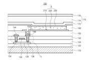
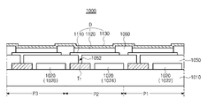
図2は、本発明の例示的な第1実施形態に係る有機発光表示装置を概略的に示す断面図である。図2に示すように、有機発光表示装置100は、基板110と、基板110の上部に位置する薄膜トランジスタTrと、平坦化層150上に位置し、薄膜トランジスタTrに接続される有機発光ダイオードDとを含む。
FIG. 2 is a schematic cross-sectional view of an organic light emitting diode display according to a first exemplary embodiment of the present invention. As shown in FIG. 2, the organic light
基板110は、ガラス基板であってもよく、薄いフレキシブルな基板であってもよく、高分子プラスチック基板であってもよい。例えば、フレキシブルな基板は、ポリイミド(PI)、ポリエーテルスルホン(PES)、ポリエチレンナフタレート(PEN)、ポリエチレンテレフタレート(PET)、およびポリカーボネート(PC)のうち、いずれか1つで形成することができる。上部に薄膜トランジスタTrと有機発光ダイオードDの位置する基板110は、アレイ基板を成す。
基板110上にバッファー層122が形成され、バッファー層122上に薄膜トランジスタTrが形成される。バッファー層122は省略してもよい。
A
バッファー層122の上部に半導体層120が形成される。例えば、半導体層120は、酸化物半導体物質から形成することができる。半導体層120が酸化物半導体物質からなる場合、半導体層120の下部に遮光パターン(不図示)を形成することができる。遮光パターンは、半導体層120へ光が入射することを防止し、半導体層120が光によって劣化することを防止する。選択的に、半導体層120は多結晶シリコンから形成することもできるが、この場合、半導体層120の両端部に不純物をドープすることもある。
A
半導体層120の上部には、絶縁物質からなるゲート絶縁膜124が基板110の全面に形成される。ゲート絶縁膜124は、シリコン酸化物(SiOx)、またはシリコン窒化物(SiNx)のような無機絶縁物質から形成することができる。
A
ゲート絶縁膜124の上部には、金属のような導電性物質からなるゲート電極130が半導体層120の中央に対応して形成される。図2において、ゲート絶縁膜124は、基板110の全面に形成されているが、ゲート絶縁膜124は、ゲート電極130と同じ形にパターニングしてもよい。
A
ゲート電極130の上部には、絶縁物質からなる層間絶縁膜132が基板110の全面に形成される。層間絶縁膜132は、シリコン酸化物(SiOx)やシリコン窒化物(SiNx)のような無機絶縁物質で形成してもよく、ベンゾシクロブテンやフォトアクリルのような有機絶縁物質で形成してもよい。
An interlayer insulating
層間絶縁膜132は、半導体層120の両側上面を露出する第1および第2半導体層コンタクトホール134、136を有する。第1および第2半導体層コンタクトホール134、136は、ゲート電極130の両側に、ゲート電極130と離隔して位置する。ここで、第1および第2半導体層コンタクトホール134、136は、ゲート絶縁膜124内にも形成することができる。ゲート絶縁膜124がゲート電極130と同じ形にパターニングされる場合、第1および第2半導体層コンタクトホール134、136は、層間絶縁膜132内にのみ形成される。
The
層間絶縁膜132の上部には、金属のような導電性物質からなるソース電極144とドレイン電極146が形成される。ソース電極144とドレイン電極146は、ゲート電極130を介在して離隔して位置し、それぞれ第1および第2半導体層コンタクトホール134、136を介して、半導体層120の両側に接触する。
A
半導体層120、ゲート電極130、ソース電極144、およびドレイン電極146は、薄膜トランジスタTrを構成し、薄膜トランジスタTrは、駆動素子として働く。図2に示した薄膜トランジスタTrは、半導体層120の上部にゲート電極130、ソース電極144およびドレイン電極146が位置するコプラナ構造を有する。あるいは、薄膜トランジスタTrは、半導体層の下部にゲート電極が位置し、半導体層の上部にソース電極とドレイン電極が位置する逆スタッガード(Inverted staggered)構造を有することができる。この場合、半導体層は、非晶質シリコンからなることができる。
The
図2に示していないが、ゲート配線GL(図1を参照)とデータ配線DL(図1を参照)が互いに交差して画素領域P(図1を参照)を定義し、ゲート配線GLとデータ配線DLに接続されるスイッチング素子Ts(図1を参照)がさらに形成される。スイッチング素子Tsは、駆動素子である薄膜トランジスタTrに接続される。また、パワー配線PL(図1を参照)がデータ配線DLと平行に離隔して形成され、1フレームの間に、駆動素子である薄膜トランジスタTrのゲート電極の電圧を一定に維持するためのストレージキャパシタCst(図1を参照)をさらに構成することができる。 Although not shown in FIG. 2, gate lines GL (see FIG. 1) and data lines DL (see FIG. 1) cross each other to define a pixel region P (see FIG. 1). A switching element Ts (see FIG. 1) connected to the wiring DL is further formed. The switching element Ts is connected to the thin film transistor Tr which is a drive element. In addition, a power line PL (see FIG. 1) is formed in parallel with the data line DL, and is separated from the data line DL, and a storage capacitor for maintaining a constant voltage of the gate electrode of the thin film transistor Tr, which is a driving element, during one frame. Cst (see FIG. 1) can be further configured.
一方、有機発光表示装置100は、有機発光ダイオードDから出射された光の一部を透過させるカラーフィルター層(不図示)を含むことができる。例えば、カラーフィルター層(不図示)は、赤色(R)、緑色(G)、青色(B)の光を透過させることができる。この場合、光を透過させる赤色、緑色および青色のカラーフィルターパターンをそれぞれの画素領域に形成することができる。カラーフィルター層(不図示)を採択することで、有機発光表示装置100は、フルカラーを具現化することができる。
Meanwhile, the organic light emitting
例示的側面において、有機発光表示装置100がボトムエミッションタイプである場合、有機発光ダイオードDに対応する層間絶縁膜132の上部に、光を透過させるカラーフィルター層(不図示)が位置することができる。また、有機発光表示装置100がトップエミッションタイプである場合、カラーフィルター層(不図示)は、有機発光ダイオードDの上部、すなわち、第2電極230の上部に位置することもできる。
In an exemplary aspect, if the organic light emitting
ソース電極144とドレイン電極146の上部には、平坦化層150を基板110の全面に形成する。平坦化層150は、その上面が平坦であり、薄膜トランジスタTrのドレイン電極146を露出するドレインコンタクトホール152を有する。ここで、ドレインコンタクトホール152は、第2半導体層コンタクトホール136の直上に形成されたものとして示しているが、第2半導体層コンタクトホール136と離隔して形成されてもよい。
A
有機発光ダイオードDは、平坦化層150上に位置し、薄膜トランジスタTrのドレイン電極146に接続される第1電極210と、第1電極210上に順次積層される発光層220および第2電極230を含む。
The organic light emitting diode D has a
第1電極210は、画素領域毎に分離して形成される。第1電極210は、陽極(アノード)であり得る。また、第1電極210は、仕事関数が比較的に大きい導電性物質、例えば、透明導電性物質(transparent conductive oxide、TCO)からなり得る。具体的に、第1電極210は、インジウム・スズ酸化物(Indium Tin Oxide、ITO)、インジウム・亜鉛酸化物(Indium Zinc Oxide、IZO)、インジウム・スズ・亜鉛酸化物(Indium Tin Zinc Oxide、ITZO)、スズ酸化物(SnO)、亜鉛酸化物(ZnO)、インジウム・銅酸化物(Indium Copper Oxide、ICO)、およびアルミニウム:酸化亜鉛(Al:ZnO、AZO)からなり得る。
The
例示的側面において、本発明の有機発光表示装置100がボトムエミッションタイプである場合、第1電極210は、透明導電性酸化物からなる単層構造を有することができる。本発明の有機発光表示装置100がトップエミッションタイプである場合は、第1電極210の下部に反射電極、または反射層をさらに形成することができる。
In an exemplary aspect, if the organic light emitting
例えば、前記反射電極、または前記反射層は、銀(Ag)、またはアルミニウム・パラジウム・銅(Aluminum Palladium Copper、APC)合金からなることができる。トップエミッションタイプである有機発光ダイオードDにおいて、第1電極210は、ITO/Ag/ITO、またはITO/APC/ITOの三層構造を有することができる。また、平坦化層150上には、第1電極210の端部を覆うバンク層160が形成される。バンク層160は、画素領域に対応し、第1電極210の中央を露出する。
For example, the reflective electrode or the reflective layer may be made of silver (Ag) or an aluminum-palladium-copper (APC) alloy. In the top emission type organic light emitting diode D, the
第1電極210上には、発光層220が形成される。1つの例示的側面において、発光層220は、発光物質層(Emitting Material Layer、EML)の単層構造を有することができる。選択的に、発光層220は、発光物質層と第1電極210との間に順次積層される正孔注入層(Hole Injection Layer、HIL)、正孔輸送層(Hole Transport Layer、HIL)、および/または電子遮断層(Electron Blocking Layer、EBL)、発光物質層と第2電極230との間に順次積層される正孔遮断層(Hole Blocking Layer、HBL)、電子輸送層(Electron Transport Layer、ETL)、および/または電子注入層(Electron Injection Layer、EIL)を含むことができる(図3、図8、図11および図14を参照)。また、発光層220を構成する発光部は1つであってもよく、2つ以上の発光部がタンデム構造を形成してもよい。
A
発光層220が形成された基板110の上部に、第2電極230が形成される。第2電極230は、表示領域の全面に位置し、仕事関数が比較的に小さい導電性物質からなり、陰極(カソード)として用いることができる。例えば、第2電極230は、アルミニウム(Al)、マグネシウム(Mg)、カルシウム(Ca)、銀(Ag)、またはこれらの合金や組み合わせのように反射特性のよい素材からなり得る。有機発光表示装置100がトップエミッションタイプである場合、第2電極230はその厚さが薄く、光透過(半透過)特性を有する。
A
第2電極230上には、外部の水分が有機発光ダイオードDへ浸透することを防ぐため、封止フィルム170(Encapsulation Film)が形成される。封止フィルム170は、第1無機絶縁層172と、有機絶縁層174と、第2無機絶縁層176の積層構造を有することができるが、これに限定されるものではない。
An
有機発光表示装置100は、外部光の反射を減らすための偏光板(不図示)をさらに含むことができる。例えば、偏光板(不図示)は円形状であり得る。有機発光表示装置100がボトムエミッションタイプである場合、偏光板は基板110の下部に位置することができる。一方、有機発光表示装置100がトップエミッションタイプである場合、偏光板は封止フィルム170の上部に位置することができる。また、トップエミッションタイプの有機発光表示装置100では、封止フィルム170、または偏光板(不図示)上にカバーウィンドウ(不図示)を取り付けることができる。このとき、基板110とカバーウィンドウ(不図示)がフレキシブルな素材からなる場合は、フレキシブル表示装置を構成することができる。
The
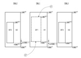
本発明の第1実施形態に係る有機発光装置に適用できる有機発光ダイオードについて具体的に説明する。図3は、本発明の第1実施形態に係る有機発光ダイオードを概略的に示す断面図である。図3に示すように、本発明の第1実施形態に係る有機発光ダイオードD1は、互いに対向する第1電極210および第2電極230と、第1電極210と第2電極230の間に位置する発光層220とを含む。有機発光表示装置100(図2を参照)は赤色の画素領域、緑色の画素領域、青色の画素領域を含み、有機発光ダイオードD1は青色の画素領域に位置することができる。
An organic light emitting diode that can be applied to the organic light emitting device according to the first embodiment of the present invention will be described in detail. FIG. 3 is a schematic cross-sectional view of an organic light emitting diode according to a first embodiment of the invention. As shown in FIG. 3, the organic light emitting diode D1 according to the first embodiment of the present invention includes a
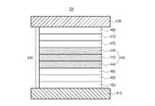
例示的側面において、発光層220は、第1電極210と第2電極230の間に位置する発光物質層240(EML)を含む。また、発光層220は、第1電極210と発光物質層240の間に位置する正孔輸送層260(HTL)と、発光物質層240と第2電極230の間に位置する電子輸送層270(ETL)のうち、少なくともいずれか1つを含むことができる。さらに、発光層220は、第1電極210と正孔輸送層260の間に位置する正孔注入層250(HIL)と、電子輸送層270と第2電極230の間に位置する電子注入層280(EIL)のうち、少なくともいずれか1つをさらに含むことができる。また、選択的に、有機発光ダイオードD1は、発光物質層240と正孔輸送層260の間に位置する電子遮断層265(EBL)、および/または発光物質層240と電子輸送層270の間に位置する正孔遮断層275(HBL)を含むことができる。
In exemplary aspects, the
第1電極210は、発光物質層240に正孔を供給する陽極であり得る。第1電極210は、仕事関数が比較的に大きい導電性物質、例えば透明導電性酸化物(TCO)から形成することが好ましい。例えば、第1電極210は、ITO、IZO、ITZO、SnO、ZnO、ICO、およびAZOからなり得る。
The
第2電極230は、発光物質層240に電子を供給する陰極であり得る。第2電極230は、仕事関数が比較的に小さい導電性物質、例えばAl、Mg、Ca、Ag、またはこれらの合金や組み合わせのように、反射特性のよい素材からなり得る。
The
発光物質層240は、第1化合物DF1(図4を参照)と第2化合物DF2(図4を参照)を含み、選択的に第3化合物H(図4を参照)を含むことができる。例えば、第1化合物DF1は第1遅延蛍光物質であり、第2化合物DF2は第2遅延蛍光物質であり、第3化合物Hはホストであり得る。
The
発光物質層240で正孔と電子が結合し、励起子を形成する際、スピンの配列により、対スピンの一重項励起子(Singlet exciton)と不対スピンの三重項励起子(Triplet exciton)が1:3の割合で生成される。従来の蛍光物質は一重項励起子だけが発光に寄与するため、発光効率が低い。一方、燐光物質は一重項励起子の他に、三重項励起子も発光に寄与するが、発光寿命が短いため、使用できるレベルには達していない。
When holes and electrons are combined to form excitons in the light-emitting
従来の蛍光物質および燐光物質が持つ短所を解決するため、第1化合物DF1および第2化合物DF2は、熱活性遅延蛍光(Thermally Activated Delayed Fluorescence、TADF)特性を有する遅延蛍光物質であり得る。遅延蛍光物質は、一重項エネルギー準位(S1 DF1、S1 DF2)と三重項エネルギー準位(T1 DF1、T1 DF2)との間のエネルギーバンドギャップ(ΔEST DF1、ΔEST DF2)が非常に狭い(図7を参照)。そのため、遅延蛍光物質であり得る第1化合物DF1および第2化合物DF2において、一重項エネルギー準位(S1 DF1、S1 DF2)を持つ励起子と三重項エネルギー準位(T1 DF1、T1 DF2)を持つ励起子は、分子内電荷移動(Intramolecular Charge Transfer、ICT)が可能な状態へ移動し(S1→ICT←T1)、そこから基底状態(S0)へ遷移する。 To overcome the disadvantages of conventional fluorescent materials and phosphorescent materials, the first compound DF1 and the second compound DF2 may be delayed fluorescent materials having thermally activated delayed fluorescence (TADF) properties. Delayed fluorophores have energy band gaps ( ΔEST DF1 , ΔEST DF2 ) between singlet energy levels (S 1 DF1 , S 1 DF2 ) and triplet energy levels ( T 1 DF1 , T 1 DF2 ). is very narrow (see Figure 7). Therefore, in the first compound DF1 and the second compound DF2, which can be delayed fluorescent substances, excitons having singlet energy levels (S 1 DF1 , S 1 DF2 ) and triplet energy levels (T 1 DF1 , T 1 DF2 ) moves to a state where intramolecular charge transfer (ICT) is possible (S 1 →ICT←T 1 ), and then transitions to the ground state (S 0 ).
遅延蛍光物質は、電子受容体部分(moiety)と電子供与体部分が分子内で離隔しているので、分子内の双極子モーメントが大きな分極状態で存在する。双極子モーメントが分極した状態で最高被占軌道(Highest Occupied Molecular Orbital、HOMO)と最低空軌道(Lowest Unoccupied Molecular Orbital、LUMO)の分子軌道間における相互作用が小さくなり、三重項状態と一重項状態からのエネルギー遷移が可能な分子内電荷移動(ICT)特性を有する。 In the delayed fluorescent substance, the electron acceptor moiety and the electron donor moiety are separated in the molecule, so that the molecule exists in a polarized state with a large intramolecular dipole moment. When the dipole moment is polarized, the interaction between the molecular orbitals of the highest occupied molecular orbital (HOMO) and the lowest unoccupied molecular orbital (LUMO) is reduced, and the triplet state and the singlet state It has intramolecular charge transfer (ICT) properties that allow energy transfer from
三重項状態と一重項状態で共にエネルギー遷移が起こるためには、遅延蛍光物質における一重項エネルギー準位(S1 DF1、S1 DF2)と三重項エネルギー準位(T1 DF1、T1 DF2)との間のエネルギーバンドギャップ(ΔEST DF1、ΔEST DF2、図7を参照)が0.3eV以下、例えば0.05eVないし0.3eVでなければならない。一重項状態と三重項状態とのエネルギー差の小さい材料は、本来の一重項状態の励起子エネルギーが基底状態へ遷移する際に蛍光を示すだけでなく、常温レベルの熱エネルギーにより、三重項状態から、エネルギーのさらに高い一重項状態へ逆項間交差(Reverse Inter System Crossing、RISC)が起こり、一重項状態の励起子が基底状態へ遷移しながら遅延蛍光を示す。 In order for energy transition to occur in both the triplet state and the singlet state, the singlet energy levels (S 1 DF1 , S 1 DF2 ) and the triplet energy levels (T 1 DF1 , T 1 DF2 ) in the delayed fluorescent substance and the energy bandgap (ΔE ST DF1 , ΔE ST DF2 , see FIG. 7) should be less than or equal to 0.3 eV, for example between 0.05 eV and 0.3 eV. A material with a small energy difference between the singlet state and the triplet state not only exhibits fluorescence when the original singlet state exciton energy transitions to the ground state, but also emits fluorescence at room temperature level thermal energy. , reverse intersystem crossing (RISC) occurs to a higher energy singlet state, and the exciton in the singlet state transits to the ground state to exhibit delayed fluorescence.
すなわち、遅延蛍光物質であり得る第1化合物DF1および第2化合物DF2において、25%の一重項エネルギー準位(S1 DF1、S1 DF2)の励起子と75%の三重項エネルギー準位(T1 DF1、T1 DF2)の励起子が、中間状態(ICT state)へ遷移し、その後、基底状態(S0)へ戻る際に発光が起こる。かかるエネルギー遷移のメカニズムにより、遅延蛍光物質の内部量子効率は、理論上100%となるので、従来の燐光物質に準ずる発光効率を達成することができる。 That is, in the first compound DF1 and the second compound DF2, which can be delayed fluorescent substances, excitons at 25% singlet energy levels (S 1 DF1 , S 1 DF2 ) and 75% triplet energy levels (T 1 DF1 , T 1 DF2 ) excitons transition to the intermediate state (ICT state) and then back to the ground state (S 0 ) to emit light. Due to such an energy transition mechanism, the internal quantum efficiency of the delayed fluorescent substance is theoretically 100%, so that it is possible to achieve a luminous efficiency equivalent to that of conventional phosphorescent substances.
本発明により、発光物質層240に含まれる第1化合物DF1は、ホウ素と酸素が縮合環を形成する遅延蛍光物質であり得る。遅延蛍光特性を有する第1化合物DF1は、下記化学式(1)で表すことができる。
According to the present invention, the first compound DF1 included in the
[化1]

化学式(1)中、R1およびR2は、それぞれ独立して、軽水素、重水素、三重水素、ボリル、置換もしくは非置換アミノ基、置換もしくは非置換C1~C20のアルキル基、置換もしくは非置換C1~C20のアルキルアミノ基、置換もしくは非置換C6~C30の芳香族基、および置換もしくは非置換C3~C30のヘテロ芳香族基で構成される群から選択される。R3ないしR6は、それぞれ独立して、軽水素、重水素、三重水素、ボリル、置換もしくは非置換C1~C20のアルキル基、置換もしくは非置換C1~C20のアルキルアミノ基、置換もしくは非置換C6~C30の芳香族基、および置換もしくは非置換C3~C30のヘテロ芳香族基で構成される群から選択されるか、またはR3ないしR6の隣接する2つが互いに結合してホウ素および酸素を有する置換もしくは非置換の縮合環を形成し、R3ないしR6の隣接する官能基のうち、少なくとも2つは互いに結合し、ホウ素および酸素を有する置換もしくは非置換の縮合環を形成する。 In chemical formula (1), R 1 and R 2 are each independently protium, deuterium, tritium, boryl, substituted or unsubstituted amino group, substituted or unsubstituted C 1 -C 20 alkyl group, substituted or selected from the group consisting of unsubstituted C 1 -C 20 alkylamino groups, substituted or unsubstituted C 6 -C 30 aromatic groups, and substituted or unsubstituted C 3 -C 30 heteroaromatic groups; be. R 3 to R 6 are each independently hydrogen, deuterium, tritium, boryl, substituted or unsubstituted C 1 -C 20 alkyl group, substituted or unsubstituted C 1 -C 20 alkylamino group, is selected from the group consisting of substituted or unsubstituted C 6 -C 30 aromatic groups and substituted or unsubstituted C 3 -C 30 heteroaromatic groups, or two adjacent R 3 to R 6 are bonded to each other to form a substituted or unsubstituted condensed ring having boron and oxygen, and among the adjacent functional groups of R 3 to R 6 , at least two are bonded to each other and substituted or unsubstituted Forms a substituted fused ring.
例えば、化学式(1)において、R1ないしR6であり得るC6~C30の芳香族基、およびC3~C30のヘテロ芳香族基は、それぞれ独立して、非置換であってもよく、C1~C10のアルキル基、C6~C30のアリール基、およびC3~C30のヘテロアリール基で構成される群から選択される少なくとも1つの官能基で置換されてもよい。 For example, in chemical formula (1), the C 6 -C 30 aromatic group and the C 3 -C 30 heteroaromatic group, which may be R 1 to R 6 , may each independently be unsubstituted optionally substituted with at least one functional group selected from the group consisting of C 1 to C 10 alkyl groups, C 6 to C 30 aryl groups, and C 3 to C 30 heteroaryl groups; .
例示的側面において、化学式(1)のR1ないしR6をそれぞれ構成することができるC6~C30の芳香族基は、C6~C30のアリール基、C7~C30のアラルキル基、C6~C30のアリールオキシ基、およびC6~C30のアリールアミノ基を含むことができるが、これに限定されるものではない。化学式(1)のR1ないしR6をそれぞれ構成することができるC3~C30のヘテロ芳香族基は、C3~C30のヘテロアリール基、C4~C30のヘテロアラルキル基、C3~C30のヘテロアリールオキシ基、およびC3~C30のヘテロアリールアミノ基を含むことができるが、これに限定されるものではない。 In an exemplary aspect, the C 6 to C 30 aromatic groups that can constitute R 1 to R 6 of Formula (1), respectively, are C 6 to C 30 aryl groups, C 7 to C 30 aralkyl groups. , C 6 -C 30 aryloxy groups, and C 6 -C 30 arylamino groups, but are not limited thereto. The C 3 to C 30 heteroaromatic group that can constitute each of R 1 to R 6 in the chemical formula (1) includes a C 3 to C 30 heteroaryl group, a C 4 to C 30 heteroaralkyl group, a C It can include, but is not limited to, C 3 -C 30 heteroaryloxy groups, and C 3 -C 30 heteroarylamino groups.
例えば、R1ないしR6をそれぞれ構成することができるC6~C30のアリール基は、フェニル、ビフェニル、ターフェニル、ナフチル、アントラセニル、ペンタレニル、インデニル、インデノインデニル、ヘプタレニル、ビフェニルレニル、インダセニル、フェナレニル、フェナントレニル、ベンゾフェナントレニル、ジベンゾフェナントレニル、アズレニル、ピレニル、フルオランテニル、トリフェニルレニル、クリセニル、テトラフェニル、テトラセニル、プレイアデニル、ピセニル、ペンタフェニル、ペンタセニル、フルオレニル、インデノフルオレニル、またはスピロフルオレニルのような、縮合または非縮合のアリール基であり得るが、これに限定されるものではない。 For example, the C 6 -C 30 aryl groups that can constitute R 1 to R 6 respectively are phenyl, biphenyl, terphenyl, naphthyl, anthracenyl, pentalenyl, indenyl, indenoindenyl, heptalenyl, biphenylenyl, indacenyl, phenalenyl, phenanthrenyl, benzophenanthrenyl, dibenzophenanthrenyl, azulenyl, pyrenyl, fluoranthenyl, triphenylenyl, chrysenyl, tetraphenyl, tetracenyl, preiadenyl, picenyl, pentaphenyl, pentacenyl, fluorenyl, It can be a fused or non-fused aryl group such as, but not limited to, indenofluorenyl, or spirofluorenyl.
選択的に、R1ないしR6をそれぞれ構成することができるC3~C30のヘテロアリール基は、ピロリル、ピリジニル、ピリミジニル、ピラジニル、ピリダジニル、トリアジニル、テトラジニル、イミダゾリル、ピラゾリル、インドリル、イソインドリル、インダゾリル、インドリジニル、ピロリジニル、カルバゾリル、ベンゾカルバゾリル、ジベンゾカルバゾリル、インドロカルバゾリル、インデノカルバゾリル、ベンゾフロカルバゾリル、ベンゾチエノカルバゾリル、キノリニル、イソキノリニル、フタラジニル、キノキサリニル、シノリニル、キナゾリニル、キノゾリニル、キノリジニル、プリニル、ベンゾキノリニル、ベンゾイソキノリニル、ベンゾキナゾリニル、ベンゾキノキサリニル、アクリジニル、フェナントロリニル、ペリミジニル、フェナントレジニル、プテリジニル、ナフタリジニル、フラニル、ピラニル、オキサジニル、オキサゾリル、オキサジアゾリル、トリアゾリル、ジオキシニル、ベンゾフラニル、ジベンゾフラニル、チオピラニル、ザンテニル、クロメニル、イソクロメニル、チオアジニル、チオフェニル、ベンゾチオフェニル、ジベンゾチオフェニル、ジフロピラジニル、ベンゾフロジベンゾフラニル、ベンゾチエノベンゾチオフェニル、ベンゾチエノジベンゾチオフェニル、ベンゾチエノベンゾフラニル、ベンゾチエノジベンゾフラニル、またはN-置換されたスピロフルオレニル、スピロフルオレノアクリジニル、スピロフルオレノザンテニルのような、縮合または非縮合のヘテロアリール基であり得るが、これに限定されるものではない。 Optionally, the C 3 -C 30 heteroaryl groups that can constitute R 1 to R 6 respectively are pyrrolyl, pyridinyl, pyrimidinyl, pyrazinyl, pyridazinyl, triazinyl, tetrazinyl, imidazolyl, pyrazolyl, indolyl, isoindolyl, indazolyl. , indolizinyl, pyrrolidinyl, carbazolyl, benzocarbazolyl, dibenzocarbazolyl, indolocarbazolyl, indenocarbazolyl, benzofurocarbazolyl, benzothienocarbazolyl, quinolinyl, isoquinolinyl, phthalazinyl, quinoxalinyl, cinolinyl , quinazolinyl, quinazolinyl, quinolidinyl, purinyl, benzoquinolinyl, benzoisoquinolinyl, benzoquinazolinyl, benzoquinoxalinyl, acridinyl, phenanthrolinyl, perimidinyl, phenantredinyl, pteridinyl, naphthalidinyl, furanyl, pyranyl, oxazinyl, oxazolyl, oxadiazolyl, triazolyl, dioxynyl, benzofuranyl, dibenzofuranyl, thiopyranyl, zanthenyl, chromenyl, isochromenyl, thioazinyl, thiophenyl, benzothiophenyl, dibenzothiophenyl, difuropyrazinyl, benzoflodibenzofuranyl, benzothienobenzothiophenyl, fused or non-fused compounds such as benzothienodibenzothiophenyl, benzothienobenzofuranyl, benzothienodibenzofuranyl, or N-substituted spirofluorenyl, spirofluorenoacridinyl, spirofluorenozantenyl; It can be, but is not limited to, a heteroaryl group.
化学式(1)中、R3ないしR6の隣接する2つの官能基は互いに結合し、ホウ素および酸素を有する縮合環を形成し、遅延蛍光特性を有する。また、ホウ素および酸素を有する縮合環構造を形成し、第1化合物DF1におけるHOMOエネルギー準位とLUMOエネルギー準位との間のエネルギーバンドギャップ(Eg)が、第2化合物DF2におけるHOMOエネルギー準位とLUMOエネルギー準位との間のエネルギーバンドギャップ(Eg)より大きくなる。したがって、第1化合物DF1から第2化合物DF2へ励起子エネルギーが移動し、超蛍光を実現することができる。 In chemical formula (1), two adjacent functional groups of R 3 to R 6 are bonded to each other to form a condensed ring containing boron and oxygen, and have delayed fluorescence properties. In addition, a condensed ring structure having boron and oxygen is formed, and the energy band gap (E g ) between the HOMO energy level and the LUMO energy level in the first compound DF1 is equal to the HOMO energy level in the second compound DF2. and the LUMO energy level (E g ). Therefore, exciton energy is transferred from the first compound DF1 to the second compound DF2, and superfluorescence can be realized.
このとき、化学式(1)中、R1およびR2、R3ないしR6の隣接する官能基が結合し、ホウ素および酸素を有する縮合環のうち、少なくとも1つ、例えば、少なくとも2つは、1つまたは2つの窒素原子を核として含む縮合ヘテロ芳香族基であり得る。例えば、かかる縮合ヘテロ芳香族基は、置換もしくは非置換カルバゾリル部分(moiety)、置換もしくは非置換アクリジニル部分、置換もしくは非置換アクリドニル部分、置換もしくは非置換フェナジニル部分、置換もしくは非置換フェノキサジニル部分、および置換もしくは非置換フェノチアジニル部分で構成される群から選択することができるが、これに限定されるものではない。 At this time, in the chemical formula (1), at least one, for example, at least two, of condensed rings having boron and oxygen, in which adjacent functional groups of R 1 and R 2 and R 3 to R 6 are bonded, It can be a fused heteroaromatic group containing one or two nitrogen atoms as a nucleus. For example, such fused heteroaromatic groups include substituted or unsubstituted carbazolyl moieties, substituted or unsubstituted acridinyl moieties, substituted or unsubstituted acridonyl moieties, substituted or unsubstituted phenazinyl moieties, substituted or unsubstituted phenoxazinyl moieties, and substituted Alternatively, it can be selected from the group consisting of unsubstituted phenothiazinyl moieties, but is not limited thereto.
例示的側面において、R1およびR2、R3ないしR6の隣接する官能基が結合し、ホウ素および酸素を有する縮合環のうち、少なくとも1つ、例えば、少なくとも2つは、他の環と縮合していないカルバゾリル基、アクリジニル基、アクリドニル基、フェナジニル基、フェノキサジニル基、およびフェノチアジニル基を含むことができる。選択的な側面において、R1およびR2、R3ないしR6の隣接する官能基が結合し、ホウ素および酸素を有する縮合環のうち、少なくとも1つ、例えば、少なくとも2つは、他の環と縮合するカルバゾリル基、アクリジニル基、アクリドニル基、フェナジニル基、フェノキサジニル基、およびフェノチアジニル基を含むことができる。このとき、これら縮合ヘテロ芳香族と縮合する他の環は、ベンゼン環、ナフタレン環、インデン環、ピリジン環、インドール環、フラン環、ベンゾフラン環、ジベンゾフラン環、チオフェン環、ベンゾチオフェン環、ジベンゾチオフェン環、および/またはこれらの組み合わせを含むことができる。 In an exemplary aspect, the adjacent functional groups of R 1 and R 2 , R 3 to R 6 are attached and at least one, such as at least two, of the condensed rings with boron and oxygen are attached to the other ring Unfused carbazolyl, acridinyl, acridonyl, phenazinyl, phenoxazinyl, and phenothiazinyl groups can be included. In optional aspects, the adjacent functional groups of R 1 and R 2 , R 3 to R 6 are attached, and of the fused rings with boron and oxygen, at least one, such as at least two, of the other rings carbazolyl, acridinyl, acridonyl, phenazinyl, phenoxazinyl, and phenothiazinyl groups fused with At this time, other rings condensed with these condensed heteroaromatics are benzene ring, naphthalene ring, indene ring, pyridine ring, indole ring, furan ring, benzofuran ring, dibenzofuran ring, thiophene ring, benzothiophene ring and dibenzothiophene ring. , and/or combinations thereof.
例えば、R1およびR2、R3ないしR6の隣接する官能基が結合し、ホウ素および酸素を有する縮合環のうち、少なくとも1つ、例えば、少なくとも2つは、インデノカルバゾリル基、インドロカルバゾリル基、ベンゾフロカルバゾリル基、および/またはベンゾチエノカルバゾリル基を含むことができるが、これに限定されるものではない。または、R1およびR2、R3ないしR6の隣接する官能基が結合し、ホウ素および酸素を有する縮合環のうち、少なくとも1つ、例えば、少なくとも2つは、他の環と共にスピロ構造を形成することができる。例えば、R1およびR2、R3ないしR6の隣接する官能基が結合してホウ素および酸素を有する縮合環のうち、少なくとも1つ、例えば、少なくとも2つは、スピロフルオレノアクリジニル基を含むことができるが、これに限定されるものではない。R1およびR2、R3ないしR6の隣接する官能基が結合し、ホウ素および酸素を有する縮合環のうち、少なくとも1つ、例えば、少なくとも2つは、非置換であってもよく、またはC1~C10のアルキル基、C6~C30のアリール基、およびC3~C30のヘテロアリール基で構成される群から選択される少なくとも1つの官能基で置換されたカルバゾリル部分、若しくはアクリジニル部分を含んでもよいが、これに限定されるものではない。
For example, at least one, for example, at least two of the condensed rings having boron and oxygen to which adjacent functional groups of R 1 and R 2 , R 3 to R 6 are bonded are indenocarbazolyl groups, It can include, but is not limited to, indolocarbazolyl, benzofurocarbazolyl, and/or benzothienocarbazolyl groups. Alternatively, at least one, for example, at least two of the condensed rings having boron and oxygen to which adjacent functional groups of R 1 and R 2 and R 3 to R 6 are bonded form a spiro structure together with other rings can be formed. For example, at least one, for example at least two, of condensed rings having boron and oxygen to which adjacent functional groups of R 1 and R 2 and R 3 to R 6 are bonded are spirofluorenoacridinyl groups can include, but is not limited to, at least one, such as at least two, of the fused rings having boron and oxygen to which the adjacent functional groups of R 1 and R 2 ,
例えば、R1ないしR6を構成する縮合ヘテロ芳香族基は、非置換であってもよく、またはC1~C10のアルキル基(例えば、t-ブチル基のようなC1~C5のアルキル基)、C6~C30のアリール基(例えば、フェニル基のようなC6~C15のアリール基)、およびC3~C30のヘテロアリール基(例えば、ピリジル基のようなC3~C15のヘテロアリール基)で構成される群から選択される少なくとも1つの官能基で置換されてもよい。 For example, the fused heteroaromatic groups comprising R 1 through R 6 may be unsubstituted or may be C 1 -C 10 alkyl groups (eg, C 1 -C 5 alkyl groups such as t-butyl groups). alkyl groups), C 6 to C 30 aryl groups (for example, C 6 to C 15 aryl groups such as phenyl groups), and C 3 to C 30 heteroaryl groups (for example, C 3 to C 15 heteroaryl group).
例示的側面において、化学式(1)中、R4とR5が互いに結合し、ホウ素および酸素を有する縮合環を形成することができる。このような構造を有する第1化合物DF1は、下記化学式(2A)、または化学式(2B)で表すことができるが、これに限定されるものではない。 In an exemplary aspect, in formula (1), R4 and R5 can be joined together to form a fused ring with boron and oxygen. The first compound DF1 having such a structure can be represented by the following chemical formula (2A) or chemical formula (2B), but is not limited thereto.
[化2A]

[化2B]

化学式(2A)および化学式(2B)中、R11ないしR15は、それぞれ独立して、軽水素、重水素、三重水素、ボリル、置換もしくは非置換アミノ基、置換もしくは非置換C1~C20のアルキル基、置換もしくは非置換C1~C20のアルキルアミノ基、置換もしくは非置換C6~C30の芳香族基、および置換もしくは非置換C3~C30のヘテロ芳香族基で構成される群から選択され、R11ないしR14のうち、少なくとも1つは、置換もしくは非置換カルバゾリル部分、置換もしくは非置換アクリジニル部分、置換もしくは非置換アクリドニル部分、置換もしくは非置換フェナジニル部分、置換もしくは非置換フェノキサジニル部分、および置換もしくは非置換フェノチアジニル部分で構成される群から選択される。 In Chemical Formula (2A) and Chemical Formula (2B), R 11 to R 15 are each independently hydrogen, deuterium, tritium, boryl, substituted or unsubstituted amino group, substituted or unsubstituted C 1 to C 20 alkyl groups, substituted or unsubstituted C 1 -C 20 alkylamino groups, substituted or unsubstituted C 6 -C 30 aromatic groups, and substituted or unsubstituted C 3 -C 30 heteroaromatic groups at least one of R 11 to R 14 is a substituted or unsubstituted carbazolyl moiety, a substituted or unsubstituted acridinyl moiety, a substituted or unsubstituted acridonyl moiety, a substituted or unsubstituted phenazinyl moiety, a substituted or unsubstituted It is selected from the group consisting of substituted phenoxazinyl moieties, and substituted or unsubstituted phenothiazinyl moieties.
例えば、化学式(2A)および化学式(2B)中、R11ないしR15であり得るC6~C30の芳香族基、およびC3~C30のヘテロ芳香族基は、それぞれ独立して、非置換であってもよく、またはC1~C10のアルキル基、C6~C30のアリール基、およびC3~C30のヘテロアリール基で構成される群から選択される少なくとも1つの官能基で置換されてもよい。また、R11ないしR14であり得るカルバゾリル部分、アクリジニル部分、アクリドニル部分、フェナジニル部分、フェノキサジニル部分、およびフェノチアジニル部分は、それぞれ独立して、非置換であってもよく、C1~C10のアルキル基、C6~C30のアリール基、C3~C30のヘテロアリール基で構成される群から選択される少なくとも1つの官能基で置換されてもよい。 For example, in Formula (2A) and Formula (2B), the C 6 -C 30 aromatic group and the C 3 -C 30 heteroaromatic group, which may be R 11 to R 15 , are each independently non- optionally substituted, or at least one functional group selected from the group consisting of C 1 -C 10 alkyl groups, C 6 -C 30 aryl groups, and C 3 -C 30 heteroaryl groups may be replaced with Also, the carbazolyl, acridinyl, acridonyl, phenazinyl, phenoxazinyl, and phenothiazinyl moieties that may be R 11 to R 14 may each independently be unsubstituted, C 1 to C 10 It may be substituted with at least one functional group selected from the group consisting of an alkyl group, a C 6 to C 30 aryl group, and a C 3 to C 30 heteroaryl group.
化学式(2A)、または化学式(2B)で表される構造を有する有機化合物は、遅延蛍光特性を有するだけでなく、後述するように、第2化合物DF2へ励起子エネルギーを効率的に移動させるに足りる一重項エネルギー準位、三重項エネルギー準位、HOMOおよびLUMOエネルギー準位を有する。例えば、化学式(2A)、または化学式(2B)で表される構造を有する第1化合物DF1は、下記化学式(3)で表される構造を有する有機化合物から選択されるいずれか1つを含むことができるが、これに限定されるものではない。 The organic compound having the structure represented by Chemical Formula (2A) or Chemical Formula (2B) not only has delayed fluorescence properties, but also has the properties of efficiently transferring exciton energy to the second compound DF2, as described later. It has sufficient singlet, triplet, HOMO and LUMO energy levels. For example, the first compound DF1 having a structure represented by chemical formula (2A) or chemical formula (2B) includes any one selected from organic compounds having a structure represented by chemical formula (3) below. can be used, but is not limited to this.
[化3]


遅延蛍光物質であり得る第1化合物DF1は、一重項エネルギー準位(S1 DF1)と三重項エネルギー準位(T1 DF1)の差(ΔEST DF1)が非常に小さく(0.3eV以下、図7を参照)、逆項間交差(RISC)によって第1化合物DF1の三重項励起子が第2化合物DF2の一重項励起子に変換されるので、量子効率に優れている。 The first compound DF1, which can be a delayed fluorescent material, has a very small difference ( ΔEST DF1 ) between the singlet energy level (S 1 DF1 ) and the triplet energy level (T 1 DF1 ) (0.3 eV or less, See FIG. 7), the triplet excitons of the first compound DF1 are converted into singlet excitons of the second compound DF2 by reverse intersystem crossing (RISC), resulting in excellent quantum efficiency.
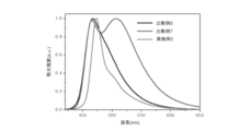
ところが、化学式(1)ないし化学式(3)で表される構造を有する第1化合物DF1は、電子供与体と電子受容体の結合により、ねじれた構造を有する。また、第1化合物DF1は、三重項励起子を利用するため、さらなる電荷移動遷移(Charge Transfer Transition、CT Transition)が引き起こされる。CT発光メカニズムに起因する発光特性により、化学式(1)ないし化学式(3)で表される構造を有する第1化合物DF1は、その半値幅(Full Width at Half Maximum、FWHM)が広く、色純度の面において限界がある。 However, the first compound DF1 having the structure represented by Chemical Formulas (1) to (3) has a twisted structure due to the bond between the electron donor and the electron acceptor. Further, since the first compound DF1 utilizes triplet excitons, a further charge transfer transition (CT transition) is induced. The first compound DF1 having the structure represented by the chemical formulas (1) to (3) has a wide full width at half maximum (FWHM) and a high color purity due to the luminous properties resulting from the CT luminescence mechanism. There are limits in terms of
また、第1化合物DF1の一重項エネルギー準位(S1
DF1)にある励起子の一部は、項間交差(Inter System Crossing、ISC)により、三重項エネルギー準位(T1
DF1)に遷移する。そして、第1化合物DF1において、RISCによって三重項エネルギー準位(T1
DF1)から一重項エネルギー準位(S1
DF1)へ遷移できず、三重項エネルギー準位(T1
DF1)に残留する三重項励起子が生成される。かかる三重項励起子は、周辺の三重項励起子、またはポーラロンと相互作用し、三重項-三重項消滅(Triplet-Triplet annhilation、TTA)または三重項-ポーラロン消滅(Triplet-Polaron annhilation 、TPA)によって消光(クエンチ)する。すなわち、発光物質層240が第1化合物DF1のみを含む場合、第1化合物DF1の三重項励起子エネルギーは発光に寄与することができない。さらに、TTAやTPAのような消光過程により、有機発光ダイオードの寿命が低下することがある。
In addition, some of the excitons at the singlet energy level (S 1 DF1 ) of the first compound DF1 transition to the triplet energy level (T 1 DF1 ) due to intersystem crossing (ISC). do. Then, in the first compound DF1, the triplet energy level (T 1 DF1 ) cannot be transitioned from the triplet energy level (
第1遅延蛍光物質である第1化合物DF1の発光特性を極大化できるよう、発光物質層240は、第2遅延蛍光物質であり得る第2化合物DF2を含み、超蛍光(Hyperfluorescence)を実現する。前述したとおり、遅延蛍光物質である第1化合物DF1および第2化合物DF2は、一重項励起子エネルギーと三重項励起子エネルギーを利用することができる。したがって、発光物質層240が、第1遅延蛍光物質である第1化合物DF1に比べ、適切なエネルギー準位を有する第2遅延蛍光物質を第2化合物DF2に含むと、第1化合物DF1から放出された励起子エネルギーを第2化合物DF2が吸収し、第2化合物DF2が吸収したエネルギーは、100%の確率で一重項励起子のみを生成し、発光効率を極大化することができる。
The
発光物質層240に含まれる第1遅延蛍光物質である第1化合物DF1の三重項励起子エネルギーからアップコンバートされた一重項励起子エネルギーと、本来の一重項励起子エネルギーを含む第1化合物DF1の一重項励起子エネルギーは、フェルスター共鳴エネルギー移動(Forster Resonance Energy Transfer、FRET)のメカニズムにより、同一の発光物質層内の第2遅延蛍光物質である第2化合物DF2へ移動し、第2化合物DF2で最終的な発光が起こる。第1化合物DF1で生成された励起子エネルギーが第2化合物DF2へ効率的に移動するよう、第1化合物DF1の発光波長帯に対する吸収波長帯の重なる部分が大きい化合物を第2化合物DF2として用いることができる。最終的に発光する第2化合物DF2は、半値幅が狭いので、色純度を向上させることができる。
The singlet exciton energy up-converted from the triplet exciton energy of the first compound DF1, which is the first delayed fluorescent material contained in the
発光物質層240に含まれる第2化合物DF2は、青色を発する遅延蛍光物質であり得る。例えば、発光物質層240に含まれる第2化合物DF2は、半値幅(FWHM)が35nm以下のホウ素系遅延蛍光物質であり得る。一例に、ホウ素系遅延蛍光物質である第2化合物DF2は、下記化学式(4)で表すことができる。
The second compound DF2 included in the
[化4]

化学式(4)中、R21ないしR24は、それぞれ独立して、軽水素、重水素、三重水素、ボリル、置換もしくは非置換アミノ基、置換もしくは非置換C1~C20のアルキル基、置換もしくは非置換C1~C20のアルキルアミノ基、置換もしくは非置換C6~C30の芳香族基、および置換もしくは非置換C3~C30のヘテロ芳香族基で構成される群から選択されるか、またはR21ないしR24の隣接する2つが互いに結合してホウ素および窒素を有する置換もしくは非置換の縮合環を形成し、R21ないしR24の隣接する官能基のうち、2つは互いに結合し、ホウ素および窒素を有する置換もしくは非置換の縮合環を形成する。また、R25ないしR28は、それぞれ独立して、軽水素、重水素、三重水素、ボリル、置換もしくは非置換C1~C20のアルキル基、置換もしくは非置換C1~C20のアルキルアミノ基、置換もしくは非置換C6~C30の芳香族基、および置換もしくは非置換C3~C30のヘテロ芳香族基で構成される群から選択される。 In chemical formula (4), R 21 to R 24 are each independently hydrogen, deuterium, tritium, boryl, substituted or unsubstituted amino group, substituted or unsubstituted C 1 -C 20 alkyl group, substituted or selected from the group consisting of unsubstituted C 1 -C 20 alkylamino groups, substituted or unsubstituted C 6 -C 30 aromatic groups, and substituted or unsubstituted C 3 -C 30 heteroaromatic groups; or two adjacent R 21 to R 24 are bonded together to form a substituted or unsubstituted condensed ring having boron and nitrogen, and two of the adjacent functional groups of R 21 to R 24 are Combined with each other to form a substituted or unsubstituted fused ring with boron and nitrogen. R 25 to R 28 each independently represent protium, deuterium, tritium, boryl, substituted or unsubstituted C 1 -C 20 alkyl group, substituted or unsubstituted C 1 -C 20 alkylamino substituted or unsubstituted C 6 -C 30 aromatic groups, and substituted or unsubstituted C 3 -C 30 heteroaromatic groups.
例えば、化学式(4)中、R21ないしR24であり得るC6~C30の芳香族基、およびC3~C30のヘテロ芳香族基は、それぞれ独立して、非置換であってもよく、またはC1~C10のアルキル基、C6~C30のアリール基、およびC3~C30のヘテロアリール基で構成される群から選択される少なくとも1つの官能基で置換されてもよい。 For example, in chemical formula (4), the C 6 -C 30 aromatic group and the C 3 -C 30 heteroaromatic group, which may be R 21 to R 24 , may each independently be unsubstituted or substituted with at least one functional group selected from the group consisting of C 1 -C 10 alkyl groups, C 6 -C 30 aryl groups, and C 3 -C 30 heteroaryl groups. good.
化学式(1)と同様に、化学式(4)のR21ないしR28を構成するC6~C30の芳香族基は、C6~C30のアリール基、C7~C30のアラルキル基、C6~C30のアリールオキシ基、およびC6~C30のアリールアミノ基を含むことができ、R21ないしR28を構成するC3~C30のヘテロ芳香族基は、C3~C30のヘテロアリール基、C4~C30のヘテロアラルキル基、C3~C30のヘテロアリールオキシ基、およびC3~C30のヘテロアリールアミノ基を含むことができるが、これに限定されるものではない。 As in chemical formula (1), the C 6 to C 30 aromatic groups constituting R 21 to R 28 in chemical formula (4) are C 6 to C 30 aryl groups, C 7 to C 30 aralkyl groups, The C 3 -C 30 heteroaromatic groups constituting R 21 to R 28 can include C 6 -C 30 aryloxy groups and C 6 -C 30 arylamino groups, and the C 3 -C 30 heteroaromatic groups constituting R 21 to R 28 are can include, but are not limited to, 30 heteroaryl groups, C 4 -C 30 heteroaralkyl groups, C 3 -C 30 heteroaryloxy groups, and C 3 -C 30 heteroarylamino groups. not a thing
化学式(4)で表される構造を有するホウ素系化合物は、発光特性に優れている。また、該化合物は広い板状構造をしているので、第1化合物DF1からの励起子エネルギー移動を効率的に受けることができ、発光効率を極大化することができる。 A boron-based compound having a structure represented by the chemical formula (4) has excellent light-emitting properties. In addition, since the compound has a broad plate-like structure, it can efficiently receive the exciton energy transfer from the first compound DF1, thereby maximizing the luminous efficiency.
例示的側面において、化学式(4)のR22とR23は互いに結合し、ホウ素および窒素を有する縮合環を形成することができる。例えば、第2化合物DF2は、下記化学式(5A)、または化学式(5B)で表される構造を有するホウ素系化合物を含むことができる。 In an exemplary aspect, R 22 and R 23 of formula (4) can be linked together to form a fused ring with boron and nitrogen. For example, the second compound DF2 can include a boron-based compound having a structure represented by the following chemical formula (5A) or chemical formula (5B).
[化5A]
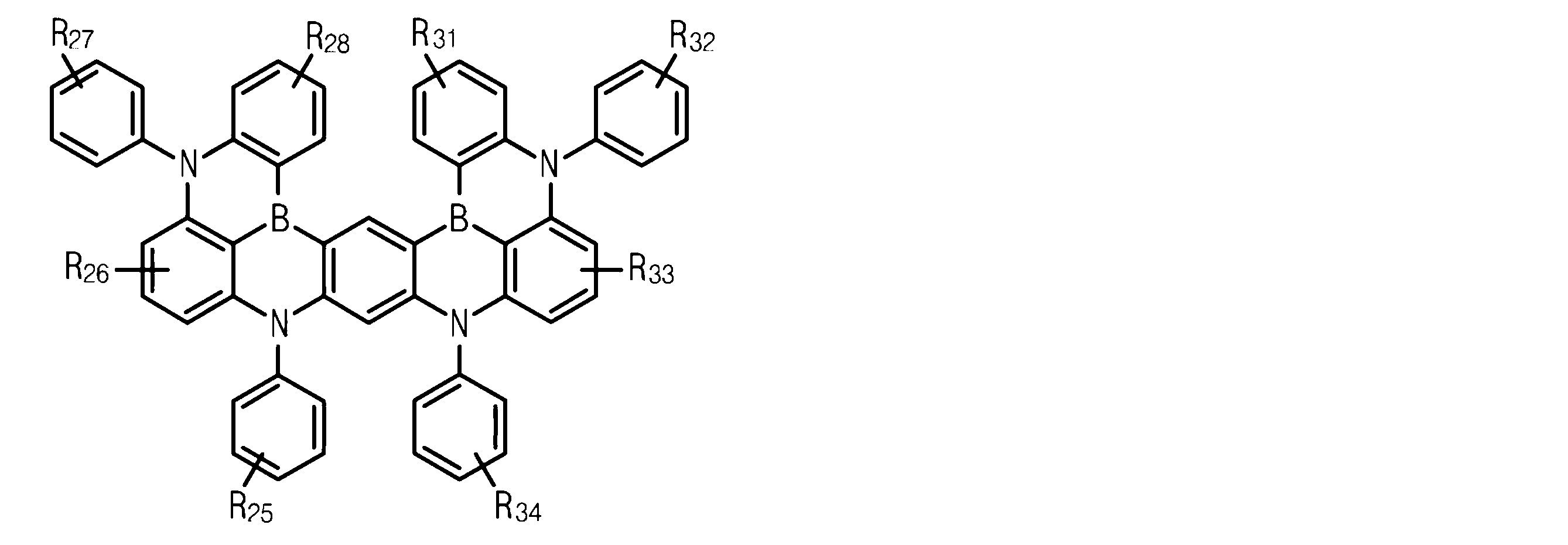
[化5B]

化学式(5A)および化学式(5B)中、R25ないしR28およびR31ないしR34は、それぞれ独立して、軽水素、重水素、三重水素、ボリル、置換もしくは非置換C1~C20のアルキル基、置換もしくは非置換C1~C20のアルキルアミノ基、置換もしくは非置換C6~C30の芳香族基、および置換もしくは非置換C3~C30のヘテロ芳香族基で構成される群から選択される。 In Chemical Formula (5A) and Chemical Formula (5B), R 25 to R 28 and R 31 to R 34 are each independently hydrogen, deuterium, tritium, boryl, substituted or unsubstituted C 1 -C 20 composed of alkyl groups, substituted or unsubstituted C 1 -C 20 alkylamino groups, substituted or unsubstituted C 6 -C 30 aromatic groups, and substituted or unsubstituted C 3 -C 30 heteroaromatic groups Selected from the group.
例えば、化学式(5A)および化学式(5B)中、R25ないしR34であり得るC6~C30の芳香族基、およびC3~C30のヘテロ芳香族基は、それぞれ独立して、非置換であってもよく、またはC1~C10のアルキル基、C6~C30のアリール基、およびC3~C30のヘテロアリール基で構成される群から選択される少なくとも1つの官能基で置換されてもよい。 For example, in Formula (5A) and Formula (5B), the C 6 -C 30 aromatic group and the C 3 -C 30 heteroaromatic group, which may be R 25 to R 34 , are each independently non- optionally substituted, or at least one functional group selected from the group consisting of C 1 -C 10 alkyl groups, C 6 -C 30 aryl groups, and C 3 -C 30 heteroaryl groups may be replaced with
他の例示的側面において、ホウ素系化合物である第2化合物DF2は、下記化学式(6)で表される構造を有する有機化合物から選択されるいずれか1つを含むことができるが、これに限定されるものではない。 In another exemplary aspect, the second compound DF2, which is a boron-based compound, may include any one selected from organic compounds having a structure represented by the following chemical formula (6), but is limited thereto: not to be
[化6]

一方、発光物質層240に含まれ得る第3化合物Hは、第1化合物DF1、および/または第2化合物DF2と比べ、HOMOエネルギー準位とLUMOエネルギー準位との間のエネルギーバンドギャップ(Eg)の広い任意の有機化合物を含むことができる。発光物質層240が、ホストであり得る第3化合物Hを含む場合、第1化合物DF1は第1ドーパントであり、第2化合物DF2は第2ドーパントであり得る。
On the other hand, the third compound H that may be included in the
例示的側面において、発光物質層240に含まれ得る第3化合物Hは、4,4’-ビス(N-カルバゾリル)-1,1’-ビフェニル;CBP、3,3’-ビス(N-カルバゾリル)-1,1’-ビフェニル;mCBP、1,3-ビス(カルバゾール-9-イル)ベンゼン;mCP、9-(3-(9H-カルバゾール-9-イル)フェニル)-9H-カルバゾール-3-カルボニトリル;mCP-CN、オキシビス(2,1-フェニレン)ビス(ジフェニルホスフィンオキシド);DPEPO、2,8-ビス(ジフェニルホスホリル)ジベンゾチオフェン;PPT、1,3,5-トリ[(3-ピリジル)-フェン-3-イル]ベンゼン;TmPyPB、2,6-ジ(9H-カルバゾール-9-イル)ピリジン;PYD-2Cz、2,8-ジ(9H-カルバゾール-9-イル)ジベンゾチオフェン;DCzDBT、3’,5’-ジ(カルバゾール-9-イル)-[1,1’-ビフェニル]-3,5-ジカルボニトリル;DCzTPA、4’-(9H-カルバゾール-9-イル)ビフェニル-3,5-ジカルボニトリル;pCzB-2CN、3’-(9H-カルバゾール-9-イル)ビフェニル-3,5-ジカルボニトリル;mCzB-2CN、ジフェニル-4-トリフェニルシリルフェニル-ホスフィンオキシド;TPS01、9-(9-フェニル-9H-カルバゾール-6-イル)-9H-カルバゾール;CCP、4-(3-(トリフェニレン-2-イル)フェニル)ジベンゾ[b,d]チオフェン、9-(4-(9H-カルバゾール-9-イル)フェニル)-9H-3,9’-ビカルバゾール、9-(3-(9H-カルバゾール-9-イル)フェニル)-9H-3,9’-ビカルバゾール、9-(6-(9H-カルバゾール-9-イル)ピリジン-3-イル)-9H-3,9’-ビカルバゾール、およびこれらの組み合わせを含むことができるが、これに限定されるものではない。 In exemplary aspects, the third compound H that may be included in the luminescent material layer 240 is 4,4′-bis(N-carbazolyl)-1,1′-biphenyl; CBP, 3,3′-bis(N-carbazolyl )-1,1′-biphenyl; mCBP, 1,3-bis(carbazol-9-yl)benzene; mCP, 9-(3-(9H-carbazol-9-yl)phenyl)-9H-carbazole-3- carbonitrile; mCP-CN, oxybis(2,1-phenylene)bis(diphenylphosphine oxide); DPEPO, 2,8-bis(diphenylphosphoryl)dibenzothiophene; PPT, 1,3,5-tri[(3-pyridyl )-phen-3-yl]benzene; TmPyPB, 2,6-di(9H-carbazol-9-yl)pyridine; PYD-2Cz, 2,8-di(9H-carbazol-9-yl)dibenzothiophene; DCzDBT , 3′,5′-di(carbazol-9-yl)-[1,1′-biphenyl]-3,5-dicarbonitrile; DCzTPA, 4′-(9H-carbazol-9-yl)biphenyl-3 ,5-dicarbonitrile; pCzB-2CN, 3′-(9H-carbazol-9-yl)biphenyl-3,5-dicarbonitrile; mCzB-2CN, diphenyl-4-triphenylsilylphenyl-phosphine oxide; TPS01 , 9-(9-phenyl-9H-carbazol-6-yl)-9H-carbazole; CCP, 4-(3-(triphenylen-2-yl)phenyl)dibenzo[b,d]thiophene, 9-(4- (9H-carbazol-9-yl)phenyl)-9H-3,9′-bicarbazole, 9-(3-(9H-carbazol-9-yl)phenyl)-9H-3,9′-bicarbazole, 9 -(6-(9H-carbazol-9-yl)pyridin-3-yl)-9H-3,9'-bicarbazole, and combinations thereof, but not limited to.
例示的側面において、発光物質層240(EML)が第1化合物DF1、第2化合物DF2、および第3化合物Hを含む場合、発光物質層240内の第3化合物Hの含有量は、第1化合物DF1の含有量より大きく、第1化合物DF1の含有量は、第2化合物DF2の含有量より大きくてもよい。第1化合物DF1の含有量が第2化合物DF2の含有量より大きい場合、第1化合物DF1から第2化合物DF2へとFRETメカニズムによる励起子エネルギー移動が十分に起こり得る。一例に、発光物質層240(EML)中、第3化合物Hは55重量%~85重量%、第1化合物DF1は10重量%~40重量%、例えば10重量%~30重量%、第2化合物DF2は0.1重量%~5重量%、例えば0.1重量%~2重量%で含むことができるが、これに限定されるものではない。
In an exemplary aspect, when the luminescent material layer 240 (EML) includes a first compound DF1, a second compound DF2, and a third compound H, the content of the third compound H in the
例示的側面において、ホストである第3化合物Hと、第1遅延蛍光物質である第1化合物DF1と、第2遅延蛍光物質である第2化合物DF2のHOMOエネルギー準位、および/またはLUMOエネルギー準位を適切に調節しなければならない。例えば、超蛍光を実現するため、ホストは、遅延蛍光物質における三重項状態の励起子が消光(非発光消滅、クエンチ)せずに発光に寄与できるよう誘導しなければならない。そのため、ホストである第3化合物H、第1遅延蛍光物質である第1化合物DF1、第2遅延蛍光物質である第2化合物DF2のエネルギー準位を調節する必要がある。 In exemplary aspects, the HOMO energy levels and/or LUMO energy levels of the host third compound H, the first delayed fluorescent material first compound DF1, and the second delayed fluorescent material second compound DF2 Position must be adjusted appropriately. For example, to achieve superfluorescence, the host must induce triplet state excitons in delayed fluorophores to contribute to emission without quenching. Therefore, it is necessary to adjust the energy levels of the third compound H that is the host, the first compound DF1 that is the first delayed fluorescent substance, and the second compound DF2 that is the second delayed fluorescent substance.
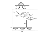
図4は、本発明の第1実施形態に係る有機発光ダイオードD1において、発光物質層を構成する第1化合物および第2化合物のエネルギー準位を調節し、電荷が効率的に移動する状態を概略的に示す模式図である。 FIG. 4 schematically shows a state in which the energy levels of the first compound and the second compound constituting the light-emitting material layer are adjusted in the organic light-emitting diode D1 according to the first embodiment of the present invention, and charges are efficiently transferred. FIG. 2 is a schematic diagram schematically showing;
図4に示すように、ホストであり得る第3化合物HのHOMOエネルギー準位(HOMOH)は、第1遅延蛍光物質であり得る第1化合物DF1のHOMOエネルギー準位(HOMODF1)より深く、第3化合物HのLUMOエネルギー準位(LUMOH)は、第1化合物DF1のLUMOエネルギー準位(LUMODF1)より浅くあり得る。言い換えると、第3化合物HのHOMOエネルギー準位(HOMOH)とLUMOエネルギー準位(LUMOH)との間のエネルギーバンドギャップは、第1化合物DF1のHOMOエネルギー準位(HOMODF1)とLUMOエネルギー準位(LUMODF1)との間のエネルギーバンドギャップより広くてよい。 As shown in FIG. 4, the HOMO energy level (HOMO H ) of the third compound H that can be the host is deeper than the HOMO energy level (HOMO DF1 ) of the first compound DF1 that can be the first delayed fluorescent substance, The LUMO energy level (LUMO H ) of the third compound H can be shallower than the LUMO energy level (LUMO DF1 ) of the first compound DF1. In other words, the energy bandgap between the HOMO energy level (HOMO H ) and the LUMO energy level (LUMO H ) of the third compound H is the same as the HOMO energy level (HOMO DF1 ) of the first compound DF1 and the LUMO energy It may be wider than the energy bandgap between the level (LUMO DF1 ).
一例に、発光物質層(EML)において、ホストであり得る第3化合物HのHOMOエネルギー準位(HOMOH)と、第1遅延蛍光物質であり得る第1化合物DF1のHOMOエネルギー準位(HOMODF1)の差(│HOMOH-HOMODF1│)、または第3化合物HのLUMOエネルギー準位(LUMOH)と、第1化合物DF1のLUMOエネルギー準位(LUMODF1)の差(│LUMOH-LUMODF1│)は、0.5eV以下、例えば0.1eV~0.5eVであり得る。この場合、第3化合物Hから第1化合物DF1への電荷移動、および/または電荷注入効率が向上し、有機発光ダイオードD1の発光効率が向上することができる。 For example, in the emissive material layer (EML), the HOMO energy level (HOMO H ) of the third compound H that may be the host and the HOMO energy level (HOMO DF1 ) difference ( |HOMO H −HOMO DF1 | ) , or the difference (|LUMO H −LUMO DF1 |) may be less than or equal to 0.5 eV, for example between 0.1 eV and 0.5 eV. In this case, the efficiency of charge transfer and/or charge injection from the third compound H to the first compound DF1 is improved, and the luminous efficiency of the organic light emitting diode D1 can be improved.
例示的側面において、第1化合物DF1のHOMOエネルギー準位(HOMODF1)と、第2化合物DF2のHOMOエネルギー準位(HOMODF2)との間のエネルギーバンドギャップ(ΔHOMO-1)は、下記式(I)を満たす。 In an exemplary aspect, the energy bandgap (ΔHOMO−1) between the HOMO energy level of the first compound DF1 (HOMO DF1 ) and the HOMO energy level of the second compound DF2 (HOMO DF2 ) is defined by the following formula ( I) is satisfied.
│HOMODF2-HOMODF1│<0.3eV…(I) │HOMO DF2 −HOMO DF1 │<0.3 eV (I)
第1化合物DF1のHOMOエネルギー準位(HOMODF1)と、第2化合物DF2のHOMOエネルギー準位(HOMODF2)との間のエネルギーバンドギャップ(ΔHOMO-1)が式(I)を満たす場合、発光物質層240へ注入された正孔は、第1化合物DF1へ移動することができる。それにより、第1化合物DF1は、本来の一重項励起子エネルギーと、RISCメカニズムにより三重項エネルギー準位から遷移した一重項励起子エネルギーを全て利用し、100%の内部量子効率を実現することができ、第2化合物DF2へ励起子エネルギーが効率的に移動することができる。例えば、第1化合物DF1のHOMOエネルギー準位(HOMODF1)と、第2化合物DF2のHOMOエネルギー準位(HOMODF2)は、下記式(II)を満たすことができるが、これに限定されるものではない。
When the energy band gap (ΔHOMO-1) between the HOMO energy level (HOMO DF1 ) of the first compound DF1 and the HOMO energy level (HOMO DF2 ) of the second compound DF2 satisfies the formula (I), light emission Holes injected into the
│HOMODF2-HOMODF1│≦0.2eV …(II) │HOMO DF2 −HOMO DF1 │≦0.2 eV (II)
他の例示的側面において、第1化合物DF1のLUMOエネルギー準位(LUMODF1)は、第2化合物DF2のLUMOエネルギー準位(LUMODF2)に比べ、浅くてもよく、同一であってもよい。例えば、第1化合物DF1のLUMOエネルギー準位(LUMODF1)と、第2化合物DF2のLUMOエネルギー準位(LUMODF2)は、下記式(III)を満たすことができる。 In other exemplary aspects, the LUMO energy level (LUMO DF1 ) of the first compound DF1 may be shallower than or the same as the LUMO energy level (LUMO DF2 ) of the second compound DF2. For example, the LUMO energy level (LUMO DF1 ) of the first compound DF1 and the LUMO energy level (LUMO DF2 ) of the second compound DF2 can satisfy the following formula (III).
0≦│LUMODF1-LUMODF2│≦0.5eV …(III) 0≦|LUMO DF1 −LUMO DF2 |≦0.5 eV (III)
第1化合物DF1のLUMOエネルギー準位(LUMODF1)と、第2化合物DF2のLUMOエネルギー準位(LUMODF2)が式(III)を満たす場合、発光物質層240へ注入された電子は、第1化合物DF1へ移動することができる。それにより、第1遅延蛍光物質である第1化合物DF1で励起子の再結合が起こり得るので、RISCメカニズムを介して100%の内部量子効率を実現することができる。第1化合物DF1でRISCを介して生成された一重項励起子エネルギーは、FRETを介して第2遅延蛍光物質である第2化合物DF2へ移動し、第2化合物DF2で効率的な発光が起こり得る。
When the LUMO energy level (LUMO DF1 ) of the first compound DF1 and the LUMO energy level (LUMO DF2 ) of the second compound DF2 satisfy formula (III), electrons injected into the light-emitting
例えば、第1化合物DF1のHOMOエネルギー準位(HOMODF1)は、-5.4eV~-5.7eVであり、第1化合物DF1のLUMOエネルギー準位(LUMODF1)は、-2.6eV~-2.9eVであり得るが、これに限定されるものではない。第2化合物DF2のHOMOエネルギー準位(HOMODF2)は、-5.3eV~-5.6eVであり、第2化合物DF2のLUMOエネルギー準位(LUMODF2)は、-2.7eV~-2.9eVであり得るが、これに限定されるものではない。 For example, the HOMO energy level (HOMO DF1 ) of the first compound DF1 is −5.4 eV to −5.7 eV, and the LUMO energy level (LUMO DF1 ) of the first compound DF1 is −2.6 eV to − It can be 2.9 eV, but is not limited to this. The HOMO energy level (HOMO DF2 ) of the second compound DF2 is −5.3 eV to −5.6 eV, and the LUMO energy level (LUMO DF2 ) of the second compound DF2 is −2.7 eV to −2. It can be 9 eV, but is not limited to this.
第1化合物DF1のHOMOエネルギー準位(HOMODF1)とLUMOエネルギー準位(LUMODF1)との間のエネルギーバンドギャップは、第2化合物DF2のHOMOエネルギー準位(HOMODF2)とLUMOエネルギー準位(LUMODF2)との間のエネルギーバンドギャップより広くてよい。例示的側面において、第1化合物DF1のHOMOエネルギー準位(HOMODF1)とLUMOエネルギー準位(LUMODF1)との間のエネルギーバンドギャップは、2.6eV以上3.1eV以下、例えば、2.7eV以上2.9eV以下であり得る。第2化合物DF2のHOMOエネルギー準位(HOMODF2)とLUMOエネルギー準位(LUMODF2)のバンドギャップは、2.4eV以上2.9eV以下、例えば、2.5eV以上2.8eV以下であり得る。この場合、第1化合物DF1で生成された励起子エネルギーが第2化合物DF2へ効率的に遷移し、最終的に第2化合物DF2で十分な発光が起こり得る。 The energy bandgap between the HOMO energy level (HOMO DF1 ) and the LUMO energy level (LUMO DF1 ) of the first compound DF1 is the same as the HOMO energy level (HOMO DF2 ) and the LUMO energy level ( LUMO DF2 ). In exemplary aspects, the energy bandgap between the HOMO energy level (HOMO DF1 ) and the LUMO energy level (LUMO DF1 ) of the first compound DF1 is greater than or equal to 2.6 eV and less than or equal to 3.1 eV, such as 2.7 eV. It can be more than or equal to 2.9 eV or less. The band gap between the HOMO energy level (HOMO DF2 ) and the LUMO energy level (LUMO DF2 ) of the second compound DF2 may be 2.4 eV or more and 2.9 eV or less, for example, 2.5 eV or more and 2.8 eV or less. In this case, the exciton energy generated in the first compound DF1 can efficiently transfer to the second compound DF2, and finally sufficient light emission can occur in the second compound DF2.
図5は、発光物質層を構成する第1化合物および第2化合物のHOMOエネルギー準位を調節していないとき、正孔が第2化合物にトラップされる問題を概略的に示す模式図である。図5に示すように、第1化合物DF1のHOMOエネルギー準位(HOMODF1)と第2化合物DF2のHOMOエネルギー準位(HOMODF2)との間のエネルギーバンドギャップ(ΔHOMO-2)が、0.3eV以上である場合、発光物質層240へ注入された正孔は、第2遅延蛍光物質である第2化合物DF2にトラップされる。すなわち、発光物質層240へ注入された正孔は、ホストである第3化合物Hから第1遅延蛍光物質である第1化合物DF1へ移動しない。発光効率に優れている第1化合物DF1で励起子が形成されず、第2化合物DF2にトラップされた正孔が直接再結合して励起子を形成し、発光する。第1化合物DF1の三重項励起子エネルギーは発光に寄与することができず、非発光消滅するため、発光効率が減少する。
FIG. 5 is a schematic diagram schematically showing the problem that holes are trapped in the second compound when the HOMO energy levels of the first compound and the second compound constituting the luminescent material layer are not adjusted. As shown in FIG. 5, the energy bandgap (ΔHOMO-2) between the HOMO energy level (HOMO DF1 ) of the first compound DF1 and the HOMO energy level (HOMO DF2 ) of the second compound DF2 is 0.5. When the voltage is 3 eV or more, holes injected into the light-emitting
図6は、発光物質層を構成する第1化合物並びに第2化合物のHOMOエネルギー準位およびLUMOエネルギー準位を調節していないとき、正孔が第2化合物にトラップされ、第1化合物と第2化合物の間に励起複合体が形成される問題を概略的に示す模式図である。図6に示すように、第1化合物DF1のHOMOエネルギー準位(HOMODF1)と第2化合物DF2のHOMOエネルギー準位(HOMODF2)との間のエネルギーバンドギャップ(ΔHOMO-3)が、0.5eV以上である場合、発光物質層240へ注入された正孔は、第2遅延蛍光物質である第2化合物DF2にトラップされる。
FIG. 6 shows that when the HOMO energy level and LUMO energy level of the first compound and the second compound constituting the light-emitting material layer are not adjusted, holes are trapped in the second compound, and the first compound and the
また、第1化合物DF1のLUMOエネルギー準位(LUMODF1)が第2化合物DF2のLUMOエネルギー準位(LUMODF2)より深い場合(すなわち、LUMODF2-LUMODF1>0である場合)、第2化合物DF2にトラップされた正孔と、第1化合物DF1へ移動した電子が励起複合体を形成する。三重項励起子エネルギーが非発光消滅し、発光効率が減少する上に、励起複合体を形成するLUMOエネルギー準位とHOMOエネルギー準位との間のエネルギーバンドギャップが非常に狭くなるため、長波長帯域の光が発光する。第1化合物DF1と第2化合物DF2が同時に発光するため、半値幅が広くなり、色純度が低下する。 Also, when the LUMO energy level (LUMO DF1 ) of the first compound DF1 is deeper than the LUMO energy level (LUMO DF2 ) of the second compound DF2 (that is, when LUMO DF2 −LUMO DF1 >0), the second compound A hole trapped in DF2 and an electron transferred to the first compound DF1 form an excitatory complex. In addition to non-radiative annihilation of triplet exciton energy and reduced luminous efficiency, the energy bandgap between the LUMO and HOMO energy levels forming the exciton complex becomes very narrow, resulting in long wavelength A band of light is emitted. Since the first compound DF1 and the second compound DF2 emit light at the same time, the half-value width widens and the color purity decreases.
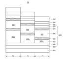
続いて、本発明の第1実施形態に係る発光物質層240における発光メカニズムについて説明する。図7は、本発明の第1実施形態に係る有機発光ダイオードを構成する発光物質層における発光物質間の一重項エネルギー準位および三重項エネルギー準位による発光メカニズムを概略的に示す模式図である。図7に概略的に示すように、発光物質層240(EML)に含まれるホストであり得る第3化合物Hの一重項エネルギー準位(S1
H)は、遅延蛍光特性を有する第1化合物DF1の一重項エネルギー準位(S1
DF1)より高い。また、第3化合物Hの三重項エネルギー準位(T1
H)は、第2化合物DF2の三重項エネルギー準位(T1
DF2)より高くあり得る。例えば、第3化合物Hの三重項エネルギー準位(T1
H)は、第1化合物DF1の三重項エネルギー準位(T1
DF1)より0.2eV以上、好ましくは0.3eV以上、さらに好ましくは0.5eV以上高くてもよい。
Next, a light emitting mechanism in the light emitting
第3化合物Hの三重項エネルギー準位(T1
H)および一重項エネルギー準位(S1
H)が、第1化合物DF1の三重項エネルギー準位(T1
DF1)および一重項エネルギー準位(S1
DF1)より十分に高くない場合、第1化合物DF1の三重項エネルギー準位(T1
DF1)の励起子が第3化合物Hの三重項エネルギー準位(T1
H)へと逆電荷移動が起こる。それにより、三重項励起子が発光できない第3化合物Hで三重項励起子は非発光消滅するため、遅延蛍光特性を有する第1化合物DF1の三重項励起子は発光に寄与できなくなる。遅延蛍光特性を有する第1化合物DF1の一重項エネルギー準位(S1
DF1)と三重項エネルギー準位(T1
DF1)の差(ΔEST
DF1)は、0.3eV以下、例えば0.05eV~0.3eVであり得る。
The triplet energy level (T 1 H ) and singlet energy level (S 1 H ) of the third compound H are equal to the triplet energy level (
また、発光物質層240(EML)において、RISCにより、ICT錯体状態に変わった第1遅延蛍光物質である第1化合物DF1から第2遅延蛍光物質である第2化合物DF2へ励起子エネルギーが効率的に遷移し、高効率、かつ高色純度を有する有機発光ダイオードD1を具現化する必要がある。かかる有機発光ダイオードD1を具現化するため、第1遅延蛍光物質であり得る第1化合物DF1の一重項エネルギー準位(S1
DF1)は、第2遅延蛍光物質であり得る第2化合物DF2の一重項エネルギー準位(S1
DF2)より高くなければならない。選択的に、第1化合物DF1の三重項エネルギー準位(T1
DF1)は、第2化合物DF2の三重項エネルギー準位(T1
DF2)より高くてもよい。
In addition, in the light-emitting material layer 240 (EML), exciton energy is efficiently transferred from the first compound DF1, which is the first delayed fluorescent material, which has changed to the ICT complex state by RISC to the second compound DF2, which is the second delayed fluorescent material. , to implement an organic light emitting diode D1 with high efficiency and high color purity. To implement such an organic light-emitting diode D1, the singlet energy level (S 1 DF1 ) of the first compound DF1, which may be the first delayed phosphor, is reduced to the singlet energy level (
一方、第2化合物DF2の一重項エネルギー準位(S1 DF2)と三重項エネルギー準位(T1 DF2)との間のエネルギーバンドギャップ(ΔEST DF2)は、第1化合物DF1の一重項エネルギー準位(S1 DF1)と三重項エネルギー準位(T1 DF1)との間のエネルギーバンドギャップ(ΔEST DF1)より小さい。そのため、FRETメカニズムを介し、第1化合物DF1の一重項エネルギー準位(S1 DF1)から第2化合物DF2の一重項エネルギー準位(S1 DF2)へ移動した励起子エネルギーが、ISCにより、三重項エネルギー準位(T1 DF2)へ変換されても、第2化合物DF2の三重項エネルギー準位(T1 DF2)の励起子は、RISCによって素早く一重項エネルギー準位(S1 DF2)へ変換する。 On the other hand, the energy bandgap (ΔE ST DF2 ) between the singlet energy level (S 1 DF2 ) and the triplet energy level (T 1 DF2 ) of the second compound DF2 is the singlet energy of the first compound DF1 less than the energy bandgap (ΔE ST DF1 ) between the level (S 1 DF1 ) and the triplet energy level (T 1 DF1 ). Therefore, the exciton energy transferred from the singlet energy level (S 1 DF1 ) of the first compound DF1 to the singlet energy level (S 1 DF2 ) of the second compound DF2 via the FRET mechanism is triplet Although converted to the term energy level (T 1 DF2 ), the excitons at the triplet energy level (T 1 DF2 ) of the second compound DF2 are quickly converted to the singlet energy level (S 1 DF2 ) by RISC. do.
その結果、第2化合物DF2に残留する三重項励起子が減少し、三重項励起子が周辺の三重項励起子、またはポーラロンと相互作用することが防止され、TTAまたはTPAによる三重項励起子の消光を最小化することができる。第2化合物DF2は、第1化合物DF1の一重項励起子エネルギーと三重項励起子エネルギーを全て発光に利用することができるので、有機発光ダイオードD1の発光効率を極大化することができる。さらに、TTAまたはTPAといった消光が最小限になり、有機発光ダイオードD1の発光寿命が大きく向上することができる。 As a result, the triplet excitons remaining in the second compound DF2 are reduced, the triplet excitons are prevented from interacting with surrounding triplet excitons or polarons, and the triplet excitons by TTA or TPA are prevented from interacting with each other. Quenching can be minimized. Since the second compound DF2 can utilize both the singlet exciton energy and the triplet exciton energy of the first compound DF1 for light emission, the luminous efficiency of the organic light emitting diode D1 can be maximized. In addition, quenching such as TTA or TPA is minimized, and the emission lifetime of the organic light emitting diode D1 can be greatly improved.
再び図3に戻ると、正孔注入層250は、第1電極210と正孔輸送層260の間に位置し、無機物である第1電極210と有機物である正孔輸送層260の間の界面特性を向上させる。1つの例示的側面において、正孔注入層250は、4,4’,4”-トリス(3-メチルフェニルアミノ)トリフェニルアミン;MTDATA、4,4’,4”-トリス(N,N-ジフェニルアミノ)トリフェニルアミン;NATA、4,4’,4”-トリス(N-(ナフタレン-1-イル)-N-フェニルアミノ)トリフェニルアミン;1T-NATA、4,4’,4”-トリス(N-(ナフタレン-2-イル)-N-フェニルアミノ)トリフェニルアミン;2T-NATA、フタロシアニン銅;CuPC、トリス(4-カルバゾイル-9-イル-フェニル)アミン;TCTA、N,N’-ジフェニル-N,N’-ビス(1-ナフチル)-1,1’-ビフェニル-4,4”-ジアミン;NPB;NPD、1,4,5,8,9,11-ヘキサアザトリフェニレンヘキサカルボニトリル(ジピラジノ[2,3-f:2’,3’-h]キノキサリン-2,3,6,7,10,11-ヘキサカルボニトリル;HAT-CN、1,3,5-トリス[4-(ジフェニルアミノ)フェニル]ベンゼン;TDAPB、ポリ(3,4-エチレンジオキシチオフェン)ポリスチレンスルホン酸;PEDOT/PSS、N-(ビフェニル-4-イル)-9,9-ジメチル-N-(4-(9-フェニル-9H-カルバゾール-3-イル)フェニル)-9H-フルオレン-2-アミン、およびこれらの組み合わせで構成される群から選択される化合物を含むことができるが、これに限定されるものではない。有機発光ダイオードD1の特性により、正孔注入層250は省略してもよい。
Returning to FIG. 3 again, the
正孔輸送層260は、正孔注入層250と発光物質層240の間に位置する。1つの例示的側面において、正孔輸送層260は、N,N’-ジフェニル-N,N’-ビス(3-メチルフェニル)-1,1’-ビフェニル-4,4’-ジアミン;TPD、NPB(NPD)、CBP、ポリ[N,N’-ビス(4-ブチルフェニル)-N,N’-ビス(フェニル)-ベンジジン];Poly-TPD、ポリ[(9,9-ジオクチルフルオレニル-2,7-ジイル)-co-(4,4’-(N-(4-sec-ブチルフェニル)ジフェニルアミン))];TFB、ジ-[4-(N,N-ジ-p-トリルアミノ)フェニル]シクロヘキサン;TAPC、3,5-ジ(9H-カルバゾール-9-イル)-N,N-ジフェニルアニリン;DCDPA、N-(ビフェニル-4-イル)-9,9-ジメチル-N-(4-(9-フェニル-9H-カルバゾール-3-イル)フェニル)-9H-フルオレン-2-アミン、N-(ビフェニル-4-イル)-N-(4-(9-フェニル-9H-カルバゾール-3-イル)フェニル)ビフェニル)-4-アミン、およびこれらの組み合わせで構成される群から選択される化合物を含むことができるが、これに限定されるものではない。
A
発光物質層240と第2電極230の間には、電子輸送層270と電子注入層280を順次積層することができる。電子輸送層270を成す素材には、高い電子移動度が求められるが、スムーズな電子輸送により、発光物質層240に電子を安定して供給する。1つの例示的な実施形態において、電子輸送層270は、オキサジアゾール系化合物、トリアゾール系化合物、フェナントロリン系化合物、ベンゾオキサゾール系化合物、ベンゾチアゾール系化合物、ベンゾイミダゾール系化合物、トリアジン系化合物のうち、いずれか1つを含むことができる。
An
より具体的に、電子輸送層270は、トリス(8-ヒドロキシキノリン)アルミニウム;Alq3、2-ビフェニル-4-イル-5-(4-t-ブチルフェニル)-1,3,4-オキサジアゾール;PBD、スピロ-PBD、リチウムキノラート;Liq、1,3,5-トリス(N-フェニルベンゾイミダゾール-2-イル)ベンゼン;TPBi、ビス(2-メチル-8-キノリノラト-N1,08)-(1,1’-ビフェニル-4-オラト)アルミニウム;BAlq、4,7-ジフェニル-1,10-フェナントロリン;Bphen、2,9-ビス(ナフタレン-2-イル)-4,7-ジフェニル-1,10-フェナントロリン;NBphen、2,9-ジメチル-4,7-ジフェニル-1,10-フェナントロリン;BCP、3-(4-ビフェニル)-4-フェニル-5-tert-ブチルフェニル-1,2,4-トリアゾール;TAZ、4-(ナフタレン-1-イル)-3,5-ジフェニル-4H-1,2,4-トリアゾール;NTAZ、1,3,5-トリス(p-ピリド-3-イル-フェニル)ベンゼン;TpPyPB、2,4,6-トリス(3’-(ピリジン-3-イル)ビフェニル-3-イル)-1,3,5-トリアジン;TmPPPyTz、ポリ[(9,9-ビス(3’-((N,N-ジメチル)-N-エチルアンモニウム)-プロピル)-2,7-フルオレン)-アルト-2,7-(9,9-ジオクチルフルオレン)];PFNBr、トリス(フェニルキノキサリン);TPQ、TSPO1、およびこれらの組み合わせで構成される群から選択される化合物を含むことができるが、これに限定されるものではない。 More specifically, the electron- transporting layer 270 is tris(8-hydroxyquinoline)aluminum; Azoles; PBD, spiro-PBD, lithium quinolate; Liq, 1,3,5-tris(N-phenylbenzimidazol-2-yl)benzene; TPBi, bis(2-methyl-8-quinolinolato-N1,08) -(1,1′-biphenyl-4-orato)aluminum; BAlq, 4,7-diphenyl-1,10-phenanthroline; Bphen, 2,9-bis(naphthalen-2-yl)-4,7-diphenyl- 1,10-phenanthroline; NBphen, 2,9-dimethyl-4,7-diphenyl-1,10-phenanthroline; BCP, 3-(4-biphenyl)-4-phenyl-5-tert-butylphenyl-1,2 ,4-triazole; TAZ, 4-(naphthalen-1-yl)-3,5-diphenyl-4H-1,2,4-triazole; NTAZ, 1,3,5-tris(p-pyrid-3-yl -phenyl)benzene; TpPyPB, 2,4,6-tris(3′-(pyridin-3-yl)biphenyl-3-yl)-1,3,5-triazine; TmPPPyTz, poly[(9,9-bis (3′-((N,N-dimethyl)-N-ethylammonium)-propyl)-2,7-fluorene)-alto-2,7-(9,9-dioctylfluorene)]; PFNBr, tris(phenyl quinoxaline); TPQ, TSPO1, and combinations thereof.
電子注入層280は、第2電極230と電子輸送層270の間に位置するが、第2電極270の特性を改善し、素子の寿命を改善することができる。1つの例示的側面において、電子注入層280の素材には、LiF、CsF、NaF、BaF2などのアルカリハライド系物質、および/またはアルカリ土金属ハライド系物質、および/またはLiq、リチウムベンゾエイト、ステアリン酸ナトリウムなどの有機金属系の物質を用いることができるが、これに限定されるものではない。
The
一方、正孔が発光物質層240を介して第2電極230側に移動し、または電子が発光物質層240を介して第1電極210側に移動した場合、有機発光ダイオードD1の発光寿命および発光効率が低下し得る。これを防止するため、本発明の例示的な第1実施形態に係る有機発光ダイオードD1は、発光物質層240に隣接する少なくとも1つの励起子遮断層を有する。
On the other hand, when holes move toward the
本発明の第1実施形態に係る有機発光ダイオードD1は、正孔輸送層260と発光物質層240の間に、電子移動を制御・防止することができる電子遮断層265を有することができる。1つの例示的側面において、電子遮断層265は、TCTA、トリス[4-(ジエチルアミノ)フェニル]アミン、N-(ビフェニル-4-イル)-9,9-ジメチル-N-(4-(9-フェニル-9H-カルバゾール-3-イル)フェニル)-9H-フルオレン-2-アミン、TAPC、MTDATA、mCP、mCBP、CuPC、N,N’-ビス[4-[ビス(3-メチルフェニル)アミノ]フェニル]-N,N’-ジフェニル-[1,1’-ビフェニル]-4,4’-ジアミン;DNTPD、TDAPB、3,6-ビス(N-カルバゾリル)-N-フェニル-カルバゾール、およびこれらの組み合わせで構成される群から選択される化合物を含むことができるが、これに限定されるものではない。
The organic light emitting diode D1 according to the first embodiment of the present invention may have an
発光物質層240と電子輸送層270の間には、第2励起子遮断層として正孔遮断層275が位置し、発光物質層240と電子輸送層270の間の正孔移動を防止する。1つの例示的側面において、正孔遮断層275の素材として、電子輸送層270に使用できるオキサジアゾール系化合物、トリアゾール系化合物、フェナントロリン系化合物、ベンゾオキサゾール系化合物、ベンゾチアゾール系化合物、ベンゾイミダゾール系化合物、トリアジン系化合物のうち、いずれか1つを用いることができる。
A
例えば、正孔遮断層275は、発光物質層240に用いられた素材に比べ、HOMOエネルギー準位の低いBCP、BAlq、Alq3、PBD、スピロ-PBD、Liq、ビス-4,6-(3,5-ジ-3-ピリジルフェニル)-2-メチルピリミジン;B3PYMPM、DPEPO、9-(6-(9H-カルバゾール-9-イル)ピリジン-3-イル)-9H-3,9’-ビカルバゾール、およびこれらの組み合わせで構成される群から選択される化合物を含むことができるが、これに限定されるものではない。
For example, the
前述した第1実施形態では、遅延蛍光特性を有する第1化合物および第2化合物が同一の発光物質層に含まれる場合を例に挙げたが、第1化合物と第2化合物は、隣接する発光物質層にそれぞれ含まれてもよい。これについて説明する。図8は、本発明の例示的な第2実施形態に係る有機発光ダイオードを概略的に示す断面図であり、図9は、本発明の第2実施形態により、発光物質層を構成する第1化合物および第2化合物のHOMOエネルギー準位を調節し、正孔が第2化合物へ効率的に移動する状態を概略的に示す模式図であり、図10は、本発明の第2実施形態に係る有機発光ダイオードを構成する発光物質層における発光物質間の一重項エネルギー準位および三重項エネルギー準位による発光メカニズムを概略的に示す模式図である。 In the above-described first embodiment, the case where the first compound and the second compound having delayed fluorescence properties are included in the same light-emitting material layer was exemplified. may be included in each layer. This will be explained. FIG. 8 is a schematic cross-sectional view of an organic light-emitting diode according to a second exemplary embodiment of the present invention, and FIG. 9 is a first organic light-emitting diode constituting a luminescent material layer according to the second exemplary embodiment of the present invention. FIG. 10 is a schematic diagram schematically showing a state in which the HOMO energy levels of a compound and a second compound are adjusted and holes are efficiently transferred to the second compound; FIG. 10 is according to the second embodiment of the present invention; FIG. 2 is a schematic diagram schematically showing a light emission mechanism due to a singlet energy level and a triplet energy level between light emitting substances in light emitting substance layers constituting an organic light emitting diode.
図8に示すように、本発明の第2実施形態に係る有機発光ダイオードD2は、互いに対向する第1電極310および第2電極330と、第1電極310と第2電極330の間に位置する発光層320とを含む。有機発光表示装置100(図2を参照)は赤色の画素領域、緑色の画素領域、青色の画素領域を含み、有機発光ダイオードD2は青色の画素領域に位置することができる。
As shown in FIG. 8, the organic light emitting diode D2 according to the second embodiment of the present invention includes a
例示的側面において、発光層320は発光物質層340を含む。発光層320は、第1電極310と発光物質層340の間に位置する正孔輸送層360と、発光物質層340と第2電極330の間に位置する電子輸送層370のうち、少なくともいずれか1つを含むことができる。また、発光層320は、第1電極310と正孔輸送層360の間に位置する正孔注入層350と、電子輸送層370と第2電極330の間に位置する電子注入層380のうち、少なくともいずれか1つをさらに含むことができる。
In an exemplary aspect,
選択的に、発光層320は、発光物質層340と正孔輸送層360の間に位置する第1励起子遮断層である電子遮断層365、および/または発光物質層340と電子輸送層370の間に位置する第2励起子遮断層である正孔遮断層375をさらに含むことができる。第1電極310、第2電極330、および発光物質層340を除いた発光層320の構成は、前述した第1実施形態と同様であってもよい。
Optionally, light-emitting
発光物質層340は、電子遮断層365と正孔遮断層375の間に位置する第1発光物質層342(EML1、下部発光物質層、第1層)と、第1発光物質層342と正孔遮断層375の間に位置する第2発光物質層344(EML2、上部発光物質層、第2層)を含む。選択的に、第2発光物質層344は、電子遮断層365と第1発光物質層342の間に位置してもよい。
The
第1発光物質層342(EML1)と第2発光物質層344(EML2)のうち、どちらか一方は、第1遅延蛍光物質である第1化合物DF1(第1ドーパント)を含み、他方は、第2遅延蛍光物質である第2化合物DF2(第2ドーパント)を含む。また、第1発光層342(EML1)と第2発光物質層344(EML2)は、それぞれ第1ホストであり得る第4化合物H1と、第2ホストであり得る第5化合物H2を含むことができる。一例に、第1発光物質層342は第1化合物DF1を含み、第2発光物質層344は第2化合物DF2を含むことができる。
One of the first luminescent material layer 342 (EML1) and the second luminescent material layer 344 (EML2) contains the first compound DF1 (first dopant) that is the first delayed fluorescent material, and the other 2 contains a second compound DF2 (second dopant) which is a delayed fluorescent material. Also, the first light emitting layer 342 (EML1) and the second light emitting material layer 344 (EML2) may each include a fourth compound H1 that may be a first host and a fifth compound H2 that may be a second host. . For example, the first
第1発光物質層342(EML1)を構成する第1化合物DF1は、化学式(1)ないし化学式(3)で表される構造を有する第1遅延蛍光物質であり得る。遅延蛍光特性を有する第1化合物DF1は、RISCにより、第1化合物DF1の三重項励起子エネルギーが一重項励起子エネルギーに変換される。第1化合物DF1は高い量子効率を持つが、半値幅が広いため、色純度がよくない。 The first compound DF1 constituting the first light emitting material layer 342 (EML1) may be a first delayed fluorescent material having a structure represented by Chemical Formulas (1) to (3). In the first compound DF1 having delayed fluorescence properties, triplet exciton energy of the first compound DF1 is converted into singlet exciton energy by RISC. Although the first compound DF1 has a high quantum efficiency, it has a wide half-value width and thus poor color purity.
一方、第2発光物質層344(EML2)は、第2遅延蛍光物質である第2化合物DF2を含む。第2化合物DF2は、化学式(4)ないし化学式(6)で表される構造を有する任意の有機化合物を含む。化学式(4)ないし化学式(6)で表される構造を有する第2遅延蛍光物質である第2化合物DF2は、第1化合物DF1に比べ、半値幅が狭い(例えば、半値幅は35nm以下)。そのため、第2化合物DF2は、色純度の面で長所がある。 Meanwhile, the second luminescent material layer 344 (EML2) includes a second compound DF2, which is a second delayed fluorescent material. The second compound DF2 includes any organic compound having a structure represented by chemical formulas (4) to (6). The second compound DF2, which is the second delayed fluorescent material having a structure represented by chemical formulas (4) to (6), has a narrower half-value width than the first compound DF1 (for example, the half-value width is 35 nm or less). Therefore, the second compound DF2 has an advantage in terms of color purity.
本実施形態によると、第1発光物質層342(EML1)に含まれる遅延蛍光特性を有する第1化合物DF1の一重項励起子エネルギーおよび三重項励起子エネルギーは、FRETメカニズムを介し、隣接する第2発光物質層344(EML2)に含まれる第2化合物DF2へ移動し、最終的に第2化合物DF2で発光が起こる。 According to the present embodiment, the singlet exciton energy and triplet exciton energy of the first compound DF1 having delayed fluorescence properties contained in the first light-emitting material layer 342 (EML1) are transferred via the FRET mechanism to the adjacent second It migrates to the second compound DF2 contained in the luminescent material layer 344 (EML2) and finally emits light from the second compound DF2.
逆項間交差により、第1発光物質層342(EML1)に含まれる第1化合物DF1の三重項励起子エネルギーが、一重項励起子エネルギーに変換される。第1化合物DF1の一重項励起子エネルギーは、第2化合物DF2の一重項エネルギー準位に移動する。第2発光物質層344(EML2)に含まれる第2化合物DF2は、一重項励起子エネルギーと三重項励起子エネルギーを全て発光に有効利用する。 The reverse intersystem crossing converts the triplet exciton energy of the first compound DF1 contained in the first luminescent material layer 342 (EML1) into singlet exciton energy. The singlet exciton energy of the first compound DF1 is transferred to the singlet energy level of the second compound DF2. The second compound DF2 contained in the second luminescent material layer 344 (EML2) effectively utilizes both singlet exciton energy and triplet exciton energy for light emission.
第2化合物DF2の一重項エネルギー準位(S1 DF2)と三重項エネルギー準位(T1 DF2)との間のエネルギーバンドギャップ(ΔEST DF2)は、第1化合物DF1の一重項エネルギー準位(S1 DF1)と三重項エネルギー準位(T1 DF1)との間のエネルギーバンドギャップ(ΔEST DF1)より小さい(図7を参照)。第2化合物DF2の三重項エネルギー準位(T1 DF2)の励起子が、RISCにより素早く一重項エネルギー準位(S1 DF2)へ遷移することで、有機発光ダイオードD2の駆動電圧が低下し、発光効率および発光寿命が大きく向上することができる。 The energy bandgap ( ΔEST DF2 ) between the singlet energy level (S 1 DF2 ) and the triplet energy level (T 1 DF2 ) of the second compound DF2 is the singlet energy level of the first compound DF1 smaller than the energy bandgap ( ΔE ST DF1 ) between (S 1 DF1 ) and the triplet energy level (T 1 DF1 ) (see FIG . 7). Excitons at the triplet energy level (T 1 DF2 ) of the second compound DF2 quickly transition to the singlet energy level (S 1 DF2 ) by RISC, thereby reducing the driving voltage of the organic light-emitting diode D2, Luminous efficiency and luminous life can be greatly improved.
第1発光物質層342(EML1)に含まれる第1遅延蛍光物質であり得る第1化合物DF1で生成された励起子エネルギーは、第2発光物質層344(EML2)に含まれる第2遅延蛍光物質であり得る第2化合物DF2へ効率的に移動し、超蛍光を実現することができる。このとき、実質的な発光は、第2遅延蛍光物質である第2化合物DF2を含む第2発光物質層344(EML2)で起こる。その結果、有機発光ダイオードD2の量子効率が向上し、半値幅が狭くなり、色純度が向上する。 The exciton energy generated in the first compound DF1, which may be the first delayed fluorescent material contained in the first luminescent material layer 342 (EML1), is generated by the second delayed fluorescent material contained in the second luminescent material layer 344 (EML2). can efficiently migrate to a second compound DF2, which can be , and achieve superfluorescence. At this time, substantial light emission occurs in the second luminescent material layer 344 (EML2) containing the second compound DF2, which is the second delayed fluorescent material. As a result, the quantum efficiency of the organic light emitting diode D2 is improved, the half width is narrowed, and the color purity is improved.
前述した通り、第1遅延蛍光物質である第1化合物DF1は、化学式(1)ないし化学式(3)で表される構造を有する有機化合物を含み、第2遅延蛍光物質である第2化合物DF2は、化学式(4)ないし化学式(6)で表される構造を有するホウ素系化合物を含む。第4化合物H1と第5化合物H2は、互いに同一であってもよく、異なってもよい。例えば、第4化合物H1と第5化合物H2は、それぞれ独立して、第1実施形態で説明した第3化合物Hを含むことができるが、これに限定されるものではない。 As described above, the first compound DF1, which is the first delayed fluorescent substance, contains an organic compound having a structure represented by chemical formulas (1) to (3), and the second compound DF2, which is the second delayed fluorescent substance, is , and boron-based compounds having structures represented by chemical formulas (4) to (6). The fourth compound H1 and the fifth compound H2 may be the same or different. For example, the fourth compound H1 and the fifth compound H2 can independently contain the third compound H described in the first embodiment, but are not limited to this.
第1実施形態と同様に、第1化合物DF1のHOMOエネルギー準位(HOMODF1)と第2化合物DF2のHOMOエネルギー準位(HOMODF2)との間のエネルギーバンドギャップ(ΔHOMO-1)は、前述した式(I)または式(II)を満たすことができる。そのため、発光物質層340に注入された正孔は第1化合物DF1へ移動し、第1化合物DF1は、一重項励起子エネルギーと三重項励起子エネルギーを全て第2化合物DF2へ移動させることができる。また、第1化合物DF1のLUMOエネルギー準位(LUMODF1)は、第2化合物DF2のLUMOエネルギー準位(LUMODF2)より浅く、または同一であって、式(III)を満たすことができる。
As in the first embodiment, the energy bandgap (ΔHOMO-1) between the HOMO energy level (HOMO DF1 ) of the first compound DF1 and the HOMO energy level (HOMO DF2 ) of the second compound DF2 is can satisfy formula (I) or formula (II). Therefore, the holes injected into the light-emitting
さらに、第4化合物H1および第5化合物H2のHOMOエネルギー準位(HOMOH1、HOMOH2)と、第1化合物DF1のHOMOエネルギー準位(HOMODF1)の差(|HOMOH-HOMODF1|)、または第4化合物H1および第5化合物H2のLUMOエネルギー準位(LUMOH1、LUMOH2)と、第1化合物DF1のLUMOエネルギー準位(LUMODF1)の差(|LUMOH-LUMODF1|)は、0.5eV以下であり得る。かかる条件を満たさない場合、第1化合物DF1で非発光消滅が起こったり、または第4化合物H1および第5化合物H2から第1化合物DF1および/または第2化合物DF2へと励起子エネルギーが移動せず、有機発光ダイオードD2の量子効率が低下し得る。 Furthermore, the difference (|HOMO H -HOMO DF1 |) between the HOMO energy levels (HOMO H1 , HOMO H2 ) of the fourth compound H1 and the fifth compound H2 and the HOMO energy level ( HOMO DF1 ) of the first compound DF1, Or the difference (| LUMO H −LUMO DF1 |) between the LUMO energy levels (LUMO H1 , LUMO H2 ) of the fourth compound H1 and the fifth compound H2 and the LUMO energy level (LUMO DF1 ) of the first compound DF1 is It can be 0.5 eV or less. If such conditions are not satisfied, non-radiative annihilation occurs in the first compound DF1, or exciton energy is not transferred from the fourth compound H1 and the fifth compound H2 to the first compound DF1 and/or the second compound DF2. , the quantum efficiency of the organic light emitting diode D2 may be reduced.
一方、第1発光物質層342(EML1)および第2発光物質層344(EML2)にそれぞれ含まれ得る第4化合物H1および第5化合物H2でそれぞれ生成された励起子エネルギーは、まず、第1遅延蛍光物質であり得る第1化合物DF1へ移動しなければならない。図10に示すように、第4化合物H1および第5化合物H2の一重項エネルギー準位(S1 H1、S1 H2)は、それぞれ第1遅延蛍光物質であり得る第1化合物DF1の一重項エネルギー準位(S1 DF1)より高い。また、第4化合物H1および第5化合物H2の三重項エネルギー準位(T1 H1、T1 H2)は、第1化合物DF1の三重項エネルギー準位(T1 DF1)より高くあり得る。例えば、第4化合物H1および第5化合物H2の三重項エネルギー準位(T1 H1、T1 H2)は、第1化合物DF1の三重項エネルギー準位(T1 DF1)より少なくとも0.2eV以上、例えば0.3eV以上、好ましくは0.5eV以上高くてもよい。 On the other hand, the exciton energies generated in the fourth compound H1 and the fifth compound H2, respectively, which can be contained in the first luminescent material layer 342 (EML1) and the second luminescent material layer 344 (EML2), respectively, are first delayed It has to move to the first compound DF1, which can be a fluorescent substance. As shown in FIG. 10, the singlet energy levels (S 1 H1 , S 1 H2 ) of the fourth compound H1 and the fifth compound H2 are the singlet energies of the first compound DF1, which can be the first delayed fluorescent material, respectively. higher than the level (S 1 DF1 ). Also, the triplet energy levels (T 1 H1 , T 1 H2 ) of the fourth compound H1 and the fifth compound H2 may be higher than the triplet energy level (T 1 DF1 ) of the first compound DF1. For example, the triplet energy levels (T 1 H1 , T 1 H2 ) of the fourth compound H1 and the fifth compound H2 are at least 0.2 eV higher than the triplet energy level (T 1 DF1 ) of the first compound DF1, For example, it may be 0.3 eV or higher, preferably 0.5 eV or higher.
一方、第2ホストである第5化合物H2の一重項エネルギー準位(S1 H2)は、第2遅延蛍光物質である第2化合物DF2の一重項エネルギー準位(S1 DF2)より高い。選択的に、第5化合物H2の三重項エネルギー準位(T1 H2)は、第2化合物DF2の三重項エネルギー準位(T1 DF2)より高くてもよい。その結果、第5化合物H2で生成された一重項励起子エネルギーが第2化合物DF2の一重項エネルギー準位へ移動することができる。 On the other hand, the singlet energy level (S 1 H2 ) of the fifth compound H2, which is the second host, is higher than the singlet energy level (S 1 DF2 ) of the second compound DF2, which is the second delayed fluorescent material. Alternatively, the triplet energy level (T 1 H2 ) of the fifth compound H2 may be higher than the triplet energy level (T 1 DF2 ) of the second compound DF2. As a result, the singlet exciton energy generated in the fifth compound H2 can be transferred to the singlet energy level of the second compound DF2.
さらに、第1発光物質層342(EML1)でRISCにより、ICT錯体状態へ変わった第1化合物DF1から第2発光物質層344(EML2)の第2化合物DF2へ励起子エネルギーが効率的に移動しなければならない。かかる有機発光ダイオードD2を具現化するため、第1発光物質層342(EML1)に含まれる第1遅延蛍光物質である第1化合物DF1の一重項エネルギー準位(S1 DF1)は、第2発光物質層344(EML2)に含まれる第2遅延蛍光物質である第2化合物DF2の一重項エネルギー準位(S1 DF2)より高い。選択的に、第1化合物DF1の三重項エネルギー準位(T1 DF1)は、第2化合物DF2の三重項エネルギー準位(T1 DF2)より高くてもよい。 Furthermore, the exciton energy is efficiently transferred from the first compound DF1 changed to the ICT complex state by RISC in the first light-emitting material layer 342 (EML1) to the second compound DF2 in the second light-emitting material layer 344 (EML2). There must be. To implement such an organic light-emitting diode D2, the singlet energy level (S 1 DF1 ) of the first compound DF1, which is the first delayed fluorescent material contained in the first luminescent material layer 342 (EML1), is adjusted to the second emission It is higher than the singlet energy level (S 1 DF2 ) of the second compound DF2, which is the second delayed fluorescent material included in the material layer 344 (EML2). Alternatively, the triplet energy level (T 1 DF1 ) of the first compound DF1 may be higher than the triplet energy level (T 1 DF2 ) of the second compound DF2.
第1発光物質層342および第2発光物質層344のそれぞれにおいて、第4化合物H1と第5化合物H2は、それぞれ同一の発光物質層を構成する第1化合物DF1と第2化合物DF2より大きい、または同一の含有量で含むことができる。また、第1発光物質層342(EML1)に含まれる第1化合物DF1の含有量は、第2発光物質層344(EML2)に含まれる第2化合物DF2の含有量より大きくてもよい。その結果、第1発光物質層342(EML1)に含まれる第1化合物DF1から第2発光物質層344(EML2)に含まれる第2化合物DF2へと、FRETによる十分なエネルギー移動が起こり得る。
In each of the first
例えば、第1発光物質層342(EML1)中、第1化合物DF1は、1重量%~50重量%、好ましくは10重量%~40重量%、さらに好ましくは20重量%~40重量%の割合で含むことができる。第2発光物質層344(EML2)中、第2化合物DF2は、1重量%~10重量%、好ましくは1重量%~5重量%であり得る。 For example, in the first light emitting material layer 342 (EML1), the first compound DF1 is 1 wt% to 50 wt%, preferably 10 wt% to 40 wt%, more preferably 20 wt% to 40 wt%. can contain. In the second luminescent material layer 344 (EML2), the second compound DF2 may be 1 wt% to 10 wt%, preferably 1 wt% to 5 wt%.
選択的に、第2発光物質層344(EML2)が正孔遮断層375に隣接して位置する場合、第2発光物質層344(EML2)を構成する第5化合物H2は、正孔遮断層375と同一の物質であり得る。このとき、第2発光物質層344(EML2)は、発光機能と共に正孔遮断機能を備えることができる。言い換えると、第2発光物質層344(EML2)は、正孔を遮断するためのバッファー層として機能する。一方、正孔遮断層375は省略してもよく、この場合、第2発光物質層344(EML2)は、発光物質層および正孔遮断層として用いられる。
Optionally, when the second luminescent material layer 344 (EML2) is located adjacent to the
他の例示的側面において、第2発光物質層344(EML2)が電子遮断層365に隣接して位置する場合、第2発光物質層344(EML2)を構成する第5化合物H2は、電子遮断層365と同一の物質であり得る。このとき、第2発光物質層344(EML2)は、発光機能と共に電子遮断機能を備えることができる。言い換えると、第2発光物質層344(EML2)は、電子を遮断するためのバッファー層として機能する。一方、電子遮断層365は省略してもよく、この場合、第2発光物質層344(EML2)は、発光物質層および電子遮断層として用いられる。
In another exemplary aspect, when the second luminescent material layer 344 (EML2) is located adjacent to the
続いて、発光物質層が3層構造である有機発光ダイオードについて説明する。図11は、本発明の例示的な第3実施形態に係る有機発光ダイオードを概略的に示す断面図である。図12は、本発明の第3実施形態により、発光物質層を構成する第1化合物および第2化合物のHOMOエネルギー準位を調節し、正孔が第2化合物へ効率的に移動する状態を概略的に示す模式図である。図13は、本発明の第3実施形態に係る有機発光ダイオードを構成する発光物質層における発光物質間の一重項エネルギー準位および三重項エネルギー準位による発光メカニズムを概略的に示す模式図である。 Next, an organic light emitting diode having a three-layer structure of light emitting material layers will be described. FIG. 11 is a schematic cross-sectional view of an organic light emitting diode according to a third exemplary embodiment of the invention. FIG. 12 schematically shows a state in which holes are efficiently transferred to the second compound by adjusting the HOMO energy levels of the first compound and the second compound constituting the light-emitting material layer according to the third embodiment of the present invention. FIG. 2 is a schematic diagram schematically showing; FIG. 13 is a schematic diagram schematically showing a light emission mechanism due to a singlet energy level and a triplet energy level between light emitting substances in the light emitting substance layer constituting the organic light emitting diode according to the third embodiment of the present invention. .
図11に示すように、本発明の第3実施形態に係る有機発光ダイオードD3は、互いに対向する第1電極410および第2電極430と、第1電極410と第2電極430の間に位置する発光層420とを含む。有機発光表示装置100(図2を参照)は赤色の画素領域、緑色の画素領域、青色の画素領域を含み、有機発光ダイオードD3は青色の画素領域に位置することができる。
As shown in FIG. 11, the organic light emitting diode D3 according to the third embodiment of the present invention has a
本実施形態において、発光層420は3層構造の発光物質層440を含む。発光層420は、第1電極410と発光物質層440の間に位置する正孔輸送層460と、発光物質層440と第2電極430の間に位置する電子輸送層470のうち、少なくともいずれか1つを含むことができる。また、発光層420は、第1電極410と正孔輸送層460の間に位置する正孔注入層450と、電子輸送層470と第2電極430の間に位置する電子注入層480のうち、少なくともいずれか1つをさらに含むことができる。選択的に、発光層420は、発光物質層440と正孔輸送層460の間に位置する第1励起子遮断層である電子遮断層465、および/または発光物質層440と電子輸送層470の間に位置する第2励起子遮断層である正孔遮断層475をさらに含むことができる。第1電極410、第2電極430、および発光物質層440を除いた発光層420の構成は、前述した第1実施形態および第2実施形態と実質的に同様であり得る。
In this embodiment, the
発光物質層440(EML)は、電子遮断層465と正孔遮断層475の間に位置する第1発光物質層442(EML1、中間発光物質層、第1層)と、電子遮断層465と第1発光物質層442(EML1)の間に位置する第2発光物質層444(EML2、下部発光物質層、第2層)と、第1発光物質層442(EML1)と正孔遮断層475の間に位置する第3発光物質層446(EML3、上部発光物質層、第3層)を含む。
The luminescent material layer 440 (EML) includes a first luminescent material layer 442 (EML1, intermediate luminescent material layer, first layer) located between the
第1発光物質層442(EML1)は、第1遅延蛍光物質である第1化合物DF1(第1ドーパント)を含み、第2発光物質層444と第3発光物質層446は、それぞれ第2遅延蛍光物質であり得る第2化合物DF2(第2ドーパント)、および第3遅延蛍光物質であり得る第6化合物DF3(第3ドーパント)を含む。第1ないし第3発光物質層442、444、446は、それぞれ第1ホストないし第3ホストであり得る第4化合物H1、第5化合物H2および第7化合物H3をさらに含むことができる。
The first luminescent material layer 442 (EML1) contains a first compound DF1 (first dopant) that is a first delayed fluorescent material, and the second
本実施形態によると、第1発光物質層442(EML1)に含まれる第1遅延蛍光物質である第1化合物DF1の一重項励起子エネルギーおよび三重項励起子エネルギーは、フェルスター共鳴エネルギー移動(FRET)のメカニズムにより、隣接する第2発光物質層444(EML2)および第3発光物質層446(EML3)にそれぞれ含まれる第2遅延蛍光物質である第2化合物DF2、そして第3遅延蛍光物質である第6化合物DF3へ移動し、第2化合物DF2および第6化合物DF3で最終的な発光が起こる。 According to the present embodiment, the singlet exciton energy and triplet exciton energy of the first compound DF1, which is the first delayed fluorescent material contained in the first luminescent material layer 442 (EML1), are obtained by Förster resonance energy transfer (FRET ), the second compound DF2, which is the second delayed fluorescent material, and the third compound DF2, which is contained in the adjacent second luminescent material layer 444 (EML2) and the third luminescent material layer 446 (EML3), respectively, and the third delayed fluorescent material It migrates to the sixth compound DF3 and the final luminescence occurs in the second compound DF2 and the sixth compound DF3.
逆項間交差により、第1発光物質層442(EML1)に含まれる第1化合物DF1の三重項励起子エネルギーが一重項励起子エネルギーに変換される。第1遅延蛍光物質である第1化合物DF1の一重項エネルギー準位は、隣接する第2発光物質層444および第3発光物質層446にそれぞれ含まれる第2遅延蛍光物質である第2化合物DF2、および第3遅延蛍光物質である第6化合物DF3の一重項エネルギー準位より高い。第1発光物質層442(EML1)に含まれる第1化合物DF1の一重項励起子エネルギーは、FRETを介し、隣接する第2発光物質層444(EML2)および第3発光物質層446(EML3)に含まれる第2化合物DF2および第6化合物DF3の一重項エネルギー準位に移動する。
The reverse intersystem crossing converts the triplet exciton energy of the first compound DF1 contained in the first luminescent material layer 442 (EML1) into the singlet exciton energy. The singlet energy level of the first compound DF1, which is the first delayed fluorescent material, is the second compound DF2, which is the second delayed fluorescent material contained in the adjacent second
したがって、第2発光物質層444(EML2)および第3発光物質層446(EML3)にそれぞれ含まれる第2化合物DF2および第6化合物DF3は、一重項励起子エネルギーと三重項励起子エネルギーを全て発光に有効利用する。第2化合物DF2および第6化合物DF3は、第1化合物DF1に比べて半値幅が狭い(例えば、半値幅は35nm以下)。そのため、有機発光ダイオードD3の量子効率が向上し、半値幅が狭くなり、色純度が向上する。このとき、実質的な発光は、第2化合物DF2および第6化合物DF3をそれぞれ含む第2発光物質層442(EML2)および第3発光物質層446(EML3)で起こる。 Therefore, the second compound DF2 and the sixth compound DF3 contained in the second luminescent material layer 444 (EML2) and the third luminescent material layer 446 (EML3), respectively, emit all the singlet exciton energy and the triplet exciton energy. effective use for The second compound DF2 and the sixth compound DF3 have a narrower half-value width than the first compound DF1 (for example, the half-value width is 35 nm or less). Therefore, the quantum efficiency of the organic light-emitting diode D3 is improved, the half width is narrowed, and the color purity is improved. At this time, substantial light emission occurs in the second luminescent material layer 442 (EML2) and the third luminescent material layer 446 (EML3) containing the second compound DF2 and the sixth compound DF3, respectively.
第2化合物DF2および第6化合物DF3の一重項エネルギー準位(S1 DF2、S1 DF3)と三重項エネルギー準位(T1 DF2)との間のエネルギーバンドギャップ(ΔEST DF2)は、第1化合物DF1の一重項エネルギー準位(S1 DF1)と三重項エネルギー準位(T1 DF1)との間のエネルギーバンドギャップ(ΔEST DF1)より小さい(図7を参照)。第2化合物DF2および第6化合物DF3の三重項エネルギー準位(T1 DF2、T1 DF3)の励起子が、RISCにより素早く一重項エネルギー準位(S1 DF2)へ遷移することで、有機発光ダイオードD3の駆動電圧が低下し、発光効率および発光寿命が大きく向上することができる。 The energy band gap (ΔE ST DF2 ) between the singlet energy levels (S 1 DF2 , S 1 DF3 ) and the triplet energy level (T 1 DF2 ) of the second compound DF2 and the sixth compound DF3 is 1 less than the energy bandgap (ΔE ST DF1 ) between the singlet energy level (S 1 DF1 ) and the triplet energy level (T 1 DF1 ) of compound DF1 (see FIG . 7). Excitons at the triplet energy levels (T 1 DF2 , T 1 DF3 ) of the second compound DF2 and the sixth compound DF3 quickly transition to the singlet energy level (S 1 DF2 ) by RISC, resulting in organic light emission. The driving voltage of the diode D3 is lowered, and the luminous efficiency and luminous life can be greatly improved.
第1遅延蛍光物質である第1化合物DF1は、化学式(1)ないし化学式(3)で表される構造を有する有機化合物を含み、第2遅延蛍光物質である第2化合物DF2と第3遅延蛍光物質である第6化合物DF3は、それぞれ独立して、化学式(4)ないし化学式(6)で表される構造を有するホウ素系有機化合物を含む。一例に、第6化合物DF3は第2化合物DF2を含むことができる。第4化合物H1、第5化合物H2、および第7化合物H3は、互いに同一であってもよく、異なってもよい。例えば、第4化合物H1、第5化合物H2、および第7化合物H3は、それぞれ独立して、第1実施形態で説明した第3化合物Hを含むことができるが、これに限定されるものではない。 The first compound DF1, which is the first delayed fluorescent substance, contains an organic compound having a structure represented by chemical formulas (1) to (3), and the second compound DF2, which is the second delayed fluorescent substance, and the third delayed fluorescent substance The sixth compound DF3, which is a substance, independently includes a boron-based organic compound having a structure represented by chemical formulas (4) to (6). In one example, the sixth compound DF3 can include the second compound DF2. The fourth compound H1, the fifth compound H2, and the seventh compound H3 may be the same or different. For example, the fourth compound H1, the fifth compound H2, and the seventh compound H3 can each independently contain the third compound H described in the first embodiment, but are not limited thereto. .
前述した第1および第2実施形態と同様に、第1化合物DF1のHOMOエネルギー準位(HOMODF1)と、第2化合物DF2および第6化合物DF3のそれぞれのHOMOエネルギー準位(HOMODF2、HOMODF3)との間のエネルギーバンドギャップ(ΔHOMO-1)は、前述した式(I)または式(II)を満たすことができる。そのため、発光物質層340に注入された正孔は第1化合物DF1へ移動し、第1化合物DF1は、一重項励起子エネルギーと三重項励起子エネルギーを全て第2化合物DF2および第6化合物DF3へ移動させることができる。また、第1化合物DF1のLUMOエネルギー準位(LUMODF1)は、第2化合物DF2および第6化合物DF3のLUMOエネルギー準位(LUMODF2、LUMODF3)より浅く、または同一であって、式(III)を満たすことができる。
As in the first and second embodiments described above, the HOMO energy level of the first compound DF1 (HOMO DF1 ) and the HOMO energy levels of the second compound DF2 and the sixth compound DF3 (HOMO DF2 , HOMO DF3 ) can satisfy formula (I) or formula (II) described above. Therefore, the holes injected into the light emitting
さらに、第4化合物H1、第5化合物H2、および第7化合物H3のHOMOエネルギー準位(HOMOH1、HOMOH2、HOMOH3)と、第1化合物DF1のHOMOエネルギー準位(HOMODF1)の差(|HOMOH-HOMODF1|)、または第4化合物H1、第5化合物H2、および第7化合物H3のLUMOエネルギー準位(LUMOH1、LUMOH2、LUMOH3)と、第1化合物DF1のLUMOエネルギー準位(LUMODF1)の差(|LUMOH-LUMODF1|)は、0.5eV以下であり得る。 Furthermore, the difference between the HOMO energy levels (HOMO H1 , HOMO H2 , HOMO H3 ) of the fourth compound H1, the fifth compound H2, and the seventh compound H3 and the HOMO energy level (HOMO DF1 ) of the first compound DF1 ( |HOMO H -HOMO DF1 |), or the LUMO energy levels of the fourth compound H1, the fifth compound H2, and the seventh compound H3 (LUMO H1 , LUMO H2 , LUMO H3 ) and the LUMO energy level of the first compound DF1 The difference in position (LUMO DF1 ) (|LUMO H −LUMO DF1 |) may be 0.5 eV or less.
効率的は発光を実現するため、第1ないし第3発光物質層442、444、446(EML1、EML2、EML3)に含まれる発光物質のエネルギー準位を適切に調節する必要がある。図13を参照すると、第1ホストであり得る第4化合物H1の一重項エネルギー準位(S1 H1)、第2ホストであり得る第5化合物H2の一重項エネルギー準位(S1 H2)、および第3ホストであり得る第7化合物H3の一重項エネルギー準位(S1 H3)は、第1遅延蛍光物質であり得る第1化合物DF1の一重項エネルギー準位(S1 DF1)より高い。また、第4化合物H1の三重項エネルギー準位(T1 H1)、第5化合物H2の三重項エネルギー準位(T1 H2)、および第7化合物H3の三重項エネルギー準位(T1 H3)は、それぞれ第1化合物DF1の三重項エネルギー準位(T1 DF1)より高い。 In order to achieve efficient light emission, the energy levels of the luminescent materials included in the first to third luminescent material layers 442, 444 and 446 (EML1, EML2 and EML3) should be properly adjusted. Referring to FIG. 13, the singlet energy level (S 1 H1 ) of the fourth compound H1 that may be the first host, the singlet energy level (S 1 H2 ) of the fifth compound H2 that may be the second host, and the singlet energy level (S 1 H3 ) of the seventh compound H3, which may be the third host, is higher than the singlet energy level (S 1 DF1 ) of the first compound DF1, which may be the first delayed fluorescent material. Also, the triplet energy level (T 1 H1 ) of the fourth compound H1, the triplet energy level (T 1 H2 ) of the fifth compound H2 , and the triplet energy level (T 1 H3 ) of the seventh compound H3 are respectively higher than the triplet energy level (T 1 DF1 ) of the first compound DF1.
第1発光物質層442(EML1)でRISCにより、ICT錯体状態へ変わった第1化合物DF1から第2発光物質層444(EML2)および第3発光物質層446(EML3)にそれぞれ含まれる第2遅延蛍光物質である第2化合物DF2および第3遅延蛍光物質である第6化合物DF3へ励起子エネルギーが効率的に移動しなければならない。かかる有機発光ダイオードD3を具現化するため、第1発光物質層442(EML1)に含まれる第1遅延蛍光物質である第1化合物DF1の一重項エネルギー準位(S1 DF1)は、それぞれ第2発光物質層444(EML2)および第3発光物質層446(EML3)に含まれる第2遅延蛍光物質であり得る第2化合物DF2および第3遅延蛍光物質であり得る第6化合物DF3の一重項エネルギー準位(S1 DF2、S1 DF3)より高い。選択的に、第1化合物DF1の三重項エネルギー準位(T1 DF1)は、それぞれ第2化合物DF2および第6化合物DF3の三重項エネルギー準位(T1 DF2、T1 DF3)より高くてもよい。 A second retardation contained in the second luminescent material layer 444 (EML2) and the third luminescent material layer 446 (EML3), respectively, from the first compound DF1 converted to the ICT complex state by RISC in the first luminescent material layer 442 (EML1) Exciton energy must be efficiently transferred to the second compound DF2, which is a fluorescent substance, and the sixth compound DF3, which is a third delayed fluorescent substance. In order to implement such an organic light emitting diode D3, the singlet energy levels (S 1 DF1 ) of the first compound DF1, which is the first delayed fluorescent material contained in the first luminescent material layer 442 (EML1), each have a second The singlet energy levels of the second compound DF2, which may be the second delayed fluorescent material, and the sixth compound DF3, which may be the third delayed fluorescent material, contained in the luminescent material layer 444 (EML2) and the third luminescent material layer 446 (EML3) higher than the order (S 1 DF2 , S 1 DF3 ). Optionally, the triplet energy level (T 1 DF1 ) of the first compound DF1 may be higher than the triplet energy levels (T 1 DF2 , T 1 DF3 ) of the second compound DF2 and the sixth compound DF3, respectively. good.
また、第1遅延蛍光物質である第1化合物DF1から第2および第3遅延蛍光物質へ遷移したエネルギーが、第5化合物H2および第7化合物H3へ遷移することを防止し、効率的な発光を実現する必要がある。そのため、第2ホストであり得る第5化合物H2および第3ホストであり得る第7化合物H3の一重項エネルギー準位(S1 H2、S1 H3)は、それぞれ第2遅延蛍光物質であり得る第2化合物DF2および第3遅延蛍光物質であり得る第6化合物DF3の一重項エネルギー準位(S1 DF2、S1 DF3)より高くなっている。選択的に、第5化合物H2および第7化合物H3の三重項エネルギー準位(T1 H2、T1 H3)は、それぞれ第2化合物DF2および第6化合物DF3の三重項エネルギー準位(T1 DF2、T1 DF3)より高くてもよい。 In addition, the energy transitioned from the first compound DF1, which is the first delayed fluorescent substance, to the second and third delayed fluorescent substances is prevented from transitioning to the fifth compound H2 and the seventh compound H3, and efficient light emission is achieved. It is necessary to realize. Therefore, the singlet energy levels (S 1 H2 , S 1 H3 ) of the fifth compound H2 that can be the second host and the seventh compound H3 that can be the third host are the second It is higher than the singlet energy levels (S 1 DF2 , S 1 DF3 ) of the second compound DF2 and the sixth compound DF3, which may be the third delayed fluorescent substance. Optionally, the triplet energy levels (T 1 H2 , T 1 H3 ) of the fifth compound H2 and the seventh compound H3 are equal to the triplet energy levels (T 1 DF2 , T 1 DF3 ).
第1発光物質層442(EML1)に含まれる第1化合物DF1は、第2発光物質層444(EML2)および第3発光物質層446(EML3)にそれぞれ含まれる第2化合物DF2および第6化合物DF3より大きい含有量で含むことができる。この場合、第1発光物質層442(EML1)に含まれる第1化合物DF1から、第2発光物質層444(EML2)および第3発光物質層446(EML3)にそれぞれ含まれる第2化合物DF2および第6化合物DF3へと、FRETによる十分なエネルギー移動が起こり得る。 The first compound DF1 contained in the first light-emitting material layer 442 (EML1) is the second compound DF2 and the sixth compound DF3 contained in the second light-emitting material layer 444 (EML2) and the third light-emitting material layer 446 (EML3), respectively. can be included in a greater content. In this case, from the first compound DF1 contained in the first light-emitting material layer 442 (EML1) to the second compound DF2 and the second compound contained in the second light-emitting material layer 444 (EML2) and the third light-emitting material layer 446 (EML3), respectively. Sufficient energy transfer by FRET can occur to the 6-compound DF3.
例えば、第1発光物質層442(EML1)中、第1化合物DF1は、1重量%~50重量%、好ましくは10重量%~40重量%、さらに好ましくは20重量%~40重量%の割合で含むことができる。第2発光物質層444(EML2)および第3発光物質層446(EML3)のそれぞれにおいて、第2化合物DF2および第6化合物DF3は、それぞれ1重量%~10重量%、好ましくは1重量%~5重量%であり得る。 For example, in the first light emitting material layer 442 (EML1), the first compound DF1 is 1 wt% to 50 wt%, preferably 10 wt% to 40 wt%, more preferably 20 wt% to 40 wt%. can contain. In each of the second luminescent material layer 444 (EML2) and the third luminescent material layer 446 (EML3), the second compound DF2 and the sixth compound DF3 each contain 1% to 10% by weight, preferably 1% to 5% by weight. % by weight.
選択的に、第2発光物質層444(EML2)が電子遮断層465に隣接して位置する場合、第2発光物質層444(EML2)を構成する第5化合物H2は、電子遮断層465と同一の物質であり得る。このとき、第2発光物質層444(EML2)は、発光機能と共に電子遮断機能を備えることができる。言い換えると、第2発光物質層444(EML2)は、電子を遮断するためのバッファー層として機能する。一方、電子遮断層465は省略してもよく、この場合、第2発光物質層444(EML2)は、発光物質層および電子遮断層として用いられる。
Optionally, when the second luminescent material layer 444 (EML2) is positioned adjacent to the
また、第3発光物質層446(EML3)が正孔遮断層475に隣接して位置する場合、第3発光物質層446(EML3)を構成する第7化合物H3は、正孔遮断層475と同一の物質であり得る。このとき、第3発光物質層446(EML3)は、発光機能と共に正孔遮断機能を備えることができる。言い換えると、第3発光物質層446(EML3)は、正孔を遮断するためのバッファー層として機能する。一方、正孔遮断層475は省略してもよく、この場合、第3発光物質層446(EML3)は、発光物質層および正孔遮断層として用いられる。
In addition, when the third light emitting material layer 446 (EML3) is positioned adjacent to the
他の例示的側面において、第2発光物質層444(EML2)を構成する第5化合物H2は、電子遮断層465と同一の物質であり、第3発光物質層446(EML3)を構成する第7化合物H3は、正孔遮断層475と同一の物質であり得る。このとき、第2発光物質層444(EML2)は発光機能と共に電子遮断機能を備え、第3発光物質層446(EML3)は発光機能と共に正孔遮断機能を備えることができる。すなわち、第2発光物質層444(EML2)および第3発光物質層446(EML3)は、それぞれ電子と正孔を遮断するバッファー層として機能することができる。一方、電子遮断層465および正孔遮断層475は省略してもよく、この場合、第2発光物質層444(EML2)は発光物質層および電子遮断層として用いられ、第3発光物質層446(EML3)は発光物質層および正孔遮断層として用いられる。
In another exemplary aspect, the fifth compound H2 comprising the second luminescent material layer 444 (EML2) is the same material as the
選択的な実施形態において、有機発光ダイオードは、2つ以上の発光部を含むことができる。図14は、本発明の例示的な第4実施形態に係る有機発光ダイオードを概略的に示す断面図である。 In alternative embodiments, the organic light emitting diode can include more than one light emitting portion. FIG. 14 is a schematic cross-sectional view of an organic light emitting diode according to a fourth exemplary embodiment of the invention.
図14に示すように、有機発光ダイオードD4は、互いに対向する第1電極510および第2電極530と、第1電極510と第2電極530の間に位置する発光層520とを含む。有機発光表示装置100(図2を参照)は赤色の画素領域、緑色の画素領域、青色の画素領域を含み、有機発光ダイオードD4は青色の画素領域に位置することができる。また、第1電極510は陽極であり、第2電極530は陰極であり得る。
As shown in FIG. 14, the organic light emitting diode D4 includes a
発光層520は、第1発光物質層640を含む第1発光部620と、第2発光物質層740を含む第2発光部720を含む。また、発光層520は、第1発光部620と第2発光部720の間に位置する電荷発生層680をさらに含むことができる。
The
電荷発生層680は、第1発光部620と第2発光部720の間に位置し、第1電極510上に第1発光部620、電荷発生層680、第2発光部720が順次積層される。すなわち、第1発光部620は第1電極510と電荷発生層680の間に位置し、第2発光部720は第2電極530と電荷発生層680の間に位置する。
The
第1発光部620は第1発光物質層640(EML1)を含む。また、第1発光部620は、第1電極510と第1発光物質層640の間に位置する正孔注入層650(HIL)、第1発光物質層640と正孔注入層650の間に位置する第1正孔輸送層660(HTL1)と、第1発光物質層640と電荷発生層680の間に位置する第1電子輸送層670(ETL1)のうち、少なくとも1つをさらに含むことができる。選択的に、第1発光部620は、第1正孔輸送層660と第1発光物質層640の間に位置する第1電子遮断層665(EBL1)と、第1発光物質層640と第1電子輸送層670の間に位置する第1正孔遮断層675(HBL1)のうち、少なくとも1つをさらに含むことができる。
The first
第2発光部720は第2発光物質層740(EML2)を含む。また、第2発光部720は、電荷発生層680と第2発光物質層740の間に位置する第2正孔輸送層760(HTL2)、第2発光物質層740と第2電極530の間に位置する第2電子輸送層770(ETL2)と、第2電子輸送層770と第2電極530の間に位置する電子注入層780(HIL)のうち、少なくとも1つをさらに含むことができる。選択的に、第2発光部720は、第2正孔輸送層760と第2発光物質層740の間に位置する第2電子遮断層765(EBL2)と、第2発光物質層740と第2電子輸送層770の間に位置する第2正孔遮断層775(HBL2)のうち、少なくとも1つをさらに含むことができる。
The second
電荷発生層680は、第1発光部620と第2発光部720の間に位置する。言い換えると、第1発光部620と第2発光部720は、電荷発生層680を介して接続される。電荷発生層680は、N型電荷発生層682とP型電荷発生層684が接合されたPN型であり得る。
The
N型電荷発生層682は、第1電子輸送層670と第2正孔輸送層760の間に位置し、P型電荷発生層684は、N型電荷発生層682と第2正孔輸送層760の間に位置する。N型電荷発生層682は、電子を第1発光部620の第1発光物質層640へ伝達し、P型電荷発生層684は、正孔を第2発光部720の第2発光物質層740へ伝達する。
The N-type
本実施形態において、第1発光物質層640と第2発光物質層740は、それぞれ青色発光物質層であり得る。例えば、第1発光物質層640と第2発光物質層740のうち、少なくとも一方は、第1遅延蛍光物質である第1化合物DF1と、第2遅延蛍光物質である第2化合物DF2を含み、選択的に、ホストである第3化合物Hを含むことができる。
In this embodiment, the first light emitting
一例に、第1発光物質層640における第3化合物Hの含有量は、第1化合物DF1の含有量より大きく、第1化合物DF1の含有量は、第2化合物DF2の含有量より大きくてもよい。第1化合物DF1の含有量が第2化合物DF2の含有量より大きい場合、第1化合物DF1から第2化合物DF2へと、十分なエネルギー移動が起こり得る。例えば、第1発光物質層640中、第3化合物Hは55重量%~85重量%、第1化合物DF1は10重量%~40重量%、第2化合物DF2は0.1重量%~5重量%であり得るが、これに限定されるものではない。
For example, the content of the third compound H in the first light-emitting
第2発光物質層740は、第1発光物質層640と同様に第1化合物DF1および第2化合物DF2を含み、選択的に第3化合物Hを含むことができる。あるいは、第2発光物質層740は、第1発光物質層640に含まれる第1化合物DF1と第2化合物DF2のうち、少なくとも一方とは異なる別の化合物を含み、第1発光物質層640とは異なる波長の光を発するか、または異なる発光効率を有することができる。
The second
図14において、第1発光物質層640および第2発光物質層740は、単層構造であるが、第1化合物ないし第3化合物をそれぞれ含むことができる第1発光物質層640および第2発光物質層740は、それぞれ二層(図8を参照)であってもよく、三層(図11を参照)であってもよい。
In FIG. 14, the first light-emitting
本実施形態に係る有機発光ダイオードD4では、第1遅延蛍光物質である第1化合物DF1の一重項励起子エネルギーが、第2遅延蛍光物質である第2化合物DF2へ移動し、第2化合物DF2で最終的な発光が起こる。その結果、有機発光ダイオードD4の発光効率および色純度が向上する。また、化学式(1)ないし化学式(3)で表される構造を有する第1化合物DF1と、化学式(4)ないし化学式(6)で表される構造を有する第2化合物DF2が、少なくとも第1発光物質層640に用いられることで、有機発光ダイオードD4の発光効率および色純度がさらに向上する。さらに、有機発光ダイオードD4が青色発光物質層の二重積層構造を有することから、有機発光ダイオードD4の色純度が向上し、発光効率が最適化され得る。
In the organic light-emitting diode D4 according to the present embodiment, the singlet exciton energy of the first compound DF1, which is the first delayed fluorescent substance, moves to the second compound DF2, which is the second delayed fluorescent substance, and the second compound DF2 A final luminescence occurs. As a result, the luminous efficiency and color purity of the organic light emitting diode D4 are improved. Further, the first compound DF1 having the structure represented by the chemical formulas (1) to (3) and the second compound DF2 having the structure represented by the chemical formulas (4) to (6) are combined at least for the first emission The
図15は、本発明の第2実施形態に係る有機発光表示装置を概略的に示す断面図である。図15に示すように、有機発光表示装置800は、第1ないし第3画素領域P1、P2、P3が正義された基板810と、基板810の上部に位置する薄膜トランジスタTrと、薄膜トランジスタTrの上部に位置し、薄膜トランジスタTrに接続される有機発光ダイオードDとを含む。例えば、第1画素領域P1は青色の画素領域であり、第2画素領域P2は緑色の画素領域であり、第3画素領域P3は赤色の画素領域であり得る。
FIG. 15 is a schematic cross-sectional view of an organic light emitting diode display according to a second embodiment of the present invention. As shown in FIG. 15, the organic light emitting
基板810は、ガラス基板であってもよく、フレキシブル基板であってもよい。例えば、フレキシブル基板は、PI基板、PES基板、PEN基板、PET基板、およびPC基板のいずれか1つであり得る。
The
基板810上にはバッファー層812が形成され、バッファー層812上に薄膜トランジスタTrが形成されるが、バッファー層812を省略してもよい。図2を用いて説明したように、薄膜トランジスタTrは、半導体層、ゲート電極、ソース電極およびドレイン電極を含み、駆動素子として働く。
A
薄膜トランジスタTr上には平坦化層850が位置する。平坦化層850はその上面が平坦であり、薄膜トランジスタTrのドレイン電極を露出するドレインコンタクトホール852を有する。
A
有機発光ダイオードDは平坦化層850上に位置し、薄膜トランジスタTrのドレイン電極に接続される第1電極910、第1電極910上に順次積層される発光層920および第2電極930を含む。有機発光ダイオードDは、第1ないし第3画素領域P1、P2、P3にそれぞれ位置し、互いに異なる色の光を発する。例えば、第1画素領域P1の有機発光ダイオードDは青色光を発し、第2画素領域P2の有機発光ダイオードDは緑色光を発し、第3画素領域P3の有機発光ダイオードDは赤色光を発することができる。
The organic light emitting diode D is located on the
第1電極910は、第1ないし第3画素領域P1、P2、P3毎に分離して形成され、第2電極930は、第1ないし第3画素領域P1、P2、P3に対応して一体に形成される。
The
第1電極910は陽極と陰極のうち、どちらか一方であり、第2電極930は他方であり得る。また、第1電極910と第2電極930のうち、どちらか一方は透過電極(または半透過電極)であり、他方は反射電極であり得る。
The
例えば、第1電極910は陽極であり、仕事関数が比較的に大きい導電性物質、例えば透明導電性酸化物(TCO)からなる透明導電性酸化物層を含むことができる。第2電極930は陰極であり、仕事関数が比較的に小さい導電性物質、例えば低抵抗金属からなる金属物質層を含むことができる。一例に、第1電極910は、ITO、IZO、ITZO、SnO、ZnO、ICOおよびAZOのうち、いずれか1つを含み、第2電極930は、Al、Mg、Ca、Ag、またはこれらの合金(例えば、Mg-Ag合金)やこれらの組み合わせからなり得る。
For example, the
有機発光表示装置800がボトムエミッションタイプである場合、第1電極910は、透明導電性酸化物層の単層構造を有することができる。
If the organic light emitting
一方、有機発光表示装置800がトップエミッションタイプである場合、第1電極910の下部には反射電極、または反射層をさらに形成することができる。例えば、反射電極または反射層は、銀、またはアルミニウム・パラジウム・銅(APC)合金からなることができる。トップエミッションタイプである有機発光ダイオードDにおいて、第1電極910は、ITO/Ag/ITO、またはITO/APC/ITOの三層構造を有することができる。また、第2電極930はその厚さが薄く、光透過(半透過)特性を有することができる。
On the other hand, if the organic light emitting
平坦化層850上には、第1電極910の端部を覆うバンク層860が形成される。バンク層860は、第1ないし第3画素領域P1、P2、P3のそれぞれに対応し、第1電極910の中央を露出する。
A
第1電極910上には、発光層920が形成される。発光層920は、発光物質層(EML)の単層構造を有することができる。あるいは、発光層920は、発光物質層と第1電極910との間に順次積層される正孔注入層(HIL)、正孔輸送層(HTL)、および/または電子遮断層(EBL)、発光物質層と第2電極930との間に順次積層される正孔遮断層(HBL)、電子輸送層(ETL)、電子注入層(EIL)、および/または電荷発生層(Charge Generation Layer、CGL)のうち、少なくとも1つを含むことができる。
A
青色の画素領域である第1画素領域P1において、発光層920を構成する発光物質層は、化学式(1)ないし化学式(3)で表される構造を有する第1遅延蛍光物質である第1化合物DF1と、化学式(4)ないし化学式(6)で表される構造を有する第2遅延蛍光物質である第2化合物DF2を含み、選択的に、ホストである第3化合物Hを含むことができる。
In the first pixel region P1, which is the blue pixel region, the light-emitting material layer forming the light-emitting
第2電極930上には、外部の水分が有機発光ダイオードDへ浸透することを防止するため、防止フィルム870が形成される。防止フィルム870は、第1無機絶縁層、有機絶縁層、第2無機絶縁層の三層構造を有することができるが、これに限定されるものではない。
A
有機発光表示装置800は、外部光の反射を低減するための偏光板(不図示)をさらに含むことができる。例えば、偏光板(不図示)は円形状であり得る。有機発光表示装置800がボトムエミッションタイプである場合、偏光板は基板810の下部に位置することができる。一方、有機発光表示装置800がトップエミッションタイプである場合、偏光板は封止フィルム870の上部に位置することができる。
The
図16は、本発明の例示的な第5実施形態に係る有機発光ダイオードを概略的に示す断面図である。有機発光ダイオードD5は、第1電極910および第2電極930、第1電極910と第2電極930の間に位置する発光層920を含む。
FIG. 16 is a schematic cross-sectional view of an organic light emitting diode according to a fifth exemplary embodiment of the invention. The organic light emitting diode D5 includes a
第1電極910は陽極であり、第2電極930は陰極であり得る。例えば、第1電極910は反射電極であり、第2電極930は透過電極(半透過電極)であり得る。
The
発光層920は発光物質層940を含む。また、発光層920は、第1電極910と発光物質層940の間に位置する正孔輸送層960(HTL)と、発光物質層940と第2電極930の間に位置する電子輸送層970(ETL)のうち、少なくともいずれか1つを含むことができる。また、発光層920は、第1電極910と正孔輸送層960の間に位置する正孔注入層950(HIL)と、電子輸送層970と第2電極930の間に位置する電子注入層980(EIL)のうち、少なくともいずれか1つをさらに含むことができる。選択的に、発光層920は、正孔輸送層960と発光物質層940の間に位置する電子遮断層965(EBL)と、発光物質層940と電子輸送層970の間に位置する正孔遮断層975(HBL)のうち、少なくとも1つをさらに含むことができる。
さらに、発光層920は、正孔輸送層960と電子遮断層965の間に位置する補助正孔輸送層962をさらに含むことができる。補助正孔輸送層962は、第1画素領域P1に位置する第1補助正孔輸送層962a、第2画素領域P2に位置する第2補助正孔輸送層962b、および第3画素領域P3に位置する第3補助正孔輸送層962cを含むことができる。
Additionally, the light-emitting
第1補助正孔輸送層962aは第1厚さを有し、第2補助正孔輸送層962bは第2厚さを有し、第3補助正孔輸送層962cは第3厚さを有する。このとき、第1厚さは第2厚さより小さく、第2厚さは第3厚さより小さい。それにより、有機発光ダイオードD5はマイクロキャビティ構造を持つ。
The first auxiliary hole-
すなわち、第1ないし第3補助正孔輸送層962a、962b、962cの厚さが互いに異なり、第1波長範囲の光(青色)を発する第1画素領域P1における第1電極910と第2電極930間の距離は、第1波長範囲より長い第2波長範囲の光(緑色)を発する第2画素領域P2における第1電極910と第2電極930間の距離より小さい。また、第2画素領域P2における第1電極910と第2電極930間の距離は、第2波長範囲より長い第3波長範囲の光(赤色)を発する第3画素領域P3における第1電極910と第2電極930間の距離より大きい。それにより、有機発光ダイオードD5の発光効率が向上する。
That is, the thicknesses of the first through third auxiliary
図16において、第1画素領域P1に第1補助正孔輸送層962aが形成されているが、第1補助正孔輸送層962aがなくてもマイクロキャビティ構造を実現することができる。また、第2電極930上には、光取り出し向上のためのキャッピング層880をさらに形成することができる。
Although the first auxiliary
発光物質層940は、第1画素領域P1に位置する第1発光物質層942と、第2画素領域P2に位置する第2発光物質層944と、第3画素領域P3に位置する第3発光物質層946を含む。第1発光物質層942、第2発光物質層944、および第3発光物質層946は、それぞれ青色発光物質層、緑色発光物質層、赤色発光物質層であり得る。
The
第1画素領域P1の第1発光物質層942は、化学式(1)ないし化学式(3)で表される構造を有する第1遅延蛍光物質である第1化合物DF1と、化学式(4)ないし化学式(6)で表される構造を有する第2遅延蛍光物質である第2化合物DF2を含み、選択的に、ホストであり得る第3化合物Hを含むことができる。第1発光物質層942は単層であってもよく、二層であってもよく(図8を参照)、三層であってもよい(図11を参照)。
The first light-emitting
このとき、第1発光物質層942において、第3化合物Hの含有量は第1化合物DF1の含有量より大きく、第1化合物DF1の含有量は第2化合物DF2の含有量より大きくてもよい。第1化合物DF1の含有量が第2化合物DF2の含有量より大きい場合、第1化合物DF1から第2化合物DF2へと十分なエネルギー移動が起こり得る。例えば、第1発光物質層942中、第3化合物Hは55重量%~85重量%、第1化合物DF1は10重量%~40重量%、第2化合物DF2は0.1重量%~5重量%であり得るが、これに限定されるものではない。
At this time, in the first light emitting
第2画素領域P2の第2発光物質層944は、ホストと緑色のドーパントを含み、第3画素領域P3の第3発光物質層946は、ホストと赤色のドーパントを含むことができる。例えば、第2発光物質層944および第3発光物質層946のホストは第3化合物Hを含み、緑色のドーパントおよび赤色のドーパントは、それぞれ緑色または赤色の燐光物質、緑色または赤色の蛍光物質、緑色または赤色の遅延蛍光物質のうち、少なくとも1つを含むことができる。
The second
図16の有機発光ダイオードD5は、第1ないし第3画素領域P1、P2、P3のそれぞれにおいて青色光、緑色光、赤色光を発する。それにより、有機発光表示装置800(図15を参照)は、カラー映像を実現することができる。 The organic light emitting diode D5 of FIG. 16 emits blue light, green light, and red light in the first through third pixel regions P1, P2, and P3, respectively. Accordingly, the OLED display 800 (see FIG. 15) can realize a color image.
一方、有機発光表示装置800は、色純度を向上させるため、第1ないし第3画素領域P1、P2、P3に対応してカラーフィルター層(不図示)をさらに含むことができる。例えば、カラーフィルター層(不図示)は、第1画素領域P1に対応する第1カラーフィルター層(青色のカラーフィルター層、不図示)、第2画素領域P2に対応する第2カラーフィルター層(緑色のカラーフィルター層、不図示)、第3画素領域P3に対応する第3カラーフィルター層(赤色のカラーフィルター層、不図示)を含むことができる。
Meanwhile, the organic light emitting
有機発光表示装置800がボトムエミッションタイプである場合、カラーフィルター層(不図示)は、有機発光ダイオードDと基板810の間に位置することができる。また、有機発光表示装置800がトップエミッションタイプである場合、カラーフィルター層(不図示)は、有機発光ダイオードDの上部に位置することができる。
If the organic light emitting
図17は、本発明の第3実施形態に係る有機発光表示装置を概略的に示す断面図である。図17に示すように、有機発光表示装置1000は、第1ないし第3画素領域P1、P2、P3が正義された基板1010と、基板1010の上部に位置する薄膜トランジスタTrと、薄膜トランジスタTrの上部に位置し、薄膜トランジスタTrに接続される有機発光ダイオードDと、第1ないし第3画素領域P1、P2、P3に対応するカラーフィルター層1020を含む。例えば、第1画素領域P1は青色の画素領域であり、第2画素領域P2は緑色の画素領域であり、第3画素領域P3は赤色の画素領域であり得る。
FIG. 17 is a schematic cross-sectional view of an OLED display according to a third embodiment of the present invention. As shown in FIG. 17, the organic light emitting
基板1010は、ガラス基板であってもよく、フレキシブル基板であってもよい。例えば、フレキシブル基板は、PI基板、PES基板、PEN基板、PET基板、およびPC基板のいずれか1つであり得る。薄膜トランジスタTrは基板1010上に位置するが、基板1010上にバッファー層(不図示)を形成し、その上に薄膜トランジスタTrを形成してもよい。図2を用いて説明したように、薄膜トランジスタTrは、半導体層、ゲート電極、ソース電極およびドレイン電極を含み、駆動素子として働く。
The
基板1010上にはカラーフィルター層1020が位置する。一例に、カラーフィルター層1020は、第1画素領域P1に対応する第1カラーフィルター層1022、第2画素領域P2に対応する第2カラーフィルター層1024、および第3画素領域P3に対応する第3カラーフィルター層1026を含むことができる。第1カラーフィルター層1022は青色のカラーフィルター層であり、第2カラーフィルター層1024は緑色のカラーフィルター層であり、第3カラーフィルター層1026は、赤色のカラーフィルター層であり得る。例えば、第1カラーフィルター層1022は青色染料と青色顔料のうち、少なくとも1つを含み、第2カラーフィルター層1024は緑色染料と緑色顔料のうち、少なくとも1つを含み、第3カラーフィルター層1026は赤色染料と赤色顔料のうち、少なくとも1つを含むことができる。
A
薄膜トランジスタTrおよびカラーフィルター層1020上には平坦化層1050が位置する。平坦化層1050はその上面が平坦であり、薄膜トランジスタTrのドレイン電極(不図示)を露出するドレインコンタクトホール1052を有する。
A
有機発光ダイオードDは平坦化層1050上に位置し、カラーフィルター層1020に対応する。また、有機発光ダイオードDは、薄膜トランジスタTrのドレイン電極(不図示)に接続される第1電極1110、第1電極1110上に順次積層される発光層1120および第2電極1130を含む。有機発光ダイオードDは、第1ないし第3画素領域P1、P2、P3で白色光を発する。
An organic light emitting diode D is located on the
第1電極1110は、第1ないし第3画素領域P1、P2、P3毎に分離して形成され、第2電極1130は、第1ないし第3画素領域P1、P2、P3に対応して一体に形成される。
The
第1電極1110は陽極と陰極のうち、どちらか一方であり、第2電極1130は他方であり得る。また、第1電極1110は透過電極であり、第2電極1130は反射電極であり得る。
The
例えば、第1電極1110は陽極であり、仕事関数が比較的に大きい導電性物質、例えば、透明導電性酸化物(TCO)からなる透明導電性酸化物層を含むことができる。第2電極1130は陰極であり、仕事関数が比較的に小さい導電性物質、例えば低抵抗金属からなる金属物質層を含むことができる。一例に、第1電極1110の透明導電性酸化物層は、ITO、IZO、ITZO、SnO、ZnO、ICOおよびAZOのうち、いずれか1つを含み、第2電極1130は、Al、Mg、Ca、Ag、またはこれらの合金(例えば、Mg-Ag合金)やこれらの組み合わせからなり得る。
For example, the
発光層1120は第1電極1110上に形成され、互いに異なる色を発する少なくとも2つの発光部を含む。発光部は、それぞれ発光物質層(EML)の単層構造を有することができる。あるいは、発光部は、それぞれ正孔注入層(HIL)、正孔輸送層(HTL)、電子遮断層(EBL)、正孔遮断層(HBL)、電子輸送層(ETL)、および電子注入層(EIL)のうち、少なくとも1つをさらに含むことができる。また、発光層1120は、発光部間に位置する電荷発生層(CGL)をさらに含むことができる。
The
このとき、少なくとも2つの発光部のうち、少なくとも1つの発光物質層(EML)は、化学式(1)ないし化学式(3)で表される構造を有する第1遅延蛍光物質である第1化合物DF1と、化学式(4)ないし化学式(6)で表される構造を有する第2遅延蛍光物質である第2化合物DF2を含み、選択的に、ホストであり得る第3化合物Hを含むことができる。 At this time, at least one light-emitting material layer (EML) among the at least two light-emitting units includes a first compound DF1, which is a first delayed fluorescent material having a structure represented by chemical formulas (1) to (3). , a second compound DF2, which is a second delayed fluorescent material having a structure represented by chemical formulas (4) to (6), and optionally a third compound H that can be a host.
平坦化層1050上には、第1電極1110の端部を覆うバンク層1060が形成される。バンク層1060は、第1ないし第3画素領域P1、P2、P3にそれぞれ対応し、第1電極1110の中央を露出する。前述したように、有機発光ダイオードDは、第1ないし第3画素領域P1、P2、P3で白色光を発するため、発光層1120は、第1ないし第3画素領域P1、P2、P3毎に分離して形成する必要がなく、共通層として形成することができる。バンク層1060は、第1電極1110の端部における電流漏れを防ぐために形成されるが、省略してもよい。
A
図17に示していないが、有機発光表示装置1000は、外部の水分が有機発光ダイオードDへ浸透することを防止するため、第2電極1130上に防止フィルムをさらに含むことができる。また、有機発光表示装置1000は、外部光の反射を低減するため、基板1010の下部に偏光板をさらに含むことができる。
Although not shown in FIG. 17, the organic light emitting
図17の有機発光表示装置1000において、第1電極1110は透過電極であり、第2電極1130は反射電極であり、カラーフィルター層1020は基板1010と有機発光ダイオードDの間に位置する。すなわち、有機発光表示装置1000は、ボトムエミッションタイプである。あるいは、有機発光表示装置1000において、第1電極1110は反射電極であり、第2電極1130は透過電極(半透過電極)であり、カラーフィルター層1020は有機発光ダイオードDの上部に位置してもよい。
In the organic light emitting
有機発光表示装置1000において、第1ないし第3画素領域P1、P2、P3の有機発光ダイオードDは白色光を発し、該白色光は第1ないし第3カラーフィルター層1022、1024、1026を透過するため、第1ないし第3画素領域P1、P2、P3ではそれぞれ青色、緑色、赤色が表示される。
In the organic light emitting
図17に示していないが、有機発光ダイオードDとカラーフィルター層1020の間には色変換層を備えることができる。色変換層は、第1ないし第3画素領域P1、P2、P3のそれぞれに対応して青色の色変換層、緑色の色変換層、赤色の色変換層を含み、有機発光ダイオードDからの白色光をそれぞれ青色、緑色、赤色に変換することができる。例えば、色変換層は量子ドットを含むことができる。それにより、有機発光表示装置1000の色純度はさらに向上することができる。選択的にカラーフィルター層1020の代わりに色変換層を含むこともできる。
Although not shown in FIG. 17, a color conversion layer may be provided between the organic light emitting diode D and the
図18は、本発明の例示的な第6実施形態に係る有機発光ダイオードを概略的に示す断面図である。図18に示すように、有機発光ダイオードD6は、互いに対向する第1電極1110および第2電極1130と、第1電極1110と第2電極1130の間に位置する発光層1120とを含む。第1電極1110は陽極であり、第2電極1130は陰極であり得る。例えば、第1電極1110は透過電極であり、第2電極1130は反射電極であり得る。
FIG. 18 is a schematic cross-sectional view of an organic light emitting diode according to a sixth exemplary embodiment of the present invention. As shown in FIG. 18, the organic light emitting diode D6 includes a
発光層1120は、第1発光物質層1240を含む第1発光部1220と、第2発光物質層1340を含む第2発光部1320と、第3発光物質層1440を含む第3発光部1420を含む。また、発光層1120は、第1発光部1220と第2発光部1320の間に位置する第1電荷発生層1280と、第2発光部1320と第3発光部1420の間に位置する第2電荷発生層1380をさらに含むことができる。したがって、第1発光部1220、第1電荷発生層1280、第2発光部1320、第2電荷発生層1380および第3発光部1420が、第1電極1110上に順次積層される。
The
第1発光部1220は、第1電極1110と第1発光物質層1240の間に位置する正孔注入層1250と、第1発光物質層1240と正孔注入層1250の間に位置する第1正孔輸送層1260(HTL1)と、第1発光物質層1240と第1電荷発生層1280の間に位置する第1電子輸送層1270(ETL1)のうち、少なくともいずれか1つを含むことができる。選択的に、第1発光部1220は、第1正孔輸送層1260と第1発光物質層1240の間に位置する第1電子遮断層1265(EBL1)と、第1発光物質層1240と第1電子輸送層1270の間に位置する第1正孔遮断層1275(HBL1)のうち、少なくともいずれか1つをさらに含むことができる。
The first
第2発光部1320は、第1電荷発生層1280と第2発光物質層1340の間に位置する第2正孔輸送層1360(HTL2)と、第2発光物質層1340と第2電荷発生層1380の間に位置する第2電子輸送層1370(ETL2)のうち、少なくともいずれか1つを含むことができる。選択的に、第2発光部1320は、第2正孔輸送層1360と第2発光物質層1340の間に位置する第2電子遮断層1365(EBL2)と、第2発光物質層1340と第2電子輸送層1370の間に位置する第2正孔遮断層1375(HBL2)のうち、少なくともいずれか1つをさらに含むことができる。
The second
第3発光部1420は、第2電荷発生層1380と第3発光物質層1440の間に位置する第3正孔輸送層1460(HTL3)と、第3発光物質層1440と第2電極1130の間に位置する第3電子輸送層1470(ETL3)と、第3電子輸送層1470と第2電極1130の間に位置する電子注入層1480(EIL)のうち、少なくともいずれか1つを含むことができる。選択的に、第3発光部1420は、第3正孔輸送層1460と第3発光物質層1440の間に位置する第3電子遮断層1465(EBL3)と、第3発光物質層1440と第3電子輸送層1470の間に位置する第3正孔遮断層1475(HBL3)のうち、少なくともいずれか1つをさらに含むことができる。
The third
第1電荷発生層1280は、第1発光部1220と第2発光部1320の間に位置する。言い換えると、第1発光部1220と第2発光部1320は、第1電荷発生層1280を介して接続される。第1電荷発生層1280は、第1N型電荷発生層1282と第1P型電荷発生層1284が接合されたPN型であり得る。
The first
第1N型電荷発生層1282は、第1電子輸送層1270と第2正孔輸送層1360の間に位置し、第1P型電荷発生層1284は、第1N型電荷発生層1282と第2正孔輸送層1360の間に位置する。第1N型電荷発生層1282は、電子を第1発光部1220の第1発光物質層1240へ移動させ、第1P型電荷発生層1284は、正孔を第2発光部1320の第2発光物質層1340へ移動させる。
The first N-type
第2電荷発生層1380は、第2発光部1320と第3発光部1420の間に位置する。言い換えると、第2発光部1320と第3発光部1420は、第2電荷発生層1380を介して接続される。第2電荷発生層1380は、第2N型電荷発生層1382と第2P型電荷発生層1384が接合されたPN型であり得る。
The second
第2N型電荷発生層1382は、第2電子輸送層1370と第3正孔輸送層1460の間に位置し、第2P型電荷発生層1384は、第2N型電荷発生層1382と第3正孔輸送層1460の間に位置する。第2N型電荷発生層1382は、電子を第2発光部1320の第2発光物質層1340へ移動させ、第2P型電荷発生層1384は、正孔を第3発光部1420の第3発光物質層1440へ移動させる。
A second N-type
本実施形態において、第1ないし第3発光物質層1240、1340、1440のうち、1つは青色発光物質層であり、第1ないし第3発光物質層1240、1340、1440のうち、もう1つは緑色発光物質層であり、第1ないし第3発光物質層1240、1340、1440のうち、残る1つは赤色発光物質層であり得る。
In this embodiment, one of the first to third light emitting
例えば、第1発光物質層1240は青色発光物質層であり、第2発光物質層1340は緑色発光物質層であり、第3発光物質層1440は赤色発光物質層であり得る。あるいは、第1発光物質層1240は赤色発光物質層であり、第2発光物質層1340は緑色発光物質層であり、第3発光物質層1440は青色発光物質層であり得る。以下では、第1発光物質層1240が青色発光物質層であり、第2発光物質層1340が緑色発光物質層であり、第3発光物質層1340が赤色発光物質層である場合について説明する。
For example, the first light emitting
第1発光物質層1240は、化学式(1)ないし化学式(3)で表される構造を有する第1遅延蛍光物質である第1化合物DF1と、化学式(4)ないし化学式(6)で表される構造を有する第2遅延蛍光物質である第2化合物DF2を含み、選択的に、ホストであり得る第3化合物Hを含むことができる。第1化合物ないし第3化合物を含む第1発光物質層1240は、単層であってもよく、二層であってもよく(図8を参照)、三層であってもよい(図11を参照)。
The first light-emitting
第1発光物質層1240における第3化合物Hの含有量は、第1化合物DF1の含有量より大きく、第1化合物DF1の含有量は、第2化合物DF2の含有量より大きくてもよい。第1化合物DF1の含有量が第2化合物DF2の含有量より大きい場合、第1化合物DF1から第2化合物DF2へと、十分なエネルギー移動が起こり得る。例えば、第1発光物質層1240中、第3化合物Hは55重量%~85重量%、第1化合物DF1は10重量%~40重量%、第2化合物DF2は0.1重量%~5重量%であり得るが、これに限定されるものではない。
The content of the third compound H in the first light-emitting
第2発光物質層1340はホストおよび緑色のドーパントを含み、第3発光物質層1440はホストおよび赤色のドーパントを含むことができる。例えば、第2発光物質層1340および第3発光物質層1440のそれぞれにおいて、ホストは第3化合物Hを含み、緑色および赤色のドーパントは、それぞれ緑色および赤色の燐光物質、緑色および赤色の蛍光物質、緑色および赤色の遅延蛍光物質のうち、少なくとも1つを含むことができる。
The second
有機発光ダイオードD6は、第1ないし第3画素領域P1、P2、P3(図14を参照)で白色光を発し、該白色光は、第1ないし第3画素領域P1、P2、P3に対応して形成されるカラーフィルター層1020(図17を参照)を透過する。それにより、有機発光表示装置1000(図17を参照)は、フルカラーの映像を実現することができる。 The organic light emitting diode D6 emits white light in the first through third pixel regions P1, P2, P3 (see FIG. 14), and the white light corresponds to the first through third pixel regions P1, P2, P3. The light passes through the color filter layer 1020 (see FIG. 17) formed by Accordingly, the organic light emitting diode display 1000 (see FIG. 17) can realize a full-color image.
図19は、本発明の例示的な第7実施形態に係る有機発光ダイオードを概略的に示す断面図である。図19に示すように、有機発光ダイオードD7は、互いに対向する第1電極1110および第2電極1130と、第1電極1110と第2電極1130の間に位置する発光層1120Aとを含む。
FIG. 19 is a schematic cross-sectional view of an organic light emitting diode according to a seventh exemplary embodiment of the present invention. As shown in FIG. 19, the organic light emitting diode D7 includes a
第1電極1110は陽極であり、第2電極1130は陰極であり得る。例えば、第1電極1110は透過電極であり、第2電極1130は反射電極であり得る。
The
発光層1120Aは、第1発光物質層1540を含む第1発光部1520と、第2発光物質層1640を含む第2発光部1620と、第3発光物質層1740を含む第3発光部1720を含む。また、発光層1120Aは、第1発光部1520と第2発光部1620の間に位置する第1電荷発生層1580と、第2発光部1620と第3発光部1720の間に位置する第2電荷発生層1680をさらに含むことができる。したがって、第1発光部1520、第1電荷発生層1580、第2発光部1620、第2電荷発生層1680および第3発光部1720が、第1電極1110上に順次積層される。
The
第1発光部1520は、第1電極1110と第1発光物質層1540の間に位置する正孔注入層1550(HIL)と、第1発光物質層1540と正孔注入層1550の間に位置する第1正孔輸送層1560(HTL1)と、第1発光物質層1540と第1電荷発生層1580の間に位置する第1電子輸送層1570(ETL1)のうち、少なくともいずれか1つを含むことができる。選択的に、第1発光部1520は、第1正孔輸送層1560と第1発光物質層1540の間に位置する第1電子遮断層1565(EBL1)と、第1発光物質層1540と第1電子輸送層1570の間に位置する第1正孔遮断層1575(HBL1)のうち、少なくともいずれか1つをさらに含むことができる。
The first
第2発光部1620を構成する第2発光物質層1640は、下部発光物質層1642および上部発光物質層1644を含む。すなわち、下部発光物質層1642は第1電極1110に近接して位置し、上部発光物質層1644は第2電極1130に近接して位置する。
The second
また、第2発光部1620は、第1電荷発生層1580と第2発光物質層1640の間に位置する第2正孔輸送層1660(HTL2)と、第2発光物質層1640と第2電荷発生層1680の間に位置する第2電子輸送層1670(ETL2)のうち、少なくともいずれか1つを含むことができる。選択的に、第2発光部1620は、第2正孔輸送層1660と第2発光物質層1640の間に位置する第2電子遮断層1665(EBL2)と、第2発光物質層1640と第2電子輸送層1670の間に位置する第2正孔遮断層1675(HBL2)のうち、少なくともいずれか1つをさらに含むことができる。
In addition, the second
第3発光部1720は、第2電荷発生層1680と第3発光物質層1740の間に位置する第3正孔輸送層1760(HTL3)と、第3発光物質層1740と第2電極1130の間に位置する第3電子輸送層1770(ETL3)と、第3電子輸送層1770と第2電極1130の間に位置する電子注入層1780(EIL)のうち、少なくともいずれか1つを含むことができる。選択的に、第3発光部1720は、第3正孔輸送層1760と第3発光物質層1740の間に位置する第3電子遮断層1765(EBL3)と、第3発光物質層1740と第3電子輸送層1770の間に位置する第3正孔遮断層1775(HBL3)のうち、少なくともいずれか1つをさらに含むことができる。
The third
第1電荷発生層1580は、第1発光部1520と第2発光部1620の間に位置する。言い換えると、第1発光部1520と第2発光部1620は、第1電荷発生層1580を介して接続される。第1電荷発生層1580は、第1N型電荷発生層1582と第1P型電荷発生層1584が接合されたPN型であり得る。第1N型電荷発生層1582は、第1電子輸送層1570と第2正孔輸送層1660の間に位置し、第1P型電荷発生層1584は、第1N型電荷発生層1582と第2正孔輸送層1660の間に位置する。
The first
第2電荷発生層1680は、第2発光部1620と第3発光部1720の間に位置する。言い換えると、第2発光部1620と第3発光部1720は、第2電荷発生層1680を介して接続される。第2電荷発生層1680は、第2N型電荷発生層1682と第2P型電荷発生層1684が接合されたPN型であり得る。第2N型電荷発生層1682は、第2電子輸送層1670と第3正孔輸送層1760の間に位置し、第2P型電荷発生層1684は、第2N型電荷発生層1682と第3正孔輸送層1760の間に位置する。
The second
本実施形態において、第1発光物質層1540および第3発光物質層1740はそれぞれ、青色発光物質層であり得る。例えば、第1発光物質層1540および第3発光物質層1740は、化学式(1)ないし化学式(3)で表される構造を有する第1遅延蛍光物質である第1化合物DF1と、化学式(4)ないし化学式(6)で表される構造を有する第2遅延蛍光物質である第2化合物DF2を含み、選択的に、ホストであり得る第3化合物Hを含むことができる。第1発光物質層1540および第3発光物質層1740を構成する第1化合物DF1、第2化合物DF2、および第3化合物Hは、それぞれ同一であってもよく、異なってもよい。選択的に、第3発光物質層1740は、第1発光物質層1540に含まれる第1化合物DF1と第2化合物DF2のうち、少なくとも一方とは異なる別の化合物を含み、第1発光物質層1540とは異なる波長の光を発したり、または異なる発光効率を有することができる。
In this embodiment, the first light emitting
例えば、第1発光物質層1540および第3発光物質層1740がそれぞれ第1化合物DF1と、第2化合物DF2、および第3化合物Hを含む場合、第1発光物質層1540および第3発光物質層1740のそれぞれにおける第3化合物Hの含有量は、第1化合物DF1の含有量より大きく、第1化合物DF1の含有量は第2化合物DF2の含有量より大きくてもよい。第1化合物DF1の含有量が第2化合物DF2の含有量より大きい場合、第1化合物DF1から第2化合物DF2へと十分なエネルギー移動が起こり得る。例えば、第1発光物質層1540および第3発光物質層1740のそれぞれにおいて、第3化合物Hは55重量%~85重量%、第1化合物DF1は10重量%~40重量%、第2化合物DF2は0.1重量%~5重量%であり得るが、これに限定されるものではない。
For example, when the first
第2発光物質層1640を構成する下部発光物質層1642と上部発光物質層1644のうち、いずれか一方は緑色発光物質層であり、他方は赤色発光物質層であり得る。すなわち、緑色発光物質層と赤色発光物質層が連続して積層され、第2発光物質層1640を成す。
One of the lower
例えば、緑色発光物質層である下部発光物質層1642は、ホストおよび緑色のドーパントを含むことができ、赤色発光物質層である上部発光物質層1644は、ホストおよび赤色のドーパントを含むことができる。一例に、ホストは第3化合物Hを含み、緑色および赤色のドーパントは、それぞれ緑色および赤色の燐光物質、緑色および赤色の蛍光物質、緑色および赤色の遅延蛍光物質のうち、少なくとも1つを含むことができる。
For example, a green emitter layer,
有機発光ダイオードD7は、第1ないし第3画素領域P1、P2、P3(図17を参照)で白色光を発し、該白色光は、第1ないし第3画素領域P1、P2、P3のそれぞれにおけるカラーフィルター層1020(図17を参照)を透過する。それにより、有機発光表示装置1000(図17を参照)は、フルカラーの映像を実現することができる。 The organic light emitting diode D7 emits white light in the first through third pixel regions P1, P2, P3 (see FIG. 17), and the white light is emitted in the first through third pixel regions P1, P2, P3, respectively. It is transmitted through the color filter layer 1020 (see FIG. 17). Accordingly, the organic light emitting diode display 1000 (see FIG. 17) can realize a full-color image.
図19において、有機発光ダイオードD7は、青色発光物質層である第1発光物質層1540および第3発光物質層1740を個々に含み、第1ないし第3発光部1520、1620、1720を含む三重積層構造を有するが、第1発光物質層1540を含む第1発光部1520と、第3発光物質層1740を含む第3発光部1720のうち、いずれか一方が省略された二重積層構造を有することもできる。
In FIG. 19, the organic light emitting diode D7 includes a first light emitting
以下、例示的な実施形態を用いて本発明を説明するが、本発明が下記の実施例に記載の技術思想に限定されるものではない。 The present invention will be described below using exemplary embodiments, but the present invention is not limited to the technical ideas described in the following examples.
実施例1:有機発光ダイオードの製造
発光物質層の第1化合物DF1として化学式(3)の1-6化合物(HOMO:-5.6eV、LUMO:-2.8eV、ΔEST:0.10eV)、第2化合物DF2として化学式(6)の2-2化合物(HOMO:-5.4eV、LUMO:-2.8eV、ΔEST:0.0017eV)、第3化合物HとしてmCBP(HOMO:-6.0eV、LUMO:-2.5eV)を含む有機発光ダイオードを製造した。
Example 1: Manufacture of an organic light-emitting diode As the first compound DF1 of the light-emitting material layer, the 1-6 compound (HOMO: -5.6 eV, LUMO: -2.8 eV, ΔEST : 0.10 eV) of chemical formula (3), 2-2 compound (HOMO: -5.4 eV, LUMO: -2.8 eV, ΔEST : 0.0017 eV) of chemical formula (6) as the second compound DF2, mCBP (HOMO: -6.0 eV) as the third compound H , LUMO: −2.5 eV) were fabricated.
ITO基板を使用する前にUVオゾンで洗浄し、蒸発システムに載置した。続いて、蒸着チャンバー内に移送し、約10-7Torrの真空下、加熱ボートから蒸発させ、次のような順で有機物層を蒸着した。有機物の蒸着速度は、1Å/sに設定した。 Before using the ITO substrate, it was cleaned with UV ozone and placed in an evaporation system. Subsequently, it was transferred to a deposition chamber and evaporated from a heating boat under a vacuum of about 10 −7 Torr to deposit organic layers in the following order. The vapor deposition rate of the organic substance was set at 1 Å/s.
陽極(ITO、50nm)、正孔注入層(HAT-CN、7nm)、正孔輸送層(NPB、45nm)、電子遮断層(TAPC、10nm)、発光物質層(mCBP:化合物1‐6:化合物2-2=69:30:1の重量比、35nm)、正孔遮断層(B3PYMPM、10nm)、電子遮断層(TPBi、25nm)、電子注入層(LiF)、陰極(Al)。 Anode (ITO, 50 nm), hole injection layer (HAT-CN, 7 nm), hole transport layer (NPB, 45 nm), electron blocking layer (TAPC, 10 nm), luminescent material layer (mCBP: compound 1-6: compound 2-2=69:30:1 weight ratio, 35 nm), hole blocking layer (B3PYMPM, 10 nm), electron blocking layer (TPBi, 25 nm), electron injection layer (LiF), cathode (Al).
実施例2:有機発光ダイオードの製造
発光物質層の第2化合物として、2-2化合物に代わり、化学式(6)の2-3化合物(HOMO:-5.5eV、LUMO:-2.8eV、ΔEST:0.0019eV)を用いたことを除き、実施例1と同じ物質を用いて、同じ手順で有機発光ダイオードを製造した。
Example 2: Manufacture of organic light-emitting diode As the second compound of the light-emitting material layer, instead of the 2-2 compound, the 2-3 compound of the chemical formula (6) (HOMO: -5.5 eV, LUMO: -2.8 eV, ΔE An organic light-emitting diode was manufactured using the same materials and procedures as in Example 1, except that ST : 0.0019 eV) was used.
実施例3:有機発光ダイオードの製造
発光物質層の第1化合物として、1-6化合物に代わり、化学式(3)の1-17化合物(HOMO:-5.5eV、LUMO:-2.8eV、ΔEST:0.09eV)を用いたことを除き、実施例1と同じ物質を用いて、同じ手順で有機発光ダイオードを製造した。
Example 3 Manufacture of Organic Light Emitting Diode As the first compound of the luminescent material layer, instead of compound 1-6, compound 1-17 of chemical formula (3) (HOMO: -5.5 eV, LUMO: -2.8 eV, ΔE An organic light-emitting diode was manufactured using the same materials and procedures as in Example 1, except that ST : 0.09 eV) was used.
実施例4:有機発光ダイオードの製造
発光物質層の第1化合物として、1-6化合物に代わり、化学式(3)の1-17化合物(HOMO:-5.5eV、LUMO:-2.8eV、ΔEST:0.09eV)を用いて、第2化合物として、2-2化合物に代わり、化学式(6)の2-3化合物(HOMO:-5.5eV、LUMO:-2.8eV、ΔEST:0.0019eV)を用いたことを除き、実施例1と同じ物質を用いて、同じ手順で有機発光ダイオードを製造した。
Example 4 Manufacture of Organic Light Emitting Diode As the first compound of the luminescent material layer, instead of compound 1-6, compound 1-17 of chemical formula (3) (HOMO: -5.5 eV, LUMO: -2.8 eV, ΔE ST : 0.09 eV), the 2-3 compound of chemical formula (6) (HOMO: -5.5 eV, LUMO: -2.8 eV, ΔE ST : 0 instead of the 2-2 compound as the second compound. An organic light emitting diode was fabricated using the same materials and procedures as in Example 1, except that 0.0019 eV) was used.
実施例5:有機発光ダイオードの製造
発光物質層の第1化合物として、1-6化合物に代わり、化学式(3)の1-11化合物(HOMO:-5.6eV、LUMO:-2.7eV、ΔEST:0.10eV)を用いたことを除き、実施例1と同じ物質を用いて、同じ手順で有機発光ダイオードを製造した。
Example 5 Manufacture of Organic Light Emitting Diode As the first compound of the luminescent material layer, instead of compound 1-6, compound 1-11 represented by chemical formula (3) (HOMO: −5.6 eV, LUMO: −2.7 eV, ΔE An organic light-emitting diode was manufactured using the same materials and procedures as in Example 1, except that ST : 0.10 eV) was used.
実施例6:有機発光ダイオードの製造
発光物質層の第1化合物として、1-6化合物に代わり、化学式(3)の1-11化合物(HOMO:-5.6eV、LUMO:-2.7eV、ΔEST:0.10eV)を用いて、第2化合物として、2-2化合物に代わり、化学式(6)の2-3化合物(HOMO:-5.5eV、LUMO:-2.8eV、ΔEST:0.0019eV)を用いたことを除き、実施例1と同じ物質を用いて、同じ手順で有機発光ダイオードを製造した。
Example 6 Manufacture of Organic Light Emitting Diode As the first compound of the luminescent material layer, instead of compound 1-6, compound 1-11 of chemical formula (3) (HOMO: -5.6 eV, LUMO: -2.7 eV, ΔE ST : 0.10 eV), the 2-3 compound of chemical formula (6) (HOMO: -5.5 eV, LUMO: -2.8 eV, ΔE ST : 0 instead of the 2-2 compound as the second compound. An organic light-emitting diode was fabricated using the same materials and procedures as in Example 1, except that 0.0019 eV) was used.
実施例7:有機発光ダイオードの製造
発光物質層の第1化合物として、1-6化合物に代わり、化学式(3)の1-9化合物(HOMO:-5.6eV、LUMO:-2.7eV、ΔEST:0.09eV)を用いたことを除き、実施例1と同じ物質を用いて、同じ手順で有機発光ダイオードを製造した。
Example 7: Manufacture of an organic light-emitting diode As the first compound of the light-emitting material layer, instead of the 1-6 compound, the 1-9 compound of the chemical formula (3) (HOMO: -5.6 eV, LUMO: -2.7 eV, ΔE An organic light-emitting diode was manufactured using the same materials and procedures as in Example 1, except that ST : 0.09 eV) was used.
実施例8:有機発光ダイオードの製造
発光物質層の第1化合物として、1-6化合物に代わり、化学式(3)の1-9化合物(HOMO:-5.6eV、LUMO:-2.7eV、ΔEST:0.09eV)を用いて、第2化合物として、2-2化合物に代わり、化学式(6)の2-3化合物(HOMO:-5.5eV、LUMO:-2.8eV、ΔEST:0.0019eV)を用いたことを除き、実施例1と同じ物質を用いて、同じ手順で有機発光ダイオードを製造した。
Example 8 Manufacture of Organic Light Emitting Diode As the first compound of the luminescent material layer, instead of compound 1-6, compound 1-9 represented by chemical formula (3) (HOMO: -5.6 eV, LUMO: -2.7 eV, ΔE ST : 0.09 eV), the 2-3 compound of chemical formula (6) (HOMO: -5.5 eV, LUMO: -2.8 eV, ΔE ST : 0 instead of the 2-2 compound as the second compound. An organic light emitting diode was fabricated using the same materials and procedures as in Example 1, except that 0.0019 eV) was used.
実施例9:有機発光ダイオードの製造
発光物質層の第1化合物として、1-6化合物に代わり、化学式(3)の1-14化合物(HOMO:-5.6eV、LUMO:-2.7eV、ΔEST:0.10eV)を用いたことを除き、実施例1と同じ物質を用いて、同じ手順で有機発光ダイオードを製造した。
Example 9: Manufacture of Organic Light Emitting Diode As the first compound of the luminescent material layer, instead of compound 1-6, compound 1-14 of chemical formula (3) (HOMO: -5.6 eV, LUMO: -2.7 eV, ΔE An organic light-emitting diode was manufactured using the same materials and procedures as in Example 1, except that ST : 0.10 eV) was used.
実施例10:有機発光ダイオードの製造
発光物質層の第1化合物として、1-6化合物に代わり、化学式(3)の1-14化合物(HOMO:-5.6eV、LUMO:-2.7eV、ΔEST:0.10eV)を用いて、第2化合物として、2-2化合物に代わり、化学式(6)の2-3化合物(HOMO:-5.5eV、LUMO:-2.8eV、ΔEST:0.0019eV)を用いたことを除き、実施例1と同じ物質を用いて、同じ手順で有機発光ダイオードを製造した。
Example 10: Manufacture of Organic Light Emitting Diode As the first compound of the luminescent material layer, instead of compound 1-6, compound 1-14 of chemical formula (3) (HOMO: -5.6 eV, LUMO: -2.7 eV, ΔE ST : 0.10 eV), the 2-3 compound of chemical formula (6) (HOMO: -5.5 eV, LUMO: -2.8 eV, ΔE ST : 0 instead of the 2-2 compound as the second compound. An organic light-emitting diode was fabricated using the same materials and procedures as in Example 1, except that 0.0019 eV) was used.
比較例1:有機発光ダイオードの製造
発光物質層の第2化合物として、2-2化合物に代わり、下記のRef.2-2化合物(HOMO:-5.5eV、LUMO:-2.9eV、ΔEST:0.18eV)を用いたことを除き、実施例1と同じ物質を用いて、同じ手順で有機発光ダイオードを製造した。
Comparative Example 1: Manufacture of Organic Light Emitting Diode As the second compound of the luminescent material layer, instead of the 2-2 compound, the following Ref. 2-2 Compound (HOMO: -5.5 eV, LUMO: -2.9 eV, ΔEST : 0.18 eV) was used. manufactured.
比較例2:有機発光ダイオードの製造
発光物質層の第1化合物として、1-6化合物に代わり、化学式(3)の1-17化合物(HOMO:-5.5eV、LUMO:-2.8eV、ΔEST:0.09eV)を用いて、第2化合物として、2-2化合物に代わり、下記のRef.2-1化合物(HOMO:-5.6eV、LUMO:-2.9eV、ΔEST:0.18eV)を用いたことを除き、実施例1と同じ物質を用いて、同じ手順で有機発光ダイオードを製造した。
Comparative Example 2: Manufacture of Organic Light Emitting Diode Compound 1-17 of Chemical Formula (3) (HOMO: -5.5 eV, LUMO: -2.8 eV, ΔE ST : 0.09 eV), the following Ref. 2-1 Compound (HOMO: −5.6 eV, LUMO: −2.9 eV, ΔEST : 0.18 eV) was used, using the same materials as in Example 1, and using the same procedure to produce an organic light-emitting diode. manufactured.
比較例3:有機発光ダイオードの製造
発光物質層の第2化合物として、2-2化合物に代わり、下記のRef.2-3化合物(HOMO:-5.2eV、LUMO:-2.7eV、ΔEST:0.6eV)を用いたことを除き、実施例1と同じ物質を用いて、同じ手順で有機発光ダイオードを製造した。
Comparative Example 3: Production of Organic Light Emitting Diode As the second compound of the luminescent material layer, instead of the 2-2 compound, the following Ref. 2-3 Compound (HOMO: -5.2 eV, LUMO: -2.7 eV, ΔEST : 0.6 eV) was used, using the same materials as in Example 1, and using the same procedure to produce an organic light-emitting diode. manufactured.
比較例4:有機発光ダイオードの製造
発光物質層の第2化合物として、2-2化合物に代わり、下記のRef.2-4化合物(HOMO:-5.2eV、LUMO:-2.6eV、ΔEST:0.5eV)を用いたことを除き、実施例1と同じ物質を用いて、同じ手順で有機発光ダイオードを製造した。
Comparative Example 4: Manufacture of Organic Light Emitting Diode As the second compound of the light emitting material layer, instead of the 2-2 compound, the following Ref. 2-4 compound (HOMO: -5.2 eV, LUMO: -2.6 eV, ΔEST : 0.5 eV) was used, using the same materials as in Example 1, and using the same procedure to produce an organic light-emitting diode. manufactured.
比較例5:有機発光ダイオードの製造
発光物質層の第1化合物として、1-6化合物に代わり、下記のRef.1-1化合物(HOMO:-5.9eV、LUMO:-2.8eV、ΔEST:0.12eV)を用いて、第2化合物として、2-2化合物に代わり、下記のRef.2-1化合物(HOMO:-5.6eV、LUMO:-2.9eV、ΔEST:0.18eV)を用いたことを除き、実施例1と同じ物質を用いて、同じ手順で有機発光ダイオードを製造した。
Comparative Example 5: Production of Organic Light Emitting Diode As the first compound of the light emitting material layer, instead of compound 1-6, the following Ref. 1-1 compound (HOMO: −5.9 eV, LUMO: −2.8 eV, ΔE ST : 0.12 eV) was used as the second compound instead of 2-2 compound, and the following Ref. 2-1 Compound (HOMO: −5.6 eV, LUMO: −2.9 eV, ΔEST : 0.18 eV) was used. manufactured.
比較例6:有機発光ダイオードの製造
発光物質層の第1化合物として、1-6化合物に代わり、下記のRef.1-1化合物(HOMO:-5.9eV、LUMO:-2.8eV、ΔEST:0.12eV)を用いたことを除き、実施例1と同じ物質を用いて、同じ手順で有機発光ダイオードを製造した。
Comparative Example 6: Production of Organic Light Emitting Diode As the first compound of the luminescent material layer, instead of compound 1-6, the following Ref. 1-1 Compound (HOMO: −5.9 eV, LUMO: −2.8 eV, ΔEST : 0.12 eV) was used. manufactured.
比較例7:有機発光ダイオードの製造
発光物質層の第1化合物として、1-6化合物に代わり、下記のRef.1-1化合物(HOMO:-5.9eV、LUMO:-2.8eV、ΔEST:0.12eV)を用いて、第2化合物として、2-2化合物に代わり、下記のRef.2-3化合物(HOMO:-5.2eV、LUMO:-2.7eV、ΔEST:0.6eV)を用いたことを除き、実施例1と同じ物質を用いて、同じ手順で有機発光ダイオードを製造した。
Comparative Example 7: Manufacture of Organic Light Emitting Diode As the first compound of the light emitting material layer, instead of compound 1-6, the following Ref. 1-1 compound (HOMO: −5.9 eV, LUMO: −2.8 eV, ΔE ST : 0.12 eV) was used as the second compound instead of 2-2 compound, and the following Ref. 2-3 Compound (HOMO: -5.2 eV, LUMO: -2.7 eV, ΔEST : 0.6 eV) was used, using the same materials as in Example 1, and using the same procedure to produce an organic light-emitting diode. manufactured.
比較例8:有機発光ダイオードの製造
発光物質層の第1化合物として、1-6化合物に代わり、下記のRef.1-1化合物(HOMO:-5.9eV、LUMO:-2.8eV、ΔEST:0.12eV)を用いて、第2化合物として、2-2化合物に代わり、下記のRef.2-4化合物(HOMO:-5.2eV、LUMO:-2.6eV、ΔEST:0.5eV)を用いたことを除き、実施例1と同じ物質を用いて、同じ手順で有機発光ダイオードを製造した。
Comparative Example 8: Production of Organic Light Emitting Diode As the first compound of the light emitting material layer, instead of compound 1-6, the following Ref. 1-1 compound (HOMO: −5.9 eV, LUMO: −2.8 eV, ΔE ST : 0.12 eV) was used as the second compound instead of 2-2 compound, and the following Ref. 2-4 compound (HOMO: −5.2 eV, LUMO: −2.6 eV, ΔEST : 0.5 eV) was used, using the same materials as in Example 1 and following the same procedure to produce an organic light-emitting diode. manufactured.
比較例9:有機発光ダイオードの製造
発光物質層の第1化合物として、1-6化合物に代わり、下記のRef.1-2化合物(HOMO:-6.0eV、LUMO:-3.0eV、ΔEST:0.21eV)を用いて、第2化合物として、2-2化合物に代わり、下記のRef.2-1化合物(HOMO:-5.6eV、LUMO:-2.9eV、ΔEST:0.18eV)を用いたことを除き、実施例1と同じ物質を用いて、同じ手順で有機発光ダイオードを製造した。
Comparative Example 9: Manufacture of Organic Light Emitting Diode As the first compound of the light emitting material layer, the following Ref. 1-2 compound (HOMO: −6.0 eV, LUMO: −3.0 eV, ΔE ST : 0.21 eV) was used as the second compound instead of 2-2 compound, and the following Ref. 2-1 Compound (HOMO: −5.6 eV, LUMO: −2.9 eV, ΔEST : 0.18 eV) was used. manufactured.
比較例10:有機発光ダイオードの製造
発光物質層の第1化合物として、1-6化合物に代わり、下記のRef.1-2化合物(HOMO:-6.0eV、LUMO:-3.0eV、ΔEST:0.21eV)を用いたことを除き、実施例1と同じ物質を用いて、同じ手順で有機発光ダイオードを製造した。
Comparative Example 10: Manufacture of Organic Light Emitting Diode As the first compound of the light emitting material layer, instead of compound 1-6, the following Ref. 1-2 Compound (HOMO: -6.0 eV, LUMO: -3.0 eV, ΔEST : 0.21 eV) was used, using the same materials as in Example 1, and using the same procedure to produce an organic light-emitting diode. manufactured.
比較例11:有機発光ダイオードの製造
発光物質層の第1化合物として、1-6化合物に代わり、下記のRef.1-2化合物(HOMO:-6.0eV、LUMO:-3.0eV、ΔEST:0.21eV)を用いて、第2化合物として、2-2化合物に代わり、下記のRef.2-3化合物(HOMO:-5.2eV、LUMO:-2.7eV、ΔEST:0.6eV)を用いたことを除き、実施例1と同じ物質を用いて、同じ手順で有機発光ダイオードを製造した。
Comparative Example 11: Production of Organic Light Emitting Diode As the first compound of the luminescent material layer, instead of compound 1-6, the following Ref. 1-2 compound (HOMO: −6.0 eV, LUMO: −3.0 eV, ΔE ST : 0.21 eV) was used as the second compound instead of 2-2 compound, and the following Ref. 2-3 Compound (HOMO: -5.2 eV, LUMO: -2.7 eV, ΔEST : 0.6 eV) was used, using the same materials as in Example 1, and using the same procedure to produce an organic light-emitting diode. manufactured.
比較例12:有機発光ダイオードの製造
発光物質層の第1化合物として、1-6化合物に代わり、下記のRef.1-2化合物(HOMO:-6.0eV、LUMO:-3.0eV、ΔEST:0.21eV)を用いて、第2化合物として、2-2化合物に代わり、下記のRef.2-4化合物(HOMO:-5.2eV、LUMO:-2.6eV、ΔEST:0.5eV)を用いたことを除き、実施例1と同じ物質を用いて、同じ手順で有機発光ダイオードを製造した。
Comparative Example 12: Manufacture of Organic Light Emitting Diode As the first compound of the luminescent material layer, instead of compound 1-6, the following Ref. 1-2 compound (HOMO: −6.0 eV, LUMO: −3.0 eV, ΔE ST : 0.21 eV) was used as the second compound instead of 2-2 compound, and the following Ref. 2-4 compound (HOMO: −5.2 eV, LUMO: −2.6 eV, ΔEST : 0.5 eV) was used, using the same materials as in Example 1 and following the same procedure to produce an organic light-emitting diode. manufactured.
[化7]
比較化合物

Comparative compound
下記の表1に、実施例と比較例で用いた第1化合物および第2化合物の種類、そしてHOMOエネルギー差(ΔHOMO)を示す。 Table 1 below shows the types of the first compound and the second compound used in Examples and Comparative Examples, and the HOMO energy difference (ΔHOMO).
[表1]
発光物質層の第1化合物および第2化合物

First compound and second compound of luminescent material layer
実験例1:有機発光ダイオードの発光特性測定
実施例1ないし実施例10、および比較例1ないし比較例12でそれぞれ製造された有機発光ダイオードの光学特性を測定した。9mm2の放出領域を有するそれぞれの有機発光ダイオードを外部の電力供給源に接続し、電流供給源(KEITHLEY)および光度計(PR650)を用いて、室温で素子の特性を評価した。8.6mA/cm2の電流密度で、それぞれの有機発光ダイオードの駆動電圧(V)、電流効率(cd/A)、電力効率(1m/W)、色座標(CIEy)、外部量子効率(EQE、%)、LT95(初期輝度から95%までの減少に要する時間)、正孔トラップと励起複合体の形成有無をそれぞれ測定した。本実験例で測定されたそれぞれの有機発光ダイオードの発光特性の結果を表2に示す。
Experimental Example 1 Measurement of Light Emitting Characteristics of Organic Light Emitting Diodes Optical characteristics of the organic light emitting diodes manufactured in Examples 1 to 10 and Comparative Examples 1 to 12 were measured. Each organic light emitting diode with an emission area of 9 mm 2 was connected to an external power supply and the device was characterized at room temperature using a current supply (KEITHLEY) and a photometer (PR650). At a current density of 8.6 mA/ cm2 , the driving voltage (V), current efficiency (cd/A), power efficiency (1 m/W), color coordinates (CIEy), external quantum efficiency (EQE) of each organic light-emitting diode , %), LT 95 (the time required for the luminance to decrease from the initial luminance to 95%), and the presence or absence of formation of hole trapping and excitation complexes. Table 2 shows the results of the light emission characteristics of each organic light emitting diode measured in this experimental example.
[表2]
有機発光ダイオードの発光特性
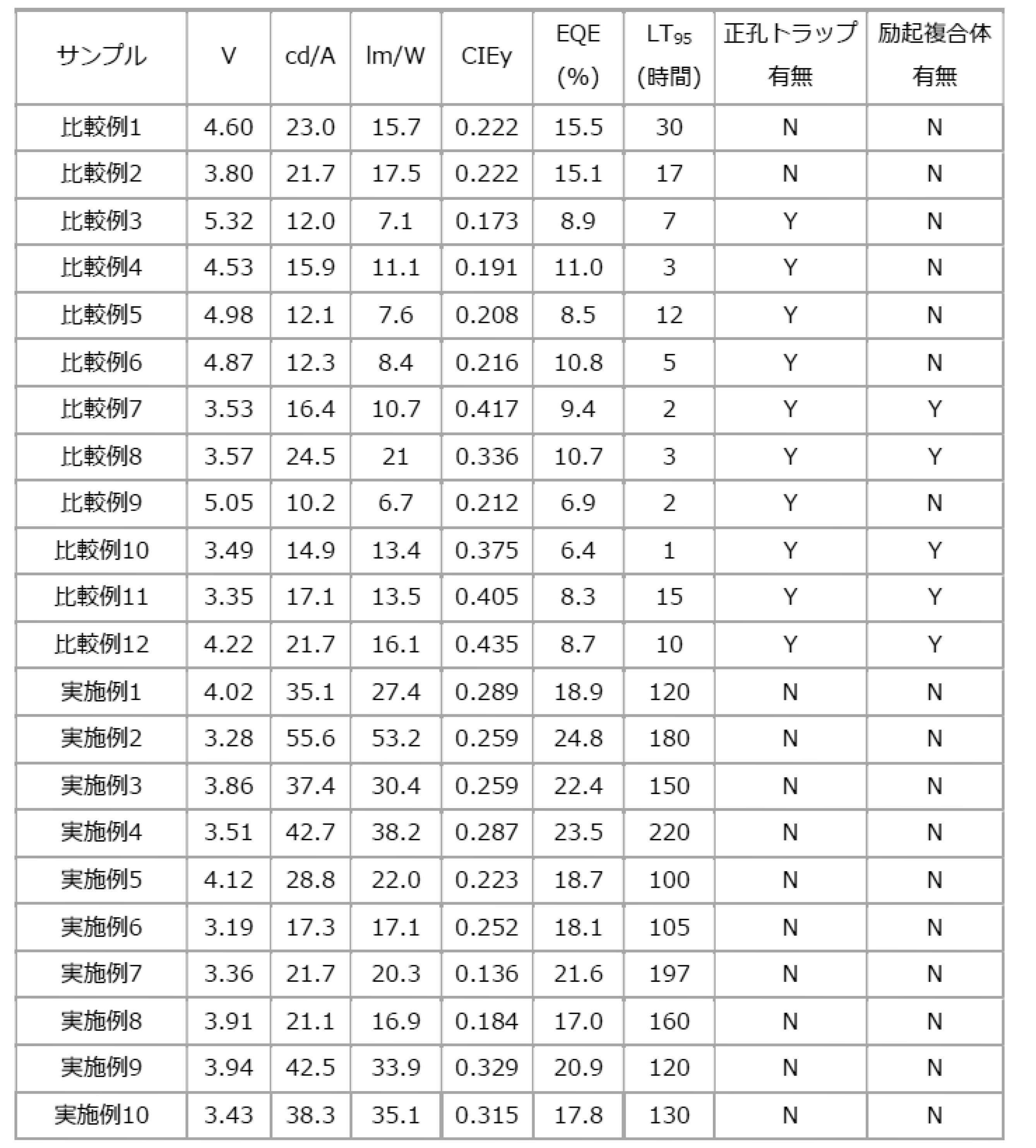
Light Emitting Characteristics of Organic Light Emitting Diodes
図20および図21に示すように、第1化合物および第2化合物のHOMOエネルギー準位のエネルギーバンドギャップが0.3eV以上となるように設計された比較例で製造された有機発光ダイオードでは、正孔トラップが発生した。それにより、駆動電圧が高くなり、電気的特性が非常に低下し、第1化合物から第2化合物へ遷移していない励起子のため、半値幅が増加した。特に、第1化合物および第2化合物のHOMOエネルギー準位のエネルギーバンドギャップが0.5eV以上と設計された比較例で製造された有機発光ダイオードでは、第1化合物のLUMOと第2化合物のHOMO間で励起複合体が形成され、電気的特性が低下し、半値幅が大幅に増加して色純度が低下したことを確認した。一方、第1化合物および第2化合物のHOMOエネルギー準位のバンドギャップが0.3eV未満と設計された実施例で製造された有機発光ダイオードでは、正孔トラップが発生せず、励起複合体も形成されなかった。 As shown in FIGS. 20 and 21, the organic light-emitting diode manufactured in the comparative example designed so that the energy bandgap of the HOMO energy levels of the first compound and the second compound is 0.3 eV or more is positive. A hole trap occurred. As a result, the driving voltage was increased, the electrical properties were significantly deteriorated, and the half-value width was increased due to the excitons not transitioning from the first compound to the second compound. In particular, in the organic light-emitting diode manufactured in the comparative example in which the energy bandgap of the HOMO energy levels of the first compound and the second compound was designed to be 0.5 eV or more, the LUMO of the first compound and the HOMO of the second compound It was confirmed that an excited complex was formed at , the electrical properties were deteriorated, the half-value width was greatly increased, and the color purity was decreased. On the other hand, in the organic light-emitting diode manufactured in the example in which the bandgap of the HOMO energy levels of the first compound and the second compound was designed to be less than 0.3 eV, no hole trap occurred and an excited complex was formed. it wasn't.
また、比較例3ないし比較例12で製造された有機発光ダイオードに比べ、実施例で製造された有機発光ダイオードの駆動電圧は、最大40.0%低下し、電流効率と電力効率、EQE、および発光寿命は、それぞれ最大445.1%、694.0%、287.5%、200倍向上した。 In addition, compared to the organic light emitting diodes manufactured in Comparative Examples 3 to 12, the driving voltage of the organic light emitting diodes manufactured in Examples was lowered by up to 40.0%, and the current efficiency, power efficiency, EQE, and The luminescence lifetime was improved up to 445.1%, 694.0%, 287.5% and 200 times, respectively.
さらに、第1化合物のΔESTより第2化合物のΔESTが大きく設計された比較例1および比較例2で製造された有機発光ダイオードに比べ、実施例で製造された有機発光ダイオードの駆動電圧は、最大30.7%低下し、電流効率と電力効率、EQE、および発光寿命は、それぞれ最大156.2%、238.9%、64.2%、11.9倍向上した。 Furthermore, compared to the organic light emitting diodes manufactured in Comparative Examples 1 and 2 in which the ΔEST of the second compound was designed to be larger than the ΔEST of the first compound, the driving voltage of the organic light emitting diodes manufactured in Examples was , decreased by up to 30.7%, and the current efficiency and power efficiency, EQE, and luminous lifetime improved by up to 156.2%, 238.9%, 64.2%, and 11.9 times, respectively.
以上、本発明の例示的な実施形態および実施例に基づき、本発明を説明したが、本発明は、前述した実施形態および実施例に記載された技術思想に限定されるものではない。むしろ、本発明の属する技術分野における通常の知識を有する者であれば、前述した実施形態および実施例に基づき、様々な変形や変更を容易に推考することができる。また、かかる変形や変更が全て本発明の権利範囲に属するということは、請求の範囲から明らかである。 Although the present invention has been described above based on the exemplary embodiments and examples of the present invention, the present invention is not limited to the technical ideas described in the above-described embodiments and examples. Rather, a person having ordinary knowledge in the technical field to which the present invention belongs can easily conceive of various modifications and changes based on the above-described embodiments and examples. Moreover, it is clear from the scope of claims that all such variations and modifications are within the scope of the present invention.
100、800、1000…有機発光表示装置、210、310、410、510、910、1110…第1電極、220、320、420、520、920、1120、1120A…発光層、230、330、430、530、930、1130…第2電極、240、340、440、640、740、940、1240、1340、1440、1540、1640、1740…発光物質層、D、D1、D2、D3、D4、D5、D6、D7…有機発光ダイオード、Tr…薄膜トランジスタ
100, 800, 1000... organic light emitting
Claims (21)
前記第1電極と対向する第2電極と、
前記第1電極と前記第2電極の間に位置し、少なくとも1つの発光物質層を含む発光層とを含み、
前記少なくとも1つの発光物質層は、第1化合物および第2化合物を含み、
前記第1化合物は、化学式(1):

で表される構造を有し、
前記第2化合物は、化学式(4):

で表される構造を有し、
前記第1化合物の最高被占軌道(HOMO)エネルギー準位(HOMO DF1 )と、前記第2化合物のHOMOエネルギー準位(HOMO DF2 )は、式(I):
│HOMO DF2 -HOMO DF1 │<0.3eV…(I)
を満たす、
有機発光ダイオード。 a first electrode;
a second electrode facing the first electrode;
a luminescent layer positioned between the first electrode and the second electrode and comprising at least one luminescent material layer;
the at least one luminescent material layer comprises a first compound and a second compound;
The first compound has the chemical formula (1) :
has a structure represented by
The second compound has the chemical formula (4):
has a structure represented by
The highest occupied molecular orbital (HOMO) energy level (HOMO DF1 ) of said first compound and the HOMO energy level (HOMO DF2 ) of said second compound are represented by formula (I):
│HOMO DF2 −HOMO DF1 │<0.3 eV (I)
satisfy the
Organic Light Emitting Diode.
前記第1電極と対向する第2電極と、
前記第1電極と前記第2電極の間に位置し、少なくとも1つの発光物質層を含む発光層とを含み、
前記少なくとも1つの発光物質層は、第1化合物および第2化合物を含み、
前記第1化合物は、化学式(1):

で表される構造を有し、
前記第2化合物は、化学式(4):

で表される構造を有し、
前記第1化合物の、最高被占軌道(HOMO)エネルギー準位と最低空軌道(LUMO)エネルギー準位との間のエネルギーバンドギャップは、2.6eV以上3.1eV以下である、
有機発光ダイオード。 a first electrode;
a second electrode facing the first electrode;
a luminescent layer positioned between the first electrode and the second electrode and comprising at least one luminescent material layer;
the at least one luminescent material layer comprises a first compound and a second compound;
The first compound has the chemical formula (1):
has a structure represented by
The second compound has the chemical formula (4):
has a structure represented by
The energy bandgap between the highest occupied molecular orbital (HOMO) energy level and the lowest unoccupied molecular orbital (LUMO) energy level of the first compound is 2 . 6 eV or more3 . is 1 eV or less ,
Organic Light Emitting Diode .
前記第1電極と対向する第2電極と、
前記第1電極と前記第2電極の間に位置し、少なくとも1つの発光物質層を含む発光層とを含み、
前記少なくとも1つの発光物質層は、第1化合物および第2化合物を含み、
前記第1化合物は、化学式(1):

で表される構造を有し、
前記第2化合物は、化学式(4):

で表される構造を有し、
前記第1化合物は、化学式(2A):

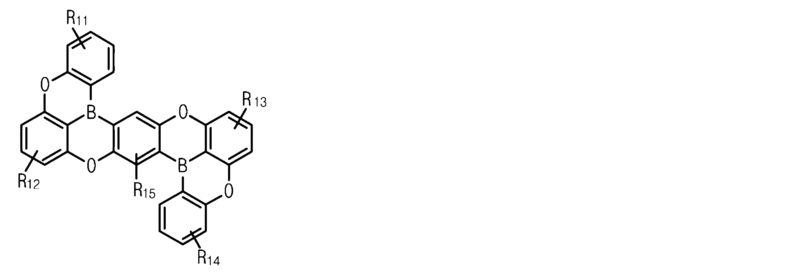
で表される構造を有する有機化合物を含む、
有機発光ダイオード。 a first electrode;
a second electrode facing the first electrode;
a luminescent layer positioned between the first electrode and the second electrode and comprising at least one luminescent material layer;
the at least one luminescent material layer comprises a first compound and a second compound;
The first compound has the chemical formula (1):
has a structure represented by
The second compound has the chemical formula (4):
has a structure represented by
The first compound has the chemical formula (2A) :
Including an organic compound having a structure represented by
Organic Light Emitting Diode.
前記第1電極と対向する第2電極と、
前記第1電極と前記第2電極の間に位置し、少なくとも1つの発光物質層を含む発光層とを含み、
前記少なくとも1つの発光物質層は、第1化合物および第2化合物を含み、
前記第1化合物は、化学式(1):
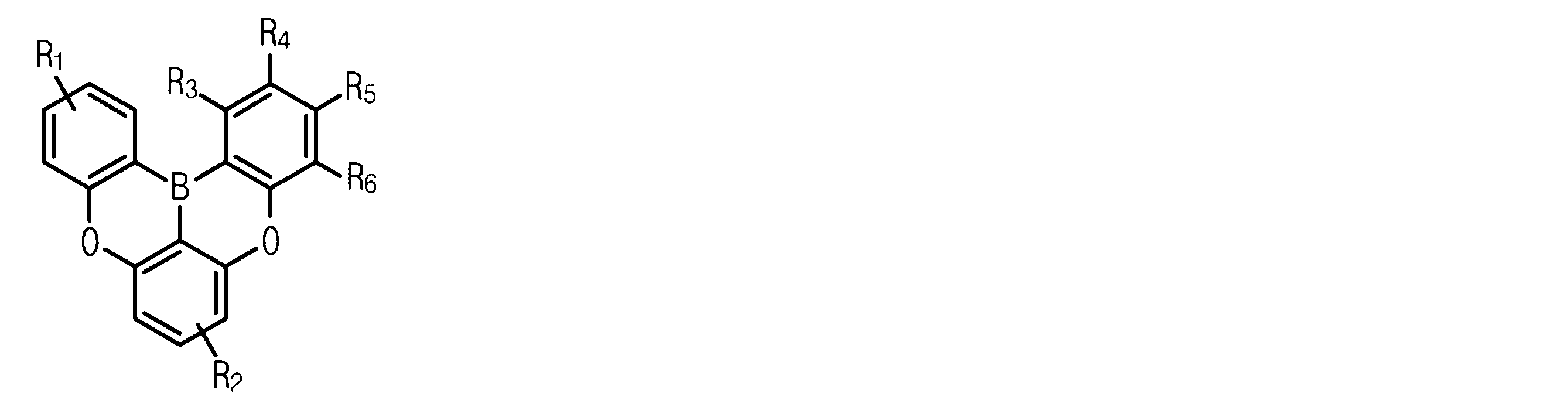
で表される構造を有し、
前記第2化合物は、化学式(4):
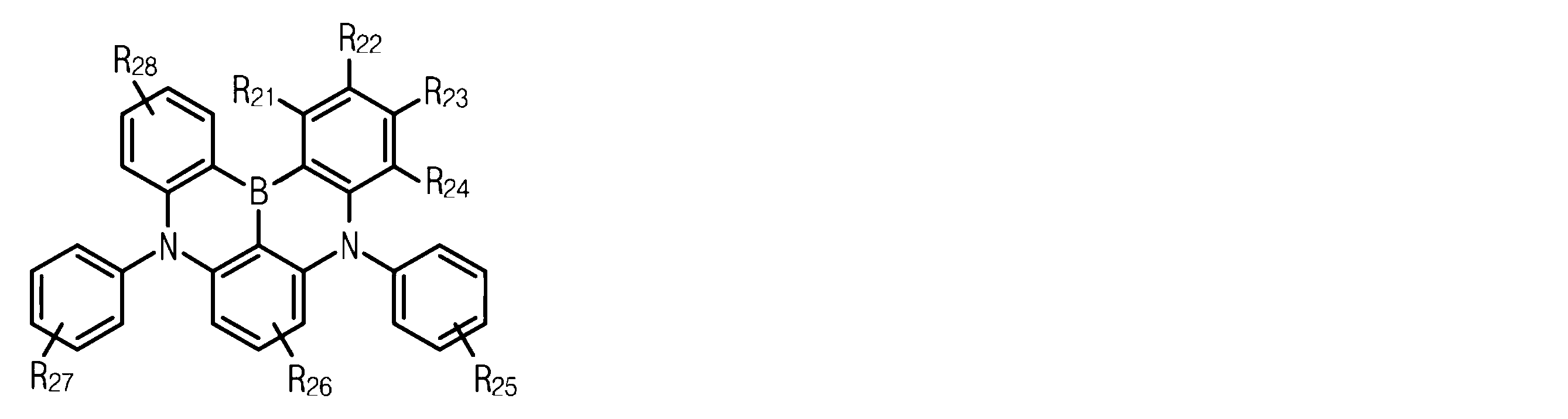
で表される構造を有し、
前記第1化合物は、化学式1-1から1-34:
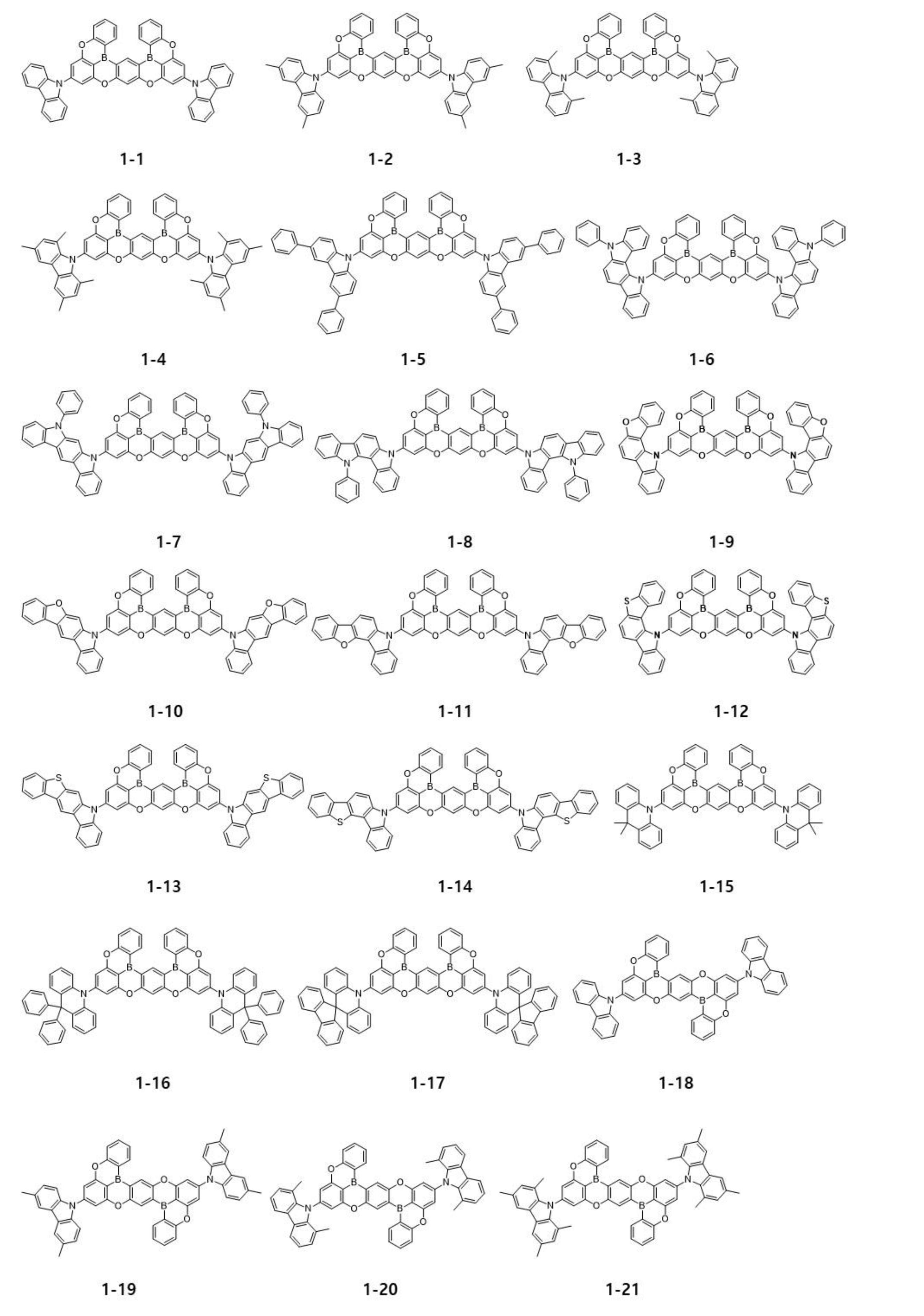

有機発光ダイオード。 a first electrode;
a second electrode facing the first electrode;
a luminescent layer positioned between the first electrode and the second electrode and comprising at least one luminescent material layer;
the at least one luminescent material layer comprises a first compound and a second compound;
The first compound has the chemical formula (1):
has a structure represented by
The second compound has the chemical formula (4):
has a structure represented by
The first compound has chemical formulas 1-1 to 1-34:
Organic Light Emitting Diode.
化学式(5A):
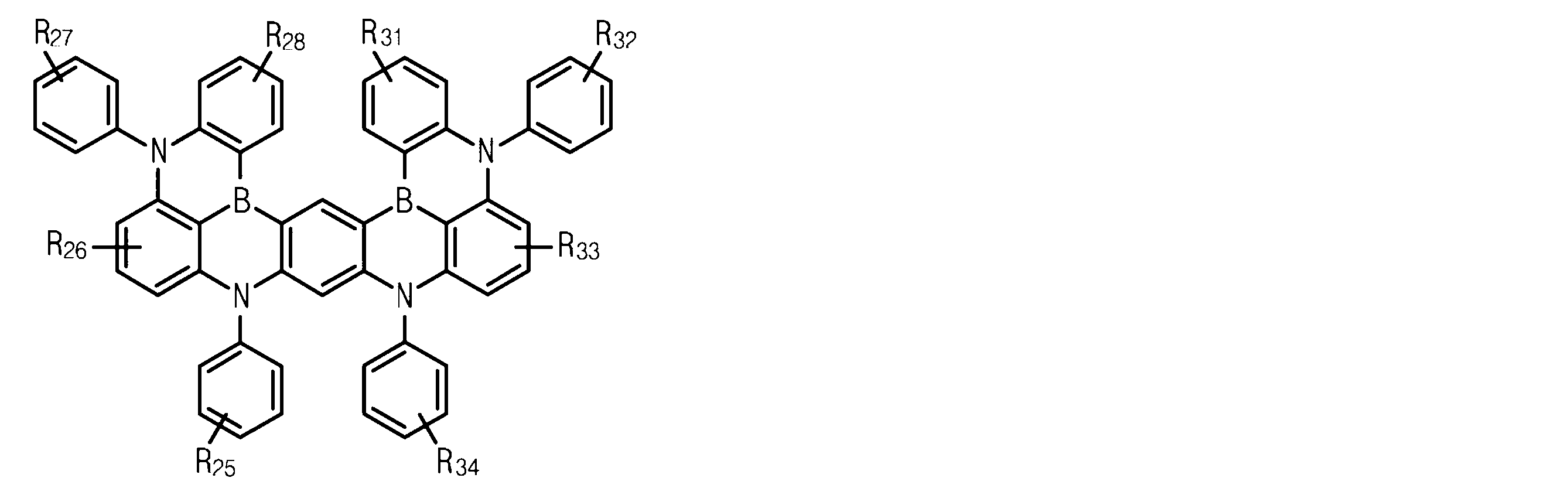
化学式(5B):

で表される構造を有する、
請求項1から5のいずれか1項に記載の有機発光ダイオード。 The second compound is
Chemical formula (5A) :
Chemical formula (5B):
having a structure represented by
6. An organic light-emitting diode according to any one of claims 1-5.
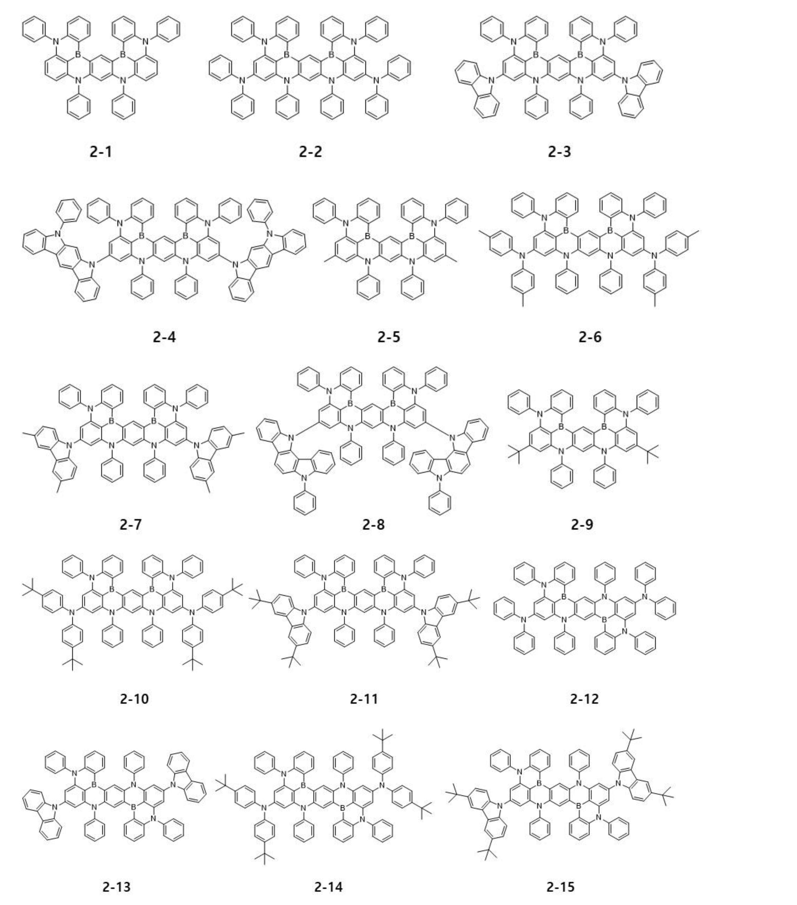
前記第1発光物質層は前記第1化合物を含み、前記第2発光物質層は前記第2化合物を含む、請求項1から4のいずれか1項に記載の有機発光ダイオード。 The at least one luminescent material layer includes a first luminescent material layer located between the first electrode and the second electrode and a luminescent material layer between the first electrode and the first luminescent material layer or the first luminescent material layer. a second luminescent material layer positioned between a layer and said second electrode;
5. The organic light emitting diode according to any one of claims 1 to 4 , wherein said first luminescent material layer comprises said first compound and said second luminescent material layer comprises said second compound.
前記第1発光部と前記第2発光部のうち、少なくとも一方は前記少なくとも1つの発光物質層を含む、請求項1から4のいずれか1項に記載の有機発光ダイオード。 The light-emitting layer includes a first light-emitting portion located between the first electrode and the second electrode, a second light-emitting portion located between the first light-emitting portion and the second electrode, and the first light-emitting portion. and a charge generation layer located between the second light emitting unit,
The organic light emitting diode according to any one of claims 1 to 4, wherein at least one of the first light emitting part and the second light emitting part comprises the at least one light emitting material layer.

で表される構造を有する、請求項1から4のいずれか1項に記載の有機発光ダイオード。 The first compound has the chemical formula (1′) :
5. An organic light emitting diode according to any one of claims 1 to 4, having a structure represented by

で表される構造を有する、請求項1から4のいずれか1項に記載の有機発光ダイオード。 The second compound has the chemical formula (4′) :
5. An organic light emitting diode according to any one of claims 1 to 4, having the structure represented by
前記基板上に位置する請求項1から請求項20のいずれか1項に記載の有機発光ダイオードとを含む有機発光装置。 a substrate;
21. An organic light emitting device comprising an organic light emitting diode according to any one of claims 1 to 20 located on said substrate.
Applications Claiming Priority (2)
| Application Number | Priority Date | Filing Date | Title |
|---|---|---|---|
| KR1020200149128A KR20220063369A (en) | 2020-11-10 | 2020-11-10 | Organic light emitting diode and organic light emitting device including the same |
| KR10-2020-0149128 | 2020-11-10 |
Publications (2)
| Publication Number | Publication Date |
|---|---|
| JP2022077011A JP2022077011A (en) | 2022-05-20 |
| JP7246453B2 true JP7246453B2 (en) | 2023-03-27 |
Family
ID=78414345
Family Applications (1)
| Application Number | Title | Priority Date | Filing Date |
|---|---|---|---|
| JP2021180958A Active JP7246453B2 (en) | 2020-11-10 | 2021-11-05 | Organic Light Emitting Diodes and Organic Light Emitting Devices |
Country Status (6)
| Country | Link |
|---|---|
| US (1) | US12201009B2 (en) |
| EP (1) | EP3995500A1 (en) |
| JP (1) | JP7246453B2 (en) |
| KR (1) | KR20220063369A (en) |
| CN (1) | CN114464747B (en) |
| TW (1) | TWI902958B (en) |
Families Citing this family (1)
| Publication number | Priority date | Publication date | Assignee | Title |
|---|---|---|---|---|
| JP2025135025A (en) * | 2022-06-23 | 2025-09-18 | 出光興産株式会社 | Organic electroluminescent elements, organic electroluminescent devices, electronic devices, light emitters, solar cells, and optical sensors |
Citations (16)
| Publication number | Priority date | Publication date | Assignee | Title |
|---|---|---|---|---|
| WO2015072537A1 (en) | 2013-11-18 | 2015-05-21 | 国立大学法人九州大学 | Light-emitting material, organic light-emitting element, and compound |
| WO2015102118A1 (en) | 2014-02-18 | 2015-07-09 | 学校法人関西学院 | Polycyclic aromatic compound |
| US20150236274A1 (en) | 2014-02-18 | 2015-08-20 | Kwansei Gakuin Educational Foundation | Polycyclic aromatic compound |
| CN107925006A (en) | 2015-07-24 | 2018-04-17 | 柯尼卡美能达株式会社 | Organic electroluminescent element, display device and lighting device |
| WO2018212169A1 (en) | 2017-05-16 | 2018-11-22 | 学校法人関西学院 | Polycyclic aromatic compound |
| WO2019035268A1 (en) | 2017-08-17 | 2019-02-21 | 学校法人関西学院 | Organic electroluminescent device |
| JP2020025099A (en) | 2018-08-07 | 2020-02-13 | エルジー ディスプレイ カンパニー リミテッド | Organic light-emitting diode and organic light-emitting device comprising the same |
| CN110790782A (en) | 2019-11-11 | 2020-02-14 | 北京大学深圳研究生院 | Dark blue organic luminescent material and preparation method and application thereof |
| US20200058874A1 (en) | 2018-08-17 | 2020-02-20 | Lg Display Co., Ltd. | Organic electroluminescence device |
| WO2020040298A1 (en) | 2018-08-23 | 2020-02-27 | 学校法人関西学院 | Organic electroluminescent element, display device, illumination device, luminescent layer forming composition, and compound |
| WO2020045681A1 (en) | 2018-08-31 | 2020-03-05 | 学校法人関西学院 | Organic electroluminescent element using light emitting material composed of polycyclic aromatic compound |
| WO2020101001A1 (en) | 2018-11-15 | 2020-05-22 | 学校法人関西学院 | Organic electroluminescence element, display device, and lighting device |
| JP2020136284A (en) | 2019-02-12 | 2020-08-31 | 学校法人関西学院 | Organic electroluminescent element |
| CN111647010A (en) | 2020-06-02 | 2020-09-11 | 苏州久显新材料有限公司 | Polycyclic boron-containing compound and electronic device thereof |
| US20210119168A1 (en) | 2019-10-01 | 2021-04-22 | Samsung Display Co., Ltd. | Organic electroluminescence device |
| US20220069235A1 (en) | 2020-09-02 | 2022-03-03 | Samsung Display Co., Ltd. | Light-emitting device and electronic apparatus including the same |
Family Cites Families (7)
| Publication number | Priority date | Publication date | Assignee | Title |
|---|---|---|---|---|
| EP1980627A1 (en) | 2007-04-13 | 2008-10-15 | Pangaea Biotech, S.A. | Method of determining a chemotherapeutic regime and survival expectancy for non small cell lung cancer based on EGFR/CSF-1/CA IX expression |
| CN110383521A (en) | 2017-02-16 | 2019-10-25 | 学校法人关西学院 | Organic electric-field light-emitting element |
| KR102622078B1 (en) | 2018-12-13 | 2024-01-05 | 엘지디스플레이 주식회사 | Organic light emitting diode and organic light emitting device haivng the diode |
| KR102647025B1 (en) | 2018-12-28 | 2024-03-12 | 엘지디스플레이 주식회사 | Organic compounds having improved luminsecent properties, organic light emitting diode and organic light emitting device including the compounds |
| KR102855864B1 (en) | 2019-11-28 | 2025-09-05 | 엘지디스플레이 주식회사 | Organic light emitting diode and organic light emitting device including the same |
| US11943998B2 (en) | 2019-11-28 | 2024-03-26 | Lg Display Co., Ltd. | Organic light emitting diode and organic light emitting device including the same |
| JP2021091644A (en) * | 2019-12-12 | 2021-06-17 | 学校法人関西学院 | Multimer compound |
-
2020
- 2020-11-10 KR KR1020200149128A patent/KR20220063369A/en active Pending
-
2021
- 2021-10-28 EP EP21205248.4A patent/EP3995500A1/en active Pending
- 2021-11-03 TW TW110140910A patent/TWI902958B/en active
- 2021-11-04 US US17/519,297 patent/US12201009B2/en active Active
- 2021-11-05 JP JP2021180958A patent/JP7246453B2/en active Active
- 2021-11-09 CN CN202111318695.4A patent/CN114464747B/en active Active
Patent Citations (20)
| Publication number | Priority date | Publication date | Assignee | Title |
|---|---|---|---|---|
| WO2015072537A1 (en) | 2013-11-18 | 2015-05-21 | 国立大学法人九州大学 | Light-emitting material, organic light-emitting element, and compound |
| WO2015102118A1 (en) | 2014-02-18 | 2015-07-09 | 学校法人関西学院 | Polycyclic aromatic compound |
| US20150236274A1 (en) | 2014-02-18 | 2015-08-20 | Kwansei Gakuin Educational Foundation | Polycyclic aromatic compound |
| CN106905367A (en) | 2014-02-18 | 2017-06-30 | 学校法人关西学院 | Polycyclc aromatic compound, polymer and its manufacture method and its application |
| US20190013478A1 (en) | 2015-07-24 | 2019-01-10 | Konica Minolta, Inc. | Organic electroluminescent element, display device, and illumination device |
| CN107925006A (en) | 2015-07-24 | 2018-04-17 | 柯尼卡美能达株式会社 | Organic electroluminescent element, display device and lighting device |
| US20200190115A1 (en) | 2017-05-16 | 2020-06-18 | Kwansei Gakuin Educational Foundation | Polycyclic aromatic compound |
| WO2018212169A1 (en) | 2017-05-16 | 2018-11-22 | 学校法人関西学院 | Polycyclic aromatic compound |
| CN110612304A (en) | 2017-05-16 | 2019-12-24 | 学校法人关西学院 | polycyclic aromatic compounds |
| WO2019035268A1 (en) | 2017-08-17 | 2019-02-21 | 学校法人関西学院 | Organic electroluminescent device |
| JP2020025099A (en) | 2018-08-07 | 2020-02-13 | エルジー ディスプレイ カンパニー リミテッド | Organic light-emitting diode and organic light-emitting device comprising the same |
| US20200058874A1 (en) | 2018-08-17 | 2020-02-20 | Lg Display Co., Ltd. | Organic electroluminescence device |
| WO2020040298A1 (en) | 2018-08-23 | 2020-02-27 | 学校法人関西学院 | Organic electroluminescent element, display device, illumination device, luminescent layer forming composition, and compound |
| WO2020045681A1 (en) | 2018-08-31 | 2020-03-05 | 学校法人関西学院 | Organic electroluminescent element using light emitting material composed of polycyclic aromatic compound |
| WO2020101001A1 (en) | 2018-11-15 | 2020-05-22 | 学校法人関西学院 | Organic electroluminescence element, display device, and lighting device |
| JP2020136284A (en) | 2019-02-12 | 2020-08-31 | 学校法人関西学院 | Organic electroluminescent element |
| US20210119168A1 (en) | 2019-10-01 | 2021-04-22 | Samsung Display Co., Ltd. | Organic electroluminescence device |
| CN110790782A (en) | 2019-11-11 | 2020-02-14 | 北京大学深圳研究生院 | Dark blue organic luminescent material and preparation method and application thereof |
| CN111647010A (en) | 2020-06-02 | 2020-09-11 | 苏州久显新材料有限公司 | Polycyclic boron-containing compound and electronic device thereof |
| US20220069235A1 (en) | 2020-09-02 | 2022-03-03 | Samsung Display Co., Ltd. | Light-emitting device and electronic apparatus including the same |
Also Published As
| Publication number | Publication date |
|---|---|
| JP2022077011A (en) | 2022-05-20 |
| EP3995500A1 (en) | 2022-05-11 |
| TW202219049A (en) | 2022-05-16 |
| US12201009B2 (en) | 2025-01-14 |
| TWI902958B (en) | 2025-11-01 |
| CN114464747B (en) | 2024-04-09 |
| CN114464747A (en) | 2022-05-10 |
| US20220149280A1 (en) | 2022-05-12 |
| KR20220063369A (en) | 2022-05-17 |
Similar Documents
| Publication | Publication Date | Title |
|---|---|---|
| US11800732B2 (en) | Organic light emitting diode and organic light emitting device having the same | |
| CN110818612A (en) | Organic compound, organic light emitting diode comprising the same, and organic light emitting device | |
| CN116419650A (en) | Organic light emitting diode and organic light emitting device including the organic light emitting diode | |
| KR102875305B1 (en) | Organic light emitting diode and organic light emitting device including the same | |
| US20230165132A1 (en) | Organic light emitting diode and organic light emitting device including thereof | |
| KR20210009698A (en) | Organic compounds having improved luminsecent properties, organic light emitting diode and organic light emitting device including the compounds | |
| JP7246453B2 (en) | Organic Light Emitting Diodes and Organic Light Emitting Devices | |
| JP7603149B2 (en) | Organic light-emitting diode and organic light-emitting device including the same | |
| KR102884407B1 (en) | Organic light emitting diode and organic light emitting device including the same | |
| CN118042855A (en) | Organic light emitting diode and organic light emitting device including the same | |
| KR20240103769A (en) | Organic light emitting diode | |
| JP7478266B2 (en) | Organic light-emitting diode and organic light-emitting device including the same | |
| KR102916237B1 (en) | Organic light emitting diode and organic light emitting device including the same | |
| KR20210046535A (en) | Organic compounds having improved luminsecent properties, organic light emitting diode and organic light emitting device including the compounds | |
| KR102861355B1 (en) | Organic light emitting diode and organic light emitting device including the same | |
| KR20220067131A (en) | Organic light emitting diode and organic light emitting device including the same | |
| KR20250093837A (en) | Organic light emitting diode and organic light emitting device having the diode | |
| KR20250094757A (en) | Organic compound, organic light emitting diode and organic light emitting device having the compound | |
| CN118251110A (en) | Organic light emitting diode and organic light emitting device including the same | |
| KR20210069560A (en) | Organic compounds having improved luminsecent properties, organic light emitting diode and organic light emitting device including the compounds | |
| KR20230088000A (en) | Organic light emitting display device |
Legal Events
| Date | Code | Title | Description |
|---|---|---|---|
| A621 | Written request for application examination |
Free format text: JAPANESE INTERMEDIATE CODE: A621 Effective date: 20211108 |
|
| A977 | Report on retrieval |
Free format text: JAPANESE INTERMEDIATE CODE: A971007 Effective date: 20220909 |
|
| A131 | Notification of reasons for refusal |
Free format text: JAPANESE INTERMEDIATE CODE: A131 Effective date: 20220920 |
|
| A521 | Request for written amendment filed |
Free format text: JAPANESE INTERMEDIATE CODE: A523 Effective date: 20221205 |
|
| TRDD | Decision of grant or rejection written | ||
| A01 | Written decision to grant a patent or to grant a registration (utility model) |
Free format text: JAPANESE INTERMEDIATE CODE: A01 Effective date: 20230221 |
|
| A61 | First payment of annual fees (during grant procedure) |
Free format text: JAPANESE INTERMEDIATE CODE: A61 Effective date: 20230314 |
|
| R150 | Certificate of patent or registration of utility model |
Ref document number: 7246453 Country of ref document: JP Free format text: JAPANESE INTERMEDIATE CODE: R150 |
|
| R250 | Receipt of annual fees |
Free format text: JAPANESE INTERMEDIATE CODE: R250 |