JP7244986B2 - Debris removal from high aspect structures - Google Patents
Debris removal from high aspect structures Download PDFInfo
- Publication number
- JP7244986B2 JP7244986B2 JP2017100802A JP2017100802A JP7244986B2 JP 7244986 B2 JP7244986 B2 JP 7244986B2 JP 2017100802 A JP2017100802 A JP 2017100802A JP 2017100802 A JP2017100802 A JP 2017100802A JP 7244986 B2 JP7244986 B2 JP 7244986B2
- Authority
- JP
- Japan
- Prior art keywords
- tip
- illumination
- collection
- chip
- present disclosure
- Prior art date
- Legal status (The legal status is an assumption and is not a legal conclusion. Google has not performed a legal analysis and makes no representation as to the accuracy of the status listed.)
- Active
Links
Images


Classifications
-
- G—PHYSICS
- G03—PHOTOGRAPHY; CINEMATOGRAPHY; ANALOGOUS TECHNIQUES USING WAVES OTHER THAN OPTICAL WAVES; ELECTROGRAPHY; HOLOGRAPHY
- G03F—PHOTOMECHANICAL PRODUCTION OF TEXTURED OR PATTERNED SURFACES, e.g. FOR PRINTING, FOR PROCESSING OF SEMICONDUCTOR DEVICES; MATERIALS THEREFOR; ORIGINALS THEREFOR; APPARATUS SPECIALLY ADAPTED THEREFOR
- G03F9/00—Registration or positioning of originals, masks, frames, photographic sheets or textured or patterned surfaces, e.g. automatically
- G03F9/70—Registration or positioning of originals, masks, frames, photographic sheets or textured or patterned surfaces, e.g. automatically for microlithography
- G03F9/7049—Technique, e.g. interferometric
- G03F9/7053—Non-optical, e.g. mechanical, capacitive, using an electron beam, acoustic or thermal waves
- G03F9/7061—Scanning probe microscopy, e.g. AFM, scanning tunneling microscopy
-
- G—PHYSICS
- G03—PHOTOGRAPHY; CINEMATOGRAPHY; ANALOGOUS TECHNIQUES USING WAVES OTHER THAN OPTICAL WAVES; ELECTROGRAPHY; HOLOGRAPHY
- G03F—PHOTOMECHANICAL PRODUCTION OF TEXTURED OR PATTERNED SURFACES, e.g. FOR PRINTING, FOR PROCESSING OF SEMICONDUCTOR DEVICES; MATERIALS THEREFOR; ORIGINALS THEREFOR; APPARATUS SPECIALLY ADAPTED THEREFOR
- G03F1/00—Originals for photomechanical production of textured or patterned surfaces, e.g., masks, photo-masks, reticles; Mask blanks or pellicles therefor; Containers specially adapted therefor; Preparation thereof
- G03F1/68—Preparation processes not covered by groups G03F1/20 - G03F1/50
- G03F1/72—Repair or correction of mask defects
-
- G—PHYSICS
- G01—MEASURING; TESTING
- G01N—INVESTIGATING OR ANALYSING MATERIALS BY DETERMINING THEIR CHEMICAL OR PHYSICAL PROPERTIES
- G01N15/00—Investigating characteristics of particles; Investigating permeability, pore-volume, or surface-area of porous materials
- G01N15/10—Investigating individual particles
- G01N15/14—Electro-optical investigation, e.g. flow cytometers
- G01N15/1456—Electro-optical investigation, e.g. flow cytometers without spatial resolution of the texture or inner structure of the particle, e.g. processing of pulse signals
-
- G—PHYSICS
- G03—PHOTOGRAPHY; CINEMATOGRAPHY; ANALOGOUS TECHNIQUES USING WAVES OTHER THAN OPTICAL WAVES; ELECTROGRAPHY; HOLOGRAPHY
- G03F—PHOTOMECHANICAL PRODUCTION OF TEXTURED OR PATTERNED SURFACES, e.g. FOR PRINTING, FOR PROCESSING OF SEMICONDUCTOR DEVICES; MATERIALS THEREFOR; ORIGINALS THEREFOR; APPARATUS SPECIALLY ADAPTED THEREFOR
- G03F7/00—Photomechanical, e.g. photolithographic, production of textured or patterned surfaces, e.g. printing surfaces; Materials therefor, e.g. comprising photoresists; Apparatus specially adapted therefor
- G03F7/70—Microphotolithographic exposure; Apparatus therefor
- G03F7/708—Construction of apparatus, e.g. environment aspects, hygiene aspects or materials
- G03F7/70908—Hygiene, e.g. preventing apparatus pollution, mitigating effect of pollution or removing pollutants from apparatus
- G03F7/70933—Purge, e.g. exchanging fluid or gas to remove pollutants
-
- G—PHYSICS
- G03—PHOTOGRAPHY; CINEMATOGRAPHY; ANALOGOUS TECHNIQUES USING WAVES OTHER THAN OPTICAL WAVES; ELECTROGRAPHY; HOLOGRAPHY
- G03F—PHOTOMECHANICAL PRODUCTION OF TEXTURED OR PATTERNED SURFACES, e.g. FOR PRINTING, FOR PROCESSING OF SEMICONDUCTOR DEVICES; MATERIALS THEREFOR; ORIGINALS THEREFOR; APPARATUS SPECIALLY ADAPTED THEREFOR
- G03F7/00—Photomechanical, e.g. photolithographic, production of textured or patterned surfaces, e.g. printing surfaces; Materials therefor, e.g. comprising photoresists; Apparatus specially adapted therefor
- G03F7/70—Microphotolithographic exposure; Apparatus therefor
- G03F7/708—Construction of apparatus, e.g. environment aspects, hygiene aspects or materials
- G03F7/70991—Connection with other apparatus, e.g. multiple exposure stations, particular arrangement of exposure apparatus and pre-exposure and/or post-exposure apparatus; Shared apparatus, e.g. having shared radiation source, shared mask or workpiece stage, shared base-plate; Utilities, e.g. cable, pipe or wireless arrangements for data, power, fluids or vacuum
-
- H—ELECTRICITY
- H01—ELECTRIC ELEMENTS
- H01L—SEMICONDUCTOR DEVICES NOT COVERED BY CLASS H10
- H01L21/00—Processes or apparatus adapted for the manufacture or treatment of semiconductor or solid state devices or of parts thereof
- H01L21/02—Manufacture or treatment of semiconductor devices or of parts thereof
- H01L21/027—Making masks on semiconductor bodies for further photolithographic processing not provided for in group H01L21/18 or H01L21/34
-
- G—PHYSICS
- G01—MEASURING; TESTING
- G01N—INVESTIGATING OR ANALYSING MATERIALS BY DETERMINING THEIR CHEMICAL OR PHYSICAL PROPERTIES
- G01N1/00—Sampling; Preparing specimens for investigation
- G01N1/02—Devices for withdrawing samples
- G01N1/04—Devices for withdrawing samples in the solid state, e.g. by cutting
-
- G—PHYSICS
- G01—MEASURING; TESTING
- G01Q—SCANNING-PROBE TECHNIQUES OR APPARATUS; APPLICATIONS OF SCANNING-PROBE TECHNIQUES, e.g. SCANNING PROBE MICROSCOPY [SPM]
- G01Q20/00—Monitoring the movement or position of the probe
- G01Q20/02—Monitoring the movement or position of the probe by optical means
-
- G—PHYSICS
- G01—MEASURING; TESTING
- G01Q—SCANNING-PROBE TECHNIQUES OR APPARATUS; APPLICATIONS OF SCANNING-PROBE TECHNIQUES, e.g. SCANNING PROBE MICROSCOPY [SPM]
- G01Q60/00—Particular types of SPM [Scanning Probe Microscopy] or microscopes; Essential components thereof
- G01Q60/24—AFM [Atomic Force Microscopy] or apparatus therefor, e.g. AFM probes
- G01Q60/38—Probes, their manufacture, or their related instrumentation, e.g. holders
- G01Q60/42—Functionalisation
-
- G—PHYSICS
- G01—MEASURING; TESTING
- G01Q—SCANNING-PROBE TECHNIQUES OR APPARATUS; APPLICATIONS OF SCANNING-PROBE TECHNIQUES, e.g. SCANNING PROBE MICROSCOPY [SPM]
- G01Q70/00—General aspects of SPM probes, their manufacture or their related instrumentation, insofar as they are not specially adapted to a single SPM technique covered by group G01Q60/00
- G01Q70/08—Probe characteristics
- G01Q70/10—Shape or taper
- G01Q70/12—Nanotube tips
-
- G—PHYSICS
- G01—MEASURING; TESTING
- G01Q—SCANNING-PROBE TECHNIQUES OR APPARATUS; APPLICATIONS OF SCANNING-PROBE TECHNIQUES, e.g. SCANNING PROBE MICROSCOPY [SPM]
- G01Q80/00—Applications, other than SPM, of scanning-probe techniques
Description
(関連出願に対する相互参照)
本特許出願は、2007年9月17日出願の米国特許出願第11/898,836号(米国特許第8,287,653号として交付された)の継続出願である、2012年10月15日出願の米国特許出願第13/652,114号(米国特許第8,696,818号として交付された)の分割出願である、2014年2月28日出願の米国特許出願第14/193,725号の一部継続出願である、2016年1月29日出願の同時係属中の米国特許出願第15/011,411号の一部継続出願であり、本特許出願の優先利益を主張する。これら全ては、援用により全体が本明細書に組み込まれる。
(Cross reference to related application)
This patent application is a continuation of U.S. patent application Ser. U.S. Patent Application Serial No. 14/193,725, filed February 28, 2014, which is a divisional application of filed U.S. Patent Application Serial No. 13/652,114 (issued as U.S. Patent No. 8,696,818) No. 15/011,411, filed Jan. 29, 2016, which is a continuation-in-part application of No. 1, and claims priority benefit of this patent application. all of which are incorporated herein by reference in their entirety.
(技術分野)
本開示は一般に、ナノ加工プロセスに関する。より詳細には、本開示は、ナノ加工プロセス中及び/又はナノ加工プロセス後のデブリ除去に関する。更に、本開示のデブリ除去処理は、基板に対する何らかの異物の除去に適用することができる。
(Technical field)
The present disclosure relates generally to nanofabrication processes. More particularly, the present disclosure relates to debris removal during and/or after nanofabrication processes. Further, the debris removal process of the present disclosure can be applied to remove any foreign matter from the substrate.
ナノ加工は、定義によれば、例えば、フォトリソグラフィ用マスク、半導体基板/ウェハ、又は走査型プローブ顕微鏡法(SPM)が実施可能な何らかの表面から物質のナノスケールの体積を機械的に除去することを伴う。本検討において、「基板」とは、ナノ加工が実施可能な何れかの対象物を指すことになる。 Nanofabrication is by definition the mechanical removal of nanoscale volumes of material from e.g. Accompanied by In this discussion, "substrate" will refer to any object amenable to nanofabrication.
フォトリソグラフィ用マスクの実施例には、標準的フォトマスク(193nm波長、液浸有り又は無し)、次世代リソグラフィ用マスク(インプリント、自己組織化など)、極紫外線リソグラフィ用マスク(EUV又はEUVL)、及び他の何れかの実行可能な又は有用なマスク技術が含まれる。基板と見なされる他の表面の実施例は、メンブレン、ペリクル膜、マイクロエレクトロ/ナノエレクトロメカニカルシステム・MEMS/NEMSである。本開示における用語「マスク」又は「基板」の使用は、上記の実施例を含むが、他のフォトマスク又は表面も適用可能とすることができることは、当業者には理解されよう。 Examples of photolithography masks include standard photomasks (193 nm wavelength, with or without immersion), next generation lithography masks (imprinting, self-assembly, etc.), extreme ultraviolet lithography masks (EUV or EUVL). , and any other feasible or useful mask technique. Examples of other surfaces that are considered substrates are membranes, pellicle membranes, microelectro/nanoelectromechanical systems/MEMS/NEMS. Those skilled in the art will appreciate that the use of the term "mask" or "substrate" in this disclosure includes the above examples, but may also be applicable to other photomasks or surfaces.
先行技術におけるナノ加工は、原子間力顕微鏡(AFM)のカンチレバーアーム上に位置決めされたチップ(例えば、ダイアモンド切削ビット)を用いて基板の表面に力を加えることにより実施することができる。より具体的に言うと、チップは、最初に基板表面に挿入することができ、次に表面に平行な平面(つまり、xy平面)で基板を引きずることができる。これにより、チップが基板に沿って引きずられるにつれて、基板からの物質の変位及び/又は除去が生じる。 Nanofabrication in the prior art can be performed by applying a force to the surface of the substrate with a tip (eg diamond cutting bit) positioned on the cantilever arm of an atomic force microscope (AFM). More specifically, the chip can first be inserted into the substrate surface and then dragged down the substrate in a plane parallel to the surface (ie the xy plane). This results in displacement and/or removal of material from the substrate as the tip is dragged along the substrate.
このナノ加工の結果として、デブリ(基板表面に対する何らかの異物を含む)が基板上に生成される。より具体的には、物質が基板から除去されると、ナノ加工プロセス中に小粒子が生じる場合がある。これらの粒子は、場合によっては、ナノ加工プロセスが完了すると基板上に残存する。このような粒子は、例えば、基板上に存在するトレンチ及び/又はキャビティにおいて見られることが多い。 As a result of this nano-fabrication, debris (including any foreign matter to the substrate surface) is generated on the substrate. More specifically, small particles may be generated during the nanofabrication process when material is removed from the substrate. These particles sometimes remain on the substrate once the nanofabrication process is completed. Such particles are often found, for example, in trenches and/or cavities present on the substrate.
デブリ、粒子又は基板に対する異物を除去するために、特に高アスペクトのフォトリソグラフィ用マスク及び電子回路においては、湿式洗浄技術が使われてきた。より具体的には、液体状態での化学物質の使用及び/又はマスク又は回路全体の撹拌を用いることができる。しかしながら、化学的方法及び撹拌方法(例えば、メガソニック(高周波超音波)撹拌など)は、高アスペクト比の構造及びマスク光近接効果補正特徴部(すなわち、一般に極めて小さい特徴部であるので、これらの特徴部は、結像するのではなく、むしろパターンを形成するためにマスク設計者により有利に利用される回折パターンを形成する)の両方に悪影響を及ぼし、又は破壊する場合がある。 Wet cleaning techniques have been used to remove debris, particles, or contaminants from the substrate, especially in high aspect photolithographic masks and electronics. More specifically, the use of chemicals in the liquid state and/or agitation of the entire mask or circuit can be used. However, chemical and agitation methods (e.g., megasonic (high-frequency ultrasonic) agitation, etc.) are not suitable for high aspect ratio structures and mask optical proximity correction features (i.e., typically very small features). Features may adversely affect or destroy both the imaging, but rather forming a diffraction pattern that is advantageously used by the mask designer to form the pattern.
高アスペクト形状及び構造が化学物質及び撹拌により特に破壊されやすい理由をより良く理解するために、このような形状及び構造は、定義によれば多大な表面積を含み、そのため熱力学的に極めて不安定であることを想起する必要がある。従って、これらの形状及び構造は、化学的及び/又は機械的エネルギーが加えられると層間剥離及び/又は他の形態の破壊に極めて脆弱である。 To better understand why high aspect shapes and structures are particularly susceptible to destruction by chemicals and agitation, such shapes and structures by definition contain a large surface area and are therefore thermodynamically very unstable. It should be remembered that As such, these shapes and structures are extremely vulnerable to delamination and/or other forms of failure when chemical and/or mechanical energy is applied.
インプリントリソグラフィ及びEUV(又はEUVL)において、複写されるリソグラフィ表面から粒子を離しておくためのペリクルの使用は、現在では適していない点に留意することは重要である。ペリクルを使用できない技術は一般に、ウェハへのパターン転写能力を阻害する粒子汚染による不良の影響をより受けやすい。ペリクルは、EUVマスク向けに開発されているが、DUVペリクルマスクに関するこれまでの経験が示すように、ペリクルの使用は、限界粒子及び他の汚染物が表面上に落下するのを軽減するだけであり(完全には防げない)、その後の高エネルギー光子へ何れかの曝露は、これらの粒子を大きな付着力でマスク表面に固定する傾向となる。更に、これらの技術は、より小さなフィーチャサイズ(1~300nm)で実施することができ、通常使用することができる標準的な湿式洗浄の実施の際に損傷をより受けやすくする。EUV又はEUVLの特定ケースにおいて、この技術は、使用中、及び場合によっては使用待ちの保管中に基板を真空環境にすることが必要となる可能性がある。標準的な湿式洗浄技術を使用するためには、この真空を破壊しなければならず、これにより更なる粒子汚染につながりやすい。 It is important to note that in imprint lithography and EUV (or EUVL) the use of pellicles to keep particles away from the lithographic surface to be copied is not currently suitable. Technologies that cannot use pellicles are generally more susceptible to failure due to particle contamination that inhibits the ability to transfer patterns to the wafer. Pellicles have been developed for EUV masks, but experience with DUV pellicle masks indicates that the use of pellicles only reduces the amount of stray particles and other contaminants that fall on the surface. Yes (but not completely preventable), any subsequent exposure to high-energy photons tends to anchor these particles to the mask surface with great adhesion. Furthermore, these techniques can be performed at smaller feature sizes (1-300 nm), making them more susceptible to damage during standard wet cleaning practices that are commonly used. In the specific case of EUV or EUVL, this technique may require the substrate to be in a vacuum environment during use and possibly storage awaiting use. To use standard wet cleaning techniques, this vacuum must be broken, which tends to lead to further particle contamination.
基板からデブリを除去するための現在利用可能な別の方法において、極低温洗浄システム及び技術を用いる。例えば、高アスペクト形状及び/又は構造を含む基板は、砂の代わりに二酸化炭素粒子を用いて効果的に「サンドブラスト」することができる。 Another currently available method for removing debris from substrates uses cryogenic cleaning systems and techniques. For example, substrates containing high aspect features and/or structures can be effectively "sandblasted" using carbon dioxide particles instead of sand.
しかしながら、先行技術における極低温洗浄システム及びプロセスでも同様に、高アスペクト特徴部に悪影響を及ぼす又はこれを破壊することが知られている。更に、極低温洗浄プロセスは、基板の比較的大きな領域に影響を及ぼす(例えば、ナノメートル台の寸法を有するデブリを洗浄するために、処理される領域は、幅がおよそ10ミリメートル又はそれを超える場合がある)。結果として、そこからデブリを除去する必要のない基板領域が、それでも極低温洗浄プロセス、並びにこれに関連する潜在的構造破壊性エネルギーに曝される。ナノレジームとマイクロレジームとの間には多くの物理的相違点が存在することに留意すべきであり、本明細書において、ナノ粒子洗浄プロセスに関連する相違点に焦点を当てることになる。ナノとマクロスケールの洗浄プロセスの間には多くの類似点があるが、多くの決定的な相違点もまた存在する。本開示において、ナノスケールの共通した定義が有用であり、これは1~100nmのサイズ範囲を定義する。本明細書で評価されるプロセスの多くがこの範囲未満で(原子スケールまで)生じることができ、また、この範囲より大きな粒子(マイクロレジームまで)に影響を及ぼすことができるので、このサイズ範囲は、汎用の範囲である。 However, cryogenic cleaning systems and processes in the prior art are also known to adversely affect or destroy high aspect features. Furthermore, the cryogenic cleaning process affects relatively large areas of the substrate (e.g., to clean debris having dimensions on the order of nanometers, the treated area may be on the order of 10 millimeters or more in width). sometimes). As a result, areas of the substrate from which debris does not need to be removed are still exposed to the cryogenic cleaning process and the potentially structurally destructive energy associated therewith. It should be noted that there are many physical differences between the nanoregime and the microregime, and the focus here will be on the differences related to the nanoparticle cleaning process. While there are many similarities between nano- and macro-scale cleaning processes, there are also many critical differences. A common definition of nanoscale is useful in this disclosure, which defines the size range from 1 to 100 nm. This size range is because many of the processes evaluated herein can occur below this range (up to the atomic scale) and can affect particles larger than this range (up to the micro-regime). , in the general-purpose range.
マクロとナノの粒子洗浄プロセス間の幾つかの物理的な相違点には、表面積、平均自由行程、熱的及び電界効果を含む輸送関連特性が含まれる。このリストの最初の2つは、粒子の熱機械的化学的挙動により関連性があるが、最後の1つは、粒子の電磁場との相互作用とより関係している。熱輸送現象は、粒子周りの熱機械的物理化学現象であり、赤外波長レジームにおける粒子と電磁場との相互作用であるという点で、これらの2つのレジームを分ける。これらの相違点の幾つかを機能的に明らかにするために、高アスペクトのラインアンドスペース構造(深さ70nm、幅40nm~AR=1.75)の底部にトラップされたナノ粒子の思考実験の例を仮定する。マクロスケールプロセスでこの粒子を洗浄除去するために、粒子を取り除くのに必要とされるエネルギーは、基板上の特徴部又はパターンに損傷を与えるのに必要とされるエネルギーとほぼ同じであり、これにより、この高アスペクトのラインアンドスペース構造を損傷無しで洗浄することは不可能である。マクロスケールの洗浄プロセス(水、界面活性剤、音波撹拌など)においては、ナノ粒子が除去されるエネルギーレベルにおいて、周囲の特徴部又はパターンもまた損傷を受ける。ナノ粒子に対してナノ距離内で正確にナノ的に鋭利な(又はナノスケール)構造を扱う技術的能力がもしあれば、ナノ粒子を洗浄除去するためのエネルギーをナノ粒子だけに印加することができる。ナノスケールの洗浄プロセスにおいて、ナノ粒子を除去するために必要とされるエネルギーは、ナノ粒子にだけ印加され、基板上にある周囲の特徴部又はパターンには印加されない。 Some physical differences between macro- and nano-particle cleaning processes include transport-related properties including surface area, mean free path, thermal and field effects. The first two in this list are more relevant to the thermomechanical chemical behavior of the particles, while the last one is more to do with the particles' interaction with the electromagnetic field. The heat transport phenomenon separates these two regimes in that it is a thermomechanical physico-chemical phenomenon around particles and the interaction of particles with electromagnetic fields in the infrared wavelength regime. To functionally clarify some of these differences, a thought experiment of nanoparticles trapped at the bottom of a high-aspect line-and-space structure (70 nm deep, 40 nm wide ~ AR = 1.75) was performed. Assume an example. To wash away this particle in a macroscale process, the energy required to remove the particle is about the same as the energy required to damage features or patterns on the substrate, which Therefore, it is impossible to clean this high aspect line and space structure without damage. In macroscale cleaning processes (water, surfactants, sonic agitation, etc.), at the energy levels at which nanoparticles are removed, surrounding features or patterns are also damaged. Given the technical ability to handle nano-sharp (or nano-scale) structures precisely within nano-distances for nanoparticles, it is possible to apply energy only to the nanoparticles to wash them away. can. In nanoscale cleaning processes, the energy required to remove nanoparticles is applied only to the nanoparticles and not to the surrounding features or patterns on the substrate.
最初に、粒子の表面領域特性を見ると、理論上の粒子(ここでは完全球体としてモデル化される)がナノスケールレジームに近づくにつれて明瞭になる数学的スケーリングの相違点が存在する。物質のバルク特性は、物質の体積で評価されるが、表面は、外部面積により評価される。仮定的粒子においては、その体積は、その粒子の直径に対して3乗で反比例して減少するが、表面積は、粒子の直径に対して2乗で減少する。この差は、マクロ及びマイクロスケールの直径での粒子の挙動を支配する物質特性が、ナノレジームでは無視できるように(より小さく)なることを意味する。これらの特性の実施例には、粒子の質量及び慣性特性が含まれ、音波撹拌又はレーザ衝撃などの一部の洗浄技術にとって重大な考慮事項である。 First, looking at the surface area properties of the particles, there are differences in mathematical scaling that become apparent as theoretical particles (here modeled as perfect spheres) approach the nanoscale regime. Bulk properties of a material are measured by the volume of the material, while surfaces are measured by the external area. For a hypothetical particle, the volume decreases inversely as the cube of the particle's diameter, while the surface area decreases as the square of the particle's diameter. This difference means that the material properties that govern particle behavior at macro- and microscale diameters become negligible (smaller) in the nano-regime. Examples of these properties include particle mass and inertial properties, which are critical considerations for some cleaning techniques such as sonic agitation or laser bombardment.
ここで考察する次の輸送特性は平均自由行程である。マクロからマイクロレジームにおいて、流体(液体と気体の両方、及び混合状態)は、その挙動において連続体流れとして正確にモデル化することができる。AFMチップ及びナノ粒子など、ナノスケール又はそれよりも小さい間隙で離隔された表面を考えると、これらの流体を連続体と見なすことはできない。これは、流体が古典的流れモデルに従って移動するのではなく、より正確には希薄気体又は真空の弾道的原子運動に関連付けることができることを意味する。標準温度及び圧力での気体中の平均原子又は分子(直径がおよそ0.3nm)において、計算平均自由行程(つまり、分子が平均して別の原子又は分子に衝突する前に一直線に進む距離)は、およそ94nmであり、これはAFM走査プローブの大きな距離である。流体は気体よりも遥かに密度が高いので、遥かに小さな平均自由行程を有することになるが、あらゆる流体に対する平均自由行程は、原子又は分子の直径より小さくなることはできない点に留意しなければならない。典型的なチップに対して上記で与えられた0,3nmという仮定原子又は分子の直径と、1nm程度に小さいとすることができる非接触走査モード時の表面平均分離距離とを比較すると、最も密度の高い流体を除けば、AFMチップ先端と走査される表面との間の流体環境は、希薄気体から近真空までの流体特性の範囲で挙動することになる。上記の評価における知見は、マクロからナノスケールにスケール変更される際に熱流体プロセスが基本的に異なるように挙動することを示すのに不可欠である。これは、化学反応、環境に遊離した粒子などの生成物の除去、帯電又は電荷中和、及び熱又は熱エネルギーの輸送など、様々なプロセス態様の機構及び動力学に影響を及ぼす。 The next transport property considered here is the mean free path. In the macro-to-micro regime, fluids (both liquids and gases, and mixed states) can be accurately modeled in their behavior as continuum flows. Considering surfaces separated by gaps on the nanoscale or smaller, such as AFM tips and nanoparticles, these fluids cannot be considered a continuum. This means that fluids do not move according to classical flow models, but can be more precisely related to the ballistic atomic motion of dilute gases or vacuums. Calculated mean free path (i.e., the distance a molecule travels in a straight line before colliding with another atom or molecule on average) for an average atom or molecule (approximately 0.3 nm in diameter) in a gas at standard temperature and pressure is approximately 94 nm, which is a large distance for AFM scanning probes. Since fluids are much denser than gases, they will have much smaller mean free paths, but it should be noted that the mean free path for any fluid cannot be smaller than the diameter of an atom or molecule. not. Comparing the assumed atomic or molecular diameter of 0.3 nm given above for a typical tip with the surface average separation distance during the non-contact scanning mode, which can be as small as 1 nm, the highest density Except for high λ fluids, the fluid environment between the AFM tip tip and the surface being scanned will behave in a range of fluid properties from dilute gases to near vacuum. The findings in the above evaluation are essential to show that thermofluid processes behave fundamentally differently when scaled from the macro to the nanoscale. This affects the mechanisms and kinetics of various process aspects such as chemical reactions, removal of products such as particles released into the environment, charging or charge neutralization, and heat or thermal energy transport.
マクロ及びナノからサブナノスケールへの既知の熱輸送の相違点は、走査型熱プローブ顕微鏡を用いた研究により見出された。1つの初期に見出された相違点は、熱エネルギーの輸送速度がナノスケールの距離にわたってマクロスケールよりも1桁小さい場合があることである。このようにして、走査型熱プローブ顕微鏡は、チップから表面までの離隔距離がナノ又はオングストロームスケール程に小さい非接触モードで走査している表面に対して、場合によっては数百度の温度差まで加熱されたナノプローブを用いて機能することができる。この低い熱輸送の理由は、流体における平均自由行程に関する前節にて暗示されている。しかしながら、熱輸送の一形態である黒体輻射が強化されている。ナノスケールの距離で、所与の温度での黒体スペクトル放射輝度に関するプランク限界を超える場合があることが実験的に示された。従って、熱輸送の大きさが減少するだけでなく、主要な輸送タイプが、伝導/対流から希薄真空流体挙動と一致する黒体へと変化する。 Known differences in heat transport from macro- and nano-to sub-nanoscales were discovered by studies using scanning thermal probe microscopy. One early-discovered difference is that the transport rate of thermal energy can be an order of magnitude smaller over nanoscale distances than at the macroscale. In this manner, scanning thermal probe microscopy can heat up to temperature differentials of potentially hundreds of degrees for surfaces that are scanned in a non-contact mode with tip-to-surface separations as small as the nano- or Angstrom scale. can work with nanoprobes that have been engineered. The reason for this low heat transfer is alluded to in the previous section on mean free paths in fluids. However, blackbody radiation, a form of heat transport, is enhanced. It has been experimentally shown that at nanoscale distances the Planck limit for blackbody spectral radiance at a given temperature may be exceeded. Thus, not only is the magnitude of heat transport reduced, but the dominant transport type changes from conduction/convection to blackbody consistent with dilute vacuum fluid behavior.
場(他の実施可能な例と比較してその長い波長に起因して、電磁場が本明細書での主要な目的とする実施例である)の相互作用における相違点は、本検討において、波長関連及び他の量子効果(特にトンネリング)として更に分類することができる。ナノスケールにおいて、発生源(ここにおいて、主要な発生源としてか、又は比較的遠距離場発生源の変更形態としてかを問わず、AFMチップの先端として想定される)と表面との間の電磁場の挙動は、遠距離場発生源が経験することになる分解能に対する波長依存の回折限界に従わないことになる。この挙動は、一般に近接場光学と呼ばれ、近接場走査型光学顕微鏡(NSOM)などの走査型プローブ技術では大きな成功を収めて使用されている。計測工学での応用を超えて、近接場の挙動は、互いにナノ距離で離間した全てのナノスケールサイズの物体の電磁相互作用に影響を及ぼす可能性がある。言及した次の近接場挙動は、量子トンネリングであり、ここでは粒子、特に電子は、古典的には通り抜けることのできない障壁を超えて運ぶことができる。この現象は、マクロスケールでは見られない手段によるエネルギー輸送を可能にし、走査型トンネリング顕微鏡(STM)及び一部の固体電子デバイスで利用されている。最後に、近接励起及びプラズモン共鳴の検出など、ナノスケールにおいて電磁場に関して(限定されないが)見られることの多いより難解な量子効果が存在するが、現在の検討がマクロとナノスケールの物理過程間の根本的な相違点の十分な論証を与えることが、当業者には理解されるであろう。 Differences in the interaction of fields (electromagnetic fields being the primary example of interest here, due to their longer wavelengths compared to other possible examples) are, in this discussion, the wavelength They can be further classified as related and other quantum effects (particularly tunneling). At the nanoscale, the electromagnetic field between the source (here envisioned as the tip of the AFM tip, whether as the primary source or as a modification of the relatively far-field source) and the surface behavior will not follow the wavelength-dependent diffraction limit to the resolution that the far-field source will experience. This behavior is commonly referred to as near-field optics and has been used with great success in scanning probe techniques such as near-field scanning optical microscopy (NSOM). Beyond metrology applications, near-field behavior can influence the electromagnetic interaction of all nanoscale-sized objects separated from each other by nanodistances. The next near-field behavior mentioned is quantum tunneling, where particles, especially electrons, can be transported across barriers that are classically impenetrable. This phenomenon enables energy transport by means not seen at the macroscale and is exploited in scanning tunneling microscopes (STM) and some solid state electronic devices. Finally, there are more esoteric quantum effects that are often seen (but not limited to) with electromagnetic fields at the nanoscale, such as near-field excitation and detection of plasmon resonance, but the current investigation is focused on the relationship between macro- and nanoscale physical processes. It will be appreciated by those skilled in the art that a sufficient demonstration of the underlying differences will be provided.
以下において、用語「表面エネルギー」は、仕事(ここにおいて、基板及びチップそれぞれの表面へのデブリの付着という仕事)を実行するのに利用可能な表面の熱力学特性を指すのに使用することができる。古典的にこれを計算する1つの方法は、
G(p,T)=U+pV-TS
として与えられるギブズ自由エネルギーであり、
ここで、
U=内部エネルギー
p=圧力
V=体積
T=温度、及び
S=エントロピーである。
In the following, the term "surface energy" may be used to refer to the thermodynamic properties of a surface available to perform work, here the work of adhering debris to the surface of the substrate and chip, respectively. can. One way to classically calculate this is
G(p,T)=U+pV-TS
is the Gibbs free energy given by
here,
U = internal energy, p = pressure, V = volume, T = temperature, and S = entropy.
現行の実施において、圧力、体積、及び温度を変えないので(これらのパラメータを同様に操作して所望の効果を得ることも可能なので、必然ではないが)、詳細には検討しない。従って、上記の式中で操作される項は、内部エネルギーと以下で検討する方法における駆動機構としてのエントロピーだけとなる。プローブチップ表面は洗浄される基板よりも清浄である(つまり、デブリ及び意図しない表面汚染がない)ことが意図されているので、当然ながら、エントロピーが基板上方のチップ表面を優先的に汚染する熱力学的駆動機構である(次いで、その後、軟質物質のクリーナパレットを汚染する)。内部エネルギーは、パレット、チップ、デブリ、及び基板表面の間で、そのそれぞれの表面エネルギーにより特徴付けられる熱力学特性によって操作される。微分表面エネルギーをギブズ自由エネルギーと関連付ける1つの方法は、単軸性張力P下で半径r及び長さlの円柱に対する高温(つまり、その融点温度の有意な部分)での工学材料のクリープ特性に関する理論的発展を考察することである:
dG=-P*dl+γ*dA
ここで、
γ=表面エネルギー密度[J/m2]、及び
A=表面積[m2]
In current practice, pressure, volume, and temperature are not varied (although not necessary, as these parameters can be similarly manipulated to achieve desired effects) and will not be discussed in detail. Therefore, the only terms manipulated in the above equation are internal energy and entropy as the driving mechanism in the methods discussed below. Since the probe tip surface is intended to be cleaner (i.e., free of debris and unintentional surface contamination) than the substrate being cleaned, it should be understood that thermal entropy preferentially contaminates the tip surface above the substrate. A mechanical drive (which then subsequently contaminates the soft material cleaner pallets). Internal energy is manipulated between pallet, chip, debris, and substrate surfaces by thermodynamic properties characterized by their respective surface energies. One way to relate the differential surface energy to the Gibbs free energy relates to the creep properties of engineered materials at high temperatures (i.e., a significant fraction of their melting temperature) for a cylinder of radius r and length l under uniaxial tension P It is to consider the theoretical development:
dG=-P*dl+γ*dA
here,
γ = surface energy density [J/m2], and A = surface area [m2]
物体の応力及び外因性表面エネルギーがそのギブズ自由エネルギーにおける因子であるという知見は、これらの因子(表面エネルギー密度γに加えて)を操作して、チップ及びその後に続く軟質パレットにデブリを可逆的に優先して付着させるステップを実行することができると確信させるものである。これを行う手段には、応力印加(外的か内的かを問わず)及び温度が含まれる。この駆動プロセスは常に、優先的に基板の汚染物質を除去してその後に軟質パレットを優先的に汚染する微分表面エネルギー勾配を提供するために、正味のΔGが<0となる一連の表面相互作用をもたらすことになる点に留意されたい。これは、ボールが斜面をより低いエネルギー状態に優先的に転がり落ちることに類似していると考えることができる(但し、ここにおいて、熱力学的表面エネルギーの勾配には、系全体での総体的な無秩序又はエントロピーも含まれる)。図6は、本明細書に記載する方法が選択的に汚染を除去して選択的に軟質パッチ上に堆積させる熱力学的ギブズ自由エネルギーの下り勾配を提供することができる、表面相互作用の1つの実施可能なセットを示す。このシーケンスは、低表面エネルギーのフッ化炭素系材料をダイアモンドなどの低表面エネルギーチップ材料と共に用いる現行の実施態様に対する役割を担うと考えられる理論的機構の1つである。 The finding that an object's stress and extrinsic surface energy are factors in its Gibbs free energy suggests that these factors (in addition to the surface energy density γ) can be manipulated to reversibly move debris to the tip and subsequent soft pallets. It convinces that the step of preferentially attaching to the can be performed. Means for doing this include stress application (whether external or internal) and temperature. This driving process always follows a series of surface interactions with a net ΔG<0 to provide a differential surface energy gradient that preferentially removes substrate contaminants followed by soft pallets. Note that it will result in This can be thought of as analogous to a ball rolling down a slope preferentially to a lower energy state (where the thermodynamic surface energy gradient does not include the global (including random disorder or entropy). FIG. 6 illustrates one of the surface interactions that the methods described herein can provide for the thermodynamic Gibbs free energy downslope that selectively decontaminates and selectively deposits on soft patches. shows one possible set. This sequence is one of the theoretical mechanisms believed to play a role for current implementations of using low surface energy fluorocarbon-based materials with low surface energy tip materials such as diamond.
少なくとも上記のことを鑑みると、デブリ、汚染物質、粒子又は基板表面に対する何らかの異物を除去するための新規の装置及び方法に対する要望があり、詳細には、高アスペクト比構造を有する基板、フォトマスク光近接効果補正特徴部などをこのようなナノスケールの構造及び/又は特徴部を破壊することなく洗浄することができる新規の装置及び方法に対する要望がある。 In view of at least the above, there is a need for new apparatus and methods for removing debris, contaminants, particles, or any foreign material to substrate surfaces, particularly substrates having high aspect ratio structures, photomask optical There is a need for new apparatus and methods that can clean proximity effect correction features and the like without destroying such nanoscale structures and/or features.
本開示の一態様によれば、汚染物質を検出するためのナノスケール計測システムが提供される。本システムは、走査プローブ顕微鏡(SPM)チップ、照射源、照射検出器、アクチュエータ、及びコントローラを含む。照射源は、入射する照射をSPMチップ上に配向するように構成され配置される。照射検出器は、SPMチップから試料照射を受けるように構成され配置され、該試料照射は、入射する照射によって引き起こされる。アクチュエータシステムは、ナノスケール計測システムに動作可能に連結され、SPMチップと照射源及び照射検出器のうちの少なくとも1つとの間に相対移動を生じるように構成される。コントローラは、アクチュエータシステム及び照射検出器に動作可能に連結され、コントローラは、試料照射に対する照射検出器の第1の応答に基づいて第1の信号を受信するように構成されており、第1の信号に基づいて、アクチュエータシステムによってSPMチップと照射検出器及び照射源のうちの少なくとも1つとの間に相対移動を生じるように構成される。 According to one aspect of the present disclosure, a nanoscale metrology system for detecting contaminants is provided. The system includes a scanning probe microscope (SPM) tip, illumination source, illumination detector, actuator, and controller. The illumination source is constructed and arranged to direct incident illumination onto the SPM chip. The illumination detector is constructed and arranged to receive sample illumination from the SPM chip, the sample illumination caused by incident illumination. An actuator system is operatively coupled to the nanoscale metrology system and configured to produce relative movement between the SPM tip and at least one of the illumination source and the illumination detector. A controller is operably coupled to the actuator system and the illumination detector, the controller configured to receive a first signal based on a first response of the illumination detector to the illumination of the sample; Based on the signal, an actuator system is configured to cause relative movement between the SPM tip and at least one of the radiation detector and the radiation source.
本開示のナノスケール計測システムの一態様によれば、アクチュエータシステムは、SPMチップに動作可能に連結され、アクチュエータシステムは、SPMチップを第1の軸の周りで回転させるように構成された回転アクチュエータを含む。 According to one aspect of the nanoscale metrology system of the present disclosure, an actuator system is operably coupled to the SPM tip, the actuator system being a rotary actuator configured to rotate the SPM tip about a first axis. including.
本開示におけるナノスケール計測システムの一態様によれば、照射源は、X線源、レーザ、可視光源、赤外光源、紫外光源、又は電子ビーム源である。 According to one aspect of the nanoscale metrology system of the present disclosure, the illumination source is an X-ray source, a laser, a visible light source, an infrared light source, an ultraviolet light source, or an electron beam source.
本開示におけるナノスケール計測システムの一態様によれば、コントローラは更に、第1の信号に基づいて試料照射の第1の周波数領域スペクトルを生成し、第1の周波数領域スペクトルからバックグラウンド周波数領域スペクトルを差し引くことによって第2の周波数領域スペクトルを生成し、第2の周波数領域スペクトルに基づいてアクチュエータシステムによってSPMチップと照射検出器及び照射源のうちの少なくとも1つとの間に相対移動を生じるように構成される。本開示におけるナノスケール計測システムの一態様によれば、コントローラは更に、SPMチップが実質的に汚染物質を含まない場合に、SPMチップの照射に対する照射検出器の応答に基づいてバックグラウンド周波数領域スペクトルを生成するように構成される。 According to one aspect of the nanoscale metrology system of the present disclosure, the controller further generates a first frequency-domain spectrum of sample illumination based on the first signal; to produce a second frequency domain spectrum by subtracting the second frequency domain spectrum and to cause relative movement between the SPM tip and at least one of the radiation detector and the radiation source by the actuator system based on the second frequency domain spectrum Configured. According to one aspect of the nanoscale metrology system of the present disclosure, the controller further comprises a background frequency domain spectrum based on the response of the illumination detector to illumination of the SPM chip when the SPM chip is substantially free of contaminants. is configured to generate
本開示におけるナノスケール計測システムの一態様によれば、コントローラは更に、試料照射に対する照射検出器の第2の応答に基づいて第2の信号を受信し、第1の信号と第2の信号との間の差違に基づいてアクチュエータシステムによってSPMチップと照射検出器及び照射源のうちの少なくとも1つとの間に相対移動を生じるように構成される。本開示におけるナノスケール計測システムの一態様によれば、コントローラは更に、第1の信号と第2の信号との間の差違に基づいてSPMチップと照射検出器及び照射源のうちの少なくとも1つとの間に所定の大きさの相対移動を生じるように構成される。 According to one aspect of the nanoscale metrology system of the present disclosure, the controller further receives a second signal based on a second response of the illumination detector to the illumination of the sample, the first signal and the second signal relative movement between the SPM tip and at least one of the radiation detector and the radiation source by an actuator system based on a difference between the . According to one aspect of the nanoscale metrology system of the present disclosure, the controller further comprises controlling the SPM chip and at least one of the illumination detector and illumination source based on the difference between the first signal and the second signal. is configured to produce a relative movement of a predetermined magnitude between
本開示の一態様によれば、回収器を備えたナノスケール計測システムが提供される。本計測システムは、回収器、照射源、照射検出器、走査プローブ顕微鏡(SPM)チップ、及びアクチュエータシステムを含む。本回収器は、回収器の第1の表面上にある第1の内縁部と、回収器の第2の表面上に第1の表面の反対側にある第2の内縁部と、第1の内縁部から第2の内縁部まで延びて、回収ポケット又は回収スルーホールの少なくとも一部を定める内部表面と、を有することができる。照射源は、回収器の内部表面から試料照射を受けるように構成されて配置され、試料照射は入射する照射によって引き起こされる。アクチュエータシステムは、SPMチップに動作可能に連結され、SPMチップを回収器に対して移動させて、少なくとも1つの粒子又はデブリをSPMチップから回収器に移送するように構成される。 According to one aspect of the present disclosure, a nanoscale metrology system with a collector is provided. The metrology system includes a collector, illumination source, illumination detector, scanning probe microscope (SPM) tip, and actuator system. The collector has a first inner edge on the first surface of the collector, a second inner edge on the second surface of the collector opposite the first surface, and a first an inner surface extending from the inner edge to a second inner edge and defining at least a portion of the collection pocket or collection through-hole. The illumination source is constructed and arranged to receive sample illumination from an interior surface of the collector, the sample illumination being caused by the incident illumination. An actuator system is operably coupled to the SPM chip and configured to move the SPM chip relative to the collector to transfer at least one particle or debris from the SPM chip to the collector.
本開示における計測システムの一態様によれば、回収スルーホールの幅は、第1の表面から第2の表面に向かって回収器を通過する方向に沿って増加する。 According to one aspect of the metrology system of the present disclosure, the width of the collection through-hole increases along the direction through the collector from the first surface to the second surface.
本開示における計測システムの一態様によれば、第1の内縁部は、回収ポケット又は回収スルーホールの矩形の輪郭を定める。本開示の一態様によれば、矩形輪郭の各線分の長さは10mm以下である。 According to one aspect of the metrology system of the present disclosure, the first inner edge defines a rectangular outline of the collection pocket or collection through-hole. According to one aspect of the present disclosure, each line segment of the rectangular contour has a length of 10 mm or less.
本開示における計測システムの一態様によれば、第1の内縁部は、回収ポケット又は回収スルーホールの三角形の輪郭を定める。本開示の一態様によれば、三角形輪郭の各線分の長さは10mm以下である。 According to one aspect of the metrology system of the present disclosure, the first inner edge defines a triangular profile of the collection pocket or collection through-hole. According to one aspect of the present disclosure, each line segment of the triangular outline has a length of 10 mm or less.
本開示における計測システムの一態様によれば、第1の内縁部は回収ポケット又は回収スルーホールの弓形断面を定め、該弓形断面は、円形、楕円形又は卵形の輪郭である。本開示の一態様によれば、第1の内縁部は円形輪郭を定め、円形輪郭の直径は10mm以下である。 According to one aspect of the metrology system of the present disclosure, the first inner edge defines an arcuate cross-section of the collection pocket or collection through-hole, the arcuate cross-section being of circular, elliptical or oval profile. According to one aspect of the disclosure, the first inner edge defines a circular profile, and the circular profile has a diameter of 10 mm or less.
本開示における計測システムの一態様によれば、計測システムは更に、アクチュエータシステムに動作可能に連結されたコントローラを含み、コントローラは、SPMチップを第1の内縁部に対して引きずることによってSPMチップから回収ポケット又は回収スルーホールに粒子を移送するように構成される。 According to one aspect of the metrology system of the present disclosure, the metrology system further includes a controller operably coupled to the actuator system, the controller pulling the SPM tip away from the SPM tip by dragging it against the first inner edge. Configured to transfer particles to a collection pocket or collection through-hole.
本開示における計測システムの一態様によれば、回収器の内部表面は、スルーホール通路を形成する。本開示の一態様によれば、スルーホール通路は、切頂四面体通路、円錐台形通路、切頂四面体通路、又は角錐台形通路である。 According to one aspect of the metrology system of the present disclosure, the interior surface of the collector forms a through-hole passageway. According to one aspect of the present disclosure, the through-hole passageway is a truncated tetrahedral passageway, a frustoconical passageway, a truncated tetrahedral passageway, or a truncated pyramidal passageway.
本開示における計測システムの一態様によれば、SPMチップは、四面体形状、円錐形状、又は角錐形状を含む。 According to one aspect of the metrology system of the present disclosure, the SPM tip includes a tetrahedral, conical, or pyramidal shape.
本開示における計測システムの一態様によれば、回収ポケット又は回収スルーホールは、計測システムに取り外し可能に装着される。 According to one aspect of the metrology system of the present disclosure, a retrieval pocket or retrieval through-hole is removably attached to the metrology system.
本開示の一態様によれば、粒子回収及び計測システムが提供される。本粒子回収及び計測システムは、走査型プローブ顕微鏡(SPM)チップと、基板を支持するよう構成されたステージと、作動システムと、照射源と、照射検出器と、コントローラと、を含む。作動システムは、ステージ及びSPMチップに動作可能に連結され、該作動システムは、SPMチップをステージに対して移動させるように構成されている。照射源は、計測位置と光学的に連通しており、また、照射検出器は、計測位置と光学的に連通している。コントローラは、作動システム、照射源、及び照射検出器に動作可能に連結される。コントローラは更に、基板に近接した位置から計測位置にSPMチップを移動させ、計測位置からの第1の試料照射に対する照射検出器の応答を示す第1の信号を照射検出器から受信する、ように構成されており、第1の試料照射は、照射源からの第1の入射する照射によって引き起こされる。 According to one aspect of the present disclosure, a particle collection and metering system is provided. The particle collection and metrology system includes a scanning probe microscope (SPM) tip, a stage configured to support a substrate, an actuation system, an illumination source, an illumination detector, and a controller. An actuation system is operably coupled to the stage and the SPM tip, the actuation system configured to move the SPM tip relative to the stage. The illumination source is in optical communication with the measurement location and the illumination detector is in optical communication with the measurement location. A controller is operably linked to the actuation system, the illumination source, and the illumination detector. The controller further moves the SPM tip from a position proximate to the substrate to the measurement position and receives a first signal from the illumination detector indicative of the response of the illumination detector to the first sample illumination from the measurement position. Configured, a first sample illumination is caused by a first incident illumination from the illumination source.
本開示における粒子回収及び計測システムの一態様によれば、計測位置は、SPMチップの少なくとも一部分上に配置され、コントローラは更に、第1の入射する照射を計測位置に照射することによって、第1の試料照射を引き起こすように構成される。 According to one aspect of the particle collection and metrology system of the present disclosure, the measurement location is disposed on at least a portion of the SPM chip, and the controller further directs a first incident radiation to the measurement location, thereby causing the first of sample irradiation.
本開示における粒子回収及び計測システムの一態様によれば、粒子回収及び計測システムは更に粒子回収器を含み、計測位置は、粒子回収器の少なくとも一部分上に配置される。コントローラは更に、第1の入射する照射を計測位置に照射することによって第1の試料照射を引き起こすように構成される。 According to one aspect of the particle collection and measurement system of the present disclosure, the particle collection and measurement system further includes a particle collector, and the measurement location is disposed on at least a portion of the particle collector. The controller is further configured to cause the first sample irradiation by directing the first incident irradiation onto the measurement location.
本開示における粒子回収及び計測システムの一態様によれば、コントローラは更に、SPMチップを介して基板から計測位置に粒子を移送するように構成される。 According to one aspect of the particle collection and metrology system of the present disclosure, the controller is further configured to transfer particles from the substrate to the measurement location via the SPM chip.
本開示における粒子回収及び計測システムの一態様によれば、粒子回収及び計測システムは更に、材料のパッチを含み、該材料は、基板の表面エネルギーよりも低い表面エネルギーを有し、SPMチップは、表面上に材料のナノスケールコーティングを含む。 According to one aspect of the particle collection and metrology system of the present disclosure, the particle collection and metrology system further includes a patch of material, the material having a surface energy lower than the surface energy of the substrate, the SPM chip comprising: It contains a nanoscale coating of material on the surface.
本開示における粒子回収及び計測システムの一態様によれば、コントローラは更に、SPMチップとパッチとの間に接触を生じさせ、これによってSPMチップを材料でコーティングするように構成される。 According to one aspect of the particle collection and metrology system of the present disclosure, the controller is further configured to cause contact between the SPM tip and the patch, thereby coating the SPM tip with material.
本開示における粒子回収及び計測システムの一態様によれば、作動システムは、SPMチップに動作可能に連結されたチップ作動システムと、ステージに動作可能に連結されたステージ作動システムと、を含む。チップ作動システムは、SPMチップを基部に対して移動させるように構成され、ステージ作動システムは、ステージを基部に対して移動させるように構成される。 According to one aspect of the particle collection and metrology system of the present disclosure, the actuation system includes a tip actuation system operably coupled to the SPM tip and a stage actuation system operably coupled to the stage. A tip actuation system is configured to move the SPM tip relative to the base, and a stage actuation system is configured to move the stage relative to the base.
本開示における粒子回収及び計測システムの一態様によれば、粒子回収器は、回収ポケット又は回収スルーホールである。粒子回収器は、少なくとも第1の内縁部を含む。少なくとも第1の内縁部は、三角形、矩形、円形、楕円形、又は卵形の輪郭のうちの1つを定める。本開示の一態様によれば、第1の内縁部は、三角形又は矩形の輪郭を定め、三角形又は矩形の輪郭の各線分は10mm以下の長さを含む。本開示の一態様によれば、第1の内縁部は円形輪郭を定め、円形輪郭の直径は10mm以下である。 According to one aspect of the particle collection and metering system of the present disclosure, the particle collector is a collection pocket or collection through-hole. The particle collector includes at least a first inner edge. At least the first inner edge defines one of a triangular, rectangular, circular, elliptical, or oval contour. According to one aspect of the disclosure, the first inner edge defines a triangular or rectangular profile, and each line segment of the triangular or rectangular profile includes a length of 10 mm or less. According to one aspect of the disclosure, the first inner edge defines a circular profile, and the circular profile has a diameter of 10 mm or less.
本開示における粒子回収及び計測システムの一態様によれば、粒子回収器は、回収器の第1の表面上にある第1の内縁部と、回収器の第2の表面上に第1の表面の反対側にある第2の内縁部と、第1の内縁部から第2の内縁部まで延びる内部表面とを含む。本開示の一態様によれば、内部表面はスルーホール通路を形成する。スルーホール通路は、切頂四面体通路、円錐台形通路、又は角錐台形通路である。 According to one aspect of the particle collection and metrology system of the present disclosure, the particle collector has a first inner edge on a first surface of the collector and a first surface on a second surface of the collector. and an inner surface extending from the first inner edge to the second inner edge. According to one aspect of the present disclosure, the inner surface forms a through-hole passageway. The through-hole passages are truncated tetrahedral passages, frusto-conical passages, or frusto-pyramidal passages.
本開示における粒子回収及び計測システムの一態様によれば、SPMチップは、四面体形状、円錐形状、又は角錐形状を含む。 According to one aspect of the particle collection and metrology system of the present disclosure, the SPM tip includes a tetrahedral, conical, or pyramidal shape.
本開示における粒子回収及び計測システムの一態様によれば、パッチは、計測システムに取り外し可能に装着される。本開示における粒子回収及び計測システムの一態様によれば、回収ポケット又は回収スルーホールは、ステージに取り外し可能に装着される。 According to one aspect of the particle collection and measurement system of the present disclosure, the patch is removably attached to the measurement system. According to one aspect of the particle collection and metrology system of the present disclosure, collection pockets or collection through-holes are removably attached to the stage.
本開示の一態様によれば、走査プローブ顕微鏡(SPM)チップを使用して粒子の組成を特定する方法が提供される。本方法は、粒子をSPMチップに移送するステップと、照射源からの第1の入射する照射をSPMチップに照射するステップと、第1の入射する照射によって引き起こされた第1の試料照射を照射検出器により検出するステップと、第1の試料照射に応答した照射検出器からの第1の信号に基づいて、SPMチップと照射源及び照射検出器のうちの少なくとも1つとの間に相対移動を生じさせるステップと、を含む。 According to one aspect of the present disclosure, a method of determining particle composition using a scanning probe microscope (SPM) tip is provided. The method includes the steps of transferring particles to the SPM tip, illuminating the SPM tip with a first incident radiation from an illumination source, and illuminating a first sample radiation caused by the first incident radiation. detecting by the detector; and relative movement between the SPM tip and at least one of the illumination source and the illumination detector based on a first signal from the illumination detector in response to the first sample illumination. and .
SPMチップ上の粒子の組成を特定する方法の一態様によれば、本方法は、第1の信号に基づいて試料照射の第1の周波数領域スペクトルを生成するステップと、第1の周波数領域スペクトルからバックグラウンド周波数領域スペクトルを差し引くことによって第2の周波数領域スペクトルを生成するステップと、第2の周波数領域スペクトルに基づいてSPMチップと照射源及び照射検出器のうちの少なくとも1つとの間に相対移動を生じさせるステップと、を更に含む。 According to one aspect of a method of determining composition of particles on an SPM chip, the method comprises the steps of: generating a first frequency domain spectrum of sample illumination based on a first signal; generating a second frequency-domain spectrum by subtracting the background frequency-domain spectrum from the second frequency-domain spectrum; causing movement.
SPMチップ上の粒子の組成を特定する方法の一態様によれば、本方法は、SPMチップが実質的に汚染物質を含まない場合に、SPMチップの照射に対する照射検出器の応答に基づいてバックグラウンド周波数領域スペクトルを生成するステップを更に含む。 According to one aspect of the method of determining the composition of particles on an SPM chip, the method comprises backing based on the response of the illumination detector to illumination of the SPM chip when the SPM chip is substantially free of contaminants. Further comprising generating a ground frequency domain spectrum.
SPMチップ上の粒子の組成を特定する方法の一態様によれば、本方法は更に、照射源からの第2の入射する照射をSPMチップに照射するステップと、第2の入射する照射によって引き起こされた第2の試料照射を照射検出器により検出するステップと、第2試料照射に応答した照射検出器からの第2の信号に基づいて、SPMチップと照射源及び照射検出器のうちの少なくとも1つとの間に相対移動を生じさせるステップと、を含む。 According to one aspect of the method of determining the composition of particles on an SPM chip, the method further comprises irradiating the SPM chip with a second incident radiation from the radiation source; detecting the second sample illumination with the illumination detector; and at least one of the SPM chip and the illumination source and the illumination detector based on a second signal from the illumination detector in response to the second sample illumination. causing relative movement between one and the other.
SPMチップ上の粒子の組成を特定する方法の一態様によれば、本方法は、第2の信号と第1の信号との間の差違に基づいて、SPMチップと照射源及び照射検出器のうちの少なくとも1つとの間に相対移動を生じさせるステップを更に含む。 According to one aspect of the method of determining the composition of particles on the SPM chip, the method comprises determining the composition of the SPM chip and the radiation source and radiation detector based on the difference between the second signal and the first signal. further comprising the step of causing relative movement between at least one of the
SPMチップ上の粒子の組成を特定する方法の一態様によれば、照射源からの第1の入射する照射は、X線、可視光、赤外光、紫外光、電子ビーム、及びレーザのうちの少なくとも1つである。SPMチップ上の粒子の組成を特定する方法の一態様によれば、照射源からの第2の入射する照射は、X線、可視光、赤外光、紫外光、電子ビーム、及びレーザのうちの少なくとも1つである。第2の入射する照射は、第1の入射する照射とは異なるタイプの照射である。一態様において、第1の試料照射は、第1の入射する照射がSPMチップと相互作用することによって生成される。一態様において、相互作用は、第1の入射する照射のSPMチップによる反射、屈折、又は吸収及び再放出のうちの1又は2以上を含むことができる。一態様において、第1の試料照射は、第1の入射する照射がSPMチップ上に配置されたデブリと相互作用することによって生成される。一態様において、相互作用は、第1の入射する照射のSPMチップ上に配置されたデブリによる反射、屈折、又は吸収及び再放出のうちの1又は2以上を含むことができる。 According to one aspect of the method of determining the composition of particles on an SPM chip, the first incident radiation from the radiation source is selected from among X-rays, visible light, infrared light, ultraviolet light, electron beam, and laser. is at least one of According to one aspect of the method of determining the composition of particles on an SPM chip, the second incident radiation from the radiation source is selected from X-rays, visible light, infrared light, ultraviolet light, electron beam, and laser. is at least one of The second incident radiation is a different type of radiation than the first incident radiation. In one aspect, the first sample illumination is generated by interaction of the first incident illumination with the SPM tip. In one aspect, the interaction can include one or more of reflection, refraction, or absorption and re-emission by the SPM tip of the first incident radiation. In one aspect, the first sample illumination is generated by interaction of the first incident illumination with debris disposed on the SPM chip. In one aspect, the interaction can include one or more of reflection, refraction, or absorption and re-emission by debris disposed on the SPM chip of the first incident radiation.
SPMチップ上の粒子の組成を特定する方法の一態様によれば、本方法は更に、照射源からの第1の入射する照射の強度又は周波数を調整するステップを含む。一態様において、本方法は更に、照射源からの第2の入射する照射の強度又は周波数を調整するステップを含む。 According to one aspect of the method of determining the composition of particles on an SPM chip, the method further comprises adjusting the intensity or frequency of the first incident radiation from the radiation source. In one aspect, the method further includes adjusting the intensity or frequency of the second incident illumination from the illumination source.
本開示の一態様によれば、基板から除去された粒子の組成を特定するための方法が提供される。本方法は、基板から走査プローブ顕微鏡(SPM)チップに粒子を移送するステップと、照射源からの第1の入射する照射を粒子に照射するステップと、照射検出器にて粒子から第1の入射する照射によって引き起こされる第1の試料照射を受けるステップと、を含む。 According to one aspect of the present disclosure, a method is provided for determining the composition of particles removed from a substrate. The method comprises the steps of transferring particles from a substrate to a scanning probe microscope (SPM) tip; irradiating the particles with a first incident radiation from an illumination source; receiving a first irradiation of the sample caused by a second irradiation.
基板から除去された粒子の組成を特定する本方法の態様によれば、粒子からの第1の試料照射は、粒子がSPMチップ上に配置されている間に照射検出器によって受け取られる。 According to aspects of the method for determining the composition of particles removed from a substrate, a first sample illumination from the particles is received by an illumination detector while the particles are positioned on the SPM chip.
基板から除去された粒子の組成を決定する本方法の一態様によれば、基板からSPMチップへの粒子の移送は、SPMチップを基板に接触させて、基板に対してSPMチップを移動させるステップを含む。 According to one aspect of the method of determining the composition of particles removed from a substrate, transferring the particles from the substrate to the SPM tip includes the steps of contacting the SPM tip with the substrate and moving the SPM tip relative to the substrate. including.
基板から除去された粒子の組成を特定する方法の一態様によれば、本方法は、SPMチップを用いて計測位置に粒子を移送するステップを更に含む。 According to one aspect of the method of determining the composition of particles removed from a substrate, the method further comprises transferring the particles to a measurement location using the SPM tip.
基板から除去された粒子の組成を特定する方法の一態様によれば、本方法は更に、SPMチップから、粒子回収器上に定められた計測位置を有する粒子回収器に粒子を移送するステップを含む。粒子からの第1の試料照射は、粒子が計測位置に配置されている間に照射検出器によって受け取られる。SPMチップから粒子回収器への粒子の移送は、SPMチップを計測位置に接触させてSPMチップを計測位置に対して移動させるステップを含む。 According to one aspect of the method of determining the composition of particles removed from a substrate, the method further comprises transferring the particles from the SPM chip to a particle collector having measurement locations defined on the particle collector. include. A first sample illumination from the particle is received by the illumination detector while the particle is positioned at the measurement position. Transferring particles from the SPM tip to the particle collector includes contacting the SPM tip with the measurement location and moving the SPM tip relative to the measurement location.
基板から除去された粒子の組成を特定する方法の一態様によれば、粒子回収器は、少なくとも1つの汚染物回収縁部を含む回収ポケット又は回収スルーホールであり、SPMチップから粒子回収器に粒子を移送するステップは、SPMチップを操作して、少なくとも1つの汚染物回収縁部に対して摩擦又は引きずるようにSPMチップを操作するステップを含む。一態様によれば、操作ステップは、SPMチップを少なくとも1つの汚染物回収縁部に向けて移動させ、次いでそこから離して移動させるステップを含む。一態様において、SPMチップを移動させるステップは、擦過動作及び/又は拭取り動作を含むことができる。一態様によれば、操作ステップは、少なくとも1つの汚染物回収縁部を通過してSPMチップを上方に移動させるステップを含み、操作ステップは更に、少なくとも1つの汚染物拐取縁部を通過してSPMチップを下方に移動させるステップを含む。一態様によれば、操作ステップは、SPMチップを粒子回収器の中心から離れて上方へ移動させるステップを含む。一態様によれば、操作ステップは、SPMチップを粒子回収器の中心に向けて下方に移動させるステップを含む。一態様によれば、操作ステップは、SPMチップを放物線軌道で移動させるステップを含む。一態様によれば、操作ステップは更に、SPMチップの異なる部分上に堆積したデブリをSPMチップから粒子回収器に移送することを可能にするようSPMチップを回転させるステップを含む。 According to one aspect of the method of determining the composition of particles removed from a substrate, the particle collector is a collection pocket or collection through-hole including at least one contaminant collection edge, and the particle collector is from the SPM tip to the particle collector. Transferring the particles includes manipulating the SPM tip to rub or drag against the at least one contaminant collection edge. According to one aspect, the operating step includes moving the SPM tip toward and then away from at least one contaminant collection edge. In one aspect, moving the SPM tip can include a scrubbing action and/or a wiping action. According to one aspect, the manipulating step includes moving the SPM tip upward past at least one contaminant collection edge, the manipulating step further passing at least one contaminant abducting edge. to move the SPM chip downward. According to one aspect, the manipulating step includes moving the SPM tip upward away from the center of the particle collector. According to one aspect, the manipulating step includes moving the SPM tip downward toward the center of the particle collector. According to one aspect, the manipulating step includes moving the SPM tip in a parabolic trajectory. According to one aspect, the operating step further includes rotating the SPM tip to allow debris deposited on different portions of the SPM tip to be transferred from the SPM tip to the particle collector.
本開示の一態様によれば、プロセッサに対して走査型プローブ顕微鏡(SPM)上の粒子の組成を特定させるための命令をエンコードする非一時的機械可読媒体を備えた製品が提供される。製品のエンコード命令を用いて、照射源からの第1の入射する照射に応答した第1の試料照射を照射検出器により検出するステップと、第1の試料照射に応答した照射検出器からの第1の信号に基づいて、SPMチップと照射源及び照射検出器のうちの少なくとも1つとの間に相対移動を生じさせるステップと、を実行することができる。 According to one aspect of the present disclosure, an article of manufacture is provided with a non-transitory machine-readable medium encoding instructions for causing a processor to determine the composition of particles on a scanning probe microscope (SPM). detecting, by an illumination detector, a first sample illumination in response to a first incident illumination from an illumination source using product encoded instructions; causing relative movement between the SPM chip and at least one of the radiation source and the radiation detector based on the signal of 1.
以上、本書における詳細な説明がより理解できるように、及び当該技術に対する本発明の貢献がより良く認識できるように、本発明の特定の態様を幾分広範囲に概略的に説明してきた。以下で説明され且つ添付の特許請求の範囲の発明特定事項を形成する本発明の追加の態様が存在することは当然である。 The foregoing has outlined rather broadly certain aspects of the invention so that the detailed description herein may be better understood, and so that the contribution of the invention to the art may be better appreciated. There are, of course, additional aspects of the invention that will be described below and which will form the subject matter of the claims appended hereto.
この点に関し、本開示の種々の態様を詳細に説明する前に、本発明がその適用において以下の説明において記載され又は図面で示される構成の詳細及び構成要素の配置に限定されるものではないことを理解されたい。本発明は、記載されるものとは別の実施形態を実現可能であり、また、様々な方式で実施及び実行することができる。また、本明細書で採用される表現及び専門用語並びに要約は説明目的のものであり、限定と見なすべきではないことを理解されたい。 In this regard, before describing the various aspects of the present disclosure in detail, it is not intended that the present invention be limited in its application to the details of construction and arrangement of components set forth in the following description or illustrated in the drawings. Please understand. The invention is capable of embodiments other than those described and of being practiced and carried out in various ways. Also, it is to be understood that the phraseology and terminology and abstract employed herein are for the purpose of description and should not be regarded as limiting.
このため、本開示が基礎する概念が、本開示の幾つかの目的を実現するための他の構造、方法、及びシステムの設計の基礎として容易に利用できることは、当業者には理解されるであろう。従って、特許請求の範囲は、本発明の技術的精神及び範囲から逸脱しない限りかかる均等構成を含むものと見なすべきである。 As such, it should be appreciated by those skilled in the art that the concepts on which this disclosure is based may be readily utilized as a basis for designing other structures, methods and systems for carrying out some of the objectives of this disclosure. be. Accordingly, the claims should be viewed as including such equivalents insofar as they do not depart from the spirit and scope of the invention.
ここで、図面全体を通して同じ参照番号が同じ要素を指す図面を参照しながら、発明の態様を説明する。 Aspects of the invention will now be described with reference to the drawings, wherein like reference numerals refer to like elements throughout.
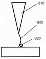
図1A、1B、1C、2,3,4、及び5を参照して、基板から粒子を取り除いてパッチに移送するための例示的なデバイスを説明する。図1Aから1Cは、本開示の態様による一連の表面相互作用時のデブリ除去デバイス1の一部の断面図を示す。基板3から粒子2を選択的に付着させてそれを軟質パッチ4に移転させることができる可能性のある一連の表面相互作用を図に示す(左から右へ移動する)。図1Aにおいて、粒子2は、(相対的に)高い表面エネルギー基板3を汚染し、これによりその表面エネルギーは減少して系全体におけるエントロピーが増加する。次に、図1Bにおいて、拡散的可動性の低表面エネルギーコーティングを備えたチップ5は、(同様に相対的に)高い表面エネルギー基板3及び粒子2をコーティングするようにされて、これらを剥離する。続いて、低表面エネルギー材料の喪失は、チップ5の表面エネルギーを僅かに増加させ(その通常の、非コーティング時の値に近づく)、剥離された粒子2をチップの表面6(更に、フッ化炭素などの材料は一般的に良好な結合力を有する)に付着させるためのエネルギー勾配が存在するようにすることができる。これらの相互作用はまた、特にチップ表面6が基板よりも清浄である場合には、系のエントロピーを増加させるはずである。最終的に、図1Cにおいて、粒子2は、軟質パッチ材料4内に機械的に詰め込まれ、この機械的動作はまた、低表面エネルギー材料でチップ表面6を再コーティングし、これによりエネルギーを減少させて系のエントロピーを増加させることになる。
1A, 1B, 1C, 2, 3, 4, and 5, exemplary devices for removing particles from a substrate and transferring them to a patch are described. 1A through 1C show cross-sectional views of a portion of debris removal device 1 during a series of surface interactions according to aspects of the present disclosure. The figure shows (moving from left to right) a possible series of surface interactions that can selectively adhere a
図2は、本開示の実施形態によるデブリ除去デバイス10の一部の断面図を示す。デバイス10は、低表面エネルギー材料のパッチ又はリザーバ13に隣接して位置決めされたナノスケールチップ12を含む。リザーバ内の低表面エネルギー材料は、固体、液体、半液体又は半固体とすることができる。
FIG. 2 shows a cross-sectional view of a portion of
チップ12上には、コーティング16が形成される。コーティング16を形成する前に、チップ12は、プレコーティング又は表面処理されて、チップ12の表面エネルギーを変える(例えば、毛細管、濡れ性、及び/又は表面張力の作用を変更する)ことができる。適切に選択されると、コーティング16によって、チップ12が非コーティングチップよりも長期間の間鋭利なままでいることが可能となる。例えば、PTFEコーティングのダイアモンドチップは、非コーティングダイアモンドチップよりも長い動作寿命を有することができる。
A
本開示の特定の態様によれば、コーティング16は、低エネルギー材料のパッチ又はリザーバ14内に見出されるのと同じ低表面エネルギー材料を含むことができる。また、本開示の特定の態様によれば、チップ12は、低エネルギー材料のパッチ又はリザーバ14と直接接触することができ、コーティング16は、低エネルギー材料のパッチ又はリザーバ14に対してチップ12を摩擦又は接触させることによって、チップ12の表面上に形成(又は補充)することができる。更に、低エネルギー材料のパッチ又はリザーバに対してチップ12を摩擦する及び/又はパッド14を引掻くことにより、チップ12の表面にわたって低表面エネルギー材料の表面拡散を強化することができる。
According to certain aspects of the present disclosure, coating 16 may include the same low surface energy material found within low energy material patches or
本開示の特定の態様によれば、コーティング16及び低エネルギー材料14のパッチ又はリザーバ14は共に、ポリテトラフルオロエチレン(PTFE)などの塩素化及びフッ素化された炭素含有分子、又はフッ素化エチレンプロピレン(FEP)などの他の類似材料で作製することができ、又は少なくともこれらを含むことができる。本開示の別の態様によれば、金属材料、酸化物、金属酸化物、又は他の何れかの高表面エネルギー材料の中間層15をチップ12の表面と低表面エネルギー材料コーティング16との間に配置することができる。中間層の代表的な実施例には、セシウム(Cs)、イリジウム(Ir)、及びこれらの酸化物(並びに塩化物、フッ化物など)を含むことができるが、これらに限定されない。これら2つの例示的な元素金属は、それぞれ低表面エネルギー及び高表面エネルギーを備えた比較的軟質の金属であり、従って、所与の汚染、基板、及び周囲環境に対して最適な表面エネルギー勾配の最適化を示す。加えて又は代替として、チップ12の表面を粗面化又はドープすることができる。高表面エネルギー材料又はチップ処理は一般的に、低表面エネルギー材料コーティング16をチップ12により強く固着するように作用する。チップの形状もまた局所的な表面エネルギー密度の変化(つまり、ナノスケールの鋭利さは、表面エネルギー密度をちょうど先端部で大きく増加させることになる)に影響を与えるので、チップ12の形状は、チップに対する粒子の選択的な付着力の増加をもたらすように変更することもできる。また、チップ12のチップ表面13を粗面化することにより、粒子及び多くの潜在的結合サイトとの接触表面積の増加(dA)に起因して、より大きな付着力をもたらすことができる。チップ表面13はまた、粒子又は一部の中間コーティングと反応して付着力を増加させることができる、極めて不安定で化学的に活性なダングリングボンドを含むように処理(場合によっては化学的又はプラズマプロセスによって)することができる。チップ表面13はまた、粒子と相互作用するチップ12の表面積を増大させるために、高密度炭素(HDC)又はダイアモンド状炭素(DLC)のような高表面積材料でコーティングすることができる。
According to certain aspects of the present disclosure, both the
高表面エネルギー前処理は、本開示の特定の態様による低表面エネルギーコーティング16無しで利用される。このような態様において、以下で検討する粒子20は、本明細書で検討するものと類似の方法を用いて他の何れかの軟質ターゲット(例えば、金、アルミニウム)に埋め込むことができ、或いはチップ12は、消耗品とすることができる。また、本開示を鑑みて当業者には理解されるように、他の物理的な及び/又は環境的なパラメータ(例えば、温度、圧力、化学作用、湿度)を変更して、チップ処理及び/又は粒子のピックアップ/ドロップオフを強化することができる。
A high surface energy pretreatment is utilized without a low
本開示の特定の態様によれば、図2及び3に示す構成要素の全てはAFMに含まれる。一部のこのような構成において、低エネルギー材料のパッチ又はリザーバ14は、実質的に平坦であり、基板18を支持するステージに取り付けられる。また、本開示の特定の態様によれば、低エネルギー材料のパッチ又はリザーバ14は、ステージから取り外し可能であり、容易に交換又は容易に補充可能とすることができる。例えば、低エネルギー材料のパッチ又はリザーバ14は、容易に取り外し可能なクランプ又は磁気マウント(図示せず)を用いてAFMに固定することができる。
According to certain aspects of the disclosure, all of the components shown in FIGS. 2 and 3 are included in the AFM. In some such configurations, the low energy material patch or
図3は、図2に示すデブリ除去デバイス10の別部分の断面図を示す。図3には、典型的には図2に示す低エネルギー材料のパッチ又はリザーバ14に隣接して位置決めすることができる基板18が示される。また図3には、基板18の表面に形成されたトレンチ22に存在することができる複数の粒子20が示される。粒子20は、典型的には、ファンデルワールス近距離力によってトレンチ22の表面に付着する。図3において、チップ12を基板18に隣接するよう移動させて位置決めし、粒子20をチップ12に物理的に付着させることができる。トレンチ22の底部に到達させるために、図2及び3に示すようなチップ12は、高アスペクト比のチップとすることができる。トレンチ22は、図3に示されるが、粒子20は、洗浄されることになる別の構造上に付着し、又は見出すことができる。
FIG. 3 shows a cross-sectional view of another portion of the
図4は、図2に示すデブリ除去デバイス10の一部分の断面図を示し、ここで粒子20は、低エネルギー材料のパッチ又はリザーバ14の表面内に又は表面に対してチップ12を延ばすことによって、チップ12から移送することができ、また、低エネルギー材料のパッチ又はリザーバ14に埋め込むことができる。その後、図5の断面図に示すように、チップ12を後退させて、チップ12がもはや低エネルギー材料のパッチ又はリザーバ14と接触しないようにすることができる。チップ12が低エネルギー材料のパッチ又はリザーバ14から後退又は引き出されると、その前にチップ12上にあった粒子20は、低エネルギー材料のパッチ又はリザーバ14と共に留まる。
FIG. 4 shows a cross-sectional view of a portion of the
本開示の特定の態様によれば、図2-5に示すデバイス10は、デブリ除去方法を実施するのに利用することができる。本開示の特定の態様は、本明細書で検討する方法の前に又はこれに従って他の粒子洗浄プロセスと併せて用いることができる点に留意されたい。更に、粒子、デブリ、又は汚染物質という用語は、基板表面に対する異物を記述するのに同義的に用いることができる点に留意されたい。また、1つのチップ12だけが検討され図示されているが、複数のチップを同時に用いて複数の構造体から同時に粒子を除去してもよい点に留意されたい。更に、複数のチップを本明細書にて検討する方法にて並行して同時に使用してもよい。
According to certain aspects of the present disclosure, the
上述のデブリ除去方法は、図3の基板18上に存在するように示された粒子20(すなわち、デブリの断片)の1又は2以上に隣接してチップ12を位置決めするステップを含むことができる。本方法は更に、同様に図3に示されるように粒子20をチップ12に物理的に付着させるステップ(静電気的に付着させるステップではなく)と共に、粒子(又は複数の粒子)20及び周囲の表面と接触したときのチップ12の何らかの実施可能な繰り返し動作を含むことができる。粒子20のチップ12への物理的な付着の後、本方法は、図4に示すように、チップ12を基板18から離れて移動及び/又は引き出して、チップ12を粒子20と共に低エネルギー材料のパッチ又はリザーバ14に移動させることによって、粒子20を基板18から除去するステップを含むことができる。
The debris removal method described above may include positioning the
本開示の特定の態様によれば、本方法は、チップ12の少なくとも一部分上にコーティング16を形成するステップを含むことができる。本開示の特定の態様によれば、コーティング16は、基板18の表面エネルギーよりも低い表面エネルギーを有するコーティング材料を含むことができる。加えて又は代替として、コーティング16は、基板18と接触状態にある粒子20の表面積よりも大きい表面積を有するコーティング材料を含むことができる。
According to certain aspects of the present disclosure, the method may include forming
上記に加えて、本方法の一部の態様は更に、チップ12が粒子又はデブリの別の断片(図示せず)に隣接して、粒子又はデブリの別の断片がチップ12に物理的に付着するように、基板18の少なくとも第2の位置にチップ12を移動させるステップを含むことができる。粒子又はデブリの別の断片は、その後、図4に示すものと同様の方法で、基板18からチップ12を離れて移動させることにより基板18から除去することができる。
In addition to the above, some aspects of the present method further include placing the
デブリ(例えば上述の粒子20)が基板18から除去されると、本開示による幾つかの方法は、基板から離れて位置決めされた材料片(例えば、上述の低エネルギー材料のパッチ又はリザーバ14)にデブリの断片を堆積させるステップを含むことができる。
Once the debris (e.g.,
チップ12は、大量のデブリを除去するために繰り返し使用することができるので、本開示の特定の態様によれば、本方法は、低エネルギー材料のパッチ又はリザーバ14にチップ12を押し込むことによってコーティング16を補充するステップを含むことができる。低エネルギー材料のパッチ又はリザーバからの低表面エネルギー材料は、経時的にチップ12のコーティング16において生じる可能性がある何らかの孔又はギャップをコーティングすることができる。この補充ステップは、低エネルギー材料のパッチ又はリザーバ14内にチップ12を押し込んだ後、低エネルギー材料のパッチ又はリザーバ14内でチップ12を横方向に移動させるステップ、チップ12の表面を摩擦するステップ、又はチップ12及び/又は低エネルギー材料のパッチ又はリザーバ14の物理的なパラメータ(例えば、温度)を変更するステップのうちの1又は2以上を伴うことができる。
Because the
本開示による特定の方法は、修復が完了した後に除去された材料が塊になって再度基板に強く付着する可能性を低減するために、修復前に欠陥又は粒子の周りの小領域を低表面エネルギー材料に曝すステップを含むことができる点に留意されたい。例えば、欠陥/粒子及び欠陥周りのおよそ1~2ミクロン領域は、本開示の特定の態様に従ってPTFE又はFEPでプレコーティングすることができる。このような場合には、低表面エネルギー材料でコーティングされ又は構成されたチップ12(例えば、PTFE又はFEPのチップ)を用いて、他の修復ツール(レーザ、電子ビーム)が利用中の場合でも極めて多くの低表面エネルギー材料を修復領域に付与することができる。チップ12上のコーティング16に加えて、チップ12の一部又は全部は、限定ではないが、塩素化及びフッ素化炭素含有分子などの低エネルギー材料を含むことができる。このような材料の実施例には、PTFE又はFEPを含むことができる。加えて又は代替として、金属及びその化合物などの他の材料を用いてもよい。一部の代表的な実施例には、Cs、Ir、及びこれらの酸化物(並びに塩化物、フッ化物など)が含まれる。これら2つの例示的な元素金属は、それぞれ低表面エネルギー及び高表面エネルギーを有する比較的軟質の金属であり、従って、所与の汚染物質、基板、及び周囲環境に対して最適な表面エネルギー勾配の最適化を示す。加えて又は代替として、他の炭素系化合物を用いてもよい。一部の代表的な実施例には、HDC又はDLCが含まれる。
Certain methods according to the present disclosure reduce the likelihood that removed material will agglomerate and strongly adhere to the substrate again after the repair is complete by reducing the small area around the defect or particle to a low surface prior to repair. Note that the step of exposing to an energetic material can be included. For example, the defect/particle and the approximately 1-2 micron area around the defect can be pre-coated with PTFE or FEP according to certain aspects of the present disclosure. In such cases, using a
本開示の特定の態様によれば、本方法は、粒子をチップ12の先端から該先端の上部でチップ12を支持するAFMカンチレバーアーム(図示せず)に向けて押し進めるために低エネルギー材料のパッチ又はリザーバ14を用いるステップを含む。このような粒子20の押し上げは、チップ12の先端付近にスペースを確保して、より多くの粒子20を物理的に付着させることができる。
According to certain aspects of the present disclosure, the method uses a patch of low energy material to push particles from the
本開示の特定の態様によれば、チップ12を低エネルギー材料のパッチ又はリザーバ14に見出すことができる軟質材料のパレット内に交互に浸漬、挿入、及び/又は窪み形成することによって、例えば基板18のトレンチ22などの高アスペクト比構造からナノ加工デブリを除去するためにチップ12が使用される。選ばれた態様において、低エネルギー材料のパッチ又はリザーバ14の軟質材料は、柔らかい又は展性のある粘稠性を有することができる。この軟質材料は一般に、それ自体よりもチップ12及び/又はデブリ物質(例えば、粒子20内の)に対してより優れた付着力を有することができる。軟質材料はまた、ナノ加工のデブリ粒子20をチップ12に静電気的に吸着する極特性を有するように選択することができる。例えば、低エネルギー材料のパッチ又はリザーバ14は、可動性界面活性物質を含むことができる。
According to certain aspects of the present disclosure, chips 12 are alternately dipped, inserted, and/or recessed into a palette of soft materials that may be found in patches or
上記に加えて、本開示の特定の態様によれば、チップ12は、1又は2以上の誘電性表面(すなわち、電気絶縁性表面)を含むことができる。これらの表面を特定の環境条件(例えば、低湿度)下で類似の誘電性表面上で摩擦させ、静電気的表面帯電に起因する粒子ピックアップを可能にすることができる。また、本開示の特定の態様によれば、コーティング16は、限定ではないが、水素結合、化学反応、強化表面拡散を含むことができる、他の何れかの近距離機構によって粒子を吸着することができる。
In addition to the above, according to certain aspects of the present disclosure,
次に、図6-11を参照しながら、デブリ除去チップの例示的な態様を説明する。低エネルギー材料のパッチ又はリザーバ14の軟質パレット材料を貫通する(すなわち、窪み形成する)のに十分な程度に強固で剛性のある何れかのチップを使用することができる。従って、極めて高いアスペクトのチップ外形形状(1:1を超える)は、本開示の範囲内にある。チップが軟質の(場合によっては粘着性の)材料を貫通するほどに十分に剛性があれば、強固で可撓性のある高アスペクト比のチップが、より脆弱及び/又は可撓性が小さいチップに優先して一般に選択される。従って、本開示の特定の態様によれば、チップは、トレンチ22又は基板18への損傷又は変化無しに、基板18の修復トレンチ22の側部及び角部に摩擦することができる。この作業の大まかなマクロスケール類似物は、深い内径内を移動する剛性のあるブリストルである。本開示の特定の態様によれば、以下でより詳細に説明するように、チップ12は、複数の堅固な又は剛性のあるナノフィブリル・ブリストルを備えることができる点に留意されたい。図6に示すような一態様において、複数の堅固な又は剛性のあるナノフィブリル・ブリストル30の各ブリストルは、チップ12から直線的に延びることができる。一態様において、複数の堅固な又は剛性のあるナノフィブリル・ブリストル30は、カーボンナノチューブ、金属ウィスカなどで形成することができる。加えて又は代替として、以下でより詳細に説明するように、チップ12は、複数の可撓性又は巻き付けナノフィブリルを備えることができる。複数の可撓性又は巻き付けナノフィブリルは、例えば、高分子材料を用いてチップ12上に形成することができる。当然ながら、他の材料及び構造も企図される。
Exemplary aspects of debris removal tips will now be described with reference to FIGS. 6-11. Any tip that is strong and rigid enough to penetrate (ie, dimple) the soft pallet material of the
本開示の特定の態様によれば、1又は2以上の粒子がピックアップされたか否かの検出は、関心領域(ROI)のナノコンタクトAFMスキャンを用いて粒子を検出することによって実施することができる。チップ12は次に、ターゲットでの後処理まで再スキャンすることなく、基板18から後退することができる。しかしながら、チップ12によってピックアップされたデブリ物質の総質量もまた、チップの共振周波数の相対的シフトによりモニタすることができる。更に、他の動力学を同じ機能に使用してもよい。
According to certain aspects of the present disclosure, detecting whether one or more particles have been picked up can be performed by detecting particles using nanocontact AFM scanning of a region of interest (ROI). .
上述のように及び図5に示すように粒子20を取り除くために軟質材料内に窪み形成する代わりに、チップ12を低エネルギー材料のパッチ又はリザーバ14内に誘導し、粒子20を取り除くことができる。従って、チップが意図せずに粒子20をピックアップした場合、粒子20は、別の修復を行うことによって取り除くことができる。特に誘導によって粒子20を堆積するために異なる材料が使用される場合、金箔などの軟質金属を利用することができる。
Instead of recessing into the soft material to dislodge
上記に加えて、紫外(UV)光硬化材料、又は同様に化学的非可逆反応を受けやすい他材料を使用して、チップ12をコーティングする、並びにコーティング16を形成することができる。UV硬化の前に、材料は、基板18から粒子20をピックアップする。チップ12が基板18から取り外されると、チップ12は、UV光源に曝すことができ、この場合、材料特性を変化させて粒子20のチップ12に対する付着力を低下させ、且つ低エネルギー材料のパッチ又はリザーバ14中の材料に対する付着力を高めることになり、その後、粒子20をチップ12から取り除いて低エネルギー材料のパッチ又はリザーバ14と共に堆積することができる。当然ながら、粒子のピックアップ及び除去の選択性を強化又は可能にする他の非可逆プロセスも企図される。
In addition to the above, ultraviolet (UV) light curable materials, or other materials that are similarly susceptible to irreversible chemical reactions, can be used to
本開示の特定の態様は、様々な利点を提供する。例えば、本開示の特定の態様は、極めて高いアスペクトのAFMチップ外形形状(1:1を超える)を用いて高アスペクトのトレンチ構造から能動的なデブリ除去を可能にする。また、本開示の特定の態様は、極めて高いアスペクトのチップを使用すること並びにAFMオペレータによって現在使用されているソフトウェア修復シーケンスに比較的軽微な調整を行うことに加えて、低表面エネルギー又は軟質材料パレットをAFMに取り付けることによって比較的容易に実施することができる。更に、本開示の特定の態様によれば、他のいかなる方法によっても洗浄できないマスクの表面から粒子を選択的に除去するのに使用することができる(ナノピンセットのように)新規のナノ加工ツールを実施することができる。これは、デブリが最初に非コーティングのチップで表面から取り出され、次にコーティングされたチップでピックアップされる、より従来的な修復と組み合わせることができる。 Certain aspects of the disclosure provide various advantages. For example, certain aspects of the present disclosure enable active debris removal from high aspect trench structures using very high aspect AFM tip geometries (greater than 1:1). Also, certain aspects of the present disclosure, in addition to using extremely high aspect tips and making relatively minor adjustments to the software inpainting sequences currently used by AFM operators, are suitable for low surface energy or soft materials. It can be done relatively easily by attaching a pallet to the AFM. Further, according to certain aspects of the present disclosure, novel nanofabrication tools (like nanotweezers) that can be used to selectively remove particles from the surface of masks that cannot be cleaned by any other method. can be implemented. This can be combined with more conventional remediation where debris is first removed from the surface with an uncoated tip and then picked up with a coated tip.
一般に、低表面エネルギー材料は上述の局所的な洗浄方法で使用されるが、他の実施可能な変形形態もまた、本開示の範囲内であることに留意すべきである。典型的には、これらの変形形態は、粒子20をチップ12に引き付ける表面エネルギー勾配(すなわち、ギブズ自由エネルギー勾配)を生成し、その後で、他の何らかの処理により反転されて粒子20をチップ12から放出することができる。
It should be noted that while low surface energy materials are generally used in the topical cleaning methods described above, other possible variations are also within the scope of the present disclosure. Typically, these variations create a surface energy gradient (i.e., a Gibbs free energy gradient) that attracts
本開示の一態様は、高アスペクト構造内での能力を向上させると同時に下にある基板に対して機械的により攻撃的でないプロセスを可能にするために、AFMチップの作用端に少なくとも1つのナノフィブリルの取り付けを伴う。これらのフィブリルは、その機械的特性及びナノ粒子洗浄に向けた適用に応じて、2つの異なるラベル、すなわち「剛性のある」フィブリルと「巻き付け」フィブリルに分類することができる。この相違点を理解するために、図7A及び7Bは、これら2つのタイプのフィブリル、すなわち、チップ710に取り付けられた剛性フィブリル700とチップ760に取り付けられた巻き付けフィブリル750とを示す。更に、ビットクリーン(BitClean)粒子洗浄において必要とされる2つの重要なプロセス:ナノ粒子の取り出し、汚染表面からナノ粒子の付着及び抽出を最初に理解しなければならない。これらの定められた最重要ステップに関して、2つの異なるフィブリル間の機能的な相違点は、以下のように示される。
One aspect of the present disclosure is to provide at least one nanostructure at the working end of the AFM tip to improve performance within high aspect structures while enabling processes that are mechanically less aggressive to the underlying substrate. Accompanied by the attachment of fibrils. These fibrils can be classified under two different labels, 'rigid' fibrils and 'wound' fibrils, depending on their mechanical properties and their application towards nanoparticle cleaning. To understand this difference, FIGS. 7A and 7B show these two types of fibrils:
図7Aに関連して、剛性フィブリル700は、ナノ粒子を取り出すためにフィブリル自体の機械的動作及び機械的強度により多く依存する。従って、破断することなく首尾よく取り出しを達成するために、剪断及び曲げ強度及び弾性率にも依存している。これは、単結晶ダイアモンドの強度及び剛性(典型的には硬度と呼ばれる)を超える又は適合することができる材料が僅かであることを意味する。これらの中には、カーボンナノチューブ及びグラフェンがあり、これは、共にダイアモンドでも見出される炭素-炭素sp3混成軌道原子間結合(既知の最強結合の1つ)を用いていることに起因する。他の企図される材料には、場合によってはダイアモンドの機械的強度及び剛性を超えることができる特性を有するホウ素含有化学物質の特定相が含まれ、これらを用いることもできる。一般に、多くの物質(ダイアモンドを含めて)は、その次元が縮退されると、本質的により強固でより剛性が高くなることができる(構造が原子スケールに近づき、その形状が熱拡散挙動によって決定付けられるにつれて、剛性は低下する)。これは、最初にナノ結晶性金属で観察されたが、分子シミュレーション及び単結晶ナノピラーに関しても生じる一部の実験でも確認されている物質現象である。この挙動に対する1つの有力な仮説は、塑性変形の欠陥拡散機構につながる。より大きなスケールでは、これらの結晶欠陥(空孔、転位など)は、バルク支配型動力学において拡散し相互作用する。より小さなスケールでは(物質及び温度など全てが同じ場合)、これら欠陥の動きは、結晶のバルクにおけるよりも遥かに高い表面拡散型動力学に支配されるようになると考えられる。物質連続体近似の範囲内で考えると、この大きな表面拡散速度は、結果的に低応力レベルでの物質の塑性変形(降伏とも呼ばれる)及び破損にもつながる。例えば、Tiの単結晶ナノピラーに関して、降伏応力は、約8~14nmの範囲までは断面幅の減少と共に増加することが明らかになっているが、この範囲未満では、その挙動は、降伏応力が断面幅の減少と共に実際には減少する変曲点を経る。
With reference to FIG. 7A,
図8Aから8Cは、AFMチップ810の先端又はその近くに取り付けられた単一の剛性フィブリル800を用いてターゲット基板からナノ粒子を取り出して取り除く例示的なプロセスを示す。チップ810は表面に接近し、剛性フィブリル無しでAFM走査と同じ原理を用いて走査する。チップ810の先端に取り付けられた単一の剛性フィブリルを考慮して、異なる操作パラメータが適用可能であることは、当業者には理解されるであろう。粒子が位置特定されると、チップ810は表面830に向けて移動され、剛性フィブリル800は、図8Bに概略的に示されるように弾性変形する。一態様において、剛性フィブリル800の変形は、圧縮性、剪断性、曲げ性、引張性、又はこれらの組み合わせとすることができ、表面830からナノ粒子820を機械的に取り出すのに使用することもできる。ナノ粒子820が取り出されると、剛性フィブリル800、基板840及びナノ粒子820の表面間の表面エネルギー及び面積の相違が、後でナノ粒子820が基板表面から抽出されたときに剛性フィブリル820に付着するかどうかを決定付ける。
8A-8C show an exemplary process of extracting and removing nanoparticles from a target substrate using a single
これに対しての剛性フィブリルのナノ粒子洗浄プロセスに特有の例外は、図9Aから9Cに示すように、2又は3以上の剛性フィブリルが、ナノ粒子の直径よりも小さい(しかし、これらの剪断及び曲げ弾性率及び幅に対する長さの比によって決定されるような、剛性フィブリルに対する弾性変形限界より小さくはない)距離でチップ表面に強固に取り付けられている場合である。2又は3以上の剛性フィブリル900a、900bがナノ粒子の直径よりも小さい距離でチップ910に取り付けられた態様によれば、そのシーケンスは、図8Aから8Cに関して上述されたような単一の剛性フィブリルと極めて類似している。その相違点は、図9Bに概略的に示すように、ナノ粒子920の周りにより歪んだ又は変形した剛性フィブリル900a、900bが存在するという観察に始まり、これによって、1又は2以上の剛性フィブリル900a、900bが所与の洗浄シナリオに対してナノ粒子920を取り出すのに必要となるような方式(力及び加えられる力の角度)でナノ粒子に衝突する確率が増大する。取り出しステップの後に、マルチフィブリルチップ910は、粒子920が付着する(すなわち、濡れる)より多くの潜在的表面積を有することができる。チップ910が基板から後退すると、図9Cに概略的に示されるように、フィブリルの長さ及び間隔が適正範囲にある場合には別の相違点が現れる。この設定に対するナノ粒子920は、剛性のあるナノフィブリル900a、900b間のスペース内に機械的にトラップされる可能性があり、これにより、マルチフィブリル900a、900bへの付着力の増大と、基板表面930からナノ粒子920を取り出す確率の増大とをもたらすことができる。同様に、別の表面上にナノ粒子920を堆積させることが望まれしい場合には、チップ910を表面に再接近させて、剛性フィブリル900a、900bにナノ粒子920の機械的な捕捉を緩めるように再び応力を加え、これにより、ナノ粒子920が所望の表面位置に堆積される確率を高めることができる。上述のように、これは、フィブリル900a、900bの長さ及び間隔が適正範囲内にあると仮定しており、1次モデルにおいて、本開示を鑑みて当業者には理解されるように、これらの範囲には、ナノ粒子920(砕けることのない強固なナノ粒子を仮定している)の最小幅より小さいが、フィブリル900a、900bがその剪断及び曲げ強度の限界(フィブリルの相対的な長さによっても決まり、フィブリル取り付けの付着強度がこの限界より小さいと仮定している)を超えて曲がることのない程度に大きいフィブリル間隔が含まれる。選ばれた態様において、2又は3以上の剛性フィブリルは、種々の等しくない長さを有することができる。
The exception specific to the rigid fibril nanoparticle washing process to this is that two or more rigid fibrils may be smaller than the nanoparticle diameter (but their shear and rigidly attached to the chip surface at a distance not less than the elastic deformation limit for rigid fibrils, as determined by the flexural modulus and length to width ratio. According to embodiments in which two or more
剛性フィブリルとは何か(巻き付けフィブリルと対照的に)を定義するために、特定の物質及びナノ構造に対して非等方的なバネ定数(有効剪断及び曲げ弾性率に関係する)を定めることができなければならない。これは実際に行うことが極めて難しいので、本明細書においては、これらの特性は、おおよそ引張(別名ヤングの)弾性率及び強度に比例すると仮定する。引張弾性率は、物質が弾性的な(すなわち、バネ様の)機械的特性を示す応力範囲内での物質の剛性の実施可能な尺度である。これは、応力を歪みで除算することによって与えられ、従って、応力と同じ単位となる(歪みは、初期寸法に対する最終寸法の変形率として定義されるため)。引張弾性率は、特に剛性を定義しないが、フィブリルは、それ自体が破断して付加的な汚染を基板表面に生成することなく、ナノ粒子を取り出すのに十分な力を加えることができる必要があるので、引張強度もまた重要である。強度も応力の単位(パスカル)で与えられる。ダイアモンドに関して、その固有の引張弾性率は、およそ1.22テラパスカル(TPa)で、引張強度は8.7~16.5ギガパスカル(GPa)に及び、本明細書では剛性及び強度に対する一般的基準尺度を提供する(引張弾性率が0.5TPaのタングステンに対する値内に近く、又はこれらの値を超える)。カーボンナノチューブは、その性質上、真性の実体ではないので、これらの引張弾性率は、個々の分子及びその特性に特有である(例えば、単層又は多層、それぞれSWNT又はMWNT、キラリティなど)。SWNTに関して、その引張弾性率は、1~5TPaに及び、その引張強度は13~53GPaに及ぶことができる。この範囲にある別の部類の物質と比較するため、BxNy(様々な化学量論組成の窒化ホウ素化合物)は、0.4~0.9TPaに及ぶ引張弾性率を有する。巻き付けフィブリルと剛性フィブリルを区別してその境界を定めるために、最も適切で適用可能な標準的な機械的材料特性は、降伏応力である。剛性フィブリルは、0.5GPa(1GPa=1x109N/m2)以上の降伏応力を有する材料としてここでは定義される。従って、消去法により、0.5GPa未満の降伏応力を有する何れかの材料は、巻き付けフィブリルと見なすことになる。特にナノスケールにおいて、多くの物質は非等方的な機械的特性を示すことができ、よって降伏応力は、フィブリルの主要(すなわち、最長)寸法を横切る剪断応力(又は等価な曲げ応力)として規定されることが重要である点に留意されたい。 Defining anisotropic spring constants (related to effective shear and flexural moduli) for specific materials and nanostructures to define what rigid fibrils are (as opposed to wound fibrils) must be able to Since this is very difficult to do in practice, we assume here that these properties are roughly proportional to tensile (aka Young's) modulus and strength. Tensile modulus is a feasible measure of a material's stiffness within the stress range over which the material exhibits elastic (ie, spring-like) mechanical properties. It is given by dividing the stress by the strain and is therefore in the same units as the stress (because strain is defined as the ratio of final dimension to initial dimension). Tensile modulus does not specifically define stiffness, but the fibrils must be able to apply sufficient force to eject the nanoparticles without rupturing themselves and creating additional contamination on the substrate surface. , tensile strength is also important. Intensity is also given in units of stress (pascals). For diamond, its intrinsic tensile modulus is approximately 1.22 terapascals (TPa) and tensile strength ranges from 8.7 to 16.5 gigapascals (GPa); Provide a reference scale (close to within or above values for tungsten with a tensile modulus of 0.5 TPa). Since carbon nanotubes are by nature not intrinsic entities, their tensile modulus is specific to the individual molecule and its properties (eg, single-walled or multi-walled, SWNT or MWNT, respectively, chirality, etc.). For SWNTs, their tensile modulus can range from 1 to 5 TPa and their tensile strength can range from 13 to 53 GPa. To compare with another class of materials in this range, B x N y (boron nitride compounds of various stoichiometries) have tensile moduli ranging from 0.4 to 0.9 TPa. The most relevant and applicable standard mechanical material property to distinguish and demarcate winding fibrils from rigid fibrils is yield stress. A rigid fibril is defined herein as a material with a yield stress of 0.5 GPa (1 GPa=1×10 9 N/m 2 ) or higher. Therefore, by process of elimination, any material with a yield stress of less than 0.5 GPa would be considered a wound fibril. Especially at the nanoscale, many materials can exhibit anisotropic mechanical properties, so the yield stress is defined as the shear stress (or equivalent bending stress) across the major (i.e., longest) dimension of the fibril. Note that it is important that
巻き付けフィブリルは、剛性フィブリルとは対照的に、十分に高い(同等の)引張強度と共に遥かに小さなバネ定数を有することになる。巻き付けフィブリルの場合、適用方法の相違に起因して、基板表面からナノ粒子を取り出して抽出するために引張力が加えられるので、引張強度はその性能に直接的に関係する。しかしながら、文献で引用されるほとんどの機械的特性は、原則として、単分子フィブリル(又は、単分子スケールに近いナノスケールフィブリル)に対する引張特性にはほとんど完全に無関係なバルク物質に関するものである点に留意されたい。例えば、PTFEは通常、バルク物質では極めて低い引張弾性率及び強度を有する(それぞれ、0.5GPa及び場合によっては<<20MPa)とされるが、分子の骨格が炭素-炭素sp混成軌道化学結合から構成されるので、その単分子の引張強度は、他の多くの物質、カーボンナノチューブ及びグラフェン(これらの全ては、同種の化学結合を含む)よりもダイアモンドに匹敵するはずである。バルク物質の機械的特性は、その近傍と相互作用する単一分子鎖の作用により関連するので、凝集力のある単分子の曲げ及び剪断弾性率の両方に匹敵するはずである。これらのタイプの物質(高分子)は、塑性変形と関係した機械的特性の例証となるので、これらの分子は、高い可撓性を示すより拡散性熱的挙動に従って変形すると予期される。剛性フィブリルに対する巨視的な例示が、ガラスの細片である場合、巻き付けフィブリルの相当する例示は、薄い炭素繊維となる(後者は、高い引張強度と共にマクロスケールで高い可撓性を有するように見える)。 Wound fibrils will have a much smaller spring constant with a sufficiently high (comparable) tensile strength as opposed to rigid fibrils. In the case of wound fibrils, tensile strength is directly related to their performance, as tensile forces are applied to lift and extract the nanoparticles from the substrate surface due to differences in application methods. However, most mechanical properties cited in the literature relate in principle to bulk materials that are almost completely irrelevant to tensile properties on monomolecular fibrils (or near-monomolecular-scale nanoscale fibrils). Please note. For example, PTFE is typically assumed to have very low tensile modulus and strength in bulk materials (0.5 GPa and sometimes <<20 MPa, respectively), but the molecular backbone is As such, its single-molecule tensile strength should be more comparable to diamond than many other materials, carbon nanotubes and graphene, all of which contain similar chemical bonds. The mechanical properties of bulk materials are related by the action of single-molecule chains interacting with their neighbors and should therefore be comparable to both the flexural and shear moduli of cohesive single molecules. Since these types of materials (polymers) demonstrate mechanical properties associated with plastic deformation, these molecules are expected to deform according to a more diffusive thermal behavior exhibiting high flexibility. If the macroscopic example for rigid fibrils is a strip of glass, the comparable example for wound fibrils would be thin carbon fibers (the latter appearing to have high flexibility at the macroscale along with high tensile strength). ).
図10A~10Cは、本開示の一態様による、先端近く又は先端にてAFMチップ1010に取り付けられた巻き付け(可撓性)ナノフィブリル1000を用いたナノ粒子洗浄シーケンスを示す。巻き付け型フィブリル1000を変形させるのに必要な圧縮応力がないので、近距離表面エネルギー力によりフィブリル1000がナノ粒子表面に付着することが可能となる程にフィブリル1000をナノ粒子表面に接近させるために、チップ1010は、表面1030の近接近される。フィブリル1000、ナノ粒子1020、及び基板表面1030の相対的表面エネルギーは、フィブリルが優先的にナノ粒子表面に付着するように標的化されるので、フィブリル1000が、フィブリル長さを考慮した十分な弛みを有して接触状態になると、フィブリル1000が粒子1020に巻き付くのを可能にするために、時間及び付与される撹拌エネルギー(場合によっては機械的及び/又は熱的なエネルギー)だけが必要とされる。より剛性のあるチップからの機械的なエネルギー(フィブリル1000が取り付けられたチップ1010か、又は前の処理パスの別のチップによるかを問わず)が加えられて、最初に粒子1120を取り出すことができる。フィブリル1000がナノ粒子1020に十分に巻き付くと、図10に概略的に示されるように、チップ1010は次に、基板表面1030から後退する。この段階の間、フィブリル1000のナノ粒子1020への付着力(ナノ粒子の周りに巻き付いて絡まるほど強化される)、フィブリル1000の引張強度、及びAFMチップ1010に対するその付着力が全て、ナノ粒子1020の基板1040に対する付着力よりも大きい場合には、ナノ粒子1020は、図10Cに概略的に示されるように、基板1040から後退することになる。
10A-10C show a nanoparticle cleaning sequence with wrapped (flexible) nanofibrils 1000 attached to an
ナノ(又は分子)スケールの巻き付けフィブリルを作製するのに用いることができる実施可能な材料の幾つかの実施例には、RNA/DNA、アクチン、アミロイドのナノ構造、及びイオノマーが含まれる。RNA(リボ核酸)及びDNA(デオキシリボ核酸)は、類似の化学的性質、調製、及び処理プロセスを示すので、一緒に説明する。近年、俗に「DNAオリガミ」として知られる技術に関して大幅な進歩が成し遂げられ、これにより、DNA分子を結合する方法の精密な化学工学が可能となる。これら又は類似の化学的性質に適用される類似のプロセスは、長鎖高分子が脱離して、列状に結合することができると考えられる。最も一般的なプロセスを考慮すると、特定のDNA配列は、化学的に生成され又は周知の一本鎖ウィルスDNA配列から商業的に得られることになり、適切に化学的官能化された(化学力顕微鏡法の実施で行われるように)AFMチップ1110は、DNA配列を含んだ水溶液に浸漬され又は表面に対しAFM接触状態にされて、DNA配列が設計どおりに結合するようになる。チップ1110は次に、図11A~11Dに示すように、基板表面1130から粒子除去のために官能化することができる。図中で左から右へ移動すると、官能化されたチップ1110は、図11Aに示すように、粒子1120及び基板表面1130に接近する(DNA鎖1100の長さよりも近接して)ように移動又は作動させることができる。チップ1110が、図11Bに示すように取り出された粒子1120の近くにある間、活性化化学的性質(商業的にも入手可能なヘルパーDNA鎖か、又はマグネシウム塩などの他の幾つかのイオン活性剤)を有してより高い温度(おそらく~90℃)を付与することができる。次いで、環境が冷却され(おそらく~20℃まで)、鎖1100における目標の配列が図11Cに示すように結合することができる(結合鎖1100は、分子の自由両端部にある)。ナノ粒子1120が確実に付着する点にDNAコーティング1100が凝固すると、図11Dに示すように、基板表面1130からチップ1110を抽出することができる。これらの小スケールでは、ナノ粒子とチップ間のこの結合は機械的と言えるが、粒子が分子スケールの場合には、立体結合として説明することもできる。立体効果は、十分に近接近した原子の反発力によって生成することができる。原子又は分子が、全ての実施可能な拡散方向で原子によって囲まれている場合には、効果的に捕捉されて、その周囲に他の何れかの原子又は分子と化学的又は物理的に相互作用することができないことになる。本開示を鑑みて当業者には理解されるように、RNAも同様に操作することができる。
Some examples of possible materials that can be used to fabricate nano (or molecular) scale winding fibrils include RNA/DNA, actin, amyloid nanostructures, and ionomers. RNA (ribonucleic acid) and DNA (deoxyribonucleic acid) are described together as they exhibit similar chemical properties, preparation and processing processes. In recent years, great strides have been made in the technology colloquially known as "DNA origami", which allows for the precise chemical engineering of how DNA molecules are joined together. Similar processes applied to these or similar chemistries would allow long-chain macromolecules to detach and attach in series. Given the most common process, a specific DNA sequence would be chemically generated or commercially obtained from known single-stranded viral DNA sequences and appropriately chemically functionalized (chemically functionalized). The
次に実施可能な巻き付けナノフィブリルの候補は、真核細胞中にフィラメントを形成する類似した球状の多機能タンパク質のファミリーであり、その1つはアクチンとして知られる。アクチンは、骨組み形成、定着、機械的支持、及び結合のために細胞内部で使用され、このことは、高度に適応可能で十分に強固なタンパク質フィラメントであることを示している。アクチンは、上述のDNAオリガミ関連プロセスと極めて類似した方法で適用され使用されることになる。実験により、このタンパク質が6.7x4.0x3.7nmの寸法の分子に結晶化可能であることが示された。 The next viable wrapped nanofibril candidate is a family of similar globular multifunctional proteins that form filaments in eukaryotic cells, one of which is known as actin. Actin is used inside cells for scaffold formation, anchorage, mechanical support, and binding, indicating that it is a highly adaptable and sufficiently rigid protein filament. Actin will be applied and used in a manner very similar to the DNA origami-related processes described above. Experiments have shown that this protein can be crystallized into molecules with dimensions of 6.7×4.0×3.7 nm.
特定の海洋生物(フジツボ、藻類、海洋扁形動物など)が広範囲の基質材料にバイオミメティックス的に(又は直接的に)強固に結合できる機構の研究は、別の巻き付けフィブリル候補を提供する。これらの海洋生物は、一般に頭文字語DOPA(3、4-ジヒドロキシフェニルアラニン)と呼ばれる物質を分泌し、これは機能性アミロイドナノ構造でこれらの基質表面に結合する。アミロイド分子の付着特性は、フィブリル軸に対して垂直に配向されて高密度の水素結合網を通じて連結されたβ鎖に起因する。この結合網は、何千もの分子単位にわたって連続的に広がることが多い超分子βシートをもたらす。このようなフィブリル状ナノ構造は、水中付着、環境悪化に対する耐性、自己重合による自己修復、及び広大なフィブリル表面積を含む、幾つかの利点を有する。先に検討したように、広大なフィブリル表面積は、フジツボの付着性プラークにおける接触面積の増加により付着力を高める。アミロイドのナノ構造はまた、汎用アミロイド分子間βシート構造と関係した凝集強度及びアミロイドコアの外部の付着性残基に関連した付着強度などの、実施可能な機械的利点を有する。これらの特性により、アミロイド構造は広範囲の用途において有望な新世代の生体発想型接着剤の基礎とされる。分子自己組織化の利用の進歩により、ナノテクノロジー上の応用のために合成アミロイド及びアミロイド類似性接着剤の生成が可能となったが、1つには、基礎を成す生物学的設計原理を理解する上での限界に起因して、完全に合理的な設計が未だ実験的に示されていない。 Investigation of the mechanisms by which certain marine organisms (barnacles, algae, marine flatworms, etc.) can bind tightly biomimetically (or directly) to a wide range of substrate materials provides another winding fibril candidate. These marine organisms secrete a substance commonly referred to by the acronym DOPA (3,4-dihydroxyphenylalanine), which binds to their substrate surfaces in functional amyloid nanostructures. The adhesive properties of amyloid molecules are attributed to β-strands oriented perpendicular to the fibril axis and linked through a dense network of hydrogen bonds. This network of connections leads to supramolecular β-sheets that often extend continuously over thousands of molecular units. Such fibril-like nanostructures have several advantages, including adhesion in water, resistance to environmental degradation, self-healing by self-polymerization, and large fibril surface area. As previously discussed, the large fibril surface area enhances adhesion by increasing the contact area in the barnacle adherent plaques. Amyloid nanostructures also have feasible mechanical advantages, such as cohesive strength associated with the generic amyloid intermolecular β-sheet structure and adhesive strength associated with adhesive residues outside the amyloid core. These properties make amyloid structures the basis for a new generation of bio-inspired adhesives that show promise in a wide range of applications. Advances in the use of molecular self-assembly have enabled the production of synthetic amyloid and amyloid-like adhesives for nanotechnological applications, in part due to the understanding of the underlying biological design principles. A completely rational design has yet to be demonstrated experimentally due to limitations in design.
巻き付けフィブリル材料の最後の実施例は、イオノマーとして知られる高分子の一部類である。簡潔に言えば、これらは、分子鎖に沿って標的とされたイオン荷電部位に強固に結合する長い熱可塑性高分子である。イオノマー化学的構造の一般的な実施例は、ポリ(エチレン-コ-メタクリル酸)である。本開示の一態様によれば、イオノマーは、走査型熱プローブの表面に官能化することができる。この際、ナノ粒子を洗浄するプロセスは、特に走査型熱プローブで使用される場合に水性環境が必ずしも必要とされないことを除いて、上述のDNAオリガミプロセスに関して示したものと極めて類似している。イオノマー官能化コーティングもまた、水性(又は類似の溶媒)環境内で優先的共役結合のためにイオン性界面活性剤とペアにすることができる。これらの実施例(特にDNA/RNA及びアクチン)は、細胞などの生体構造内部でのナノ粒子状実体の除去及び操作に関して高度に生体適合性があることに言及すべきである。 A final example of a wound fibril material is a class of polymers known as ionomers. Briefly, they are long thermoplastic macromolecules that bind tightly to targeted ionically charged sites along the molecular chain. A common example of an ionomer chemical structure is poly(ethylene-co-methacrylic acid). According to one aspect of the present disclosure, ionomers can be functionalized to the surface of a scanning thermal probe. The process for washing the nanoparticles is then very similar to that shown for the DNA origami process above, except that an aqueous environment is not necessarily required, especially when used in scanning thermal probes. Ionomer-functionalized coatings can also be paired with ionic surfactants for preferential conjugation within an aqueous (or similar solvent) environment. It should be mentioned that these examples (particularly DNA/RNA and actin) are highly biocompatible with respect to removal and manipulation of nanoparticulate entities within biological structures such as cells.
例えば、使用可能な1つの変形形態には、高表面エネルギーチップコーティングを用いることが含まれる。別の変形形態は、粒子を低表面エネルギー材料で前処理して粒子を剥離させ、次いで、粒子を高表面エネルギーチップコーティング(場合によっては異なるチップ上の)と接触させるステップを含む。更に別の変形形態は、チップ表面コーティングと粒子表面との間で起こる化学反応に対応する化学エネルギー勾配を利用して、この2つを結合するステップを含む。これは、チップが尽き果てるまで実行するか、又は他の何れかの処理で反転させることができる。 For example, one variation that can be used involves using a high surface energy tip coating. Another variation involves pretreating the particles with a low surface energy material to exfoliate the particles and then contacting the particles with a high surface energy tip coating (possibly on a different tip). Yet another variation involves utilizing a chemical energy gradient corresponding to the chemical reaction occurring between the tip surface coating and the particle surface to bond the two. This can be done until the chips are exhausted or reversed by some other process.
本開示の更に別の態様によれば、接着剤又は粘着性コーティングは、上記の因子のうちの1つ又は2以上と組み合わせて使用される。また、表面粗さ又は小スケール(例えば、ナノスケール)のテクスチャは、粒子洗浄プロセス効率を最大にするように設計することができる。 According to yet another aspect of the present disclosure, adhesives or sticky coatings are used in combination with one or more of the above factors. Also, surface roughness or small-scale (eg, nanoscale) textures can be designed to maximize particle cleaning process efficiency.
上記に加えて、典型的にはモップと類似し粒子20を機械的に巻き込むことができるフィブリルをチップ12が含む場合に、機械的結合を用いることができる。本開示の特定の態様による機械的絡み合いは、表面エネルギー或いは接触又は環境に対する化学変化によって駆動され、及び/又は強化される。
In addition to the above, mechanical coupling can be used when the
本開示の更に別の態様によれば、チップ12は、分子ピンセット(すなわち、分子クリップ)でコーティングすることができる。これらのピンセットは、ゲスト(例えば、上述の粒子20)を結合させることができる開放キャビティを有する非環状化合物を含むことができる。ピンセットの開放キャビティは、典型的には、水素結合、金属配位、疎水力、ファンデルワールス力、π-π相互作用、及び/又は静電効果を含む非共有結合を用いてゲストを結合する。これらのピンセットは、ゲスト分子を結合させる2つのアームが典型的には一端でのみ連結されていることを除いて、大環状分子受容体に類似していることがある。
According to yet another aspect of the present disclosure,
上記に加えて、粒子20は、拡散接合又はカシミール効果を用いてチップによって除去することができる。また、図6に示す本開示の態様のように、ブリストル又はフィブリル30をチップ12の端部に取り付けることができる。十分に考慮した配置又はランダムな配置かを問わず、これらのブリストル又はフィブリル30は、幾つかの方法で局所的清浄度を高めることができる。例えば、関連する表面積の増加は、粒子に対する表面(近距離)結合に利用することができる。
In addition to the above, the
本開示の態様の一部によれば、フィブリル30は、選択的に(例えば、表面又は環境のどちらかによって)粒子20の周りに巻き付いて粒子20を絡ませ、表面接触を最大にする分子であるように設計される。また、典型的には、剛性のあるブリストル30がチップ12に取り付けられたときに、本開示の特定の態様に従って粒子20の取り出しが行われる。しかしながら、フィブリル30はまた、粒子20を絡ませて、粒子20を引っ張ることによって機械的に粒子20を取り出すこともできる。対照的に、比較的合成のあるブリストル30は通常、チップ12が到達困難な裂け目に延びることができる。この場合、ブリストル30の衝撃変形応力、粒子20を跳ね返すためのチップ12の表面改質、又は何らかの組み合わせによって、粒子20が取り出される。更に、本開示の特定の態様は、粒子20をチップ12に機械的に結合させる。フィブリルがチップ12上にあるときには、フィブリル全体又は摩耗したフィブリルの1又は2以上のもつれが生じる可能性がある。ブリストルがチップ12上にあるときには、(弾性的に)応力が加えられたブリストルの間に粒子20を割り込ませることができる。
According to some aspects of the present disclosure,
本開示の更に別の態様によれば、デブリ除去の方法は、局所的な洗浄を容易にするために環境を変えるステップを含む。例えば、気体又は液体の媒質を導入することができ、或いは、化学的及び/又は物理的特性(例えば、圧力、温度、及び湿度)を変更することができる。 According to yet another aspect of the present disclosure, a method of debris removal includes changing the environment to facilitate local cleaning. For example, a gaseous or liquid medium can be introduced, or chemical and/or physical properties (eg, pressure, temperature, and humidity) can be changed.
上述の構成要素に加えて、本開示の特定の態様は、除去されるデブリを特定する画像認識システムを含む。このため、自動デブリ除去デバイスもまた本開示の範囲内にある。 In addition to the components described above, certain aspects of the present disclosure include an image recognition system that identifies debris to be removed. As such, automated debris removal devices are also within the scope of this disclosure.
本開示の特定の態様によれば、複雑な形状の内側輪郭、壁、及び/又は底部への望ましくない損傷を回避するために比較的軟質の洗浄用チップが使用される。適切な場合には、より強い力を用いて比較的軟質のチップを表面に遥かに強く接触させながら、走査速度を増加させる。 According to certain aspects of the present disclosure, relatively soft cleaning tips are used to avoid unwanted damage to the inner contours, walls, and/or bottoms of complex shapes. If appropriate, the scanning speed is increased while using stronger forces to bring the relatively soft tip into much tighter contact with the surface.
また、低表面エネルギー材料に曝された及び/又はコーティングされたチップは、ナノレベル構造体のデブリ除去(洗浄)以外の他の目的で使用できる点に留意すべきである。例えば、このようなチップはまた、本開示の特定の態様によれば、化学反応を抑制するためにミクロンレベル又はそれ未満のデバイス(MEMS/NEMSのような)を周期的に潤滑するのに使用することができる。 It should also be noted that tips exposed and/or coated with low surface energy materials can be used for other purposes besides de-debris (cleaning) of nano-level structures. For example, such chips may also be used to periodically lubricate micron-level or sub-devices (such as MEMS/NEMS) to inhibit chemical reactions, according to certain aspects of the present disclosure. can do.
本方法は、用途の要件に応じて様々な環境で、並びに基板表面から低エネルギー材料のパッチ又はリザーバへの粒子の差別的付着力を更に高めるために実施することができる。これらの環境は、限定ではないが、真空、様々な組成及び圧力のシールドガス、及び可変組成の流体(イオン強度及び/又はpHを変化させる流体を含む)を含むことができる。 The method can be practiced in a variety of environments depending on application requirements, as well as to further enhance differential adhesion of particles from the substrate surface to patches or reservoirs of low energy material. These environments can include, but are not limited to, vacuum, shielding gases of various compositions and pressures, and fluids of variable composition (including fluids that vary ionic strength and/or pH).
基板、チップ、デブリ、及び軟質パッチ間のギブズ自由エネルギー勾配に影響を与える他の多くの因子が存在するので、これらの他の因子を操作して、基板から軟質パッチへ粒子を移動させる下り勾配を生成することもできる。一つの因子は温度である。所望の勾配を生成するために、基板及び軟質パッチ材料の温度と合わせて走査熱プローブを使用することが可能である。ギブズ自由エネルギーの基本式は、デブリがより高い相対温度の表面に連続的に接触する場合に(式中のT*S項が負であるため)、ΔG<0の可能な駆動力を与えることができるということを示している。また、高温下で変形したロッドのΔGの式から、別の因子はチップに加わる応力であり、これがデブリの付着力を潜在的に増加させることが分かる。これは、外部ハードウェア(すなわち、異なる熱膨張係数を有するバイオマテリアルストリップ)によって、或いはナノ加工又はチップ破損に関する閾値未満での基板に対する圧縮又は剪断によって達成することができる。チップ材料の変形はまた、特にそれが粗面化されている(又はナノブリストルで覆われている)場合、及び/又は表面に高い微細構造欠陥(すなわち、ボイド)密度を有する場合には、デブリの機械的捕捉機構を提供することができる。次に検討する最後の因子は、化学ポテンシャルエネルギーである。デブリ材料をチップに結合させるための優先的化学反応を生成するために、チップ及び/又は軟質パッチ表面の化学状態を変えることが可能である。これらの化学結合は、本質的に共有結合又はイオン結合とすることができる(sp3混成軌道共有結合が最も強い)。デブリは、化学的作用の標的化されたロック・アンド・キー型化学結合ペアの1つの構成要素でコーティングすることができる。チップ(又は別のチップ)は、他の化学物質でコーティングされ、デブリ表面と接触させてデブリをチップに結合させることができる。化学作用のロック・アンド・キー型ペアの1つの非限定的な実施例は、化学力顕微鏡(CFM)実験で使用されることが多いストレプトアビジン及びビオチンである。イオン結合を用いる別の実施例は、デブリ及びチップ表面上の分子の露出した極性端が反対の荷電である、2つの界面活性物質の極性分子化学作用であろう。欠乏した溶媒和及び立体相互作用コーティング又は表面を含む表面化学相互作用付着機構には、付加的な関連態様が存在する。チップ表面に対する化学変化はまた、表面エネルギーに対する目標とする変化並びに結合するためにチップ表面でデブリを(表面積dAを最大にするように)囲んで機械的に捕捉することができる相変化(特に流体から固体への)を可能にすることになる。これらの化学変化(チップ表面に対するものか、又は中間コーティングに対するものかを問わず)は、熱(温度)、紫外線、及び荷電粒子ビームなどの外部エネルギー源によって触媒作用を及ぼすことができる。 Since there are many other factors that affect the Gibbs free energy gradient between the substrate, chips, debris, and soft patches, these other factors can be manipulated to create a downgradient that moves particles from the substrate to the soft patches. can also be generated. One factor is temperature. A scanning thermal probe can be used in conjunction with the temperature of the substrate and soft patch material to produce the desired gradient. The basic equation for the Gibbs free energy gives a possible driving force of ΔG<0 when the debris continuously contacts a higher relative temperature surface (because the T*S term in the equation is negative). It shows that it is possible to Also, from the equation for ΔG for rods deformed under high temperature, it can be seen that another factor is the stress on the tip, which potentially increases debris adhesion. This can be accomplished by external hardware (ie, biomaterial strips with different coefficients of thermal expansion) or by compression or shear on the substrate below the threshold for nano-fabrication or chip breakage. Deformation of the tip material also reduces debris, especially if it is roughened (or covered with nanobristles) and/or has a high density of microstructural defects (i.e., voids) on the surface. mechanical capture mechanism can be provided. The final factor to consider next is the chemical potential energy. It is possible to change the chemical state of the tip and/or the soft patch surface to create preferential chemical reactions for binding debris material to the tip. These chemical bonds can be covalent or ionic in nature (sp3-hybridized orbital covalent bonds are the strongest). Debris can be coated with one member of a chemically targeted lock-and-key chemical binding pair. A tip (or another tip) can be coated with another chemical and brought into contact with the debris surface to bind the debris to the tip. One non-limiting example of a lock-and-key pair of chemistries is streptavidin and biotin, often used in chemical force microscopy (CFM) experiments. Another example using ionic bonding would be the polar molecular chemistry of two surfactants, where the exposed polar ends of the molecules on the debris and chip surfaces are of opposite charge. Additional related aspects exist for surface chemical interaction attachment mechanisms involving poor solvation and steric interaction coatings or surfaces. Chemical changes to the chip surface also include targeted changes to the surface energy as well as phase changes (especially fluid to solids). These chemical changes (whether to the chip surface or to the intermediate coating) can be catalyzed by external energy sources such as heat (temperature), ultraviolet light, and charged particle beams.
図12-38を見ると、デブリ検出及び回収システムの例示的な態様について説明する。図12は、本開示の一態様による、基板18からデブリ20を抽出するためのデブリ回収装置100の斜視図を示す。装置100は、基板支持組立体102及びチップ支持組立体104を含み、各々が基部106によって支持され、又は基部106に連結される。基部106は、一体形の金属スラブ、一体形の石スラブ、一体形のコンクリートスラブ、又は当該技術分野で公知の他の一体形のスラブ構造などの一体形スラブとすることができる。代わりに、基部106は、互いに固定された複数のスラブを含むことができる。複数のスラブは、金属スラブ、石スラブ、コンクリートスラブ、これらの組み合わせ、又は当該技術分野で公知の他の何れかのスラブ組立体を含むことができる。本開示の一態様によれば、基部106は、例えば、一体形の花崗岩スラブ又は一体形の大理石スラブなどの、一体形の石スラブとすることができる。
12-38, exemplary aspects of debris detection and collection systems are described. FIG. 12 shows a perspective view of a
基板支持組立体102は、基板18を支持するか、基板18を基板支持組立体102に固定するか、又はその両方を行うように構成された固定具108を含むことができる。基板支持組立体102は更に、基部106に対して固定具108を移動させるように構成された基板ステージ組立体110を含むことができる。基板ステージ組立体110は、直線平行移動ステージ、回転移動ステージ、これらの組み合わせ、又は当該技術分野で公知の他の何れかの移動ステージなど、1又は2以上の移動ステージを含むことができる。例えば、基板ステージ組立体110は、x方向112に沿った平行移動で、y方向114に沿った平行移動で、z方向116に沿った平行移動で、x方向112周りの回転で、y方向114周りの回転で、z方向116周りの回転で、又はこれらの組み合わせで固定具108を基部106に対して移動させるように構成することができる。x方向112、y方向114、及びz方向116は、互いに直交することができるが、x方向112、y方向114及びz方向116が互いに直交することは必須ではない点は、理解されるであろう。
基板ステージ組立体110の1又は2以上の動作ステージは、固定装置108と基部106との間の所望の相対移動をもたらすように構成された1又は2以上のアクチュエータ118を含むことができる。例えば、1又は2以上のアクチュエータ118は、ねじ付きロッド又はウォームギアを介して基板ステージ組立体110に連結された回転モータ、サーボモータ、磁場によって基板ステージ組立体110に力を発動するように構成された磁気アクチュエータ、ピストンロッドを介して基板ステージ組立体110に連結された空気圧又は液圧ピストン、圧電アクチュエータ、又は当該技術分野で公知の他の何れかの運動アクチュエータを含むことができる。1又は2以上のアクチュエータ118は、基部106に固定することができる。
One or more motion stages of
本開示の一態様によれば、基板ステージ組立体110は、第1ステージ120及び第2ステージ122を含むことができ、ここでは第1ステージ120は、第1アクチュエータ124を介して固定具108を第2ステージ122に対して移動させるように構成され、第2ステージは、第2アクチュエータ126を介して基部に対して第1ステージ120を移動させるように構成される。第1アクチュエータ124は、第1ステージ120をx方向112に沿って平行移動させるように構成することができ、第2アクチュエータ126は、y方向114に沿って第2ステージ122を平行移動させるように構成することができる。しかしながら、第1ステージ120及び第2ステージ122は、他の用途に適合させるために、他の軸に沿った平行移動又は他の軸の周りの回転で基部106に対して移動するように構成可能であることは理解されるであろう。
According to one aspect of the present disclosure, the
チップ支持組立体104は、チップカンチレバー132を介してチップステージ組立体130に連結されたチップ12を含むことができる。チップ12は、AFM用又は走査型トンネル顕微鏡(STM)のチップなどの走査型プローブ顕微鏡(SPM)チップとすることができる。図12に示すチップ12は、本明細書で上記で説明したチップ構造又は属性の何れかを具現化することができる点は理解されるであろう。従って、チップステージ組立体130は、SPMスキャナ組立体とすることができる。チップステージ組立体130は、基部106に固定され、x方向112に沿った平行移動で、y方向114に沿った平行移動で、z方向116に沿った平行移動で、x方向112周りの回転で、y方向114周りの回転で、z方向116周りの回転で、又はこれらの組み合わせでチップ12を基部106に対して移動させるように構成することができる。
基板ステージ組立体110と同様に、チップステージ組立体130は、基部106に対してチップ12の所望の移動をもたらす1又は2以上のアクチュエータ134を含むことができる。本開示の一態様によれば、1又は2以上のアクチュエータは、チップ12を第1軸の周りに回転させるためにチップ12に動作可能に連結された回転アクチュエータシステムを含むことができる。本開示の一態様によれば、1又は2以上のアクチュエータ134は、1又は2以上の圧電アクチュエータを含むことができるが、本開示の範囲から逸脱することなく、特定用途の要求を満たすために1又は2以上のアクチュエータ134に対して他のアクチュエータ構造を利用してもよいことは理解されるであろう。
Similar to
基板ステージ組立体110は、チップステージ組立体130によって行われる移動よりも大きく且つ精度の低い移動を行うように構成することができる。従って、基板ステージ組立体110は、固定具108とチップ12間の粗い相対移動を生じるように調整することができ、チップステージ組立体130は、固定具108とチップ12間のより微細な相対移動を生じるように調整することができる。
一態様によれば、図12の装置100は、基板支持組立体102、基部106、又はその両方に配置された第1パッチ142を含むことができる。別の態様によれば、図13に示すように、装置100は、基板支持組立体102、基部106、又はその両方に配置された第1パッチ142及び第2パッチ144を含むことができる。第1パッチ142、第2パッチ144、又はその両方は、上述のパッチ14の構造、材料、又は属性の何れかを具現化することができる。本開示の態様によれば、第2パッチ144は、第1パッチ142のものと類似した又は同一の構造及び材料を具現化することができ、そこにおいて、第2パッチ144は主に、チップ12を介して基板18から回収されたデブリ20を受け取って保持するために使用され、第1パッチは主に、基板18からの引き続くデブリ20の回収のためにチップ12を処理又は調製するために使用される。或いは、第2パッチ144は、第1パッチ142とは異なる構造又は材料を具現化することができ、第1パッチ142は、基板18からのデブリ20の回収前にチップ12を処理するステップにより良好に調整することができ、第2パッチ144は、チップ12を介して基板18から回収されて第2パッチ144上に配置されたデブリ20を受け取って保持するためにより良好に調整することができる。
According to one aspect, the
一態様において、図30-37を参照して更に詳細に説明するように、第2パッチ144は、チップ12からデブリ又は汚染物質を回収するための回収ポケット又は回収スルーホールとして構成することができる。しかしながら、第1パッチ142又は第2パッチ144の何れかを単独で使用して、基板18からデブリ20を回収する前にチップ12を処理し、チップ12を用いて基板18から回収されたデブリ20を保持することができる。図13に示すように、第2パッチ144は、第1パッチ142に対向させて第1ステージに配置又は取り付けることができる。しかしながら、第2パッチ144は、第1パッチ142に隣接して設置することができ、或いは、回収ポケット又は回収スルーホールとして構成された場合に、デブリの捕捉を促進させるために第1ステージ120の他の何れかの位置上又はデブリ回収装置100上に設置することができる。
In one aspect, the
本開示の態様によれば、図14に示すように、図12又は13のデブリ回収装置100からの基板ステージ組立体用のアクチュエータ118及びチップステージ組立体用のアクチュエータ134のうちの何れか又は全ては、それぞれその制御のためにコントローラ136に動作可能に結合することができる。従って、コントローラ136は、それぞれアクチュエータ118、134の制御によって、固定具108と基部106の間及びチップ12と基部106の間で相対移動を生じることができる。同様に、コントローラ136は、アクチュエータ118、134の制御によって、チップ12と固定具108の間で相対移動を生じることができる。
According to aspects of the present disclosure, as shown in FIG. 14, any or all of actuators 118 for the substrate stage assembly and
更に、コントローラ136は、手動ユーザ入力138、コントローラ136のメモリ140に予めプログラムされた処理手順又はアルゴリズム、これらの組み合わせ、又は当該技術分野で公知の他の何れかの制御入力に応答して、固定具108と基部106の間の相対移動を生じることができる。コントローラ136用の予めプログラムされた制御アルゴリズムは、閉ループアルゴリズム、開ループアルゴリズム、又はその両方を含むことができることは理解されるであろう。
In addition, the
図15は、本開示の一態様による、基板18からデブリ10を抽出して、デブリ20の特性を分析するためのデブリ回収及び計測装置200の斜視図を示す。図12のデブリ回収装置100と同様に、デブリ回収及び計測装置200は、基板支持組立体102、チップ支持組立体104、及び基部106を含む。しかしながら、デブリ回収及び計測装置200は更に、計測システム202を含む。本開示の態様によれば、計測システム202はナノスケール計測システムとすることができる。
FIG. 15 shows a perspective view of a debris collection and
計測システム202は、エネルギー源204及びエネルギー検出器206を含むことができる。エネルギー源204は、X線源、可視光源、赤外光源、紫外光源、電子ビーム源、レーザ源、これらの組み合わせ、又は当該技術分野で公知の他の何れかの電磁エネルギー源とすることができる。可視光源は可視光レーザを含むことができ、赤外光源は赤外レーザを含むことができ、紫外光源は紫外レーザを含むことができる点は理解されるであろう。
エネルギー源204は、該エネルギー源204によって生成された入射エネルギービーム208がチップ12に入射するように、チップ12に向けて配向し照準を合わせることができる。入射エネルギービーム208の少なくとも一部は、チップ12又はチップ12上に配置されたデブリ20によって反射、屈折、又は吸収されて再放出される場合がある。本開示の一態様によれば、エネルギー源204は、SPMチップなどのチップ12上に入射する照射を配向するように構成され配置された照射源とすることができ、エネルギー検出器206は、チップ12から試料照射を受け取るために構成され配置された照射検出器とすることができ、試料照射は、入射する照射が加えられて反射され、屈折され、或いはチップ12又はチップ12上に配置されたデブリ20によって吸収されて再放出される結果として生成される。
The
エネルギー検出器206はまた、試料エネルギービーム210がエネルギー検出器206に入射するように、チップ12に向けて配向し照準することができる。試料エネルギービーム210は、チップ12又はチップ12上に配置されたデブリ20によって反射され、屈折され、吸収されて再放出され、及びこれらの組み合わせの入射エネルギービーム208、或いは、入射エネルギービーム208とチップ12又はチップ12上に配置されたデブリ20の何れかとの間の相互作用から生じる場合のある他の何れかのエネルギービームからの寄与を含むことができる。従って、エネルギー検出器206は、例えば、X線検出器などの光電子増倍管又はフォトダイオード、電子ビーム検出器、これらの組み合わせ、或いは当該技術分野で公知の他の何れかの電磁照射検出器などの、光検出器とすることができる。
本開示の一態様によれば、エネルギー源204は、電子ビーム源を含み、エネルギー検出器206は、X線検出器を含む。本開示の別の態様によれば、エネルギー源204はX線源を含み、エネルギー検出器206は電子ビーム検出器を含む。本開示の別の態様によれば、エネルギー源204は、限定ではないが、可視光及び赤外光を含む光源を含む。
According to one aspect of the present disclosure,
エネルギー検出器206は、試料エネルギービーム210の強度、試料エネルギービーム210の周波数、これらの組み合わせ、又は当該技術分野で公知の試料エネルギービーム210の他の何れかの電磁放射特性に基づいて、出力信号を生成するよう構成することができる。更に、本開示の態様によれば、エネルギー検出器206は、図16に示すように、コントローラ136に接続することができ、コントローラ136が試料エネルギービームに応じてエネルギー検出器206から出力信号を受信するようになる。従って、本明細書で後述するように、コントローラ136は、試料エネルギービーム210に応じてエネルギー検出器206からの出力信号を分析し、チップ12又はチップ12上に配置されたデブリ20の1又は2以上の材料属性を識別するように構成することができる。任意選択的に、エネルギー源204は、図16のコントローラ136に動作可能に結合することができ、コントローラ136は、限定ではないが、入射エネルギービーム208の強度、入射エネルギービーム208の周波数、又はその両方など、エネルギー源204によって生成される入射エネルギービーム208の属性を制御することができるようになる。一態様において、エネルギー源204、試料エネルギービーム210、及び/又はエネルギー検出器206の方向は、エネルギー検出器206からの出力信号に応じて調整することができる。
本開示の一態様によれば、コントローラ136は、1又は2以上のアクチュエータ134及びエネルギー検出器206を含むアクチュエータシステムに動作可能に結合することができ、コントローラ136は、試料エネルギービーム210などの試料照射に対するエネルギー検出器の第1の応答に基づいて第1の信号を受信するように構成され、また、第1の信号に基づいて1又は2以上のアクチュエータ134を介してチップ12と少なくとも1つのエネルギー検出器206との間に相対移動を生じるように構成されている。一態様において、コントローラ136は、試料照射に対する照射検出器の第1の応答に基づいて試料照射の第1の周波数領域スペクトルを生成し、第1の周波数領域スペクトルからバックグラウンド周波数領域スペクトルを差し引くことによって第2の周波数領域スペクトルを生成するように構成することができる。第2の周波数領域スペクトルに応じて、コントローラ136は、1又は2以上のアクチュエータ134を介して、チップ12とエネルギー源204及びエネルギー検出器206のうちの少なくとも1つとの間に相対移動を生じることができる。一態様において、コントローラ136は更に、チップ12に汚染物がないか又は実質的にない場合にチップ12に対するエネルギー検出器206の応答に基づいてバックグラウンド周波数領域を生成するように構成することができる。一態様において、コントローラ136は、試料照射に対するエネルギー検出器206の第2の応答に基づいて第2の信号を受信するように構成することができ、また、コントローラ136は、第1の信号と第2の信号との間の差違に基づいて1又は2以上のアクチュエータ134を介してチップ12とエネルギー検出器206及びエネルギー源204のうちの少なくとも1つとの間に相対移動を生じるように構成することができる。一態様において、コントローラ136は、第1の信号と第2の信号との間の差違に基づいて、チップ12とエネルギー検出器206及びエネルギー源204のうちの少なくとも1つとの間に所定の大きさの相対移動を生じるように構成される。
According to one aspect of the present disclosure,
ここで図17A、図17B、図18A及び図18Bを参照すると、図17A及び18Aは、本開示の態様によるデブリ回収及び計測装置250の上面図を示し、図17B及び18Bは、本開示の態様によるデブリ回収及び計測装置250の側面図を示すことが理解されるであろう。図15及び16にそれぞれ示されるデブリ回収及び計測装置200と同様に、デブリ回収及び計測装置250は、基板支持組立体102、チップ支持組立体104、基部106、及び計測システム202を含むことができる。しかしながら、デブリ回収及び計測装置250において、エネルギー源204及びエネルギー検出器206は各々、チップ12ではなくパッチ252に向けて配向し照準を合わせることができる。
17A, 17B, 18A and 18B, FIGS. 17A and 18A show top views of a debris collection and
パッチ252は、上記で説明した第1パッチ142又は第2パッチ144の構造又は属性の何れかを具現化することができ、或いは、図30-37を参照して更に詳細に説明するように、パッチ252は、チップ12からデブリ又は汚染物質を回収するための回収ポケット又は回収スルーホールを含み、又は回収ポケット又は回収スルーホールとして構成することができる。従って、デブリ回収及び計測装置250は、計測システム202を用いて、パッチ252、パッチ252上に配置されたデブリ20、又はこれらの組み合わせの材料特性を分析するように構成することができる。
基板ステージ組立体110、チップステージ組立体130、又はその両方の動作及び/又は調整は、デブリ回収及び計測装置250を用いて少なくとも3つの処理手順を実行することができる。第1の処理手順の間、基板ステージ組立体110、チップステージ組立体130、又はその両方の動作及び/又は移動は、チップ12と固定具108上に配置された基板18との間の接触を生じ、デブリ20が基板18からチップ12へ移送されるようになる。第2の処理手順の間、基板ステージ組立体110、チップステージ組立体130、又はその両方の動作及び/又は移動は、チップ12とパッチ252との間の接触を生じて、チップ12からパッチ252にデブリ20を移送する。第3の処理手順の間、基板ステージ組立体110の動作及び/又は移動は、エネルギー源204及びエネルギー検出器206の各々をパッチ252上に配向し照準を合わせ、エネルギー源204からの入射エネルギービーム208がパッチ252に入射し、パッチ252から放出される試料エネルギービーム210は、エネルギー検出器206に入射する。
Operation and/or adjustment of
図18A及び18Bに示すように、エネルギー検出器206は、コントローラ136に接続することができ、コントローラ136が、試料エネルギービームに応じてエネルギー検出器206から出力信号を受信するようになる。従って、本明細書で後述するように、コントローラ136は、試料エネルギービーム210に応じてエネルギー検出器206からの出力信号を分析し、パッチ252又はパッチ252上に配置されたデブリ20の1又は2以上の材料属性を識別するように構成することができる。任意選択的に、エネルギー源204は、図18A及び18Bのコントローラ136に動作可能に接続することができ、コントローラ136が、限定ではないが、入射エネルギービーム208の強度、入射エネルギービーム208の周波数、又はその両方などのエネルギー源204によって生成される入射エネルギービーム208の属性を制御することができるようになる。一態様において、エネルギー源204、試料エネルギービーム210、及び/又はエネルギー検出器206の方向は、エネルギー検出器206からの出力信号に応じて調整することができる。
As shown in Figures 18A and 18B, the
ここで図19A、19B、20A及び20Bを参照すると、図19A及び20Aは、本開示の態様によるデブリ回収及び計測装置250の上面図を示し、図19B及び20Bは、本開示の態様によるデブリ回収及び計測装置250の側面図を示す。図17A、17B、18A及び18Bのデブリ回収及び計測装置250と同様に、デブリ回収及び計測装置250は、基板支持組立体102、チップ支持組立体104、基部106、計測システム202、エネルギー源、及びエネルギー検出器206を含むことができる。図17A、17B、18A及び18Bのデブリ回収及び計測装置250は更に、第1パッチ252及び第2パッチ254を含むことができる。一態様において、第1パッチ252及び第2パッチ254は、基板18の反対側に配置され、固定具108に取り付けることができる。エネルギー源204及びエネルギー検出器206は各々、第1パッチ252及び第2パッチ254のうちの少なくとも1つに向けて配向し照準を合わせることができる。第1パッチ252及び第2パッチ254は、上述の構造又は属性の何れかを具現化することができる。加えて又は代替として、図30-37を参照して更に詳細に説明するように、第1パッチ252及び第2パッチ254は、チップ12からデブリ又は汚染物質を回収するための回収ポケット又は回収スルーホールを含むことができ、或いは回収ポケット又は回収スルーホールとして構成することができる。例えば、デブリ回収及び計測装置250、エネルギー源204及びエネルギー検出器206は各々、回収ポケット又は回収スルーホールに配向されて、回収ポケット又は回収スルーホールに回収されたデブリ又は汚染物質20の材料特性を計測システム202を用いて分析することができる。
19A, 19B, 20A and 20B, FIGS. 19A and 20A show top views of a debris collection and
基板ステージ組立体110、チップステージ組立体130、又はその両方の動作及び/又は調整は、デブリ回収及び計測装置250を用いて少なくとも3つの処理手順を実行することができる。本開示の一態様によれば、以下で更に詳細に説明するように、デブリは基板18から除去され、回収ポケット又は回収スルーホールを用いて回収することができる。回収ポケット又は回収スルーホールは、第1パッチ252及び第2パッチ254の一部とすることができ、或いは、第1パッチ252及び第2パッチ254の位置に取り付け又は位置決めすることができる。
Operation and/or adjustment of
第1の処理手順の間、基板ステージ組立体110、チップステージ組立体130、又はその両方の動作及び/又は移動は、チップ12と固定具108上に配置された基板18との間の接触を生じ、デブリ20が基板18からチップ12に移送されるようになる。第2の処理手順の間、基板ステージ組立体110、チップステージ組立体130、又はその両方の動作及び/又は移動は、チップ12と第1パッチ252の回収ポケット又は回収スルーホールと間の接触を生じ、これによってチップ12から第1パッチ252の回収ポケット又は回収スルーホールにデブリ20を移送する。一態様において、図33及び34に関連して以下で更に詳細に説明するように、第1パッチ252の回収ポケット又は回収スルーホールに対するチップ12の動作及び/又は移動は、所定の軌道を辿ることができる。第3の処理手順の間、基板ステージ組立体110の動作及び/又は移動は、エネルギー源204及びエネルギー検出器206の各々を第1パッチ252の回収スルーホールの上に配向して照準を合わせ、エネルギー源204からの入射エネルギービーム208が、パッチ252上に入射し、パッチ252から放出される試料エネルギービーム210が、エネルギー検出器206に入射するようになる。
During the first procedure, motion and/or movement of
図20A及び20Bを見ると、エネルギー検出器206は、コントローラ136に結合することができ、コントローラ136が、試料エネルギービームに応じてエネルギー検出器206から出力信号を受信するようになる。コントローラ136は、試料エネルギービーム210に応じてエネルギー検出器206からの出力信号を分析し、第1パッチ252の回収ポケット又は回収スルーホール又は第1パッチ252の回収ポケット又は回収スルーホール上に配置されたデブリの1又は2以上の材料属性を識別するように構成することができる。任意選択的に、エネルギー源204は、図20A及び20Bのコントローラ136に動作可能に接続することができ、コントローラ136は、限定ではないが、入射エネルギービーム208の強度、入射エネルギービーム208の周波数、又はその両方などのエネルギー源204によって生成される入射エネルギービーム208の属性を制御することができるようになる。一態様において、エネルギー源204、試料エネルギービーム210、及び/又はエネルギー検出器206の方向は、エネルギー検出器206からの出力信号に応じて調整することができる。
20A and 20B,
ここで図21A及び21Bを参照すると、図21Aは、本開示の態様によるデブリ回収及び計測装置260の上面図を示し、図21Bは、本開示の態様によるデブリ回収及び計測装置260の側面図を示すことは理解されるであろう。図15-20に示すデブリ回収及び計測装置200及び250と同様に、デブリ回収及び計測装置260は、基板支持組立体102、チップ支持組立体104、及び基部106、及び計測システム202を含むことができる。しかしながら、デブリ回収及び計測装置260において、チップ支持組立体104は更に、ロボット262を含む。
21A and 21B, FIG. 21A shows a top view of a debris collection and
ロボット262は、モータ264及びロボットアーム266を含むことができる。ロボットアーム266の近位端は、モータ264を介して基部106に動作可能に連結することができ、チップステージ組立体130は、ロボットアーム266の遠位端に動作可能に連結することができ、モータ264の動作がチップ12と基部106との間の相対移動を生じるようになる。本開示の一態様によれば、モータ264の動作は、基部106に対するロボット262の回転軸268周りのチップ12の回転移動を生じる。
計測システム202は、パッチ252を含み、パッチ252を支持するための計測ステージ組立体270を含むことができる。或いは、計測ステージ組立体270がない場合は、パッチ252は、基部106上に直接的に又は基部106によって支持することができる。計測ステージ組立体270は、x方向112に沿った平行移動で、y方向114に沿った平行移動で、z方向116に沿った平行移動で、x方向112周りの回転で、y方向114周りの回転で、z方向116周りの回転で、又はこれらの組み合わせで、パッチ252と基部106の間の相対移動を生じるように構成することができる。更に、計測ステージ組立体270は、基板ステージ組立体110、チップステージ組立体130、又はその両方に関する上述の構造又は属性の何れかを具現化することができる。
図21A及び21Bにおいて、ロボットアーム266が第1の位置に示され、チップ12が固定具108の近位に位置するようになる。ロボットアーム266が第1位置にあるときには、基板ステージ組立体110、チップステージ組立体130、又はその両方の動作は、チップ12と固定具108に取り付けられた基板18との間の接触を生じるのに十分である。従って、ロボットアーム266がその第1位置にあるときには、デブリ回収及び計測装置260は、デブリ20の基板18からチップ12への移送を生じさせることができる。
21A and 21B,
図22A及び22Bにおいて、ロボットアーム266が第2の位置に示され、チップ12が計測システム202の近位に位置するようになる。ロボットアーム266が第2位置にあるときには、チップステージ組立体130の動作、又はチップステージ組立体130及び計測ステージ組立体270の複合動作は、チップ12とパッチ252の間の接触を生じるのに十分である。従って、ロボットアーム266が第2位置にあるときには、デブリ回収及び計測装置270は、デブリ20のチップ12からパッチ252への移送を生じさせることができる。本開示の一態様によれば、図30-37を参照して更に詳細に説明するように、パッチ252は、チップ12からデブリ又は汚染物質を回収するための回収ポケット又は回収スルーホールとして構成することができる。図21A及び21Bには図示されていないが、デブリ回収及び計測装置270は、パッチ252、パッチ252上に配置されたデブリ20、又はその両方に関して計測分析を行うために、図17A及び17Bに示したのと類似又は同様のパッチ252に向けて配向して照準を合わせたエネルギー源204及びエネルギー検出器206を含むことができる。
22A and 22B,
本開示の一態様によれば、デブリ回収及び計測装置260内のロボット262、基板ステージ組立体110、チップステージ組立体130、及び計測ステージ組立体270のうちの何れか1又は2以上は、その制御のためにコントローラ136に動作可能に連結することができる。従って、コントローラ136は、ロボット262を作動させて、図21A及び21Bに示す上述の第1位置と図22A及び22Bに示す第2位置との間で構成を切り換えるように構成することができる。
According to one aspect of the present disclosure, any one or more of
次に図23A及び23Bを参照すると、図23Aは、本開示の一態様によるチップ支持組立体104の底面図を示し、図23Bは、本開示の一態様による切断線23B-23Bに沿ったチップ支持組立体の部分側断面図を示すことが理解されるであろう。図23A及び図23Bに示すチップ支持組立体104は、図21A、21B、22A及び22Bに示すように、ロボットアーム266への一体化に特に好適とすることができる。しかしながら、本開示を考慮して当業者には理解されるように、チップ支持組立体104は、有利には、特定の要求を満たすために、他のデブリ回収及び/又は計測システムに組み込むことができる点は理解されるであろう。
23A and 23B, FIG. 23A shows a bottom view of
図23A及び23Bに示すチップ支持組立体104は、z-アクチュエータ280、カメラ282、又はその両方を含むが、チップ支持組立体104は、限定ではないが、x方向112又はy方向114に沿った平行移動、並びにx方向112、y方向114、及びz方向116のうちの何れかの周りの回転移動の手段に、チップ支持組立体に関して上記で検討した他の何れかの構造又は属性を具現化できる点は理解されるであろう。
Although the
z-アクチュエータ280の近位端は、ロボットアーム266に動作可能に連結することができ、z-アクチュエータ280の遠位端は、チップカンチレバー132、カメラ282、又はその両方を介してチップ12に動作可能に連結することができる。従って、z-アクチュエータ280の動作は、チップ12、カメラ282、又はその両方の間でz方向116に沿った相対移動を生じる。z-アクチュエータ280は、回転モータ及びねじ構造、リニアサーボモータ構造、空気圧又は液圧ピストン構造、圧電構造、又は本術分野で公知の他の何れかのリニアアクチュエータ構造を含むことができる。
A proximal end of z-
z-アクチュエータ280は、ロボットアーム266とチップ12、カメラ282、又はその両方との間に相対移動を制御するために、コントローラ136に動作可能に連結することができる点は理解されるであろう。更に、カメラ282はまた、コントローラ136に連結して、チップ12に近接する基板の画像をユーザディスプレイ、チップ12の制御用マシンビジョンアルゴリズム、又はその両方に提供することができる。
It will be appreciated that z-
次に図24A及び24Bを参照すると、図24Aは、図15-20に関連して上記で説明したものと同じ又は類似の計測システム202とすることができる計測システム202の底面図を示すが、図24A及び24Bの計測システム202は、少なくともチップ12、チップステージ組立体13、エネルギー源204、及びエネルギー検出器206を含む他のシステムを表すことができることは、当業者には理解されるであろう。図24Bは、本開示の一態様による計測システム202の側面図を示す。図24A及び24Bに示す計測システム202の構造は、図15及び16に示すデブリ回収及び計測装置200に適用可能とすることができ、ここで計測処理手順は、チップ12、チップ12上に配置されたデブリ20、又はその両方に対して直接実施される。しかしながら、図24A及び24Bに示す計測システム202は、他の計測システム及び装置に対して有利に適用可能であることは理解されるであろう。一態様において、図24A及び24Bに示す特定のチップ12は、四面体形状を含むことができる。図24A及び24Bに示すように、四面体形状を有するチップ12は、どのようなデブリ20も含まない。従って、計測システム202を用いて、チップ12に付着したデブリ20がない状態でチップ12の属性を分析することができる。
24A and 24B, FIG. 24A shows a bottom view of the
エネルギー源204は、チップ12に向けて配向し照準を合わせることができ、その結果、エネルギー源204によって生成された入射エネルギービーム208がチップ12に入射するようになり、エネルギー検出器206は、チップ12に向けて配向し照準を合わせることができ、その結果、チップ12上への入射エネルギービーム208に応じて生成された試料エネルギービーム210が、エネルギー検出器206によって受け取られるようになる。チップステージ組立体130は、チップ12に動作可能に連結することができ、該チップステージ組立体130は、エネルギー源204、エネルギー検出器206、又はその両方に対してx方向112、y方向114、及びz方向115のうちのあらゆる方向に沿った平行移動又はあらゆる方向の周りの回転でチップ12を移動させることができるようになる。本開示の一態様によれば、チップステージ組立体130は、チップ12を貫いて延びるチップ長手方向軸線284の周りに少なくともチップ12を回転させるように構成される。本開示の一態様によれば、図24A及び24Bに具体的に示されるチップ12は、四面体形状を含む。
The
チップステージ組立体130、エネルギー源204、エネルギー検出器206、又はこれらの組み合わせは、その制御のためにコントローラ136に動作可能に結合することができる。従って、コントローラ136は、チップステージ組立体130を作動させることによって入射エネルギービーム208をチップ12の異なる表面上に選択的に配向することができ、コントローラ136は、結果として得られた試料エネルギービーム210の属性を表す、エネルギー検出器206からの1又は2以上の信号を受信することができる。図24A及び24Bに示すように、チップ12は、どのようなデブリ20も存在しないとすることができる。従って、計測システム202を用いて、チップ12に付着したデブリ20がない状態のチップ12の属性を分析することができる。
ここで図25A及び25Bを参照すると、図25Aは、本開示の一態様による計測システム202の底面図を示し、図25Bは、本開示の一態様による計測システム202の側面図を示す。図25A及び25Bに示す計測システム202は、図15-20、24A及び24Bに示す計測システム202に関して説明した構造又は属性の何れかを具現化することができる。しかしながら、図25A及び25Bに示す計測システム202は、四面体形状を有するチップ12に付着したデブリ20を示す。従って、計測システム202を用いて、チップ12、チップ12に付着したデブリ20、又はその両方の属性を分析することができる。
25A and 25B, FIG. 25A shows a bottom view of
ここで図26A及び26Bを参照すると、図26Aは、本開示の一態様による計測システム202の底面図を示し、図26Bは、本開示の一態様による計測システム202の側面図を示す。図26A及び26Bに示す計測システム202は、図24A及び24Bに示す計測システム202の構造又は属性の何れかを具現化することができる。しかしながら、図24A及び24Bとは違って、図26A及び26Bに示す特定のチップ12は、円錐形状を含む。図26A及び26Bに示すように、円錐形状を有するチップ12は、どのようなデブリ20も含まない。従って、計測システム202を用いて、チップ12に付着したデブリ20がない状態のチップ12の属性を分析することができる。
26A and 26B, FIG. 26A shows a bottom view of
ここで図27A及び27Bを参照すると、図27Aは、本開示の一態様による計測システム202の底面図を示し、図27Bは、本開示の一態様による計測システム202の側面図を示す。図27A及び27Bに示す計測システム202は、図26A及び26Bに示す計測システム202に関して説明した構造又は属性の何れかを具現化することができる。しかしながら、図27A及び27Bに示す計測システム202は、円錐形状を有するチップ12に付着したデブリ20を示す。従って、計測システム202を用いて、チップ12、チップ12に付着したデブリ20、又はその両方の属性を分析することができる。
27A and 27B, FIG. 27A shows a bottom view of
ここで図28A及び28Bを参照すると、図28Aは、本開示の一態様による計測システム202の底面図を示し、図27Bは、本開示の一態様による計測システム202の側面図を示すことが理解されるであろう。図28A及び28Bに示す計測システム202は、図24A及び24Bに示す計測システム202の構造又は属性の何れかを具現化することができる。しかしながら、図24A及び24Bとは違って、図28A及び28Bに示す特定のチップ12は角錐形状を含む。図28A及び28Bに示すように、角錐形状を有するチップ12は、どのようなデブリ20も含まない。従って、計測システム202を用いて、チップ12に付着したデブリ20がない状態のチップ12の属性を分析することができる。
28A and 28B, it will be appreciated that FIG. 28A shows a bottom view of the
ここで図29A及び29Bを参照すると、図29Aは、本開示の一態様による計測システム202の底面図を示し、図29Bは、本開示の一態様による計測システム202の側面図を示すことが理解されるであろう。図29A及び29Bに示す計測システム202は、図28A及び28Bに示す計測システム202に関して説明した構造又は属性の何れかを具現化することができる。しかしながら、図29A及び29Bに示す計測システム202は、角錐形状を有するチップ12に付着したデブリ20を示す。従って、計測システム202を用いて、チップ12、チップ12に付着したデブリ20、又はその両方の属性を分析することができる。
29A and 29B, it is understood that FIG. 29A shows a bottom view of
図30-37を見ると、回収ポケット又は回収スルーホールを備えた例示的な汚染物回収器について説明する。ここで図30A及び30Bを参照すると、図30Aは、汚染物試料33をチップ12から回収するための汚染物回収器30の側断面図(図30Bの30A-30Aで見た)を示し、チップ12は、例示的なデブリ検出及び回収システムに関して上記で説明したものと同じ又は類似することができる。汚染物試料33は、上述のデブリ又は粒子20の1又は2以上の断片を含むことができる。汚染物回収器30は、第1の上面36から第2の上面38まで延びる少なくとも3つの側壁34を含む回収ポケット32を定めることができる。側壁34の高さ(h)は、チップ12の少なくとも一部を回収ポケット32の深さに挿入できるように選択することができる。一態様において、回収ポケット32の深さを定める側壁34の高さ(h)は、チップ12の長さ(L)の25%から200%の間とすることができる。一態様において、側壁の高さ(h)は、汚染物回収器30内又は汚染物回収器30上に堆積することができる汚染物試料33を分析するための分光法の屈折を促進するように選択することができる。
30-37, exemplary contaminant collectors with collection pockets or collection through-holes are described. 30A and 30B, FIG. 30A shows a side cross-sectional view (as viewed at 30A-30A in FIG. 30B) of a
一態様において、第1上面36と側壁34との間の交差が、第1セットの内縁を形成し、第2上面38と側壁34とのとの間の交差が、第2のセットの内縁を形成する。側壁34は、第1上面36から第2上面38まで延びる少なくとも1つの内部表面を定めることができる。一態様において、上述のエネルギー源204などの照射源は、入射する照射を汚染物回収器30の内部表面又は表面に配向するように構成し配置することができる。一態様において、上述のエネルギー検出器206などの照射検出器は、汚染物回収器30の1又は2以上の内部表面から試料照射を受け取るように構成し配置することができ、試料照射は、入射する照射が汚染物回収器30の1又は2以上の内部表面又は表面に配向されてこれらから反射されることによって生成される。
In one aspect, the intersections between the first
図30Bに示すように、3つの側壁34及び対応する第1内縁は、上から見て正三角形の輪郭を形成することができる。隣接する側壁34の各セットは、一セットの汚染物回収縁部35を形成することができる。一態様において、四面体形状を有するチップ12を図30A及び30Bの汚染物回収器30と共に使用することができる。チップ12の1又は2以上の縁部13は、回収ポケット32の1又は2以上の汚染物回収縁部35の近くで、それに隣接して操作、摩擦、又は引きずることができ、その結果、汚染物試料33をチップ12から回収ポケット32に移送することができるようになる。選ばれた態様において、汚染物回収器30は、上から見て非正三角形の輪郭(例えば、二等辺、不等辺、鋭角、直角、又は鈍角の三角形)を形成する3つの側壁34を含むことができる。非正三角形の断面は、本開示を考慮して当業者には理解されるように、等しくない汚染物回収縁部35を定め、従って、様々なサイズ及び/又は形状のチップから汚染物試料33を抽出するように適合させることができる。一態様において、汚染物回収縁部35の各縁部は、特に汚染物試料33がナノレベルの構造である場合に、チップ12が汚染物試料33を回収ポケット32に移送するのに必要とされる移動量を低減するために、10mm以下の長さを有することができる。
As shown in FIG. 30B, the three
ここで図31A及び31Bを参照すると、図31Aは、汚染物試料33をチップ12から回収するための汚染物回収器30の側断面図(図31Bの31A-31Aに見た)を示し、チップ12は、例示的なデブリ検出及び回収システムに関して上記で説明したものと同じか又は類似したものとすることができる。汚染物回収器30は、第1上面36から第2上面38まで延びる側壁34を含む回収ポケット32を定めることができる。側壁34の高さ(h)は、チップ12の少なくとも一部を回収ポケット32の深さに挿入できるように選択することができる。一態様において、回収ポケットの深さを定める側壁34の高さ(h)は、チップ12の長さ(L)の25%から200%の間とすることができる。一態様において、側壁の高さ(h)は、汚染物回収器30内又は汚染物回収器30上に堆積することができる汚染物試料33を分析するための分光法の屈折を促進するように選択することができる。
Referring now to Figures 31A and 31B, Figure 31A shows a side cross-sectional view (seen at 31A-31A in Figure 31B) of a
一態様において、図31Bに示すように、汚染物回収器30は、上から見て円形の輪郭を形成する円筒状側壁34を含むことができる。第1上面36と側壁34との間の交差部にて汚染物回収内縁部35を形成することができる。一態様において、円錐形状を有するチップ12は、図31A及び31Bの汚染物回収器30と共に使用することができる。円錐形チップ12の表面は、回収ポケット32の汚染物回収縁部35の近くで、それに隣接して操作、摩擦、又は引きずることができ、その結果、汚染物試料33をチップ12から回収ポケット32に移送することができるようになる。選ばれた態様において、汚染物回収器30は、上から見て卵形又は楕円形の輪郭を定める側壁34を含むことができ、従って、本開示を考慮して当業者には理解されるように、様々なサイズ及び/又は形状のチップから汚染物試料33を抽出するように適合させることができる。一態様において、汚染物回収縁部35の直径は、幅10mm未満とすることができる。選ばれた態様において、汚染物回収縁部35の直径は、特に汚染物試料33がナノレベル構造である場合に、チップ12が汚染物試料33を回収ポケット32に移送するのに必要とされる移動量を低減するために、500ミクロン以下とすることができる。
In one aspect, as shown in FIG. 31B, the
ここで図32A及び32Bを参照すると、図32Aは、汚染物試料33をチップ12から回収するための汚染物回収器30の側断面図(図32Bの32A-32Aで見た)を示し、チップ12は、例示的なデブリ検出及び回収システムに関して上記で説明したものと同じか又は類似したものとすることができる。汚染物回収器30は、第1上面36から第2上面38まで延びる側壁34を含む回収ポケット32を定めることができる。側壁34の高さ(h)は、チップ12の少なくとも一部を回収ポケット32の深さに挿入できるように選択することができる。一態様において、回収ポケットの深さを定める側壁34の高さ(h)は、チップ12の長さ(L)の25%から200%の間とすることができる。一態様において、側壁の高さ(h)は、汚染物回収器30内又は汚染物回収器30上に堆積することができる汚染物試料33を分析するための分光法の屈折を促進するように選択することができる。
32A and 32B, FIG. 32A shows a side cross-sectional view (as viewed at 32A-32A in FIG. 32B) of a
一態様において、図32Bに示すように、汚染物回収器30は、上から見て矩形又は方形の輪郭を形成する4つの側壁34を含むことができる。隣接する側壁34の各セットは、汚染物回収内縁部35を形成することができる。一態様において、角錐形状を有するチップ12は、図32A及び32Bの汚染物回収器30と共に使用することができる。チップ12の1又は2以上の縁部13は、回収ポケット32の1又は2以上の汚染物回収内縁部35の近くで、それに隣接して操作、摩擦、又は引きずることができ、その結果、汚染物試料33をチップ12から回収ポケット32に移送することができるようになる。一態様において、汚染物回収縁部35の各縁部は、特に汚染物試料33がナノレベルの構造である場合に、チップ12が汚染物試料33を回収ポケット32に移送するのに必要とされる移動量を低減するために、10mm以下の長さを有することができる。
In one aspect, as shown in FIG. 32B, the
チップ及び回収ポケットの形状の特定の組み合わせについて、図30A、30B、31A、31B、32A及び32Bに関連して上述したが、チップ12及び回収ポケット32の形状の何れかの組み合わせは、共に又は互換的に利用できることは理解されるであろう。例えば、図31A及び31Bの円錐形チップは、図30A及び30Bの三角形の回収ポケット32と共に使用することができる。更に、例示的な三角形、矩形及び円形の汚染物回収器が図30-32に示されるが、5つ又は6以上の側壁を有する汚染物回収器もまた使用可能である。
While specific combinations of tip and collection pocket shapes have been described above with respect to FIGS. It will be appreciated that the For example, the conical tip of Figures 31A and 31B can be used with the
次に、図33Aから33Cを見ると、図30-32に関連して上述したような、チップ12を操作して汚染物試料33をチップ12から汚染物回収器30に移送するステップの例示的なプロセスを説明する。図35-37に関連して全体的に説明するように、同様のステップが汚染物試料を汚染物回収器40に移送するために適用可能であることを理解されるであろう。図33Aに示すように、チップ12は最初に、回収ポケット32の開口部のx方向及びy方向の上方で中心に位置決めすることができる。次いで、チップ12は、回収ポケット32の側壁34に接触することなく、少なくとも部分的にはz方向で回収ポケット32内に降下することができる。次に、図33Bに示すように、チップ12は、x方向及び/又はy方向で側壁34のうちの1つに向けて操作することができる。同時に、チップ12は、汚染物試料33が回収ポケット32の汚染物回収縁部35と摩擦又は密接することができるように、z方向に上向きに操作することができ、これにより、汚染物試料33をチップ12から汚染物回収縁部35の少なくとも1つの側部に移送することができる。
Turning now to Figures 33A-33C, exemplary steps of manipulating the
一態様において、チップ12の図33Aに示す位置から図33Bの位置までの移動は、チップ12が放物線軌道、擦過動作及び/又は拭取り動作を経て汚染物回収縁部35に向けて移動し通過するような、二次関数として定義することができる。チップ12は、図33Aに示すような開始位置に戻す操作をする前に、図33Bに示す位置から汚染物回収縁部35の上方右側に移動し続けることができる。一態様において、チップ12の移動は、チップ12及び回収ポケット32のサイズ及び形状に応じた線形関数として定義することができる。チップ12に関する他の軌道及び移動経路は、本開示を鑑みて当業者には理解されるであろう。
In one aspect, movement of
加えて又は代替として、図34Aから図34Cに示すように、チップ12は最初に、回収ポケット32の中心から上方でx方向及びy方向でオフセットして位置付けることができる。次いで、チップ12の少なくとも一部が少なくとも部分的に回収ポケット32内に位置するまで、チップ12は、z方向下方に移動させると同時に、回収ポケット32の中心に向けてx方向及び/又はy方向で移動させることができる。チップ12を回収ポケット32内へ移動する際に、汚染物試料33は、回収ポケット32の汚染物回収縁部35に摩擦又は密接することができ、これにより、汚染物試料33は、チップ12から汚染物回収縁部35の少なくとも1つの上部に移送される。
Additionally or alternatively, as shown in Figures 34A-34C, the
一態様において、チップ12の図34Aに示す位置から図34Cの位置までの移動は、チップ12が放物線軌道、擦過動作及び/又は拭取り動作を経て汚染物回収縁部35に向けて移動し通過するような、二次関数として定義することができる。一態様において、チップ12の移動は、チップ12及び回収ポケット32のサイズ及び形状に応じた線形関数として定義することができる。チップ12に関する他の軌道及び移動経路は、本開示を鑑みて当業者には理解されるであろう。
In one aspect, movement of
本開示の一態様によれば、図33A-33C及び/又は34A-34Cの上記チップ操作は、チップ12が汚染物回収縁部35の異なる部分に接触するように繰り返すことができる。例えば、図31A及び31Bに関連して上述したように、汚染物回収縁部35が円形の外形形状を有する場合、チップ12は、チップ12の異なる対応部分から汚染物試料33を移送するために、汚染物回収縁部35の12時と6時の位置に(図31Bに示す上面図の向きに基づいて)接触するように操作することができる。本開示を鑑みて、汚染物回収縁部35の付加的な部分又は全ての部分に接触するようにチップの操作を繰り返すことができることは、当業者には理解されるであろう。一態様において、チップ12を操作して、12時、3時、6時、9時の位置で汚染物回収縁部35に摩擦し又は密接することによって、汚染物試料33をチップ12から汚染物回収縁部35に移送することができる。汚染物回収縁部35の異なる位置で汚染物試料33を回収することにより、チップ12の異なる部分から得られた回収汚染物試料の組成は、汚染物回収縁部の異なる対応部分に計測位置を定めることで特定することができる。
According to one aspect of the present disclosure, the above tip operations of FIGS. For example, as described above with respect to FIGS. 31A and 31B, if the
本開示の一態様によれば、図33A-33C及び/又は34A-34Cの上記のチップ操作は、チップ12の異なる部分が汚染物回収縁部35の同じ位置に接触又は密接することができるように繰り返すことができ、これにより汚染物試料33の全て又は大部分をチップ12から汚染物回収縁部35上の同じ位置に堆積することができる。例えば、図33B又は34Bに示すように、汚染物試料33を汚染物回収縁部35に移送した後、チップ12をz軸の周りに回転させて、汚染物回収縁部35上の同じ共通位置を通過するように連続的に操作することができる。加えて又は代替として、図33B又は34Bに示すように、汚染物試料33をチップ12から汚染物回収縁部35に移送した後に、汚染物回収縁部35をz軸の周りに回転させることができる。更に、本開示で記載される回収ポケット32及び回収スルーホール46(チップ12を完全に取り囲む回収縁部を有する)に加えて、チップ12を完全には取り囲まない回収縁部又は回収縁部のセットを使用してもよい。例えば、回収縁部は、単一の直線縁部又は単一のC字形状縁部からなることができる。一セットの回収縁部が使用される一態様において、回収縁部が合わせてチップ12の75%未満を囲み、選ばれた態様において、回収縁部は合わせてチップ12の50%未満を囲むことができる。汚染物回収縁部35の同じ共通位置で汚染物試料33を回収することにより、チップ12から回収された汚染物試料33の組成全体は、汚染物回収縁部上の共通位置を計測位置として定めることで特定することができる。
According to one aspect of the present disclosure, the above tip operations of FIGS. , thereby depositing all or most of the
一態様において、図33A-33C及び/又は34A-34Cの上記のチップ操作は、上方及び横方向の外方への動作の後に下方及び横方向の内方への動作が続くように、又はその逆もできるように組み合わせて連続的に使用されて、汚染物試料33をチップ12から汚染物回収縁部35に移送することができる。連続動作は、チップ12から汚染物試料33を回収する速度の向上を促進することができる。
In one aspect, the tip manipulations described above of FIGS. They can be used in series and vice versa to transfer the
次に、図35-37を見ると、回収スルーホールを有する例示的な汚染物回収器を説明する。ここで図35A及び35Bを参照すると、図35Aは、汚染物試料33をチップ12から回収するための汚染物回収器40の断面図(図35Bの35A-35Aで見た)を示し、チップ12は、本開示の例示的なデブリ検出及び回収システムに関して上記で説明したものと同じ又は類似したものとすることができる。汚染物回収器40は、少なくともスタンド42及びプラットフォーム44を含むことができ、プラットフォーム44は、回収スルーホール46を定めるため側壁45を有する内部切欠きを含むことができる。一態様において、プラットフォーム44は、上面47及び下面48を含み、側壁45は、上面47から下面48まで延びることができる。回収リップ縁部49は、側壁45と上面47との間の交差部に定めることができる。スタンド42及びプラットフォーム44は、互いに固定することができ、又は別々の構成部品として設けることができる。
35-37, exemplary contaminant collectors having collection through holes are described. 35A and 35B, FIG. 35A shows a cross-sectional view (seen at 35A-35A in FIG. may be the same or similar to those described above with respect to the exemplary debris detection and collection system of this disclosure.
一態様において、特に回収及び計測システムが別個のユニットで、一体化されず及び/又は同じ位置に設置されていない場合には、汚染物回収器40は、一つの位置から別の位置に移送してもよい。汚染物回収器40又はプラットフォーム44は個々に、回収された汚染物試料33を分析するために回収システムから計測システムへ移動させることができる。
In one aspect, the
図35A及び35Bに示すように、汚染物回収器の側壁45は、回収スルーホール46がチップ進入位置に向かう方向で狭窄するように傾斜を付けることができる。本開示の一態様によれば、図35Bに示すように、スルーホール46が上から見たときに略三角形の輪郭を有する切頂四面体通路を定めるように、側壁45を傾斜させることができる。動作時には、図35A及び35Bに示すように、四面体形状のチップ12は、汚染物回収器40の回収スルーホール46にz方向で上方から入るように位置決めすることができる。チップ12は、回収スルーホール46に進入するために少なくともz方向下方に操作することができる。チップ12の少なくとも一部がスルーホール46に入ると、チップ12は次に、汚染物回収器40の側壁45及び汚染物リップ縁部49に向けてx方向及び/又はy方向で横方向に操作することができる。横方向に移動しながら、チップ12は、汚染物試料33が回収リップ縁部49及び/又は側壁45に摩擦し接触することができるように、同時にz方向上方に操作することができ、これにより、汚染物試料33は、チップ12から回収リップ縁部49及び/又は側壁45に移送される。チップ12の軌道及び移動は、図33A-33Cに関連して上述したものと同じである又は類似したものとすることができる。
As shown in Figures 35A and 35B, the
加えて又は代替として、汚染物試料33は、汚染物回収器40の回収スルーホール46の上方にz方向で且つ回収スルーホール46の中心からx方向及び/又はy方向でオフセットしてチップ12を最初に位置決めすることによって、チップ12から除去することができる。次いで、チップ12の少なくとも一部が少なくとも部分的にスルーホール46内に位置するまで、チップ12は、z方向下方に移動させると同時に、x方向及び/又はy方向でスルーホール46の中心に向けて移動させることができる。チップ12をスルーホール46に移動する際に、汚染物試料33は、スルーホール46の回収リップ縁部49に摩擦又は密接することができ、これにより、汚染物試料33がチップ12から回収リップ縁部49の少なくとも上部に移送される。チップ12の軌道及び移動は、図34A-34Cに関連して上述したものと同じ又は類似したものとすることができる。
Additionally or alternatively, the
図35A及び35Bと同様に、図36A及び36Bの汚染物回収器40は、少なくともスタンド42及びプラットフォーム44を含むことができる。しかしながら、側壁45が切頂四面体通路を有するスルーホール46を定めた図35A及び35Bとは違って、図36A及び36Bのプラットフォーム44は、円錐形、卵形円錐形、及び楕円円錐形の通路を含めて、円錐台形通路を定める側壁45を有する内部切欠きを含む。動作時には、汚染物試料33のチップ12からの除去は、スルーホール46を円錐台形通路と取り替えて、図35A及び35Bに関連して上述したものと同じ処理手順に従うことになる。
Similar to FIGS. 35A and 35B, the
図36A及び36Bと同様に、図37A及び37Bの汚染物回収器40は、少なくともスタンド42及びプラットフォーム44を含むことができる。しかしながら、側壁45が円錐台形通路を有するスルーホール46を定める図36A及び36Bとは違って、図37A及び37Bのプラットフォーム44は、回収スルーホール46を定めるため複数の側壁45を有する内部切欠きを含む。本開示の一態様によれば、プラットフォーム44は、角錐台形通路を有するスルーホール46を定めるため4つの側壁を備えることができる。動作時には、汚染物試料33のチップ12からの除去は、スルーホール46を円錐台形通路と取り替えて、図35A及び35Bに関連して上述したものと同じ処理手順に従うことになる。
Similar to FIGS. 36A and 36B, the
切頂四面体通路、円錐台形通路、及び角錐台形通路について図35-37に関連して上述したが、スルーホール46に関する他の通路形状が企図され、通路形状は、不均一な形状並びにスルーホールが3又は4以上の側壁を有する場合を含めて、チップ12の対応する形状に基づいて選択することができる。当然のことながら、チップの他の形状及びサイズが図35-37の汚染物回収器40と共に利用可能であることは当業者には明らかであろう。
Although truncated tetrahedral passages, frusto-conical passages, and frusto-pyramidal passages have been described above with reference to FIGS. can be selected based on the corresponding shape of the
図30-32の回収ポケット32及び/又は図35-37の汚染物回収器40は、上述のような図12-23のデブリ回収装置100と共に使用可能とすることができ、或いは、チップ12及び関連する作動及び制御機構とは別個に、図38の汚染物分析システム500を用いて調べることができる。本開示を鑑みて当業者には理解されるように、図30-32の回収ポケット32及び/又は図35-37の汚染物回収器40を用いて、第1の位置に装着され、除去され、第2の位置に運ばれ、デブリ検出プロセスで分析され、洗浄されて再使用される間に、デブリを回収することができる。
The
図38に示すように、汚染物分析システム500は、エネルギー源50及びエネルギー検出器52を含むことができる。汚染物回収器40を検査又は分析する準備が整うと、汚染物回収器40は、スタンド42上に配置又は装着することができる。エネルギー源50及びエネルギー検出器52は、単一ユニット内に共同設置することができ、或いは別々のユニットに設けることができる。エネルギー源50及びエネルギー検出器52は各々、1又は2以上のアクチュエータに連結され、x方向、y方向及びz方向のうちの1又は2以上の方向にエネルギー源50及びエネルギー検出器52を移動させ、及び/又はx方向、y方向及びz方向の周りにエネルギー源50及びエネルギー検出器52を回転させることができる。エネルギー源50及びエネルギー検出器52は、汚染物回収器40の上方、下方又は汚染物回収器40と並べて設置することができ、その結果、エネルギー源50及びエネルギー検出器52は、汚染物回収器40の回収リップ縁部49又は側壁45上に照準を合わせるように動作可能である。
As shown in FIG. 38,
汚染物試料33が汚染物回収器40の回収リップ縁部49及び/又は側壁45上に回収される汚染物回収プロセスの間又はその後で、エネルギー源50は、リップ縁部49及び/又は側壁45に向けて配向し照準を合わせることができ、エネルギー源50によって生成された入射エネルギービーム51が回収リップ縁部49及び/又は側壁45に入射するようになり、またエネルギー検出器52は、リップ縁部49及び/又は側壁45に向けて配向し照準を合わせることができ、リップ縁部49及び/又は側壁45上に入射したエネルギービーム51に応答して生成された試料エネルギービーム53が、エネルギー検出器52によって受け取られるようになる。
During or after the contaminant collection process in which the
本開示の態様によれば、エネルギー源50、エネルギー検出器52、又はこれらの組み合わせは、その制御のためにコントローラ56に動作可能に結合することができる。従って、コントローラ56は、エネルギー源50と関係付けられた1又は2以上のアクチュエータによって、入射エネルギービーム51をエネルギー源50からリップ縁部49及び/又は側壁45の種々の表面上に選択的に照準を定めて配向することができる。コントローラ56は更に、入射エネルギービーム51に応答して生成された試料エネルギービーム53を受け取るために、入射エネルギービーム51に曝されている種々の表面にエネルギー検出器52を照準を定めて配向することができる。コントローラ56は、得られた試料エネルギービーム53の属性を示す1又は2以上の信号をエネルギー検出器52から受信することができる。
According to aspects of the present disclosure,
本開示の多くの特徴及び利点は、詳細な明細書から明らかであり、従って、特許請求の範囲によって、本発明の真の趣旨及び範囲内にある本発明の全てのこのような特徴及び利点を保護することを意図している。本開示の様々な態様を組み合わせて共に使用できることは理解される。更に、本開示を考慮して多くの変更形態及び変形形態が当業者には容易に明らかであるので、図示し説明した厳密な構成及び動作に本発明を限定することは望ましくなく、従って、本発明の範囲にある全ての適切な変更形態及び等価物を認めることができる。
なお、好ましい構成態様として、本発明を次のように構成することもできる。
1. 走査型プローブ顕微鏡(SPM)チップを使用して、粒子の組成を特定する方法であって、
前記粒子を前記SPMチップに移送するステップと、
照射源からの第1の入射する照射を前記SPMチップに照射するステップと、
前記第1の入射する照射によって引き起こされた第1の試料照射を照射検出器により検出するステップと、
前記第1の試料照射に応答した前記照射検出器からの第1の信号に基づいて、前記SPMチップと前記照射源及び前記照射検出器のうちの少なくとも1つとの間に相対移動を生じさせるステップと、
を含む、方法。
2. 前記第1の信号に基づいて前記第1の試料照射の第1の周波数領域スペクトルを生成するステップと、
前記第1の周波数領域スペクトルからバックグラウンド周波数領域スペクトルを差し引くことによって第2の周波数領域スペクトルを生成するステップと、
前記第2の周波数領域スペクトルに基づいて前記SPMチップと前記照射源及び前記照射検出器のうちの少なくとも1つとの間に相対移動を生じさせるステップと、
を更に含む、上記1に記載の方法。
3. 前記SPMチップが実質的に汚染物質を含まない場合に、前記SPMチップの照射に対する前記照射検出器の応答に基づいて前記バックグラウンド周波数領域スペクトルを生成するステップを更に含む、上記2に記載の方法。
4. 前記照射源からの第2の入射する照射を前記SPMチップに照射するステップと、
前記第2の入射する照射によって引き起こされた第2の試料照射を前記照射検出器により検出するステップと、
前記第2試料照射に応答した前記照射検出器からの第2の信号に基づいて、前記SPMチップと前記照射源及び前記照射検出器のうちの少なくとも1つとの間に相対移動を生じさせるステップと、
を更に含む、上記1に記載の方法。
5. 前記第2の信号と前記第1の信号との間の差違に基づいて、前記SPMチップと前記照射源及び前記照射検出器のうちの少なくとも1つとの間に相対移動を生じさせるステップを更に含む、上記4に記載の方法。
6. 前記照射源からの前記第1の入射する照射が、X線、可視光、赤外光、紫外光、電子ビーム、及びレーザのうちの少なくとも1つである、上記1に記載の方法。
7. 前記照射源からの前記第2の入射する照射が、X線、可視光、赤外光、紫外光、電子ビーム、及びレーザのうちの少なくとも1つである、上記4に記載の方法。
8. 前記第2の入射する照射は、前記第1の入射する照射とは異なるタイプの照射である、上記7に記載の方法。
9. 前記第1の試料照射は、前記第1の入射する照射が前記SPMチップと相互作用することによって生成される、上記1に記載の方法。
10. 前記第1の試料照射は、前記第1の入射する照射が前記SPMチップ上に配置されたデブリと相互作用することによって生成される、上記1に記載の方法。
11. 前記照射源からの前記第1の入射する照射の強度又は周波数を調整するステップを更に含む、上記1に記載の方法。
12. 前記照射源からの前記第2の入射する照射の強度又は周波数を調整するステップを更に含む、上記4に記載の方法。
13. 基板から除去された粒子の組成を特定するための方法であって、
前記基板から走査プローブ顕微鏡(SPM)チップに粒子を移送するステップと、
照射源からの第1の入射する照射を前記粒子に照射するステップと、
照射検出器にて前記粒子から前記第1の入射する照射によって引き起こされる第1の試料照射を受けるステップと、
を含む、方法。
14. 前記粒子からの前記第1の試料照射は、前記粒子が前記SPMチップ上に配置されている間に前記照射検出器によって受け取られる、上記13に記載の方法。
15. 前記SPMチップから、粒子回収器上に定められた計測位置を有する該粒子回収器に前記粒子を移送するステップを更に含み、前記粒子からの前記第1の試料照射は、前記粒子が前記計測位置上に配置されている間に前記照射検出器によって受け取られる、上記13に記載の方法。
Many features and advantages of the present disclosure will be apparent from the detailed specification and, therefore, by the appended claims, all such features and advantages of the invention falling within the true spirit and scope of the invention. intended to protect. It is understood that various aspects of the disclosure can be used together in combination. Furthermore, since many modifications and variations will be readily apparent to those skilled in the art in light of this disclosure, it is not desired to limit the invention to the precise construction and operation shown and described; All suitable modifications and equivalents falling within the scope of the invention are permitted.
In addition, as a preferable configuration mode, the present invention can also be configured as follows.
1. A method of determining the composition of particles using a scanning probe microscope (SPM) tip, comprising:
transferring the particles to the SPM chip;
illuminating the SPM tip with a first incident illumination from an illumination source;
detecting with an illumination detector a first sample illumination caused by the first incident illumination;
causing relative movement between the SPM tip and at least one of the illumination source and the illumination detector based on a first signal from the illumination detector in response to illumination of the first sample; and,
A method, including
2. generating a first frequency domain spectrum of the first sample illumination based on the first signal;
generating a second frequency domain spectrum by subtracting a background frequency domain spectrum from the first frequency domain spectrum;
causing relative movement between the SPM tip and at least one of the illumination source and the illumination detector based on the second frequency domain spectrum;
2. The method of claim 1, further comprising
3. 3. The method of
4. illuminating the SPM tip with a second incident illumination from the illumination source;
detecting with the illumination detector a second sample illumination caused by the second incident illumination;
causing relative movement between the SPM tip and at least one of the illumination source and the illumination detector based on a second signal from the illumination detector responsive to illumination of the second sample; ,
2. The method of claim 1, further comprising
5. further comprising causing relative movement between the SPM tip and at least one of the illumination source and the illumination detector based on the difference between the second signal and the first signal. 4. The method according to 4 above.
6. 2. The method of claim 1, wherein the first incident radiation from the radiation source is at least one of x-rays, visible light, infrared light, ultraviolet light, electron beams, and lasers.
7. 5. The method of claim 4, wherein the second incident radiation from the radiation source is at least one of x-rays, visible light, infrared light, ultraviolet light, electron beam, and laser.
8. 8. The method of Claim 7, wherein the second incident radiation is a different type of radiation than the first incident radiation.
9. 2. The method of Claim 1, wherein the first sample illumination is generated by interaction of the first incident illumination with the SPM tip.
10. 2. The method of Claim 1, wherein the first sample illumination is generated by interaction of the first incident illumination with debris disposed on the SPM tip.
11. 2. The method of Claim 1, further comprising adjusting the intensity or frequency of the first incident radiation from the illumination source.
12. 5. The method of claim 4, further comprising adjusting the intensity or frequency of said second incident illumination from said illumination source.
13. A method for determining the composition of particles removed from a substrate, comprising:
transferring particles from the substrate to a scanning probe microscope (SPM) tip;
irradiating said particles with a first incident irradiation from an irradiation source;
receiving a first sample illumination caused by said first incident illumination from said particles at an illumination detector;
A method, including
14. 14. The method of
15. The step of transferring the particles from the SPM chip to the particle collector having a defined measurement position on the particle collector, wherein the first sample irradiation from the particles causes the particles to move to the measurement positions. 14. The method of
12 ナノスケールチップ
18 基板
102 基板支持組立体
104 チップ支持組立体
106 基部
108 固定具
110 基板ステージ組立体
112 x方向
114 y方向
116 z方向
118 アクチュエータ
120 第1ステージ
122 第2ステージ
124 第1アクチュエータ
126 第2アクチュエータ
130 チップステージ組立体
132 チップカンチレバー
134 アクチュエータ
136 コントローラ
138 手動ユーザ入力
140 メモリ
142 第1パッチ
144 第2パッチ
200 デブリ回収及び計測装置
202 計測システム
204 エネルギー源
206 エネルギー検出器
208 入射エネルギービーム
210 試料エネルギービーム
12
Claims (12)
前記粒子を前記SPMチップに移送するステップと、
照射源からの第1の入射する照射を前記SPMチップ上の前記粒子に照射するステップと、
前記第1の入射する照射によって引き起こされた前記粒子からの第1の試料照射を照射検出器により検出するステップと、
前記SPMチップの周りの前記第1の試料照射の検出に基づいて、前記粒子の組成を特定するステップと、
前記SPMチップの周りの粒子を検出するために、前記第1の試料照射に応答した前記照射検出器からの第1の信号を生成するステップと、を含み、
前記SPMチップは、前記照射源及び前記照射検出器のうちの少なくとも1つに対して、前記第1の信号に基づいて、前記SPMチップから前記粒子を回収するパッチへ移動する、方法。 A method of determining the composition of particles using a scanning probe microscope (SPM) tip, comprising:
transferring the particles to the SPM chip;
irradiating the particles on the SPM tip with a first incident radiation from an illumination source;
detecting with an illumination detector a first sample illumination from the particles caused by the first incident illumination;
determining the composition of the particles based on detection of the first sample illumination around the SPM tip ;
generating a first signal from the illumination detector in response to the first sample illumination to detect particles around the SPM tip;
The method, wherein the SPM tip moves from the SPM tip to a patch that collects the particles based on the first signal for at least one of the illumination source and the illumination detector.
前記第1の周波数領域スペクトルからバックグラウンド周波数領域スペクトルを差し引くことによって第2の周波数領域スペクトルを生成するステップと、
前記第2の周波数領域スペクトルに基づいて前記SPMチップを、前記照射源及び前記照射検出器のうちの少なくとも1つに対して、前記SPMチップから前記粒子を回収するパッチへ移動させるステップと、
を更に含む、請求項1に記載の方法。 generating a first frequency domain spectrum of the first sample illumination based on the first signal;
generating a second frequency domain spectrum by subtracting a background frequency domain spectrum from the first frequency domain spectrum;
moving the SPM tip relative to at least one of the radiation source and the radiation detector based on the second frequency domain spectrum to a patch that collects the particles from the SPM tip ;
2. The method of claim 1, further comprising:
前記第2の入射する照射によって引き起こされた第2の試料照射を前記照射検出器により検出するステップと、
前記第2試料照射に応答した前記照射検出器からの第2の信号に基づいて、前記SPMチップを、前記照射源及び前記照射検出器のうちの少なくとも1つに対して、前記SPMチップから前記粒子を回収するパッチへ移動させるステップと、
を更に含む、請求項1に記載の方法。 illuminating the SPM tip with a second incident illumination from the illumination source;
detecting with the illumination detector a second sample illumination caused by the second incident illumination;
from the SPM chip to at least one of the illumination source and the illumination detector based on a second signal from the illumination detector responsive to the second sample illumination; transferring the particles to a collection patch ;
2. The method of claim 1, further comprising:
Priority Applications (2)
| Application Number | Priority Date | Filing Date | Title |
|---|---|---|---|
| JP2021211903A JP2022050485A (en) | 2016-05-20 | 2021-12-27 | Debris removal from high aspect structure |
| JP2023192195A JP2023184753A (en) | 2016-05-20 | 2023-11-10 | Debris removal from high aspect structure |
Applications Claiming Priority (2)
| Application Number | Priority Date | Filing Date | Title |
|---|---|---|---|
| US15/160,302 US10330581B2 (en) | 2007-09-17 | 2016-05-20 | Debris removal from high aspect structures |
| US15/160,302 | 2016-05-20 |
Related Child Applications (1)
| Application Number | Title | Priority Date | Filing Date |
|---|---|---|---|
| JP2021211903A Division JP2022050485A (en) | 2016-05-20 | 2021-12-27 | Debris removal from high aspect structure |
Publications (3)
| Publication Number | Publication Date |
|---|---|
| JP2017207492A JP2017207492A (en) | 2017-11-24 |
| JP2017207492A5 JP2017207492A5 (en) | 2020-08-13 |
| JP7244986B2 true JP7244986B2 (en) | 2023-03-23 |
Family
ID=58772396
Family Applications (3)
| Application Number | Title | Priority Date | Filing Date |
|---|---|---|---|
| JP2017100802A Active JP7244986B2 (en) | 2016-05-20 | 2017-05-22 | Debris removal from high aspect structures |
| JP2021211903A Pending JP2022050485A (en) | 2016-05-20 | 2021-12-27 | Debris removal from high aspect structure |
| JP2023192195A Pending JP2023184753A (en) | 2016-05-20 | 2023-11-10 | Debris removal from high aspect structure |
Family Applications After (2)
| Application Number | Title | Priority Date | Filing Date |
|---|---|---|---|
| JP2021211903A Pending JP2022050485A (en) | 2016-05-20 | 2021-12-27 | Debris removal from high aspect structure |
| JP2023192195A Pending JP2023184753A (en) | 2016-05-20 | 2023-11-10 | Debris removal from high aspect structure |
Country Status (6)
| Country | Link |
|---|---|
| EP (2) | EP3272432B1 (en) |
| JP (3) | JP7244986B2 (en) |
| KR (1) | KR102448873B1 (en) |
| DE (1) | DE202017007361U1 (en) |
| PL (1) | PL3272432T3 (en) |
| TW (2) | TWI829197B (en) |
Families Citing this family (4)
| Publication number | Priority date | Publication date | Assignee | Title |
|---|---|---|---|---|
| CN107765038B (en) * | 2017-09-13 | 2020-04-17 | 上海海洋大学 | Fixing device for functional modification of atomic force microscope substrate |
| NL2021345A (en) | 2018-04-12 | 2018-08-22 | Asml Netherlands Bv | Lithographic apparatus |
| TW202212829A (en) * | 2020-06-18 | 2022-04-01 | 美商布魯克奈米公司 | Device, and method of manufacture, for use in mechanically cleaning nanoscale debris from a sample surface |
| DE102021201669B4 (en) | 2021-02-22 | 2023-08-17 | Carl Zeiss Smt Gmbh | METHOD AND DEVICE FOR PROCESSING A SAMPLE |
Citations (1)
| Publication number | Priority date | Publication date | Assignee | Title |
|---|---|---|---|---|
| JP2008209544A (en) | 2007-02-26 | 2008-09-11 | Sii Nanotechnology Inc | Method for analyzing composition of foreign substance on photomask |
Family Cites Families (28)
| Publication number | Priority date | Publication date | Assignee | Title |
|---|---|---|---|---|
| TW285721B (en) * | 1994-12-27 | 1996-09-11 | Siemens Ag | |
| JP3417721B2 (en) * | 1995-04-04 | 2003-06-16 | 三菱電機株式会社 | How to use a scanning probe microscope |
| US5824470A (en) * | 1995-05-30 | 1998-10-20 | California Institute Of Technology | Method of preparing probes for sensing and manipulating microscopic environments and structures |
| US6100051A (en) * | 1997-06-27 | 2000-08-08 | The United States Of America As Represented By The Department Of Health And Human Services | Method utilizing convex geometry for laser capture microdissection |
| US6827979B2 (en) * | 1999-01-07 | 2004-12-07 | Northwestern University | Methods utilizing scanning probe microscope tips and products therefor or produced thereby |
| US6353221B1 (en) * | 1999-01-29 | 2002-03-05 | Veeco Instruments Inc. | Method and apparatus for cleaning a tip of a probe of a probe-based measuring instrument |
| US6545492B1 (en) * | 1999-09-20 | 2003-04-08 | Europaisches Laboratorium Fur Molekularbiologie (Embl) | Multiple local probe measuring device and method |
| JP2002243594A (en) * | 2001-02-14 | 2002-08-28 | Mitsubishi Electric Corp | Sampling jig and infrared spectrometric method using it |
| US6840374B2 (en) * | 2002-01-18 | 2005-01-11 | Igor Y. Khandros | Apparatus and method for cleaning test probes |
| JP2006513048A (en) * | 2002-12-09 | 2006-04-20 | ザ ユニバーシティ オブ ノース カロライナ アット チャペル ヒル | Method of collecting and classifying materials comprising nanostructures and related articles |
| US20050208304A1 (en) * | 2003-02-21 | 2005-09-22 | California Institute Of Technology | Coatings for carbon nanotubes |
| WO2005006347A1 (en) * | 2003-07-10 | 2005-01-20 | Yissum Research Development Company Of The Hebrew University Of Jerusalem | Nanoparticles functionalized probes and methods for preparing such probes |
| US6840668B1 (en) * | 2003-07-25 | 2005-01-11 | Waters Investment Limited | Thermogravimetrical analyzer autosampler sealed sample pan |
| US7785422B2 (en) * | 2004-01-05 | 2010-08-31 | Lewis & Clark College | Self-cleaning adhesive structure and methods |
| JP2005326250A (en) * | 2004-05-14 | 2005-11-24 | Sumitomo Electric Ind Ltd | Cleaning sheet and method for probe |
| CN100484867C (en) * | 2004-10-22 | 2009-05-06 | 中国科学院上海应用物理研究所 | Method for separating and replacing nanometer particles |
| JP2006339472A (en) * | 2005-06-03 | 2006-12-14 | Matsushita Electric Ind Co Ltd | Apparatus and method for cleaning probe card pin |
| EP2017610B1 (en) * | 2006-04-28 | 2014-10-01 | University of Yamanashi | Ionizing method and device by electrospray |
| JP2007298858A (en) * | 2006-05-02 | 2007-11-15 | Hoya Corp | Method for producing substrate for mask blank, method for producing mask blank and method for producing mask for exposure, and mask blank and mask for exposure |
| JP4820740B2 (en) * | 2006-12-08 | 2011-11-24 | エスアイアイ・ナノテクノロジー株式会社 | Machining method of diamond probe for machining |
| JP2009006378A (en) * | 2007-06-29 | 2009-01-15 | Sii Nanotechnology Inc | Microfabrication method and microfabrication apparatus |
| US7770231B2 (en) * | 2007-08-02 | 2010-08-03 | Veeco Instruments, Inc. | Fast-scanning SPM and method of operating same |
| US8287653B2 (en) * | 2007-09-17 | 2012-10-16 | Rave, Llc | Debris removal in high aspect structures |
| JP2009160689A (en) * | 2008-01-07 | 2009-07-23 | Sii Nanotechnology Inc | Foreign substance removal method using scanning probe microscope |
| US8003283B2 (en) * | 2008-06-18 | 2011-08-23 | Rave Llc | System and a method for improved crosshatch nanomachining of small high aspect three dimensional structures by creating alternating superficial surface channels |
| JP2010170019A (en) * | 2009-01-26 | 2010-08-05 | Toshiba Corp | Method for removing foreign substance of lithography original and method for manufacturing lithography original |
| DE102011079382B4 (en) * | 2011-07-19 | 2020-11-12 | Carl Zeiss Smt Gmbh | Method and device for analyzing and eliminating a defect in an EUV mask |
| JP2013068786A (en) * | 2011-09-22 | 2013-04-18 | Toppan Printing Co Ltd | Photo mask cleaning method |
-
2017
- 2017-05-10 TW TW111122279A patent/TWI829197B/en active
- 2017-05-10 TW TW106115392A patent/TWI770024B/en active
- 2017-05-19 KR KR1020170062373A patent/KR102448873B1/en active IP Right Grant
- 2017-05-22 EP EP17172136.8A patent/EP3272432B1/en active Active
- 2017-05-22 JP JP2017100802A patent/JP7244986B2/en active Active
- 2017-05-22 EP EP23191761.8A patent/EP4254065A3/en active Pending
- 2017-05-22 DE DE202017007361.7U patent/DE202017007361U1/en active Active
- 2017-05-22 PL PL17172136.8T patent/PL3272432T3/en unknown
-
2021
- 2021-12-27 JP JP2021211903A patent/JP2022050485A/en active Pending
-
2023
- 2023-11-10 JP JP2023192195A patent/JP2023184753A/en active Pending
Patent Citations (1)
| Publication number | Priority date | Publication date | Assignee | Title |
|---|---|---|---|---|
| JP2008209544A (en) | 2007-02-26 | 2008-09-11 | Sii Nanotechnology Inc | Method for analyzing composition of foreign substance on photomask |
Also Published As
| Publication number | Publication date |
|---|---|
| TW202241597A (en) | 2022-11-01 |
| EP3272432A3 (en) | 2018-04-25 |
| EP3272432A2 (en) | 2018-01-24 |
| DE202017007361U1 (en) | 2020-12-08 |
| EP4254065A2 (en) | 2023-10-04 |
| EP4254065A3 (en) | 2023-12-27 |
| EP3272432B1 (en) | 2023-08-23 |
| JP2017207492A (en) | 2017-11-24 |
| JP2023184753A (en) | 2023-12-28 |
| PL3272432T3 (en) | 2024-02-19 |
| KR102448873B1 (en) | 2022-09-30 |
| TW201808478A (en) | 2018-03-16 |
| TWI770024B (en) | 2022-07-11 |
| KR20170131273A (en) | 2017-11-29 |
| TWI829197B (en) | 2024-01-11 |
| JP2022050485A (en) | 2022-03-30 |
Similar Documents
| Publication | Publication Date | Title |
|---|---|---|
| US11040379B2 (en) | Debris removal in high aspect structures | |
| US11391664B2 (en) | Debris removal from high aspect structures | |
| JP2023184753A (en) | Debris removal from high aspect structure | |
| JP5386490B2 (en) | Debris removal in high aspect structures | |
| US10618080B2 (en) | Debris removal from high aspect structures | |
| JP7042039B2 (en) | Debris removal from high aspect structure | |
| EP3748431B1 (en) | Debris removal from high aspect structures |
Legal Events
| Date | Code | Title | Description |
|---|---|---|---|
| A521 | Request for written amendment filed |
Free format text: JAPANESE INTERMEDIATE CODE: A523 Effective date: 20200522 |
|
| A621 | Written request for application examination |
Free format text: JAPANESE INTERMEDIATE CODE: A621 Effective date: 20200522 |
|
| A521 | Request for written amendment filed |
Free format text: JAPANESE INTERMEDIATE CODE: A523 Effective date: 20200629 |
|
| A977 | Report on retrieval |
Free format text: JAPANESE INTERMEDIATE CODE: A971007 Effective date: 20210317 |
|
| A131 | Notification of reasons for refusal |
Free format text: JAPANESE INTERMEDIATE CODE: A131 Effective date: 20210322 |
|
| A521 | Request for written amendment filed |
Free format text: JAPANESE INTERMEDIATE CODE: A523 Effective date: 20210621 |
|
| A02 | Decision of refusal |
Free format text: JAPANESE INTERMEDIATE CODE: A02 Effective date: 20210825 |
|
| A521 | Request for written amendment filed |
Free format text: JAPANESE INTERMEDIATE CODE: A523 Effective date: 20211227 |
|
| C60 | Trial request (containing other claim documents, opposition documents) |
Free format text: JAPANESE INTERMEDIATE CODE: C60 Effective date: 20211227 |
|
| C11 | Written invitation by the commissioner to file amendments |
Free format text: JAPANESE INTERMEDIATE CODE: C11 Effective date: 20220113 |
|
| A911 | Transfer to examiner for re-examination before appeal (zenchi) |
Free format text: JAPANESE INTERMEDIATE CODE: A911 Effective date: 20220210 |
|
| C21 | Notice of transfer of a case for reconsideration by examiners before appeal proceedings |
Free format text: JAPANESE INTERMEDIATE CODE: C21 Effective date: 20220214 |
|
| A912 | Re-examination (zenchi) completed and case transferred to appeal board |
Free format text: JAPANESE INTERMEDIATE CODE: A912 Effective date: 20220401 |
|
| C211 | Notice of termination of reconsideration by examiners before appeal proceedings |
Free format text: JAPANESE INTERMEDIATE CODE: C211 Effective date: 20220406 |
|
| C22 | Notice of designation (change) of administrative judge |
Free format text: JAPANESE INTERMEDIATE CODE: C22 Effective date: 20220706 |
|
| C13 | Notice of reasons for refusal |
Free format text: JAPANESE INTERMEDIATE CODE: C13 Effective date: 20221003 |
|
| A521 | Request for written amendment filed |
Free format text: JAPANESE INTERMEDIATE CODE: A523 Effective date: 20230104 |
|
| C23 | Notice of termination of proceedings |
Free format text: JAPANESE INTERMEDIATE CODE: C23 Effective date: 20230125 |
|
| C03 | Trial/appeal decision taken |
Free format text: JAPANESE INTERMEDIATE CODE: C03 Effective date: 20230220 |
|
| C30A | Notification sent |
Free format text: JAPANESE INTERMEDIATE CODE: C3012 Effective date: 20230220 |
|
| A61 | First payment of annual fees (during grant procedure) |
Free format text: JAPANESE INTERMEDIATE CODE: A61 Effective date: 20230310 |
|
| R150 | Certificate of patent or registration of utility model |
Ref document number: 7244986 Country of ref document: JP Free format text: JAPANESE INTERMEDIATE CODE: R150 |