JP7243747B2 - Current sensor and electric control device with the same - Google Patents

Current sensor and electric control device with the same Download PDF

Info

Publication number
JP7243747B2
JP7243747B2 JP2021013902A JP2021013902A JP7243747B2 JP 7243747 B2 JP7243747 B2 JP 7243747B2 JP 2021013902 A JP2021013902 A JP 2021013902A JP 2021013902 A JP2021013902 A JP 2021013902A JP 7243747 B2 JP7243747 B2 JP 7243747B2
Authority
JP
Japan
Prior art keywords
current sensor
magnetic
shield
conductor
magnetic detection
Prior art date
Legal status (The legal status is an assumption and is not a legal conclusion. Google has not performed a legal analysis and makes no representation as to the accuracy of the status listed.)
Active
Application number
JP2021013902A
Other languages
Japanese (ja)
Other versions
JP2022117289A (en
Inventor
裕幸 平野
真 高橋
良一 毛受
Current Assignee (The listed assignees may be inaccurate. Google has not performed a legal analysis and makes no representation or warranty as to the accuracy of the list.)
TDK Corp
Original Assignee
TDK Corp
Priority date (The priority date is an assumption and is not a legal conclusion. Google has not performed a legal analysis and makes no representation as to the accuracy of the date listed.)
Filing date
Publication date
Application filed by TDK Corp filed Critical TDK Corp
Priority to JP2021013902A priority Critical patent/JP7243747B2/en
Priority to US17/517,341 priority patent/US11543469B2/en
Priority to DE102021129837.7A priority patent/DE102021129837A1/en
Priority to CN202111412536.0A priority patent/CN114814326A/en
Publication of JP2022117289A publication Critical patent/JP2022117289A/en
Application granted granted Critical
Publication of JP7243747B2 publication Critical patent/JP7243747B2/en
Active legal-status Critical Current
Anticipated expiration legal-status Critical

Links

Images

Classifications

    • GPHYSICS
    • G01MEASURING; TESTING
    • G01RMEASURING ELECTRIC VARIABLES; MEASURING MAGNETIC VARIABLES
    • G01R33/00Arrangements or instruments for measuring magnetic variables
    • G01R33/0011Arrangements or instruments for measuring magnetic variables comprising means, e.g. flux concentrators, flux guides, for guiding or concentrating the magnetic flux, e.g. to the magnetic sensor
    • GPHYSICS
    • G01MEASURING; TESTING
    • G01RMEASURING ELECTRIC VARIABLES; MEASURING MAGNETIC VARIABLES
    • G01R33/00Arrangements or instruments for measuring magnetic variables
    • G01R33/02Measuring direction or magnitude of magnetic fields or magnetic flux
    • G01R33/06Measuring direction or magnitude of magnetic fields or magnetic flux using galvano-magnetic devices
    • G01R33/07Hall effect devices
    • GPHYSICS
    • G01MEASURING; TESTING
    • G01RMEASURING ELECTRIC VARIABLES; MEASURING MAGNETIC VARIABLES
    • G01R15/00Details of measuring arrangements of the types provided for in groups G01R17/00 - G01R29/00, G01R33/00 - G01R33/26 or G01R35/00
    • G01R15/14Adaptations providing voltage or current isolation, e.g. for high-voltage or high-current networks
    • G01R15/18Adaptations providing voltage or current isolation, e.g. for high-voltage or high-current networks using inductive devices, e.g. transformers
    • GPHYSICS
    • G01MEASURING; TESTING
    • G01RMEASURING ELECTRIC VARIABLES; MEASURING MAGNETIC VARIABLES
    • G01R15/00Details of measuring arrangements of the types provided for in groups G01R17/00 - G01R29/00, G01R33/00 - G01R33/26 or G01R35/00
    • G01R15/14Adaptations providing voltage or current isolation, e.g. for high-voltage or high-current networks
    • G01R15/20Adaptations providing voltage or current isolation, e.g. for high-voltage or high-current networks using galvano-magnetic devices, e.g. Hall-effect devices, i.e. measuring a magnetic field via the interaction between a current and a magnetic field, e.g. magneto resistive or Hall effect devices
    • G01R15/207Constructional details independent of the type of device used
    • GPHYSICS
    • G01MEASURING; TESTING
    • G01RMEASURING ELECTRIC VARIABLES; MEASURING MAGNETIC VARIABLES
    • G01R33/00Arrangements or instruments for measuring magnetic variables
    • G01R33/02Measuring direction or magnitude of magnetic fields or magnetic flux
    • G01R33/06Measuring direction or magnitude of magnetic fields or magnetic flux using galvano-magnetic devices
    • G01R33/07Hall effect devices
    • G01R33/072Constructional adaptation of the sensor to specific applications
    • GPHYSICS
    • G01MEASURING; TESTING
    • G01RMEASURING ELECTRIC VARIABLES; MEASURING MAGNETIC VARIABLES
    • G01R33/00Arrangements or instruments for measuring magnetic variables
    • G01R33/02Measuring direction or magnitude of magnetic fields or magnetic flux
    • G01R33/06Measuring direction or magnitude of magnetic fields or magnetic flux using galvano-magnetic devices
    • G01R33/09Magnetoresistive devices
    • G01R33/091Constructional adaptation of the sensor to specific applications
    • GPHYSICS
    • G01MEASURING; TESTING
    • G01RMEASURING ELECTRIC VARIABLES; MEASURING MAGNETIC VARIABLES
    • G01R33/00Arrangements or instruments for measuring magnetic variables
    • G01R33/02Measuring direction or magnitude of magnetic fields or magnetic flux
    • G01R33/06Measuring direction or magnitude of magnetic fields or magnetic flux using galvano-magnetic devices
    • G01R33/09Magnetoresistive devices
    • G01R33/093Magnetoresistive devices using multilayer structures, e.g. giant magnetoresistance sensors

Description

本発明は、電流センサ、およびそれを備えた電気制御装置、に関する。 The present invention relates to a current sensor and an electric control device having the same.

近年、ハイブリッド電気自動車(HEV: Hybrid Electric Vehicle)や電気自動車(EV: Electric Vehicle)等のバッテリーの残量の測定、モータの駆動電流の測定や、コンバータ、インバータ等の電力制御機器に、電流センサが用いられている。電流センサとしては、バスバー等の導体に電流が流れることにより発生する磁場を検出可能な磁気検出素子を含む磁気センサを備えるものが知られている。電流センサは、例えば、AMR(Anisotropic Magneto Resistive effect)素子、GMR(GiantMagnetoResistive effect)素子、TMR(TunnelMagnetoResistive effect)素子等の磁気抵抗効果素子や、ホール素子等の磁気検出素子を有する。
電流センサでは、それらの磁気抵抗効果素子や磁気検出素子により、バスバー等の導体に流れる電流が非接触状態で検出されるようになっている。
In recent years, current sensors have been used in hybrid electric vehicles (HEVs) and electric vehicles (EVs) to measure the remaining battery level, measure the drive current of motors, and power control devices such as converters and inverters. is used. As a current sensor, a magnetic sensor including a magnetic detection element capable of detecting a magnetic field generated by a current flowing through a conductor such as a busbar is known. The current sensor has, for example, a magnetoresistive effect element such as an AMR (Anisotropic Magneto Resistive effect) element, a GMR (GiantMagnetoResistive effect) element, a TMR (TunnelMagnetoResistive effect) element, or a magnetic detection element such as a Hall element.
In the current sensor, a current flowing through a conductor such as a busbar is detected in a non-contact state by the magnetoresistive effect element and the magnetic detection element.

例えば特許文献1には、空隙(ギャップ)を有するリング状の磁性体コアと、その空隙に配置された磁気検出素子を含む磁気センサとを備えた電流センサが開示されている。特許文献1の電流センサでは、導体から発生する磁束を磁性体コアに集束させ、空隙に配置されている磁気検出素子に、磁性体コアにより集束された磁束を印加させることができる。 For example, Patent Literature 1 discloses a current sensor that includes a ring-shaped magnetic core having a gap and a magnetic sensor including a magnetic detection element arranged in the gap. In the current sensor of Patent Document 1, the magnetic flux generated from the conductor can be focused on the magnetic core, and the magnetic flux focused by the magnetic core can be applied to the magnetic detection element arranged in the air gap.

特開2019-78542号公報JP 2019-78542 A

ところで、磁気センサを有する電流センサでは、測定精度への外乱磁場の影響が及びにくいことが望まれる。 By the way, in a current sensor having a magnetic sensor, it is desired that the measurement accuracy is less likely to be affected by a disturbance magnetic field.

よって、外乱磁場の影響を受けにくく、高い精度で電流の検出を行うことのできる電流センサ、およびそれを備えた電気制御装置を提供することが望まれる。 Therefore, it is desired to provide a current sensor that is less susceptible to disturbance magnetic fields and is capable of detecting current with high accuracy, and an electric control device having the same.

本発明の第1の実施態様としての電流センサは、磁気検出部と、第1軟磁性体と、第2軟磁性体とを有する。磁気検出部は、導体を第1方向に沿って流れる電流により発生する第2方向の磁束が付与される。第1軟磁性体は、第1部分と、導体と第1部分との間に配置される第2部分と、第1部分と第2部分とを磁気的に繋ぐ第3部分とを含む。第1軟磁性体は、導体および磁気検出部の双方と離間しつつ、第2方向と直交する第1平面に沿って磁気検出部を第1部分、第2部分および第3部分により取り囲んでいる。第2軟磁性体は、第1方向と直交する第3平面に沿って導体を取り囲んでいる。第2軟磁性体は、第2方向に互いに離間して対向する第1端面および第2端面を含んでいる。磁気検出部は、第1端面と第2端面との隙間に配置されている。第1軟磁性体は、第1方向および第2方向を含む第2平面に対して実質的に直交する第3方向において第2軟磁性体と重なり合うことなく、第2方向における第1端面と第2端面との間の領域に設けられている。 A current sensor as a first embodiment of the present invention has a magnetic detector, a first soft magnetic body , and a second soft magnetic body . The magnetic detector is given a magnetic flux in the second direction generated by a current flowing through the conductor along the first direction. The first soft magnetic body includes a first portion, a second portion arranged between the conductor and the first portion, and a third portion magnetically connecting the first portion and the second portion. The first soft magnetic body is spaced apart from both the conductor and the magnetic detection section, and surrounds the magnetic detection section with the first portion, the second portion, and the third portion along a first plane perpendicular to the second direction. . The second soft magnetic body surrounds the conductor along a third plane perpendicular to the first direction. The second soft magnetic body includes a first end face and a second end face that face each other while being spaced apart in the second direction. The magnetic detector is arranged in a gap between the first end surface and the second end surface. The first soft magnetic body does not overlap the second soft magnetic body in a third direction substantially orthogonal to a second plane including the first direction and the second direction, and the first end face and the first end face in the second direction are separated from each other. It is provided in a region between the two end surfaces.

本発明の第2の実施態様としての電流センサは、磁気検出部と、導体と、第1軟磁性体と、第2軟磁性体とを有する。導体は、第1導体部分と、第2導体部分とを含む。第1導体部分は、第1方向に延在し、電流が第1の向きに流れることにより磁気検出部に対し第2方向に付与される第1磁束を発生する。第2導体部分は、第1方向に延在し、電流が第1の向きと反対の第2の向きに流れることにより磁気検出部に対し第2方向に付与される第2磁束を発生する。磁気検出部は、記第1磁束および第2磁束が付与される。第1軟磁性体は、第1部分と、第2部分と、第3部分とを含む。第2部分は第1方向において第1部分と対向するように配置される。第3部分は、第1部分と第2部分とを磁気的に繋ぐ。第1軟磁性体は、導体および磁気検出部の双方と離間しつつ、第2方向と直交する第1平面に沿って磁気検出部を第1部分、第2部分および第3部分により取り囲んでいる。第2軟磁性体は、第1方向と直交する第3平面に沿って磁気検出部、第1導体部分および第2導体部分を取り囲んでいる。 A current sensor as a second embodiment of the present invention has a magnetic detector, a conductor , a first soft magnetic body, and a second soft magnetic body. The conductor includes a first conductor portion and a second conductor portion. The first conductor portion extends in a first direction, and generates a first magnetic flux applied to the magnetic detection section in a second direction when current flows in the first direction. The second conductor portion extends in the first direction and generates a second magnetic flux applied to the magnetic detector in the second direction by the current flowing in the second direction opposite to the first direction. The magnetic detection section is given the first magnetic flux and the second magnetic flux. The first soft magnetic body includes a first portion, a second portion, and a third portion. The second portion is arranged to face the first portion in the first direction. The third portion magnetically connects the first portion and the second portion. The first soft magnetic body is spaced apart from both the conductor and the magnetic detection section, and surrounds the magnetic detection section with the first portion, the second portion, and the third portion along a first plane perpendicular to the second direction. . The second soft magnetic body surrounds the magnetic detector, the first conductor portion and the second conductor portion along a third plane perpendicular to the first direction.

本発明の一実施態様としての電気制御装置は、上記第1の実施態様としての電流センサまたは上記第2の実施態様としての電流センサを備える。 An electric control device as one embodiment of the present invention comprises the current sensor as the first embodiment or the current sensor as the second embodiment.

本発明の第1の実施態様としての電流センサおよび第2の実施態様としての電流センサによれば、磁気検出部に対する外乱磁場の影響を低減することができる。よって、高い測定精度を得ることができる。
なお、本発明の効果はこれに限定されるものではなく、以下に記載のいずれの効果であってもよい。
According to the current sensor as the first embodiment and the current sensor as the second embodiment of the present invention, it is possible to reduce the influence of the disturbance magnetic field on the magnetic detection section. Therefore, high measurement accuracy can be obtained.
Note that the effect of the present invention is not limited to this, and may be any of the effects described below.

本発明の第1の実施の形態としての電流センサの全体構成例を表す斜視である。1 is a perspective view showing an example of the overall configuration of a current sensor as a first embodiment of the invention; 図1に示した電流センサの断面を表す模式図である。It is a schematic diagram showing the cross section of the current sensor shown in FIG. 図1に示した電流センサの一部を拡大して表す模式図である。It is a schematic diagram which expands and expresses some current sensors shown in FIG. 図1に示した電流センサの概略構成を示すブロック図である。2 is a block diagram showing a schematic configuration of a current sensor shown in FIG. 1; FIG. 図1に示した磁気検出部の回路構成を概略的に表す回路図である。2 is a circuit diagram schematically showing the circuit configuration of the magnetic detection unit shown in FIG. 1; FIG. 図1に示した磁気検出部に含まれる磁気抵抗効果素子の概略構成例を表す斜視図である。2 is a perspective view showing a schematic configuration example of a magnetoresistive element included in the magnetic detection unit shown in FIG. 1; FIG. 図5に示した磁気抵抗効果素子の断面構成例を表す示す概略断面図である。6 is a schematic cross-sectional view showing a cross-sectional configuration example of the magnetoresistive element shown in FIG. 5; FIG. 図1に示した電流センサの作用効果を説明するための第1の説明図である。FIG. 2 is a first explanatory diagram for explaining the effects of the current sensor shown in FIG. 1; 参考例としての電流センサでの挙動を説明するための説明図である。FIG. 5 is an explanatory diagram for explaining the behavior of a current sensor as a reference example; 図1に示した電流センサの作用効果を説明するための第2の説明図である。FIG. 2 is a second explanatory diagram for explaining the effects of the current sensor shown in FIG. 1; 図1に示した電流センサの作用効果を説明するための第3の説明図である。FIG. 3 is a third explanatory diagram for explaining the effects of the current sensor shown in FIG. 1; 図1に示した電流センサの作用効果を説明するための第4の説明図である。FIG. 11 is a fourth explanatory diagram for explaining the effects of the current sensor shown in FIG. 1; 本発明の第1の実施の形態の第1変形例としての電流センサの断面を表す模式図である。It is a schematic diagram showing the cross section of the current sensor as the 1st modification of the 1st Embodiment of this invention. 本発明の第1の実施の形態の第2変形例としての電流センサの断面を表す模式図である。It is a schematic diagram showing the cross section of the current sensor as a 2nd modification of the 1st Embodiment of this invention. 本発明の第1の実施の形態の第3変形例としての電流センサの断面を表す模式図である。It is a schematic diagram showing the cross section of the current sensor as the 3rd modification of the 1st Embodiment of this invention. 本発明の第1の実施の形態の第4変形例としての電流センサの断面を表す模式図である。It is a schematic diagram showing the cross section of the current sensor as the 4th modification of the 1st Embodiment of this invention. 本発明の第1の実施の形態の第5変形例としての電流センサの断面を表す模式図である。It is a schematic diagram showing the cross section of the current sensor as the 5th modification of the 1st Embodiment of this invention. 本発明の第1の実施の形態の第6変形例としての電流センサの断面を表す模式図である。It is a schematic diagram showing the cross section of the current sensor as the 6th modification of the 1st Embodiment of this invention. 本発明の第1の実施の形態の第7変形例としての電流センサの断面を表す模式図である。It is a schematic diagram showing the cross section of the current sensor as the 7th modification of the 1st Embodiment of this invention. 本発明の第1の実施の形態の第8変形例としての電流センサの断面を表す模式図である。It is a schematic diagram showing the cross section of the current sensor as the 8th modification of the 1st Embodiment of this invention. 本発明の第1の実施の形態の第9変形例としての電流センサの断面を表す模式図である。It is a schematic diagram showing the cross section of the current sensor as the 9th modification of the 1st Embodiment of this invention. 本発明の第1の実施の形態の第10変形例としての電流センサの断面を表す模式図である。It is a schematic diagram showing the cross section of the current sensor as the 10th modification of the 1st Embodiment of this invention. 本発明の第2の実施の形態としての電流センサの全体構成例を表す斜視である。It is a perspective view showing an example of the overall configuration of a current sensor as a second embodiment of the present invention. 図22Aに示した電流センサの磁気シールドの構成例を表す平面図である。22B is a plan view showing a configuration example of the magnetic shield of the current sensor shown in FIG. 22A; FIG. 図22Aに示した電流センサの作用を表す説明図である。22B is an explanatory diagram showing the action of the current sensor shown in FIG. 22A; FIG. 本発明の第2の実施の形態の第2変形例としての電流センサの全体構成例を表す斜視図である。FIG. 11 is a perspective view showing an example of the overall configuration of a current sensor as a second modified example of the second embodiment of the present invention; 本発明の電気制御装置の構成例を表すブロック図である。1 is a block diagram showing a configuration example of an electric control device of the present invention; FIG.

以下、本発明の実施の形態について、図面を参照して詳細に説明する。なお、説明は以下の順序で行う。
0.背景
1.第1の実施の形態
導体の近傍に配置される電流センサの例。
2.第2の実施の形態
導体の近傍に配置される電流センサの例。
3.第3の実施の形態
電流センサを備えた電気制御装置の例。
BEST MODE FOR CARRYING OUT THE INVENTION Hereinafter, embodiments of the present invention will be described in detail with reference to the drawings. The description will be given in the following order.
0. Background 1. First Embodiment An example of a current sensor arranged near a conductor.
2. Second Embodiment An example of a current sensor arranged near a conductor.
3. Third Embodiment An example of an electric control device having a current sensor.

<0.背景>
上述の特許文献1に開示の電流センサでは、導体から発生する磁場が強くなり、それにより磁性体コアが磁気的に飽和しやすくなる。このため、磁気センサの出力の線形性が劣化するおそれがある。磁性体コアの空隙(ギャップ)を広くしたり、磁性体コアの体積を大きくしたりすれば、磁気センサの出力の線形性の悪化を改善することができる。しかしながら、磁性体コアの空隙(ギャップ)を広げると、導体から発生する磁場以外の磁場(以下、「外乱磁場」という場合がある。)が磁気検出部に印加されやすくなり、電流センサによる検出精度が低下するおそれがある。
<0. Background>
In the current sensor disclosed in Patent Literature 1, the magnetic field generated from the conductor is strong, and the magnetic core is likely to be magnetically saturated. Therefore, the linearity of the output of the magnetic sensor may deteriorate. The deterioration of the linearity of the output of the magnetic sensor can be improved by widening the gap of the magnetic core or increasing the volume of the magnetic core. However, if the gap of the magnetic core is widened, the magnetic field other than the magnetic field generated by the conductor (hereinafter sometimes referred to as "disturbance magnetic field") will be more likely to be applied to the magnetic detection part, and the detection accuracy of the current sensor will decrease. may decrease.

本出願人は、上記課題に鑑みて、磁気検出部に対する外乱磁場の影響を低減することができ、高い測定精度を得ることのできる電流センサ及び電気制御装置を提供する。 In view of the above problems, the present applicant provides a current sensor and an electric control device that can reduce the influence of a disturbance magnetic field on a magnetic detection unit and obtain high measurement accuracy.

<1.第1の実施の形態>
[電流センサ1の構成]
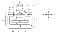
最初に、図1から図6を参照して、本発明の第1の実施の形態としての電流センサ1の構成について説明する。図1は、電流センサ1の全体構成例を表す斜視図である。図1に示したように、電流センサ1は、例えば磁気検出部2と、集磁コア3と、磁気シールド4とを有する。電流センサ1は、例えば導体5の近傍に配置される。導体5は、例えばZ軸方向に延在している。導体5には、Z軸方向に沿って、電流センサ1の検出対象である電流Imが流れるようになっている。図2Aは、電流センサ1の、Z軸方向と直交するXY面の断面を表す模式図である。図2Bは、電流センサ1のうち、磁気検出部2および磁気シールド4のYZ面の断面を拡大して表す模式図である。電流センサ1では、導体5に電流ImがZ軸方向に沿って+Zの向きに流れると、導体5の周囲には磁束Bmが誘導される。磁束Bmは、例えば集磁コア3の内部を通過する。磁束Bmは、磁気検出部2に対し、例えばX軸方向に沿った-Xの向きに印加されるようになっている。すなわち、磁気検出部2は、磁束Bmが-Xの向きに通過する位置に配置される。本実施の形態では、導体5の幅に沿った方向をX軸方向とし、導体5の厚さ方向をY軸方向とする。
本実施の形態の「Z軸方向」、「X軸方向」、および「Y軸方向」は、それぞれ、本発明の「第1方向」、「第2方向」、および「第3方向」に対応する一具体例である。
<1. First Embodiment>
[Configuration of current sensor 1]
First, the configuration of a current sensor 1 as a first embodiment of the present invention will be described with reference to FIGS. 1 to 6. FIG. FIG. 1 is a perspective view showing an example of the overall configuration of a current sensor 1. FIG. As shown in FIG. 1, the current sensor 1 has, for example, a magnetic detector 2, a magnetic collecting core 3, and a magnetic shield 4. As shown in FIG. The current sensor 1 is arranged near the conductor 5, for example. The conductor 5 extends, for example, in the Z-axis direction. A current Im to be detected by the current sensor 1 flows through the conductor 5 along the Z-axis direction. FIG. 2A is a schematic diagram showing a cross section of the current sensor 1 in the XY plane orthogonal to the Z-axis direction. FIG. 2B is a schematic diagram showing an enlarged cross-section of the magnetic detector 2 and the magnetic shield 4 in the YZ plane of the current sensor 1. FIG. In the current sensor 1 , when the current Im flows through the conductor 5 in the +Z direction along the Z-axis direction, a magnetic flux Bm is induced around the conductor 5 . The magnetic flux Bm passes through the magnetic collecting core 3, for example. The magnetic flux Bm is applied to the magnetic detector 2 in the -X direction along the X-axis direction, for example. That is, the magnetic detector 2 is arranged at a position through which the magnetic flux Bm passes in the -X direction. In this embodiment, the direction along the width of the conductor 5 is the X-axis direction, and the thickness direction of the conductor 5 is the Y-axis direction.
"Z-axis direction", "X-axis direction", and "Y-axis direction" of the present embodiment respectively correspond to "first direction", "second direction", and "third direction" of the present invention. It is one specific example to do.

(導体5)
導体5は、例えばCu(銅)などの高導電性非磁性材料により構成される。導体5は、例えばZ軸方向を長手方向とするように延在し、Y軸方向を厚み方向とする略板状体である。導体5は、おおよそ環状をなす集磁コア3により取り囲まれた空間を貫通するように配置されている。
(Conductor 5)
The conductor 5 is made of a highly conductive non-magnetic material such as Cu (copper). The conductor 5 is, for example, a substantially plate-like body extending in the Z-axis direction as the longitudinal direction and having the Y-axis direction as the thickness direction. The conductor 5 is arranged so as to pass through the space surrounded by the magnetism collecting core 3 which is approximately annular.

(集磁コア3)
集磁コア3は、自らを磁束Bmが通過するように磁束Bmを集束する軟磁性体である。図2Aに示したように、集磁コア3は、例えばZ軸方向と直交するXY面に沿って導体5を取り囲むように設けられている。なお、導体5を取り囲むとは、導体5の周囲を周回するように環状をなしている形態のみならず、導体5の周囲のうちの一部と対向する部分が欠落した状態の切り欠きを含む形態をも概念である。集磁コア3は、第1コア部31と、第2コア部32と、第3コア部33と、第4コア部34と、第5コア部35とを含んでいる。第1コア部31、第4コア部34、および第5コア部35は、いずれも、例えば導体5の幅方向であるX軸方向に延在している。第2コア部32および第3コア部33は、いずれも、例えば導体5の厚さ方向であるY軸方向に延在している。第1コア部31と、第4コア部34および第5コア部35とは、Y軸方向において対向するように配置されている。第2コア部32と第3コア部33とは、X軸方向において対向するように配置されている。第2コア部32は、第1コア部31のX軸方向の第1端部と、第4コア部34のX軸方向の第1端部とを繋ぐように設けられている。第4コア部34のX軸方向の第1端部と反対側の第2端部は、端面3T1を有している。第3コア部33は、第1コア部31のX軸方向の第1端部と反対側の第2端部と、第5コア部35のX軸方向の第1端部とを繋ぐように設けられている。第5コア部35のX軸方向の第1端部と反対側の第2端部は、端面3T2を有している。端面3T1と端面3T2とは、X軸方向に互いに離間して対向している。端面3T1と端面3T2とに挟まれた空間はコアギャップCGである。コアギャップCGは、X軸方向の幅W3を有する。なお、図2Aでは、第1コア部31と、第2コア部32と、第3コア部33と、第4コア部34と、第5コア部35とが互いに物理的に接触するように連結されている場合を例示しているが、本実施の形態はこれに限定されるものではない。例えば第1コア部31と、第2コア部32と、第3コア部33と、第4コア部34と、第5コア部35とが物理的に接触していなくとも、互いに磁気的に連結されていればよい。
(Magnetic collecting core 3)
The magnetic collecting core 3 is a soft magnetic material that collects the magnetic flux Bm so that the magnetic flux Bm passes through itself. As shown in FIG. 2A, the magnetism collecting core 3 is provided, for example, so as to surround the conductor 5 along the XY plane orthogonal to the Z-axis direction. It should be noted that "surrounding the conductor 5" includes not only the form of a ring formed around the conductor 5, but also a notch in which a part of the circumference of the conductor 5 facing a part is missing. Form is also a concept. The magnetic flux collecting core 3 includes a first core portion 31 , a second core portion 32 , a third core portion 33 , a fourth core portion 34 and a fifth core portion 35 . The first core portion 31, the fourth core portion 34, and the fifth core portion 35 all extend in the X-axis direction, which is the width direction of the conductor 5, for example. Both the second core portion 32 and the third core portion 33 extend in the Y-axis direction, which is the thickness direction of the conductor 5, for example. The first core portion 31, the fourth core portion 34, and the fifth core portion 35 are arranged to face each other in the Y-axis direction. The second core portion 32 and the third core portion 33 are arranged to face each other in the X-axis direction. The second core portion 32 is provided so as to connect the first end portion of the first core portion 31 in the X-axis direction and the first end portion of the fourth core portion 34 in the X-axis direction. A second end opposite to the first end in the X-axis direction of the fourth core portion 34 has an end face 3T1. The third core portion 33 connects the second end of the first core portion 31 opposite to the first end in the X-axis direction and the first end of the fifth core portion 35 in the X-axis direction. is provided. A second end opposite to the first end in the X-axis direction of the fifth core portion 35 has an end face 3T2. The end face 3T1 and the end face 3T2 face each other while being separated from each other in the X-axis direction. A space sandwiched between the end face 3T1 and the end face 3T2 is a core gap CG. The core gap CG has a width W3 in the X-axis direction. Note that in FIG. 2A, the first core portion 31, the second core portion 32, the third core portion 33, the fourth core portion 34, and the fifth core portion 35 are connected so as to physically contact each other. Although the case is exemplified, the present embodiment is not limited to this. For example, even if the first core portion 31, the second core portion 32, the third core portion 33, the fourth core portion 34, and the fifth core portion 35 are not in physical contact, they are magnetically connected to each other. It is good if it is.

図2Aに示した集磁コア3では、第1コア部31と第2コア部32との連結部、第1コア部31と第3コア部33との連結部、第2コア部32と第4コア部34との連結部、および第3コア部33と第5コア部35との連結部は、いずれも湾曲した形状を有している。しかしながら、本実施の形態はこの態様に限定されるものではない。例えば、これらの連結部は、屈曲した形状を有していてもよいし、角が面取りされた取り形状であってもよい。
本実施の形態の集磁コア3は、本発明の「第2軟磁性体」に対応する一具体例である。また、XY面は本発明の「第3平面」に対応する一具体例である。
In the magnetism collecting core 3 shown in FIG. 2A , the connecting portion between the first core portion 31 and the second core portion 32, the connecting portion between the first core portion 31 and the third core portion 33, the second core portion 32 and the third The connecting portion with the 4 core portion 34 and the connecting portion between the third core portion 33 and the fifth core portion 35 both have a curved shape. However, this embodiment is not limited to this aspect. For example, these connecting portions may have a bent shape or a chamfered shape.
The magnet collecting core 3 of the present embodiment is a specific example corresponding to the "second soft magnetic body" of the present invention. Also, the XY plane is a specific example corresponding to the "third plane" of the present invention.

(磁気検出部2)
磁気検出部2は、例えば端面3T1と端面3T2との隙間であるコアギャップCGに配置されている。電流センサ1では、導体5に電流Imが流れると導体5から磁束Bmが発生し、コアギャップCGを有する集磁コア3に磁束Bmが集束される。集磁コア3全体が磁束Bmの経路、すなわち磁路となる。したがって、コアギャップCGに設けられている磁気検出部2は、集磁コア3に集束される磁路に配置されることとなる。そのため、本実施形態において磁気検出部2がコアギャップCGに設けられる、とは、磁気検出部2の少なくとも一部が磁束Bmの経路に位置していればよいことを意味するものである。すなわち、磁気検出部2の全体がコアギャップCG内に位置していてもよいし、磁気検出部2の一部のみがコアギャップCG内に位置していてもよい。なお、磁気検出部2の詳細な構成については後述する。
(Magnetic detector 2)
The magnetic detection unit 2 is arranged, for example, in a core gap CG between the end surfaces 3T1 and 3T2. In the current sensor 1, when a current Im flows through the conductor 5, a magnetic flux Bm is generated from the conductor 5, and the magnetic flux Bm is focused on the magnetic flux collecting core 3 having the core gap CG. The magnetic flux collection core 3 as a whole forms a path of the magnetic flux Bm, that is, a magnetic path. Therefore, the magnetism detecting section 2 provided in the core gap CG is arranged in the magnetic path focused on the magnetic collecting core 3 . Therefore, in the present embodiment, the magnetic detection unit 2 is provided in the core gap CG means that at least part of the magnetic detection unit 2 should be positioned on the path of the magnetic flux Bm. That is, the entire magnetic detection section 2 may be positioned within the core gap CG, or only a portion of the magnetic detection section 2 may be positioned within the core gap CG. A detailed configuration of the magnetic detection unit 2 will be described later.

(磁気シールド4)
磁気シールド4は、外乱磁場から磁気検出部2を磁気的に遮蔽する部材である。すなわち、磁気シールド4は、検出対象とする磁束Bm以外の外部からの不要な磁場(磁束)の、磁気検出部2に対する影響を緩和する軟磁性体である。図2Bに示したように、磁気シールド4は、X軸方向と直交するYZ面に沿って磁気検出部2を取り囲むように、全体として環状の形状を有している。なお、磁気検出部2を取り囲むとは、磁気検出部2の周囲の周回するように環状をなしている形態のみならず、磁気検出部2の周囲のうちの一部と対向する部分が欠落した状態の切り欠きを含む形態をも概念である。磁気シールド4は、導体5および磁気検出部2の双方と物理的に接触することなく離間して配置されている。
(Magnetic shield 4)
The magnetic shield 4 is a member that magnetically shields the magnetic detector 2 from disturbance magnetic fields. In other words, the magnetic shield 4 is a soft magnetic material that mitigates the influence of an unnecessary external magnetic field (magnetic flux) other than the magnetic flux Bm to be detected on the magnetic detection section 2 . As shown in FIG. 2B, the magnetic shield 4 has an annular shape as a whole so as to surround the magnetic detection section 2 along the YZ plane perpendicular to the X-axis direction. It should be noted that the term “surrounding the magnetic detection unit 2” refers not only to the form of a circular shape that circulates around the magnetic detection unit 2, but also to the absence of a part of the circumference of the magnetic detection unit 2 that faces a part of the magnetic detection unit 2. It is also a concept to have a form that includes a state notch. The magnetic shield 4 is spaced apart from both the conductor 5 and the magnetic detection section 2 without physically contacting them.

磁気シールド4は、例えば第1シールド部41と、第2シールド部42と、第3シールド部43と、第4シールド部44とを含んでいる。第1シールド部41および第2シールド部42は、Z軸方向およびX軸方向を含むXZ面に沿って広がっている。第3シールド部43および第4シールド部44は、例えば導体5の厚さ方向であるY軸方向に延在している。第1シールド部41と第2シールド部42とは、Y軸方向において対向するように配置されている。第1シールド部41は、Y軸方向において例えばコアギャップCGから見て導体5の反対側に位置する。第2シールド部42は、導体5と第1シールド部41との間に配置される。第2シールド部42は、Y軸方向において、例えばコアギャップCGと導体5との間に位置する。また、磁気検出部2は、XZ面に直交するY軸方向に眺めた状態で第1シールド部41および第2シールド部42の双方と重なり合うように配置されている。第3シールド部43と第4シールド部44とは、Z軸方向において対向するように配置されている。第3シールド部43は、第1シールド部41のZ軸方向の第1端部411と、第2シールド部42のZ軸方向の第1端部421とを磁気的に繋ぐように設けられている。第4シールド部44は、第1シールド部41のZ軸方向の第1端部411と反対側の第2端部412と、第2シールド部42のZ軸方向の第1端部421と反対側の第2端部422とを磁気的に繋ぐように設けられている。なお、図2Bでは、第1シールド部41と、第2シールド部42と、第3シールド部43と、第4シールド部44とが互いに物理的に接触するように連結されている場合を例示しているが、本実施の形態はこれに限定されるものではない。例えば第1シールド部41と、第2シールド部42と、第3シールド部43と、第4シールド部44とが物理的に接触していなくとも、互いに磁気的に連結されている状態であればよい。ここでいう磁気的に連結されている状態とは、例えば0.05mm以下の間隔となるように近接して配置されている状態をいう。互いに連結される2つのシールド部同士の間隔が例えば0.1mm以上であると、磁気的に分割され、磁気的なシールド効果が低減してしまう。 The magnetic shield 4 includes a first shield portion 41, a second shield portion 42, a third shield portion 43, and a fourth shield portion 44, for example. The first shield part 41 and the second shield part 42 spread along the XZ plane including the Z-axis direction and the X-axis direction. The third shield part 43 and the fourth shield part 44 extend in the Y-axis direction, which is the thickness direction of the conductor 5, for example. The first shield part 41 and the second shield part 42 are arranged so as to face each other in the Y-axis direction. The first shield part 41 is located on the opposite side of the conductor 5 from the core gap CG in the Y-axis direction, for example. The second shield part 42 is arranged between the conductor 5 and the first shield part 41 . The second shield part 42 is positioned, for example, between the core gap CG and the conductor 5 in the Y-axis direction. The magnetic detection section 2 is arranged so as to overlap both the first shield section 41 and the second shield section 42 when viewed in the Y-axis direction perpendicular to the XZ plane. The third shield part 43 and the fourth shield part 44 are arranged so as to face each other in the Z-axis direction. The third shield portion 43 is provided so as to magnetically connect the first end portion 411 of the first shield portion 41 in the Z-axis direction and the first end portion 421 of the second shield portion 42 in the Z-axis direction. there is The fourth shield part 44 has a second end 412 opposite to the first end 411 in the Z-axis direction of the first shield part 41 and a first end 421 in the Z-axis direction of the second shield part 42 . It is provided so as to be magnetically connected to the second end 422 on the side. Note that FIG. 2B illustrates a case where the first shield part 41, the second shield part 42, the third shield part 43, and the fourth shield part 44 are connected so as to physically contact each other. However, the present embodiment is not limited to this. For example, even if the first shield part 41, the second shield part 42, the third shield part 43, and the fourth shield part 44 are not in physical contact, if they are magnetically connected to each other, good. The state of being magnetically coupled here means the state of being arranged close to each other with an interval of 0.05 mm or less, for example. If the distance between the two shield portions that are connected to each other is, for example, 0.1 mm or more, they will be magnetically divided and the magnetic shielding effect will be reduced.

図2Bの例では、第1シールド部41のX軸方向の寸法である幅W41と第2シールド部42のX軸方向の寸法である幅W42とは、互いに実質的に等しい。また、幅W41および幅W42は、例えば集磁コア3のコアギャップCGの幅W3よりも狭い(W41,W42<W3)。なお、幅W41,W42は例えば2mm以上10mm以下とし、幅W3は例えば4mm以上12mm以下とすることができる。 In the example of FIG. 2B, the width W41, which is the dimension of the first shield part 41 in the X-axis direction, and the width W42, which is the dimension of the second shield part 42 in the X-axis direction, are substantially equal to each other. Also, the width W41 and the width W42 are narrower than the width W3 of the core gap CG of the magnet collecting core 3 (W41, W42<W3). The widths W41 and W42 can be, for example, 2 mm or more and 10 mm or less, and the width W3 can be, for example, 4 mm or more and 12 mm or less.

図2Bに示した磁気シールド4では、第1シールド部41と第3シールド部43との連結部、第3シールド部43と第2シールド部42との連結部、第2シールド部42と第4シールド部44との連結部、第4シールド部44と第1シールド部41との連結部は、いずれも湾曲した形状を有している。しかしながら、本実施の形態はこの態様に限定されるものではない。例えば、これらの連結部は、屈曲した形状を有していてもよいし、角が面取りされた取り形状であってもよい。
本実施の形態の磁気シールド4は、本発明の「第1軟磁性体」に対応する一具体例である。また、本実施の形態のYZ面は、本発明の「第1平面」に対応する一具体例である。さらに、本実施の形態のXZ面は、本発明の「第2平面」に対応する一具体例である。
In the magnetic shield 4 shown in FIG. 2B, the connecting portion between the first shield portion 41 and the third shield portion 43, the connecting portion between the third shield portion 43 and the second shield portion 42, the second shield portion 42 and the fourth shield portion The connecting portion with the shield portion 44 and the connecting portion between the fourth shield portion 44 and the first shield portion 41 both have a curved shape. However, this embodiment is not limited to this aspect. For example, these connecting portions may have a bent shape or a chamfered shape.
The magnetic shield 4 of this embodiment is a specific example corresponding to the "first soft magnetic body" of the present invention. Also, the YZ plane of the present embodiment is a specific example corresponding to the "first plane" of the invention. Furthermore, the XZ plane of this embodiment is a specific example corresponding to the "second plane" of the present invention.

集磁コア3および磁気シールド4は、例えば、珪素鋼、電磁鋼、純鉄(SUY)、パーマロイ等の軟磁性材料を主たる構成材料として含んでいる。集磁コア3は、磁気シールド4と比べて磁束Bmの印加により着磁されやすいので、比較的残留磁化が小さい材料であるFeSiやパーマロイにより構成されるとよい。一方、磁気シールド4は集磁コア3と比べて磁束Bmによる着磁がなされにくいので、比較的残留磁化が大きい材料である純鉄Fなどを用いることができる。 The magnetic collecting core 3 and the magnetic shield 4 contain, for example, soft magnetic materials such as silicon steel, electromagnetic steel, pure iron (SUY), and permalloy as main constituent materials. The magnetic collecting core 3 is more likely to be magnetized by application of the magnetic flux Bm than the magnetic shield 4, so it is preferably made of FeSi or permalloy, which is a material with relatively small residual magnetization. On the other hand, since the magnetic shield 4 is less likely to be magnetized by the magnetic flux Bm than the magnetic collecting core 3, pure iron F or the like, which is a material with relatively large residual magnetization, can be used.

また、磁気シールド4の構成材料の鉄損は、例えば集磁コア3の構成材料の鉄損よりも大きいことが望ましい。導体5に所定の電流Imが流れることにより導体5から発生する磁束Bmは集磁コア3および磁気シールド4に流れる。導体5に流れる電流Imの周波数が高くなると、鉄損が相対的に大きい材料により構成される磁気シールド4の周波数特性が低下し、磁気シールド4に流れる磁束Bmが相対的に減少する。電流Imの周波数が高くなると、鉄損が相対的に小さい材料により構成される集磁コア3においても周波数特性が低下し、磁束Bmが流れにくくなるものの、磁気シールド4に流れる磁束Bmが相対的に減少する分、集磁コア3に流れる磁束Bmが相対的に増加する。その結果として、磁気シールド4を有しない電流センサ1に比べ、磁気検出部2に印加される磁束Bmの磁束密度は安定すると考えられる。磁気シールド4の構成材料の鉄損と集磁コア3の構成材料の鉄損の差が大きくなるほど、周波数特性が改善され、磁気検出部2に印加される磁束Bmの磁束密度の減衰を抑制することができる。その結果、交流電流に対する電流センサ1の応答特性を安定化させることができる。集磁コア3の構成材料の鉄損と磁気シールド4の構成材料の鉄損との差は、例えば、2.0W/kg以上であることが好ましく、4.5W/kg以上10.0W/kg以下であることがより好ましい。鉄損は、JIS-C-2550の規定に基づくエプスタイン試験法に従い、周波数50Hz時の最大磁束密度1.5Tの正弦波励磁のときの単位重量当たりの鉄損の大きさ(圧延方向とそれに対する直角方向の平均)として求められる値である。なお、集磁コア3の構成材料は、磁気シールド4の構成材料と同一種類の材料であってもよいし、異なる種類の材料であってもよい。例えば、集磁コア3と磁気シールド4とがともに電磁鋼により構成されるが、磁気シールド4を構成する電磁鋼の鉄損が、集磁コア3を構成する電磁鋼の鉄損よりも大きいとよい。 In addition, it is desirable that the core loss of the constituent material of the magnetic shield 4 is larger than the core loss of the constituent material of the magnetic collecting core 3, for example. A magnetic flux Bm generated from the conductor 5 flows through the magnetic collecting core 3 and the magnetic shield 4 when a predetermined current Im flows through the conductor 5 . As the frequency of the current Im flowing through the conductor 5 increases, the frequency characteristic of the magnetic shield 4 made of a material with relatively large iron loss deteriorates, and the magnetic flux Bm flowing through the magnetic shield 4 relatively decreases. When the frequency of the current Im increases, the frequency characteristics of the magnetic flux collecting core 3 made of a material with relatively small iron loss also deteriorate, and although the magnetic flux Bm becomes difficult to flow, the magnetic flux Bm flowing through the magnetic shield 4 is relatively low. , the magnetic flux Bm flowing through the magnetic collecting core 3 relatively increases. As a result, it is considered that the magnetic flux density of the magnetic flux Bm applied to the magnetic detection section 2 is stable compared to the current sensor 1 without the magnetic shield 4 . As the difference between the iron loss of the material forming the magnetic shield 4 and the iron loss of the material forming the magnetic core 3 increases, the frequency characteristics are improved, and the attenuation of the magnetic flux density of the magnetic flux Bm applied to the magnetic detection unit 2 is suppressed. be able to. As a result, it is possible to stabilize the response characteristics of the current sensor 1 with respect to alternating current. The difference between the iron loss of the material forming the magnetic collecting core 3 and the iron loss of the material forming the magnetic shield 4 is preferably, for example, 2.0 W/kg or more, 4.5 W/kg or more, and 10.0 W/kg. The following are more preferable. The iron loss is determined according to the Epstein test method based on JIS-C-2550, and the magnitude of iron loss per unit weight (rolling direction and is the value obtained as the average of the perpendicular directions). The material of the magnetic collecting core 3 may be the same type of material as the material of the magnetic shield 4, or may be of a different type. For example, both the magnetic core 3 and the magnetic shield 4 are made of electromagnetic steel. good.

図3は、電流センサの概略構成を示すブロック図である。図3に示したように、電流センサ1は、磁気検出部2と信号処理部60とを備える。信号処理部60は、例えばA/D(アナログ-デジタル)変換部61と、演算部62とを含む。A/D変換部61は、磁気検出部2から出力されるアナログ信号をデジタル信号に変換する。演算部62は、A/D変換部61によりデジタル変換されたデジタル信号を演算処理する。なお、信号処理部60は、演算部62の下流側にD/A(デジタル-アナログ)変換部をさらに含んでいてもよい。D/A変換部を含むことにより、信号処理部60は、演算部62にて演算処理された演算処理結果をアナログ信号として出力することができる。 FIG. 3 is a block diagram showing a schematic configuration of the current sensor. As shown in FIG. 3 , the current sensor 1 has a magnetic detection section 2 and a signal processing section 60 . The signal processing unit 60 includes an A/D (analog-digital) conversion unit 61 and a calculation unit 62, for example. The A/D converter 61 converts the analog signal output from the magnetic detector 2 into a digital signal. The calculation unit 62 performs calculation processing on the digital signal converted by the A/D conversion unit 61 . Note that the signal processing section 60 may further include a D/A (digital-analog) conversion section on the downstream side of the calculation section 62 . By including the D/A conversion section, the signal processing section 60 can output the result of arithmetic processing performed by the arithmetic section 62 as an analog signal.

図4は、図1に示した磁気検出部2の回路構成を概略的に表す回路図である。図4に示したように、磁気検出部2は、例えば第1抵抗部R1、第2抵抗部R2、第3抵抗部R3、および第4抵抗部R4の4つの抵抗部をブリッジ接続してなるホイートストンブリッジ回路Cを有する。但し、磁気検出部2は、第1抵抗部R1および第2抵抗部R2の2つの抵抗部をハーフブリッジ接続してなる回路を有するものであってもよい。第1~第4抵抗部R1~R4は、それぞれ一の磁気抵抗効果素子(MR素子)又は一のホール素子を含んでいてもよいし、複数の磁気抵抗効果素子又は複数のホール素子を含んでいてもよい。磁気抵抗効果素子は、例えばAMR素子、GMR素子、またはTMR素子などである。 FIG. 4 is a circuit diagram schematically showing the circuit configuration of the magnetic detection section 2 shown in FIG. As shown in FIG. 4, the magnetic detection section 2 is formed by bridge-connecting four resistance sections, for example, a first resistance section R1, a second resistance section R2, a third resistance section R3, and a fourth resistance section R4. It has a Wheatstone bridge circuit C. However, the magnetic detection section 2 may have a circuit formed by half-bridge connecting two resistance sections, the first resistance section R1 and the second resistance section R2. Each of the first to fourth resistance units R1 to R4 may include one magnetoresistive effect element (MR element) or one Hall element, or may include a plurality of magnetoresistive effect elements or a plurality of Hall elements. You can The magnetoresistive element is, for example, an AMR element, a GMR element, or a TMR element.

磁気検出部2が有するホイートストンブリッジ回路Cは、電源ポートVと、グランドポートGと、2つの出力ポートE1,E2と、直列に接続された第1抵抗部R1および第2抵抗部R2と、直列に接続された第3抵抗部R3および第4抵抗部R4とを含む。第1抵抗部R1および第3抵抗部R3の各一端は、電源ポートVに接続される。第1抵抗部R1の他端は、第2抵抗部R2の一端と出力ポートE1とに接続される。第3抵抗部R3の他端は、第4抵抗部R4の一端と出力ポートE2とに接続される。第2抵抗部R2および第4抵抗部R4の各他端は、グランドポートGに接続される。電源ポートVには、所定の大きさの電源電圧が印加され、グランドポートGはグランドに接続される。 The Wheatstone bridge circuit C included in the magnetic detection unit 2 includes a power supply port V, a ground port G, two output ports E1 and E2, and a first resistance unit R1 and a second resistance unit R2 connected in series. and a third resistor portion R3 and a fourth resistor portion R4 connected to . One end of each of the first resistor portion R1 and the third resistor portion R3 is connected to the power port V. As shown in FIG. The other end of the first resistance portion R1 is connected to one end of the second resistance portion R2 and the output port E1. The other end of the third resistor R3 is connected to one end of the fourth resistor R4 and the output port E2. Each other end of the second resistance portion R2 and the fourth resistance portion R4 is connected to the ground port G. A power supply voltage of a predetermined magnitude is applied to the power supply port V, and the ground port G is connected to the ground.

図5は、図4に示した第1~第4抵抗部R1~R4を構成するGMR素子又はTMR素子等のMR素子の概略構成例を表す示す斜視図である。第1~第4抵抗部R1~R4を構成するMR素子は、例えば図5に示したように、複数の第1電極71と、複数のMR膜80と、複数の第2電極72とを有している。複数の第1電極71は、例えば基板上に設けられている。第1電極71は、下部リード電極とも称される。各第1電極71は細長い形状を有する。第1電極71の長手方向に隣接する2つの第1電極71の間には、間隙が形成されている。第1電極71の上面における、長手方向の両端近傍にそれぞれMR膜80が設けられている。図6は、図5に示した第1~第4抵抗部R1~R4を構成するMR素子の断面構成例を表す概略断面図である。図6に示したように、MR膜80は、平面視略円形状であり、第1電極71側から順に積層された自由層81、非磁性層82、磁化固定層83及び反強磁性層84を含む。自由層81は、第1電極71に電気的に接続されている。反強磁性層84は、反強磁性材料により構成され、磁化固定層83との間で交換結合を生じさせることで、磁化固定層83の磁化の方向を固定する役割を果たす。複数の第2電極72は、複数のMR膜80上に設けられている。各第2電極72は細長い形状を有し、第1電極71の長手方向に隣接する2つの第1電極71上に配置され、隣接する2つのMR膜80の反強磁性層84同士を電気的に接続する。第2電極72は、上部リード電極とも称される。なお、MR膜80は、第2電極72に近い位置から順に自由層81、非磁性層82、磁化固定層83および反強磁性層84が積層されてなる構成を有していてもよい。また、磁化固定層83を、強磁性層/非磁性中間層/強磁性層の積層フェリ構造とし、両強磁性層を反強磁性的に結合させてなる、いわゆるセルフピン止め型の固定層(Synthetic Ferri Pinned層,SFP層)とすることで、反強磁性層84が省略されていてもよい。 FIG. 5 is a perspective view showing a schematic configuration example of an MR element such as a GMR element or a TMR element forming the first to fourth resistance parts R1 to R4 shown in FIG. The MR elements constituting the first to fourth resistance parts R1 to R4 have a plurality of first electrodes 71, a plurality of MR films 80, and a plurality of second electrodes 72, as shown in FIG. are doing. The multiple first electrodes 71 are provided, for example, on a substrate. The first electrode 71 is also called a lower lead electrode. Each first electrode 71 has an elongated shape. A gap is formed between two first electrodes 71 adjacent to each other in the longitudinal direction. MR films 80 are provided near both longitudinal ends of the upper surface of the first electrode 71 . FIG. 6 is a schematic cross-sectional view showing a cross-sectional configuration example of the MR element that constitutes the first to fourth resistance parts R1 to R4 shown in FIG. As shown in FIG. 6, the MR film 80 has a substantially circular shape in plan view, and includes a free layer 81, a nonmagnetic layer 82, a magnetization fixed layer 83, and an antiferromagnetic layer 84 which are stacked in order from the first electrode 71 side. including. The free layer 81 is electrically connected to the first electrode 71 . The antiferromagnetic layer 84 is made of an antiferromagnetic material and serves to fix the magnetization direction of the magnetization fixed layer 83 by causing exchange coupling with the magnetization fixed layer 83 . The multiple second electrodes 72 are provided on the multiple MR films 80 . Each second electrode 72 has an elongated shape, is arranged on two first electrodes 71 adjacent in the longitudinal direction of the first electrode 71, and electrically connects the antiferromagnetic layers 84 of the two adjacent MR films 80 together. connect to. The second electrode 72 is also called an upper lead electrode. Note that the MR film 80 may have a structure in which a free layer 81 , a nonmagnetic layer 82 , a magnetization fixed layer 83 and an antiferromagnetic layer 84 are stacked in this order from the position closest to the second electrode 72 . The magnetization fixed layer 83 has a laminated ferrimagnetic structure of ferromagnetic layer/nonmagnetic intermediate layer/ferromagnetic layer, and the two ferromagnetic layers are antiferromagnetically coupled to form a so-called self-pinned fixed layer (synthetic layer). (Ferri Pinned layer, SFP layer), the antiferromagnetic layer 84 may be omitted.

TMR素子においては、非磁性層82はトンネルバリア層である。GMR素子においては、非磁性層82は非磁性導電層である。TMR素子およびGMR素子において、自由層81の磁化の方向が磁化固定層83の磁化の方向に対してなす角度に応じて抵抗値が変化し、この角度が0°(互いの磁化方向が平行)のときに抵抗値が最小となり、180°(互いの磁化方向が反平行)のときに抵抗値が最大となる。 In the TMR element, the nonmagnetic layer 82 is a tunnel barrier layer. In the GMR element, the nonmagnetic layer 82 is a nonmagnetic conductive layer. In the TMR element and the GMR element, the resistance value changes according to the angle formed by the magnetization direction of the free layer 81 with respect to the magnetization direction of the magnetization fixed layer 83, and this angle is 0° (the magnetization directions are parallel to each other). The resistance value is minimum when , and the resistance value is maximum when 180° (the magnetization directions are antiparallel to each other).

第1~第4抵抗部R1~R4がTMR素子またはGMR素子により構成される場合、磁気検出部2のホイートストンブリッジ回路Cにおいて、第1抵抗部R1および第2抵抗部R2の磁化固定層83の磁化方向はX方向に平行であって、第1抵抗部R1の磁化固定層83の磁化方向と、第2抵抗部R2の磁化固定層83の磁化方向とは、互いに反平行方向である。また、第3抵抗部R3及び第4抵抗部R4の磁化固定層83の磁化方向はX方向に平行であって、第3抵抗部R3の磁化固定層83の磁化方向と、第4抵抗部R4の磁化固定層83の磁化方向とは、互いに反平行方向である。磁気検出部2において、導体5から発生するX方向の磁場の磁界強度の変化に応じて、出力ポートE1,E2の電位差が変化し、出力ポートE1,E2の電位差に対応する信号がセンサ信号Sとして信号処理部60に出力される。差分検出器により、出力ポートE1,E2の電位差に対応する信号を増幅し、センサ信号Sとして信号処理部60のA/D変換部61に出力するとよい。 When the first to fourth resistance sections R1 to R4 are configured by TMR elements or GMR elements, in the Wheatstone bridge circuit C of the magnetic detection section 2, the magnetization fixed layers 83 of the first resistance section R1 and the second resistance section R2 are The magnetization direction is parallel to the X direction, and the magnetization direction of the magnetization pinned layer 83 of the first resistance portion R1 and the magnetization direction of the magnetization pinned layer 83 of the second resistance portion R2 are antiparallel to each other. The magnetization directions of the magnetization pinned layers 83 of the third resistor portion R3 and the fourth resistor portion R4 are parallel to the X direction, and the magnetization directions of the magnetization pinned layers 83 of the third resistor portion R3 and the magnetization directions of the magnetization pinned layers 83 of the fourth resistor portion R4 are parallel to each other. are antiparallel to each other. In the magnetic detection unit 2, the potential difference between the output ports E1 and E2 changes according to changes in the magnetic field strength of the magnetic field in the X direction generated from the conductor 5, and the signal corresponding to the potential difference between the output ports E1 and E2 is the sensor signal S is output to the signal processing unit 60 as. A signal corresponding to the potential difference between the output ports E1 and E2 may be amplified by a difference detector and output as the sensor signal S to the A/D converter 61 of the signal processor 60 .

A/D変換部61は、磁気検出部2から出力されるセンサ信号S(電流に関するアナログ信号)をデジタル信号に変換し、当該デジタル信号が演算部62に入力される。演算部62は、A/D変換部61によりアナログ信号から変換されたデジタル信号についての演算処理を行う。この演算部62は、例えば、マイクロコンピュータ、ASIC(Application Specific Integrated Circuit)などにより構成される。 The A/D conversion section 61 converts the sensor signal S (analog signal related to current) output from the magnetic detection section 2 into a digital signal, and the digital signal is input to the calculation section 62 . The calculation unit 62 performs calculation processing on the digital signal converted from the analog signal by the A/D conversion unit 61 . The calculation unit 62 is configured by, for example, a microcomputer, an ASIC (Application Specific Integrated Circuit), or the like.

[電流センサ1の作用効果]
本実施形態の電流センサ1によれば、集磁コア3のコアギャップCGに配置された磁気検出部2を取り囲むように磁気シールド4を設けるようにしている。このため、磁気検出部2に対する、周囲からの不要な外乱磁場の磁束の影響が緩和される。例えば外乱磁場のうちの、Y軸方向に沿った磁場成分HyおよびZ軸方向に沿った磁場成分Hzは、例えば図7に示したように、主に磁気シールド4を通過する。このため、磁気シールド4に取り囲まれた空間に配置されている磁気検出部2を通過する磁場成分Hyおよび磁場成分Hzは低減される。なお、図7は、電流センサ1の作用効果を説明するための第1の説明図である。例えば磁場成分Hzは2つに分流し、Y軸方向において互いに対向するように配置されてXZ面に沿って広がる第1シールド部41および第2シールド部42をそれぞれ通過することとなる。また、磁場成分Hyも2つに2つに分流し、Z軸方向において互いに対向するように配置されてXY面に沿って広がる第3シールド部43および第4シールド部44をそれぞれ通過することとなる。図7では、磁場成分Hzの経路を実線矢印で模式的に表し、磁場成分Hyの経路を破線矢印で模式的に表している。
[Action and effect of current sensor 1]
According to the current sensor 1 of this embodiment, the magnetic shield 4 is provided so as to surround the magnetic detector 2 arranged in the core gap CG of the magnetic core 3 . Therefore, the influence of the magnetic flux of the unwanted disturbance magnetic field from the surroundings on the magnetic detection section 2 is alleviated. For example, of the disturbance magnetic field, the magnetic field component Hy along the Y-axis direction and the magnetic field component Hz along the Z-axis direction mainly pass through the magnetic shield 4 as shown in FIG. Therefore, the magnetic field component Hy and the magnetic field component Hz passing through the magnetic detection section 2 arranged in the space surrounded by the magnetic shield 4 are reduced. 7A and 7B are first explanatory diagrams for explaining the effects of the current sensor 1. FIG. For example, the magnetic field component Hz is split into two and passes through the first shield part 41 and the second shield part 42 that are arranged to face each other in the Y-axis direction and spread along the XZ plane. In addition, the magnetic field component Hy is also split into two and passes through the third shield part 43 and the fourth shield part 44 that are arranged to face each other in the Z-axis direction and spread along the XY plane. Become. In FIG. 7, the path of the magnetic field component Hz is schematically represented by solid arrows, and the path of the magnetic field component Hy is schematically represented by broken arrows.

ところが、図8に示した参考例としての電流センサ101のように、例えば磁気シールド4を有しない場合、磁場成分Hyは集磁コア3を通過したのち磁気検出部2に集中して向かうこととなってしまう。なお、電流センサ101の構成は、磁気シールド4を有しないことを除き、電流センサ1と実質的に同じ構成である。 However, in the case where the current sensor 101 as a reference example shown in FIG. turn into. The configuration of the current sensor 101 is substantially the same as that of the current sensor 1 except that the magnetic shield 4 is not provided.

これに対し、本実施の形態の電流センサ1では、例えば図9に示したように、集磁コア3に流入して端面3T1,3T2から流出した磁場成分Hyは、分岐して第1シールド部41および第2シールド部42に流入する。その結果、+Y方向の磁場成分Hyと-Y方向の磁場成分Hyとが相殺され、磁場成分Hyが実質的に存在しない領域Rが発生する。そこで磁気検出部2の第1~第4抵抗部R1~R4を領域Rに配置することで、磁気検出部2に対する磁場成分Hyの影響を低減することができる。なお、図9は、電流センサ1の作用効果を説明するための第2の説明図である。 On the other hand, in the current sensor 1 of the present embodiment, as shown in FIG. 9 for example, the magnetic field component Hy flowing into the magnetic collecting core 3 and flowing out from the end surfaces 3T1 and 3T2 is branched to the first shield portion 41 and the second shield part 42 . As a result, the magnetic field component Hy in the +Y direction and the magnetic field component Hy in the −Y direction are offset, and a region R in which the magnetic field component Hy does not substantially exist is generated. Therefore, by arranging the first to fourth resistors R1 to R4 of the magnetic detection section 2 in the region R, the influence of the magnetic field component Hy on the magnetic detection section 2 can be reduced. 9A and 9B are second explanatory diagrams for explaining the effects of the current sensor 1. FIG.

また、電流センサ1では、外乱磁場のうちの、X軸方向に沿った磁場成分Hxについても磁気検出部2に到達するのを抑制することができる。図10に示したように、磁場成分Hxは、分岐して磁気シールド4のうちの第1シールド部41および第2シールド部42の幅方向の第1端部にそれぞれ流入し、反対側の幅方向の第2端部から流出するからである。なお、図10は、電流センサ1の作用効果を説明するための第3の説明図である。 Further, in the current sensor 1 , it is possible to suppress the magnetic field component Hx along the X-axis direction of the disturbance magnetic field from reaching the magnetic detection section 2 . As shown in FIG. 10, the magnetic field component Hx branches off and flows into the first widthwise first ends of the first shield portion 41 and the second shield portion 42 of the magnetic shield 4, and the width direction of the opposite side. This is because it flows out from the second end of the direction. Note that FIG. 10 is a third explanatory diagram for explaining the effects of the current sensor 1. As shown in FIG.

また、電流センサ1および電流センサ101では、導体5に流れる電流Imが大きくなると、集磁コア3が磁気的に飽和しやすくなる。そのため、磁気検出部2の出力の線形性が劣化し、検出される電流値の測定精度に支障を来す可能性がある。それを避けるために、軟磁性体である集磁コア3の体積を増加させることもできるが、電流センサ1および電流センサ101の寸法の増大を招くので望ましくない。そこで、集磁コア3の磁気的な飽和を避ける他の手法として、コアギャップCGの幅W3を拡大するなどして磁気回路の磁気抵抗を増大させることが考えられる。しかしながら、その場合、電流センサ101のように磁気シールド4を有しない構造では、磁気検出部2が外乱磁場の影響を受けやすくなってしまう。その点、本実施の形態の電流センサ1では、磁気シールド4をコアギャップCGに配置するようにしている。このため、コアギャップCGの幅W3を拡大して磁気回路の磁気抵抗を増大させることで集磁コア3の磁気的な飽和を避けつつ、磁気検出部2に及ぶ外乱磁場の影響を緩和することができる。 Further, in the current sensor 1 and the current sensor 101, when the current Im flowing through the conductor 5 increases, the magnetism collecting core 3 tends to be magnetically saturated. As a result, the linearity of the output of the magnetic detection unit 2 is degraded, which may interfere with the measurement accuracy of the detected current value. In order to avoid this, it is possible to increase the volume of the magnetic flux collection core 3 which is a soft magnetic material, but this is undesirable because it causes an increase in the dimensions of the current sensors 1 and 101 . Therefore, as another method for avoiding the magnetic saturation of the magnet collecting core 3, it is conceivable to increase the magnetic resistance of the magnetic circuit by enlarging the width W3 of the core gap CG. However, in that case, in a structure without the magnetic shield 4 like the current sensor 101, the magnetic detection section 2 is likely to be affected by the disturbance magnetic field. In this regard, in the current sensor 1 of the present embodiment, the magnetic shield 4 is arranged in the core gap CG. Therefore, the width W3 of the core gap CG is increased to increase the magnetic resistance of the magnetic circuit, thereby avoiding the magnetic saturation of the magnetic collecting core 3 and mitigating the influence of the disturbance magnetic field on the magnetic detection unit 2. can be done.

さらに、本実施の形態の電流センサ1では、集磁コア3の残留磁化および磁気シールド4の残留磁化の影響の低減効果も得られる。軟磁性体である集磁コア3および磁気シールド4は、図11に示したように、それぞれ、磁束Bmの付与により残留磁化を生ずる。具体的には、集磁コア3では、例えば第1コア部31には-X方向の残留磁化3Mrが生じ、第4コア部34および第5コア部35には+X方向の残留磁化3Mrが生じる。その結果、コアギャップCGでは+X方向の残留磁束3Brが発生する。また、磁気シールド4では、例えば第1シールド部41には+X方向の残留磁化41Mrが生じ、第2シールド部42には+X方向の残留磁化42Mrが生じる。その結果、コアギャップCGでは、第1シールド部41の周囲に残留磁束41Brが発生すると共に第2シールド部42の周囲に残留磁束42Brが発生する。残留磁束41Brおよび残留磁束42Brは、磁気検出部2に対しては-X方向に付与される。したがって、磁気検出部2の近傍では、+X方向の残留磁束3Brと-X方向の残留磁束41Br,42Brとが相殺しあうこととなり、実質的に磁気検出部2に付与される残留磁束は十分に低減される。よって、磁気検出部2は、集磁コア3の残留磁化3Mrおよび磁気シールド4の残留磁化41Mr,42Mrの影響を実質的に受けることなく、測定対象とする磁束Bmを高い精度で検出することができる。集磁コア3の残留磁束3Brと、および磁気シールド4の残留磁束41Br,42Brとが相殺される領域は1か所、または2か所形成することができる。第1シールド部41の材質および寸法ならびに第2シールド部42の材質および寸法を適宜選択すればよい。なお、図11は、電流センサ1の作用効果を説明するための第4の説明図である。 Furthermore, in the current sensor 1 of the present embodiment, the effect of reducing the influence of the residual magnetization of the magnet collecting core 3 and the residual magnetization of the magnetic shield 4 can also be obtained. As shown in FIG. 11, the magnetic flux collection core 3 and the magnetic shield 4, which are soft magnetic bodies, each generate residual magnetization when magnetic flux Bm is applied. Specifically, in the magnetic flux collecting core 3, for example, a residual magnetization 3Mr in the −X direction is generated in the first core portion 31, and a residual magnetization 3Mr in the +X direction is generated in the fourth core portion 34 and the fifth core portion 35. . As a result, a residual magnetic flux 3Br in the +X direction is generated in the core gap CG. Further, in the magnetic shield 4, for example, the first shield portion 41 has residual magnetization 41Mr in the +X direction, and the second shield portion 42 has residual magnetization 42Mr in the +X direction. As a result, a residual magnetic flux 41Br is generated around the first shield portion 41 and a residual magnetic flux 42Br is generated around the second shield portion 42 in the core gap CG. The residual magnetic flux 41Br and the residual magnetic flux 42Br are applied to the magnetic detection section 2 in the -X direction. Therefore, in the vicinity of the magnetic detection section 2, the residual magnetic flux 3Br in the +X direction and the residual magnetic fluxes 41Br and 42Br in the -X direction cancel each other out, and substantially the residual magnetic flux applied to the magnetic detection section 2 is sufficient. reduced. Therefore, the magnetic detector 2 can detect the magnetic flux Bm to be measured with high accuracy without being substantially affected by the residual magnetization 3Mr of the magnet collecting core 3 and the residual magnetizations 41Mr and 42Mr of the magnetic shield 4. can. One or two regions can be formed in which the residual magnetic flux 3Br of the magnetic collecting core 3 and the residual magnetic fluxes 41Br and 42Br of the magnetic shield 4 are offset. The material and dimensions of the first shield part 41 and the material and dimensions of the second shield part 42 may be selected as appropriate. 11A and 11B are fourth explanatory diagrams for explaining the effects of the current sensor 1. FIG.

このように、本実施の形態の電流センサ1によれば、検出対象とする磁束Bmを磁気検出部2に到達させつつ、磁気検出部2に対する、周囲からの不要な外乱磁場の磁束の影響を緩和することができる。よって、磁束Bmを高い精度で検出し、導体5を流れる電流Imの大きさを高い精度で測定することができる。 As described above, according to the current sensor 1 of the present embodiment, while allowing the magnetic flux Bm to be detected to reach the magnetic detection unit 2, the influence of the magnetic flux of the unnecessary disturbance magnetic field from the surroundings on the magnetic detection unit 2 is suppressed. can be mitigated. Therefore, the magnetic flux Bm can be detected with high accuracy, and the magnitude of the current Im flowing through the conductor 5 can be measured with high accuracy.

[第1の実施の形態の変形例]
(変形例1-1)
図12は、上記第1の実施の形態の第1変形例(変形例1-1)としての電流センサ1Aを表す断面模式図である。上記第1の実施の形態の電流センサ1では、例えば図2Aに示したように、磁気シールド4の第1シールド部41の幅W41および第2シールド部42の幅W42が、集磁コア3のコアギャップCGの幅W3よりも狭くなるようにした(W41,W42<W3)。これに対し、変形例1-1としての電流センサ1Aでは、図12に示したように、磁気シールド4の第1シールド部41の幅W41および第2シールド部42の幅W42が、集磁コア3のコアギャップCGの幅W3よりも広くなるようにしている(W41,W42>W3)。すなわち、第1シールド部41のX軸方向の第1端部および第2シールド部42のX軸方向の第1端部が、第4コア部34の一部とY軸方向に重なり合うと共に、第1シールド部41のX軸方向の第2端部および第2シールド部42のX軸方向の第2端部が、第5コア部35の一部とY軸方向に重なり合うようになっている。電流センサ1Aの構成は、上記の相違点を除き、電流センサ1の構成と実質的に同じである。なお、幅W41,W42は例えば5mm以上11mm以下とし、幅W3は例えば4mm以上10mm以下とすることができる。
[Modification of First Embodiment]
(Modification 1-1)
FIG. 12 is a schematic sectional view showing a current sensor 1A as a first modification (modification 1-1) of the first embodiment. In the current sensor 1 of the first embodiment, for example, as shown in FIG. It was made narrower than the width W3 of the core gap CG (W41, W42<W3). On the other hand, in the current sensor 1A as the modification 1-1, as shown in FIG. 12, the width W41 of the first shield portion 41 and the width W42 of the second shield portion 42 of the magnetic shield 4 are the 3 (W41, W42>W3). That is, the first end portion of the first shield portion 41 in the X-axis direction and the first end portion of the second shield portion 42 in the X-axis direction overlap with a portion of the fourth core portion 34 in the Y-axis direction. A second end portion of the first shield portion 41 in the X-axis direction and a second end portion of the second shield portion 42 in the X-axis direction overlap a portion of the fifth core portion 35 in the Y-axis direction. The configuration of the current sensor 1A is substantially the same as the configuration of the current sensor 1 except for the differences described above. The widths W41 and W42 can be, for example, 5 mm or more and 11 mm or less, and the width W3 can be, for example, 4 mm or more and 10 mm or less.

変形例1-1としての電流センサ1Aによれば、コアギャップCGの幅W3よりも第1シールド部41の幅W41および第2シールド部42の幅W42が広くなっているので、外乱磁場のうちの、特にX軸方向に沿った磁場成分Hxが磁気検出部2に及ぶのを防ぐことができる。すなわち、磁場成分Hxに対するシールド効果を高めることができる。但し、上記第1の実施の形態の電流センサ1と比較すると、磁気検出部2をX軸方向に通過する磁束Bmが減衰してしまう。 According to the current sensor 1A as the modification 1-1, the width W41 of the first shield portion 41 and the width W42 of the second shield portion 42 are wider than the width W3 of the core gap CG. In particular, the magnetic field component Hx along the X-axis direction can be prevented from reaching the magnetic detection section 2 . That is, it is possible to enhance the shielding effect against the magnetic field component Hx. However, compared to the current sensor 1 of the first embodiment, the magnetic flux Bm passing through the magnetic detection section 2 in the X-axis direction is attenuated.

(変形例1-2)
図13は、上記第1の実施の形態の第2変形例(変形例1-2)としての電流センサ1Bを表す断面模式図である。上記第1の実施の形態の電流センサ1では、例えば図2Aに示したように、磁気シールド4の第1シールド部41の幅W41が、第2シールド部42の幅W42と実質的に等しくなるようにした(W1=W2)。これに対し、変形例1-2としての電流センサ1Bでは、図13に示したように、磁気シールド4の第1シールド部41の幅W41よりも第2シールド部42の幅W42が広くなるようにしている(W41<W42)。但し、第2シールド部42の幅W42は、集磁コア3のコアギャップCGの幅W3よりも狭くなるようにしている(W42<W3)。この点は、電流センサ1Bは電流センサ1と同じである。また、第1シールド部41の幅W41およびコアギャップCGの幅W3は、電流センサ1と電流センサ1Bとで実質的に同じである。なお、幅W42は例えば5mm以上11mm以下とすることができる。電流センサ1Bの構成は、第1シールド部41の幅W41よりも第2シールド部42の幅W42が広いことを除き、電流センサ1の構成と実質的に同じである。
(Modification 1-2)
FIG. 13 is a schematic sectional view showing a current sensor 1B as a second modification (modification 1-2) of the first embodiment. In the current sensor 1 of the first embodiment, the width W41 of the first shield portion 41 of the magnetic shield 4 is substantially equal to the width W42 of the second shield portion 42, as shown in FIG. 2A, for example. (W1=W2). On the other hand, in the current sensor 1B as the modified example 1-2, as shown in FIG. (W41<W42). However, the width W42 of the second shield portion 42 is set to be narrower than the width W3 of the core gap CG of the magnet collecting core 3 (W42<W3). The current sensor 1B is the same as the current sensor 1 in this respect. Further, the width W41 of the first shield part 41 and the width W3 of the core gap CG are substantially the same between the current sensor 1 and the current sensor 1B. The width W42 can be, for example, 5 mm or more and 11 mm or less. The configuration of the current sensor 1B is substantially the same as the configuration of the current sensor 1, except that the width W42 of the second shield portion 42 is wider than the width W41 of the first shield portion 41. FIG.

変形例1-2としての電流センサ1Bによれば、第2シールド部42の幅W42が第1シールド部41の幅W41よりも広く、かつ、コアギャップCGの幅W3よりも狭くなっている、すなわちW41<W42<W3を満たしている。このため、電流センサ1および電流センサ1Aと比較して、例えば磁気検出部2に対する残留磁化の影響をより低減することができる。 According to the current sensor 1B as the modified example 1-2, the width W42 of the second shield portion 42 is wider than the width W41 of the first shield portion 41 and narrower than the width W3 of the core gap CG. That is, W41<W42<W3 is satisfied. Therefore, compared with the current sensor 1 and the current sensor 1A, for example, the influence of residual magnetization on the magnetic detection section 2 can be further reduced.

(変形例1-3)
図14は、上記第1の実施の形態の第3変形例(変形例1-3)としての電流センサ1Cを表す断面模式図である。上記第1の実施の形態の電流センサ1では、例えば図2Aに示したように、磁気シールド4の第1シールド部41の幅W41が、第2シールド部42の幅W42と実質的に等しくなるようにした(W1=W2)。これに対し、変形例1-3としての電流センサ1Cでは、図14に示したように、磁気シールド4の第2シールド部42の幅W42よりも第1シールド部41の幅W41が広くなるようにしている(W41>W42)。但し、第1シールド部41の幅W41は、集磁コア3のコアギャップCGの幅W3よりも狭くなるようにしている(W41<W3)。この点は、電流センサ1Cは電流センサ1と同じである。また、第2シールド部42の幅W42およびコアギャップCGの幅W3は、電流センサ1と電流センサ1Cとで実質的に同じである。なお、幅W41は例えば5mm以上11mm以下とすることができる。電流センサ1Cの構成は、第1シールド部41の幅W41が第2シールド部42の幅W42よりも広いことを除き、電流センサ1の構成と実質的に同じである。
(Modification 1-3)
FIG. 14 is a schematic sectional view showing a current sensor 1C as a third modification (modification 1-3) of the first embodiment. In the current sensor 1 of the first embodiment, the width W41 of the first shield portion 41 of the magnetic shield 4 is substantially equal to the width W42 of the second shield portion 42, as shown in FIG. 2A, for example. (W1=W2). On the other hand, in the current sensor 1C as the modified example 1-3, as shown in FIG. (W41>W42). However, the width W41 of the first shield portion 41 is set to be narrower than the width W3 of the core gap CG of the magnet collecting core 3 (W41<W3). The current sensor 1C is the same as the current sensor 1 in this respect. Further, the width W42 of the second shield portion 42 and the width W3 of the core gap CG are substantially the same between the current sensor 1 and the current sensor 1C. The width W41 can be, for example, 5 mm or more and 11 mm or less. The configuration of the current sensor 1C is substantially the same as the configuration of the current sensor 1, except that the width W41 of the first shield portion 41 is wider than the width W42 of the second shield portion .

変形例1-3としての電流センサ1Cによれば、第1シールド部41の幅W41が第2シールド部42の幅W42よりも広く、かつ、コアギャップCGの幅W3よりも狭くなっている、すなわちW42<W41<W3を満たしている。このため、電流センサ1Cでは、電流センサ1,1Aと比較して、例えば磁気検出部2に対する残留磁化の影響をより低減することができる。また、電流センサ1,1Bと比較して、外乱磁場のうちの、特にX軸方向に沿った磁場成分Hxが磁気検出部2に及ぶのを防ぐことができる。但し、変形例1-3の電流センサ1Cよりも変形例1-1の電流センサ1Aのほうが、磁場成分Hxに対するシールド効果が高い。しかしながら、変形例1-3の電流センサ1Cでは、変形例1-1の電流センサ1Aと比較して、磁気検出部2を通過する磁束Bmが減衰しにくい。 According to the current sensor 1C as the modified example 1-3, the width W41 of the first shield portion 41 is wider than the width W42 of the second shield portion 42 and narrower than the width W3 of the core gap CG. That is, W42<W41<W3 is satisfied. Therefore, in the current sensor 1C, the influence of residual magnetization on the magnetic detection section 2, for example, can be further reduced compared to the current sensors 1 and 1A. In addition, compared to the current sensors 1 and 1B, it is possible to prevent the magnetic field component Hx of the disturbance magnetic field, particularly along the X-axis direction, from reaching the magnetic detection section 2 . However, the current sensor 1A of Modification 1-1 has a higher shielding effect against the magnetic field component Hx than the current sensor 1C of Modification 1-3. However, in the current sensor 1C of Modification 1-3, the magnetic flux Bm passing through the magnetic detection section 2 is less attenuated than in the current sensor 1A of Modification 1-1.

(変形例1-4)
図15は、上記第1の実施の形態の第4変形例(変形例1-4)としての電流センサ1Dを表す断面模式図である。上記変形例1-3の電流センサ1Cでは、Y軸方向においてコアギャップCGと導体5との間に第2シールド部42を配するようにしている。これに対し、変形例1-4の電流センサ1Dでは、コアギャップCGに第2シールド部42を配置するようにしている。変形例1-4の電流センサ1Dの構成は、コアギャップCGに第2シールド部42を配置することを除き、変形例1-3の電流センサ1Cの構成と実質的に同じである。
(Modification 1-4)
FIG. 15 is a schematic sectional view showing a current sensor 1D as a fourth modification (modification 1-4) of the first embodiment. In the current sensor 1C of Modified Example 1-3, the second shield portion 42 is arranged between the core gap CG and the conductor 5 in the Y-axis direction. On the other hand, in the current sensor 1D of Modified Example 1-4, the second shield portion 42 is arranged in the core gap CG. The configuration of the current sensor 1D of Modification 1-4 is substantially the same as the configuration of the current sensor 1C of Modification 1-3, except that the second shield portion 42 is arranged in the core gap CG.

変形例1-4としての電流センサ1Dによれば、電流センサ1~1Cと比較して、例えば磁気検出部2に対する残留磁化の影響をよりいっそう低減することができる。但し、電流センサ1Dでは、電流センサ1A,1Cと比較して、磁場成分Hxに対するシールド効果が低い。また、電流センサ1Dでは、電流センサ1,1B,1Cと比較して、磁気検出部2を通過する磁束Bmが減衰しやすい。 According to the current sensor 1D as the modified example 1-4, the influence of residual magnetization on the magnetic detection section 2, for example, can be further reduced as compared with the current sensors 1 to 1C. However, the current sensor 1D has a lower shielding effect against the magnetic field component Hx than the current sensors 1A and 1C. Further, in the current sensor 1D, the magnetic flux Bm passing through the magnetic detection section 2 is more likely to attenuate than in the current sensors 1, 1B, and 1C.

(変形例1-5)
図16は、上記第1の実施の形態の第5変形例(変形例1-5)としての電流センサ1Eを表す断面模式図である。上記変形例1-4の電流センサ1Dでは、第1シールド部41の幅W41が第2シールド部42の幅W42よりも広く、かつ、コアギャップCGの幅W3よりも狭くなっている(W42<W41<W3)。これに対し、変形例1-5の電流センサ1Eでは、図16に示したように、磁気シールド4の第2シールド部42の幅W42が第1シールド部41の幅W41よりも広く、かつ、コアギャップCGの幅W3よりも狭くなるようにしている(W41<W42<W3)。この点を除き、変形例1-5の電流センサ1Eの構成は、変形例1-4の電流センサ1Dの構成と実質的に同じである。
(Modification 1-5)
FIG. 16 is a schematic sectional view showing a current sensor 1E as a fifth modification (modification 1-5) of the first embodiment. In the current sensor 1D of Modified Example 1-4, the width W41 of the first shield portion 41 is wider than the width W42 of the second shield portion 42 and narrower than the width W3 of the core gap CG (W42<W41<W3). On the other hand, in the current sensor 1E of Modification 1-5, as shown in FIG. 16, the width W42 of the second shield portion 42 of the magnetic shield 4 is wider than the width W41 of the first shield portion 41, and It is made narrower than the width W3 of the core gap CG (W41<W42<W3). Except for this point, the configuration of the current sensor 1E of Modification 1-5 is substantially the same as the configuration of the current sensor 1D of Modification 1-4.

変形例1-5の電流センサ1Eによれば、電流センサ1~1Cと比較して、例えば磁気検出部2に対する残留磁化の影響をよりいっそう低減することができる。但し、電流センサ1Eでは、電流センサ1A,1Cと比較して、磁場成分Hxに対するシールド効果が低い。また、電流センサ1Eでは、電流センサ1,1B,1Cと比較して、磁気検出部2を通過する磁束Bmが減衰しやすい。 According to the current sensor 1E of the modified example 1-5, the influence of residual magnetization on the magnetic detection section 2, for example, can be further reduced compared to the current sensors 1 to 1C. However, the current sensor 1E has a lower shielding effect against the magnetic field component Hx than the current sensors 1A and 1C. Also, in the current sensor 1E, the magnetic flux Bm passing through the magnetic detection section 2 is more likely to attenuate than in the current sensors 1, 1B, and 1C.

(変形例1-6)
図17は、上記第1の実施の形態の第6変形例(変形例1-6)としての電流センサ1Fを表す断面模式図である。上記変形例1-4の電流センサ1Dでは、コアギャップCGに第2シールド部42を配置するようにしている。これに対し、変形例1-6の電流センサ1Fでは、コアギャップCGに第1シールド部41を配置するようにしている。変形例1-6の電流センサ1Fの構成は、コアギャップCGに第1シールド部41を配置することを除き、変形例1-4の電流センサ1Dの構成と実質的に同じである。
(Modification 1-6)
FIG. 17 is a schematic sectional view showing a current sensor 1F as a sixth modification (modification 1-6) of the first embodiment. In the current sensor 1D of Modified Example 1-4, the second shield portion 42 is arranged in the core gap CG. On the other hand, in the current sensor 1F of Modified Example 1-6, the first shield portion 41 is arranged in the core gap CG. The configuration of the current sensor 1F of Modification 1-6 is substantially the same as the configuration of the current sensor 1D of Modification 1-4, except that the first shield portion 41 is arranged in the core gap CG.

変形例1-6としての電流センサ1Fによれば、電流センサ1Dと比較して、例えば磁場成分Hxに対するシールド効果を高めることができるうえ、磁気検出部2を通過する磁束Bmの減衰を抑制することができる。 According to the current sensor 1F as the modified example 1-6, compared with the current sensor 1D, for example, the shielding effect against the magnetic field component Hx can be enhanced, and the attenuation of the magnetic flux Bm passing through the magnetic detection unit 2 is suppressed. be able to.

(変形例1-7)
図18は、上記第1の実施の形態の第7変形例(変形例1-7)としての電流センサ1Gを表す断面模式図である。上記変形例1-5の電流センサ1Eでは、コアギャップCGに第2シールド部42を配置するようにしている。これに対し、変形例1-7の電流センサ1Gでは、コアギャップCGに第1シールド部41を配置するようにしている。変形例1-7の電流センサ1Gの構成は、コアギャップCGに第1シールド部41を配置することを除き、変形例1-5の電流センサ1Eの構成と実質的に同じである。
(Modification 1-7)
FIG. 18 is a schematic sectional view showing a current sensor 1G as a seventh modification (modification 1-7) of the first embodiment. In the current sensor 1E of Modified Example 1-5, the second shield portion 42 is arranged in the core gap CG. On the other hand, in the current sensor 1G of modification 1-7, the first shield part 41 is arranged in the core gap CG. The configuration of the current sensor 1G of Modification 1-7 is substantially the same as the configuration of the current sensor 1E of Modification 1-5, except that the first shield portion 41 is arranged in the core gap CG.

変形例1-7としての電流センサ1Gによれば、電流センサ1Eと比較して、例えば磁場成分Hxに対するシールド効果を高めることができるうえ、磁気検出部2を通過する磁束Bmの減衰を抑制することができる。 According to the current sensor 1G as the modified example 1-7, compared with the current sensor 1E, for example, the shielding effect against the magnetic field component Hx can be enhanced, and the attenuation of the magnetic flux Bm passing through the magnetic detection unit 2 is suppressed. be able to.

(変形例1-8)
図19は、上記第1の実施の形態の第8変形例(変形例1-8)としての電流センサ1Hの外観を表す斜視図である。第1の実施の形態の電流センサ1では、磁気検出部2の周囲を周回する環状をなす磁気シールド4を有するようにした。これに対し、変形例1-8の電流センサ1Hでは、図19に示したように磁気シールド4の代わりに磁気シールド4Aを有する。磁気シールド4Aは、第1~第4シールド部41~44のうちの第4シールド部44を含まずにYZ面において一部が開放されたU形状を有している。変形例1-8の電流センサ1Hにおいても、第1~第3シールド部41~43を含む磁気シールド4Aを有しているので、磁気検出部2に対する外乱磁場の影響を低減することができる。
(Modification 1-8)
FIG. 19 is a perspective view showing the appearance of a current sensor 1H as an eighth modification (modification 1-8) of the first embodiment. The current sensor 1 of the first embodiment is provided with an annular magnetic shield 4 circling around the magnetic detection section 2 . On the other hand, the current sensor 1H of Modification 1-8 has a magnetic shield 4A instead of the magnetic shield 4 as shown in FIG. The magnetic shield 4A does not include the fourth shield portion 44 out of the first to fourth shield portions 41 to 44, and has a U shape that is partially open on the YZ plane. Since the current sensor 1H of Modification 1-8 also has the magnetic shield 4A including the first to third shield portions 41 to 43, the influence of the disturbance magnetic field on the magnetic detection portion 2 can be reduced.

(変形例1-9)
図20は、上記第1の実施の形態の第9変形例(変形例1-9)としての電流センサ1Iの外観を表す斜視図である。第1の実施の形態の電流センサ1では、導体5の周囲を取り囲む第1~第5コア部31~35を含む集磁コア3を有するようにした。これに対し、変形例1-9の電流センサ1Iでは、集磁コア3の代わりに集磁コア3Aを有するようにした。集磁コア3Aは、図20に示したように、第1~第5コア部31~35のうちの第4コア部34および第5コア部35を有さずにXY面において一部が開放されたU形状を有している。変形例1-9の電流センサ1Iにおいても、磁気シールド4を有しているので、磁気検出部2に対する外乱磁場の影響を低減することができる。なお、電流センサ1Iは、磁気シールド4の代わりに図19に示した磁気シールド4Aを有するようにしてもよい。
(Modification 1-9)
FIG. 20 is a perspective view showing the appearance of a current sensor 1I as a ninth modification (modification 1-9) of the first embodiment. The current sensor 1 of the first embodiment has the magnetism collecting core 3 including the first to fifth core portions 31 to 35 surrounding the conductor 5 . On the other hand, the current sensor 1I of Modification 1-9 has a magnetism collecting core 3A instead of the magnetism collecting core 3. FIG. As shown in FIG. 20, the magnetic collecting core 3A does not have the fourth core portion 34 and the fifth core portion 35 out of the first to fifth core portions 31 to 35, and is partially open in the XY plane. It has a rounded U shape. Since the current sensor 1I of Modification 1-9 also has the magnetic shield 4, the influence of the disturbance magnetic field on the magnetic detection section 2 can be reduced. The current sensor 1I may have a magnetic shield 4A shown in FIG. 19 instead of the magnetic shield 4. FIG.

(変形例1-10)
図21は、上記第1の実施の形態の第10変形例(変形例1-10)としての電流センサ1Jの外観を表す斜視図である。変形例1-10の電流センサ1Jは、集磁コア3の代わりに軟磁性体3Bを有するようにしている。軟磁性体3Bは、XZ面に沿って広がる2枚の板状部材36,37を含んでいる。板状部材36および板状部材37は、いずれも軟磁性材料を主たる構成材料としている。板状部材36と板状部材37とは、Y軸方向において磁気シールド4および磁気検出部2を挟んで対向配置されている。変形例1-10の電流センサ1Jにおいても、磁気シールド4を有しているので、磁気検出部2に対する外乱磁場の影響を低減することができる。なお、電流センサ1Jは、磁気シールド4の代わりに図19に示した磁気シールド4Aを有するようにしてもよい。
(Modification 1-10)
FIG. 21 is a perspective view showing the appearance of a current sensor 1J as a tenth modification (modification 1-10) of the first embodiment. A current sensor 1J of Modification 1-10 has a soft magnetic body 3B instead of the magnet collecting core 3. FIG. The soft magnetic body 3B includes two plate members 36 and 37 extending along the XZ plane. Both the plate member 36 and the plate member 37 are mainly made of a soft magnetic material. The plate-like member 36 and the plate-like member 37 are arranged to face each other with the magnetic shield 4 and the magnetic detection section 2 interposed therebetween in the Y-axis direction. Since the current sensor 1J of Modification 1-10 also has the magnetic shield 4, the influence of the disturbance magnetic field on the magnetic detection section 2 can be reduced. The current sensor 1J may have a magnetic shield 4A shown in FIG. 19 instead of the magnetic shield 4. FIG.

<2.第2の実施の形態>
[電流センサ6の構成]
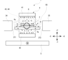
図22Aおよび図22Bを参照して、本発明の第2の実施の形態としての電流センサ6の構成について説明する。図22Aは、電流センサ6の全体構成例を表す斜視図である。図22Aに示したように、電流センサ6は、例えば磁気検出部7と、集磁コア8と、磁気シールド9と、導体10とを有する。
<2. Second Embodiment>
[Configuration of current sensor 6]
A configuration of current sensor 6 as a second embodiment of the present invention will be described with reference to FIGS. 22A and 22B. 22A is a perspective view showing an example of the overall configuration of the current sensor 6. FIG. As shown in FIG. 22A, the current sensor 6 has, for example, a magnetic detector 7, a magnetism collection core 8, a magnetic shield 9, and a conductor 10. As shown in FIG.

(導体10)
導体10は、例えば第1部分11と第2部分12と、第3部分13と、第4部分14と、第5部分15とが順に連結されたものである。導体10は、例えばCu(銅)などの高導電性非磁性材料により構成される。第1部分11、第3部分13、および第5部分15は、例えばXY面に沿って広がっている。第2部分12および第4部分14は、第1部分11、第3部分13、および第5部分15に対して立設するように、XZ面に沿って広がっている。第2~第4部分12~14は、折り返し部分を構成している。
なお、第2部分12が本発明の「第1導体部分」に対応する一具体例であり、第4部分14が本発明の「第2導体部分」に対応する一具体例である。
(Conductor 10)
The conductor 10 is formed by connecting, for example, a first portion 11, a second portion 12, a third portion 13, a fourth portion 14, and a fifth portion 15 in this order. The conductor 10 is made of a highly conductive non-magnetic material such as Cu (copper). The first portion 11, the third portion 13, and the fifth portion 15 extend, for example, along the XY plane. The second portion 12 and the fourth portion 14 extend along the XZ plane so as to stand with respect to the first portion 11 , the third portion 13 and the fifth portion 15 . The second to fourth portions 12 to 14 constitute folded portions.
The second portion 12 is a specific example corresponding to the "first conductor portion" of the present invention, and the fourth portion 14 is a specific example corresponding to the "second conductor portion" of the present invention.

(磁気検出部7)
磁気検出部7は、導体10の第2~第4部分12~14により構成される折り返し部分に形成される空間に配置されている。すなわち、磁気検出部7は、第2~第4部分12~14により取り囲まれた空間に配置されている。磁気検出部7の構成は、上記第1の実施の形態で説明した磁気検出部2の構成と実質的に同じものとすることができる。
(Magnetic detector 7)
The magnetic detection section 7 is arranged in a space formed in the folded portion formed by the second to fourth portions 12 to 14 of the conductor 10 . That is, the magnetic detector 7 is arranged in a space surrounded by the second to fourth portions 12-14. The configuration of the magnetic detection section 7 can be substantially the same as the configuration of the magnetic detection section 2 described in the first embodiment.

(磁気シールド9)
磁気シールド9は、YZ面に沿って磁気検出部7を取り囲む磁気遮蔽部材である。すなわち、磁気シールド9は、検出対象とする磁束Bm以外の外部からの不要な磁場(磁束)の、磁気検出部7に対する影響を緩和する軟磁性体である。磁気シールド9は、導体10の第2~第4部分12~14により取り囲まれた空間に配置されている。さらに、磁気シールド9は、集磁コア8によって取り囲まれた空間に配置されている。図22Bは、図22Aに示した電流センサ6のうちの磁気シールド9の構成例を表すYZ面に沿った平面図である。磁気シールド9の構成は、上記第1の実施の形態で説明した磁気シールド4の構成と実質的に同じものとすることができる。具体的には、図22Bに示したように、磁気シールド9は、X軸方向と直交するYZ面に沿って磁気検出部7を取り囲むように、全体として環状の形状を有している。なお、磁気検出部7を取り囲むとは、磁気検出部7の周囲の周回するように環状をなしている形態のみならず、磁気検出部7の周囲のうちの一部と対向する部分が欠落した状態の切り欠きを含む形態をも概念である。磁気シールド9は、導体10および磁気検出部7の双方と物理的に接触せずに離間して配置されている。
(Magnetic shield 9)
The magnetic shield 9 is a magnetic shielding member that surrounds the magnetic detector 7 along the YZ plane. In other words, the magnetic shield 9 is a soft magnetic material that mitigates the influence of an unnecessary external magnetic field (magnetic flux) other than the magnetic flux Bm to be detected on the magnetic detection section 7 . A magnetic shield 9 is arranged in a space surrounded by the second to fourth portions 12 to 14 of the conductor 10 . Furthermore, the magnetic shield 9 is arranged in the space surrounded by the magnetic collecting core 8 . 22B is a plan view along the YZ plane showing a configuration example of the magnetic shield 9 of the current sensor 6 shown in FIG. 22A. The configuration of the magnetic shield 9 can be substantially the same as the configuration of the magnetic shield 4 described in the first embodiment. Specifically, as shown in FIG. 22B, the magnetic shield 9 has an annular shape as a whole so as to surround the magnetic detection section 7 along the YZ plane perpendicular to the X-axis direction. In addition, "surrounding the magnetic detection unit 7" means not only a form in which the magnetic detection unit 7 is surrounded by an annular shape, but also a part of the circumference of the magnetic detection unit 7 that faces a part is missing. It is also a concept to have a form that includes a state notch. The magnetic shield 9 is spaced apart from both the conductor 10 and the magnetic detection section 7 without physically contacting them.

磁気シールド9は、例えば第1シールド部91と、第2シールド部92と、第3シールド部93と、第4シールド部94とを含んでいる。第1シールド部91および第2シールド部92は、X軸方向およびY軸方向を含むXY面に沿って広がっている。第3シールド部93および第4シールド部94は、例えば導体10の第2部分12および第4部分14が延在するZ軸方向に延在している。第1シールド部91と第2シールド部92とは、Z軸方向において対向するように配置されている。第1シールド部91は、Z軸方向において例えば導体10のうちの第3部分13と磁気検出部7との間に配置される。第2シールド部92は、磁気検出部7から見て導体10の第3部分13の反対側に配置される。また、磁気検出部7は、XY面に直交するZ軸方向に眺めた状態で第1シールド部91および第2シールド部92の双方と重なり合うように配置されている。第3シールド部93と第4シールド部94とは、Y軸方向において対向するように配置されている。第3シールド部93は、第1シールド部91のY軸方向の第1端部911と、第2シールド部92のY軸方向の第1端部921とを磁気的に繋ぐように設けられている。第4シールド部94は、第1シールド部91のY軸方向の第1端部911と反対側の第2端部912と、第2シールド部92のY軸方向の第1端部921と反対側の第2端部922とを磁気的に繋ぐように設けられている。なお、図22Bでは、第1シールド部91と、第2シールド部92と、第3シールド部93と、第4シールド部94とが互いに物理的に接触するように連結されている場合を例示しているが、本実施の形態はこれに限定されるものではない。例えば第1シールド部91と、第2シールド部92と、第3シールド部93と、第4シールド部94とが物理的に接触していなくとも、互いに磁気的に連結されている状態であればよい。ここでいう磁気的に連結されている状態とは、例えば0.05mm以下の間隔となるように近接して配置されている状態をいう。互いに連結される2つのシールド部同士の間隔が例えば0.1mm以上であると、磁気的に分割され、磁気的なシールド効果が低減してしまう。
また、磁気シールド9は、本発明の「第1軟磁性体」に対応する一具体例である。また、第1~第4シールド部91~94は、それぞれ、本発明の「第1~第4部分」に対応する一具体例である。また、本実施の形態のZ軸方向は、本発明の「第1方向」に対応する一具体例である。また、本実施の形態のX軸方向は、本発明の「第2方向」に対応する一具体例である。また、本実施の形態のY軸方向は、本発明の「第3方向」に対応する一具体例である。また、本実施の形態のYZ面は、本発明の「第1平面」に対応する一具体例である。さらに、本実施の形態のXZ面は、本発明の「第2平面」に対応する一具体例である。
The magnetic shield 9 includes a first shield portion 91, a second shield portion 92, a third shield portion 93, and a fourth shield portion 94, for example. The first shield part 91 and the second shield part 92 spread along the XY plane including the X-axis direction and the Y-axis direction. The third shield part 93 and the fourth shield part 94 extend, for example, in the Z-axis direction along which the second portion 12 and the fourth portion 14 of the conductor 10 extend. The first shield part 91 and the second shield part 92 are arranged so as to face each other in the Z-axis direction. The first shield part 91 is arranged, for example, between the third part 13 of the conductor 10 and the magnetic detection part 7 in the Z-axis direction. The second shield part 92 is arranged on the opposite side of the third part 13 of the conductor 10 when viewed from the magnetic detection part 7 . The magnetic detection section 7 is arranged so as to overlap both the first shield section 91 and the second shield section 92 when viewed in the Z-axis direction perpendicular to the XY plane. The third shield part 93 and the fourth shield part 94 are arranged so as to face each other in the Y-axis direction. The third shield portion 93 is provided so as to magnetically connect the first end portion 911 of the first shield portion 91 in the Y-axis direction and the first end portion 921 of the second shield portion 92 in the Y-axis direction. there is The fourth shield part 94 has a second end 912 opposite to the first end 911 in the Y-axis direction of the first shield part 91 and a first end 921 in the Y-axis direction of the second shield part 92 . It is provided so as to be magnetically connected to the second end 922 on the side. Note that FIG. 22B illustrates a case where the first shield part 91, the second shield part 92, the third shield part 93, and the fourth shield part 94 are connected so as to physically contact each other. However, the present embodiment is not limited to this. For example, even if the first shield part 91, the second shield part 92, the third shield part 93, and the fourth shield part 94 are not in physical contact, if they are magnetically connected to each other, good. The state of being magnetically coupled here means the state of being arranged close to each other with an interval of 0.05 mm or less, for example. If the distance between the two shield portions that are connected to each other is, for example, 0.1 mm or more, they will be magnetically divided and the magnetic shielding effect will be reduced.
Also, the magnetic shield 9 is a specific example corresponding to the "first soft magnetic body" of the present invention. Also, the first to fourth shield portions 91 to 94 are specific examples corresponding to the "first to fourth portions" of the present invention, respectively. Also, the Z-axis direction in the present embodiment is a specific example corresponding to the "first direction" of the invention. Also, the X-axis direction in the present embodiment is a specific example corresponding to the "second direction" of the invention. Also, the Y-axis direction in this embodiment is a specific example corresponding to the "third direction" of the present invention. Also, the YZ plane of the present embodiment is a specific example corresponding to the "first plane" of the invention. Furthermore, the XZ plane of this embodiment is a specific example corresponding to the "second plane" of the present invention.

(集磁コア8)
集磁コア8は、自らを磁束Bmが通過するように磁束Bmを集束する軟磁性体である。集磁コア8は、例えばY軸方向と直交するXZ面に沿って磁気検出部7、磁気シールド9、ならびに導体10の第2部分12および第4部分14を取り囲むように設けられている。集磁コア8の構成材料は、上記第1の実施の形態で説明した集磁コア3の構成材料と実質的に同じものとすることができる。
なお、集磁コア8は、本発明の「第2軟磁性体」に対応する一具体例である。また、本実施の形態のXY面は、本発明の「第3平面」に対応する一具体例である。
(Magnetic collection core 8)
The magnetic collecting core 8 is a soft magnetic material that collects the magnetic flux Bm so that the magnetic flux Bm passes through itself. The magnetic collecting core 8 is provided so as to surround the magnetic detecting section 7, the magnetic shield 9, and the second portion 12 and the fourth portion 14 of the conductor 10, for example, along the XZ plane perpendicular to the Y-axis direction. The constituent material of the magnetism collecting core 8 can be substantially the same as the constituent material of the magnetism collecting core 3 described in the first embodiment.
The magnet collecting core 8 is a specific example corresponding to the "second soft magnetic body" of the present invention. Also, the XY plane of the present embodiment is a specific example corresponding to the "third plane" of the present invention.

集磁コア8および磁気シールド9は、例えば、珪素鋼、電磁鋼、純鉄(SUY)、パーマロイ等の軟磁性材料を主たる構成材料として含んでいる。集磁コア8は、磁気シールド9と比べて磁束Bmの印加により着磁されやすいので、比較的残留磁化が小さい材料であるFeSiやパーマロイにより構成されるとよい。一方、磁気シールド9は集磁コア8と比べて磁束Bmによる着磁がなされにくいので、比較的残留磁化が大きい材料である純鉄Fなどを用いることができる。 The magnetic collecting core 8 and the magnetic shield 9 contain, for example, soft magnetic materials such as silicon steel, electromagnetic steel, pure iron (SUY), permalloy, etc. as main constituent materials. Since the magnetic collecting core 8 is more likely to be magnetized by applying the magnetic flux Bm than the magnetic shield 9, it is preferably made of FeSi or permalloy, which is a material with relatively small residual magnetization. On the other hand, since the magnetic shield 9 is less likely to be magnetized by the magnetic flux Bm than the magnetic collecting core 8, pure iron F or the like, which is a material with relatively large residual magnetization, can be used.

また、磁気シールド9の構成材料の鉄損は、例えば集磁コア8の構成材料の鉄損よりも大きいことが望ましい。 Further, it is desirable that the core loss of the material forming the magnetic shield 9 is greater than the core loss of the material forming the magnetic collecting core 8, for example.

[電流センサ6の作用効果]
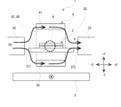
図23は、電流センサ6を-Z方向に眺めた状態の、XY面に沿った断面図である。 電流センサ6では、導体10の第2部分12を電流Imが+Zの向きに流れると、第2部分12の周囲には磁束Bm1が発生する。磁束Bm1は、磁気検出部7に対し、X軸方向に沿った-Xの向きに付与される。電流Imは、第2部分12から第3部分13を経由して第4部分14を-Zの向きに流れる。そのため、第4部分14の周囲には磁束Bm2が発生する。磁束Bm2は、磁気検出部7に対し、X軸方向に沿った-Xの向きに付与される。したがって、磁気検出部7の近傍では、磁束Bm1と磁束Bm2とが合成されて高密度の磁束Bmが発生し、磁気検出部7に付与される。したがって、電流センサ6によれば、比較的微弱な電流Imであっても高い感度で電流値を検出することができる。
[Action and effect of current sensor 6]
FIG. 23 is a cross-sectional view along the XY plane when the current sensor 6 is viewed in the -Z direction. In the current sensor 6 , when the current Im flows through the second portion 12 of the conductor 10 in the +Z direction, a magnetic flux Bm1 is generated around the second portion 12 . The magnetic flux Bm1 is applied to the magnetic detection section 7 in the -X direction along the X-axis direction. The current Im flows from the second portion 12 through the third portion 13 and then through the fourth portion 14 in the -Z direction. Therefore, a magnetic flux Bm2 is generated around the fourth portion 14 . The magnetic flux Bm2 is applied to the magnetic detection section 7 in the -X direction along the X-axis direction. Therefore, in the vicinity of the magnetic detection section 7, the magnetic flux Bm1 and the magnetic flux Bm2 are synthesized to generate a high-density magnetic flux Bm, which is applied to the magnetic detection section 7. FIG. Therefore, according to the current sensor 6, even a relatively weak current Im can be detected with high sensitivity.

電流センサ6によれば、磁気検出部7を取り囲むように磁気シールド9を設けるようにしている。このため、磁気検出部7に対する、周囲からの不要な外乱磁場の磁束の影響が緩和される。よって、電流センサ6では、磁束Bmを高い精度で検出し、導体10を流れる電流Imの大きさを高い精度で測定することができる。 According to the current sensor 6 , the magnetic shield 9 is provided so as to surround the magnetic detection section 7 . Therefore, the influence of the magnetic flux of the unwanted disturbance magnetic field from the surroundings on the magnetic detection section 7 is alleviated. Therefore, the current sensor 6 can detect the magnetic flux Bm with high accuracy and measure the magnitude of the current Im flowing through the conductor 10 with high accuracy.

(変形例2-1)
図24は、上記第2の実施の形態の第1変形例(変形例2-1)としての電流センサ6Aの外観を表す斜視図である。第2の実施の形態の電流センサ6では、磁気検出部7の周囲を周回する環状をなす磁気シールド9を有するようにした。これに対し、変形例2-1の電流センサ6Aでは、図24に示したように磁気シールド9の代わりに磁気シールド9Aを有する。磁気シールド9Aは、環状の一部に切り欠きK9Aを含んでおり、YZ面において一部が開放されたU形状を有している。変形例2-1の電流センサ6Aにおいても、磁気シールド9Aを有しているので、磁気シールド9Aを含まない場合と比較して磁気検出部7に対する外乱磁場の影響を低減することができる。
(Modification 2-1)
FIG. 24 is a perspective view showing the appearance of a current sensor 6A as a first modification (modification 2-1) of the second embodiment. The current sensor 6 of the second embodiment is provided with an annular magnetic shield 9 encircling the magnetic detection section 7 . On the other hand, the current sensor 6A of Modification 2-1 has a magnetic shield 9A instead of the magnetic shield 9 as shown in FIG. The magnetic shield 9A includes a notch K9A in a part of the ring shape, and has a U shape that is partially open on the YZ plane. Since the current sensor 6A of the modified example 2-1 also has the magnetic shield 9A, the influence of the disturbance magnetic field on the magnetic detection section 7 can be reduced as compared with the case where the magnetic shield 9A is not included.

<3.第3の実施の形態>
図25は、電流センサ1などを備えた電気制御装置の構成例を表すブロック図である。上記第1の実施の形態およびいくつかの変形例、ならびに第2の実施の形態および変形例で説明した電流センサ1,1A~1J,6,6Aは、いずれも、例えば図25に示した電気制御装置110に搭載することができる。
<3. Third Embodiment>
FIG. 25 is a block diagram showing a configuration example of an electric control device including the current sensor 1 and the like. All of the current sensors 1, 1A to 1J, 6, 6A described in the first embodiment and some modifications, and the second embodiment and modifications are, for example, electric current sensors shown in FIG. It can be mounted on the control device 110 .

電気制御装置110は、例えば電流センサ111と、電源装置112と、制御回路113とを備える。電流センサ111は、電源装置112から出力され、あるいは電源装置112に入力される電流を測定するようになっている。電流センサ111において測定された電流値に関する情報は、制御回路113に送信されるようになっている。制御回路113は、例えば電流センサ111の動作および電源装置112の動作を制御する装置である。制御回路113は、例えば電流センサ111からの情報に基づいて電源装置112からの出力電流の調整を行う。電流センサ111には、上記実施の形態等で説明した電流センサ1,1A~1J,6,6Aを適用することができる。なお、本発明の電気制御装置としては、例えば、ハイブリッド電気自動車(HEV: Hybrid Electric Vehicle)や電気自動車(EV: Electric Vehicle)等のバッテリマネジメントシステム、インバータ及びコンバータ等が挙げられる。 The electrical control device 110 includes, for example, a current sensor 111 , a power supply device 112 and a control circuit 113 . The current sensor 111 measures the current output from the power supply device 112 or the current input to the power supply device 112 . Information about the current value measured by the current sensor 111 is transmitted to the control circuit 113 . The control circuit 113 is a device that controls the operation of the current sensor 111 and the operation of the power supply device 112, for example. The control circuit 113 adjusts the output current from the power supply device 112 based on information from the current sensor 111, for example. As the current sensor 111, the current sensors 1, 1A to 1J, 6, 6A described in the above embodiments and the like can be applied. Examples of the electric control device of the present invention include battery management systems, inverters and converters for hybrid electric vehicles (HEVs) and electric vehicles (EVs).

以上説明した実施形態および変形例は、本発明の理解を容易にするために記載されたものであって、本発明を限定するために記載されたものではない。したがって、上記実施形態等に開示された各要素は、本発明の技術的範囲に属する全ての設計変更や均等物をも含む趣旨である。すなわち、本発明は上記実施の形態等に限定されるものではなく、種々の変形が可能である。 The embodiments and modifications described above are described to facilitate understanding of the present invention, and are not described to limit the present invention. Therefore, each element disclosed in the above embodiments and the like is meant to include all design changes and equivalents that fall within the technical scope of the present invention. That is, the present invention is not limited to the above embodiments and the like, and various modifications are possible.

1,6…電流センサ、2,7…磁気検出部、3,8…集磁コア、3T1,3T2…端面、31…第1コア部、32…第2コア部、33…第3コア部、34…第4コア部、35…第5コア部、4,9…磁気シールド、41,91…第1シールド部、42,92…第2シールド部、43,93…第3シールド部、44,94…第4シールド部、5,10…導体、Bm…磁束、CG…コアギャップ、Im…電流。 Reference Signs List 1, 6 Current sensor 2, 7 Magnetic detector 3, 8 Magnetism collecting core 3T1, 3T2 End face 31 First core 32 Second core 33 Third core 34... fourth core portion, 35... fifth core portion, 4, 9... magnetic shield, 41, 91... first shield portion, 42, 92... second shield portion, 43, 93... third shield portion, 44, 94... Fourth shield part, 5, 10... Conductor, Bm... Magnetic flux, CG... Core gap, Im... Current.

Claims (19)

導体を第1方向に沿って流れる電流により発生する第2方向の磁束が付与される磁気検出部と、
第1部分と、前記導体と前記第1部分との間に配置される第2部分と、前記第1部分と前記第2部分とを磁気的に繋ぐ第3部分とを含み、前記導体および前記磁気検出部の双方と離間しつつ、前記第2方向と直交する第1平面に沿って前記磁気検出部を前記第1部分、前記第2部分および前記第3部分により取り囲む第1軟磁性体と、
前記第1方向と直交する第3平面に沿って前記導体を取り囲む第2軟磁性体と
を有し、
前記第2軟磁性体は、前記第2方向に互いに離間して対向する第1端面および第2端面を含み、
前記磁気検出部は、前記第1端面と前記第2端面との隙間に配置されており、
前記第1軟磁性体は、前記第1方向および前記第2方向を含む第2平面に対して実質的に直交する第3方向において前記第2軟磁性体と重なり合うことなく、前記第2方向における前記第1端面と前記第2端面との間の領域に設けられている
電流センサ。
a magnetic detection unit to which a magnetic flux in a second direction generated by a current flowing through the conductor along the first direction is applied;
a first portion, a second portion disposed between the conductor and the first portion, and a third portion magnetically connecting the first portion and the second portion; a first soft magnetic body that surrounds the magnetic detection section with the first portion, the second portion, and the third portion along a first plane orthogonal to the second direction while being spaced apart from both of the magnetic detection portions ; ,
a second soft magnetic body surrounding the conductor along a third plane perpendicular to the first direction;
has
The second soft magnetic body includes a first end face and a second end face that are spaced apart and face each other in the second direction,
The magnetic detection unit is arranged in a gap between the first end face and the second end face,
The first soft magnetic body does not overlap the second soft magnetic body in a third direction substantially orthogonal to a second plane including the first direction and the second direction, and provided in a region between the first end face and the second end face
current sensor.
前記第1部分および前記第2部分は、前記第1方向および前記第2方向を含む第2平面に沿って広がっている
請求項1記載の電流センサ。
2. The current sensor of claim 1, wherein said first portion and said second portion extend along a second plane including said first direction and said second direction.
前記第3部分は、前記第2平面に対して実質的に直交する第3方向に延在している
請求項2記載の電流センサ。
3. The current sensor of claim 2, wherein said third portion extends in a third direction substantially orthogonal to said second plane.
前記磁気検出部は、前記第1方向および前記第2方向を含む第2平面に直交する第3方向に眺めた状態で前記第1部分および前記第2部分の双方と重なり合うように配置されている
請求項1から請求項3のいずれか1項に記載の電流センサ。
The magnetic detection section is arranged so as to overlap both the first portion and the second portion when viewed in a third direction orthogonal to a second plane including the first direction and the second direction. The current sensor according to any one of claims 1 to 3.
前記第1部分および前記第2部分は、それぞれ、前記第1方向の両端部である第1端部および第2端部を含み、
前記第3部分は、前記第1部分の前記第1端部と前記第2部分の前記第1端部とを磁気的に繋ぐように設けられている
請求項1から請求項4のいずれか1項に記載の電流センサ。
The first portion and the second portion each include a first end and a second end, which are both ends in the first direction,
5. The third portion is provided so as to magnetically connect the first end of the first portion and the first end of the second portion. A current sensor as described above.
前記第1軟磁性体は、
前記第1部分の前記第2端部と前記第2部分の前記第2端部とを磁気的に繋ぐように設けられると共に前記第1方向において前記第3部分と対向する第4部分をさらに有する
請求項5記載の電流センサ。
The first soft magnetic body is
further comprising a fourth portion provided to magnetically connect the second end of the first portion and the second end of the second portion and facing the third portion in the first direction; The current sensor according to claim 5.
前記第1軟磁性体の主たる構成材料である第1構成材料の鉄損は、前記第2軟磁性体の主たる構成材料である第2構成材料の鉄損よりも大きい
請求項1から請求項6のいずれか1項に記載の電流センサ。
The iron loss of the first constituent material, which is the main constituent material of the first soft magnetic body, is greater than the iron loss of the second constituent material, which is the main constituent material of the second soft magnetic body.
The current sensor according to any one of claims 1 to 6 .
導体を第1方向に沿って流れる電流により発生する第2方向の磁束が付与される磁気検出部と、a magnetic detection unit to which a magnetic flux in a second direction generated by a current flowing through the conductor along the first direction is applied;
第1部分と、前記導体と前記第1部分との間に配置される第2部分と、前記第1部分と前記第2部分とを磁気的に繋ぐ第3部分とを含み、前記導体および前記磁気検出部の双方と離間しつつ、前記第2方向と直交する第1平面に沿って前記磁気検出部を前記第1部分、前記第2部分および前記第3部分により取り囲む第1軟磁性体とa first portion, a second portion disposed between the conductor and the first portion, and a third portion magnetically connecting the first portion and the second portion; a first soft magnetic body that surrounds the magnetic detection section with the first portion, the second portion, and the third portion along a first plane orthogonal to the second direction while being spaced apart from both of the magnetic detection portions;
を有し、has
前記第1部分および前記第2部分は、それぞれ、前記第1方向の両端部である第1端部および第2端部を含み、The first portion and the second portion each include a first end and a second end, which are both ends in the first direction,
前記第3部分は、前記第1部分の前記第1端部と前記第2部分の前記第1端部とを磁気的に繋ぐように設けられており、the third portion is provided to magnetically connect the first end of the first portion and the first end of the second portion;
前記第1部分の前記第2端部と前記第2部分の前記第2端部とが物理的に離間しているthe second end of the first portion and the second end of the second portion are physically separated
電流センサ。current sensor.
導体を第1方向に沿って流れる電流により発生する第2方向の磁束が付与される磁気検出部と、a magnetic detection unit to which a magnetic flux in a second direction generated by a current flowing through the conductor along the first direction is applied;
第1部分と、前記導体と前記第1部分との間に配置される第2部分と、前記第1部分と前記第2部分とを磁気的に繋ぐ第3部分とを含み、前記導体および前記磁気検出部の双方と離間しつつ、前記第2方向と直交する第1平面に沿って前記磁気検出部を前記第1部分、前記第2部分および前記第3部分により取り囲む第1軟磁性体と、a first portion, a second portion disposed between the conductor and the first portion, and a third portion magnetically connecting the first portion and the second portion; a first soft magnetic body that surrounds the magnetic detection section with the first portion, the second portion, and the third portion along a first plane orthogonal to the second direction while being spaced apart from both of the magnetic detection portions; ,
前記第1方向と直交する第3平面に沿って前記導体を取り囲む第2軟磁性体とa second soft magnetic body surrounding the conductor along a third plane perpendicular to the first direction;
を有し、has
前記第1軟磁性体の主たる構成材料である第1構成材料の鉄損は、前記第2軟磁性体の主たる構成材料である第2構成材料の鉄損よりも大きいThe iron loss of the first constituent material, which is the main constituent material of the first soft magnetic body, is greater than the iron loss of the second constituent material, which is the main constituent material of the second soft magnetic body.
電流センサ。current sensor.
磁気検出部と、
第1方向に延在し、電流が第1の向きに流れることにより前記磁気検出部に対し第2方向に付与される第1磁束を発生する第1導体部分と、前記第1方向に延在し、前記電流が前記第1の向きと反対の第2の向きに流れることにより前記磁気検出部に対し前記第2方向に付与される第2磁束を発生する第2導体部分とを含む導体と、
1部分と、前記第1方向において前記第1部分と対向するように配置された第2部分と、前記第1部分と前記第2部分とを磁気的に繋ぐ第3部分とを含み、前記導体および前記磁気検出部の双方と離間しつつ、前記第2方向と直交する第1平面に沿って前記磁気検出部を前記第1部分、前記第2部分および前記第3部分により取り囲む第1軟磁性体と、
前記第1方向と直交する第3平面に沿って前記磁気検出部、前記第1導体部分および前記第2導体部分を取り囲む第2軟磁性体とを
有する
電流センサ。
a magnetic detection unit;
a first conductor portion that extends in a first direction and generates a first magnetic flux that is applied in a second direction to the magnetic detection portion by current flowing in the first direction; and a first conductor portion that extends in the first direction. and a second conductor portion that generates a second magnetic flux that is applied to the magnetic detection section in the second direction when the current flows in the second direction opposite to the first direction; ,
a first portion, a second portion arranged to face the first portion in the first direction, and a third portion magnetically connecting the first portion and the second portion; A first soft body that surrounds the magnetic detection unit with the first portion, the second portion, and the third portion along a first plane orthogonal to the second direction while being spaced apart from both the conductor and the magnetic detection unit. a magnetic body;
A current sensor comprising: a second soft magnetic body surrounding the magnetic detecting portion, the first conductor portion, and the second conductor portion along a third plane orthogonal to the first direction.
前記磁気検出部は、前記第1方向に眺めた状態で前記第1部分および前記第2部分の双方と重なり合うように配置されている
請求項10記載の電流センサ。
The current sensor according to claim 10, wherein the magnetic detector is arranged so as to overlap both the first portion and the second portion when viewed in the first direction.
前記第3部分は、前記第1方向に延在している
請求項10または請求項11に記載の電流センサ。
The current sensor according to claim 10 or 11, wherein the third portion extends in the first direction.
前記第1部分および前記第2部分は、それぞれ、前記第1方向および前記第2方向を含む第2平面に対して実質的に直交する第3方向の両端部である第1端部および第2端部を含み、
前記第3部分は、前記第1部分の前記第1端部と前記第2部分の前記第1端部とを磁気的に繋ぐように設けられている
請求項10から請求項12のいずれか1項に記載の電流センサ。
The first portion and the second portion are respectively a first end portion and a second portion, which are both ends in a third direction substantially orthogonal to a second plane including the first direction and the second direction. including ends,
13. Any one of claims 10 to 12, wherein the third portion is provided to magnetically connect the first end of the first portion and the first end of the second portion. A current sensor as described above.
前記第1軟磁性体は、
前記第1部分の前記第2端部と前記第2部分の前記第2端部とを磁気的に繋ぐように設けられると共に前記第1方向において前記第3部分と対向する第4部分をさらに有する
請求項13記載の電流センサ。
The first soft magnetic body is
further comprising a fourth portion provided to magnetically connect the second end of the first portion and the second end of the second portion and facing the third portion in the first direction; 14. The current sensor of claim 13.
前記第1軟磁性体は、前記第2軟磁性体によって取り囲まれた空間に配置されている
請求項10から請求項14のいずれか1項に記載の電流センサ。
The current sensor according to any one of claims 10 to 14, wherein the first soft magnetic body is arranged in a space surrounded by the second soft magnetic body.
前記第1軟磁性体の主たる構成材料である第1構成材料の鉄損は、前記第2軟磁性体の主たる構成材料である第2構成材料の鉄損よりも大きい
請求項10から請求項15のいずれか1項に記載の電流センサ。
The iron loss of the first constituent material, which is the main constituent material of the first soft magnetic body, is greater than the iron loss of the second constituent material, which is the main constituent material of the second soft magnetic body. The current sensor according to any one of .
前記磁気検出部は、磁気抵抗効果素子またはホール素子を含む
請求項1から請求項16のいずれか1項に記載の電流センサ。
The current sensor according to any one of claims 1 to 16, wherein the magnetic detection section includes a magnetoresistive effect element or a Hall element.
前記磁気抵抗効果素子は、巨大磁気抵抗効果素子またはトンネル磁気抵抗効果素子である
請求項17記載の電流センサ。
The current sensor according to claim 17, wherein the magnetoresistive element is a giant magnetoresistive element or a tunnel magnetoresistive element.
請求項1から請求項18のいずれか1項に記載の電流センサを備えた電気制御装置。 An electric control device comprising a current sensor according to any one of claims 1 to 18.
JP2021013902A 2021-01-29 2021-01-29 Current sensor and electric control device with the same Active JP7243747B2 (en)

Priority Applications (4)

Application Number Priority Date Filing Date Title
JP2021013902A JP7243747B2 (en) 2021-01-29 2021-01-29 Current sensor and electric control device with the same
US17/517,341 US11543469B2 (en) 2021-01-29 2021-11-02 Current sensor, and electric control apparatus including the current sensor
DE102021129837.7A DE102021129837A1 (en) 2021-01-29 2021-11-16 CURRENT SENSOR, AND ELECTRICAL CONTROL UNIT WITH THE CURRENT SENSOR
CN202111412536.0A CN114814326A (en) 2021-01-29 2021-11-25 Current sensor and electric control device equipped with the same

Applications Claiming Priority (1)

Application Number Priority Date Filing Date Title
JP2021013902A JP7243747B2 (en) 2021-01-29 2021-01-29 Current sensor and electric control device with the same

Publications (2)

Publication Number Publication Date
JP2022117289A JP2022117289A (en) 2022-08-10
JP7243747B2 true JP7243747B2 (en) 2023-03-22

Family

ID=82402971

Family Applications (1)

Application Number Title Priority Date Filing Date
JP2021013902A Active JP7243747B2 (en) 2021-01-29 2021-01-29 Current sensor and electric control device with the same

Country Status (4)

Country Link
US (1) US11543469B2 (en)
JP (1) JP7243747B2 (en)
CN (1) CN114814326A (en)
DE (1) DE102021129837A1 (en)

Citations (3)

* Cited by examiner, † Cited by third party
Publication number Priority date Publication date Assignee Title
JP2013161773A (en) 2012-02-09 2013-08-19 Panasonic Corp Pole plate and secondary battery
JP2015132534A (en) 2014-01-14 2015-07-23 株式会社東海理化電機製作所 Current detection device
JP2015210272A (en) 2014-04-28 2015-11-24 タイコ エレクトロニクス アンプ コリア カンパニーTyco Electronics AMP Korea Co.,Ltd Hybrid current sensor assembly

Family Cites Families (17)

* Cited by examiner, † Cited by third party
Publication number Priority date Publication date Assignee Title
JPH0581731A (en) 1991-09-18 1993-04-02 Canon Inc Magnetic recording/reproducing device
JP3681584B2 (en) 1999-08-27 2005-08-10 矢崎総業株式会社 Current sensor and electric circuit using the same
JP2005055405A (en) * 2003-08-07 2005-03-03 Asahi Kasei Electronics Co Ltd Current sensor
JP4833111B2 (en) 2006-09-20 2011-12-07 株式会社東海理化電機製作所 Current detector
JP5417404B2 (en) * 2011-09-26 2014-02-12 トヨタ自動車株式会社 Current detector
DE112013002170T5 (en) 2012-04-23 2015-01-15 Hitachi Metals, Ltd. Magnetic sensor device
JP2013228315A (en) 2012-04-26 2013-11-07 Tdk Corp Current sensor
EP2942631B1 (en) 2014-04-28 2024-03-06 TYCO ELECTRONICS AMP KOREA Co., Ltd. Hybrid current sensor assembly
JP2015210247A (en) 2014-04-30 2015-11-24 日本電産サンキョー株式会社 Current sensor
JP6541962B2 (en) * 2014-12-17 2019-07-10 日置電機株式会社 Current sensor and measuring device
JP2016148620A (en) 2015-02-13 2016-08-18 株式会社フジクラ Current sensor
JP6711086B2 (en) * 2016-04-01 2020-06-17 日立金属株式会社 Current sensor
JP6596033B2 (en) * 2017-05-08 2019-10-23 矢崎総業株式会社 Current sensor
JP2018189504A (en) * 2017-05-08 2018-11-29 矢崎総業株式会社 Curent sensor
JP2019078542A (en) 2017-10-20 2019-05-23 トヨタ自動車株式会社 Current sensor
JP6890112B2 (en) * 2018-11-15 2021-06-18 矢崎総業株式会社 Current detector
JP2020165762A (en) 2019-03-29 2020-10-08 Tdk株式会社 Current sensor

Patent Citations (3)

* Cited by examiner, † Cited by third party
Publication number Priority date Publication date Assignee Title
JP2013161773A (en) 2012-02-09 2013-08-19 Panasonic Corp Pole plate and secondary battery
JP2015132534A (en) 2014-01-14 2015-07-23 株式会社東海理化電機製作所 Current detection device
JP2015210272A (en) 2014-04-28 2015-11-24 タイコ エレクトロニクス アンプ コリア カンパニーTyco Electronics AMP Korea Co.,Ltd Hybrid current sensor assembly

Also Published As

Publication number Publication date
DE102021129837A1 (en) 2022-08-04
JP2022117289A (en) 2022-08-10
CN114814326A (en) 2022-07-29
US20220244325A1 (en) 2022-08-04
US11543469B2 (en) 2023-01-03

Similar Documents

Publication Publication Date Title
JP5531215B2 (en) Current sensor
US10114044B2 (en) Current sensor
US9063185B2 (en) Current sensor
US8487612B2 (en) Current sensor
JP5411285B2 (en) Magnetic balanced current sensor
JP5906488B2 (en) Current sensor
WO2013005459A1 (en) Current sensor
JP5728719B2 (en) Current sensor
US20130057273A1 (en) Current sensor
JP6658676B2 (en) Current sensor
JP2009162499A (en) Magnetometric sensor
WO2012046547A1 (en) Current sensor
CN109407017B (en) Magnetic sensor
JP5505817B2 (en) Magnetic balanced current sensor
JP5487403B2 (en) Current sensor
JP7243747B2 (en) Current sensor and electric control device with the same
CN114114101B (en) Magnetic sensor, and position detection device and current sensor using the same
JP7367657B2 (en) Current sensor and electrical control device
JP2013142569A (en) Current sensor
WO2012035906A1 (en) Current sensor
JP7215451B2 (en) CURRENT SENSOR AND MANUFACTURING METHOD THEREOF, ELECTRICAL CONTROL DEVICE, AND CURRENT SENSOR DESIGN METHOD
WO2015046206A1 (en) Current sensor
CN113376422B (en) Current sensor for improving functional safety

Legal Events

Date Code Title Description
A621 Written request for application examination

Free format text: JAPANESE INTERMEDIATE CODE: A621

Effective date: 20211130

A131 Notification of reasons for refusal

Free format text: JAPANESE INTERMEDIATE CODE: A131

Effective date: 20220830

A521 Request for written amendment filed

Free format text: JAPANESE INTERMEDIATE CODE: A523

Effective date: 20221031

TRDD Decision of grant or rejection written
A01 Written decision to grant a patent or to grant a registration (utility model)

Free format text: JAPANESE INTERMEDIATE CODE: A01

Effective date: 20230207

A61 First payment of annual fees (during grant procedure)

Free format text: JAPANESE INTERMEDIATE CODE: A61

Effective date: 20230220

R150 Certificate of patent or registration of utility model

Ref document number: 7243747

Country of ref document: JP

Free format text: JAPANESE INTERMEDIATE CODE: R150