JP7238506B2 - Wavelength conversion element, light source device and projector - Google Patents
Wavelength conversion element, light source device and projector Download PDFInfo
- Publication number
- JP7238506B2 JP7238506B2 JP2019050086A JP2019050086A JP7238506B2 JP 7238506 B2 JP7238506 B2 JP 7238506B2 JP 2019050086 A JP2019050086 A JP 2019050086A JP 2019050086 A JP2019050086 A JP 2019050086A JP 7238506 B2 JP7238506 B2 JP 7238506B2
- Authority
- JP
- Japan
- Prior art keywords
- phosphor
- binder
- light
- wavelength conversion
- layer
- Prior art date
- Legal status (The legal status is an assumption and is not a legal conclusion. Google has not performed a legal analysis and makes no representation as to the accuracy of the status listed.)
- Active
Links
Images


Classifications
-
- G—PHYSICS
- G03—PHOTOGRAPHY; CINEMATOGRAPHY; ANALOGOUS TECHNIQUES USING WAVES OTHER THAN OPTICAL WAVES; ELECTROGRAPHY; HOLOGRAPHY
- G03B—APPARATUS OR ARRANGEMENTS FOR TAKING PHOTOGRAPHS OR FOR PROJECTING OR VIEWING THEM; APPARATUS OR ARRANGEMENTS EMPLOYING ANALOGOUS TECHNIQUES USING WAVES OTHER THAN OPTICAL WAVES; ACCESSORIES THEREFOR
- G03B21/00—Projectors or projection-type viewers; Accessories therefor
- G03B21/14—Details
- G03B21/20—Lamp housings
- G03B21/2006—Lamp housings characterised by the light source
- G03B21/2033—LED or laser light sources
- G03B21/204—LED or laser light sources using secondary light emission, e.g. luminescence or fluorescence
Description
本発明は、波長変換素子、光源装置及びプロジェクターに関する。 The present invention relates to a wavelength conversion element, a light source device and a projector.
従来、入射される励起光によって励起され、励起光の波長より長い波長を有する蛍光を出射する波長変換素子が知られている。このような波長変換素子として、基材と、基材の表面に形成された反射層と、反射層上に形成された蛍光体層と、を備えた発光素子が知られている(例えば、特許文献1参照)。 2. Description of the Related Art Conventionally, there has been known a wavelength conversion element that is excited by incident excitation light and emits fluorescence having a wavelength longer than the wavelength of the excitation light. As such a wavelength conversion element, a light emitting element including a base material, a reflective layer formed on the surface of the base material, and a phosphor layer formed on the reflective layer is known (for example, patent Reference 1).
特許文献1に記載の発光素子では、蛍光体層は、複数の蛍光体粒子と、複数の蛍光体粒子を結合させるバインダーと、を有する。
バインダーは、例えば水ガラス等の無機材料の架橋体を含むものである。バインダーは、互いに隣り合う一の蛍光体粒子と他の一の蛍光体粒子とを結合するとともに、蛍光体粒子と反射層の表面とを結合する。蛍光体粒子は、外部から照射される励起光を吸収して蛍光を発する粒子状の蛍光体である。蛍光体粒子には、例えばYAG系材料の蛍光物質が含まれている。そして、特許文献1では、上記発光素子を有する光源装置が、プロジェクターに適用された例が示されている。
In the light-emitting device described in
The binder includes, for example, a crosslinked body of an inorganic material such as water glass. The binder binds one phosphor particle and another phosphor particle adjacent to each other, and also binds the phosphor particles and the surface of the reflective layer. The phosphor particles are particulate phosphors that absorb excitation light irradiated from the outside and emit fluorescence. The phosphor particles contain, for example, a YAG-based phosphor.
特許文献1に記載の蛍光体層では、複数の蛍光体粒子は、バインダー内に封入されている。換言すると、バインダーは、蛍光体粒子の表面全体を覆うように、蛍光体粒子の周囲に存在する。このため、蛍光体粒子から出射された蛍光は、バインダー内に入射され、バインダー内を伝播して、蛍光体層から出射される。蛍光体層から出射された蛍光は、光源装置から出射され、光学系を構成する反射型液晶パネルに入射される。
しかしながら、蛍光体層においてバインダー内を蛍光が伝播すると、蛍光体層の表面における蛍光の出射領域は、励起光の入射領域より大きくなる。そして、蛍光の出射領域が大きいと、光学系において液晶パネルに対する蛍光の入射効率が低下するおそれがある。すなわち、蛍光体粒子の表面全体がバインダーによって覆われていると、蛍光体層から蛍光が入射される光学系での蛍光の利用効率が低下するおそれがある。
In the phosphor layer described in
However, when fluorescence propagates through the binder in the phosphor layer, the fluorescence emission area on the surface of the phosphor layer becomes larger than the excitation light incidence area. In addition, if the fluorescence emission area is large, there is a possibility that the fluorescence incidence efficiency with respect to the liquid crystal panel in the optical system may decrease. That is, if the entire surface of the phosphor particles is covered with the binder, there is a possibility that the utilization efficiency of the fluorescence in the optical system in which the fluorescence is incident from the phosphor layer is lowered.
一方、波長変換素子においては、蛍光体層に照射された励起光のうち、一部の励起光が蛍光体粒子にて蛍光に変換されずに戻ってしまう後方散乱(バックスキャッタ)と呼ばれる現象が生じうる。このような励起光の光量が多くなると、励起光の波長変換効率が低下するという問題がある。 On the other hand, in the wavelength conversion element, a phenomenon called back scattering occurs in which part of the excitation light emitted to the phosphor layer returns without being converted into fluorescence by the phosphor particles. can occur. When the light quantity of such excitation light increases, there is a problem that the wavelength conversion efficiency of the excitation light decreases.
本発明の第1態様に係る波長変換素子は、複数の蛍光体粒子と、前記複数の蛍光体粒子のうち互いに隣り合う一方の蛍光体粒子と他方の蛍光体粒子とを結合するバインダーとを有する蛍光体層と、前記蛍光体層に対する励起光の入射側に設けられる反射防止層と、前記蛍光体層が設けられる基板と、を備え、前記バインダーは、ガラスを含有し、前記バインダーは、前記一方の蛍光体粒子の表面の一部と前記他方の蛍光体粒子の表面の一部とを結合することを特徴とする。 A wavelength conversion element according to a first aspect of the present invention includes a plurality of phosphor particles, and a binder that binds one of the plurality of phosphor particles and the other phosphor particles that are adjacent to each other. A phosphor layer, an antireflection layer provided on an excitation light incident side of the phosphor layer, and a substrate provided with the phosphor layer, wherein the binder contains glass, and the binder contains the above A part of the surface of one phosphor particle and a part of the surface of the other phosphor particle are bonded.
本発明の第2態様に係る波長変換素子は、複数の蛍光体粒子と、前記複数の蛍光体粒子のうち互いに隣り合う一方の蛍光体粒子と他方の蛍光体粒子とを結合するバインダーと、前記複数の蛍光体粒子の表面に設けられる反射防止層と、を有する蛍光体層と、前記蛍光体層が設けられる基板と、を備え、前記バインダーは、ガラスを含有し、前記バインダーは、前記一方の蛍光体粒子の表面の一部と前記他方の蛍光体粒子の表面の一部との間、前記一方の蛍光体粒子の表面に設けられた前記反射防止層と前記他方の蛍光体粒子の表面に設けられた前記反射防止層との間、及び、前記一方の蛍光体粒子の表面の一部と前記他方の蛍光体粒子の表面に設けられた前記反射防止層との間、の少なくともいずれかを結合することを特徴とする。 A wavelength conversion element according to a second aspect of the present invention includes: a plurality of phosphor particles; a binder that binds one of the plurality of phosphor particles and the other phosphor particles that are adjacent to each other; a phosphor layer having an antireflection layer provided on the surface of a plurality of phosphor particles; and a substrate on which the phosphor layer is provided, wherein the binder contains glass, and the binder between a part of the surface of the phosphor particle and a part of the surface of the other phosphor particle, the antireflection layer provided on the surface of the one phosphor particle and the surface of the other phosphor particle and between a part of the surface of the one phosphor particle and the antireflection layer provided on the surface of the other phosphor particle, at least one of are combined.
上記第1及び第2態様では、前記蛍光体粒子の体積の合計と前記バインダーの体積の合計とを合計した体積に対する前記バインダーの体積の割合は、0vol%より大きく、10vol%以下であることが好ましい。 In the first and second aspects, the ratio of the volume of the binder to the total volume of the total volume of the phosphor particles and the total volume of the binder is greater than 0 vol% and 10 vol% or less. preferable.
本発明の第3態様に係る光源装置は、上記波長変換素子と、前記波長変換素子に励起光を出射する光源と、を備えることを特徴とする。 A light source device according to a third aspect of the present invention includes the wavelength conversion element described above, and a light source that emits excitation light to the wavelength conversion element.
本発明の第4態様に係るプロジェクターは、上記光源装置と、前記光源装置から出射された光を画像情報に応じて変調する光変調装置と、前記光変調装置によって変調された光を投射する投射光学装置と、を備えることを特徴とする。 A projector according to a fourth aspect of the present invention includes the light source device, a light modulation device that modulates light emitted from the light source device according to image information, and a projector that projects the light modulated by the light modulation device. and an optical device.
[第1実施形態]
以下、本発明の第1実施形態について、図面に基づいて説明する。
[プロジェクターの概略構成]
図1は、本実施形態に係るプロジェクター1の構成を示す模式図である。
本実施形態に係るプロジェクター1は、後述する光源装置4から出射された光を変調して画像情報に応じた画像を形成する画像光を、スクリーン等の被投射面上に拡大投射する。プロジェクター1は、図1に示すように、外装を構成する外装筐体2と、外装筐体2内に配置される光源装置4及び光学装置30と、を備える。なお、光源装置4及び光学装置30の構成については、後に詳述する。この他、図示を省略するが、プロジェクター1は、プロジェクター1の動作を制御する制御装置、電子部品に電力を供給する電源装置、及び、冷却対象を冷却する冷却装置を備える。
[First embodiment]
A first embodiment of the present invention will be described below with reference to the drawings.
[Schematic configuration of the projector]
FIG. 1 is a schematic diagram showing the configuration of a
The
[外装筐体の構成]
外装筐体2は、それぞれ図示しない天面部及び底面部と、正面部21、背面部22、左側面部23及び右側面部24とを有し、略直方体形状に形成されている。
正面部21は、後述する投射光学装置36の一部を露出させる開口部211を有しており、投射光学装置36によって投射される画像光は、開口部211を通過する。また、正面部21は、プロジェクター1内の冷却対象を冷却した冷却気体が外装筐体2の外部に排出される排気口212を有する。更に、右側面部24は、外装筐体2外の気体を冷却気体として内部に導入する導入口241を有する。
[Configuration of exterior housing]
The
The
[光学装置の構成]
光学装置30は、均一化装置31、色分離装置32、リレー装置33、画像形成装置34、光学部品用筐体35及び投射光学装置36を備える。
均一化装置31は、光源装置4から出射された光を均一化する。均一化装置31によって均一化された光は、色分離装置32及びリレー装置33を経て、画像形成装置34の後述する光変調装置343の変調領域を照明する。均一化装置31は、2つのレンズアレイ311,312、偏光変換素子313及び重畳レンズ314を備える。
色分離装置32は、均一化装置31から入射される光を赤、緑及び青の各色光に分離する。色分離装置32は、2つのダイクロイックミラー321,322と、ダイクロイックミラー321によって分離された青色光を反射させる反射ミラー323と、を備える。
[Configuration of Optical Device]
The
The
The
リレー装置33は、青色光の光路及び緑色光の光路より長い赤色光の光路に設けられ、赤色光の損失を抑制する。リレー装置33は、入射側レンズ331、リレーレンズ333、反射ミラー332,334を備える。
なお、本実施形態では、赤色光の光路にリレー装置33を設けているが、これに限らず、例えば他の色光より光路が長い色光を青色光とし、青色光の光路上にリレー装置33を設ける構成としてもよい。
The
In this embodiment, the
画像形成装置34は、入射される赤、緑及び青の各色光を変調し、変調された各色光を合成して、投射光学装置36によって投射される画像光を形成する。画像形成装置34は、入射される各色光に応じて設けられる3つのフィールドレンズ341、3つの入射側偏光板342、3つの光変調装置343及び3つの出射側偏光板344と、1つの色合成装置345と、を備える。
光変調装置343は、光源装置4から出射された光を画像情報に応じて変調する。光変調装置343は、赤色光を変調する光変調装置343R、緑色光を変調する光変調装置343G、及び、青色光を変調する光変調装置343Bを含む。本実施形態では、光変調装置343は、透過型の液晶パネルによって構成されており、入射側偏光板342、光変調装置343及び出射側偏光板344によって液晶ライトバルブが構成される。
色合成装置345は、光変調装置343B,343G,343Rによって変調された各色光を合成して上記画像光を形成する。本実施形態では、色合成装置345は、クロスダイクロイックプリズムによって構成されているが、これに限らず、例えば複数のダイクロイックミラーによって構成することも可能である。
The
The
The
光学部品用筐体35は、それぞれ上記した均一化装置31、色分離装置32、リレー装置33及び画像形成装置34を内部に収容する。なお、光学装置30には、設計上の光軸である照明光軸Axが設定されており、光学部品用筐体35は、照明光軸Axにおける所定位置に均一化装置31、色分離装置32、リレー装置33及び画像形成装置34を保持する。光源装置4及び投射光学装置36は、照明光軸Axにおける所定位置に配置される。
The
投射光学装置36は、画像形成装置34から入射される画像光を被投射面上に拡大投射する。すなわち、投射光学装置36は、光変調装置343B,343G,343Rによって変調された光を投射する。投射光学装置36は、例えば筒状の鏡筒内に複数のレンズが収納された組レンズとして構成される。
The projection
[光源装置の構成]
図2は、光源装置4の構成を示す模式図である。
光源装置4は、光変調装置343を照明する照明光LTを均一化装置31に出射する。光源装置4は、図2に示すように、光源用筐体CAと、光源用筐体CA内にそれぞれ収容される光源部41、アフォーカル光学素子42、第1位相差素子43、ホモジナイザー光学素子44、偏光分離素子45、第1集光素子46、第2位相差素子47、第2集光素子48、拡散反射装置49及び波長変換装置5と、を備える。
光源用筐体CAは、塵埃等が内部に侵入しづらい密閉筐体である。
[Configuration of light source device]
FIG. 2 is a schematic diagram showing the configuration of the
The
The light source housing CA is a closed housing into which dust and the like are difficult to enter.
光源部41、アフォーカル光学素子42、第1位相差素子43、ホモジナイザー光学素子44、偏光分離素子45、第2位相差素子47、第2集光素子48及び拡散反射装置49は、光源装置4に設定された照明光軸Ax1上に配置されている。
波長変換装置5、第1集光素子46及び偏光分離素子45は、光源装置4に設定され、かつ、照明光軸Ax1に直交する照明光軸Ax2上に配置されている。照明光軸Ax2は、レンズアレイ311の位置にて、照明光軸Axと一致する。換言すると、照明光軸Ax2は、照明光軸Axの延長線上に設定されている。
The
The
[光源部の構成]
光源部41は、光を出射する光源411及びコリメーターレンズ414を備える。
光源411は、それぞれ発光素子としての複数の固体光源412と、支持部材413と、を備える。
固体光源412は、励起光であるs偏光の青色光L1sを出射する半導体レーザーである。青色光L1sは、例えば、ピーク波長が440nmのレーザー光である。
支持部材413は、照明光軸Ax1に直交する平面にそれぞれアレイ状に配置された複数の固体光源412を支持する。支持部材413は、熱伝導性を有する金属製部材である。
[Configuration of light source]
The
The
The solid-
The
固体光源412から出射された青色光L1sは、コリメーターレンズ414によって平行光束に変換され、アフォーカル光学素子42に入射される。
なお、本実施形態では、光源411は、偏光方向が同じ直線偏光光であるs偏光の青色光L1sを出射する構成である。しかしながら、これに限らず、光源411は、偏光方向が異なる直線偏光光である青色光を出射する構成としてもよい。この場合、第1位相差素子43を省略できる。
The blue light L1s emitted from the solid-
In this embodiment, the
[アフォーカル光学素子の構成]
アフォーカル光学素子42は、光源部41から入射される青色光L1sの光束径を調整して、第1位相差素子43に入射させる。アフォーカル光学素子42は、入射される光を集光するレンズ421と、レンズ421によって集光された光束を平行化するレンズ422とにより構成されている。
[Structure of Afocal Optical Element]
The afocal
[第1位相差素子の構成]
第1位相差素子43は、アフォーカル光学素子42とホモジナイザー光学素子44との間、より具体的には、レンズ422と、ホモジナイザー光学素子44を構成するマルチレンズアレイ441との間の光路上に設けられている。第1位相差素子43は、青色光L1sが入射する面内、すなわち照明光軸Ax1に直交する平面に沿って回転可能に設けられている。第1位相差素子43は、青色光L1sの波長446nmに対する1/2波長板で構成されている。第1位相差素子43の光学軸は、第1位相差素子43に入射する青色光L1sの偏光軸と交差する。なお、第1位相差素子43の光学軸は、第1位相差素子43の進相軸及び遅相軸のうちのいずれであってもよい。
[Configuration of first phase difference element]
The first
青色光L1sは、コヒーレントなs偏光である。青色光L1sは、もともとs偏光であるが、青色光L1sの偏光軸が第1位相差素子43の光学軸と交差しているため、青色光L1sが第1位相差素子43を透過することによって、s偏光の一部がp偏光に変換される。このため、第1位相差素子43を透過した青色光は、もともとのs偏光である青色光L1sと、p偏光である青色光L2pとが所定の割合で混在した光となる。
なお、光源装置4は、第1位相差素子43を回転させるモーターを備えていてもよい。
The blue light L1s is coherent s-polarized light. The blue light L1s is originally s-polarized, but since the polarization axis of the blue light L1s crosses the optical axis of the first
Note that the
[ホモジナイザー光学素子の構成]
ホモジナイザー光学素子44は、青色光L1s,L2pの照度分布を均一化する。ホモジナイザー光学素子44は、一対のマルチレンズアレイ441,442により構成されている。
[Configuration of Homogenizer Optical Element]
The homogenizer
[偏光分離素子の構成]
ホモジナイザー光学素子44を通過した青色光L1s,L2pは、偏光分離素子45に入射する。
偏光分離素子45は、プリズム型の偏光ビームスプリッターであり、入射される光に含まれるs偏光成分とp偏光成分とを分離する。具体的に、偏光分離素子45は、s偏光成分を反射させ、p偏光成分を透過させる。また、偏光分離素子45は、s偏光成分及びp偏光成分のいずれの偏光成分であっても、所定波長以上の光を透過させる色分離特性を有する。従って、s偏光の青色光L1sは、偏光分離素子45にて反射され、第1集光素子46に入射する。一方、p偏光の青色光L2pは、偏光分離素子45を透過して、第2位相差素子47に入射する。
[Configuration of Polarization Separation Element]
The blue lights L1s and L2p that have passed through the homogenizer
The
[第1集光素子の構成]
第1集光素子46は、偏光分離素子45にて反射された青色光L1sを波長変換装置5に集光する。また、第1集光素子46は、波長変換装置5から入射される蛍光YLを平行化する。図2の例では、第1集光素子46は、2つのレンズ461,462によって構成されているが、第1集光素子46を構成するレンズの数は問わない。
[Structure of first condensing element]
The
[波長変換装置の構成]
波長変換装置5は、光が入射されることによって励起され、入射された光の波長とは異なる波長を有する光を第1集光素子46に出射する。換言すると、波長変換装置5は、入射された光の波長を変換する。
本実施形態では、波長変換装置5は、励起光である青色光L1sの入射に応じて、青色光L1sの波長より長い波長を有する蛍光YLを出射する波長変換素子51と、所定の回転軸である照明光軸Ax2と平行な回転軸Rxを中心として波長変換素子51を回転させる回転部RTとを備える。なお、波長変換素子51の回転軸Rxは、励起光である青色光L1sの入射方向に沿う回転軸である。
これらのうち、波長変換素子51は、青色光L1sの入射側に蛍光YLを出射する反射型の波長変換素子である。なお、蛍光YLは、例えばピーク波長が500~700nmの光である。すなわち、蛍光YLは、緑色光成分及び赤色光成分を含む。
このような波長変換素子51の構成については、後に詳述する。
[Configuration of Wavelength Conversion Device]
The
In this embodiment, the
Among these, the
The configuration of such a
波長変換装置5から出射された蛍光YLは、照明光軸Ax2に沿って第1集光素子46を通過した後、偏光分離素子45に入射される。そして、蛍光YLは、偏光分離素子45を照明光軸Ax2に沿って通過する。
The fluorescence YL emitted from the
[第2位相差素子の構成]
第2位相差素子47は、偏光分離素子45と第2集光素子48との間に配置されている。第2位相差素子47は、1/4波長板であり、偏光分離素子45を通過したp偏光の青色光L2pは、第2位相差素子47によって円偏光の青色光L2cに変換された後、第2集光素子48に入射される。
[Configuration of Second Retardation Element]
The
[第2集光素子の構成]
第2集光素子48は、第2位相差素子47から入射される青色光L2cを拡散反射装置49に集光する。また、第2集光素子48は、拡散反射装置49から入射される青色光L2cを平行化する。なお、第2集光素子48を構成するレンズの数は、適宜変更可能である。
[Structure of Second Condensing Element]
The
[拡散反射装置の構成]
拡散反射装置49は、波長変換装置5から出射される蛍光YLと同様の拡散角で、第2集光素子48から入射された青色光L2cを、偏光分離素子45に向けて拡散反射させる。拡散反射装置49の構成として、入射された青色光L2cをランバート反射させる反射板と、反射板を照明光軸Ax1と平行な回転軸を中心として回転させる回転装置とを備える構成を例示できる。光源装置4において、この種の拡散反射装置49を用いて青色光L2cを拡散反射させることによって、均一な照度分布を有する青色光を得られる。
[Configuration of Diffuse Reflector]
The diffuse
図2に示すように、拡散反射装置49にて拡散反射された青色光L2cは、第2集光素子48を通過した後、再び第2位相差素子47に入射される。青色光L2cは、拡散反射装置49にて反射される際に、回転方向が反対方向の円偏光に変換される。このため、第2集光素子48から第2位相差素子47に入射される青色光L2cは、第2位相差素子47によって、偏光分離素子45から第2位相差素子47に入射されるp偏光の青色光L2cではなく、s偏光の青色光L2sに変換される。そして、s偏光の青色光L2sは、偏光分離素子45にて反射されて、蛍光YLとともに照明光軸Ax2に沿って、上記した均一化装置31に入射される。
As shown in FIG. 2, the blue light L2c diffusely reflected by the diffuse
[波長変換素子の構成]
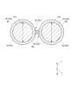
図3は、波長変換素子51を励起光の入射側から見た平面図である。図4は、波長変換素子51の断面を模式的に示す図である。
波長変換素子51は、励起光の波長とは異なる波長を有する光である蛍光を、励起光の入射側に出射する反射型の波長変換素子である。波長変換素子51は、図3及び図4に示すように、基板52、放熱シート53、蛍光体層54及び反射防止層55を有する。なお、波長変換素子51は、後述する製造方法によって製造される。
なお、以降の説明及び図においては、波長変換素子51に入射される青色光L1sを、波長変換素子51に含まれる蛍光体粒子を励起させる励起光と記載する。また、波長変換素子51に対する励起光の入射方向を+Z方向とし、+Z方向とは反対方向を-Z方向とする。
[Configuration of Wavelength Conversion Element]
FIG. 3 is a plan view of the
The
In the following description and drawings, the blue light L1s incident on the
[基板の構成]
基板52は、放熱シート53、蛍光体層54及び反射防止層55を保持する保持部材である他、蛍光体層54から伝達される熱を放熱する放熱部材でもある。基板52は、図3に示すように、例えばアルミナや酸化亜鉛の少なくともいずれかを含む金属材料によって、-Z方向から見て円板状に形成されている。基板52は、回転部RTによって回転軸Rxを中心として、放熱シート53、蛍光体層54及び反射防止層55とともに回転される。
基板52は、図4に示すように、-Z方向の面である第1面521と、+Z方向の面である第2面522と、を有する。
第1面521は、蛍光体層54と対向する対向面である。
第2面522は、第1面521とは反対側の面である。第2面522には、放熱シート53が接着されており、蛍光体層54で発生した熱は基板52を介して、放熱シート53に伝えられ、伝えられた熱は放熱シート53全体に伝えられる。放熱シート53は、周囲の気体との接触面積を拡大することによって、基板52に伝達された熱の放熱効率を高めている。放熱シート53は、例えばアルミニウムやグラファイト等により構成される。
基板52は、サブミクロンオーダーのアルミナ紛体を低温で焼成して内部に微小な気孔を体積比で20%程度含んだ焼結体であり、蛍光体層54から入射される光を、蛍光体層54側に反射する。
[Substrate configuration]
The
As shown in FIG. 4, the
The
The
The
[蛍光体層の構成]
蛍光体層54は、基板52に対して励起光の入射側である-Z方向に設けられている。蛍光体層54は、入射される励起光を蛍光に変換して出射する。換言すると、蛍光体層54は、入射される励起光を波長変換して、励起光の波長より長い波長を有する光である蛍光を生成して出射する。蛍光体層54は、図3に示すように、-Z方向から見て、波長変換素子51の回転軸Rxを中心とする円環状に形成されている。
[Structure of Phosphor Layer]
The
蛍光体層54は、図4に示すように、-Z方向の面である第1面541と、+Z方向の面であり、第1面541とは反対側の面である第2面542と、を有する。
第1面541は、励起光が入射される入射面であり、蛍光が出射される出射面である。
第2面542は、基板52と対向する対向面である。
As shown in FIG. 4, the
The
The
図5は、蛍光体層54及び反射防止層55の一部を拡大して示す模式図である。換言すると、図5は、蛍光体層54を構成する複数の蛍光体粒子P1及びバインダーBNと、反射防止層55とを模式的に示す断面図である。
蛍光体層54は、図5に示すように、複数の蛍光体粒子PRと、ガラスを含有するバインダーBNとを含み、複数の蛍光体粒子PRがバインダーBNによって互いに結合された構成を有する。具体的に、隣り合う2つの蛍光体粒子PRは、それぞれの表面の一部に接合されるバインダーBNによって互いに結合されている。
FIG. 5 is a schematic diagram showing an enlarged part of the
As shown in FIG. 5, the
蛍光体粒子PRは、蛍光体材料と、発光中心となる賦活剤とを含有する粒子である。賦活剤としては、例えばCe、Eu、Pr、Cr、Gd及びGaが挙げられる。蛍光体材料としては、YAG蛍光体材料を採用できる。しかしながら、これに限らず、蛍光体材料は、YAG蛍光体材料に代えて、YAG蛍光体におけるYがLu、Gd又はGaで置換された蛍光体材料を採用してもよく、KSF蛍光体材料、又は、SCASN蛍光体材料等を採用してもよい。更に、蛍光体材料は、複数の蛍光体材料の混合物であってもよい。
バインダーBNは、複数の蛍光体粒子PRのうち、隣り合う蛍光体粒子PRのそれぞれの表面の一部に接合して、隣り合う蛍光体粒子PRを結合させる。本実施形態では、バインダーBNとして、ホウケイ酸ガラスが用いられているが、リン酸塩系ガラスであってもよい。
なお、蛍光体層54の内部には、微小な空隙SPが設けられている。このような空隙SPが含まれていることによって、蛍光体層54内部での蛍光の広がりを抑え、蛍光体層54からの蛍光を小さい範囲で取り出すことによって、光学系の集光効率が高められる。
The phosphor particles PR are particles containing a phosphor material and an activator serving as a luminescence center. Activators include, for example, Ce, Eu, Pr, Cr, Gd and Ga. A YAG phosphor material can be used as the phosphor material. However, the phosphor material is not limited to this, and instead of the YAG phosphor material, a phosphor material in which Y in the YAG phosphor is replaced with Lu, Gd or Ga may be adopted, KSF phosphor material, Alternatively, a SCASN phosphor material or the like may be employed. Further, the phosphor material may be a mixture of multiple phosphor materials.
The binder BN joins to a part of the surface of each of the adjacent phosphor particles PR among the plurality of phosphor particles PR to bind the adjacent phosphor particles PR. In this embodiment, borosilicate glass is used as the binder BN, but phosphate glass may be used.
A minute gap SP is provided inside the
反射防止層55は、図4に示すように、少なくとも蛍光体層54において励起光が入射される入射面である第1面541に設けられており、例えば単層又は多層の誘電体膜によって構成される。すなわち、反射防止層55は、蛍光体層54に対する励起光の入射側に設けられている。反射防止層55は、波長変換素子51に入射される励起光が第1面541にて反射されることを抑制することによって、励起光を蛍光体層54に入射させやすくする。
このような反射防止層55は、蛍光体層54に蒸着等によって形成される。このため、図5に示すように、複数の蛍光体粒子PRのうち、蛍光体層54において-Z方向に位置して第1面541を形成する複数の蛍光体粒子PRAと、複数の蛍光体粒子PRAを結合させるバインダーBNとを、-Z方向にて覆うように形成される。
本実施形態では、反射防止層55は、蛍光体層54の第1面541にのみ形成されている。しかしながら、これに限らず、反射防止層55は、第1面541に加えて、例えば蛍光体層54の内周面及び外周面の少なくともいずれかに形成されていてもよい。
As shown in FIG. 4, the
Such an
In this embodiment, the
[蛍光体粒子における結合部の面積と光学系での明るさとの関係]
図6は、バインダーBNによる蛍光体粒子PRの結合状態を示す模式図である。換言すると、図6は、隣り合う蛍光体粒子PR(PR1,PR2)がバインダーBNによって結合された状態を示す模式図である。
図6に示すように、蛍光体粒子PRにおいてバインダーBNが接合される部位を結合部B1とすると、本実施形態では、蛍光体層54から出射された蛍光を含む照明光が入射される光学系である光学装置30を透過する光の明るさを高めるために、結合部B1の面積は、蛍光体粒子PRの表面積の10%以下の値に設定されている。詳述すると、結合部B1の面積は、蛍光体粒子PRの表面積の3%以上、5%以下の範囲内の値に設定されている。これは、以下の実験結果によるものである。
[Relationship between the area of the bonding part in the phosphor particles and the brightness in the optical system]
FIG. 6 is a schematic diagram showing how the phosphor particles PR are bound by the binder BN. In other words, FIG. 6 is a schematic diagram showing a state in which adjacent phosphor particles PR (PR1, PR2) are bound together by binder BN.
As shown in FIG. 6, if the site where the binder BN is bonded in the phosphor particles PR is a bonding portion B1, in the present embodiment, an optical system in which the illumination light containing the fluorescence emitted from the
図7は、蛍光体粒子PRの表面積に占める結合部B1の面積の割合に対する光学装置30における光学系での明るさ及び光の広がりを示すグラフである。
発明者は、蛍光体粒子PRの表面積に対する結合部B1の面積の割合を変化させ、蛍光体層54から出射される光の広がり、及び、光学装置30における光学系での明るさを測定する実験を行った。なお、ここでいう光学系での明るさは、光変調装置343に集光可能な光量を示している。また、光の広がりは、蛍光体層54の第1面541において、励起光の入射領域の面積に対する蛍光の出射領域の面積の割合である。以下の説明では、蛍光体粒子PRの表面積に対する結合部B1の面積の割合を、面積割合と略す。
蛍光体層54から出射される光の広がりは、図7に一点鎖線によって示されるように、面積割合が大きいほど大きくなった。すなわち、蛍光体層54から出射される光の広がりは、結合部B1の面積が大きいほど大きくなった。
FIG. 7 is a graph showing the brightness and spread of light in the optical system of the
The inventor conducted an experiment to measure the spread of light emitted from the
The spread of the light emitted from the
光学系での明るさは、図7に実線によって示されるように、面積割合が小さいほど高くなるわけではなく、光学系での明るさには、最大値(最高値)があることが分かった。
詳述すると、面積割合が10%以下の範囲では、光学系での明るさは、面積割合が大きくなるに従って高くなった後に低くなった。そして、光学系での明るさの最大値は、面積割合が3%以上、5%以下の範囲内にあるときに示されることが分かった。
一方、面積割合が10%を超える範囲では、光学系での明るさは、面積割合が0%であるときより低くなり、面積割合が大きいほど低くなった。
すなわち、光学系での明るさは、面積割合が10%以下であるときに0%であるときよりも高くなり、面積割合が3%以上、5%以下の範囲内にあるときに最大となることが分かった。
As shown by the solid line in FIG. 7, the brightness in the optical system does not increase as the area ratio decreases, and it was found that the brightness in the optical system has a maximum value (highest value). .
More specifically, when the area ratio is 10% or less, the brightness in the optical system increases and then decreases as the area ratio increases. It was also found that the maximum value of brightness in the optical system is exhibited when the area ratio is in the range of 3% or more and 5% or less.
On the other hand, when the area ratio exceeded 10%, the brightness in the optical system was lower than when the area ratio was 0%, and decreased as the area ratio increased.
That is, the brightness in the optical system is higher when the area ratio is 10% or less than when it is 0%, and becomes maximum when the area ratio is in the range of 3% or more and 5% or less. I found out.
このように、光学系での明るさが高くなるときの面積割合の範囲が存在することは、以下の理由によると考えられる。
蛍光体粒子PRの屈折率は、約1.8である。これに対し、バインダーBNを構成するホウケイ酸ガラスの屈折率は、約1.5である。
このことから、蛍光体粒子PRの内部にて生成されて結合部B1に入射された蛍光は、結合部B1からバインダーBNを伝わって、隣り合う蛍光体粒子PR内に進行する。
一方、蛍光体層54の内部には空隙SPが設けられていることから、蛍光体粒子PRの外面において結合部B1以外の領域は、空気と接している。このため、フレネルの式に従い、蛍光体粒子PRの内部にて生成されて、蛍光体粒子PRの外面において結合部B1以外の領域に入射された蛍光は、屈折して大部分が蛍光体粒子PRの外部に出射されて一部が内部に反射するか、或いは、蛍光体粒子PR内部に全反射される。
The reason why there is such a range of area ratios when the brightness in the optical system is high is considered to be as follows.
The refractive index of the phosphor particles PR is approximately 1.8. In contrast, the borosilicate glass that constitutes the binder BN has a refractive index of about 1.5.
Therefore, the fluorescence generated inside the phosphor particle PR and incident on the joint portion B1 travels from the joint portion B1 through the binder BN and advances into the adjacent phosphor particle PR.
On the other hand, since the space SP is provided inside the
面積割合が大きい場合、結合部B1に入射される蛍光の光量が多くなる。すなわち、面積割合が大きい場合、結合部B1を介してバインダーBNを伝わる蛍光の光量が多くなる。この場合、蛍光体粒子PRの屈折率とバインダーBNの屈折率との差が小さく、蛍光体粒子PRとバインダーBNとの界面での屈折が小さいため、蛍光が周辺の蛍光体粒子PRに広がりやすくなる。このため、蛍光体層54の第1面541から外部に、大きな広がりの光源として蛍光が出ていく。これにより、光学系である光学装置30の光変調装置343に、蛍光体層54から出射された蛍光を集光しにくくなる。すなわち、この場合には、光学系での明るさが低くなる。
When the area ratio is large, the amount of fluorescent light incident on the coupling portion B1 increases. That is, when the area ratio is large, the amount of fluorescence light transmitted through the binder BN via the joint portion B1 increases. In this case, since the difference between the refractive index of the phosphor particles PR and the refractive index of the binder BN is small and the refraction at the interface between the phosphor particles PR and the binder BN is small, fluorescence tends to spread to the surrounding phosphor particles PR. Become. Therefore, fluorescence is emitted from the
面積割合が小さい場合、蛍光体粒子PRの内部にて生成された蛍光は、蛍光体粒子PRの外面において結合部B1以外の領域、すなわち、空気との界面に入射されやすくなる。このため、蛍光体粒子PRと空気との界面にて屈折されて蛍光体粒子PRから出射される蛍光の光量、及び、全反射される蛍光の光量が多くなることから、周辺の広範囲の蛍光体粒子PRに蛍光が広がることが抑制され、蛍光体層54の第1面541から外部に、小さな広がりの光源として蛍光が出ていく。このような蛍光は、光変調装置343に集光しやすい。すなわち、この場合には、光学系での明るさが高くなる。
When the area ratio is small, the fluorescence generated inside the phosphor particles PR is likely to enter the region other than the bonding portion B1 on the outer surface of the phosphor particles PR, that is, the interface with the air. For this reason, the amount of fluorescent light emitted from the fluorescent particles PR after being refracted at the interface between the fluorescent particles PR and the air, and the amount of fluorescent light totally reflected are increased. Spreading of the fluorescence to the particles PR is suppressed, and the fluorescence is emitted from the
一方、面積割合が、例えば1%以下の値のような非常に小さい値である場合、蛍光が蛍光体粒子PRの内部に閉じ込められやすくなる。この場合には、空隙SPとの界面での蛍光の反射が繰り返されやすくなって、蛍光の光路長が大きくなる。このように、蛍光体粒子PR内を蛍光が何度も通ることで、自己吸収が生じやすくなる。自己吸収とは、蛍光体の発光波長が蛍光体の吸収波長と部分的に重なっているために、蛍光体が蛍光を吸収して発熱する現象である。このような自己吸収が生じると、蛍光体層54から出射される蛍光の光量が減少し、ひいては、光学系での明るさが低くなる。
On the other hand, when the area ratio is a very small value such as 1% or less, fluorescence tends to be confined inside the phosphor particles PR. In this case, fluorescence is likely to be repeatedly reflected at the interface with the void SP, and the optical path length of the fluorescence is increased. In this way, self-absorption tends to occur due to fluorescence passing through the interior of the phosphor particles PR many times. Self-absorption is a phenomenon in which the phosphor absorbs fluorescence and generates heat because the emission wavelength of the phosphor partially overlaps the absorption wavelength of the phosphor. When such self-absorption occurs, the amount of fluorescent light emitted from the
他方、蛍光体粒子PRにおける空気との界面での反射及び屈折の頻度が高くなると、蛍光体層54の外部から照射される励起光が、蛍光体粒子PRの表面、或いは、蛍光体粒子PRの内部にて反射されやすくなる。蛍光に変換されることなく、蛍光体層54の外部に放射される励起光の光量が大きくなる。すなわち、励起光の後方散乱(バックスキャッタ)が生じやすくなる。この場合には、蛍光に変換される励起光の光量が減少することによって、蛍光体層54から出射される蛍光の光量が減少し、ひいては、光学系での明るさが低くなり得る。
On the other hand, when the frequency of reflection and refraction of the phosphor particles PR at the interface with the air increases, the excitation light irradiated from the outside of the
このような考察から、光学系での明るさを高くするためには、面積割合は、10%以下の値であることが好ましく、3%以上、5%以下の値であることがより好ましいことが分かった。 From these considerations, in order to increase the brightness in the optical system, the area ratio is preferably a value of 10% or less, and more preferably a value of 3% or more and 5% or less. I found out.
[蛍光体粒子におけるバインダーとの結合部の大きさ]
本実施形態では、蛍光体粒子PRの表面積に対する結合部B1の面積の割合を10%以下にするために、結合部B1の大きさが以下の大きさになるように、蛍光体層54を作製している。なお、以下の説明では、図6に示すように、複数の蛍光体粒子PRのうち、バインダーBNによって結合され、かつ、互いに隣り合う蛍光体粒子を蛍光体粒子PR1,PR2とする。また、蛍光体粒子PR1におけるバインダーBNとの結合部B1を、結合部B11とし、蛍光体粒子PR2におけるバインダーBNとの結合部B1を結合部B12とする。更に、蛍光体粒子PR1,PR2の各中心C1,C2を結ぶ仮想線VLに直交し、かつ、互いに直交する二軸をX軸及びY軸とする。
[Size of bonding portion with binder in phosphor particles]
In the present embodiment, the
本実施形態では、結合部B11のY軸における寸法は、蛍光体粒子PR1の直径D11の1/4以下とされ、図示を省略するが、結合部B11のX軸における寸法は、蛍光体粒子PR1の直径D11の1/4以下とされている。換言すると、結合部B11のY軸における寸法は、蛍光体粒子PR1のY軸における大きさの1/4以下とされ、図示を省略するが、結合部B11のX軸における寸法は、蛍光体粒子PR1のX軸における大きさの1/4以下とされている。
同様に、結合部B12のY軸における寸法は、蛍光体粒子PR2の直径D12の1/4以下とされ、図示を省略するが、結合部B12のX軸における寸法は、蛍光体粒子PR2の直径D12の1/4以下とされている。換言すると、結合部B12のY軸における寸法は、蛍光体粒子PR2のY軸における大きさの1/4以下とされ、図示を省略するが、結合部B12のX軸における寸法は、蛍光体粒子PR2のX軸における大きさの1/4以下とされている。
更に、バインダーBNの厚み、すなわち、仮想線VLに沿うバインダーBNの寸法は、蛍光体粒子PRの直径の1/10以下とされている。
このように、結合部B1の寸法が上記の大きさであることにより、上記割合が10%以下の値となり、光学系での明るさを高くすることができる。
In the present embodiment, the dimension of the joint B11 along the Y axis is set to 1/4 or less of the diameter D11 of the phosphor particle PR1. 1/4 or less of the diameter D11. In other words, the dimension of the joint B11 along the Y axis is 1/4 or less of the size of the phosphor particle PR1 along the Y axis. It is set to 1/4 or less of the size of PR1 on the X axis.
Similarly, the dimension of the joint B12 along the Y axis is set to 1/4 or less of the diameter D12 of the phosphor particle PR2. It is said to be 1/4 or less of D12. In other words, the dimension of the joint B12 along the Y axis is 1/4 or less of the size of the phosphor particle PR2 along the Y axis. It is set to 1/4 or less of the size of PR2 on the X axis.
Furthermore, the thickness of the binder BN, that is, the dimension of the binder BN along the virtual line VL is set to 1/10 or less of the diameter of the phosphor particles PR.
In this way, by setting the size of the coupling portion B1 to the above size, the above ratio becomes a value of 10% or less, and the brightness in the optical system can be increased.
[計算による結合部の大きさ]
光学系での明るさを高める上記面積割合は、蛍光体粒子PRの直径に基づく計算結果からも裏付けられる。
蛍光体層54に含まれる蛍光体粒子PRを球状と仮定した場合、半径Rの蛍光体粒子PRの表面積は、4π・R2である。
一方、粒径が略揃った球形の蛍光体粒子PRが密に配列されている場合、単位体積当たりの蛍光体粒子PRの充填率は、一般的に60~75%である。この場合、1つの蛍光体粒子PRが接する他の蛍光体粒子PRの数は、8~12である。
[Calculated joint size]
The area ratio that increases the brightness in the optical system is also supported by the calculation results based on the diameter of the phosphor particles PR.
Assuming that the phosphor particles PR contained in the
On the other hand, when the spherical phosphor particles PR having substantially uniform particle diameters are densely arranged, the filling rate of the phosphor particles PR per unit volume is generally 60 to 75%. In this case, the number of other phosphor particles PR with which one phosphor particle PR is in contact is 8-12.
1つの蛍光体粒子PRが接する他の蛍光体粒子PRの数を8と仮定し、バインダーBNを、厚みtで半径rの円柱と仮定した場合、結合部B1の総面積は、8π・r2である。なお、バインダーBNの厚みは、図6に示した仮想線VLに沿う寸法である。
これらのことから、上記面積割合は、8π・r2/(4π・R2)となる。すなわち、上記面積割合は、2r2/R2となる。
Assuming that the number of other phosphor particles PR that one phosphor particle PR is in contact with is 8, and the binder BN is assumed to be a cylinder having a thickness t and a radius r, the total area of the bonding portion B1 is 8π·r 2 is. The thickness of the binder BN is a dimension along the imaginary line VL shown in FIG.
From these facts, the area ratio is 8π·r 2 /(4π·R 2 ). That is, the area ratio is 2r 2 /R 2 .
蛍光体粒子PRの半径Rを12μmと仮定し、蛍光体粒子PRの表面積に占める結合部B1の割合を、上記した実験結果から5%(=0.05)と仮定した場合、結合部B1の半径rは、略1.89μmとなる。すなわち、蛍光体粒子P1における結合部B1の形状を円とした場合の結合部B1の半径rは、略2μmとなり、結合部B1の直径は、略4μmとなる。また、1つの蛍光体粒子PRが接する他の蛍光体粒子PRの数を12と仮定すれば、結合部B1の半径rは、略3μmとなり、結合部BPの直径は、略6μmとなる。よって、結合部B1の半径rは、略2~3μmであり、結合部B1の直径は、略4~6μmである。
このような計算によって求められる結合部B1の直径は、上記仮定に基づく蛍光体粒子PRの直径24μmの1/4以下の値である。換言すると、結合部B1のX軸及びY軸における寸法は、蛍光体粒子PRの直径の1/4以下の値である。
以上のように、蛍光体粒子PRの直径に対して結合部B1の寸法を上記した大きさにすることによって、上記面積割合を10%以下にすることができ、ひいては、光学系での明るさを高くできる。
このような結合部B1の大きさは、詳しくは後述するが、蛍光体層54を製造する際の温度を調整することによって実現できる。これについては、波長変換素子51の製造方法にて説明する。
Assuming that the radius R of the phosphor particles PR is 12 μm, and assuming that the ratio of the bonding portions B1 to the surface area of the phosphor particles PR is 5% (=0.05) from the above experimental results, the bonding portions B1 The radius r is approximately 1.89 μm. That is, when the shape of the joint B1 in the phosphor particle P1 is circular, the radius r of the joint B1 is approximately 2 μm, and the diameter of the joint B1 is approximately 4 μm. Also, assuming that the number of other phosphor particles PR with which one phosphor particle PR is in contact is 12, the radius r of the joint B1 is approximately 3 μm, and the diameter of the joint BP is approximately 6 μm. Therefore, the radius r of the connecting portion B1 is approximately 2 to 3 μm, and the diameter of the connecting portion B1 is approximately 4 to 6 μm.
The diameter of the joint B1 obtained by such calculation is a value of 1/4 or less of the
As described above, by setting the size of the bonding portion B1 to the diameter of the phosphor particle PR as described above, the area ratio can be made 10% or less. can be raised.
Such a size of the joint portion B1 can be realized by adjusting the temperature when manufacturing the
[蛍光体層におけるガラス含有率]
図8は、蛍光体層54のガラス含有率と光学系効率との関係を示すグラフである。
なお、ガラス含有率は、蛍光体層54においてバインダーBNの体積割合(vol%)により表される。具体的に、ガラス含有率は「100*ガラスの体積/(ガラスの体積+蛍光体粒子の体積)」であり、空隙SPの体積は含まれていない。
すなわち、ここでいうガラス含有率は、作製後の波長変換素子51の実測値ではなく、後述する波長変換素子51の製造工程におけるペースト調製工程S1及び蛍光体混合工程S2(図14参照)でのバインダーBN及び蛍光体粒子PRの投入量の体積割合に基づく値である。
[Glass Content in Phosphor Layer]
FIG. 8 is a graph showing the relationship between the glass content of the
Note that the glass content is represented by the volume ratio (vol %) of the binder BN in the
That is, the glass content rate referred to here is not the measured value of the
一方、光学系効率は、「蛍光体層54から出射されて光学系である光学装置30を透過した後、投射光学装置36から出射した光の光量/蛍光体層54に照射された励起光の光量」である。このため、光学系効率は、「蛍光体層54から出射されて光学装置30に入射した光の光量/蛍光体層54に照射された励起光の光量」ではなく、「蛍光体層54から出射された光の光量/蛍光体層54に照射された励起光の光量」により示される波長変換効率でもない。
すなわち、光学系効率は、エテンデューを含んだ効率であり、プロジェクター1の光学装置30における光利用効率と言い換えることができる。
On the other hand, the optical system efficiency is defined as “the amount of light emitted from the projection
That is, the optical system efficiency is an efficiency including etendue, and can be rephrased as a light utilization efficiency in the
図8に示されるように、本実施形態に係る蛍光体層54において、ガラス含有率が0vol%より大きく、10vol%以下の範囲内では、ガラス含有率が0vol%であるときに比べて、光学系効率が高くなっている。そして、ガラス含有率が10vol%であると、光学系効率は、ガラス含有率が0vol%であるときと略同じ値となる。
ガラス含有率が10vol%を超えると、ガラス含有率が0vol%であるときに比べて、光学系効率が低下する。これは、上記のように、蛍光体粒子PRとバインダーBNとの界面にて、蛍光が反射及び屈折をすることによる損失は低下する一方で、蛍光が蛍光体層54中を広がり、蛍光が蛍光体層54から出射される際の光の広がりが大きくなり、光学系である光学装置30にて利用できる光量が低下して、測定値の差として表れたものと考えられる。また、0~10%との間でピークを示すのは、バインダーBNが極端に少ないと、蛍光体粒子PRと空隙SP(空気)との界面にて、励起光が何回も反射及び屈折を繰り返すことによって、当該励起光が蛍光体を励起する前に、蛍光体層54から放出されてしまうことによるものと考えられる。
As shown in FIG. 8, in the
If the glass content exceeds 10 vol%, the optical system efficiency will be lower than when the glass content is 0 vol%. This is because, as described above, the loss due to the reflection and refraction of the fluorescence at the interface between the phosphor particles PR and the binder BN is reduced, while the fluorescence spreads in the
図9は、ガラス含有率が30vol%であり、蛍光体層の焼成温度が1000℃である蛍光体層をSEM(Scanning Electron Microscope:走査型電子顕微鏡)により観察した際の画像である。以下、SEMによって観察される画像をSEM画像と略す。
図10は、ガラス含有率が20vol%であり、蛍光体層の焼成温度が1000℃である蛍光体層のSEM画像である。図11は、ガラス含有率が10vol%であり、蛍光体層の焼成温度が1000℃である蛍光体層のSEM画像である。図12は、ガラス含有率が5vol%であり、蛍光体層の焼成温度が1000℃である蛍光体層のSEM画像である。図13は、ガラス含有率が3vol%であり、蛍光体層の焼成温度が1000℃である蛍光体層のSEM画像である。
FIG. 9 is an image of a phosphor layer having a glass content of 30 vol % and a phosphor layer firing temperature of 1000° C. when observed with a SEM (Scanning Electron Microscope). An image observed by an SEM is abbreviated as an SEM image hereinafter.
FIG. 10 is an SEM image of a phosphor layer having a glass content of 20 vol % and a firing temperature of the phosphor layer of 1000°C. FIG. 11 is an SEM image of a phosphor layer having a glass content of 10 vol % and a firing temperature of the phosphor layer of 1000°C. FIG. 12 is an SEM image of a phosphor layer having a glass content of 5 vol % and a firing temperature of the phosphor layer of 1000°C. FIG. 13 is an SEM image of a phosphor layer having a glass content of 3 vol % and a firing temperature of the phosphor layer of 1000°C.
ガラス含有率が30vol%及び20vol%である蛍光体層では、図9及び図10に示すように、全ての蛍光体粒子PRの表面がバインダーBNによって略完全に覆われている。特に、図9に示されるガラス含有率が30vol%である蛍光体層では、各蛍光体粒子PRはバインダーBNの中に埋没されている。このように蛍光体粒子PRが、ホウケイ酸ガラスであるバインダーBNによって覆われると、上記のように、蛍光体粒子PRにて生成された蛍光がバインダーBNを伝播しやすくなり、蛍光体層から出射される光の広がりが大きくなって、光学系効率が低下する。 In the phosphor layers with glass contents of 30 vol % and 20 vol %, the surfaces of all the phosphor particles PR are substantially completely covered with the binder BN, as shown in FIGS. 9 and 10 . In particular, in the phosphor layer having a glass content of 30 vol % shown in FIG. 9, each phosphor particle PR is embedded in the binder BN. When the phosphor particles PR are covered with the binder BN, which is borosilicate glass, as described above, the fluorescence generated by the phosphor particles PR easily propagates through the binder BN, and is emitted from the phosphor layer. The spread of the emitted light is increased and the efficiency of the optical system is reduced.
これに対し、ガラス含有率が10vol%、5vol%及び3vol%である蛍光体層では、図11~図13に示すように、バインダーBNは、隣り合う蛍光体粒子PRの間に設けられ、蛍光体粒子PRは、バインダーBNによって完全には覆われていない。特に、ガラス含有率が5vol%及び3vol%である蛍光体層では、図12及び図13に示すように、バインダーBNは、隣り合う蛍光体粒子PRの間にのみ設けられ、蛍光体粒子PRの表面は、ほぼ露出されている。
このように、バインダーBNによって、隣り合う蛍光体粒子PRが表面の一部にて結合され、他の部分が露出されていることにより、蛍光体層から出射される光の広がりが小さくなり、光学系効率が高められる。
従って、ガラス含有率は、0vol%より大きく、10vol%以下の範囲内の値であることにより、ガラス含有率が0vol%のとき、及び、ガラス含有率が10vol%より大きい場合に比べて、光学系効率を高められる蛍光体層を構成できる。
On the other hand, in the phosphor layers with glass contents of 10 vol%, 5 vol%, and 3 vol%, the binder BN is provided between adjacent phosphor particles PR, as shown in FIGS. The body particles PR are not completely covered by the binder BN. In particular, in phosphor layers with a glass content of 5 vol % and 3 vol %, as shown in FIGS. 12 and 13, the binder BN is provided only between the adjacent phosphor particles PR. The surface is mostly exposed.
In this way, the binder BN binds the adjacent phosphor particles PR at a part of the surface and exposes the other part. System efficiency is enhanced.
Therefore, when the glass content is a value in the range of greater than 0 vol% and 10 vol% or less, the optical A phosphor layer capable of increasing system efficiency can be constructed.
[波長変換素子の製造方法]
図14は、波長変換素子51の製造方法を示すフローチャートである。
上記した蛍光体層54を含む波長変換素子51の製造方法について、説明する。
波長変換素子51の製造方法は、図14に示すように、順に実施されるペースト調製工程S1、蛍光体混合工程S2、印刷版作成工程S3、塗布工程S4、乾燥工程S5、焼成工程S6、冷却工程S7及び層形成工程S8を含む。すなわち、以下に示す波長変換素子51の製造方法は、本発明の製造方法を含む。
[Method for producing wavelength conversion element]
FIG. 14 is a flow chart showing a method of manufacturing the
A method of manufacturing the
As shown in FIG. 14, the method of manufacturing the
ペースト調製工程S1及び蛍光体混合工程S2は、調製工程に相当する。
ペースト調製工程S1は、焼成後にバインダーBNとなるバインダー構成物と、エチルセルロース等の樹脂と、バインダー構成物及び樹脂を溶かす溶剤とを混合して、ガラスペーストを調製する工程である。なお、樹脂は、ペーストに粘性を付与するためのものである。また、バインダー構成物としては、例えばシリカが60%以上含まれるホウケイ酸ガラスを直径1μm以下に砕いたものが挙げられる。
蛍光体混合工程S2は、調製されたガラスペースト中に蛍光体粒子PRを混合した混合ペーストを調製する工程である。蛍光体粒子PRとバインダー構成物であるホウケイ酸ガラスとの割合は、体積比で98:2~92:8の範囲内の割合とする。なお、当該範囲は、98:2及び92:8を含む範囲である。より好ましくは、蛍光体粒子PRとホウケイ酸ガラスとの割合は、体積比で97:3~95:5の範囲内の割合とする。当該範囲は、97:3及び95:5を含む範囲である。このように蛍光体粒子PRとホウケイ酸ガラスとの割合を調整することによって、ガラス含有率を上記範囲内の値に設定できる。
The paste preparation step S1 and the phosphor mixing step S2 correspond to preparation steps.
The paste preparation step S1 is a step of preparing a glass paste by mixing a binder component that will become a binder BN after firing, a resin such as ethyl cellulose, and a solvent that dissolves the binder component and the resin. Incidentally, the resin is for imparting viscosity to the paste. Further, as the binder constituent, for example, borosilicate glass containing 60% or more of silica is crushed to a diameter of 1 μm or less.
The phosphor mixing step S2 is a step of preparing a mixed paste by mixing phosphor particles PR into the prepared glass paste. The volume ratio of the phosphor particles PR to the borosilicate glass, which is the binder component, is in the range of 98:2 to 92:8. The range includes 98:2 and 92:8. More preferably, the volume ratio of the phosphor particles PR to the borosilicate glass is in the range of 97:3 to 95:5. The range is inclusive of 97:3 and 95:5. By adjusting the ratio of the phosphor particles PR and the borosilicate glass in this manner, the glass content can be set to a value within the above range.
印刷版作成工程S3は、円形の形状に印刷が抜けるように印刷版を作製する。
塗布工程S4は、作製された印刷版を用いて、円板形状の反射板上に、蛍光体混合工程S2にて調製された混合ペーストを厚さ80μmで印刷塗布する。反射板は、内部に反射用の微小気孔が設けられた基板52である。
乾燥工程S5では、塗布された混合ペーストを100℃程度で短時間乾燥させる。
In the printing plate making step S3, a printing plate is made so that the print is drawn in a circular shape.
In the coating step S4, the prepared printing plate is used to print and apply the mixed paste prepared in the phosphor mixing step S2 to a thickness of 80 μm on the disk-shaped reflector. The reflector is a
In the drying step S5, the applied mixed paste is dried at about 100° C. for a short time.
焼成工程S6では、乾燥された混合ペーストを、焼成炉にて1000℃まで10℃/分の割合で昇温しつつ、短時間焼成する。焼成工程S6にて混合ペーストを焼成すると、混合ペーストに含まれていた樹脂及び溶剤の略全てが蒸発する。なお、焼成工程S6での焼成温度については、後に詳述する。
冷却工程S7では、焼成された混合ペーストを冷却する。
In the firing step S6, the dried mixed paste is fired in a firing furnace for a short time while raising the temperature to 1000°C at a rate of 10°C/min. When the mixed paste is fired in the firing step S6, substantially all of the resin and solvent contained in the mixed paste evaporate. The firing temperature in the firing step S6 will be detailed later.
In the cooling step S7, the fired mixed paste is cooled.
層形成工程S8では、冷却工程S7にて冷却された混合ペーストである蛍光体層54に反射防止層55を形成する。具体的に、層形成工程S8では、蛍光体層54において基板52とは反対側の面であり、励起光が入射される第1面541に蒸着等によって誘電体膜を形成し、これにより、第1面541に反射防止層55を形成する。あるいは、蛍光体層54の上部の曲面や蛍光体層54の内部の表面につける方法として、CVD(Chemical Vapor Deposition)やALD(Atomic Layer Deposition)を用いることができる。これにより蛍光体層54の内部まで誘電体物質である、SiO2やTiO2の気体を蛍光体層54の内部に行き届かせて成膜することが可能である。それにより、励起光が蛍光体層54の内部に至っても、蛍光体粒子PRの表面で反射されるのを防ぎ、より多くの励起光を蛍光へと変換することができる。
以上の各工程S1~S8を含む製造方法によって、上記面積割合及びガラス含有率が0%より大きく、10%以下である蛍光体層54を有する波長変換素子51が製造される。
In the layer forming step S8, an
By the manufacturing method including the steps S1 to S8 described above, the
[焼成工程での焼成温度とガラスの粘度との関係]
図15は、焼成温度とガラスの粘度との関係を示すグラフである。
ガラスの粘度は、図15に示すように、温度が高くなるに従って低下し、ガラスの粘性による力は、粘度が小さくなるに従って弱くなる。そして、ガラスが自重で顕著に軟化変形し始める温度であり、粘度が約107.6dPa・sとなる温度である軟化点を700℃とすると、上記焼成工程S6の焼成温度を軟化点+100℃である800℃以上にすることにより、ガラスの粘度は、106dPa・s(=106P)以下となる。
[Relationship between firing temperature and viscosity of glass in firing process]
FIG. 15 is a graph showing the relationship between firing temperature and glass viscosity.
As shown in FIG. 15, the viscosity of the glass decreases as the temperature increases, and the force due to the viscosity of the glass decreases as the viscosity decreases. Assuming that the softening point, which is the temperature at which the glass begins to be significantly softened and deformed by its own weight and the temperature at which the viscosity becomes about 10 7.6 dPa·s, is 700° C., the firing temperature in the firing step S6 is set to the softening point +100. When the temperature is 800° C. or higher, the viscosity of the glass becomes 10 6 dPa·s (=10 6 P) or lower.
以下、ガラス含有率が5vol%である混合ペーストを各焼成温度で焼成して作製される蛍光体層のSEM画像を以下に示す。
すなわち、図16は、ガラス含有率が5vol%であり、750℃で焼成されて作製された蛍光体層を示すSEM画像である。図17は、ガラス含有率が5vol%であり、800℃で焼成されて作製された蛍光体層を示すSEM画像である。図18は、ガラス含有率が5vol%であり、850℃で焼成されて作製された蛍光体層を示すSEM画像である。図19は、ガラス含有率が5vol%であり、900℃で焼成されて作製された蛍光体層を示すSEM画像である。図20は、ガラス含有率が5vol%であり、950℃で焼成されて作製された蛍光体層を示すSEM画像である。
なお、上記のように、図12には、ガラス含有率が5vol%であり、1000℃で焼成されて作製された蛍光体層のSEM画像が示されている。
SEM images of phosphor layers produced by firing a mixed paste having a glass content of 5 vol % at each firing temperature are shown below.
That is, FIG. 16 is an SEM image showing a phosphor layer having a glass content of 5 vol % and being fired at 750° C. FIG. FIG. 17 is an SEM image showing a phosphor layer fabricated with a glass content of 5 vol % and fired at 800°C. FIG. 18 is an SEM image showing a phosphor layer fabricated with a glass content of 5 vol % and fired at 850.degree. FIG. 19 is an SEM image showing a phosphor layer fabricated with a glass content of 5 vol % and fired at 900°C. FIG. 20 is an SEM image showing a phosphor layer fabricated with a glass content of 5 vol % and fired at 950°C.
As described above, FIG. 12 shows an SEM image of a phosphor layer having a glass content of 5 vol % and being fired at 1000.degree.
ガラスの軟化点に近い750℃にて焼成された蛍光体層では、図16に示すように、蛍光体粒子PRの直径に対する結合部B1の大きさは、上記と同様である。すなわち、蛍光体粒子PRの直径に対する結合部B1の大きさは、蛍光体粒子PRの直径の1/4以下である。しかしながら、バインダーBNが粒状となっている他、表面が滑らかでないことから、バインダーBNに入射した蛍光及び励起光が散乱しやすい。蛍光及び励起光の散乱が多くなると、蛍光の光路長が大きくなり、蛍光の光路長が増えると、上記のように、蛍光体粒子PRによる自己吸収の発生頻度が増加すること、及び、励起光が蛍光体粒子PRを励起せずに蛍光体層54から外部に反射してしまうことにより、蛍光の光量が減少する。
このため、750℃で焼成された蛍光体層では、蛍光体層から出射される蛍光の光量が減少し、上記した光学系効率が低下しやすい。
In the phosphor layer fired at 750° C., which is close to the softening point of glass, as shown in FIG. 16, the size of the bonding portion B1 with respect to the diameter of the phosphor particles PR is the same as above. That is, the size of the coupling portion B1 with respect to the diameter of the phosphor particle PR is 1/4 or less of the diameter of the phosphor particle PR. However, since the binder BN is granular and the surface is not smooth, the fluorescence and excitation light incident on the binder BN are likely to scatter. When the scattering of fluorescence and excitation light increases, the optical path length of fluorescence increases. is reflected to the outside from the
For this reason, in the phosphor layer fired at 750° C., the amount of fluorescent light emitted from the phosphor layer is reduced, and the optical system efficiency described above tends to decrease.
これに対し、800℃にて焼成された蛍光体層では、図17に示すように、蛍光体粒子PRの直径に対する結合部B1の大きさは、上記と同様である。すなわち、蛍光体粒子PRの直径に対する結合部B1の大きさは、蛍光体粒子PRの直径の1/4以下である。しかしながら、800℃にて焼成された蛍光体層での結合部B1の大きさは、750℃にて焼成された蛍光体層での結合部B1の大きさよりも小さくなる。この他、焼成温度が軟化点より100℃高く、粘度が十分に低いことから、バインダーBNの表面が滑らかになっており、バインダーBNに入射した蛍光が散乱しにくい。また、図17に示すように、焼成温度が800℃である場合には、ガラスの粘度は、106dPa・s(=106P)以下となり、粘度が十分に低いため、バインダーBNの表面が滑らかになっており、バインダーBNに入射した蛍光が散乱しにくい。このため、750℃で焼成された蛍光体層に対し、蛍光体粒子PRによる自己吸収の発生が抑制され、蛍光の光量の低下が抑制される。 On the other hand, in the phosphor layer fired at 800° C., as shown in FIG. 17, the size of the coupling portion B1 with respect to the diameter of the phosphor particles PR is the same as above. That is, the size of the coupling portion B1 with respect to the diameter of the phosphor particle PR is 1/4 or less of the diameter of the phosphor particle PR. However, the size of the joint B1 in the phosphor layer fired at 800°C is smaller than the size of the joint B1 in the phosphor layer fired at 750°C. In addition, since the firing temperature is 100° C. higher than the softening point and the viscosity is sufficiently low, the surface of the binder BN is smooth, and fluorescence incident on the binder BN is less likely to scatter. Further, as shown in FIG. 17, when the firing temperature is 800° C., the viscosity of the glass is 10 6 dPa s (=10 6 P) or less, and the viscosity is sufficiently low. is smooth, and fluorescence incident on the binder BN is less likely to scatter. Therefore, in the phosphor layer fired at 750° C., the occurrence of self-absorption by the phosphor particles PR is suppressed, and a decrease in the amount of fluorescent light is suppressed.
このようなことは、図18~図20に示す850℃、900℃及び950℃にて焼成された蛍光体層、並びに、図12に示した1000℃で焼成された蛍光体層でも、同様のことが言える。すなわち、焼成温度が高くなるに従ってガラスの粘度は低くなることから、結合部B1の大きさが小さくなる他、結合される蛍光体粒子PR間を結ぶ方向の寸法であるバインダーBNの厚みも小さくなる。更に、蛍光体層におけるバインダーBNの表面が、より平滑になり、蛍光の散乱が一層抑制される。1000℃を超える温度で焼成された蛍光体層でも同様と考えられる。
特に、焼成温度が900℃以下となると、粘度は105dPa・s以下となり、ガラスの流動性が高まり、バインダーBNは流線型となって隣り合う蛍光体粒子PRとで接着されている光学的にも熱伝導的にも望ましい状態となる。更に、焼成温度が1000℃となると、粘度は104dPa・sとなり、ほぼ完全な流動性での接着状態となっていることが図12よりわかる。
This is the same for the phosphor layers fired at 850° C., 900° C. and 950° C. shown in FIGS. 18 to 20 and the phosphor layer fired at 1000° C. shown in FIG. I can say That is, since the viscosity of the glass decreases as the firing temperature increases, the size of the bonding portion B1 decreases, and the thickness of the binder BN, which is the dimension in the direction connecting the phosphor particles PR to be bonded, also decreases. . Furthermore, the surface of the binder BN in the phosphor layer becomes smoother, further suppressing fluorescence scattering. The same is considered to be the case with a phosphor layer fired at a temperature exceeding 1000°C.
In particular, when the firing temperature is 900° C. or less, the viscosity becomes 10 5 dPa·s or less, the fluidity of the glass increases, and the binder BN becomes streamlined and adheres to the adjacent phosphor particles PR optically. It becomes a desirable state also in terms of thermal conductivity. Further, when the baking temperature reaches 1000° C., the viscosity becomes 10 4 dPa·s, and it is understood from FIG. 12 that the adhered state is almost perfectly fluid.
一方で、上記焼成工程S6での焼成温度を1100℃以上にすると、蛍光体の賦活剤であるCeイオンが酸化されて失活する。このため、製造工程の点で言えば、焼成工程S6での焼成温度は、800℃以上、1100℃以下(軟化点よりも100℃以上、400℃以下)が、より好ましい。このうち、焼成工程S6での焼成温度が900℃以上、1100℃以下(軟化点よりも200℃以上、400℃以下)であれば、粘度105dPa・s以下を好適に実現できる。更に、焼成工程S6での焼成温度が950℃以上、1050℃以下(軟化点よりも250℃以上、350℃以下)であることが、より望ましい。これは、粘度104dPa・sを実現する温度であり、蛍光体層がより高発光効率であり、光学装置30を含めての上記光学系効率が高い。
On the other hand, if the sintering temperature in the sintering step S6 is set to 1100° C. or higher, the Ce ions, which are the activator of the phosphor, are oxidized and deactivated. Therefore, in terms of the manufacturing process, the firing temperature in the firing step S6 is more preferably 800° C. or higher and 1100° C. or lower (100° C. or higher and 400° C. or lower than the softening point). Among these, if the firing temperature in the firing step S6 is 900° C. or higher and 1100° C. or lower (200° C. or higher and 400° C. or lower than the softening point), a viscosity of 10 5 dPa·s or lower can be suitably achieved. Furthermore, it is more desirable that the firing temperature in the firing step S6 is 950° C. or higher and 1050° C. or lower (250° C. or higher and 350° C. or lower than the softening point). This is the temperature at which a viscosity of 10 4 dPa·s is achieved, the phosphor layer has a higher luminous efficiency, and the optical system efficiency including the
[第1実施形態の効果]
以上説明した本実施形態に係るプロジェクター1及び波長変換素子51の製造工程によれば、以下の効果を奏することができる。
プロジェクター1は、光源装置4と、光源装置4から出射された光を画像情報に応じて変調する光変調装置343(343B,343G,343R)と、光変調装置343によって変調された光を投射する投射光学装置36と、を備える。光源装置4は、励起光を出射する光源411と、励起光を波長変換して、励起光の波長より長い波長を有する蛍光を生成する波長変換素子51と、を備える。波長変換素子51は、複数の蛍光体粒子PRと、複数の蛍光体粒子PRのうち互いに隣り合う一方の蛍光体粒子PR1と互いに隣り合う他方の蛍光体粒子PR2とを結合するバインダーBNとを有する蛍光体層54と、蛍光体層54に対する励起光の入射側に設けられる反射防止層55と、蛍光体層54が設けられる基板52と、を備える。バインダーBNは、ガラスを含有し、バインダーBNは、一方の蛍光体粒子PR1の表面の一部と他方の蛍光体粒子PR2の表面の一部とを結合する。
[Effect of the first embodiment]
According to the manufacturing process of the
The
このような構成によれば、バインダーBNは、蛍光体粒子PRの表面の全てに接合するのではなく、蛍光体粒子PRにおける表面の一部にのみ接合する。このことから、蛍光体粒子PRの表面においてバインダーBNと接合される結合部B1の面積を小さくすることができる。換言すると、蛍光体粒子PRの表面において空隙SP(空気)と接する領域の面積を大きくできる。これにより、バインダーBNを伝播する蛍光の光量を低下させることができるので、蛍光体層54、ひいては、波長変換素子51から出射される光の広がりを小さくすることができる。従って、光学系である光学装置30での明るさを高めることができ、上記光学系効率を高めることができる。
According to such a configuration, the binder BN does not bond to the entire surface of the phosphor particle PR, but only part of the surface of the phosphor particle PR. Therefore, it is possible to reduce the area of the bonding portion B1 that is bonded to the binder BN on the surface of the phosphor particles PR. In other words, the area of the region in contact with the void SP (air) on the surface of the phosphor particles PR can be increased. As a result, the amount of fluorescent light propagating through the binder BN can be reduced, so that the spread of the light emitted from the
また、蛍光体層54に対する励起光の入射側には、反射防止層55が設けられている。具体的に、蛍光体層54において励起光の入射面である第1面541には、反射防止層55が設けられている。これによれば、波長変換素子51に入射される励起光を蛍光体層54に入射させやすくすることができ、第1面541にて反射されて蛍光体層54に入射されない励起光の光量を低減できる。従って、反射防止層55が設けられていない波長変換素子51に比べて、波長変換素子51の波長変換効率を高めることができ、波長変換素子51から出射される蛍光の光量を増加させることができる。
An
蛍光体層54の作製時において、蛍光体粒子PRの体積の合計とバインダーBNの体積の合計とを合計した体積に対するバインダーBNの体積の割合は、0vol%より大きく、10vol%以下である。すなわち、蛍光体層54の作製時に調製される混合ペーストにおけるガラス含有率は、0vol%より大きく、10vol%以下である。
このような構成によれば、上記したように、蛍光体粒子PRの表面においてバインダーBNとの接合される結合部B1の面積を小さくすることができる。これにより、バインダーBN内を伝播する蛍光の光量を小さくすることができ、蛍光体層54、ひいては、波長変換素子51から出射される蛍光の広がりを小さくすることができる。従って、光学系である光学装置30での明るさを高めることができ、上記光学系効率を高めることができる。
When the
According to such a configuration, as described above, it is possible to reduce the area of the bonding portion B1 that is bonded to the binder BN on the surface of the phosphor particles PR. As a result, the amount of fluorescent light propagating through the binder BN can be reduced, and the spread of the fluorescent light emitted from the
波長変換素子の製造方法は、蛍光体粒子とガラスを含むバインダーとを混合した混合物を調製する調製工程と、前記混合物を基板に塗布する塗布工程と、前記混合物が塗布された前記基板を焼成する焼成工程と、焼成された前記混合物における前記基板とは反対側の面に反射防止層を形成する層形成工程と、を含み、前記焼成工程における焼成温度は、前記ガラスの軟化点より100℃以上高い。具体的に、波長変換素子51の製造方法は、調製工程であるペースト調製工程S1及び蛍光体混合工程S2と、塗布工程S4と、焼成工程S6と、層形成工程S8と、を含む。ペースト調製工程S1及び蛍光体混合工程S2では、蛍光体粒子P1とガラスを含むバインダーとを混合した混合物である混合ペーストを調製する。塗布工程S4では、混合ペーストを基板52に塗布する。焼成工程S6では、混合ペーストが塗布された基板52を焼成する。層形成工程S8では、焼成された混合ペーストである蛍光体層54における基板52とは反対側の第1面541に反射防止層55を形成する。そして、焼成工程S6における焼成温度は、ガラスの軟化点より100℃以上高い。
A method for manufacturing a wavelength conversion element includes a preparation step of preparing a mixture in which phosphor particles and a binder containing glass are mixed, a coating step of coating the mixture on a substrate, and firing the substrate coated with the mixture. and a layer forming step of forming an antireflection layer on the surface of the baked mixture opposite to the substrate, wherein the baking temperature in the baking step is 100° C. or higher than the softening point of the glass. expensive. Specifically, the method for manufacturing the
換言すると、波長変換素子の製造方法であって、蛍光体粒子とガラスを含むバインダーとを混合した混合物を調製する調製工程と、前記混合物を基板に塗布する塗布工程と、前記混合物が塗布された前記基板を焼成する焼成工程と、焼成された前記混合物における前記基板とは反対側の面に反射防止層を形成する層形成工程と、を含み、前記焼成工程における前記ガラスの粘度は、106dPa・s以下である。具体的に、波長変換素子51の製造方法は、それぞれ上記したペースト調製工程S1、蛍光体混合工程S2、塗布工程S4、焼成工程S6及び層形成工程S8を含み、焼成工程S6におけるガラスの粘度は、106dPa・s以下である。
In other words, the method for manufacturing a wavelength conversion element includes a preparation step of preparing a mixture in which phosphor particles and a binder containing glass are mixed, a coating step of coating the mixture on a substrate, and a step of coating the mixture on a substrate. a baking step of baking the substrate; and a layer forming step of forming an antireflection layer on a surface of the baked mixture opposite to the substrate, wherein the glass has a viscosity of 10 6 in the baking step. dPa·s or less. Specifically, the method for manufacturing the
[第2実施形態]
次に、本発明の第2実施形態について説明する。
本実施形態に係るプロジェクターは、第1実施形態にて示したプロジェクター1と同様の構成を備えるが、波長変換素子の構成が異なる。なお、以下の説明では、既に説明した部分と同一又は略同一である部分については、同一の符号を付して説明を省略する。
[Second embodiment]
Next, a second embodiment of the invention will be described.
The projector according to this embodiment has the same configuration as the
図21は、本実施形態に係るプロジェクターが備える波長変換素子51Aの断面を示す模式図である。
本実施形態に係るプロジェクターは、波長変換素子51に代えて波長変換素子51Aを有する他は、プロジェクター1と同様の構成及び機能を有する。すなわち、本実施形態においては、光源装置4は、波長変換素子51に代えて波長変換素子51Aを有する。
波長変換素子51Aは、図21に示すように、蛍光体層54に代えて蛍光体層56を有する一方で、反射防止層55を有しない他は、波長変換素子51と同様の構成及び機能を有する。すなわち、波長変換素子51Aは、基板52、放熱シート53及び蛍光体層56を有する。波長変換素子51Aは、後述する製造方法によって製造される。
FIG. 21 is a schematic diagram showing a cross section of a
The projector according to this embodiment has the same configuration and functions as the
As shown in FIG. 21, the
[蛍光体層の構成]
図22は、蛍光体層56を構成する複数の蛍光体粒子PR及びバインダーBNの結合状態を示す模式図である。また、図23は、隣り合う蛍光体粒子PRのバインダーBNによる結合状態を示す模式図である。
蛍光体層56は、蛍光体層54と同様に、入射される励起光によって励起されて、励起光の波長とは異なる波長の光である蛍光を出射する。蛍光体層56は、蛍光体層56に対して+Z方向に位置する基板52に保持される。
蛍光体層56は、-Z方向の面である第1面561と、+Z方向の面であり、第1面561とは反対側の面である第2面562と、を有する。
第1面561は、励起光が入射される入射面であり、蛍光が出射される出射面である。
第2面562は、基板52の第1面521と対向する対向面である。
[Structure of Phosphor Layer]
FIG. 22 is a schematic diagram showing a bonding state of a plurality of phosphor particles PR and a binder BN forming the
Similar to the
The
The
The
このような蛍光体層56は、複数の粒子PAと、ガラスを含有するバインダーBNと、空隙SPと、を含み、複数の粒子PAがバインダーBNによって結合されることによって構成されている。
蛍光体層56におけるガラス含有率は、蛍光体層54と同様に、0vol%より大きく、10vol%以下の範囲内の値である。なお、本実施形態におけるガラス含有率の定義は、上記と同様である。
Such a
The glass content in the
[粒子の構成]
粒子PAは、図22及び図23に示すように、蛍光体粒子PRと、蛍光体粒子PRの表面に設けられた反射防止層ARと、を有する。すなわち、蛍光体層56は、複数の蛍光体粒子PRと、複数の蛍光体粒子PRのうち隣り合う蛍光体粒子PR同士を結合するバインダーBNと、複数の蛍光体粒子PRのそれぞれの表面に設けられる反射防止層ARと、を有する。
[Particle composition]
The particles PA, as shown in FIGS. 22 and 23, have phosphor particles PR and an antireflection layer AR provided on the surface of the phosphor particles PR. That is, the
反射防止層ARは、蛍光体粒子PRに入射される励起光が粒子PAの表面にて反射されることを抑制することによって、励起光を蛍光体粒子PRに入射させやすくする。反射防止層ARは、後述する波長変換素子51の製造方法において、バインダーBNと混合される前に、蛍光体粒子PRの表面に形成される。このため、反射防止層ARは、蛍光体粒子PRの表面の略全面に形成される。このような反射防止層ARは、例えばフッ化マグネシウムの単層膜でもよく、酸化チタン及び酸化ケイ素が積層された多層膜でもよい。
なお、反射防止層ARが形成される蛍光体粒子PRの表面の略全面とは、蛍光体粒子PRの表面の全面を含む。すなわち、反射防止層ARは、蛍光体粒子PRの表面において略全面と言える範囲に形成されていれば、必ずしも、粒子PAの表面の全面に形成されていなくてもよい。
The antireflection layer AR makes it easier for the excitation light to enter the phosphor particles PR by suppressing reflection of the excitation light incident on the phosphor particles PR on the surfaces of the particles PA. The antireflection layer AR is formed on the surface of the phosphor particles PR before being mixed with the binder BN in the manufacturing method of the
Note that substantially the entire surface of the phosphor particle PR on which the antireflection layer AR is formed includes the entire surface of the phosphor particle PR. In other words, the antireflection layer AR does not necessarily have to be formed on the entire surfaces of the particles PA as long as it is formed in a range that can be said to be substantially the entire surfaces of the phosphor particles PR.
粒子PAは、図23に示すように、表面の一部に、バインダーBNが接合する。換言すると、バインダーBNは、反射防止層ARが表面に設けられた蛍光体粒子PRの表面の一部に接合する。具体的に、バインダーBNは、反射防止層ARに接合する場合がある他、蛍光体粒子PRの表面に接合する場合がある。
このため、隣り合う蛍光体粒子PRのうち、一方の蛍光体粒子PR(PR3)の表面と他方の蛍光体粒子PR(PR4)の表面との間、一方の蛍光体粒子PR(PR3)の表面に設けられた反射防止層ARと他方の蛍光体粒子PR(PR4)の表面に設けられた反射防止層ARとの間、及び、一方の蛍光体粒子PR(PR3)の表面と他方の蛍光体粒子PR(PR4)の表面に設けられた反射防止層ARとの間、の少なくともいずれかを、バインダーBNは結合する。
すなわち、蛍光体粒子PRは、バインダーBNを介して他の蛍光体粒子PRと結合する結合部B2を有する。そして、蛍光体粒子PRの表面において、結合部B2以外の領域は、空隙SP(空気)と接触しているか、或いは、反射防止層ARを介して空隙SP(空気)と接触している。
Particles PA, as shown in FIG. 23, have a binder BN bonded to part of the surface. In other words, the binder BN bonds to part of the surface of the phosphor particles PR on which the antireflection layer AR is provided. Specifically, the binder BN may bond to the antireflection layer AR and may bond to the surface of the phosphor particles PR.
For this reason, among the adjacent phosphor particles PR, the surface of one phosphor particle PR (PR3) is located between the surface of one phosphor particle PR (PR3) and the surface of the other phosphor particle PR (PR4). Between the antireflection layer AR provided on the other phosphor particle PR (PR4) and the antireflection layer AR provided on the surface of the other phosphor particle PR (PR4), and between the surface of one phosphor particle PR (PR3) and the other phosphor The binder BN binds at least one of the particles PR (PR4) with the antireflection layer AR provided on the surface of the particles PR (PR4).
That is, the phosphor particle PR has a binding portion B2 that binds to another phosphor particle PR via the binder BN. Then, on the surface of the phosphor particles PR, the regions other than the bonding portions B2 are in contact with the air gap SP (air), or are in contact with the air gap SP (air) via the antireflection layer AR.
ここで、複数の粒子PAのうち、隣り合う粒子PAを粒子PA1,PA2とし、粒子PA1を構成する蛍光体粒子PRを蛍光体粒子PR3とし、粒子PA2を構成する蛍光体粒子PRを蛍光体粒子PR4とする。また、蛍光体粒子PR3における結合部B2を結合部B21とし、蛍光体粒子PR4における結合部B2を結合部B22とする。
この場合、蛍光体粒子PR3の表面積に対する結合部B21の面積の割合は、第1実施形態における面積割合と同様に、10%以下であり、詳しくは、3%以上、5%以下である。同様に、蛍光体粒子PR4の表面積に対する結合部B22の面積の割合も、10%以下であり、詳しくは、3%以上、5%以下である。
Adjacent particles PA among the plurality of particles PA are defined as particles PA1 and PA2, a phosphor particle PR forming the particle PA1 is defined as a phosphor particle PR3, and a phosphor particle PR forming the particle PA2 is defined as a phosphor particle PR4. Further, the bonding portion B2 of the phosphor particle PR3 is referred to as a bonding portion B21, and the bonding portion B2 of the phosphor particle PR4 is referred to as a bonding portion B22.
In this case, the ratio of the area of the bonding portion B21 to the surface area of the phosphor particle PR3 is 10% or less, more specifically, 3% or more and 5% or less, like the area ratio in the first embodiment. Similarly, the ratio of the area of the bonding portion B22 to the surface area of the phosphor particle PR4 is also 10% or less, more specifically, 3% or more and 5% or less.
また、結合部B21のY軸における寸法は、蛍光体粒子PR3の直径D21の1/4以下であり、図示を省略するが、結合部B21のX軸における寸法は、蛍光体粒子PR3の直径D21の1/4以下である。換言すると、結合部B21のY軸における寸法は、蛍光体粒子PR3のY軸における大きさの1/4以下であり、図示を省略するが、結合部B21のX軸における寸法は、蛍光体粒子PR3のX軸における大きさの1/4以下である。
更に、結合部B22のY軸における寸法は、蛍光体粒子PR4の直径D22の1/4以下であり、図示を省略するが、結合部B22のX軸における寸法は、蛍光体粒子PR4の直径D22の1/4以下である。換言すると、結合部B22のY軸における寸法は、蛍光体粒子PR4のY軸における大きさの1/4以下であり、図示を省略するが、結合部B22のX軸における寸法は、蛍光体粒子PR4のX軸における大きさの1/4以下である。
更に、バインダーBNの厚み、すなわち、蛍光体粒子PR3の中心と蛍光体粒子PR4の中心とを結ぶ方向におけるバインダーBNの寸法は、蛍光体粒子PRの直径の1/10以下である。
The dimension of the joint B21 along the Y-axis is equal to or less than 1/4 of the diameter D21 of the phosphor particle PR3. 1/4 or less. In other words, the dimension of the joint B21 along the Y axis is 1/4 or less of the size of the phosphor particle PR3 along the Y axis. It is less than 1/4 of the size of PR3 on the X axis.
Furthermore, the dimension of the joint B22 along the Y axis is equal to or less than 1/4 of the diameter D22 of the phosphor particle PR4, and although not shown, the dimension of the joint B22 along the X axis is equal to the diameter D22 of the phosphor particle PR4. 1/4 or less. In other words, the dimension of the joint B22 along the Y axis is 1/4 or less of the size of the phosphor particle PR4 along the Y axis. It is less than or equal to 1/4 the size of PR4 on the X axis.
Further, the thickness of the binder BN, that is, the dimension of the binder BN in the direction connecting the center of the phosphor particle PR3 and the center of the phosphor particle PR4 is 1/10 or less of the diameter of the phosphor particle PR.
[波長変換素子の製造方法]
図24は、波長変換素子51Aの製造方法を示すフローチャートである。
波長変換素子51Aの製造方法は、図24に示すように、順に実施される層形成工程SA、ペースト調製工程S1、蛍光体混合工程S2A、印刷版作成工程S3、塗布工程S4、乾燥工程S5、焼成工程S6及び冷却工程S7を含む。
[Method for producing wavelength conversion element]
FIG. 24 is a flow chart showing a method of manufacturing the
As shown in FIG. 24, the method of manufacturing the
層形成工程SAは、蛍光体粒子PRに反射防止層ARを形成して、蛍光体混合工程S2Aにてバインダー構成物等と混合される粒子PAを調整する工程である。すなわち、層形成工程SAでは、蛍光体粒子PRの表面に反射防止層ARを形成する。なお、蛍光体粒子PRに反射防止層ARを形成する手法としては、原子層体積法(Atomic Layer Deposition、ALD)や多角バレル中に紛体を入れて回転させながらガスにより蛍光体粒子PRの表面に反射防止層ARをスパッタコーティングする方法を例示できる。 The layer forming step SA is a step of forming an antireflection layer AR on the phosphor particles PR and adjusting the particles PA to be mixed with the binder component and the like in the phosphor mixing step S2A. That is, in the layer forming step SA, the antireflection layer AR is formed on the surface of the phosphor particles PR. As a method for forming the antireflection layer AR on the phosphor particles PR, there is an atomic layer deposition (ALD) method, or powder is placed in a polygonal barrel and rotated while gas is applied to the surface of the phosphor particles PR. A method of sputter coating the antireflection layer AR can be exemplified.
ペースト調製工程S1及び蛍光体混合工程S2Aは、調製工程に相当する。
これら工程S1,S2Aのうち、蛍光体混合工程S2Aは、ペースト調製工程S1にて調製されたガラスペーストと、層形成工程SAにて反射防止層ARが形成された蛍光体粒子PRである粒子PAを、蛍光体粒子PRとバインダー構成物との割合が上記した割合となるように、混合する。
印刷版作成工程S3、塗布工程S4、乾燥工程S5、焼成工程S6及び冷却工程S7は、上記波長変換素子51の製造方法における工程S3~S7と同様である。すなわち、焼成工程S6での焼成温度は、バインダー構成物であるホウケイ酸ガラスの軟化点+100℃以上の温度である800℃以上の温度であり、好ましくは、800℃以上、1000℃以下である。そして、このような焼成温度で焼成したときのホウケイ酸ガラスの粘度は、106dPa・s(=106P)以下である。
以上の各工程SA,S1~S7を含む製造方法によって、上記面積割合及びガラス含有率が0%より大きく、10%以下である蛍光体層56を有する波長変換素子51Aが製造される。
The paste preparation step S1 and the phosphor mixing step S2A correspond to preparation steps.
Among these steps S1 and S2A, the phosphor mixing step S2A includes the glass paste prepared in the paste preparing step S1 and the phosphor particles PR having the antireflection layer AR formed in the layer forming step SA. are mixed so that the ratio of the phosphor particles PR and the binder component is the ratio described above.
The printing plate making step S3, the coating step S4, the drying step S5, the baking step S6, and the cooling step S7 are the same as the steps S3 to S7 in the method of manufacturing the
The
[第2実施形態の効果]
以上説明した本実施形態に係るプロジェクターによれば、第1実施形態にて示したプロジェクター1と同様の効果を奏することができる。
すなわち、本実施形態に係るプロジェクターは、光源装置4と、光源装置4から出射された光を画像情報に応じて変調する光変調装置343(343B,343G,343R)と、光変調装置343によって変調された光を投射する投射光学装置36と、を備える。光源装置4は、励起光を出射する光源411と、励起光を波長変換して、励起光の波長より長い波長を有する蛍光を生成する波長変換素子51Aと、を備える。波長変換素子51Aは、複数の蛍光体粒子PRと、複数の蛍光体粒子PRのうち互いに隣り合う一方の蛍光体粒子PR(PR3)と互いに隣り合う他方の蛍光体粒子PR(PR4)とを結合するバインダーBNと、複数の蛍光体粒子PRの表面に設けられる反射防止層ARと、を有する蛍光体層56と、蛍光体層56が設けられる基板52と、を備える。バインダーBNは、ガラスを含有する。バインダーBNは、一方の蛍光体粒子PR(PR3)の表面の一部と他方の蛍光体粒子PR(PR4)の表面の一部との間、一方の蛍光体粒子PR(PR3)の表面に設けられた反射防止層ARと他方の蛍光体粒子PR(PR4)の表面に設けられた反射防止層ARとの間、及び、一方の蛍光体粒子PR(PR3)の表面の一部と他方の蛍光体粒子PR(PR4)の表面に設けられた反射防止層ARとの間、の少なくともいずれかを結合する。
[Effect of Second Embodiment]
According to the projector according to the present embodiment described above, it is possible to achieve the same effects as the
That is, the projector according to the present embodiment includes the
このような構成によれば、バインダーBNは、粒子PAの表面、すなわち、蛍光体粒子PRの表面の全てに接合するのではなく、蛍光体粒子PRにおける表面の一部にのみ接合する。このことから、蛍光体粒子PRの表面においてバインダーBNと接合される結合部B2の面積を小さくすることができる。換言すると、蛍光体粒子PRの表面において空隙SP(空気)と接する領域の面積を大きくできる。これにより、バインダーBNを伝播する蛍光の光量を低下させることができるので、蛍光体層56、ひいては、波長変換素子51Aから出射される光の広がりを小さくすることができる。従って、光学系である光学装置30での明るさを高めることができ、上記光学系効率を高めることができる。
According to such a configuration, the binder BN does not bond to the surfaces of the particles PA, that is, to the entire surfaces of the phosphor particles PR, but only to part of the surfaces of the phosphor particles PR. Therefore, it is possible to reduce the area of the bonding portion B2 that is bonded to the binder BN on the surface of the phosphor particles PR. In other words, the area of the region in contact with the void SP (air) on the surface of the phosphor particles PR can be increased. As a result, the amount of fluorescent light propagating through the binder BN can be reduced, so that the spread of the light emitted from the
また、蛍光体粒子PRの表面には、反射防止層ARが設けられている。これによれば、波長変換素子51Aに入射される励起光を蛍光体粒子PRに入射させやすくすることができ、蛍光体粒子PRの表面にて反射されて蛍光体粒子PRによって蛍光に変換されない励起光の光量を低減できる。従って、反射防止層ARが設けられていない蛍光体粒子PRが結合された蛍光体層を有する波長変換素子に比べて、波長変換素子51Aの波長変換効率を高めることができ、波長変換素子51Aから出射される蛍光の光量を増加させることができる。
An antireflection layer AR is provided on the surface of the phosphor particles PR. According to this, the excitation light incident on the
波長変換素子の製造方法は、複数の蛍光体粒子の表面に反射防止層を形成する層形成工程と、前記反射防止層が表面に形成された前記複数の蛍光体粒子とガラスを含むバインダーとを混合した混合物を調製する調製工程と、前記混合物を基板に塗布する塗布工程と、前記混合物が塗布された前記基板を焼成する焼成工程と、を含み、前記焼成工程における焼成温度は、前記ガラスの軟化点より100℃以上高い。具体的に、波長変換素子51Aの製造方法は、層形成工程SAと、調製工程であるペースト調製工程S1及び蛍光体混合工程S2Aと、塗布工程S4と、焼成工程S6と、を含む。層形成工程SAでは、複数の蛍光体粒子P2の表面に反射防止層ARを形成する。ペースト調製工程S1及び蛍光体混合工程S2Aでは、ガラスを含むバインダーと、反射防止層ARが形成された蛍光体粒子P2とを混合した混合物である混合ペーストを調製する。塗布工程S4では、混合ペーストを基板52に塗布する。焼成工程S6では、混合ペーストが塗布された基板52を焼成する。そして、焼成工程S6における焼成温度は、ガラスの軟化点より100℃以上高い。
A method for manufacturing a wavelength conversion element includes a layer forming step of forming an antireflection layer on the surface of a plurality of phosphor particles, and a binder containing the plurality of phosphor particles having the antireflection layer formed on the surface and glass. A preparation step of preparing a mixed mixture, a coating step of coating the mixture on a substrate, and a firing step of firing the substrate coated with the mixture, wherein the firing temperature in the firing step is the temperature of the glass. 100°C or more higher than the softening point. Specifically, the method for manufacturing the
換言すると、波長変換素子の製造方法は、複数の蛍光体粒子の表面に反射防止層を形成する層形成工程と、前記反射防止層が表面に形成された前記複数の蛍光体粒子とガラスを含むバインダーとを混合した混合物を調製する調製工程と、前記混合物を基板に塗布する塗布工程と、前記混合物が塗布された前記基板を焼成する焼成工程と、を含み、前記焼成工程における前記ガラスの粘度は、106dPa・s以下である。具体的に、波長変換素子51Aの製造方法は、それぞれ上記した層形成工程SA、ペースト調製工程S1、蛍光体混合工程S2A、塗布工程S4及び焼成工程S6を含み、焼成工程S6におけるガラスの粘度は、106dPa・s以下である。
In other words, the method for manufacturing a wavelength conversion element includes a layer forming step of forming an antireflection layer on the surface of a plurality of phosphor particles, and glass and the plurality of phosphor particles having the antireflection layer formed thereon. A preparation step of preparing a mixture mixed with a binder, an application step of applying the mixture to a substrate, and a baking step of baking the substrate coated with the mixture, wherein the viscosity of the glass in the baking step is 10 6 dPa·s or less. Specifically, the method for manufacturing the
[実施形態の変形]
本発明は、上記各実施形態に限定されるものではなく、本発明の目的を達成できる範囲での変形、改良等は本発明に含まれるものである。
上記第1実施形態では、反射防止層55は、蛍光体層54において励起光が入射される第1面541に設けられているとした。詳述すると、反射防止層55は、第1面541の略全面に設けられるとした。しかしながら、これに限らず、反射防止層55は、第1面541において励起光の入射領域が含まれる範囲に設けられていてもよい。
また、反射防止層55は、蛍光体層54に対して励起光の入射側に設けられていればよく、反射防止層55と蛍光体層54との間に、他の層が設けられていてもよい。
更に、反射防止層55は、蒸着により第1面541に形成されるとした。しかしながら、蒸着に限らず、他の手法によって蛍光体層54に反射防止層55を設けてもよい。
[Modification of Embodiment]
The present invention is not limited to the above-described embodiments, and includes modifications, improvements, and the like within the scope of achieving the object of the present invention.
In the first embodiment, the
Moreover, the
Furthermore, it is assumed that the
上記第2実施形態では、反射防止層ARは、CVDにより蛍光体粒子PRの表面を覆うように形成されるとした。しかしながら、これに限らず、反射防止層ARを形成する手法は、適宜選択可能である。
また、蛍光体層56を形成する蛍光体粒子PRの全てに反射防止層ARが設けられていなくてもよい。すなわち、蛍光体層56に、反射防止層ARが設けられた蛍光体粒子PRが含まれていれば、反射防止層ARが設けられていない蛍光体粒子PRが含まれていればよい。
In the second embodiment, the antireflection layer AR is formed by CVD so as to cover the surface of the phosphor particles PR. However, the method of forming the antireflection layer AR is not limited to this, and can be appropriately selected.
In addition, not all the phosphor particles PR forming the
上記第1実施形態では、反射防止層55は、蛍光体層54に設けられるとし、上記第2実施形態では、反射防止層ARは、蛍光体粒子PRの表面に設けられるとした。このような第1実施形態に記載の構成と、第2実施形態に記載の構成とは、組み合わせてもよい。例えば、反射防止層ARが表面に設けられた蛍光体粒子PRを含有する蛍光体層に反射防止層55を設けた波長変換素子を、光源装置4に採用してもよい。
In the first embodiment, the
上記各実施形態では、蛍光体粒子PRの表面においてバインダーBNと結合する結合部B1,B2のX軸における寸法は、蛍光体粒子PRの直径の1/4以下であり、結合部B1,B2のY軸における寸法は、蛍光体粒子PRの直径の1/4以下であるとした。しかしながら、これに限らず、蛍光体粒子PRの表面積に対する結合部B1,B2の面積の割合が10%以下の値、好ましくは、3%以上、5%以下の値となれば、結合部B1,B2の大きさは上記に限定されない。
また、結合部B1,B2のX軸における寸法とY軸における寸法とが、それぞれ蛍光体粒子PRの直径の1/4以下になれば、蛍光体粒子PRの表面積に対する結合部B1,B2の面積の割合が10%以下の値、好ましくは、3%以上、5%以下の値とならなくてもよい。
更に、X軸及びY軸のうち、一方の軸における結合部B1,B2の寸法は、蛍光体粒子PRの直径の1/4を超えていてもよい。
In each of the above-described embodiments, the dimension on the X-axis of the bonding portions B1 and B2 that bond to the binder BN on the surface of the phosphor particles PR is 1/4 or less of the diameter of the phosphor particles PR. The dimension along the Y axis is assumed to be 1/4 or less of the diameter of the phosphor particles PR. However, not limited to this, if the ratio of the area of the bonding portions B1 and B2 to the surface area of the phosphor particles PR is 10% or less, preferably 3% or more and 5% or less, the bonding portions B1, The size of B2 is not limited to the above.
Also, if the X-axis dimension and the Y-axis dimension of the joints B1 and B2 are each less than 1/4 of the diameter of the phosphor particle PR, the area of the joints B1 and B2 with respect to the surface area of the phosphor particle PR does not have to be 10% or less, preferably 3% or more and 5% or less.
Furthermore, the dimension of the joints B1 and B2 on one of the X-axis and the Y-axis may exceed 1/4 of the diameter of the phosphor particle PR.
上記各実施形態では、蛍光体層54,56のガラス含有率は、0vol%より大きく、10vol%以下であるとした。すなわち、蛍光体粒子PRの体積の合計とバインダーBNの体積の合計とを合計した体積に対するバインダーBNの体積の割合は、0vol%より大きく、10vol%以下であるとした。しかしながら、これに限らず、当該体積の割合は、光学系効率が十分高いと判断される範囲で、10vol%を超えていてもよい。なお、当該体積の割合は、上記のように、蛍光体層54,56の作製時の値である。 In each of the above embodiments, the glass content rate of the phosphor layers 54 and 56 is greater than 0 vol % and 10 vol % or less. That is, the ratio of the volume of the binder BN to the total volume of the total volume of the phosphor particles PR and the total volume of the binder BN is greater than 0 vol % and 10 vol % or less. However, the volume ratio is not limited to this, and may exceed 10 vol % as long as the optical system efficiency is judged to be sufficiently high. Note that the volume ratio is the value at the time of manufacturing the phosphor layers 54 and 56 as described above.
上記第1実施形態では、波長変換素子51の製造方法は、ペースト調製工程S1、蛍光体混合工程S2、印刷版作成工程S3、塗布工程S4、乾燥工程S5、焼成工程S6及び冷却工程S7及び層形成工程S8を含むとした。上記第2実施形態では、波長変換素子51Aの製造方法は、層形成工程SA、ペースト調製工程S1、蛍光体混合工程S2A、印刷版作成工程S3、塗布工程S4、乾燥工程S5、焼成工程S6及び冷却工程S7を含むとした。しかしながら、波長変換素子の製造方法は、これらに限らず、工程S1~S8のうちのいずれかの工程、及び、工程SA,S1,S2A,S3~S7のうちのいずれかの工程は無くてもよい。例えば、乾燥工程S5は無くてもよい。また、ペースト調製工程S1及び蛍光体混合工程S2は、同時に実施してもよい。
In the first embodiment, the method for manufacturing the
上記各実施形態では、焼成工程S6におけるガラスの粘度は、106dPa・s以下の値であるとした。換言すると、ガラスの粘度が106dPa・s以下の値となるように、焼成温度を、ガラスの軟化点より100℃以上高くするとした。しかしながら、これに限らず、ガラスの粘度が106dPa・s以下の値となれば、焼成温度は、バインダーBNとなるガラスの軟化点より100℃以上でなくてもよい。一方、焼成温度が、ガラスの軟化点より100℃以上であれば、バインダーBNとなるガラスの粘度が、焼成工程S6において106dPa・s以下とならなくてもよい。すなわち、焼成工程S6にて、焼成温度がガラスの軟化点より100℃以上であることと、ガラスの粘度が106dPa・s以下であることとの少なくともいずれかが満たされればよい。 In each of the embodiments described above, the viscosity of the glass in the firing step S6 is assumed to be a value of 10 6 dPa·s or less. In other words, the firing temperature is set to be 100° C. or more higher than the softening point of the glass so that the viscosity of the glass is 10 6 dPa·s or less. However, without being limited to this, if the viscosity of the glass becomes a value of 10 6 dPa·s or less, the firing temperature may not be 100° C. or more than the softening point of the glass that becomes the binder BN. On the other hand, if the firing temperature is 100° C. or higher than the softening point of the glass, the viscosity of the glass that becomes the binder BN does not have to be 10 6 dPa·s or less in the firing step S6. That is, in the firing step S6, at least one of the firing temperature being 100° C. or higher than the softening point of the glass and the viscosity of the glass being 10 6 dPa·s or less may be satisfied.
上記各実施形態では、基板52に対して励起光の入射側に蛍光体層54,56が位置し、励起光の入射側に蛍光を出射する反射型の波長変換素子51,51Aを例示した。しかしながら、これに限らず、励起光の入射方向に沿って蛍光を出射する透過型の波長変換素子に、本発明を適用してもよい。透過型の波長変換素子の場合、基板として、サファイアが好適に用いられる。
また、蛍光体層54,56と基板52との間に、蛍光体層54,56から出射された光を反射させる誘電体多層膜が設けられていてもよい。
In each of the above-described embodiments, the phosphor layers 54 and 56 are positioned on the excitation light incident side with respect to the
Further, a dielectric multilayer film that reflects the light emitted from the phosphor layers 54 and 56 may be provided between the phosphor layers 54 and 56 and the
上記各実施形態では、波長変換素子51は、回転部RTによって回転される構成であるとした。しかしながら、これに限らず、波長変換素子は、回転されない構成としてもよい。換言すると、波長変換装置は、波長変換素子を回転させる回転部RTを備えていなくてもよい。この場合、蛍光体層54,56は、励起光の入射側から見て環状に形成されていなくてもよく、例えば、円形状、或いは、多角形状に形成されていてもよい。また、蛍光体層54,56の形状は、回転される場合でも回転されない場合でも、励起光の入射側から見て円形状又は多角形状であってもよい。
In each of the embodiments described above, the
上記各実施形態では、プロジェクターは、3つの光変調装置343(343B,343G,343R)を備えるとした。しかしながら、これに限らず、2つ以下、あるいは、4つ以上の光変調装置を備えるプロジェクターにも、本発明を適用可能である。 In each of the above embodiments, the projector is assumed to include three light modulators 343 (343B, 343G, 343R). However, the invention is not limited to this, and the present invention can also be applied to a projector having two or less or four or more light modulation devices.
上記各実施形態では、プロジェクターは、光入射面と光出射面とが異なる透過型の液晶パネルを有する光変調装置343を備えるとした。しかしながら、これに限らず、光変調装置は、光入射面と光出射面とが同一となる反射型の液晶パネルを有する構成としてもよい。また、入射光束を変調して画像情報に応じた画像を形成可能な光変調装置であれば、マイクロミラーを用いたデバイス、例えば、DMD(Digital Micromirror Device)等を利用したものなど、液晶以外の光変調装置を用いてもよい。
In each of the above embodiments, the projector is provided with the
上記各実施形態では、光源装置4をプロジェクターに適用した例を挙げた。しかしながら、これに限らず、本発明に係る光源装置は、例えば照明器具及び自動車等のヘッドライト等に採用してもよい。また、本発明に係る光源装置は、光源装置4の構成に限らず、波長変換素子と、波長変換素子に入射される光を出射する光源とを備える構成であれば、光源装置を構成する他の部品は、適宜変更可能である。本発明に係るプロジェクターも同様である。
In each of the embodiments described above, an example in which the
1…プロジェクター、343(343B,343G,343R)…光変調装置、36…投射光学装置、4…光源装置、411…光源、51,51A…波長変換素子、54,56…蛍光体層、55…反射防止層、AR…反射防止層、BN…バインダー、PA…粒子、PR(PR1,PR2,PR3,PR4)…蛍光体粒子。
DESCRIPTION OF
Claims (8)
前記蛍光体層に対する励起光の入射側に設けられる反射防止層と、
前記蛍光体層が設けられる基板と、を備え、
前記バインダーは、ガラスを含有し、
前記バインダーは、前記1つの蛍光体粒子の表面の一部と前記他の1つの蛍光体粒子の表面の一部とを結合し、
前記蛍光体粒子に対する前記バインダーの結合部の面積は、前記バインダーが結合する前記蛍光体粒子の表面積の10%以下の値であることを特徴とする波長変換素子。 a phosphor layer having a plurality of phosphor particles and a binder that binds one phosphor particle and another phosphor particle among the plurality of phosphor particles;
an antireflection layer provided on the excitation light incident side of the phosphor layer;
a substrate on which the phosphor layer is provided,
The binder contains glass,
The binder binds a portion of the surface of the one phosphor particle and a portion of the surface of the other phosphor particle,
A wavelength conversion element according to claim 1, wherein the area of the bonding portion of the binder with respect to the phosphor particles is 10% or less of the surface area of the phosphor particles to which the binder is bonded.
前記蛍光体層が設けられる基板と、を備え、
前記バインダーは、ガラスを含有し、
前記バインダーは、前記複数の蛍光体粒子のうち1つの蛍光体粒子の表面に設けられた前記反射防止層の一部と、他の1つの蛍光体粒子の表面に設けられた前記反射防止層の一部と、を結合し、
前記蛍光体粒子に対する前記バインダーの結合部の面積は、前記バインダーが結合する前記蛍光体粒子の表面積の10%以下の値であることを特徴とする波長変換素子。 a phosphor layer having a plurality of phosphor particles, a binder, and an antireflection layer provided on each surface of the plurality of phosphor particles;
a substrate on which the phosphor layer is provided,
The binder contains glass,
The binder is a part of the antireflection layer provided on the surface of one phosphor particle among the plurality of phosphor particles and the antireflection layer provided on the surface of the other one phosphor particle. combine part and
A wavelength conversion element according to claim 1, wherein the area of the bonding portion of the binder with respect to the phosphor particles is 10% or less of the surface area of the phosphor particles to which the binder is bonded.
前記蛍光体層が設けられる基板と、を備え、
前記バインダーは、ガラスを含有し、
前記バインダーは、前記複数の蛍光体粒子のうち1つの蛍光体粒子の表面の一部と、他の1つの蛍光体粒子の表面に設けられた前記反射防止層と、を結合することを特徴とする波長変換素子。 a phosphor layer having a plurality of phosphor particles, a binder, and an antireflection layer provided on the surface of the plurality of phosphor particles;
a substrate on which the phosphor layer is provided,
The binder contains glass,
The binder binds a part of the surface of one phosphor particle among the plurality of phosphor particles and the antireflection layer provided on the surface of another phosphor particle. wavelength conversion element.
前記蛍光体層が設けられる基板と、を備え、
前記バインダーは、ガラスを含有し、
前記バインダーは、前記複数の蛍光体粒子のうち1つの蛍光体粒子の表面の一部と、他の1つの蛍光体粒子の表面の一部と、を結合し、
前記蛍光体粒子に対する前記バインダーの結合部の面積は、前記バインダーが結合する前記蛍光体粒子の表面積の10%以下の値であることを特徴とする波長変換素子。 a phosphor layer having a plurality of phosphor particles, a binder, and an antireflection layer provided on the surface of the plurality of phosphor particles;
a substrate on which the phosphor layer is provided,
The binder contains glass,
The binder binds a part of the surface of one phosphor particle among the plurality of phosphor particles and a part of the surface of another phosphor particle,
A wavelength conversion element according to claim 1, wherein the area of the bonding portion of the binder with respect to the phosphor particles is 10% or less of the surface area of the phosphor particles to which the binder is bonded.
前記1つの蛍光体粒子及び前記他の1つの蛍光体粒子は、前記バインダーの内部に空隙が設けられるように前記バインダーにより結合されていない部分をそれぞれ有することを特徴とする波長変換素子。 In the wavelength conversion element according to any one of claims 1 to 4,
The wavelength conversion element, wherein the one phosphor particle and the other one phosphor particle each have a portion not bound by the binder such that a void is provided inside the binder.
前記蛍光体粒子の体積の合計と前記バインダーの体積の合計とを合計した体積に対する前記バインダーの体積の割合は、0vol%より大きく、10vol%以下であることを特徴とする波長変換素子。 In the wavelength conversion element according to any one of claims 1 to 5,
A wavelength conversion element, wherein the ratio of the volume of the binder to the sum of the volume of the phosphor particles and the volume of the binder is more than 0 vol % and 10 vol % or less.
前記波長変換素子に励起光を出射する光源と、を備えることを特徴とする光源装置。 a wavelength conversion element according to any one of claims 1 to 6;
and a light source that emits excitation light to the wavelength conversion element.
前記光源装置から出射された光を画像情報に応じて変調する光変調装置と、
前記光変調装置によって変調された光を投射する投射光学装置と、を備えることを特徴とするプロジェクター。 A light source device according to claim 7;
a light modulating device that modulates light emitted from the light source device according to image information;
and a projection optical device that projects the light modulated by the light modulation device.
Priority Applications (2)
| Application Number | Priority Date | Filing Date | Title |
|---|---|---|---|
| JP2019050086A JP7238506B2 (en) | 2019-03-18 | 2019-03-18 | Wavelength conversion element, light source device and projector |
| US16/820,922 US11237469B2 (en) | 2019-03-18 | 2020-03-17 | Wavelength conversion element, light source device, and projector |
Applications Claiming Priority (1)
| Application Number | Priority Date | Filing Date | Title |
|---|---|---|---|
| JP2019050086A JP7238506B2 (en) | 2019-03-18 | 2019-03-18 | Wavelength conversion element, light source device and projector |
Publications (3)
| Publication Number | Publication Date |
|---|---|
| JP2020154030A JP2020154030A (en) | 2020-09-24 |
| JP2020154030A5 JP2020154030A5 (en) | 2022-04-05 |
| JP7238506B2 true JP7238506B2 (en) | 2023-03-14 |
Family
ID=72516298
Family Applications (1)
| Application Number | Title | Priority Date | Filing Date |
|---|---|---|---|
| JP2019050086A Active JP7238506B2 (en) | 2019-03-18 | 2019-03-18 | Wavelength conversion element, light source device and projector |
Country Status (2)
| Country | Link |
|---|---|
| US (1) | US11237469B2 (en) |
| JP (1) | JP7238506B2 (en) |
Families Citing this family (4)
| Publication number | Priority date | Publication date | Assignee | Title |
|---|---|---|---|---|
| US11261375B2 (en) | 2019-05-22 | 2022-03-01 | General Electric Company | Method to enhance phosphor robustness and dispersability and resulting phosphors |
| CN115698199A (en) | 2020-04-14 | 2023-02-03 | 通用电气公司 | Ink compositions and films with narrow-band emitting phosphor materials |
| US11923482B2 (en) * | 2020-09-29 | 2024-03-05 | Lumileds Llc | Ultra-thin phosphor layers partially filled with Si-based binders |
| US20220216378A1 (en) * | 2021-01-06 | 2022-07-07 | Lumileds Llc | Lateral light collection and wavelength conversion for a light-emitting device |
Citations (5)
| Publication number | Priority date | Publication date | Assignee | Title |
|---|---|---|---|---|
| WO2014064901A1 (en) | 2012-10-25 | 2014-05-01 | パナソニック株式会社 | Wavelength conversion particle, wavelength conversion member, and light-emitting device |
| JP2016170359A (en) | 2015-03-13 | 2016-09-23 | パナソニックIpマネジメント株式会社 | Phosphor wheel and light source device including the same, and projection type display device |
| WO2017169628A1 (en) | 2016-03-30 | 2017-10-05 | ソニー株式会社 | Light emitting element, light source device, and projection display device |
| WO2017179521A1 (en) | 2016-04-12 | 2017-10-19 | パナソニックIpマネジメント株式会社 | Wavelength conversion member |
| WO2018155671A1 (en) | 2017-02-27 | 2018-08-30 | パナソニックIpマネジメント株式会社 | Wavelength conversion member |
Family Cites Families (14)
| Publication number | Priority date | Publication date | Assignee | Title |
|---|---|---|---|---|
| US5844361A (en) * | 1996-12-13 | 1998-12-01 | Motorola, Inc. | Field emission display having a stabilized phosphor |
| JP3754885B2 (en) * | 1999-11-05 | 2006-03-15 | キヤノン株式会社 | Manufacturing method of face plate, manufacturing method of image forming apparatus, and image forming apparatus |
| US6812636B2 (en) * | 2001-03-30 | 2004-11-02 | Candescent Technologies Corporation | Light-emitting device having light-emissive particles partially coated with light-reflective or/and getter material |
| US7800121B2 (en) * | 2002-08-30 | 2010-09-21 | Lumination Llc | Light emitting diode component |
| US20120267999A1 (en) * | 2010-02-26 | 2012-10-25 | Mitsubishi Chemical Corporation | Halophosphate phosphor and white light-emitting device |
| DE112011101580T5 (en) * | 2010-06-17 | 2013-03-14 | Achrolux Inc. | Light-emitting structure and method for producing the same |
| WO2012053134A1 (en) * | 2010-10-22 | 2012-04-26 | パナソニック株式会社 | Mounting board, light emitting device and lamp |
| CN103718065A (en) * | 2011-07-21 | 2014-04-09 | 佳能株式会社 | Optical member and method of producing the same |
| WO2014073136A1 (en) * | 2012-11-07 | 2014-05-15 | パナソニック株式会社 | Light source and image projection apparatus |
| JP6357655B2 (en) * | 2013-07-25 | 2018-07-18 | パナソニックIpマネジメント株式会社 | Lighting device |
| JP6503710B2 (en) * | 2013-12-27 | 2019-04-24 | 日本電気硝子株式会社 | Fluorescent wheel for projector, method of manufacturing the same, and light emitting device for projector |
| JP6357835B2 (en) | 2014-03-31 | 2018-07-18 | ソニー株式会社 | Light emitting element, light source device and projector |
| JP2017111176A (en) | 2015-12-14 | 2017-06-22 | セイコーエプソン株式会社 | Wavelength conversion element, illumination apparatus, projector, and manufacturing method of wavelength conversion element |
| WO2018083903A1 (en) * | 2016-11-02 | 2018-05-11 | 日本電気硝子株式会社 | Wavelength conversion member, light-emitting device, and method for manufacturing wavelength conversion member |
-
2019
- 2019-03-18 JP JP2019050086A patent/JP7238506B2/en active Active
-
2020
- 2020-03-17 US US16/820,922 patent/US11237469B2/en active Active
Patent Citations (5)
| Publication number | Priority date | Publication date | Assignee | Title |
|---|---|---|---|---|
| WO2014064901A1 (en) | 2012-10-25 | 2014-05-01 | パナソニック株式会社 | Wavelength conversion particle, wavelength conversion member, and light-emitting device |
| JP2016170359A (en) | 2015-03-13 | 2016-09-23 | パナソニックIpマネジメント株式会社 | Phosphor wheel and light source device including the same, and projection type display device |
| WO2017169628A1 (en) | 2016-03-30 | 2017-10-05 | ソニー株式会社 | Light emitting element, light source device, and projection display device |
| WO2017179521A1 (en) | 2016-04-12 | 2017-10-19 | パナソニックIpマネジメント株式会社 | Wavelength conversion member |
| WO2018155671A1 (en) | 2017-02-27 | 2018-08-30 | パナソニックIpマネジメント株式会社 | Wavelength conversion member |
Also Published As
| Publication number | Publication date |
|---|---|
| US20200301261A1 (en) | 2020-09-24 |
| US11237469B2 (en) | 2022-02-01 |
| JP2020154030A (en) | 2020-09-24 |
Similar Documents
| Publication | Publication Date | Title |
|---|---|---|
| JP7238506B2 (en) | Wavelength conversion element, light source device and projector | |
| JP5979365B2 (en) | Light source device and image display device | |
| JP5673119B2 (en) | Light source device and projector | |
| US10101645B2 (en) | Wavelength conversion element, light source device, and projector | |
| JP7279436B2 (en) | Wavelength conversion element, light source device, projector, and method for manufacturing wavelength conversion element | |
| JP7107319B2 (en) | Light source device and projection display device | |
| CN111708248B (en) | Wavelength conversion element, method for manufacturing wavelength conversion element, light source device, and projector | |
| JP6919434B2 (en) | Wavelength converters, light source devices and projectors | |
| JP2012185403A (en) | Light emitting element and method for producing the same, light source device, and projector | |
| US10539862B2 (en) | Wavelength conversion element, wavelength converter, light source apparatus, and projector | |
| JP2018132549A (en) | Wavelength conversion device, light source device, and projector | |
| JP2019032506A (en) | Fluorescent plate, light source device, and projection type video display device | |
| JP2022174143A (en) | Fluorescent plate, light source device, and projection type video display device | |
| JP2013235756A (en) | Light source device, and video image display device | |
| JP7200673B2 (en) | Light source device and projector | |
| US11868034B2 (en) | Phosphor particle, wavelength conversion element, light source device, method of manufacturing phosphor particle, method of manufacturing wavelength conversion element, and projector | |
| WO2021065434A1 (en) | Wavelength conversion element | |
| JP2012083653A (en) | Rotating fluorescent plate and projector | |
| JP2020154031A (en) | Wavelength conversion element, light source device, projector, and method for manufacturing wavelength conversion element | |
| JP7228010B2 (en) | solid state light source | |
| JP7022355B2 (en) | Wavelength converters, light source devices and projectors | |
| JP2022150713A (en) | Light source device and projector | |
| JP2020101576A (en) | Light source device and projector | |
| JP2020112757A (en) | Light source device and projector | |
| JP2020071295A (en) | Wavelength conversion element, light source device, and projector |
Legal Events
| Date | Code | Title | Description |
|---|---|---|---|
| A521 | Request for written amendment filed |
Free format text: JAPANESE INTERMEDIATE CODE: A523 Effective date: 20220316 |
|
| A621 | Written request for application examination |
Free format text: JAPANESE INTERMEDIATE CODE: A621 Effective date: 20220316 |
|
| A977 | Report on retrieval |
Free format text: JAPANESE INTERMEDIATE CODE: A971007 Effective date: 20221027 |
|
| A131 | Notification of reasons for refusal |
Free format text: JAPANESE INTERMEDIATE CODE: A131 Effective date: 20221108 |
|
| A521 | Request for written amendment filed |
Free format text: JAPANESE INTERMEDIATE CODE: A523 Effective date: 20230110 |
|
| TRDD | Decision of grant or rejection written | ||
| A01 | Written decision to grant a patent or to grant a registration (utility model) |
Free format text: JAPANESE INTERMEDIATE CODE: A01 Effective date: 20230131 |
|
| A61 | First payment of annual fees (during grant procedure) |
Free format text: JAPANESE INTERMEDIATE CODE: A61 Effective date: 20230213 |
|
| R150 | Certificate of patent or registration of utility model |
Ref document number: 7238506 Country of ref document: JP Free format text: JAPANESE INTERMEDIATE CODE: R150 |