JP7236840B2 - Inspection device and inspection method - Google Patents
Inspection device and inspection method Download PDFInfo
- Publication number
- JP7236840B2 JP7236840B2 JP2018201073A JP2018201073A JP7236840B2 JP 7236840 B2 JP7236840 B2 JP 7236840B2 JP 2018201073 A JP2018201073 A JP 2018201073A JP 2018201073 A JP2018201073 A JP 2018201073A JP 7236840 B2 JP7236840 B2 JP 7236840B2
- Authority
- JP
- Japan
- Prior art keywords
- light
- inspected
- guide plate
- light guide
- inspection
- Prior art date
- Legal status (The legal status is an assumption and is not a legal conclusion. Google has not performed a legal analysis and makes no representation as to the accuracy of the status listed.)
- Active
Links
- 238000007689 inspection Methods 0.000 title claims description 79
- 238000000034 method Methods 0.000 title claims description 9
- 238000003384 imaging method Methods 0.000 claims description 78
- 230000005540 biological transmission Effects 0.000 claims description 44
- 239000000463 material Substances 0.000 claims description 15
- VYPSYNLAJGMNEJ-UHFFFAOYSA-N silicon dioxide Inorganic materials O=[Si]=O VYPSYNLAJGMNEJ-UHFFFAOYSA-N 0.000 claims description 7
- 239000000919 ceramic Substances 0.000 claims description 3
- 239000011521 glass Substances 0.000 claims description 3
- 239000010453 quartz Substances 0.000 claims description 2
- 239000012780 transparent material Substances 0.000 claims description 2
- 239000000523 sample Substances 0.000 description 40
- 239000004065 semiconductor Substances 0.000 description 14
- 238000012360 testing method Methods 0.000 description 13
- 230000004308 accommodation Effects 0.000 description 4
- 238000005286 illumination Methods 0.000 description 4
- 230000002093 peripheral effect Effects 0.000 description 4
- 230000002950 deficient Effects 0.000 description 3
- 238000009826 distribution Methods 0.000 description 3
- 238000005516 engineering process Methods 0.000 description 3
- 230000001678 irradiating effect Effects 0.000 description 3
- 238000003860 storage Methods 0.000 description 3
- 239000000758 substrate Substances 0.000 description 3
- 230000015572 biosynthetic process Effects 0.000 description 2
- 238000006243 chemical reaction Methods 0.000 description 2
- 239000013078 crystal Substances 0.000 description 2
- 230000007547 defect Effects 0.000 description 2
- 230000000694 effects Effects 0.000 description 2
- 230000001771 impaired effect Effects 0.000 description 2
- 238000012545 processing Methods 0.000 description 2
- 239000000047 product Substances 0.000 description 2
- 238000012546 transfer Methods 0.000 description 2
- YCKRFDGAMUMZLT-UHFFFAOYSA-N Fluorine atom Chemical compound [F] YCKRFDGAMUMZLT-UHFFFAOYSA-N 0.000 description 1
- 239000000853 adhesive Substances 0.000 description 1
- 230000001070 adhesive effect Effects 0.000 description 1
- PNEYBMLMFCGWSK-UHFFFAOYSA-N aluminium oxide Inorganic materials [O-2].[O-2].[O-2].[Al+3].[Al+3] PNEYBMLMFCGWSK-UHFFFAOYSA-N 0.000 description 1
- 238000009529 body temperature measurement Methods 0.000 description 1
- 238000005229 chemical vapour deposition Methods 0.000 description 1
- 239000002826 coolant Substances 0.000 description 1
- 238000001816 cooling Methods 0.000 description 1
- 230000005684 electric field Effects 0.000 description 1
- 229910052731 fluorine Inorganic materials 0.000 description 1
- 239000011737 fluorine Substances 0.000 description 1
- 230000006870 function Effects 0.000 description 1
- 239000012535 impurity Substances 0.000 description 1
- 238000004519 manufacturing process Methods 0.000 description 1
- 239000007769 metal material Substances 0.000 description 1
- 239000000203 mixture Substances 0.000 description 1
- 230000000737 periodic effect Effects 0.000 description 1
- 239000011347 resin Substances 0.000 description 1
- 229920005989 resin Polymers 0.000 description 1
- 238000004528 spin coating Methods 0.000 description 1
- 239000013589 supplement Substances 0.000 description 1
- XLYOFNOQVPJJNP-UHFFFAOYSA-N water Substances O XLYOFNOQVPJJNP-UHFFFAOYSA-N 0.000 description 1
Images


Classifications
-
- G—PHYSICS
- G01—MEASURING; TESTING
- G01R—MEASURING ELECTRIC VARIABLES; MEASURING MAGNETIC VARIABLES
- G01R31/00—Arrangements for testing electric properties; Arrangements for locating electric faults; Arrangements for electrical testing characterised by what is being tested not provided for elsewhere
- G01R31/28—Testing of electronic circuits, e.g. by signal tracer
- G01R31/2851—Testing of integrated circuits [IC]
- G01R31/2855—Environmental, reliability or burn-in testing
- G01R31/286—External aspects, e.g. related to chambers, contacting devices or handlers
- G01R31/2868—Complete testing stations; systems; procedures; software aspects
- G01R31/287—Procedures; Software aspects
-
- G—PHYSICS
- G01—MEASURING; TESTING
- G01R—MEASURING ELECTRIC VARIABLES; MEASURING MAGNETIC VARIABLES
- G01R31/00—Arrangements for testing electric properties; Arrangements for locating electric faults; Arrangements for electrical testing characterised by what is being tested not provided for elsewhere
- G01R31/28—Testing of electronic circuits, e.g. by signal tracer
- G01R31/302—Contactless testing
- G01R31/308—Contactless testing using non-ionising electromagnetic radiation, e.g. optical radiation
-
- G—PHYSICS
- G01—MEASURING; TESTING
- G01R—MEASURING ELECTRIC VARIABLES; MEASURING MAGNETIC VARIABLES
- G01R1/00—Details of instruments or arrangements of the types included in groups G01R5/00 - G01R13/00 and G01R31/00
- G01R1/02—General constructional details
- G01R1/06—Measuring leads; Measuring probes
- G01R1/067—Measuring probes
- G01R1/06711—Probe needles; Cantilever beams; "Bump" contacts; Replaceable probe pins
- G01R1/06733—Geometry aspects
- G01R1/0675—Needle-like
-
- G—PHYSICS
- G01—MEASURING; TESTING
- G01R—MEASURING ELECTRIC VARIABLES; MEASURING MAGNETIC VARIABLES
- G01R1/00—Details of instruments or arrangements of the types included in groups G01R5/00 - G01R13/00 and G01R31/00
- G01R1/02—General constructional details
- G01R1/06—Measuring leads; Measuring probes
- G01R1/067—Measuring probes
- G01R1/073—Multiple probes
- G01R1/07307—Multiple probes with individual probe elements, e.g. needles, cantilever beams or bump contacts, fixed in relation to each other, e.g. bed of nails fixture or probe card
- G01R1/07342—Multiple probes with individual probe elements, e.g. needles, cantilever beams or bump contacts, fixed in relation to each other, e.g. bed of nails fixture or probe card the body of the probe being at an angle other than perpendicular to test object, e.g. probe card
-
- G—PHYSICS
- G01—MEASURING; TESTING
- G01R—MEASURING ELECTRIC VARIABLES; MEASURING MAGNETIC VARIABLES
- G01R31/00—Arrangements for testing electric properties; Arrangements for locating electric faults; Arrangements for electrical testing characterised by what is being tested not provided for elsewhere
- G01R31/28—Testing of electronic circuits, e.g. by signal tracer
- G01R31/282—Testing of electronic circuits specially adapted for particular applications not provided for elsewhere
- G01R31/2825—Testing of electronic circuits specially adapted for particular applications not provided for elsewhere in household appliances or professional audio/video equipment
-
- G—PHYSICS
- G01—MEASURING; TESTING
- G01R—MEASURING ELECTRIC VARIABLES; MEASURING MAGNETIC VARIABLES
- G01R31/00—Arrangements for testing electric properties; Arrangements for locating electric faults; Arrangements for electrical testing characterised by what is being tested not provided for elsewhere
- G01R31/28—Testing of electronic circuits, e.g. by signal tracer
- G01R31/2851—Testing of integrated circuits [IC]
- G01R31/2855—Environmental, reliability or burn-in testing
- G01R31/2872—Environmental, reliability or burn-in testing related to electrical or environmental aspects, e.g. temperature, humidity, vibration, nuclear radiation
- G01R31/2874—Environmental, reliability or burn-in testing related to electrical or environmental aspects, e.g. temperature, humidity, vibration, nuclear radiation related to temperature
- G01R31/2877—Environmental, reliability or burn-in testing related to electrical or environmental aspects, e.g. temperature, humidity, vibration, nuclear radiation related to temperature related to cooling
-
- H—ELECTRICITY
- H01—ELECTRIC ELEMENTS
- H01L—SEMICONDUCTOR DEVICES NOT COVERED BY CLASS H10
- H01L27/00—Devices consisting of a plurality of semiconductor or other solid-state components formed in or on a common substrate
- H01L27/14—Devices consisting of a plurality of semiconductor or other solid-state components formed in or on a common substrate including semiconductor components sensitive to infrared radiation, light, electromagnetic radiation of shorter wavelength or corpuscular radiation and specially adapted either for the conversion of the energy of such radiation into electrical energy or for the control of electrical energy by such radiation
- H01L27/144—Devices controlled by radiation
- H01L27/146—Imager structures
-
- G—PHYSICS
- G01—MEASURING; TESTING
- G01R—MEASURING ELECTRIC VARIABLES; MEASURING MAGNETIC VARIABLES
- G01R31/00—Arrangements for testing electric properties; Arrangements for locating electric faults; Arrangements for electrical testing characterised by what is being tested not provided for elsewhere
- G01R31/28—Testing of electronic circuits, e.g. by signal tracer
- G01R31/282—Testing of electronic circuits specially adapted for particular applications not provided for elsewhere
- G01R31/2829—Testing of circuits in sensor or actuator systems
-
- H—ELECTRICITY
- H01—ELECTRIC ELEMENTS
- H01L—SEMICONDUCTOR DEVICES NOT COVERED BY CLASS H10
- H01L27/00—Devices consisting of a plurality of semiconductor or other solid-state components formed in or on a common substrate
- H01L27/14—Devices consisting of a plurality of semiconductor or other solid-state components formed in or on a common substrate including semiconductor components sensitive to infrared radiation, light, electromagnetic radiation of shorter wavelength or corpuscular radiation and specially adapted either for the conversion of the energy of such radiation into electrical energy or for the control of electrical energy by such radiation
- H01L27/144—Devices controlled by radiation
- H01L27/146—Imager structures
- H01L27/14601—Structural or functional details thereof
- H01L27/1464—Back illuminated imager structures
-
- H—ELECTRICITY
- H01—ELECTRIC ELEMENTS
- H01L—SEMICONDUCTOR DEVICES NOT COVERED BY CLASS H10
- H01L27/00—Devices consisting of a plurality of semiconductor or other solid-state components formed in or on a common substrate
- H01L27/14—Devices consisting of a plurality of semiconductor or other solid-state components formed in or on a common substrate including semiconductor components sensitive to infrared radiation, light, electromagnetic radiation of shorter wavelength or corpuscular radiation and specially adapted either for the conversion of the energy of such radiation into electrical energy or for the control of electrical energy by such radiation
- H01L27/144—Devices controlled by radiation
- H01L27/146—Imager structures
- H01L27/14683—Processes or apparatus peculiar to the manufacture or treatment of these devices or parts thereof
Description
本開示は、検査装置及び検査方法に関する。 The present disclosure relates to an inspection device and an inspection method.
特許文献1の検査装置は、検査対象の固体撮像素子の上方に設けられ当該固体撮像素子に接続可能なプローブ針が形成されたプローブカードと、上記固体撮像素子への電源や各種信号を供給するテストヘッドと、検査対象に光を照射する光源部とを有する。この検査装置では、固体撮像素子の上方に位置するプローブカードがテストヘッドの下方に位置し、光源部がテストヘッドの上方に位置する。言い換えれば、プローブカードの下方に固体撮像素子が位置し、プローブカードの上方に光源部が位置する。また、この検査装置では、プローブカードの上方に位置する光源部からの光が、プローブカードの下方に位置する固体撮像素子に照射されるように、プローブカードには開口部が形成されている。
The inspection apparatus of
本開示にかかる技術は、裏面照射型の撮像デバイスの検査において、撮像デバイスが形成された被検査体が載置される載置台の強度を損なわずに、短時間で検査を行うことができるようにする。 The technology according to the present disclosure enables inspection of a back-illuminated imaging device to be performed in a short period of time without impairing the strength of a mounting table on which an object to be inspected on which an imaging device is formed is mounted. to
本開示の一態様は、被検査デバイスを検査する検査装置であって、被検査体に形成された被検査デバイスは、配線層が設けられた側とは反対側の面である裏面から光が入射される裏面照射型の撮像デバイスであり、当該検査装置は、前記撮像デバイスの裏面と対向する形態で前記被検査体が載置される載置台を有し、前記載置台は、光透過材料からなり、前記被検査体が載置される透過部と、前記透過部より下側の領域に配置された、光照射部と、を有し、前記光照射部は、前記透過部を間に挟み前記被検査体と対向する対向面を有する、平板状の導光板と、前記導光板の側方外側の領域に設けられた光源部と、を有し、前記導光板は、前記光源部から出射され当該導光板の側端面から入射された光を、当該導光板内部で拡散させ、前記被検査体と対向する前記対向面から面状の光で出射すると共に、平面視で前記面状の光を放射する領域内に、前記被検査体における前記撮像デバイスが形成される領域が含まれるように配置され、前記載置台の内部に空洞が形成されていない。 One aspect of the present disclosure is an inspection apparatus for inspecting a device under inspection, wherein the device under inspection formed on an object to be inspected receives light from the back surface, which is the surface opposite to the side on which the wiring layer is provided. The inspection device is a back-illuminated imaging device, and the inspection apparatus has a mounting table on which the object to be inspected is placed so as to face the back surface of the imaging device, and the mounting table is made of a light-transmitting material. comprising a transmission section on which the object to be inspected is placed, and a light irradiation section arranged in a region below the transmission section, the light irradiation section having the transmission section therebetween. A flat light guide plate having a facing surface facing the inspected object sandwiched therebetween, and a light source section provided in a laterally outer region of the light guide plate, wherein the light guide plate extends from the light source section. The light emitted and incident from the side end face of the light guide plate is diffused inside the light guide plate and emitted as planar light from the facing surface facing the object to be inspected , and the planar light is emitted in plan view. It is arranged so that the area where the imaging device is formed in the object to be inspected is included in the area that emits light, and no cavity is formed inside the mounting table.
本開示によれば、裏面照射型の撮像デバイスの検査において、撮像デバイスが形成された被検査体が載置される載置台の強度を損なわずに、短時間で検査を行うことができる。 Advantageous Effects of Invention According to the present disclosure, in inspection of a back-illuminated imaging device, inspection can be performed in a short time without reducing the strength of a mounting table on which an object to be inspected on which an imaging device is formed is mounted.
半導体製造プロセスでは、半導体ウェハ(以下、「ウェハ」という。)上に所定の回路パターンを持つ多数の半導体デバイスが形成される。形成された半導体デバイスは、電気的特性等の検査が行われ、良品と不良品とに選別される。半導体デバイスの検査は、例えば、各半導体デバイスが分割される前のウェハの状態で、プローバ等と称される検査装置を用いて行われる。検査装置は、多数のプローブ針を有するプローブカードがウェハの上方すなわち半導体デバイスの上方に設けられており、検査の際は、プローブカードと半導体デバイスとが近づけられる。次いで、半導体デバイスの各電極にプローブ針が接触した状態で、プローブカードの上部に設けられたテストヘッドから各プローブ針を介して当該半導体デバイスに電気信号が供給される。そして、各プローブ針を介して半導体デバイスからテストヘッドが受信した電気信号に基づいて、当該半導体デバイスが不良品か否か選別される。 In a semiconductor manufacturing process, a large number of semiconductor devices having predetermined circuit patterns are formed on a semiconductor wafer (hereinafter referred to as "wafer"). The semiconductor devices thus formed are inspected for electrical characteristics and the like, and sorted into non-defective products and defective products. 2. Description of the Related Art Semiconductor devices are inspected using an inspection apparatus called a prober or the like, for example, in a state of a wafer before each semiconductor device is divided. In the inspection apparatus, a probe card having a large number of probe needles is provided above the wafer, that is, above the semiconductor device, and the probe card and the semiconductor device are brought close to each other during inspection. Next, while the probe needles are in contact with the electrodes of the semiconductor device, an electric signal is supplied to the semiconductor device through each probe needle from the test head provided on the top of the probe card. Then, based on the electrical signal received by the test head from the semiconductor device via each probe needle, the semiconductor device is sorted as to whether it is defective or not.
半導体デバイスがCMOSセンサ等の撮像デバイスである場合は、他の一般的な半導体デバイスとは異なり、撮像デバイスに光を照射しながら検査が行われる(特許文献1参照)。
特許文献1の検査装置は、前述のように、プローブカードの下方に固体撮像素子が位置し、プローブカードの上方に光源部が位置する。また、この検査装置では、プローブカードの上方に位置する光源部からの光が、プローブカードの下方に位置する固体撮像素子に照射されるように、プローブカードには開口部が形成されている。
When the semiconductor device is an imaging device such as a CMOS sensor, unlike other general semiconductor devices, inspection is performed while irradiating the imaging device with light (see Patent Document 1).
As described above, the inspection apparatus of
特許文献1のように光源部がプローブカードの上方に位置する場合、プローブカードに開口部を形成する必要があり、開口部を形成しない場合に比べて、プローブカードに形成し得るプローブ針の数が制限されてしまい、その結果、検査時間が長期化してしまう。特に、撮像デバイスにメモリが搭載される等してプローブ針を接触させるべき電極の数が増えた場合は、さらに検査時間が長期化する。
When the light source unit is positioned above the probe card as in
さらに、近年、撮像デバイスとして、配線層が形成された表面側とは反対側の裏面側から入射した光を受光する裏面照射型のものが開発されている。しかし、プローブ針が撮像デバイスの上方に位置する検査装置では、特許文献1のように、光源部がプローブカードの上方に位置する場合、すなわち、検査時に撮像デバイスの上方から光が照射される場合、裏面照射型の撮像デバイスを検査することができない。
Furthermore, in recent years, as an imaging device, a back-illuminated type has been developed that receives light incident from the back side opposite to the front side on which the wiring layer is formed. However, in an inspection apparatus in which the probe needle is positioned above the imaging device, as in
また、裏面照射型の撮像デバイスの検査装置としては、撮像デバイスが形成されたウェハWが載置される載置台の内部に空洞を形成し、当該空洞内にLED等の光源を設け、対向する撮像デバイスの裏面に向けて光を照射する形態が考えられる。しかし、この形態では、載置台に空洞を形成する結果、載置台の強度が不足することが考えられる。 Further, as an inspection apparatus for a back-illuminated imaging device, a cavity is formed inside a mounting table on which a wafer W having an imaging device formed thereon is mounted, and a light source such as an LED is provided in the cavity to face the wafer W. A form of irradiating light toward the back surface of the imaging device is conceivable. However, in this form, it is conceivable that the strength of the mounting table is insufficient as a result of forming a cavity in the mounting table.
そこで、本開示にかかる技術は、裏面照射型の撮像デバイスの検査において、載置台の強度を損なわずに、短時間で検査を行うことができるようにする。 Therefore, the technology according to the present disclosure enables inspection of a back-illuminated imaging device to be performed in a short time without reducing the strength of the mounting table.
以下、本実施形態にかかる検査装置及び検査方法を、図面を参照して説明する。なお、本明細書及び図面において、実質的に同一の機能構成を有する要素においては、同一の符号を付することにより重複説明を省略する。 An inspection apparatus and an inspection method according to the present embodiment will be described below with reference to the drawings. In the present specification and drawings, elements having substantially the same functional configuration are denoted by the same reference numerals, thereby omitting redundant description.
本実施形態にかかる技術は、裏面照射型撮像デバイスの検査にかかるものであるため、まず、裏面照射型撮像デバイスについて説明する。 Since the technology according to the present embodiment is related to inspection of a back-illuminated imaging device, the back-illuminated imaging device will be described first.
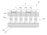
図1は、裏面照射型撮像デバイスが形成された被検査体としてのウェハの構成を概略的に示す平面図であり、図2は、裏面照射型撮像デバイスの構成を概略的に示す断面図である。
図1に示すように、裏面照射型撮像デバイスDは、略円板状のウェハWに複数形成されている。
FIG. 1 is a plan view schematically showing the configuration of a wafer as an object to be inspected on which a backside illumination imaging device is formed, and FIG. 2 is a cross-sectional view schematically showing the configuration of the backside illumination imaging device. be.
As shown in FIG. 1, a plurality of back-illuminated imaging devices D are formed on a substantially disk-shaped wafer W. As shown in FIG.
裏面照射型撮像デバイスDは、固体撮像素子であり、図2に示すように、フォトダイオードである光電変換部PDと、複数の配線PLaを含む配線層PLとを有する。また、裏面照射型撮像デバイスDは、配線層PL側をウェハWの表面側としたときに、ウェハWの裏面側から入射した光をオンチップレンズL及びカラーフィルタFを介して光電変換部PDで受光する。カラーフィルタFは赤色カラーフィルタFR、青色カラーフィルタFB及び緑色カラーフィルタFGからなる。 The back-illuminated imaging device D is a solid-state imaging device, and as shown in FIG. 2, has a photoelectric conversion unit PD that is a photodiode and a wiring layer PL that includes a plurality of wirings PLa. Further, in the back-illuminated imaging device D, when the wiring layer PL side is the front side of the wafer W, the light incident from the back side of the wafer W is transferred through the on-chip lens L and the color filter F to the photoelectric conversion unit PD. to receive light. The color filter F consists of a red color filter FR, a blue color filter FB and a green color filter FG.
また、裏面照射型撮像デバイスDの表面DaすなわちウェハWの表面には、電極Eが形成されており、該電極Eは配線層PLの配線PLaに電気的に接続されている。配線PLaは、裏面照射型撮像デバイスDの内部の回路素子に電気信号を入力したり、同回路素子からの電気信号を裏面照射型撮像デバイスDの外部に出力したりするためのものである。
なお、図1に示すように、ウェハWの外周部分には、裏面照射型撮像デバイスDが形成されていない非デバイス形成領域Rが存在する。
Further, an electrode E is formed on the surface Da of the back-illuminated imaging device D, that is, the surface of the wafer W, and the electrode E is electrically connected to the wiring PLa of the wiring layer PL. The wiring PLa is for inputting an electrical signal to a circuit element inside the back-illuminated imaging device D and for outputting an electrical signal from the circuit element to the outside of the back-illuminated imaging device D. FIG.
In addition, as shown in FIG. 1, the peripheral portion of the wafer W has a non-device forming region R in which the back-illuminated imaging device D is not formed.
(第1の実施形態)
続いて、第1の実施形態にかかる検査装置について説明する。
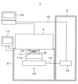
図3及び図4はそれぞれ、第1の実施形態にかかる検査装置としてのプローバ1の構成の概略を示す斜視図及び正面図である。図4では、図3のプローバ1の後述の収容室とローダが内蔵する構成要素を示すため、その一部が断面で示されている。
(First embodiment)
Next, an inspection apparatus according to the first embodiment will be described.
3 and 4 are a perspective view and a front view, respectively, showing an outline of the configuration of the
プローバ1は、ウェハWに形成された複数の裏面照射型撮像デバイスD(以下、撮像デバイスDと省略することがある。)それぞれの電気的特性の検査を行うものである。プローバ1は、図3及び図4に示すように、収容室2と、収容室2に隣接して配置されるローダ3と、収容室を覆うように配置されるテスタ4とを備える。
The
収容室2は、内部が空洞の筐体であり、ウェハWが載置される載置台としてのステージ10を有する。ステージ10は、該ステージ10に対するウェハWの位置がずれないように、ウェハWの外周部分の非デバイス形成領域R(図1参照)を挟持することにより、当該ウェハWを保持する。なお、ステージ10は、水平方向及び鉛直方向に移動自在に構成されており、後述のプローブカード11とウェハWの相対位置を調整してウェハWの表面の電極Eをプローブカード11のプローブ11aと接触させることができる。
The
また、収容室2における該ステージ10の上方には、該ステージ10に対向するようにプローブカード11が配置される。プローブカード11は、ウェハWの表面の電極Eに対応するように形成された多数の針状のプローブ11aを有する。
プローブカード11は、インターフェース12を介してテスタ4へ接続されている。各プローブ11aがウェハWの各撮像デバイスDの電極Eに接触する際、各プローブ11aは、テスタ4からインターフェース12を介して撮像デバイスDへ電力を供給し、または、撮像デバイスDからの信号をインターフェース12を介してテスタ4へ伝達する。
A
A
ローダ3は、搬送容器であるFOUP(図示せず)に収容されているウェハWを取り出して収容室2のステージ10へ搬送する。また、ローダ3は、撮像デバイスDの電気的特性の検査が終了したウェハWをステージ10から受け取り、FOUPへ収容する。
The
ローダ3は、電源等を制御するコントローラとしてのベースユニット13を有する。ベースユニット13は配線14を介してステージ10へ接続され、配線15を介してテスタコンピュータ16に接続されている。ベースユニット13は、テスタコンピュータ16からの入力信号に基づいて、ステージ10の後述の光照射部40による照射動作を制御する。また、ベースユニット13は、ステージ10の不図示の温度測定機構に基づいて、ステージ10の後述の温度調整機構50を制御する。なお、ベースユニット13は収容室2に設けられてもよい。
The
テスタ4は、撮像デバイスDが搭載されるマザーボードの回路構成の一部を再現するテストボード(図示せず)を有する。テストボードは、テスタコンピュータ16に接続される。テスタコンピュータ16は、撮像デバイスDからの信号に基づいて該撮像デバイスDの良否を判断する。テスタ4では、上記テストボードを取り替えることにより、複数種のマザーボードの回路構成を再現することができる。
The
さらに、プローバ1は、ユーザインターフェース部17を備える。ユーザインターフェース部17は、ユーザ向けに情報を表示したりユーザが指示を入力したりするためのものであり、例えば、タッチパネルやキーボード等を有する表示パネルからなる。
Further, the
上述の各部を有するプローバ1では、撮像デバイスDの電気的特性の検査の際、テスタコンピュータ16が、撮像デバイスDと各プローブ11aを介して接続されたテストボードへデータを送信する。そして、テスタコンピュータ16が、送信されたデータが当該テストボードによって正しく処理されたか否かを当該テストボードからの電気信号に基づいて判定する。
In the
次に、ステージ10の構成について説明する。図5はステージ10の構成を概略的に示す断面図である。
ステージ10は、撮像デバイスDの裏面と当該ステージ10とが対向する形態でウェハWが載置されるものであり、図5に示すように、透過部30と、光照射部40と、を有する。
Next, the configuration of the
The
透過部30は、光透過材料からなり、ウェハWの裏面が当接する形態で当該ウェハWが載置されるものであり、平板状の平板部材31を有する。なお、「光透過材料」とは、検査範囲の波長の光を透過する材料である。透過部30には、載置されたウェハWを保持するために、当該ウェハWの外周部分の非デバイス形成領域Rを挟持する挟持機構(図示せず)が設けられている。
The
光照射部40は、ウェハWに向けて光を照射するものであり、透過部30より鉛直方向下側の領域S1に配置されている。
光照射部40は、導光板41と光源部42とを有する。
The
The
導光板41は、透過部30を間に挟みウェハWと対向する対向面41aを有する平板状の部材である。導光板41は、例えば平面視において、ウェハWの直径より一辺の長さが大きい正方形状に形成される。本実施形態では、導光板41の強度を補うため、当該導光板41の下面に対してサポート部材43が設けられている。この導光板41は、後述するように面状の光をウェハWに向けて出射するものであるところ、平面視において、面状の光を出射する領域内に、ウェハWの撮像デバイス形成領域が含まれるように配置される。
The
光源部42は、導光板41の側方外側の領域S2に設けられており、導光板41の一側端面に向けて線状の光を出射する。光源部42は、線状の光を出射するため、例えば、導光板41の側端面に沿って設けられた複数のLED(Light Emitting Diode)から構成される。LEDは、例えば導光板41内で拡散され透過部30を透過した光が検査範囲の波長の光を含むような光を出射する。検査範囲の波長の光とは、例えば、可視光領域の波長の光であり、撮像デバイスDの種類によっては、赤外線等の可視光領域外の光を含む場合もある。
また、本実施形態では、光源部42のLEDの熱をステージ10の外部に放出するため、LEDを支持する基板(図示せず)の背面には放熱板44が設けられている。放熱板44は、例えば、金属材料から形成される。放熱板44には、光源部42のLEDを冷却するための水等の冷媒が通流する経路が形成されていてもよい。
The
Further, in this embodiment, in order to release the heat of the LEDs of the
プローバ1では、導光板41が、光源部42から出射され当該導光板41の側端面から入射された線状の光を、当該導光板41の内部で拡散させ、ウェハWと対向する対向面41aから面状の光で出射する。
In the
ここで、透過部30についてさらに説明する。
プローバ1において検査時にウェハWが載置される面には高い平坦性が用いられる。しかし、既製の導光板41の上面は平坦度が高くない。そこで、本実施形態では、光照射部40の導光板41の上部に、導光板41とは別に作製され高い平坦性を有する上面を備える透過部30が設けられている。
Here, the
The surface of the
透過部30は、導光板41からウェハWの方向に向けて出射された面状の光を、単純に透過するものであってもよいし、拡散させながら透過するものであってもよい。拡散させながら透過することにより、透過部30からウェハWに対して、光強度分布がさらに面内で均一な光を照射することができる。
The
透過部30は、光を拡散させながら透過するためには、例えば、平板部材31が透明ガラスからなり、そのウェハW側の面が砂ずり面とされる。これにより、透過部30に入射された導光板41からの光は、上記砂ずり面で拡散された状態で透過部30から出射される。
In order for the transmitting
また、透過部30は、光を拡散させながら透過するために、平板部材31を内部に気泡を含む気泡石英から形成してもよい。この透過部30を用いる場合、当該透過部30に入射された導光板41からの光は、当該透過部30内の気泡で拡散されつつ当該透過部30を通過し出射される。
Further, in order to transmit the light while diffusing the light, the
さらに、透過部30は、光を拡散させながら透過するために、平板部材31を焼結アルミナ等の透明セラミックから形成してもよい。透明セラミックは、その内部に粒界や欠陥を有する。そのため、本例の透過部30を用いる場合、当該透過部30に入射された導光板41からの光は、当該透過部30内の上述の粒界や欠陥で拡散されつつ当該透過部30を通過し出射される。
さらに、透過部30は、光を拡散させながら透過するために、平板部材31をホログラフィックディフューザーにより構成してもよい。ホログラフィックディフューザーは、石英ガラス基板等のガラス基板上にホログラムパターン
(約5μmの非周期な凹凸パターンの集まり)が形成されたものである。この透過部30を用いる場合、当該透過部30に入射された導光板41からの光は、平板部材31のホログラムパターンで拡散されつつ当該透過部30を通過し出射される。
Furthermore, in order to transmit light while diffusing the light, the
Furthermore, the
上述の透過部30と光照射部40を有するステージ10は、光照射部40より下側の領域S3に、具体的には、導光板41に対するサポート部材43より下側の領域S3に、ウェハWの温度調整機構50を有する。温度調整機構としては、既存の、温度調整機能を有するウェハWの載置台(以下、「温調ステージ」という。)を用いることができる。既存の温調ステージは、ウェハWの吸着機構を有するため、この吸着機構により、光照射部40が温度調整機構50に吸着保持される。なお、透過部30は例えば透明接着材料による接着保持により光照射部40に保持される。
The
次に、プローバ1を用いたウェハWに対する検査処理の一例について説明する。以下の説明では、1回の検査で1つの撮像デバイスDが検査されるものとする。ただし、プローバ1を用いた1回の検査で、複数の撮像デバイスDを一括して検査してもよい。
Next, an example of inspection processing for the wafer W using the
まず、ローダ3のFOUPからウェハWが取り出されて収容室2内に搬送される。そして、ウェハWは、当該ウェハWに形成された撮像デバイスDの裏面とステージ10とが対向すると共に当該ウェハWの裏面がステージ10と当接するように、ステージ10に載置される。
First, the wafer W is taken out from the FOUP of the
次いで、ステージ10が移動され、ステージ10の上方に設けられているプローブ11aと検査対象の撮像デバイスDの電極Eとが接触する。
Next, the
そして、光照射部40の光源部42のLEDが点灯され、光照射部40から、導光板41の側端面に光が入射する。導光板41に入射された光は、導光板41の内部で拡散され、ウェハWと対向する対向面41aから面上の光で出射する。出射された光は、透過部30を透過し、ウェハWに照射される。
このウェハWへの光の照射と共に、プローブ11aへの検査用の信号の入力が行われる。これにより、撮像デバイスDの検査を行う。なお、上記検査中、不図示の温度測定機構により、ウェハWの温度が測定され、その結果に基づいて、温度調整機構50が制御され、ウェハWの温度が所望の値に調整されることにより、撮像デバイスDの温度が所望の値に調整される。
以後、全ての撮像デバイスDの検査が完了するまで上述と同様な処理が繰り返される。
Then, the LED of the
When the wafer W is irradiated with light, an inspection signal is input to the
After that, the same processing as described above is repeated until the inspection of all imaging devices D is completed.
以上のように、本実施形態では、ステージ10が、光透過材料からなりウェハWが載置される透過部30と、透過部30より下側の領域S1に配置された光照射部40とを有する。そして、光照射部40が、透過部30を間に挟みウェハWと対向する対向面41aを有する導光板41と、導光板41の側方外側領域に設けられた光源部42とを有する。本実施形態では、導光板41が、光源部42から出射され当該導光板41の側端面から入射された光を、当該導光板41の内部で拡散させ、上記対向面41aから面状の光で出射する。そのため、裏面照射型撮像デバイスDを検査することができる。また、検査のための開口をプローブカード11に設ける必要がないため、プローブ11aの数が制限されないので、短時間で検査を行うことができる。さらに、本実施形態では、光源部42が導光板41の側方外側領域に設けられており、光源部42を配設するためにステージ10の内部に空洞を形成する必要がない。したがって、ステージ10の強度が損なわれることがない。特に、複数の撮像デバイスDを一括で検査する場合、ステージ10に大きな荷重が加わるため、ステージ10の強度は重要である。
As described above, in the present embodiment, the
また、本実施形態では、ステージ10が、導光板41より下側の領域に、温度調整機構50を有する。ウェハWの温度調整機構を、導光板41より上側の領域に設ける場合、具体的には、導光板41とウェハWの間に設ける場合、当該温度調整機構を光透過性材料で構成する必要がある。それに対し、ステージ10が、導光板41より下側の領域に、温度調整機構50を有するため、温度調整機構50に既存の温調ステージを用いることができる。
Further, in this embodiment, the
また、本実施形態では、複数のLEDからなる光源部42と導光板41により光照射部40を構成しているため、ステージ10の大型化を防ぎ、さらには収容室2やプローバ1の大型化を防ぐことができる。
In addition, in this embodiment, the
さらにまた、本実施形態では、ウェハWを保持するための機構として、ウェハWの外周部分の非デバイス形成領域Rを挟持する挟持機構を用いている。したがって、透過部30に吸着保持用の孔を形成する必要がないため、当該吸着保持用の孔が、ウェハWに照射する光の強度分布の面内均一性に影響を及ぼすのを防ぐことができる。
Furthermore, in this embodiment, as a mechanism for holding the wafer W, a clamping mechanism for clamping the non-device forming region R of the outer peripheral portion of the wafer W is used. Therefore, since it is not necessary to form a suction-holding hole in the transmitting
(第2の実施形態)
図6は、第2の実施形態にかかる検査装置としてのプローバが有するステージ10の構成を概略的に示す断面図である。
本実施形態のステージ10は、図6に示すように、透過部30が、光を透過する平板状の平板部材31の他に、低屈折率部32を有する。
(Second embodiment)
FIG. 6 is a cross-sectional view schematically showing the configuration of a
In the
低屈折率部32は、その屈折率が平板部材31より低いものであり、また、平板部材31に重なるように当該平板部材31よりもウェハW側に設けられ、ステージ10に載置されたウェハWはその裏面が当該低屈折率部32に当接する。例えば、平板部材31が石英ガラスからなる場合、低屈折率部32には平板部材31とは異なる種類の石英ガラス(例えば、不純物の種類や不純物の割合が異なる平板部材31とは異なる石英ガラス)が用いられる。これにより、低屈折率部32を平板部材31より低い屈折率とすることができる。
また、低屈折率部32の材料にフッ素樹脂を用い、当該フッ素樹脂に添加する材料を調整することにより、低屈折率部32を平板部材31より低屈折率とすることができる。
なお、電界を加えることにより屈折率が変化する電気光学効果を有する電気光学結晶から低屈折率部32を形成してもよい。
The low
Further, by using fluororesin as the material of the low
Alternatively, the low
低屈折率部32の形成は、当該低屈折率部32が石英ガラスや電気光学結晶の場合は例えばCVD法により行われ、また、当該低屈折率部32がフッ素樹脂の場合は、例えばスピンコーティング法により行われる。
The formation of the low
本実施形態では、平板部材31を透過した光のうち、低屈折率部32に対する入射角が小さいものは、低屈折率部32に入射され当該低屈折率部32を透過しウェハWに向けて出射される。しかし、低屈折率部32に対する入射角が大きい光は、低屈折率部32の平板部材31側の面で反射されるためウェハWには入射されない。このように、本実施形態では、平板部材31から低屈折率部32への光の入射角度が制限されるため、低屈折率部32を透過してウェハWに照射される光の入射角度も制限される。つまり、本実施形態では、ウェハWに照射する光の入射角度を制限することができる。したがって、プローバ1は、撮像デバイスDへ入射角度を制限する必要がある検査にも用いることができる。
In the present embodiment, out of the light transmitted through the
今回開示された実施形態はすべての点で例示であって制限的なものではないと考えられるべきである。上記の実施形態は、添付の請求の範囲及びその主旨を逸脱することなく、様々な形態で省略、置換、変更されてもよい。 It should be considered that the embodiments disclosed this time are illustrative in all respects and not restrictive. The embodiments described above may be omitted, substituted, or modified in various ways without departing from the scope and spirit of the appended claims.
なお、以下のような構成も本開示の技術的範囲に属する。 Note that the following configuration also belongs to the technical scope of the present disclosure.
(1)被検査デバイスを検査する検査装置であって、
被検査体に形成された被検査デバイスは、配線層が設けられた側とは反対側の面である裏面から光が入射される裏面照射型の撮像デバイスであり、
当該検査装置は、
前記撮像デバイスの裏面と対向する形態で前記被検査体が載置される載置台を有し、
前記載置台は、
光透過材料からなり、前記被検査体が載置される透過部と、
前記透過部より下側の領域に配置された、光照射部と、を有し、
前記光照射部は、
前記透過部を間に挟み前記被検査体と対向する対向面を有する、平板状の導光板と、
前記導光板の側方外側の領域に設けられた光源部と、
を有し、
前記導光板は、前記光源部から出射され当該導光板の側端面から入射された光を、当該導光板内部で拡散させ、前記被検査体と対向する前記対向面から面状の光で出射する、検査装置。
前記(1)によれば、裏面照射型撮像デバイスを検査することができる。また、検査のための開口をプローブカードに設ける必要がないため、プローブの数が制限されないので、短時間で検査を行うことができる。さらに、本実施形態では、光源部が導光板の側方外側領域に設けられており、光源部を配設するために載置台の内部に空洞を形成する必要がない。したがって、載置台の強度が損なわれることがない。
(1) An inspection apparatus for inspecting a device under inspection,
The device to be inspected formed on the object to be inspected is a back-illuminated imaging device in which light is incident from the back surface, which is the surface opposite to the side on which the wiring layer is provided,
The inspection device is
a mounting table on which the object to be inspected is mounted so as to face the back surface of the imaging device;
The mounting table is
a transmission part made of a light transmission material and on which the object to be inspected is mounted;
a light irradiation section disposed in a region below the transmission section;
The light irradiation unit is
a flat light guide plate having a facing surface facing the inspected object with the transmitting portion sandwiched therebetween;
a light source unit provided in a laterally outer region of the light guide plate;
has
The light guide plate diffuses the light emitted from the light source unit and incident from the side end surface of the light guide plate inside the light guide plate, and emits planar light from the facing surface facing the object to be inspected. , inspection equipment.
According to (1) above, it is possible to inspect a back-illuminated imaging device. In addition, since there is no need to provide an opening for inspection in the probe card, the number of probes is not limited, so inspection can be performed in a short time. Furthermore, in this embodiment, the light source section is provided in the lateral outer region of the light guide plate, so that it is not necessary to form a cavity inside the mounting table in order to dispose the light source section. Therefore, the strength of the mounting table is not impaired.
(2)前記透過部は、前記導光板からの光を拡散させながら透過する、前記(1)に記載の検査装置。
前記(2)によれば、透過部から被検査体に対して、光強度分布がより面内で均一な光を照射することができる。
(2) The inspection device according to (1), wherein the transmission section transmits the light from the light guide plate while diffusing it.
According to the above (2), it is possible to irradiate the object to be inspected with light having a more uniform light intensity distribution in the plane from the transmitting portion.
(3)前記載置台は、前記導光板より下側の領域に、前記被検査体の温度を調整する温度調整機構を有する、前記(1)または(2)に記載の検査装置。
前記(3)によれば、温度調整機構を光透過性材料で構成する必要がなく、既存の温調ステージ等、安価な構成とすることができる。
(3) The inspection apparatus according to (1) or (2), wherein the mounting table has a temperature adjustment mechanism for adjusting the temperature of the object to be inspected in a region below the light guide plate.
According to (3) above, there is no need to configure the temperature control mechanism with a light-transmitting material, and an existing temperature control stage or the like can be inexpensively configured.
(4)前記透過部は、透明材料からなる平板部材と、前記平板部材の上に設けられ屈折率が当該平板部材よりも低い低屈折率部と、を有する、前記(1)~(3)のいずれか1に記載の検査装置。 (4) The above (1) to (3), wherein the transmissive portion has a flat plate member made of a transparent material, and a low refractive index portion provided on the flat plate member and having a lower refractive index than the flat plate member. The inspection device according to any one of 1.
(5)被検査デバイスを検査する検査方法であって、
被検査体に形成された被検査デバイスは、配線層が設けられた側とは反対側の面である裏面から光が入射される裏面照射型の撮像デバイスであり、
当該検査方法は、
前記撮像デバイスの裏面と載置台の光透過材料からなる透過部とが対向するように、当該透過部上に前記被検査体を載置する工程と、
前記透過部より下側の領域であって前記透過部の側方外側の領域に設けられた光源から、前記透過部より下側の領域に、当該透過部を間に挟み前記被検査体と対向するように配置された、平板状の導光板の側端面に、光を入射する工程と、
前記光源から出射され前記導光板の側端面から入射された光を、当該導光板内部で拡散させ、当該導光板の前記被検査体と対向する面から面状の光で出射する工程と、を有する、検査方法。
(5) An inspection method for inspecting a device under inspection, comprising:
The device to be inspected formed on the object to be inspected is a back-illuminated imaging device in which light is incident from the back surface, which is the surface opposite to the side on which the wiring layer is provided,
The inspection method is
placing the object to be inspected on the transmissive portion of the mounting table so that the rear surface of the imaging device and the transmissive portion made of a light transmissive material face each other;
From the light source provided in the area below the transmission part and laterally outside the transmission part, the area below the transmission part faces the inspection object with the transmission part interposed therebetween. a step of injecting light into a side end face of a flat light guide plate arranged so as to
a step of diffusing the light emitted from the light source and incident from the side end surface of the light guide plate inside the light guide plate and emitting planar light from the surface of the light guide plate facing the object to be inspected; have an inspection method.
1 プローバ
10 ステージ
30 透過部
40 光照射部
41 導光板
41a 対向面
42 光源部
D 裏面照射型撮像デバイス
S1 領域
S2 領域
W ウェハ
1
Claims (6)
被検査体に形成された被検査デバイスは、配線層が設けられた側とは反対側の面である裏面から光が入射される裏面照射型の撮像デバイスであり、
当該検査装置は、
前記撮像デバイスの裏面と対向する形態で前記被検査体が載置される載置台を有し、
前記載置台は、
光透過材料からなり、前記被検査体が載置される透過部と、
前記透過部より下側の領域に配置された、光照射部と、を有し、
前記光照射部は、
前記透過部を間に挟み前記被検査体と対向する対向面を有する、平板状の導光板と、
前記導光板の側方外側の領域に設けられた光源部と、
を有し、
前記導光板は、
前記光源部から出射され当該導光板の側端面から入射された光を、当該導光板内部で拡散させ、前記被検査体と対向する前記対向面から面状の光で出射すると共に、
平面視で前記面状の光を放射する領域内に、前記被検査体における前記撮像デバイスが形成される領域が含まれるように配置され、
前記載置台の内部に空洞が形成されていない、検査装置。 An inspection apparatus for inspecting a device under inspection,
The device to be inspected formed on the object to be inspected is a back-illuminated imaging device in which light is incident from the back surface, which is the surface opposite to the side on which the wiring layer is provided,
The inspection device is
a mounting table on which the object to be inspected is mounted so as to face the back surface of the imaging device;
The mounting table is
a transmission part made of a light transmission material and on which the object to be inspected is placed;
a light irradiation section disposed in a region below the transmission section;
The light irradiation unit is
a flat light guide plate having a facing surface facing the inspected object with the transmitting portion sandwiched therebetween;
a light source unit provided in a laterally outer region of the light guide plate;
has
The light guide plate is
The light emitted from the light source unit and incident from the side end surface of the light guide plate is diffused inside the light guide plate and emitted as planar light from the facing surface facing the object to be inspected,
arranged so that the area where the imaging device is formed in the object to be inspected is included in the area that radiates the planar light in a plan view,
The inspection device, wherein no cavity is formed inside the mounting table .
被検査体に形成された被検査デバイスは、配線層が設けられた側とは反対側の面である裏面から光が入射される裏面照射型の撮像デバイスであり、
当該検査装置は、
前記撮像デバイスの裏面と対向する形態で前記被検査体が載置される載置台を有し、
前記載置台は、
光透過材料からなり、前記被検査体が載置される透過部と、
前記透過部より下側の領域に配置された、光照射部と、を有し、
前記光照射部は、
前記透過部を間に挟み前記被検査体と対向する対向面を有する、平板状の導光板と、
前記導光板の側方外側の領域に設けられた光源部と、
を有し、
前記導光板は、前記光源部から出射され当該導光板の側端面から入射された光を、当該導光板内部で拡散させ、前記被検査体と対向する前記対向面から面状の光で出射し、
前記透過部は、透明材料からなる平板部材と、前記平板部材の上に設けられ屈折率が当該平板部材よりも低い低屈折率部と、を有する、検査装置。 An inspection apparatus for inspecting a device under inspection,
The device to be inspected formed on the object to be inspected is a back-illuminated imaging device in which light is incident from the back surface, which is the surface opposite to the side on which the wiring layer is provided,
The inspection device is
a mounting table on which the object to be inspected is mounted so as to face the back surface of the imaging device;
The mounting table is
a transmission part made of a light transmission material and on which the object to be inspected is mounted;
a light irradiation section disposed in a region below the transmission section;
The light irradiation unit is
a flat light guide plate having a facing surface facing the inspected object with the transmitting portion sandwiched therebetween;
a light source unit provided in a laterally outer region of the light guide plate;
has
The light guide plate diffuses the light emitted from the light source unit and incident from the side end surface of the light guide plate inside the light guide plate, and emits planar light from the facing surface facing the object to be inspected. ,
The inspection device, wherein the transmission section includes a flat plate member made of a transparent material, and a low refractive index portion provided on the flat plate member and having a lower refractive index than the flat plate member.
被検査体に形成された被検査デバイスは、配線層が設けられた側とは反対側の面である裏面から光が入射される裏面照射型の撮像デバイスであり、
当該検査方法は、
前記撮像デバイスの裏面と内部に空洞が形成されていない載置台の光透過材料からなる透過部とが対向するように、当該透過部上に前記被検査体を載置する工程と、
前記透過部より下側の領域であって前記透過部の側方外側の領域に設けられた光源から、前記透過部より下側の領域に、当該透過部を間に挟み前記被検査体と対向するように配置された、平板状の導光板の側端面に、光を入射する工程と、
前記光源から出射され前記導光板の側端面から入射された光を、当該導光板内部で拡散させ、当該導光板の前記被検査体と対向する面から面状の光で出射する工程と、を有し、
前記載置する工程は、平面視において、前記導光板における前記面状の光を放射する領域内に、前記撮像デバイスが形成される領域が含まれるように、前記被検査体を載置する、検査方法。 An inspection method for inspecting a device under inspection, comprising:
The device to be inspected formed on the object to be inspected is a back-illuminated imaging device in which light is incident from the back surface, which is the surface opposite to the side on which the wiring layer is provided,
The inspection method is
placing the object to be inspected on the transmissive portion such that the back surface of the imaging device and the transmissive portion made of a light transmissive material of the mounting table without a cavity formed therein face each other;
From the light source provided in the area below the transmission part and laterally outside the transmission part, the area below the transmission part faces the inspection object with the transmission part interposed therebetween. a step of injecting light into a side end face of a flat light guide plate arranged so as to
a step of diffusing the light emitted from the light source and incident from the side end surface of the light guide plate inside the light guide plate and emitting planar light from the surface of the light guide plate facing the object to be inspected; have
In the step of placing, in a plan view, the object to be inspected is placed so that an area in which the imaging device is formed is included in an area of the light guide plate that emits planar light. Inspection method.
Priority Applications (4)
| Application Number | Priority Date | Filing Date | Title |
|---|---|---|---|
| JP2018201073A JP7236840B2 (en) | 2018-10-25 | 2018-10-25 | Inspection device and inspection method |
| PCT/JP2019/040936 WO2020085203A1 (en) | 2018-10-25 | 2019-10-17 | Inspection device and inspection method |
| KR1020217014859A KR102559306B1 (en) | 2018-10-25 | 2019-10-17 | Inspection device and inspection method |
| US17/286,959 US11940485B2 (en) | 2018-10-25 | 2019-10-17 | Inspection apparatus and inspection method |
Applications Claiming Priority (1)
| Application Number | Priority Date | Filing Date | Title |
|---|---|---|---|
| JP2018201073A JP7236840B2 (en) | 2018-10-25 | 2018-10-25 | Inspection device and inspection method |
Publications (2)
| Publication Number | Publication Date |
|---|---|
| JP2020068333A JP2020068333A (en) | 2020-04-30 |
| JP7236840B2 true JP7236840B2 (en) | 2023-03-10 |
Family
ID=70332065
Family Applications (1)
| Application Number | Title | Priority Date | Filing Date |
|---|---|---|---|
| JP2018201073A Active JP7236840B2 (en) | 2018-10-25 | 2018-10-25 | Inspection device and inspection method |
Country Status (4)
| Country | Link |
|---|---|
| US (1) | US11940485B2 (en) |
| JP (1) | JP7236840B2 (en) |
| KR (1) | KR102559306B1 (en) |
| WO (1) | WO2020085203A1 (en) |
Families Citing this family (4)
| Publication number | Priority date | Publication date | Assignee | Title |
|---|---|---|---|---|
| JP7396683B2 (en) | 2021-02-23 | 2023-12-12 | リードテクノ株式会社 | Piezoelectric constant measuring device and piezoelectric constant measuring method |
| JP2023148394A (en) * | 2022-03-30 | 2023-10-13 | 東京エレクトロン株式会社 | Inspection device |
| WO2023234049A1 (en) * | 2022-06-01 | 2023-12-07 | 東京エレクトロン株式会社 | Inspection apparatus and mounting base |
| JP2023177133A (en) * | 2022-06-01 | 2023-12-13 | 東京エレクトロン株式会社 | Inspection device and inspection method |
Citations (2)
| Publication number | Priority date | Publication date | Assignee | Title |
|---|---|---|---|---|
| JP2004287368A (en) | 2003-01-27 | 2004-10-14 | Tokyo Electron Ltd | Inspecting device |
| JP2009170730A (en) | 2008-01-17 | 2009-07-30 | Fujifilm Corp | Inspecting apparatus for back irradiating type solid-state imaging device |
Family Cites Families (6)
| Publication number | Priority date | Publication date | Assignee | Title |
|---|---|---|---|---|
| US5613751A (en) * | 1995-06-27 | 1997-03-25 | Lumitex, Inc. | Light emitting panel assemblies |
| JP2005044853A (en) | 2003-07-23 | 2005-02-17 | Inter Action Corp | Inspection device of solid state imaging device |
| JP2005235839A (en) * | 2004-02-17 | 2005-09-02 | Canon Inc | Method and apparatus of inspecting chip wafer of semiconductor device |
| TW201009364A (en) * | 2008-08-28 | 2010-03-01 | King Yuan Electronics Co Ltd | Test socket and test module |
| US9411013B2 (en) * | 2014-02-14 | 2016-08-09 | Google, Inc. | Instrument for automated testing of displays |
| JP6994313B2 (en) | 2016-11-29 | 2022-01-14 | 東京エレクトロン株式会社 | Mounting table and electronic device inspection equipment |
-
2018
- 2018-10-25 JP JP2018201073A patent/JP7236840B2/en active Active
-
2019
- 2019-10-17 WO PCT/JP2019/040936 patent/WO2020085203A1/en active Application Filing
- 2019-10-17 KR KR1020217014859A patent/KR102559306B1/en active IP Right Grant
- 2019-10-17 US US17/286,959 patent/US11940485B2/en active Active
Patent Citations (2)
| Publication number | Priority date | Publication date | Assignee | Title |
|---|---|---|---|---|
| JP2004287368A (en) | 2003-01-27 | 2004-10-14 | Tokyo Electron Ltd | Inspecting device |
| JP2009170730A (en) | 2008-01-17 | 2009-07-30 | Fujifilm Corp | Inspecting apparatus for back irradiating type solid-state imaging device |
Also Published As
| Publication number | Publication date |
|---|---|
| WO2020085203A1 (en) | 2020-04-30 |
| KR20210072820A (en) | 2021-06-17 |
| US20210389366A1 (en) | 2021-12-16 |
| JP2020068333A (en) | 2020-04-30 |
| KR102559306B1 (en) | 2023-07-26 |
| US11940485B2 (en) | 2024-03-26 |
Similar Documents
| Publication | Publication Date | Title |
|---|---|---|
| JP7236840B2 (en) | Inspection device and inspection method | |
| TWI767093B (en) | Inspection device | |
| TWI733356B (en) | Test device, test method and computer readable medium | |
| US7642792B2 (en) | Probe card for tests on photosensitive chips and corresponding illumination device | |
| TW201500750A (en) | Wafer testing machine | |
| JP7186060B2 (en) | Inspection device and inspection method | |
| TW202234079A (en) | Test apparatus, test method, and computer-readable storage medium | |
| WO2020095699A1 (en) | Inspection apparatus and inspection method | |
| CN104035016B (en) | Method for the probe card and manufacture probe card of test wafer | |
| WO2023234048A1 (en) | Testing apparatus and testing method | |
| WO2023234049A1 (en) | Inspection apparatus and mounting base | |
| TW202412132A (en) | Inspection equipment and inspection methods | |
| JP2006329816A (en) | Probe inspection device | |
| JP2023177195A (en) | Inspection apparatus and mounting table | |
| JP2023035742A (en) | Inspection device and inspection method | |
| TW202412131A (en) | Inspection device and mounting table | |
| WO2023189675A1 (en) | Inspection apparatus | |
| TW202217328A (en) | Inspection equipment and method for controlling inspection equipment | |
| KR100923253B1 (en) | Illumination unit and test apparatus having the same |
Legal Events
| Date | Code | Title | Description |
|---|---|---|---|
| A621 | Written request for application examination |
Free format text: JAPANESE INTERMEDIATE CODE: A621 Effective date: 20210614 |
|
| A131 | Notification of reasons for refusal |
Free format text: JAPANESE INTERMEDIATE CODE: A131 Effective date: 20220809 |
|
| A521 | Request for written amendment filed |
Free format text: JAPANESE INTERMEDIATE CODE: A523 Effective date: 20221004 |
|
| TRDD | Decision of grant or rejection written | ||
| A01 | Written decision to grant a patent or to grant a registration (utility model) |
Free format text: JAPANESE INTERMEDIATE CODE: A01 Effective date: 20230131 |
|
| A61 | First payment of annual fees (during grant procedure) |
Free format text: JAPANESE INTERMEDIATE CODE: A61 Effective date: 20230228 |
|
| R150 | Certificate of patent or registration of utility model |
Ref document number: 7236840 Country of ref document: JP Free format text: JAPANESE INTERMEDIATE CODE: R150 |