JP7233082B2 - Optical element, microlens array, and method for fabricating optical element - Google Patents
Optical element, microlens array, and method for fabricating optical element Download PDFInfo
- Publication number
- JP7233082B2 JP7233082B2 JP2018243598A JP2018243598A JP7233082B2 JP 7233082 B2 JP7233082 B2 JP 7233082B2 JP 2018243598 A JP2018243598 A JP 2018243598A JP 2018243598 A JP2018243598 A JP 2018243598A JP 7233082 B2 JP7233082 B2 JP 7233082B2
- Authority
- JP
- Japan
- Prior art keywords
- electrode layer
- optical element
- voltage
- electrode
- material layer
- Prior art date
- Legal status (The legal status is an assumption and is not a legal conclusion. Google has not performed a legal analysis and makes no representation as to the accuracy of the status listed.)
- Active
Links
Images


Classifications
-
- F—MECHANICAL ENGINEERING; LIGHTING; HEATING; WEAPONS; BLASTING
- F21—LIGHTING
- F21V—FUNCTIONAL FEATURES OR DETAILS OF LIGHTING DEVICES OR SYSTEMS THEREOF; STRUCTURAL COMBINATIONS OF LIGHTING DEVICES WITH OTHER ARTICLES, NOT OTHERWISE PROVIDED FOR
- F21V5/00—Refractors for light sources
- F21V5/002—Refractors for light sources using microoptical elements for redirecting or diffusing light
- F21V5/004—Refractors for light sources using microoptical elements for redirecting or diffusing light using microlenses
-
- G—PHYSICS
- G02—OPTICS
- G02F—OPTICAL DEVICES OR ARRANGEMENTS FOR THE CONTROL OF LIGHT BY MODIFICATION OF THE OPTICAL PROPERTIES OF THE MEDIA OF THE ELEMENTS INVOLVED THEREIN; NON-LINEAR OPTICS; FREQUENCY-CHANGING OF LIGHT; OPTICAL LOGIC ELEMENTS; OPTICAL ANALOGUE/DIGITAL CONVERTERS
- G02F1/00—Devices or arrangements for the control of the intensity, colour, phase, polarisation or direction of light arriving from an independent light source, e.g. switching, gating or modulating; Non-linear optics
- G02F1/01—Devices or arrangements for the control of the intensity, colour, phase, polarisation or direction of light arriving from an independent light source, e.g. switching, gating or modulating; Non-linear optics for the control of the intensity, phase, polarisation or colour
- G02F1/13—Devices or arrangements for the control of the intensity, colour, phase, polarisation or direction of light arriving from an independent light source, e.g. switching, gating or modulating; Non-linear optics for the control of the intensity, phase, polarisation or colour based on liquid crystals, e.g. single liquid crystal display cells
- G02F1/133—Constructional arrangements; Operation of liquid crystal cells; Circuit arrangements
- G02F1/1333—Constructional arrangements; Manufacturing methods
- G02F1/1334—Constructional arrangements; Manufacturing methods based on polymer dispersed liquid crystals, e.g. microencapsulated liquid crystals
-
- G—PHYSICS
- G02—OPTICS
- G02B—OPTICAL ELEMENTS, SYSTEMS OR APPARATUS
- G02B13/00—Optical objectives specially designed for the purposes specified below
- G02B13/001—Miniaturised objectives for electronic devices, e.g. portable telephones, webcams, PDAs, small digital cameras
- G02B13/0055—Miniaturised objectives for electronic devices, e.g. portable telephones, webcams, PDAs, small digital cameras employing a special optical element
- G02B13/0075—Miniaturised objectives for electronic devices, e.g. portable telephones, webcams, PDAs, small digital cameras employing a special optical element having an element with variable optical properties
-
- G—PHYSICS
- G02—OPTICS
- G02B—OPTICAL ELEMENTS, SYSTEMS OR APPARATUS
- G02B26/00—Optical devices or arrangements for the control of light using movable or deformable optical elements
- G02B26/004—Optical devices or arrangements for the control of light using movable or deformable optical elements based on a displacement or a deformation of a fluid
-
- G—PHYSICS
- G02—OPTICS
- G02B—OPTICAL ELEMENTS, SYSTEMS OR APPARATUS
- G02B26/00—Optical devices or arrangements for the control of light using movable or deformable optical elements
- G02B26/06—Optical devices or arrangements for the control of light using movable or deformable optical elements for controlling the phase of light
-
- G—PHYSICS
- G02—OPTICS
- G02B—OPTICAL ELEMENTS, SYSTEMS OR APPARATUS
- G02B26/00—Optical devices or arrangements for the control of light using movable or deformable optical elements
- G02B26/08—Optical devices or arrangements for the control of light using movable or deformable optical elements for controlling the direction of light
-
- G—PHYSICS
- G02—OPTICS
- G02B—OPTICAL ELEMENTS, SYSTEMS OR APPARATUS
- G02B3/00—Simple or compound lenses
- G02B3/0006—Arrays
-
- G—PHYSICS
- G02—OPTICS
- G02B—OPTICAL ELEMENTS, SYSTEMS OR APPARATUS
- G02B3/00—Simple or compound lenses
- G02B3/0006—Arrays
- G02B3/0037—Arrays characterized by the distribution or form of lenses
- G02B3/0056—Arrays characterized by the distribution or form of lenses arranged along two different directions in a plane, e.g. honeycomb arrangement of lenses
-
- G—PHYSICS
- G02—OPTICS
- G02B—OPTICAL ELEMENTS, SYSTEMS OR APPARATUS
- G02B3/00—Simple or compound lenses
- G02B3/0081—Simple or compound lenses having one or more elements with analytic function to create variable power
-
- G—PHYSICS
- G02—OPTICS
- G02B—OPTICAL ELEMENTS, SYSTEMS OR APPARATUS
- G02B3/00—Simple or compound lenses
- G02B3/12—Fluid-filled or evacuated lenses
- G02B3/14—Fluid-filled or evacuated lenses of variable focal length
-
- G—PHYSICS
- G02—OPTICS
- G02B—OPTICAL ELEMENTS, SYSTEMS OR APPARATUS
- G02B5/00—Optical elements other than lenses
- G02B5/02—Diffusing elements; Afocal elements
-
- G—PHYSICS
- G02—OPTICS
- G02B—OPTICAL ELEMENTS, SYSTEMS OR APPARATUS
- G02B5/00—Optical elements other than lenses
- G02B5/02—Diffusing elements; Afocal elements
- G02B5/0205—Diffusing elements; Afocal elements characterised by the diffusing properties
- G02B5/021—Diffusing elements; Afocal elements characterised by the diffusing properties the diffusion taking place at the element's surface, e.g. by means of surface roughening or microprismatic structures
-
- G—PHYSICS
- G02—OPTICS
- G02B—OPTICAL ELEMENTS, SYSTEMS OR APPARATUS
- G02B5/00—Optical elements other than lenses
- G02B5/02—Diffusing elements; Afocal elements
- G02B5/0273—Diffusing elements; Afocal elements characterized by the use
- G02B5/0278—Diffusing elements; Afocal elements characterized by the use used in transmission
-
- G—PHYSICS
- G03—PHOTOGRAPHY; CINEMATOGRAPHY; ANALOGOUS TECHNIQUES USING WAVES OTHER THAN OPTICAL WAVES; ELECTROGRAPHY; HOLOGRAPHY
- G03B—APPARATUS OR ARRANGEMENTS FOR TAKING PHOTOGRAPHS OR FOR PROJECTING OR VIEWING THEM; APPARATUS OR ARRANGEMENTS EMPLOYING ANALOGOUS TECHNIQUES USING WAVES OTHER THAN OPTICAL WAVES; ACCESSORIES THEREFOR
- G03B2205/00—Adjustment of optical system relative to image or object surface other than for focusing
- G03B2205/0053—Driving means for the movement of one or more optical element
- G03B2205/0084—Driving means for the movement of one or more optical element using other types of actuators
-
- H—ELECTRICITY
- H04—ELECTRIC COMMUNICATION TECHNIQUE
- H04N—PICTORIAL COMMUNICATION, e.g. TELEVISION
- H04N23/00—Cameras or camera modules comprising electronic image sensors; Control thereof
- H04N23/57—Mechanical or electrical details of cameras or camera modules specially adapted for being embedded in other devices
Description
本発明は、光学素子、マイクロレンズアレイ、及び光学素子の作製方法に関する。 The present invention relates to optical elements, microlens arrays, and methods of making optical elements.
従来から、電圧の印加によって変形する高分子材料を用いて、レンズを光軸方向に移動させる焦点調節機構(たとえば、特許文献1参照)、レンズ駆動機構(たとえば、特許文献2参照)等が知られている。高分子材料はレンズを保持するレンズホルダに用いられており、電圧印加による高分子材料の伸縮を利用して、レンズの位置を光軸に沿って動かしている。 Conventionally, a focus adjustment mechanism (see, for example, Patent Document 1) and a lens driving mechanism (see, for example, Patent Document 2) that move a lens in the optical axis direction using a polymeric material that deforms when voltage is applied are known. It is A polymer material is used for a lens holder that holds a lens, and the position of the lens is moved along the optical axis by utilizing the expansion and contraction of the polymer material due to voltage application.
また、電界の印加方向に伸縮する有機材料を一対の電極で挟み、有機材料層の電界印加方向と垂直な面内で単位電場当たりの電歪性歪量に分布を持たせることで、有機材料層と電極を変形させて凸レンズ、凹レンズ等を形成する方法が提案されている(たとえば、特許文献3参照)。 In addition, by sandwiching an organic material that expands and contracts in the direction of electric field application between a pair of electrodes and giving a distribution to the amount of electrostrictive strain per unit electric field in the plane perpendicular to the direction of electric field application of the organic material layer, the organic material A method has been proposed in which layers and electrodes are deformed to form a convex lens, a concave lens, or the like (see, for example, Patent Document 3).
人工筋肉アクチュエータに適用される高分子柔軟アクチュエータとして、ポリ塩化ビニル1~50重量部に対してイオン液体を1~30重量部含むゲル材料が知られている(たとえば特許文献4参照)。 Gel materials containing 1 to 30 parts by weight of ionic liquid with 1 to 50 parts by weight of polyvinyl chloride are known as soft polymer actuators applied to artificial muscle actuators (see, for example, Patent Document 4).
レンズを光軸に沿って移動させる構成は、レンズホルダに配置された高分子材料を伸縮させることで、単一のレンズの位置を変化させている。この構成は、まずホルダを変形させ、ホルダの変形によってレンズ位置を変えるので、レンズ駆動の応答性と精度を十分に高めることが難しい。 The configuration for moving the lens along the optical axis changes the position of a single lens by stretching the polymeric material placed in the lens holder. In this configuration, the holder is deformed first, and the lens position is changed by the deformation of the holder. Therefore, it is difficult to sufficiently improve the responsiveness and accuracy of driving the lens.
有機材料層の面内方向に電歪性歪量の分布を持たせる構成は、インクジェットやマイクロコンタクトプリンティングなどで、特性の異なる材料を微小量ずつ所望の位置に塗布するため、レンズ作製の工程が複雑であり時間がかかる。 The configuration in which the amount of electrostrictive strain is distributed in the in-plane direction of the organic material layer is achieved by applying minute amounts of materials with different properties to the desired positions by inkjet or microcontact printing, which increases the lens manufacturing process. Complex and time consuming.
また、上述した従来構成はいずれも単一のレンズの調整を目的としているが、イメージングや映像関連製品では、多数の微細なレンズを用いたマイクロレンズアレイに対する需要が高まっている。マイクロレンズアレイに焦点調整機能を付与することができれば、付加価値を高めることができる。 In addition, although the conventional configurations described above all aim to adjust a single lens, there is an increasing demand for microlens arrays using a large number of fine lenses in imaging and video-related products. If the microlens array can be provided with a focus adjustment function, the added value can be increased.
上記の課題に鑑みて、本発明は、簡単な構成で光学特性を調整することのできる光学素子とその作製方法を提供することを目的とする。 SUMMARY OF THE INVENTION In view of the above problems, an object of the present invention is to provide an optical element capable of adjusting optical characteristics with a simple configuration, and a method of manufacturing the same.
本発明では、電圧印加による高分子材料の伸縮または変形を利用して、光学素子の表面に光散乱体を形成する。 In the present invention, a light scatterer is formed on the surface of an optical element by utilizing expansion/contraction or deformation of a polymer material due to voltage application.
第1の態様では、第1の電極層と、第2の電極層と、前記第1の電極層と前記第2の電極層の間に配置される高分子材料層とを有する光学素子は、電圧印加の下で前記高分子材料層が変形して前記光学素子の表面に光散乱体が形成される。 In a first aspect, an optical element comprising a first electrode layer, a second electrode layer, and a polymer material layer disposed between the first electrode layer and the second electrode layer, Under voltage application, the polymeric material layer is deformed to form a light scatterer on the surface of the optical element.
第2の態様では、光学素子の作製方法は、
第1の電極層の上に高分子材料層を形成し、
前記高分子材料層の上に、第2の電極層を配置し、
前記第1の電極層と前記第2の電極層の間に電圧を印加して前記高分子材料層を変形させて、前記第2の電極層の表面に前記高分子材料層の一部を突出させて光散乱体を形成する、
工程を含む。
In a second aspect, a method for making an optical element comprises:
forming a polymeric material layer over the first electrode layer;
disposing a second electrode layer on the polymeric material layer;
A voltage is applied between the first electrode layer and the second electrode layer to deform the polymer material layer so that a part of the polymer material layer protrudes from the surface of the second electrode layer. to form a light scatterer,
Including process.
上記の構成と手法により、簡単な構成で光学特性を調整することのできる光学素子とその作製方法が実現される。 With the above configuration and method, an optical element capable of adjusting optical characteristics with a simple configuration and a manufacturing method thereof are realized.
図1は、実施形態の光学素子10の基本構成図である。光学素子10は、一対の電極12と電極13の間に、高分子材料層11が挟持された三層の積層構造を有する。電極12と電極13の間に電圧が印加された状態で、少なくとも一方の電極(たとえば電極13)の表面13sに、光散乱体15を有する。光散乱体15は、高分子材料層11と同じ材料で形成されている。
FIG. 1 is a basic configuration diagram of an
高分子材料層11と光散乱体15は、ゲル状のポリマー材料(以下、適宜「ポリマーゲル」と呼ぶ)で形成されている。光散乱体15は、電圧の印加によるポリマーゲルの伸縮または変形を利用して形成されている。図1(A)の例では、光散乱体15は、凸形状を有する。本明細書及び特許請求の範囲で「凸形状」というときは、とは、変形したポリマーゲルの少なくとも一部が電極の表面13s(ゼロ面)から上方に少なくとも一部が突出した状態を意味し、図1(A)のようにすべてが突出した状態に限られるものではない。
The
図1(B)及び図1(C)に示すように、凸形の光散乱体の中央付近が凹状にくぼんだ形状も、光散乱体15全体としてみたときに電極13の開口14から突出しており、光散乱効果を有する。図1(B)のように、光散乱体15Aの頂点がわずかにくぼんだ状態だけではなく、図1(C)のように、光散乱体15Bの中央部が電極13の表面13sよりも下方にある場合も、「凸形状」に含まれる。
As shown in FIGS. 1(B) and 1(C), the shape in which the vicinity of the center of the convex light scatterer is concave also protrudes from the
ポリマーゲルは、ポリ塩化ビニル(PVC:polyvinyl chloride)、ポリメタクリル酸メチル、ポリウレタン、ポリスチレン、ポリ酢酸ビニル、ポリビニルアルコール、ポリカーボネート、ポリエチレンテレフタレート、ポリアクリロニトリル、シリコーンゴム等であり、使用波長に対して透明な高分子(または樹脂)材料を適宜選択することができる。 Polymer gels are polyvinyl chloride (PVC), polymethyl methacrylate, polyurethane, polystyrene, polyvinyl acetate, polyvinyl alcohol, polycarbonate, polyethylene terephthalate, polyacrylonitrile, silicone rubber, etc., and are transparent to the wavelength used. A high polymer (or resin) material can be appropriately selected.
実施形態では、電場の作用による変形例が大きく、取扱いが容易なPVCを用いる。PVCに適切な可塑剤を添加してもよいし、PVCを溶媒に溶解させてもよい。可塑剤を用いる場合は、アジピン酸ジブチル(DBA:dibutyl adipate)、アジピン酸ジエチル(DEA:diethyl adipate)、セバシン酸ジエチル(DES:diethyl sebacate)、フタル酸ジオクチル(DOP:dioctyl phthalate)、フタル酸ジエチル(DEP:diethyl phthalate)等を用いることができる。溶媒として、テトラヒドロフラン(THF)等を用いることができる。 In the embodiment, PVC is used because it is highly deformable by the action of an electric field and is easy to handle. A suitable plasticizer may be added to PVC, or PVC may be dissolved in a solvent. When using a plasticizer, dibutyl adipate (DBA), diethyl adipate (DEA), diethyl sebacate (DES), dioctyl phthalate (DOP), diethyl phthalate (DEP: diethyl phthalate) or the like can be used. Tetrahydrofuran (THF) or the like can be used as a solvent.
可塑剤の混合比率は50wt%以上、好ましくは75wt%以上である。混合比率が50wt%未満だと、電圧を印加しても高分子材料層11を変形させることが困難になる。混合比率が50wt%以上75wt%未満のときは、電圧印加により高分子材料層11を変形させることができるが、印加する電圧レベルが高くなるおそれがある。混合比率を75wt%以上とすることで、適切な電圧レベルで高分子材料層11を変形させることができる。
The mixing ratio of the plasticizer is 50 wt% or more, preferably 75 wt% or more. If the mixing ratio is less than 50 wt %, it becomes difficult to deform the
電極12と電極13は、導電性を有する材料であれば、特に制限はない。電極12と電極13の少なくとも一方を金属で形成する場合は、白金、金、銀、ニッケル、クロム、銅、チタン、タンタル、インジウム、パラジウム、リチウム、ニオブ、これらの合金などを用いることができる。電極12と電極13の少なくとも一方をITO(Indium Tin Oxide:酸化インジウムスズ)等の透明な酸化物半導体材料で形成してもよいし、導電性ポリマー、導電性カーボン等を用いてもよい。
The
電極12と電極13の極性は、高分子材料層11の形状を変化させる方向に応じて設定することができる。図1(A)~図1(C)の例では、電極12は陰極層、電極13は陽極層である。電極12と電極13は、高分子材料層11と面接触している。
The polarities of the
電極13は開口14を有し、電圧が印加された状態で、光散乱体15、15A、及び15Bが、開口14から電極13の表面13sを超えて突出している。開口14の径は、光学素子10の用途に応じて適宜設定することができるが、1mm未満、好ましくは300μm以下である。開口14の径が1mm以上になると、電圧の印加によってポリマーゲルを開口14から突出させることが困難になる。開口の径が300μm以下とすることで、電圧印加に対するポリマーゲルの変形効率を高め、開口14の中心に対してほぼ均等な凸形状を形成することができる。
The
開口14の形状は、円、楕円、多角形等、目的に応じて決定することができる。
The shape of the
光学素子10の作製方法としては、所定の寸法に形成された電極12の上に、可塑剤が添加されたPVCの溶液をキャスト法等で塗布して、高分子材料層11を形成する。高分子材料層11の上で、あらかじめ開口14のパターンを形成した電極13を配置する。電極12と電極13の間に所定の電圧を印加して、電極13の表面に光散乱体15、15A、または15Bを形成する。
As a method for manufacturing the
高分子材料層11の厚さは、開口14のサイズ、形成したい光散乱体15の高さh、用いる電極12,13の厚さ等に応じて適宜決定されるが、一例として、1mm以下、好ましくは0.1mm~0.5mmである。高分子材料層11の厚さが0.1mm以下のときは多少ハンドリングしにくくなるが、あくまでも電極13の開口サイズとの兼ね合いがあるので、微細な多数のレンズを有するマイクロレンズアレイシートを作製する場合は、高分子材料層11の厚さが0.1mm以下になる場合もあり得る。
The thickness of the
図2は、図1(A)の形状を例にとって、実施形態の光学素子10の動作原理を説明する図である。図2(A)は電圧が印加されていない状態を示す。図2(B)は電圧が印加されたときの状態を示す。
FIG. 2 is a diagram for explaining the principle of operation of the
図2(A)の状態では、高分子材料層11は表面がフラットな状態で開口14の内部にある。このときの高分子材料層11の表面位置は、高さ方向(積層方向)で電極13の表面13sよりも低い。電極13の表面13sを高さ方向のゼロ面とする。
In the state of FIG. 2A, the
図2(B)のように、電極12と電極13の間に電圧が印加されると、陰極である電極12からポリマーゲルの高分子材料層11に電子が注入される。電子を含むポリマーゲルは陽極である電極13の開口14の端面に引き付けられる。ゲルの弾性により、微細な開口14で圧縮された分のポリマーゲルが開口14の中央から押し上げられ、電極13の表面13sから突出し、光散乱体15が形成される。
As shown in FIG. 2B, when a voltage is applied between the
ポリマーゲルの変形は、ゲルの弾性と電圧応答特性に基づくものであり、開口14から隆起して、開口14の中心に対して点対称な突起となる。高分子材料層11の組成が均一であれば、同じレベルの電圧を印加することで、ばらつきの少ない凸形状の光散乱体15を形成することができる。
The deformation of the polymer gel is based on the gel's elasticity and voltage response characteristics, and rises from the
トータルのポリマーゲルの体積は同じであるから、開口14からポリマーゲルが突出した分だけ、高分子材料層11の厚さが若干、低減する。高分子材料層11の厚さが低減すると、高分子材料層11と面接触している電極13の位置も下方に下がる。
Since the total volume of the polymer gel is the same, the thickness of the
高分子材料層11の変形は可逆的であり、電圧の印加を停止することで、図2(B)の初期状態に戻すことができる。また、後述するように、印加する電圧のレベルに応じて、光散乱体15の高さhを調整することができる。
The deformation of the
図3は、光学素子10の変形例である光学素子10Aの模式図である。光学素子10Aでは、図1の金属等の電極13に替えて、絶縁体16を導電膜17でコーティングした電極13Aを陽極として用いる。絶縁体16は、二酸化ケイ素、アルミナセラミクス等の無機絶縁体や、絶縁樹脂を用いることができる。導電膜17は、白金、金、銀、ニッケル、クロム、銅、チタン、タンタル、インジウム、パラジウム、リチウム、ニオブ、これらの合金などの薄膜、導電性のポリマー、導電性カーボン、酸化物半導体の薄膜等で形成される。絶縁体16と導電膜17の双方を透明な材料で形成してもよい。
FIG. 3 is a schematic diagram of an
光散乱体15は、図2で説明したのと同様に、電圧印加の有無による可逆的な変形過程で形成される。上述のように、光散乱体15は、高分子材料層11の弾性と電圧応答特性を利用して開口14から押し出されて形成されるので、電圧印加により良好な凸形状を得ることができる。
The
図3の構成においても、光散乱体15の凸形状は、図1(B)の光散乱体15Aの断面形状と、図1(C)の光散乱体15Bの断面形状を含む。
Also in the configuration of FIG. 3, the convex shape of the
図3の構成は、透明絶縁体と透明導電膜を用いることで、透明な光学素子の作製が可能になるという利点がある。また、金属材料の使用を減らして、光学素子10A全体の質量を軽くできる。
The configuration of FIG. 3 has the advantage that a transparent optical element can be produced by using a transparent insulator and a transparent conductive film. Also, the use of metal materials can be reduced, and the mass of the entire
図1の構成と、図3の構成は、光学素子の両面に光散乱体15を有する構成に拡張することが可能である。たとえば、陰極である電極12を共通電極として用い、電極12の両面に高分子材料層11を配置して2つの陽極の電極13で挟むことで、電圧印加により、光学素子の両面に光散乱体15を発生させることができる。中間にある電極12を透明電極にすることで、両側が凸のレンズユニットを形成することができる。
The configuration of FIG. 1 and the configuration of FIG. 3 can be extended to a configuration having
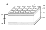
図4は、図1の光学素子10の適用例として、マイクロレンズアレイ100を示す模式図である。マイクロレンズアレイ100は、電極13の表面13sに複数の光散乱体15の配列を有する。
FIG. 4 is a schematic diagram showing a
マイクロレンズアレイ100は、一対の電極12と電極13の間に、高分子材料層11が挟持された三層の積層構造を有する。高分子材料層11は、図1を参照して説明したように、PC、ポリメタクリル酸メチル、ポリウレタン、ポリスチレン、ポリ酢酸ビニル、ポリビニルアルコール、ポリカーボネート、ポリエチレンテレフタレート、ポリアクリロニトリル、シリコーンゴム等のポリマーゲルである。
The
ポリマーゲルに、DBA、DEA、DES、DOP、DEP等の可塑剤を添加してもよい。可塑剤の混合比は、50wt%以上、より好ましくは75wt%以上である。 A plasticizer such as DBA, DEA, DES, DOP, DEP may be added to the polymer gel. The mixing ratio of the plasticizer is 50 wt% or more, more preferably 75 wt% or more.
電極12と電極13は、適切な導電性の材料で形成されている。電極12は陰極層、電極13は陽極層であり、光散乱体15の配列は、陽極の表面13sに形成されている。一例として、高分子材料層11の厚さは500μm、光散乱体15の径は150μm、中心心間のピッチは200μm、隣接する2つの光散乱体15の間隔は50μmである。
マイクロレンズアレイ100は、フィルム状の電極13に形成されたミクロンオーダーの開口とポリマーゲルの弾性を利用して形成されており、電極13の表面13sに、均一な凸形状の光散乱体15が配列されている。
The
図2を参照して説明したように、電極12と電極13の間に印加される電圧のレベルに応じて、光散乱体15の配列を出現させ、及び/または光散乱体15の高さを変更することができる。
As described with reference to FIG. 2, depending on the level of voltage applied between
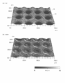
図5A及び図5Bは、図4のマイクロレンズアレイ100に印加する電圧のレベルを変えながら観察した3D画像である。印加電圧を0V、600V、700V、800Vと変化させて得られた各画像が図5Aの(A)、(B)、及び図5Bの(A),(B)である。電極13の表面13sの位置を0μmとして、光散乱体15が突出する方向をプラス側、表面13sよりも低い側をマイナス側とする。3D観測は、キーエンス社製のデジタルマイクロスコープVHX1000を用いて行う。
5A and 5B are 3D images observed while changing the voltage level applied to the
図6は、図5A及び図5Bの3D観察に用いたサンプルの電極3の諸元を説明する図である。電極13は、複数の開口14を有する。6mm×6mmの開口領域に、径φが150μmの開口14を30×30のマトリクスに配置する。開口14のピッチPは200μm、隣接する開口14と開口14の間隔は50μmである。
FIG. 6 is a diagram for explaining specifications of the
陰極となる電極12にITOフィルムを用い、陽極となる電極13に金属膜を用いる。電極12の厚さt1は30μm、電極13の厚さt2は30μm、高分子材料層11の厚さt3は500μmである。
An ITO film is used for the
高分子材料層11は、PVCにアジピン酸ジブチル(DBA)を混合比率が80wt%となるように添加し、THFの溶媒に完全に溶解させてゲル溶液とした後、ゲル溶液を電極12の上に厚さ500μmでキャストしたものである。可塑剤であるDBAはマイナスイオンを帯びやすく、電圧の印加により、ポリマーゲルを陽極の開口14に引き付けることができる。高分子材料層11の上に、電極13を配置する。
The
図5A及び図5Bに戻って、図5Aの画像(A)で電圧の印加がない場合は(V=0V)、高分子材料層11は開口14の内部でフラットな状態にある。同図の画像(B)で、600Vの電圧を印加すると、開口14内に部分的な突起が観察される。図5Bの画像(A)で、700Vの電圧を印加すると、ポリマーゲルが開口14の全体にわたって凸形状に変形して、電極13の表面から突出する。同図の画像(B)で、800Vの電圧を印加すると、さらに高さが増大して中心に対してほぼ対称の凸形状が得られる。
5A and 5B, when no voltage is applied (V=0V) in image (A) of FIG. 5A,
図7は、図5A及び図5Bの3D画像から、対角上に並ぶ3つの連続する光散乱体15の高さを電圧印加の関数としてプロットしたものである。縦軸が電極13の表面13sからの高さ、横軸が電極13の面内位置であり、1グリッドを150μmとしている。
FIG. 7 plots the height of three
電圧の印加がないとき(0V)、開口14の内部でのポリマーゲルの高さ位置は、-30μmよりも数μm浅い位置にある。これは電極3の自重により高分子材料層11の表面がわずかに開口14に中に入るからである。開口14内でのポリマーゲルのプロファイルは平坦になっている。
When no voltage is applied (0 V), the height position of the polymer gel inside the
電圧の印加が500Vのとき、ポリマーゲルの変形が始まり、開口14の中心近傍でポリマーゲルの表面位置が、初期位置よりも低くなる。これは、プラスの開口14のエッジがプラス極になり、ポリマーゲルが開口14の側壁に張り付いて引き上げられたことにより、開口の中央近傍でポリマーゲルの表面位置が下がったためである。
When a voltage of 500 V is applied, deformation of the polymer gel begins, and the surface position of the polymer gel near the center of the
電圧の印加が600Vのとき、ポリマーゲルは部分的に、開口14から電極13の表面位置を超えて突出する。突出は、開口14の中央部分から始まる。
When a voltage of 600 V is applied, the polymer gel partially protrudes from the
電圧の印加が700Vのとき、ポリマーゲルの突出が顕著になり、凸型に変形する。電圧の印加が800Vで、高さが40μmの凸形状が得られる。図7のプロファイルから分かるように、各光散乱体の端面形状は均一な形状となる。図4の構成を採用することで、電圧の印加により均一なマイクロレンズアレイが得られる。 When a voltage of 700 V is applied, the polymer gel protrudes significantly and deforms into a convex shape. A voltage of 800 V is applied to obtain a convex shape with a height of 40 μm. As can be seen from the profile in FIG. 7, the end face shape of each light scatterer is uniform. By adopting the configuration of FIG. 4, a uniform microlens array can be obtained by applying a voltage.
図8は、図5A及び図5Bの電圧印加によるマイクロレンズアレイの動作原理を説明する図である。図8(A)で、印加電圧が500V未満のときは、高分子材料層11は表面がフラットな状態で開口14の内部にある。このときの高分子材料層11の表面位置は、高さ方向(積層方向)で電極13の表面13sよりも低い。ここで、印加電圧が500V未満というのは、用いる高分子材料層11の弾性率、電極13の開口14の径φ等によって決まる電圧レベルであり、一例にすぎないことに留意されたい。
8A and 8B are diagrams for explaining the principle of operation of the microlens array by voltage application of FIGS. 5A and 5B. In FIG. 8A, when the applied voltage is less than 500 V, the
図8(B)のように、印加される電圧レベルを600Vとすることで、電子を帯びたポリマーゲルが陽極の電極13の開口14の端面に引き付けられる。ポリマーゲルの変形の初期は、プラスの電荷をおびている開口14の端面に優先的に引き付けられ、開口14の中央部でポリマーゲルは、電極13の表面13s位置よりも低い。図5A、図5B、及び図7を参照すると、ポリマーゲルが開口14の周囲に引き付けられた凹状態から凸状態に遷移するときの最初の突起は、開口14の中央部から生じると考えられる。
As shown in FIG. 8B, by applying a voltage level of 600 V, the electron-bearing polymer gel is attracted to the end surface of the
図8(C)で、印加される電圧レベルが600Vを超えると、ポリマーゲルの弾性により、ポリマーゲルは開口14内に全体的に押し上げられる。開口14で圧縮された分のポリマーゲルは開口14からさらに押し上げられ、電極13の表面13sから突出し、光散乱体15が形成される。
In FIG. 8(C), when the applied voltage level exceeds 600V, the elasticity of the polymer gel pushes it entirely up into the
なお800Vを印加してもポリマーゲルに流れる電流は10μA以下と非常に低く、発熱量が抑制され、長期の使用に耐えられる。 Even if 800 V is applied, the current flowing through the polymer gel is very low, ie, 10 μA or less.
図8のポリマーゲルの変化は、すべての開口14で発生する。高分子材料層11の組成が完全に均一、かつすべての開口14が完全に同一な理想的な状態では、均一な形状の光散乱体15のアレイが得られるはずである。実際は、開口14の加工ばらつき、高分子材料層11の内部での組成のばらつき等により、図7のように、光散乱体15の形状に若干のばらつきが含まれるが、図5Bで観察されるように、全体として均一なマイクロレンズアレイ100が実現される。
The change in polymer gel of FIG. 8 occurs at all
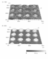
図9は、比較例として、電極13に替えて、断面が円形の金属配線を用いたメッシュ電極を用いたときのポリマーゲルの変化を観察した3D画像である。直径70μmの銅線を140μ間隔のメッシュに編み込んで、140μm×140μmの開口114を有するメッシュ電極を形成する。図5A及び図5Bで用いたのと同じ厚さ30μmの陰極の上に、同一組成のポリマーゲルを用いた高分子材料層11を厚さ150μmに塗布する。高分子材料層11の上にメッシュ電極を配置し、図5Bと同様に、陰極とメッシュ電極の間に800Vの電圧を印加する。3D観察では、800Vの電圧を印加してもメッシュ電極の開口114内に、突起が観察されない。
FIG. 9 is a 3D image obtained by observing a change in polymer gel when using a mesh electrode using metal wiring with a circular cross section instead of the
図10は、図9の3D画像から、X-X'ラインに沿って並ぶ開口内の高分子材料層11の高さをプロットしたものである。縦軸がメッシュ電極の表面からの高さである。メッシュ電極は、断面が円形の銅電線で形成されており、同電線の最も高い位置を0μmとしている。
FIG. 10 plots the height of the
図10からわかるように、800Vの電圧をかけても、メッシュ電極の開口114から表面に突出する突起は形成されない。これは、実施形態のマイクロレンズアレイ100に用いられる電極13が高分子材料層11と面接触しているのに対し、導電線を編み込んだメッシュ電極は、垂直断面で高分子材料層11と点接触に近い状態にあるからと考えられる。
As can be seen from FIG. 10, even if a voltage of 800 V is applied, projections protruding from the
なお、図10で電圧印加がない状態での高さ位置が-200μmになっているのは、メッシュ構造で導電線がクロスする点では、導電線が2本分の厚さになるからである。メッシュの編み込みは必ずしも均一でなく、導電線に隙間や歪みが含まれるとクロス位置での深さ位置は若干変動する。光学的な測定で光が入りづらい深さ方向での誤差(±20μm程度)を考慮すると、図10の測定結果は妥当な結果である。 The reason why the height position is −200 μm when no voltage is applied in FIG. 10 is that the conductive wire has a thickness of two at the point where the conductive wire crosses in the mesh structure. . The weaving of the mesh is not necessarily uniform, and if the conductive wire contains gaps or distortions, the depth position at the cross position will vary slightly. Considering the error (about ±20 μm) in the depth direction where light is difficult to enter in optical measurement, the measurement result of FIG. 10 is a reasonable result.
図11は、図9の比較例の構成で電圧が印加されたときの動作を説明する図である。図11(A)で印加電圧が0Vのときは、高分子材料層11の表面はフラットである。高分子材料層11の上に配置されるメッシュ電極の導電線は、接線方向で高分子材料層11の表面と接触している。
11A and 11B are diagrams for explaining the operation when a voltage is applied in the configuration of the comparative example shown in FIG. When the applied voltage is 0 V in FIG. 11A, the surface of the
図11(B)で800Vの電圧を印加した場合、負の電荷をおびたポリマーゲルは、陽極線(メッシュ電極)の周囲に張り付くように、流動する。しかし、開口114内でゲルが突起するほどの変形は生じない。陽極線と高分子材料層11の接触は点接触であり、ポリマーゲルを開口114内で均一に押し上げる変形をもたらすだけの均一な電圧印加が得られていないためと考えられる。
When a voltage of 800 V is applied in FIG. 11B, the negatively charged polymer gel flows so as to stick around the anode wire (mesh electrode). However, deformation to the extent that the gel protrudes within the
印加電圧をさらに高くした場合(たとえば1000V以上にした場合)は、開口114内にポリマーゲルが突出する可能性があり得るが、消費電力が大きくなるうえに、実施形態のような均一な形状の光散乱体15の配列を有するマイクロレンズアレイは期待できない。
If the applied voltage is further increased (for example, 1000 V or more), the polymer gel may protrude into the
図12は、光学素子10のさらに別の変形例として、光学素子10Bの構成を示す。図1~図3の構成では、電極13は開口14を有しており、電圧印加の下で光散乱体15を開口14から突出させている。図12の構成では、電極13は、所定の形状の非導電性領域19を有する。非導電性領域19は、電気的に中立で、かつ高分子材料層11の変形に追従して変形可能な光透過性の材料で形成されている。
FIG. 12 shows the configuration of an
変形可能な非導電性かつ光透過性の材料は、高分子材料層11と同じ材料であってもよいし、異なる材料であってもよい。非導電性領域19を高分子材料層11と異なる材料で形成する場合は、屈折率の違いを利用して、光の拡散を制御することができる。
The deformable non-conductive and light-transmissive material may be the same material as the
非導電性領域19の平面形状は、光学素子の目的、用途に応じて適宜選択され、円、楕円、多角形等である。非導電性領域19は、たとえば、電極13にあらかじめ所定の形状の開口14を形成し、開口内に、電気的に中立、かつ高分子材料層11の変形に追従して変形可能な光透過性の材料の層を充填することで形成される。
The planar shape of the
図12(B)に示すように、電極12と電極13の間に電圧が印加されると、高分子材料層11が変形する。高分子材料層11の変形に追従して非導電性領域19が変形する。高分子材料層11の変形部18と、非導電性領域19とで、光散乱体15が形成される。
As shown in FIG. 12B, when a voltage is applied between the
非導電性領域19を構成する層の厚さは、必ずしも電極13の厚さと一致している必要はなく、電極13の厚さよりも薄くてもよい。また、非導電性領域19と高分子材料層11はかならずしも面接触していなくてもよく、間に空気層が介在していてもよい。後者の場合、電圧の印加により高分子材料層11が変形して非導電性領域19と接触すると、高分子材料層11の変形に追従して非導電性領域19が変形して、光散乱体15を形成することができる。
The thickness of the layer forming the
図13は、実施形態の光学素子10の光拡散分布を評価するテスト装置の模式図である。光学素子10は、陽極に150μm径の開口が形成された厚さ30μmの金属フィルムを用い、陰極に、厚さ150μmのITOフィルムを用いている。陽極と陰極の間に挟まれる高分子材料層として、可塑剤DBAの含有率が83%のPVCゲルを用いる。PVCゲルの厚さは150μmである。この三層構造の光学素子10をポリエチレンテレフタレート(PET)のベースフィルム上に保持し、種々の直流電圧を印加して光散乱体15を陽極の表面に形成する。
FIG. 13 is a schematic diagram of a test device for evaluating the light diffusion distribution of the
光学素子10は、陰極となるITO膜がレーザ源の側にあり、光散乱体15がスクリーンの方向に向かって突出するように保持されている。電極に印加される電圧を、0V、600V、700V、800Vと変化させる。各電圧レベルで、レーザ源から赤色平行光Lを光学素子10に入射して、光散乱体15による集光と拡散を評価する。上述のように、赤色レーザ光は光学素子10の透明な陰極側から入射し、光散乱体15によって集光される。
The
光学素子10の光散乱体15の径は150μm、高さは0~40μmである。陽極の表面に光散乱体15が形成されて集光機能が発現した場合、その焦点位置は光学素子10のきわめて近傍にあり、肉眼での観察が困難である。そこで、焦点を超えた位置にスクリーンを配置し、一度集光した後の光拡散を観察する。
The
図14は、図13のテスト装置での評価結果を示す画像である。画像(A)は、印加電圧が0Vのときのスクリーン上の光拡散画像である。画像(B)は、印加電圧が600Vのときのスクリーン上の光拡散画像である。画像(C)は、印加電圧が700Vのときのスクリーン上の光拡散画像である。画像(D)は、印加電圧が800Vのときのスクリーン上の光拡散画像である。 FIG. 14 is an image showing the evaluation results of the test device of FIG. Image (A) is a light diffusion image on the screen when the applied voltage is 0V. Image (B) is a light diffusion image on the screen when the applied voltage is 600V. Image (C) is a light diffusion image on the screen when the applied voltage is 700V. Image (D) is a light diffusion image on the screen when the applied voltage is 800V.
図14の(A)で、電圧が印加されていないときは、光学素子10の陽極面に光散乱体15は形成されておらず、陰極のITOフィルムから入射した光は、フラットなPVCゲル層をそのまま透過して、スクリーンに投射される。光の拡散は小さく、スクリーンの中央に明るいスポットが観察される。
In FIG. 14A, when no voltage is applied, the
図14の(B)で、印加電圧が600Vのときは、PVCゲルの変形初期であり、変形が開始されても集光機能を発現する凸形状には至っていない。したがって、光学素子10の陰極側から入射した光は、集光作用をほとんど受けずにスクリーンに投射され、印加電圧が0Vのときと類似した光スポットが観察される。
In (B) of FIG. 14, when the applied voltage is 600 V, the PVC gel is in the initial stage of deformation, and even if the deformation starts, it has not yet reached a convex shape that exhibits the light collecting function. Therefore, the light incident from the cathode side of the
図14の(C)で、印加電圧が700Vのときは、陽極の表面に凸状の光散乱体15が形成される。レーザ光は光散乱体15で集光された後に拡散して、拡散光がスクリーンに投射される。700Vの電圧印加では、光散乱体15の曲率半径は比較的大きく、焦点距離が長いため、スクリーン位置での光の拡散はそれほど顕著ではない。
In FIG. 14C, when the applied voltage is 700 V, convex
図14の(D)で、印加電圧が800Vのときは、陽極の表面により高さの高い凸状の光散乱体15が形成される。光散乱体の曲率半径は小さく、焦点距離が短くなり、光学素子10の近傍で焦点を結んだあとに拡散される。スクリーンの位置では、大きく拡散された光が観察される。
In (D) of FIG. 14, when the applied voltage is 800 V, a taller convex
これらの光拡散分布から、印加電圧を調整することにより、光散乱体15の焦点距離を可変にできることが確認される。実施形態の光学素子10は、可変焦点レンズ、または可変形状レンズとして用いることができる。
From these light diffusion distributions, it is confirmed that the focal length of the
図15は、実施形態のマイクロレンズアレイ100を用いた撮像装置150の模式図である。撮像装置150は、複数の光散乱体15の配列を有するマイクロレンズアレイ100と、複数の撮像素子が配列された撮像素子アレイ130を有する。撮像素子は、CCD(charge coupled device)、CMOS(complementary metal oxide semiconductor)センサなどで形成されている。撮像素子の配列に対応して、三色のカラーフィルタ131が配置されていてもよい。この例では、赤(R)、緑(G)、青(B)のカラーフィルタ131R、131G、131Bが交互に配置されている。
FIG. 15 is a schematic diagram of an
図16は、実施形態のマイクロレンズアレイ100を用いた照明装置250の模式図である。照明装置250は、たとえばLEDランプ等の光源230と、光源230の出力側の前面に配置されたマイクロレンズアレイ100を有する。マイクロレンズアレイ100を配置することで、光拡散を制御して、輝度を高く保った状態で拡散光を平行光に変換することができる。また、微細な発光素子の出力面の近傍に実施形態の光学素子、または複数個の光散乱体15を有するマイクロレンズアレイ100を配置することで、顕微鏡用、産業用等の照明装置に適用することもできる。
FIG. 16 is a schematic diagram of an
マイクロレンズアレイ100は、1mm以下の薄型に形成され、陽極、陰極ともに透明化することができるので、超薄型カメラ、ヘッドマウントディスプレイ(HMD)、マイクロレンズアレイ(MLA)シート、等への適用のほか、内視鏡システム等の医療の分野にも適用可能である。単一の光散乱体15を有する光学素子10も、医療、画像形成の分野で光拡散シート、レンズシート等に適用することができる。
Since the
<高分子材料の構成>
上述のように、実施形態の光学素子とマイクロレンズアレイは、複雑な機構を用いずに電圧をオン/オフ制御、あるいは電圧レベルを調整することで、様々な配向分布をもつ光散乱体を発生させることができる。印加される電圧は低い方が望ましい。そこで、光学素子及びマイクロレンズアレイに用いられる高分子材料の組成を工夫して、印加電圧を低減する。
<Structure of polymer material>
As described above, the optical element and microlens array of the embodiment generate light scatterers with various orientation distributions by controlling the voltage on/off or adjusting the voltage level without using a complicated mechanism. can be made A lower voltage is desirable. Therefore, the applied voltage is reduced by devising the composition of the polymer material used for the optical element and the microlens array.
具体的には、高分子材料層11で用いられるゲル状の高分子材料(ポリマーゲル)に、所定の条件を満たすイオン液体を添加することで、光学素子10またはマイクロレンズアレイ100の駆動電圧を低減する。イオン液体の添加により、高分子材料の変形効率を高めることができる。
Specifically, by adding an ionic liquid that satisfies a predetermined condition to the gel-like polymer material (polymer gel) used in the
イオン液体は、カチオン(正の電荷を帯びたイオン)とアニオン(負の電荷を帯びたイオン)で構成される塩であり、25℃で液体のものをいう。所定の条件のひとつは、イオン液体が、25℃で一定値以上のアニオン(負イオン)輸率をもつことである。この条件の詳細については、後述する。 An ionic liquid is a salt composed of cations (positively charged ions) and anions (negatively charged ions) and is liquid at 25°C. One of the predetermined conditions is that the ionic liquid has an anion (negative ion) transport number equal to or higher than a certain value at 25°C. The details of this condition will be described later.
高分子材料は、上述したように、ポリ塩化ビニル(PVC:polyvinyl chloride)、ポリメタクリル酸メチル、ポリウレタン、ポリスチレン、ポリ酢酸ビニル、ポリビニルアルコール、ポリカーボネート、ポリエチレンテレフタレート、ポリアクリロニトリル、シリコーンゴム等である。好ましい構成例では、使用波長に対して透明な高分子または樹脂材料が用いられる。 Polymer materials include polyvinyl chloride (PVC), polymethyl methacrylate, polyurethane, polystyrene, polyvinyl acetate, polyvinyl alcohol, polycarbonate, polyethylene terephthalate, polyacrylonitrile, silicone rubber, etc., as described above. In a preferred configuration example, a polymer or resin material transparent to the wavelengths used is used.
このような高分子材料に対するイオン液体の重量割合は、0.2 wt%以上、1.5 wt%以下であり、より好ましくは、0.3 wt%以上、1.0 wt%以下である。高分子材料の重量を1(または100%)としたときに、この重量割合のイオン液体を混合することで、光学素子またはマイクロレンズアレイの駆動電圧を低減することができる。この根拠についても後述する。 The weight ratio of the ionic liquid to such a polymer material is 0.2 wt% or more and 1.5 wt% or less, more preferably 0.3 wt% or more and 1.0 wt% or less. Assuming that the weight of the polymer material is 1 (or 100%), the driving voltage of the optical element or microlens array can be reduced by mixing the ionic liquid in this weight ratio. The grounds for this will also be described later.
ポリマーゲルに適切な可塑剤を添加してもよいし、溶媒に溶解させてもよい。可塑剤を用いる場合は、アジピン酸ジブチル(DBA:dibutyl adipate)、アジピン酸ジエチル(DEA:diethyl adipate)、セバシン酸ジエチル(DES:diethyl sebacate)、フタル酸ジオクチル(DOP:dioctyl phthalate)、フタル酸ジエチル(DEP:diethyl phthalate)等を用いることができる。溶媒としては、テトラヒドロフラン(THF)等のエーテル系の溶媒を用いることができる。 A suitable plasticizer may be added to the polymer gel or dissolved in the solvent. When using a plasticizer, dibutyl adipate (DBA), diethyl adipate (DEA), diethyl sebacate (DES), dioctyl phthalate (DOP), diethyl phthalate (DEP: diethyl phthalate) or the like can be used. As a solvent, an ether solvent such as tetrahydrofuran (THF) can be used.
イオン液体が添加された高分子材料は、図1及び図2の光学素子10、図3の光学素子10A、図12の光学素子10B、及び図4のマイクロレンズアレイ100のいずれにも適用可能である。以下で詳細に述べるように、高分子材料に所定の条件のイオン液体を添加することで、高分子材料層11の駆動電圧を200V以下、より好ましくは、150V以下に低減することができる。
The polymer material to which the ionic liquid is added can be applied to any of the
図17は、種々のイオン液体を添加したときのポリマーゲルの電圧応答特性を示す。重量平均分子量が230000のPVCをテトラヒドロフラン(THF)の溶媒に溶解させたポリマーゲルを準備し、種々のイオン液体を添加して複数種類のサンプルを作製する。各サンプルを図1及び図2のように電極12と電極13の間に挟み込み、印加電圧を変えてピーク高さhの電圧依存性を測定する。比較例として、イオン液体が添加されていないポリマーゲルを用いて、同じくピーク高さの電圧依存性を測定する。ここで、ピーク高さというときは、電極13の表面13sからの高さhが最も高い部分の値をいう。
FIG. 17 shows voltage response characteristics of polymer gels when various ionic liquids are added. A polymer gel is prepared by dissolving PVC having a weight-average molecular weight of 230,000 in a tetrahydrofuran (THF) solvent, and various ionic liquids are added to prepare a plurality of types of samples. Each sample is sandwiched between the
下部電極となる電極12の上に、サンプルと比較例のポリマーゲルを厚さ300μmに塗布する。ポリマーゲルの上に、上部の電極13として、直径100μmのホールが形成された厚さ20μmの金属薄膜を配置する。電極12と電極13の間に印加する電圧を0Vから400Vの間で変化させて、電極13から突出する光散乱体15のピーク高さhを測定する。
The polymer gels of the sample and the comparative example are applied to a thickness of 300 μm on the
ラインAは、イオン液体として1-エチル-3-メチルイミダゾリウム=テトラフルオロボラート(EMI-BF4)を添加したサンプルAのピーク高さの電圧依存性を示す。PVCに対するEMI-BF4の重量割合は0.5 wt%であ。EMIはカチオン、BF4はアニオンである。 Line A shows the voltage dependence of the peak height of sample A to which 1-ethyl-3-methylimidazolium tetrafluoroborate (EMI-BF 4 ) was added as an ionic liquid. The weight ratio of EMI-BF 4 to PVC is 0.5 wt%. EMI is a cation and BF4 is an anion.
ラインBは、イオン液体として1-オクチル-3-メチルイミダゾリウム=テトラフルオロボラート(OMI-BF4)を添加したサンプルBのピーク高さの電圧依存性を示す。PVCに対するOMI-BF4の重量割合は0.5 wt%である。OMIはカチオン、BF4はアニオンである。 Line B shows the voltage dependence of the peak height of sample B to which 1-octyl-3-methylimidazolium tetrafluoroborate (OMI-BF 4 ) was added as an ionic liquid. The weight ratio of OMI-BF 4 to PVC is 0.5 wt%. OMI is a cation and BF4 is an anion.
ラインCは、イオン液体として1-エチル-3-メチルイミダゾリウム=ジシアナミド(EMI-DCA)を添加したサンプルCのピーク高さの電圧依存性を示す。PVCに対するEMI-DCAの重量割合は、0.5 wt%である。EMIはカチオン、DCA(C2N3)はアニオンである。 Line C shows the voltage dependence of the peak height of sample C to which 1-ethyl-3-methylimidazolium=dicyanamide (EMI-DCA) was added as an ionic liquid. The weight ratio of EMI-DCA to PVC is 0.5 wt%. EMI is a cation and DCA(C 2 N 3 ) is an anion.
ラインDは、イオン液体としてテトラブチルホスホニウム=テトラフルオロボラート(TBP-BF4)を添加したサンプルDのピーク高さの電圧依存性を示す。PVCに対するTBP-BF4の重量割合は、0.1 wt%である。TBPはカチオン、BF4はアニオンである。 Line D shows the voltage dependence of the peak height of sample D to which tetrabutylphosphonium=tetrafluoroborate (TBP-BF 4 ) was added as an ionic liquid. The weight ratio of TBP-BF 4 to PVC is 0.1 wt%. TBP is a cation and BF4 is an anion.
ラインEは、イオン液体としてテトラブチルホスホニウム=テトラフルオロボラート(TBP-BF4)を添加したサンプルEのピーク高さの電圧依存性を示す。イオン液体の種類はサンプルDと同じであるが、PVCに対するTBP-BF4の重量割合は0.5 wt%である。TBPはカチオン、BF4はアニオンである。 Line E shows the voltage dependence of the peak height of sample E to which tetrabutylphosphonium=tetrafluoroborate (TBP-BF 4 ) was added as an ionic liquid. The type of ionic liquid is the same as sample D, but the weight ratio of TBP-BF 4 to PVC is 0.5 wt%. TBP is a cation and BF4 is an anion.
ラインFは、イオン液体として1-エチル-3-メチルイミダゾリウム=トリフルオロメタンスルフォンイミド(EMI-TFSI)を添加したサンプルFのピーク高さの電圧依存性を示す。PVCに対するEMI-TFSIの重量割合は0.5 wt%である。EMIはカチオン、TFSIはアニオンである。 Line F shows the voltage dependence of the peak height of sample F to which 1-ethyl-3-methylimidazolium=trifluoromethanesulfonimide (EMI-TFSI) was added as an ionic liquid. The weight ratio of EMI-TFSI to PVC is 0.5 wt%. EMI is a cation and TFSI is an anion.
ラインGは、イオン液体としてテトラブチルホスホニウム=メタンスルホン酸(TBP-MES)を添加したサンプルGのピーク高さの電圧依存性を示す。PVCに対するTBP-MESの重量割合は、0.5 wt%である。TBPはカチオン、MESはアニオンである。 Line G shows the voltage dependence of the peak height of sample G to which tetrabutylphosphonium=methanesulfonic acid (TBP-MES) was added as an ionic liquid. The weight ratio of TBP-MES to PVC is 0.5 wt%. TBP is a cation and MES is an anion.
ラインWは、比較例としてイオン液体が添加されていないサンプルWのPVCポリマーゲルのピーク高さの電圧依存性を示す。 Line W indicates the voltage dependence of the peak height of the PVC polymer gel of sample W to which no ionic liquid was added as a comparative example.
図17の測定結果から、イオン液体を添加しない場合でも、誘電分極が生じるポリマーゲルを用いることで、電圧印加によりポリマーゲルが変形する。イオン液体を添加していない比較例のポリマーゲルWでは、印加電圧に対してほぼリニアに光散乱体15の高さが増大している。しかし、サンプルWを電極13の表面13sから20μmの高さに突出させるには、400Vの電圧が必要である。
From the measurement results of FIG. 17, even when no ionic liquid is added, the polymer gel is deformed by voltage application by using a polymer gel in which dielectric polarization occurs. In the polymer gel W of the comparative example to which no ionic liquid is added, the height of the
これに対し、イオン液体としてEMI-BF4を0.5 wt%添加したサンプルAと、OMI-BF4を0.5 wt%添加したサンプルBは、100V以下の電圧印加で、高分子材料層11を20μm以上の高さに駆動することができる。特に、サンプルAは、50Vの電圧印加で20μmの高さ、200Vの電圧印加で、40μm弱の高さに変位する。サンプルBも、100Vの電圧印加で25μmの高さ、200Vの電圧印加で30μmの高さに変位する。 On the other hand, in sample A to which 0.5 wt% of EMI-BF 4 was added as an ionic liquid and sample B to which 0.5 wt% of OMI-BF 4 was added, a voltage of 100 V or less was applied to the polymer material layer. 11 can be driven to a height of 20 μm or more. In particular, sample A displaces to a height of 20 μm when a voltage of 50 V is applied and to a height of slightly less than 40 μm when a voltage of 200 V is applied. Sample B is also displaced to a height of 25 μm when a voltage of 100 V is applied and to a height of 30 μm when a voltage of 200 V is applied.
EMI-DCAを0.5 wt%添加したサンプルCは、イオン液体を添加しないサンプルWと比較して、約半分の印加電圧(210~220V)で同じ20μmのピーク高さを得ることができ、変形効率を大きく向上している。 Sample C to which 0.5 wt% of EMI-DCA is added can obtain the same peak height of 20 μm at about half the applied voltage (210 to 220 V) as compared to Sample W to which no ionic liquid is added. Greatly improves transformation efficiency.
TBP-BF4を0.1 wt%添加したサンプルDは、50Vの電圧印加で電極13の表面13sから光散乱体15を突出させることができるが、電圧を高くしても、ピーク高さは10μm未満のままであり、50Vから400Vの範囲でピーク高さの変化が小さい。サンプルDでは、電圧制御により光散乱体15の高さを精度良く調整することが難しい。
Sample D, to which 0.1 wt% of TBP-BF 4 was added, can cause the
TBP-BF4を0.5 wt%添加したサンプルE、EMI-TFSIを0.5 wt%添加したサンプルF、及びTBP-MESを0.5 wt%添加したサンプルGは、400Vの電圧を印加しても、電極13の表面13sから光散乱体15を突出させることができない。
A voltage of 400 V was applied to sample E to which 0.5 wt% of TBP-BF 4 was added, sample F to which 0.5 wt% of EMI-TFSI was added, and sample G to which 0.5 wt% of TBP-MES was added. However, the
図17の測定結果から、イオン液体の種類(すなわち物性)と添加量の少なくとも一方が高分子材料層11の駆動電圧の低減に関与していると考えられる。
From the measurement results of FIG. 17, it is considered that at least one of the type (that is, physical properties) and the amount of addition of the ionic liquid is involved in the reduction of the driving voltage of the
<ポリマーゲルの変位とイオン液体の物性の関係>
図18は、ポリマーゲルの変位とイオン液体の物性の関係を示す図である。イオン液体として、図17のサンプルA~Gに加えて、1-エチル-3-メチルイミダゾリウム=フルオロスルホニルイミド(EMI-FSI)を添加したサンプルHの物性も併せて測定する。
<Relationship between displacement of polymer gel and physical properties of ionic liquid>
FIG. 18 is a diagram showing the relationship between the displacement of the polymer gel and the physical properties of the ionic liquid. In addition to samples A to G in FIG. 17, the physical properties of sample H added with 1-ethyl-3-methylimidazolium=fluorosulfonylimide (EMI-FSI) as an ionic liquid are also measured.
各種のイオン液体を添加したサンプルA~Hで、変位がプラスのものは、電圧の印加によりポリマーゲルが電極13の表面13sから突出して光散乱体15が形成されたものを示す。変位がマイナスのものは、電圧を印加しても電極13の表面13sからポリマーゲルが突出しないものである。
Among the samples A to H to which various ionic liquids were added, positive displacement indicates that the polymer gel protrudes from the
各イオン液体の物性として、導電率、電位窓のサイズ、25℃での負イオンの拡散係数と輸率を測定する。用いたイオン液体の中には、25℃で固体のものもあるため、80℃に加熱して溶融したものについては、80℃での負イオンの拡散係数と輸率を測定する。 As the physical properties of each ionic liquid, the electrical conductivity, the size of the potential window, the diffusion coefficient of negative ions at 25° C. and the transport number are measured. Since some of the ionic liquids used are solid at 25°C, the diffusion coefficient and transference number of negative ions at 80°C are measured for those that are melted by heating to 80°C.
上述のパラメータのうち、まず導電率について検討する。サンプルCは、サンプルA,Bと比較して導電率が2桁小さいが、サンプルCを添加したポリマーゲルはプラスに変位している。これに対し、サンプルHは、サンプルCよりもはるかに導電率が大きいが、ポリマーゲルはプラスに変位していない。イオン液体の導電率は、ポリマーゲルの変形効率に直接関係しないと考えられる。 Among the above parameters, the conductivity will be considered first. The conductivity of sample C is two orders of magnitude lower than that of samples A and B, but the polymer gel to which sample C is added has a positive displacement. In contrast, sample H is much more conductive than sample C, but the polymer gel is not positively displaced. It is believed that the conductivity of the ionic liquid is not directly related to the deformation efficiency of the polymer gel.
電位窓は、図2の系で電気化学的に安定性が保たれる電位領域のことである。電位窓が広いほど(数値が大きいほど)、系が電気化学的に安定する範囲が広い。サンプルAとサンプルFの電位窓は同じ広さであるにもかかわらず、サンプルAのポリマーゲルはプラスに変位し、サンプルFのポリマーゲルは、プラスの変位が得られていない。イオン液体の電位窓の広さも、ポリマーゲルの変形効率に直接関係しないと考えられる。 A potential window is a potential region in which electrochemical stability is maintained in the system of FIG. The wider the potential window (the larger the number), the wider the range in which the system is electrochemically stable. Although the potential windows of sample A and sample F are the same width, the polymer gel of sample A is positively displaced, and the polymer gel of sample F is not positively displaced. The width of the potential window of the ionic liquid is also not directly related to the deformation efficiency of the polymer gel.
次に、25℃でのアニオン(負イオン)の拡散係数と輸率について検討する。イオン液体に含まれる正負イオンの拡散係数は、測定機器として、固体NMR(Varian社製のVNMR System)を用いて測定する。測定手順は、キャピラリーにイオン液体を注入し、装置にセットする。所定温度(この場合は25℃と80℃)で磁場の変化に対するシグナル強度を計測し、Stokes-Einsteinの式から正負イオンの拡散係数を算出する。 Next, the diffusion coefficient and transference number of anions (negative ions) at 25° C. will be examined. The diffusion coefficient of positive and negative ions contained in the ionic liquid is measured using a solid NMR (VNMR System manufactured by Varian) as a measuring instrument. The measurement procedure is to inject the ionic liquid into the capillary and set it in the device. The signal intensity is measured with respect to changes in the magnetic field at predetermined temperatures (25° C. and 80° C. in this case), and the diffusion coefficients of positive and negative ions are calculated from the Stokes-Einstein equation.
負イオンの輸率は、イオン液体に電流を流した際に、全電流に対するアニオンが担う電流の割合を表わす。負イオンの輸率は、上記で求めた負イオンの拡散係数と正イオンの拡散係数の総和に対する負イオンの拡散係数の比(Danion/(Dcation+Danion))として計算される。 The transference number of negative ions represents the ratio of current carried by anions to the total current when a current is passed through an ionic liquid. The transference number of negative ions is calculated as the ratio of the diffusion coefficient of negative ions to the sum of the diffusion coefficients of negative ions and positive ions obtained above (D anion /(D cation +D anion )).
サンプルA、B、C、F、Hに用いられたイオン液体は、25℃で液体であり、液体クロマトグラフィーによる測定結果から、各イオン液体の負イオンの拡散係数と輸率を算出した。プラスの変位が得られたサンプルA、B,Cで、25℃でのイオン液体の負イオンの輸率は、いずれも0.4以上である。これに対し、プラスの変位が得られないサンプルFとHで用いられたイオン液体の25℃での負イオンの輸率は0.4よりも小さい。ここから、室温での負イオンの輸率がポリマーゲルの変形効率に影響していると考えられる。 The ionic liquids used for samples A, B, C, F, and H were liquid at 25° C., and the diffusion coefficient and transference number of negative ions of each ionic liquid were calculated from the measurement results by liquid chromatography. In samples A, B, and C in which positive displacement was obtained, the transference numbers of negative ions of the ionic liquids at 25° C. are all 0.4 or more. In contrast, the negative ion transference numbers at 25° C. of the ionic liquids used in samples F and H, which do not yield positive displacements, are less than 0.4. This suggests that the transference number of negative ions at room temperature affects the deformation efficiency of polymer gels.
なお、プラスの変位が得られたサンプルDに添加されたイオン液体TBP-BF4は、用いた液体クロマトグラフの加熱可能温度(80℃)では溶融しないため、拡散係数を測定することができなかった。 The ionic liquid TBP-BF 4 added to sample D, which gave a positive displacement, did not melt at the heatable temperature (80°C) of the liquid chromatograph used, so the diffusion coefficient could not be measured. rice field.
プラスの変位が得られないサンプルGに添加されたイオン液体TBP-MESも25℃で固体であるため、拡散係数を測定することができない。このイオン液体を80℃に加熱したところ、溶融したので負イオンの拡散係数と輸率を計算したところ、輸率は0.6であった。 The ionic liquid TBP-MES added to sample G, which does not give a positive displacement, is also solid at 25° C., so the diffusion coefficient cannot be measured. When this ionic liquid was heated to 80° C., it melted. When the diffusion coefficient and transference number of negative ions were calculated, the transference number was 0.6.
図18の結果から、高分子材料層11に添加されるイオン液体の特性として、25℃での負イオンの輸率が0.4以上のものが望ましいとわかる。
From the results of FIG. 18, it can be seen that the ionic liquid added to the
図17及び図18から、イオン液体のアニオンのサイズ(分子量)が小さいほうが、ポリマーゲルの変形効率に寄与することが推定される。一方、イオン液体のカチオンのサイズは、変形効率にはそれほど寄与していないと考えられる。しかし、サンプルDの変形効率が十分でないことから、カチオンの種類によって、陰極の劣化に影響している可能性がある。これについては、図21を参照して後述する。 From FIGS. 17 and 18, it is estimated that a smaller size (molecular weight) of the anion of the ionic liquid contributes to the deformation efficiency of the polymer gel. On the other hand, it is considered that the size of the cations in the ionic liquid does not significantly contribute to the deformation efficiency. However, since the deformation efficiency of sample D is not sufficient, it is possible that the type of cation affects the deterioration of the cathode. This will be described later with reference to FIG.
なお、サンプルGで用いられたイオン液体のアニオンサイズもカチオンサイズも中程度であるが、イオン液体が25℃で固体であるため、攪拌によってポリマーゲル中に分散されても、ゲルの変形効率にはそれほど寄与していないものと考えられる。 The anion size and cation size of the ionic liquid used in sample G are medium, but since the ionic liquid is solid at 25°C, even if it is dispersed in the polymer gel by stirring, the gel deformation efficiency will be may not contribute much.
以上から、BF4 ―及びDCA以外にも、アニオンとしてイオンサイズが比較的小さいCl-やBr―を用いることができる。また、カチオンとして、陰極の劣化に影響しないものを選択することで、種々のイオン液体を用いることができる。たとえば、Li-BF4 ―をイオン液体として用い得る。 From the above, it is possible to use Cl - and Br - , which have relatively small ion sizes, as anions other than BF 4 - and DCA. Various ionic liquids can be used by selecting cations that do not affect the deterioration of the cathode. For example, Li--BF 4 -- can be used as the ionic liquid.
<イオン液体の添加量とポリマーゲルの変位の関係>
図19は、イオン液体の添加量とポリマーゲルの変位の関係を示す図である。横軸は、ポリマーゲルの高分子材料に対するイオン液体の含有量(wt%)、縦軸が変位のピーク高さである。
<Relationship between amount of ionic liquid added and displacement of polymer gel>
FIG. 19 is a diagram showing the relationship between the amount of ionic liquid added and the displacement of the polymer gel. The horizontal axis is the content (wt%) of the ionic liquid with respect to the polymeric material of the polymer gel, and the vertical axis is the displacement peak height.
高分子材料として、分子量が230000のPVCを用い、イオン液体としてサンプルAのEMI-BF4を用いる。EMI-BF4の添加量を0 wt%から5.0 wt%の範囲で変化させる。また、印加電圧を0V、50V、100V、200V、400Vと変える。 PVC having a molecular weight of 230,000 is used as the polymer material, and EMI-BF 4 of sample A is used as the ionic liquid. The amount of EMI-BF 4 added is varied in the range of 0 wt% to 5.0 wt%. Also, the applied voltage is changed to 0V, 50V, 100V, 200V, and 400V.
印加する電圧のレベルに拠らず、イオン液体の添加量が、0.2 wt%~1.5 wt%の範囲でプラスの変位が得られる。また、0.3 wt%~1.0 wt%の範囲で、変位が最大になる。この範囲のイオン液体の添加により、100V以下の電圧印加で、電極13の表面に光散乱体15を形成することができる。イオン液体の添加量が5.0 wt%のときは、電圧をオフにしても変形が戻らないメモリー現象が発生する。
Regardless of the applied voltage level, a positive displacement is obtained in the range of 0.2 wt % to 1.5 wt % of the ionic liquid addition amount. Moreover, the displacement becomes maximum in the range of 0.3 wt% to 1.0 wt%. By adding the ionic liquid in this range, the
図19から、高分子に対するイオン液体の重量比率は、0.2 wt%~1.5 wt%が望ましく、より好ましくは、0.3 wt%~1.0 wt%であることがわかる。これは、図17の結果とも一致する。 From FIG. 19, it can be seen that the weight ratio of the ionic liquid to the polymer is desirably 0.2 wt% to 1.5 wt%, more preferably 0.3 wt% to 1.0 wt%. This agrees with the results of FIG. 17 as well.
図20は、高分子材料層11への電圧印加により形成される光散乱体15の光拡散分布の評価結果を、イオン液体の添加量ごとに示す図である。イオン液体としてEMI-BF4を用い、EMI-BF4の添加量を変えた高分子材料層11で、図2の光学素子10を作製する。高分子材料層11は、ポリマーゲルとしてPVCを含み、可塑剤としてアジピン酸ジブチル(DBA)を含む。PVCとDBAの総量に対するDBAの含有割合は83 wt%である。
FIG. 20 is a diagram showing evaluation results of the light diffusion distribution of the
陰極となる電極12を、厚さ150μmのITOで形成し、電極12と電極13の間に挟んだ高分子材料層11に電圧を印加して光散乱体15を形成する。図13と同様に、ITOで形成される電極12の側にレーザを配置し、光散乱体15が形成される側にスクリーンを配置する。電極12の裏面側から、赤色平行光のレーザ光を光学素子10に入射して、スクリーンでの光拡散状態を観察する。
The
スクリーンは、光散乱体15の光出射側で、光散乱体15の焦点よりも遠い位置に配置されている。光散乱体15の焦点で一度集光された後の光拡散を、スクリーン上で観察する。光学素子10の光散乱体15の径は100μm、高さは0~40μm程度と小さく、その焦点位置は光学素子10のきわめて近傍にあり、肉眼での観察が困難だからである。光散乱体15の焦点を超えた位置での光拡散を観察することで、集光状態を評価することができる。
The screen is arranged on the light exit side of the
イオン液体が添加されていないサンプル(「w/o IL」と表記)では、200Vの電圧を印加しても電極13の表面から突出する光散乱体15が形成されない。光学素子10の裏面から入射された赤色平行光は、集光されずに平行光のまま光学素子10を透過し、印加電圧のレベルにかかわらず、スクリーン上に同じサイズのスポットが形成されている。
In the sample to which no ionic liquid was added (denoted as “w/o IL”), the
EMI-BF4が0.05 wt%添加されたサンプルでは、100Vの電圧印加により、電極13の表面でポリマーゲルがわずかに膨らむが、集光機能が不十分であり、スクリーン位置でほぼ平行光のスポットが維持されている。200Vの電圧印加で、ピーク高さが10μm程度の(曲率の緩やかな)光散乱体15が形成される。いったん光散乱体15の焦点位置で集光された光は、拡散して広がり、スクリーン上にスポットは現れない。
In the sample to which 0.05 wt% of EMI-BF 4 was added, the polymer gel slightly swelled on the surface of the
EMI-BF4が0.5 wt%添加されたサンプルでは、50Vの電圧印加により、電極13の表面に光散乱体15が形成され、集光後に拡散し始めた光がスクリーン位置で観察される。100Vの電圧と200Vの電圧印加では、50V印加時よりもピーク高さが大きい、すなわち曲率が急な光散乱体15が電極13の表面に形成される。光学素子の裏側から入射した光は、集光された後に大きく拡散し、スクリーン位置でスポットは観察されない。これらの評価結果は、図19の測定結果と一致する。
In the sample to which 0.5 wt% of EMI-BF 4 was added,
図20の光拡散分布から、印加電圧を調整することにより、光散乱体15の焦点距離を可変にできることが確認される。実施形態の光学素子10は、可変焦点レンズ、または可変形状レンズとして用いることができる。
From the light diffusion distribution in FIG. 20, it is confirmed that the focal length of the
<イオン液体(カチオン)の陰極劣化への影響>
図21は、イオン液体の陰極劣化への影響を示す図である。試験用のサンプルとして、金属基板上に、種々のイオン液体を添加したPVCゲルを塗布し、PVCゲルの上に対向電極としてITO電極を配置する。
<Effect of ionic liquid (cation) on cathode deterioration>
FIG. 21 is a diagram showing the influence of ionic liquid on cathode deterioration. As test samples, PVC gels containing various ionic liquids are applied to a metal substrate, and an ITO electrode is placed on the PVC gel as a counter electrode.
塗布するPVCゲルの種類は、サンプルA(0.5 wt%のEMI-BF4を含む)、サンプルB(0.5 wt%のOMI-BF4を含む)、サンプルC(0.5 wt%のEMI-DCAを含む)、サンプルD(0.1 wt%のTBP-BF4を含む)、サンプルH(0.5 wt%のEMI-FSIを含む)、及びサンプルG(0.5 wt%のTBP-MESを含む)の6種類である。このうち、図18でプラスの変位が得られたのは、サンプルA~Dである。サンプルDは、イオン液体の重量割合を他のサンプルと同じ0.5wt%にした場合、変位が得られないので、添加量を0.1 wt%に減らしたサンプルである。 The types of PVC gel to be applied are sample A (containing 0.5 wt% EMI- BF4 ), sample B (containing 0.5 wt% OMI- BF4 ), sample C (containing 0.5 wt% EMI-DCA), Sample D (containing 0.1 wt% TBP- BF4 ), Sample H (containing 0.5 wt% EMI-FSI), and Sample G (containing 0.5 wt% including TBP-MES). Among them, positive displacement was obtained in samples A to D in FIG. Sample D is a sample in which the amount added is reduced to 0.1 wt% because displacement cannot be obtained when the weight ratio of the ionic liquid is 0.5 wt%, which is the same as in the other samples.
金属基板を正極、ITOを負極として、PVCゲルに印加する電圧レベルを変えながらITO側から電極の表面状態を観察する。 Using the metal substrate as the positive electrode and the ITO as the negative electrode, the surface state of the electrodes is observed from the ITO side while changing the voltage level applied to the PVC gel.
変位効果がなかったサンプルGは、50Vという低い印加電圧でITO(陰極)の劣化が観察される。また、サンプルDでも電圧印加によるITO電極の劣化が観察される。これは、カチオンがITO電極の劣化に影響しているためと考えられる。これに対し、変位効果の高いサンプルA~Cでは、印加電圧を上げてもITO電極の劣化は観察されていない。 In sample G, which had no displacement effect, deterioration of ITO (cathode) was observed at an applied voltage as low as 50V. Further, deterioration of the ITO electrode due to voltage application is observed in sample D as well. This is probably because cations affect the deterioration of the ITO electrode. On the other hand, in samples A to C having a high displacement effect, deterioration of the ITO electrode was not observed even when the applied voltage was increased.
図17~図21の考察から、25℃で負イオンの輸率が0.4以上のイオン液体を添加することで、イオン液体を添加しないポリマーゲルと比較して、低い印加電圧で大きな変形を得ることができる。特に、サンプルAとサンプルBのように、アニオンサイズが小さいイオン液体を用いると、100V以下の電圧範囲で、ピーク高さを大きく変えることができ、光散乱体15の制御が容易である。すなわち、印加電圧のレベルに応じて、光散乱体15を出現させ、その高さを調整することができる。これらのサンプルでは、光学素子10の駆動時に、陰極に対する悪影響も少ない。
From the consideration of FIGS. 17 to 21, by adding an ionic liquid having a negative ion transference number of 0.4 or more at 25° C., compared to a polymer gel to which no ionic liquid is added, a large deformation can be achieved at a low applied voltage. Obtainable. In particular, when an ionic liquid with a small anion size is used, such as samples A and B, the peak height can be greatly changed in the voltage range of 100 V or less, and the
イオン液体を添加した高分子材料は、上述のように、図4のマイクロレンズアレイ100に適用可能である。この場合、電極12と電極13の間に200V以下の電圧を印加することで、陽極となる電極13の表面13sに光散乱体15の配列を形成することができる。添加するイオン液体の種類によっては、100V以下の電圧印加で20μm以上の高さの光散乱体15の配列を形成することができる。
A polymeric material to which an ionic liquid is added can be applied to the
イオン液体が添加された高分子材料層11を用いて、直径100μm、中心間ピッチが150μmの光散乱体15の配列を形成することができる。このとき、隣接する2つの光散乱体15の間隔を50μmに設定してもよい。マイクロレンズアレイ100は、フィルム状の電極13に形成されたミクロンオーダーの開口とポリマーゲルの電圧変位特性を利用して形成されており、電極13の表面13sに、均一な凸形状の光散乱体15が配列されている。電極12と電極13の間に印加される200V以下の電圧のレベルに応じて、光散乱体15の配列を出現させ、及び/または光散乱体15の高さを調整することができる。
An array of
イオン液体が添加された高分子材料層11を用いる場合も、マイクロレンズアレイの電極13を単層の導電層で構成する替わりに、図3のように所定の開口が形成された樹脂等の絶縁シートの両面と開口内を導電膜でコーティングしたものを用いてもよい。あるいは図12のように、開口に替えて、高分子材料層11の変位に追従して変形することのできる光透過性の非導電領域を電極13に設けてもよい。
In the case of using the
以上、特定の実施例に基づいて本発明を説明したが、本発明は上述した構成例に限定されない。マイクロレンズアレイ100において、光散乱体15の配列はマトリクス状の配列に限定されず、互い違いの配列にしてもよい。あるいは、電極13の開口14の形状を六角形にして細密配置にしてもよい。
Although the present invention has been described based on specific embodiments, the present invention is not limited to the above-described configuration examples. In the
実施形態の光学素子10、10A、10Bと、図7のマイクロレンズアレイ100は、両面に光散乱体15を有する構成に拡張することが可能である。陰極である電極12を共通電極として用い、電極12の両面に高分子材料層11を配置し、陽極となる2つの電極13で挟むことで、電圧印加により、光学素子またはマイクロレンズアレイシートの両面に光散乱体15を発生させることができる。中間に配置される電極12を透明電極にすることで、両側が凸のレンズユニットを形成することができる。
The
実施形態の光学素子とマイクロレンズアレイは、複雑な機構を用いずに、様々な配向分布をもつ光散乱体を発生させることができる。特に、イオン液体が添加された高分子材料層を用いることで、低減された駆動電圧で効率良く光散乱体を発生させることができる。 The optical element and microlens array of the embodiments can generate light scatterers with various orientation distributions without using a complicated mechanism. In particular, by using a polymer material layer to which an ionic liquid is added, it is possible to efficiently generate light scatterers with a reduced driving voltage.
10、10A、10B 光学素子
11 高分子材料層
12 電極(第1の電極層)
13、13A 電極(第2の電極層)
14 開口
15、15A、15B 光散乱体
16 絶縁体
17 導電膜
18 変形部
19 非導電性領域
100 マイクロレンズアレイ
130 撮像素子アレイ
131R、131G、131B カラーフィルタ
150 撮像装置
250 照明装置
10, 10A, 10B
13, 13A electrode (second electrode layer)
14
Claims (16)
第2の電極層と、
前記第1の電極層と前記第2の電極層の間に配置される高分子材料層と、
を有する光学素子であって、
電圧印加の下で前記高分子材料層が変形して前記光学素子の表面に光散乱体が形成され、前記高分子材料層は、ゲル状の高分子材料に25℃での負イオンの輸率が0.4以上であるイオン液体が添加されていることを特徴とする光学素子。 a first electrode layer;
a second electrode layer;
a polymeric material layer disposed between the first electrode layer and the second electrode layer;
An optical element having
Under voltage application, the polymer material layer is deformed to form a light scatterer on the surface of the optical element , and the polymer material layer is a gel-like polymer material having a transport number of negative ions at 25°C. An optical element characterized by containing an ionic liquid having a value of 0.4 or more .
前記電圧印加の下で、前記光散乱体は前記開口から前記第2の電極層の表面に突出していることを特徴とする請求項1または2に記載の光学素子。 the second electrode layer has an opening;
3. The optical element according to claim 1 , wherein the light scatterer protrudes from the opening to the surface of the second electrode layer when the voltage is applied.
前記非導電領域は、電気的に中性で、かつ前記高分子材料層の変形に追従して変形する光透過性の材料で形成されており、
前記電圧印加の下で、前記高分子材料層と前記非導電領域が前記第2の電極層の表面に突出して前記光散乱体を形成していることを特徴とする請求項1または2に記載の光学素子。 the second electrode layer has a non-conductive region of predetermined shape;
The non-conductive region is made of a light-transmitting material that is electrically neutral and deforms following deformation of the polymer material layer,
3. The light scatterer according to claim 1, wherein under the voltage application, the polymer material layer and the non-conductive region protrude from the surface of the second electrode layer to form the light scatterer. optics.
第2の電極層と、
前記第1の電極層と前記第2の電極層の間に配置される高分子材料層と、
を有し、電圧印加の下で前記第2の電極層の表面に複数の光散乱体の配列を有し、
前記高分子材料層は、ゲル状の高分子材料に25℃での負イオンの輸率が0.4以上であるイオン液体が添加されていることを特徴とするマイクロレンズアレイ。 a first electrode layer;
a second electrode layer;
a polymeric material layer disposed between the first electrode layer and the second electrode layer;
having an arrangement of a plurality of light scatterers on the surface of the second electrode layer under voltage application;
The microlens array, wherein the polymer material layer is formed by adding an ionic liquid having a transport number of negative ions of 0.4 or more at 25° C. to a gel polymer material.
前記マイクロレンズアレイに対向して配置される撮像素子アレイと、
を有することを特徴とする撮像装置。 a microlens array according to claim 11 ;
an imaging element array arranged to face the microlens array;
An imaging device characterized by comprising:
光源と、
を有することを特徴とする照明装置。 a microlens array according to claim 11 ;
a light source;
A lighting device comprising:
前記高分子材料層の上に、第2の電極層を配置し、
前記第1の電極層と前記第2の電極層の間に電圧を印加して前記高分子材料層を変形させて、前記第2の電極層の表面に前記高分子材料層の一部を突出させて光散乱体を形成する、
工程を含み、前記高分子材料層は、ゲル状の高分子材料に25℃での負イオンの輸率が0.4以上であるイオン液体が添加されている、
光学素子の作製方法。 forming a polymeric material layer over the first electrode layer;
disposing a second electrode layer on the polymeric material layer;
A voltage is applied between the first electrode layer and the second electrode layer to deform the polymer material layer so that a part of the polymer material layer protrudes from the surface of the second electrode layer. to form a light scatterer,
wherein the polymer material layer is formed by adding an ionic liquid having a negative ion transference number of 0.4 or more at 25° C. to a gel polymer material.
A method of making an optical element.
前記電圧の印加により、前記開口から前記高分子材料層の一部を突出させることを特徴とする請求項14に記載の光学素子の作製方法。 forming a predetermined opening in advance in the second electrode layer;
15. The method of manufacturing an optical element according to claim 14 , wherein the application of the voltage causes a portion of the polymeric material layer to protrude from the opening.
前記電圧の印加により、前記高分子材料層と前記非導電領域を変形させて前記第2の電極層の表面に前記光散乱体を形成することを特徴とする請求項14に記載の光学素子の作製方法。 forming a non-conductive region of a predetermined shape on the second electrode layer with a light-transmitting material that is electrically neutral and deformable following deformation of the polymer material layer;
15. The optical element according to claim 14 , wherein the application of the voltage deforms the polymer material layer and the non-conductive region to form the light scatterer on the surface of the second electrode layer. How to make.
Priority Applications (6)
| Application Number | Priority Date | Filing Date | Title |
|---|---|---|---|
| KR1020207017917A KR20200100657A (en) | 2017-12-28 | 2018-12-27 | Optical element, microlens array, and optical element manufacturing method |
| CN201880083287.5A CN111512209A (en) | 2017-12-28 | 2018-12-27 | Optical element, microlens array, and method for manufacturing optical element |
| PCT/JP2018/048287 WO2019131925A1 (en) | 2017-12-28 | 2018-12-27 | Optical element, microlens array, and method for producing optical element |
| US16/957,822 US20210063786A1 (en) | 2017-12-28 | 2018-12-27 | Optical device, microlens array, and method of fabricating optical device |
| EP18894261.9A EP3734347A4 (en) | 2017-12-28 | 2018-12-27 | Optical element, microlens array, and method for producing optical element |
| TW107147682A TW201930942A (en) | 2017-12-28 | 2018-12-28 | Optical element, microlens array, and method for producing optical element |
Applications Claiming Priority (2)
| Application Number | Priority Date | Filing Date | Title |
|---|---|---|---|
| JP2017254351 | 2017-12-28 | ||
| JP2017254351 | 2017-12-28 |
Publications (3)
| Publication Number | Publication Date |
|---|---|
| JP2019120947A JP2019120947A (en) | 2019-07-22 |
| JP2019120947A5 JP2019120947A5 (en) | 2022-01-13 |
| JP7233082B2 true JP7233082B2 (en) | 2023-03-06 |
Family
ID=67306252
Family Applications (1)
| Application Number | Title | Priority Date | Filing Date |
|---|---|---|---|
| JP2018243598A Active JP7233082B2 (en) | 2017-12-28 | 2018-12-26 | Optical element, microlens array, and method for fabricating optical element |
Country Status (6)
| Country | Link |
|---|---|
| US (1) | US20210063786A1 (en) |
| EP (1) | EP3734347A4 (en) |
| JP (1) | JP7233082B2 (en) |
| KR (1) | KR20200100657A (en) |
| CN (1) | CN111512209A (en) |
| TW (1) | TW201930942A (en) |
Families Citing this family (5)
| Publication number | Priority date | Publication date | Assignee | Title |
|---|---|---|---|---|
| WO2021166832A1 (en) * | 2020-02-19 | 2021-08-26 | 日東電工株式会社 | Display apparatus and display method |
| CN111999924B (en) * | 2020-08-26 | 2022-06-03 | 厦门天马微电子有限公司 | Display module and display device |
| KR102442721B1 (en) * | 2020-11-09 | 2022-09-13 | 한국기술교육대학교 산학협력단 | Polymer lens and manufacturing method for the same |
| CN112967577B (en) * | 2021-03-10 | 2023-02-17 | 中国科学院宁波材料技术与工程研究所 | Image-text display unit and reader for blind people |
| KR102532423B1 (en) * | 2021-07-20 | 2023-05-15 | 한국기술교육대학교 산학협력단 | Varifocal lens composition, varifocal lens having the same and manufacturing method for the same |
Citations (7)
| Publication number | Priority date | Publication date | Assignee | Title |
|---|---|---|---|---|
| WO2008069077A1 (en) | 2006-12-04 | 2008-06-12 | Sony Corporation | Imaging device and imaging method |
| JP2009175536A (en) | 2008-01-25 | 2009-08-06 | Olympus Corp | Variable-focus liquid lens and method of manufacturing the same |
| JP2009271095A (en) | 2008-04-08 | 2009-11-19 | Eamex Co | Variable focus lens, autofocus device, and imaging apparatus |
| JP2010504554A (en) | 2006-09-21 | 2010-02-12 | シンベント エーエス | Polymer lens |
| JP2011530715A (en) | 2008-08-08 | 2011-12-22 | オプトチューン アクチエンゲゼルシャフト | Electroactive optical devices |
| JP2014163963A (en) | 2013-02-21 | 2014-09-08 | Univ Of Tokyo | Liquid device |
| US20170322478A1 (en) | 2014-12-04 | 2017-11-09 | Webster Capital Llc | Autofocus camera and optical device with variable focal length intended to be integrated into such a camera |
Family Cites Families (14)
| Publication number | Priority date | Publication date | Assignee | Title |
|---|---|---|---|---|
| JPS5029140B1 (en) | 1970-06-03 | 1975-09-20 | ||
| JPH11133210A (en) * | 1997-10-30 | 1999-05-21 | Denso Corp | Variable focus lens |
| US6649722B2 (en) * | 1999-12-10 | 2003-11-18 | Novartis Ag | Contact lens |
| KR100541027B1 (en) * | 2003-07-19 | 2006-01-11 | 주식회사 옵토메카 | Image sensor, fabrication method of an image sensor and mold for fabricating a micro condenser element array used in the same |
| US20080285144A1 (en) * | 2004-12-21 | 2008-11-20 | Zeon Corporation | Optical Element |
| JP4530163B2 (en) | 2005-03-31 | 2010-08-25 | セイコープレシジョン株式会社 | Focus adjustment device and imaging device |
| JP2007065126A (en) * | 2005-08-30 | 2007-03-15 | Hitachi Maxell Ltd | Micro-lens array substrate and manufacture method for micro-lens array substrate |
| JP2008070556A (en) * | 2006-09-13 | 2008-03-27 | Nitto Denko Corp | Method of manufacturing optical member and method of manufacturing optical member molding die |
| JP2010107908A (en) * | 2008-10-31 | 2010-05-13 | Sony Corp | Electro-wetting apparatus, variable focal length lens, optical pickup apparatus, optical record reproduction apparatus, droplet operation apparatus, optical element, zoom lens, imaging apparatus, light modulating device, display, electronic flash apparatus, and method of driving electro-wetting apparatus |
| JP5180117B2 (en) | 2009-02-17 | 2013-04-10 | 株式会社Suwaオプトロニクス | Lens drive mechanism |
| JP5392660B2 (en) | 2010-06-07 | 2014-01-22 | 秀憲 石井 | Soil separator |
| US9523797B2 (en) * | 2012-09-21 | 2016-12-20 | Electronics And Telecommunications Research Institute | Microlens array film and display device including the same |
| CN103033860A (en) * | 2012-12-29 | 2013-04-10 | 西南大学 | Method for making square aperture plane micro-lens array with high filling coefficient |
| CN104880746B (en) * | 2015-06-19 | 2016-11-02 | 西安交通大学 | A kind of varifocal optical lens system and preparation thereof |
-
2018
- 2018-12-26 JP JP2018243598A patent/JP7233082B2/en active Active
- 2018-12-27 CN CN201880083287.5A patent/CN111512209A/en active Pending
- 2018-12-27 EP EP18894261.9A patent/EP3734347A4/en not_active Withdrawn
- 2018-12-27 KR KR1020207017917A patent/KR20200100657A/en unknown
- 2018-12-27 US US16/957,822 patent/US20210063786A1/en not_active Abandoned
- 2018-12-28 TW TW107147682A patent/TW201930942A/en unknown
Patent Citations (7)
| Publication number | Priority date | Publication date | Assignee | Title |
|---|---|---|---|---|
| JP2010504554A (en) | 2006-09-21 | 2010-02-12 | シンベント エーエス | Polymer lens |
| WO2008069077A1 (en) | 2006-12-04 | 2008-06-12 | Sony Corporation | Imaging device and imaging method |
| JP2009175536A (en) | 2008-01-25 | 2009-08-06 | Olympus Corp | Variable-focus liquid lens and method of manufacturing the same |
| JP2009271095A (en) | 2008-04-08 | 2009-11-19 | Eamex Co | Variable focus lens, autofocus device, and imaging apparatus |
| JP2011530715A (en) | 2008-08-08 | 2011-12-22 | オプトチューン アクチエンゲゼルシャフト | Electroactive optical devices |
| JP2014163963A (en) | 2013-02-21 | 2014-09-08 | Univ Of Tokyo | Liquid device |
| US20170322478A1 (en) | 2014-12-04 | 2017-11-09 | Webster Capital Llc | Autofocus camera and optical device with variable focal length intended to be integrated into such a camera |
Also Published As
| Publication number | Publication date |
|---|---|
| JP2019120947A (en) | 2019-07-22 |
| EP3734347A1 (en) | 2020-11-04 |
| KR20200100657A (en) | 2020-08-26 |
| EP3734347A4 (en) | 2021-09-01 |
| CN111512209A (en) | 2020-08-07 |
| US20210063786A1 (en) | 2021-03-04 |
| TW201930942A (en) | 2019-08-01 |
Similar Documents
| Publication | Publication Date | Title |
|---|---|---|
| JP7233082B2 (en) | Optical element, microlens array, and method for fabricating optical element | |
| US6437920B1 (en) | Three Dimensional imaging system | |
| US8248544B2 (en) | Camera module with liquid crystal module | |
| JP4626697B2 (en) | Optical element, imaging device, and driving method | |
| JPS61502221A (en) | Variable magnification lens system | |
| WO1996041227A1 (en) | Three-dimensional imaging system | |
| KR102062255B1 (en) | Microlens array and method for fabricating thereof | |
| JP7246068B2 (en) | Optical element and method for producing optical element | |
| US20070279732A1 (en) | Shape-variable optical element, optical device and image pickup apparatus | |
| WO2019131925A1 (en) | Optical element, microlens array, and method for producing optical element | |
| WO2019131933A1 (en) | Optical element, and method for producing optical element | |
| WO2020138242A1 (en) | Electrical displacement material, optical element using same, micro lens array, and method of developing optical element | |
| WO2020262426A1 (en) | Optical element, microlens array, and display system using microlens array | |
| JP2021009364A (en) | Optical element, microlens array, and display system using microlens array | |
| CN110780368B (en) | Self-adaptive liquid lens and manufacturing method thereof | |
| CN103076705A (en) | Polarization control-based electrical control focusable liquid crystal lens and array | |
| JP2005092009A (en) | Method and device for driving liquid crystal element | |
| CN111290190A (en) | Liquid crystal lens array, imaging device and driving method | |
| KR101932651B1 (en) | High magnification optical lens assembly, Manufacturing method of the lens assembly and Optical instrument using the lens assembly | |
| CN117031854A (en) | Liquid crystal lens with adjustable lens area | |
| Zhou et al. | Tunable focus poly (vinyl chloride) gel microlens Array fabricated by shaping in patterned electric field | |
| JP2021009365A (en) | Optical element and microlens array | |
| CN115728966A (en) | Focus-adjustable optical element, preparation method thereof and glasses | |
| CN106526720A (en) | Polymer gel eyeball bionic variable-focus microlens system |
Legal Events
| Date | Code | Title | Description |
|---|---|---|---|
| A711 | Notification of change in applicant |
Free format text: JAPANESE INTERMEDIATE CODE: A711 Effective date: 20211210 |
|
| A521 | Request for written amendment filed |
Free format text: JAPANESE INTERMEDIATE CODE: A523 Effective date: 20211215 |
|
| A621 | Written request for application examination |
Free format text: JAPANESE INTERMEDIATE CODE: A621 Effective date: 20211215 |
|
| A521 | Request for written amendment filed |
Free format text: JAPANESE INTERMEDIATE CODE: A821 Effective date: 20211210 |
|
| TRDD | Decision of grant or rejection written | ||
| A01 | Written decision to grant a patent or to grant a registration (utility model) |
Free format text: JAPANESE INTERMEDIATE CODE: A01 Effective date: 20230207 |
|
| A61 | First payment of annual fees (during grant procedure) |
Free format text: JAPANESE INTERMEDIATE CODE: A61 Effective date: 20230214 |
|
| R150 | Certificate of patent or registration of utility model |
Ref document number: 7233082 Country of ref document: JP Free format text: JAPANESE INTERMEDIATE CODE: R150 |