JP7231629B2 - Inductive-capacitive filters and related systems and methods - Google Patents
Inductive-capacitive filters and related systems and methods Download PDFInfo
- Publication number
- JP7231629B2 JP7231629B2 JP2020527840A JP2020527840A JP7231629B2 JP 7231629 B2 JP7231629 B2 JP 7231629B2 JP 2020527840 A JP2020527840 A JP 2020527840A JP 2020527840 A JP2020527840 A JP 2020527840A JP 7231629 B2 JP7231629 B2 JP 7231629B2
- Authority
- JP
- Japan
- Prior art keywords
- inductive
- insulating
- capacitive filter
- conductive
- strip
- Prior art date
- Legal status (The legal status is an assumption and is not a legal conclusion. Google has not performed a legal analysis and makes no representation as to the accuracy of the status listed.)
- Active
Links
- 238000000034 method Methods 0.000 title claims description 5
- 238000004804 winding Methods 0.000 claims description 57
- 238000004519 manufacturing process Methods 0.000 claims description 10
- 229910052751 metal Inorganic materials 0.000 claims description 8
- 239000002184 metal Substances 0.000 claims description 8
- 239000004065 semiconductor Substances 0.000 claims description 8
- 239000003989 dielectric material Substances 0.000 claims description 7
- 239000011888 foil Substances 0.000 claims description 7
- 239000003990 capacitor Substances 0.000 description 18
- 230000004907 flux Effects 0.000 description 10
- 239000004020 conductor Substances 0.000 description 8
- 230000008054 signal transmission Effects 0.000 description 8
- 230000001939 inductive effect Effects 0.000 description 6
- RYGMFSIKBFXOCR-UHFFFAOYSA-N Copper Chemical compound [Cu] RYGMFSIKBFXOCR-UHFFFAOYSA-N 0.000 description 5
- 229910052782 aluminium Inorganic materials 0.000 description 5
- XAGFODPZIPBFFR-UHFFFAOYSA-N aluminium Chemical compound [Al] XAGFODPZIPBFFR-UHFFFAOYSA-N 0.000 description 5
- 239000000696 magnetic material Substances 0.000 description 5
- 229910052802 copper Inorganic materials 0.000 description 4
- 239000010949 copper Substances 0.000 description 4
- 239000000463 material Substances 0.000 description 4
- 230000008878 coupling Effects 0.000 description 3
- 238000010168 coupling process Methods 0.000 description 3
- 238000005859 coupling reaction Methods 0.000 description 3
- 230000007423 decrease Effects 0.000 description 3
- 230000002500 effect on skin Effects 0.000 description 3
- 230000000694 effects Effects 0.000 description 3
- 230000003071 parasitic effect Effects 0.000 description 3
- 230000005540 biological transmission Effects 0.000 description 2
- 230000000903 blocking effect Effects 0.000 description 2
- 230000035699 permeability Effects 0.000 description 2
- 229920002799 BoPET Polymers 0.000 description 1
- XEEYBQQBJWHFJM-UHFFFAOYSA-N Iron Chemical compound [Fe] XEEYBQQBJWHFJM-UHFFFAOYSA-N 0.000 description 1
- 239000005041 Mylar™ Substances 0.000 description 1
- 229920000784 Nomex Polymers 0.000 description 1
- 238000000429 assembly Methods 0.000 description 1
- 230000000712 assembly Effects 0.000 description 1
- 230000008901 benefit Effects 0.000 description 1
- 239000000919 ceramic Substances 0.000 description 1
- 238000010276 construction Methods 0.000 description 1
- 239000011889 copper foil Substances 0.000 description 1
- 230000003247 decreasing effect Effects 0.000 description 1
- 238000000151 deposition Methods 0.000 description 1
- 238000010586 diagram Methods 0.000 description 1
- 238000001914 filtration Methods 0.000 description 1
- 239000011521 glass Substances 0.000 description 1
- 239000011810 insulating material Substances 0.000 description 1
- 230000001788 irregular Effects 0.000 description 1
- 238000002955 isolation Methods 0.000 description 1
- 229910044991 metal oxide Inorganic materials 0.000 description 1
- 150000004706 metal oxides Chemical class 0.000 description 1
- 239000010445 mica Substances 0.000 description 1
- 229910052618 mica group Inorganic materials 0.000 description 1
- 238000012986 modification Methods 0.000 description 1
- 230000004048 modification Effects 0.000 description 1
- 239000004763 nomex Substances 0.000 description 1
- 239000002985 plastic film Substances 0.000 description 1
- 229920006255 plastic film Polymers 0.000 description 1
- 229920003223 poly(pyromellitimide-1,4-diphenyl ether) Polymers 0.000 description 1
- 229910000859 α-Fe Inorganic materials 0.000 description 1
Images


Classifications
-
- H—ELECTRICITY
- H03—ELECTRONIC CIRCUITRY
- H03H—IMPEDANCE NETWORKS, e.g. RESONANT CIRCUITS; RESONATORS
- H03H1/00—Constructional details of impedance networks whose electrical mode of operation is not specified or applicable to more than one type of network
-
- H—ELECTRICITY
- H03—ELECTRONIC CIRCUITRY
- H03H—IMPEDANCE NETWORKS, e.g. RESONANT CIRCUITS; RESONATORS
- H03H7/00—Multiple-port networks comprising only passive electrical elements as network components
- H03H7/01—Frequency selective two-port networks
- H03H7/17—Structural details of sub-circuits of frequency selective networks
- H03H7/1741—Comprising typical LC combinations, irrespective of presence and location of additional resistors
- H03H7/1766—Parallel LC in series path
-
- H—ELECTRICITY
- H03—ELECTRONIC CIRCUITRY
- H03H—IMPEDANCE NETWORKS, e.g. RESONANT CIRCUITS; RESONATORS
- H03H1/00—Constructional details of impedance networks whose electrical mode of operation is not specified or applicable to more than one type of network
- H03H2001/0014—Capacitor filters, i.e. capacitors whose parasitic inductance is of relevance to consider it as filter
-
- H—ELECTRICITY
- H03—ELECTRONIC CIRCUITRY
- H03H—IMPEDANCE NETWORKS, e.g. RESONANT CIRCUITS; RESONATORS
- H03H1/00—Constructional details of impedance networks whose electrical mode of operation is not specified or applicable to more than one type of network
- H03H2001/0021—Constructional details
- H03H2001/0042—Wound, ring or feed-through type capacitor
-
- H—ELECTRICITY
- H03—ELECTRONIC CIRCUITRY
- H03H—IMPEDANCE NETWORKS, e.g. RESONANT CIRCUITS; RESONATORS
- H03H1/00—Constructional details of impedance networks whose electrical mode of operation is not specified or applicable to more than one type of network
- H03H2001/0021—Constructional details
- H03H2001/005—Wound, ring or feed-through type inductor
-
- H—ELECTRICITY
- H03—ELECTRONIC CIRCUITRY
- H03H—IMPEDANCE NETWORKS, e.g. RESONANT CIRCUITS; RESONATORS
- H03H1/00—Constructional details of impedance networks whose electrical mode of operation is not specified or applicable to more than one type of network
- H03H2001/0021—Constructional details
- H03H2001/0057—Constructional details comprising magnetic material
-
- H—ELECTRICITY
- H03—ELECTRONIC CIRCUITRY
- H03H—IMPEDANCE NETWORKS, e.g. RESONANT CIRCUITS; RESONATORS
- H03H1/00—Constructional details of impedance networks whose electrical mode of operation is not specified or applicable to more than one type of network
- H03H2001/0092—Inductor filters, i.e. inductors whose parasitic capacitance is of relevance to consider it as filter
-
- H—ELECTRICITY
- H03—ELECTRONIC CIRCUITRY
- H03H—IMPEDANCE NETWORKS, e.g. RESONANT CIRCUITS; RESONATORS
- H03H7/00—Multiple-port networks comprising only passive electrical elements as network components
- H03H7/01—Frequency selective two-port networks
- H03H2007/013—Notch or bandstop filters
-
- H—ELECTRICITY
- H03—ELECTRONIC CIRCUITRY
- H03H—IMPEDANCE NETWORKS, e.g. RESONANT CIRCUITS; RESONATORS
- H03H7/00—Multiple-port networks comprising only passive electrical elements as network components
- H03H7/01—Frequency selective two-port networks
- H03H7/0123—Frequency selective two-port networks comprising distributed impedance elements together with lumped impedance elements
Description
関連出願
本出願は、参照により本明細書に組込まれている、2017年7月25日出願の米国仮特許出願第62/536,806号に対する優先権の利益を主張するものである。
RELATED APPLICATIONS This application claims the benefit of priority to US Provisional Patent Application No. 62/536,806, filed July 25, 2017, which is incorporated herein by reference.
選択的電気信号削除は、10キロヘルツ(kHz)~1ギガヘルツ(GHz)の電気信号などの高出力無線周波数(RF)電気信号を送出する機器の信頼性の高い安定した動作にとって極めて重要であることが多い。いくつかの利用分野においては、電気信号は、規定の帯域幅内で除去されなければならず、このため、周波数帯域外の電気信号または電気エネルギを伝送する一方で一定の周波数帯域内の周波数を有する電気信号を遮断する帯域阻止フィルタの使用が必要となる。さらに、いくつかの利用分野では、同じまたは異なる選択的信号削除要件を有する多数の負荷に対して電気エネルギを送出することが求められる。これらの多重負荷利用分野において、各帯域阻止フィルタはその特定の負荷用に調整され、各帯域阻止フィルタは他の各々の帯域阻止フィルタと有意に干渉しない、各々の負荷のための帯域阻止フィルタが求められる。 Selective electrical signal cancellation is critical to the reliable and stable operation of equipment that emits high power radio frequency (RF) electrical signals, such as 10 kilohertz (kHz) to 1 gigahertz (GHz) electrical signals. There are many. In some applications, electrical signals must be rejected within a specified bandwidth, so that frequencies within a certain frequency band are transmitted while electrical signals or energy outside the frequency band are transmitted. It is necessary to use a band-stop filter to block the electrical signal that carries the signal. Additionally, some applications require the delivery of electrical energy to multiple loads having the same or different selective signal cancellation requirements. In these multiple load applications, each band-stop filter is tuned for its particular load, and each band-stop filter does not interfere significantly with each other band-stop filter. Desired.
帯域阻止フィルタは、理想的には、規定の周波数帯域内の信号を遮断するべく規定の周波数帯域において高いインピーダンスを有する一方で、望ましくない信号減衰および/または電気エネルギの効率の悪い送出を防止するため周波数帯域外では低いインピーダンスを有する。信号周波数の一関数としてのフィルタの信号減衰は、そのフィルタの帯域阻止特性と呼ぶことができる。帯域阻止フィルタは、従来、電気回路内に並列構成で設置される個別のインダクタ(inductor)および個別のコンデンサ(capacitor)などの2つ以上の個別の構成要素から構築されている。個別のインダクタは、典型的には、コイル状に巻回された銅線またはアルミニウム線で形成され、コイルは任意には磁気コア(magnetic core)の周りに巻回される。個別のコンデンサは典型的には、2つの金属プレートで形成され、2つの金属プレートの間には誘電性材料を伴う。誘電性材料は、セラミック、ガラス、雲母、プラスチックフィルムまたは金属酸化物であり得る。 A band-stop filter ideally has a high impedance in a defined frequency band to block signals within the defined frequency band, while preventing unwanted signal attenuation and/or inefficient delivery of electrical energy. Therefore, it has low impedance outside the frequency band. The signal attenuation of a filter as a function of signal frequency can be referred to as the filter's band-stop characteristic. Band-stop filters are conventionally constructed from two or more discrete components such as discrete inductors and discrete capacitors placed in a parallel configuration within an electrical circuit. Discrete inductors are typically formed of copper or aluminum wire wound into a coil, optionally wound around a magnetic core. Discrete capacitors are typically formed of two metal plates with a dielectric material between the two metal plates. Dielectric materials can be ceramics, glasses, mica, plastic films or metal oxides.
一実施形態において、誘導性-容量性フィルタは、巻回軸の周りに巻回された第1の絶縁性-導電性ストリップを含み、ここで第1の絶縁性-導電性ストリップは第1の絶縁性ストリップと接合された第1の導電性ストリップを含む。 In one embodiment, the inductive-capacitive filter includes a first insulating-conductive strip wound about a winding axis, wherein the first insulating-conductive strip is the first It includes a first conductive strip joined with an insulating strip.
一実施形態において、第1の導電性ストリップは、巻回軸の周りに第1の絶縁性ストリップと並行して巻回されている。 In one embodiment, the first conductive strip is wound parallel to the first insulating strip about the winding axis.
一実施形態において、第1の導電性ストリップは金属箔で形成され、第1の絶縁性ストリップは誘電性材料で形成されている。 In one embodiment, the first conductive strip is formed of metal foil and the first insulating strip is formed of dielectric material.
一実施形態において、第1の導電性ストリップは、少なくとも2のアスペクト比(aspect ratio)を伴う断面部域を有する。 In one embodiment, the first conductive strip has a cross-sectional area with an aspect ratio of at least two.
一実施形態において、第1の絶縁性-導電性ストリップは、誘導性-容量性フィルタを巻回軸の方向に沿って断面で見た場合に分かるように、内側アパーチャ(inner aperture)を形成する。 In one embodiment, the first insulating-conductive strip forms an inner aperture, as can be seen when the inductive-capacitive filter is viewed in cross section along the direction of the winding axis. .
一実施形態において、内側アパーチャは非円形形状を有する。 In one embodiment, the inner aperture has a non-circular shape.
一実施形態において、誘導性-容量性フィルタは、内側アパーチャの中に配置された磁気コアをさらに含む。 In one embodiment, the inductive-capacitive filter further includes a magnetic core positioned within the inner aperture.
一実施形態において、誘導性-容量性フィルタは、第1の導電性ストリップの相対する第1および第2の端部にそれぞれ電気的に結合された第1および第2の端子をさらに含む。 In one embodiment, the inductive-capacitive filter further includes first and second terminals electrically coupled to opposing first and second ends of the first conductive strip, respectively.
一実施形態において、誘導性-容量性フィルタは、巻回軸の周りに巻回された1つ以上の追加の絶縁性-導電性ストリップをさらに含み、各々の追加の絶縁性-導電性ストリップは、それぞれの絶縁性ストリップと共に巻回されたそれぞれの導電性ストリップを含む。 In one embodiment, the inductive-capacitive filter further comprises one or more additional insulating-conductive strips wound around the winding axis, each additional insulating-conductive strip comprising , including respective conductive strips wound with respective insulating strips.
一実施形態において、誘導性-容量性フィルタアセンブリは、巻回軸の周りに同心的に巻回された第1および第2の絶縁性-導電性ストリップを含み、第1の絶縁性-導電性ストリップは、第1の絶縁性ストリップと接合された第1の導電性ストリップを含み、第2の絶縁性-導電性ストリップは、第2の絶縁性ストリップと接合された第2の導電性ストリップを含む。 In one embodiment, an inductive-capacitive filter assembly includes first and second insulating-conductive strips concentrically wound about a winding axis, the first insulating-conductive The strips include a first conductive strip joined with a first insulating strip, and a second insulating-conductive strip comprises a second conductive strip joined with a second insulating strip. include.
一実施形態において、第1の導電性ストリップは、巻回軸の周りに第1の絶縁性ストリップと並行して巻回されており、第2の導電性ストリップは、巻回軸の周りに第2の絶縁性ストリップと並行して巻回されている。 In one embodiment, the first conductive strip is wound parallel to the first insulating strip around the winding axis, and the second conductive strip is wound around the winding axis. 2 insulating strips are wound in parallel.
一実施形態において、第1の絶縁性-導電性ストリップは、第2の絶縁性-導電性ストリップに対し電気的に結合されている。 In one embodiment, the first insulating-conductive strip is electrically coupled to the second insulating-conductive strip.
一実施形態において、第1の絶縁性-導電性ストリップは、誘導性-容量性フィルタアセンブリを巻回軸の方向に沿って断面で見た場合に分かるように、第2の絶縁性-導電性ストリップの内部に配置されている。 In one embodiment, the first insulative-conducting strip has a second Located inside the strip.
一実施形態において、誘導性-容量性フィルタアセンブリは、巻回軸の周りに第1および第2の絶縁性-導電性ストリップと共に同心的に巻回されている第3の絶縁性-導電性ストリップをさらに含む。第3の絶縁性-導電性ストリップは、第3の絶縁性ストリップと接合された第3の導電性ストリップを含み、第1、第2および第3の絶縁性-導電性ストリップの各々は、それぞれの誘導性-容量性フィルタを形成する。第1の絶縁性-導電性ストリップは、誘導性-容量性フィルタアセンブリを巻回軸の方向に沿って断面で見た場合に分かるように、第2の絶縁性-導電性ストリップの内部に配置されており、第1および第2の絶縁性-導電性ストリップの各々は、誘導性-容量性フィルタアセンブリを巻回軸の方向に沿って断面で見た場合に分かるように、第3の絶縁性-導電性ストリップの内部に配置されている。 In one embodiment, the inductive-capacitive filter assembly includes a third insulating-conductive strip concentrically wound with the first and second insulating-conductive strips about the winding axis. further includes The third insulating-conductive strip includes a third conductive strip joined with the third insulating strip, each of the first, second and third insulating-conductive strips respectively form an inductive-capacitive filter. The first insulating-conducting strip is positioned within the second insulating-conducting strip as can be seen when the inductive-capacitive filter assembly is viewed in cross-section along the direction of the winding axis. and each of the first and second insulating-conducting strips are separated by a third insulating strip, as can be seen when the inductive-capacitive filter assembly is viewed in cross-section along the direction of the winding axis. Located inside the conductive--conductive strip.
一実施形態において、第1および第2の導電性ストリップの各々は金属箔で形成されており、第1および第2の絶縁性ストリップの各々は、誘電性材料で形成されている。 In one embodiment, each of the first and second conductive strips is formed of metal foil and each of the first and second insulating strips is formed of a dielectric material.
一実施形態において、第1の導電性ストリップは、少なくとも2のアスペクト比を伴う断面部域を有し、かつ第2の導電性ストリップは、少なくとも2のアスペクト比を伴う断面部域を有する。 In one embodiment, the first conductive strip has a cross-sectional area with an aspect ratio of at least two and the second conductive strip has a cross-sectional area with an aspect ratio of at least two.
一実施形態において、第1および第2の絶縁性-導電性ストリップの各々は、巻回軸の周りに多数の巻きを形成する。 In one embodiment, each of the first and second insulating-conductive strips form multiple turns about the winding axis.
一実施形態において、第1および第2の絶縁性-導電性ストリップの各々は、巻回軸の周りに異なるそれぞれの数の巻きを形成する。 In one embodiment, each of the first and second insulating-conductive strips form a different respective number of turns about the winding axis.
一実施形態において、誘導性-容量性フィルタアセンブリは、巻回軸の周りに第1および第2の絶縁性-導電性ストリップと共に同心的に巻回されている第3の絶縁性-導電性ストリップをさらに含む。第3の絶縁性-導電性ストリップは、第3の絶縁性ストリップと接合された第3の導電性ストリップを含み、第1、第2および第3の絶縁性-導電性ストリップの各々は、それぞれの誘導性-容量性フィルタを形成する。 In one embodiment, the inductive-capacitive filter assembly includes a third insulating-conductive strip concentrically wound with the first and second insulating-conductive strips about the winding axis. further includes The third insulating-conductive strip includes a third conductive strip joined with the third insulating strip, each of the first, second and third insulating-conductive strips respectively form an inductive-capacitive filter.
一実施形態において、電気回路は、以上で開示された誘導性-容量性フィルタのいずれかを含む。 In one embodiment, the electrical circuit includes any of the inductive-capacitive filters disclosed above.
一実施形態において、第1の導電性ストリップの相対する第1および第2の端部は、電気回路の異なるそれぞれのノード(node)に対して電気的に結合されている。 In one embodiment, opposing first and second ends of the first conductive strip are electrically coupled to different respective nodes of the electrical circuit.
一実施形態において、電気回路は、電気回路の誘導性-容量性フィルタと直列に電気的に結合された交流電源および直流電源のうちの少なくとも1つおよび負荷をさらに含む。 In one embodiment, the electrical circuit further includes at least one of an AC power source and a DC power source and a load electrically coupled in series with the inductive-capacitive filter of the electrical circuit.
一実施形態において、電気回路は、以上で開示された誘導性-容量性フィルタアセンブリのいずれか1つを含み、第1および第2の絶縁性-導電性ストリップの各々は、電気回路のそれぞれの分岐に対し電気的に結合されている。 In one embodiment, the electrical circuit includes any one of the inductive-capacitive filter assemblies disclosed above, wherein each of the first and second insulating-conductive strips is a respective electrically coupled to the branch.
一実施形態において、第1および第2の絶縁性-導電性ストリップの各々は、電源とそれぞれの電気負荷の間に電気的に結合されている。 In one embodiment, each of the first and second insulating-conductive strips is electrically coupled between the power source and the respective electrical load.
従来の帯域阻止フィルタは概して、入念な設計および構造によって許容可能な帯域阻止特性を達成することができる。しかしながら、従来の帯域阻止フィルタを形成する個別の構成要素は、多くの場合、特に高出力の利用分野にとってフィルタを大きく、高コストでかつ製造が困難なものにする原因となっている。さらに、従来の帯域阻止フィルタの個別のインダクタを形成するワイヤのインピーダンスは、特に表皮効果、すなわちワイヤの外側表面近くに高周波数電流が押し寄せる傾向が有意である高い動作周波数において、フィルタの最大電流容量を著しく制限する可能性がある。さらに、従来の帯域阻止フィルタを形成する個別の構成要素の寄生インダクタンスおよび寄生キャパシタンスを含めた寄生効果に起因して、従来の帯域阻止フィルタにおいては精確な帯域阻止特性を達成することが困難であり得る。 Conventional band-stop filters can generally achieve acceptable band-stop characteristics through careful design and construction. However, the discrete components that make up conventional bandstop filters often contribute to filters that are bulky, costly and difficult to manufacture, especially for high power applications. In addition, the impedance of the wires forming the discrete inductors of conventional band-stop filters is the maximum current carrying capacity of the filter, especially at high operating frequencies where the skin effect, i.e., the tendency of high frequency currents to rush near the outer surface of the wires, is significant. can significantly limit the Furthermore, it is difficult to achieve precise band-stop characteristics in conventional band-stop filters due to parasitic effects, including the parasitic inductance and parasitic capacitance of the discrete components that make up the conventional band-stop filter. obtain.
出願人は、従来の帯域阻止フィルタに関連する上述の欠点の1つ以上を克服する可能性を有する誘導性-容量性フィルタおよび関連するアセンブリを開発した。一部の実施形態は、個別のインダクタまたは個別のコンデンサを必要とせず、こうして、小さいフィルタサイズ、低いフィルタコスト、およびフィルタ製造の容易さが促進される。さらに、一部の実施形態は、フィルタの設計および/または製造中に所望の帯域阻止特性を達成するために容易に調整可能であり、これにより精確な帯域阻止特性を達成しさまざまな適用を支援するのに必要とされるベースフィルタ設計の数を最小限に抑えることができる。さらに、特定の実施形態は、既定の周波数帯域外の低および高周波数において比較的低いインピーダンスを達成し、これにより抵抗損失を最小限に抑えるのを助ける。その上、いくつかの実施形態は単一パッケージ内に多数のLCフィルタを形成する。 Applicants have developed an inductive-capacitive filter and associated assembly that has the potential to overcome one or more of the above-described drawbacks associated with conventional band-stop filters. Some embodiments do not require discrete inductors or discrete capacitors, thus facilitating small filter size, low filter cost, and ease of filter manufacture. Additionally, some embodiments are readily adjustable during filter design and/or manufacturing to achieve desired band-stop characteristics, thereby achieving precise band-stop characteristics to aid in a variety of applications. can minimize the number of base filter designs required to Additionally, certain embodiments achieve relatively low impedance at low and high frequencies outside the predetermined frequency band, thereby helping to minimize resistive losses. Moreover, some embodiments form multiple LC filters within a single package.
図1は、出願人が開発した新規の誘導性-容量性フィルタの一実施形態である誘導性-容量性フィルタ100の斜視図である。誘導性-容量性フィルタ100は、複数の巻き106を形成するべく巻回軸104の周りに巻回された集合的に絶縁性-導電性ストリップ102と呼ばれる絶縁性ストリップ108と導電性ストリップ110とを含む。本明細書において、1つの品目の具体的事例は、カッコ内の数字を使用することによって言及され得(例えば巻き106(1))、一方カッコ無しの数字は、任意のこのような品目を意味する(例えば巻き106)。誘導性-容量性フィルタ100は、4回の巻き106を有するものとして例示されているが、全体巻きまたは部分巻きを含め、巻きの数は変動する可能性があり、そのために本明細書の範囲から逸脱することはない。導電性ストリップ110は、導電性ストリップ110が巻回軸104の周りに絶縁性ストリップ108と並行して巻回されるように、絶縁性ストリップ108と接合される。図2は、図1のライン2A-2Aに沿って切り取られた誘導性-容量性フィルタ100の断面図である。絶縁性ストリップ108は、例えば、導電性ストリップ110間の電気絶縁を提供することになるノメックス(nomex)、カプトン(Kapton)、マイラー紙(mylar paper)または他の任意の材料などの非導電性、誘電性の絶縁材料で形成される。導電性ストリップ110は、例えば低い電気抵抗率を有するアルミニウムホイル、銅箔または他の任意の材料などの金属箔で形成される。一部の実施形態において、絶縁性ストリップ108および導電性ストリップ110は別個に形成され、共に巻回されて絶縁性-導電性ストリップ102を形成し、一方他のいくつかの実施形態においては、絶縁性ストリップ108および導電性ストリップ110は、結果としての絶縁性-導電性ストリップ102が巻回軸104の周りに巻回される前に、共に接着される。例えば、特定の実施形態において、絶縁性ストリップ108は、結果としての絶縁性-導電性ストリップ102が巻回軸104の周りに巻回される前に、膜蒸着技術を用いて導電性ストリップ110上に形成される。
FIG. 1 is a perspective view of an inductive-
導電性ストリップ110は、相対するそれぞれ第1および第2の端部130および132を有する。第1の端子134が第1の端部130に電気的に結合され、第2の端子136が第2の端部132に電気的に結合される。第1および第2の端子134および136は、誘導性-容量性フィルタ100に対して電気的インタフェースを提供する。いくつかの実施形態において、第1および第2の端子134および136は、導電性ストリップ110にはんだ付けされたそれぞれのアルミニウムまたは銅のバスバーまたはワイヤを含む。第1および第2の端子134および136は、本明細書の範囲から逸脱することなく削除され得ると考えられる。
導電性ストリップ110は、巻回軸104および半径方向軸114の各々に対して平行な平面内で見た場合、断面部域112を有する。半径方向軸114は、巻回軸104に直交し、巻回軸104から離れるように延在する。断面部域112は、幅116を厚み118で除したアスペクト比を有し、ここで幅116は巻回軸104に対し平行な導電性ストリップ110の幅であり、厚み118は、半径方向軸114に平行な導電性ストリップ110の厚みである。一部の実施形態において、アスペクト比は少なくとも2、すなわち幅116は少なくとも厚み118の2倍であって、導電性ストリップ110が高周波数信号を搬送している場合の近接効果および表皮効果を最小限に抑える。上述の通り、表皮効果は、導体の外側表面近くに高周波数電流が押し寄せる傾向を表わし、一方近接効果は、1つ以上の近傍の他の導体を通って循環電流を誘導する1つの導体を通って流れる電流によって生成される磁場を表わしている。特定の実施形態においては、広い断面部域112を達成するために厚み118は0.10インチ以下で、幅116は少なくとも0.5インチ以上であって、これにより、誘導性-容量性フィルタ100の帯域阻止フィルタ周波数帯域外の周波数において低いAC抵抗および低いDC抵抗が促進されるようになっている。
導電性ストリップ110の隣接する部分は、キャパシタンスを創出し、導電性ストリップ110は、電気回路に接続された時点でインダクタンスを創出する。その結果、誘導性-容量性フィルタ100は、並列の誘導性-容量性フィルタの電気特性を有する。図3は、第1および第2の端末134および136からみた通りの誘導性-容量性フィルタ100の近似電気モデル300を例示し、ここで、コンデンサ302は誘導分岐304と電気的に並列に結合されている。誘導分岐304は、抵抗器308と電気的に直列に結合されたインダクタ306を含む。コンデンサ302は、導電性ストリップ110の隣接する部分のキャパシタンスを表わし、インダクタ306は、導電性ストリップ110のインダクタンスを表わし、抵抗器308は導電性ストリップ110の抵抗を表わす。したがって、誘導性-容量性フィルタ100は、個別のインダクタまたは個別のコンデンサを使用せずに帯域阻止フィルタとして動作する能力を有し、こうして、小さいフィルタサイズ、低いフィルタコストおよびフィルタ製造の容易さが促進される。誘導性-容量性フィルタ100は、Lがインダクタ306のインダクタンス、Cがコンデンサ302のキャパシタンスであるものとして、おおよそ

図4は、誘導性-容量性フィルタ100の1つの特定の実施形態のインピーダンス対周波数を示すグラフ400である。図4から明白であるように、この特定の実施形態は、約14.65メガヘルツ(MHz)の共振周波数を有し、共振周波数においてフィルタのインピーダンスはおよそ30,000オームである。インピーダンスは、周波数が共振周波数から離れるように移動するとき急速に減少し、そのため、誘導性-容量性フィルタは、共振周波数から離れた周波数で低いインピーダンスを有し、望ましくない信号減衰を最小限に抑える一助となる。
FIG. 4 is a
図3の電気モデル300は、例示を簡略化するためコンデンサ302、インダクタ306および抵抗器308の各々を個別の要素であるものとして例示しているものの、これらの構成要素の各々は、分散型要素を表わす、ということを指摘しておかなければならない。さらに、モデル300は、コンデンサ302を通る漏洩電流などの高次効果を考慮に入れていないということを指摘しておかなければならない。例えば特定の抵抗減衰が望まれ適用においては有限抵抗を達成するように導電性ストリップ110は設計されうるが、誘導性-容量性フィルタ100は典型的には、誘導性-容量性フィルタ100内の抵抗損失を最小限に抑えるために導電性ストリップ110の小さい抵抗を促進するように設計されると予測されている。
Although
誘導性-容量性フィルタ100の共振周波数は、その設計および/または製造中に変動させることができ、こうして、精確な帯域阻止特性を達成することおよび/または多数の適用を支援するための単一の基本設計が可能になる。例えば、誘導性-容量性フィルタ100の共振周波数は、巻回軸104の周りに形成される巻き106の数を変動させることによって、変動可能である。詳細には、巻き106の数を増大させることにより、誘導性-容量性フィルタ100のインダクタンスは増大し、インダクタンスを増大させると、上述の式1から決定できるように、誘導性-容量性フィルタ100の共振周波数を低下させる。図5は、図1の誘導性-容量性フィルタ100と同様の、ただし4回の巻き106の代りに6回の巻き106を有する誘導性-容量性フィルタ500の斜視図である。したがって、誘導性-容量性フィルタ500は、誘導性-容量性フィルタ100よりも低い共振周波数を有することになる。図5では、例示の明瞭さを促進するため、巻き106の2回の事例にのみラベル付けされている。各巻き106は必ずしも完全な巻きである必要はない、換言すると、最初および/または最後の巻き106は部分巻きであり得、これによって誘導性-容量性フィルタ100の設計および/または製造中、帯域阻止特性を連続的に変動させることが可能となる、ということを指摘しておかなければならない。
The resonant frequency of inductive-
絶縁性-導電性ストリップ102は、巻回軸104の方向に沿って断面で見た場合に分かるように、誘導性-容量性フィルタ100および500の各々において内側アパーチャ120および520を形成する。容量性フィルタ100および500の帯域阻止特性は、巻き106の数の変動に加えてまたはその代りに内側アパーチャ120および520のサイズおよび/または形状を変動させることによって変動させることができる。例えば、図6は、図1の誘導性-容量性フィルタ100と同様の、ただし巻回軸104の方向に沿って断面で見た場合に分かるように、内側アパーチャ120よりも大きい内側アパーチャ620を有する誘導性-容量性フィルタ600の斜視図である。内側アパーチャのサイズを増大させると、磁束経路の断面部域は増大し、そのためインダクタンスは増大する。このようなインダクタンスの増大は、共振周波数を減少させ、共振周波数におけるインピーダンスを増大させる。その結果、誘導性-容量性フィルタ600は、誘導性-容量性フィルタ100よりも低い共振周波数および高いピークインピーダンスを有することになる。
The insulating-
別の実施例として、図7は、図1の誘導性-容量性フィルタと同様の、ただし巻回軸104の方向に沿って断面で見た場合に分かるように、円形形状に代って卵形形状を有する内側アパーチャ720を有する誘導性-容量性フィルタ700の斜視図である。内側アパーチャ720は図1の内側アパーチャ120と同じ円周を有するものの、内側アパーチャ720は、巻回軸104の方向に沿って断面で見た場合に分かるように、内側アパーチャ120よりも小さい面積を有する。その結果として、誘導性-容量性フィルタ700は、誘導性-容量性フィルタ100よりも高い共振周波数と小さいピークインピーダンスを有する。本明細書中で開示されている誘導性-容量性フィルタのいずれも、本明細書の範囲から逸脱することなく、異なる内側アパーチャ形状を有するように変動可能であると考えられる。例えば誘導性-容量性フィルタ700は、内側アパーチャ720が、矩形形状、三角形形状さらには不規則な形状などの異なる非円形形状を有するような形で修正可能であると考えられる。
As another example, FIG. 7 is similar to the inductive-capacitive filter of FIG. 7A is a perspective view of an inductive-
絶縁性ストリップ108の材料および/または厚みは、本明細書中に開示された誘導性-容量性フィルタのいずれにおいても、例えば帯域阻止特性を調整するために修正可能であると考えられる。絶縁性ストリップ108の誘電定数を増大させると、誘導性-容量性フィルタの共振周波数およびピークインピーダンスの両方が低下する。例えば、図8は、図1の誘導性-容量性フィルタ100と同様の、ただし絶縁性ストリップ108が絶縁性ストリップ808で置換されている誘導性-容量性フィルタ800の斜視図である。絶縁性ストリップ808は、絶縁性ストリップ108よりも大きい誘電定数を有する。その結果として、誘導性-容量性フィルタ800は、誘導性-容量性フィルタ100よりも低い共振周波数および小さいピークインピーダンスを有することになる。一方、絶縁性ストリップ108を絶縁性ストリップ108よりも低い誘電定数を有する絶縁性ストリップで置換することで、誘導性-容量性フィルタ100の共振周波数およびピークインピーダンスは増大すると考えられる。
It is contemplated that the material and/or thickness of the insulating
絶縁性ストリップ108の厚み122(図2)を増大させると、誘導性-容量性フィルタの共振周波数値およびピークインピーダンスの両方が増大する。例えば図9は、図1の誘導性-容量性フィルタ100と同様の、ただし絶縁性ストリップ108が絶縁性ストリップ908で置換された誘導性-容量性フィルタ900の斜視図である。図10は、図9のライン10A-10Aに沿って切り取った誘導性-容量性フィルタ900の断面図である。絶縁性ストリップ908は、絶縁性ストリップ108の厚み122よりも大きい厚み922を有する。その結果として、誘導性-容量性フィルタ900は、誘導性-容量性フィルタ100よりも低いキャパシタンス、高い共振周波数および大きい最大インピーダンスを有することになる。
Increasing the thickness 122 (FIG. 2) of the insulating
導電性ストリップ110の材料および/または厚みは、本明細書中で開示されている誘導性-容量性フィルタのいずれにおいても、例えば帯域阻止特性を調整するために修正され得ると考えられる。例えば、図11は、誘導性-容量性フィルタ100と同様の、ただし導電性ストリップ110が導電性ストリップ1100によって置換されている誘導性-容量性フィルタ1100の斜視図である。図12は、図11のライン12A-12Aに沿って切り取った誘導性-容量性フィルタ1100の断面図である。導電性ストリップ1110は、導電性ストリップ110の厚み118より大きい厚み1118を有する。その結果、誘導性-容量性フィルタ1100は、誘導性-容量性フィルタ100よりも小さいDC抵抗および小さい低周波AC抵抗を有することになる。
It is contemplated that the material and/or thickness of the
導電性ストリップ1110は、それぞれ相対する第1および第2の端部1130および1132を有する。第1の端子1134が第1の端部1130に電気的に結合され、第2の端子1136が第2の端部1132に電気的に結合される。第1および第2の端子1134および1136は、誘導性-容量性フィルタ1100に対して電気的インタフェースを提供する。いくつかの実施形態において、第1および第2の端子1134および1136は、導電性ストリップ1110にはんだづけされたそれぞれのアルミニウムまたは銅のバスバーまたはワイヤを含む。第1および第2の端子1134および1136は、本明細書の範囲から逸脱することなく削除され得ると考えられる。
本明細書中に開示されている誘導性-容量性フィルタのいずれの絶縁性-導電性ストリップの幅も同様に、帯域阻止特性を調整するために修正可能と考えられる。例えば、絶縁性-導電性ストリップ102の幅124(図1)を増大させると、導電性ストリップ110の隣接する部分の表面積が増大し、これにより、誘導性-容量性フィルタ100のキャパシタンスが増大し、フィルタのインダクタンスは減少し、その結果、共振周波数値はより低くなり、ピークインピーダンスはより小さくなる。さらに、絶縁性-導電性ストリップの幅124を増大させると、同様に誘導性-容量性フィルタ100のDCおよび低周波AC抵抗も減少し、これによって、電気エネルギを最小限の損失で伝送する誘導性-容量性フィルタ100の能力が促進される。図13は、図1の誘導性-容量性フィルタ100と同様の、ただし絶縁性-導電性ストリップ102が絶縁性-導電性ストリップ1302によって置換されている誘導性-容量性フィルタ1300の斜視図である。絶縁性-導電性ストリップ1302は、絶縁性-導電性ストリップ102と同様であるが、絶縁性-導電性ストリップ102の幅124よりも大きい幅1324を有する。その結果、誘導性-容量性フィルタ1300は誘導性-容量性フィルタ100よりも低い共振周波数値、低いピークインピーダンスおよび低い抵抗を有する。
The width of the insulating-conductive strips of any of the inductive-capacitive filters disclosed herein could likewise be modified to adjust the band rejection characteristics. For example, increasing the width 124 (FIG. 1) of the insulating-
本明細書中で開示されている誘導性-容量性フィルタのいずれか2つ以上は、例えば2つ以上の周波数帯域を横断して帯域阻止フィルタリングを達成する目的で、単一のデバイス内で2つの誘導性-容量性フィルタを含む誘導性-容量性フィルタアセンブリを形成するように組合せることができると考えられる。例えば、図14は、巻回軸1404の周りに同心的に巻回された第1の絶縁性-導電性ストリップ1402と第2の絶縁性-導電性ストリップ1403を含む誘導性-容量性フィルタアセンブリ1400の斜視図である。第1の絶縁性-導電性ストリップ1402は、誘導性-容量性フィルタアセンブリ1400を巻回軸1404の方向に沿って断面で見た場合に分かるように、第2の絶縁性-導電性ストリップ1403の内部に配置されている。第1の絶縁性-導電性ストリップ1402が第1の誘導性-容量性フィルタ1405を形成し、第2の絶縁性-導電性ストリップ1403が第2の誘導性-容量性フィルタ1407を形成し、こうして誘導性-容量性アセンブリ1400が単一のデバイス内に2つの誘導性-容量性フィルタを含むようになっている。第1の絶縁性-導電性ストリップ1402は第1の絶縁性ストリップと接合された第1の導電性ストリップを含み、ここで第1の導電性ストリップは導電性ストリップ110と類似であり、第1の絶縁性ストリップは絶縁性ストリップ108と類似である。第1の導電性ストリップおよび第1の絶縁性ストリップは、例示の明瞭さを促進するため、図14ではラベル付けされていない。同様に、第2の絶縁性-導電性ストリップ1403は、同じく導電性ストリップ110および絶縁性ストリップ108とそれぞれ類似している第2の導電性ストリップ(ラベル付けせず)および第2の絶縁性ストリップ(ラベル付けせず)を含む。
Any two or more of the inductive-capacitive filters disclosed herein may be combined within a single device to achieve band-stop filtering across, for example, two or more frequency bands. It is conceivable that they can be combined to form an inductive-capacitive filter assembly including two inductive-capacitive filters. For example, FIG. 14 shows an inductive-capacitive filter assembly including a first insulating-
帯域阻止特性は、誘導性-容量性フィルタアセンブリ1400の設計および/または製造中に、例えば図1~13に関して以上で論述したものと類似の方法で、例えば(1)第1の絶縁性-導電性ストリップ1402および/または第2の絶縁性-導電性ストリップ1403の巻きの数を変動させること、(2)誘導性-容量性フィルタアセンブリ1400の内側アパーチャ1420のサイズおよび/または形状を変動させること、(3)絶縁性ストリップの厚みおよび/または誘電特性を変動させること、(4)導電性ストリップの厚みを変動させること、および/または(5)絶縁性-導電性ストリップ1402および1403の幅1424を変動させること、によって変動可能である。さらに、絶縁性-導電性ストリップ1402および1403は、それぞれ3回および4回の巻きを形成するものとして例示されているものの、絶縁性-導電性ストリップ1402および1403により形成される巻きの数は、本明細書の範囲から逸脱することなく、変動させられてよい。さらに、誘導性-容量性フィルタアセンブリ1400は、本明細書の範囲から逸脱することなく、全ての絶縁性-導電性ストリップが巻回軸1404の周りに同心的に巻回されるような形で、1つ以上の追加の絶縁性-導電性ストリップを含むように修正され得る。
The bandstop characteristics are determined during the design and/or manufacture of the inductive-
誘導性-容量性フィルタアセンブリ1400の誘導性-容量性フィルタは任意には、直列または並列に電気的に結合される。例えば、図15は、第1の絶縁性-導電性ストリップ1402が導電体1502により第2の絶縁性-導電性ストリップ1403と電気的に直列に結合されている、誘導性-容量性フィルタアセンブリ1400を例示している。第1の端子1534が第1の絶縁性-導電性ストリップ1402の第1の端部に電気的に結合され、第2の端子1536が、第2の絶縁性-導電性ストリップ1403の第2の端部に電気的に結合されている。第1および第2の端子1534および1356は、誘導性-容量性フィルタアセンブリ1400に対して電気的インタフェースを提供する。いくつかの実施形態において、第1および第2の端子1534および1536は、それぞれのアルミニウムまたは銅のバスバーまたはワイヤを含む。第1および第2の端子1534および1536は、本明細書の範囲から逸脱することなく削除可能と考えられる。図16は、第1および第2の端子1534および1536から見た通りの、図15に例示されているように電気的に結合された誘導性-容量性フィルタアセンブリ1400の近似電気モデル1600を例示する。コンデンサ1604は第1の絶縁性-導電性ストリップ1402のキャパシタンスを表わし、インダクタ1606は第1の絶縁性-導電性ストリップ1402のインダクタンスを表わし、抵抗器1608は第1の絶縁性-導電性ストリップ1402の抵抗を表わす。コンデンサ1610は第2の絶縁性-導電性ストリップ1403のキャパシタンスを表わし、インダクタ1612は第2の絶縁性-導電性ストリップ1403のインダクタンスを表わし、抵抗器1614は第1の絶縁性-導電性ストリップ1403の抵抗を表わす。
The inductive-capacitive filters of inductive-
図17は、図15に例示されているように第1の絶縁性-導電性ストリップ1402が第2の絶縁性-導電性ストリップ1403と電気的に直列に結合されている、誘導性-容量性フィルタアセンブリ1400の1つの特定の実施形態のインピーダンス対周波数を示すグラフ1700である。図17から明らかであるように、この特定の実施形態は、約5.7MHzの第1の共振周波数1702および約15.6MHzの第2の共振周波数1704を有する。第1の共振周波数1702は、第2の誘導性-容量性フィルタ1407と関連した共振周波数であり、第2の共振周波数1704は第1の誘導性-容量性フィルタ1405と関連した共振周波数である。第1の誘導性-容量性フィルタ1405のピークインピーダンスは第2の共振周波数1704において約6,200オームであり、第2の誘導性-容量性フィルタ1407のピークインピーダンスは第1の共振周波数1702において約22,000オームである。
FIG. 17 illustrates an inductive-capacitive conductor in which a first insulating-
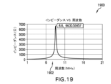
図18は、第1の絶縁性-導電性ストリップ1402が導電体1802および1804により第2の絶縁性-導電性ストリップ1403と電気的に並列に結合されている、誘導性-容量性フィルタアセンブリ1400を例示し、図19は、図18に例示されているように第1の絶縁性-導電性ストリップ1402が第2の絶縁性-導電性ストリップ1403と電気的に並列に結合されている、誘導性-容量性フィルタアセンブリ1400の1つの特定の実施形態のインピーダンス対周波数を示すグラフ1900である。図19から明らかであるように、この特定の実施形態は、8.6MHzの共振周波数1902および共振周波数1902における約6,600オームのピークインピーダンスを有する。
FIG. 18 illustrates an inductive-
図20は、導電体2026により電気的に直列に結合された第1の誘導性-容量性フィルタ2000および第2の誘導性-容量性フィルタ2001の斜視図である。追加の導電体2028および2030は、それぞれ第1および第2の誘導性-容量性フィルタ2000および2001対して電気的インタフェースを提供する。第1の誘導性-容量性フィルタ2000は第1の絶縁性-導電性ストリップ2002を含み、第2の誘導性-容量性フィルタ2001は第2の絶縁性-導電性ストリップ2003を含む。第1の絶縁性-導電性ストリップ2002は、巻回軸2004の周りに導電性ストリップ2010と並行に巻回された絶縁性ストリップ2008を含み、第2の絶縁性-導電性ストリップ2003は、巻回軸2005の周りに導電性ストリップ2011と並行に巻回された絶縁性ストリップ2009を含む。第1の絶縁性-導電性ストリップ2002および第2の絶縁性-導電性ストリップ2003の各々は、例えば、図1~19に関して上述された絶縁性-導電性ストリップの1つ以上に類似する構成を有する。帯域阻止特性は、誘導性-容量性フィルタ2000および/または2001の設計および/または製造中に、例えば図1~19に関して以上で論述したものと類似の方法で、例えば(1)第1の絶縁性-導電性ストリップ2002および/または第2の絶縁性-導電性ストリップ2003の巻きの数を変動させること、(2)誘導性-容量性フィルタ2000および/または2001の内側アパーチャ2020および2021のサイズおよび/または形状を変動させること、(3)絶縁性ストリップ2008および/または絶縁性ストリップ2009の厚みおよび/または誘電特性を変動させること、(4)導電性ストリップ2010および/または導電性ストリップ2011の厚みを変動させること、および/または(5)第1および第2の絶縁性-導電性ストリップ2002および2003の幅2024および/または幅2025をそれぞれ変動させること、によって変動可能である。さらに、第1及び第2の絶縁性-導電性ストリップ2002および2003は、それぞれ3回および4回の巻き2006及び2007を形成するものとして例示されているものの、第1および第2の絶縁性-導電性ストリップ2002および2003の巻きの数は、本明細書の範囲から逸脱することなく変動させられてよい。例示上の明瞭さを促進するために、図20には、巻き2006および2007のいくつかの事例のみがラベル付けされている。さらに、誘導性-容量性フィルタ2000および/または2001は、本明細書の範囲から離れて1つ以上の追加の絶縁性-導電性ストリップを含むように修正され得る。その上、第1の誘導性-容量性フィルタ2000および第2の誘導性-容量性フィルタ2001は、本明細書の範囲から逸脱することなく、電気的に並列に結合され得ると考えられる。
FIG. 20 is a perspective view of first inductive-
図21は、電気的に直列に結合されている、図20の誘導性-容量性フィルタ2000および2001の1つの特定の実施形態のインピーダンス対周波数を示すグラフ2100である。図21から明らかであるように、この特定の実施形態は、約2MHzの第1の共振周波数2102および約26.6MHzの第2の共振周波数2104を有する。第1の共振周波数2102は、第2の誘導性-容量性フィルタ2101と関連した共振周波数であり、第2の共振周波数2104は第1の誘導性-容量性フィルタ2000と関連した共振周波数である。第1の誘導性-容量性フィルタ2000のピークインピーダンスは第2の共振周波数2104において約39,240オームであり、第2の誘導性-容量性フィルタ2001のピークインピーダンスは第1の共振周波数2102において約16,095オームである。
FIG. 21 is a
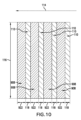
上述の誘導性-容量性フィルタのいずれも、1つ以上の追加の絶縁性-導電性ストリップを含めるように修正可能と考えられる。例えば、図22は、3つの絶縁性-導電性ストリップ2202を含む誘導性-容量性フィルタアセンブリ2200の斜視図であり、図23は、図22のライン23A-23Aに沿って切り取られた誘導性-容量性フィルタアセンブリ2200の断面図である。各々の絶縁性-導電性ストリップ2202は、絶縁性-導電性ストリップ102に類似している。詳細には、第1の絶縁性-導電性ストリップ2202(1)は、第1の絶縁性ストリップ2208(1)と接合された第1の導電性ストリップ2210(1)を含み、第2の絶縁性-導電性ストリップ2202(2)は、第2の絶縁性ストリップ2208(2)と接合された第2の導電性ストリップ2210(2)を含み、第3の絶縁性-導電性ストリップ2202(3)は、第3の絶縁性ストリップ2208(3)と接合された第3の導電性ストリップ2210(3)を含む。いくつかの実施形態において、各々の導電性ストリップ2210は、導電性ストリップの相対する端部に電気的に結合された相対する第1および第2の端子(図示せず)を含む。例示上の明瞭さを促進するため、図23では、絶縁性-導電性ストリップ2202、絶縁性ストリップ2208および導電性ストリップ2210のいくつかの事例のみがラベル付けされている。絶縁性-導電性ストリップ2202の数は、本明細書の範囲から逸脱することなく変動可能であると考えられる。
Any of the inductive-capacitive filters described above could be modified to include one or more additional insulating-conductive strips. For example, FIG. 22 is a perspective view of an inductive-
各々の導電性ストリップ2210は、例えば多重チャネルの帯域阻止フィルタの別個のチャネルとして使用され、ここで各チャネルは類似の帯域阻止特性を有する。帯域阻止特性は、誘導性-容量性フィルタアセンブリ2200の設計および/または製造中に、例えば図1~21に関して以上で論述したものと類似の方法で、例えば(1)絶縁性-導電性ストリップ2202の巻き2206の数を変動させること、(2)誘導性-容量性フィルタアセンブリ2200の内側アパーチャ2220のサイズおよび/または形状を変動させること、(3)絶縁性ストリップ2208の厚みおよび/または誘電特性を変動させること、(4)導電性ストリップ2210の厚みを変動させること、および/または(5)絶縁性-導電性ストリップ2202の幅2224を変動させること、によって変動可能である。例示上の明瞭さを促進するため、図22では、巻き2206の2つの事例のみがラベル付けされている。
Each
誘導性-容量性フィルタアセンブリ2200は、導電性ストリップ2210が電気的に並列に結合される適用において、図3のものと類似の近似電気モデルを有する。対照的に、図24は、導電性ストリップ2210が電気的に並列に結合されていない場合の誘導性-容量性フィルタアセンブリ2000の近似電気モデル2400を例示している。この適用においては、誘導性-容量性フィルタアセンブリ2200は、各々の絶縁性-導電性ストリップ2202がそれぞれの誘導性-容量性フィルタを形成するような形で、それぞれ絶縁性-導電性ストリップ2202(1)、2202(2)および2202(3)に対応する3つのチャネル2402、2404および2406を形成する。コンデンサ2408、インダクタ2410および抵抗器2412は、それぞれチャネル2402のキャパシタンス、インダクタンスおよび抵抗を表わす。コンデンサ2414、インダクタ2416および抵抗器2418は、それぞれチャネル2404のキャパシタンス、インダクタンスおよび抵抗を表わす。コンデンサ2420、インダクタ2422および抵抗器2424は、チャネル2406のキャパシタンス、インダクタンスおよび抵抗を表わす。コンデンサ2426は、チャネル2402とチャネル2404の間の容量結合を表わし、コンデンサ2428は、チャネル2404とチャネル2406の間の容量結合を表わし、コンデンサ2430は、チャネル2402とチャネル2406の間の容量結合を表わす。図24の電気モデル2400は、例示上の単純さのため個別の要素である状態で各構成要素を例示しているが、これらの構成要素の各々は、分散型要素を表わしている。さらに、モデル2400は、コンデンサを通る漏洩電流、インダクタのキャパシタンスまたはコンデンサのインダクタンスなどの高次効果を考慮に入れていない。
Inductive-
絶縁性ストリップおよび導電性ストリップは図1、2、5~15、18、20、22および23の例示において共通の幅を有しているが、絶縁性ストリップの幅および導電性ストリップの幅は同じである必要はない。例えば図25は、図1の誘導性-容量性フィルタと類似の、ただし絶縁性ストリップ108の代りに絶縁性ストリップ2508を含んでいる誘導性-容量性フィルタ2500の図2と類似の断面図である。絶縁性ストリップ2508は、例えば導電性ストリップ110の隣接する区分の偶発的短絡の尤度を減少させるように、導電性ストリップ110の幅よりも大きい幅2516を有する。
Although the insulating strips and conductive strips have a common width in the illustrations of FIGS. does not have to be For example, FIG. 25 is a cross-sectional view similar to FIG. 2 of an inductive-
誘導性-容量性フィルタ100、500、600、700、800、900、1100、1300、1405、1407、2000、2001、2200および2500は、明示的な磁気コアを有しておらず、或いは換言すると、これらの誘導性-容量性フィルタは「空気」コアを有する。しかしながら、本明細書中で開示されている誘導性-容量性フィルタのいずれも、非限定的にフェライト磁性材料または鉄粉磁性材料を含めた磁性材料で形成された明示的な磁気コアを含むように修正可能であると考えられる。部分的磁束経路または完全な磁束経路のいずれかを形成し得る磁気コアは、誘導性-容量性フィルタの共振周波数に影響を及ぼす。詳細には、インダクタンスは、誘導性-容量性フィルタの磁束経路の磁気抵抗の減少と共に増大し、インダクタンスの増大は、フィルタの共振周波数を減少させる。その結果、所与の磁気コアを伴う誘導性-容量性フィルタの共振周波数は、共振周波数が磁性材料の透磁率の増大と共に減少するような形で、磁気コアを形成する磁性材料の透磁率を変動させることによって調整可能である。
The inductive-
図26は、図1の誘導性-容量性フィルタ100と類似の、ただし内側アパーチャ120内に配置されたロッド型の磁気コア2628をさらに含む誘導性-容量性フィルタ2600の斜視図を例示する。ロッド型磁気コア2628は、部分的な磁束経路のみを形成し、或いは換言すると、ロッド型磁気コア2628は共振ストリップ102の周りに閉鎖経路を形成しない。それでも、ロッド型磁気コア2628は、誘導性-容量性フィルタ2600の磁束経路の磁気抵抗を著しく低下させ、そのため、誘導性-容量性フィルタ2600は図1の誘導性-容量性フィルタ100よりも低い共振周波数を有することになる。第1および第2の端子134および136は、例示上の明瞭さを促進するため、図26には示されていない。
FIG. 26 illustrates a perspective view of an inductive-
図27~29は各々、磁気コアが完全な磁束経路を形成している、或いは換言すると、磁気コアが誘導性-容量性フィルタの絶縁性-導電性ストリップの周りに閉鎖経路を形成している、誘導性-容量性フィルタのそれぞれの実施例を例示する。詳細には、図27は、図1の誘導性-容量性フィルタ100と同様の、ただし磁気コア2728をさらに含んでいる誘導性-容量性フィルタ2700の斜視図を例示する。磁気コア2728は、内側アパーチャ120を通って延在する内側支柱(図27には見えず)および内側支柱の相対する端部を連結する外側部分を含んでいた。いくつかの実施形態において、磁気コア2728は、2つの「E字型」コアで形成され、他のいくつかの実施形態において、磁気コア2728は「I字型」コアと「E字型」コアとで形成されている。磁気コア2728は、図26の磁気コア2628よりも低い磁気抵抗の磁束経路を提供し、したがって、図27の誘導性-容量性フィルタ2700は、図26の誘導性-容量性フィルタ2600よりも低い共振周波数を有する。第1および第2の端子134および136は、例示上の明瞭さを促進するため、図27には示されていない。
27-29 each show a magnetic core forming a complete magnetic flux path, or in other words a magnetic core forming a closed path around the insulating-conducting strips of an inductive-capacitive filter. , illustrate respective embodiments of inductive-capacitive filters. Specifically, FIG. 27 illustrates a perspective view of an inductive-
図28は、図1の誘導性-容量性フィルタと同様の、ただし磁気コア2828をさらに含んでいる誘導性-容量性フィルタ2800の斜視図を例示する。いくつかの実施形態において、磁気コア2828は2つの「U字型」コアで形成され、いくつかの実施形態において、磁気コア2828は、「I字型」コアと「U字型」コアとで形成される。磁気コア2828は、図26の磁気コア2628よりも低い磁気抵抗の磁束経路を提供し、したがって、図28の誘導性-容量性フィルタ2800は、図26の誘導性-容量性フィルタ2600よりも低い共振周波数を有する。第1および第2の端子134および136は、例示上の明瞭さを促進するため、図28中には示されていない。
FIG. 28 illustrates a perspective view of an inductive-
図29は、図1の誘導性-容量性フィルタと同様の、ただし磁気コア2928をさらに含んでいる誘導性-容量性フィルタ2900の斜視図を例示する。磁気コア2928は、図27の磁気コア2728と類似しているが、内側アパーチャ120を通って延在する内側支柱(図29には見えず)の相対する端部を連結する丸味のある外側部分を有する。いくつかの実施形態において、磁気コア2928は2つのポット型コア(pot core)で形成されている。磁気コア2928は、図26の磁気コアの磁気コア2628、図27の磁気コア2728または図28の磁気コア2828のいずれよりも低い磁気抵抗の磁束経路を提供し、したがって、図29の誘導性-容量性フィルタ2900は、図26の誘導性-容量性フィルタ2600、図27の誘導性-容量性フィルタ2700または図28の誘導性-容量性フィルタ2800のいずれよりも低い共振周波数を有する。第1および第2の端子134および136は、例示上の明瞭さを促進するため図29には示されていない。
FIG. 29 illustrates a perspective view of an inductive-
本明細書中で開示されている誘導性-容量性フィルタの1つの考えられる適用は、例えば共振周波数から離れた信号は伝送する一方で、フィルタの共振周波数の周りの一定の周波数帯域内の周波数を有する信号を遮断する帯域阻止フィルタを実装する、電気回路におけるものである。例えば、図30は、交流(AC)電力源3002および負荷3004と電気的に直列に結合された誘導性-容量性フィルタ100の事例を含む電気回路3000を例示している。回路3000は、例えば半導体処理システムの一部である。一部の実施形態において、電力源3002は、AC電気格子(electric grid)(例えば50または60ヘルツで動作するもの)、AC発電機、インバータ、オシレータ、音声増幅器または無線周波数増幅器を表わし、負荷3004は、線形負荷(例えば抵抗、誘導および/または容量性負荷)または非線形負荷(例えば、スイッチング電源負荷)を表わす。電気回路3000内で、誘導性-容量性フィルタ100の導電性ストリップ110の第1の端部130は、第1のノード3006において第1の端子134を介して電力源3002に電気的に結合されており、導電性ストリップ110の第2の端部132は、第2のノード3008において端子136を介して負荷3004に電気的に結合されている。こうして、導電性ストリップ110の第1および第2の端部130および132は、電気回路3000の異なるそれぞれのノード3006および3008に対して電気的に結合されている。この特定の適用では、誘導性-容量性フィルタ100は、例えば電力源3002または負荷3004により生成される望ましくない信号の伝送を防止するために、フィルタ100の共振周波数に近い特定の周波数帯域内の信号の伝送を遮断する。誘導性-容量性フィルタ100は、例えば、望ましくない信号の周波数に近いかまたはそれと等しい共振周波数を有するように調整され、こうして、誘導性-容量性フィルタ100は、この周波数で高いインピーダンスを有し、これにより電気回路3000内の望ましくない信号の伝送は実質的に遮断されるようになっている。
One possible application of the inductive-capacitive filter disclosed herein is, for example, to transmit signals away from the resonant frequency, while transmitting frequencies within a certain frequency band around the resonant frequency of the filter. in an electrical circuit that implements a band-stop filter that blocks signals with For example, FIG. 30 illustrates an
AC電力源3002は、本明細書の範囲から逸脱することなく、直流(DC)電力源と置換され得る。例えば、図31は、図30の電気回路3000と同様の、ただしAC電力源3002が直流(DC)電力源3102で置換されている電気回路3100を例示する。DC電力源3102は、例えばDC電力バス、電源、バッテリまたは1つ以上の太陽電池である。
特定の実施形態において、負荷3004は、外部回路(図示せず)に電力供給するため周波数f1でAC出力信号を生成する電源である。この電源は、周波数f1を有するDC電力源2802またはAC電力源3002からのノイズに対する感応性を有し、誘導性-容量性フィルタ100は、周波数f1を有する信号の伝送を遮断するため、適切に調整される。
In a particular embodiment,
電気回路3000および3100は、本明細書の範囲から逸脱することなく、本明細書中で開示された他の誘導性-容量性フィルタのいずれかで誘導性-容量性フィルタ100を置換するように修正され得る。さらに、電気回路3000および2100のトポロジは、本明細書の範囲から逸脱することなく修正可能であ得る。例えば、電気回路3000は、誘導性-容量性フィルタ100の共振周波数に近い周波数を有する信号を除く全ての信号を分路するため、電力源および負荷3104の各々と誘導性-容量性フィルタ100が電気的に並列に結合されるような形で修正可能であり得る。
図32は、誘導性-容量性フィルタアセンブリ2200の一事例、AC電力源3202、第1の負荷3204、第2の負荷3206、および第3の負荷3208を含む電気回路3200を例示する。誘導性-容量性フィルタアセンブリ2200の第1のチャネル2402は、電気回路3200の第1の分岐3210内の第1の負荷3204とAC電力源3202との間で電気的に結合され、誘導性-容量性フィルタアセンブリ2200の第2のチャネル2404は、電気回路3200の第2の分岐3212内の第2の負荷3206とAC電力源3202との間で電気的に結合され、誘導性-容量性フィルタアセンブリ2200の第3のチャネル2406は、電気回路3200の第3の分岐3208内の第3の負荷3208とAC電力源3202との間で電気的に結合される。回路3200は、例えば半導体処理システムの一部である。AC電力源3202は、本明細書の範囲から逸脱することなく、DC電力源と置換されてよい。
FIG. 32 illustrates an example inductive-
特定の実施形態において、第1の負荷3204は、外部回路(図示せず)に電力供給するため第1の周波数f1でAC出力信号を生成する第1の電源であり、第2の負荷3206は、外部回路(図示せず)に電力供給するため第2の周波数f2でAC出力信号を生成する第2の電源であり、第3の負荷3208は、外部回路(図示せず)に電力供給するため第3の周波数f3でAC出力信号を生成する第3の電源である。第1、第2および第3の電源は、周波数f1、周波数f2および周波数f3をそれぞれ有するAC電力源3202からのノイズに対する感応性を有する。したがって、この適用では、誘導性-容量性フィルタ2200の第1のチャネル2402は、周波数f1を有する信号の伝送を遮断するように調整され、誘導性-容量性フィルタ2200の第2のチャネル2404は、周波数f2を有する信号の伝送を遮断するように調整され、誘導性-容量性フィルタ2200の第3のチャネル2406は、周波数f3を有する信号の伝送を遮断するように調整される。
In a particular embodiment, the
図33は、誘導性-容量性フィルタアセンブリ1400の一事例、AC電力源3302、負荷3304を含む電気回路3300を例示する。アセンブリ1400の第1および第2の誘導性-容量性フィルタ1405および1407は、AC電力源3302および負荷3304と電気的に直列に結合されている。回路3300は、例えば半導体処理システムの一部である。AC電力源3302は、本明細書の範囲から逸脱することなくDC電力源と置換されてよい。
FIG. 33 illustrates an
特定の実施形態において、負荷3304は、周波数f1を有するAC電力源3302からのノイズおよび周波数f2を有するAC電力源3302からのノイズに対する感応性を有する。したがって、この適用では、第1の誘導性-容量性フィルタ1405は、周波数f1を有する信号の伝送を遮断するように調整され、第2の誘導性-容量性フィルタ1407は、周波数f2を有する信号の伝送を遮断するように調整される。
In certain embodiments, load 3304 is sensitive to noise from
上述の誘導性-容量性フィルタ、システムおよび関連する方法に対し、本明細書の範囲から離れて変更を加えることができる。したがって、以上の説明内に含まれ添付図面内で示された事柄は、限定的な意味合いにおいてではなく例示的なものとして解釈されるべきであることは留意されるべきである。以下のクレームは、本明細書中に記載の包括的かつ具体的特徴、ならびに言語的にその間に入るものと言われる可能性のある当該フィルタ、方法およびシステムの範囲についての全ての陳述を網羅するように意図されている。
本明細書に開示される発明は以下の態様を含む。
〔態様1〕
誘導性-容量性フィルタにおいて、
巻回軸の周りに巻回された第1の絶縁性-導電性ストリップを含み、
前記第1の絶縁性-導電性ストリップは、第1の絶縁性ストリップと接合された第1の導電性ストリップを含む、誘導性-容量性フィルタ。
〔態様2〕
前記第1の導電性ストリップは、前記巻回軸の周りに前記第1の絶縁性ストリップと並行して巻回されている、態様1に記載の誘導性-容量性フィルタ。
〔態様3〕
前記第1の導電性ストリップは、金属箔で形成され、
前記第1の絶縁性ストリップは、誘電性材料で形成されている、
態様1に記載の誘導性-容量性フィルタ。
〔態様4〕
第1の導電性ストリップは、少なくとも2のアスペクト比を伴う断面部域を有する、態様1に記載の誘導性-容量性フィルタ。
〔態様5〕
前記第1の絶縁性-導電性ストリップは、前記誘導性-容量性フィルタを前記巻回軸の方向に沿って断面で見た場合に分かるように、内側アパーチャを形成する、態様1に記載の誘導性-容量性フィルタ。
〔態様6〕
前記内側アパーチャは、非円形形状を有する、態様5に記載の誘導性-容量性フィルタ。
〔態様7〕
前記内側アパーチャに配置された磁気コアをさらに含む、態様5に記載の誘導性-容量性フィルタ。
〔態様8〕
前記第1の導電性ストリップの相対する第1および第2の端部にそれぞれ電気的に結合された第1および第2の端子をさらに含む、態様1に記載の誘導性-容量性フィルタ。
〔態様9〕
前記巻回軸の周りに巻回された1つ以上の追加の絶縁性-導電性ストリップをさらに含み、各々の追加の絶縁性-導電性ストリップは、それぞれの絶縁性ストリップと共に巻回されたそれぞれの導電性ストリップを含む、態様1に記載の誘導性-容量性フィルタ。
〔態様10〕
巻回軸の周りに同心的に巻回された第1および第2の絶縁性-導電性ストリップを含み、
前記第1の絶縁性-導電性ストリップは、第1の絶縁性ストリップと接合された第1の導電性ストリップを含み、
前記第2の絶縁性-導電性ストリップは、第2の絶縁性ストリップと接合された第2の導電性ストリップを含む、
誘導性-容量性フィルタアセンブリ。
〔態様11〕
前記第1の導電性ストリップは、前記巻回軸の周りに前記第1の絶縁性ストリップと並行して巻回されており、
前記第2の導電性ストリップは、前記巻回軸の周りに前記第2の絶縁性ストリップと並行して巻回されている、
態様10に記載の誘導性-容量性フィルタアセンブリ。
〔態様12〕
前記第1の絶縁性-導電性ストリップは、前記第2の絶縁性-導電性ストリップに対し電気的に結合されている、態様10に記載の誘導性-容量性フィルタアセンブリ。
〔態様13〕
前記第1の絶縁性-導電性ストリップは、前記誘導性-容量性フィルタアセンブリを巻回軸の方向に沿って断面で見た場合に分かるように、前記第2の絶縁性-導電性ストリップの内部に配置されている、態様10に記載の誘導性-容量性フィルタアセンブリ。
〔態様14〕
前記巻回軸の周りに前記第1および第2の絶縁性-導電性ストリップと共に同心的に巻回されている第3の絶縁性-導電性ストリップをさらに含み、
前記第3の絶縁性-導電性ストリップは、第3の絶縁性ストリップと接合された第3の導電性ストリップを含み、
前記第1、第2および第3の絶縁性-導電性ストリップの各々は、それぞれの誘導性-容量性フィルタを形成し、
前記第1の絶縁性-導電性ストリップは、前記誘導性-容量性フィルタアセンブリを前記巻回軸の方向に沿って断面で見た場合に分かるように、前記第2の絶縁性-導電性ストリップの内部に配置されており、
前記第1および第2の絶縁性-導電性ストリップの各々は、前記誘導性-容量性フィルタアセンブリを前記巻回軸の方向に沿って断面で見た場合に分かるように、前記第3の絶縁性-導電性ストリップの内部に配置されている、
態様10に記載の誘導性-容量性フィルタアセンブリ。
〔態様15〕
前記第1および第2の導電性ストリップの各々は、金属箔で形成されており、
前記第1および第2の絶縁性ストリップの各々は、誘電性材料で形成されている、
態様10に記載の誘導性-容量性フィルタアセンブリ。
〔態様16〕
前記第1の導電性ストリップは、少なくとも2のアスペクト比を伴う断面部域を有し、
前記第2の導電性ストリップは、少なくとも2のアスペクト比を伴う断面部域を有する、
態様10に記載の誘導性-容量性フィルタアセンブリ。
〔態様17〕
前記第1および第2の絶縁性-導電性ストリップの各々は、前記巻回軸の周りに多数の巻きを形成する、態様10に記載の誘導性-容量性フィルタアセンブリ。
〔態様18〕
前記第1および第2の絶縁性-導電性ストリップの各々は、巻回軸の周りに異なるそれぞれの数の巻きを形成する、態様10に記載の誘導性-容量性フィルタアセンブリ。
〔態様19〕
前記巻回軸の周りに前記第1および第2の絶縁性-導電性ストリップと共に同心的に巻回されている第3の絶縁性-導電性ストリップをさらに含み、
前記第3の絶縁性-導電性ストリップは、第3の絶縁性ストリップと接合された第3の導電性ストリップを含み、
前記第1、第2および第3の絶縁性-導電性ストリップの各々は、それぞれの誘導性-容量性フィルタを形成する、
態様10に記載の誘導性-容量性フィルタアセンブリ。
〔態様20〕
態様1に記載の前記誘導性-容量性フィルタを含む、電気回路。
〔態様21〕
前記第1の導電性ストリップの相対する第1および第2の端部は、前記電気回路の異なるそれぞれのノードに対して電気的に結合されている、態様20に記載の電気回路。
〔態様22〕
態様1に記載の前記誘導性-容量性フィルタと直列に電気的に結合された交流電源および直流電源のうちの少なくとも1つおよび負荷をさらに含む、態様21に記載の電気回路。
〔態様23〕
態様10に記載の前記誘導性-容量性フィルタアセンブリを含み、
前記第1および第2の絶縁性-導電性ストリップの各々が、電気回路のそれぞれの分岐に対し電気的に結合されている、電気回路。
〔態様24〕
前記第1および第2の絶縁性-導電性ストリップの各々は、電源とそれぞれの電気負荷の間に電気的に結合されている、態様23に記載の電気回路。
Modifications may be made to the inductive-capacitive filters, systems and associated methods described above while departing from the scope hereof. Therefore, it should be noted that the matter contained in the above description and shown in the accompanying drawings should be interpreted in an illustrative rather than a restrictive sense. The following claims cover all statements as to the scope of such filters, methods and systems that may be said to be generic and specific features described herein and linguistically therebetween. is intended to
The invention disclosed in this specification includes the following aspects.
[Aspect 1]
In an inductive-capacitive filter,
including a first insulating-conductive strip wound around a winding axis;
An inductive-capacitive filter, wherein the first insulating-conductive strip comprises a first conductive strip joined with a first insulating strip.
[Aspect 2]
2. The inductive-capacitive filter of
[Aspect 3]
the first conductive strip is formed of a metal foil;
the first insulating strip is formed of a dielectric material;
An inductive-capacitive filter according to
[Aspect 4]
[Aspect 5]
[Aspect 6]
6. The inductive-capacitive filter of aspect 5, wherein the inner aperture has a non-circular shape.
[Aspect 7]
6. The inductive-capacitive filter of aspect 5, further comprising a magnetic core positioned in said inner aperture.
[Aspect 8]
[Aspect 9]
further comprising one or more additional insulating-conductive strips wound around said winding axis, each additional insulating-conductive strip being wound with its respective insulating strip; The inductive-capacitive filter of
[Aspect 10]
comprising first and second insulating-conductive strips concentrically wound about a winding axis;
said first insulating-conductive strip comprising a first conductive strip joined with a first insulating strip;
the second insulating-conductive strip comprises a second conductive strip joined with a second insulating strip;
Inductive-capacitive filter assembly.
[Aspect 11]
the first conductive strip is wound parallel to the first insulating strip about the winding axis;
the second conductive strip is wound parallel to the second insulating strip about the winding axis;
11. An inductive-capacitive filter assembly according to aspect 10.
[Aspect 12]
11. The inductive-capacitive filter assembly of aspect 10, wherein said first insulating-conductive strip is electrically coupled to said second insulating-conductive strip.
[Aspect 13]
The first insulating-conducting strip is the same as the second insulating-conducting strip, as can be seen when the inductive-capacitive filter assembly is viewed in cross-section along the direction of the winding axis. 11. The inductive-capacitive filter assembly of aspect 10, disposed therein.
[Aspect 14]
further comprising a third insulating-conductive strip concentrically wound with said first and second insulating-conductive strips about said winding axis;
said third insulating-conductive strip comprising a third conductive strip joined with a third insulating strip;
each of said first, second and third insulating-conductive strips forming a respective inductive-capacitive filter;
Said first insulating-conducting strip overlaps said second insulating-conducting strip, as can be seen when the inductive-capacitive filter assembly is viewed in cross-section along the direction of said winding axis. is located inside the
Each of the first and second insulative-conductive strips overlaps the third insulative strip, as can be seen when the inductive-capacitive filter assembly is viewed in cross-section along the direction of the winding axis. conductive--located inside the conductive strip,
11. An inductive-capacitive filter assembly according to aspect 10.
[Aspect 15]
each of the first and second conductive strips being formed of a metal foil;
each of the first and second insulating strips being formed of a dielectric material;
11. An inductive-capacitive filter assembly according to aspect 10.
[Aspect 16]
the first conductive strip has a cross-sectional area with an aspect ratio of at least 2;
the second conductive strip has a cross-sectional area with an aspect ratio of at least two;
11. An inductive-capacitive filter assembly according to aspect 10.
[Aspect 17]
11. The inductive-capacitive filter assembly of aspect 10, wherein each of said first and second insulating-conductive strips forms a number of turns about said winding axis.
[Aspect 18]
11. The inductive-capacitive filter assembly of aspect 10, wherein each of said first and second insulating-conductive strips form a different respective number of turns about a winding axis.
[Aspect 19]
further comprising a third insulating-conductive strip concentrically wound with said first and second insulating-conductive strips about said winding axis;
said third insulating-conductive strip comprising a third conductive strip joined with a third insulating strip;
each of said first, second and third insulating-conductive strips forming a respective inductive-capacitive filter;
11. An inductive-capacitive filter assembly according to aspect 10.
[Aspect 20]
An electrical circuit comprising the inductive-capacitive filter of
[Aspect 21]
21. The electrical circuit of aspect 20, wherein opposing first and second ends of said first conductive strip are electrically coupled to different respective nodes of said electrical circuit.
[Aspect 22]
22. The electrical circuit of
[Aspect 23]
comprising the inductive-capacitive filter assembly of aspect 10;
An electrical circuit wherein each of said first and second insulating-conductive strips is electrically coupled to a respective branch of the electrical circuit.
[Aspect 24]
24. The electrical circuit of aspect 23, wherein each of said first and second insulating-conductive strips is electrically coupled between a power source and a respective electrical load.
Claims (19)
複数の絶縁性-導電性ストリップを含み、
該絶縁性-導電性ストリップの各々は、
(a)導電性ストリップと接合された絶縁性ストリップを有し、
(b)複数の絶縁性-導電性ストリップのそれぞれの第1端子端部における共通の電源および導電性ストリップの第2端子端部に接続されたそれぞれの負荷に接続されるときに、整合する目標の共振周波数を中心とする周波数の信号を遮断するように、共通の巻回軸の周りに並行して巻回されている、
誘導性-容量性フィルタアセンブリ。 An inductive-capacitive filter assembly comprising:
including a plurality of insulating-conductive strips;
Each of the insulating-conductive strips comprises:
(a) having an insulating strip joined with a conductive strip;
(b) a plurality of insulating- target matching when connected to a common power source at the respective first terminal ends of the conductive strips and respective loads connected to the second terminal ends of the conductive strips; wound in parallel about a common winding axis so as to block signals at frequencies centered at the resonant frequency of
Inductive-capacitive filter assembly.
前記第1の絶縁性-導電性ストリップおよび前記第2の絶縁性-導電性ストリップの各々の帯域阻止特性は、絶縁性-導電性ストリップの巻数、誘導性-容量性フィルタアセンブリの内側アパーチャのサイズおよび形状、絶縁性ストリップの誘電特性および厚さ、導電性ストリップの厚さ、絶縁性-導電性ストリップの幅、およびこれらの組み合わせのうちの1つ以上に応じて調整される、
請求項1に記載の誘導性-容量性フィルタアセンブリ。 said plurality of insulating-conductive strips comprising a first insulating-conductive strip and a second insulating-conductive strip layered together and wound about said winding axis;
The band rejection characteristics of each of the first insulating-conductive strip and the second insulating-conductive strip are determined by the number of turns of the insulating-conductive strip, the size of the inner aperture of the inductive-capacitive filter assembly and according to one or more of the shape, the dielectric properties and thickness of the insulating strips, the thickness of the conductive strips, the width of the insulating-conductive strips, and combinations thereof;
An inductive-capacitive filter assembly according to claim 1.
前記絶縁性ストリップは、誘電性材料で形成されている、
請求項1に記載の誘導性-容量性フィルタアセンブリ。 The conductive strip is formed of metal foil,
the insulating strip is formed of a dielectric material;
An inductive-capacitive filter assembly according to claim 1.
前記導電性ストリップは、前記巻回軸及び前記半径方向軸の各々に対して平行な平面で見た場合、少なくとも2のアスペクト比を伴う断面形状を有する、請求項1に記載の誘導性-容量性フィルタアセンブリ。 the conductive strip has a radial axis perpendicular to the winding axis and extending away from the winding axis;
2. The inductive-capacitive of claim 1, wherein said conductive strip has a cross-sectional shape with an aspect ratio of at least 2 when viewed in a plane parallel to each of said winding axis and said radial axis. sex filter assembly.
前記第3の絶縁性-導電性ストリップは、第3の絶縁性ストリップと接合された第3の導電性ストリップを含み、
前記第1の絶縁性-導電性ストリップ、第2の絶縁性-導電性ストリップおよび第3の絶縁性-導電性ストリップの各々は、それぞれの誘導性-容量性フィルタを形成する、
請求項2に記載の誘導性-容量性フィルタアセンブリ。 further comprising a third insulating-conductive strip concentrically wound with said first and second insulating-conductive strips about said winding axis;
said third insulating-conductive strip comprising a third conductive strip joined with a third insulating strip;
each of the first insulating-conductive strip, the second insulating-conductive strip and the third insulating-conductive strip forming a respective inductive-capacitive filter;
An inductive-capacitive filter assembly according to claim 2.
少なくとも一つの負荷に接続された電源であって、電源と負荷との間で直列に電気的に接続された誘導性-容量性フィルタを備える電源を具備し、
前記誘導性-容量性フィルタは、
複数の絶縁性-導電性ストリップを有し、
該絶縁性-導電性ストリップの各々は、
(a)導電性ストリップと接合された絶縁性ストリップを有し、
(b)それぞれの負荷に接続されるときに、整合する目標の共振周波数を中心とする周波数を有する電源の信号を遮断するように、共通の巻回軸の周りに並行して巻回されている、
半導体処理装置。 A semiconductor processing apparatus comprising:
a power supply connected to at least one load, the power supply comprising an inductive-capacitive filter electrically connected in series between the power supply and the load;
The inductive-capacitive filter comprises:
having a plurality of insulating-conductive strips;
Each of the insulating-conductive strips comprises:
(a) having an insulating strip joined with a conductive strip;
(b) wound in parallel about a common winding axis so as to block signals of power supplies having frequencies centered on matching target resonant frequencies when connected to their respective loads; there is
Semiconductor processing equipment.
前記3つの負荷の各々は、前記誘導性-容量性フィルタから電力を受領し、
3つの導電性ストリップの各々の第1の端子端部は、前記電源に接続され、
3つの導電性ストリップの各々の第2の端子端部は、3つの負荷の一つに一意的に接続される、
請求項17に記載の半導体処理装置。 the at least one load includes three loads;
each of the three loads receiving power from the inductive-capacitive filter;
a first terminal end of each of the three conductive strips is connected to the power source;
a second terminal end of each of the three conductive strips is uniquely connected to one of the three loads;
18. The semiconductor processing apparatus of claim 17.
Priority Applications (1)
| Application Number | Priority Date | Filing Date | Title |
|---|---|---|---|
| JP2023022186A JP2023059922A (en) | 2017-07-25 | 2023-02-16 | Inductive-capacitive filters and associated systems and methods |
Applications Claiming Priority (3)
| Application Number | Priority Date | Filing Date | Title |
|---|---|---|---|
| US201762536806P | 2017-07-25 | 2017-07-25 | |
| US62/536,806 | 2017-07-25 | ||
| PCT/US2018/043651 WO2019023325A1 (en) | 2017-07-25 | 2018-07-25 | Inductive-capacitive filters and associated systems and methods |
Related Child Applications (1)
| Application Number | Title | Priority Date | Filing Date |
|---|---|---|---|
| JP2023022186A Division JP2023059922A (en) | 2017-07-25 | 2023-02-16 | Inductive-capacitive filters and associated systems and methods |
Publications (3)
| Publication Number | Publication Date |
|---|---|
| JP2020529177A JP2020529177A (en) | 2020-10-01 |
| JP2020529177A5 JP2020529177A5 (en) | 2021-12-23 |
| JP7231629B2 true JP7231629B2 (en) | 2023-03-01 |
Family
ID=65040341
Family Applications (2)
| Application Number | Title | Priority Date | Filing Date |
|---|---|---|---|
| JP2020527840A Active JP7231629B2 (en) | 2017-07-25 | 2018-07-25 | Inductive-capacitive filters and related systems and methods |
| JP2023022186A Pending JP2023059922A (en) | 2017-07-25 | 2023-02-16 | Inductive-capacitive filters and associated systems and methods |
Family Applications After (1)
| Application Number | Title | Priority Date | Filing Date |
|---|---|---|---|
| JP2023022186A Pending JP2023059922A (en) | 2017-07-25 | 2023-02-16 | Inductive-capacitive filters and associated systems and methods |
Country Status (5)
| Country | Link |
|---|---|
| US (2) | US11183985B2 (en) |
| EP (2) | EP3659255B1 (en) |
| JP (2) | JP7231629B2 (en) |
| CN (2) | CN116886065A (en) |
| WO (1) | WO2019023325A1 (en) |
Families Citing this family (1)
| Publication number | Priority date | Publication date | Assignee | Title |
|---|---|---|---|---|
| US11831290B2 (en) * | 2017-07-25 | 2023-11-28 | Wjlp Company Inc. | Inductive-capacitive filters and associated systems and methods |
Family Cites Families (19)
| Publication number | Priority date | Publication date | Assignee | Title |
|---|---|---|---|---|
| US2027067A (en) * | 1930-11-05 | 1936-01-07 | Siemens Ag | Filter circuit |
| US2884605A (en) * | 1953-09-11 | 1959-04-28 | Cornell Dubilier Electric | Electrical suppressor |
| US3911332A (en) * | 1971-12-29 | 1975-10-07 | George M Kunkel | Wound transformers and machine for making the same |
| US4048593A (en) * | 1974-05-13 | 1977-09-13 | Zillman Jack H | Electrical component for providing integrated inductive-capacitive networks |
| JPS5483736A (en) * | 1977-12-16 | 1979-07-04 | Matsushita Electric Ind Co Ltd | Noise filter |
| JP2770278B2 (en) | 1987-01-14 | 1998-06-25 | 毅 池田 | Noise filter and method of manufacturing the same |
| DE3909528A1 (en) | 1988-03-23 | 1989-10-12 | Murata Manufacturing Co | IMPACT FILTER |
| JP2728439B2 (en) * | 1988-07-14 | 1998-03-18 | 毅 池田 | Four-terminal noise filter and method of manufacturing the same |
| US5153812A (en) * | 1989-06-16 | 1992-10-06 | Mitsubishi Denki Kabushiki Kaisha | Composite LC element |
| JPH04199502A (en) | 1990-11-29 | 1992-07-20 | Mitsubishi Electric Corp | Lc composite element |
| JP3184580B2 (en) * | 1991-10-29 | 2001-07-09 | 新潟精密株式会社 | Resonance filter |
| JPH05251267A (en) * | 1992-03-06 | 1993-09-28 | Okaya Electric Ind Co Ltd | Composite electronic component |
| US5337028A (en) * | 1992-05-27 | 1994-08-09 | Sundstrand Corporation | Multilayered distributed filter |
| JPH0745476A (en) * | 1993-07-26 | 1995-02-14 | Alps Electric Co Ltd | Lc filter and fabrication thereof |
| JPH07122460A (en) * | 1993-10-21 | 1995-05-12 | Niigata Seimitsu Kk | Lc noise filter and its manufacture |
| JPH08162367A (en) * | 1994-12-08 | 1996-06-21 | Nissei Denki Kk | Noise filter |
| US6208225B1 (en) * | 1999-02-25 | 2001-03-27 | Formfactor, Inc. | Filter structures for integrated circuit interfaces |
| US6476689B1 (en) * | 1999-09-21 | 2002-11-05 | Murata Manufacturing Co., Ltd. | LC filter with capacitor electrode plate not interfering with flux of two coils |
| EP3269419A1 (en) * | 2013-08-04 | 2018-01-17 | Greatbatch Ltd. | Multilayer planar spiral inductor filter for medical, therapeutic or diagnostic applications |
-
2018
- 2018-07-25 WO PCT/US2018/043651 patent/WO2019023325A1/en unknown
- 2018-07-25 CN CN202311050720.4A patent/CN116886065A/en active Pending
- 2018-07-25 JP JP2020527840A patent/JP7231629B2/en active Active
- 2018-07-25 US US16/633,409 patent/US11183985B2/en active Active
- 2018-07-25 EP EP18837308.8A patent/EP3659255B1/en active Active
- 2018-07-25 CN CN201880048147.4A patent/CN110945784B/en active Active
- 2018-07-25 EP EP23163386.8A patent/EP4220956A3/en active Pending
-
2023
- 2023-02-16 JP JP2023022186A patent/JP2023059922A/en active Pending
- 2023-11-27 US US18/519,421 patent/US20240106405A1/en active Pending
Also Published As
| Publication number | Publication date |
|---|---|
| EP3659255A1 (en) | 2020-06-03 |
| EP4220956A2 (en) | 2023-08-02 |
| WO2019023325A1 (en) | 2019-01-31 |
| CN110945784B (en) | 2023-08-22 |
| US11183985B2 (en) | 2021-11-23 |
| US20200366262A1 (en) | 2020-11-19 |
| EP3659255A4 (en) | 2021-10-27 |
| JP2020529177A (en) | 2020-10-01 |
| JP2023059922A (en) | 2023-04-27 |
| EP3659255B1 (en) | 2023-05-03 |
| CN110945784A (en) | 2020-03-31 |
| US20240106405A1 (en) | 2024-03-28 |
| CN116886065A (en) | 2023-10-13 |
| EP4220956A3 (en) | 2023-08-09 |
Similar Documents
| Publication | Publication Date | Title |
|---|---|---|
| JP6937741B2 (en) | Single layer multimode antenna for wireless power transfer using magnetic field coupling | |
| US6476689B1 (en) | LC filter with capacitor electrode plate not interfering with flux of two coils | |
| JP3311391B2 (en) | Leakage inductance reducing transformer, high frequency circuit and power converter using the same, and method of reducing leakage inductance in transformer | |
| US20240106405A1 (en) | Inductive-capacitive filters and associated systems and methods | |
| RU2735240C2 (en) | Device intended for substantially resonating, suitable for radio-frequency power transmission, as well as a system including such a device and used to generate plasma | |
| GB2447963A (en) | Transformer with a plurality of primary and secondary magnetic circuits linked by an electrically conductive loop | |
| EP0468509A2 (en) | Matching network | |
| JP2014160704A (en) | Coil structure and electronic apparatus | |
| WO2005048451A1 (en) | Communication transformer | |
| JP5252564B2 (en) | Inductance element | |
| US11831290B2 (en) | Inductive-capacitive filters and associated systems and methods | |
| JP2001503201A (en) | Inductor | |
| JP2020529177A5 (en) | ||
| US9019044B2 (en) | Filter for a magnetron power supply lead | |
| JP6699354B2 (en) | Coil parts | |
| Reatti et al. | Solid and Litz-wire winding non-linear resistance comparison | |
| JPH01162312A (en) | Composite inductance element | |
| US11908603B2 (en) | Inductor and voltage converter using it | |
| RU118084U1 (en) | HIGH FREQUENCY BROADBAND RELATED AUTO TRANSFORMER | |
| JP2005123751A (en) | Electric noise filter and electric noise eliminating method | |
| RU118469U1 (en) | TOROIDAL TRANSFORMER | |
| JP2010074020A (en) | Inductance element | |
| WO2021146574A1 (en) | Hybrid core magnetics | |
| JPS59212013A (en) | Noise filter | |
| JPH0922857A (en) | Electronic parts |
Legal Events
| Date | Code | Title | Description |
|---|---|---|---|
| A521 | Request for written amendment filed |
Free format text: JAPANESE INTERMEDIATE CODE: A523 Effective date: 20210721 |
|
| A621 | Written request for application examination |
Free format text: JAPANESE INTERMEDIATE CODE: A621 Effective date: 20210721 |
|
| A521 | Request for written amendment filed |
Free format text: JAPANESE INTERMEDIATE CODE: A523 Effective date: 20210802 |
|
| A521 | Request for written amendment filed |
Free format text: JAPANESE INTERMEDIATE CODE: A523 Effective date: 20211111 |
|
| A871 | Explanation of circumstances concerning accelerated examination |
Free format text: JAPANESE INTERMEDIATE CODE: A871 Effective date: 20211111 |
|
| A131 | Notification of reasons for refusal |
Free format text: JAPANESE INTERMEDIATE CODE: A131 Effective date: 20220118 |
|
| A601 | Written request for extension of time |
Free format text: JAPANESE INTERMEDIATE CODE: A601 Effective date: 20220418 |
|
| A521 | Request for written amendment filed |
Free format text: JAPANESE INTERMEDIATE CODE: A523 Effective date: 20220713 |
|
| A131 | Notification of reasons for refusal |
Free format text: JAPANESE INTERMEDIATE CODE: A131 Effective date: 20220809 |
|
| A521 | Request for written amendment filed |
Free format text: JAPANESE INTERMEDIATE CODE: A523 Effective date: 20221109 |
|
| TRDD | Decision of grant or rejection written | ||
| A01 | Written decision to grant a patent or to grant a registration (utility model) |
Free format text: JAPANESE INTERMEDIATE CODE: A01 Effective date: 20230117 |
|
| A61 | First payment of annual fees (during grant procedure) |
Free format text: JAPANESE INTERMEDIATE CODE: A61 Effective date: 20230216 |
|
| R150 | Certificate of patent or registration of utility model |
Ref document number: 7231629 Country of ref document: JP Free format text: JAPANESE INTERMEDIATE CODE: R150 |