JP7231120B2 - Epitaxial wafer manufacturing method - Google Patents
Epitaxial wafer manufacturing method Download PDFInfo
- Publication number
- JP7231120B2 JP7231120B2 JP2022552294A JP2022552294A JP7231120B2 JP 7231120 B2 JP7231120 B2 JP 7231120B2 JP 2022552294 A JP2022552294 A JP 2022552294A JP 2022552294 A JP2022552294 A JP 2022552294A JP 7231120 B2 JP7231120 B2 JP 7231120B2
- Authority
- JP
- Japan
- Prior art keywords
- single crystal
- oxygen
- crystal silicon
- layer
- atomic layer
- Prior art date
- Legal status (The legal status is an assumption and is not a legal conclusion. Google has not performed a legal analysis and makes no representation as to the accuracy of the status listed.)
- Active
Links
- 238000004519 manufacturing process Methods 0.000 title claims description 28
- QVGXLLKOCUKJST-UHFFFAOYSA-N atomic oxygen Chemical compound [O] QVGXLLKOCUKJST-UHFFFAOYSA-N 0.000 claims description 115
- 239000001301 oxygen Substances 0.000 claims description 115
- 229910052760 oxygen Inorganic materials 0.000 claims description 115
- 229910021421 monocrystalline silicon Inorganic materials 0.000 claims description 72
- KRHYYFGTRYWZRS-UHFFFAOYSA-N Fluorane Chemical compound F KRHYYFGTRYWZRS-UHFFFAOYSA-N 0.000 claims description 32
- XLYOFNOQVPJJNP-UHFFFAOYSA-N water Substances O XLYOFNOQVPJJNP-UHFFFAOYSA-N 0.000 claims description 17
- 238000000927 vapour-phase epitaxy Methods 0.000 claims 1
- 239000010410 layer Substances 0.000 description 114
- 235000012431 wafers Nutrition 0.000 description 78
- 238000000034 method Methods 0.000 description 42
- XUIMIQQOPSSXEZ-UHFFFAOYSA-N Silicon Chemical compound [Si] XUIMIQQOPSSXEZ-UHFFFAOYSA-N 0.000 description 21
- 229910052710 silicon Inorganic materials 0.000 description 21
- 239000000758 substrate Substances 0.000 description 21
- 238000005247 gettering Methods 0.000 description 19
- 239000010703 silicon Substances 0.000 description 19
- 125000004429 atom Chemical group 0.000 description 17
- 239000001257 hydrogen Substances 0.000 description 10
- 229910052739 hydrogen Inorganic materials 0.000 description 10
- 239000007789 gas Substances 0.000 description 9
- UFHFLCQGNIYNRP-UHFFFAOYSA-N Hydrogen Chemical compound [H][H] UFHFLCQGNIYNRP-UHFFFAOYSA-N 0.000 description 8
- 230000000052 comparative effect Effects 0.000 description 7
- 229910052751 metal Inorganic materials 0.000 description 7
- 230000001590 oxidative effect Effects 0.000 description 7
- 238000001004 secondary ion mass spectrometry Methods 0.000 description 7
- 238000004627 transmission electron microscopy Methods 0.000 description 7
- 229910021417 amorphous silicon Inorganic materials 0.000 description 6
- 230000015572 biosynthetic process Effects 0.000 description 6
- 238000010438 heat treatment Methods 0.000 description 6
- 239000002184 metal Substances 0.000 description 6
- 238000000231 atomic layer deposition Methods 0.000 description 5
- 230000000694 effects Effects 0.000 description 5
- 230000003647 oxidation Effects 0.000 description 5
- 238000007254 oxidation reaction Methods 0.000 description 5
- 238000004140 cleaning Methods 0.000 description 4
- 239000013078 crystal Substances 0.000 description 4
- 230000007547 defect Effects 0.000 description 4
- 238000000151 deposition Methods 0.000 description 4
- 229910021420 polycrystalline silicon Inorganic materials 0.000 description 4
- 238000005406 washing Methods 0.000 description 4
- 238000002425 crystallisation Methods 0.000 description 3
- 230000008025 crystallization Effects 0.000 description 3
- 239000012535 impurity Substances 0.000 description 3
- 125000004430 oxygen atom Chemical group O* 0.000 description 3
- 239000000126 substance Substances 0.000 description 3
- IJGRMHOSHXDMSA-UHFFFAOYSA-N Atomic nitrogen Chemical compound N#N IJGRMHOSHXDMSA-UHFFFAOYSA-N 0.000 description 2
- CBENFWSGALASAD-UHFFFAOYSA-N Ozone Chemical compound [O-][O+]=O CBENFWSGALASAD-UHFFFAOYSA-N 0.000 description 2
- BLRPTPMANUNPDV-UHFFFAOYSA-N Silane Chemical compound [SiH4] BLRPTPMANUNPDV-UHFFFAOYSA-N 0.000 description 2
- 238000010306 acid treatment Methods 0.000 description 2
- 230000005540 biological transmission Effects 0.000 description 2
- 239000012159 carrier gas Substances 0.000 description 2
- 230000003749 cleanliness Effects 0.000 description 2
- 238000009833 condensation Methods 0.000 description 2
- 230000005494 condensation Effects 0.000 description 2
- 238000007796 conventional method Methods 0.000 description 2
- 230000008021 deposition Effects 0.000 description 2
- 238000010586 diagram Methods 0.000 description 2
- 150000002431 hydrogen Chemical class 0.000 description 2
- 238000005259 measurement Methods 0.000 description 2
- 238000001000 micrograph Methods 0.000 description 2
- 239000004065 semiconductor Substances 0.000 description 2
- 239000002356 single layer Substances 0.000 description 2
- ZOXJGFHDIHLPTG-UHFFFAOYSA-N Boron Chemical compound [B] ZOXJGFHDIHLPTG-UHFFFAOYSA-N 0.000 description 1
- MYMOFIZGZYHOMD-UHFFFAOYSA-N Dioxygen Chemical compound O=O MYMOFIZGZYHOMD-UHFFFAOYSA-N 0.000 description 1
- 238000005422 blasting Methods 0.000 description 1
- 238000009835 boiling Methods 0.000 description 1
- 229910052796 boron Inorganic materials 0.000 description 1
- 229910052799 carbon Inorganic materials 0.000 description 1
- -1 carbon ions Chemical class 0.000 description 1
- 238000009792 diffusion process Methods 0.000 description 1
- 229910001882 dioxygen Inorganic materials 0.000 description 1
- 230000008034 disappearance Effects 0.000 description 1
- PZPGRFITIJYNEJ-UHFFFAOYSA-N disilane Chemical compound [SiH3][SiH3] PZPGRFITIJYNEJ-UHFFFAOYSA-N 0.000 description 1
- 238000001035 drying Methods 0.000 description 1
- 238000005516 engineering process Methods 0.000 description 1
- 230000001747 exhibiting effect Effects 0.000 description 1
- 238000004880 explosion Methods 0.000 description 1
- 229910001385 heavy metal Inorganic materials 0.000 description 1
- CUPFNGOKRMWUOO-UHFFFAOYSA-N hydron;difluoride Chemical compound F.F CUPFNGOKRMWUOO-UHFFFAOYSA-N 0.000 description 1
- 238000003384 imaging method Methods 0.000 description 1
- 239000011261 inert gas Substances 0.000 description 1
- 238000004518 low pressure chemical vapour deposition Methods 0.000 description 1
- 229910052757 nitrogen Inorganic materials 0.000 description 1
- 239000005416 organic matter Substances 0.000 description 1
- 239000002245 particle Substances 0.000 description 1
- 229920005591 polysilicon Polymers 0.000 description 1
- 238000001556 precipitation Methods 0.000 description 1
- 238000004544 sputter deposition Methods 0.000 description 1
Images


Classifications
-
- C—CHEMISTRY; METALLURGY
- C30—CRYSTAL GROWTH
- C30B—SINGLE-CRYSTAL GROWTH; UNIDIRECTIONAL SOLIDIFICATION OF EUTECTIC MATERIAL OR UNIDIRECTIONAL DEMIXING OF EUTECTOID MATERIAL; REFINING BY ZONE-MELTING OF MATERIAL; PRODUCTION OF A HOMOGENEOUS POLYCRYSTALLINE MATERIAL WITH DEFINED STRUCTURE; SINGLE CRYSTALS OR HOMOGENEOUS POLYCRYSTALLINE MATERIAL WITH DEFINED STRUCTURE; AFTER-TREATMENT OF SINGLE CRYSTALS OR A HOMOGENEOUS POLYCRYSTALLINE MATERIAL WITH DEFINED STRUCTURE; APPARATUS THEREFOR
- C30B25/00—Single-crystal growth by chemical reaction of reactive gases, e.g. chemical vapour-deposition growth
- C30B25/02—Epitaxial-layer growth
- C30B25/18—Epitaxial-layer growth characterised by the substrate
- C30B25/186—Epitaxial-layer growth characterised by the substrate being specially pre-treated by, e.g. chemical or physical means
-
- H—ELECTRICITY
- H01—ELECTRIC ELEMENTS
- H01L—SEMICONDUCTOR DEVICES NOT COVERED BY CLASS H10
- H01L21/00—Processes or apparatus adapted for the manufacture or treatment of semiconductor or solid state devices or of parts thereof
- H01L21/02—Manufacture or treatment of semiconductor devices or of parts thereof
- H01L21/04—Manufacture or treatment of semiconductor devices or of parts thereof the devices having at least one potential-jump barrier or surface barrier, e.g. PN junction, depletion layer or carrier concentration layer
- H01L21/18—Manufacture or treatment of semiconductor devices or of parts thereof the devices having at least one potential-jump barrier or surface barrier, e.g. PN junction, depletion layer or carrier concentration layer the devices having semiconductor bodies comprising elements of Group IV of the Periodic System or AIIIBV compounds with or without impurities, e.g. doping materials
- H01L21/30—Treatment of semiconductor bodies using processes or apparatus not provided for in groups H01L21/20 - H01L21/26
- H01L21/322—Treatment of semiconductor bodies using processes or apparatus not provided for in groups H01L21/20 - H01L21/26 to modify their internal properties, e.g. to produce internal imperfections
- H01L21/3221—Treatment of semiconductor bodies using processes or apparatus not provided for in groups H01L21/20 - H01L21/26 to modify their internal properties, e.g. to produce internal imperfections of silicon bodies, e.g. for gettering
-
- C—CHEMISTRY; METALLURGY
- C30—CRYSTAL GROWTH
- C30B—SINGLE-CRYSTAL GROWTH; UNIDIRECTIONAL SOLIDIFICATION OF EUTECTIC MATERIAL OR UNIDIRECTIONAL DEMIXING OF EUTECTOID MATERIAL; REFINING BY ZONE-MELTING OF MATERIAL; PRODUCTION OF A HOMOGENEOUS POLYCRYSTALLINE MATERIAL WITH DEFINED STRUCTURE; SINGLE CRYSTALS OR HOMOGENEOUS POLYCRYSTALLINE MATERIAL WITH DEFINED STRUCTURE; AFTER-TREATMENT OF SINGLE CRYSTALS OR A HOMOGENEOUS POLYCRYSTALLINE MATERIAL WITH DEFINED STRUCTURE; APPARATUS THEREFOR
- C30B25/00—Single-crystal growth by chemical reaction of reactive gases, e.g. chemical vapour-deposition growth
- C30B25/02—Epitaxial-layer growth
- C30B25/18—Epitaxial-layer growth characterised by the substrate
- C30B25/20—Epitaxial-layer growth characterised by the substrate the substrate being of the same materials as the epitaxial layer
-
- C—CHEMISTRY; METALLURGY
- C30—CRYSTAL GROWTH
- C30B—SINGLE-CRYSTAL GROWTH; UNIDIRECTIONAL SOLIDIFICATION OF EUTECTIC MATERIAL OR UNIDIRECTIONAL DEMIXING OF EUTECTOID MATERIAL; REFINING BY ZONE-MELTING OF MATERIAL; PRODUCTION OF A HOMOGENEOUS POLYCRYSTALLINE MATERIAL WITH DEFINED STRUCTURE; SINGLE CRYSTALS OR HOMOGENEOUS POLYCRYSTALLINE MATERIAL WITH DEFINED STRUCTURE; AFTER-TREATMENT OF SINGLE CRYSTALS OR A HOMOGENEOUS POLYCRYSTALLINE MATERIAL WITH DEFINED STRUCTURE; APPARATUS THEREFOR
- C30B25/00—Single-crystal growth by chemical reaction of reactive gases, e.g. chemical vapour-deposition growth
- C30B25/02—Epitaxial-layer growth
- C30B25/22—Sandwich processes
-
- C—CHEMISTRY; METALLURGY
- C30—CRYSTAL GROWTH
- C30B—SINGLE-CRYSTAL GROWTH; UNIDIRECTIONAL SOLIDIFICATION OF EUTECTIC MATERIAL OR UNIDIRECTIONAL DEMIXING OF EUTECTOID MATERIAL; REFINING BY ZONE-MELTING OF MATERIAL; PRODUCTION OF A HOMOGENEOUS POLYCRYSTALLINE MATERIAL WITH DEFINED STRUCTURE; SINGLE CRYSTALS OR HOMOGENEOUS POLYCRYSTALLINE MATERIAL WITH DEFINED STRUCTURE; AFTER-TREATMENT OF SINGLE CRYSTALS OR A HOMOGENEOUS POLYCRYSTALLINE MATERIAL WITH DEFINED STRUCTURE; APPARATUS THEREFOR
- C30B29/00—Single crystals or homogeneous polycrystalline material with defined structure characterised by the material or by their shape
- C30B29/02—Elements
- C30B29/06—Silicon
-
- H—ELECTRICITY
- H01—ELECTRIC ELEMENTS
- H01L—SEMICONDUCTOR DEVICES NOT COVERED BY CLASS H10
- H01L21/00—Processes or apparatus adapted for the manufacture or treatment of semiconductor or solid state devices or of parts thereof
- H01L21/02—Manufacture or treatment of semiconductor devices or of parts thereof
- H01L21/02104—Forming layers
- H01L21/02365—Forming inorganic semiconducting materials on a substrate
- H01L21/02367—Substrates
- H01L21/0237—Materials
- H01L21/02373—Group 14 semiconducting materials
- H01L21/02381—Silicon, silicon germanium, germanium
-
- H—ELECTRICITY
- H01—ELECTRIC ELEMENTS
- H01L—SEMICONDUCTOR DEVICES NOT COVERED BY CLASS H10
- H01L21/00—Processes or apparatus adapted for the manufacture or treatment of semiconductor or solid state devices or of parts thereof
- H01L21/02—Manufacture or treatment of semiconductor devices or of parts thereof
- H01L21/02104—Forming layers
- H01L21/02365—Forming inorganic semiconducting materials on a substrate
- H01L21/02436—Intermediate layers between substrates and deposited layers
- H01L21/02439—Materials
- H01L21/02441—Group 14 semiconducting materials
- H01L21/0245—Silicon, silicon germanium, germanium
-
- H—ELECTRICITY
- H01—ELECTRIC ELEMENTS
- H01L—SEMICONDUCTOR DEVICES NOT COVERED BY CLASS H10
- H01L21/00—Processes or apparatus adapted for the manufacture or treatment of semiconductor or solid state devices or of parts thereof
- H01L21/02—Manufacture or treatment of semiconductor devices or of parts thereof
- H01L21/02104—Forming layers
- H01L21/02365—Forming inorganic semiconducting materials on a substrate
- H01L21/02436—Intermediate layers between substrates and deposited layers
- H01L21/02439—Materials
- H01L21/02488—Insulating materials
-
- H—ELECTRICITY
- H01—ELECTRIC ELEMENTS
- H01L—SEMICONDUCTOR DEVICES NOT COVERED BY CLASS H10
- H01L21/00—Processes or apparatus adapted for the manufacture or treatment of semiconductor or solid state devices or of parts thereof
- H01L21/02—Manufacture or treatment of semiconductor devices or of parts thereof
- H01L21/02104—Forming layers
- H01L21/02365—Forming inorganic semiconducting materials on a substrate
- H01L21/02436—Intermediate layers between substrates and deposited layers
- H01L21/02494—Structure
- H01L21/02496—Layer structure
- H01L21/02505—Layer structure consisting of more than two layers
- H01L21/02507—Alternating layers, e.g. superlattice
-
- H—ELECTRICITY
- H01—ELECTRIC ELEMENTS
- H01L—SEMICONDUCTOR DEVICES NOT COVERED BY CLASS H10
- H01L21/00—Processes or apparatus adapted for the manufacture or treatment of semiconductor or solid state devices or of parts thereof
- H01L21/02—Manufacture or treatment of semiconductor devices or of parts thereof
- H01L21/02104—Forming layers
- H01L21/02365—Forming inorganic semiconducting materials on a substrate
- H01L21/02518—Deposited layers
- H01L21/02521—Materials
- H01L21/02524—Group 14 semiconducting materials
- H01L21/02532—Silicon, silicon germanium, germanium
-
- H—ELECTRICITY
- H01—ELECTRIC ELEMENTS
- H01L—SEMICONDUCTOR DEVICES NOT COVERED BY CLASS H10
- H01L21/00—Processes or apparatus adapted for the manufacture or treatment of semiconductor or solid state devices or of parts thereof
- H01L21/02—Manufacture or treatment of semiconductor devices or of parts thereof
- H01L21/02104—Forming layers
- H01L21/02365—Forming inorganic semiconducting materials on a substrate
- H01L21/02656—Special treatments
- H01L21/02658—Pretreatments
- H01L21/02661—In-situ cleaning
-
- H—ELECTRICITY
- H01—ELECTRIC ELEMENTS
- H01L—SEMICONDUCTOR DEVICES NOT COVERED BY CLASS H10
- H01L21/00—Processes or apparatus adapted for the manufacture or treatment of semiconductor or solid state devices or of parts thereof
- H01L21/02—Manufacture or treatment of semiconductor devices or of parts thereof
- H01L21/02104—Forming layers
- H01L21/02365—Forming inorganic semiconducting materials on a substrate
- H01L21/02518—Deposited layers
- H01L21/02587—Structure
- H01L21/0259—Microstructure
- H01L21/02595—Microstructure polycrystalline
-
- H—ELECTRICITY
- H01—ELECTRIC ELEMENTS
- H01L—SEMICONDUCTOR DEVICES NOT COVERED BY CLASS H10
- H01L21/00—Processes or apparatus adapted for the manufacture or treatment of semiconductor or solid state devices or of parts thereof
- H01L21/02—Manufacture or treatment of semiconductor devices or of parts thereof
- H01L21/02104—Forming layers
- H01L21/02365—Forming inorganic semiconducting materials on a substrate
- H01L21/02612—Formation types
- H01L21/02617—Deposition types
Landscapes
- Engineering & Computer Science (AREA)
- Chemical & Material Sciences (AREA)
- Condensed Matter Physics & Semiconductors (AREA)
- Physics & Mathematics (AREA)
- General Physics & Mathematics (AREA)
- Manufacturing & Machinery (AREA)
- Computer Hardware Design (AREA)
- Microelectronics & Electronic Packaging (AREA)
- Power Engineering (AREA)
- Materials Engineering (AREA)
- Crystallography & Structural Chemistry (AREA)
- Metallurgy (AREA)
- Organic Chemistry (AREA)
- General Chemical & Material Sciences (AREA)
- Chemical Kinetics & Catalysis (AREA)
Description
本発明は、エピタキシャルウェーハの製造方法に関する。 The present invention relates to an epitaxial wafer manufacturing method.
固体撮像素子やその他のトランジスタをはじめとした半導体素子を形成するシリコン基板には、重金属をはじめとした素子特性を狂わせる元素をゲッタリングする機能を持つことが求められる。ゲッタリングには、シリコン基板裏面に多結晶シリコン(Poly-Si)層を持たせたり、ブラスト加工によりダメージを持たせた層を形成する方法や、高濃度ボロンのシリコン基板を利用したり、析出物を形成させたりとさまざまな手法が提案、実用化されている。酸素析出によるゲッタリングは、電気陰性度が大きい酸素に対して、イオン化傾向が大きい(電気陰性度が小さい)金属を取り込むことでゲッタリングする。 Silicon substrates on which semiconductor devices such as solid-state imaging devices and other transistors are formed are required to have the function of gettering elements that disturb device characteristics, such as heavy metals. For gettering, a polycrystalline silicon (Poly-Si) layer is provided on the back surface of the silicon substrate, a method is used to form a layer damaged by blasting, a silicon substrate with a high concentration of boron is used, or a deposition method is used. Various methods have been proposed and put into practical use, such as forming objects. In the gettering by oxygen precipitation, a metal with a high ionization tendency (low electronegativity) is gettered by oxygen with a high electronegativity.
また、素子の活性領域近傍にゲッタリング層を形成する、いわゆる近接ゲッタリングも提案されている。例えば、炭素をイオン注入した基板の上にシリコンをエピタキシャル成長させた基板などがある。ゲッタリングでは、ゲッタリングサイト(金属が単元素で存在するよりも、サイトで結合やクラスタリングすることで系全体のエネルギーが低下する)まで元素が拡散する必要がある。シリコン中に含まれる金属元素の拡散係数は元素により異なり、また近年のプロセス低温化によりゲッタリングサイトまで金属が拡散することが出来なくなることを考慮して、近接ゲッタリングの手法が提案されている。 Also, so-called proximity gettering, in which a gettering layer is formed in the vicinity of the active region of the device, has been proposed. For example, there is a substrate in which silicon is epitaxially grown on a substrate into which carbon ions are implanted. In gettering, the element must diffuse to the gettering site (the energy of the entire system is lowered by bonding or clustering at the site rather than when the metal exists as a single element). Considering that the diffusion coefficient of metal elements contained in silicon differs depending on the element, and that the metal cannot diffuse to the gettering site due to the recent decrease in process temperature, a method of proximity gettering has been proposed. .
近接ゲッタリングに酸素を用いることが出来れば、非常に有力なゲッタリング層をもったシリコン基板となると考えられる。特に、エピタキシャル層の途中に酸素原子層を有するエピタキシャルウェーハであれば、近年の低温プロセスにおいても確実に金属不純物をゲッタリングすることができる。 If oxygen can be used for proximity gettering, a silicon substrate with a very powerful gettering layer can be expected. In particular, if the epitaxial wafer has an oxygen atomic layer in the middle of the epitaxial layer, metal impurities can be gettered reliably even in recent low-temperature processes.
以上、金属不純物をゲッタリングすることを中心に述べてきたが、例えば、酸素の効果としては、CVD酸化膜を裏面に形成することでエピタキシャル成長時のオートドープを防ぐ効果が知られている。 The gettering of metal impurities has been described above. For example, as an effect of oxygen, it is known that forming a CVD oxide film on the back surface prevents autodoping during epitaxial growth.
先行技術について言及する。特許文献1には、構造としてはシリコンの上に酸素の薄い層を形成しさらにシリコンを成長させる方法が記載されている。この方法は、ALD(「Atomic layer deposition」、「原子層堆積法」)をベースとした技術である。ALDは対象原子を含む分子を吸着させ、その後分子中の不要な原子(分子)を解離・脱離させる方法であり、表面結合を利用し、非常に精度よく、また、反応制御性が良好であり、幅広く用いられている。
Reference is made to the prior art.
特許文献2には、真空加熱などにより形成したシリコン清浄表面上に、自然酸化膜を形成してから酸化膜もしくは別の物質を吸着、堆積させる方法が記載されている。
特許文献3、4は、シリコン基板に酸素原子層を複数導入することで、デバイス特性の改善(移動度)向上が可能になることを示している。
特許文献5は、厚さが5nm以下である原子層の上にSiH4ガスを用いてエピタキシャル層を形成する方法を示している。また、原子層として酸素原子層を酸素ガスにより形成する方法を示している。Patent Document 5 shows a method of forming an epitaxial layer using SiH4 gas on an atomic layer with a thickness of 5 nm or less. Also, a method of forming an oxygen atomic layer with oxygen gas is shown as the atomic layer.
特許文献6、7には、半導体基板の表面を酸化性気体や酸化性溶液に接触させて酸化膜を形成した後に単結晶シリコンをエピタキシャル成長させる方法が記載されている。 Patent Documents 6 and 7 describe a method of epitaxially growing single crystal silicon after forming an oxide film by bringing the surface of a semiconductor substrate into contact with an oxidizing gas or an oxidizing solution.
特許文献6には、酸化性ガスを流した後にシリコンの成膜ガスを流す方法が記載されている。 Patent Literature 6 describes a method in which a silicon deposition gas is flowed after an oxidizing gas is flowed.
非特許文献1は、HFによる自然酸化膜除去後に大気中で酸化してから減圧CVDによりアモルファスシリコンを成膜し、その後結晶化熱処理により単結晶シリコンを形成する方法を示している。
Non-Patent
上記のように、ウェーハ内に酸素の層を形成することで金属不純物をゲッタリングする方法は従来から用いられてきた。しかし、従来の技術では、精度よく酸素の薄い層を得られる一方で装置の構成が複雑であったり、工程数が多くなったりという問題があった。 As described above, the method of gettering metal impurities by forming a layer of oxygen in the wafer has been conventionally used. However, in the conventional technique, although a thin layer of oxygen can be obtained with high accuracy, there are problems in that the structure of the apparatus is complicated and the number of steps is increased.
例えば、特許文献1に記載の技術では、ALDでは単結晶シリコンをエピタキシャル成長させることができないため、ALDとCVDの少なくとも2つのチャンバーが必要になり、装置の構成が複雑になるという問題があった。また、酸化をオゾンで行うため、オゾンを生成するための特殊な生成器が必要であるという問題があった。
For example, in the technique described in
また、特許文献5に記載の技術では、SiH4と酸素が反応して爆発するのを防ぐため、排気系統を分けた2つのチャンバーを用意する必要があるという問題があった。Moreover, in the technique described in Patent Document 5, there is a problem that it is necessary to prepare two chambers with separate exhaust systems in order to prevent SiH 4 from reacting with oxygen and causing an explosion.
また、特許文献6に記載の技術では、酸化性のガスとシリコンの成膜ガスが反応して爆発するのを防ぐため、安全性に配慮した特別な装置が必要であるという問題があった。 In addition, the technique described in Patent Document 6 has a problem in that a special device that takes safety into consideration is required in order to prevent the oxidizing gas and the silicon film forming gas from reacting and exploding.
非特許文献1に記載の方法では、結晶化する時に熱処理を行う必要があり、プロセスの工程数が多くなるという問題があった。また、アモルファスシリコン中には一般的に多量の水素が含まれるため、結晶化熱処理時に水素起因の欠陥が形成される可能性がある。
In the method described in
また、従来の技術には、酸素の層を安定的に導入するための知見や、良質な単結晶シリコンのエピタキシャル層を形成するための具体的な知見がないという問題があった。 In addition, the conventional technology has a problem that there is no knowledge for stably introducing an oxygen layer and no specific knowledge for forming an epitaxial layer of high-quality single crystal silicon.
例えば、特許文献2では、転位及び積層欠陥を発生させることなくウェーハ表面に単結晶シリコンのエピタキシャル層を形成する方法については何ら記載されていない。
For example,
また、特許文献3、4では、酸素原子層を複数導入したシリコンウェーハの具体的な成長方法については言及していない。
Moreover,
また、特許文献7では、酸化性気体や酸化性溶液に接触させる前の自然酸化膜の除去法は記載されていない。 Moreover, Patent Document 7 does not describe a method for removing the native oxide film before contact with an oxidizing gas or an oxidizing solution.
上述のように、従来の技術では、精度よく酸素の原子層を得られる一方で、装置の構成が複雑であったり、酸素の層の導入が安定的ではなかったり、良質な単結晶シリコンのエピタキシャル層を得られなかったりといった問題があった。そのため、酸素原子層をエピタキシャル層に安定的かつ簡便に導入することができるエピタキシャルウェーハの製造方法が必要である。 As described above, while the conventional technique can obtain an atomic layer of oxygen with high accuracy, the structure of the device is complicated, the introduction of the oxygen layer is not stable, and the epitaxial growth of high-quality single crystal silicon is difficult. There was a problem that the layer could not be obtained. Therefore, there is a need for an epitaxial wafer manufacturing method that can stably and easily introduce an oxygen atomic layer into an epitaxial layer.
本発明は、上記従来技術の問題点を解決するためになされたものであって、酸素原子層をエピタキシャル層に安定的かつ簡便に導入することができるとともに、良質な単結晶シリコンのエピタキシャル層を有するエピタキシャルウェーハの製造方法を提供することを目的とする。 SUMMARY OF THE INVENTION The present invention has been made to solve the above-described problems of the prior art, and is capable of stably and easily introducing an oxygen atomic layer into an epitaxial layer and producing an epitaxial layer of high-quality single crystal silicon. It aims at providing the manufacturing method of the epitaxial wafer which has.
本発明は、上記目的を達成するためになされたものであり、単結晶シリコンウェーハ上に単結晶シリコン層を形成するエピタキシャルウェーハの製造方法であって、フッ酸により前記単結晶シリコンウェーハ表面の自然酸化膜を除去する工程、前記自然酸化膜を除去した前記単結晶シリコンウェーハの表面に酸素原子層を形成する工程、前記酸素原子層を形成した前記単結晶シリコンウェーハの表面上に前記単結晶シリコン層をエピタキシャル成長する工程を含み、前記酸素原子層の酸素の平面濃度を1×10¹⁵atoms/cm2以下とするエピタキシャルウェーハの製造方法を提供する。The present invention has been made to achieve the above objects, and is a method for producing an epitaxial wafer for forming a single crystal silicon layer on a single crystal silicon wafer, comprising: removing an oxide film; forming an oxygen atomic layer on the surface of the single crystal silicon wafer from which the natural oxide film has been removed; and forming the oxygen atomic layer on the surface of the single crystal silicon wafer. Provided is a method for producing an epitaxial wafer, comprising the step of epitaxially growing a layer, wherein the planar concentration of oxygen in the oxygen atomic layer is 1×10 15 atoms/cm 2 or less.
このようなエピタキシャルウェーハの製造方法によれば、酸素原子層を残した状態で酸素原子層上に転位及び積層欠陥を形成することなく単結晶シリコンを成長できる。 According to such an epitaxial wafer manufacturing method, single crystal silicon can be grown without forming dislocations and stacking faults on the oxygen atomic layer while leaving the oxygen atomic layer.
このとき、前記酸素原子層を形成する工程では、前記単結晶シリコンウェーハを純水によりリンスすること、及び/又は、酸素を含む雰囲気中に前記単結晶シリコンウェーハを放置することで、前記酸素原子層を形成するエピタキシャルウェーハの製造方法とすることができる。 At this time, in the step of forming the oxygen atom layer, the oxygen atoms are removed by rinsing the single crystal silicon wafer with pure water and/or leaving the single crystal silicon wafer in an atmosphere containing oxygen. It can be a method of manufacturing an epitaxial wafer for forming layers.
このように、純水を用いてリンスすることで、短時間で容易に所望の酸素平面濃度を有する酸素原子層を形成することができる。また、酸素を含む雰囲気中に単結晶シリコンウェーハを放置することでも酸素原子層の酸素濃度を制御することができる。さらに、純水によるリンスと酸素を含む雰囲気中でウェーハを放置することとを組み合わせることで、短時間で酸素原子層の酸素濃度を制御することができる。 By rinsing with pure water in this manner, an oxygen atomic layer having a desired planar oxygen concentration can be easily formed in a short time. Alternatively, the oxygen concentration of the oxygen atomic layer can be controlled by leaving the single crystal silicon wafer in an atmosphere containing oxygen. Furthermore, by combining rinsing with pure water and leaving the wafer in an atmosphere containing oxygen, the oxygen concentration of the oxygen atomic layer can be controlled in a short period of time.
このとき、前記単結晶シリコンをエピタキシャル成長する工程では、450℃以上かつ800℃以下の温度でエピタキシャル成長を行うエピタキシャルウェーハの製造方法とすることができる。 At this time, in the step of epitaxially growing the single crystal silicon, the epitaxial wafer manufacturing method can be such that epitaxial growth is performed at a temperature of 450° C. or higher and 800° C. or lower.
エピタキシャル成長温度をこのような温度範囲とすることで、より安定して欠陥を発生させることなくエピタキシャル成長できる。 By setting the epitaxial growth temperature within such a temperature range, epitaxial growth can be performed more stably without causing defects.
このとき、前記酸素原子層を形成する工程と前記単結晶シリコンをエピタキシャル成長する工程とを交互に複数回行うエピタキシャルウェーハの製造方法とすることができる。 At this time, the process of forming the oxygen atomic layer and the process of epitaxially growing the single crystal silicon can be alternately performed a plurality of times to produce an epitaxial wafer.
このように酸素原子層を複数層設けることで、単層の場合よりもゲッタリング効果の高いエピタキシャルウェーハを得ることができる。 By providing a plurality of oxygen atomic layers in this way, it is possible to obtain an epitaxial wafer with a higher gettering effect than in the case of a single layer.
本発明に係るエピタキシャルウェーハの製造方法で製造されたエピタキシャルウェーハであれば、デバイス領域の近傍にゲッタリング層を備えたものとすることができる。 An epitaxial wafer manufactured by the epitaxial wafer manufacturing method according to the present invention can be provided with a gettering layer in the vicinity of the device region.
以上のように、本発明に係るエピタキシャルウェーハの製造方法によれば、先端デバイスで採用されるシリコンエピタキシャルウェーハにおいて、エピタキシャル層に酸素原子層を安定的に導入する方法を提供することができる。また、酸素原子層による近接ゲッタリング効果を有する近接ゲッタリング基板を製造することが可能となる。 As described above, according to the epitaxial wafer manufacturing method of the present invention, it is possible to provide a method for stably introducing an oxygen atomic layer into an epitaxial layer in a silicon epitaxial wafer employed in advanced devices. Also, it is possible to manufacture a proximity gettering substrate having a proximity gettering effect due to the oxygen atomic layer.
以下、本発明を詳細に説明するが、本発明はこれらに限定されるものではない。 The present invention will be described in detail below, but the present invention is not limited to these.
上述のように、特殊な装置や、複雑なプロセスが必要なく、また、酸素原子層をエピタキシャル層に安定的に導入するとともに、良質な単結晶シリコンのエピタキシャル層を有するエピタキシャルウェーハの製造方法が求められていた。 As described above, there is a demand for a method for producing an epitaxial wafer that does not require a special device or a complicated process, stably introduces an oxygen atomic layer into the epitaxial layer, and has an epitaxial layer of high-quality single crystal silicon. had been
本発明者らは、上記課題について鋭意検討を重ねた結果、単結晶シリコンウェーハ上に単結晶シリコン層を形成するエピタキシャルウェーハの製造方法であって、フッ酸により前記単結晶シリコンウェーハ表面の自然酸化膜を除去する工程、前記自然酸化膜を除去した前記単結晶シリコンウェーハの表面に酸素原子層を形成する工程、前記酸素原子層を形成した前記単結晶シリコンウェーハの表面上に前記単結晶シリコン層をエピタキシャル成長する工程を含み、前記酸素原子層の酸素の平面濃度を1×10¹⁵atoms/cm2以下とするエピタキシャルウェーハの製造方法により、酸素原子層上に転位及び積層欠陥を形成することなく、エピタキシャル層に酸素原子層を安定的かつ簡便に導入することが可能となることを見出し、本発明を完成した。As a result of intensive studies on the above problems, the present inventors have found a method for producing an epitaxial wafer in which a single crystal silicon layer is formed on a single crystal silicon wafer, wherein the surface of the single crystal silicon wafer is naturally oxidized with hydrofluoric acid. forming an oxygen atomic layer on the surface of the single crystal silicon wafer from which the natural oxide film has been removed; forming the single crystal silicon layer on the surface of the single crystal silicon wafer on which the oxygen atomic layer has been formed; without forming dislocations and stacking faults on the oxygen atomic layer by an epitaxial wafer manufacturing method in which the planar concentration of oxygen in the oxygen atomic layer is 1×10 15 atoms/cm 2 or less, The inventors have found that it is possible to stably and easily introduce an oxygen atomic layer into an epitaxial layer, and have completed the present invention.
以下、図面を参照して説明する。 Description will be made below with reference to the drawings.
[エピタキシャルウェーハ]
図2は、本発明のエピタキシャルウェーハの製造方法により得られるエピタキシャルウェーハを示した図である。本発明に係るエピタキシャルウェーハ10Aは、単結晶シリコンウェーハ1上に単結晶シリコン層3を有し、単結晶シリコン層3と単結晶シリコンウェーハ1との間に酸素原子層2を有している。[Epitaxial wafer]
FIG. 2 is a diagram showing an epitaxial wafer obtained by the epitaxial wafer manufacturing method of the present invention. An
ここで、本発明に係るエピタキシャルウェーハ10Aが有している酸素原子層2の酸素の平面濃度は1×10¹⁵atoms/cm2以下である。このような範囲の酸素の平面濃度を有する酸素原子層を備えたエピタキシャルウェーハであれば、エピタキシャル成長させた単結晶シリコン層の積層欠陥や転位が少なく、結晶性の高いものとなる。なお、酸素の平面濃度の下限値は限定されず、0よりも大きければよい。なお、ゲッタリング能力を安定して得るためには、1×1013atoms/cm2以上であることが好ましい。Here, the planar concentration of oxygen in the oxygen
ここで、単結晶シリコンウェーハ1は、どのように製造されたものであってもよい。例えば、チョクラルスキー法(Czochralski Method:以下「CZ法」という)により製造されたCZウェーハを用いても良いし、フローティングゾーン法(Floating Zone Method:以下「FZ法」という)により製造されたFZウェーハを用いても良い。また、CZ法又はFZ法により製造された単結晶シリコンウェーハ上に単結晶シリコンをエピタキシャル成長させたエピタキシャルウェーハを用いても良い。
Here, the single
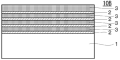
また、図3は、単結晶シリコンウェーハ上に酸素原子層と単結晶シリコン層を交互に複数層積層させたエピタキシャルウェーハ10Bを示した図である。図3に示すように、本発明のエピタキシャルウェーハの製造方法により、単結晶シリコンウェーハ1上に酸素原子層2と単結晶シリコン層3を交互に繰り返し積層させたエピタキシャルウェーハを得ることができる。このときの最上面は単結晶シリコン層である。
FIG. 3 is a diagram showing an
[エピタキシャルウェーハの製造方法]
図1に、本発明に係るエピタキシャルウェーハの製造フローを示す。[Method for producing epitaxial wafer]
FIG. 1 shows a production flow of an epitaxial wafer according to the present invention.
図1のS11の工程は、単結晶シリコンウェーハを準備する工程である。ここで、基板として用いる単結晶シリコンウェーハの製造方法は特に限定されない。CZ法で製造した単結晶シリコンウェーハでも良いし、FZ法で製造した単結晶シリコンウェーハでも良い。また、CZ法及びFZ法により製造された単結晶シリコンウェーハ上に単結晶シリコンをエピタキシャル成長させたエピタキシャルウェーハを用いても良い。 The step of S11 in FIG. 1 is a step of preparing a single crystal silicon wafer. Here, the manufacturing method of the single crystal silicon wafer used as the substrate is not particularly limited. A single crystal silicon wafer manufactured by the CZ method or a single crystal silicon wafer manufactured by the FZ method may be used. Alternatively, an epitaxial wafer obtained by epitaxially growing single crystal silicon on a single crystal silicon wafer manufactured by the CZ method or the FZ method may be used.
図1のS12の工程は、フッ酸(フッ化水素酸)により自然酸化膜を除去する工程である。本発明では、フッ酸により自然酸化膜を除去できれば良く、使用する薬液としてはフッ酸のみでもよく、バッファードフッ酸のような他の成分を含む薬液を用いてもよい。フッ酸の濃度は自然酸化膜を除去できればよく、例えば0.001%以上かつ60%以下とすることができる。フッ酸の温度は10℃以上かつ50℃以下とすることができる。10℃以上であればフッ酸処理後のウェーハに結露が生じることをより効果的に抑制できる。また、温度を50℃以下であれば揮発するフッ酸の量を適切な範囲とできるため安全性を高くできる。 The process of S12 in FIG. 1 is a process of removing the natural oxide film with hydrofluoric acid (hydrofluoric acid). In the present invention, it suffices if the natural oxide film can be removed with hydrofluoric acid, and the chemical solution used may be hydrofluoric acid alone or a chemical solution containing other components such as buffered hydrofluoric acid. The concentration of hydrofluoric acid is sufficient as long as it can remove the natural oxide film, and can be, for example, 0.001% or more and 60% or less. The temperature of hydrofluoric acid can be 10° C. or higher and 50° C. or lower. If the temperature is 10° C. or higher, the occurrence of dew condensation on the wafer after hydrofluoric acid treatment can be more effectively suppressed. Further, if the temperature is 50° C. or less, the amount of volatilized hydrofluoric acid can be set within an appropriate range, so safety can be enhanced.
フッ酸による自然酸化膜の除去処理(洗浄)の時間は撥水性が確認できるまでとすることができるが、例えば、1秒以上かつ1時間以下とすることができる。1秒以上であればより確実に自然酸化膜を除去することができる。また、1時間以下とすることで生産性を維持できる。 The removal treatment (washing) of the natural oxide film with hydrofluoric acid can be performed until the water repellency is confirmed, for example, 1 second or more and 1 hour or less. If the time is 1 second or more, the native oxide film can be removed more reliably. Moreover, productivity can be maintained by making it 1 hour or less.
フッ酸処理(洗浄)はバッチ式の洗浄装置を用いても良いし、枚葉式の洗浄装置を用いても良い。 For the hydrofluoric acid treatment (washing), a batch-type washing apparatus may be used, or a single wafer-type washing apparatus may be used.
また、フッ酸の蒸気を用いて酸化膜を除去してもよい。 Alternatively, the oxide film may be removed using hydrofluoric acid vapor.
図1のS13の工程は、自然酸化膜を除去した単結晶シリコンウェーハの表面に酸素原子層を形成する工程である。単結晶シリコン中で、酸素原子はシリコン原子と最近接のシリコン原子の間のボンドセンター位置で安定となるため、酸素が1原子層存在すると仮定した場合には、酸素の平面濃度は1.36×10¹⁵atoms/cm2となる。酸素の平面濃度が1×1015atoms/cm2の場合、0.74原子層に相当する。The step S13 in FIG. 1 is a step of forming an oxygen atomic layer on the surface of the single crystal silicon wafer from which the natural oxide film has been removed. In single crystal silicon, oxygen atoms are stable at the bond center position between a silicon atom and the nearest silicon atom. ×10 15 atoms/cm 2 . If the planar concentration of oxygen is 1×10 15 atoms/cm 2 , this corresponds to 0.74 atomic layers.
酸素原子層の形成方法は特に限定されない。例えば、自然酸化膜除去後に純水でリンスすることで酸素原子層を形成することができる。純水を用いることで短時間に酸素原子層を形成することができる。 A method for forming the oxygen atomic layer is not particularly limited. For example, an oxygen atomic layer can be formed by rinsing with pure water after removing the natural oxide film. By using pure water, an oxygen atomic layer can be formed in a short time.
純水の温度は10℃以上かつ100℃以下とすることができる。10℃以上であれば、純水リンス後のウェーハに結露が生じることをより効果的に抑制できる。また、温度は水の沸点の100℃以下とすることができる。 The temperature of the pure water can be 10°C or higher and 100°C or lower. If the temperature is 10° C. or higher, it is possible to more effectively suppress dew condensation on the wafer after rinsing with pure water. Also, the temperature can be 100° C. or lower, which is the boiling point of water.
純水でリンスする時間は1秒以上かつ1時間以下とすることができる。1秒以上であればより確実に酸素原子層を形成することができる。また、1時間以下とすることで時間が掛かりすぎるのを防止することができる。 The time for rinsing with pure water can be 1 second or more and 1 hour or less. If the time is 1 second or longer, the oxygen atomic layer can be formed more reliably. In addition, it is possible to prevent it from taking too much time by making it 1 hour or less.
純水リンスは、バッチ式の洗浄装置を用いても良いし、枚葉式の洗浄装置を用いても良い。 Pure water rinsing may be performed using a batch-type cleaning apparatus or a single wafer-type cleaning apparatus.
リンス後の乾燥は大気中で実施してもよいし、不活性ガス雰囲気で実施してもよい。本発明者らの検討によれば、大気中の有機物の量を十分に減らすことで単結晶シリコンのエピタキシャル成長がより安定する。 Drying after rinsing may be performed in the air or in an inert gas atmosphere. According to studies by the present inventors, the epitaxial growth of single crystal silicon is more stable by sufficiently reducing the amount of organic matter in the atmosphere.
また、自然酸化膜除去後に酸素を含む雰囲気中でウェーハを放置することでも、酸素原子層を形成することができる。 An oxygen atomic layer can also be formed by leaving the wafer in an atmosphere containing oxygen after removing the natural oxide film.
純水リンスより酸素雰囲気中の放置の方が緩やかに酸素原子層が形成されるため、酸素を含む雰囲気中に放置することで酸素原子層の酸素濃度を正確に制御することができる。フッ酸により自然酸化膜を除去した後のシリコン基板表面は水素終端されているため、酸素雰囲気中でも容易には酸化されない。酸素原子層の酸素濃度は放置時間及び温度により制御することができる。酸化は室温でも進行するため、熱処理炉に入れて酸化しなくてもよい。単結晶シリコンウェーハにパーティクルが付着してエピタキシャル成長時に欠陥が発生するのを防止するため、ウェーハを放置する環境はクリーンルーム中とすることが望ましい。 Since an oxygen atomic layer is formed more slowly by leaving in an oxygen atmosphere than by rinsing with pure water, the oxygen concentration of the oxygen atomic layer can be accurately controlled by leaving in an oxygen-containing atmosphere. Since the surface of the silicon substrate after removing the native oxide film with hydrofluoric acid is terminated with hydrogen, it is not easily oxidized even in an oxygen atmosphere. The oxygen concentration of the oxygen atomic layer can be controlled by the standing time and temperature. Since oxidation proceeds even at room temperature, it is not necessary to place the substrate in a heat treatment furnace for oxidation. In order to prevent defects from occurring during epitaxial growth due to particles adhering to the single crystal silicon wafer, it is desirable that the environment in which the wafer is left is in a clean room.
さらに、酸素原子層を形成する工程では、自然酸化膜除去後に純水によりリンスする処理と酸素を含む雰囲気中でウェーハを放置する処理とを組み合わせた処理で酸素原子層を形成することができる。純水を用いた短時間での酸素原子層の形成と酸素による緩やかな酸素原子層の形成を組み合わせることで、短時間で精度よく酸素原子層の酸素濃度を制御することができる。 Furthermore, in the step of forming the oxygen atomic layer, the oxygen atomic layer can be formed by a combination of rinsing with pure water after removing the natural oxide film and leaving the wafer in an oxygen-containing atmosphere. By combining the formation of the oxygen atomic layer in a short time using pure water and the gentle formation of the oxygen atomic layer using oxygen, the oxygen concentration of the oxygen atomic layer can be controlled in a short period of time with high accuracy.
図1のS14は単結晶シリコンをエピタキシャル成長させる工程である。成長に使うガスとして、モノシランやジシランを使うことができる。キャリアガスとして窒素や水素を使用しても良い。また、エピタキシャル成長を行うチャンバーの圧力は、気相中で微小シリコン結晶が生じない圧力であればよい。例えば、133Pa以上かつ13300Pa以下の圧力とすることができる。エピタキシャル成長装置としては、バッチ式を使用しても良いし、枚葉式を使用しても良い。 S14 in FIG. 1 is a step of epitaxially growing single crystal silicon. Monosilane or disilane can be used as the gas used for growth. Nitrogen or hydrogen may be used as a carrier gas. Moreover, the pressure of the chamber for epitaxial growth may be any pressure that does not generate micro silicon crystals in the gas phase. For example, the pressure can be 133 Pa or more and 13300 Pa or less. As an epitaxial growth apparatus, a batch type may be used, or a single wafer type may be used.
また、単結晶シリコンのエピタキシャル成長を、450℃以上かつ800℃以下の温度で行うことができる。このような温度で成長を行うことで、エピタキシャル層に転位及び積層欠陥が形成されるのを防止できる。温度が高いほどエピタキシャル成長レートは高くなるため、高温で成膜することで厚いエピタキシャル層を短時間で形成することができる。一方で、薄いエピタキシャル層を形成したい場合には低温で成膜すればよい。このように、目的とするエピタキシャル層の厚さに応じて成長温度を変えることができる。また、エピタキシャル層の厚さを調整するために成膜時間を調整することができる。 Further, epitaxial growth of single crystal silicon can be performed at a temperature of 450° C. or higher and 800° C. or lower. Growth at such a temperature can prevent the formation of dislocations and stacking faults in the epitaxial layer. Since the higher the temperature, the higher the epitaxial growth rate, film formation at a high temperature makes it possible to form a thick epitaxial layer in a short time. On the other hand, if it is desired to form a thin epitaxial layer, the film should be formed at a low temperature. Thus, the growth temperature can be varied according to the desired thickness of the epitaxial layer. Also, the deposition time can be adjusted to adjust the thickness of the epitaxial layer.
なお、単結晶シリコンのエピタキシャル成長を行う場合、通常はエピタキシャル成長の直前に、基板表面の自然酸化膜の除去や清浄化のための水素ベークが行われるが、本発明に係るエピタキシャル成長する工程では、水素ベークを行わず、所定の成長温度に達したところでエピタキシャル成長を開始することが好ましい。酸素原子層の消失を防ぐためである。ここで言う水素ベークとは、水素雰囲気中で単結晶シリコンウェーハを800℃以上で一定時間保持することを意味している。800℃未満では酸素原子層は消失されないので、800℃未満であればエピタキシャル成長前にキャリアガスとして水素を流しても何ら問題はない。 When epitaxial growth of single crystal silicon is performed, hydrogen baking is usually performed immediately before epitaxial growth for removing a natural oxide film on the substrate surface and for cleaning. It is preferable to start the epitaxial growth when the predetermined growth temperature is reached without performing the This is to prevent the disappearance of the oxygen atomic layer. The term "hydrogen baking" as used herein means holding a single crystal silicon wafer at 800° C. or higher in a hydrogen atmosphere for a certain period of time. Since the oxygen atomic layer does not disappear at temperatures below 800° C., there is no problem in flowing hydrogen as a carrier gas before epitaxial growth at temperatures below 800° C.
酸素原子層の酸素の平面濃度を1×10¹⁵atoms/cm2以下とすることで、エピタキシャル層中に欠陥が形成されない。これは、酸化量が少ない場合には基板の結晶性が保たれるためである。このため、酸素の平面濃度の下限値はなく、0よりも大きければよい。酸化量が多く、酸素原子層の酸素の平面濃度が1×1015atoms/cm2より高い場合には、結晶性の高いエピタキシャル層は形成されず多結晶シリコン又はアモルファスシリコンになる。By setting the plane concentration of oxygen in the oxygen atomic layer to 1×10 15 atoms/cm 2 or less, defects are not formed in the epitaxial layer. This is because the crystallinity of the substrate is maintained when the amount of oxidation is small. Therefore, there is no lower limit for the plane concentration of oxygen, and it is sufficient that it is greater than zero. When the amount of oxidation is large and the planar concentration of oxygen in the oxygen atomic layer is higher than 1×10 15 atoms/cm 2 , an epitaxial layer with high crystallinity is not formed and becomes polycrystalline silicon or amorphous silicon.
ここで、酸素の平面濃度は、例えばSIMS(Secondary Ion Mass Spectrometry)により測定することができる。酸化層を含むSiをSIMSで測定した場合には、酸化層が形成された深さに酸素のピークが形成される。ピーク付近において1回のスパッタリングによる体積濃度と深さの積を積算することで、平面濃度を求めることができる。 Here, the planar concentration of oxygen can be measured, for example, by SIMS (Secondary Ion Mass Spectrometry). When Si including an oxide layer is measured by SIMS, an oxygen peak is formed at the depth where the oxide layer is formed. The planar concentration can be obtained by accumulating the product of the volume concentration and the depth due to one sputtering in the vicinity of the peak.
単結晶シリコンウェーハの表面上に酸素原子層を形成する工程と、単結晶シリコンをエピタキシャル成長する工程とを交互に複数回行うことができる。このように酸素原子層を複数層設けることで、単層の場合よりもゲッタリング効果を高めることができる。 The step of forming an oxygen atomic layer on the surface of the single crystal silicon wafer and the step of epitaxially growing single crystal silicon can be alternately performed multiple times. By providing a plurality of oxygen atomic layers in this manner, the gettering effect can be enhanced as compared with the case of a single layer.
以下、実施例を挙げて本発明について詳細に説明するが、これは本発明を限定するものではない。 EXAMPLES The present invention will be described in detail below with reference to examples, but these are not intended to limit the present invention.
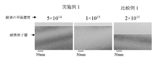
(実施例1、比較例1)
準備した単結晶シリコン基板の導電型、直径、結晶面方位は以下の通りである。
基板の導電型 : p型
直径 : 300mm
結晶面方位 : (100)(Example 1, Comparative Example 1)
The conductivity type, diameter, and crystal plane orientation of the prepared single crystal silicon substrate are as follows.
Substrate conductivity type: p-type Diameter: 300mm
Crystal plane orientation: (100)
次に、準備した単結晶シリコン基板の自然酸化膜を除去するためにバッチ式の装置でフッ酸洗浄後、純水でリンスした。その後、清浄度クラス100の大気中に2~5時間放置した。具体的には、実施例1で2時間及び3時間、比較例1で5時間の放置時間とした。次に、水素ベークを行わずに単結晶シリコンのエピタキシャル成長を行った。このとき、圧力は4000Pa、成長温度は580℃とした。 Next, in order to remove a natural oxide film on the prepared single crystal silicon substrate, the substrate was washed with hydrofluoric acid in a batch type apparatus and then rinsed with pure water. After that, it was left in the atmosphere of cleanliness class 100 for 2 to 5 hours. Specifically, the leaving time was 2 hours and 3 hours in Example 1, and 5 hours in Comparative Example 1. Next, single crystal silicon was epitaxially grown without hydrogen baking. At this time, the pressure was 4000 Pa and the growth temperature was 580°C.
その後、酸素原子層における酸素の平面濃度をSIMSにより測定した。また、結晶性を評価するために断面TEM(Transmission Electron Microscopy)観察を行った。図4に観察結果を示す。 After that, the planar concentration of oxygen in the oxygen atomic layer was measured by SIMS. In addition, cross-sectional TEM (Transmission Electron Microscopy) observation was performed to evaluate the crystallinity. The observation results are shown in FIG.
SIMS測定の結果、実施例1では酸素の平面濃度が5×10¹⁴atoms/cm2及び1×1015atoms/cm2のものが、比較例1では酸素の平面濃度が2×1015atoms/cm2のものが得られたことがわかった。As a result of SIMS measurement, Example 1 had a planar oxygen concentration of 5×10 14 atoms/cm 2 and 1×10 15 atoms/cm 2 , and Comparative Example 1 had a planar oxygen concentration of 2×10 15 atoms/
断面TEM観察の結果(図4)から、実施例1のように酸素の平面濃度が1×10¹⁵atoms/cm2以下では、酸素原子層上に転位及び積層欠陥が形成されることなく単結晶シリコン層が形成できていることがわかる。一方、比較例1のように酸素の平面濃度が2×1015atoms/cm2の場合には、エピタキシャル層が単結晶シリコンではなくアモルファスシリコンとなっている。なお、図4の比較例1の断面TEM観察画像では、画像の上半部全体がアモルファスシリコン層である。この場合、成膜後に熱処理を行うとアモルファスシリコンはポリシリコンとなる。From the results of cross-sectional TEM observation (FIG. 4), when the plane concentration of oxygen is 1×10 15 atoms/cm 2 or less as in Example 1, dislocations and stacking faults are not formed on the oxygen atomic layer, and a single crystal can be formed. It can be seen that a silicon layer has been formed. On the other hand, when the planar concentration of oxygen is 2×10 15 atoms/cm 2 as in Comparative Example 1, the epitaxial layer is not single crystal silicon but amorphous silicon. Note that in the cross-sectional TEM observation image of Comparative Example 1 in FIG. 4, the entire upper half of the image is the amorphous silicon layer. In this case, amorphous silicon becomes polysilicon when heat treatment is performed after film formation.
(実施例2)
実施例1及び比較例1と同じ単結晶シリコン基板を準備した。次に、準備した単結晶シリコン基板の自然酸化膜を除去するために、バッチ式又は枚葉式の装置でフッ酸洗浄を行った後、純水でリンスした。その後、清浄度クラス100の大気中の放置時間が10分以内となるようにして酸素原子層を形成し、続いて水素ベークを行わずに単結晶シリコンのエピタキシャル成長を行った。このとき、圧力は4000Pa、成長温度は580℃とした。(Example 2)
The same single crystal silicon substrates as in Example 1 and Comparative Example 1 were prepared. Next, in order to remove a native oxide film from the prepared single crystal silicon substrate, the substrate was cleaned with hydrofluoric acid using a batch type or single wafer type apparatus, and then rinsed with pure water. After that, an oxygen atomic layer was formed so that the exposure time in the atmosphere of cleanliness class 100 was within 10 minutes, and then epitaxial growth of single crystal silicon was performed without hydrogen baking. At this time, the pressure was 4000 Pa and the growth temperature was 580°C.
その後、酸素原子層における酸素の平面濃度をSIMSにより測定した。その結果、いずれのフッ酸洗浄方式においても、酸素原子層の酸素の平面濃度は1×10¹⁴atoms/cm2であった。After that, the planar concentration of oxygen in the oxygen atomic layer was measured by SIMS. As a result, the planar concentration of oxygen in the oxygen atomic layer was 1×10 14 atoms/cm 2 in both hydrofluoric acid cleaning methods.
さらに、結晶性を評価するために断面TEM観察を行った。図5に観察結果を示す。酸素原子層上に転位及び積層欠陥が形成されることなく単結晶シリコン層が形成できていることがわかる。なお、実施例2のように酸素原子層の酸素の平面濃度が1×10¹⁴atoms/cm2程度になると断面TEM観察画像において酸素原子層のコントラストの変化が弱くなるため、図4の実施例1の断面TEM観察画像と比べて酸素原子層が見えづらくなっているが、SIMS測定で酸素原子層の部分に明確な酸素のピークが観察され酸素原子層の存在は確認できている。Furthermore, cross-sectional TEM observation was performed to evaluate the crystallinity. The observation results are shown in FIG. It can be seen that a single crystal silicon layer was formed on the oxygen atomic layer without formation of dislocations and stacking faults. Note that when the planar concentration of oxygen in the oxygen atomic layer is about 1×10 14 atoms/cm 2 as in Example 2, the change in contrast of the oxygen atomic layer in the cross-sectional TEM observation image becomes weak. Compared to the cross-sectional TEM observation image of 1, the oxygen atomic layer is difficult to see, but SIMS measurement shows a clear oxygen peak in the oxygen atomic layer portion, confirming the existence of the oxygen atomic layer.
本発明に係るエピタキシャルウェーハの製造方法であれば、酸素原子層をエピタキシャル層に安定的かつ簡便に導入することができるとともに、良質な単結晶シリコンのエピタキシャル層を有するエピタキシャルウェーハを得ることが可能となる。 With the epitaxial wafer manufacturing method according to the present invention, an oxygen atomic layer can be stably and easily introduced into the epitaxial layer, and an epitaxial wafer having an epitaxial layer of high-quality single crystal silicon can be obtained. Become.
なお、本発明は、上記実施形態に限定されるものではない。上記実施形態は例示であり、本発明の特許請求の範囲に記載された技術的思想と実質的に同一な構成を有し、同様な作用効果を奏するものは、いかなるものであっても本発明の技術的範囲に包含される。 It should be noted that the present invention is not limited to the above embodiments. The above-described embodiment is an example, and any device having substantially the same configuration as the technical idea described in the claims of the present invention and exhibiting the same effect is the present invention. included in the technical scope of
Claims (3)
フッ酸により前記単結晶シリコンウェーハ表面の自然酸化膜を除去する工程、
前記自然酸化膜を除去した前記単結晶シリコンウェーハの表面に酸素原子層を形成する工程、
前記酸素原子層を形成した前記単結晶シリコンウェーハの表面上に気相成長法により前記単結晶シリコン層をエピタキシャル成長する工程を含み、
前記酸素原子層の酸素の平面濃度を1×10¹⁵atoms/cm2以下とし、
前記酸素原子層を形成する工程では、前記単結晶シリコンウェーハを純水によりリンスすること、及び、酸素を含む雰囲気中に前記単結晶シリコンウェーハを放置することで、前記酸素原子層を形成することを特徴とするエピタキシャルウェーハの製造方法。 An epitaxial wafer manufacturing method for forming a single crystal silicon layer on a single crystal silicon wafer,
removing a natural oxide film on the surface of the single crystal silicon wafer with hydrofluoric acid;
forming an oxygen atomic layer on the surface of the single crystal silicon wafer from which the native oxide film has been removed;
A step of epitaxially growing the single crystal silicon layer on the surface of the single crystal silicon wafer on which the oxygen atomic layer is formed by vapor phase epitaxy ;
The planar concentration of oxygen in the oxygen atomic layer is set to 1×10 15 atoms/cm 2 or less,
In the step of forming the oxygen atomic layer, the oxygen atomic layer is formed by rinsing the single crystal silicon wafer with pure water and leaving the single crystal silicon wafer in an atmosphere containing oxygen. A method for producing an epitaxial wafer, characterized by:
Applications Claiming Priority (3)
| Application Number | Priority Date | Filing Date | Title |
|---|---|---|---|
| JP2021009549 | 2021-01-25 | ||
| JP2021009549 | 2021-01-25 | ||
| PCT/JP2021/044763 WO2022158148A1 (en) | 2021-01-25 | 2021-12-06 | Method for manufacturing epitaxial wafer |
Publications (3)
| Publication Number | Publication Date |
|---|---|
| JPWO2022158148A1 JPWO2022158148A1 (en) | 2022-07-28 |
| JPWO2022158148A5 JPWO2022158148A5 (en) | 2022-12-23 |
| JP7231120B2 true JP7231120B2 (en) | 2023-03-01 |
Family
ID=82549737
Family Applications (1)
| Application Number | Title | Priority Date | Filing Date |
|---|---|---|---|
| JP2022552294A Active JP7231120B2 (en) | 2021-01-25 | 2021-12-06 | Epitaxial wafer manufacturing method |
Country Status (7)
| Country | Link |
|---|---|
| US (1) | US20240063027A1 (en) |
| EP (1) | EP4283024A1 (en) |
| JP (1) | JP7231120B2 (en) |
| KR (1) | KR20230132455A (en) |
| CN (1) | CN116685723A (en) |
| TW (1) | TW202230462A (en) |
| WO (1) | WO2022158148A1 (en) |
Families Citing this family (1)
| Publication number | Priority date | Publication date | Assignee | Title |
|---|---|---|---|---|
| JP7435516B2 (en) | 2021-03-22 | 2024-02-21 | 信越半導体株式会社 | Epitaxial wafer manufacturing method |
Citations (4)
| Publication number | Priority date | Publication date | Assignee | Title |
|---|---|---|---|---|
| JP2000323689A (en) | 1999-05-14 | 2000-11-24 | Toshiba Corp | Semiconductor epitaxial substrate and its manufacture |
| JP2003197549A (en) | 2002-09-06 | 2003-07-11 | Sumitomo Mitsubishi Silicon Corp | Method of manufacturing epitaxial wafer |
| JP2014165494A (en) | 2013-02-22 | 2014-09-08 | Imec | Oxygen monolayer on semiconductor |
| JP2019004050A (en) | 2017-06-15 | 2019-01-10 | 信越半導体株式会社 | Manufacturing method of epitaxial wafer |
Family Cites Families (5)
| Publication number | Priority date | Publication date | Assignee | Title |
|---|---|---|---|---|
| US5422306A (en) | 1991-12-17 | 1995-06-06 | Matsushita Electric Industrial Co., Ltd. | Method of forming semiconductor hetero interfaces |
| WO2005018005A1 (en) | 2003-06-26 | 2005-02-24 | Rj Mears, Llc | Semiconductor device including mosfet having band-engineered superlattice |
| US7153763B2 (en) | 2003-06-26 | 2006-12-26 | Rj Mears, Llc | Method for making a semiconductor device including band-engineered superlattice using intermediate annealing |
| JP5168990B2 (en) | 2007-04-11 | 2013-03-27 | 信越半導体株式会社 | Manufacturing method of semiconductor substrate |
| JP5205840B2 (en) | 2007-07-06 | 2013-06-05 | 信越半導体株式会社 | Manufacturing method of semiconductor substrate |
-
2021
- 2021-12-06 CN CN202180088195.8A patent/CN116685723A/en active Pending
- 2021-12-06 WO PCT/JP2021/044763 patent/WO2022158148A1/en active Application Filing
- 2021-12-06 US US18/269,646 patent/US20240063027A1/en active Pending
- 2021-12-06 KR KR1020237023432A patent/KR20230132455A/en unknown
- 2021-12-06 JP JP2022552294A patent/JP7231120B2/en active Active
- 2021-12-06 EP EP21921250.3A patent/EP4283024A1/en active Pending
- 2021-12-09 TW TW110145970A patent/TW202230462A/en unknown
Patent Citations (4)
| Publication number | Priority date | Publication date | Assignee | Title |
|---|---|---|---|---|
| JP2000323689A (en) | 1999-05-14 | 2000-11-24 | Toshiba Corp | Semiconductor epitaxial substrate and its manufacture |
| JP2003197549A (en) | 2002-09-06 | 2003-07-11 | Sumitomo Mitsubishi Silicon Corp | Method of manufacturing epitaxial wafer |
| JP2014165494A (en) | 2013-02-22 | 2014-09-08 | Imec | Oxygen monolayer on semiconductor |
| JP2019004050A (en) | 2017-06-15 | 2019-01-10 | 信越半導体株式会社 | Manufacturing method of epitaxial wafer |
Also Published As
| Publication number | Publication date |
|---|---|
| US20240063027A1 (en) | 2024-02-22 |
| TW202230462A (en) | 2022-08-01 |
| EP4283024A1 (en) | 2023-11-29 |
| CN116685723A (en) | 2023-09-01 |
| KR20230132455A (en) | 2023-09-15 |
| WO2022158148A1 (en) | 2022-07-28 |
| JPWO2022158148A1 (en) | 2022-07-28 |
Similar Documents
| Publication | Publication Date | Title |
|---|---|---|
| JP5015134B2 (en) | Method for removing oxides from a substrate | |
| TWI382456B (en) | Epitaxial growth of relaxed silicon germanium layers | |
| JP7231120B2 (en) | Epitaxial wafer manufacturing method | |
| JPH09199416A (en) | Semiconductor substrate and manufacture thereof | |
| JP2010034330A (en) | Epitaxial wafer and method of manufacturing the same | |
| JP5246065B2 (en) | Epitaxial silicon wafer and manufacturing method thereof | |
| JP5609025B2 (en) | Epitaxial silicon wafer manufacturing method | |
| WO2021140763A1 (en) | Epitaxial wafer manufacturing method and epitaxial wafer | |
| JP2022125625A (en) | Manufacturing method for epitaxial wafer | |
| JP7435516B2 (en) | Epitaxial wafer manufacturing method | |
| JP2001210650A (en) | Method for manufacturing epitaxial silicon wafer | |
| JPH1140506A (en) | Manufacture of epitaxial wafer | |
| WO2011007678A1 (en) | Epitaxial silicon wafer and method for manufacturing same | |
| JP7347350B2 (en) | Method for setting epitaxial growth conditions and method for manufacturing epitaxial wafers | |
| JP4120163B2 (en) | Si epitaxial wafer manufacturing method and Si epitaxial wafer | |
| WO2024009705A1 (en) | Method for manufacturing epitaxial wafer | |
| JP3922674B2 (en) | Silicon wafer manufacturing method | |
| JP2003188107A (en) | Manufacturing method for semiconductor epitaxial wafer and the semiconductor epitaxial wafer | |
| CN110998789A (en) | Semiconductor wafer of monocrystalline silicon and method for producing a semiconductor wafer | |
| JPH0660401B2 (en) | Silicon thin film manufacturing method | |
| JP2010062219A (en) | Production process of silicon carbide | |
| TW202344699A (en) | Production method for single crystal semiconductor film, production method for multilayer film of single crystal semiconductor film, and semiconductor element | |
| TW525215B (en) | Method of improving exipaxy wafer quality | |
| JPH05211123A (en) | Growth method of silicon epitaxial film | |
| CN117672815A (en) | SiC epitaxial wafer and preparation method thereof |
Legal Events
| Date | Code | Title | Description |
|---|---|---|---|
| A521 | Request for written amendment filed |
Free format text: JAPANESE INTERMEDIATE CODE: A523 Effective date: 20220829 |
|
| A621 | Written request for application examination |
Free format text: JAPANESE INTERMEDIATE CODE: A621 Effective date: 20220829 |
|
| A871 | Explanation of circumstances concerning accelerated examination |
Free format text: JAPANESE INTERMEDIATE CODE: A871 Effective date: 20220829 |
|
| A131 | Notification of reasons for refusal |
Free format text: JAPANESE INTERMEDIATE CODE: A131 Effective date: 20220913 |
|
| A521 | Request for written amendment filed |
Free format text: JAPANESE INTERMEDIATE CODE: A523 Effective date: 20221102 |
|
| TRDD | Decision of grant or rejection written | ||
| A01 | Written decision to grant a patent or to grant a registration (utility model) |
Free format text: JAPANESE INTERMEDIATE CODE: A01 Effective date: 20230117 |
|
| A61 | First payment of annual fees (during grant procedure) |
Free format text: JAPANESE INTERMEDIATE CODE: A61 Effective date: 20230130 |
|
| R150 | Certificate of patent or registration of utility model |
Ref document number: 7231120 Country of ref document: JP Free format text: JAPANESE INTERMEDIATE CODE: R150 |