JP7219084B2 - capacitor - Google Patents
capacitor Download PDFInfo
- Publication number
- JP7219084B2 JP7219084B2 JP2018244261A JP2018244261A JP7219084B2 JP 7219084 B2 JP7219084 B2 JP 7219084B2 JP 2018244261 A JP2018244261 A JP 2018244261A JP 2018244261 A JP2018244261 A JP 2018244261A JP 7219084 B2 JP7219084 B2 JP 7219084B2
- Authority
- JP
- Japan
- Prior art keywords
- tape
- capacitor
- fixing tape
- capacitor element
- wound
- Prior art date
- Legal status (The legal status is an assumption and is not a legal conclusion. Google has not performed a legal analysis and makes no representation as to the accuracy of the status listed.)
- Active
Links
Images


Landscapes
- Fixed Capacitors And Capacitor Manufacturing Machines (AREA)
Description
本発明は、コンデンサに関し、特に、電極箔を巻き折りまたは巻回してなるコンデンサ素子を有する電解コンデンサに関する。 TECHNICAL FIELD The present invention relates to a capacitor, and more particularly to an electrolytic capacitor having a capacitor element formed by folding or winding an electrode foil.
従来、この種の技術としては、特許文献1に記載された技術がある。特許文献1には、陰極箔とセパレータ(電解紙)とを積層して九十九折りし、各セパレータの間に陽極箔を配置したコンデンサ素子を有する電解コンデンサにおいて、陰極箔又はセパレータの少なくともどちらか一方の折り曲げ部分に、ミシン目を設ける電解コンデンサについて開示されている。
Conventionally, there is a technique described in
ところで、このような構成の電解コンデンサでは、陰極箔及び陽極箔と電解液を含浸したセパレータとの密着性が低下し易く、低周波領域での等価直列抵抗(ESR)が高くなる傾向がある。このため、陰極箔及び陽極箔と電解液を含浸したセパレータとの密着性を高くして、その状態を維持する必要がある。 By the way, in the electrolytic capacitor having such a structure, the adhesion between the cathode foil and the anode foil and the separator impregnated with the electrolytic solution tends to deteriorate, and the equivalent series resistance (ESR) tends to increase in the low frequency region. For this reason, it is necessary to increase the adhesion between the cathode foil, the anode foil, and the separator impregnated with the electrolytic solution, and maintain this state.
ここで、陰極箔及び陽極箔とセパレータとの密着性を高くする方法として、セパレータに素子止めテープを貼着してセパレータの先端部を固定する際に、素子止めテープにテンションをかけながら素子止めテープを貼着することが考えられる。 Here, as a method for increasing the adhesion between the cathode foil and the anode foil and the separator, when the element-fixing tape is attached to the separator and the tip of the separator is fixed, the element-fixing tape is applied with tension. It is conceivable to apply tape.
この方法では、テンションをかけながらコンデンサ素子を折り込むために、それに適した材質の素子止めテープを選択するが、時間の経過とともに素子止めテープの熱収縮が起こり、それに伴う接着力の低下によりコンデンサ素子にスプリングバックによる素子膨れが生じる問題があった。特に高温環境下で使用される電解コンデンサでこのような事象が大きな問題となっていた。 In this method, since the capacitor element is folded while applying tension, the element fixing tape made of suitable material is selected. However, there is a problem that element swelling occurs due to springback. In particular, such a phenomenon has become a serious problem in electrolytic capacitors used in high-temperature environments.
また、電極箔(陽極箔および陰極箔)をセパレータを挟んで所定の巻回方向に巻回し、巻き終わりを素子止めテープにより止めることにより製造される巻回形のコンデンサ素子を有する電解コンデンサにおいても、同様にコンデンサ素子にスプリングバックによる素子膨れが生じる問題があった。 Also in an electrolytic capacitor having a wound capacitor element manufactured by winding electrode foils (anode foil and cathode foil) with a separator in between in a predetermined winding direction and stopping the winding end with an element fixing tape. Similarly, there is a problem that the capacitor element swells due to springback.
この点について、従来、二次電池の分野では、例えば特許文献2に開示されているように、素子止めテープを偏平巻電極の縦方向および横方向に設けることにより、偏平巻電極の巻き終わり部の緩みを防止するとともに、高温放置後の容量回復率を向上させるものが知られている。
Regarding this point, conventionally, in the field of secondary batteries, for example, as disclosed in
しかしながら、二次電池の使用環境温度として想定される温度は、電解コンデンサに求められる温度環境よりも低い温度条件となっており、一段と高い温度環境下での使用が想定される電解コンデンサとしては、さらなる対策を講じる必要があった。 However, the temperature assumed as the operating environment temperature for secondary batteries is lower than the temperature environment required for electrolytic capacitors. Further measures had to be taken.
本発明は、以上の点を考慮してなされたものであり、高温環境下で使用した場合であっても、コンデンサ素子にスプリングバックによる素子膨れが発生することを抑止し得るコンデンサを提供することを目的とするものである。 SUMMARY OF THE INVENTION The present invention has been made in view of the above points, and provides a capacitor capable of suppressing swelling of the capacitor element due to springback even when used in a high-temperature environment. It is intended for
本発明のコンデンサは、陰極箔および陽極箔がセパレータを介して積層される積層体を巻き折りまたは巻回されてなるコンデンサ素子と、前記コンデンサ素子に対して、前記積層体の巻き折り方向または巻回方向に巻回される第1の素子止めテープと、前記コンデンサ素子に対して巻回され、前記第1の素子止めテープと材質が異なる第2の素子止めテープと、を備え、前記第2の素子止めテープは、前記第1の素子止めテープと比較して耐熱性が高く、前記第1の素子止めテープは、前記第2の素子止めテープと比較して伸び率が高いことを特徴とする。 The capacitor of the present invention comprises a capacitor element obtained by winding or winding a laminate in which a cathode foil and an anode foil are laminated with a separator interposed therebetween; a first element-fixing tape wound in a winding direction; and a second element-fixing tape wound around the capacitor element and made of a material different from that of the first element-fixing tape, wherein the second The element-fixing tape has higher heat resistance than the first element-fixing tape, and the first element-fixing tape has a higher elongation rate than the second element-fixing tape. do.
この構成によれば、相対的に伸び率が高い第1の素子止めテープがコンデンサ素子の巻き折りまたは巻回方向に巻回されているので、第1の素子止めテープを巻き折りまたは巻回方向にテンションを掛けながら巻回することができるので、素子厚を小さくするともに陽極箔と陰極箔とをセパレータを介して近接させることによりESRを低減することができる。一方、高温環境下で第1の素子止めテープに巻き緩みが発生した場合でも、相対的に耐熱性が高い第2の素子止めテープがコンデンサ素子に巻回されているので、高温環境下における素子止めテープの熱収縮に起因する接着力の低下を抑制し、素子膨れを抑止することができる。 According to this configuration, since the first element-fixing tape having a relatively high elongation rate is wound in the winding-folding or winding direction of the capacitor element, the first element-fixing tape is wound in the winding-folding or winding direction. ESR can be reduced by making the element thickness smaller and bringing the anode foil and the cathode foil close to each other with the separator interposed therebetween. On the other hand, even if the first element-fixing tape becomes loose in a high-temperature environment, the second element-fixing tape, which has relatively high heat resistance, is wound around the capacitor element, so that the element can be It is possible to suppress the deterioration of the adhesive force due to the thermal shrinkage of the fastening tape, and suppress the swelling of the element.
また、本発明のコンデンサは、上記構成において、電解液を含浸した前記コンデンサ素子を収納する有底形状の外装ケースと、前記外装ケースの開口端を封口するとともに前記コンデンサ素子に接続された前記引き出しリード線が挿通される挿通孔を有する封口体と、をさらに備え、前記コンデンサ素子は、前記積層体として、2枚の帯状の前記セパレータと、前記2枚のセパレータの間に挟まれた帯状の前記陰極箔と、前記2枚のセパレータと前記陰極箔とが巻き折られて形成される隣合う区画の間に前記セパレータに挟まれた状態で配置された短冊状の前記陽極箔とを有し、前記第1の素子止めテープは前記積層体の巻き折り方向に巻回されることを特徴とする。 In the above configuration, the capacitor of the present invention has a bottomed exterior case that houses the capacitor element impregnated with the electrolytic solution, and the drawer that seals an open end of the exterior case and is connected to the capacitor element. a sealing member having an insertion hole through which a lead wire is inserted, and the capacitor element includes, as the laminate, two strip-shaped separators and a strip-shaped separator sandwiched between the two separators. The cathode foil, and the strip-shaped anode foil sandwiched between the separators between adjacent sections formed by winding and folding the two sheets of the separator and the cathode foil. , wherein the first element fixing tape is wound in a winding direction of the laminate.
この構成によれば、2枚の帯状のセパレータと、帯状の前記陰極箔と、短冊状の陽極箔とを有し、2枚のセパレータの間に陰極箔を挟んでなる積層体を巻き折りし、当該巻き折りによって形成される隣合う区画の間に陽極箔を介在させてなるコンデンサ素子を有する積層形のコンデンサにおいて、高温度環境下で使用した場合であっても、第2の素子止めテープの耐熱性により、コンデンサ素子にスプリングバックによる素子膨れが発生することを抑止することができる。
また、2枚のセパレータの間に陰極箔を挟んでなる積層体を巻き折りする構成としたことにより、セパレータのスプリングバックを軽減することができる。
According to this configuration, a laminate having two strip-shaped separators, a strip-shaped cathode foil, and a strip-shaped anode foil, and having the cathode foil sandwiched between the two separators is rolled and folded. , in a laminated capacitor having a capacitor element in which anode foil is interposed between adjacent sections formed by said winding and folding, even when used in a high temperature environment, the second element fixing tape Due to the heat resistance of , it is possible to suppress the occurrence of swelling of the capacitor element due to springback.
In addition, the springback of the separator can be reduced by adopting the configuration in which the laminate formed by sandwiching the cathode foil between the two separators is folded.
また、本発明のコンデンサは、上記構成において、電解液を含浸した前記コンデンサ素子を収納する有底形状の外装ケースと、前記外装ケースの開口端を封口するとともに前記コンデンサ素子に接続された前記引き出しリード線が挿通される挿通孔を有する封口体と、をさらに備え、前記コンデンサ素子は、前記積層体として、それぞれ帯状の前記セパレータ、前記陰極箔および前記陽極箔が所定の巻回方向に巻回されてなり、前記第1の素子止めテープは前記積層体の巻回方向に巻回されることを特徴とする。 In the above configuration, the capacitor of the present invention has a bottomed exterior case that houses the capacitor element impregnated with the electrolytic solution, and the drawer that seals an open end of the exterior case and is connected to the capacitor element. and a sealing member having an insertion hole through which a lead wire is inserted, wherein the capacitor element is formed by winding the strip-shaped separator, the cathode foil, and the anode foil as the laminated body in a predetermined winding direction. and the first element fixing tape is wound in the winding direction of the laminate.
この構成によれば、各々に引き出しリード線が接続された前記陽極箔および前記陰極箔が前記セパレータを介して巻回されてなるコンデンサ素子を有する巻回形のコンデンサにおいて、高温度環境下で使用した場合であっても、第2の素子止めテープの耐熱性により、コンデンサ素子にスプリングバックによる素子膨れが発生することを抑止することができる。 According to this configuration, the wound capacitor having the capacitor element formed by winding the anode foil and the cathode foil, to which lead wires are connected respectively, with the separator interposed therebetween, is used in a high-temperature environment. Even in this case, the heat resistance of the second element fixing tape can prevent the capacitor element from swelling due to springback.
また、本発明のコンデンサは、上記構成において、前記第2の素子止めテープは、前記第1の素子止めテープに対して略直交する方向に巻回されていることを特徴とする。 Also, in the capacitor of the present invention having the above structure, the second element-fixing tape is wound in a direction substantially orthogonal to the first element-fixing tape.
この構成によれば、コンデンサ素子に接続された引き出しリード線の近傍に耐熱性の高い第2の素子止めテープを巻回することで、高温によるコンデンサ素子の素子膨れを有効に抑制することができる。 According to this configuration, by winding the second element-fixing tape with high heat resistance in the vicinity of the lead wire connected to the capacitor element, it is possible to effectively suppress element swelling of the capacitor element due to high temperature. .
本発明のコンデンサによると、高温環境下で使用した場合であっても、コンデンサ素子にスプリングバックによる素子膨れが発生することを抑止し得るコンデンサを提供することができる。 ADVANTAGE OF THE INVENTION According to the capacitor of the present invention, it is possible to provide a capacitor capable of suppressing swelling of the capacitor element due to springback even when used in a high-temperature environment.
以下、本発明の実施形態について、図面を参照しながら詳細に説明する。 BEST MODE FOR CARRYING OUT THE INVENTION Hereinafter, embodiments of the present invention will be described in detail with reference to the drawings.
[第1の実施形態]
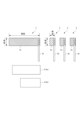
図1は本発明の第1実施形態における積層形の電解コンデンサ1の概観を示す斜視図である。図2は本発明の第1の実施形態における電解コンデンサ1の内部の要部構成を示す説明図である。
[First embodiment]
FIG. 1 is a perspective view showing an overview of a laminated
(電解コンデンサの構成)
図1及び図2に示すように、電解コンデンサ1は、コンデンサ素子10と、ケース21と、封口体22と、リード線23、24と、を備えている。
(Structure of electrolytic capacitor)
As shown in FIGS. 1 and 2, the
コンデンサ素子10(図2参照)は、静電容量により電荷を蓄えたり、放出したりする素子であり、ケース21の内部に収容される。
ケース21は、外形が略直方体形状の有底の筒体からなり、略直方体形状における長手方向の一端側が開放されており、他端側が閉鎖されている。
Capacitor element 10 (see FIG. 2) is an element that stores and releases electric charge by electrostatic capacitance, and is housed inside
The
封口体22は、ケース21の開口を封止する部材であり、本体部22aと、ケース21の開口に挿入される挿入部22bと、を備えている。本体部22aは、略直方体形状であり、本体部22aを挿入方向視した形状は、ケース21を長手方向視した外形と同一である。挿入部22bは、本体部22aの上面から突出しており、挿入部22bの外周は、本体部22aの外周よりも一回り小さく形成されている。このため、本体部22aから挿入部22bにかけて段差が形成されている。ケース21に挿入部22bが挿入された場合に、ケース21の側面と本体部22aの側面とがほぼ面一となる。
The sealing
リード線23、24は、コンデンサ素子10と外部の電気回路とを電気的に接続する端子であり、封口体22に並べて固定されている。リード線23、24の一端部は、本体部22aの底面からケース21の長手方向に沿って延びており、リード線23、24の他端部は、挿入部22bの上面からケース21の長手方向に沿って延びており、リード線23、24の中央部は封口体22に埋設されている。
The
リード線23、24は、コンデンサ素子10の陽極タブ2b、陰極タブ3bに接続される。具体的には、挿入部22bの上面から延びるリード線23に対してコンデンサ素子10の陽極タブ2bが、リード線24に対してコンデンサ素子10の陰極タブ3bが、例えば、溶接によってそれぞれ固定されるとともに、電気的に接続される。
そして、コンデンサ素子10を電解液に浸した後、コンデンサ素子10をケース21内に挿入して、ケース21の開口を封口体22によって封止した後、封口体22の段差部位をレーザー溶接によってケース21に封口体22を完全気密封止することにより、電解コンデンサ1が構成される。
After the
(コンデンサ素子の構成)
次に、コンデンサ素子10について説明する。
図3は、コンデンサ素子10の構成部品を示す説明図である。
図3に示すように、コンデンサ素子10は、複数の陽極部2と、陰極部3と、複数のセパレータ4とを有している。
(Structure of Capacitor Element)
Next,
FIG. 3 is an explanatory diagram showing components of the
As shown in FIG. 3 ,
陽極部2は、陽極箔2aと、陽極タブ2bとを備えている。陰極部3は、陰極箔3aと、陰極タブ3bとを備えている。陽極箔2aは、アルミニウム等の弁作用金属で形成された短冊状の電極(横幅は陰極箔に比べて短い)であり、陽極箔2aの表面はエッチング処理により粗面化されるとともに酸化皮膜が形成されている。陰極箔3aは、陽極箔2aと同様にアルミニウム等の弁作用金属で形成された長尺の帯状の電極である。すなわち、陽極箔2a及び陰極箔3aは矩形であって、タブ取付方向の長さが同一である。なお、以下の説明の便宜上、陰極箔3aの矩形において、タブ取付方向に対して垂直方向に延びる幅を横幅と称し、タブ取付方向に延びる幅を縦幅と称することにする。すなわち、陽極箔2aの縦幅と陰極箔3aの縦幅とは同一である。
The
陽極タブ2bの一端部は、陽極箔2aにおける横幅方向の一端側に固定されており、陽極タブ2bの他端部は、陽極箔2aから縦幅方向に延びている。陰極タブ3bの一端部は、陰極箔3aにおける横幅方向の一端側に固定されており、陰極タブ3bの他端部は、陰極箔3aから縦幅方向に延びている。すなわち、陽極箔2a及び陰極箔3aは、陽極タブ2b及び陰極タブ3bにそれぞれ旗のように固定される。なお、陽極タブ2bは、ケース21の内壁との間でショートが起こりにくくなるように、陽極箔2aの横幅方向の一端部から離れた位置に固定することが望ましい。
One end of
セパレータ4は、横幅が陰極箔3aよりも短く、縦幅が陰極箔3aよりも若干長い矩形の帯状の電解紙であり、その両面には駆動用電解液が含浸および/または固体電解質が形成されている。本実施形態によれば、3枚の陽極箔2aと2枚のセパレータを使用しており、一方のセパレータ4(以下、セパレータ4aと称する)は、他方のセパレータ4(以下、セパレータ4bと称する)よりも横幅が長く設定されている。セパレータ4aは、陽極箔2aの横幅の4倍よりも若干長く、セパレータ4bは、陽極箔2aの横幅の2倍よりも若干長く設定されている。
The
図4は、コンデンサ素子10の構造を示す模式図である。図4に示すように、コンデンサ素子10は、陰極箔3aをセパレータ4a、4bによって挟んでなる積層体7を、巻き折りし(九十九折りと異なり同一方向に折り重ねて)、この巻き折りによって形成された厚み方向に隣合う矩形の区画7a、7aの間に陽極箔2aを介在させた構造を備えている。ここで、陰極箔3aの最外周には、露出部3cが形成されている。本実施形態においては、陰極箔3aの最外周全体がコンデンサ素子10の露出部3cとなる。そして、素子止めテープ6aが外部に露出している陰極箔3aに対して直接貼着されることによって、積層体7の巻き折り構造が維持される。
FIG. 4 is a schematic diagram showing the structure of the
すなわち、図5に示すように、外部に露出している陰極箔3aを巻き折りし(図5(a)、(b))、この状態において、陰極箔3aの端部3dに素子止めテープ6aを貼着し、当該素子止めテープ6aを引っ張って陰極箔3aに張力をかけながら、当該素子止めテープ6aを、剥き出し状態の陰極箔3aの周囲に貼着する。本実施形態においては、1周を若干超えた分だけ素子止めテープ6aを巻き付ける。これにより、素子止めテープ6aによって張力がかけられた状態でコンデンサ素子10が組み立てられる。
That is, as shown in FIG. 5, the
そして、図6に示すように、コンデンサ素子10には、上述のように素子の巻き折り方向に巻き付けられた第1の素子止めテープ6aに加えて、当該素子止めテープ6aと略直交する方向に第2の素子止めテープ6bが巻き付けられて、コンデンサ素子10が完成する。
Then, as shown in FIG. 6, the
以下、コンデンサ素子10の素子止めテープ6a、6bについて説明する。
本実施形態の場合、コンデンサ素子10に対して陰極箔3aの巻き折り方向である横方向に巻回される素子止めテープ6aは、PP(ポリプロピレン)粘着テープ(以下、単にPPテープと呼ぶ)であり、当該素子止めテープ6aに対して直交する方向(縦方向)に巻回される素子止めテープ6bは、PPS(ポリフェニレンサルファイド)粘着テープ(以下、単にPPSテープと呼ぶ)である。
The
In the case of this embodiment, the element-fixing
PPテープは、ポリプロピレンフィルムを基材とし、その片面に接着剤が配置されたものである。PPSテープは、ポリフェニレンサルファイドフィルムを基材とし、その片面に接着剤が配置されたものである。 The PP tape has a polypropylene film as a base material and an adhesive is placed on one side of the film. The PPS tape has a polyphenylene sulfide film as a base material, and an adhesive is arranged on one side thereof.
両テープの性質を比較すると、PPテープは、PPSテープと比較してテープの伸び率が高い。従って、コンデンサ素子2の製造工程において、陽極箔2aおよびセパレータ4を巻き込みながら陰極箔3aを巻き折りする際に、当該陰極箔3aに対して、テンションを掛けながら巻回し、巻き止めることが容易にできる。すなわち、製造上、コンデンサ素子10の巻き折り及び巻止めを容易に行うことができる。
Comparing the properties of both tapes, the PP tape has a higher tape elongation than the PPS tape. Therefore, in the manufacturing process of the
一方、コンデンサ素子10に対してその縦方向に巻回されるPPSテープは、PPテープと比較して耐熱性に優れている。従って、コンデンサ素子10(電解コンデンサ1)が高温の環境下で使用された場合、PPSテープが用いられる素子止めテープ6bにおいては、テープの熱収縮による接着剤の特性劣化に起因する接着力の低下を抑えることができる。これにより、コンデンサ素子10(電解コンデンサ1)の使用環境が、PPSテープに比べて耐熱性の低いPPテープ(素子止めテープ6a)に熱収縮が発生し当該熱収縮により接着力の低下が生じる程度の高温となった場合においても、PPSテープ(素子止めテープ6b)の熱収縮が抑えられた状態が維持されることにより、コンデンサ素子10の高温下における素子膨れの発生を抑制することができる。
On the other hand, the PPS tape wound in the vertical direction around the
特に、コンデンサ素子10においては、陽極タブ2bおよび陰極タブ3bの近傍では熱が発生しやすいが、当該陽極タブ2bおよび陰極タブ3bの近傍に巻回される素子止めテープ6bとしてPPSテープを用いることにより、高温によるテープの熱収縮などの特性劣化を抑制し、素子膨れの発生を抑えることができる。
In particular, in the
以上の構成において、電解コンデンサ1の製造工程において、陰極箔3aを陽極箔2aおよびセパレータ4を巻き込みながら巻き折りする場合、巻き終わり部分に対して素子止めテープ6aとして伸び率の高いPPテープを用い、コンデンサ素子10にテンションを掛けながら巻き取る。この場合、PPテープの伸び率が高い分、テンションをかけ易くなる。これにより、巻回されたコンデンサ素子10の厚みを薄くすることができる。
In the manufacturing process of the
このようにして製造されたコンデンサ素子10を有する電解コンデンサ1を高温環境下で使用する場合、PPテープの耐熱性が低い分、当該PPテープに熱収縮が発生し、当該PPテープとコンデンサ素子10との間の接着力が低下するが、この状態においても、コンデンサ素子10に巻回されたPPSテープの耐熱性がPPテープに比べて高いことにより、PPテープの熱収縮による接着力の低下を抑制できる。これにより、PPテープに熱収縮が発生する温度環境下においても、PPSテープにより巻回されている分、コンデンサ素子2に素子膨れが発生することを抑制することができる。
When the
[製造工程]
次に、電解コンデンサ1の製造工程について図7に示すフローチャートを用いて説明する。
(加締・巻取工程)
陽極タブ2b、陰極タブ3bと電極箔(陽極箔2a、陰極箔3a)とを加締接続するとともに、陰極箔3aを陽極箔2aおよびセパレータ4を巻き込みながら巻き折りすることにより、陽極タブ2b、陰極タブ3bが引き出されたコンデンサ素子10を作製する(ステップS101)。この巻取工程においては、陰極箔3aを巻き折りする際にその巻き終わり部分(陰極箔3aの端部3d)に素子止めテープ6aを貼着しテンションを掛けながら巻き取ることで、コンデンサ素子10の厚みD(図4)を薄くすることができる。第1の素子止めテープ6aを巻回した後、当該素子止めテープ6aに対して略直交する方向に第2の素子止めテープ6bを巻回する。この素子止めテープ6bは、陽極タブ2bおよび陰極タブ3bの間を通して縦方向に巻回される。
[Manufacturing process]
Next, the manufacturing process of the
(Crimping and winding process)
(含浸工程)
減圧や加圧等によりコンデンサ素子10に駆動用電解液を含浸させる(ステップS102)。この時の含浸時間は、コンデンサ素子10のサイズや駆動用電解液の種類によって異なるが、一般的に素子サイズが大きくなるほど含浸時間も長くなる。その後、過剰な駆動用電解液を遠心分離または減圧処理にてある一定量取り除く。
(Impregnation process)
(組立工程)
駆動用電解液を含浸済みのコンデンサ素子10を、ケース21(図1)に収納し、リード線23、24が外部に引き出された状態で、ケース21の開口部を封口体22で封止して気密を保持し、その後、レーザー溶接によってケース21に封口体22を完全気密封止することにより、電解コンデンサ1の組立を完了する(ステップS103)。
(Assembly process)
(エージング工程)
高温下で電解コンデンサ1に直流電圧を印加し、箔の切断や巻取りによって損傷した酸化皮膜の修復を行い(ステップS104)、電解コンデンサ1の製造工程を完了する。
(Aging process)
A DC voltage is applied to the
以下に実施例を挙げて、本発明をさらに具体的に説明する。
陽極箔2aおよびセパレータ4を巻き込みながら陰極箔3bを巻き折りした電解コンデンサのコンデンサ素子に駆動用電解液を含浸した後、遠心分離または減圧処理にて余剰な駆動用電解液を取り除いた。このコンデンサ素子10をケース21内に挿入して封口体22によって密封することにより電解コンデンサを作製し、エージング処理を行った。
EXAMPLES The present invention will be described more specifically with reference to examples below.
After the capacitor element of the electrolytic capacitor in which the
(実施例)
本実施例は、コンデンサ素子に対してその陽極箔2aおよび陰極箔3aの巻き折り方向である横方向に巻回されるテープをPPテープとし、当該横方向に直交する縦方向に巻回されるテープをPPSテープとした電解コンデンサである。
(Example)
In this embodiment, the PP tape is used as the tape wound in the horizontal direction, which is the direction in which the
(比較例1)
本比較例1は、コンデンサ素子に対してその陽極箔2aおよび陰極箔3aの巻き折り方向である横方向に巻回されるテープをPPSテープとし、当該横方向に直交する縦方向に巻回されるテープをPPテープとした電解コンデンサである。
(Comparative example 1)
In this comparative example 1, the PPS tape is used as the tape wound in the horizontal direction, which is the direction in which the
(比較例2)
本比較例2は、コンデンサ素子に対してその陽極箔2aおよび陰極箔3aの巻き折り方向である横方向に巻回されるテープをPPテープとし、当該横方向に直交する縦方向に巻回されるテープをPPテープとした電解コンデンサである。
(Comparative example 2)
In this comparative example 2, a PP tape is used as a tape wound in the horizontal direction, which is the direction in which the
(比較例3)
本比較例3は、コンデンサ素子に対してその陽極箔2aおよび陰極箔3aの巻き折り方向である横方向に巻回されるテープをPPSテープとし、当該横方向に直交する縦方向に巻回されるテープをPPSテープとした電解コンデンサである。
(Comparative Example 3)
In this comparative example 3, the PPS tape is used as the tape wound in the horizontal direction, which is the direction in which the
上記の実施例および比較例1~3のコンデンサ素子を用いた電解コンデンサを、105℃の温度環境下で3000時間放置し、放置前と放置後のコンデンサ素子の厚み(素子厚)D(図3)、およびESR(等価直列抵抗)を比較した。実験の結果を表1に示す。 The electrolytic capacitors using the capacitor elements of the above Examples and Comparative Examples 1 to 3 were left in a temperature environment of 105° C. for 3000 hours, and the thickness (element thickness) D (element thickness) of the capacitor element before and after standing (FIG. 3) ), and ESR (equivalent series resistance) were compared. Table 1 shows the results of the experiment.

上記の表1に示されるように、実施例では、初期素子厚が1.860mmであったのに対して、105℃の温度環境下で3000時間放置後の素子厚は1.864mmとなり、素子厚の増加が抑制されている。また、初期ESRが90Ωであったのに対して、105℃の温度環境下で3000時間放置後のESRは91Ωと、ほぼ同等でESRの増加が抑制されている。 As shown in Table 1 above, in Example, the initial element thickness was 1.860 mm, while the element thickness was 1.864 mm after being left for 3000 hours in a temperature environment of 105°C. An increase in thickness is suppressed. Also, while the initial ESR was 90 Ω, the ESR after being left in a temperature environment of 105° C. for 3000 hours was 91 Ω.
また、比較例1では、初期素子厚が2.188mmとそもそも大きく、105℃の温度環境下で3000時間放置後の素子厚はさらに2.366mmへと増加した。また、初期ESRが147Ωと大きく、105℃の温度環境下で3000時間放置後のESRは168Ωへとさらに増加した。 In Comparative Example 1, the initial element thickness was originally large at 2.188 mm, and the element thickness further increased to 2.366 mm after being left in the temperature environment of 105°C for 3000 hours. Also, the initial ESR was as large as 147 Ω, and the ESR after being left in a temperature environment of 105° C. for 3000 hours further increased to 168 Ω.
また、比較例2では、初期素子厚が1.860mmであったのに対して、105℃の温度環境下で3000時間放置後の素子厚は2.111mmに増加した。また、初期ESRが92Ωであったのに対して、105℃の温度環境下で3000時間放置後のESRは142Ωに大幅に増加した。 Further, in Comparative Example 2, the element thickness was increased to 2.111 mm after being left in a temperature environment of 105° C. for 3000 hours, while the initial element thickness was 1.860 mm. Also, the initial ESR was 92 Ω, but the ESR after being left in a temperature environment of 105° C. for 3000 hours greatly increased to 142 Ω.
また、比較例3では、初期素子厚が2.185mmとそもそも大きく、105℃の温度環境下で3000時間放置後の素子厚は2.190mmへと微増した。また、初期ESRが141Ωと大きく、105℃の温度環境下で3000時間放置後のESRは145Ωへと微増した。 In Comparative Example 3, the initial element thickness was originally large at 2.185 mm, and the element thickness slightly increased to 2.190 mm after being left in a temperature environment of 105°C for 3000 hours. Also, the initial ESR was as large as 141Ω, and the ESR slightly increased to 145Ω after being left in a temperature environment of 105°C for 3000 hours.
上記の結果から以下のことが分かる。初期素子厚と初期ESRに関し、実施例と比較例2は、比較例1および比較例3に対して小さく、良好な特性を示している。また、105℃3000時間後の素子厚とESRに関しては、実施例のみが劣化を抑制し、比較例2は劣化している。従って、実施例のコンデンサ素子においては、素子膨れというスプリングバックを抑制する効果を得ることが分かる。 The above results reveal the following. Regarding the initial element thickness and the initial ESR, Example and Comparative Example 2 are smaller than Comparative Examples 1 and 3, and exhibit good characteristics. Further, with respect to the element thickness and ESR after 3000 hours at 105° C., deterioration is suppressed only in the example, and the deterioration is observed in the comparative example 2. Therefore, it can be seen that the capacitor element of the example has the effect of suppressing springback, ie, swelling of the element.
この点について、陽極箔2aおよび陰極箔3aの巻き折り方向である横方向に伸び率の高いPPテープを用いた実施例および比較例2では、初期素子厚が最も小さいことから、横方向に伸び率の高いPPテープを用いることでコンデンサ素子を薄く巻き折りできていることが分かる。そして、これら実施例および比較例2の差異として、縦方向に耐熱性の高いPPSテープを用いた実施例では、縦方向にPPテープを用いた比較例2に比べて、高温度環境下に放置後の素子厚の変化が小さい。このことから、PPテープを横方向の素子止めテープ6aとして用いた構成において耐熱性の高いPPSテープを併用した実施例の構成では、放置後の素子厚が大きくなることを抑制し得ることが分かる。特に高温度となるリードタブ近傍に巻回される縦方向のテープとして耐熱性の高いPPSテープを用いることで、素子膨れを抑制し得る。
With respect to this point, in the example and comparative example 2, in which the PP tape having a high elongation rate in the lateral direction, which is the direction in which the
また、高温度環境下に放置前と放置後のESR上昇量に関して、実施例のコンデンサ素子は、比較例1~3のコンデンサ素子と比較して、最も少ない上昇量である。従って、実施例のコンデンサ素子は、ESRの上昇を抑制する効果があることが分かる。 Further, the amount of ESR increase before and after being left in a high-temperature environment is the smallest in the capacitor element of the example compared to the capacitor elements of Comparative Examples 1-3. Therefore, it can be seen that the capacitor elements of the examples have the effect of suppressing an increase in ESR.
[他の実施形態]
(1) 上述の第1の実施形態においては、積層形のコンデンサ素子10を有する電解コンデンサ1に本発明を適用する場合について述べたが、本発明はこれに限られるものではなく、巻回形の電解コンデンサに適用することもできる。
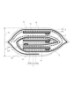
具体的には、図8に示すように、他の実施形態における巻回形の電解コンデンサ51は、主として、コンデンサ素子52と、外装ケース62と、封口体61とから構成される。
[Other embodiments]
(1) In the first embodiment described above, the case where the present invention is applied to the
Specifically, as shown in FIG. 8, a wound
図9および図10に示すように、コンデンサ素子52は、エッチング処理および酸化皮膜形成処理が施された陽極箔55aと陰極箔56aとがセパレータ(電解紙)54を介して所定の巻回方向に巻回され、当該巻回方向(図10において横方向)に巻かれる素子止めテープ59a(第1の素子止めテープ)によって巻き止められている。また、これに加えて、素子止めテープ59aに対して略直交する方向(図10において縦方向)に素子止めテープ59b(第2の素子止めテープ)が巻回されている。この素子止めテープ59bは、陽極箔55aおよび陰極箔56aにそれぞれ接続された一対のリードタブ55b、56bの間を通るように巻回されている。
As shown in FIGS. 9 and 10, the
このコンデンサ素子52は、駆動用電解液が含浸および/または固体電解質が形成された後、有底筒状の外装ケース62(図8)に収納される。
After being impregnated with a driving electrolyte and/or formed with a solid electrolyte, the
外装ケース62の開口部には樹脂やゴムまたは金属等で形成された封口体61が装着され、該開口部は絞り加工またはレーザー溶接により密閉された構造を有する。
A sealing
コンデンサ素子52から引き出されるリードタブ55b、56bにはリード線55c、56cが溶接され、封口体61の外部に引き出されている。外装ケース62は、スリーブ(図示せず)によって被覆される。
Lead
コンデンサ素子52において、陽極箔55aは、アルミニウム、タンタル、ニオブなどの弁作用金属で構成されている。陽極箔55aの表面は、エッチング処理により粗面化されるとともに、陽極酸化(化成)による陽極酸化皮膜が形成されている。
In
また、陰極箔56aも、陽極箔55aと同様にアルミニウムなどで形成され、その表面は粗面化されるとともに自然酸化皮膜が形成されている。
Similarly to the
また、セパレータ54には、有機溶媒を主体とする溶媒と、有機酸塩、無機酸塩からなる溶質と、リン化合物等の添加物を含む電解液が含浸されている。これにより、陽極箔55aと陰極箔56aとの間に液体の電解質層が形成される。さらに、他の電解質として、固体の導電性高分子を陽極箔55aと陰極箔56aとの間に形成したもの、あるいは電解液と固体電解質を併用したものも用いることができる。
なお、セパレータ54には、電気絶縁性を有する絶縁紙が用いられる。
The
Insulating paper having electrical insulation is used for the
陽極箔55aおよび陰極箔56aには、それぞれリードタブ55b、56bが加締めによって接続されている。
Lead
かかる構成の巻回形の電解コンデンサ51においても、第1の実施形態において上述した積層形の電解コンデンサ1の場合と同様にして、電極箔(陽極箔55a、陰極箔56a)の巻回方向である横方向に巻回される素子止めテープ59aとして、PPテープが用いられ、当該素子止めテープ59aに対して直交する方向(縦方向)に巻回される素子止めテープ59bとして、PPSテープが用いられる。
In the wound
このように、巻回形の電解コンデンサ51においても、縦横に異なる性質(伸び率、耐熱性)の素子止めテープ59a、59bを用いることにより、第1の実施形態の場合と同様にして、コンデンサ素子52に素子膨れが発生することを抑制することができる。
As described above, even in the wound type
具体的には、電極箔(陽極箔55a、陰極箔56a)の巻回方向である横方向に用いられる第1の素子止めテープ59aとして、伸び率の高いPPテープを用い、当該素子止めテープ59aに対して略直交する縦方向に用いられる第2の素子止めテープ59bとして、第1の素子止めテープ59aに比べて耐熱性の高いPPSテープを用いることにより、電極箔(陽極箔55a、陰極箔56a)にテンションを掛けながら巻回することができ、これによりコンデンサ素子52の巻回および巻き止めを容易に行うことができるとともに、コンデンサ素子52の厚みD(図10)を薄くすることができる。
Specifically, a PP tape having a high elongation rate is used as the first element-fixing
一方、第2の素子止めテープ59bとして、PPSテープを用いることにより、第1の素子止めテープ59a(PPテープ)に熱収縮が発生し当該熱収縮により接着力の低下が生じる程度の高温となった場合においても、当該第2の素子止めテープ59b(PPSテープ)の熱収縮が抑えられた状態が維持されることにより、コンデンサ素子52の高温下における素子膨れの発生を抑制することができる。
On the other hand, by using a PPS tape as the second element-fixing
(2) 上述の実施形態においては、素子止めテープ6a(59a)としてPPテープを用い、素子止めテープ6b(59b)としてPPSテープを用いる場合について述べたが、これに限られるものではなく、陽極箔2a(55a)および陰極箔3a(56a)の巻回方向(横方向)に用いる第1の素子止めテープ6a、59aよりも耐熱性(高温度環境下での熱収縮が少ない性能)が高い基材からなるテープを、第2の素子止めテープ6b(59b)として、第1の素子止めテープ6a(59a)と併用すればよい。例えば、素子止めテープ6a(59a)としてPPテープを用いるのに対して、素子止めテープ6b(59b)としてPPよりも耐熱性の高いPI(ポリイミド)テープ、PTFE(ポリテトラフルオロエチレン)テープを用いる等、種々のテープの組み合わせを適用することができる。
(2) In the above-described embodiment, the PP tape is used as the
(3) 上述の実施形態においては、横方向および縦方向に伸び率や耐熱性といった性質の異なる異種テープを用いる場合について述べたが、これら異種テープの巻回方向はこれに限られるものではなく、例えば、第1の素子止めテープ6a(59a)および第2の素子止めテープ6b(59b)をいずれも横方向(陽極箔2a(55a)および陰極箔3a(56a)の巻回方向)に巻回するようにしてもよい。また、素子止めテープ6a(59a)に対して素子止めテープ6b(59b)の巻回方向を略直交する方向以外の方向(所定角度により交差する方向)に巻回するようにしてもよい。素子止めテープ6a、6b(59a、59b)を同じ方向に巻回する場合は、巻回された素子止めテープ6a(59a)の上に重ねて素子止めテープ6b(59b)を巻回したり、2つの素子止めテープ6a、6b(59a、59b)を平行にずらして巻回したりするなど、種々の態様で巻回することができる。
(3) In the above-described embodiment, the case of using different types of tapes having different properties such as elongation rate and heat resistance in the horizontal direction and the vertical direction was described, but the winding direction of these different types of tapes is not limited to this. For example, both the first element-fixing
(4) 上述の実施形態においては、第1の素子止めテープ6a(59a)および第2の素子止めテープ6b(59b)を略同一のテープ幅としたが、これに限られるものではなく、必要に応じて種々のテープ幅を適用することができる。例えば、横方向に巻回される素子止めテープ6a(59a)については、陽極箔2a(55a)および陰極箔3a(56a)の幅と同程度までテープ幅を広げ、これに対して縦方向に巻回される素子止めテープ6b、59bについては、陽極タブ2bおよび陰極タブ3bの間(リードタブ55bおよび56bの間)に巻回するためにこれら陽極タブ2bおよび陰極タブ3bの間隔(リードタブ55bおよび56bの間隔)に応じたテープ幅とすればよい。
(4) In the above-described embodiment, the first element-fixing
(5) 上述の実施形態においては、横方向に1本の素子止めテープ6a、59aを用い、縦方向に1本の素子止めテープ6b、59bを用いる場合について述べたが、これらテープの数は種々の数を適用することができる。また、縦方向の素子止めテープ6b、59bの巻回位置は、陽極タブ2bおよび陰極タブ3bの間(リードタブ55bおよび56bの間)を通る位置に限られず、陽極タブ2bおよび陰極タブ3bの外側(リードタブ55bおよび56bの外側)であってもよい。
(5) In the above-described embodiment, the case where one
1、51 電解コンデンサ
2 陽極部
2a、53a 陽極箔
2b 陽極タブ
3 陰極部
3a、53b 陰極箔
3b 陰極タブ
3c 露出部
4、54 セパレータ
6a、6b、59a、59b 素子止めテープ
7 積層体
10、52 コンデンサ素子
21 ケース
22、61 封口体
55b、56b リードタブ
56 リード線
62 外装ケース
1, 51
Claims (3)
前記コンデンサ素子に対して、前記積層体の巻き折り方向または巻回方向に巻回される第1の素子止めテープと、
前記コンデンサ素子に対して、前記積層体の巻き折り方向に略直交する方向または巻回方向に略直交する方向に巻回され、前記第1の素子止めテープと材質が異なる第2の素子止めテープと、を備え、
前記第2の素子止めテープは、前記第1の素子止めテープと比較して耐熱性が高く、前記第1の素子止めテープは、前記第2の素子止めテープと比較して伸び率が高いことを特徴とするコンデンサ。 a capacitor element obtained by folding or winding a laminate in which a cathode foil and an anode foil are laminated with a separator interposed therebetween;
a first element fixing tape wound around the capacitor element in the winding direction or the winding direction of the laminate;
A second element-fixing tape wound around the capacitor element in a direction substantially perpendicular to the winding direction of the laminate or in a direction substantially perpendicular to the winding direction, and made of a material different from that of the first element-fixing tape. and
The second element-fixing tape has higher heat resistance than the first element-fixing tape, and the first element-fixing tape has a higher elongation rate than the second element-fixing tape. A capacitor characterized by
前記外装ケースの開口端を封口するとともに前記コンデンサ素子に接続された前記引き出しリード線が挿通される挿通孔を有する封口体と、
をさらに備え、
前記コンデンサ素子は、
前記積層体として、2枚の帯状の前記セパレータと、前記2枚のセパレータの間に挟まれた帯状の前記陰極箔と、前記2枚のセパレータと前記陰極箔とが巻き折られて形成される隣合う区画の間に前記セパレータに挟まれた状態で配置された短冊状の前記陽極箔とを有し、
前記第1の素子止めテープは前記積層体の巻き折り方向に巻回されることを特徴とする請求項1に記載のコンデンサ。 a bottomed exterior case that houses the capacitor element impregnated with the electrolytic solution;
a sealing body that seals the open end of the exterior case and has an insertion hole through which the lead wire connected to the capacitor element is inserted;
further comprising
The capacitor element is
The laminate is formed by winding and folding two strip-shaped separators, a strip-shaped cathode foil sandwiched between the two separators, and the two separators and the cathode foil. and the strip-shaped anode foil sandwiched between the separators between adjacent sections,
2. The capacitor according to claim 1, wherein said first element-fixing tape is wound in a winding direction of said laminate.
前記外装ケースの開口端を封口するとともに前記コンデンサ素子に接続された前記引き出しリード線が挿通される挿通孔を有する封口体と、
をさらに備え、
前記コンデンサ素子は、前記積層体として、それぞれ帯状の前記セパレータ、前記陰極箔および前記陽極箔が所定の巻回方向に巻回されてなり、
前記第1の素子止めテープは前記積層体の巻回方向に巻回されることを特徴とする請求項1に記載のコンデンサ。 a bottomed exterior case that houses the capacitor element impregnated with the electrolytic solution;
a sealing body that seals the open end of the exterior case and has an insertion hole through which the lead wire connected to the capacitor element is inserted;
further comprising
The capacitor element is formed by winding the strip-shaped separator, the cathode foil, and the anode foil in a predetermined winding direction as the laminated body,
2. The capacitor according to claim 1, wherein said first element fixing tape is wound in the winding direction of said laminate.
Priority Applications (1)
| Application Number | Priority Date | Filing Date | Title |
|---|---|---|---|
| JP2018244261A JP7219084B2 (en) | 2018-12-27 | 2018-12-27 | capacitor |
Applications Claiming Priority (1)
| Application Number | Priority Date | Filing Date | Title |
|---|---|---|---|
| JP2018244261A JP7219084B2 (en) | 2018-12-27 | 2018-12-27 | capacitor |
Publications (2)
| Publication Number | Publication Date |
|---|---|
| JP2020107697A JP2020107697A (en) | 2020-07-09 |
| JP7219084B2 true JP7219084B2 (en) | 2023-02-07 |
Family
ID=71449700
Family Applications (1)
| Application Number | Title | Priority Date | Filing Date |
|---|---|---|---|
| JP2018244261A Active JP7219084B2 (en) | 2018-12-27 | 2018-12-27 | capacitor |
Country Status (1)
| Country | Link |
|---|---|
| JP (1) | JP7219084B2 (en) |
Families Citing this family (1)
| Publication number | Priority date | Publication date | Assignee | Title |
|---|---|---|---|---|
| WO2025178113A1 (en) * | 2024-02-22 | 2025-08-28 | 日本ケミコン株式会社 | Solid electrolytic capacitor and method for manufacturing same |
Citations (6)
| Publication number | Priority date | Publication date | Assignee | Title |
|---|---|---|---|---|
| JP2000188242A (en) | 1998-12-22 | 2000-07-04 | Elna Co Ltd | Capacitor element stopping tape and electrolytic capacitor |
| JP2001093782A (en) | 1999-09-24 | 2001-04-06 | Nippon Chemicon Corp | Electrolytic capacitor |
| JP2001185224A (en) | 1999-12-28 | 2001-07-06 | Japan Storage Battery Co Ltd | Non-aqueous electrolyte secondary battery |
| JP2006093112A (en) | 2004-09-24 | 2006-04-06 | Samsung Sdi Co Ltd | Lithium secondary battery and manufacturing method thereof |
| JP2007103900A (en) | 2005-09-07 | 2007-04-19 | Nippon Chemicon Corp | Capacitor and method of manufacturing same |
| JP2008258222A (en) | 2007-03-31 | 2008-10-23 | Nippon Chemicon Corp | Electrolytic capacitor |
Family Cites Families (2)
| Publication number | Priority date | Publication date | Assignee | Title |
|---|---|---|---|---|
| JPS56110221A (en) * | 1980-02-05 | 1981-09-01 | Nichicon Capacitor Ltd | Electrolytic condenser |
| JPH11283885A (en) * | 1998-03-30 | 1999-10-15 | Nippon Chemicon Corp | Electrolytic capacitor |
-
2018
- 2018-12-27 JP JP2018244261A patent/JP7219084B2/en active Active
Patent Citations (6)
| Publication number | Priority date | Publication date | Assignee | Title |
|---|---|---|---|---|
| JP2000188242A (en) | 1998-12-22 | 2000-07-04 | Elna Co Ltd | Capacitor element stopping tape and electrolytic capacitor |
| JP2001093782A (en) | 1999-09-24 | 2001-04-06 | Nippon Chemicon Corp | Electrolytic capacitor |
| JP2001185224A (en) | 1999-12-28 | 2001-07-06 | Japan Storage Battery Co Ltd | Non-aqueous electrolyte secondary battery |
| JP2006093112A (en) | 2004-09-24 | 2006-04-06 | Samsung Sdi Co Ltd | Lithium secondary battery and manufacturing method thereof |
| JP2007103900A (en) | 2005-09-07 | 2007-04-19 | Nippon Chemicon Corp | Capacitor and method of manufacturing same |
| JP2008258222A (en) | 2007-03-31 | 2008-10-23 | Nippon Chemicon Corp | Electrolytic capacitor |
Also Published As
| Publication number | Publication date |
|---|---|
| JP2020107697A (en) | 2020-07-09 |
Similar Documents
| Publication | Publication Date | Title |
|---|---|---|
| JP5137604B2 (en) | Electrolytic capacitor and manufacturing method thereof | |
| CN103430264B (en) | Ultracapacitor package design | |
| US8218293B2 (en) | Winding-type electrolytic capacitor and method of manufacturing the same | |
| CN101443865B (en) | Aluminum electrolytic capacitor | |
| JP7219084B2 (en) | capacitor | |
| WO2021172440A1 (en) | Electrolytic capacitor and method for producing same | |
| TW201409508A (en) | Solid electrolytic capacitor | |
| TWI624846B (en) | Winding capacitor package structure with non-equal width conductive foil and its wound component | |
| JP2014203885A (en) | Sealing structure of power storage device and electric double layer capacitor | |
| US6839223B2 (en) | Capacitor | |
| JP2021022628A (en) | Capacitor, manufacturing installation of capacitor and manufacturing method of capacitor | |
| JP2013232586A (en) | Electrolytic capacitor and electronic component | |
| JP7219003B2 (en) | Manufacturing method of electrolytic capacitor | |
| JP7495848B2 (en) | Electrolytic capacitor | |
| JP2009026853A (en) | Electric double-layer capacitor | |
| JP6948555B2 (en) | Electrolytic capacitors and their manufacturing methods | |
| JP5560310B2 (en) | Electrolytic capacitor and manufacturing method thereof | |
| JP7410824B2 (en) | Electrolytic capacitor | |
| CN111868862A (en) | Capacitor and method for manufacturing capacitor | |
| JP5822099B2 (en) | Electrolytic capacitor | |
| JP7272859B2 (en) | wound capacitor | |
| WO2018212125A1 (en) | Electrolytic capacitor | |
| JP7272861B2 (en) | Wound energy storage device and manufacturing method thereof | |
| WO2024162158A1 (en) | Electrolytic capacitor and method for manufacturing same | |
| JP5886766B2 (en) | Solid electrolytic capacitor |
Legal Events
| Date | Code | Title | Description |
|---|---|---|---|
| A621 | Written request for application examination |
Free format text: JAPANESE INTERMEDIATE CODE: A621 Effective date: 20210610 |
|
| A977 | Report on retrieval |
Free format text: JAPANESE INTERMEDIATE CODE: A971007 Effective date: 20220721 |
|
| A131 | Notification of reasons for refusal |
Free format text: JAPANESE INTERMEDIATE CODE: A131 Effective date: 20220726 |
|
| A521 | Request for written amendment filed |
Free format text: JAPANESE INTERMEDIATE CODE: A523 Effective date: 20220921 |
|
| TRDD | Decision of grant or rejection written | ||
| A01 | Written decision to grant a patent or to grant a registration (utility model) |
Free format text: JAPANESE INTERMEDIATE CODE: A01 Effective date: 20230117 |
|
| A61 | First payment of annual fees (during grant procedure) |
Free format text: JAPANESE INTERMEDIATE CODE: A61 Effective date: 20230126 |
|
| R150 | Certificate of patent or registration of utility model |
Ref document number: 7219084 Country of ref document: JP Free format text: JAPANESE INTERMEDIATE CODE: R150 |
|
| R250 | Receipt of annual fees |
Free format text: JAPANESE INTERMEDIATE CODE: R250 |