JP7210092B2 - In-situ selective deposition and etching for advanced patterning applications - Google Patents
In-situ selective deposition and etching for advanced patterning applications Download PDFInfo
- Publication number
- JP7210092B2 JP7210092B2 JP2019563215A JP2019563215A JP7210092B2 JP 7210092 B2 JP7210092 B2 JP 7210092B2 JP 2019563215 A JP2019563215 A JP 2019563215A JP 2019563215 A JP2019563215 A JP 2019563215A JP 7210092 B2 JP7210092 B2 JP 7210092B2
- Authority
- JP
- Japan
- Prior art keywords
- substrate
- gas
- metal
- etching
- exposing
- Prior art date
- Legal status (The legal status is an assumption and is not a legal conclusion. Google has not performed a legal analysis and makes no representation as to the accuracy of the status listed.)
- Active
Links
Images


Classifications
-
- H—ELECTRICITY
- H01—ELECTRIC ELEMENTS
- H01L—SEMICONDUCTOR DEVICES NOT COVERED BY CLASS H10
- H01L21/00—Processes or apparatus adapted for the manufacture or treatment of semiconductor or solid state devices or of parts thereof
- H01L21/02—Manufacture or treatment of semiconductor devices or of parts thereof
- H01L21/04—Manufacture or treatment of semiconductor devices or of parts thereof the devices having at least one potential-jump barrier or surface barrier, e.g. PN junction, depletion layer or carrier concentration layer
- H01L21/18—Manufacture or treatment of semiconductor devices or of parts thereof the devices having at least one potential-jump barrier or surface barrier, e.g. PN junction, depletion layer or carrier concentration layer the devices having semiconductor bodies comprising elements of Group IV of the Periodic System or AIIIBV compounds with or without impurities, e.g. doping materials
- H01L21/30—Treatment of semiconductor bodies using processes or apparatus not provided for in groups H01L21/20 - H01L21/26
- H01L21/31—Treatment of semiconductor bodies using processes or apparatus not provided for in groups H01L21/20 - H01L21/26 to form insulating layers thereon, e.g. for masking or by using photolithographic techniques; After treatment of these layers; Selection of materials for these layers
- H01L21/3105—After-treatment
- H01L21/311—Etching the insulating layers by chemical or physical means
- H01L21/31105—Etching inorganic layers
- H01L21/31111—Etching inorganic layers by chemical means
- H01L21/31116—Etching inorganic layers by chemical means by dry-etching
- H01L21/31122—Etching inorganic layers by chemical means by dry-etching of layers not containing Si, e.g. PZT, Al2O3
-
- C—CHEMISTRY; METALLURGY
- C23—COATING METALLIC MATERIAL; COATING MATERIAL WITH METALLIC MATERIAL; CHEMICAL SURFACE TREATMENT; DIFFUSION TREATMENT OF METALLIC MATERIAL; COATING BY VACUUM EVAPORATION, BY SPUTTERING, BY ION IMPLANTATION OR BY CHEMICAL VAPOUR DEPOSITION, IN GENERAL; INHIBITING CORROSION OF METALLIC MATERIAL OR INCRUSTATION IN GENERAL
- C23F—NON-MECHANICAL REMOVAL OF METALLIC MATERIAL FROM SURFACE; INHIBITING CORROSION OF METALLIC MATERIAL OR INCRUSTATION IN GENERAL; MULTI-STEP PROCESSES FOR SURFACE TREATMENT OF METALLIC MATERIAL INVOLVING AT LEAST ONE PROCESS PROVIDED FOR IN CLASS C23 AND AT LEAST ONE PROCESS COVERED BY SUBCLASS C21D OR C22F OR CLASS C25
- C23F1/00—Etching metallic material by chemical means
- C23F1/10—Etching compositions
- C23F1/12—Gaseous compositions
-
- H—ELECTRICITY
- H01—ELECTRIC ELEMENTS
- H01L—SEMICONDUCTOR DEVICES NOT COVERED BY CLASS H10
- H01L21/00—Processes or apparatus adapted for the manufacture or treatment of semiconductor or solid state devices or of parts thereof
- H01L21/02—Manufacture or treatment of semiconductor devices or of parts thereof
- H01L21/02104—Forming layers
- H01L21/02107—Forming insulating materials on a substrate
- H01L21/02109—Forming insulating materials on a substrate characterised by the type of layer, e.g. type of material, porous/non-porous, pre-cursors, mixtures or laminates
- H01L21/02112—Forming insulating materials on a substrate characterised by the type of layer, e.g. type of material, porous/non-porous, pre-cursors, mixtures or laminates characterised by the material of the layer
- H01L21/02172—Forming insulating materials on a substrate characterised by the type of layer, e.g. type of material, porous/non-porous, pre-cursors, mixtures or laminates characterised by the material of the layer the material containing at least one metal element, e.g. metal oxides, metal nitrides, metal oxynitrides or metal carbides
- H01L21/02175—Forming insulating materials on a substrate characterised by the type of layer, e.g. type of material, porous/non-porous, pre-cursors, mixtures or laminates characterised by the material of the layer the material containing at least one metal element, e.g. metal oxides, metal nitrides, metal oxynitrides or metal carbides characterised by the metal
- H01L21/02178—Forming insulating materials on a substrate characterised by the type of layer, e.g. type of material, porous/non-porous, pre-cursors, mixtures or laminates characterised by the material of the layer the material containing at least one metal element, e.g. metal oxides, metal nitrides, metal oxynitrides or metal carbides characterised by the metal the material containing aluminium, e.g. Al2O3
-
- H—ELECTRICITY
- H01—ELECTRIC ELEMENTS
- H01L—SEMICONDUCTOR DEVICES NOT COVERED BY CLASS H10
- H01L21/00—Processes or apparatus adapted for the manufacture or treatment of semiconductor or solid state devices or of parts thereof
- H01L21/02—Manufacture or treatment of semiconductor devices or of parts thereof
- H01L21/02104—Forming layers
- H01L21/02107—Forming insulating materials on a substrate
- H01L21/02109—Forming insulating materials on a substrate characterised by the type of layer, e.g. type of material, porous/non-porous, pre-cursors, mixtures or laminates
- H01L21/02112—Forming insulating materials on a substrate characterised by the type of layer, e.g. type of material, porous/non-porous, pre-cursors, mixtures or laminates characterised by the material of the layer
- H01L21/02172—Forming insulating materials on a substrate characterised by the type of layer, e.g. type of material, porous/non-porous, pre-cursors, mixtures or laminates characterised by the material of the layer the material containing at least one metal element, e.g. metal oxides, metal nitrides, metal oxynitrides or metal carbides
- H01L21/02175—Forming insulating materials on a substrate characterised by the type of layer, e.g. type of material, porous/non-porous, pre-cursors, mixtures or laminates characterised by the material of the layer the material containing at least one metal element, e.g. metal oxides, metal nitrides, metal oxynitrides or metal carbides characterised by the metal
- H01L21/02186—Forming insulating materials on a substrate characterised by the type of layer, e.g. type of material, porous/non-porous, pre-cursors, mixtures or laminates characterised by the material of the layer the material containing at least one metal element, e.g. metal oxides, metal nitrides, metal oxynitrides or metal carbides characterised by the metal the material containing titanium, e.g. TiO2
-
- H—ELECTRICITY
- H01—ELECTRIC ELEMENTS
- H01L—SEMICONDUCTOR DEVICES NOT COVERED BY CLASS H10
- H01L21/00—Processes or apparatus adapted for the manufacture or treatment of semiconductor or solid state devices or of parts thereof
- H01L21/02—Manufacture or treatment of semiconductor devices or of parts thereof
- H01L21/02104—Forming layers
- H01L21/02107—Forming insulating materials on a substrate
- H01L21/02109—Forming insulating materials on a substrate characterised by the type of layer, e.g. type of material, porous/non-porous, pre-cursors, mixtures or laminates
- H01L21/02112—Forming insulating materials on a substrate characterised by the type of layer, e.g. type of material, porous/non-porous, pre-cursors, mixtures or laminates characterised by the material of the layer
- H01L21/02172—Forming insulating materials on a substrate characterised by the type of layer, e.g. type of material, porous/non-porous, pre-cursors, mixtures or laminates characterised by the material of the layer the material containing at least one metal element, e.g. metal oxides, metal nitrides, metal oxynitrides or metal carbides
- H01L21/02175—Forming insulating materials on a substrate characterised by the type of layer, e.g. type of material, porous/non-porous, pre-cursors, mixtures or laminates characterised by the material of the layer the material containing at least one metal element, e.g. metal oxides, metal nitrides, metal oxynitrides or metal carbides characterised by the metal
- H01L21/02194—Forming insulating materials on a substrate characterised by the type of layer, e.g. type of material, porous/non-porous, pre-cursors, mixtures or laminates characterised by the material of the layer the material containing at least one metal element, e.g. metal oxides, metal nitrides, metal oxynitrides or metal carbides characterised by the metal the material containing more than one metal element
-
- H—ELECTRICITY
- H01—ELECTRIC ELEMENTS
- H01L—SEMICONDUCTOR DEVICES NOT COVERED BY CLASS H10
- H01L21/00—Processes or apparatus adapted for the manufacture or treatment of semiconductor or solid state devices or of parts thereof
- H01L21/02—Manufacture or treatment of semiconductor devices or of parts thereof
- H01L21/02104—Forming layers
- H01L21/02107—Forming insulating materials on a substrate
- H01L21/02225—Forming insulating materials on a substrate characterised by the process for the formation of the insulating layer
- H01L21/0226—Forming insulating materials on a substrate characterised by the process for the formation of the insulating layer formation by a deposition process
- H01L21/02263—Forming insulating materials on a substrate characterised by the process for the formation of the insulating layer formation by a deposition process deposition from the gas or vapour phase
- H01L21/02271—Forming insulating materials on a substrate characterised by the process for the formation of the insulating layer formation by a deposition process deposition from the gas or vapour phase deposition by decomposition or reaction of gaseous or vapour phase compounds, i.e. chemical vapour deposition
- H01L21/0228—Forming insulating materials on a substrate characterised by the process for the formation of the insulating layer formation by a deposition process deposition from the gas or vapour phase deposition by decomposition or reaction of gaseous or vapour phase compounds, i.e. chemical vapour deposition deposition by cyclic CVD, e.g. ALD, ALE, pulsed CVD
-
- H—ELECTRICITY
- H01—ELECTRIC ELEMENTS
- H01L—SEMICONDUCTOR DEVICES NOT COVERED BY CLASS H10
- H01L21/00—Processes or apparatus adapted for the manufacture or treatment of semiconductor or solid state devices or of parts thereof
- H01L21/02—Manufacture or treatment of semiconductor devices or of parts thereof
- H01L21/027—Making masks on semiconductor bodies for further photolithographic processing not provided for in group H01L21/18 or H01L21/34
- H01L21/033—Making masks on semiconductor bodies for further photolithographic processing not provided for in group H01L21/18 or H01L21/34 comprising inorganic layers
- H01L21/0334—Making masks on semiconductor bodies for further photolithographic processing not provided for in group H01L21/18 or H01L21/34 comprising inorganic layers characterised by their size, orientation, disposition, behaviour, shape, in horizontal or vertical plane
- H01L21/0337—Making masks on semiconductor bodies for further photolithographic processing not provided for in group H01L21/18 or H01L21/34 comprising inorganic layers characterised by their size, orientation, disposition, behaviour, shape, in horizontal or vertical plane characterised by the process involved to create the mask, e.g. lift-off masks, sidewalls, or to modify the mask, e.g. pre-treatment, post-treatment
-
- H—ELECTRICITY
- H01—ELECTRIC ELEMENTS
- H01L—SEMICONDUCTOR DEVICES NOT COVERED BY CLASS H10
- H01L21/00—Processes or apparatus adapted for the manufacture or treatment of semiconductor or solid state devices or of parts thereof
- H01L21/02—Manufacture or treatment of semiconductor devices or of parts thereof
- H01L21/04—Manufacture or treatment of semiconductor devices or of parts thereof the devices having at least one potential-jump barrier or surface barrier, e.g. PN junction, depletion layer or carrier concentration layer
- H01L21/18—Manufacture or treatment of semiconductor devices or of parts thereof the devices having at least one potential-jump barrier or surface barrier, e.g. PN junction, depletion layer or carrier concentration layer the devices having semiconductor bodies comprising elements of Group IV of the Periodic System or AIIIBV compounds with or without impurities, e.g. doping materials
- H01L21/30—Treatment of semiconductor bodies using processes or apparatus not provided for in groups H01L21/20 - H01L21/26
- H01L21/302—Treatment of semiconductor bodies using processes or apparatus not provided for in groups H01L21/20 - H01L21/26 to change their surface-physical characteristics or shape, e.g. etching, polishing, cutting
- H01L21/306—Chemical or electrical treatment, e.g. electrolytic etching
- H01L21/30604—Chemical etching
-
- H—ELECTRICITY
- H01—ELECTRIC ELEMENTS
- H01L—SEMICONDUCTOR DEVICES NOT COVERED BY CLASS H10
- H01L21/00—Processes or apparatus adapted for the manufacture or treatment of semiconductor or solid state devices or of parts thereof
- H01L21/02—Manufacture or treatment of semiconductor devices or of parts thereof
- H01L21/04—Manufacture or treatment of semiconductor devices or of parts thereof the devices having at least one potential-jump barrier or surface barrier, e.g. PN junction, depletion layer or carrier concentration layer
- H01L21/18—Manufacture or treatment of semiconductor devices or of parts thereof the devices having at least one potential-jump barrier or surface barrier, e.g. PN junction, depletion layer or carrier concentration layer the devices having semiconductor bodies comprising elements of Group IV of the Periodic System or AIIIBV compounds with or without impurities, e.g. doping materials
- H01L21/30—Treatment of semiconductor bodies using processes or apparatus not provided for in groups H01L21/20 - H01L21/26
- H01L21/31—Treatment of semiconductor bodies using processes or apparatus not provided for in groups H01L21/20 - H01L21/26 to form insulating layers thereon, e.g. for masking or by using photolithographic techniques; After treatment of these layers; Selection of materials for these layers
- H01L21/3205—Deposition of non-insulating-, e.g. conductive- or resistive-, layers on insulating layers; After-treatment of these layers
- H01L21/321—After treatment
- H01L21/3213—Physical or chemical etching of the layers, e.g. to produce a patterned layer from a pre-deposited extensive layer
- H01L21/32133—Physical or chemical etching of the layers, e.g. to produce a patterned layer from a pre-deposited extensive layer by chemical means only
- H01L21/32135—Physical or chemical etching of the layers, e.g. to produce a patterned layer from a pre-deposited extensive layer by chemical means only by vapour etching only
-
- H—ELECTRICITY
- H01—ELECTRIC ELEMENTS
- H01L—SEMICONDUCTOR DEVICES NOT COVERED BY CLASS H10
- H01L21/00—Processes or apparatus adapted for the manufacture or treatment of semiconductor or solid state devices or of parts thereof
- H01L21/02—Manufacture or treatment of semiconductor devices or of parts thereof
- H01L21/04—Manufacture or treatment of semiconductor devices or of parts thereof the devices having at least one potential-jump barrier or surface barrier, e.g. PN junction, depletion layer or carrier concentration layer
- H01L21/34—Manufacture or treatment of semiconductor devices or of parts thereof the devices having at least one potential-jump barrier or surface barrier, e.g. PN junction, depletion layer or carrier concentration layer the devices having semiconductor bodies not provided for in groups H01L21/0405, H01L21/0445, H01L21/06, H01L21/16 and H01L21/18 with or without impurities, e.g. doping materials
- H01L21/46—Treatment of semiconductor bodies using processes or apparatus not provided for in groups H01L21/428
- H01L21/461—Treatment of semiconductor bodies using processes or apparatus not provided for in groups H01L21/428 to change their surface-physical characteristics or shape, e.g. etching, polishing, cutting
- H01L21/469—Treatment of semiconductor bodies using processes or apparatus not provided for in groups H01L21/428 to change their surface-physical characteristics or shape, e.g. etching, polishing, cutting to form insulating layers thereon, e.g. for masking or by using photolithographic techniques; After-treatment of these layers
- H01L21/471—Inorganic layers
Description
関連出願の相互参照
本出願は、2017年5月15日に出願された米国仮特許出願第62/506,299号明細書に関するものであり、その優先権を主張し、その全内容が、参照により本願明細書に援用される。本出願は、2017年7月1日に出願された米国仮特許出願第62/528,061号明細書にもまた関するものであり、その優先権を主張し、その全内容が、参照により本願明細書に援用される。
CROSS-REFERENCE TO RELATED APPLICATIONS This application is related to and claims priority from U.S. Provisional Patent Application No. 62/506,299, filed May 15, 2017, the entire contents of which are incorporated by reference. is incorporated herein by This application is also related to, and claims priority from, U.S. Provisional Patent Application No. 62/528,061, filed July 1, 2017, the entire contents of which are incorporated herein by reference. incorporated in the specification.
本発明は、半導体処理及び半導体デバイスに関し、より詳細には、高度なパターン形成用途のためのインサイチュでの選択的堆積及びエッチングに関する。 The present invention relates to semiconductor processing and semiconductor devices, and more particularly to in-situ selective deposition and etching for advanced patterning applications.
より小型のトランジスタが製造されるにつれて、パターン形成されたフィーチャの限界寸法(CD:Critical Dimension)又は解像度により、生産の難易度がますます高くなっている。サブ10nm技術ノードは、設計仕様に対し、厳格な厚さ、均一性、及び原子レベルでほぼマージンや変動がないことが要求される。EUV導入後であってもコスト効率の良いスケーリングが継続できるようにするには、自己整合パターン形成が、オーバーレイ駆動パターン形成(overlay-driven patterning)に取って代わる必要がある。薄膜の選択的エッチング及び堆積は、高度にスケーリングされた技術ノードをパターン形成する際の重要なステップである。 As smaller transistors are manufactured, the critical dimension (CD) or resolution of the patterned features becomes more and more difficult to manufacture. The sub-10 nm technology node requires tight thickness, uniformity, and near-zero margins and variations at the atomic level to design specifications. Self-aligned patterning needs to replace overlay-driven patterning so that cost-effective scaling can continue even after the introduction of EUV. Selective etching and deposition of thin films is a critical step in patterning highly scaled technology nodes.
本発明の実施形態は、高度なパターン形成用途のためのインサイチュでの選択的堆積及びエッチングの方法を提供する。1つの実施形態によれば、方法は、金属含有層を上に有する基板を処理チャンバ内に設けることと、この基板をガスパルスシーケンスに暴露して、プラズマがない状態で金属含有層をエッチングすることであって、このガスパルスシーケンスが、任意の順序で、ハロゲン含有ガスを含んでいる第1の反応ガスに基板を暴露することと、アルキルアルミニウムを含んでいる第2の反応ガスに基板を暴露することと、を含むことと、を含む。 Embodiments of the present invention provide in-situ selective deposition and etching methods for advanced patterning applications. According to one embodiment, a method includes providing a substrate having a metal-containing layer thereon in a processing chamber and exposing the substrate to a gas pulse sequence to etch the metal-containing layer in the absence of a plasma. wherein the gas pulse sequence comprises, in any order, exposing the substrate to a first reactant gas containing a halogen-containing gas and exposing the substrate to a second reactant gas containing an alkylaluminum. including exposing and including.
別の実施形態によれば、方法は、暴露された第1の材料層及び暴露された第2の材料層を有する基板を処理チャンバ内に設けることと、この基板をガスパルスシーケンスに暴露して、追加の材料層を暴露された第1の材料層上に選択的に堆積するが、暴露された第2の材料層上には堆積しないことであって、このガスパルスシーケンスが、任意の順序で、ハロゲン含有ガスを含んでいる第1の反応ガスに基板を暴露することと、アルキルアルミニウムを含んでいる第2の反応ガスに基板を暴露することと、を含むことと、を含む。1つの実施形態によれば、ガスパルスシーケンスに基板を暴露することが、第2の材料層をエッチングする。 According to another embodiment, a method includes providing a substrate having an exposed first material layer and an exposed second material layer in a processing chamber; exposing the substrate to a sequence of gas pulses; , selectively depositing an additional material layer on the exposed first material layer but not on the exposed second material layer, wherein the gas pulse sequence can be in any order. exposing the substrate to a first reactant gas containing a halogen-containing gas; and exposing the substrate to a second reactant gas containing an alkylaluminum. According to one embodiment, exposing the substrate to a gas pulse sequence etches the second material layer.
添付の図面は、この明細書に組み入れられ、この明細書の一部を構成するが、それらは、本発明の実施形態を図示し、上記の本発明の全般的な説明、及び下記の詳細な説明とともに、本発明を説明する役割を果たす。 The accompanying drawings, which are incorporated in and constitute a part of this specification, illustrate embodiments of the present invention and provide a general description of the invention above and a detailed description below. Together with the description, it serves to explain the invention.
本発明の実施形態は、基板上の膜をガスパルスシーケンスに暴露することを含む方法を説明する。1つの実施形態によれば、この方法を使用して金属含有層を熱エッチングすることができる。別の実施形態によれば、この方法を使用して、他の金属含有層に材料を同時に堆積しながら金属含有層を選択的にエッチングすることができる。この方法は、半導体の製造に組み込むことができる。1つの例では、熱エッチング処理をゲートスタック形成及びパターン形成に組み込むことができる。別の例では、デバイスの仕事関数を調整するために、熱エッチング処理を正確な膜厚制御に使用することができる。 Embodiments of the present invention describe methods that include exposing a film on a substrate to a gas pulse sequence. According to one embodiment, the method can be used to thermally etch a metal-containing layer. According to another embodiment, the method can be used to selectively etch metal-containing layers while simultaneously depositing material on other metal-containing layers. The method can be incorporated into semiconductor manufacturing. In one example, a thermal etch process can be incorporated into gate stacking and patterning. In another example, a thermal etch process can be used for precise film thickness control to tune the work function of the device.
本発明のいくつかの実施形態は、金属含有層をエッチングするための等方性の熱原子層エッチング(ALE:Atomic Layer Etching)処理を説明する。金属含有の例には、ハフニウム酸化物(例えば、HfO2)、ハフニウム窒化物(例えば、HfN)などのHf含有化合物、ジルコニウム酸化物(例えば、ZrO2)及びジルコニウム窒化物(例えば、ZrN)などのZr含有化合物、並びに、チタン酸化物(例えば、TiO2)及びチタン窒化物(例えば、TiN)などのTi含有化合物が含まれる。金属酸化物のなかには(例えば、TiO2、HfO2、及びZrO2)、先端半導体デバイス用の有望なhigh-k(ハイカッパ)誘電体材料として識別されているものもある。1つの例では、HfO2がゲート誘電体材料として半導体デバイスで現在使用されている。 Some embodiments of the present invention describe isotropic thermal atomic layer etching (ALE) processes for etching metal-containing layers. Metal-containing examples include Hf-containing compounds such as hafnium oxides ( e.g., HfO2), hafnium nitrides (e.g., HfN), zirconium oxides ( e.g., ZrO2) and zirconium nitrides (e.g., ZrN). and Ti-containing compounds such as titanium oxides (eg, TiO 2 ) and titanium nitrides (eg, TiN). Some metal oxides (eg, TiO 2 , HfO 2 , and ZrO 2 ) have been identified as promising high-k dielectric materials for advanced semiconductor devices. In one example, HfO2 is currently used in semiconductor devices as a gate dielectric material.
1つの実施形態によれば、方法は、金属含有層を上に有する基板を処理チャンバ内に設けることと、この基板をガスパルスシーケンスに暴露して、プラズマがない状態で金属含有層をエッチングすることであって、このガスパルスシーケンスが、任意の順序で、ハロゲン含有ガスを含んでいる第1の反応ガスに基板を暴露することと、アルキルアルミニウムを含んでいる第2の反応ガスに基板を暴露することと、を含むことと、を含む。ガスパルスシーケンスを少なくとも一度繰り返して、金属含有層をさらにエッチングすることができる。1つの実施形態によれば、方法は、第1の反応ガス及び第2の反応ガスに基板を暴露するステップの間で、不活性ガスで処理チャンバをパージすることをさらに含む。 According to one embodiment, a method includes providing a substrate having a metal-containing layer thereon in a processing chamber and exposing the substrate to a gas pulse sequence to etch the metal-containing layer in the absence of a plasma. wherein the gas pulse sequence comprises, in any order, exposing the substrate to a first reactant gas containing a halogen-containing gas and exposing the substrate to a second reactant gas containing an alkylaluminum. including exposing and including. The gas pulse sequence can be repeated at least once to further etch the metal-containing layer. According to one embodiment, the method further includes purging the processing chamber with an inert gas between exposing the substrate to the first reactive gas and the second reactive gas.
1つの実施形態によれば、ハロゲン含有ガスは、TiF4、TiCl4、TiBr4、及びTiI4からなる群から選択されるチタンハロゲン化物を含む。別の実施形態によれば、ハロゲン含有ガスは、SiCl4、BCl3、及びCCl4からなる群から選択することができる。1つの実施形態によれば、アルキルアルミニウムは、トリメチルアルミニウム(AlMe3)、トリエチルアルミニウム(AlEt3)、トリプロピルアルミニウム(AlPr3)、及びトリブチルアルミニウム(AlBu3)からなる群から選択することができる。他の実施形態は、混合配位子を有するアルキルアルミニウム、例えば、AlMe2Et、又はAlMeEt2の使用を含む。いくつかの実施形態によれば、基板の温度は、約200℃~500℃未満、又は約300℃~約400℃とすることができる。ハロゲン含有ガス及びアルキルアルミニウムへの暴露はいずれも、基板表面をハロゲン含有ガス及びアルキルアルミニウムで飽和させる飽和暴露とすることができる。 According to one embodiment, the halogen containing gas comprises a titanium halide selected from the group consisting of TiF4 , TiCl4 , TiBr4 and TiI4 . According to another embodiment, the halogen-containing gas can be selected from the group consisting of SiCl4 , BCl3 , and CCl4 . According to one embodiment, the aluminum alkyl can be selected from the group consisting of trimethylaluminum ( AlMe3 ) , triethylaluminum ( AlEt3 ), tripropylaluminum ( AlPr3 ), and tributylaluminum (AlBu3). . Other embodiments include the use of aluminum alkyls with mixed ligands, such as AlMe2Et , or AlMeEt2 . According to some embodiments, the temperature of the substrate can be from about 200°C to less than 500°C, or from about 300°C to about 400°C. Both exposures to the halogen-containing gas and the aluminum alkyl can be saturation exposures that saturate the substrate surface with the halogen-containing gas and the aluminum alkyl.
図1は、本発明の一実施形態による、基板を処理するためのガスパルスシーケンスを概略的に示す。ガスパルスシーケンスは、プラズマ励起がない状態での順次の反応ガスパルスのサイクルを含む。各サイクルは、ハロゲン含有ガスを含んでいる第1の反応ガスパルス101と、パージガスパルス102(例えば、Ar)と、アルキルアルミニウムを含んでいる第2の反応ガスパルス103と、パージガスパルス104(例えば、Ar)と、を含む。第1の反応ガスパルス101及び第2の反応ガスパルス103は、不活性ガスをさらに含んでいる場合がある。別の実施形態によれば、パージガスパルス102及び104のうちの1つ以上は、省略することができる。
FIG. 1 schematically illustrates a gas pulse sequence for processing a substrate according to one embodiment of the invention. A gas pulse sequence comprises a cycle of sequential reactive gas pulses in the absence of plasma excitation. Each cycle includes a first
基板処理の例
基板上のTiN膜を本発明の一実施形態に従って処理した。TiCl4、Ar、AlMe3、及びArの順次暴露の複数のサイクルを使用して、TiN膜を処理した。TiCl4のパルス長は5秒であり、AlMe3のパルス長は6秒であった。TiCl4パルス及びAlMe3パルスはいずれも、飽和暴露であり、基板の温度は350℃であった。TiN膜の厚さは、0回、50回、150回、及び250回のサイクルの後にX線光電子分光法(XPS:X-ray Photoelectron Spectroscopy)によって測定した。TiN膜のエッチング速度は、約0.1Å/サイクルであった。
Substrate Processing Example A TiN film on a substrate was processed according to one embodiment of the present invention. Multiple cycles of sequential exposures of TiCl 4 , Ar, AlMe 3 , and Ar were used to treat the TiN films. The pulse length of TiCl4 was 5 s and that of AlMe3 was 6 s. Both TiCl 4 and AlMe 3 pulses were saturation exposures and the substrate temperature was 350°C. The thickness of the TiN films was measured by X-ray Photoelectron Spectroscopy (XPS) after 0, 50, 150, and 250 cycles. The etch rate of the TiN film was about 0.1 Å/cycle.
基板上のHfO2膜を本発明の一実施形態に従って処理した。TiCl4、Ar、AlMe3、及びArの順次暴露のサイクルを使用して、HfO2膜を処理した。TiCl4のパルス長は5秒であり、AlMe3のパルス長は6秒であった。TiCl4パルス及びAlMe3パルスはいずれも、飽和暴露であり、基板の温度は350℃であった。HfO2膜の厚さは、0回、20回、50回、及び100回のサイクルの後にXPSによって測定した。HfO2膜のエッチング速度は、約0.37Å/サイクルであった。 A HfO 2 film on a substrate was treated according to one embodiment of the present invention. A cycle of sequential exposures of TiCl 4 , Ar, AlMe 3 , and Ar was used to treat the HfO 2 film. The pulse length of TiCl4 was 5 s and that of AlMe3 was 6 s. Both TiCl 4 and AlMe 3 pulses were saturation exposures and the substrate temperature was 350°C. The thickness of HfO 2 films was measured by XPS after 0, 20, 50 and 100 cycles. The etch rate of the HfO 2 film was about 0.37 Å/cycle.
基板上のZrO2膜を本発明の一実施形態に従って処理した。TiCl4、Ar、AlMe3、及びArの順次暴露のサイクルを使用して、ZrO2膜を処理した。TiCl4のパルス長は5秒であり、AlMe3のパルス長は6秒であった。TiCl4パルス及びAlMe3パルスはいずれも、飽和暴露であり、基板の温度は350℃であった。ZrO2膜の厚さは、0回、20回、50回、及び100回のサイクルの後にXPSによって測定した。ZrO2膜のエッチング速度は、約0.5Å/サイクルであった。 A ZrO2 film on a substrate was treated according to one embodiment of the present invention. A cycle of sequential exposures of TiCl 4 , Ar, AlMe 3 , and Ar was used to treat the ZrO 2 film. The pulse length of TiCl4 was 5 s and that of AlMe3 was 6 s. Both TiCl 4 and AlMe 3 pulses were saturation exposures and the substrate temperature was 350°C. The thickness of ZrO 2 films was measured by XPS after 0, 20, 50 and 100 cycles. The etch rate of the ZrO 2 film was approximately 0.5 Å/cycle.
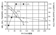
図2は、本発明の実施形態による、基板を処理する実験結果を示す。上述のTiN膜、HfO2膜、及びZrO2膜をエッチングした結果が示されており、基板上のAl2O3膜を処理した実験結果もまた示されている。このAl2O3膜は、図1に示されているTiCl4、Ar、AlMe3、及びArの順次暴露のサイクルを使用して処理した。TiCl4のパルス長は5秒であり、AlMe3のパルス長は6秒であった。基板の温度は350℃であった。図2の実験結果は、HfO2膜、ZrO2膜、及びTiNがガス暴露によってエッチングされ、一方、Al2O3膜はエッチングされなかったことを示し、また、元素分析は、TiAlOX材料がAl2O3膜上に堆積されたことを示した。 FIG. 2 shows experimental results of processing substrates according to embodiments of the present invention. The results of etching the TiN, HfO 2 and ZrO 2 films mentioned above are shown, and the experimental results of processing Al 2 O 3 films on substrates are also shown. The Al 2 O 3 film was processed using the sequential TiCl 4 , Ar, AlMe 3 , and Ar exposure cycles shown in FIG. The pulse length of TiCl4 was 5 s and that of AlMe3 was 6 s. The temperature of the substrate was 350°C. The experimental results in FIG. 2 show that the HfO2 film, ZrO2 film, and TiN were etched by the gas exposure , while the Al2O3 film was not etched, and the elemental analysis also showed that the TiAlO X material was It was shown to be deposited on an Al 2 O 3 film.
1つの実施形態によれば、熱エッチング処理を使用して、ハードマスク堆積及び縦方向の誘電体成長のための領域選択的堆積の際の選択性を維持することができる。1つの実施形態によれば、出発基板が、誘電体材料に象眼された金属含有材料を含んでいる場合がある。金属含有材料の例には、タングステン(W)、ルテニウム(Ru)、コバルト(Co)、及び銅(Cu)などの金属が含まれる。誘電体材料の例には、SiO2、SiON、SiN、SiCN、及びスピンオン酸化物が含まれる場合がある。出発基板は、H2暴露、アニーリング、及びそれらの組み合わせを使用して、前処理することができる。1つの例では、その後、出発基板は、金属含有材料の上に有機化合物の自己組織化単分子層を形成する反応ガスに暴露されて、後続の誘電体材料上への選択的堆積を強化し易くすることができる。その後、少なくとも実質的に選択的に、金属含有層を誘電体材料の上に堆積させることができる。1つの例では、原子層堆積法(ALD:Atomic Layer Deposition)によって金属含有層を堆積させることができる。金属含有材料の核生成サイトで少量の追加の金属含有層を堆積させることができる。追加の金属含有層の量は、金属含有層の量よりも少量であるが、領域選択的堆積の際の選択性を維持するためには、追加の金属含有材料を除去することが必要な場合がある。このため、金属含有材料の上の追加の金属含有層は、ハロゲン含有ガスを含んでいる第1の反応ガス、及びアルキルアルミニウムを含んでいる第2の反応ガスを使用して、上述の熱エッチング処理によって除去することができる。その後、金属含有層の堆積、及び熱エッチングを少なくとも一度繰り返すことができる。 According to one embodiment, a thermal etch process can be used to maintain selectivity during hard mask deposition and area-selective deposition for vertical dielectric growth. According to one embodiment, the starting substrate may include a metal-containing material inlaid with a dielectric material. Examples of metal-containing materials include metals such as tungsten (W), ruthenium (Ru), cobalt (Co), and copper (Cu). Examples of dielectric materials may include SiO2 , SiON, SiN, SiCN, and spin-on oxides. The starting substrate can be pretreated using H2 exposure, annealing, and combinations thereof. In one example, the starting substrate is then exposed to reactive gases that form a self-assembled monolayer of organic compounds on the metal-containing material to enhance selective deposition on subsequent dielectric materials. can be made easier. A metal-containing layer can then be deposited, at least substantially selectively, over the dielectric material. In one example, the metal-containing layer can be deposited by Atomic Layer Deposition (ALD). Small amounts of additional metal-containing layers can be deposited at the nucleation sites of the metal-containing material. The amount of the additional metal-containing layer is less than the amount of the metal-containing layer, but if it is necessary to remove the additional metal-containing material to maintain selectivity during area-selective deposition. There is Thus, the additional metal-containing layer on top of the metal-containing material is thermally etched using a first reactant gas containing a halogen-containing gas and a second reactant gas containing an alkylaluminum, as described above. Can be removed by treatment. Deposition of the metal-containing layer and thermal etching can then be repeated at least once.
1つの実施形態によれば、仕事関数の調整のために熱エッチング処理を使用することができる。半導体デバイスでは、閾値電圧(Vt)を設定することによる仕事関数の調整は、トランジスタの動作にとって重要である。仕事関数を制御するための1つの方法は、ゲートスタックの厚さ全体にわたる。しかしながら、スケーリングされたノードの場合、デバイス上で利用可能な空間は重大な問題であり、また、これは複数のゲート金属を有するスタックを必要とする場合がある。1つの例では、部分的に製造されたデバイスが、high-k層上、又はhigher-k酸化物(SiO2よりもkが高い)上に、初期金属含有層(例えば、TiN)を有する2つのゲート構造を含んでいる。方法は、パターン形成されたマスキング層を形成し、その後、上述の熱エッチング処理を実行することによって、1つのゲート構造から初期金属含有層を除去すること、又は薄層化することを含む。その後、マスキング層を除去し、基板上に追加の金属含有層を堆積し、これにより、追加の金属含有層を有する第1のゲート構造、並びに初期金属含有層及び追加の金属含有層を有する第2のゲート構造を形成することができる。初期金属含有層及び追加の金属含有層は、2つのゲート構造が異なる仕事関数を有するように選択することができる。1つの例では、初期金属含有層及び追加の金属含有層の堆積、並びに熱エッチング処理は、同じ基板温度か、又はほぼ同等の基板温度を使用して、同じ処理チャンバ内で実行することができる。 According to one embodiment, a thermal etching process can be used for work function tuning. In semiconductor devices, tuning the work function by setting the threshold voltage (V t ) is critical to transistor operation. One way to control the workfunction is through the thickness of the gate stack. However, for scaled nodes, available space on the device is a critical issue, and this may require stacks with multiple gate metals. In one example, a partially fabricated device has an initial metal-containing layer (eg, TiN) on a high-k layer, or on a high-k oxide (higher k than SiO) 2 . It contains two gate structures. The method includes removing or thinning the initial metal-containing layer from one gate structure by forming a patterned masking layer and then performing the thermal etching process described above. The masking layer is then removed and an additional metal-containing layer is deposited over the substrate, resulting in a first gate structure having the additional metal-containing layer and a first gate structure having the initial metal-containing layer and the additional metal-containing layer. Two gate structures can be formed. The initial metal-containing layer and the additional metal-containing layers can be selected such that the two gate structures have different work functions. In one example, the deposition of the initial metal-containing layer and the additional metal-containing layer and the thermal etching process can be performed in the same processing chamber using the same or approximately similar substrate temperatures. .
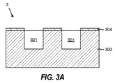
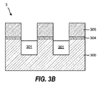
本発明のいくつかの実施形態は、高度なパターン形成用途のためのインサイチュでの選択的堆積及びエッチングの方法を提供する。図3A及び図3Bは、本発明の一実施形態による選択的堆積及びエッチングを概略的に示す。1つの例では、図3Aのパターン形成された基板3は、膜300(例えば、誘電体)内に、第2の材料層301(例えば、TiN)で満たされた凹状フィーチャと、第1の材料層304(例えば、Al2O3)と、を含み、この層は、第1の材料層304上に選択的に形成されているが、第2の材料層301上には形成されない。図3Bは、パターン形成された基板3を、ハロゲン含有ガスを含んでいる第1の反応ガス、及びアルキルアルミニウムを含んでいる第2の反応ガスに交互に暴露することを含むガスパルスシーケンスに暴露した後に得られた構造を示す。ガスパルスへの暴露は、暴露された第1の材料層304上にTiAlOXの層を選択的に堆積するが、暴露された第2の材料層301はエッチングされて、第2の材料層301を凹んだ状態にする。1つの例では、暴露された第1の材料層304は、Al金属、Al2O3、AlN、又はそれらの組み合わせを含んでいる。1つの例では、暴露された第2の材料層304は、TiO2、TiN、HfO2、HfN、ZrO2、ZrN、又はそれらの組み合わせを含んでいる。
Some embodiments of the present invention provide in-situ selective deposition and etching methods for advanced patterning applications. 3A and 3B schematically illustrate selective deposition and etching according to one embodiment of the invention. In one example, the patterned
1つの実施形態によれば、多色パターン形成のための選択的堆積及びエッチングの方法が提供される。多色パターン形成とは、異なる材料の選択的エッチング、及びその後、得られたパターンを使用して、1つ又は複数の下地層をエッチングすることを指す。選択的エッチング及び堆積は、ハロゲン含有ガスを含んでいる第1の反応ガス、及びアルキルアルミニウムを含んでいる第2の反応ガスに交互に暴露することを含むガスパルスシーケンスを使用して行うことができる。 According to one embodiment, a method of selective deposition and etching for multicolor patterning is provided. Multicolor patterning refers to selective etching of different materials and then using the resulting pattern to etch one or more underlying layers. Selective etching and deposition can be performed using a gas pulse sequence that includes alternating exposure to a first reactant gas containing a halogen-containing gas and a second reactant gas containing an alkylaluminum. can.
図4A及び図4Bは、本発明の一実施形態による、多色パターン形成のための選択的堆積及びエッチングの例示的な方法を概略的に示す。図4Aでは、平坦化後のパターン形成された基板4が、左から右に、交互に並んだ材料402、401、402、403、402、405、402を含んでいる。交互に並んだ材料は、ABACADA、又は多色とも呼ばれる場合がある。1つの例では、材料402は、Al2O3を含有し、材料401は、HfO2又はZrO2を含有し、材料403は、TiNを含有し、材料403は、TiO2を含有している。1つの実施形態によれば、基板4は、ハロゲン含有ガスを含んでいる第1の反応ガス、及びアルキルアルミニウムを含んでいる第2の反応ガスに交互に暴露することを含むガスパルスシーケンスに暴露して、材料401(例えば、HfO2)を選択的に除去し、材料403(例えば、TiN)及び材料405(例えば、TiO2)を部分的にエッチングし、そして、材料402(例えば、Al2O3)上に膜406(例えば、TiAlOX)を選択的に堆積することができる。この選択的堆積/エッチング処理は、凹状フィーチャ407、409及び411を形成し、複雑なリソグラフィパターン形成ステップに取って代わることができる。得られた基板4は、材料401(例えば、HfO2)が選択的に除去されている新たなパターンに従って、下地層(すなわち、その基層400)をエッチングすることによってさらに処理することができる。
Figures 4A and 4B schematically illustrate an exemplary method of selective deposition and etching for multicolor patterning, according to one embodiment of the present invention. In FIG. 4A, the patterned
高度なパターン形成用途のためのインサイチュでの選択的堆積及び熱エッチングの複数の実施形態について説明してきた。本発明の実施形態の上述の説明は、例示及び説明を目的として提示したものである。この説明は、網羅的であること、又は開示されている厳密な形態に本発明を限定することを意図するものではない。本明細書及び以下の特許請求の範囲は、説明目的でのみ使用される用語を含み、限定するものとして解釈されないものとする。関連する技術分野の当業者であれば、上記教示に照らして多くの修正及び変形が可能であることを理解することができる。当業者は、図に示されている様々な構成要素の様々な等価な組み合わせ及び置換を認識するであろう。したがって、本発明の範囲は、この詳細な説明によってではなく、むしろ本明細書に添付の特許請求の範囲によって限定されることを意図している。 Several embodiments of in-situ selective deposition and thermal etching for advanced patterning applications have been described. The foregoing descriptions of embodiments of the invention have been presented for purposes of illustration and description. This description is not intended to be exhaustive or to limit the invention to the precise forms disclosed. It is intended that this specification and the claims that follow include terms that are used for descriptive purposes only and are not to be construed as limiting. Persons skilled in the relevant art can appreciate that many modifications and variations are possible in light of the above teachings. Those skilled in the art will recognize various equivalent combinations and permutations of the various components shown in the figures. It is therefore intended that the scope of the invention be limited not by this detailed description, but rather by the claims appended hereto.
Claims (4)
金属含有層を上に有する基板を処理チャンバ内に設けることと、
前記基板をガスパルスシーケンスに暴露して、プラズマがない状態で前記金属含有層をエッチングすることであって、前記ガスパルスシーケンスが、任意の順序で、
ハロゲン含有ガスを含んでいる第1の反応ガスに前記基板を暴露することとであって、前記ハロゲン含有ガスが、TiF4、TiCl4、TiBr4、及びTiI4からなる群から選択されるチタンハロゲン化物を含み、
アルキルアルミニウムを含んでいる第2の反応ガスに前記基板を暴露することと、
を含むことと、を含む方法。 A method of processing a substrate, comprising:
providing a substrate having a metal-containing layer thereon in a processing chamber;
exposing the substrate to a gas pulse sequence to etch the metal-containing layer in the absence of a plasma, the gas pulse sequence comprising, in any order,
exposing the substrate to a first reactant gas comprising a halogen-containing gas, wherein the halogen-containing gas is titanium selected from the group consisting of TiF4 , TiCl4 , TiBr4 , and TiI4 . containing halides,
exposing the substrate to a second reactive gas comprising an alkylaluminum;
including and a method of including.
Priority Applications (1)
| Application Number | Priority Date | Filing Date | Title |
|---|---|---|---|
| JP2022126823A JP7459420B2 (en) | 2017-05-15 | 2022-08-09 | In-situ selective deposition and etching for advanced patterning applications |
Applications Claiming Priority (5)
| Application Number | Priority Date | Filing Date | Title |
|---|---|---|---|
| US201762506299P | 2017-05-15 | 2017-05-15 | |
| US62/506,299 | 2017-05-15 | ||
| US201762528061P | 2017-07-01 | 2017-07-01 | |
| US62/528,061 | 2017-07-01 | ||
| PCT/US2018/032743 WO2018213295A1 (en) | 2017-05-15 | 2018-05-15 | In-situ selective deposition and etching for advanced patterning applications |
Related Child Applications (1)
| Application Number | Title | Priority Date | Filing Date |
|---|---|---|---|
| JP2022126823A Division JP7459420B2 (en) | 2017-05-15 | 2022-08-09 | In-situ selective deposition and etching for advanced patterning applications |
Publications (3)
| Publication Number | Publication Date |
|---|---|
| JP2020520125A JP2020520125A (en) | 2020-07-02 |
| JP2020520125A5 JP2020520125A5 (en) | 2021-04-15 |
| JP7210092B2 true JP7210092B2 (en) | 2023-01-23 |
Family
ID=64097990
Family Applications (2)
| Application Number | Title | Priority Date | Filing Date |
|---|---|---|---|
| JP2019563215A Active JP7210092B2 (en) | 2017-05-15 | 2018-05-15 | In-situ selective deposition and etching for advanced patterning applications |
| JP2022126823A Active JP7459420B2 (en) | 2017-05-15 | 2022-08-09 | In-situ selective deposition and etching for advanced patterning applications |
Family Applications After (1)
| Application Number | Title | Priority Date | Filing Date |
|---|---|---|---|
| JP2022126823A Active JP7459420B2 (en) | 2017-05-15 | 2022-08-09 | In-situ selective deposition and etching for advanced patterning applications |
Country Status (5)
| Country | Link |
|---|---|
| US (1) | US10529584B2 (en) |
| JP (2) | JP7210092B2 (en) |
| KR (3) | KR20230019219A (en) |
| TW (1) | TWI801385B (en) |
| WO (1) | WO2018213295A1 (en) |
Families Citing this family (3)
| Publication number | Priority date | Publication date | Assignee | Title |
|---|---|---|---|---|
| EP3503164A1 (en) * | 2017-12-21 | 2019-06-26 | IMEC vzw | Selective deposition of metal-organic frameworks |
| EP3919979A1 (en) | 2020-06-02 | 2021-12-08 | Imec VZW | Resistless patterning mask |
| KR20240006268A (en) | 2022-07-06 | 2024-01-15 | 에스케이스페셜티 주식회사 | Atomic layer etching method of metal oxide layer |
Citations (2)
| Publication number | Priority date | Publication date | Assignee | Title |
|---|---|---|---|---|
| WO2016100873A1 (en) | 2014-12-18 | 2016-06-23 | The Regents Of The University Of Colorado, A Body Corporate | Novel methods of atomic layer etching (ale) using sequential, self-limiting thermal reactions |
| US20180182597A1 (en) | 2016-12-22 | 2018-06-28 | Asm Ip Holding B.V. | Atomic layer etching processes |
Family Cites Families (20)
| Publication number | Priority date | Publication date | Assignee | Title |
|---|---|---|---|---|
| US4902645A (en) | 1987-08-24 | 1990-02-20 | Fujitsu Limited | Method of selectively forming a silicon-containing metal layer |
| KR920003555B1 (en) * | 1989-11-13 | 1992-05-04 | 이시영 | Filter for water purifier |
| JP3334911B2 (en) * | 1992-07-31 | 2002-10-15 | キヤノン株式会社 | Pattern formation method |
| JPH0758712B2 (en) * | 1993-02-18 | 1995-06-21 | 日本電気株式会社 | Wiring formation method |
| JPH06275529A (en) * | 1993-03-22 | 1994-09-30 | Hitachi Ltd | Manufacturing method of compound semiconductor device |
| US7157385B2 (en) * | 2003-09-05 | 2007-01-02 | Micron Technology, Inc. | Method of depositing a silicon dioxide-comprising layer in the fabrication of integrated circuitry |
| US20040198069A1 (en) * | 2003-04-04 | 2004-10-07 | Applied Materials, Inc. | Method for hafnium nitride deposition |
| US20060165994A1 (en) * | 2004-07-07 | 2006-07-27 | General Electric Company | Protective coating on a substrate and method of making thereof |
| JP5719138B2 (en) * | 2009-12-22 | 2015-05-13 | 株式会社日立国際電気 | Semiconductor device manufacturing method and substrate processing method |
| US8293658B2 (en) * | 2010-02-17 | 2012-10-23 | Asm America, Inc. | Reactive site deactivation against vapor deposition |
| US20140051256A1 (en) | 2012-08-15 | 2014-02-20 | Lam Research Corporation | Etch with mixed mode pulsing |
| CN103681269B (en) * | 2012-09-03 | 2016-06-29 | 中芯国际集成电路制造(上海)有限公司 | The method of selectively formed high-K dielectric layer |
| US8841182B1 (en) * | 2013-03-14 | 2014-09-23 | Asm Ip Holding B.V. | Silane and borane treatments for titanium carbide films |
| TW201525173A (en) * | 2013-12-09 | 2015-07-01 | Applied Materials Inc | Methods of selective layer deposition |
| US9583401B2 (en) | 2014-02-12 | 2017-02-28 | International Business Machines Corporation | Nano deposition and ablation for the repair and fabrication of integrated circuits |
| JP6243290B2 (en) | 2014-05-01 | 2017-12-06 | 東京エレクトロン株式会社 | Film forming method and film forming apparatus |
| WO2016210299A1 (en) * | 2015-06-26 | 2016-12-29 | Tokyo Electron Limited | GAS PHASE ETCH WITH CONTROLLABLE ETCH SELECTIVITY OF Si-CONTAINING ARC OR SILICON OXYNITRIDE TO DIFFERENT FILMS OR MASKS |
| US10566185B2 (en) | 2015-08-05 | 2020-02-18 | Asm Ip Holding B.V. | Selective deposition of aluminum and nitrogen containing material |
| US20170243755A1 (en) * | 2016-02-23 | 2017-08-24 | Tokyo Electron Limited | Method and system for atomic layer etching |
| US10453737B2 (en) * | 2017-04-11 | 2019-10-22 | Tokyo Electron Limited | Method of filling retrograde recessed features with no voids |
-
2018
- 2018-05-15 TW TW107116408A patent/TWI801385B/en active
- 2018-05-15 KR KR1020237002883A patent/KR20230019219A/en not_active Application Discontinuation
- 2018-05-15 US US15/980,274 patent/US10529584B2/en active Active
- 2018-05-15 WO PCT/US2018/032743 patent/WO2018213295A1/en active Application Filing
- 2018-05-15 JP JP2019563215A patent/JP7210092B2/en active Active
- 2018-05-15 KR KR1020197035798A patent/KR102553117B1/en active IP Right Grant
- 2018-05-15 KR KR1020237024417A patent/KR102631150B1/en active IP Right Grant
-
2022
- 2022-08-09 JP JP2022126823A patent/JP7459420B2/en active Active
Patent Citations (2)
| Publication number | Priority date | Publication date | Assignee | Title |
|---|---|---|---|---|
| WO2016100873A1 (en) | 2014-12-18 | 2016-06-23 | The Regents Of The University Of Colorado, A Body Corporate | Novel methods of atomic layer etching (ale) using sequential, self-limiting thermal reactions |
| US20180182597A1 (en) | 2016-12-22 | 2018-06-28 | Asm Ip Holding B.V. | Atomic layer etching processes |
Also Published As
| Publication number | Publication date |
|---|---|
| KR20230110664A (en) | 2023-07-24 |
| WO2018213295A1 (en) | 2018-11-22 |
| KR20190142407A (en) | 2019-12-26 |
| JP7459420B2 (en) | 2024-04-02 |
| JP2022145838A (en) | 2022-10-04 |
| US20180330963A1 (en) | 2018-11-15 |
| TWI801385B (en) | 2023-05-11 |
| KR102553117B1 (en) | 2023-07-06 |
| KR102631150B1 (en) | 2024-01-29 |
| JP2020520125A (en) | 2020-07-02 |
| US10529584B2 (en) | 2020-01-07 |
| KR20230019219A (en) | 2023-02-07 |
| TW201907444A (en) | 2019-02-16 |
Similar Documents
| Publication | Publication Date | Title |
|---|---|---|
| JP7459420B2 (en) | In-situ selective deposition and etching for advanced patterning applications | |
| JP4055941B2 (en) | Method for depositing high dielectric constant materials on a substrate using atomic layer deposition | |
| JP6306661B2 (en) | Method for forming an ALD suppression layer using a self-assembled monolayer | |
| TWI698544B (en) | Method for selectively depositing material and method for selectively depositing metal oxide film | |
| JP7330664B2 (en) | Selective metal oxide deposition using self-assembled monolayer surface pretreatment | |
| JP2023015253A (en) | Semiconductor processing apparatus | |
| US20200199751A1 (en) | Deposition tool and method for depositing metal oxide films on organic materials | |
| JP2017208534A (en) | Method for forming film bottom-up in recessed feature | |
| JP2021044364A (en) | Formation method of etching mask and manufacturing method of semiconductor device | |
| JP7348964B2 (en) | Metal oxide etching using fluorine and metal halides | |
| US10199223B2 (en) | Semiconductor device fabrication using etch stop layer | |
| JP3756456B2 (en) | Manufacturing method of semiconductor device | |
| JP2023513110A (en) | How to use an ultra-thin etch stop layer in selective atomic layer etching | |
| KR20200137016A (en) | Area selective deposition for improved contact cap layer formation | |
| KR102553120B1 (en) | Method of filling retrograde recessed features | |
| TW202301437A (en) | Atomic layer deposition of aluminum oxide films for semiconductor devices using an aluminum alkoxide oxidizer | |
| US20180294168A1 (en) | Method for anisotropic dry etching of titanium-containing films | |
| TW202407131A (en) | Methods of selective deposition of molybdenum | |
| KR20040042258A (en) | Method of forming thin film for semiconductor device using atomic layer deposition |
Legal Events
| Date | Code | Title | Description |
|---|---|---|---|
| A521 | Request for written amendment filed |
Free format text: JAPANESE INTERMEDIATE CODE: A523 Effective date: 20210303 |
|
| A621 | Written request for application examination |
Free format text: JAPANESE INTERMEDIATE CODE: A621 Effective date: 20210303 |
|
| A131 | Notification of reasons for refusal |
Free format text: JAPANESE INTERMEDIATE CODE: A131 Effective date: 20220510 |
|
| A521 | Request for written amendment filed |
Free format text: JAPANESE INTERMEDIATE CODE: A523 Effective date: 20220809 |
|
| TRDD | Decision of grant or rejection written | ||
| A01 | Written decision to grant a patent or to grant a registration (utility model) |
Free format text: JAPANESE INTERMEDIATE CODE: A01 Effective date: 20221213 |
|
| A711 | Notification of change in applicant |
Free format text: JAPANESE INTERMEDIATE CODE: A711 Effective date: 20230106 |
|
| A61 | First payment of annual fees (during grant procedure) |
Free format text: JAPANESE INTERMEDIATE CODE: A61 Effective date: 20230106 |
|
| R150 | Certificate of patent or registration of utility model |
Ref document number: 7210092 Country of ref document: JP Free format text: JAPANESE INTERMEDIATE CODE: R150 |