JP7207903B2 - Light source device and projection display device having the same - Google Patents

Light source device and projection display device having the same Download PDF

Info

Publication number
JP7207903B2
JP7207903B2 JP2018157277A JP2018157277A JP7207903B2 JP 7207903 B2 JP7207903 B2 JP 7207903B2 JP 2018157277 A JP2018157277 A JP 2018157277A JP 2018157277 A JP2018157277 A JP 2018157277A JP 7207903 B2 JP7207903 B2 JP 7207903B2
Authority
JP
Japan
Prior art keywords
phosphor
light
light source
heat
source device
Prior art date
Legal status (The legal status is an assumption and is not a legal conclusion. Google has not performed a legal analysis and makes no representation as to the accuracy of the status listed.)
Active
Application number
JP2018157277A
Other languages
Japanese (ja)
Other versions
JP2019095771A (en
JP2019095771A5 (en
Inventor
明広 大谷
雅之 阿部
稔 大古場
Current Assignee (The listed assignees may be inaccurate. Google has not performed a legal analysis and makes no representation or warranty as to the accuracy of the list.)
Canon Inc
Original Assignee
Canon Inc
Priority date (The priority date is an assumption and is not a legal conclusion. Google has not performed a legal analysis and makes no representation as to the accuracy of the date listed.)
Filing date
Publication date
Application filed by Canon Inc filed Critical Canon Inc
Priority to US16/192,519 priority Critical patent/US10567717B2/en
Publication of JP2019095771A publication Critical patent/JP2019095771A/en
Publication of JP2019095771A5 publication Critical patent/JP2019095771A5/ja
Application granted granted Critical
Publication of JP7207903B2 publication Critical patent/JP7207903B2/en
Active legal-status Critical Current
Anticipated expiration legal-status Critical

Links

Images

Description

本発明は光源装置、およびこれを有する投射型表示装置に関し、特に固体光源を有する光源装置に関する。 The present invention relates to a light source device and a projection display device having the same, and more particularly to a light source device having a solid-state light source.

近年、プロジェクタ(投写型表示装置)の光源として、高耐久かつ高輝度の要求から、レーザーダイオード等の半導体発光素子を用いたレーザー光源(固体光源)が注目されている。 2. Description of the Related Art In recent years, a laser light source (solid-state light source) using a semiconductor light-emitting element such as a laser diode has attracted attention as a light source for a projector (projection display device) because of the demand for high durability and high brightness.

レーザー光源として青色光を照射するレーザーダイオード等を用いる場合、射出された青色光を、集光光学系を介して蛍光体上に集光させ、波長を変換し(蛍光変換)、緑色光と赤色光を含む光を射出する構成のプロジェクタが知られている。 When using a laser diode or the like that emits blue light as a laser light source, the emitted blue light is condensed on a phosphor via a condensing optical system, and the wavelength is converted (fluorescence conversion) to produce green light and red light. A projector configured to emit light including light is known.

このようにレーザー光を蛍光体に集光させると、微小な領域にエネルギーが集中するので、蛍光体の温度が上昇してしまう。蛍光体が高温になると、蛍光変換の効率が低下したり、蛍光体が変性して光源としての寿命が損なわれたりする課題があった。 When the laser light is focused on the phosphor in this way, the energy is concentrated in a minute area, so the temperature of the phosphor rises. When the temperature of the phosphor reaches a high temperature, there is a problem that the efficiency of fluorescence conversion decreases, or the phosphor denatures, shortening its life as a light source.

特許文献1に開示された光源装置は、蛍光体の一面を熱抵抗の低い基板に密着させることにより、蛍光体の熱を基板からヒートシンクに伝熱させている。同時に、蛍光体のその他の一面を集光光学系に密着させることにより、蛍光体の熱を集光光学系から周囲のスペーサーに伝熱させ冷却効率を高めている。これに加えて、スペーサーは蛍光体の周囲を密閉するように構成されており、光エネルギーによる蛍光体への塵埃や微粒子等の付着を抑制でき、光源装置をより高寿命化することができる。 In the light source device disclosed in Patent Document 1, the heat of the phosphor is transferred from the substrate to the heat sink by bringing one surface of the phosphor into close contact with the substrate with low thermal resistance. At the same time, by bringing the other surface of the phosphor into close contact with the condensing optical system, the heat of the phosphor is transferred from the condensing optical system to the surrounding spacers, thereby enhancing the cooling efficiency. In addition, the spacer is configured to hermetically seal the periphery of the phosphor, thereby suppressing the adhesion of dust, fine particles, etc. to the phosphor due to light energy, thereby extending the life of the light source device.

特開2014-165058号公報JP 2014-165058 A

上述のように特許文献1では、蛍光体の面を集光光学系に密着させて、蛍光体の熱を集光光学系に伝わるようにしているが、集光光学系の材質としては、ガラスや石英が使われているため十分な放熱ができない場合も考えられる。 As described above, in Patent Document 1, the surface of the phosphor is brought into close contact with the condensing optical system so that the heat of the phosphor is transferred to the condensing optical system. or quartz is used, it may not be possible to dissipate heat sufficiently.

そこで本発明の目的は、蛍光体の冷却効率を向上できる光源装置、およびこれを有する投射型表示装置を提供することである。 SUMMARY OF THE INVENTION Accordingly, an object of the present invention is to provide a light source device capable of improving the cooling efficiency of phosphors, and a projection display device having the same.

上記の目的を達成するために、本発明の一側面としての光源装置は、光源からの光の波長を変換する蛍光体を備える波長変換素子と、該波長変換素子に前記光源からの光を集光させる集光部材と、前記集光部材よりも熱伝導率が大きい熱伝導部材を有し、前記集光部材は、前記熱伝導部材を介さずに前記波長変換素子と対向する透過部と、前記波長変換素子に対する間隔が前記透過部よりも広い凹部を含み、前記蛍光体と前記熱伝導部材前記凹部とは、前記集光部材の光軸方向から見たときに少なくとも一部がこの順に重なって配置され、前記蛍光体と前記熱伝導部材の少なくとも一部が接触していることを特徴とする。 In order to achieve the above object, a light source device as one aspect of the present invention includes a wavelength conversion element provided with a phosphor that converts the wavelength of light from a light source, and concentrating the light from the light source on the wavelength conversion element. a light-condensing member that emits light; and a heat-conducting member having a thermal conductivity higher than that of the light-collecting member, wherein the light-collecting member faces the wavelength conversion element without the heat-conducting member interposed therebetween; At least a portion of the phosphor, the heat-conducting member , and the recess are arranged in this order when viewed from the optical axis direction of the light-condensing member. At least a part of the phosphor and the heat-conducting member are in contact with each other.

本発明によれば、蛍光体の冷却効率を向上できる光源装置、およびこれを有する投射型表示装置を提供することができる。 ADVANTAGE OF THE INVENTION According to this invention, the light source device which can improve the cooling efficiency of fluorescent substance, and a projection-type display apparatus which has the same can be provided.

実施例1に係る投射型表示装置の光学配置図FIG. 1 is an optical layout diagram of a projection display device according to the first embodiment; 実施例1に係る蛍光体の周囲の構成の断面図FIG. 2 is a cross-sectional view of the configuration around the phosphor according to Example 1; 実施例1に係る蛍光体の周囲の構成をレーザー光が入射する向きから見た図FIG. 2 is a view of the configuration around the phosphor according to Example 1, viewed from the direction of incidence of laser light; 実施例1に係る蛍光体の周囲の構成の変形例の模式図Schematic diagram of a modification of the configuration around the phosphor according to Example 1 実施例2に係る蛍光体の周囲の構成の断面図Sectional view of the configuration around the phosphor according to Example 2 実施例2に係る蛍光体の周囲の構成をレーザー光が入射する向きから見た図The figure which looked at the structure around the fluorescent substance which concerns on Example 2 from the direction in which a laser beam injects.

以下に、本発明の好ましい実施の形態を、添付の図面に基づいて詳細に説明する。 Preferred embodiments of the present invention are described in detail below with reference to the accompanying drawings.

(実施例1)
(光学的構成)
はじめに、図1を参照しながら本発明の実施例1に係る光源装置20、およびこれを有する投射型表示装置10の光学的構成について説明する。
(Example 1)
(optical configuration)
First, referring to FIG. 1, the optical configuration of a light source device 20 and a projection display device 10 having the light source device 20 according to Example 1 of the present invention will be described.

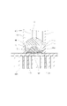
図1は、実施例1に係る投射型表示装置10の光学配置図である。 FIG. 1 is an optical layout diagram of a projection display device 10 according to the first embodiment.

(光源装置)
光源装置20は、複数のLD(個体光源)31、圧縮光学系、集光光学系、蛍光体51などから構成される。本実施例では、LD31は青色のレーザー光100を射出するレーザーダイオード(半導体レーザー)である。
(light source device)
The light source device 20 includes a plurality of LDs (solid light sources) 31, a compression optical system, a condensing optical system, a phosphor 51, and the like. In this embodiment, the LD 31 is a laser diode (semiconductor laser) that emits blue laser light 100 .

圧縮光学系は、コリメータレンズ32、反射ミラーアレイ33、折り返しミラー36、メニスカスレンズ35を有する。圧縮光学系は、LD31からのレーザー光(励起光)100(図1中の破線で示す)の光束の大きさを圧縮して小さくし、後述の集光光学系に向けて出射する。 The compression optical system has a collimator lens 32 , a reflecting mirror array 33 , a folding mirror 36 and a meniscus lens 35 . The compression optical system compresses and reduces the size of the laser light (excitation light) 100 (indicated by the dashed line in FIG. 1) from the LD 31, and emits it toward the later-described condensing optical system.

集光光学系は、第1のマイクロレンズアレイ41、第2のマイクロレンズアレイ42、ダイクロイックミラー43、第1のコンデンサレンズ44、第2のコンデンサレンズ45、を有する。圧縮光学系から出射されたレーザー光100は、集光光学系によって後述する波長変換素子の一部を構成する蛍光体51上に、特定のスポット径となるように集光され、照射される。 The condensing optical system has a first microlens array 41 , a second microlens array 42 , a dichroic mirror 43 , a first condenser lens 44 and a second condenser lens 45 . The laser beam 100 emitted from the compression optical system is condensed by the condensing optical system so as to have a specific spot diameter on the phosphor 51 constituting part of the wavelength conversion element described later, and irradiated.

蛍光体51は、レーザー光100の一部を波長変換し、赤のスペクトルと緑のスペクトルとを主波長域とする光にする(蛍光変換する)。具体的には、蛍光体51は励起光として照射されると、励起光の波長を変換して励起光とは異なる波長の蛍光を生じさせる特性を持つ蛍光材料を低融点ガラスに分散して基材に固着させて設けることができる。なお低融点ガラスは、そのガラス転移温度が通常のガラスよりも低い(例えば600度以下)ガラスである。 The phosphor 51 wavelength-converts a portion of the laser light 100 into light having main wavelength regions of the red spectrum and the green spectrum (performs fluorescence conversion). Specifically, when the phosphor 51 is irradiated as excitation light, a fluorescent material having a property of converting the wavelength of the excitation light to generate fluorescence with a wavelength different from that of the excitation light is dispersed in a low-melting glass. It can be fixed to the material. Low-melting-point glass is glass whose glass transition temperature is lower than that of ordinary glass (for example, 600° C. or less).

蛍光体51で波長変換された光は、波長変換素子の一部を構成する高反射層52によって反射され波長変換素子から出射されることになる。また、レーザー光100の一部は、波長変換素子に照射されても蛍光体51によって波長変換されず、青色光のまま高反射層52によって反射され蛍光体51から射出される。 The light wavelength-converted by the phosphor 51 is reflected by the highly reflective layer 52 forming part of the wavelength conversion element and emitted from the wavelength conversion element. Further, part of the laser light 100 is not wavelength-converted by the phosphor 51 even when the wavelength conversion element is irradiated, and is reflected by the high reflection layer 52 as blue light and emitted from the phosphor 51 .

つまり、高反射層52で反射され波長変換素子から出射される光は赤、緑、青の3原色の光であり、白色光101(図1中の実線で示す)として出射される。白色光101は、再び第1のコンデンサレンズ44、第2のコンデンサレンズ45、ダイクロイックミラー43に向かう。 That is, the light reflected by the highly reflective layer 52 and emitted from the wavelength conversion element is light of the three primary colors of red, green, and blue, and is emitted as white light 101 (indicated by solid lines in FIG. 1). White light 101 is directed to first condenser lens 44 , second condenser lens 45 and dichroic mirror 43 again.

ダイクロイックミラー43の表面には多層膜がコーティングされている。この多層膜は、入射光の波長によって入射光を反射したり透過させたりする特性を有する。すなわち多層膜は波長選択性を有する反射膜であり、青色光は反射し、蛍光体により波長変換された赤色光と緑色光は透過する特性を有する。 The surface of the dichroic mirror 43 is coated with a multilayer film. This multilayer film has the property of reflecting or transmitting incident light depending on the wavelength of the incident light. That is, the multilayer film is a reflective film having wavelength selectivity, and has the characteristic of reflecting blue light and transmitting red light and green light wavelength-converted by the phosphor.

したがって、赤色、緑色の光はダイクロイックミラー43を通過できる。青色の光は、ダイクロイックミラー43に一部が反射されるが、ダイクロイックミラー43の外側を通過できる。したがって、光源装置20から取り出せる光は赤、緑、青の3原色の光、すなわち白色光101である。 Therefore, red and green light can pass through the dichroic mirror 43 . Blue light is partially reflected by the dichroic mirror 43 but can pass outside the dichroic mirror 43 . Therefore, the light that can be extracted from the light source device 20 is the three primary colors of red, green, and blue, that is, white light 101 .

そして、光源装置20から射出された白色光101はアフォーカルレンズ47によって光束を拡大され、後述する照明光学系へ向かう。 The white light 101 emitted from the light source device 20 is expanded by the afocal lens 47 and directed to an illumination optical system, which will be described later.

なお、本実施例では光源装置20の光学的構成の一例として上記の構成を説明した。しかし、光源装置の構成はこれと異なってもよい。すなわち光源装置としては、光源からの光を蛍光体に集光する集光光学系と、集光された光の少なくとも一部の光を、入光した光の波長とは異なる波長に変換する蛍光体を有していればよく、目的に応じてその他の光学系を構成してもよい。 In this embodiment, the above configuration has been described as an example of the optical configuration of the light source device 20 . However, the configuration of the light source device may differ from this. That is, the light source device includes a condensing optical system for condensing the light from the light source onto the phosphor, and a fluorescent light system for converting at least part of the condensed light into a wavelength different from the wavelength of the incident light. It is sufficient that it has a body, and other optical systems may be configured according to the purpose.

(照明光学系)
照明光学系は、第1のフライアイレンズ61、第2のフライアイレンズ62、偏光変換素子63、第1のコンデンサレンズ64、第2のコンデンサレンズ65、第三のコンデンサレンズ66を備える。白色光101は第1のフライアイレンズ61および第2のフライアイレンズ62を透過する事により明るさが均一化され、さらに色も重畳するため色ムラの少ない光束を得ることができる。
(illumination optical system)
The illumination optical system includes a first fly-eye lens 61 , a second fly-eye lens 62 , a polarization conversion element 63 , a first condenser lens 64 , a second condenser lens 65 and a third condenser lens 66 . The white light 101 passes through the first fly-eye lens 61 and the second fly-eye lens 62 so that the brightness is made uniform, and colors are also superimposed, so that a luminous flux with little color unevenness can be obtained.

照明光学系から出射された白色光101は、続いて色分離合成光学系70へ入射する。 The white light 101 emitted from the illumination optical system subsequently enters the color separation/synthesis optical system 70 .

(色分離合成光学系)
色分離合成光学系70は、ダイクロイックミラー(不図示)、偏光ビームスプリッタ(不図示)、光変調素子である反射型液晶パネル(不図示)、合成用ビームスプリッタ(不図示)を備える。色分離合成光学系70に入射した白色光101は各波長成分に分離され、それぞれの波長に対応した反射型液晶パネルに照射される。反射型液晶パネルにより反射された光は合成用ビームスプリッタにより合成された後に投射レンズ(投射光学系)80へと出射され、スクリーン等の被投射面に拡大投射がなされる。
(Color separation/synthesis optical system)
The color separation/synthesis optical system 70 includes a dichroic mirror (not shown), a polarizing beam splitter (not shown), a reflective liquid crystal panel (not shown) as an optical modulator, and a synthesizing beam splitter (not shown). The white light 101 incident on the color separating/synthesizing optical system 70 is separated into respective wavelength components, and is irradiated to the reflective liquid crystal panel corresponding to each wavelength. The light reflected by the reflective liquid crystal panel is synthesized by a synthesizing beam splitter and emitted to a projection lens (projection optical system) 80, where it is enlarged and projected onto a projection surface such as a screen.

次に、図2および図3を用いて、本実施例の特徴である蛍光体51を効率的に冷却できる構成について説明する。蛍光体51は、励起光であるレーザー光100がスポット的に照射されると、蛍光光に変換する際の発熱及び励起光が持つエネルギーにより発熱することが知られている。このように蛍光体51が発熱した状態で長時間保持されると、蛍光体51の変換効率が低下してしまうため、蛍光体51は高温にならないようにすることが必要であり、波長変換素子の周囲には蛍光体51を冷却する仕組みが求められる。 Next, a configuration capable of efficiently cooling the phosphor 51, which is a feature of this embodiment, will be described with reference to FIGS. 2 and 3. FIG. It is known that when the phosphor 51 is spot-irradiated with laser light 100 as excitation light, it generates heat when converted into fluorescent light and the energy of the excitation light. If the fluorescent substance 51 is kept in a heated state for a long time, the conversion efficiency of the fluorescent substance 51 is lowered. A mechanism for cooling the phosphor 51 is required around the .

図2は、実施例1に係る蛍光体51の周囲の構成の断面図である。具体的には、光源からのレーザー光100(図1も参照のこと)の光軸Oを通る面における断面図を示している。図3は蛍光体51の周囲の構成を、光源からのレーザー光100が入射する向きから見た図であり、光源の光軸方向から見た正面図である。 FIG. 2 is a cross-sectional view of the structure around the phosphor 51 according to the first embodiment. Specifically, it shows a cross-sectional view of a plane passing through the optical axis O of the laser light 100 (see also FIG. 1) from the light source. FIG. 3 is a view of the structure around the phosphor 51 viewed from the direction in which the laser beam 100 from the light source is incident, and is a front view viewed from the optical axis direction of the light source.

波長変換素子は、レーザー光100が入射する入射面(表面、第2の面)に設けられた蛍光体51からなる蛍光体層と、集光光学系の光軸Oに沿った向きにおける入射面とは反対側の面(裏面、第1の面)に設けられた高反射層52とが積層して設けられている。すなわち本実施例の波長変換素子は蛍光体51の蛍光体層および高反射層52により構成される。このような高反射層52としては、例えば反射蒸着膜を用いることができる。 The wavelength conversion element includes a phosphor layer made of a phosphor 51 provided on the incident surface (surface, second surface) on which the laser beam 100 is incident, and an incident surface in the direction along the optical axis O of the condensing optical system. A highly reflective layer 52 provided on the opposite side (rear surface, first surface) is provided in a laminated manner. That is, the wavelength conversion element of this embodiment is composed of the phosphor layer of the phosphor 51 and the highly reflective layer 52 . As such a highly reflective layer 52, for example, a reflective deposition film can be used.

レーザー光100が波長変換素子の蛍光体51に照射されると、前述のように白色光101に変換される。そののち、白色光101は高反射層52で入射の方向とは反対の方向に反射され、後述する集光部材(第2のコンデンサレンズ45、第1のコンデンサレンズ44)を介して出射される。 When the phosphor 51 of the wavelength conversion element is irradiated with the laser light 100, it is converted into white light 101 as described above. After that, the white light 101 is reflected in the direction opposite to the direction of incidence by the highly reflective layer 52, and is emitted via a condensing member (second condenser lens 45, first condenser lens 44), which will be described later. .

蛍光体51の周囲には、集光部材である第1のコンデンサレンズ44、第2のコンデンサレンズ45を保持する保持部材111が構成されている。保持部材111には、第1のコンデンサレンズ保持部111a、および第2のコンデンサレンズ保持部111bが設けられている。第1のコンデンサレンズ44および第2のコンデンサレンズ45は、レーザー光100が蛍光体51の表面において規定の大きさの照射領域に集光するように、規定の間隔で保持される。 A holding member 111 for holding the first condenser lens 44 and the second condenser lens 45, which are condensing members, is formed around the phosphor 51 . The holding member 111 is provided with a first condenser lens holding portion 111a and a second condenser lens holding portion 111b. The first condenser lens 44 and the second condenser lens 45 are held at a prescribed interval so that the laser beam 100 is condensed into an irradiation area having a prescribed size on the surface of the phosphor 51 .

また放熱部材(基板を含む)110が、波長変換素子の高反射層52に接触(面接触、密着)するように設けられる。これにより、蛍光体51および高反射層52は、放熱部材110と熱的に接続する構成(これらの間に空気の層が介在しない構成)であり、蛍光体51で生じる熱は良好に放熱部材110に放熱できる構成となっている。すなわち波長変換素子と放熱部材110との間の熱抵抗は、低減されているといえる。 A heat dissipation member (including a substrate) 110 is provided so as to be in contact (surface contact, close contact) with the high reflection layer 52 of the wavelength conversion element. As a result, the phosphor 51 and the highly reflective layer 52 are thermally connected to the heat dissipation member 110 (the structure is such that no air layer is interposed therebetween), and the heat generated by the phosphor 51 can be effectively dissipated by the heat dissipation member 110 . 110 can dissipate heat. That is, it can be said that the thermal resistance between the wavelength conversion element and the heat dissipation member 110 is reduced.

このような放熱部材110は、例えば銅基板や、ヒートパイプ等の熱輸送能力を有する部材の埋め込まれた基板(例えば単結晶ダイヤモンド基板等の高熱伝導基板)と、ヒートシンクを組み合わせたものを用いることができる。この場合、レーザー光100が蛍光体51に入射する方向において、高反射層52、高熱伝導基板、ヒートシンクの順に構成されることが好ましい。 As such a heat dissipation member 110, for example, a copper substrate or a substrate in which a member having heat transport capability such as a heat pipe is embedded (for example, a high thermal conductivity substrate such as a single crystal diamond substrate) and a heat sink may be used. can be done. In this case, in the direction in which the laser beam 100 is incident on the phosphor 51, it is preferable that the high reflection layer 52, the high thermal conductivity substrate, and the heat sink are arranged in this order.

レーザー光100が蛍光体51に照射された際、蛍光体51上の微小な領域に光エネルギーが集中するため、蛍光体51は高温になる。しかしながらこのように構成することで、蛍光体51の熱を放熱部材110に(すなわち基板を介してヒートシンクに)熱伝導させ、蛍光体51を冷却することができる。 When the phosphor 51 is irradiated with the laser beam 100, the light energy is concentrated in a minute area on the phosphor 51, so that the phosphor 51 becomes hot. However, by configuring in this way, the heat of the phosphor 51 can be conducted to the heat dissipation member 110 (that is, to the heat sink via the substrate), and the phosphor 51 can be cooled.

さらに、放熱部材110に基板を構成することで、レーザー光100により蛍光体51の局所的な昇温を基板によって一旦熱拡散させ、ヒートシンクに伝熱できる。したがって、より効率的な冷却を行うことができる。 Furthermore, by forming a substrate on the heat dissipation member 110, the local temperature rise of the phosphor 51 caused by the laser beam 100 can be once thermally diffused by the substrate and transferred to the heat sink. Therefore, more efficient cooling can be performed.

放熱部材110(のヒートシンクの部分)に伝導された熱は、さらにファン(不図示)等により、投射型表示装置10(図1を参照のこと)の外部に向けて対流熱伝達される構成が好ましい。 The heat conducted to (the heat sink portion of) the heat dissipation member 110 is further convectively transferred to the outside of the projection display device 10 (see FIG. 1) by a fan (not shown) or the like. preferable.

つまりこのような構成をとることにより、波長変換素子の下側(波長変換素子の高反射層52側)から良好に放熱することができるといえる。 In other words, it can be said that by adopting such a configuration, it is possible to favorably dissipate heat from the lower side of the wavelength conversion element (the side of the highly reflective layer 52 of the wavelength conversion element).

次に、波長変換素子の上側(波長変換素子の蛍光体51側)からも良好に放熱する仕組みを説明する。本実施例の蛍光体51のレーザー光100が入射する面(蛍光体層の表面)には、第2のコンデンサレンズ45の有する面と対向して設けられている。第2のコンデンサレンズ45の蛍光体51と対向する面は、その光軸Oに対して垂直な平面部を有している。そのため、第2のコンデンサレンズ45の平面と、蛍光体51の蛍光体層の表面(レーザー光100の入射面)とが接するように、第2のコンデンサレンズ45を保持(固定)することができる。 Next, a mechanism for good heat dissipation also from the upper side of the wavelength conversion element (the phosphor 51 side of the wavelength conversion element) will be described. The surface of the phosphor 51 of this embodiment on which the laser beam 100 is incident (the surface of the phosphor layer) is provided so as to face the surface of the second condenser lens 45 . The surface of the second condenser lens 45 facing the phosphor 51 has a plane portion perpendicular to the optical axis O thereof. Therefore, the second condenser lens 45 can be held (fixed) so that the plane of the second condenser lens 45 and the surface of the phosphor layer of the phosphor 51 (the incident surface of the laser light 100) are in contact with each other. .

このとき、第2のコンデンサレンズ45と蛍光体51との間に空気の層が介在しないように面接触する構成をとることで、空気と第2のコンデンサレンズ45、あるいは空気と蛍光体51の界面での光の反射を抑制可能になる。すなわち、蛍光体51に入射するレーザー光100や、蛍光体51の高反射層52で反射されて第2のコンデンサレンズ45に戻る白色光101の輝度が、空気との界面における反射等によって低下するのを抑制でき、これらの光の利用効率が向上できる。すなわち、蛍光体51の蛍光体面と第2のコンデンサレンズ45の平面部とが面接触する構成により、蛍光体51に入射するレーザー光100の取り込み効率を向上させることができる。 At this time, by adopting a configuration in which a layer of air is not interposed between the second condenser lens 45 and the phosphor 51 , the contact between the air and the second condenser lens 45 or between the air and the phosphor 51 is reduced. It becomes possible to suppress the reflection of light at the interface. That is, the brightness of the laser light 100 incident on the phosphor 51 and the white light 101 reflected by the highly reflective layer 52 of the phosphor 51 and returning to the second condenser lens 45 are reduced due to the reflection at the interface with the air. can be suppressed, and the utilization efficiency of these lights can be improved. That is, with the structure in which the phosphor surface of the phosphor 51 and the planar portion of the second condenser lens 45 are in surface contact, the efficiency of capturing the laser light 100 incident on the phosphor 51 can be improved.

同時に、第2のコンデンサレンズ45と蛍光体51とは熱的に接続する構成であり、蛍光体51で生じる熱を第2のコンデンサレンズ45に放熱できる構成となっている。すなわち波長変換素子と第2のコンデンサレンズ45との間での熱抵抗が低減されているといえる。そして、第2のコンデンサレンズ45に伝導された熱は、第2のコンデンサレンズ45の表面から、放熱(ふく射)されるとともに、第2のコンデンサレンズ保持部111bへ伝熱(熱伝導)される。 At the same time, the second condenser lens 45 and the phosphor 51 are thermally connected, and the heat generated by the phosphor 51 can be dissipated to the second condenser lens 45 . That is, it can be said that the thermal resistance between the wavelength conversion element and the second condenser lens 45 is reduced. The heat conducted to the second condenser lens 45 is radiated (radiated) from the surface of the second condenser lens 45, and is also transferred (heat-conducted) to the second condenser lens holding portion 111b. .

また、蛍光体51の蛍光体層と第2のコンデンサレンズ45との接触部では、蛍光体51は空気にさらされることが抑制されるので、酸化等の劣化を抑制できる。同じく放熱部材110と高反射層52の接触部でも、高反射層52は空気にさらされることが抑制されるので、酸化等の劣化を抑制できる。 Further, since the phosphor 51 is prevented from being exposed to the air at the contact portion between the phosphor layer of the phosphor 51 and the second condenser lens 45, deterioration such as oxidation can be suppressed. Similarly, at the contact portion between the heat dissipation member 110 and the highly reflective layer 52, the highly reflective layer 52 is prevented from being exposed to the air, so deterioration such as oxidation can be suppressed.

さらに蛍光体51の蛍光体層の表面と第2のコンデンサレンズ45の平面との間には、シート形状の熱伝導部材112からなる熱伝導層が設けられている。熱伝導部材112は、第2のコンデンサレンズ45の熱伝導率よりも大きな熱伝導率を有する材質である。具体的には、グラファイトシートなどを用いることができるが、少なくとも第2のコンデンサレンズ45の熱伝導率よりも大きな熱伝導率を有する材質であればよい。 Further, between the surface of the phosphor layer of the phosphor 51 and the plane of the second condenser lens 45, a thermally conductive layer made of a sheet-shaped thermally conductive member 112 is provided. The thermally conductive member 112 is made of a material having thermal conductivity higher than that of the second condenser lens 45 . Specifically, a graphite sheet or the like can be used, but any material may be used as long as it has a thermal conductivity greater than that of at least the second condenser lens 45 .

図3に示す上面図からわかるように、熱伝導部材112の熱伝導層は、レーザー光100および白色光101を遮らない様に、レーザー光100が入射する位置を中心とした開口部112aが設けられている。本実施例における開口部112aの開口の大きさは、蛍光体51外形形状よりも小さい。すなわち、熱伝導部材112の熱伝導層と蛍光体51とは、第2のコンデンサレンズ45の光軸の方向からみてオーバーラップする領域を有する。言い換えると、光軸の方向から見て蛍光体51の蛍光体層と熱伝導部材112の熱伝導層と集光部材の一部である第2のコンデンサレンズ45とがこの順に層状に重なっている領域が設けられている。 As can be seen from the top view shown in FIG. 3, the heat conductive layer of the heat conductive member 112 is provided with an opening 112a around the position where the laser light 100 is incident so as not to block the laser light 100 and the white light 101. It is The size of the opening 112 a in this embodiment is smaller than the outer shape of the phosphor 51 . That is, the heat conductive layer of the heat conductive member 112 and the phosphor 51 have overlapping regions when viewed from the direction of the optical axis of the second condenser lens 45 . In other words, when viewed from the direction of the optical axis, the phosphor layer of the phosphor 51, the heat conducting layer of the heat conducting member 112, and the second condenser lens 45, which is a part of the condensing member, are layered in this order. area is provided.

つまり熱伝導部材112は、第2のコンデンサレンズ45の平面部であって、前述の閉空間の内部にある面と蛍光体51の表面との両方に接触している領域がある。このような領域が熱伝導部材112に設けられていることにより、蛍光体51で発生した熱を第2のコンデンサレンズ45の熱伝導率よりも大きな熱伝導率を有する熱伝導部材112にも放熱することができ、良好に放熱させることができる。 That is, the heat-conducting member 112 is the planar portion of the second condenser lens 45 and has a region that contacts both the surface inside the closed space and the surface of the phosphor 51 . Since such a region is provided in the heat conducting member 112 , the heat generated by the phosphor 51 is radiated also to the heat conducting member 112 having a higher thermal conductivity than the second condenser lens 45 . can be used, and the heat can be dissipated well.

このような光軸の方向から見て蛍光体51の蛍光体層と熱伝導部材112の熱伝導層と集光部材の一部である第2のコンデンサレンズ45とがこの順に重なっている領域は、図3に示すように開口部112aの周囲を囲むように設けることが好ましい。言い換えると蛍光体層のうち光源からの光が入光する領域を囲むように設けられていることが好ましい。しかし、少なくとも一部の領域がこのように設けられていれば同様の効果を得ることはできる。 The area where the phosphor layer of the phosphor 51, the heat conducting layer of the heat conducting member 112, and the second condenser lens 45, which is a part of the condensing member, overlap in this order when viewed from the direction of the optical axis. , is preferably provided so as to surround the opening 112a as shown in FIG. In other words, it is preferable that the phosphor layer is provided so as to surround the region where the light from the light source enters. However, a similar effect can be obtained if at least a part of the region is provided in this way.

さらに図2に示すように、熱伝導部材112には、第2のコンデンサレンズ45の外径からその径方向外側に延出する延出部112bが設けられており、当該延出部112bは、放熱部材110に接触するように設けられている。つまり熱伝導部材112は、保持部材111、放熱部材110、および第2のコンデンサレンズ45によって構成される(囲まれる)収容部(閉空間)の外部に延出する延出部112bが設けられている(図3では、延出部112bは保持部材111および第2のコンデンサレンズ保持部111bに隠れている)。このような延出部112bが設けられることにより、蛍光体51の熱を効率的に放熱部材110に逃がすことができ蛍光体51を効率的に冷却することができる。 Further, as shown in FIG. 2, the heat conducting member 112 is provided with an extending portion 112b extending radially outward from the outer diameter of the second condenser lens 45. The extending portion 112b is It is provided so as to be in contact with the heat dissipation member 110 . That is, the heat-conducting member 112 is provided with an extending portion 112b that extends outside the accommodating portion (closed space) formed (surrounded) by the holding member 111, the heat radiating member 110, and the second condenser lens 45. (In FIG. 3, the extending portion 112b is hidden by the holding member 111 and the second condenser lens holding portion 111b). By providing such an extending portion 112b, the heat of the phosphor 51 can be efficiently released to the heat dissipation member 110, and the phosphor 51 can be efficiently cooled.

したがって、熱伝導部材112により、蛍光体51から第2のコンデンサレンズ45に伝わった熱を第2のコンデンサレンズ45よりも高い効率で放熱部材110に伝えることができる。同時に、熱伝導部材112により蛍光体51から第2のコンデンサレンズ45に伝わった熱を、放熱部材110を介さずに直接的に、閉空間の外部に熱伝導することができる。さらに、蛍光体51からの熱が第2のコンデンサレンズ45を介さずに、直接、第2のコンデンサレンズ45よりも熱伝導率の高い熱伝導部材112に伝熱される。 Therefore, the heat conducting member 112 can conduct the heat transferred from the phosphor 51 to the second condenser lens 45 to the heat dissipation member 110 with higher efficiency than the second condenser lens 45 . At the same time, the heat transferred from the phosphor 51 to the second condenser lens 45 by the heat conducting member 112 can be directly conducted to the outside of the closed space without passing through the heat radiating member 110 . Furthermore, the heat from the phosphor 51 is directly transferred to the heat conducting member 112 having higher thermal conductivity than the second condenser lens 45 without passing through the second condenser lens 45 .

さらに、第2のコンデンサレンズ45および蛍光体51の周囲の密閉性を保ち(コンタミネーションによる透過率低下を抑制し)つつ、熱伝導部材112を介して蛍光体51の熱を放熱部材110および保持部材111に伝熱できる。 Furthermore, while keeping the surroundings of the second condenser lens 45 and the phosphor 51 airtight (suppressing decrease in transmittance due to contamination), the heat of the phosphor 51 is dissipated through the heat-dissipating member 110 and the heat-dissipating member 110 through the heat-conducting member 112 . and the holding member 111 .

また、集光光学系を介して出射される白色光101の取り出し効率(利用効率)の向上等を目的として、白色光101の有効光束をより大きくすることが考えられる。このような場合には、第2のコンデンサレンズ45をより大きくすることが考えられる。上記の構成はこのような場合にも有効な構成である。すなわち、第2のコンデンサレンズ45の外径形状の大きさによらず高い冷却効率を保つことができる。 Further, it is conceivable to increase the effective luminous flux of the white light 101 for the purpose of improving the extraction efficiency (utilization efficiency) of the white light 101 emitted through the condensing optical system. In such a case, it is conceivable to make the second condenser lens 45 larger. The above configuration is also effective in such a case. That is, high cooling efficiency can be maintained regardless of the size of the outer diameter shape of the second condenser lens 45 .

また、本実施例の波長変換素子は、保持部材111、放熱部材110、および第2のコンデンサレンズ45によって構成される(囲まれる)収容部(閉空間)に収容されている。収容部は、周囲からの(外部の外気にさらされることによる)塵埃等の侵入を防ぐことのできる閉空間となっているため、波長変換素子をこのような収容部に配置することで塵埃が波長変換素子に付着することを防ぐことができる。なお、収容部は密閉空間であることが望ましいが、塵埃が侵入しない程度の隙間は設けられていてもかまわない。 Further, the wavelength conversion element of this embodiment is housed in a housing portion (closed space) configured (surrounded) by the holding member 111 , the heat radiating member 110 and the second condenser lens 45 . Since the housing portion is a closed space that can prevent dust and the like from entering from the surroundings (due to exposure to the outside air), arranging the wavelength conversion element in such a housing portion prevents dust from entering. Adhesion to the wavelength conversion element can be prevented. In addition, although it is desirable that the accommodating portion is a closed space, a gap to the extent that dust does not enter may be provided.

(製造方法)
また、本実施例の光源装置は、熱伝導部材112と第2のコンデンサレンズ45と一体成型するプロセスを含む方法により製造することができる。この成型のため、熱伝導部材112には融解した第2のコンデンサレンズ45の材料が通過するための孔が設けられる場合もある。
(Production method)
Also, the light source device of this embodiment can be manufactured by a method including a process of integrally molding the heat conducting member 112 and the second condenser lens 45 . Due to this molding, the thermally conductive member 112 may be provided with a hole through which the melted material of the second condenser lens 45 passes.

しかし、製造方法として一体成型に限らず、例えば熱伝導部材112を第2のコンデンサレンズ45と蛍光体51の間に挟持する構成でもかまわない。あるいは、例えば熱伝導部材112を接着部材や接着剤を用いて第2のコンデンサレンズ45に貼り付ける構成でもかまわない。 However, the manufacturing method is not limited to integral molding, and for example, a structure in which the heat conducting member 112 is sandwiched between the second condenser lens 45 and the phosphor 51 may be employed. Alternatively, for example, the heat conducting member 112 may be attached to the second condenser lens 45 using an adhesive member or adhesive.

また本実施例では、熱伝導部材112は第2のコンデンサレンズ45の平面部に対して凸あるいは凹にならない(同一の面を構成する)ように成型される。これにより、熱伝導部材112および第2のコンデンサレンズ45と、蛍光体51とが面接触することができ、熱伝達の効率を損なわないで済む。 Also, in this embodiment, the heat conducting member 112 is molded so as not to be convex or concave with respect to the plane portion of the second condenser lens 45 (constitute the same plane). Thereby, the heat conducting member 112 and the second condenser lens 45 can be brought into surface contact with the phosphor 51, so that the efficiency of heat transfer can be maintained.

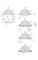
図4(a)の切断面図を用いて、説明に用いる各面を定義する。P1は、第2のコンデンサレンズ45の平面部である。P2は、熱伝導部材112の面であって、蛍光体51側の面である。P3は、蛍光体51の面であって、第2のコンデンサレンズ45および、熱伝導部材112の面である。 Each surface used for explanation is defined using the cross-sectional view of FIG. 4(a). P1 is the plane portion of the second condenser lens 45 . P2 is the surface of the heat-conducting member 112 and the surface on the phosphor 51 side. P3 is the surface of the phosphor 51 and is the surface on the side of the second condenser lens 45 and the heat conducting member 112 .

本実施例では、前述のように熱伝導部材112は第2のコンデンサレンズ45の平面部P1に対して凸あるいは凹にならないように一体成型される。また、図4(a)に示すように予め第2のコンデンサレンズ45は熱伝導部材112の厚み分の凹部(リセス)Rを形成しておき、凹部Rに熱伝導部材112を配置しても、貼り付けてもかまわない。何れの方法によっても、本実施例においては図4(b)に示すように、第2のコンデンサレンズ45の平面部P1、熱伝導部材112の面P2が同一の面CPになる構成であり、面CPは蛍光体51の面P3と面接触する。 In this embodiment, as described above, the heat conducting member 112 is integrally molded with respect to the plane portion P1 of the second condenser lens 45 so as not to be convex or concave. Alternatively, as shown in FIG. 4A, the second condenser lens 45 may be provided with a recess R corresponding to the thickness of the heat conducting member 112 in advance, and the heat conducting member 112 may be placed in the recess R. , can be pasted. By either method, as shown in FIG. 4B, in this embodiment, the plane portion P1 of the second condenser lens 45 and the plane P2 of the heat conducting member 112 are configured to be the same plane CP, Surface CP is in surface contact with surface P3 of phosphor 51 .

(変形例)
次に、図4(c)(d)の切断面図を用いて本実実施形態の第2のコンデンサレンズ45と蛍光体51と熱伝伝導材112の熱接触の構成についての別の形態を説明する。
(Modification)
4(c) and 4(d), another configuration of thermal contact between the second condenser lens 45, the phosphor 51, and the thermally conductive material 112 of this embodiment will be described. explain.

第2のコンデンサレンズ45と蛍光体51とは、図4(b)に示したような面接触する構成のみならず、図4(c)に示すように第2のコンデンサレンズ45の平面部P1と熱伝導部材112の面P2との間には隙間が設けられていてもよい。図4(c)は、前者の平面部P1および面P2に隙間δ1のある形態の模式図を示している。 The second condenser lens 45 and the phosphor 51 are not only in surface contact as shown in FIG. and the surface P2 of the heat conducting member 112 may be provided with a gap. FIG. 4(c) shows a schematic diagram of the form having a gap δ1 between the plane portion P1 and the surface P2 of the former.

図4(c)は、例えば熱伝導部材112を(蛍光体51に対して第2のコンデンサレンズ45が浮かない程度に)薄いシート状の形状で設け、当該熱伝導部材112を平坦な面を有する第2のコンデンサレンズと蛍光体51とで挟持して設けている。すなわち、シート(あるいは蛍光体51、第2のコンデンサレンズ45の密着部)の柔軟性で、実質的に蛍光体51に対して第2のコンデンサレンズ45が近くに配置することができる。図4(c)の段差δ1は、熱伝導部材112の厚みと等しくなるが、このδ1が、好ましくは100μm以下、より好ましくは10μm以下が望ましい。あるいは熱伝導部材112が厚みを有する部材であっても比較的柔軟に変形が可能であり、熱伝導部材112および第2のコンデンサレンズ45と、蛍光体51とが極力面接触に近い距離に構成することが好ましい。 In FIG. 4C, for example, the heat conduction member 112 is provided in a thin sheet shape (to the extent that the second condenser lens 45 does not float on the phosphor 51), and the heat conduction member 112 has a flat surface. It is sandwiched between the second condenser lens and the phosphor 51 provided. That is, the second condenser lens 45 can be substantially arranged close to the phosphor 51 due to the flexibility of the sheet (or the adhesion portion between the phosphor 51 and the second condenser lens 45 ). The step δ1 in FIG. 4C is equal to the thickness of the heat conducting member 112, and it is desirable that this δ1 be 100 μm or less, more preferably 10 μm or less. Alternatively, even if the heat-conducting member 112 is a thick member, it can be relatively flexibly deformed, and the heat-conducting member 112, the second condenser lens 45, and the phosphor 51 are arranged at a distance as close to surface contact as possible. preferably.

なお図4(c)の形態の場合には、熱伝導部材112と蛍光体51のオーバーラップ量δ2(熱伝導部材112が第2のコンデンサレンズ45と蛍光体51の両方と接触している面積)を小さくすればより好ましい。このように構成することで、蛍光体51に対して第2のコンデンサレンズ45が浮かないように構成が可能である。ただし、図4(b)に示す形態のように平面部P1と面P2が同一平面を構成する場合であれば、オーバーラップ量が大きいほど熱伝達の効率は向上することになる。もしくは、蛍光体51の面P3が、熱伝導部材112の逃げ形状(例えば熱伝導部材112の厚み分の凹面や、面取り形状等)を有しており、蛍光体51の面と第2のコンデンサレンズ45の平面部が面接触する形態もあり得る。 4(c), the overlap amount δ2 between the heat conducting member 112 and the phosphor 51 (the area where the heat conducting member 112 is in contact with both the second condenser lens 45 and the phosphor 51 ) is smaller. With this configuration, it is possible to configure so that the second condenser lens 45 does not float with respect to the phosphor 51 . However, in the case where the plane portion P1 and the plane P2 form the same plane as in the embodiment shown in FIG. 4B, the greater the amount of overlap, the more the heat transfer efficiency is improved. Alternatively, the surface P3 of the phosphor 51 has a relief shape of the heat conduction member 112 (for example, a concave surface corresponding to the thickness of the heat conduction member 112, a chamfered shape, etc.), and the surface of the phosphor 51 and the second capacitor are separated. A form in which the plane portions of the lens 45 are in surface contact is also possible.

また、第2のコンデンサレンズ45と蛍光体51とは、図4(d)に示すように蛍光体51に面取り形状Cを設け、形状Cの面で放熱部材112と接する構成にしてもよい。さらに、図4(e)に示すように蛍光体51の側面で熱伝導部材112が接触するような構成にしてもよい。このように熱伝導部材112を設けたとしても蛍光体51と熱伝導部材112とが接する領域が設けられているため、蛍光体51の熱を良好に熱伝導部材112へと放熱させることができる。そして熱伝導部材112と第2のコンデンサレンズ45とが接するようにも設けられているため、蛍光体51から第2のコンデンサレンズ45へと伝わった熱も、熱伝導部材112へと放熱させることができる。 Further, the second condenser lens 45 and the phosphor 51 may be arranged such that the chamfered shape C is provided on the phosphor 51 as shown in FIG. Furthermore, as shown in FIG. 4(e), a structure may be adopted in which the heat conducting member 112 is in contact with the side surface of the phosphor 51. FIG. Even if the heat-conducting member 112 is provided in this way, the heat of the phosphor 51 can be efficiently radiated to the heat-conducting member 112 because there is provided a region where the phosphor 51 and the heat-conducting member 112 are in contact with each other. . Since the heat-conducting member 112 and the second condenser lens 45 are also provided so as to be in contact with each other, the heat transmitted from the phosphor 51 to the second condenser lens 45 can also be dissipated to the heat-conducting member 112 . can be done.

なお蛍光体51は、結晶状の形態や、粉末状の蛍光体をいわゆるバインダーと称される樹脂部材により、基材に固着(塗布)させた形態があり得る。この場合、基材の領域、あるいは蛍光体粉末を含まない(少ない)領域に逃げ形状を設けると、蛍光変換の効率を損なわず好ましい。 The phosphor 51 may be in a crystalline form or in a form in which a powdery phosphor is fixed (applied) to a base material by a resin member called a so-called binder. In this case, it is preferable to provide relief shapes in areas of the base material or in areas that do not contain (small amount) phosphor powder, as this does not impair the efficiency of fluorescence conversion.

(実施例2)
以下、図5、および図6を参照しながら蛍光体51を効率的に冷却できる第2の実施例による投射型表示装置10について説明する。実施例1と同様の構成には同一の符号を付し、説明は省略する。
(Example 2)
A projection display apparatus 10 according to a second embodiment capable of efficiently cooling the phosphor 51 will be described below with reference to FIGS. 5 and 6. FIG. The same reference numerals are assigned to the same configurations as in the first embodiment, and the description thereof is omitted.

図5は、実施例2に係る蛍光体51の周囲の構成の断面図である。図6は、実施例2に係る蛍光体51の周囲の構成を、光源からのレーザー光100が入射する向きから見た図である。 FIG. 5 is a cross-sectional view of the configuration around the phosphor 51 according to the second embodiment. FIG. 6 is a view of the configuration around the phosphor 51 according to Example 2, viewed from the direction in which the laser beam 100 from the light source is incident.

図5に示すように、実施例2では放熱部材110に加えて、保持部材111の側面に放熱部材120を設けている。 As shown in FIG. 5, in addition to the heat radiating member 110, the heat radiating member 120 is provided on the side surface of the holding member 111 in the second embodiment.

実施例2における熱伝導部材212の延出部212bは、実施例1と同様に、放熱部材110と保持部材111に狭持されて保持される。これにより第2のコンデンサレンズ45と蛍光体51の周囲の密閉性を保ちつつ、蛍光体51の熱を放熱部材110および保持部材111に効率的に伝導することが可能となる。 The extending portion 212b of the heat conducting member 212 in the second embodiment is sandwiched and held between the heat radiating member 110 and the holding member 111, as in the first embodiment. As a result, the heat of the phosphor 51 can be efficiently conducted to the heat radiating member 110 and the holding member 111 while maintaining the airtightness around the second condenser lens 45 and the phosphor 51 .

加えて実施例2における熱伝導部材212は、延出部212bからさらに、保持部材111の側面に沿うように延設された延出部212cを有する。 In addition, the heat-conducting member 212 in Example 2 has an extending portion 212c extending along the side surface of the holding member 111 from the extending portion 212b.

延出部212cは、保持部材111および放熱部材120とで狭持される構成である。この構成によって、蛍光体51の熱を放熱部材120にも伝導することができる。すなわち、より高い効率で蛍光体51を冷却することができる。 The extending portion 212c is configured to be sandwiched between the holding member 111 and the heat radiating member 120 . With this configuration, the heat of the phosphor 51 can also be conducted to the heat dissipation member 120 . That is, the phosphor 51 can be cooled with higher efficiency.

以上説明したように、本実施例の構成によれば、蛍光体への塵埃の付着を防止するために蛍光体まわりの密閉性を保ちつつ、コンデンサレンズ側からの冷却の効率を、従来の構成より向上させることができる。 As described above, according to the configuration of the present embodiment, the efficiency of cooling from the condenser lens side can be improved compared to the conventional configuration, while maintaining the airtightness around the phosphor to prevent dust from adhering to the phosphor. can be improved.

また、熱伝導部材212の延出部を保持部材よりも延出させて、さらに新たな放熱部材(実施例2では放熱部材120)等を追加して、これらにも伝熱させることが出来るため、さらに冷却効率を向上することができる。 Further , the extending portion of the heat conducting member 212 can be made to extend beyond the holding member, and a new heat radiating member (the heat radiating member 120 in the second embodiment) can be added to transfer heat to these members as well. Therefore, the cooling efficiency can be further improved.

(実施例1、2共通の変形例)
以上、本発明の好ましい実施形態について説明したが、本発明はこれらの実施形態に限定されず、その要旨の範囲内で種々の変形および変更が可能である。
(Modified Example Common to Embodiments 1 and 2)
Although preferred embodiments of the present invention have been described above, the present invention is not limited to these embodiments, and various modifications and changes are possible within the scope of the gist.

例えば、本実施形態において熱伝導部材212はグラファイトシートで形成されるとしたが、実使用上はこれによらず熱伝導率の高い金属メッシュやヒートパイプなどで構成されてもよい。 For example, in the present embodiment , the heat -conducting member 212 is made of a graphite sheet.

また、蛍光体は低融点ガラスによって形成(基材に固着)されている。この低融点ガラスを、コンデンサレンズを保持可能に形成することで、保持部材と蛍光体が一体となるように構成してもよい。すなわち、保持部材は蛍光体を形成する低融点ガラスによって形成されてもよい。 Also, the phosphor is formed (fixed to the substrate) by low-melting-point glass. By forming the low-melting-point glass so as to be able to hold the condenser lens, the holding member and the phosphor may be integrated. That is, the holding member may be made of low-melting-point glass that forms the phosphor.

45 第2のコンデンサレンズ
51 蛍光体
110、120 放熱部材
111 保持部材
112 熱伝導部材
112b 延出部
45 Second Condenser Lens 51 Phosphor 110, 120 Heat Dissipating Member 111 Holding Member 112 Heat Conducting Member 112b Extension

Claims (11)

光源からの光の波長を変換する蛍光体を備える波長変換素子と、
該波長変換素子に前記光源からの光を集光させる集光部材と、
前記集光部材よりも熱伝導率が大きい熱伝導部材を有し、
前記集光部材は、前記熱伝導部材を介さずに前記波長変換素子と対向する透過部と、前記波長変換素子に対する間隔が前記透過部よりも広い凹部を含み、
前記蛍光体と前記熱伝導部材前記凹部とは、前記集光部材の光軸方向から見たときに少なくとも一部がこの順に重なって配置され
前記蛍光体と前記熱伝導部材の少なくとも一部が接触していることを特徴とする光源装置。
a wavelength conversion element comprising a phosphor that converts the wavelength of light from a light source;
a condensing member for condensing light from the light source onto the wavelength conversion element;
Having a thermally conductive member having a higher thermal conductivity than the light collecting member,
the light-condensing member includes a transmissive portion facing the wavelength conversion element without interposing the heat-conducting member, and a concave portion having a wider distance from the wavelength conversion element than the transmissive portion;
the phosphor, the heat-conducting member , and the concave portion are arranged so that at least a portion thereof overlaps in this order when viewed from the optical axis direction of the condensing member ;
A light source device , wherein at least a part of the phosphor and the thermally conductive member are in contact with each other.
前記波長変換素子と前記透過部が接するように設けられていることを特徴とする請求項1に記載の光源装置。 2. The light source device according to claim 1, wherein said wavelength conversion element and said transmission portion are provided so as to be in contact with each other. 前記波長変換素子と前記凹部の間隔は、100μm以下であることを特徴とする請求項1に記載の光源装置。 2. The light source device according to claim 1, wherein the distance between said wavelength conversion element and said concave portion is 100 [mu]m or less. 前記熱伝導部材は、前記集光部材の光軸方向からみたときに、
前記光源からの光が透過する前記透過部を囲むように設けられていることを特徴とする請求項1乃至3のいずれか1項に記載の光源装置。
When viewed from the optical axis direction of the light-condensing member, the heat-conducting member has
4. The light source device according to any one of claims 1 to 3, wherein the light source device is provided so as to surround the transmission portion through which the light from the light source is transmitted.
前記波長変換素子は、前記集光部材を含む複数の部材で囲まれて形成された空間に配置されており、前記熱伝導部材は当該空間の外部に延出するように設けられていることを特徴とする請求項1乃至4のいずれか1項に記載の光源装置。 The wavelength conversion element is arranged in a space formed by being surrounded by a plurality of members including the light collecting member, and the heat conducting member is provided so as to extend outside the space. 5. A light source device according to any one of claims 1 to 4. 前記波長変換素子は放熱部材の上に設けられており、前記熱伝導部材の前記空間の外部に延出した部分は、前記放熱部材に接するように設けられていることを特徴とする請求項5に記載の光源装置。 5. The wavelength conversion element is provided on a heat radiating member, and the portion of the heat conducting member which extends outside the space is provided so as to be in contact with the heat radiating member. The light source device according to . 前記熱伝導部材の径方向の大きさは、前記集光部材の径方向の大きさよりも大きいことを特徴とする請求項1乃至6のいずれか1項に記載の光源装置。 7. The light source device according to any one of claims 1 to 6, wherein the radial size of the heat conducting member is larger than the radial size of the condensing member. 記蛍光体に前記光源からの光が入射するように、前記熱伝導部材には開口が設けられていることを特徴とする請求項1乃至7のいずれか1項に記載の光源装置。 8. The light source device according to any one of claims 1 to 7, wherein an opening is provided in said heat conducting member so that light from said light source is incident on said phosphor. 前記熱伝導部材の前記開口の大きさは前記蛍光体の外形よりも小さいことを特徴とする請求項8に記載の光源装置。 9. The light source device according to claim 8, wherein the size of said opening of said heat conducting member is smaller than the outline of said phosphor. 前記波長変換素子は反射層を有し、前記反射層と前記熱伝導部材の間に前記蛍光体が配置されていることを特徴とする請求項1乃至9のいずれか1項に記載の光源装置。 10. The light source according to any one of claims 1 to 9, wherein the wavelength conversion element has a reflective layer, and the phosphor is arranged between the reflective layer and the heat-conducting member. Device. 請求項1乃至10のいずれか1項に記載の光源装置と、該光源装置からの光を変調する光変調素子と、前記光源装置からの光により前記光変調素子を照明する照明光学系と、を有し、前記光変調素子からの光を投射することを特徴とする投射型表示装置。 The light source device according to any one of claims 1 to 10, a light modulation element that modulates light from the light source device, and an illumination optical system that illuminates the light modulation device with the light from the light source device, and projecting the light from the light modulation element.
JP2018157277A 2017-11-22 2018-08-24 Light source device and projection display device having the same Active JP7207903B2 (en)

Priority Applications (1)

Application Number Priority Date Filing Date Title
US16/192,519 US10567717B2 (en) 2017-11-22 2018-11-15 Light source device and projection type display apparatus including light source device

Applications Claiming Priority (2)

Application Number Priority Date Filing Date Title
JP2017225128 2017-11-22

Publications (3)

Publication Number Publication Date
JP2019095771A JP2019095771A (en) 2019-06-20
JP2019095771A5 JP2019095771A5 (en) 2021-11-11
JP7207903B2 true JP7207903B2 (en) 2023-01-18

Family

ID=66972986

Family Applications (1)

Application Number Title Priority Date Filing Date
JP2018157277A Active JP7207903B2 (en) 2017-11-22 2018-08-24 Light source device and projection display device having the same

Country Status (1)

Country Link
JP (1) JP7207903B2 (en)

Families Citing this family (4)

* Cited by examiner, † Cited by third party
Publication number Priority date Publication date Assignee Title
JP7279571B2 (en) * 2019-08-06 2023-05-23 セイコーエプソン株式会社 Light source device and projector
JP7230732B2 (en) 2019-08-06 2023-03-01 セイコーエプソン株式会社 Light source device and projector
JP2021120728A (en) * 2020-01-31 2021-08-19 カシオ計算機株式会社 Fluorescence emission device, light source device and projection device
CN114967305A (en) * 2022-06-29 2022-08-30 歌尔光学科技有限公司 Flexible heat radiation fin

Citations (9)

* Cited by examiner, † Cited by third party
Publication number Priority date Publication date Assignee Title
CN201820786U (en) 2010-08-12 2011-05-04 红蝶科技(深圳)有限公司 Efficient monochromatic light source packaging structure with excitation cavity and optical projection engine
JP2012226986A (en) 2011-04-20 2012-11-15 Stanley Electric Co Ltd Light source device and lighting system
CN103647011A (en) 2013-12-18 2014-03-19 吴震 Light-emitting diode encapsulation structure and light emitting device
JP2014123014A (en) 2012-12-21 2014-07-03 Casio Comput Co Ltd Light source device, projector
JP2015230354A (en) 2014-06-04 2015-12-21 セイコーエプソン株式会社 Light source device and projector
WO2016156399A1 (en) 2015-04-01 2016-10-06 Philips Lighting Holding B.V. High brightness light emitting apparatus
WO2016185850A1 (en) 2015-05-15 2016-11-24 ソニー株式会社 Optical conversion device, light source device, and projector
JP2017021100A (en) 2015-07-08 2017-01-26 セイコーエプソン株式会社 Wavelength conversion element, method for manufacturing wavelength conversion element, illumination device and projector
JP2017142479A (en) 2016-02-05 2017-08-17 セイコーエプソン株式会社 Wavelength conversion element, light source device, and projector

Patent Citations (9)

* Cited by examiner, † Cited by third party
Publication number Priority date Publication date Assignee Title
CN201820786U (en) 2010-08-12 2011-05-04 红蝶科技(深圳)有限公司 Efficient monochromatic light source packaging structure with excitation cavity and optical projection engine
JP2012226986A (en) 2011-04-20 2012-11-15 Stanley Electric Co Ltd Light source device and lighting system
JP2014123014A (en) 2012-12-21 2014-07-03 Casio Comput Co Ltd Light source device, projector
CN103647011A (en) 2013-12-18 2014-03-19 吴震 Light-emitting diode encapsulation structure and light emitting device
JP2015230354A (en) 2014-06-04 2015-12-21 セイコーエプソン株式会社 Light source device and projector
WO2016156399A1 (en) 2015-04-01 2016-10-06 Philips Lighting Holding B.V. High brightness light emitting apparatus
WO2016185850A1 (en) 2015-05-15 2016-11-24 ソニー株式会社 Optical conversion device, light source device, and projector
JP2017021100A (en) 2015-07-08 2017-01-26 セイコーエプソン株式会社 Wavelength conversion element, method for manufacturing wavelength conversion element, illumination device and projector
JP2017142479A (en) 2016-02-05 2017-08-17 セイコーエプソン株式会社 Wavelength conversion element, light source device, and projector

Also Published As

Publication number Publication date
JP2019095771A (en) 2019-06-20

Similar Documents

Publication Publication Date Title
JP7207903B2 (en) Light source device and projection display device having the same
JP6737265B2 (en) Light conversion device, light source device, and projector
US10136111B2 (en) Wavelength converter, illuminator, and projector
US10712648B2 (en) Wavelength-converting wheel and projection apparatus
JPWO2016056285A1 (en) Phosphor wheel, light source device, and projection display device
JP6939805B2 (en) Light source device and projection type display device
JP7124831B2 (en) WAVELENGTH CONVERTER AND PROJECTION DISPLAY DEVICE
WO2016181768A1 (en) Fluorescent substrate, light source device, and projection-type display device
US20180149954A1 (en) Wavelength conversion element, light source apparatus, and projector
US11092799B2 (en) Phosphor wheel apparatus, lighting apparatus, and projection type image display apparatus
JP2017151250A (en) Wavelength conversion element, light source device, and projector
US10567717B2 (en) Light source device and projection type display apparatus including light source device
JP2019095771A5 (en)
CN113917774B (en) Projector with a light source for projecting light
US20110057557A1 (en) Projection led module and method of making a projection led module
JPWO2016185860A1 (en) Phosphor substrate, light source device, and projection display device
TW201833656A (en) Image display device and light source device
JP2007086140A (en) Liquid crystal projector
CN113671779B (en) Light source device and projection device
JP2018132746A (en) Optical unit and light source device using the same, and projection type display device
US11688834B2 (en) Wavelength conversion member and light-emitting device for efficient wavelength conversion
JP7306538B2 (en) projector
JP5879707B2 (en) Reflective liquid crystal display device and projection display device

Legal Events

Date Code Title Description
A521 Request for written amendment filed

Free format text: JAPANESE INTERMEDIATE CODE: A523

Effective date: 20210811

A621 Written request for application examination

Free format text: JAPANESE INTERMEDIATE CODE: A621

Effective date: 20210811

A977 Report on retrieval

Free format text: JAPANESE INTERMEDIATE CODE: A971007

Effective date: 20220530

A131 Notification of reasons for refusal

Free format text: JAPANESE INTERMEDIATE CODE: A131

Effective date: 20220607

A521 Request for written amendment filed

Free format text: JAPANESE INTERMEDIATE CODE: A523

Effective date: 20220801

A131 Notification of reasons for refusal

Free format text: JAPANESE INTERMEDIATE CODE: A131

Effective date: 20220906

A521 Request for written amendment filed

Free format text: JAPANESE INTERMEDIATE CODE: A523

Effective date: 20221107

TRDD Decision of grant or rejection written
A01 Written decision to grant a patent or to grant a registration (utility model)

Free format text: JAPANESE INTERMEDIATE CODE: A01

Effective date: 20221206

A61 First payment of annual fees (during grant procedure)

Free format text: JAPANESE INTERMEDIATE CODE: A61

Effective date: 20230105

R151 Written notification of patent or utility model registration

Ref document number: 7207903

Country of ref document: JP

Free format text: JAPANESE INTERMEDIATE CODE: R151