JP7202971B2 - Evaporation Source Apparatus, Film Forming Apparatus, Film Forming Method, and Electronic Device Manufacturing Method - Google Patents
Evaporation Source Apparatus, Film Forming Apparatus, Film Forming Method, and Electronic Device Manufacturing Method Download PDFInfo
- Publication number
- JP7202971B2 JP7202971B2 JP2019099034A JP2019099034A JP7202971B2 JP 7202971 B2 JP7202971 B2 JP 7202971B2 JP 2019099034 A JP2019099034 A JP 2019099034A JP 2019099034 A JP2019099034 A JP 2019099034A JP 7202971 B2 JP7202971 B2 JP 7202971B2
- Authority
- JP
- Japan
- Prior art keywords
- heater
- region
- evaporation source
- source device
- vapor deposition
- Prior art date
- Legal status (The legal status is an assumption and is not a legal conclusion. Google has not performed a legal analysis and makes no representation as to the accuracy of the status listed.)
- Active
Links
- 238000001704 evaporation Methods 0.000 title claims description 110
- 230000008020 evaporation Effects 0.000 title claims description 108
- 238000000034 method Methods 0.000 title claims description 20
- 238000004519 manufacturing process Methods 0.000 title claims description 18
- 239000000463 material Substances 0.000 claims description 107
- 238000007740 vapor deposition Methods 0.000 claims description 85
- 238000010438 heat treatment Methods 0.000 claims description 60
- 230000015572 biosynthetic process Effects 0.000 claims description 22
- 230000007423 decrease Effects 0.000 claims description 12
- 238000001514 detection method Methods 0.000 claims description 9
- 239000010408 film Substances 0.000 description 58
- 239000000758 substrate Substances 0.000 description 52
- 239000010410 layer Substances 0.000 description 42
- 238000009826 distribution Methods 0.000 description 27
- 238000000151 deposition Methods 0.000 description 16
- 230000008021 deposition Effects 0.000 description 16
- 230000005525 hole transport Effects 0.000 description 8
- 239000002184 metal Substances 0.000 description 8
- 229910052751 metal Inorganic materials 0.000 description 8
- 238000010586 diagram Methods 0.000 description 6
- 230000006870 function Effects 0.000 description 6
- 230000002093 peripheral effect Effects 0.000 description 6
- 238000003860 storage Methods 0.000 description 6
- 230000007246 mechanism Effects 0.000 description 5
- 239000010409 thin film Substances 0.000 description 5
- QVGXLLKOCUKJST-UHFFFAOYSA-N atomic oxygen Chemical compound [O] QVGXLLKOCUKJST-UHFFFAOYSA-N 0.000 description 4
- 230000000052 comparative effect Effects 0.000 description 4
- 239000001301 oxygen Substances 0.000 description 4
- 229910052760 oxygen Inorganic materials 0.000 description 4
- 238000001816 cooling Methods 0.000 description 3
- 230000006866 deterioration Effects 0.000 description 3
- 230000005484 gravity Effects 0.000 description 3
- 239000011810 insulating material Substances 0.000 description 3
- 239000011368 organic material Substances 0.000 description 3
- 239000011241 protective layer Substances 0.000 description 3
- 239000004925 Acrylic resin Substances 0.000 description 2
- 229920000178 Acrylic resin Polymers 0.000 description 2
- 239000011261 inert gas Substances 0.000 description 2
- 239000012044 organic layer Substances 0.000 description 2
- 238000003825 pressing Methods 0.000 description 2
- IJGRMHOSHXDMSA-UHFFFAOYSA-N Atomic nitrogen Chemical compound N#N IJGRMHOSHXDMSA-UHFFFAOYSA-N 0.000 description 1
- 238000007630 basic procedure Methods 0.000 description 1
- 239000003575 carbonaceous material Substances 0.000 description 1
- 239000000919 ceramic Substances 0.000 description 1
- 230000008859 change Effects 0.000 description 1
- 210000000078 claw Anatomy 0.000 description 1
- 238000010549 co-Evaporation Methods 0.000 description 1
- 239000000470 constituent Substances 0.000 description 1
- 239000013078 crystal Substances 0.000 description 1
- 230000003247 decreasing effect Effects 0.000 description 1
- 230000007547 defect Effects 0.000 description 1
- 229910001873 dinitrogen Inorganic materials 0.000 description 1
- 238000006073 displacement reaction Methods 0.000 description 1
- 230000000694 effects Effects 0.000 description 1
- 239000007772 electrode material Substances 0.000 description 1
- 238000005401 electroluminescence Methods 0.000 description 1
- 238000005516 engineering process Methods 0.000 description 1
- 239000007789 gas Substances 0.000 description 1
- 239000011521 glass Substances 0.000 description 1
- 238000003384 imaging method Methods 0.000 description 1
- 229910010272 inorganic material Inorganic materials 0.000 description 1
- 239000011147 inorganic material Substances 0.000 description 1
- 238000011835 investigation Methods 0.000 description 1
- 238000001459 lithography Methods 0.000 description 1
- 239000011159 matrix material Substances 0.000 description 1
- 229910044991 metal oxide Inorganic materials 0.000 description 1
- 150000004706 metal oxides Chemical class 0.000 description 1
- 150000002739 metals Chemical class 0.000 description 1
- 230000003287 optical effect Effects 0.000 description 1
- 238000013021 overheating Methods 0.000 description 1
- 230000000704 physical effect Effects 0.000 description 1
- 238000005268 plasma chemical vapour deposition Methods 0.000 description 1
- 230000008569 process Effects 0.000 description 1
- 230000005855 radiation Effects 0.000 description 1
- 230000009467 reduction Effects 0.000 description 1
- 239000011347 resin Substances 0.000 description 1
- 229920005989 resin Polymers 0.000 description 1
- 238000004528 spin coating Methods 0.000 description 1
- 238000004544 sputter deposition Methods 0.000 description 1
- 238000012546 transfer Methods 0.000 description 1
- 238000001771 vacuum deposition Methods 0.000 description 1
- 238000005019 vapor deposition process Methods 0.000 description 1
- 238000009834 vaporization Methods 0.000 description 1
- 230000008016 vaporization Effects 0.000 description 1
Images


Classifications
-
- C—CHEMISTRY; METALLURGY
- C23—COATING METALLIC MATERIAL; COATING MATERIAL WITH METALLIC MATERIAL; CHEMICAL SURFACE TREATMENT; DIFFUSION TREATMENT OF METALLIC MATERIAL; COATING BY VACUUM EVAPORATION, BY SPUTTERING, BY ION IMPLANTATION OR BY CHEMICAL VAPOUR DEPOSITION, IN GENERAL; INHIBITING CORROSION OF METALLIC MATERIAL OR INCRUSTATION IN GENERAL
- C23C—COATING METALLIC MATERIAL; COATING MATERIAL WITH METALLIC MATERIAL; SURFACE TREATMENT OF METALLIC MATERIAL BY DIFFUSION INTO THE SURFACE, BY CHEMICAL CONVERSION OR SUBSTITUTION; COATING BY VACUUM EVAPORATION, BY SPUTTERING, BY ION IMPLANTATION OR BY CHEMICAL VAPOUR DEPOSITION, IN GENERAL
- C23C14/00—Coating by vacuum evaporation, by sputtering or by ion implantation of the coating forming material
- C23C14/22—Coating by vacuum evaporation, by sputtering or by ion implantation of the coating forming material characterised by the process of coating
- C23C14/54—Controlling or regulating the coating process
- C23C14/542—Controlling the film thickness or evaporation rate
- C23C14/543—Controlling the film thickness or evaporation rate using measurement on the vapor source
-
- C—CHEMISTRY; METALLURGY
- C23—COATING METALLIC MATERIAL; COATING MATERIAL WITH METALLIC MATERIAL; CHEMICAL SURFACE TREATMENT; DIFFUSION TREATMENT OF METALLIC MATERIAL; COATING BY VACUUM EVAPORATION, BY SPUTTERING, BY ION IMPLANTATION OR BY CHEMICAL VAPOUR DEPOSITION, IN GENERAL; INHIBITING CORROSION OF METALLIC MATERIAL OR INCRUSTATION IN GENERAL
- C23C—COATING METALLIC MATERIAL; COATING MATERIAL WITH METALLIC MATERIAL; SURFACE TREATMENT OF METALLIC MATERIAL BY DIFFUSION INTO THE SURFACE, BY CHEMICAL CONVERSION OR SUBSTITUTION; COATING BY VACUUM EVAPORATION, BY SPUTTERING, BY ION IMPLANTATION OR BY CHEMICAL VAPOUR DEPOSITION, IN GENERAL
- C23C14/00—Coating by vacuum evaporation, by sputtering or by ion implantation of the coating forming material
- C23C14/22—Coating by vacuum evaporation, by sputtering or by ion implantation of the coating forming material characterised by the process of coating
- C23C14/24—Vacuum evaporation
- C23C14/243—Crucibles for source material
-
- C—CHEMISTRY; METALLURGY
- C23—COATING METALLIC MATERIAL; COATING MATERIAL WITH METALLIC MATERIAL; CHEMICAL SURFACE TREATMENT; DIFFUSION TREATMENT OF METALLIC MATERIAL; COATING BY VACUUM EVAPORATION, BY SPUTTERING, BY ION IMPLANTATION OR BY CHEMICAL VAPOUR DEPOSITION, IN GENERAL; INHIBITING CORROSION OF METALLIC MATERIAL OR INCRUSTATION IN GENERAL
- C23C—COATING METALLIC MATERIAL; COATING MATERIAL WITH METALLIC MATERIAL; SURFACE TREATMENT OF METALLIC MATERIAL BY DIFFUSION INTO THE SURFACE, BY CHEMICAL CONVERSION OR SUBSTITUTION; COATING BY VACUUM EVAPORATION, BY SPUTTERING, BY ION IMPLANTATION OR BY CHEMICAL VAPOUR DEPOSITION, IN GENERAL
- C23C14/00—Coating by vacuum evaporation, by sputtering or by ion implantation of the coating forming material
- C23C14/22—Coating by vacuum evaporation, by sputtering or by ion implantation of the coating forming material characterised by the process of coating
- C23C14/24—Vacuum evaporation
- C23C14/26—Vacuum evaporation by resistance or inductive heating of the source
-
- C—CHEMISTRY; METALLURGY
- C23—COATING METALLIC MATERIAL; COATING MATERIAL WITH METALLIC MATERIAL; CHEMICAL SURFACE TREATMENT; DIFFUSION TREATMENT OF METALLIC MATERIAL; COATING BY VACUUM EVAPORATION, BY SPUTTERING, BY ION IMPLANTATION OR BY CHEMICAL VAPOUR DEPOSITION, IN GENERAL; INHIBITING CORROSION OF METALLIC MATERIAL OR INCRUSTATION IN GENERAL
- C23C—COATING METALLIC MATERIAL; COATING MATERIAL WITH METALLIC MATERIAL; SURFACE TREATMENT OF METALLIC MATERIAL BY DIFFUSION INTO THE SURFACE, BY CHEMICAL CONVERSION OR SUBSTITUTION; COATING BY VACUUM EVAPORATION, BY SPUTTERING, BY ION IMPLANTATION OR BY CHEMICAL VAPOUR DEPOSITION, IN GENERAL
- C23C14/00—Coating by vacuum evaporation, by sputtering or by ion implantation of the coating forming material
- C23C14/22—Coating by vacuum evaporation, by sputtering or by ion implantation of the coating forming material characterised by the process of coating
- C23C14/54—Controlling or regulating the coating process
-
- H—ELECTRICITY
- H10—SEMICONDUCTOR DEVICES; ELECTRIC SOLID-STATE DEVICES NOT OTHERWISE PROVIDED FOR
- H10K—ORGANIC ELECTRIC SOLID-STATE DEVICES
- H10K71/00—Manufacture or treatment specially adapted for the organic devices covered by this subclass
-
- H—ELECTRICITY
- H10—SEMICONDUCTOR DEVICES; ELECTRIC SOLID-STATE DEVICES NOT OTHERWISE PROVIDED FOR
- H10K—ORGANIC ELECTRIC SOLID-STATE DEVICES
- H10K71/00—Manufacture or treatment specially adapted for the organic devices covered by this subclass
- H10K71/10—Deposition of organic active material
- H10K71/16—Deposition of organic active material using physical vapour deposition [PVD], e.g. vacuum deposition or sputtering
- H10K71/164—Deposition of organic active material using physical vapour deposition [PVD], e.g. vacuum deposition or sputtering using vacuum deposition
Description
本発明は、蒸発源装置、成膜装置、成膜方法および電子デバイスの製造方法に関する。 The present invention relates to an evaporation source device, a film forming apparatus, a film forming method, and an electronic device manufacturing method.
近年、ディスプレイの一種として、有機材料の電界発光を用いた有機EL素子を備えた有機EL装置が注目を集めている。かかる有機ELディスプレイ等の有機電子デバイス製造において、蒸発源装置を用いて、基板上に有機材料や金属電極材料などの蒸着材料を蒸着させて成膜を行う工程がある。 2. Description of the Related Art In recent years, as a type of display, an organic EL device having an organic EL element using electroluminescence of an organic material has been attracting attention. In the manufacture of organic electronic devices such as organic EL displays, there is a step of forming a film by evaporating an evaporation material such as an organic material or a metal electrode material on a substrate using an evaporation source device.
蒸着工程で用いられる蒸発源装置は、蒸着材料が収容される容器としての機能と、蒸着材料の温度を上昇させて蒸発させ、基板の表面に付着させるための加熱機能を有する。従来の蒸発源装置としては、例えば、特許文献1に記載されているように、容器の上部を加熱する上部ヒータ(第1ヒータ)と、坩堝の下部を加熱する下部ヒータ(第2ヒータ)と、を有し、2つのヒータを独立に加熱制御するようにした蒸発源装置が知られている。 The evaporation source device used in the vapor deposition process has a function as a container for storing the vapor deposition material and a heating function for increasing the temperature of the vapor deposition material to evaporate it and adhere it to the surface of the substrate. As a conventional evaporation source device, for example, as described in Patent Document 1, an upper heater (first heater) for heating the upper part of the container and a lower heater (second heater) for heating the lower part of the crucible are used. , and independently heat-controls two heaters.
特許文献1のような2つのヒータを有する蒸発源装置を用いて蒸着を行う場合、容器の開口部への蒸着材料の付着を抑制するために、容器開口部付近は高温に保つことが好ましい。しかし、容器の開口部付近を高温に保ち、かつ蒸着レートを一定に保つようにヒータの加熱制御を行おうとすると、下部ヒータからの輻射熱が影響して容器坩堝の開口部付近の温度が過度に上昇して材料が劣化するおそれがある。そのため、下部ヒータからの輻射熱を考慮して上部ヒータを加熱制御する必要が生じ、各ヒータの加熱制御が複雑になるという課題が生じる。 When vapor deposition is performed using an evaporation source device having two heaters as in Patent Literature 1, it is preferable to keep the vicinity of the opening of the container at a high temperature in order to suppress adhesion of the vapor deposition material to the opening of the container. However, when trying to control the heating of the heater so as to maintain a high temperature around the opening of the container and keep the vapor deposition rate constant, the temperature around the opening of the container crucible becomes excessive due to the influence of radiant heat from the lower heater. It may rise and deteriorate the material. Therefore, it becomes necessary to control the heating of the upper heaters in consideration of the radiant heat from the lower heaters.
本発明は上記課題を解決するためになされたもので、その目的は、簡便な制御で、容器の開口部付近を、過度な温度上昇を抑制しつつ高温に保ったまま、蒸発レートを一定に保つように制御することができる蒸発源装置、成膜装置、成膜方法および電子デバイスの製造方法を提供することにある。 The present invention was made in order to solve the above problems, and its purpose is to keep the evaporation rate constant while suppressing excessive temperature rise and keeping the vicinity of the opening of the container at a high temperature with simple control. An object of the present invention is to provide an evaporation source apparatus, a film forming apparatus, a film forming method, and an electronic device manufacturing method that can be controlled to maintain the
上記目的を達成するために、本発明の第1の蒸発源装置は、蒸着材料を収容した容器を加熱して被蒸着体に前記蒸着材料の蒸着を行う蒸発源装置であって、
前記容器は、加熱された蒸着材料が放出される開口部と、第1領域と、前記第1領域よりも前記開口部から離れた領域である第2領域と、を有し、
前記第1領域を加熱する第1ヒータと、
前記第2領域を加熱する第2ヒータと、
前記第1ヒータと前記第2ヒータをそれぞれ独立に制御する制御部と、
前記第1ヒータと前記第2ヒータとの間に配置され、前記第1ヒータからの熱の少なくとも一部を反射する中間反射部材と、を有し、
前記制御部は、前記容器に収容された蒸着材料の減少に伴って、前記第2ヒータに投入する電力を上げることを特徴とする。
In order to achieve the above object, a first evaporation source device of the present invention is an evaporation source device for heating a container containing an evaporation material to deposit the evaporation material on an object to be evaporated,
The container has an opening from which heated vapor deposition material is discharged, a first region, and a second region that is a region further from the opening than the first region,
a first heater that heats the first region;
a second heater that heats the second region;
a control unit that independently controls the first heater and the second heater;
an intermediate reflecting member disposed between the first heater and the second heater and reflecting at least part of heat from the first heater;
The control unit is characterized in that the electric power supplied to the second heater is increased as the vapor deposition material contained in the container decreases.
また、本発明の第2の蒸発源装置は、蒸着材料を収容した容器を加熱して被蒸着体に前記蒸着材料の蒸着を行う蒸発源装置であって、
前記容器は、加熱された前記蒸着材料が放出される開口部と、第1領域と、前記第1領域よりも前記開口部から離れた領域である第2領域と、を有し、
前記第1領域を加熱する第1ヒータと、
前記第2領域を加熱する第2ヒータと、
前記第1ヒータと前記第2ヒータをそれぞれ独立に制御する制御部と、
前記第1ヒータと前記第2ヒータとの間に配置され、前記第1ヒータからの熱の少なくとも一部を反射する中間反射部材と、を有し、
前記制御部は、
前記第1ヒータに第1の電力を投入しつつ、前記第2ヒータに第2の電力を投入する第1の加熱制御と、
前記第1の加熱制御を行った後に、前記第1ヒータに前記第1の電力を投入しつつ、前記2ヒータに前記第2の電力よりも大きな第3の電力を投入する第2の加熱制御と、
を行うことを特徴とする。
A second evaporation source device of the present invention is an evaporation source device that heats a container containing a vapor deposition material to vapor-deposit the vapor deposition material on an object to be vapor-deposited ,
The container has an opening from which the heated vapor deposition material is discharged, a first region, and a second region that is a region further from the opening than the first region,
a first heater that heats the first region;
a second heater that heats the second region;
a control unit that independently controls the first heater and the second heater;
an intermediate reflecting member disposed between the first heater and the second heater and reflecting at least part of heat from the first heater;
The control unit
a first heating control of applying a second electric power to the second heater while applying a first electric power to the first heater;
After performing the first heating control, a second heating control in which the first electric power is applied to the first heater and a third electric power larger than the second electric power is applied to the two heaters. When,
characterized by performing
また、本発明の第1の成膜装置は、
蒸着材料を収容した容器を加熱する蒸発源装置であって、
前記容器は、加熱された蒸着材料が放出される開口部と、第1領域と、前記第1領域よりも前記開口部から離れた領域である第2領域と、を有し、
前記第1領域を加熱する第1ヒータと、
前記第2領域を加熱する第2ヒータと、
前記第1ヒータと前記第2ヒータをそれぞれ独立に制御する制御部と、
前記第1ヒータと前記第2ヒータとの間に配置され、前記第1ヒータからの熱の少なくとも一部を反射する中間反射部材と、を有し、
前記制御部は、前記容器に収容された蒸着材料の減少に伴って、前記第2ヒータに投入する電力を上げる蒸発源装置と、
前記蒸発源装置が配置され、前記蒸着材料の蒸着が行われる真空チャンバと、を備えることを特徴とする。
In addition, the first film forming apparatus of the present invention is
An evaporation source device for heating a container containing a vapor deposition material,
The container has an opening from which heated vapor deposition material is discharged, a first region, and a second region that is a region further from the opening than the first region,
a first heater that heats the first region;
a second heater that heats the second region;
a control unit that independently controls the first heater and the second heater;
an intermediate reflecting member disposed between the first heater and the second heater and reflecting at least part of heat from the first heater;
The control unit includes an evaporation source device that increases power supplied to the second heater as the vapor deposition material contained in the container decreases;
and a vacuum chamber in which the evaporation source device is arranged and the vapor deposition of the vapor deposition material is performed.
また、本発明の第2の成膜装置は、
蒸着材料を収容した容器を加熱する蒸発源装置であって、
前記容器は、加熱された前記蒸着材料が放出される開口部と、第1領域と、前記第1領域よりも前記開口部から離れた領域である第2領域と、を有し、
前記第1領域を加熱する第1ヒータと、
前記第2領域を加熱する第2ヒータと、
前記第1ヒータと前記第2ヒータをそれぞれ独立に制御する制御部と、
前記第1ヒータと前記第2ヒータとの間に配置され、前記第1ヒータからの熱の少なくとも一部を反射する中間反射部材と、を有し、
前記制御部は、
前記第1ヒータに第1の電力を投入しつつ、前記第2ヒータに第2の電力を投入する第1の加熱制御と、
前記第1の加熱制御を行った後に、前記第1ヒータに前記第1の電力を投入しつつ、前記2ヒータに前記第2の電力よりも大きな第3の電力を投入する第2の加熱制御と、
を行う蒸発源装置と、
この蒸発源装置が配置され、前記蒸着材料の蒸着が行われる真空チャンバと、を備えることを特徴とする。
Further, the second film forming apparatus of the present invention is
An evaporation source device for heating a container containing a vapor deposition material,
The container has an opening from which the heated vapor deposition material is discharged, a first region, and a second region that is a region further from the opening than the first region,
a first heater that heats the first region;
a second heater that heats the second region;
a control unit that independently controls the first heater and the second heater;
an intermediate reflecting member disposed between the first heater and the second heater and reflecting at least part of heat from the first heater;
The control unit
a first heating control of applying a second electric power to the second heater while applying a first electric power to the first heater;
After performing the first heating control, a second heating control in which the first electric power is applied to the first heater and a third electric power larger than the second electric power is applied to the two heaters. When,
an evaporation source device that performs
and a vacuum chamber in which the evaporation source device is arranged and the vapor deposition material is vapor-deposited.
また、本発明の第1の成膜方法は、
蒸着材料を収容した容器を加熱して被蒸着体に前記蒸着材料の蒸着を行う蒸発源装置を用いた成膜方法であって、
前記容器は、加熱された前記蒸着材料が放出される開口部と、第1領域と、前記第1領域よりも前記開口部から離れた領域である第2領域と、を有し、
前記蒸発源装置は、前記第1領域を加熱する第1ヒータと、前記第2領域を加熱する第2ヒータと、前記第1ヒータと前記第2ヒータとの間に配置され前記第1ヒータからの熱の少なくとも一部を反射する中間反射部材と、を有し、
前記蒸発する蒸着材料の減少に応じて前記第2ヒータに投入する電力を上げることを特徴とする。
Further, the first film forming method of the present invention is
A film formation method using an evaporation source device for heating a container containing an evaporation material to deposit the evaporation material on an object to be evaporated,
The container has an opening from which the heated vapor deposition material is discharged, a first region, and a second region that is a region further from the opening than the first region,
The evaporation source device includes a first heater that heats the first region, a second heater that heats the second region, and a heater disposed between the first heater and the second heater. an intermediate reflective member that reflects at least a portion of the heat of
The electric power supplied to the second heater is increased according to the decrease of the vaporized deposition material.
また、本発明の第2の成膜方法は、
蒸着材料を収容した容器を加熱して被蒸着体に前記蒸着材料の蒸着を行う蒸発源装置を用いた成膜方法であって、
前記容器は、加熱された前記蒸着材料が放出される開口部と、第1領域と、前記第1領域よりも前記開口部から離れた領域である第2領域と、を有し、
前記蒸発源装置は、前記第1領域を加熱する第1ヒータと、前記第2領域を加熱する第2ヒータと、前記第1ヒータと前記第2ヒータとの間に配置され前記第1ヒータからの熱の少なくとも一部を反射する中間反射部材と、を有し、
前記第1ヒータに第1の電力を投入しつつ、前記第2ヒータに第2の電力を投入する第1の加熱制御と、
前記第1の加熱制御を行った後に、前記第1ヒータに前記第1の電力を投入しつつ、前記2ヒータに前記第2の電力よりも大きな第3の電力を投入する第2の加熱制御と、
を行うことを特徴とする。
Further, the second film forming method of the present invention is
A film formation method using an evaporation source device for heating a container containing an evaporation material to deposit the evaporation material on an object to be evaporated,
The container has an opening from which the heated vapor deposition material is discharged, a first region, and a second region that is a region further from the opening than the first region,
The evaporation source device includes a first heater that heats the first region, a second heater that heats the second region, and a heater disposed between the first heater and the second heater. an intermediate reflective member that reflects at least a portion of the heat of
a first heating control of applying a second electric power to the second heater while applying a first electric power to the first heater;
After performing the first heating control, a second heating control in which the first electric power is applied to the first heater and a third electric power larger than the second electric power is applied to the two heaters. When,
characterized by performing
また、本発明の第1の電子デバイスの製造方法は、
蒸着材料を収容した容器を加熱して電子デバイスの被蒸着体に前記蒸着材料の蒸着を行う電子デバイスの製造方法であって、
前記容器は、加熱された前記蒸着材料が放出される開口部と、第1領域と、前記第1領域よりも前記開口部から離れた領域である第2領域と、を有し、
前記第1領域を加熱する第1ヒータと、
前記第2領域を加熱する第2ヒータと、
前記第1ヒータと前記第2ヒータとの間に配置され前記第1ヒータからの熱の少なくとも一部を反射する中間反射部材と、を有し、
前記蒸発する蒸着材料の減少に応じて前記第2ヒータに投入する電力を上げることを特徴とする。
Further, the first electronic device manufacturing method of the present invention includes:
A method for manufacturing an electronic device, in which a container containing a vapor deposition material is heated to vapor-deposit the vapor deposition material on an object to be vapor-deposited of the electronic device,
The container has an opening from which the heated vapor deposition material is discharged, a first region, and a second region that is a region further from the opening than the first region,
a first heater that heats the first region;
a second heater that heats the second region;
an intermediate reflecting member disposed between the first heater and the second heater and reflecting at least part of heat from the first heater;
The electric power supplied to the second heater is increased according to the decrease of the vaporized deposition material.
また、本発明の第2の電子デバイスの製造方法は、
蒸着材料を収容した容器を加熱して電子デバイスの被蒸着体に前記蒸着材料の蒸着を行う電子デバイスの製造方法であって、
前記容器は、加熱された前記蒸着材料が放出される開口部と、第1領域と、前記第1領域よりも前記開口部から離れた領域である第2領域と、を有し、
前記第1領域を加熱する第1ヒータと、
前記第2領域を加熱する第2ヒータと、
前記第1ヒータと前記第2ヒータとの間に配置され前記第1ヒータからの熱の少なくとも一部を反射する中間反射部材と、を有し、
前記第1ヒータに第1の電力を投入しつつ、前記第2ヒータに第2の電力を投入する第1の加熱制御と、
前記第1の加熱制御を行った後に、前記第1ヒータに前記第1の電力を投入しつつ、前記2ヒータに前記第2の電力よりも大きな第3の電力を投入する第2の加熱制御と、
を行うことを特徴とする。
Further, the second electronic device manufacturing method of the present invention comprises:
A method for manufacturing an electronic device, in which a container containing a vapor deposition material is heated to vapor-deposit the vapor deposition material on an object to be vapor-deposited of the electronic device,
The container has an opening from which the heated vapor deposition material is discharged, a first region, and a second region that is a region further from the opening than the first region,
a first heater that heats the first region;
a second heater that heats the second region;
an intermediate reflecting member disposed between the first heater and the second heater and reflecting at least part of heat from the first heater;
a first heating control of applying a second electric power to the second heater while applying a first electric power to the first heater;
After performing the first heating control, a second heating control in which the first electric power is applied to the first heater and a third electric power larger than the second electric power is applied to the two heaters. When,
characterized by performing
本発明によれば、簡便な制御で、容器の開口部付近を、過度な温度上昇を抑制しつつ高温に保ったまま、蒸発レートを一定に保つように制御することができる。
保つことができる。
According to the present invention, it is possible to control the evaporation rate to be constant by simple control while keeping the vicinity of the opening of the container at a high temperature while suppressing an excessive temperature rise.
can keep.
以下、図面を参照しつつ本発明の好適な実施形態を説明する。ただし、以下の実施形態は本発明の好ましい構成を例示的に示すものにすぎず、本発明の範囲をそれらの構成に限定されない。また、以下の説明における、装置のハードウェア構成及びソフトウェア構成、処理フロー、製造条件、寸法、材質、形状などは、特に特定的な記載がないかぎりは、本発明の範囲をそれらのみに限定する趣旨のものではない。 Preferred embodiments of the present invention will be described below with reference to the drawings. However, the following embodiments merely exemplify preferred configurations of the present invention, and the scope of the present invention is not limited to those configurations. In addition, unless otherwise specified, the scope of the present invention is limited only to the hardware configuration and software configuration of the apparatus, process flow, manufacturing conditions, dimensions, materials, shapes, etc., in the following description. It's not intended.
本発明は、蒸発源装置に関し、特に、蒸着により被蒸着体に薄膜を形成するための成膜装置、成膜方法および電子デバイスの製造方法に好適である。本発明はまた、制御方法をコンピュータに実行させるプログラムや、当該プログラムを格納した記憶媒体としても捉えられる。記憶媒体は、コンピュータにより読み取り可能な非一時的な記憶媒体であってもよい。本発明は、例えば、被蒸着体である基板の表面に真空蒸着により所望のパターンの薄膜(材料層)を形成する装置に好ましく適用できる。基板の材料としては、ガラス、樹脂、金属などの任意の材料を選択できる。なお、蒸発源装置の被蒸着体は、平板状の基板に限られない。例えば、凹凸や開口のある機械部品を被蒸着体としてもよい。また、蒸着材料としても、有機材料、無機材料(金属、金属酸化物など)などの任意の材料を選択できる。また、有機膜だけではなく金属膜を成膜することも可能である。本発明の技術は、具体的には、電子デバイスや光学部材などの製造装置に適用可能であり、特に、有機電子デバイス(例えば、有機EL表示装置、薄膜太陽電池、有機CMOSイメージセンサ)の製造に好適である。 The present invention relates to an evaporation source apparatus, and is particularly suitable for a film forming apparatus, a film forming method, and an electronic device manufacturing method for forming a thin film on an object to be vapor-deposited by vapor deposition. The present invention can also be regarded as a program that causes a computer to execute the control method, and a storage medium that stores the program. The storage medium may be a non-transitory computer-readable storage medium. INDUSTRIAL APPLICABILITY The present invention can be preferably applied to, for example, an apparatus for forming a thin film (material layer) having a desired pattern on the surface of a substrate, which is an object to be vapor-deposited, by vacuum vapor deposition. Any material such as glass, resin, or metal can be selected as the material of the substrate. Note that the vapor-deposited body of the evaporation source device is not limited to a flat substrate. For example, a machine part having irregularities or openings may be used as the object to be vapor-deposited. Any material such as an organic material or an inorganic material (metal, metal oxide, etc.) can be selected as the vapor deposition material. It is also possible to deposit not only an organic film but also a metal film. The technology of the present invention is specifically applicable to manufacturing equipment for electronic devices and optical members, and in particular, manufacturing organic electronic devices (eg, organic EL display devices, thin-film solar cells, organic CMOS image sensors). is suitable for
<実施形態1>
<蒸発源装置の概略構成>
図1は、成膜装置の構成を模式的に示す断面図である。成膜装置は、真空チャンバ200を有する。真空チャンバ200の内部は、真空雰囲気か、窒素ガスなどの不活性ガス雰囲気に維持されている。なお、ここでいう真空とは、通常の大気圧(典型的には1023hPa)より低い圧力の気体で満たされた状態をいう。真空チャンバ200の内部には、概略、基板保持ユニット(不図示)によって保持された被蒸着体である基板10と、マスク220と、蒸発源装置240が設けられる。基板保持ユニットは、基板10を載置するための受け爪などの支持具や、基板を押圧保持するためのクランプなどの押圧具によって基板を保持する。
<Embodiment 1>
<Schematic configuration of evaporation source device>
FIG. 1 is a cross-sectional view schematically showing the configuration of a film forming apparatus. The film forming apparatus has a
基板10は、搬送ロボット(不図示)により真空チャンバ200内に搬送されたのち、基板保持ユニットによって保持され、成膜時には水平面(XY平面)と平行となるよう固定される。なお、ここで言う「平行」とは、数学的に厳密な平行のみを意味するのではなく、水平面と基板10とがなす角が小さい場合、例えば0°以上5°以下となる場合も含む。マスク220は、基板10上に形成する所定パターンの薄膜パターンに対応する開口パターンをもつマスクであり、例えばメタルマスクである。成膜時にはマスク220の上に基板10が載置される。なお、本実施形態では成膜時に基板10が水平面と平行となるように固定されるものとしたが、これに限定はされない。基板10は成膜時に水平面と交差するように固定されてもよいし、水平面と垂直となるように固定されてもよい。また、本実施形態では基板10の成膜面が重力方向下方を向いた状態で成膜が行われるデポアップの構成を採用しているが、これに限定はされず、基板10の成膜面が重力方向上方を向いた状態で成膜が行われるデポダウンの構成であってもよい。あるいは、基板10が垂直に立てられた状態、すなわち、基板10の成膜面が重力方向と平行な状態で成膜が行われる構成であってもよい。
The
真空チャンバ200内には、その他、基板10の温度上昇を抑制する冷却板(不図示)を備えていてもよい。また、真空チャンバ200の上には、基板10のアライメントのための機構、例えば基板10およびマスク220の一方を他方に対してX方向またはY方向に相対的に移動させるアクチュエータや、基板保持のためのクランプ機構用アクチュエータなどの駆動手段や、基板10を撮像するカメラ(いずれも不図示)を備えていてもよい。
A cooling plate (not shown) that suppresses temperature rise of the
蒸発源装置240は、概略、内部に蒸着材料242を収容可能な容器244と、容器244の加熱を行うためのヒータ246と、ヒータ246の加熱効率を高めるための保温材であるリフレクタ248とを備える。図1では、ヒータ246は、容器の開口部244e側の領域(第1領域)を加熱する第1ヒータとしての上部ヒータ246aと、容器244の開口部244eから離れた側の領域(第2領域)を加熱する第2ヒータである下部ヒータ246bと、を有している。上部ヒータ246aと下部ヒータ246bは、制御部270によって、それぞれ独立に制御される。上部ヒータ246aと下部ヒータ246bとの間には、中間反射部材である中間リフレクタ241が配置されている。
The
リフレクタ248は、上部ヒータ246aに対応する上部リフレクタ(第1反射部材)248aと、下部ヒータ246bに対応する下部リフレクタ248b(第2反射部材)と、容器の底部側に設けられる底部リフレクタ248cと、を備えている。
The
また、蒸発レートを検出するレート検出手段としての膜厚モニタ271や、上部ヒータ246aの温度を検出する温度検出手段としての温度センサ272を備えている。膜厚モニタ271としては水晶モニタ等を用いることができ、また、温度センサ272としては熱電対等を用いることができる。熱電対は、中間リフレクタ241を挟んで下部ヒータ246bと対向する位置に配置され、上部ヒータ246a近傍の温度を検出する。また、成膜を一様に行うために蒸発源装置240を移動させる蒸発源駆動機構250を備えてもよい。その他に、蒸発源装置240の構成要素全体を格納できる筐体、シャッタなどを備えていてもよい(いずれも不図示)。なお、下部ヒータ246bの温度を検出する温度検出手段を別途設けてもよい。
It also has a film thickness monitor 271 as rate detecting means for detecting the evaporation rate, and a
これらの各構成要素については、後ほど詳しく述べる。なお、図1における蒸発源装置240の各構成要素の形状、位置関係、サイズ比は例示にすぎない。なお、後述する制御部270については、本明細書では蒸発源装置240の一部として捉えているが、蒸発源装置240とは別のものとして捉えてもよい。
Each of these components will be described in detail later. Note that the shape, positional relationship, and size ratio of each component of the
容器244の材質としては、例えばセラミック、金属、カーボン材料などが知られているが、これに限定されず、蒸着材料242の物性やヒータ246による加熱温度との関係で好ましいものを用いる。
Ceramics, metals, carbon materials, and the like are known as materials for the
ヒータ246としては、例えばシースヒータや金属ワイヤ線などの抵抗加熱式のヒータが知られているが、これに限定されず、蒸着材料242を蒸発させる加熱性能があればよい。後述するように、容器244の複数の部位を個別に温度制御しながら加熱できるものであれば、種類は問わない。またヒータ246の形状についても、図1のようなワイヤ状のほか、プレート状、メッシュ状など任意の形状を採用できる。リフレクタ248は熱効率を高める保温材(断熱材)であり、例えば金属等を利用できるが、これに限定されない。
As the
制御部270は、上部ヒータ246aと下部ヒータ246bの制御、例えば加熱の開始や終了のタイミング制御、温度制御を行うが、蒸発源装置240の他の制御、例えば、シャッタを設ける場合はその開閉タイミング制御、蒸発源駆動機構を設ける場合はその駆動制御(蒸発源の移動制御)なども行う。なお、複数の制御手段を組み合わせて制御部270を構成してもよい。複数の制御手段とは例えば、加熱制御手段、シャッタ制御手段、蒸発源駆動制御手段などである。加熱制御については、後ほど別項を設けて詳述する。また、制御部270は、基板10の搬送およびアライメント制御手段など、蒸発源装置240以外の機構の制御手段を兼ねていてもよい。
The
制御部270の構成は、例えば、プロセッサ、メモリ、ストレージ、I/O、UIなどを有するコンピュータにより構成可能である。この場合、制御部270の機能は、メモリ又はストレージに記憶されたプログラムをプロセッサが実行することにより実現される。コンピュータとしては、汎用のコンピュータを用いてもよいし、組込型のコンピュータ又はPLC(programmable logic controller)を用いてもよい。あるいは、制御部270の機能の一部又は全部をASICやFPGAのような回路で構成してもよい。なお、成膜装置ごとに制御部270が設けられていてもよいし、1つの制御部270が複数の成膜装置を制御してもよい。
The configuration of the
次に、成膜の基本的な手順について説明する。容器244内部に蒸着材料242が収容されると、制御部270の制御によってヒータ246が動作を開始し、蒸着材料242が加熱される。温度が十分に高まったら、真空チャンバ200内にマスク220および基板10が搬入され、基板10とマスク220のアライメントなどが行われる。その後、蒸発源装置240のシャッタが閉状態から開状態となると、蒸発または昇華した蒸着材料242が基板10の表面に付着し、薄膜を形成する。複数の容器に別種の蒸着材料を収容しておくことで共蒸着も可能である。形成された膜を膜厚モニタ271で測定しながら制御を行うことで、基板10上に所望の厚さを持った膜が形成される。一様な厚さで成膜するために、例えば、基板10を回転させたり、蒸発源駆動機構250により蒸発源装置240を移動させたりしながら蒸着を行ってもよい。また、基板10の大きさによっては、複数の蒸発源を並行して加熱することも好ましい。容器244の形状は任意である。また、蒸発源の種類も、点状の蒸発源、線状の蒸発源、面状の蒸発源のいずれでも構わない。
Next, a basic procedure for film formation will be described. When the
後述するように、ある種類の蒸着材料が成膜された基板上に別種の蒸着材料を成膜することで、複層構造を形成できる。その場合、容器内の蒸着材料を交換したり、容器自体を別種の蒸着材料が格納されたものに交換したりしてもよい。また、真空チャンバ内に複数の蒸発源装置を設けて交換しながら用いてもよいし、基板10を現在の成膜装置から搬出し、別種の蒸着材料が収納された蒸発源装置を備える他の成膜装置に搬入してもよい。
As will be described later, a multilayer structure can be formed by forming a film of another type of vapor deposition material on a substrate on which a certain type of vapor deposition material is formed. In that case, the vapor deposition material in the container may be exchanged, or the container itself may be exchanged for one containing a different kind of vapor deposition material. Alternatively, a plurality of evaporation source devices may be provided in the vacuum chamber and used while being exchanged, or the
<蒸発源装置の詳細構成>
次に、図2及び図3を参照して、本実施形態の蒸発源装置の詳細構成について説明する。図2は、蒸発源装置240のうち、蒸着材料の収容および加熱に関連する構成要素を示した概略断面図、図3は図2の分解図である。
<Detailed Configuration of Evaporation Source Device>
Next, the detailed configuration of the evaporation source device of the present embodiment will be described with reference to FIGS. 2 and 3. FIG. FIG. 2 is a schematic cross-sectional view of the
容器244は有底円筒形状で、円筒状の胴部周囲に、円筒状に成形された上部ヒータ246aと下部ヒータ246bが同心状に配置され、その外側に円筒状の上部リフレクタ248aと、下部リフレクタ248bが同心状に配置され、さらにその外周側に上部リフレクタ248aおよび下部リフレクタ248bを冷却する冷却ジャケット243が同心状に組付けられている。上部ヒータ246aと下部ヒータ246bの間には、中間リフレクタ241が配置されている。また、容器244の底部244d側にも底部側への輻射熱を反射して保温する底部リフレクタ248cが配置され、底部リフレクタ248cの外径端部が下部リフレクタ248bに接続されている。また、容器の底部244dは支持部材245によって支持されている。本実施形態においては、上部ヒータ246aは、容器244の上部領域244aに対向する位置に配置され、下部ヒータ246bは、容器244の下部領域244bに対向する位置に配置される。なお、「対向する位置」という文言は厳格に捉える必要はなく、多少の高さ方向の位置ずれがあったとしても、加熱対象位置の温度に影響を与えられれば構わない。
The
ここで、図3を用いて、容器244の上部領域244aと下部領域244bの用語について説明する。本明細書においては、容器244は、加熱された蒸着材料242が放出される開口部244eと、円筒形状の容器244の胴部外周面のうち、少なくとも開口部244e側の領域のことを容器244の「上部領域244a」と呼ぶ。開口部244eは、開口端面と開口端面近傍の容器外周面を含むものとする。上部領域244a同様に、容器244のうち少なくとも底部244d側の領域のことを「下部領域244b」と呼ぶ。上部領域244aと下部領域244bのそれぞれが容器244の高さの中で占める割合は必ずしも特定の範囲に限定されるものではなく、蒸発源装置240ごとに異なっていてもよい。上部領域244aは上述の第1領域に対応し、下部領域244bは上述の第2の領域に対応する。第2領域は、第1領域よりも開口部244eから離れた領域であると言うこともできる。
Here, the terms of the
上述のように、容器の胴部の開口部244e側の領域は上部領域244aと言える。また上部領域244aに対応する位置に設けられ、上部領域244aを加熱可能なヒータ246は上部ヒータ246aと言える。また、容器底部244d側の領域は下部領域244bと言える。また下部領域244bに対応する位置に設けられ、下部領域244bを加熱可能なヒータ246は下部ヒータ246bと言える。上部領域244aは、概ね、開口部244eから蒸着材料242の最大充填量の蒸着材料242の上面までの範囲で、下部領域244bが、概ね、蒸着材料242の充填範囲とすることもできる。また、容器244の高さ方向を、上部領域244aと下部領域244bのいずれかに分類しなければならないわけではなく、両者の間に「中間領域244c」を設定してもよい。また、容器244の底部のことを、下部領域244bとは別に「底部244d」と呼ぶ場合もある。なお、容器244が、容器244の開口部244eから突出したノズル状の部位を備える場合のように、高さ方向において複数の側面が存在する場合がある。その場合、上部領域244aは、少なくとも容器244の胴部の開口部244eに連続して隣接する領域のことを指す。また、下部領域244bは、当該上部領域244aと同一側面に設定される。
As described above, the region of the container body on the side of the
次に、中間リフレクタ241について説明する。中間リフレクタ241は、例えば、上部リフレクタ248aと容器244の外周面との間の上部ヒータ246aの配置空間と、下部リフレクタ248bと容器244の外周面との間の下部ヒータ246bの配置空間とを遮断するように配置され、外径端部が上部リフレクタ248aと下部リフレクタ248bによって挟まれた状態で固定されている。中間リフレクタ241の内径端部は、容器2
44の胴部外周面に対しては、隙間を介して対向している。中間リフレクタ241の上部ヒータ246aに面する上面241aは、上部ヒータ246aからの輻射熱を反射する反射面となっている。反射面は、輻射熱の反射効率の良い面であれば特に限定はされないが、熱を吸収しにくい色、例えば白色の面や、光沢面としてもよい。図示例では円筒状の容器の中心軸線に対して直交方向に延びる平面構成となっている。この実施形態では、中間リフレクタ241の下部ヒータ246bの面する下面241bについても、下部ヒータ246bからの輻射熱を反射する白色面あるいは光沢面として反射効率の高い反射面となっている。この下面241bについても、容器の中心軸線に対して直交方向に延びる平面構成となっている。中間リフレクタ241は下部ヒータ246bからの輻射熱が上部領域144aに影響しないように遮熱する機能と、上部領域144aを上部ヒータ246aによって効率的に加熱する機能を果たせばよいので、下部ヒータ246b側の下面241bについては、遮熱できればよく、反射面である必要はない。なお、中間リフレクタ241の上面241aの代わりに下面241bを反射面としてもよい。
Next, the
It is opposed to the outer peripheral surface of the body portion of 44 with a gap therebetween. An
制御部270は加熱手段の種類に応じた方法で上部ヒータ246aと下部ヒータ246bへ投入する電力をそれぞれ制御する。例えば抵抗加熱式ヒータを用いる場合は発熱線への通電を制御する。より具体的には、抵抗加熱式ヒータの電流密度を高くしたり低くしたりすることで投入電力を制御し、温度を高くしたり低くしたりする。制御部270は、ユーザがコンピュータのUI等を介して入力した入力値や、装置構成および蒸着材料に関する条件(例えば、ヒータの性能、容器の形状や材質、リフレクタの配置や特性、その他成膜装置の特性、蒸着材料の種類、容器内に収容される蒸着材料の量)などに応じて制御条件を決定する。熱電対等の温度センサ272を設置しておき、その検出値を制御に用いることも好ましい。また、蒸着材料や装置構成に応じた好ましい制御条件を、予めメモリにテーブルや数式の形式で格納しておき、制御部270に参照させることも好ましい。
The
<加熱制御>
図4は、上部ヒータ246aと下部ヒータ246bの加熱制御についての制御パターンを例示している。図4(A)は、第1の制御パターン、図4(B)は第2の制御パターンを示している。いずれの制御パターンも、上部ヒータ246aに投入する電力は一定で、下部ヒータ246bに投入する電力を制御することによって、蒸発レートの制御がなされる。
<Heating control>
FIG. 4 illustrates control patterns for heating control of the
まず、図4(A)を参照して、第1の制御パターンを説明する。第1の制御パターンは、容器に収容された蒸着材料242の減少に伴って、上部ヒータ246aに投入する電力を大きくするようになっている。すなわち、制御部270は、加熱を開始した段階で、上部ヒータ246aには第1の電力W1を投入しつつ、下部ヒータ246bには第2の電力W2を投入している。そして、蒸着材料242が蒸発を始めて以降、上部ヒータ246aに投入する電力は維持しつつ、蒸着材料242の減少に応じて、下部ヒータ246bに投入する電力が大きくなるように制御する。蒸着材料242の減少に応じた電力の制御は、蒸発レート等に応じて適宜選択され、図示するように連続的に電力を増加させてよいし、段階的に上昇するように制御してもよい。
First, the first control pattern will be described with reference to FIG. The first control pattern increases the power supplied to the
次に、図4(B)を参照して、第2の制御パターンを説明する。第2の制御パターンでは、制御部270は、上部ヒータ246aに第1の電力W1を投入しつつ、下部ヒータ246bに第2の電力W2を投入する第1の加熱制御C1と、第1の加熱制御C1を行った後に、上部ヒータ246aに第1の電力W1を投入しつつ、下部ヒータ246bに第2の電力W2よりも大きな第3の電力W3を投入する第2の加熱制御C2と、を実行する。この第2の加熱制御C2のタイミングは、蒸着材料242が蒸発を始めたタイミング、あるいは蒸発を開始して所定時間経過後に設定されるが、蒸着材料242の量、容器244の大きさ、投入する電力の大きさ等によって変わるもので、適宜選択される。
なお、制御構成では、制御部270は、上部ヒータ246aの出力は一定を維持しているが、温度センサ272の検出信号に基づいて、上部ヒータ246a近傍の温度を一定に保つように、上部ヒータ246aの出力を調節するように構成してもよい。また、膜厚モニタ271からの信号に基づいて下部ヒータ246bへの投入電力を調節するようにしてもよい。さらに、膜厚モニタ271からの信号に基づいて取得した蒸発レートが予め設定された値以下で、温度センサ272で検出された温度が予め設定された値以上となった場合には、エラー信号を出力するように制御してもよい。
Next, the second control pattern will be described with reference to FIG. 4(B). In the second control pattern, the
In the control configuration, the
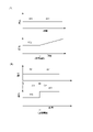
図5は、蒸着が進行する間の容器244の上部領域244a、中間領域244c、下部領域244bの温度分布を模式的に示している。図5(A)は中間リフレクタ241を備えた本実施形態の温度分布例、図5(B)は中間リフレクタ241を備えていない比較例の温度分布例である。図中、縦軸が容器の底部244dからの高さ、横軸が温度を示し、T1が蒸着材料の蒸発目安温度、T2が、蒸着材料が劣化する目安となる劣化目安温度を示している。
FIG. 5 schematically shows the temperature distribution of the
まず、図5(B)の比較例について説明する。温度分布曲線B1は、蒸発目安温度T1まで上昇した時点の温度分布である。図示例で、温度分布が、底部側が低温で開口部側が高温となる温度勾配となっている。このような温度分布となるのは、例えば、容器の底部にヒータが無く、また、図2の例では、底部に接触する支持部材245を通じて熱が逃げるからである。もっとも、温度分布は一つの例示であって、このような温度勾配に限定されるものではない。温度分布曲線B1は、蒸着材料242の上面が最大充填位置の高さh1にある状態であり、蒸着が開始する時点の温度分布を示している。蒸着材料242の蒸発は、蒸着材料242の上面位置より少し上の壁面からの輻射熱によって生じるので、蒸着材料の上面位置より少し上の温度が蒸発目安温度T1よりも高くなるように制御されている。この状態から蒸着が進行して蒸着材料242が減少していくと、蒸着材料242の高さが低くなり、蒸着材料242の上面が、温度が低い領域に移行していく。そこで、蒸着材料242の上面が位置する領域の温度が蒸発目安温度T1になるように、下部ヒータ246bに投入する電力を大きくし、低い領域の温度を高くなるように制御する。
First, the comparative example of FIG. 5B will be described. The temperature distribution curve B1 is the temperature distribution at the point when the temperature rises to the target evaporation temperature T1. In the illustrated example, the temperature distribution has a temperature gradient with a low temperature on the bottom side and a high temperature on the opening side. Such a temperature distribution is provided, for example, because there is no heater at the bottom of the container and, in the example of FIG. 2, heat escapes through the
温度分布曲線B2は、蒸着材料242の上面が高さh2まで低下した時点、温度分布曲線B3は、蒸着材料242の上面が高さh3まで低下した時点の温度分布である。温度分布曲線B2は温度分布曲線B1に対して、全体的に高くなり、図中左側にシフトした状態となる。さらに、温度分布曲線B3は、温度分布曲線B2に対してさらに、左側にシフトした状態に移行し、いずれも、上部領域244aの開口部244eの温度が上がりすぎて、劣化目安温度T2を超え、蒸着材料が劣化するおそれがある。蒸着材料が劣化すると、蒸着レート、成膜の品質を一定に保てなくなる。また、過熱した開口部244eからの輻射熱による基板10への熱影響も懸念される。
The temperature distribution curve B2 is the temperature distribution when the upper surface of the
鋭意検討した結果、この過熱の原因は、下部ヒータ246bの輻射熱が上部ヒータ246a側に及んでいることが一因であることが分かった。そこで、本発明は、上部ヒータ246aと下部ヒータ246bの間に中間リフレクタ241を配置し、下部ヒータ246bから上部ヒータ246a側に輻射される輻射熱を遮断し、下部ヒータ246bからの輻射熱の影響を抑えている。一方、上部領域244aは、下部ヒータ246bからの熱輻射が無くなり、上部ヒータ246aからの輻射熱のみとなって供給される熱エネルギが小さくなるので、中間リフレクタ241の上面241aで下部ヒータ246b側に向かう輻射熱を反射して上部領域244aを効率的に加熱している。
As a result of intensive investigation, it was found that one of the causes of this overheating is that radiant heat from the
次に、図5(A)を用いて、中間リフレクタ241を設けた場合の温度分布曲線について説明する。温度分布曲線A1は、蒸発開始の状態で、蒸着材料242の上面が高さh1(最大充填位置)にある。中間リフレクタ241を設けた中間領域244cにおいて、温
度が低下し、上部領域244aは、上部ヒータ246aからの輻射熱が中間リフレクタ241に反射されて効率的に加熱され、高温に維持されている。温度分布曲線A2は、蒸着材料242の上面が高さh2まで低下した時点、温度分布曲線A3は、蒸着材料242の上面が高さh3まで低下した時点の温度分布であり、下部領域244bについては、比較例と同様に、図中左側にシフトして、温度が上昇していく。しかし、上部領域244aについては、中間リフレクタ241によって下部ヒータ246bから上部ヒータ246a側への輻射熱が遮断されるので、温度分布は変化せず、蒸発目安温度T1よりも高く、かつ、劣化目安温度T2よりも低い温度に維持することができる。したがって、開口部244eに蒸着材料が付着することが防止され、かつ、一定の蒸着レートで、成膜の品質を一定に保つことができる。また、基板への熱影響を防止することができる。
Next, the temperature distribution curve when the
図6には、中間リフレクタ241による輻射熱の反射状態を模式的に示している。白抜き矢印は輻射熱の方向を概略的に示している。上部ヒータ246aからの輻射熱は対向する容器244の上部領域244aに輻射され、さらに上部リフレクタ248aによって、背面側に輻射される輻射熱も反射されて容器胴部の上部領域244aに輻射され、上部領域244aが加熱される。一方、下部ヒータ246b側へ向かう輻射熱については、容器胴部の中心軸と平行の軸方向の輻射熱(以下、軸方向輻射熱)をG1とし、中心軸線に対して直交する直交面に対して、容器に向けて所定角度下部ヒータ246b側に傾いた斜め方向の輻射熱(以下、斜め方向輻射熱)をG2とする。斜め方向の輻射熱G2は中間リフレクタ241の上面241aによって反射されて上部領域244aを加熱する。また、軸方向輻射熱G1については、中間リフレクタ241の上面241aによって反射された一部G11が、開口部244e付近に直接入射、あるいは上部リフレクタ248a側に向かう輻射熱G12が上部リフレクタ248aで再反射されて開口部244e付近に入射し、開口部244e付近を加熱する。
FIG. 6 schematically shows how radiant heat is reflected by the
開口部244e付近への反射効率を高めるために、例えば、図6(B)に示すように、斜め下向きの輻射熱の反射面241a1と、軸方向輻射熱G1の反射面241a2の傾きを変えて、軸方向輻射熱G1の反射面241a2を開口部側に傾けてもよい。また、図6(C)に示すように、反射面241a2を凹面形状とし、開口部側への反射量を大きくするようにしてもよい。また、図6(D)に示すように、斜め輻射熱の反射面241a1についても、傾けておけば、中間領域244cの加熱を促進することもできる。
In order to increase the efficiency of reflection to the vicinity of the
次に、下部ヒータ246bから上部ヒータ246a側に向かう輻射熱について説明すると、下部ヒータ246bからの輻射熱は対向する容器の下部領域244bに輻射され、さらに下部リフレクタ248bによって、背面側に輻射される輻射熱も反射されて下部領域244bに輻射される。一方、上部ヒータ246a側へ向かう輻射熱については、容器胴部の中心軸と平行の軸方向の輻射熱(以下、軸方向輻射熱)をF1とし、中心軸線に対して直交する直交面に対して、容器に向けて所定角度だけ上部ヒータ246a側に傾いた斜め方向の輻射熱(以下、斜め方向輻射熱)をF2とする。斜め方向の輻射熱F2は中間リフレクタ241の上面241aによって反射されて下部領域244bを加熱する。また、軸方向輻射熱F1については、中間リフレクタ241の下面241bによって反射された一部F11が、容器の下端部付近に直接入射、あるいは下部リフレクタ248b側に向かう輻射熱F12が下部リフレクタ248bで再反射されて下端部付近に入射して下端部付近を加熱し、温度が低い下端部を効率的に加熱することができる。この中間リフレクタ241の下面241bの構成についても、図6(B)から(D)と同様に、傾きを変えることにより、加熱効率を高めることができる。
Next, the radiant heat directed from the
<有機電子デバイスの製造方法の具体例>
本実施形態では、蒸発源装置を備える蒸着装置(成膜装置)を用いた有機電子デバイスの製造方法の一例を説明する。以下、有機電子デバイスの例として有機電子デバイスであ
る有機EL表示装置の構成及び製造方法を例示する。まず、製造する有機EL表示装置について説明する。図7(a)は有機EL表示装置60の全体図、図7(b)は1画素の断面構造を表している。本実施形態の成膜装置が備える蒸発源装置240としては、上記の各実施形態にいずれかに記載の装置を用いる。
<Specific example of method for producing organic electronic device>
In this embodiment, an example of a method for manufacturing an organic electronic device using a vapor deposition apparatus (film formation apparatus) including an evaporation source device will be described. Hereinafter, as an example of the organic electronic device, the configuration and manufacturing method of an organic EL display device, which is an organic electronic device, will be illustrated. First, the organic EL display device to be manufactured will be described. FIG. 7A shows an overall view of the organic
図7(A)に示すように、有機EL表示装置60の表示領域61には、発光素子を複数備える画素62がマトリクス状に複数配置されている。詳細は後で説明するが、発光素子のそれぞれは、一対の電極に挟まれた有機層を備えた構造を有している。なお、ここでいう画素とは、表示領域61において所望の色の表示を可能とする最小単位を指している。本図の有機EL表示装置の場合、互いに異なる発光を示す第1発光素子62R、第2発光素子62G、第3発光素子62Bの組合せにより画素62が構成されている。画素62は、赤色発光素子と緑色発光素子と青色発光素子の組合せで構成されることが多いが、黄色発光素子とシアン発光素子と白色発光素子の組み合わせでもよく、少なくとも1色以上であれば特に制限されるものではない。
As shown in FIG. 7A, in a
図7(B)は、図7(A)のA-B線における部分断面模式図である。画素62は、被蒸着体である基板63上に、第1電極(陽極)64と、正孔輸送層65と、発光層66R,66G,66Bのいずれかと、電子輸送層67と、第2電極(陰極)68と、を備える有機EL素子を有している。これらのうち、正孔輸送層65、発光層66R,66G,66B、電子輸送層67が有機層に当たる。また、本実施形態では、発光層66Rは赤色を発する有機EL層、発光層66Gは緑色を発する有機EL層、発光層66Bは青色を発する有機EL層である。発光層66R,66G,66Bは、それぞれ赤色、緑色、青色を発する発光素子(有機EL素子と記述する場合もある)に対応するパターンに形成されている。また、第1電極64は、発光素子ごとに分離して形成されている。正孔輸送層65と電子輸送層67と第2電極68は、複数の発光素子62R,62G,62Bと共通で形成されていてもよいし、発光素子毎に形成されていてもよい。なお、第1電極64と第2電極68とが異物によってショートするのを防ぐために、第1電極64間に絶縁層69が設けられている。さらに、有機EL層は水分や酸素によって劣化するため、水分や酸素から有機EL素子を保護するための保護層70が設けられている。
FIG. 7B is a schematic partial cross-sectional view taken along the line AB of FIG. 7A. The
次に、有機EL表示装置の製造方法の例について具体的に説明する。
まず、有機EL表示装置を駆動するための回路(不図示)および第1電極64が形成された基板63を準備する。
Next, an example of a method for manufacturing an organic EL display device will be specifically described.
First, a
第1電極64が形成された基板63の上にアクリル樹脂をスピンコートで形成し、アクリル樹脂をリソグラフィ法により、第1電極64が形成された部分に開口が形成されるようにパターニングし絶縁層69を形成する。この開口部が、発光素子が実際に発光する発光領域に相当する。
An acrylic resin is formed by spin coating on the
絶縁層69がパターニングされた基板63を第1の成膜装置に搬入し、基板保持ユニットにて基板を保持し、正孔輸送層65を、表示領域の第1電極64の上に共通する層として成膜する。正孔輸送層65は真空蒸着により成膜される。実際には正孔輸送層65は表示領域61よりも大きなサイズに形成されるため、高精細なマスクは不要である。ここで、本ステップでの成膜や、以下の各レイヤーの成膜において用いられる成膜装置は、上記各実施形態のいずれかに記載された蒸発源装置を備えている。蒸発源装置が上記実施形態の構成を持ち、上記実施形態に記載の加熱制御を行うことにより、容器の開口付近を高温に保ったまま、蒸着レートを一定に保つことができ、一定の膜厚の正孔輸送層65の成膜を行うことができる。
A
次に、正孔輸送層65までが形成された基板63を第2の成膜装置に搬入し、基板保持
ユニットにて保持する。基板とマスクとのアライメントを行い、基板をマスクの上に載置し、基板63の赤色を発する素子を配置する部分に、赤色を発する発光層66Rを成膜する。本例によれば、マスクと基板とを良好に重ね合わせることができ、高精度な成膜を行うことができる。
Next, the
発光層66Rの成膜と同様に、第3の成膜装置により緑色を発する発光層66Gを成膜し、さらに第4の成膜装置により青色を発する発光層66Bを成膜する。発光層66R、66G、66Bの成膜が完了した後、第5の成膜装置により表示領域61の全体に電子輸送層67を成膜する。電子輸送層67は、3色の発光層66R、66G、66Bに共通の層として形成される。
Similarly to the deposition of the
電子輸送層67までが形成された基板をスパッタリング装置に移動し、第2電極68を成膜し、その後プラズマCVD装置に移動して保護層70を成膜して、有機EL表示装置60が完成する。
The substrate on which the
絶縁層69がパターニングされた基板63を成膜装置に搬入してから保護層70の成膜が完了するまでは、水分や酸素を含む雰囲気にさらしてしまうと、有機EL材料からなる発光層が水分や酸素によって劣化してしまうおそれがある。従って、本例において、成膜装置間の基板の搬入搬出は、真空雰囲気または不活性ガス雰囲気の下で行われる。
If the
このようにして得られた有機EL表示装置は、発光素子ごとに発光層が精度よく形成される。従って、上記製造方法を用いれば、発光層の位置ずれに起因する有機EL表示装置の不良の発生を抑制することができる。本実施形態に係る成膜装置によれば、蒸発源装置の加熱を適切に制御することにより、良好な蒸着が可能となる。 In the organic EL display device thus obtained, the light-emitting layer is formed with high precision for each light-emitting element. Therefore, by using the manufacturing method described above, it is possible to suppress the occurrence of defects in the organic EL display device due to the misalignment of the light-emitting layer. According to the film forming apparatus according to this embodiment, by appropriately controlling the heating of the evaporation source device, good vapor deposition is possible.
240 蒸発源装置
241 中間リフレクタ(中間反射部材)
242 蒸着材料
244 容器
244a 上部領域(第1領域)
244b 下部領域(第2領域)
244e 開口部
246 ヒータ
246a 上部ヒータ(第1ヒータ)
246b 下部ヒータ(第2ヒータ)
270 制御部
240
242
244b lower region (second region)
246b lower heater (second heater)
270 control unit
Claims (13)
前記容器は、加熱された蒸着材料が放出される開口部と、第1領域と、前記第1領域よりも前記開口部から離れた領域である第2領域と、を有し、
前記第1領域を加熱する第1ヒータと、
前記第2領域を加熱する第2ヒータと、
前記第1ヒータと前記第2ヒータをそれぞれ独立に制御する制御部と、
前記第1ヒータと前記第2ヒータとの間に配置され、前記第1ヒータからの熱の少なくとも一部を反射する中間反射部材と、を有し、
前記制御部は、前記容器に収容された蒸着材料の減少に伴って、前記第2ヒータに投入する電力を上げることを特徴とする蒸発源装置。 An evaporation source device for heating a container containing an evaporation material to deposit the evaporation material on an object to be evaporated,
The container has an opening from which heated vapor deposition material is discharged, a first region, and a second region that is a region further from the opening than the first region,
a first heater that heats the first region;
a second heater that heats the second region;
a control unit that independently controls the first heater and the second heater;
an intermediate reflecting member disposed between the first heater and the second heater and reflecting at least part of heat from the first heater;
The evaporation source device, wherein the control unit increases power supplied to the second heater as the amount of the vapor deposition material contained in the container decreases.
前記容器は、加熱された前記蒸着材料が放出される開口部と、第1領域と、前記第1領域よりも前記開口部から離れた領域である第2領域と、を有し、
前記第1領域を加熱する第1ヒータと、
前記第2領域を加熱する第2ヒータと、
前記第1ヒータと前記第2ヒータをそれぞれ独立に制御する制御部と、
前記第1ヒータと前記第2ヒータとの間に配置され、前記第1ヒータからの熱の少なくとも一部を反射する中間反射部材と、を有し、
前記制御部は、
前記第1ヒータに第1の電力を投入しつつ、前記第2ヒータに第2の電力を投入する第1の加熱制御と、
前記第1の加熱制御を行った後に、前記第1ヒータに前記第1の電力を投入しつつ、前記第2ヒータに前記第2の電力よりも大きな第3の電力を投入する第2の加熱制御と、
を行うことを特徴とする蒸発源装置。 An evaporation source device for heating a container containing an evaporation material to deposit the evaporation material on an object to be evaporated,
The container has an opening from which the heated vapor deposition material is discharged, a first region, and a second region that is a region further from the opening than the first region,
a first heater that heats the first region;
a second heater that heats the second region;
a control unit that independently controls the first heater and the second heater;
an intermediate reflecting member disposed between the first heater and the second heater and reflecting at least part of heat from the first heater;
The control unit
a first heating control of applying a second electric power to the second heater while applying a first electric power to the first heater;
After performing the first heating control, a second heating in which the first electric power is applied to the first heater and a third electric power larger than the second electric power is applied to the second heater. control and
An evaporation source device characterized by performing
前記制御部は、前記温度検出手段の検出信号に基づいて、前記第1ヒータ近傍の温度を一定に保つように、前記第1ヒータの出力を調節する請求項4に記載の蒸発源装置。 Further comprising temperature detection means for detecting the temperature near the first heater,
5. The evaporation source device according to claim 4, wherein the control unit adjusts the output of the first heater based on the detection signal of the temperature detection means so as to keep the temperature in the vicinity of the first heater constant.
前記制御部は、前記レート検出手段からの信号に基づいて前記第2ヒータに投入する電力を調節する請求項1から5のいずれか1項に記載の蒸発源装置。 comprising rate detection means for detecting an evaporation rate of the vapor deposition material;
6. The evaporation source device according to any one of claims 1 to 5, wherein the control unit adjusts power supplied to the second heater based on a signal from the rate detection means.
前記制御部は、前記レート検出手段からの信号に基づいて取得した蒸発レートが予め設定された値以下で、前記温度検出手段で検出された温度が予め設定された値以上となった場合には、エラー信号を出力する請求項1から4のいずれか1項に記載の蒸発源装置。 having temperature detection means for detecting a temperature near the first heater and rate detection means for detecting an evaporation rate of the vapor deposition material;
When the evaporation rate obtained based on the signal from the rate detecting means is equal to or lower than a preset value and the temperature detected by the temperature detecting means is equal to or higher than a preset value, 5. The evaporation source device according to any one of claims 1 to 4, which outputs an error signal.
該蒸発源装置が配置され、被蒸着体に前記蒸着材料の蒸着が行われる真空チャンバと、を備えることを特徴とする成膜装置。 an evaporation source device according to any one of claims 1 to 9;
and a vacuum chamber in which the evaporation source device is arranged and the vapor deposition material is vapor-deposited on the object to be vapor-deposited.
前記容器は、加熱された前記蒸着材料が放出される開口部と、第1領域と、前記第1領域よりも前記開口部から離れた領域である第2領域と、を有し、
前記蒸発源装置は、前記第1領域を加熱する第1ヒータと、前記第2領域を加熱する第2ヒータと、前記第1ヒータと前記第2ヒータとの間に配置され前記第1ヒータからの熱の少なくとも一部を反射する中間反射部材と、を有し、
蒸発する蒸着材料の減少に応じて前記第2ヒータに投入する電力を上げて蒸発レートを制御することを特徴とする成膜方法。 A film formation method using an evaporation source device for heating a container containing an evaporation material to deposit the evaporation material on an object to be evaporated,
The container has an opening from which the heated vapor deposition material is discharged, a first region, and a second region that is a region further from the opening than the first region,
The evaporation source device includes a first heater that heats the first region, a second heater that heats the second region, and a heater disposed between the first heater and the second heater. an intermediate reflective member that reflects at least a portion of the heat of
A film formation method, wherein the evaporation rate is controlled by increasing the electric power supplied to the second heater according to the decrease of the vapor deposition material to evaporate.
前記容器は、加熱された前記蒸着材料が放出される開口部と、第1領域と、前記第1領域よりも前記開口部から離れた領域である第2領域と、を有し、
前記蒸発源装置は、前記第1領域を加熱する第1ヒータと、前記第2領域を加熱する第2ヒータと前記第1ヒータと前記第2ヒータとの間に配置され前記第1ヒータからの熱の少なくとも一部を反射する中間反射部材と、を有し、
前記第1ヒータに第1の電力を投入しつつ、前記第2ヒータに第2の電力を投入する第1の加熱制御と、
前記第1の加熱制御を行った後に、前記第1ヒータに前記第1の電力を投入しつつ、前記第2ヒータに前記第2の電力よりも大きな第3の電力を投入する第2の加熱制御と、
を行うことを特徴とする成膜方法。 A film formation method using an evaporation source device for heating a container containing an evaporation material to deposit the evaporation material on an object to be evaporated,
The container has an opening from which the heated vapor deposition material is discharged, a first region, and a second region that is a region further from the opening than the first region,
The evaporation source device includes a first heater that heats the first region, a second heater that heats the second region, and an evaporation source device disposed between the first heater and the second heater. an intermediate reflective member that reflects at least a portion of the heat;
a first heating control of applying a second electric power to the second heater while applying a first electric power to the first heater;
After performing the first heating control, a second heating in which the first electric power is applied to the first heater and a third electric power larger than the second electric power is applied to the second heater. control and
A film forming method characterized by performing
Priority Applications (3)
| Application Number | Priority Date | Filing Date | Title |
|---|---|---|---|
| JP2019099034A JP7202971B2 (en) | 2019-05-28 | 2019-05-28 | Evaporation Source Apparatus, Film Forming Apparatus, Film Forming Method, and Electronic Device Manufacturing Method |
| KR1020190168646A KR20200136801A (en) | 2019-05-28 | 2019-12-17 | Evaporation source apparatus, film formation apparatus, film formation method, and manufacturing method of electronic device |
| CN201911305385.1A CN112011761A (en) | 2019-05-28 | 2019-12-18 | Evaporation source apparatus, film forming method, and method for manufacturing electronic device |
Applications Claiming Priority (1)
| Application Number | Priority Date | Filing Date | Title |
|---|---|---|---|
| JP2019099034A JP7202971B2 (en) | 2019-05-28 | 2019-05-28 | Evaporation Source Apparatus, Film Forming Apparatus, Film Forming Method, and Electronic Device Manufacturing Method |
Publications (3)
| Publication Number | Publication Date |
|---|---|
| JP2020193360A JP2020193360A (en) | 2020-12-03 |
| JP2020193360A5 JP2020193360A5 (en) | 2022-03-10 |
| JP7202971B2 true JP7202971B2 (en) | 2023-01-12 |
Family
ID=73506948
Family Applications (1)
| Application Number | Title | Priority Date | Filing Date |
|---|---|---|---|
| JP2019099034A Active JP7202971B2 (en) | 2019-05-28 | 2019-05-28 | Evaporation Source Apparatus, Film Forming Apparatus, Film Forming Method, and Electronic Device Manufacturing Method |
Country Status (3)
| Country | Link |
|---|---|
| JP (1) | JP7202971B2 (en) |
| KR (1) | KR20200136801A (en) |
| CN (1) | CN112011761A (en) |
Citations (4)
| Publication number | Priority date | Publication date | Assignee | Title |
|---|---|---|---|---|
| JP2002124479A (en) | 2000-10-19 | 2002-04-26 | Hitachi Kokusai Electric Inc | Method of manufacturing substrate processor and semiconductor device |
| JP2008305735A (en) | 2007-06-11 | 2008-12-18 | Canon Inc | Method of manufacturing organic electroluminescent element and vapor deposition apparatus |
| JP2011162846A (en) | 2010-02-10 | 2011-08-25 | Mitsubishi Heavy Ind Ltd | Vacuum evaporation source |
| JP2019031705A (en) | 2017-08-07 | 2019-02-28 | キヤノントッキ株式会社 | Evaporation source device and its control method |
Family Cites Families (2)
| Publication number | Priority date | Publication date | Assignee | Title |
|---|---|---|---|---|
| JP2014070227A (en) * | 2012-09-27 | 2014-04-21 | Hitachi High-Technologies Corp | Filming apparatus, and temperature control method and device for evaporation source of the filming apparatus |
| CN206916210U (en) * | 2017-07-03 | 2018-01-23 | 京东方科技集团股份有限公司 | Crucible, evaporation source and evaporated device |
-
2019
- 2019-05-28 JP JP2019099034A patent/JP7202971B2/en active Active
- 2019-12-17 KR KR1020190168646A patent/KR20200136801A/en active Search and Examination
- 2019-12-18 CN CN201911305385.1A patent/CN112011761A/en active Pending
Patent Citations (4)
| Publication number | Priority date | Publication date | Assignee | Title |
|---|---|---|---|---|
| JP2002124479A (en) | 2000-10-19 | 2002-04-26 | Hitachi Kokusai Electric Inc | Method of manufacturing substrate processor and semiconductor device |
| JP2008305735A (en) | 2007-06-11 | 2008-12-18 | Canon Inc | Method of manufacturing organic electroluminescent element and vapor deposition apparatus |
| JP2011162846A (en) | 2010-02-10 | 2011-08-25 | Mitsubishi Heavy Ind Ltd | Vacuum evaporation source |
| JP2019031705A (en) | 2017-08-07 | 2019-02-28 | キヤノントッキ株式会社 | Evaporation source device and its control method |
Also Published As
| Publication number | Publication date |
|---|---|
| KR20200136801A (en) | 2020-12-08 |
| CN112011761A (en) | 2020-12-01 |
| JP2020193360A (en) | 2020-12-03 |
Similar Documents
| Publication | Publication Date | Title |
|---|---|---|
| KR101901072B1 (en) | Evaporation source device, film formation apparatus, film formation method and manufacturing method of electronic device | |
| KR102057783B1 (en) | Evaporator appratus and control method thereof | |
| WO2011034011A1 (en) | Vapor deposition method and vapor deposition apparatus | |
| KR102638573B1 (en) | Evaporation source device and vapor deposition apparatus | |
| CN110541146B (en) | Evaporation source device, evaporation device and evaporation system | |
| JP4478113B2 (en) | Heating vessel support and vapor deposition apparatus equipped with the same | |
| JP7241604B2 (en) | Heating device, evaporation source device, film forming device, film forming method, and electronic device manufacturing method | |
| JP7202971B2 (en) | Evaporation Source Apparatus, Film Forming Apparatus, Film Forming Method, and Electronic Device Manufacturing Method | |
| KR102617764B1 (en) | Film forming apparatus, film forming method and manufacturing method of electronic device | |
| JP7241603B2 (en) | Heating device, evaporation source device, film forming device, film forming method, and electronic device manufacturing method | |
| JP7162639B2 (en) | Evaporation source device, vapor deposition device, and control method for evaporation source device | |
| JP7088891B2 (en) | Evaporation source equipment and vapor deposition equipment | |
| US20100028534A1 (en) | Evaporation unit, evaporation method, controller for evaporation unit and the film forming apparatus | |
| JP2014065942A (en) | Vacuum evaporation device | |
| KR20140136650A (en) | Method for depositing a thin film | |
| JP6987822B2 (en) | Evaporation source device, film forming device, film forming method and manufacturing method of electronic device | |
| KR102150453B1 (en) | Evaporation source for deposition device |
Legal Events
| Date | Code | Title | Description |
|---|---|---|---|
| A521 | Request for written amendment filed |
Free format text: JAPANESE INTERMEDIATE CODE: A523 Effective date: 20220302 |
|
| A621 | Written request for application examination |
Free format text: JAPANESE INTERMEDIATE CODE: A621 Effective date: 20220302 |
|
| TRDD | Decision of grant or rejection written | ||
| A977 | Report on retrieval |
Free format text: JAPANESE INTERMEDIATE CODE: A971007 Effective date: 20221207 |
|
| A01 | Written decision to grant a patent or to grant a registration (utility model) |
Free format text: JAPANESE INTERMEDIATE CODE: A01 Effective date: 20221213 |
|
| A61 | First payment of annual fees (during grant procedure) |
Free format text: JAPANESE INTERMEDIATE CODE: A61 Effective date: 20221226 |
|
| R150 | Certificate of patent or registration of utility model |
Ref document number: 7202971 Country of ref document: JP Free format text: JAPANESE INTERMEDIATE CODE: R150 |