JP7202575B2 - ELECTRONIC DEVICE AND METHOD FOR MANUFACTURING ELECTRONIC DEVICE - Google Patents
ELECTRONIC DEVICE AND METHOD FOR MANUFACTURING ELECTRONIC DEVICE Download PDFInfo
- Publication number
- JP7202575B2 JP7202575B2 JP2020104857A JP2020104857A JP7202575B2 JP 7202575 B2 JP7202575 B2 JP 7202575B2 JP 2020104857 A JP2020104857 A JP 2020104857A JP 2020104857 A JP2020104857 A JP 2020104857A JP 7202575 B2 JP7202575 B2 JP 7202575B2
- Authority
- JP
- Japan
- Prior art keywords
- electronic device
- housing
- electrode
- cover
- surface resistivity
- Prior art date
- Legal status (The legal status is an assumption and is not a legal conclusion. Google has not performed a legal analysis and makes no representation as to the accuracy of the status listed.)
- Active
Links
Images


Classifications
-
- H—ELECTRICITY
- H05—ELECTRIC TECHNIQUES NOT OTHERWISE PROVIDED FOR
- H05F—STATIC ELECTRICITY; NATURALLY-OCCURRING ELECTRICITY
- H05F1/00—Preventing the formation of electrostatic charges
- H05F1/02—Preventing the formation of electrostatic charges by surface treatment
-
- H—ELECTRICITY
- H05—ELECTRIC TECHNIQUES NOT OTHERWISE PROVIDED FOR
- H05F—STATIC ELECTRICITY; NATURALLY-OCCURRING ELECTRICITY
- H05F3/00—Carrying-off electrostatic charges
- H05F3/04—Carrying-off electrostatic charges by means of spark gaps or other discharge devices
-
- H—ELECTRICITY
- H01—ELECTRIC ELEMENTS
- H01T—SPARK GAPS; OVERVOLTAGE ARRESTERS USING SPARK GAPS; SPARKING PLUGS; CORONA DEVICES; GENERATING IONS TO BE INTRODUCED INTO NON-ENCLOSED GASES
- H01T19/00—Devices providing for corona discharge
-
- H—ELECTRICITY
- H01—ELECTRIC ELEMENTS
- H01T—SPARK GAPS; OVERVOLTAGE ARRESTERS USING SPARK GAPS; SPARKING PLUGS; CORONA DEVICES; GENERATING IONS TO BE INTRODUCED INTO NON-ENCLOSED GASES
- H01T19/00—Devices providing for corona discharge
- H01T19/04—Devices providing for corona discharge having pointed electrodes
-
- H—ELECTRICITY
- H01—ELECTRIC ELEMENTS
- H01T—SPARK GAPS; OVERVOLTAGE ARRESTERS USING SPARK GAPS; SPARKING PLUGS; CORONA DEVICES; GENERATING IONS TO BE INTRODUCED INTO NON-ENCLOSED GASES
- H01T23/00—Apparatus for generating ions to be introduced into non-enclosed gases, e.g. into the atmosphere
-
- H—ELECTRICITY
- H05—ELECTRIC TECHNIQUES NOT OTHERWISE PROVIDED FOR
- H05F—STATIC ELECTRICITY; NATURALLY-OCCURRING ELECTRICITY
- H05F3/00—Carrying-off electrostatic charges
- H05F3/02—Carrying-off electrostatic charges by means of earthing connections
Landscapes
- Physics & Mathematics (AREA)
- Engineering & Computer Science (AREA)
- Plasma & Fusion (AREA)
- Elimination Of Static Electricity (AREA)
- Coating Of Shaped Articles Made Of Macromolecular Substances (AREA)
Description
本発明は、電子装置、及び電子装置の製造方法に関する。 The present invention relates to an electronic device and a method of manufacturing an electronic device.
これまで電子部品・電子機器やその製造工程における静電気対策について様々な開発がなされてきた。この種の技術として、例えば、特許文献1に記載の技術が知られている。特許文献1には、コロナ放電を生じてイオンを発生する放電針を備えるイオナイザが記載されている(特許文献1の請求項1等)。 So far, various developments have been made on countermeasures against static electricity in electronic parts, electronic equipment, and their manufacturing processes. As this type of technology, for example, the technology described in Patent Document 1 is known. Patent Document 1 describes an ionizer provided with a discharge needle that generates ions by generating corona discharge (Claim 1 of Patent Document 1, etc.).
しかしながら、本発明者が検討した結果、上記特許文献1に記載のイオナイザ等の電子装置において、その使用時に近傍に存在する電子部品・電子機器等の除電対象物における誘導帯電現象の緩和の点で改善の余地があることが判明した。 However, as a result of examination by the present inventors, in the electronic device such as the ionizer described in Patent Document 1, the induction charging phenomenon in an object to be neutralized, such as an electronic component or an electronic device, which exists in the vicinity of the device during use, has been found to be alleviated. It turned out that there was room for improvement.
本発明者はさらに検討したところ、電子部品、筐体を備え、高圧電源で駆動する電子装置について、電気部品を覆うカバー部及び/又は筐体の表面抵抗率を適切に制御することにより、電子装置の使用時において、その近傍に存在する除電対象物に発生する誘導帯電現象を緩和できることを見出し、本発明を完成するに至った。 As a result of further studies by the present inventors, it has been found that an electronic device comprising electronic components and a housing and driven by a high-voltage power supply can be electronically The present inventors have found that the induction charging phenomenon occurring in the object to be neutralized in the vicinity thereof during use of the device can be alleviated, and have completed the present invention.
本発明によれば、
除電対象物の近傍で使用される電子装置であって、
電気部品と、
前記電気部品に高圧電源の電力を送電する配線部と、
前記電気部品及び前記配線部を収容する筐体と、を備え、
前記電気部品の少なくとも一部を覆うカバー部を備え、前記カバー部の表面抵抗率が104Ω/□以上1011Ω/□以下となる構成、及び、前記筐体の表面抵抗率が104Ω/□以上1011Ω/□以下となる構成の少なくとも一方の構成を有する、電子装置が提供される。
According to the invention,
An electronic device used in the vicinity of an object to be statically removed,
electrical components;
a wiring unit for transmitting power from a high-voltage power supply to the electrical component;
A housing that accommodates the electrical component and the wiring unit,
A cover portion covering at least a portion of the electric component is provided, and the cover portion has a surface resistivity of 10 4 Ω/□ or more and 10 11 Ω/□ or less, and the housing has a surface resistivity of 10 4 . Provided is an electronic device having at least one configuration of Ω/□ or more and 10 11 Ω/□ or less.
また本発明によれば、
電気部品と、前記電気部品に高圧電源の電力を送電する配線部と、前記電気部品及び前記配線部を収容する筐体と、を備え、除電対象物の近傍で使用される電子装置の製造方法であって、
表面抵抗率が104Ω/□以上1011Ω/□以下であり、前記電気部品の少なくとも一部を覆うカバー部、及び表面抵抗率が104Ω/□以上1011Ω/□以下である前記筐体の少なくとも一方を用いて、電子装置の構成部品を組み立てることにより前記電子装置を得る、組立工程を含む、電子装置の製造方法が提供される。
Also according to the present invention,
A method for manufacturing an electronic device used near an object to be neutralized, comprising an electric component, a wiring section for transmitting power of a high-voltage power supply to the electric component, and a housing for housing the electric component and the wiring section. and
The surface resistivity is 10 4 Ω/□ or more and 10 11 Ω/□ or less, and the surface resistivity of the cover portion that covers at least part of the electrical component is 10 4 Ω/□ or more and 10 11 Ω/□ or less. A method of manufacturing an electronic device is provided, including an assembly step of obtaining the electronic device by assembling components of the electronic device using at least one of the housings.
本発明によれば、誘導帯電現象の緩和に優れた電子装置、及び電子装置の製造方法が提供される。 ADVANTAGE OF THE INVENTION According to this invention, the manufacturing method of the electronic device excellent in alleviation of an induction charging phenomenon, and an electronic device is provided.
以下、本発明の実施の形態について、図面を用いて説明する。なお、すべての図面において、同様な構成要素には同様の符号を付し、適宜説明を省略する。また、図は概略図であり、実際の寸法比率とは一致していない。
なお、本実施の形態では図示するように前後左右上下の方向を規定して説明する。しかし、これは構成要素の相対関係を簡単に説明するために便宜的に規定するものである。したがって、本発明を実施する製品の製造時や使用時の方向を限定するものではない。
BEST MODE FOR CARRYING OUT THE INVENTION Hereinafter, embodiments of the present invention will be described with reference to the drawings. In addition, in all the drawings, the same constituent elements are denoted by the same reference numerals, and the description thereof will be omitted as appropriate. Also, the drawings are schematic diagrams and do not correspond to actual dimensional ratios.
In this embodiment, the front, back, left, right, up, and down directions are specified as shown in the drawings. However, this is defined for convenience in order to simply explain the relative relationship of the constituent elements. Therefore, it does not limit the orientation during manufacture or use of the product embodying the present invention.
本実施形態の電子装置について概説する。 An electronic device according to the present embodiment will be outlined.
本実施形態の電子装置は、電気部品と、電気部品に高圧電源の電力を送電する配線部と、電気部品及び配線部を収容する筐体と、を備え、電気部品の少なくとも一部を覆うカバー部を備え、そのカバー部の表面抵抗率が104Ω/□以上1011Ω/□以下となる構成、及び、筐体の表面抵抗率が104Ω/□以上1011Ω/□以下となる構成の少なくとも一方の構成を有する。
このような電子装置は、電子部品・電子機器等の除電対象物の近傍において使用される。
The electronic device of the present embodiment includes an electrical component, a wiring section for transmitting power from a high-voltage power supply to the electrical component, and a housing that houses the electrical component and the wiring section, and a cover that covers at least part of the electrical component. and the cover has a surface resistivity of 10 4 Ω/□ or more and 10 11 Ω/□ or less, and the housing has a surface resistivity of 10 4 Ω/□ or more and 10 11 Ω/□ or less. It has at least one configuration of the configuration.
Such an electronic device is used in the vicinity of an object to be neutralized, such as an electronic component or an electronic device.
電子部品・電子機器の製造・組立工程においては、静電気放電(ESD:Electro Static Discharge)による製品へのダメージを抑制することを目的として、各種の静電気対策が採用されている。 2. Description of the Related Art In manufacturing and assembling processes of electronic components and electronic equipment, various anti-static measures are adopted for the purpose of suppressing damage to products due to electrostatic discharge (ESD).
静電気対策の一つとして、除電装置(イオナイザ)を使用することが幅広く行われている。除電装置は、電子部品・電子機器における帯電電荷を中和することによって、ESDの発生を抑制できる。除電装置が採用される理由として、安全性が比較的高い事、設置場所への制約が少ない事、扱いやすい事等が挙げられる。 As one of countermeasures against static electricity, the use of a static eliminator (ionizer) is widely practiced. A static eliminator can suppress the occurrence of ESD by neutralizing the charge in electronic components and electronic equipment. Reasons for adopting static eliminators include relatively high safety, few restrictions on installation locations, and ease of handling.
近年、電子部品・電子機器の微細化や高速化、低動作電圧化、高機能化等に伴い、静電気放電(ESD)への耐久性が低下する恐れがあるため、静電気管理電圧を、数ボルト(V)~十数(V)程度の非常に低い値とすることが要求されてきている。例えば、静電気放電への感受性が非常に高いハードディスクドライブの磁気ヘッド・スライダー工程、CMOSイメージセンサー、SAWデバイス、高周波デバイス、SiC技術を採用したインバーター、レーザーダイオード、白色LED、高輝度LED等において、このような課題が顕著である。 In recent years, as electronic components and devices have become smaller, faster, have lower operating voltages, and have become more functional, there is a risk that their resistance to electrostatic discharge (ESD) will decrease. (V) to a very low value of about ten and several (V) is required. For example, in the magnetic head slider process of hard disk drives, CMOS image sensors, SAW devices, high-frequency devices, SiC technology inverters, laser diodes, white LEDs, high-brightness LEDs, etc., which are extremely sensitive to electrostatic discharge. Such issues are conspicuous.
このような背景を踏まえ、本発明者らが検討した結果、静電気管理電圧が低く設定される電子部品・電子機器の製造工程において、除電装置が除電対象物の帯電電荷を中和するとき、その高圧電源等に起因した電界によって、除電対象物にイオンが流入せずとも電位が誘導されることにより、静電気障害を引き起こす恐れがあることが判明した。 Based on this background, the inventors of the present invention have investigated, and found that in the manufacturing process of electronic components and electronic devices in which the static electricity management voltage is set low, when the static eliminator neutralizes the static charge of the static elimination object, It has been found that an electric field caused by a high-voltage power supply or the like induces a potential even if ions do not flow into the object to be statically eliminated, which may cause electrostatic failure.
これまでの除電装置の開発において、除電装置自体に静電気対策が施されてはいなかった。なぜならば、これまでは静電気管理電圧が比較的高い基準が設けられていたため、除電装置による除電対象物に生じる誘導帯電ついて着眼、検討されていなかったためである。すなわち、除電装置による誘導帯電について検討事項から除外したとしても、除電速度やイオンバランスなどの除電性能を高めれば、静電気対策として有効な除電装置を提供できていた。
しかしながら、今回、数ボルト(V)~十数(V)程度の静電気管理電圧が比較的低い基準が設定された。この場合、除電装置による除電対象物に生じる誘導帯電量は、無視できるレベルの静電気量ではなく、静電気対策の対象とすることがESDの発生抑制に有効でることが、本発明者の知見によって明らかとなった。
In the development of static eliminators so far, the static eliminator itself has not been subjected to static electricity countermeasures. This is because, up until now, relatively high standards have been set for the static electricity management voltage, and therefore, no consideration has been given to the induced electrification that occurs on an object to be statically eliminated by the static eliminator. That is, even if the induction charging by the static eliminator is excluded from consideration, the static eliminator can be provided as an effective countermeasure against static electricity by improving the static elimination performance such as the static elimination speed and the ion balance.
However, this time, a relatively low standard was set for static control voltages on the order of a few volts (V) to over a dozen (V). In this case, it is clear from the knowledge of the present inventor that the amount of induced charge generated on the object to be statically eliminated by the static eliminator is not a static amount at a negligible level, and that it is effective to suppress the occurrence of ESD by taking measures against static electricity. became.
さらに鋭意検討したところ、除電装置の筐体の表面抵抗率及び/又は電気部品を覆うカバー部の表面抵抗率を適切に制御することにより、除電装置の使用時において、その近傍に存在する除電対象物に発生する誘導帯電現象を緩和できることが見出された。 As a result of further intensive studies, it was found that by appropriately controlling the surface resistivity of the housing of the static eliminator and/or the surface resistivity of the cover portion that covers the electrical parts, when the static eliminator is in use, the object to be statically eliminated that exists in the vicinity It was found that the induction charging phenomenon that occurs in objects can be alleviated.
本実施形態によれば、除電対象物の近傍において、除電装置等の電子装置を使用するによって、静電誘導により除電対象物に発生する誘導電圧を低減させること、すなわち、誘導帯電現象の緩和が可能になる。
これにより、電子部品・電子機器の製造工程において、歩留まりを向上させること、品質のバラツキを低減させること等が期待できる。
また、本実施形態によれば、数ボルト(V)~十数(V)程度の静電気管理電圧が比較的低い基準においても、ESDの発生を抑制できる除電装置等の電子装置を提供できる。
According to the present embodiment, by using an electronic device such as a static eliminator in the vicinity of the static elimination target, the induced voltage generated in the static elimination target due to electrostatic induction can be reduced, that is, the induction charging phenomenon can be alleviated. be possible.
As a result, in the manufacturing process of electronic components and electronic equipment, it can be expected that the yield will be improved and the variation in quality will be reduced.
Further, according to this embodiment, it is possible to provide an electronic device such as a static eliminator capable of suppressing the occurrence of ESD even with a relatively low static electricity control voltage of several volts (V) to several tens of volts (V).
以下、本実施形態の電子装置について詳述する。 The electronic device of this embodiment will be described in detail below.
電子装置は、例えば、コロナ放電型除電装置(イオナイザ)、光照射型除電装置等が用いられる。コロナ放電型除電装置は、コロナ放電を発生させる放電針(電極)を備えるもので、電圧印加方式や自己放電方式がある。光照射型除電装置は、放射線の種類に応じて、紫外線方式、軟エックス線方式、若しくはα線方式がある。 As the electronic device, for example, a corona discharge type static eliminator (ionizer), a light irradiation type static eliminator, or the like is used. A corona discharge static eliminator has a discharge needle (electrode) that generates a corona discharge, and includes a voltage application method and a self-discharge method. Light irradiation type static eliminators are available in an ultraviolet system, a soft X-ray system, or an α-ray system, depending on the type of radiation.
なお、電子装置は、電子部品・電子機器やその製造工程において、除電対象物の近傍で使用されるものであれば、除電装置以外の一般的な電子装置であってもよい。
近傍とは、除電装置においては、除電処理を施すときの除電対象物と除電装置との距離にあることを意味してもよいが、同じ室内、同じ作業台、製造ライン上にあることでもよい。
Note that the electronic device may be a general electronic device other than the static eliminator as long as it is used in the vicinity of the object to be statically eliminated in the electronic component/electronic device or its manufacturing process.
In the case of a static eliminator, the term "nearby" may mean that there is a distance between the object to be statically eliminated and the static eliminator, but it may also be in the same room, on the same workbench, or on the production line. .
除電装置は、設置タイプでも、ハンディータイプでもよい。除電装置の型式は、例えば、バー型、オーバーヘッドコンソール型、デスクトップ型(ブロア型・ファン型)、ノズル型(スポット型)、ガン型、ペン型、ボックス型等が用いられる。 The static eliminator may be either an installation type or a handy type. The type of static eliminator is, for example, a bar type, an overhead console type, a desktop type (blower type/fan type), a nozzle type (spot type), a gun type, a pen type, a box type, or the like.
除電装置の印可電圧方式は、例えば、DC(直流)方式、パルスDC方式、SSDC方式、AC(交流)方式、高周波AC方式、パルスAC方式、HDC-AC方式などが挙げられる。 The applied voltage method of the static eliminator includes, for example, a DC (direct current) method, a pulse DC method, an SSDC method, an AC (alternating current) method, a high frequency AC method, a pulse AC method, and an HDC-AC method.
高圧電源の電圧は、例えば、100V以上でもよく、好ましくは1kV以上でもよく、2kV以上でもよい。高圧電源の電圧の上限は、特に限定されない。高圧電源は、必要に応じて、公知の各種変換回路を有してもよい。
なお、除電装置において、電気部品の一つである電極に印可される出力電圧は、好ましくは1kV以上でもよく、より好ましくは2kV以上である。
The voltage of the high-voltage power supply may be, for example, 100 V or higher, preferably 1 kV or higher, or 2 kV or higher. The upper limit of the voltage of the high voltage power supply is not particularly limited. The high-voltage power supply may have various known conversion circuits as required.
In the static eliminator, the output voltage applied to the electrode, which is one of the electrical components, may preferably be 1 kV or higher, more preferably 2 kV or higher.
高圧電源の周波数は、例えば、商用周波数型の50Hzや60Hz等、低周波型の数Hz~30Hz、高周波型の約20kHz~80kHz等を用いてもよい。 The frequency of the high-voltage power supply may be, for example, a commercial frequency type of 50 Hz or 60 Hz, a low frequency type of several Hz to 30 Hz, or a high frequency type of about 20 kHz to 80 kHz.
高圧電源は、内蔵電源でも、外部電源でもよい。内蔵電源は、例えば、電子部品を収容する筐体の内部に設置される。外部電源は、例えば、電子装置が使用される施設に敷設された電源やバッテリー等が用いられる。 The high voltage power supply may be an internal power supply or an external power supply. The built-in power supply is installed, for example, inside a housing that accommodates electronic components. As the external power supply, for example, a power supply, a battery, or the like installed in a facility where the electronic device is used is used.
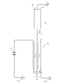
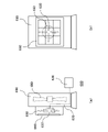
本実施形態の電子装置について、コロナ放電を発生させる除電装置の一つである、バー型のイオナイザ100を用いた一例について、図4、5を用いて説明する。
図4は、イオナイザ100の構造を模式的に示す断面図である。
図5は、図4中のα領域の拡大図を示す図である。
An example of an electronic device according to the present embodiment using a bar-
FIG. 4 is a cross-sectional view schematically showing the structure of the
FIG. 5 is a diagram showing an enlarged view of the α region in FIG.
図5のイオナイザ100は、一または二以上の電極130(電気部品)と、電極130に高圧電源120の電力を送電する配線部170と、電極130及び配線部170を収容する筐体110と、を備える。
収容とは、筐体110の内部空間の内部に、収容物の一部または全体が含まれた状態を意味する。
The
“Contained” means a state in which a part or the whole of the contained object is contained inside the internal space of the
電極130は、コロナ放電を発生させる電極、又はグロー放電を発生させる電極のいずれかが用いられており、先端が徐々に縮径する針状の金属棒、すなわち、放電針で構成される。
The
電極130の構成材料は、タングステン、ステンレス、シリコン、及び、ガラス等が用いられる。
タングステン製、ステンレス製等の金属製放電針、シリコン製(ポリシリコン製)の非金属製放電針は、それぞれの構成材料を高純度に含むように構成され得るが、必要に応じて他の材料が僅かに含まれることを許容する。ガラス製の放電針は、表面にシリコンコートが施されたものを使用できる。
As a constituent material of the
Metallic discharge needles made of tungsten, stainless steel, etc., and non-metallic discharge needles made of silicon (made of polysilicon) can be configured to contain their constituent materials with high purity, but other materials may be used as necessary. allow a small amount of A glass-made discharge needle having a surface coated with silicon can be used.
電極130の個数、電極130のピッチ間隔、複数の電極130が設置されるラインの長さ(電極長さ)等については、設置場所や除電能等を考慮して、設定可能である。
The number of
電極130に高圧電源120から電力が配線部170を介して送電されると、電極130からイオン140が放出される。放出されたイオン140によって、除電対象物Wの表面における帯電を中和(除電処理)できる。
When power is transmitted from the high-
イオナイザ100の電圧印加方式は、上述の方式から選択でき、特に限定されないが、例えば、AC(交流)方式、高周波AC方式、パルスAC方式、HDC-AC方式等の交流方式を用いてもよい。
交流方式の場合、交流の高圧電源120を用いてもよく、又は、直流の高圧電源120に交流発生回路を組み合わせたものを用いてもよい。
The voltage application method of the
In the case of an AC system, an AC high
図4のイオナイザ100が備える高圧電源120は、筐体110中に収容された内蔵電源であるが、この態様に限定されない。本実施形態によれば、高圧電源120が筐体110に内蔵された場合でも、除電対象物に発生する誘導帯電現象を緩和できる。
The high-
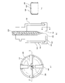
図4のイオナイザ100は、電極130の少なくとも一部を覆うカバー部(ノズル部150、ガード部160)を備える。
The
イオナイザ100中、カバー部が、筒状のノズル部150及び/又はガード部160で構成されてもよい。筒状のノズル部150の一例は、筐体110に設けられており、電極130の周囲を覆うように構成されてもよい。ガード部160の一例は、筒状のノズル部150に着脱自在に装着されており、電極130の少なくとも先端132を覆うように構成されてもよい。
In the
図5は、図4のα領域を拡大した図であり、カバー部に設置された電極130を模式的に示す図である。図5(a)は、電極130の軸心方向を先端132側から見た図、図5(b)は、図5(a)のA-A断面視における図、図5(c)は、図5(b)のB-B断面視における図である。
FIG. 5 is an enlarged view of the α region of FIG. 4 and schematically shows the
図5(b)中、カバー部は、電極130の先端132の周囲を覆うカバー構造(ノズル部150)、及び電極130の先端132の前方を覆うカバー構造(ガード部160)を有している。
バー型のイオナイザ100は、ノズル部150のみ有してもよいが、ノズル部150及びガード部160の両者を有する態様が好ましい。
In FIG. 5B, the cover part has a cover structure (nozzle part 150) that covers the periphery of the
The bar-
ノズル部150は、電極130の後方の一部を支持するソケット構造を有していて、筐体110の取付孔に着脱自在に装着される。電極130が損耗したとき、新しい電極130を有するノズル部150に交換することが可能となるため、メンテナンスが容易になる。着脱方法は、機械的結合などの公知の方法が使用できる。
なお、ノズル部150と筐体110は別部材で構成されてもよいが、両部材が一体化してなる一体部材で構成されてもよい。
The
In addition, the
ノズル部150は、電極130の軸芯方向における周囲を覆う壁部に一または二以上の穴部190を有してもよい。穴部190を介してエアを供給することが可能となり、電極130の除電特性を調整することが可能になる。エアは、筐体110中のコンプレッサから供給されるように構成されてもよい。
The
ノズル部150は、軸芯方向に対して周方向における電極130の表面の少なくとも一部を覆うカバー構造を有し、さらにソケット構造から突出した電極130の部分からその先端132までの周方向の表面全体を覆うような筒状のカバー構造を有してもよい。
The
また、ガード部160は、電極130の先端132前方に存在するノズル部150の開口134を覆うようなカバー構造を有する。このようなガード部160は、図5(a)に示す開口134内にある電極130の先端132が誤って操作者に触れてしまうことを防止できるため、フィンガーガードとして機能する。
Also, the
ガード部160は、ノズル部150に着脱自在に装着される。ガード部160のみを交換可能となる。着脱方法は、機械的結合などの公知の方法が使用できる。
なお、ガード部160とノズル部150は別部材で構成されてもよいが、一体部材で構成されてもよい。
The
The
本実施形態のイオナイザ100において、電極130(電気部品)の少なくとも一部を覆うカバー部(ノズル部150、及び/又はガード部160)を備え、カバー部の表面抵抗率が104Ω/□以上1011Ω/□以下となる構成A、及び、筐体110の表面抵抗率が104Ω/□以上1011Ω/□以下となる構成の少なくとも一方の構成Bを有する。
構成A及び構成Bの表面抵抗率は、それぞれ同一でも異なってもよい。
イオナイザ100は、構成Aのみ、又は構成Bのみを有してもよいが、好ましくは構成Aおよび構成Bの両方を有する。
The
The surface resistivities of Configuration A and Configuration B may each be the same or different.
The
構成A:カバー部の表面抵抗率は、1.0×10⁴Ω/□以上1.0×1011Ω/□以下、好ましくは1.0×104Ω/□以上1.0×1010Ω/□以下、より好ましくは1.0×104Ω/□以上1.0×109Ω/□以下、さらに好ましくは1.0×105Ω/□以上1.0×109Ω/□以下である。 Structure A: The surface resistivity of the cover part is 1.0×10 4 Ω/□ or more and 1.0×10 11 Ω/□ or less, preferably 1.0×10 4 Ω/□ or more and 1.0×10 10 Ω/□ or less, more preferably 1.0×10 4 Ω/□ or more and 1.0×10 9 Ω/□ or less, still more preferably 1.0×10 5 Ω/□ or more and 1.0×10 9 Ω/ □ is less than or equal to.
構成B:筐体110の表面抵抗率は、それぞれ同一でも異なってもよく、1.0×10⁴Ω/□以上1.0×1011Ω/□以下、好ましくは1.0×104Ω/□以上1.0×1010Ω/□以下、より好ましくは1.0×104Ω/□以上1.0×109Ω/□以下、さらに好ましくは1.0×105Ω/□以上1.0×109Ω/□以下である。
Configuration B: The surface resistivity of the
本明細書において、表面抵抗率とは、例えば、温度:22.5℃±10%、湿度:50%RH±5℃の環境下で、IEC 61340 5-1,5-2規格で定義された(ESD Association standardsに順応した)表面抵抗計を使用し、CRプローブ或いは2Pプローブを用いて測定した値(Ω/□)を採用できる。 In this specification, the surface resistivity is, for example, temperature: 22.5 ° C. ± 10%, humidity: 50% RH ± 5 ° C., IEC 61340 5-1, 5-2 standards defined A value (Ω/□) measured using a CR probe or 2P probe using a surface resistance meter (compliant with ESD Association standards) can be adopted.
上記の構成A及び構成Bの少なくとも一方を備えることによって、イオナイザ100から発生する電界が、除電対象物Wに引き起こす誘導帯電現象を緩和できる。
By providing at least one of the configuration A and the configuration B described above, the induction charging phenomenon caused in the static elimination object W by the electric field generated from the
詳細なメカニズムは定かではないが、上記の表面抵抗率を有するカバー部や筐体によって、絶縁性材料と比較して電荷の移動がスムーズになる一方で、導電性材料と比較して電極130から発生するイオンの引きつけ量の増大を抑制できるため、除電時において除電対象物Wに生じる誘導電圧を低減できる一方で、イオナイザ100の除電性能の低下を抑制できる、と考えられる。
Although the detailed mechanism is not clear, the cover portion and housing having the above-described surface resistivity allow the charge to move more smoothly than the insulating material, while the
筐体110の表面抵抗率をAとし、カバー部の表面抵抗率をBとしたとき、AおよびBが、例えば、103/1012≦A/B<1、好ましくは104/1011≦A/B<1、より好ましくは104/109≦A/B<1を満たすようにイオナイザ100が構成されてもよい。これにより、カバー部による除電能の低下を抑制しつつも、カバー部から筐体110に電荷の移動をスムーズに行う事が可能になる。
なお、他の態様として、AおよびBが、例えば、1<A/B≦103/1012を満たすようにイオナイザ100が構成されてもよい。
When A is the surface resistivity of the
As another aspect, the
イオナイザ100において、筐体110およびカバー部(ノズル部150、ガード部160)の少なくとも一方が、絶縁性の層又は導電性の層と、その層の表面の少なくとも一部に形成された、表面抵抗率が104Ω/□以上1011Ω/□以下の静電気拡散性層180と、を有するように構成されてもよい。
In the
ここで、イオナイザの技術分野において、放電針が設置されたノズルや、ノズルのフィンガーガードには、通常、絶縁性材料を使用し、導電性材料を使用しないことが一般的に行われている。これは、導電性材料が、放電針から放出されたイオンを引きつけてしまうため、イオナイザの除電能を低下させ、その結果、除電対象物Wが十分に除電されない恐れがあるためであった。しかしながら、通常の絶縁性材料を使用すると、上述の通り、除電対象物Wに生じる誘導電圧が高くなり、ESDが発生する恐れがあった。 Here, in the technical field of ionizers, it is common practice to use an insulating material and not a conductive material for a nozzle having a discharge needle and a finger guard for the nozzle. This is because the conductive material attracts the ions emitted from the discharge needle, which may reduce the static elimination performance of the ionizer, and as a result, the static elimination object W may not be sufficiently static eliminated. However, when a normal insulating material is used, as described above, the induced voltage generated in the static elimination object W increases, and there is a risk of ESD occurring.
これに対して、絶縁性層の上に静電気拡散性層を積層する第一積層構造、あるいは、導電性層の上に静電気拡散性層を積層する第二積層構造のいずれか一方を採用することによって、イオナイザの除電能の低下を抑制しつつも、除電時において除電対象物Wに生じる誘導電圧を低減させることが可能になる。 On the other hand, either the first laminated structure in which the static electricity dissipative layer is laminated on the insulating layer or the second laminated structure in which the static electricity dissipative layer is laminated on the conductive layer is adopted. Thus, it is possible to reduce the induced voltage generated in the static elimination target W during static elimination while suppressing the deterioration of the static elimination performance of the ionizer.
このような積層構造は、電極130の軸芯方向における周囲を覆うノズル部150、電極130の先端132と除電対象物Wとの間に存在するガード部160、及び電極130を設置する筐体110のうち、少なくとも1以上に形成されることで、除電対象物Wに生じる誘導帯電現象を緩和できる。
この中でも、電極130のから生じたイオンの進行方向を妨げる位置に設置されるガード部160に積層構造が形成されることが好ましい。これにより、誘導電圧をより低減させることができる。また、より好ましくはガード部160及びノズル部150、さらに好ましくはノズル部150、ガード部160及び筐体110に積層構造が形成される。ガード部160が接触する部材や、その部材とさらに接触する別部材においても、上記の積層構造を形成することによって、より一層、除電対象物Wに生じる誘導電圧を低減できる。詳細なメカニズムは定かではないが、電極130から生じたイオンの移動が、ガード部160を介してスムーズに行われるため、除電時において除電対象物Wに生じる誘導電圧を低減できると考えられる。
Such a laminated structure includes a
Among these, it is preferable that the
積層構造中の静電気拡散性層180の表面抵抗率の測定は、単独ではなく、下地層である絶縁性層または導電性層に積層した状態で測定されるものである。例えば、導電性層の下地層を用いることで、表面抵抗率の値を、単独の場合よりも小さく調整することが可能である。
The surface resistivity of the static
第一積層構造中の絶縁性層には、例えば、ABS、PC、PE、PP、PMMA、PS、PVC、POM、その他のエラストマー樹脂やエンプラ樹脂、これらの樹脂を2種以上含むポリマーアロイ樹脂などの熱可塑性樹脂を用いることができる。熱可塑性樹脂は、金属材料と比べて軽量で、成形性に優れ、所望の部材形状が得られる。 The insulating layer in the first laminated structure includes, for example, ABS, PC, PE, PP, PMMA, PS, PVC, POM, other elastomer resins, engineering plastic resins, polymer alloy resins containing two or more of these resins, and the like. of thermoplastic resin can be used. Thermoplastic resins are lighter than metal materials, have excellent moldability, and can be formed into desired member shapes.
また、第二積層構造中の導電性層には、SUS、SPCC、S〇〇C等の合金鋼等の鉄鋼材、Al合金、Cu合金等の合金材等の金属材料を用いてもよく、カーボンやAg等の導電材を上記の熱硬化性樹脂等の樹脂に練り込んだ導電性樹脂などを用いることが可能である。 In addition, for the conductive layer in the second laminated structure, metal materials such as steel materials such as alloy steels such as SUS, SPCC, and SOOC, and alloy materials such as Al alloys and Cu alloys may be used. It is possible to use a conductive resin obtained by kneading a conductive material such as carbon or Ag into a resin such as the above thermosetting resin.
詳細なメカニズムは定かではないが、第一積層構造では、下地の表面に形成された静電気拡散性層中を通って電荷が移動するのに対し、第二積層構造では、静電気拡散性層中のみならず、静電気拡散性層から下地の導電性層に移動した電荷が、その導電性層中も移動することが可能にあるため、より効率的に誘導帯電現象を緩和できる、と考えられる。 Although the detailed mechanism is not clear, in the first laminated structure, the charge moves through the static electricity dissipative layer formed on the surface of the base, whereas in the second laminated structure, only in the static electricity dissipative layer Rather, it is considered that the charge that has migrated from the static electricity diffusion layer to the underlying conductive layer can also migrate in the conductive layer, so that the induction charging phenomenon can be more efficiently mitigated.
静電気拡散性層を、絶縁性層または導電性層上に形成する方法としては、例えば、塗料を用いて塗膜を成膜する方法、薄膜フィルムを積層する方法、成形材料を用いて成形する方法等が挙げられる。静電気拡散性層を単独で形成してよいが、2色成形などの手法を用いることで、絶縁性層または導電性層の下地層と静電気拡散性層とを同時に形成することも可能である。 Methods for forming the static electricity diffusion layer on the insulating layer or the conductive layer include, for example, a method of forming a coating film using a paint, a method of laminating a thin film, and a method of molding using a molding material. etc. The static electricity diffusion layer may be formed alone, but it is also possible to simultaneously form the base layer for the insulating layer or the conductive layer and the static electricity diffusion layer by using a technique such as two-color molding.
なお、筐体110、ノズル部150、ガード部160のそれぞれは、静電気拡散性材料の単独で構成されてもよいが、上記の積層構造を有するように、導電性材料及び静電気拡散性材料、絶縁性材料及び静電気拡散性材料を組み合わせて構成されてもよい。
筐体110、ノズル部150、ガード部160において、それぞれが同一または異なる静電気拡散性材料、導電性材料、絶縁性材料を用いてもよい。
The
The
一例として、絶縁性樹脂で構成された筐体110の外表面及び/または内表面の少なくとも一方に、静電気拡散性材料の塗膜が形成されたコーティング品、また、絶縁性樹脂で構成された筐体110の外表面及び/または内表面の少なくとも一方に、静電気拡散性材料の膜が形成された2色成形品、等が挙げられる。
As an example, a coated product in which a coating film of a static electricity dissipating material is formed on at least one of the outer surface and/or the inner surface of the
イオナイザ100中のカバー部は、電極130の周囲を覆うカバー構造(ノズル部150)、及び/又は電極130の先端132の前方を覆うカバー構造(ガード部160)を有しており、これらのカバー構造における表面抵抗率が104Ω/□以上1011Ω/□以下となるように構成されてもよい。これにより、電極130からの誘導帯電現象を緩和することができる。
ここで、前方とは、電極130の先端132から除電対象物Wまでの方向で見たときの前方を意味する。
また、ノズル部150及びガード部160の表面抵抗率の数値範囲は、これらが静電気拡散性材料の単独で構成された場合のみならず、上記の積層構造を有するよういに構成された場合にも適用する。
The cover part in the
Here, the front means the front when viewed in the direction from the
In addition, the numerical range of the surface resistivity of the
図5(c)のガード部160は、表面162上に静電気拡散性層180が形成される。静電気拡散性層180は、表面162の少なくとも一部を被覆してもよいが、全面を被覆してもよい。すなわち、ガード部160の一例は、絶縁性材料または導電性材料の内部構造と、内部構造の表面に形成された静電気拡散性材料の被覆層とで構成されてもよい。この構成は、ノズル部150や筐体110にも適用できる。
A static
静電気拡散性層180は、例えば、静電気拡散性塗料からなる膜(塗膜)で構成される。静電気拡散性塗料をガード部160の表面162上に塗布、乾燥することにより、静電気拡散性層180が形成される。塗料を用いることによって、様々な形状を有するガード部160の表面162上に静電気拡散性層180を比較的均一に、製造安定的に形成可能になる。
The static
また、ガード部160のグリット形状は、電極130の先端132を覆うような形状であれば特に限定されないが、例えば、放射線状、格子状、スリット状、十字状、同心円状、平織・綾織・撚糸織・杉綾織等の織物状等が挙げられる。これにより、放電電極からの誘導帯電現象を緩和できる。
The grid shape of the
イオナイザ100とカバー部とが電気的に接続するように構成されてもよい。これにより、より効率的に誘導帯電現象を緩和できる。
The
また、本実施形態において、イオナイザ100が複数の電極130を備える場合、イオナイザ100は、第一の電極と、第二の電極と、第一の電極を覆う第一のカバー部と、第二の電極を覆う第二のカバー部と、を少なくとも備えており、第一のカバー部と第二のカバー部とが電気的に接続するように構成されてもよい。これにより、より効率的に誘導帯電現象を緩和できる。
Moreover, in the present embodiment, when the
筐体110がアースされた状態でもよく、アース状態の筐体110にカバー部(ノズル部150及び/またはガード部160)が電気的に接続するように構成されてもよい。これにより、より効率的に誘導帯電現象を緩和できる。
The
本実施形態の除電装置は、バー型のイオナイザ100のみならず、他のイオナイザにも適用可能である。図6、図7は、他のイオナイザの構造を模式的に示す図である。
The static eliminator of this embodiment is applicable not only to the bar-
図6(a)は、ボックス型のイオナイザ200を示す。このイオナイザ200は、電極230と、高圧電源220から電極230に電力を供給する配線部270と、電極230及び配線部270を収容する筐体210と、電極230の少なくとも一部を覆うノズル部材260と、を備える。
FIG. 6(a) shows a box-shaped
図6(b)は、ハンドガン型のイオナイザ300を示す。このイオナイザ300は、電極330と、高圧電源320から電極330に電力を供給する配線部370と、電極330及び配線部370を収容する筐体310と、電極330の少なくとも一部を覆うノズル部材360と、操作者の持ち手となるグリップ部312と、を備える。
FIG. 6B shows a
図6(c)は、ペン型のイオナイザ400を示す。このイオナイザ400は、電極430と、高圧電源420から電極430に電力を供給する配線部470と、電極430及び配線部470を収容する筐体410と、電極430の少なくとも一部を覆うノズル部材460と、電極430からイオンを放出するトリガーとなるスイッチ部412と、を備える。
FIG. 6(c) shows a pen-shaped
図6(d)は、ノズル型のイオナイザ500を示す。このイオナイザ500は、電極530と、高圧電源520から電極530に電力を供給する配線部570と、電極530及び配線部570を収容する筐体510と、電極530の少なくとも一部を覆うノズル部材560と、変形自在なチューブ部512と、を備える。
FIG. 6(d) shows a nozzle-
図7は、ブロア(送風)型のイオナイザ600を示す。図7中、(a)は側面図、(b)は正面図。このイオナイザ600は、複数の電極630と、電極630を支持する支持部632と、高圧電源520から電極630に電力を供給する配線部670と、電極630及び配線部670を収容する筐体610と、電極630の前方の少なくとも一部を覆うルーパー部660と、電極630の後方に配置され、電極630からルーパー部660に向かってエアを送るファン部680と、を備える。
FIG. 7 shows a
イオナイザ200、300、400、500、600は、それぞれ、カバー部としてノズル部材260、ノズル部360、ノズル部460、ノズル部560、ルーパー部660を備える。これらのカバー部、筐体は、イオナイザ100のカバー部、筐体と同様の構成を採用し得る。
このようなイオナイザにおいても、イオナイザ100と同様に、誘導帯電現象の緩和が可能となる。
The
In such an ionizer, as with the
本実施形態の電子装置は、電子部品・電子機器等の除電対象物の製造・組立工程における現場で用いることが可能である。 The electronic device of the present embodiment can be used on-site in manufacturing/assembling processes of static elimination objects such as electronic components and electronic equipment.
また本実施形態の電子装置は、半導体製造工程における前処理工程や後処理工程に使用される装置の近傍や内部において、好適に用いることが可能である。
半導体製造工程に用いる装置としては、例えば、ワイヤーボンディング装置、チップボンディング装置、CVD、PVD、搬送装置(シリコンウエファー)、ICテスター、バーイン装置、ダイシング装置、グラインダー装置、SMT装置等の半導体関連装置、LCD基板切断装置、搬送装置(LCD基板)等のLCD関連装置などが挙げられる。
Further, the electronic device of this embodiment can be suitably used in the vicinity of or inside devices used in pre-processing and post-processing steps in semiconductor manufacturing processes.
Devices used in the semiconductor manufacturing process include, for example, wire bonding devices, chip bonding devices, CVD, PVD, transfer devices (silicon wafers), IC testers, burn-in devices, dicing devices, grinders, and semiconductor-related devices such as SMT devices. Examples include LCD-related devices such as an LCD substrate cutting device and a conveying device (LCD substrate).
本実施形態の電子装置の製造方法の一つは、電気部品と、電気部品に高圧電源の電力を送電する配線部と、電気部品及び配線部を収容する筐体と、を備え、除電対象物の近傍で使用される電子装置の製造方法であって、表面抵抗率が104Ω/□以上1011Ω/□以下であり、電気部品の少なくとも一部を覆うカバー部、及び表面抵抗率が104Ω/□以上1011Ω/□以下である筐体の少なくとも一方を用いて、電子装置の構成部品を組み立てることにより電子装置を得る、組立工程を含む。
適切な表面抵抗率の構成部品を用いて電子装置を組み立てることによって、電子装置を使用したとき、近傍に存在する除電対象物に生じる誘導帯電現象の緩和を実現することができる。
One method for manufacturing an electronic device according to the present embodiment includes an electrical component, a wiring section for transmitting power from a high-voltage power supply to the electrical component, and a housing for housing the electrical component and the wiring section. A method for manufacturing an electronic device used in the vicinity of a The method includes an assembling step of obtaining an electronic device by assembling components of the electronic device using at least one of the housings having a resistance of 10 4 Ω/□ or more and 10 11 Ω/□ or less.
By assembling an electronic device using component parts with appropriate surface resistivities, it is possible to mitigate the induction charging phenomenon that occurs in a static elimination target existing nearby when the electronic device is used.
また、本実施形態の電子装置の製造方法は、筐体およびカバー部の少なくとも一方において、絶縁性、又は導電性の樹脂層の表面に、表面抵抗率が104Ω/□以上1011Ω/□以下の静電気拡散性塗料からなる膜を形成する膜形成工程を含んでもよい。これにより、除電時において除電対象物Wに生じる誘導電圧を低減できる。
本実施形態の除電装置の組立方法の一つは、ノズル部やガード部等のカバー部において、表面に表面抵抗率が104Ω/□以上1011Ω/□以下の静電気拡散性層を形成する工程と、静電気拡散性層が形成されカバー部を、除電装置に取り付ける工程と、を含む。これにより、除電装置における静電誘導抑制能を高められる。
また、この組立工程は、除電装置からカバー部を取り外す工程をさらに含んでもよい。これにより、部品ごとに交換可能である。
静電気拡散性層を形成する方法は、上述の方法を採用できるが、静電気拡散性塗料を用いて塗布する方法を用いてもよい。これにより、作業性、メンテナンス容易性を高められる。
Further, in the method for manufacturing an electronic device according to the present embodiment, in at least one of the housing and the cover portion, a surface resistivity of 10 4 Ω/□ or more and 10 11 Ω/ is formed on the surface of the insulating or conductive resin layer. □ A film forming step of forming a film made of the following static electricity dissipative paint may be included. As a result, the induced voltage generated in the static elimination object W during static elimination can be reduced.
One of the methods for assembling the static eliminator of the present embodiment is to form a static electricity diffusion layer having a surface resistivity of 10 4 Ω/□ or more and 10 11 Ω/□ or less on the surface of a cover portion such as a nozzle portion or a guard portion. and attaching the cover portion on which the static electricity diffusion layer is formed to the static eliminator. Thereby, the electrostatic induction suppressing ability in the static eliminator can be enhanced.
Also, this assembly process may further include a process of removing the cover from the static eliminator. This allows each component to be replaced.
As the method for forming the static electricity diffusion layer, the above-described method can be adopted, but a method of coating using a static electricity diffusion paint may also be used. This improves workability and ease of maintenance.
本実施形態のカバー部(ノズル部、ガード部、ルーパー部等)は、除電装置、具体的にはイオナイザに用いるものであって、表面における表面抵抗率が104Ω/□以上1011Ω/□以下となるように構成される。このカバー部は、上述のような積層構造を有してもよい。 The cover part (nozzle part, guard part, looper part, etc.) of the present embodiment is used for a static eliminator, specifically an ionizer, and has a surface resistivity of 10 4 Ω/□ or more and 10 11 Ω/ □ Configured to be as follows. This cover portion may have a laminated structure as described above.
以下、本実施形態の静電気拡散性材料の概要について説明する。 The outline of the static electricity dissipative material of this embodiment will be described below.
本実施形態の静電気拡散性材料によれば、電子部品・電子機器の構成部品における表面抵抗率を適切に制御できるため、誘導帯電耐性に優れた電子部品・電子機器を提供できる。
この中でも、イオナイザを用いた除電時に発生する誘電帯電現象を緩和させるが可能となる。したがって、静電気拡散性材料は、誘導電圧についてより一層高い水準が要求される電子部品・電子機器やこれらの製造・組立工程に適用可能である。
According to the static electricity dissipative material of the present embodiment, it is possible to appropriately control the surface resistivity of the constituent parts of electronic parts and electronic equipment, so that it is possible to provide electronic parts and electronic equipment with excellent resistance to induction charging.
Among these, it is possible to alleviate the dielectric charging phenomenon that occurs during static elimination using an ionizer. Therefore, the static electricity dissipative material can be applied to electronic parts and electronic equipment that require a higher level of induced voltage, as well as their manufacturing and assembly processes.
本明細書中、表面抵抗率が1011Ω/□超えの場合を絶縁性、104Ω/□以上1011Ω/□以下の場合を静電気拡散性、104Ω/□未満の場合を導電性と定義する。 In this specification, when the surface resistivity exceeds 10 11 Ω /□, it is insulating; defined as gender.
静電気拡散性材料は、電子部品・電子機器の構成部材を成形するための成形材料でもよく、電子部品・電子機器の構成部材の表面にコーティングを施す塗料やフィルム材料等であってもよい。 The static electricity dissipative material may be a molding material for molding constituent members of electronic parts/electronic equipment, or may be a paint, a film material, or the like for coating the surfaces of constituent members of electronic components/electronic equipment.
成形材料は、射出成形、プレス成形、インサート成形、二色成形などの通常の成形方法を用いて、構成部品の一部又は全体となる成形品を成形できる。
すなわち、成形品は、静電気拡散性材料の単独で構成されてもよく、絶縁性層又は導電性層の上の表面に静電気拡散性材料からなる静電気拡散性成形層が積層した積層構造を少なくとも有するように構成されてもよい。
The molding material can be molded into a molded product that is a part or the whole of the component using a normal molding method such as injection molding, press molding, insert molding, two-color molding, and the like.
That is, the molded article may be composed of a static electricity dissipative material alone, and has at least a laminated structure in which a static electricity dissipative molded layer made of a static electricity dissipative material is laminated on the surface of an insulating layer or a conductive layer. It may be configured as
また、塗料は、構成部品中の表面上に塗布する等の方法によって、構成部品中の絶縁性部材又は導電性部材の表面に、静電気拡散性塗膜を形成できる。
また、フィルム材料は、構成部品中の表面上に化学的及び又は物理的に接着する方法によって、構成部品中の絶縁性部材又は導電性部材の表面に静電気拡散性フィルムを形成できる。
Also, the paint can form a static electricity dissipating coating film on the surface of the insulating member or conductive member in the component by a method such as coating on the surface of the component.
Also, the film material can form a static dissipative film on the surface of the insulating or conductive member in the component by means of chemically and/or physically adhering to the surface in the component.
積層構造中の静電気拡散性成形層、静電気拡散性塗膜や静電気拡散性フィルムなどの静電気拡散性層における表面抵抗率が、例えば、104~1011Ω/□、好ましくは104~1010Ω/□、より好ましくは105~109Ω/□となるように、静電気拡散性材料が構成される。 The surface resistivity of the static electricity dissipating layer such as the static electricity dissipating molding layer, static electricity dissipating coating or static electricity dissipating film in the laminate structure is, for example, 10 4 to 10 11 Ω/□, preferably 10 4 to 10 10 The static dissipative material is configured to be Ω/□, more preferably 10 5 to 10 9 Ω/□.
積層構造中、静電気拡散性層における表面抵抗率について、下地層となる絶縁性層や導電性層の抵抗値に応じて、その数値を変動できる。
絶縁性層の一例としてABS樹脂層、導電性層の一例としてSUS板を採用し、これらを下地層としたときの静電気拡散性層の表面抵抗率を指針として、静電気拡散性材料の抵抗値を適切に調整することによって、積層構造中の静電気拡散性層における表面抵抗率を所望の範囲内とすることが可能である。
In the laminated structure, the surface resistivity of the static electricity diffusion layer can be changed according to the resistance value of the insulating layer or the conductive layer serving as the underlying layer.
An ABS resin layer is used as an example of the insulating layer, and a SUS plate is used as an example of the conductive layer. With proper adjustment, the surface resistivity of the static dissipative layer in the laminate can be within the desired range.
以下、静電気拡散性材料の成分について説明する。 The components of the static dissipative material are described below.
(導電性成分)
静電気拡散性材料は、導電性成分を含む。
導電性成分は、例えば、導電性樹脂などが挙げられる。導電性樹脂は、高分子材料に機能を付与する材料として導電性添加剤を配合したものや、樹脂自体が導電性をもつ導電性ポリマーを用いることができる。
この導電性樹脂の抵抗値は、104~1010Ωが好ましく、105~109Ωがより好ましい。
(Conductive component)
A static-dissipative material includes an electrically conductive component.
Examples of conductive components include conductive resins. As the conductive resin, a material containing a conductive additive as a material that imparts a function to a polymer material, or a conductive polymer having conductivity itself can be used.
The resistance value of this conductive resin is preferably 10 4 to 10 10 Ω, more preferably 10 5 to 10 9 Ω.
静電気拡散性材料は、成形材料、塗料、フィルム材料などに用いる場合、必要に応じて、通常使用される成分をさらに含んでもよい。 When the static electricity dissipative material is used for molding materials, paints, film materials, etc., it may further contain commonly used components, if necessary.
静電気拡散性成形材料は、導電性成分、及び熱可塑性樹脂及び/又は熱硬化性樹脂等の樹脂成分を含んでもよい。静電気拡散性成形材料の製造方法の一例は、樹脂成分中に導電性成分を、混練などの方法を用いて、混合することにより得られる。 The static electricity dissipative molding material may contain a conductive component and a resin component such as a thermoplastic resin and/or a thermosetting resin. An example of a method for producing a static electricity dissipative molding material is obtained by mixing a conductive component into a resin component using a method such as kneading.
静電気拡散性塗料は、導電性成分、及び、バインダー成分を含んでもよい。また、この塗料は、上記の成分に加えて、各種の添加剤、溶剤を含むことができる。 The static electricity dissipative paint may contain a conductive component and a binder component. In addition to the above components, this coating material may contain various additives and solvents.
静電気拡散性塗料の成膜後の抵抗値は、104~1010Ωが好ましく、105~109Ωがより好ましい。 The resistance value of the static electricity diffusion paint after film formation is preferably 10 4 to 10 10 Ω, more preferably 10 5 to 10 9 Ω.
(バインダー成分)
バインダー成分の一例として、バインダー樹脂を用いることができ、具体的には、例えば、ウレタン樹脂、ポリエステル樹脂、(メタ)アクリル樹脂、酢酸ビニル樹脂、エポキシ樹脂、フッ素樹脂、フェノール樹脂、シリコーン樹脂、アミノアルキド樹脂などの合成樹脂、その他の合成樹脂や天然樹脂が挙げられる。これらを単独で用いても2種以上を組み合わせて用いてもよい。
(binder component)
As an example of the binder component, a binder resin can be used. Examples include synthetic resins such as alkyd resins, other synthetic resins, and natural resins. These may be used alone or in combination of two or more.
バインダー成分は、塗膜と下地とを接着させることができる。また、バインダー成分には、使用環境に適合した物性のものを選択してもよく、添加剤が分散できるものを選択してもよい。 The binder component can adhere the coating film and the substrate. As the binder component, one having physical properties suitable for the environment of use may be selected, and one in which additives can be dispersed may be selected.
また、バインダー樹脂としては、自身が導電性を有するポリマー導電材料であることが望ましい。
ポリマー導電材料を用いた塗膜は、絶縁体であるバインダー樹脂を用いた塗膜と比べて、ミクロ視点において導電域が絶縁域中に比較的一様に混在した状態で構成されると考えられるため、接着性を向上できるとともに、塗膜中における導電性のバラツキを抑制し、安定した静電気拡散性層を形成できる。
また、ポリマー導電材料を用いることによって、必要に応じて添加剤の含有比率を低く調整可能である。
Further, the binder resin is desirably a conductive polymer material that itself has conductivity.
Compared to coating films using a binder resin, which is an insulator, a coating film using a polymer conductive material is considered to be composed of a state in which the conductive region is relatively uniformly mixed in the insulating region from a microscopic point of view. Therefore, it is possible to improve the adhesiveness, suppress the variation in conductivity in the coating film, and form a stable static electricity dissipating layer.
Moreover, by using the polymer conductive material, the content ratio of the additive can be adjusted to be low as necessary.
(添加剤)
添加剤は、塗料の状態を制御するものや、成膜後の特性を付与する役割を持つものを使用できる。
添加剤の一例としては、導電性添加剤、シリコーン系添加剤、シリカ粉末等が挙げられるが、添加できる材料はこれらの材料に限定されるわけではない。これらを単独で用いても2種以上を組み合わせて用いてもよい。
導電性添加剤は、塗膜の導電性を調整できる。導電性添加剤は、目標の抵抗値やバインダー成分によって、材料や添加量を選定する。導電性添加剤の一例は、例えば、カーボン系、金属系、金属酸化物系、金属酸化物皮膜系の粉末状もしくは繊維状の材料に加え、イオン導電性付与材、帯電防止剤などが挙げられる。これらは、単体を使用しても良いし、複数を組み合わせても良く、その構成と材料は限定されない。
シリコーン系添加剤は、レベリング性や濡れ性を向上できる。
シリカ粉末は、増粘や艶消しを付与できる。
(Additive)
As the additive, those that control the state of the paint and those that play a role in imparting properties after film formation can be used.
Examples of additives include conductive additives, silicone additives, silica powder, etc., but the materials that can be added are not limited to these materials. These may be used alone or in combination of two or more.
Conductive additives can adjust the conductivity of the coating. The material and amount of the conductive additive are selected according to the target resistance value and binder component. Examples of conductive additives include powdery or fibrous materials such as carbon-based, metal-based, metal-oxide-based, and metal-oxide film-based materials, as well as ionic conductivity-imparting agents and antistatic agents. . These may be used singly or in combination, and the configuration and materials are not limited.
Silicone additives can improve leveling and wettability.
Silica powder can impart thickening and matting.
(溶剤)
溶剤は、バインダー成分や添加剤を、溶解または分散できる成分を含むものが使用できる。
溶剤として、環境性能の点から水やエタノールが好ましい。有機溶剤は、バインダー成分の溶解能力が比較的高く、バインダー成分の選択域が比較的広くいものが多いため、使用してもよい。また、塗膜性能の観点から、下地への接着性を高められる有機溶剤の種類を選択してもよい。
(solvent)
A solvent that contains a component capable of dissolving or dispersing a binder component or an additive can be used.
As the solvent, water and ethanol are preferable from the viewpoint of environmental performance. Organic solvents may be used because they have relatively high ability to dissolve the binder component and many of them have a relatively wide selection range for the binder component. Moreover, from the viewpoint of coating film performance, the type of organic solvent that can enhance the adhesiveness to the substrate may be selected.
また、静電気拡散性塗料は、カーボンブラックが実質的に含まれないように構成されてもよい。これによりパーティクルの発生を抑制できるため、クリーンルームや半導体製造プロセスにおいて、本実施形態の電子装置が使用可能となる。
電子装置のイオナイザにおいて、カバー部の表面がカーボンブラックを静電気拡散性塗料からなる塗膜でコーティングされてもよい。コロナ放電が生じる放電電極の近傍の塗膜において、カーボンブラックを含まないように構成することによって、よりパーティクル・粉塵の発生を抑制できる。カバー部に加えて、筐体の表面における塗膜もカーボンブラック等の導電性粒子を含まないように構成されてもよい。導電性粒子を実質的に含まない静電気拡散性塗料においては、導電性成分として、ポリマー導電材料を用いることが可能である。
Also, the static electricity dissipative paint may be configured so as to be substantially free of carbon black. As a result, the generation of particles can be suppressed, so that the electronic device of this embodiment can be used in clean rooms and semiconductor manufacturing processes.
In the ionizer of the electronic device, the surface of the cover portion may be coated with a coating film of carbon black and static electricity dissipating paint. By excluding carbon black from the coating film near the discharge electrode where corona discharge occurs, generation of particles and dust can be further suppressed. In addition to the cover portion, the coating on the surface of the housing may also be configured so as not to contain conductive particles such as carbon black. In a static dissipative paint that is substantially free of conductive particles, a polymeric conductive material can be used as the conductive component.
静電気拡散性塗料は、必要に応じて、顔料及び又は染料を含んでもよい。これにより、静電気拡散性を有する領域を着色できるため、操作者による視認性を高められる。そのため、電子装置の取り扱い性を向上できる。着色の色は、例えば、絶縁性のバインダー樹脂等のバインダー成分の色と異なる色を採用できる。この中でも、黒色は、導電性があるという共通認識が比較的高いため、採用してもよいが、これに限定されない。 The static-dissipative paint may contain pigments and/or dyes, if desired. As a result, the area having static electricity dissipative property can be colored, so that the operator's visibility can be improved. Therefore, the handling of the electronic device can be improved. As for the coloring color, for example, a color different from the color of the binder component such as the insulating binder resin can be adopted. Among these, black is generally recognized to be conductive, so it may be adopted, but it is not limited to this.
(帯電防止剤)
また、静電気拡散性塗料として、帯電防止剤を用いてもよい。
帯電防止剤は、構成部品の表面に塗布することによって、簡便に帯電防止能を付与し、その表面における表面抵抗率を適切に制御できる。
帯電防止剤は、一般的に、下地への接着力が弱く、擦れや水などの溶剤によって剥がれ落ちる恐れがあるものの、都度、塗布することにより帯電防止性能をできるため、メンテナンスが容易になる。また、擦れが生じにくく、溶剤に接しない環境下で使用する場合、帯電防止剤は、比較的長期に亘り帯電防止性能を保持できる。
(Antistatic agent)
Also, an antistatic agent may be used as the static electricity diffusion paint.
By applying the antistatic agent to the surface of the component, the antistatic property can be easily imparted and the surface resistivity of the surface can be appropriately controlled.
Antistatic agents generally have weak adhesion to substrates and may come off due to rubbing or solvents such as water. In addition, when used in an environment where rubbing is unlikely to occur and where the solvent does not come into contact with the antistatic agent, the antistatic agent can maintain its antistatic performance for a relatively long period of time.
(塗工方法)
静電気拡散性塗料の塗工方法は、塗膜が形成されるものである限り限定されず、下地の種類や形状応じて、公知の方法から選択できる。この塗工方法の一例は、例えば、刷毛塗り、ディッピング(浸漬)、スプレー、グラビア方式等が挙げられる。
(Coating method)
The method of applying the static electricity dissipating paint is not limited as long as a coating film is formed, and can be selected from known methods according to the type and shape of the substrate. Examples of this coating method include brush coating, dipping (immersion), spraying, and gravure.
以上、本発明の実施形態について述べたが、これらは本発明の例示であり、上記以外の様々な構成を採用することができる。また、本発明は上述の実施形態に限定されるものではなく、本発明の目的を達成できる範囲での変形、改良等は本発明に含まれる。
以下、参考形態の例を付記する。
1. 除電対象物の近傍で使用される電子装置であって、
電気部品と、
前記電気部品に高圧電源の電力を送電する配線部と、
前記電気部品及び前記配線部を収容する筐体と、を備え、
前記電気部品の少なくとも一部を覆うカバー部を備え、前記カバー部の表面抵抗率が10
4
Ω/□以上10
11
Ω/□以下となる構成、及び、前記筐体の表面抵抗率が10
4
Ω/□以上10
11
Ω/□以下となる構成の少なくとも一方の構成を有する、電子装置。
2. 1.に記載の電子装置であって、
前記筐体および前記カバー部の少なくとも一方が、
絶縁性、又は導電性の層と、
前記層の表面の少なくとも一部に形成された、表面抵抗率が10
4
Ω/□以上10
11
Ω/□以下の静電気拡散性層と、を有する、電子装置。
3. 2.に記載の電子装置であって、
前記静電気拡散性層が、静電気拡散性塗料からなる膜で構成される、電子装置。
4. 3.に記載の電子装置であって、
前記静電気拡散性塗料が、導電性成分とバインダー成分とを含む、電子装置。
5. 1.~4.のいずれか一つに記載の電子装置であって、
前記高圧電源が、交流発生回路を備える、電子装置。
6. 1.~5.のいずれか一つに記載の電子装置であって、
前記カバー部の表面抵抗率が10
4
Ω/□以上10
9
Ω/□以下となる構成を有する、電子装置。
7. 1.~6.のいずれか一つに記載の電子装置であって、
前記筐体の表面抵抗率をAとし、前記カバー部の表面抵抗率をBとしたとき、
AおよびBが、10
3
/10
12
≦A/B<1を満たす、電子装置。
8. 1.~7.のいずれか一つに記載の電子装置であって、
前記電気部品が、コロナ放電を発生させる電極、又はグロー放電を発生させる電極を含む、電子装置。
9. 8.に記載の電子装置であって、
前記カバー部が、前記電極の周囲を覆うカバー構造、及び/又は前記電極の先端の前方を覆うカバー構造を有しており、前記カバー構造における表面抵抗率が10
4
Ω/□以上10
11
Ω/□以下である、電子装置。
10. 9.に記載の電子装置であって、
第一の前記電極と、第二の前記電極と、第一の前記電極を覆う第一の前記カバー部と、第二の前記電極を覆う第二の前記カバー部と、を少なくとも備えており、
第一の前記カバー部と第二の前記カバー部とが電気的に接続するように構成される、電子装置。
11. 8.~10.のいずれか一つに記載の電子装置であって、
前記筐体に設けられており、前記電極の周囲を覆うように構成される、筒状のノズル部と、
前記筒状のノズル部に着脱自在に装着されており、前記電極の少なくとも先端を覆うように構成されるガード部と、を備えており、
前記カバー部が、前記筒状のノズル部と前記ガード部とで構成される、電子装置。
12. 11.に記載の電子装置であって、
前記筐体と前記カバー部とが電気的に接続するように構成される、電子装置。
13. 1.~12.のいずれか一つに記載の電子装置であって、
前記筐体がアースされた状態である、電子装置。
14. 1.~13.のいずれか一つに記載の電子装置であって、
前記除電対象物が電子部品・電子機器であり、前記除電対象物の製造・組立工程における現場で用いられる、電子装置。
15. 電気部品と、前記電気部品に高圧電源の電力を送電する配線部と、前記電気部品及び前記配線部を収容する筐体と、を備え、除電対象物の近傍で使用される電子装置の製造方法であって、
表面抵抗率が10
4
Ω/□以上10
11
Ω/□以下であり、前記電気部品の少なくとも一部を覆うカバー部、及び表面抵抗率が10
4
Ω/□以上10
11
Ω/□以下である前記筐体の少なくとも一方を用いて、電子装置の構成部品を組み立てることにより前記電子装置を得る、組立工程を含む、電子装置の製造方法。
16. 15.に記載の電子装置の製造方法であって、
前記筐体および前記カバー部の少なくとも一方において、絶縁性、又は導電性の層の表面に、表面抵抗率が10
4
Ω/□以上10
11
Ω/□以下の静電気拡散性塗料からなる膜を形成する膜形成工程を、含む、電子装置の製造方法。
Although the embodiments of the present invention have been described above, these are examples of the present invention, and various configurations other than those described above can be adopted. Moreover, the present invention is not limited to the above-described embodiments, and includes modifications, improvements, etc. within the scope of achieving the object of the present invention.
Examples of reference forms are added below.
1. An electronic device used in the vicinity of an object to be statically removed,
electrical components;
a wiring unit for transmitting power from a high-voltage power supply to the electrical component;
A housing that accommodates the electrical component and the wiring unit,
A cover portion covering at least a portion of the electric component is provided, and the cover portion has a surface resistivity of 10 4 Ω/□ or more and 10 11 Ω/□ or less, and the housing has a surface resistivity of 10 4 . An electronic device having at least one configuration of Ω /□ or more and 10 11 Ω/□ or less.
2. 1. The electronic device according to
At least one of the housing and the cover is
an insulating or conductive layer;
and a static electricity dissipative layer having a surface resistivity of 10 4 Ω/□ or more and 10 11 Ω/□ or less formed on at least part of the surface of the layer.
3. 2. The electronic device according to
The electronic device, wherein the static electricity dissipative layer is composed of a film made of static electricity dissipative paint.
4. 3. The electronic device according to
An electronic device, wherein the static electricity dissipative paint contains a conductive component and a binder component.
5. 1. ~ 4. The electronic device according to any one of
An electronic device, wherein the high voltage power supply comprises an alternating current generation circuit.
6. 1. ~ 5. The electronic device according to any one of
The electronic device, wherein the surface resistivity of the cover portion is 10 4 Ω/□ or more and 10 9 Ω/□ or less.
7. 1. ~6. The electronic device according to any one of
When the surface resistivity of the housing is A and the surface resistivity of the cover is B,
An electronic device wherein A and B satisfy 10 3 /10 12 ≦A/B<1.
8. 1. ~7. The electronic device according to any one of
An electronic device, wherein the electrical component comprises an electrode for generating a corona discharge or an electrode for generating a glow discharge.
9. 8. The electronic device according to
The cover part has a cover structure that covers the periphery of the electrode and/or a cover structure that covers the front of the tip of the electrode, and the cover structure has a surface resistivity of 10 4 Ω/□ or more and 10 11 Ω . An electronic device that is less than or equal to /□.
10. 9. The electronic device according to
At least the first electrode, the second electrode, the first cover portion covering the first electrode, and the second cover portion covering the second electrode,
An electronic device, wherein the first cover part and the second cover part are configured to be electrically connected.
11. 8. ~ 10. The electronic device according to any one of
a cylindrical nozzle portion provided in the housing and configured to cover the periphery of the electrode;
a guard section detachably attached to the cylindrical nozzle section and configured to cover at least the tip of the electrode;
The electronic device, wherein the cover portion is composed of the cylindrical nozzle portion and the guard portion.
12. 11. The electronic device according to
An electronic device, wherein the housing and the cover are configured to be electrically connected.
13. 1. ~12. The electronic device according to any one of
An electronic device, wherein the housing is grounded.
14. 1. ~ 13. The electronic device according to any one of
An electronic device, wherein the object to be statically eliminated is an electronic component or an electronic device, and is used on-site in a manufacturing/assembling process of the object to be statically eliminated.
15. A method for manufacturing an electronic device used near an object to be neutralized, comprising an electric component, a wiring section for transmitting power of a high-voltage power supply to the electric component, and a housing for housing the electric component and the wiring section. and
The surface resistivity is 10 4 Ω/□ or more and 10 11 Ω/□ or less, and the surface resistivity of the cover portion that covers at least part of the electrical component is 10 4 Ω/□ or more and 10 11 Ω/□ or less. A method of manufacturing an electronic device, comprising an assembly step of obtaining the electronic device by assembling components of the electronic device using at least one of the housings.
16. 15. A method for manufacturing the electronic device according to
In at least one of the housing and the cover, a film made of static dissipative paint having a surface resistivity of 10 4 Ω/□ or more and 10 11 Ω/□ or less is formed on the surface of the insulating or conductive layer. 1. A method of manufacturing an electronic device, comprising a film forming step.
以下、本発明について実施例を参照して詳細に説明するが、本発明は、これらの実施例の記載に何ら限定されるものではない。 EXAMPLES The present invention will be described in detail below with reference to Examples, but the present invention is not limited to the description of these Examples.
<静電気拡散性塗料の調製>
(製造例A)
バインダーとしてポリウレタン樹脂(大日精化工業社製 商品名レザミンME-44LP)100重量部、導電性添加剤としてケッチエンブラック(ライオン・スペシャリティ・ケミカル社製 商品名ケッチエンブラックEC-300J)を3.5重量部、溶剤としてジメチルホルムアミドを150重量部、メチルエチルケトンを500重量部添加した後、混合撹拌して、静電気拡散性塗料Aを得た。
<Preparation of static electricity dissipative paint>
(Production example A)
3. 100 parts by weight of a polyurethane resin (manufactured by Dainichiseika Kogyo Co., Ltd., trade name Lezamin ME-44LP) as a binder, and ketchien black (trade name, ketchien black EC-300J manufactured by Lion Specialty Chemical Co., Ltd.) as a conductive additive. After adding 5 parts by weight, 150 parts by weight of dimethylformamide as a solvent, and 500 parts by weight of methyl ethyl ketone, the mixture was mixed and stirred to obtain a static electricity dissipating paint A.
得られた静電気拡散性塗料Aを、エアスプレーガンを用いて、被対象物としてABS樹脂製の板部材に塗布し、その表面に乾燥後の厚みが10μmとなるように塗膜を形成した。塗膜を、60℃のオーブンで1時間乾燥させて、静電気拡散性層Aを得た。
静電気拡散性層Aの表面抵抗率について、温度:22.5℃±10%、湿度:50%RH±5℃に制御した環境下で、下記の方法で測定した結果、1.0×10⁵(Ω/□)の値を示した。
The electrostatic dissipative paint A thus obtained was applied to a plate member made of ABS resin as a target object using an air spray gun, and a coating film was formed on the surface thereof so as to have a thickness of 10 μm after drying. The coating film was dried in an oven at 60° C. for 1 hour to obtain a static electricity dissipative layer A.
The surface resistivity of static electricity dissipative layer A was measured by the following method under an environment controlled at temperature: 22.5°C ± 10% and humidity: 50% RH ± 5 °C. (Ω/□) values are shown.
表面抵抗率の測定方法については、IEC 61340 5-1,5-2規格で定義された(ESD Association standardsに順応した)表面抵抗計を使用し、CRプローブ或いは2Pプローブを用いて測定した値を表面抵抗率(Ω/□)とした。 For the method of measuring the surface resistivity, a surface resistance meter defined in the IEC 61340 5-1, 5-2 standards (compliant with ESD Association standards) is used, and the value measured using a CR probe or 2P probe is The surface resistivity (Ω/□) was used.
(製造例B)
バインダーとしてポリウレタン樹脂(DIC社製 商品名クリスボンASPU-112)100重量部、導電性添加剤として白色系導電性フィラー(大塚化学社製 商品名デントールWK-200B)を13重量部、溶剤としてイソプロピルアルコールを750重量部添加した後、混合撹拌し、静電気拡散性塗料B得た。
(Manufacturing example B)
100 parts by weight of a polyurethane resin (trade name Crisbon ASPU-112 manufactured by DIC) as a binder, 13 parts by weight of a white conductive filler (trade name Dentol WK-200B manufactured by Otsuka Chemical Co., Ltd.) as a conductive additive, and isopropyl alcohol as a solvent After adding 750 parts by weight of the above, they were mixed and stirred to obtain a static electricity dissipating paint B.
得られた静電気拡散性塗料Bを、エアスプレーガンを用いて、被対象物としてABS樹脂製の板部材に塗布し、その表面に乾燥後の厚みが10μmとなるように塗膜を形成した。塗膜を、60℃のオーブンで2時間乾燥し、静電気拡散性層Bを得た。
静電気拡散性層Bの表面抵抗率について、温度:22.5℃±10%、湿度:50%RH±5℃に制御した環境下で、静電気拡散層Aと同様にして測定した結果、1.0×10⁶(Ω/□)の値を示した。
The electrostatic dissipative paint B thus obtained was applied to a plate member made of ABS resin as a target object using an air spray gun, and a coating film was formed on the surface so that the thickness after drying was 10 μm. The coating film was dried in an oven at 60° C. for 2 hours to obtain a static electricity dissipative layer B.
The surface resistivity of static electricity diffusion layer B was measured in the same manner as static electricity diffusion layer A under an environment controlled at temperature: 22.5°C ± 10%, humidity: 50% RH ± 5°C. A value of 0×10 6 (Ω/□) was shown.
<除電対象物における誘起電圧の測定>
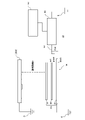
図1は、測定システム10における測定機器の接続図を模式的に示す。
図2は、測定システム10における各部の静電容量の関係を示す等価回路図を示す。
このような図1の測定システム10は、イオナイザ100が、除電によって除電対象物Wに引き起こす誘導電圧を測定できる。
<Measurement of Induced Voltage in Static Elimination Object>
FIG. 1 schematically shows a connection diagram of measuring devices in a measuring
FIG. 2 shows an equivalent circuit diagram showing the relationship of the capacitance of each part in the
Such a
具体的な誘起電圧の測定手順(1)~(3)は以下の通りである。
(1)図1に示す測定システム10の準備
□150mmの金属板22、24、26のそれぞれを用いて、絶縁した状態で3段構造を形成して、容量分圧式帯電プレート20を準備した。
容量分圧式帯電プレート20のそれぞれの金属板22、24、26を、三重同軸ケーブル30(TEKTRONIX社製、237-ALG-2)を介して、エレクトロメータ40(KEITHLEY社製、6517A)に接続した。エレクトロメータ40のアナログOUT端末を、ケーブルを介して、モニタ50(TEKTRONIX社製、オシロスコープ TDS503B)に接続した。
高圧電源Eを有する除電装置の一つとして、イオナイザ100を使用した。このイオナイザ100を、容量分圧式帯電プレート20の最上部の金属板22に対して、測定距離Dだけ離れた上部に配置した。
図1中、Gは接地を表す。図1の測定システム10の等価回路図を示す図2中の容量は、容量計を用いて測定した。
Specific procedures (1) to (3) for measuring the induced voltage are as follows.
(1) Preparation of
Each
An
In FIG. 1, G represents ground. The capacitance in FIG. 2 showing an equivalent circuit diagram of the
(2)容量分圧式帯電プレート20におけるVout、分圧比(C2/C1)の算出
図3は、誘導電圧の測定方法を説明するための図である。
電圧源E、上記(1)と同じ容量分圧式帯電プレート20、エレクトロメータ40を電気的に接続して、図3に示す測定システム12を準備した。図3中、Gは接地を表す。
測定システム12中、E0(V)に校正された直流の電圧源Eを金属板22に接続させ、金属板24をエレクトロメータ40に接続させた。
ここで、金属板22、24間の静電容量をC1とし、金属板24、26間の静電容量をC2とし、エレクトロメータ40で測定される出力電圧をVoutとした。
測定システム12中の接続回路は、式1:Vout=[C1/(C1+C2)]×E0を満たす。
式1から分圧比Pを表す式2:C2/C1=(E/Vout)-1が算出できる。
図3の測定システム12を用いて、Voutを測定し、得られたVoutの測定値から分圧比Pを求めた。
なお、電圧源Eから見た合成容量Ci(C1×C2/(C1+C2))が20pF±2pFの範囲ないとなり、C1が20.4pF、C2が460pFであった。容量は、容量計を用いて測定した。
(2) Calculation of V out and Voltage Division Ratio (C2/C1) in Capacitive Voltage Division
A measuring
In
Here, the capacitance between the
The connection circuitry in
Equation 2 representing the voltage division ratio P: C2/C1=(E/V out )−1 can be calculated from Equation 1.
Using the
The combined capacitance Ci (C1×C2/(C1+C2)) viewed from the voltage source E was within the range of 20 pF±2 pF, with C1 being 20.4 pF and C2 being 460 pF. Capacity was measured using a capacity meter.
(3)静電電圧の算出
図3中の電圧源Eを、所定のイオナイザ100に置き換えることによって、図1中の最上部の金属板22に静電誘導された誘導電圧Veiについては、図1中で測定されたVoutに、上記(2)で求められた分圧比Pを積算することによって求められる。すなわち、誘導電圧Veiは、式3:Vei=分圧比P×Voutに基づいて求められる。
以下、実験例1~4に示すイオナイザ、環境条件を採用して、図1中のVoutを測定し、そのVoutを使用して、式3に基づいて、誘導電圧Veiを算出した。
(3) Calculation of Electrostatic Voltage By replacing the voltage source E in FIG. 1 by adding the partial pressure ratio P obtained in (2) above to V out measured in 1. That is, the induced voltage V ei is obtained based on Equation 3: V ei =voltage division ratio P×V out .
The ionizers and environmental conditions shown in Experimental Examples 1 to 4 were employed to measure V out in FIG.
<比較例>
(実験例1)
温度:24℃、湿度:38%RH、測定距離D:100mm、エア圧力:無風の条件下で、上記(1)~(3)の手順に従って、図1の測定システム10中におけるVoutを測定し、最上部の金属板22に静電誘導された誘導電圧Veiを求めた。
図1の測定システム12中に使用したイオナイザ100の構造の概要を図4に示す。
図4は、使用したイオナイザ100の構造を模式的に示す断面図である。
実験例1で使用したイオナイザ(ACコロナ放電方式)は、ABS樹脂製の筐体110に収容された高圧電源120(交流型高圧電源、出力電圧:10kV0-p)と、10個の電極130(タングス製放電針、電極長さ:600mm、電極間のピッチ:250mm、)と、を有する。図5は、図4のα領域の拡大図を示す。図5に示す通り、ABS樹脂製のノズル部150の筒内部に電極130が配置されていて、ノズル部150の先端には、カバー部としてABS樹脂製のガード部160(ノズルガード)が装着されている。
実験例1の誘導電圧Veiは294Vp-pであった。
なお、ABS樹脂製の筐体110、ノズル部150、及びガード部160における表面抵抗率は、1016Ω/□であった。
<Comparative example>
(Experimental example 1)
Temperature: 24° C., Humidity: 38% RH, Measurement distance D: 100 mm, Air pressure: No wind, according to the procedures (1) to (3) above, measure V out in the
A schematic diagram of the construction of the
FIG. 4 is a cross-sectional view schematically showing the structure of the
The ionizer (AC corona discharge type) used in Experimental Example 1 includes a high-voltage power supply 120 (AC high-voltage power supply, output voltage: 10 kV 0-p ) housed in an
The induced voltage V ei in Experimental Example 1 was 294 Vpp .
The surface resistivity of the
<実施例>
(実験例2)
図4中の筐体110の表面112及び、図5中のノズル部150の表面152の全面において、静電気拡散性塗料Aを、エアスプレーガンを用いて塗布し、その表面に乾燥後の厚みが10μmとなるように塗膜を形成し、60℃のオーブンで1時間乾燥させて、静電気拡散性層Aを形成したイオナイザを使用した以外は、実験例1と同様にして、誘導電圧Veiを求めた。
実験例1の誘導電圧Veiは162Vp-pであった。
<Example>
(Experimental example 2)
4 and the
The induced voltage V ei in Experimental Example 1 was 162 Vpp .
(実験例3)
図4中の筐体110の表面112及び、図5中のノズル部150の表面152の全面において、静電気拡散性塗料Aを、エアスプレーガンを用いて塗布し、その表面に乾燥後の厚みが10μmとなるように塗膜を形成し、60℃のオーブンで1時間乾燥させて、静電気拡散性層Aを形成した点、図5中のガード部160の表面162の全面において、静電気拡散性塗料Bを、エアスプレーガンを用いて塗布し、その表面に乾燥後の厚みが10μmとなるように塗膜を形成し、60℃のオーブンで2時間乾燥させて、静電気拡散性層Bを形成した点、筐体110上の静電気拡散性層A及びガード部160上の静電気拡散性層Bを配線で電気的に接続した上で接地させた点を有するイオナイザを使用した以外は、実験例1と同様にして、誘導電圧Veiを求めた。
実験例1の誘導電圧Veiは52Vp-pであった。
(Experimental example 3)
4 and the
The induced voltage V ei in Experimental Example 1 was 52 Vpp .
(実験例4)
測定距離Dを300mmとした以外は、実験例3と同様にして、誘導電圧Veiを求めた。
実験例1の誘導電圧Veiは22Vp-pであった。
(Experimental example 4)
The induced voltage V ei was determined in the same manner as in Experimental Example 3, except that the measurement distance D was 300 mm.
The induced voltage V ei in Experimental Example 1 was 22 Vpp .
実施例である実験例3のイオナイザ(除電装置)を使用することによって、比較例である実験例1と比べて、イオナイザの静電誘導により除電対象物に発生する誘導電圧を低減できる結果を示した。 It is shown that the use of the ionizer (static eliminator) of Experimental Example 3, which is an example, can reduce the induced voltage generated in the static elimination target due to the electrostatic induction of the ionizer compared to Experimental Example 1, which is a comparative example. rice field.
また、実験例2~4において、ガード部160の表面抵抗率を104Ω/□、105Ω/□、107Ω/□、108Ω/□、109Ω/□に変更した場合でも、実験例1と比べて、イオナイザの静電誘導により除電対象物に発生する誘導電圧を低減できることが分かった。
Also, in Experimental Examples 2 to 4, when the surface resistivity of the
また、実験例2~4で使用したバー型のイオナイザ100(電圧印可式除電装置)において、電極長さを350mm、1600mm、3100mm、電極をシリコン製の放電針、又は電源を直流に仕様を変更した場合でも、それぞれは、同様の条件に仕様変更した実験例1と比べて、イオナイザの静電誘導により除電対象物に発生する誘導電圧を低減できることが分かった。 In addition, in the bar type ionizer 100 (voltage application type static eliminator) used in Experimental Examples 2 to 4, the electrode length was changed to 350 mm, 1600 mm, and 3100 mm, the electrode was changed to a silicon discharge needle, or the power supply was changed to direct current. It was found that even in these cases, the induced voltage generated in the object to be neutralized due to the electrostatic induction of the ionizer can be reduced compared to Experimental Example 1 in which the specifications were changed to the same conditions.
また、内蔵した除電電極と除電電極の先端を覆うABS樹脂製のノズルとを備える、ボックス型イオナイザ、ガン式イオナイザ、ペン型イオナイザ、又はノズル型イオナイザにおいて、当該ノズルの表面に静電気拡散性層Bを形成したものと、形成しないものを準備した。これらの静電気拡散性層を有するイオナイザは、ノズルの表面に静電気拡散性層Bを形成しないものと比較して、イオナイザの静電誘導により除電対象物に発生する誘導電圧を低減できることが分かった。 In a box-type ionizer, a gun-type ionizer, a pen-type ionizer, or a nozzle-type ionizer having a built-in static elimination electrode and an ABS resin nozzle covering the tip of the static elimination electrode, the static electricity diffusion layer B is provided on the surface of the nozzle. We prepared one that formed and one that did not. It was found that the ionizers having these static electricity dissipating layers can reduce the induced voltage generated in the object to be neutralized due to the electrostatic induction of the ionizers, compared to the ionizers not having the static electricity dissipating layer B formed on the surface of the nozzle.
内蔵した除電電極と除電電極の前方に設けられたABS樹脂製の正面ルーパーと後方に設けられたファンとを備える送風型イオナイザにおいて、当該正面ルーパーの表面に静電気拡散性層Bを形成したものと、形成しないものを準備した。静電気拡散性層を有する送風型イオナイザは、正面ルーパーの表面に静電気拡散性層Bを形成しないものと比較して、イオナイザの静電誘導により除電対象物に発生する誘導電圧を低減できることが分かった。 A blower type ionizer comprising a built-in neutralizing electrode, a front looper made of ABS resin provided in front of the neutralizing electrode, and a fan provided behind, in which a static electricity diffusion layer B is formed on the surface of the front looper. , prepared one that does not form. It was found that the blower ionizer having the static electricity dissipating layer can reduce the induced voltage generated in the object to be neutralized due to the static induction of the ionizer compared to the one without the static electricity dissipating layer B formed on the surface of the front looper. .
実施例のイオナイザ等の除電装置は、除電対象物の製造工程や組立工程中、その近傍に存在する除電対象物である電子部品・電子機器等において、除電時に発生する誘電帯電現象を緩和させることが可能である。 A static eliminator such as an ionizer according to the embodiments can alleviate the dielectric charging phenomenon that occurs during static elimination in electronic components, electronic equipment, etc., which are objects to be statically eliminated, which exist in the vicinity of the object to be statically eliminated during the manufacturing process or assembly process of the object to be statically eliminated. is possible.
10 測定システム
12 測定システム
20 容量分圧式帯電プレート
22、24、26 金属板
30 三重同軸ケーブル
40 エレクトロメータ
50 モニタ
100 イオナイザ(除電装置)
110 筐体
112 表面
120 高圧電源
130 電極
132 先端
134 開口
140 イオン
150 ノズル部
152 表面
160 ガード部
162 表面
170 配線部
180 静電気拡散性層
190 穴部
200 イオナイザ
210 筐体
220 高圧電源
230 電極
260 ノズル部材
270 配線部
300 イオナイザ
310 筐体
312 グリップ部
320 高圧電源
330 電極
360 ノズル部
370 配線部
400 イオナイザ
410 筐体
412 スイッチ部
420 高圧電源
430 電極
460 ノズル部
470 配線部
500 イオナイザ
510 筐体
512 チューブ部
520 高圧電源
530 電極
560 ノズル部
570 配線部
600 イオナイザ
610 筐体
620 高圧電源
630 電極
632 支持部
660 ルーパー部
670 配線部
680 ファン部
E 電圧源
W 除電対象物
10
110
Claims (16)
電気部品と、
前記電気部品に高圧電源の電力を送電する配線部と、
前記電気部品及び前記配線部を収容する筐体と、を備え、
前記電気部品の少なくとも一部を覆うカバー部を備え、前記カバー部の表面抵抗率が104Ω/□以上1011Ω/□以下となる構成、及び、前記筐体の表面抵抗率が104Ω/□以上1011Ω/□以下となる構成の少なくとも一方の構成を有しており、
前記筐体および前記カバー部の少なくとも一方が、
絶縁性、又は導電性の層と、
前記層の表面の少なくとも一部に形成された、表面抵抗率が10 4 Ω/□以上10 11 Ω/□以下の静電気拡散性層と、を有する、電子装置。 An electronic device used in the vicinity of an object to be statically removed,
electrical components;
a wiring unit for transmitting power from a high-voltage power supply to the electrical component;
A housing that accommodates the electrical component and the wiring unit,
A cover portion covering at least a portion of the electric component is provided, and the cover portion has a surface resistivity of 10 4 Ω/□ or more and 10 11 Ω/□ or less, and the housing has a surface resistivity of 10 4 . having at least one configuration of Ω/□ or more and 10 11 Ω/□ or less,
At least one of the housing and the cover is
an insulating or conductive layer;
and a static electricity dissipative layer having a surface resistivity of 10 4 Ω/□ or more and 10 11 Ω/□ or less formed on at least part of the surface of the layer.
電気部品と、 electrical components;
前記電気部品に高圧電源の電力を送電する配線部と、 a wiring unit for transmitting power from a high-voltage power supply to the electrical component;
前記電気部品及び前記配線部を収容する筐体と、を備え、 A housing that accommodates the electrical component and the wiring unit,
前記電気部品の少なくとも一部を覆うカバー部を備え、前記カバー部の表面抵抗率が10 A cover portion covering at least a portion of the electrical component is provided, and the surface resistivity of the cover portion is 10. 44 Ω/□以上10Ω/□ or more 10 1111 Ω/□以下となる構成、及び、前記筐体の表面抵抗率が10Ω/□ or less, and the surface resistivity of the housing is 10 44 Ω/□以上10Ω/□ or more 10 1111 Ω/□以下となる構成の少なくとも一方の構成を有しており、It has at least one configuration of Ω/□ or less,
前記筐体の表面抵抗率をAとし、前記カバー部の表面抵抗率をBとしたとき、 When the surface resistivity of the housing is A and the surface resistivity of the cover is B,
AおよびBが、10 A and B are 10 33 /10/10 1212 ≦A/B<1を満たす、電子装置。An electronic device satisfying ≦A/B<1.
前記筐体および前記カバー部の少なくとも一方が、
絶縁性、又は導電性の層と、
前記層の表面の少なくとも一部に形成された、表面抵抗率が104Ω/□以上1011Ω/□以下の静電気拡散性層と、を有する、電子装置。 The electronic device according to claim 2 ,
At least one of the housing and the cover is
an insulating or conductive layer;
and a static electricity dissipative layer having a surface resistivity of 10 4 Ω/□ or more and 10 11 Ω/□ or less formed on at least part of the surface of the layer.
前記静電気拡散性層が、静電気拡散性塗料からなる膜で構成される、電子装置。 The electronic device according to claim 1 or 3 ,
The electronic device, wherein the static electricity dissipative layer is composed of a film made of static electricity dissipative paint.
前記静電気拡散性塗料が、導電性成分とバインダー成分とを含む、電子装置。 The electronic device according to claim 4 ,
An electronic device, wherein the static electricity dissipative paint contains a conductive component and a binder component.
前記高圧電源が、交流発生回路を備える、電子装置。 The electronic device according to any one of claims 1 to 5 ,
An electronic device, wherein the high voltage power supply comprises an alternating current generation circuit.
前記カバー部の表面抵抗率が104Ω/□以上109Ω/□以下となる構成を有する、電子装置。 The electronic device according to any one of claims 1 to 6 ,
The electronic device, wherein the surface resistivity of the cover portion is 10 4 Ω/□ or more and 10 9 Ω/□ or less.
前記電気部品が、コロナ放電を発生させる電極、又はグロー放電を発生させる電極を含む、電子装置。 The electronic device according to any one of claims 1 to 7,
An electronic device, wherein the electrical component comprises an electrode for generating a corona discharge or an electrode for generating a glow discharge.
前記カバー部が、前記電極の周囲を覆うカバー構造、及び/又は前記電極の先端の前方を覆うカバー構造を有しており、前記カバー構造における表面抵抗率が104Ω/□以上1011Ω/□以下である、電子装置。 The electronic device according to claim 8,
The cover part has a cover structure that covers the periphery of the electrode and/or a cover structure that covers the front of the tip of the electrode, and the cover structure has a surface resistivity of 10 4 Ω/□ or more and 10 11 Ω. An electronic device that is less than or equal to /□.
第一の前記電極と、第二の前記電極と、第一の前記電極を覆う第一の前記カバー部と、第二の前記電極を覆う第二の前記カバー部と、を少なくとも備えており、
第一の前記カバー部と第二の前記カバー部とが電気的に接続するように構成される、電子装置。 The electronic device according to claim 9,
At least the first electrode, the second electrode, the first cover portion covering the first electrode, and the second cover portion covering the second electrode,
An electronic device, wherein the first cover part and the second cover part are configured to be electrically connected.
前記筐体に設けられており、前記電極の周囲を覆うように構成される、筒状のノズル部と、
前記筒状のノズル部に着脱自在に装着されており、前記電極の少なくとも先端を覆うように構成されるガード部と、を備えており、
前記カバー部が、前記筒状のノズル部と前記ガード部とで構成される、電子装置。 The electronic device according to any one of claims 8 to 10,
a cylindrical nozzle portion provided in the housing and configured to cover the periphery of the electrode;
a guard section detachably attached to the cylindrical nozzle section and configured to cover at least the tip of the electrode;
The electronic device, wherein the cover portion is composed of the cylindrical nozzle portion and the guard portion.
前記筐体と前記カバー部とが電気的に接続するように構成される、電子装置。 12. The electronic device of claim 11, comprising:
An electronic device, wherein the housing and the cover are configured to be electrically connected.
前記筐体がアースされた状態である、電子装置。 The electronic device according to any one of claims 1 to 12,
An electronic device, wherein the housing is grounded.
前記除電対象物が電子部品・電子機器であり、前記除電対象物の製造・組立工程における現場で用いられる、電子装置。 The electronic device according to any one of claims 1 to 13,
An electronic device, wherein the object to be statically eliminated is an electronic component or an electronic device, and is used on-site in a manufacturing/assembling process of the object to be statically eliminated.
前記筐体および前記カバー部の少なくとも一方において、絶縁性、又は導電性の層の表面に、表面抵抗率が10 4 Ω/□以上10 11 Ω/□以下の静電気拡散性塗料からなる膜を形成する膜形成工程と、
表面抵抗率が104Ω/□以上1011Ω/□以下であり、前記電気部品の少なくとも一部を覆うカバー部、及び表面抵抗率が104Ω/□以上1011Ω/□以下である前記筐体の少なくとも一方を用いて、電子装置の構成部品を組み立てることにより前記電子装置を得る、組立工程と、を含む、
電子装置の製造方法。 A method for manufacturing an electronic device used near an object to be neutralized, comprising an electric component, a wiring section for transmitting power of a high-voltage power supply to the electric component, and a housing for housing the electric component and the wiring section. and
In at least one of the housing and the cover, a film made of static dissipative paint having a surface resistivity of 10 4 Ω/□ or more and 10 11 Ω/□ or less is formed on the surface of the insulating or conductive layer. a film forming step for
The surface resistivity is 10 4 Ω/□ or more and 10 11 Ω/□ or less, and the surface resistivity of the cover portion that covers at least part of the electrical component is 10 4 Ω/□ or more and 10 11 Ω/□ or less. an assembling step of obtaining the electronic device by assembling components of the electronic device using at least one of the housings;
A method of manufacturing an electronic device.
表面抵抗率が10 surface resistivity is 10 44 Ω/□以上10Ω/□ or more 10 1111 Ω/□以下であり、前記電気部品の少なくとも一部を覆うカバー部、及び表面抵抗率が10Ω/□ or less, a cover portion that covers at least a portion of the electrical component, and a surface resistivity of 10 44 Ω/□以上10Ω/□ or more 10 1111 Ω/□以下である前記筐体の少なくとも一方を用いて、前記筐体の表面抵抗率をAとし、前記カバー部の表面抵抗率をBとしたとき、AおよびBが、10When at least one of the housings having Ω/□ or less is used and the surface resistivity of the housing is A and the surface resistivity of the cover portion is B, A and B are 10. 33 /10/10 1212 ≦A/B<1を満たすように、電子装置の構成部品を組み立てることにより前記電子装置を得る、組立工程を含む、An assembling step of obtaining the electronic device by assembling components of the electronic device so as to satisfy ≦A/B<1;
電子装置の製造方法。A method of manufacturing an electronic device.
Priority Applications (7)
| Application Number | Priority Date | Filing Date | Title |
|---|---|---|---|
| JP2020104857A JP7202575B2 (en) | 2020-06-17 | 2020-06-17 | ELECTRONIC DEVICE AND METHOD FOR MANUFACTURING ELECTRONIC DEVICE |
| KR1020227045191A KR20230024912A (en) | 2020-06-17 | 2021-06-16 | Electronic Devices and Methods of Manufacturing Electronic Devices |
| US18/010,629 US12309907B2 (en) | 2020-06-17 | 2021-06-16 | Electronic device and manufacturing method of electronic device |
| PCT/JP2021/022887 WO2021256513A1 (en) | 2020-06-17 | 2021-06-16 | Electronic device and method for manufacturing electronic device |
| CN202180042879.4A CN115836590B (en) | 2020-06-17 | 2021-06-16 | Electronic devices and methods of manufacturing electronic devices |
| TW110122098A TWI901702B (en) | 2020-06-17 | 2021-06-17 | Electronic devices and manufacturing methods for electronic devices |
| JP2022200933A JP7595326B2 (en) | 2020-06-17 | 2022-12-16 | Static electricity removal device |
Applications Claiming Priority (1)
| Application Number | Priority Date | Filing Date | Title |
|---|---|---|---|
| JP2020104857A JP7202575B2 (en) | 2020-06-17 | 2020-06-17 | ELECTRONIC DEVICE AND METHOD FOR MANUFACTURING ELECTRONIC DEVICE |
Related Child Applications (1)
| Application Number | Title | Priority Date | Filing Date |
|---|---|---|---|
| JP2022200933A Division JP7595326B2 (en) | 2020-06-17 | 2022-12-16 | Static electricity removal device |
Publications (2)
| Publication Number | Publication Date |
|---|---|
| JP2021197318A JP2021197318A (en) | 2021-12-27 |
| JP7202575B2 true JP7202575B2 (en) | 2023-01-12 |
Family
ID=79195922
Family Applications (2)
| Application Number | Title | Priority Date | Filing Date |
|---|---|---|---|
| JP2020104857A Active JP7202575B2 (en) | 2020-06-17 | 2020-06-17 | ELECTRONIC DEVICE AND METHOD FOR MANUFACTURING ELECTRONIC DEVICE |
| JP2022200933A Active JP7595326B2 (en) | 2020-06-17 | 2022-12-16 | Static electricity removal device |
Family Applications After (1)
| Application Number | Title | Priority Date | Filing Date |
|---|---|---|---|
| JP2022200933A Active JP7595326B2 (en) | 2020-06-17 | 2022-12-16 | Static electricity removal device |
Country Status (6)
| Country | Link |
|---|---|
| US (1) | US12309907B2 (en) |
| JP (2) | JP7202575B2 (en) |
| KR (1) | KR20230024912A (en) |
| CN (1) | CN115836590B (en) |
| TW (1) | TWI901702B (en) |
| WO (1) | WO2021256513A1 (en) |
Cited By (1)
| Publication number | Priority date | Publication date | Assignee | Title |
|---|---|---|---|---|
| JP7595326B2 (en) | 2020-06-17 | 2024-12-06 | 株式会社松本技研 | Static electricity removal device |
Families Citing this family (2)
| Publication number | Priority date | Publication date | Assignee | Title |
|---|---|---|---|---|
| US20250183627A1 (en) * | 2023-12-04 | 2025-06-05 | Hamilton Sundstrand Corporation | Ion emitter system |
| JP2025129837A (en) | 2024-02-26 | 2025-09-05 | 三星電子株式会社 | Charging device and electrostatic precipitator |
Citations (5)
| Publication number | Priority date | Publication date | Assignee | Title |
|---|---|---|---|---|
| JP2001203094A (en) | 2000-01-17 | 2001-07-27 | Sharp Corp | Ionizer |
| JP2005142131A (en) | 2003-11-10 | 2005-06-02 | Fuji Photo Film Co Ltd | Static eliminator |
| JP2007234437A (en) | 2006-03-02 | 2007-09-13 | Trinc:Kk | Plasma discharge type static eliminator |
| JP2013054983A (en) | 2011-09-06 | 2013-03-21 | Panasonic Corp | Discharge electrode, active species generating unit using the same, and active species generating device |
| JP2019075349A (en) | 2017-10-19 | 2019-05-16 | Smc株式会社 | Ionizer |
Family Cites Families (30)
| Publication number | Priority date | Publication date | Assignee | Title |
|---|---|---|---|---|
| DE2064545C3 (en) * | 1970-12-30 | 1980-06-19 | Hoechst Ag, 6000 Frankfurt | Device for electrostatically charging or discharging surfaces of a material |
| JPH05226092A (en) * | 1992-02-07 | 1993-09-03 | Matsushita Electric Ind Co Ltd | Electrostatic diffusion resin complex |
| EP0502483A3 (en) | 1991-03-05 | 1993-01-20 | Matsushita Electric Industrial Co., Ltd. | Static dissipative resin composition |
| JPH04306674A (en) * | 1991-04-03 | 1992-10-29 | Konica Corp | Static eliminator device |
| JP3080116B2 (en) | 1992-08-25 | 2000-08-21 | 高砂熱学工業株式会社 | Device for neutralizing charged articles |
| JPH06231897A (en) * | 1993-02-05 | 1994-08-19 | Seiko Epson Corp | Static electricity erasing method and device therefor |
| JPH10144450A (en) * | 1996-11-12 | 1998-05-29 | Kazuo Okano | Electric discharge electrode for ion producing device |
| JP2002025791A (en) * | 2000-07-12 | 2002-01-25 | Hugle Electronics Inc | Ac power source type ionizer |
| JP2002289394A (en) | 2001-03-27 | 2002-10-04 | Toray Ind Inc | Insulating sheet static elimination method and apparatus |
| KR101111468B1 (en) | 2003-06-05 | 2012-02-21 | 시시도 세이덴기 가부시키가이샤 | Ion generator |
| JP2005222868A (en) | 2004-02-06 | 2005-08-18 | Taiheiyo Cement Corp | Ion generating device |
| JP2005243558A (en) | 2004-02-27 | 2005-09-08 | Pentel Corp | Static eliminator |
| US20080273282A1 (en) | 2006-03-02 | 2008-11-06 | Makoto Takayanagi | Dbd plasma discharged static eliminator |
| JP4904451B2 (en) * | 2007-03-27 | 2012-03-28 | セイコーインスツル株式会社 | Antistatic materials, portable electronic devices and electronic watches |
| JP5178114B2 (en) * | 2007-09-28 | 2013-04-10 | ヒューグルエレクトロニクス株式会社 | Electrode unit and ionizer |
| JP2009099472A (en) * | 2007-10-18 | 2009-05-07 | Shishido Seidenki Kk | Blast type ion generating device |
| JP2011065747A (en) * | 2008-01-15 | 2011-03-31 | Tokai Industry Corp | Static eliminator |
| US9380689B2 (en) * | 2008-06-18 | 2016-06-28 | Illinois Tool Works Inc. | Silicon based charge neutralization systems |
| JP2011238553A (en) | 2010-05-13 | 2011-11-24 | Oriental Motor Co Ltd | Static eliminator using fan motor |
| JP5661542B2 (en) * | 2011-04-08 | 2015-01-28 | 株式会社キーエンス | Static eliminator |
| JP2012221901A (en) | 2011-04-14 | 2012-11-12 | Keyence Corp | Static eliminator and discharge needle unit |
| JP2014010946A (en) | 2012-06-28 | 2014-01-20 | Sharp Corp | Static eliminator |
| CN202704681U (en) * | 2012-08-27 | 2013-01-30 | 上海美声服饰辅料有限公司 | Destaticization mechanism applied to manufacturing process of RFID (Radio Frequency Identification Device) label |
| JP6469988B2 (en) * | 2014-07-30 | 2019-02-13 | 三菱航空機株式会社 | Aircraft antenna cover and aircraft |
| JP2016072051A (en) | 2014-09-30 | 2016-05-09 | 春日電機株式会社 | Gun-type static eliminator |
| KR20180047162A (en) | 2016-10-31 | 2018-05-10 | 주식회사 대창 | Air cleaning apparatus for overhead type consol of car |
| JP2018088189A (en) * | 2016-11-29 | 2018-06-07 | パナソニックIpマネジメント株式会社 | Static eliminator, authentication system, ic card, and card reader |
| JP6725938B2 (en) | 2017-04-28 | 2020-07-22 | シシド静電気株式会社 | Ion generator |
| GB2585921A (en) * | 2019-07-24 | 2021-01-27 | Linx Printing Tech | Continuous Ink Jet printer and print head assembly therefor |
| JP7202575B2 (en) | 2020-06-17 | 2023-01-12 | 株式会社松本技研 | ELECTRONIC DEVICE AND METHOD FOR MANUFACTURING ELECTRONIC DEVICE |
-
2020
- 2020-06-17 JP JP2020104857A patent/JP7202575B2/en active Active
-
2021
- 2021-06-16 KR KR1020227045191A patent/KR20230024912A/en active Pending
- 2021-06-16 WO PCT/JP2021/022887 patent/WO2021256513A1/en not_active Ceased
- 2021-06-16 US US18/010,629 patent/US12309907B2/en active Active
- 2021-06-16 CN CN202180042879.4A patent/CN115836590B/en active Active
- 2021-06-17 TW TW110122098A patent/TWI901702B/en active
-
2022
- 2022-12-16 JP JP2022200933A patent/JP7595326B2/en active Active
Patent Citations (5)
| Publication number | Priority date | Publication date | Assignee | Title |
|---|---|---|---|---|
| JP2001203094A (en) | 2000-01-17 | 2001-07-27 | Sharp Corp | Ionizer |
| JP2005142131A (en) | 2003-11-10 | 2005-06-02 | Fuji Photo Film Co Ltd | Static eliminator |
| JP2007234437A (en) | 2006-03-02 | 2007-09-13 | Trinc:Kk | Plasma discharge type static eliminator |
| JP2013054983A (en) | 2011-09-06 | 2013-03-21 | Panasonic Corp | Discharge electrode, active species generating unit using the same, and active species generating device |
| JP2019075349A (en) | 2017-10-19 | 2019-05-16 | Smc株式会社 | Ionizer |
Cited By (1)
| Publication number | Priority date | Publication date | Assignee | Title |
|---|---|---|---|---|
| JP7595326B2 (en) | 2020-06-17 | 2024-12-06 | 株式会社松本技研 | Static electricity removal device |
Also Published As
| Publication number | Publication date |
|---|---|
| TW202220319A (en) | 2022-05-16 |
| JP7595326B2 (en) | 2024-12-06 |
| US12309907B2 (en) | 2025-05-20 |
| TWI901702B (en) | 2025-10-21 |
| JP2021197318A (en) | 2021-12-27 |
| WO2021256513A1 (en) | 2021-12-23 |
| US20230345608A1 (en) | 2023-10-26 |
| CN115836590B (en) | 2026-03-31 |
| JP2023030053A (en) | 2023-03-07 |
| CN115836590A (en) | 2023-03-21 |
| KR20230024912A (en) | 2023-02-21 |
Similar Documents
| Publication | Publication Date | Title |
|---|---|---|
| JP7595326B2 (en) | Static electricity removal device | |
| CA1303345C (en) | Apparatus for coating workpieces electrostatically | |
| CN101842167B (en) | Electrostatic coating apparatus | |
| JP2011060537A (en) | Static eliminator | |
| JP2012520753A5 (en) | ||
| JP2012520753A (en) | Electrode assembly for electrostatic sprayer | |
| JP5535007B2 (en) | Ionizer module | |
| CN104349843A (en) | Electrostatic painting apparatus | |
| JP2015028938A (en) | Electrostatic charge dissipation system | |
| JP2023030053A5 (en) | static eliminator | |
| TW200413101A (en) | Spray gun for electrostatic painting | |
| JP6071506B2 (en) | Thin film forming equipment | |
| JPH08506535A (en) | Improved printhead for inkjet printers | |
| JP4645375B2 (en) | Electrostatic coating equipment | |
| US9001487B2 (en) | Ionizer | |
| JPWO2017141474A1 (en) | Gas insulated electrical equipment | |
| JPH06124792A (en) | Antistatic electrode | |
| JP4002948B2 (en) | Ion generator | |
| CN104429167A (en) | Eliminator | |
| RU2664224C1 (en) | Covered ironing plate and method for manufacturing covered ironing plate | |
| WO2022247489A1 (en) | Radiation processing method for electrostatic discharge simulator, and electrostatic discharge simulator | |
| US20160196949A1 (en) | Atmospheric ionizer including a source that supplies electrical energy to an ion-generating structure without wires | |
| US20140306035A1 (en) | Electrode assembly and electrostatic atomizer having such an electrode assembly | |
| Klouda | Practical Electromagnetic Shielding of Plastic Cases | |
| JPH05210283A (en) | Contact electrification method and contact electrification device |
Legal Events
| Date | Code | Title | Description |
|---|---|---|---|
| A621 | Written request for application examination |
Free format text: JAPANESE INTERMEDIATE CODE: A621 Effective date: 20220721 |
|
| A871 | Explanation of circumstances concerning accelerated examination |
Free format text: JAPANESE INTERMEDIATE CODE: A871 Effective date: 20220721 |
|
| A131 | Notification of reasons for refusal |
Free format text: JAPANESE INTERMEDIATE CODE: A131 Effective date: 20220906 |
|
| A521 | Request for written amendment filed |
Free format text: JAPANESE INTERMEDIATE CODE: A523 Effective date: 20221104 |
|
| TRDD | Decision of grant or rejection written | ||
| A01 | Written decision to grant a patent or to grant a registration (utility model) |
Free format text: JAPANESE INTERMEDIATE CODE: A01 Effective date: 20221122 |
|
| A61 | First payment of annual fees (during grant procedure) |
Free format text: JAPANESE INTERMEDIATE CODE: A61 Effective date: 20221216 |
|
| R150 | Certificate of patent or registration of utility model |
Ref document number: 7202575 Country of ref document: JP Free format text: JAPANESE INTERMEDIATE CODE: R150 |
|
| S531 | Written request for registration of change of domicile |
Free format text: JAPANESE INTERMEDIATE CODE: R313531 |
|
| R350 | Written notification of registration of transfer |
Free format text: JAPANESE INTERMEDIATE CODE: R350 |
|
| R250 | Receipt of annual fees |
Free format text: JAPANESE INTERMEDIATE CODE: R250 |