JP2018514787A - Voltage sensor - Google Patents
Voltage sensor Download PDFInfo
- Publication number
- JP2018514787A JP2018514787A JP2017559801A JP2017559801A JP2018514787A JP 2018514787 A JP2018514787 A JP 2018514787A JP 2017559801 A JP2017559801 A JP 2017559801A JP 2017559801 A JP2017559801 A JP 2017559801A JP 2018514787 A JP2018514787 A JP 2018514787A
- Authority
- JP
- Japan
- Prior art keywords
- voltage sensor
- voltage
- conductor
- sensor
- section
- Prior art date
- Legal status (The legal status is an assumption and is not a legal conclusion. Google has not performed a legal analysis and makes no representation as to the accuracy of the status listed.)
- Pending
Links
Images

Classifications
-
- G—PHYSICS
- G01—MEASURING; TESTING
- G01R—MEASURING ELECTRIC VARIABLES; MEASURING MAGNETIC VARIABLES
- G01R19/00—Arrangements for measuring currents or voltages or for indicating presence or sign thereof
- G01R19/0084—Arrangements for measuring currents or voltages or for indicating presence or sign thereof measuring voltage only
-
- G—PHYSICS
- G01—MEASURING; TESTING
- G01R—MEASURING ELECTRIC VARIABLES; MEASURING MAGNETIC VARIABLES
- G01R15/00—Details of measuring arrangements of the types provided for in groups G01R17/00 - G01R29/00, G01R33/00 - G01R33/26 or G01R35/00
- G01R15/14—Adaptations providing voltage or current isolation, e.g. for high-voltage or high-current networks
- G01R15/16—Adaptations providing voltage or current isolation, e.g. for high-voltage or high-current networks using capacitive devices
Landscapes
- Physics & Mathematics (AREA)
- General Physics & Mathematics (AREA)
- Measuring Instrument Details And Bridges, And Automatic Balancing Devices (AREA)
Abstract
電圧センサは、第1端部(101)及び第2端部(103)を有する導体(102)を備え、第1端部は第1接続インターフェース(150)を含み、第2端部は接続を有さず、センサ区分(125)は、導体上に配置された少なくとも1つのセンサを含み、センサは少なくとも、導体の電圧、又は電圧のサンプルを感知する。電圧センサは、電力線若しくはケーブル、例えば、高架電力線若しくはケーブル、又はケーブル付属品、に接続可能であり、地下用途にも使用することができる。The voltage sensor includes a conductor (102) having a first end (101) and a second end (103), the first end includes a first connection interface (150), and the second end connects. Without, the sensor section (125) includes at least one sensor disposed on the conductor, the sensor sensing at least the voltage of the conductor, or a sample of the voltage. The voltage sensor can be connected to a power line or cable, such as an overhead power line or cable, or cable accessory, and can also be used for underground applications.
Description
本発明は、電力線及び/又はケーブル付属品の用途のための、電圧センサに関する。 The present invention relates to voltage sensors for power line and / or cable accessory applications.
電力の分配は、再生可能エネルギーや分散型発電の出現、及び電気自動車の採択によってより複雑化し、インテリジェントな配電及びそれに関連する電気的検知はより有用になり、必須にさえなってきている。有用な検知としては、例えば、配電網内の様々な位置での、電圧、電流、及び電圧と電流との間の時間関係が挙げられ得る。 Power distribution has become more complex with the advent of renewable energy and distributed generation, and the adoption of electric vehicles, and intelligent power distribution and associated electrical sensing has become more useful and even mandatory. Useful sensing can include, for example, voltage, current, and time relationship between voltage and current at various locations within the distribution network.
一般的に、本開示は、電力線、ケーブル、又はケーブル付属品に接続され得る、電圧センサを対象とする。特に、電圧センサは、第1端部及び第2端部を有する導体を備え、第1端部は第1接続インターフェースを含み、第2端部は接続を有さず、センサ区分は、導体上で第1端部と第2端部との間に配置された少なくとも1つのセンサを含み、センサは少なくとも、導体の電圧、又は電圧のサンプルを感知する。 In general, the present disclosure is directed to voltage sensors that can be connected to power lines, cables, or cable accessories. In particular, the voltage sensor includes a conductor having a first end and a second end, the first end includes a first connection interface, the second end has no connection, and the sensor section is on the conductor. At least one sensor disposed between the first end and the second end, wherein the sensor senses at least a voltage of the conductor, or a sample of the voltage.
一態様において、第2端部は、より低い電界ストレス集中度を有する。更なる態様において、導体の第2端部は、丸い表面、例えば、完全に丸い(又は半球の)表面を有する。更なる態様において、第2端部は、球根状の丸い表面を含む。 In one aspect, the second end has a lower field stress concentration. In a further aspect, the second end of the conductor has a rounded surface, eg, a completely rounded (or hemispherical) surface. In a further aspect, the second end includes a bulbous round surface.
一態様において、センサ区分は、電圧センサを含む。電圧センサの第1電極は、導体を含み得る。あるいは、電圧センサの第1電極は、導体と接触した内側遮蔽層を備える。電圧センサは更に、絶縁された内側遮蔽層の上に配置された絶縁層と、絶縁層の上に配置された、電気的に絶縁された外側遮蔽層とを含む。 In one aspect, the sensor section includes a voltage sensor. The first electrode of the voltage sensor can include a conductor. Alternatively, the first electrode of the voltage sensor includes an inner shielding layer in contact with the conductor. The voltage sensor further includes an insulating layer disposed over the insulated inner shielding layer and an electrically isolated outer shielding layer disposed over the insulating layer.
本発明の上記の概要は、本発明の各例示される実施形態又は全ての実現形態を説明することを目的とするものではない。本開示の1つ以上の実施例の詳細を添付図面及び以下の説明に示す。本開示の技法の他の特徴、目的、及び利点は、発明を実施するための形態及び図面、並びに特許請求の範囲から明らかとなるであろう。 The above summary of the present invention is not intended to describe each illustrated embodiment or every implementation of the present invention. The details of one or more embodiments of the disclosure are set forth in the accompanying drawings and the description below. Other features, objects, and advantages of the techniques of this disclosure will be apparent from the detailed description and drawings, and from the claims.
以下の発明を実施するための形態では、本明細書の一部を構成する添付の図面を参照し、本発明を実施することができる特定の実施形態を例として示す。その際、「上」、「下」、「前」、「後」、「前縁」、「前方」、「後縁」などの方向に関する用語は、説明する図面の方向を基準として用いられている。本発明の各実施形態の構成要素は多数の様々な方向で位置決めされ得るため、方向に関する用語は、説明の目的で用いられており、限定するものではない。他の実施形態を利用することもでき、また、構造的又は論理的な変更が、本発明の範囲から逸脱することなくなされ得ることが理解される。したがって、以下の詳細な説明は、限定的な意味で解釈されるべきではなく、本発明の範囲は、添付の特許請求の範囲によって定義される。 In the following detailed description, reference is made to the accompanying drawings that form a part hereof, and in which is shown by way of illustration specific embodiments in which the invention may be practiced. At that time, terms related to directions such as “up”, “down”, “front”, “rear”, “front edge”, “front”, “rear edge” are used with reference to the direction of the drawing to be described. Yes. Because the components of each embodiment of the present invention can be positioned in a number of different directions, the terminology related to direction is used for purposes of explanation and is not limiting. It will be understood that other embodiments may be utilized and structural or logical changes may be made without departing from the scope of the present invention. The following detailed description is, therefore, not to be taken in a limiting sense, and the scope of the present invention is defined by the appended claims.
本開示は、コンデンサバンク、スイッチ、又は保護装置、例えば、高架スイッチ(手動、又はモータによって起動される、ソレノイドなど)、セクショナライザ若しくはリクローザ、又は電圧調節変換器など、特定の位置において、高架電力線などの電力線の電圧を測定するために使用することができる電圧センサについて記載している。電圧センサは、小型の設計を有することがあり、単純な方法で既存の電力線(導体又はケーブル)に接続することができる。本明細書において記載される電圧センサは、電力ケーブル又は電気グリッド中の位置の電圧の特性をリアルタイムで高精度に供給するためのコンパクトな機構を提供することができる。電圧センサの出力は、電力線の電圧と正比例する波形であり得る。実際の線電圧の、出力電圧に対する分圧比は、任意の所望の電圧に調節することができる。幾つかの実施形態では、分圧比は、1:1〜1,000,000:1であり得る。他の好ましい実施形態において、分圧比はおよそ10000:1であり得、例えば、およそ10000Vの実際の線間電圧は、およそ1Vの出力電圧を生じる。電圧センサは、いくつかの実施形態において、演算装置、マイクロコントローラ、通信装置などと相互作用するために、デジタル値に容易に変換することができる電圧レベルを供給する。電圧センサはしたがって、設備、太陽光発電所、風力発電所、船、工場、又は中若しくは高電圧設備を使用するいずれかの個人又は法人に、電気が流れている電力線のリアルタイムの電圧読み取りを得るための容易なアクセスをもたらし、多くの異なるグリッド位置においてスマートノードを形成する能力をもたらす。 The present disclosure relates to an elevated power line at a particular location, such as a capacitor bank, switch, or protection device, such as an elevated switch (such as a solenoid that is manually or activated by a motor), a sectionizer or recloser, or a voltage regulated transducer. A voltage sensor that can be used to measure the voltage of a power line is described. Voltage sensors may have a compact design and can be connected to existing power lines (conductors or cables) in a simple manner. The voltage sensors described herein can provide a compact mechanism for supplying voltage characteristics at a location in a power cable or electrical grid with high accuracy in real time. The output of the voltage sensor can be a waveform that is directly proportional to the voltage of the power line. The division ratio of the actual line voltage to the output voltage can be adjusted to any desired voltage. In some embodiments, the partial pressure ratio can be 1: 1 to 1,000,000: 1. In other preferred embodiments, the voltage division ratio may be approximately 10,000: 1, for example, an actual line voltage of approximately 10000V will result in an output voltage of approximately 1V. The voltage sensor, in some embodiments, provides a voltage level that can be easily converted to a digital value to interact with computing devices, microcontrollers, communication devices, and the like. The voltage sensor thus obtains a real-time voltage reading of the power line through which electricity is flowing to the facility, solar power plant, wind power plant, ship, factory, or any individual or corporation using medium or high voltage equipment Provides the ability to form smart nodes at many different grid locations.
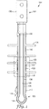
図1は、本発明の第1態様における、電圧センサ100を示している。
FIG. 1 shows a
電圧センサ100は、アルミニウム、又は銅合金導体などの、中実の、又は撚り合わせた金属軸方向導体であり得る、導体(内部導体とも称される)102を含む。内側導体102は、第1接続インターフェース150を含む第1端部101、及び第2端部103を含み得る。第2端部103は、接続部を有さない。一態様において、第2端部は、部分的な放電、又は電気的故障の可能性を実質的に低減するために、最小の空間で、容易に、最適なストレス制御を可能にするような形状である。一態様において、第2端部103は、丸い表面105、例えば、完全に丸い表面(すなわち、鋭い縁部を有さない、又は殆ど有さない)を含む。この丸い表面形状は、電界ストレスの集中を低減する。図1に示されるように、1つの代表的な構成において、丸い表面105は球根の形状を有する。あるいは、導体102の大きさによって、導体102が十分に大きな直径を有する場合、球根状の端部は不要と成り得る。代わりに、いくつかの実施形態において、全半径(半球)が、導体の端部103から形成されてもよい。この半球の形状は、電気ストレスの集中につながり得る、いずれかの鋭い縁部を排除する。更なる代替的な態様において、電圧センサ100の第2端部103は、成形された、半導電性ゴム又は半導電性プラスチック材料で被覆することができる。この代替的な態様において、半導電性成形を使用して、丸い表面又は鋭い表面を被覆することができる。
The
第1接続インターフェース150は、図1に示されるラグを含み得る。あるいは、接続インターフェースは、分離可能なコネクタ、スプライス、モジュラーコネクタ、又は他の接続インターフェースを備え得る。
The
接続インターフェースは、導体102の雄型端部と係合するように構成された円形断面を有し得る。別の態様において、導体102の第1端部は、雄型、又は複合タイプのコネクタとして形成され得る。
The connection interface may have a circular cross section configured to engage the male end of the
図1に示されるように、接続インターフェース150はラグを備える。図1の構造は、高架電力ケーブル、又は電力線との単純な機械的締結、及びここからの電気伝動(又は経路)を可能にする。例えば、電圧センサ100を、高架線に取り付ける1つの方法は、従来的な高架主要タップ(Hubbell Power Systems,USAから入手可能なBHF/AHF2穴ホットラインパッドコネクタなど)を使用し、このコネクタを接続インターフェース/ラグ150へとボルトで固定するものである。あるいは、従来的なステムコネクタを使用することができる。したがって、電圧センサ100は、電力ケーブル、電力線に沿ったいずれかの点、又はケーブル付属品内に設置することができる。
As shown in FIG. 1, the
更に、電圧センサ100は、例えば、高架電力線、又は高架電力ケーブル(電力線又は電力ケーブルは、1000ボルトを超える電圧で動作する)などの電力線又はケーブル内の中電圧又は高電圧によって生じた電界を制御するように構成される。図1に示されるように、電界を制御するために、高誘電率層132を利用することができる。あるいは、電圧センサ100は、幾何学的ストレス制御(図示されない)を含み得る。
Furthermore, the
任意により、いくつかの態様において、内側導体102は、導体遮蔽層104によって半径方向で包囲されてもよい。導体遮蔽層104は、特に、中又は高電圧線又はケーブルの電圧を感知する際に、高い電界ストレス集中を生じる可能性がある(これは、精度の低下、又は場合によりセンサの故障を生じ得る)、いずれかの導体表面の非平坦性を平滑にするように構成された、導電性、又は半導電性材料を備える。一態様において、導体遮蔽層104の外側表面は平滑である。以下で更に詳細に記載されるように、内側導体102、及び任意選択の内側遮蔽層104は、センサ区分のコンデンサの1つの電極をもたらす。コンデンサの他の電極は、絶縁遮蔽層108の絶縁区分110によって形成され、絶縁層106は、コンデンサの誘電体として機能する。
Optionally, in some aspects, the
電圧センサ100は、絶縁層106を更に含み、これは導体遮蔽層104を同心状に囲む。絶縁層106は、エラストマーシリコーン、エチレンプロピレンジエンモノマーゴム(EPDM)、混合物、又はこれらの組み合わせなど、従来的な誘電材料から形成され得る。あるいは、絶縁層106は、第1及び第2絶縁層(図示されない)など、2層以上の絶縁材料を備えてもよく、各層は、異なる又は同じ絶縁材料から形成される。任意の半導電性、又は導電性遮蔽層104は、導体102と、絶縁層106との間に空隙(これは、絶縁層106の劣化につながる漏れを生じ得る)が生じる可能性を排除、又は低減するように機能する。遮蔽層104はまた、例えば、キャストなどの製造プロセスによる、内側導体102の表面上のいずれかの粗さによって生じる、電気ストレスを軽減することができる。
The
別の態様において、導電性層102は、非常に平滑な外側表面を有し得る。したがって、接着剤又は他の結合材料は、導電性層102と、絶縁層106との間に介在し、遮蔽層104が排除されてもよい。接着剤又は他の結合材料が、導体102の外側表面に適用されてもよく、絶縁層106を導電性層102に結合してもよい。
In another aspect, the
加えて、絶縁遮蔽層108が設けられ、絶縁層106を同心状に囲む。絶縁遮蔽層108は、絶縁層106に隣接して、これを同心状に囲む層として形成された、導電性又は半導電性材料を備える。以下に記載されるように、感知区分125の目的のために、絶縁層106はまたコンデンサの絶縁層を形成し、これは、内側導体102、並びに/又は導体遮蔽層104、及び絶縁遮蔽層108の絶縁区分110を備える。絶縁遮蔽層110の絶縁された区分は、絶縁遮蔽層108の残部の地電位から絶縁されている。
In addition, an insulating
図1の実施形態では、電圧センサ100は、導体/内側遮蔽/絶縁体/遮蔽構造、及びセンサ区分125の少なくとも一部分にわたって延びる、管状スリーブ112を更に備える。一態様において、管状スリーブ112は、好適な常温収縮材料、例えば、EPDMなどの低い永久歪みを有する、非常に弾性的なゴム材料、エラストマーシリコーン、電気材料として使用可能な品位の樹脂、又はこれらの複合物など、を含む。絶縁層106、及び管状スリーブは、同じ又は異なる種類の材料で作製することができる。半導電性材及び絶縁材は、使用される材料の固有の特性に基づいて、又は材料に添加される添加剤に基づいて、異なる程度の導電性及び絶縁性を有し得る。管状スリーブ112はまた、好適な熱収縮材料から作製することもできる。代替的に、管状スリーブ112は、オーバーモールド層又はプッシュオン層であってもよい。接地基準ワイヤ115もまた、設けられてもよい。任意により、例示される実施形態において、管状スリーブ112は、漏洩電流を低減するように機能し、屋外用途に特に有用な、スカート135を含む。いくつかの実施形態において、管状スリーブ112はまた、丸い端部103を被覆することができる。
In the embodiment of FIG. 1,
加えて、封止化合物130は、環境封止を形成し、かつ絶縁層106と、接続インターフェース/ラグ150との間の領域内に水分が移動するのを防ぐために設けられることがある。
In addition, the sealing
図1に示され、図2により詳細に示されるように、電圧センサ100は、導体102の第1端部と第2端部との間に配置されたセンサ区分125を含む。一態様において、感知区分は、複素インピーダンスに基づく分圧を使用する、インピーダンス分圧器、又は電気的に絶縁された容量電圧センサを有する、容量電圧感知装置などの電圧センサを含む。より一般的に、感知区分がインピーダンス分圧器を含む、少なくとも一態様において、第1インピーダンス及び第2インピーダンスが、直列接続される。入力電圧が直列インピーダンスに適用され、出力電圧は、第2インピーダンスでの電圧である。第1インピーダンス及び第2インピーダンスは、レジスタ、インダクタ、及びコンデンサなどの、素子のいずれかの組み合わせで構成されてもよい。少なくとも一態様において、感知区分は多成分AC回路を含み、応答は複素数であり得、虚数成分を有することがある。別の態様において、センサ区分は、例えば、サーミスタなど、少なくとも1つの温度補償要素を含む。温度センサ(例えば、サーミスタ)は、感知区分125の内部(又は外部)に位置してもよい。1つの特定の実施形態が以下に記載されるが、国際公開第2015/179285号、及び同第2013/096354号に記載される電圧センサと同様の方法で構成されてもよく、それぞれ本明細書においてその全体が組み込まれる。更に、別の態様において、電圧センサ100は更に、1つ以上の追加のセンサを含んでもよい。
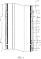
As shown in FIG. 1 and shown in more detail in FIG. 2,
図2に示されるように、感知区分125は、絶縁層106の外側表面と接触する、導電性又は半導電性材料(絶縁遮蔽)層108の電気的に絶縁された区分110を含む。導電性、又は半導電性材料(絶縁遮蔽)層108の電気的に絶縁された区分110は、容量性分圧器又はセンサの感知コンデンサの電極を形成している。電気的に絶縁された区分はしたがって、導電体102に容量結合され、地電位から電気的に絶縁され得る。加えて、絶縁層106は、容量性分圧器又はセンサの感知コンデンサの誘電体を形成するように動作可能である。
As shown in FIG. 2, the
いくつかの実施例において、電気的に絶縁された区分110は、環状リング構成であり、非導電性軸方向区分111a及び111bによって、導電性又は半導電性遮蔽層108から電気的に絶縁されていてもよい。これらの非導電性軸方向区分111a、111bは、非導電性材料又は間隙を含んでもよい。
In some embodiments, the electrically
このような実施例において、導電性又は半導電性遮蔽層108は、環状リング構成において、電気的に分離された区分110を形成するように、2つの長手方向位置において断絶していてもよい。このような実施例において、電気的に絶縁された区分110は、電気的に絶縁された区分110及び遮蔽層108が一般的な厚さを有するように、一般的な材料及び製造プロセスによって形成されてもよい。
In such an embodiment, the conductive or
他の実施例において、電気的に絶縁された区分110は、遮蔽層108とは異なる材料から形成されてもよく、及び/又は絶縁層106に固定された可撓性材料から形成された、矩形、又は丸い形状などの異なる構成を有してもよい。電気的に絶縁された区分110は例えば、導電性金属又は導電性ポリマーを含んでもよい。一実施例として、電気的に絶縁された区分110は、銅の層を含んでもよい。いくつかの実施例において、電圧センサ100は、電気的に絶縁された区分110を絶縁層106に固定する接着剤を含んでもよい。いくつかの実施例において、電気的に絶縁された区分110は更に、水分がセンサ区分125に移動するのを防ぐため、適合するゴム絶縁体、又は高誘電率のテープ、又は自己融着絶縁体、又は高誘電率材料127(例えば、ゴムマスチック材料)を含んでもよい。絶縁、又は高誘電率材料のストリップは、間隙111a、111bを被覆して、絶縁区分110を、PCB120以外の任意の他の導電性又は半導電性材料又は要素から分離し、間隙111a、111b内に空気が存在するのを防止するが、この空気は、電圧センサの部分的な放電及び故障の原因となり得る。絶縁材料、又は高誘電率材料は、空隙111a、111bをより容易にふさぐマスチック及びマスチック上に配置されたPVCテープの組み合わせなどの任意の好適な材料であってもよい。いくつかの実施例において、電気的に絶縁された区分110は、熱収縮又は常温収縮材料を含むことがある。
In other embodiments, the electrically
いくつかの態様において、電圧センサ100の、内側及び外側導電性、又は半導電性遮蔽層104、108、並びに絶縁層106は、収縮スリーブの用途に好適な任意の材料から作製されてもよい。最も好適なのは、エチレンプロピレンジエンモノマー(EPDM)、エラストマーシリコーン、又はこれらの混合物のような、低い永久歪を有する高弾性ゴムのような材料であり、これらは、必要に応じて層を適切に導電性、半導電性、又は絶縁性にするために、従来的な添加物を含んでもよい。導電性、又は半導電性遮蔽層、及び絶縁層は、個別の層に組み込まれ得る添加物の種類によって、同じ、又は異なる種類の材料で作製され得る。内側及び外側導電性又は半導電性遮蔽層、及び絶縁層は、使用される材料の固有の特性に基づいて、又は材料に添加される添加剤に基づいて、異なる程度の導電性及び絶縁性を有し得る。
In some aspects, the inner and outer conductive or semiconductive shielding layers 104, 108 and the insulating
上記のように、いくつかの態様において、センサ区分125は、接続インターフェース150との接続を介した、電力線(図示されない)における電圧も表す、内側導体102の電圧を感知するように動作可能な、容量性電圧センサとして構成される。電気的に絶縁された区分110は、容量性電圧センサの感知コンデンサの電極を形成するように動作可能であり、例えば、2つの反対を向く主面(例えば、第1主面及び第2主面)を有してもよい。第1主面は絶縁層106と機械的に接触してもよい。第2主面は、コンデンサ、回路、又はプリント回路基板(PCB)120などの、容量性要素と機械的に接触している場合がある。多くの態様において、PCB120などの容量性要素は、既定の容量値を有する。
As described above, in some aspects, the
上記のように、電圧センサの出力は、電力線の電圧と正比例する波形であり得る。実際の線電圧の、出力電圧に対する分圧比は、任意の所望の電圧に調節することができる。幾つかの実施形態では、分圧比は、1:1〜1,000,000:1であり得る。他の態様において、分圧比はおよそ10000:1であり得、例えば、およそ10000Vの実際の線間電圧は、およそ1Vの出力電圧を生じる。電圧センサ100は、いくつかの実施形態において、演算装置、マイクロコントローラ、通信装置などと相互作用するために、デジタル値に容易に変換され得る電圧レベルを供給する。
As described above, the output of the voltage sensor can be a waveform that is directly proportional to the voltage of the power line. The division ratio of the actual line voltage to the output voltage can be adjusted to any desired voltage. In some embodiments, the partial pressure ratio can be 1: 1 to 1,000,000: 1. In other embodiments, the voltage division ratio can be approximately 10,000: 1, for example, an actual line voltage of approximately 10000V results in an output voltage of approximately 1V. The
容量性電圧センサは、電気的に絶縁された区分110と電気的に接触している、容量性要素(本明細書においてPCB120)を更に含む。一態様において、PCB120は、電気的に絶縁された区分110の付近に、又はその上に直接位置し、絶縁区分110と電気接触するようになっており、絶縁区分110は、絶縁層106の上に配置されている。PCB120は更に、電気的に絶縁された区分110の検出された電圧により、内側導体102の電圧を決定するために、導電性分圧器を形成するように、少なくとも1つの追加的なコンデンサ、又は他の容量性要素を含む。PCB120のコンデンサは、電気的に絶縁された区分110に電気的に接続されてもよい。コンデンサ要素は容量性分圧器における二次コンデンサとして動作可能であってもよい。容量性分圧器は、電気的に絶縁された区分110を含む感知コンデンサ、及び二次コンデンサを備えてもよい。
The capacitive voltage sensor further includes a capacitive element (
いくつかの態様において、PCB120は柔軟であってもよく、よってPCB120は、電気的に絶縁された区分110の周囲に適合するように曲げることができる。PCB120は、いくつかの位置において、電気的に絶縁された区分110との電気的接触を形成してもよい。この構成は、電気的に絶縁された区分110における、1つの位置においてのみ電気接触を有することの不利益、例えば、この1つの接触部が、例えば、不完全である、腐食している、又は損傷している場合(これは、電圧の読み取りを不可能にし得る)に、1つの位置における電気接触不良により生じる問題を回避する。加えて、多数の接点を設けることにより、電気的に絶縁された区分110の縁部から単一の接触位置へと移動する電子が、より長い軌道にわたって、電気的に絶縁された区分110の電気抵抗を受けるという事実により生じる問題が回避され得る。これはひいては、電圧低下、及び最終的には、PCB120上で電圧が測定される際のより低い、すなわち、劣った精度につながり得る。
In some aspects, the
いくつかの実施例において、PCB120は、電気的に絶縁された区分110に機械的に取り付けられてもよい。他の実施例において、あるいはPCB120は、電気的に絶縁された区分110に圧接されてもよい。PCB120は両面PCBを含んでもよく、すなわちPCB120は反対側を向く第1主面及び第2主面を有してもよい。あるいは、PCB120は、絶縁区分110から離れて位置してもよく、このときPCB120は、絶縁区分110と電気的に結合され得る。
In some embodiments, the
例えば、図3に更に例示されるように、PB120は、多層構造を備えてもよく、第1層120aは、導電性金属、例えば、金、銀、又は銅を含み、第2層120bは、可撓性絶縁材料を含み、第3層、又は導電性トレース120cは、ジャンパ線122に接続し、第4層120dは外側絶縁層を備え、外側導電性遮蔽層120eは、PCB120を保護する、導電性又は半導電性層を備えている。
For example, as further illustrated in FIG. 3, the
一実施例において、第1層120aは、銅層を含んでもよく、これは、電気的接触を高めるため及び/又は環境の影響から(例えば腐食から)保護するために金めっきされていてもよい。異なる実施例において、第1PCB層120aは、電気的に絶縁された区分110と接触するために、連続的な表面接触領域、又はパターン化した、すなわち、断絶した、不連続な表面接触領域をもたらす、導電性区域を備える。パターン付き表面接触領域の全ての部分は互いに電気的に接触することができる。パターン付き表面接触領域は、これを製造するために、より少ない導電性材料を必要とする一方で、電気的接触及び抵抗損失の信頼性に対してごくわずかな影響しか有さない。
In one embodiment, the
PCB120は可撓性部分を備えてもよい。パターン付き表面接触領域はまた、PCB120の機械的可撓性を向上させることができ、したがってPCB120が折り曲げられた場合の層の亀裂及び/又は剥離のリスクを低減させることがある。具体的な実施例では、第1PCB層120aは、パターン付き金めっき銅層を含む。表面接触領域のパターンは、例えば正方形又は菱形のパターンを備えた格子であってもよい。
PCB120は、従来的な可撓性絶縁材料などの、可撓性絶縁材料を含む、第2層120bを更に備えてもよい。
The
PCB120の可撓性部分、及び特に、フレキシブルPCBは、PCB120が、電気的に絶縁された区分110により良好にコンフォームとなることを可能にし得る。これは、ひいては、PCB120と電気的に絶縁された区分110との間の電気的接触を高め、よって接点の信頼性を高め、抵抗損失を低減し、電圧センサの更に高い精度を促進する。
The flexible portion of the
導電性トレース120cは、遮蔽層108上に配置された、導電性テープ/接着剤109によって、絶縁された区分110のいずれかの側で、接地に接続された、ジャンパ線122と接続する。導電性テープ/接着剤109は、十分な表面積をもたらす。
図3に示されるように、外側遮蔽層120eは、導電性又は半導電性材料を備えてもよく、導電性テープ/接着剤109に接地している。
As shown in FIG. 3, the
図示されていないが、PCB120は更に、複数の、比率調節コンデンサ(ratio adjustment capacitors)を含み得る。
Although not shown, the
PCB120は、内側導体102の電圧を示す、信号を生成してもよい。センサ信号線124は、PCB120からセンサ電圧信号を送信するために、PCB120に接続されてもよい。いくつかの実施例において、電気測定回路が、PCB120に組み込まれてもよい。他の例では、PCB120は、電気測定回路を含んでもよい。センサ信号線124はひいては、センサ区分125からの電圧データを処理する遠隔端末ユニット、又は積算器、測定装置、制御装置、又は他の好適な種類の装置に接続することができる。
The
接地基準ワイヤ122を使用して、接地をPCB120に組み込み、電気的接地を、電気測定回路に接続することができる。一態様において、接地基準ワイヤ122は、図3に示されるように、導電性トレース120cなど、PCB120の導電性トレースに接続される。この構成は、絶縁区分110のいずれかの側の、絶縁遮蔽層の間のブリッジ接続をもたらす。電気測定回路は、接地に対する内側導体102の電圧を決定するように動作可能であり得る。
A
いくつかの実施例において、PCB120は、温度、湿度、磁場などの、更なる感知をサポートするように適合されてもよい。
In some embodiments, the
別の態様において、PCB120は、絶縁層106の上に直接配置されてもよく、これにより遮蔽層108の絶縁区分110は排除され得る。更なる別の態様において、PCB120は、遮蔽層108の端部を超えた位置において、絶縁層106上に直接配置されてもよい。
In another aspect, the
一態様において、センサ区分125は更に、絶縁区分110に隣接して配置される、センサ絶縁層126を含む。別の態様において、センサ絶縁層126は、PCB120の、電気絶縁区分110とは反対側に、PCB120に隣接するようにして、あってもよい。センサ絶縁層126は、PCB120のショートを防ぐのに役立つ。
In one aspect, the
更なる態様において、センサ区分125は、センサ絶縁層126の、PCB120とは反対側に、センサ絶縁層126と隣接するようにして配置された、センサ(外側)遮蔽層128を更に含む。外側センサ遮蔽層128は、導電性又は半導電性材料から形成されてもよく、例えば地電位にて、遮蔽層108に電気的に接続されてもよい。外側センサ遮蔽層128は、絶縁区分110/外側電極の電界、及び外部の電界を阻止するための、電界遮蔽をもたらす。外側センサ遮蔽層128及び絶縁遮蔽層108は、電気絶縁区分110、PCB120、及びセンサ絶縁層126を含む、容量性電圧センサを実質的に封入するように機能し得る。いくつかの実施例において、外側センサ遮蔽層128、及び絶縁遮蔽層108は、一体型機構として形成されてもよい。加えて、図2に示されるように、管状スリーブ112は、センサ区分125の少なくとも一部にわたって延びる。
In a further aspect, the
電圧センサ100の設計及び構成により促進される、正確な寸法制御は、センサ区分125の容量性電圧センサによる、正確な電圧測定を可能にする。例えば、コンデンサを形成する、2つの導電性電極、及び絶縁体の幾何学的形状に直接関連する。導電性電圧センサに関し、感知コンデンサは、内側導体102/内側遮蔽層104、絶縁層106、及び電気絶縁区分110から形成される。
Accurate dimensional control, facilitated by the design and configuration of the
いくつかの実施例において、電圧センサ100は、オーバーモールドした構成体を使用して形成されてもよい。例えば、内側遮蔽層104は、内側導体102上にオーバーモールドされてもよい。同様に、絶縁層106は、内側遮蔽層104上にオーバーモールドされてもよく、又は、内側遮蔽層104が電圧センサ装置100に含まれない場合、内側導体102に直接オーバーモールドされてもよい。同様に、遮蔽層108は、絶縁層106上にオーバーモールドされた、オーバーモールドされた、外側導電性、又は半導電性層であってもよい。したがって、いくつかの態様において、構成体は、絶縁層106、遮蔽層108、絶縁区分110、及び任意選択により内側遮蔽層104を含む、連続するオーバーモールドされた本体として形成され得る、多層体を備えてもよい。
In some embodiments,
別の態様において、感知区分125の電圧比は、絶縁区分110の長さを変化させることによって、又は別の態様においては、絶縁区分110の代わりの、PCB120の長さを変化させることによって調節することができる。PCB120とケーブル絶縁体106との間の空隙/間隙を排除するため、及び/又はコロナ放電を排除するために、RTV、グリース、マスチック、又は他の絶縁若しくは高誘電率材料が適用されてもよい。
In another aspect, the voltage ratio of the
本明細書で記載された電圧センサは、様々な用途で利用することができる。高架用途(overhead applications)において、電圧センサは、標準的な媒体又は高電圧ケーブル、バスバー、コンデンサバンク、コネクタ、ラグ、ジャンパ、電力グリッドにおいて使用されるいずれかの構成要素、スイッチ、及びスイッチギアを備える、電圧を有する電力グリッドのいずれかの区分において配備することができる。他の用途において、電圧センサは、パッドマウントトランスクロージャ、パッドマウント主要計測キャビネット、及び多くのライブフロントパッドマウント、又はヴォールト式ライブフロント用途など、地下設備の用途において使用され得る。電圧センサはまた、スイッチギア用途において使用することができ、ギアは、デッドフロント地下設備とみなされる。 The voltage sensor described herein can be used in a variety of applications. In overhead applications, voltage sensors include any components, switches, and switchgear used in standard media or high voltage cables, busbars, capacitor banks, connectors, lugs, jumpers, power grids. It can be deployed in any section of a power grid with voltage. In other applications, voltage sensors may be used in underground equipment applications, such as pad-mounted transformer closures, pad-mounted main measurement cabinets, and many live front pad mounts or vaulted live front applications. The voltage sensor can also be used in switchgear applications, where the gear is considered a dead front underground facility.
好ましい実施形態の説明の目的のために、特定の実施形態を本明細書で例示し記述したが、様々な代替又は同等な実施が、本発明の範囲に逸脱することなく、図示及び説明された特定の実施形態と置き換わり得ることを、当業者は理解するであろう。当業者は、本発明が様々な実施形態において実施されてもよいことを容易に理解するであろう。本出願は、本明細書で説明された実施形態のいかなる翻案又は変形をも包含すべく意図されている。 Although specific embodiments have been illustrated and described herein for the purpose of illustrating the preferred embodiments, various alternatives or equivalent implementations have been shown and described without departing from the scope of the invention. One skilled in the art will appreciate that certain embodiments can be substituted. Those skilled in the art will readily appreciate that the present invention may be implemented in various embodiments. This application is intended to cover any adaptations or variations of the embodiments described herein.
Claims (28)
前記導体の上に配置された少なくとも1つのセンサを含むセンサ区分であって、前記センサは、前記導体の少なくとも1つの電圧、又は電圧のサンプルを感知する、センサ区分とを備えている電圧センサ。 A conductor having a first end including a first connection interface and a second end having no connection;
A sensor section including at least one sensor disposed on the conductor, the sensor comprising at least one voltage of the conductor, or a sensor section for sensing a sample of the voltage.
Applications Claiming Priority (3)
| Application Number | Priority Date | Filing Date | Title |
|---|---|---|---|
| US201562162910P | 2015-05-18 | 2015-05-18 | |
| US62/162,910 | 2015-05-18 | ||
| PCT/US2016/032630 WO2016187090A1 (en) | 2015-05-18 | 2016-05-16 | Voltage sensor |
Publications (2)
| Publication Number | Publication Date |
|---|---|
| JP2018514787A true JP2018514787A (en) | 2018-06-07 |
| JP2018514787A5 JP2018514787A5 (en) | 2019-06-20 |
Family
ID=56409674
Family Applications (1)
| Application Number | Title | Priority Date | Filing Date |
|---|---|---|---|
| JP2017559801A Pending JP2018514787A (en) | 2015-05-18 | 2016-05-16 | Voltage sensor |
Country Status (8)
| Country | Link |
|---|---|
| US (1) | US10761117B2 (en) |
| EP (1) | EP3298417A1 (en) |
| JP (1) | JP2018514787A (en) |
| CN (1) | CN107636477A (en) |
| BR (1) | BR112017024892A2 (en) |
| CA (1) | CA2986387A1 (en) |
| TW (1) | TW201708827A (en) |
| WO (1) | WO2016187090A1 (en) |
Families Citing this family (14)
| Publication number | Priority date | Publication date | Assignee | Title |
|---|---|---|---|---|
| IT201600103234A1 (en) | 2016-10-14 | 2018-04-14 | Green Seas Ventures Ldt | Constructive system relating to a capacitive voltage sensor |
| EP3415929B1 (en) | 2017-06-13 | 2022-08-03 | Nexans | Electrical accessory comprising a sensing element of voltage on a cable |
| TWI632378B (en) * | 2017-09-07 | 2018-08-11 | 新唐科技股份有限公司 | Low-power voltage detection circuit |
| EP3486662B1 (en) * | 2017-11-20 | 2022-08-10 | 3M Innovative Properties Company | Voltage divider assembly |
| IT201800004114A1 (en) | 2018-03-30 | 2019-09-30 | Green Seas Ventures Ltd C/O Citco B V I Ltd | CONSTRUCTION SYSTEM WITH A CAPACITIVE VOLTAGE SENSOR |
| US11604218B2 (en) | 2018-09-10 | 2023-03-14 | 3M Innovative Properties Company | Electrical power cable monitoring device including partial discharge sensor |
| WO2020055662A1 (en) | 2018-09-10 | 2020-03-19 | 3M Innovative Properties Company | Support structure for cable and cable accessory condition monitoring devices |
| EP3850380A1 (en) * | 2018-09-10 | 2021-07-21 | 3M Innovative Properties Company | Electrical power cable monitoring device using low side electrode and earth ground separation |
| WO2020104884A1 (en) * | 2018-11-20 | 2020-05-28 | 3M Innovative Properties Company | End plug sensor device with voltage divider and test point features |
| CA3121832A1 (en) * | 2018-12-17 | 2020-06-25 | G & W Electric Company | Electrical sensor assembly |
| WO2020131909A1 (en) | 2018-12-17 | 2020-06-25 | G & W Electric Company | Electrical sensor assembly |
| CN109991463A (en) * | 2019-04-19 | 2019-07-09 | 河北润志电气设备有限公司 | A kind of AC voltage sensor |
| IT202000003128A1 (en) * | 2020-02-17 | 2021-08-17 | Eb Rebosio S R L | MULTILAYER ELEMENT FOR ELECTROTECHNICAL APPLICATIONS |
| DE102020212375A1 (en) * | 2020-09-30 | 2022-03-31 | Siemens Aktiengesellschaft | Connection for a field probe combination |
Citations (7)
| Publication number | Priority date | Publication date | Assignee | Title |
|---|---|---|---|---|
| JPS5189124A (en) * | 1974-12-19 | 1976-08-04 | ||
| JPS5826271A (en) * | 1981-07-24 | 1983-02-16 | シ−メンス・アクチエンゲゼルシヤフト | Measuring device for high voltage |
| US4963819A (en) * | 1984-07-02 | 1990-10-16 | Raychem Limited | High voltage apparatus |
| JP2007205785A (en) * | 2006-01-31 | 2007-08-16 | Energy Support Corp | Voltage measuring device of power apparatus |
| JP2010127725A (en) * | 2008-11-27 | 2010-06-10 | Hioki Ee Corp | Noncontact voltage measuring apparatus and noncontact voltage measuring method |
| JP2012242331A (en) * | 2011-05-23 | 2012-12-10 | Mitsubishi Electric Corp | Amplitude control voltage sensor |
| US20130193991A1 (en) * | 2009-11-20 | 2013-08-01 | Smc Electrical Products, Inc. | High Voltage Sensing Capacitor and Indicator Device |
Family Cites Families (17)
| Publication number | Priority date | Publication date | Assignee | Title |
|---|---|---|---|---|
| DE2413927B2 (en) | 1974-03-20 | 1976-08-19 | Ausscheidung in: 24 62 252 Siemens AG, 1000 Berlin und 8000 München | ARRANGEMENT WITH A HIGH VOLTAGE MEASURING CAPACITOR |
| US6538422B2 (en) | 2000-04-26 | 2003-03-25 | S & C Electric Co. | Voltage sensor bushing assembly with integral capacitance screen |
| DE10056988A1 (en) * | 2000-11-17 | 2002-05-23 | Kg Ritz Messwandler G M B H & | Voltage divider arrangement employing capacitors has measurement amplifier supplied by separate capacitor section of divider of tubular design |
| DE102004013606B4 (en) * | 2004-03-18 | 2012-07-26 | Sikora Ag | Device for measuring disturbances or interruptions in the inner smoothing layer in medium and high voltage cables |
| CN1908681B (en) * | 2006-08-15 | 2010-04-07 | 重庆大学 | Over-voltage monitoring sensor for AD electricity system |
| ITBO20080084U1 (en) * | 2008-11-18 | 2010-05-19 | Lorenzo Peretto | CONSTRUCTION SYSTEM FOR CURRENT AND / OR ELECTRIC VOLTAGE SENSOR |
| CN101566640B (en) * | 2009-06-09 | 2011-05-18 | 三峡大学 | Electronic voltage transducer |
| US9063176B2 (en) * | 2010-05-12 | 2015-06-23 | Broadcom Corporation | Signal level crossing detector circuit |
| DK2461026T4 (en) * | 2010-12-03 | 2017-03-13 | Siemens Ag | Device and method for testing a system for producing electricity |
| EP2479581A1 (en) * | 2011-01-21 | 2012-07-25 | PowerSense A/S | An AC or DC power transmission system and a method of measuring a voltage |
| MY170790A (en) * | 2011-03-25 | 2019-08-28 | Eandis | High voltage measurement systems |
| EP3736578A3 (en) * | 2011-09-12 | 2021-04-28 | Analog Devices International Unlimited Company | Current measurement |
| EP2608338B1 (en) * | 2011-12-21 | 2013-11-13 | 3M Innovative Properties Company | Terminal connection device for a power cable |
| US9198500B2 (en) * | 2012-12-21 | 2015-12-01 | Murray W. Davis | Portable self powered line mountable electric power line and environment parameter monitoring transmitting and receiving system |
| CN103901258A (en) * | 2014-04-09 | 2014-07-02 | 福建鑫恒源智能电气有限公司 | Supporting insulator type high voltage induction sensor |
| JP2017516276A (en) | 2014-05-19 | 2017-06-15 | スリーエム イノベイティブ プロパティズ カンパニー | Electric jumper with sensor |
| US9442138B2 (en) * | 2014-08-05 | 2016-09-13 | Southern States, Llc | High voltage sensor located within line insulator |
-
2016
- 2016-05-16 BR BR112017024892A patent/BR112017024892A2/en not_active Application Discontinuation
- 2016-05-16 WO PCT/US2016/032630 patent/WO2016187090A1/en active Application Filing
- 2016-05-16 US US15/573,889 patent/US10761117B2/en active Active
- 2016-05-16 JP JP2017559801A patent/JP2018514787A/en active Pending
- 2016-05-16 EP EP16738575.6A patent/EP3298417A1/en active Pending
- 2016-05-16 CN CN201680028749.4A patent/CN107636477A/en active Pending
- 2016-05-16 CA CA2986387A patent/CA2986387A1/en not_active Abandoned
- 2016-05-17 TW TW105115207A patent/TW201708827A/en unknown
Patent Citations (7)
| Publication number | Priority date | Publication date | Assignee | Title |
|---|---|---|---|---|
| JPS5189124A (en) * | 1974-12-19 | 1976-08-04 | ||
| JPS5826271A (en) * | 1981-07-24 | 1983-02-16 | シ−メンス・アクチエンゲゼルシヤフト | Measuring device for high voltage |
| US4963819A (en) * | 1984-07-02 | 1990-10-16 | Raychem Limited | High voltage apparatus |
| JP2007205785A (en) * | 2006-01-31 | 2007-08-16 | Energy Support Corp | Voltage measuring device of power apparatus |
| JP2010127725A (en) * | 2008-11-27 | 2010-06-10 | Hioki Ee Corp | Noncontact voltage measuring apparatus and noncontact voltage measuring method |
| US20130193991A1 (en) * | 2009-11-20 | 2013-08-01 | Smc Electrical Products, Inc. | High Voltage Sensing Capacitor and Indicator Device |
| JP2012242331A (en) * | 2011-05-23 | 2012-12-10 | Mitsubishi Electric Corp | Amplitude control voltage sensor |
Also Published As
| Publication number | Publication date |
|---|---|
| CA2986387A1 (en) | 2016-11-24 |
| CN107636477A (en) | 2018-01-26 |
| US10761117B2 (en) | 2020-09-01 |
| WO2016187090A1 (en) | 2016-11-24 |
| TW201708827A (en) | 2017-03-01 |
| BR112017024892A2 (en) | 2018-07-31 |
| EP3298417A1 (en) | 2018-03-28 |
| US20180292435A1 (en) | 2018-10-11 |
Similar Documents
| Publication | Publication Date | Title |
|---|---|---|
| JP2018514787A (en) | Voltage sensor | |
| US9739820B2 (en) | Conductor assembly | |
| JP6076372B2 (en) | Terminal connection device for power cables | |
| US9742180B2 (en) | Power cable terminal connection device | |
| US10135177B2 (en) | Cable termination with an integrated monitoring device | |
| CN105340026B (en) | Conductor assembly | |
| US9739804B2 (en) | Closure for measuring voltage on power-carrying conductors | |
| US3991367A (en) | Detection of potential on high-voltage transmission lines | |
| US10753962B2 (en) | Shrinkable cable joint and voltage sensor | |
| CN105829899A (en) | Voltage sensor | |
| EP3146598B1 (en) | Sensored electrical jumper | |
| GB2040114A (en) | High voltage electrical connector shield | |
| WO2019029638A1 (en) | Partial discharge built-in sensor structure of capacitance high-voltage cable joint | |
| CN116598078A (en) | Voltage sensor post insulator and working method | |
| KR20140115509A (en) | Premolded joint for DC cable | |
| JPS63136416A (en) | Electric cable |
Legal Events
| Date | Code | Title | Description |
|---|---|---|---|
| A521 | Request for written amendment filed |
Free format text: JAPANESE INTERMEDIATE CODE: A523 Effective date: 20190514 |
|
| A621 | Written request for application examination |
Free format text: JAPANESE INTERMEDIATE CODE: A621 Effective date: 20190514 |
|
| A131 | Notification of reasons for refusal |
Free format text: JAPANESE INTERMEDIATE CODE: A131 Effective date: 20200218 |
|
| A977 | Report on retrieval |
Free format text: JAPANESE INTERMEDIATE CODE: A971007 Effective date: 20200219 |
|
| A521 | Request for written amendment filed |
Free format text: JAPANESE INTERMEDIATE CODE: A523 Effective date: 20200511 |
|
| A02 | Decision of refusal |
Free format text: JAPANESE INTERMEDIATE CODE: A02 Effective date: 20201110 |
|
| A521 | Request for written amendment filed |
Free format text: JAPANESE INTERMEDIATE CODE: A523 Effective date: 20210301 |
|
| C60 | Trial request (containing other claim documents, opposition documents) |
Free format text: JAPANESE INTERMEDIATE CODE: C60 Effective date: 20210301 |
|
| A911 | Transfer to examiner for re-examination before appeal (zenchi) |
Free format text: JAPANESE INTERMEDIATE CODE: A911 Effective date: 20210308 |
|
| C21 | Notice of transfer of a case for reconsideration by examiners before appeal proceedings |
Free format text: JAPANESE INTERMEDIATE CODE: C21 Effective date: 20210309 |
|
| A912 | Re-examination (zenchi) completed and case transferred to appeal board |
Free format text: JAPANESE INTERMEDIATE CODE: A912 Effective date: 20210702 |
|
| C211 | Notice of termination of reconsideration by examiners before appeal proceedings |
Free format text: JAPANESE INTERMEDIATE CODE: C211 Effective date: 20210706 |
|
| C22 | Notice of designation (change) of administrative judge |
Free format text: JAPANESE INTERMEDIATE CODE: C22 Effective date: 20210803 |
|
| C13 | Notice of reasons for refusal |
Free format text: JAPANESE INTERMEDIATE CODE: C13 Effective date: 20211005 |
|
| C22 | Notice of designation (change) of administrative judge |
Free format text: JAPANESE INTERMEDIATE CODE: C22 Effective date: 20211109 |
|
| A521 | Request for written amendment filed |
Free format text: JAPANESE INTERMEDIATE CODE: A523 Effective date: 20220104 |
|
| C23 | Notice of termination of proceedings |
Free format text: JAPANESE INTERMEDIATE CODE: C23 Effective date: 20220222 |
|
| C03 | Trial/appeal decision taken |
Free format text: JAPANESE INTERMEDIATE CODE: C03 Effective date: 20220329 |
|
| C30A | Notification sent |
Free format text: JAPANESE INTERMEDIATE CODE: C3012 Effective date: 20220329 |