JP7199035B2 - Optical device and photodetection system - Google Patents
Optical device and photodetection system Download PDFInfo
- Publication number
- JP7199035B2 JP7199035B2 JP2019005562A JP2019005562A JP7199035B2 JP 7199035 B2 JP7199035 B2 JP 7199035B2 JP 2019005562 A JP2019005562 A JP 2019005562A JP 2019005562 A JP2019005562 A JP 2019005562A JP 7199035 B2 JP7199035 B2 JP 7199035B2
- Authority
- JP
- Japan
- Prior art keywords
- waveguide
- light
- optical
- mirror
- layer
- Prior art date
- Legal status (The legal status is an assumption and is not a legal conclusion. Google has not performed a legal analysis and makes no representation as to the accuracy of the status listed.)
- Active
Links
Images


Classifications
-
- G—PHYSICS
- G02—OPTICS
- G02F—OPTICAL DEVICES OR ARRANGEMENTS FOR THE CONTROL OF LIGHT BY MODIFICATION OF THE OPTICAL PROPERTIES OF THE MEDIA OF THE ELEMENTS INVOLVED THEREIN; NON-LINEAR OPTICS; FREQUENCY-CHANGING OF LIGHT; OPTICAL LOGIC ELEMENTS; OPTICAL ANALOGUE/DIGITAL CONVERTERS
- G02F1/00—Devices or arrangements for the control of the intensity, colour, phase, polarisation or direction of light arriving from an independent light source, e.g. switching, gating or modulating; Non-linear optics
- G02F1/29—Devices or arrangements for the control of the intensity, colour, phase, polarisation or direction of light arriving from an independent light source, e.g. switching, gating or modulating; Non-linear optics for the control of the position or the direction of light beams, i.e. deflection
- G02F1/292—Devices or arrangements for the control of the intensity, colour, phase, polarisation or direction of light arriving from an independent light source, e.g. switching, gating or modulating; Non-linear optics for the control of the position or the direction of light beams, i.e. deflection by controlled diffraction or phased-array beam steering
-
- G—PHYSICS
- G02—OPTICS
- G02B—OPTICAL ELEMENTS, SYSTEMS OR APPARATUS
- G02B6/00—Light guides; Structural details of arrangements comprising light guides and other optical elements, e.g. couplings
- G02B6/24—Coupling light guides
- G02B6/42—Coupling light guides with opto-electronic elements
- G02B6/4201—Packages, e.g. shape, construction, internal or external details
- G02B6/4204—Packages, e.g. shape, construction, internal or external details the coupling comprising intermediate optical elements, e.g. lenses, holograms
- G02B6/4214—Packages, e.g. shape, construction, internal or external details the coupling comprising intermediate optical elements, e.g. lenses, holograms the intermediate optical element having redirecting reflective means, e.g. mirrors, prisms for deflecting the radiation from horizontal to down- or upward direction toward a device
-
- G—PHYSICS
- G01—MEASURING; TESTING
- G01S—RADIO DIRECTION-FINDING; RADIO NAVIGATION; DETERMINING DISTANCE OR VELOCITY BY USE OF RADIO WAVES; LOCATING OR PRESENCE-DETECTING BY USE OF THE REFLECTION OR RERADIATION OF RADIO WAVES; ANALOGOUS ARRANGEMENTS USING OTHER WAVES
- G01S7/00—Details of systems according to groups G01S13/00, G01S15/00, G01S17/00
- G01S7/48—Details of systems according to groups G01S13/00, G01S15/00, G01S17/00 of systems according to group G01S17/00
- G01S7/481—Constructional features, e.g. arrangements of optical elements
- G01S7/4817—Constructional features, e.g. arrangements of optical elements relating to scanning
-
- G—PHYSICS
- G02—OPTICS
- G02B—OPTICAL ELEMENTS, SYSTEMS OR APPARATUS
- G02B26/00—Optical devices or arrangements for the control of light using movable or deformable optical elements
- G02B26/08—Optical devices or arrangements for the control of light using movable or deformable optical elements for controlling the direction of light
-
- G—PHYSICS
- G02—OPTICS
- G02B—OPTICAL ELEMENTS, SYSTEMS OR APPARATUS
- G02B6/00—Light guides; Structural details of arrangements comprising light guides and other optical elements, e.g. couplings
- G02B6/10—Light guides; Structural details of arrangements comprising light guides and other optical elements, e.g. couplings of the optical waveguide type
- G02B6/12—Light guides; Structural details of arrangements comprising light guides and other optical elements, e.g. couplings of the optical waveguide type of the integrated circuit kind
- G02B6/12004—Combinations of two or more optical elements
-
- G—PHYSICS
- G02—OPTICS
- G02B—OPTICAL ELEMENTS, SYSTEMS OR APPARATUS
- G02B6/00—Light guides; Structural details of arrangements comprising light guides and other optical elements, e.g. couplings
- G02B6/10—Light guides; Structural details of arrangements comprising light guides and other optical elements, e.g. couplings of the optical waveguide type
- G02B6/12—Light guides; Structural details of arrangements comprising light guides and other optical elements, e.g. couplings of the optical waveguide type of the integrated circuit kind
- G02B6/122—Basic optical elements, e.g. light-guiding paths
- G02B6/1225—Basic optical elements, e.g. light-guiding paths comprising photonic band-gap structures or photonic lattices
-
- G—PHYSICS
- G02—OPTICS
- G02B—OPTICAL ELEMENTS, SYSTEMS OR APPARATUS
- G02B6/00—Light guides; Structural details of arrangements comprising light guides and other optical elements, e.g. couplings
- G02B6/10—Light guides; Structural details of arrangements comprising light guides and other optical elements, e.g. couplings of the optical waveguide type
- G02B6/12—Light guides; Structural details of arrangements comprising light guides and other optical elements, e.g. couplings of the optical waveguide type of the integrated circuit kind
- G02B6/122—Basic optical elements, e.g. light-guiding paths
- G02B6/124—Geodesic lenses or integrated gratings
-
- G—PHYSICS
- G02—OPTICS
- G02B—OPTICAL ELEMENTS, SYSTEMS OR APPARATUS
- G02B6/00—Light guides; Structural details of arrangements comprising light guides and other optical elements, e.g. couplings
- G02B6/24—Coupling light guides
- G02B6/26—Optical coupling means
- G02B6/34—Optical coupling means utilising prism or grating
-
- G—PHYSICS
- G02—OPTICS
- G02B—OPTICAL ELEMENTS, SYSTEMS OR APPARATUS
- G02B6/00—Light guides; Structural details of arrangements comprising light guides and other optical elements, e.g. couplings
- G02B6/24—Coupling light guides
- G02B6/42—Coupling light guides with opto-electronic elements
- G02B6/43—Arrangements comprising a plurality of opto-electronic elements and associated optical interconnections
-
- G—PHYSICS
- G02—OPTICS
- G02F—OPTICAL DEVICES OR ARRANGEMENTS FOR THE CONTROL OF LIGHT BY MODIFICATION OF THE OPTICAL PROPERTIES OF THE MEDIA OF THE ELEMENTS INVOLVED THEREIN; NON-LINEAR OPTICS; FREQUENCY-CHANGING OF LIGHT; OPTICAL LOGIC ELEMENTS; OPTICAL ANALOGUE/DIGITAL CONVERTERS
- G02F1/00—Devices or arrangements for the control of the intensity, colour, phase, polarisation or direction of light arriving from an independent light source, e.g. switching, gating or modulating; Non-linear optics
- G02F1/01—Devices or arrangements for the control of the intensity, colour, phase, polarisation or direction of light arriving from an independent light source, e.g. switching, gating or modulating; Non-linear optics for the control of the intensity, phase, polarisation or colour
- G02F1/13—Devices or arrangements for the control of the intensity, colour, phase, polarisation or direction of light arriving from an independent light source, e.g. switching, gating or modulating; Non-linear optics for the control of the intensity, phase, polarisation or colour based on liquid crystals, e.g. single liquid crystal display cells
- G02F1/1326—Liquid crystal optical waveguides or liquid crystal cells specially adapted for gating or modulating between optical waveguides
-
- H—ELECTRICITY
- H01—ELECTRIC ELEMENTS
- H01S—DEVICES USING THE PROCESS OF LIGHT AMPLIFICATION BY STIMULATED EMISSION OF RADIATION [LASER] TO AMPLIFY OR GENERATE LIGHT; DEVICES USING STIMULATED EMISSION OF ELECTROMAGNETIC RADIATION IN WAVE RANGES OTHER THAN OPTICAL
- H01S5/00—Semiconductor lasers
- H01S5/02—Structural details or components not essential to laser action
- H01S5/026—Monolithically integrated components, e.g. waveguides, monitoring photo-detectors, drivers
-
- G—PHYSICS
- G02—OPTICS
- G02B—OPTICAL ELEMENTS, SYSTEMS OR APPARATUS
- G02B6/00—Light guides; Structural details of arrangements comprising light guides and other optical elements, e.g. couplings
- G02B6/10—Light guides; Structural details of arrangements comprising light guides and other optical elements, e.g. couplings of the optical waveguide type
- G02B6/12—Light guides; Structural details of arrangements comprising light guides and other optical elements, e.g. couplings of the optical waveguide type of the integrated circuit kind
- G02B2006/12083—Constructional arrangements
- G02B2006/12104—Mirror; Reflectors or the like
-
- G—PHYSICS
- G02—OPTICS
- G02B—OPTICAL ELEMENTS, SYSTEMS OR APPARATUS
- G02B6/00—Light guides; Structural details of arrangements comprising light guides and other optical elements, e.g. couplings
- G02B6/24—Coupling light guides
- G02B6/26—Optical coupling means
- G02B6/28—Optical coupling means having data bus means, i.e. plural waveguides interconnected and providing an inherently bidirectional system by mixing and splitting signals
- G02B6/293—Optical coupling means having data bus means, i.e. plural waveguides interconnected and providing an inherently bidirectional system by mixing and splitting signals with wavelength selective means
- G02B6/29304—Optical coupling means having data bus means, i.e. plural waveguides interconnected and providing an inherently bidirectional system by mixing and splitting signals with wavelength selective means operating by diffraction, e.g. grating
- G02B6/29316—Light guides comprising a diffractive element, e.g. grating in or on the light guide such that diffracted light is confined in the light guide
- G02B6/29323—Coupling to or out of the diffractive element through the lateral surface of the light guide
-
- G—PHYSICS
- G02—OPTICS
- G02F—OPTICAL DEVICES OR ARRANGEMENTS FOR THE CONTROL OF LIGHT BY MODIFICATION OF THE OPTICAL PROPERTIES OF THE MEDIA OF THE ELEMENTS INVOLVED THEREIN; NON-LINEAR OPTICS; FREQUENCY-CHANGING OF LIGHT; OPTICAL LOGIC ELEMENTS; OPTICAL ANALOGUE/DIGITAL CONVERTERS
- G02F2201/00—Constructional arrangements not provided for in groups G02F1/00 - G02F7/00
- G02F2201/06—Constructional arrangements not provided for in groups G02F1/00 - G02F7/00 integrated waveguide
- G02F2201/063—Constructional arrangements not provided for in groups G02F1/00 - G02F7/00 integrated waveguide ridge; rib; strip loaded
-
- G—PHYSICS
- G02—OPTICS
- G02F—OPTICAL DEVICES OR ARRANGEMENTS FOR THE CONTROL OF LIGHT BY MODIFICATION OF THE OPTICAL PROPERTIES OF THE MEDIA OF THE ELEMENTS INVOLVED THEREIN; NON-LINEAR OPTICS; FREQUENCY-CHANGING OF LIGHT; OPTICAL LOGIC ELEMENTS; OPTICAL ANALOGUE/DIGITAL CONVERTERS
- G02F2201/00—Constructional arrangements not provided for in groups G02F1/00 - G02F7/00
- G02F2201/30—Constructional arrangements not provided for in groups G02F1/00 - G02F7/00 grating
- G02F2201/302—Constructional arrangements not provided for in groups G02F1/00 - G02F7/00 grating grating coupler
-
- G—PHYSICS
- G02—OPTICS
- G02F—OPTICAL DEVICES OR ARRANGEMENTS FOR THE CONTROL OF LIGHT BY MODIFICATION OF THE OPTICAL PROPERTIES OF THE MEDIA OF THE ELEMENTS INVOLVED THEREIN; NON-LINEAR OPTICS; FREQUENCY-CHANGING OF LIGHT; OPTICAL LOGIC ELEMENTS; OPTICAL ANALOGUE/DIGITAL CONVERTERS
- G02F2202/00—Materials and properties
- G02F2202/20—LiNbO3, LiTaO3
-
- G—PHYSICS
- G02—OPTICS
- G02F—OPTICAL DEVICES OR ARRANGEMENTS FOR THE CONTROL OF LIGHT BY MODIFICATION OF THE OPTICAL PROPERTIES OF THE MEDIA OF THE ELEMENTS INVOLVED THEREIN; NON-LINEAR OPTICS; FREQUENCY-CHANGING OF LIGHT; OPTICAL LOGIC ELEMENTS; OPTICAL ANALOGUE/DIGITAL CONVERTERS
- G02F2202/00—Materials and properties
- G02F2202/42—Materials having a particular dielectric constant
-
- G—PHYSICS
- G02—OPTICS
- G02F—OPTICAL DEVICES OR ARRANGEMENTS FOR THE CONTROL OF LIGHT BY MODIFICATION OF THE OPTICAL PROPERTIES OF THE MEDIA OF THE ELEMENTS INVOLVED THEREIN; NON-LINEAR OPTICS; FREQUENCY-CHANGING OF LIGHT; OPTICAL LOGIC ELEMENTS; OPTICAL ANALOGUE/DIGITAL CONVERTERS
- G02F2203/00—Function characteristic
- G02F2203/07—Polarisation dependent
-
- G—PHYSICS
- G02—OPTICS
- G02F—OPTICAL DEVICES OR ARRANGEMENTS FOR THE CONTROL OF LIGHT BY MODIFICATION OF THE OPTICAL PROPERTIES OF THE MEDIA OF THE ELEMENTS INVOLVED THEREIN; NON-LINEAR OPTICS; FREQUENCY-CHANGING OF LIGHT; OPTICAL LOGIC ELEMENTS; OPTICAL ANALOGUE/DIGITAL CONVERTERS
- G02F2203/00—Function characteristic
- G02F2203/62—Switchable arrangements whereby the element being usually not switchable
Description
本開示は、光デバイスおよび光検出システムに関する。 The present disclosure relates to optical devices and optical detection systems.
従来、光で空間を走査(スキャン)できる種々のデバイスが提案されている。 Conventionally, various devices have been proposed that can scan space with light.
特許文献1は、ミラーを回転させる駆動装置を用いて、光によるスキャンを行うことができる構成を開示している。 Japanese Patent Laid-Open No. 2002-200001 discloses a configuration that enables scanning with light using a driving device that rotates a mirror.
特許文献2は、2次元的に配列された複数のナノフォトニックアンテナ素子を有する光フェーズドアレイを開示している。それぞれのアンテナ素子は可変光遅延線(すなわち、位相シフタ)に光学的に結合される。この光フェーズドアレイでは、コヒーレント光ビームが導波路によってそれぞれのアンテナ素子に誘導され、位相シフタによって光ビームの位相がシフトされる。これにより、遠視野放射パターンの振幅分布を変化させることができることが開示されている。
特許文献3は、内部を光が導波する光導波層、および光導波層の上面および下面に形成された第1分布ブラッグ反射鏡を備える導波路と、導波路内に光を入射させるための光入射口と、光入射口から入射して導波路内を導波する光を出射させるために導波路の表面に形成された光出射口とを備える光偏向素子を開示している。
本開示の一態様は、比較的簡単な構成での新規な光デバイスを提供する。 One aspect of the present disclosure provides a novel optical device with a relatively simple configuration.
本開示の一態様に係る光デバイスは、光を第1の方向に沿って伝搬させる第1の導波路と、前記第1の方向および前記第1の方向に交差する第2の方向に平行な第1の反射面を有し、前記第1の方向に延びる第1のミラー、前記第1の反射面に対向する第2の反射面を有し、前記第1の方向に延びる第2のミラー、および、前記第1のミラーと前記第2のミラーの間に位置し、前記光を前記第1の方向に沿って伝搬させる光導波層を備える第2の導波路と、を備える。前記第1の導波路の先端部は、前記光導波層の内部にある。前記第1の反射面に垂直な方向から見て前記第1の導波路および前記第2の導波路が重なる領域において、前記第1の導波路の少なくとも一部および/または前記第2の導波路の少なくとも一部は、前記第1の方向に沿って屈折率が周期的に変化する1つ以上のグレーティングを含む。 An optical device according to an aspect of the present disclosure includes: a first waveguide that propagates light along a first direction; A first mirror having a first reflecting surface and extending in the first direction, and a second mirror having a second reflecting surface facing the first reflecting surface and extending in the first direction. and a second waveguide located between the first mirror and the second mirror and comprising an optical waveguide layer for propagating the light along the first direction. The tip of the first waveguide is inside the optical waveguide layer. At least part of the first waveguide and/or the second waveguide in a region where the first waveguide and the second waveguide overlap when viewed from a direction perpendicular to the first reflecting surface includes one or more gratings with periodically varying refractive indices along the first direction.
本開示の包括的または具体的な態様は、デバイス、システム、方法、またはこれらの任意の組み合わせによって実現されてもよい。 A general or specific aspect of this disclosure may be implemented by a device, system, method, or any combination thereof.
本開示の一態様によれば、比較的簡単な構成を実現することができる。 According to one aspect of the present disclosure, a relatively simple configuration can be achieved.
本開示の実施形態を説明する前に、本開示の基礎となった知見を説明する。 Prior to describing the embodiments of the present disclosure, knowledge on which the present disclosure is based will be described.
本発明者らは、従来の光スキャンデバイスには、装置の構成を複雑にすることなく、光で空間をスキャンすることが困難であるという課題があることを見出した。 The present inventors have found that conventional optical scanning devices have the problem that it is difficult to scan space with light without complicating the configuration of the device.
例えば、特許文献1に開示されている技術では、ミラーを回転させる駆動装置が必要である。このため、装置の構成が複雑になり、振動に対してロバストでないという課題がある。
For example, the technique disclosed in
特許文献2に記載の光フェーズドアレイでは、光を分岐して複数の列導波路および複数の行導波路に導入し、2次元的に配列された複数のアンテナ素子に光を誘導する必要がある。このため、光を誘導するための導波路の配線が非常に複雑になる。また、2次元スキャンの範囲を大きくすることができない。さらに、遠視野における出射光の振幅分布を2次元的に変化させるためには、2次元的に配列された複数のアンテナ素子の各々に位相シフタを接続し、位相シフタに位相制御用の配線を取り付ける必要がある。これにより、2次元的に配列された複数のアンテナ素子に入射する光の位相をそれぞれ異なる量変化させる。このため、素子の構成が非常に複雑になる。
In the optical phased array described in
本発明者らは、従来技術における上記の課題に着目し、これらの課題を解決するための構成を検討した。本発明者らは、対向する一対のミラーと、それらのミラーに挟まれた光導波層とを有する導波路素子を用いることにより、上記の課題を解決し得ることを見出した。導波路素子における一対のミラーの一方は、他方に比べて高い光透過率を有し、光導波層を伝搬する光の一部を外部に出射させる。出射した光の方向(または出射角度)は、後述するように、光導波層の屈折率もしくは厚さ、または光導波層に入力される光の波長を調整することにより、変化させることができる。より具体的には、屈折率、厚さ、または波長を変化させることにより、出射光の波数ベクトル(wave vector)の、光導波層の長手方向に沿った方向の成分を変化させることができる。これにより、1次元的なスキャンが実現される。 The present inventors paid attention to the above-mentioned problems in the conventional technology, and studied a configuration for solving these problems. The present inventors have found that the above problems can be solved by using a waveguide element having a pair of mirrors facing each other and an optical waveguide layer sandwiched between the mirrors. One of the pair of mirrors in the waveguide element has a higher light transmittance than the other, and emits part of the light propagating through the optical waveguide layer to the outside. The direction (or emission angle) of the emitted light can be changed by adjusting the refractive index or thickness of the optical waveguide layer or the wavelength of the light input to the optical waveguide layer, as described later. More specifically, by changing the refractive index, thickness, or wavelength, it is possible to change the component of the wave vector of the emitted light along the longitudinal direction of the optical waveguide layer. Thereby, one-dimensional scanning is realized.
さらに、複数の導波路素子のアレイを用いた場合には、2次元的なスキャンを実現することもできる。より具体的には、複数の導波路素子に供給する光に適切な位相差を与え、その位相差を調整することにより、複数の導波路素子から出射する光が強め合う方向を変化させることができる。位相差の変化により、出射光の波数ベクトルの、光導波層の長手方向に沿った方向に交差する方向の成分が変化する。これにより、2次元的なスキャンを実現することができる。なお、2次元的なスキャンを行う場合でも、複数の光導波層の屈折率、厚さ、または光の波長を異なる量変化させる必要はない。すなわち、複数の光導波層に供給する光に適切な位相差を与え、かつ、複数の光導波層の屈折率、厚さ、および波長の少なくとも1つを同期して同量変化させることにより、2次元的なスキャンを行うことができる。このように、本開示の実施形態によれば、比較的簡単な構成で、光による2次元スキャンを実現することができる。 Furthermore, two-dimensional scanning can be realized when an array of waveguide elements is used. More specifically, by giving an appropriate phase difference to light to be supplied to a plurality of waveguide elements and adjusting the phase difference, it is possible to change the direction in which the light emitted from the plurality of waveguide elements strengthens each other. can. A change in the phase difference causes a change in the component of the wave vector of the emitted light in the direction intersecting the longitudinal direction of the optical waveguide layer. Thereby, two-dimensional scanning can be realized. Note that even when two-dimensional scanning is performed, it is not necessary to change the refractive indices, thicknesses, or light wavelengths of the plurality of optical waveguide layers by different amounts. That is, by giving an appropriate phase difference to the light supplied to the plurality of optical waveguide layers and synchronously changing at least one of the refractive index, thickness, and wavelength of the plurality of optical waveguide layers by the same amount, Two-dimensional scanning can be performed. Thus, according to the embodiments of the present disclosure, it is possible to realize two-dimensional scanning using light with a relatively simple configuration.
本明細書において、「屈折率、厚さ、および波長の少なくとも1つ」とは、光導波層の屈折率、光導波層の厚さ、および光導波層に入力される光の波長からなる群から選択される少なくとも1つを意味する。光の出射方向を変化させるために、屈折率、厚さ、および波長のいずれか1つを単独で制御してもよい。あるいは、これらの3つのうちの任意の2つまたは全てを制御して光の出射方向を変化させてもよい。以下の説明では、主に光導波層の屈折率または厚さを制御する形態を説明する。以下の各実施形態において、屈折率または厚さの制御に代えて、または加えて、光導波層に入力される光の波長を制御してもよい。 In this specification, "at least one of refractive index, thickness, and wavelength" refers to the group consisting of the refractive index of the optical waveguide layer, the thickness of the optical waveguide layer, and the wavelength of light input to the optical waveguide layer. means at least one selected from Any one of the refractive index, thickness, and wavelength may be independently controlled to change the direction of light emission. Alternatively, any two or all of these three may be controlled to change the direction of light emission. In the following description, mainly the form of controlling the refractive index or thickness of the optical waveguide layer will be described. In each of the following embodiments, instead of or in addition to controlling the refractive index or thickness, the wavelength of light input to the optical waveguide layer may be controlled.
以上の基本原理は、光を出射する用途だけでなく、光信号を受信する用途にも同様に適用できる。屈折率、厚さ、および波長の少なくとも1つを変化させることにより、受信できる光の方向を1次元的に変化させることができる。さらに、一方向に配列された複数の導波路素子にそれぞれ接続された複数の位相シフタによって光の位相差を変化させれば、受信できる光の方向を2次元的に変化させることができる。 The basic principle described above can be applied not only to the application of emitting light but also to the application of receiving an optical signal. By changing at least one of the refractive index, thickness, and wavelength, the direction of light that can be received can be changed one-dimensionally. Furthermore, by changing the phase difference of light by using a plurality of phase shifters connected to a plurality of waveguide elements arranged in one direction, it is possible to two-dimensionally change the direction of light that can be received.
本開示の実施形態による光スキャンデバイスおよび光受信デバイスは、例えば、LiDAR(Light Detection and Ranging)システムなどの光検出システムにおけるアンテナとして用いられ得る。LiDARシステムは、ミリ波などの電波を用いたレーダシステムと比較して、短波長の電磁波(可視光、赤外線、または紫外線)を用いるため、高い分解能で物体の距離分布を検出することができる。そのようなLiDARシステムは、例えば自動車、UAV(Unmanned Aerial Vehicle、所謂ドローン)、AGV(Automated Guided Vehicle)などの移動体に搭載され、衝突回避技術の1つとして使用され得る。本明細書において、光スキャンデバイスと光受信デバイスを「光デバイス」と総称することがある。また、光スキャンデバイスまたは光受信デバイスに使用されるデバイスについても「光デバイス」と称することがある。 Optical scanning devices and optical receiving devices according to embodiments of the present disclosure may be used, for example, as antennas in light detection systems such as LiDAR (Light Detection and Ranging) systems. LiDAR systems use short-wavelength electromagnetic waves (visible light, infrared rays, or ultraviolet rays) compared to radar systems that use radio waves such as millimeter waves, so they can detect the distance distribution of objects with high resolution. Such a LiDAR system can be mounted on mobile objects such as automobiles, UAVs (Unmanned Aerial Vehicles, so-called drones), and AGVs (Automated Guided Vehicles), and can be used as one of collision avoidance technologies. In this specification, the optical scanning device and the optical receiving device may be collectively referred to as "optical device". A device used as an optical scanning device or an optical receiving device may also be referred to as an "optical device".
<光スキャンデバイスの構成例>
以下、一例として、2次元スキャンを行う光スキャンデバイスの構成を説明する。ただし、必要以上に詳細な説明は省略する場合がある。例えば、既によく知られた事項の詳細説明および実質的に同一の構成に対する重複する説明を省略することがある。これは、以下の説明が不必要に冗長になることを避け、当業者の理解を容易にするためである。なお、発明者らは、当業者が本開示を十分に理解するために添付図面および以下の説明を提供するのであって、これらによって特許請求の範囲に記載の主題を限定することを意図するものではない。以下の説明において、同一または類似する構成要素については、同じ参照符号を付している。
<Configuration example of optical scanning device>
As an example, the configuration of an optical scanning device that performs two-dimensional scanning will be described below. However, more detailed description than necessary may be omitted. For example, detailed descriptions of well-known matters and redundant descriptions of substantially the same configurations may be omitted. This is to avoid unnecessary verbosity in the following description and to facilitate understanding by those skilled in the art. It is noted that the inventors provide the accompanying drawings and the following description in order for those skilled in the art to fully understand the present disclosure, which are intended to limit the claimed subject matter. is not. In the following description, identical or similar components are given the same reference numerals.
本開示において、「光」とは、可視光(波長が約400nmから約700nm)だけでなく、紫外線(波長が約10nmから約400nm)および赤外線(波長が約700nmから約1mm)を含む電磁波を意味する。本明細書において、紫外線を「紫外光」と称し、赤外線を「赤外光」と称することがある。 In the present disclosure, "light" includes visible light (wavelength from about 400 nm to about 700 nm), as well as ultraviolet radiation (wavelength from about 10 nm to about 400 nm) and infrared radiation (wavelength from about 700 nm to about 1 mm). means. In this specification, ultraviolet light may be referred to as "ultraviolet light", and infrared light may be referred to as "infrared light".
本開示において、光による「スキャン」とは、光の方向を変化させることを意味する。「1次元スキャン」とは、光の方向を、当該方向に交差する方向に沿って直線的に変化させることを意味する。「2次元スキャン」とは、光の方向を、当該方向に交差する平面に沿って2次元的に変化させることを意味する。 In the present disclosure, "scanning" with light means changing the direction of light. "One-dimensional scanning" means changing the direction of light linearly along a direction that intersects the direction. “Two-dimensional scanning” means changing the direction of light two-dimensionally along a plane that intersects the direction.
本明細書において、2つの方向が「平行」とは、厳密に平行であることのみならず、両者のなす角度が15度以下である形態を含む。本明細書において、2つの方向が「垂直」とは、厳密に垂直であることを意味せず、両者のなす角度が75度以上105度以下である形態を含む。 In the present specification, two directions being "parallel" includes not only being strictly parallel but also a form in which the angle between the two is 15 degrees or less. In this specification, two directions being "perpendicular" does not mean that they are strictly perpendicular, but includes forms in which the angle between the two is 75 degrees or more and 105 degrees or less.
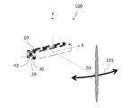
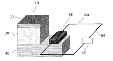
図1は、本開示の例示的な実施形態における光スキャンデバイス100の構成を模式的に示す斜視図である。光スキャンデバイス100は、複数の導波路素子10を含む導波路アレイを備える。複数の導波路素子10の各々は、第1の方向(図1におけるX方向)に延びた形状を有する。複数の導波路素子10は、第1の方向に交差する第2の方向(図1におけるY方向)に規則的に配列されている。複数の導波路素子10は、第1の方向に光を伝搬させながら、第1および第2の方向に平行な仮想的な平面に交差する第3の方向D3に光を出射させる。本実施形態では、第1の方向(X方向)と第2の方向(Y方向)とが直交しているが、両者が直交していなくてもよい。本実施形態では、複数の導波路素子10がY方向に等間隔で並んでいるが、必ずしも等間隔に並んでいる必要はない。
FIG. 1 is a perspective view schematically showing the configuration of an
なお、本願の図面に示される構造物の向きは、説明のわかりやすさを考慮して設定されており、本開示の実施形態が現実に実施されるときの向きをなんら制限するものではない。また、図面に示されている構造物の全体または一部分の形状および大きさも、現実の形状および大きさを制限するものではない。 It should be noted that the orientations of the structures shown in the drawings of the present application are set in consideration of the clarity of explanation, and do not limit the orientations when the embodiments of the present disclosure are actually implemented. Also, the shape and size of all or part of the structures shown in the drawings are not intended to limit the actual shape and size.
複数の導波路素子10のそれぞれは、互いに対向する第1のミラー30および第2のミラー40(以下、それぞれを単に「ミラー」と呼ぶ場合がある)と、ミラー30とミラー40の間に位置する光導波層20とを有する。ミラー30およびミラー40の各々は、第3の方向D3に交差する反射面を、光導波層20との界面に有する。ミラー30およびミラー40、ならびに光導波層20は、第1の方向(X方向)に延びた形状を有している。
Each of the plurality of
なお、後述するように、複数の導波路素子10の複数の第1のミラー30は、一体に構成された第3のミラーの複数の部分であってもよい。また、複数の導波路素子10の複数の第2のミラー40は、一体に構成された第4のミラーの複数の部分であってもよい。さらに、複数の導波路素子10の複数の光導波層20は、一体に構成された光導波層の複数の部分であってもよい。少なくとも、(1)各第1のミラー30が他の第1のミラー30と別体に構成されているか、(2)各第2のミラー40が他の第2のミラー40と別体に構成されているか、(3)各光導波層20が他の光導波層20と別体に構成されていることにより、複数の導波路を形成することができる。「別体に構成されている」とは、物理的に空間を設けることのみならず、間に屈折率が異なる材料を挟み、分離することも含む。
In addition, as will be described later, the plurality of
第1のミラー30の反射面と第2のミラー40の反射面とは略平行に対向している。ミラー30およびミラー40のうち、少なくとも第1のミラー30は、光導波層20を伝搬する光の一部を透過させる特性を有する。言い換えれば、第1のミラー30は、当該光について、第2のミラー40よりも高い光透過率を有する。このため、光導波層20を伝搬する光の一部は、第1のミラー30から外部に出射される。このようなミラー30およびミラー40は、例えば誘電体による多層膜(「多層反射膜」と称することもある。)によって形成される多層膜ミラーであり得る。
The reflective surface of the
それぞれの導波路素子10に入力する光の位相を制御し、さらに、これらの導波路素子10における光導波層20の屈折率もしくは厚さ、または光導波層20に入力される光の波長を同期して同時に変化させることで、光による2次元スキャンを実現することができる。
Control the phase of light input to each
本発明者らは、そのような2次元スキャンを実現するために、導波路素子10の動作原理について詳しく分析を行った。その結果に基づき、複数の導波路素子10を同期して駆動することで、光による2次元スキャンを実現することに成功した。
In order to realize such a two-dimensional scan, the inventors analyzed in detail the principle of operation of the
図1に示されるように、各導波路素子10に光を入力すると、各導波路素子10の出射面から光が出射される。出射面は、第1のミラー30の反射面の反対側に位置する。その出射光の方向D3は、光導波層の屈折率、厚さ、および光の波長に依存する。本実施形態では、各導波路素子10から出射される光が概ね同じ方向になるように、各光導波層の屈折率、厚さ、および波長の少なくとも1つが同期して制御される。これにより、複数の導波路素子10から出射される光の波数ベクトルのX方向の成分を変化させることができる。言い換えれば、出射光の方向D3を、図1に示される方向101に沿って変化させることができる。
As shown in FIG. 1 , when light is input to each
さらに、複数の導波路素子10から出射される光は同じ方向を向いているので、出射光は互いに干渉する。それぞれの導波路素子10から出射される光の位相を制御することにより、干渉によって光が強め合う方向を変化させることができる。例えば、同じサイズの複数の導波路素子10がY方向に等間隔で並んでいる場合、複数の導波路素子10には、一定量ずつ位相の異なる光が入力される。その位相差を変化させることにより、出射光の波数ベクトルの、Y方向の成分を変化させることができる。言い換えれば、複数の導波路素子10に導入される光の位相差をそれぞれ変化させることにより、干渉によって出射光が強め合う方向D3を、図1に示される方向102に沿って変化させることができる。これにより、光による2次元スキャンを実現することができる。
Furthermore, since the lights emitted from the plurality of
以下、光スキャンデバイス100の動作原理をより詳細に説明する。
The operating principle of the
<導波路素子の動作原理>
図2は、1つの導波路素子10の断面の構造および伝搬する光の例を模式的に示す図である。図2では、図1に示すX方向およびY方向に垂直な方向をZ方向とし、導波路素子10のXZ面に平行な断面が模式的に示されている。導波路素子10において、一対のミラー30とミラー40が光導波層20を挟むように配置されている。光導波層20のX方向における一端から導入された光22は、光導波層20の上面(図2における上側の表面)に設けられた第1のミラー30および下面(図2における下側の表面)に設けられた第2のミラー40によって反射を繰り返しながら光導波層20内を伝搬する。第1のミラー30の光透過率は第2のミラー40の光透過率よりも高い。このため、主に第1のミラー30から光の一部を出力することができる。
<Operating Principle of Waveguide Device>
FIG. 2 is a diagram schematically showing a cross-sectional structure of one
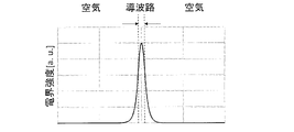
通常の光ファイバーなどの導波路では、全反射を繰り返しながら光が導波路に沿って伝搬する。これに対して、本実施形態における導波路素子10では、光は光導波層20の上下に配置されたミラー30およびミラー40によって反射を繰り返しながら伝搬する。このため、光の伝搬角度に制約がない。ここで光の伝搬角度とは、ミラー30またはミラー40と光導波層20との界面への入射角度を意味する。ミラー30またはミラー40に対して、より垂直に近い角度で入射する光も伝搬できる。すなわち、全反射の臨界角よりも小さい角度で界面に入射する光も伝搬できる。このため、光の伝搬方向における光の群速度は自由空間における光速に比べて大きく低下する。これにより、導波路素子10は、光の波長、光導波層20の厚さ、および光導波層20の屈折率の変化に対して光の伝搬条件が大きく変化するという性質を持つ。このような導波路を、「反射型導波路」または「スローライト導波路」と呼ぶ。
In a waveguide such as an ordinary optical fiber, light propagates along the waveguide while repeating total reflection. On the other hand, in the
導波路素子10の光の伝搬について、より詳しく説明する。光導波層20の屈折率をnw、光導波層20の厚さをdとする。ここで、光導波層20の厚さdは、ミラー30またはミラー40の反射面の法線方向における光導波層20のサイズである。光の干渉条件を考慮すると、波長λの光の伝搬角度θwは、以下の式(1)を満たす。

mはモード次数である。式(1)は、光導波層20内の光が厚さ方向に定在波を形成する条件に相当する。光導波層20内の波長λgがλ/nwのとき、光導波層20の厚さ方向における波長λg’はλ/(nwcosθw)であると考えることができる。光導波層20の厚さdが、光導波層20の厚さ方向における波長λg’の半分λ/(2nwcosθw)の整数倍と等しいとき、定在波が形成される。この条件から式(1)が得られる。なお、式(1)におけるmは定在波の腹(anti-node)の数を表す。
m is the mode order. Equation (1) corresponds to the condition under which the light in the
ミラー30およびミラー40が多層膜ミラーである場合、反射時にミラー内部にも光が侵入する。このため、厳密には、光が侵入した分の光路長に対応する項を式(1)の左辺に付け加える必要がある。しかし、ミラー内部への光の侵入の影響よりも光導波層20の屈折率nwおよび厚さdの影響の方が遥かに大きいため、式(1)によって基本的な動作を説明できる。
If the
光導波層20内を伝搬する光が、第1のミラー30を通じて外部(典型的には空気)に出射されるときの出射角度θは、スネルの法則にしたがって以下の式(2)のように記述できる。

式(2)は、光の出射面において、空気側の光の面方向における波長λ/sinθと、導波路素子10側の光の伝搬方向の波長λ/(nwsinθw)とが等しいという条件から得られる。
Equation (2) states that the wavelength λ/sin θ in the plane direction of the light on the air side is equal to the wavelength λ/(n w sin θ w ) in the propagation direction of the light on the
式(1)および式(2)より、出射角度θは、以下の式(3)のように記述できる。

式(3)からわかるように、光の波長λ、光導波層20の屈折率nwおよび光導波層20の厚さdのいずれかを変えることで光の出射方向を変えることができる。
As can be seen from the equation (3), the light emission direction can be changed by changing any one of the wavelength λ of the light, the refractive index nw of the
例えば、nw=2、d=387nm、λ=1550nm、m=1の場合、出射角度は0°である。この状態から、屈折率をnw=2.2に変化させると、出射角度は約66°に変化する。一方、屈折率を変えずに厚さをd=420nmに変化させると、出射角度は約51°に変化する。屈折率も厚さも変化させずに波長をλ=1500nmに変化させると、出射角度は約30°に変化する。このように、光の波長λ、光導波層20の屈折率nw、および光導波層20の厚さdのいずれかを変えることにより、光の出射方向を大きく変えることができる。
For example, when n w =2, d=387 nm, λ=1550 nm and m=1, the output angle is 0°. From this state, when the refractive index is changed to n w =2.2, the output angle changes to about 66°. On the other hand, if the thickness is changed to d=420 nm without changing the refractive index, the exit angle changes to about 51°. Changing the wavelength to λ=1500 nm without changing the refractive index or the thickness changes the exit angle to about 30°. Thus, by changing any one of the wavelength λ of light, the refractive index n w of the
そこで、本開示の実施形態における光スキャンデバイス100は、光導波層20に入力される光の波長λ、光導波層20の屈折率nw、および光導波層20の厚さdの少なくとも1つを制御することで、光の出射方向を制御する。光の波長λは、動作中に変化させず、一定に維持されてもよい。その場合、よりシンプルな構成で光のスキャンを実現できる。波長λは、特に限定されない。例えば、波長λは、一般的なシリコン(Si)により光を吸収することで光を検出するフォトディテクタまたはイメージセンサで高い検出感度が得られる400nmから1100nm(可視光から近赤外光)の波長域に含まれ得る。他の例では、波長λは、光ファイバーまたはSi導波路において伝送損失の比較的小さい1260nmから1625nmの近赤外光の波長域に含まれ得る。なお、これらの波長範囲は一例である。使用される光の波長域は、可視光または赤外光の波長域に限定されず、例えば紫外光の波長域であってもよい。
Therefore, in the
本発明者らは、上記のような特定方向への光の出射が実際に可能であるかを光学解析によって検証した。光学解析は、サイバネット社のDiffractMODを用いた計算によって行った。これは、厳密結合波解析(RCWA:Rigorous Coupled-Wave Analysis)に基づいたシミュレーションであり、波動光学の効果を正確に計算することができる。 The present inventors verified by optical analysis whether light can actually be emitted in a specific direction as described above. Optical analysis was performed by calculation using Cybernet's DiffractMOD. This is a simulation based on Rigorous Coupled-Wave Analysis (RCWA) and can accurately calculate the effects of wave optics.
図3は、本シミュレーションにおいて用いた計算モデルを模式的に示す図である。この計算モデルでは、基板50上に、第2のミラー40と、光導波層20と、第1のミラー30とが、この順に積層されている。第1のミラー30および第2のミラー40は、いずれも誘電体多層膜を含む多層膜ミラーである。第2のミラー40は、相対的に屈折率の低い低屈折率層42および相対的に屈折率の高い高屈折率層44を交互に6層ずつ(計12層)積層した構造を有する。第1のミラー30は、低屈折率層42および高屈折率層44を交互に2層ずつ(すなわち、計4層)積層した構造を有する。ミラー30とミラー40の間に光導波層20が配置されている。導波路素子10および基板50以外の媒質は空気である。
FIG. 3 is a diagram schematically showing the calculation model used in this simulation. In this calculation model, the
このモデルを用いて、光の入射角度を変化させながら入射光に対する光学応答を調べた。これは、空気からの入射光と光導波層20とが、どの程度結合するかを調べることに対応している。入射光が光導波層20と結合する条件では、光導波層20を伝搬した光が外部に出射されるという逆の過程も起きる。よって、入射光が光導波層20と結合する場合の入射角度を求めることは、光導波層20を伝搬した光が外部に出射する際の出射角度を求めることに相当する。入射光が光導波層20と結合すると、光導波層20内において光の吸収および散乱によるロスが生じる。つまり、大きなロスが生じる条件では、入射光が光導波層20に強く結合しているということになる。吸収などによる光のロスがなければ、光の透過率および反射率の合計が1になる。しかし、ロスがあれば、透過率および反射率の合計は1よりも小さくなる。本計算では、光の吸収の影響を取り入れるために、光導波層20の屈折率に虚部を導入し、1から透過率および反射率の合計を引いた値をロスの大きさとして計算した。
Using this model, we investigated the optical response to incident light while changing the incident angle of the light. This corresponds to examining how incident light from the air and the
本シミュレーションでは、基板50はSi、低屈折率層42はSiO2(厚さ267nm)、高屈折率層44はSi(厚さ108nm)であるものとした。波長λ=1.55μmの光を、角度を様々に変えて入射したときのロスの大きさを計算した。
In this simulation, the
図4Aは、光導波層20の厚さdが704nmの場合における光導波層20の屈折率nwと、モード次数m=1の光の出射角度θとの関係を計算した結果を示している。白い線はロスが大きいことを表している。図4Aに示されているように、nw=2.2付近でモード次数m=1の光の出射角度がθ=0°となる。nw=2.2に近い屈折率をもつ物質には、例えばニオブ酸リチウムがある。
FIG. 4A shows the result of calculating the relationship between the refractive index nw of the
図4Bは、光導波層20の厚さdが446nmの場合における光導波層20の屈折率nwと、モード次数m=1の光の出射角度θとの関係を計算した結果を示している。図4Bに示されているように、nw=3.45付近でモード次数m=1の光の出射角度がθ=0°となる。nw=3.45に近い屈折率をもつ物質には、例えばシリコン(Si)が挙げられる。
FIG. 4B shows the result of calculating the relationship between the refractive index nw of the
このように、光導波層20の厚さdを調整することにより、特定の光導波層20の屈折率nwに対して、特定のモード次数(例えばm=1)の光の出射角度θが0°となるように設計できる。
Thus, by adjusting the thickness d of the
図4Aおよび図4Bに示すように、屈折率の変化に応じて、出射角度θが大きく変わることが確認できた。後述するように、屈折率は、例えばキャリア注入、電気光学効果、および熱光学効果などの様々な方法によって変化させることができる。そのような方法による屈折率の変化は0.1程度とあまり大きくない。そのため、これまでは、そのような小さな屈折率の変化では出射角度はそれほど大きく変化しないと考えられていた。しかし、図4Aおよび図4Bに示すように、出射角度がθ=0°となる屈折率付近では、屈折率が0.1増加すると出射角度θが0°から約30°にまで変化することがわかった。このように、本実施形態における導波路素子10では、小さい屈折率変化であっても、出射角度を大きく調整することが可能である。
As shown in FIGS. 4A and 4B, it has been confirmed that the emission angle θ changes greatly according to the change in the refractive index. As discussed below, the refractive index can be changed by various methods such as carrier injection, electro-optical effects, and thermo-optical effects. The change in refractive index by such a method is not very large, about 0.1. Therefore, until now, it was thought that such a small change in the refractive index would not change the output angle that much. However, as shown in FIGS. 4A and 4B, near the refractive index where the exit angle is θ=0°, the exit angle θ changes from 0° to about 30° when the refractive index increases by 0.1. have understood. Thus, in the
同様に、図4Aおよび図4Bの比較からわかるように、光導波層20の厚さdの変化に応じて、出射角度θが大きく変わることが確認できた。後述するように、厚さdは、例えば2つのミラーの少なくとも一方に接続されたアクチュエータによって変化させることができる。厚さdの変化が小さくても、出射角度を大きく調整することができる。
Similarly, as can be seen from the comparison between FIGS. 4A and 4B, it was confirmed that the emission angle θ varies greatly with changes in the thickness d of the
このように、光導波層20の屈折率nwおよび/または厚さdを変化させることにより、導波路素子10から出射される光の方向を変えることができる。同様に、光導波層20に入力する光の波長を変化させることによっても、導波路素子10から出射される光の方向を変えることができる。出射光の方向を変化させるために、光スキャンデバイス100は、各導波路素子10における光導波層20の屈折率、厚さ、および波長の少なくとも1つを変化させる第1調整素子を備え得る。第1調整素子の構成例については、後述する。
Thus, by changing the refractive index nw and/or the thickness d of the
以上のように、導波路素子10を用いれば、光導波層20の屈折率nw、厚さd、および波長λの少なくとも1つを変化させることで、光の出射方向を大きく変えることができる。これにより、ミラー30から出射される光の出射角度を、導波路素子10に沿った方向に変化させることができる。1つ以上の導波路素子10を用いることにより、このような1次元のスキャンを実現することができる。
As described above, by using the
図5は、単一の導波路素子10によって1次元スキャンを実現する光スキャンデバイス100の例を模式的に示す図である。この例では、Y方向に広がりのあるビームスポットが形成される。光導波層20の屈折率、厚さ、波長の少なくとも1つを変化させることにより、ビームスポットをX方向に沿って移動させることができる。これにより、1次元スキャンが実現される。ビームスポットがY方向に広がりをもつため、一軸方向のスキャンであっても、2次元的に拡がる比較的広いエリアをスキャンすることができる。2次元スキャンが不要な用途では、図5に示すような構成も採用し得る。
FIG. 5 is a diagram schematically showing an example of an
2次元スキャンを実現する場合には、図1に示すように、複数の導波路素子10が配列された導波路アレイが用いられる。複数の導波路素子10内を伝搬する光の位相が特定の条件を満たすとき、光は特定の方向に出射する。その位相の条件が変化すると、光の出射方向が導波路アレイの配列方向にも変化する。すなわち、導波路アレイを用いることにより、2次元スキャンを実現することができる。2次元スキャンを実現するためのより具体的な構成の例については後述する。
To realize two-dimensional scanning, a waveguide array in which a plurality of
以上のように、1つ以上の導波路素子10を用いて、導波路素子10における光導波層20の屈折率、光導波層20の厚さ、および波長の少なくとも1つを変化させることにより、光の出射方向を変化させることができる。本開示の実施形態における導波路素子10は、光の全反射を利用する一般的な全反射導波路とは異なり、光導波層が一対のミラーに挟まれた反射型導波路の構造を備える。このような反射型導波路への光の結合については、これまでに十分に検討されてこなかった。本発明者らは、光導波層20に光を効率的に導入するための構造についても検討した。
As described above, by using one or
図6Aは、空気およびミラー30を介して間接的に光が光導波層20に入力される構成の例を模式的に示す断面図である。この例では、反射型導波路である導波路素子10の光導波層20に対して、外部から空気およびミラー30を介して間接的に伝播光が導入される。光導波層20に光を導入するためには、光導波層20の内部における導波光の反射角θwに対して、スネルの法則(ninsinθin=nwsinθw)を満たす必要がある。ここで、ninは外部媒質の屈折率、θinは伝播光の入射角、nwは光導波層20の屈折率である。この条件を考慮して入射角θinを調整することにより、光の結合効率を最大化することができる。さらに、この例では、第1のミラー30の一部に多層反射膜の膜数を減らした部分が設けられている。その部分から光が入力されることで結合効率を高めることができる。しかし、このような構成では、光導波層20の伝搬定数の変化に起因するθwavの変化に応じて、光導波層20への光の入射角θinを変化させる必要が生じる。
FIG. 6A is a cross-sectional view schematically showing an example of a configuration in which light is indirectly input to the
光導波層20の伝搬定数の変化が生じても、光が常に導波路に結合できる状態を保つために、多層反射膜の膜数を減らした部分に角度広がりのあるビームを入射する方法がある。図6Bは、そのような方法の一例を示している。この例では、導波路素子10に、ミラー30の法線方向に対して角度θinだけ傾けて配置された光ファイバー7から角度広がりのある光が導入される。このような構成によって、外部から空気およびミラー30を介して間接的に光を入射した場合の結合効率について検討する。
Even if the propagation constant of the
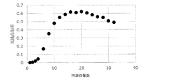
簡単のため光を光線として考える。通常のシングルモードファイバーの開口数(NA)は0.14程度である。これは角度に換算すると約±8度である。導波路に結合する光の入射角度の範囲は、導波路から出射される光の広がり角と同程度である。出射光の広がり角θdivは、以下の式(4)で表される。

ここでLは伝搬長、λは光の波長、θoutは光の出射角である。Lを10μm以上とすると、θdivは大きくても1度以下である。したがって、光ファイバー7からの光の結合効率は、1/16×100%(すなわち、約6.3%)以下である。さらに、光の入射角θinを固定し、導波路の屈折率nwを変化させることによって光の出射角θoutを変化させたときの結合効率の変化を計算した結果を図7に示す。結合効率は、入射光のエネルギーに対する導波光のエネルギーの比を表す。図7に示す結果は、入射角θinを30°、導波路膜厚を1.125μm、波長を1.55μmとして、結合効率を計算することによって得られた。この計算では、屈折率nwを1.44から1.78の範囲で変化させることにより、出射角θoutを10°から65°の範囲で変化させた。図7に示すように、このような構成では、結合効率は最大でも7%に満たない。また、出射角θoutを、結合効率がピークになる出射角から20°以上変化させると、結合効率はさらに半分以下に低下する。
Here, L is the propagation length, λ is the wavelength of light, and θ out is the output angle of light. When L is 10 μm or more, θ div is 1 degree or less at most. Therefore, the coupling efficiency of light from the
このように、光スキャンのために導波路の屈折率等を変化させることによって伝搬定数を変化させると、結合効率はさらに低下する。結合効率を維持するためには、伝搬定数の変化に応じて光の入射角θinを変化させる必要がある。しかし、光の入射角θinを変化させる機構を導入すると、装置構成の複雑化を招く。 In this way, if the propagation constant is changed by changing the refractive index or the like of the waveguide for optical scanning, the coupling efficiency is further reduced. In order to maintain the coupling efficiency, it is necessary to change the incident angle θ in of the light according to the change of the propagation constant. However, introduction of a mechanism for changing the incident angle θ in of light leads to complication of the device configuration.
本発明者らは、屈折率等を変化させる導波路を有する領域の前段に、屈折率が一定に維持される導波路を有する領域を設けることにより、光入射角を固定する事ができることを見出した。さらに、本発明者らは、それらの2種類の導波路を接続して高い光結合効率を実現する方法についても検討した。 The present inventors have found that the light incident angle can be fixed by providing a region having a waveguide whose refractive index is kept constant in front of a region having a waveguide whose refractive index etc. is changed. rice field. Furthermore, the present inventors also studied a method of connecting these two types of waveguides to achieve high optical coupling efficiency.
異なる2つの導波路における導波光の結合を考える際に要因が2点ある。
1つ目は、伝搬光の伝搬定数であり、2つ目はモードの電場強度分布である。これらが2つの導波路において近いほど結合効率は高くなる。導波路における伝搬光の伝搬定数βは、簡単のため幾何光学的に考えると、β=k・sinθw=(2πnwsinθw)/λで表される。波数をk、導波角度をθw、光導波層の屈折率をnwとする。全反射型の導波路では、全反射を用いて導波光を導波層に閉じ込めるため、全反射条件であるnwsinθw>1を満たす。一方、スローライト導波路では、導波路の上下に存在する多層反射膜により光を導波路に閉じ込め、導波光の一部を多層反射膜を通して射出するため、nwsinθw<1となる。全反射型導波路と、導波光の一部を射出するスローライト導波路とでは、伝搬定数は等しくなり得ない。図8Aに示すような全反射導波路の電場強度分布は、図8Bに示すように、ピークを導波路内に持ち、導波路外では単調減少する。他方、図8Cに示すようなスローライト導波路は、図8Dに示すような電場強度分布を持つ。導波路内にピークを持つ事は変わらないが、図8Cに示すスローライト導波路では、導波光が誘電多層膜内において光の干渉により反射する。このため、図8Dに示すように電場強度は誘電多層膜に深く染み出し、かつ振動的に変化する。
There are two factors when considering coupling of guided light in two different waveguides.
The first is the propagation constant of propagating light, and the second is the electric field intensity distribution of the mode. The closer they are in the two waveguides, the higher the coupling efficiency. The propagation constant β of the propagating light in the waveguide is represented by β=k·sin θ w =(2πn w sin θ w )/λ in terms of geometrical optics for simplicity. Let k be the wave number, θ w be the waveguide angle, and n w be the refractive index of the optical waveguide layer. A total reflection waveguide satisfies the condition of total reflection, n w sin θ w >1, since guided light is confined in a waveguide layer using total reflection. On the other hand, in the slow-light waveguide, light is confined in the waveguide by multilayer reflective films present above and below the waveguide, and part of the guided light is emitted through the multilayer reflective film, so n w sin θ w <1. A total reflection waveguide and a slow light waveguide that emits part of the guided light cannot have the same propagation constant. The electric field intensity distribution of the total reflection waveguide as shown in FIG. 8A has a peak inside the waveguide and monotonously decreases outside the waveguide, as shown in FIG. 8B. On the other hand, a slow light waveguide as shown in FIG. 8C has an electric field intensity distribution as shown in FIG. 8D. In the slow-light waveguide shown in FIG. 8C, the guided light is reflected due to light interference in the dielectric multilayer film, although it still has a peak in the waveguide. Therefore, as shown in FIG. 8D, the electric field intensity penetrates deeply into the dielectric multilayer film and vibrates.
以上のように、全反射型導波路とスローライト導波路とでは、導波光の伝搬定数、電場強度分布共に大きく異なる。よって、全反射型導波路とスローライト導波路とを直接的に繋げることは従来考えられていなかった。本発明者らは、可変の屈折率および/または厚さを有する光導波層に、直接的に全反射導波路を繋げることができることを発見した。 As described above, the propagation constant of the guided light and the electric field intensity distribution are significantly different between the total reflection waveguide and the slow light waveguide. Therefore, direct connection between a total reflection waveguide and a slow light waveguide has not been considered in the past. The inventors have discovered that a total internal reflection waveguide can be directly coupled to an optical waveguide layer having a variable refractive index and/or thickness.
さらに、本発明者らは、そのような2種類の導波路を、共通の基板上に配置することにより、光スキャンデバイスの作製を容易にできることも見出した。すなわち、一体に形成された一つの基板上に2種類の導波路を配置してもよい。一般的な導波路は、半導体プロセスを用いて、基板上に作製される。例えば、蒸着またはスパッタリングなどによる成膜と、リソグラフィーまたはエッチングなどによる微細加工とを組み合わせた製法が用いられ得る。そのような製法によって、基板の上に導波路の構造を作製することができる。基板の材料として、例えばSi、SiO2、GaAs、またはGaNが用いられ得る。 Furthermore, the inventors have also found that by arranging such two types of waveguides on a common substrate, fabrication of an optical scanning device can be facilitated. In other words, two types of waveguides may be arranged on one integrated substrate. A typical waveguide is fabricated on a substrate using semiconductor processes. For example, a manufacturing method can be used in which film formation by vapor deposition or sputtering is combined with microfabrication by lithography or etching. Such a manufacturing method can fabricate a waveguide structure on a substrate. Si, SiO 2 , GaAs, or GaN, for example, can be used as substrate material.
反射型導波路も、同様の半導体プロセスを用いて作製され得る。反射型導波路では、光導波層を挟む一対のミラーのうち、一方のミラーから光を透過させることよって、光を出射させる。ミラーは、例えば低コストで入手可能なガラス基板の上に作製され得る。ガラス基板の代わりに、例えばSi、SiO2、GaAs、GaNなどの基板を用いてもよい。 Reflective waveguides can also be made using similar semiconductor processes. In a reflective waveguide, light is emitted by transmitting light through one of a pair of mirrors sandwiching an optical waveguide layer. Mirrors can be fabricated, for example, on glass substrates, which are available at low cost. Substrates such as Si, SiO 2 , GaAs, and GaN may be used instead of the glass substrate.
反射型導波路に別の導波路を接続することによって、光を反射型導波路に導入することができる。以下、そのような構造の例を説明する。 Light can be introduced into the reflective waveguide by connecting another waveguide to the reflective waveguide. Examples of such structures are described below.
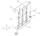
図9は、基板50Aの上に作製された複数の第1の導波路1と、別の基板50Bの上に作製された複数の第2の導波路10との接続を模式的に示す図である。基板50Aおよび基板50Bは、XY平面に平行に配置されている。複数の第1の導波路1および複数の第2の導波路10は、X方向に延び、Y方向に配列されている。第1の導波路1は、例えば、光の全反射を利用する一般的な導波路である。第2の導波路10は、反射型導波路である。別々の基板50Aおよび基板50Bの上にそれぞれ配置された第1の導波路1および第2の導波路10を位置合わせして接続することによって、第1の導波路1から第2の導波路10に光を導入することができる。
FIG. 9 is a diagram schematically showing connections between a plurality of
第1の導波路1から第2の導波路10に効率よく光を導入するためには、10nmオーダーの極めて高精度の位置合わせが望まれる。また、高精度の位置合わせができたとしても、基板50Aおよび基板50Bの熱膨張係数が異なる場合、温度変化により、位置合わせがずれるおそれがある。例えば、Si、SiO2、GaAsおよびGaNの熱膨張係数は、それぞれおよそ4、0.5、6および5(×10―6/K)であり、ガラス基材としてよく使われるBK7の熱膨張係数は、9(×10―6/K)である。別々の基材としてどの材料を組み合わせても、1×10―6/K以上の熱膨張係数の違いが生じる。例えば、複数の第1の導波路1および複数の第2の導波路10の配列方向(図中ではY方向)における基板50Aおよび基板50Bのサイズが1mmである場合、1℃の温度変化によって、基板50Aおよび基板50Bの位置合わせは、1nmずれる。さらに、数十℃の温度変化によって、基板50Aおよび基板50Bの位置合わせは、数十から百nmのオーダーで大きくずれる。
In order to efficiently introduce light from the
同じ基板の上に第1の導波路および第2の導波路を配置すれば、上記の課題を解決できる。共通の基板上にこれらの導波路を配置することにより、第1の導波路および第2の導波路の位置合わせが容易になる。さらに、熱膨張による第1の導波路および第2の導波路の位置合わせのずれが抑制される。その結果、第1の導波路から第2の導波路にさらに効率よく光を導入することができる。 Placing the first waveguide and the second waveguide on the same substrate solves the above problem. Placing these waveguides on a common substrate facilitates alignment of the first waveguide and the second waveguide. Further, misalignment of the first waveguide and the second waveguide due to thermal expansion is suppressed. As a result, light can be more efficiently introduced from the first waveguide to the second waveguide.
上記態様における「第2の導波路」は、前述の実施形態における「導波路素子」に相当する。本開示のある実施形態では、第2の導波路の前段に、屈折率も厚さも一定に維持される第1の導波路が設けられ、第1の導波路に光が入力される。第1の導波路は、入力された光を伝搬させ、第2の導波路の端面から入力する。第1の導波路と第2の導波路とは、端面同士が直接接続されていてもよいし、例えば、端面間にギャップがあってもよい。 The "second waveguide" in the above aspect corresponds to the "waveguide element" in the above-described embodiments. In an embodiment of the present disclosure, a first waveguide having a constant refractive index and a constant thickness is provided in front of the second waveguide, and light is input to the first waveguide. The first waveguide propagates the input light and enters it from the end surface of the second waveguide. The end surfaces of the first waveguide and the second waveguide may be directly connected to each other, or, for example, there may be a gap between the end surfaces.
上記構成によれば、第1の導波路を第2の導波路(すなわち導波路素子)の前段に設けることにより、第1の導波路に入射する光の入射角を一定に維持しても、スキャンによる結合効率の低下(すなわちエネルギーのロス)を抑制することができる。 According to the above configuration, by providing the first waveguide in front of the second waveguide (that is, the waveguide element), even if the incident angle of the light incident on the first waveguide is kept constant, A decrease in coupling efficiency (that is, energy loss) due to scanning can be suppressed.
同じ基板の上に第1の導波路および第2の導波路を配置した場合には、第1の導波路および第2の導波路の位置合わせが容易になる。さらに、熱膨張による第1および第2の導波路の位置合わせのずれが抑制される。その結果、第1の導波路から第2の導波路へ効率よく光を導入することができる。 Placing the first waveguide and the second waveguide on the same substrate facilitates alignment of the first waveguide and the second waveguide. Further, misalignment of the first and second waveguides due to thermal expansion is suppressed. As a result, light can be efficiently introduced from the first waveguide to the second waveguide.
<グレーティングを介した導波光結合>
本発明者らは、図9に示す構成を改良することにより、光の結合効率をさらに向上させることができることを見出した。
<Guided Optical Coupling via Grating>
The inventors have found that the light coupling efficiency can be further improved by improving the configuration shown in FIG.
本開示の第1の項目に係る光デバイスは、実効屈折率がne1である導波モードの光を第1の方向に沿って伝搬させる第1の導波路と、前記第1の方向および前記第1の方向に交差する第2の方向に平行な第1の反射面を有し、前記第1の方向に延びる第1のミラー、前記第1の反射面に対向する第2の反射面を有し、前記第1の方向に延びる第2のミラー、および、前記第1のミラーと前記第2のミラーの間に位置し、空気中の波長がλである光を前記第1の方向に沿って伝搬させる光導波層を備える第2の導波路と、を備える。前記第1の導波路の先端部は、前記光導波層の内部にある。前記第1の反射面に垂直な方向から見て前記第1の導波路および前記第2の導波路が重なる領域において、前記第1の導波路の少なくとも一部および/または前記第2の導波路の少なくとも一部は、前記第1の方向に沿って屈折率が周期的に変化する1つ以上のグレーティングを含む。 An optical device according to a first item of the present disclosure includes: a first waveguide for propagating light in a waveguide mode having an effective refractive index n e1 along a first direction; A first mirror having a first reflecting surface parallel to a second direction crossing the first direction and extending in the first direction, and a second reflecting surface facing the first reflecting surface a second mirror extending in the first direction; and a light having a wavelength in air of λ located between the first mirror and the second mirror for directing light in the first direction. a second waveguide comprising an optical waveguide layer propagating along. The tip of the first waveguide is inside the optical waveguide layer. At least part of the first waveguide and/or the second waveguide in a region where the first waveguide and the second waveguide overlap when viewed from a direction perpendicular to the first reflecting surface includes one or more gratings with periodically varying refractive indices along the first direction.
この光デバイスでは、第1の導波路を伝搬する光は、1つ以上のグレーティングを介して、スローライト導波路である第2の導波路に伝搬することができる。 In this optical device, light propagating in the first waveguide can propagate through one or more gratings to the second waveguide, which is a slow light waveguide.
本開示の第2の項目に係る光デバイスは、第1の項目に係る光デバイスにおいて、前記第1の導波路を伝搬する前記光の導波モードの実効屈折率がne1、前記光の空気中の波長がλであるとき、前記1つ以上のグレーティングの各々の周期が、λ/ne1よりも大きく、λ/(ne1-1)よりも小さい。 The optical device according to the second item of the present disclosure is the optical device according to the first item, wherein the effective refractive index of the waveguide mode of the light propagating in the first waveguide is n e1 , and the light is air The period of each of the one or more gratings is greater than λ/n e1 and less than λ/(n e1 −1), where the wavelength in is λ.
この光デバイスでは、導波光の高い結合効率を実現することができる。 This optical device can achieve high coupling efficiency of guided light.
本開示の第3の項目に係る光デバイスは、第1または第2の項目に係る光デバイスにおいて、前記第1の導波路および前記第2の導波路が重なる前記領域では、前記第1の導波路が、前記第1の反射面に対向する第1の表面、および前記第2の反射面に対向する第2の表面を有する。前記1つ以上のグレーティングの各々は、前記第1の表面および前記第2の表面の少なくとも一方にある。 The optical device according to the third item of the present disclosure is the optical device according to the first or second item, wherein in the region where the first waveguide and the second waveguide overlap, the first waveguide A wave path has a first surface facing the first reflecting surface and a second surface facing the second reflecting surface. Each of the one or more gratings is on at least one of the first surface and the second surface.
この光デバイスでは、導波光の高い結合効率を実現することができる。 This optical device can achieve high coupling efficiency of guided light.
本開示の第4の項目に係る光デバイスは、第1から第3の項目のいずれかに係る光デバイスにおいて、前記1つ以上のグレーティングの各々が、前記第1の反射面および前記第2の反射面の少なくとも一方にある。 An optical device according to a fourth item of the present disclosure is the optical device according to any one of the first to third items, wherein each of the one or more gratings includes the first reflecting surface and the second reflecting surface. on at least one of the reflective surfaces.
この光デバイスでは、導波光の高い結合効率を実現することができる。 This optical device can achieve high coupling efficiency of guided light.
本開示の第5の項目に係る光デバイスは、第1から第4の項目のいずれかに係る光デバイスにおいて、前記1つ以上のグレーティングの各々が、前記第1の方向に沿って並ぶ複数の凹部または凸部を含む。前記複数の凹部または凸部の個数は、4以上である。 An optical device according to a fifth item of the present disclosure is the optical device according to any one of the first to fourth items, wherein each of the one or more gratings is arranged along the first direction. Including recesses or protrusions. The number of the plurality of concave portions or convex portions is four or more.
この光デバイスでは、導波光の高い結合効率を実現することができる。 This optical device can achieve high coupling efficiency of guided light.
本開示の第6の項目に係る光デバイスは、第5の項目に係る光デバイスにおいて、前記複数の凹部または凸部の個数が、4以上64以下である。 An optical device according to a sixth item of the present disclosure is the optical device according to the fifth item, wherein the number of the plurality of concave portions or convex portions is 4 or more and 64 or less.
この光デバイスでは、導波光の高い結合効率を実現することができる。 This optical device can achieve high coupling efficiency of guided light.
本開示の第7の項目に係る光デバイスは、第1から第6の項目のいずれかに係る光デバイスにおいて、前記1つ以上のグレーティングの各々は、前記第1の方向に沿って並ぶ複数の凹部を含む。各凹部の深さは、前記第1の導波路の厚さの3分の1以上15分の8以下である。 The optical device according to a seventh item of the present disclosure is the optical device according to any one of the first to sixth items, wherein each of the one or more gratings is a plurality of gratings arranged along the first direction. Including recesses. The depth of each recess is ⅓ or more and 8/15 or less of the thickness of the first waveguide.
この光デバイスでは、導波光の高い結合効率を実現することができる。 This optical device can achieve high coupling efficiency of guided light.
本開示の第8の項目に係る光デバイスは、第1から第7の項目のいずれかに係る光デバイスにおいて、前記1つ以上のグレーティングが、複数のグレーティングである。前記複数のグレーティングの周期は互いに異なる。 An optical device according to an eighth item of the present disclosure is the optical device according to any one of the first to seventh items, wherein the one or more gratings are a plurality of gratings. The periods of the plurality of gratings are different from each other.
この光デバイスでは、第1の導波路を伝搬する光は、互いに周期が異なる複数のグレーティングを介して、スローライト導波路である第2の導波路に高い効率で伝搬することができる。これにより、製造誤差に起因する結合効率の低下を抑制することができる。 In this optical device, light propagating through the first waveguide can be propagated with high efficiency to the second waveguide, which is a slow light waveguide, via a plurality of gratings with different periods. As a result, it is possible to suppress a decrease in coupling efficiency due to manufacturing errors.
第9の項目に係る光デバイスは、第8の項目に係る光デバイスにおいて、前記複数のグレーティングが、前記第1の方向に沿って並ぶ2つ以上のグレーティングを含む。 The optical device according to the ninth item is the optical device according to the eighth item, wherein the plurality of gratings includes two or more gratings arranged along the first direction.
この光デバイスでは、導波光の高い結合効率を実現することができる。 This optical device can achieve high coupling efficiency of guided light.
第10の項目に係る光デバイスは、第8または第9の項目に係る光デバイスにおいて、前記複数のグレーティングが、前記第2の方向において隣接する2つ以上のグレーティングを含む。 The optical device according to the tenth item is the optical device according to the eighth or ninth item, wherein the plurality of gratings includes two or more gratings adjacent in the second direction.
この光デバイスでは、導波光の高い結合効率を実現することができる。 This optical device can achieve high coupling efficiency of guided light.
第11の項目に係る光デバイスは、光を第1の方向に沿って伝搬させる第1の導波路と、前記第1の方向および前記第1の方向に交差する第2の方向に平行な第1の反射面を有し、前記第1の方向に延びる第1のミラー、前記第1の反射面に対向する第2の反射面を有し、前記第1の方向に延びる第2のミラー、および、前記第1のミラーと前記第2のミラーの間に位置し、前記光を前記第1の方向に沿って伝搬させる光導波層を備える第2の導波路と、を備える。前記第1の導波路の先端部は、前記光導波層の内部にある。前記第1の反射面に垂直な方向から見て前記第1の導波路および前記第2の導波路が重なる領域において、前記第1の導波路の少なくとも一部および/または前記第2の導波路の少なくとも一部は、前記第1の方向に沿って屈折率が変化するグレーティングを含み、前記グレーティングは、複数の周期成分を含む。 The optical device according to the eleventh item includes a first waveguide for propagating light along a first direction, and a second waveguide parallel to the first direction and a second direction intersecting the first direction. a first mirror having one reflecting surface and extending in the first direction; a second mirror having a second reflecting surface facing the first reflecting surface and extending in the first direction; and a second waveguide located between the first mirror and the second mirror and comprising an optical waveguide layer for propagating the light along the first direction. The tip of the first waveguide is inside the optical waveguide layer. At least part of the first waveguide and/or the second waveguide in a region where the first waveguide and the second waveguide overlap when viewed from a direction perpendicular to the first reflecting surface includes a grating with a refractive index that varies along the first direction, the grating including a plurality of periodic components .
この光デバイスでは、第1の導波路を伝搬する光は、複数の周期成分を含むグレーティングを介して、スローライト導波路である第2の導波路に伝搬することができる。 In this optical device, light propagating through the first waveguide can propagate to the second waveguide, which is a slow light waveguide, via the grating including a plurality of periodic components.
第12の項目に係る光デバイスは、第11の項目に係る光デバイスにおいて、前記第1の導波路を伝搬する前記光の導波モードの実効屈折率がne1、前記光の空気中の波長がλであるとき、前記複数の周期成分の各々の周期が、λ/ne1よりも大きく、λ/(ne1-1)よりも小さい。 The optical device according to the twelfth item is the optical device according to the eleventh item, wherein the effective refractive index of the waveguide mode of the light propagating in the first waveguide is n e1 , and the wavelength of the light in air is λ, the period of each of the plurality of periodic components is larger than λ/n e1 and smaller than λ/(n e1 −1).
この光デバイスでは、導波光の高い結合効率を実現することができる。 This optical device can achieve high coupling efficiency of guided light.
本開示の第13の項目に係る光デバイスは、第1から第12の項目のいずれかに係る光デバイスにおいて、前記第1のミラーと前記第2のミラーに挟まれた2つの非導波領域であって、前記光導波層が間にある2つの非導波領域をさらに備える。前記光導波層の平均屈折率は、各非導波領域の平均屈折率よりも高い。 An optical device according to a thirteenth item of the present disclosure is the optical device according to any one of the first to twelfth items, wherein two non-guiding regions sandwiched between the first mirror and the second mirror are provided. and further comprising two non-guiding regions between which the optical guiding layer is located. The average refractive index of the optical waveguide layer is higher than the average refractive index of each non-guiding region.
この光デバイスでは、光は、各非導波領域に漏れることなく、第2の導波路における光導波層内を伝搬することができる。 In this optical device, light can propagate through the optical waveguide layer in the second waveguide without leaking into each non-guiding region.
本開示の第14の項目に係る光デバイスは、第13の項目に係る光デバイスにおいて、前記2つの非導波領域の各々が、屈折率が異なる2つ以上の部材を含む。 An optical device according to a fourteenth item of the present disclosure is the optical device according to the thirteenth item, wherein each of the two non-guiding regions includes two or more members having different refractive indices.
この光デバイスでは、第11の項目に係る光デバイスと同じ効果を得ることができる。 With this optical device, the same effects as those of the optical device according to the eleventh item can be obtained.
本開示の第15の項目に係る光デバイスは、第13または第14の項目に係る光デバイスにおいて、前記光導波層および前記2つの非導波領域が、共通の材料によって構成される領域を含む。 The optical device according to the fifteenth item of the present disclosure is the optical device according to the thirteenth or fourteenth item, wherein the optical waveguide layer and the two non-guiding regions include regions made of a common material. .
この光デバイスでは、共通の材料にコストの安い材料を用いることによって製造コストを下げることができる。 In this optical device, the manufacturing cost can be reduced by using inexpensive materials as common materials.
本開示の第16の項目に係る光デバイスは、第1から第15の項目のいずれかに係る光デバイスにおいて、前記第1の導波路を支持する誘電体層をさらに備る。前記第2のミラーは前記誘電体層を支持する。 An optical device according to a sixteenth item of the present disclosure is the optical device according to any one of the first to fifteenth items, further comprising a dielectric layer supporting the first waveguide. The second mirror supports the dielectric layer.
この光デバイスでは、第2のミラーが、第1の導波路および第2の導波路の共通の基板として用いられ、第1の導波路が、誘電体層によって支持されている。これにより、光デバイスの作製が容易になる。 In this optical device, a second mirror is used as a common substrate for the first waveguide and the second waveguide, the first waveguide being supported by a dielectric layer. This facilitates fabrication of optical devices.
本開示の第17の項目に係る光デバイスは、第16の項目に係る光デバイスにおいて、前記光導波層の内部では、前記誘電体層の前記第2の方向における幅が、前記光導波層の前記第2の方向における幅と同一である。 The optical device according to a seventeenth item of the present disclosure is the optical device according to the sixteenth item, wherein inside the optical waveguide layer, the width of the dielectric layer in the second direction is equal to the width of the optical waveguide layer. It is the same as the width in the second direction.
この光デバイスでは、光散乱ロスを抑制することができる。 This optical device can suppress light scattering loss.
本開示の第18の項目に係る光デバイスは、第17の項目に係る光デバイスにおいて、前記光導波層の内部では、前記第1の導波路の前記第2の方向における幅が、前記誘電体層の前記第2の方向における幅よりも狭い。 An optical device according to an eighteenth item of the present disclosure is the optical device according to the seventeenth item, wherein inside the optical waveguide layer, the width of the first waveguide in the second direction is equal to the dielectric It is narrower than the width of the layer in said second direction.
この光デバイスでは、光散乱ロスを抑制することができる。 This optical device can suppress light scattering loss.
本開示の第19の項目に係る光デバイスは、第17の項目に係る光デバイスにおいて、前記光導波層の内部では、前記第1の導波路の前記第2の方向における幅が、前記誘電体層の前記第2の方向における幅と同一である。 The optical device according to a nineteenth item of the present disclosure is the optical device according to the seventeenth item, wherein inside the optical waveguide layer, the width of the first waveguide in the second direction is equal to the dielectric It is the same as the width of the layer in said second direction.
この光デバイスでは、光散乱ロスを抑制することができる。 This optical device can suppress light scattering loss.
本開示の第20の項目に係る光デバイスは、第1から第19の項目のいずれかに係る光デバイスにおいて、前記光導波層の外部では、前記第1の導波路が、前記第2の導波路に近づくにつれて、前記第2の方向の幅が単調に増加する部分を含む。 An optical device according to a twentieth item of the present disclosure is the optical device according to any one of the first to nineteenth items, wherein outside the optical waveguide layer, the first waveguide is the second waveguide. It includes a portion in which the width in the second direction monotonically increases as it approaches the wave path.
この光デバイスでは、光導波層の外部において、第1の導波路は、テーパー構造を備える。第1の導波路において、光は、幅の狭い導波路から、テーパー構造を介して幅の広い導波路に入射する。テーパー構造により、幅の広い導波路に入射する光の反射が抑制される。 In this optical device, the first waveguide has a tapered structure outside the optical waveguide layer. In the first waveguide, light enters the wide waveguide from the narrow waveguide through the tapered structure. The tapered structure suppresses reflection of light incident on the wide waveguide.
本開示の第21の項目に係る光デバイスは、第1から第20の項目のいずれかに係る光デバイスにおいて、前記第1のミラーが、前記第2のミラーよりも高い光透過率を有し、前記光導波層を伝搬する前記光の一部を、前記第1の反射面に交差する第3の方向に出射する。 An optical device according to a twenty-first item of the present disclosure is the optical device according to any one of the first to twentieth items, wherein the first mirror has a higher light transmittance than the second mirror, , a portion of the light propagating through the optical waveguide layer is emitted in a third direction intersecting the first reflecting surface.
この光デバイスでは、第2の導波路における光導波層を伝搬する光は、第1のミラーから外部に出射される。 In this optical device, light propagating through the optical waveguide layer in the second waveguide is emitted outside through the first mirror.
本開示の第22の項目に係る光デバイスは、第1から第20の項目のいずれかに係る光デバイスにおいて、前記第1のミラーが、前記第2のミラーよりも高い光透過率を有する。前記光導波層は、前記第1の反射面に交差する第3の方向から前記第1のミラーを介して前記光導波層に入射した光を前記第1の方向に沿って伝搬させる。 An optical device according to a twenty-second item of the present disclosure is the optical device according to any one of the first to twentieth items, wherein the first mirror has a higher light transmittance than the second mirror. The optical waveguide layer propagates light incident on the optical waveguide layer via the first mirror from a third direction intersecting the first reflecting surface along the first direction.
この光デバイスでは、外部から入射する光を、第1のミラーを介して第2の導波路における光導波層に伝搬させることができる。 In this optical device, externally incident light can be propagated through the first mirror to the optical waveguide layer in the second waveguide.
本開示の第23の項目に係る光デバイスは、第21または第22の項目に係る光デバイスにおいて、前記光導波層の少なくとも一部が、屈折率および/または厚さを調整することが可能な構造を有する。前記屈折率および/または前記厚さを調整することにより、前記第3の方向が変化する。 The optical device according to the twenty-third item of the present disclosure is the optical device according to the twenty-first or twenty-second item, wherein at least part of the optical waveguide layer is capable of adjusting the refractive index and/or thickness have a structure. The third direction is varied by adjusting the refractive index and/or the thickness.
この光デバイスでは、前記屈折率および/または前記厚さを調整することにより、第21の項目に係る光デバイスから出射される光の方向、または、第22の項目に係る光デバイスが受信する光の方向を変化させることができる。
In this optical device, the direction of light emitted from the optical device according to item 21 or the light received by the optical device according to
本開示の第24の項目に係る光デバイスは、第23の項目に係る光デバイスにおいて、前記光導波層の前記少なくとも一部を間に挟む一対の電極と、前記一対の電極に電圧を印加することにより、前記光導波層の前記少なくとも一部の屈折率を変化させる制御回路と、をさらに備える。前記光導波層の前記少なくとも一部は、液晶材料または電気光学材料を含む。 An optical device according to a twenty-fourth item of the present disclosure is the optical device according to the twenty-third item, wherein a voltage is applied to a pair of electrodes sandwiching the at least part of the optical waveguide layer, and to the pair of electrodes. and a control circuit for changing the refractive index of the at least part of the optical waveguide layer. Said at least part of said optical waveguide layer comprises a liquid crystal material or an electro-optical material.
この光デバイスでは、光導波層の少なくとも一部は、液晶材料または電気光学材料を含む。光導波層の上記少なくとも一部を一対の電極で挟み、電圧を印加することにより、第23の項目に係る光デバイスの効果を実現することができる。 In this optical device, at least part of the optical waveguide layer includes a liquid crystal material or an electro-optic material. By sandwiching at least part of the optical waveguide layer between a pair of electrodes and applying a voltage, the effect of the optical device according to the 23rd item can be realized.
本開示の第25の項目に係る光デバイスは、第24の項目に係る光デバイスにおいて、前記一対の電極が、前記光導波層のうち、前記第1の反射面に垂直な方向から見て前記第1の導波路に重なる部分とは異なる部分を間に挟む。 The optical device according to a twenty-fifth item of the present disclosure is the optical device according to the twenty-fourth item, wherein the pair of electrodes of the optical waveguide layer has the A portion different from the portion overlapping the first waveguide is interposed therebetween.
この光デバイスでは、光導波層のうち、第1の導波路と重なる部分とは異なる部分に電圧を印加することができる。 In this optical device, a voltage can be applied to a portion of the optical waveguide layer that is different from the portion overlapping the first waveguide.
本開示の第26の項目に係る光デバイスは、第25の項目に係る光デバイスにおいて、前記一対の電極は第1の一対の電極であり、前記光導波層のうち、前記第1の反射面に垂直な方向から見て前記第1の導波路に重なる部分の少なくとも一部を間に挟む第2の一対の電極をさらに備える。前記制御回路は、前記第1の一対の電極および前記第2の一対の電極に独立して電圧を印加することにより、前記第1の一対の電極の間に位置する前記光導波層の部分の屈折率と、前記第2の一対の電極に挟まれた前記光導波層の部分の屈折率とを独立して調整する。 An optical device according to a twenty-sixth item of the present disclosure is the optical device according to the twenty-fifth item, wherein the pair of electrodes is a first pair of electrodes, and the optical waveguide layer includes and a second pair of electrodes sandwiching at least a portion of the portion overlapping with the first waveguide when viewed in a direction perpendicular to the direction of the waveguide. The control circuit independently applies voltages to the first pair of electrodes and the second pair of electrodes to control the portion of the optical waveguide layer positioned between the first pair of electrodes. The refractive index and the refractive index of the portion of the optical waveguide layer sandwiched between the second pair of electrodes are independently adjusted.
この光デバイスでは、光導波層のうち、第1の導波路と重なる部分の少なくとも一部と、それ以外の部分の少なくとも一部とに独立して電圧を印加することができる。これにより、光導波層のうち、第1の導波路と重なる部分の少なくとも一部の屈折率と、それ以外の部分の少なくとも一部の屈折率とを独立して調整することができる。 In this optical device, a voltage can be applied independently to at least a portion of the optical waveguide layer overlapping with the first waveguide and at least a portion of the other portion. This makes it possible to independently adjust the refractive index of at least a portion of the optical waveguide layer overlapping with the first waveguide and the refractive index of at least a portion of the other portion.
本開示の第27の項目に係る光デバイスは、第23の項目に係る光デバイスにおいて、前記第1のミラーおよび前記第2のミラーの少なくとも一方に接続された1つ以上のアクチュエータと、前記1つ以上のアクチュエータを制御して前記第1のミラーと前記第2のミラーとの距離を変化させることにより、前記光導波層の厚さを変化させる制御回路と、
をさらに備える。
The optical device according to the twenty-seventh item of the present disclosure is the optical device according to the twenty-third item, wherein one or more actuators connected to at least one of the first mirror and the second mirror; a control circuit for changing the thickness of the optical waveguide layer by controlling one or more actuators to change the distance between the first mirror and the second mirror;
further provide.
この光デバイスでは、1つ以上のアクチュエータは、第1のミラーおよび第2のミラーの少なくとも一方に接続されている。1つ以上のアクチュエータを制御して第1のミラーと第2のミラーとの距離を変化させることにより、第23の項目に係る光デバイスの効果を実現することができる。 In this optical device, one or more actuators are connected to at least one of the first mirror and the second mirror. By controlling one or more actuators to change the distance between the first mirror and the second mirror, the effect of the optical device according to the twenty-third item can be realized.
本開示の第28の項目に係る光デバイスは、第1から第27の項目のいずれかに係る光デバイスにおいて、各々が、前記第1の導波路と、前記第2の導波路とを含む複数の導波路ユニットをさらに備える。前記複数の導波路ユニットは、前記第2の方向に配列されている。 The optical device according to the twenty-eighth item of the present disclosure is the optical device according to any one of the first to twenty-seventh items, each of which includes a plurality of waveguides each including the first waveguide and the second waveguide. waveguide unit. The plurality of waveguide units are arranged in the second direction.
この光デバイスでは、複数の導波路ユニットがアレイ化されている。複数の導波路ユニットの各々は、第1の導波路と、前記第2の導波路とを含む。これにより、2次元におけるスキャンおよび光受信を実現することができる。 In this optical device, a plurality of waveguide units are arrayed. Each of the plurality of waveguide units includes a first waveguide and the second waveguide. This makes it possible to realize scanning and optical reception in two dimensions.
本開示の第29の項目に係る光デバイスは、第21から第27の項目のいずれかに係る光デバイスにおいて、各々が、前記第1の導波路と、前記第2の導波路とを含む複数の導波路ユニットをさらに備える。前記複数の導波路ユニットは、前記第2の方向に配列されている。前記複数の導波路ユニットにそれぞれ接続された複数の位相シフタであって、それぞれが、前記複数の導波路ユニットの対応する1つにおける前記第1の導波路に直接的にまたは他の導波路を介して繋がる導波路を含む複数の位相シフタをさらに備える。前記複数の位相シフタを通過する光の位相の差をそれぞれ変化させることにより、前記第3の方向が変化する。 The optical device according to the twenty-ninth item of the present disclosure is the optical device according to any one of the twenty-first to twenty-seventh items, each of which includes a plurality of waveguides each including the first waveguide and the second waveguide waveguide unit. The plurality of waveguide units are arranged in the second direction. a plurality of phase shifters respectively connected to the plurality of waveguide units, each directly to the first waveguide or to the other waveguide in a corresponding one of the plurality of waveguide units; It further comprises a plurality of phase shifters including waveguides leading therethrough. The third direction is changed by changing the phase difference of the light passing through the plurality of phase shifters.
この光デバイスでは、位相シフタによって光スキャンおよび光受信の方向を変化させることができる。 In this optical device, the direction of optical scanning and optical reception can be changed by a phase shifter.
本開示の第30の項目に係る光検出システムは、第1から第29の項目のいずれかに記載の光デバイスと、前記光デバイスから出射され、対象物から反射された光を検出する光検出器と、前記光検出器の出力に基づいて、距離分布データを生成する信号処理回路と、を備える。 A photodetection system according to a thirtieth item of the present disclosure includes the optical device according to any one of the first to twenty-ninth items, and a photodetector that detects light emitted from the optical device and reflected from an object and a signal processing circuit that generates distance distribution data based on the output of the photodetector.
この光検出システムでは、対象物から反射された光が戻ってくる時間を計測することにより、対象物の距離分布データを得ることができる。 In this photodetection system, the distance distribution data of the object can be obtained by measuring the time it takes for the light reflected from the object to return.
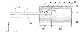
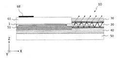
図10は、本開示の例示的な実施形態における光デバイスを模式的に示す断面図である。本実施形態および後述する本実施形態の変形例の全反射導波路1およびスローライト導波路10は、本開示の何れ光デバイスに適用してもよい。
FIG. 10 is a cross-sectional view that schematically illustrates an optical device in an exemplary embodiment of the present disclosure; The
本実施形態では、全反射導波路である第1の導波路1の先端部は、スローライト導波路である第2の導波路10における光導波層20の内部にある。以下、第1の導波路1を「全反射導波路1」と称し、第2の導波路10を「スローライト導波路10」と称することがある。Z方向からみたとき、全反射導波路1およびスローライト導波路10が重なる領域101において、全反射導波路1は、X方向に沿って屈折率が周期pで変化するグレーティング15を備える。図10に示すグレーティング15は、X方向に並ぶ複数の凹部を有する。図10には4つの凹部が例示されているが、実際にはさらに多数の凹部が設けられ得る。複数の凹部に代えて、複数の凸部が設けられていてもよい。グレーティング15におけるX方向に並ぶ凹部または凸部の個数は、例えば4以上が望ましい。また、凹部または凸部の個数は、4以上64以下であり得る。ある例では、凹部または凸部の個数は、8以上32以下であり得る。ある例では、凹部または凸部の個数は、8以上16以下であり得る。凹部または凸部の個数は、各凹部または凸部の回折効率に応じて調整され得る。各凹部または凸部の回折効率は、その深さまたは高さ、および幅などの寸法条件に依存する。したがって、グレーティング15全体として良好な特性が得られるように、各凹部または凸部の寸法に応じて、それらの個数は調整される。
In this embodiment, the tip of the
全反射導波路1は、領域101において、ミラー30の反射面に対向する第1の表面1s1、およびミラー40の反射面に対向する第2の表面1s2を有する。図10に示す例では、グレーティング15は、全反射導波路1の第1の表面1s1に設けられている。グレーティング15は、第2の表面1s2に設けられていてもよい。グレーティング15は、全反射導波路1の第1の表面1s1および第2の表面1s2の少なくとも一方に設けられ得る。
Total
グレーティング15は、全反射導波路1とスローライト導波路10との界面に限らず、他の位置に設けられていてもよい。また、複数のグレーティングが設けられていてもよい。ミラー30の反射面に垂直な方向から見て導波路1および導波路10が重なる領域101において、導波路1および導波路10の少なくとも一部は、1つ以上のグレーティングを含み得る。各グレーティングは、導波路1および導波路10が延びるX方向に沿って屈折率が周期的に変化する。
The grating 15 may be provided not only at the interface between the
全反射導波路1のうち、光導波層20の外部に位置する部分は、他の誘電体層によって支持されてもよいし、2つの誘電体層によって挟まれていてもよい。
A portion of the
領域101のX方向における寸法は、例えば、4μmから50μm程度であり得る。そのような大きさの領域101の内部に、8周期から32周期程度のグレーティング15が形成され得る。スローライト導波路10のうち領域101以外の領域102のX方向における寸法は、例えば、100μmから5mm程度であり得る。領域101のX方向における寸法は、例えば領域102の寸法の数百分の1から数十分の1程度であり得る。ただし、この寸法に限定されず、必要な特性に応じて各部材の寸法は決定される。
The dimension in the X direction of the
領域101において、第1のミラー30は、第2のミラー40よりも高い透過率を有していなくてもよい。領域102においても、領域101に近い領域では、第1のミラー30は、第2のミラー40よりも高い透過率を有していなくてもよい。領域101は、光の結合効率を高めるために設けられる。このため、領域101の近傍では、スローライト導波路10は、必ずしも光を出射する必要はない。
In
全反射導波路1における導波モードの伝搬定数をβ1=2πne1/λとし、スローライト導波路10における導波モードの伝搬定数をβ2=2πne2/λとする。λは、空気中における光の波長である。ne1およびne2は、それぞれ全反射導波路1およびスローライト導波路10における実効屈折率(等価屈折率とも称する)である。全反射導波路1内を伝搬する光は、外部の空気とは結合しない。そのような導波モードの実効屈折率は、ne1>1である。一方、スローライト導波路10における光導波層20を伝搬する光の一部は、外部の空気に出射される。そのような導波モードの実効屈折率は、0<ne2<1である。したがって、β1とβ2とは大きく異なる。そのため、一般に、全反射導波路1からスローライト導波路10への導波光の結合効率は低い。
Let the propagation constant of the guided mode in the
領域101において、全反射導波路1がグレーティング15を備える場合、グレーティング15に起因する回折が生じる。その場合、全反射導波路1における導波モードの伝搬定数β1は、逆格子2π/pの整数倍だけシフトする。例えば-1次回折によってβ1がβ1-(2π/p)にシフトする場合、pを適切に設定すれば、β1-(2π/p)=β2が成り立つようにすることができる。その場合、領域101における2つの伝搬定数が一致するため、導波光は全反射導波路1からスローライト導波路10に高い効率で結合する。β1-(2π/p)=β2から、周期pは以下の式(5)によって表される。

0<ne2<1であるため、周期pは、以下の式(6)を満たす。

スローライト導波路10において、領域101と、それ以外の領域102とでは、同じ導波モードであることから、導波光は高い効率で結合する。
In the
図11は、グレーティングを介した全反射導波路からスローライト導波路に光を伝搬させたときの電場分布の計算例を示す図である。計算には、Synopsys社のModePROPを用いた。図11に示すように、全反射導波路1を伝搬する光は、グレーティング15を介してスローライト導波路10に効率よく伝搬する。
FIG. 11 is a diagram showing a calculation example of an electric field distribution when light propagates from a total reflection waveguide through a grating to a slow light waveguide. ModePROP from Synopsys was used for the calculation. As shown in FIG. 11, the light propagating through the
図11に示す例における計算条件は、以下の通りである。 The calculation conditions in the example shown in FIG. 11 are as follows.
全反射導波路1において、屈折率はnw1=1.88であり、Z方向の厚さはd1=300nmである。スローライト導波路10において、屈折率はnw2=1.6であり、Z方向の厚さはd2=2.1μmである。グレーティングにおける凹部の数は16である。グレーティングの周期はp=800nmである。各凹部の深さは200nmである。全反射導波路1およびスローライト導波路10を伝搬する光は、空気中において波長λ=940nmを有する。全反射導波路1における伝搬モードの光の実効屈折率ne1は1.69であり、領域101におけるスローライト導波路10における伝搬モードの光の実効屈折率ne2は0.528であった。
In the total
この例では、全反射導波路1からスローライト導波路10への導波光の結合効率は、61.4%であった。グレーティング15が存在しない構成、および全反射導波路1の端面とスローライト導波路10の端面とが直接接続された構成と比較して、結合効率が大幅に向上することが確認された。
In this example, the coupling efficiency of guided light from the
比較のため、図12に示すように、グレーティングが存在しない構成においても同様の計算を行った。計算条件は、グレーティングが存在しないことを除けば、上記の条件と同じである。この場合、結合効率は1.8%であった。また、全反射導波路1の端面とスローライト導波路10の端面とが直接接続された構成においても、結合効率が例えば数%程度に留まることが確認されている。
For comparison, similar calculations were also performed for a configuration without a grating, as shown in FIG. The calculation conditions are the same as above except that no grating is present. In this case the coupling efficiency was 1.8%. Further, it has been confirmed that even in a configuration in which the end face of the
次に、全反射導波路1および導波路10における導波モードを説明する。
Next, waveguide modes in the
図13Aは、全反射導波路1における導波モードの電場強度分布の例を示す図である。図13Bは、スローライト導波路10における高次の導波モードの電場強度分布の例を示す図である。図13Aおよび図13Bに示す例では、YZ平面における電界強度分布が示されている。図13Bに示す例では、第1のミラー30と第2のミラー40との間において、光導波層20は、2つの非導波領域73の間にある。
FIG. 13A is a diagram showing an example of the electric field intensity distribution of the waveguide mode in the
図13Aに示す全反射導波路1における導波モードはシングルモードである。図13Bに示すスローライト導波路10における導波モードは、式(3)におけるm=7の高次モードである。全反射導波路1における実効屈折率はne1=1.69であり、スローライト導波路10における実効屈折率はne2=0.528である。
The waveguide mode in the
図13Aおよび図13Bに示すように導波モードの分布が大きく異なっていても、グレーティング15を介すことにより、導波光の結合効率は高くなる。
As shown in FIGS. 13A and 13B, even if the waveguide mode distributions are significantly different, the coupling efficiency of the guided light is increased through the
スローライト導波路10における高次モードには、以下の利点がある。スローライト導波路10では、全体の電界強度分布に対する光導波層20での電界強度分布の占める比率は、高次モードの方が、低次モードよりも高い。すなわち、高次モードでは、光導波層20に閉じ込められる光の量がより多い。そのため、光導波層20の屈折率の変化に対して、スローライト導波路10から出射される光の出射角度は大きく変化する。
Higher order modes in the
当然、スローライト導波路10における導波モードは、式(3)におけるm=7の高次モードに限定されない。式(5)におけるpを調整することにより、スローライト導波路10において他の導波モードを励起させることも可能である。
Naturally, the waveguide mode in the
図10および図11に示す例において、領域101における全反射導波路1と各ミラーとの距離が近ければ、以下の現象が生じ得る。第1のミラー30および/または第2のミラー40が全反射導波路1よりも高い屈折率を有する場合、全反射導波路1におけるエバネッセント光は、第1のミラー30および/または第2のミラー40に移る傾向にある。その結果、全反射導波路1を伝搬する光は、第1のミラー30および/または第2のミラー40を介して外部に漏れ得る。そのため、領域101における全反射導波路1と各ミラーとの距離は、λ/4以上離れている。これにより、全反射導波路1からスローライト導波路10への導波光の結合効率の低下を抑制できる。
In the examples shown in FIGS. 10 and 11, if the distance between the
図14は、グレーティング15における各凹部の深さと、導波光の結合効率との関係の例を示す図である。この例では、光の波長は940nmである。全反射導波路1の屈折率nw1は1.88である。全反射導波路1の厚さd1は300nmである。スローライト導波路10の屈折率nw2は1.68である。スローライト導波路の厚さd2は2.1μmである。グレーティング15の周期pは800nmである。グレーティング15における凹部の数は32である。
FIG. 14 is a diagram showing an example of the relationship between the depth of each recess in the grating 15 and the coupling efficiency of guided light. In this example, the wavelength of light is 940 nm. The refractive index nw1 of the
図14に示す例では、結合効率は、凹部の深さが0から0.13μmの範囲では、当該深さの増加とともに単調に増加する。凹部の深さが0.13μmよりも大きい範囲では、凹部の深さを増加させると、結合効率が低下し、その後振動する。 In the example shown in FIG. 14, the coupling efficiency increases monotonically with increasing recess depth in the range of 0 to 0.13 μm. In the range where the depth of the recess is greater than 0.13 μm, increasing the depth of the recess reduces the coupling efficiency and then oscillates.
図14に示す例では、凹部の深さが0.13μmのとき、結合効率は約50%になり、最大になる。この例では、グレーティング15における各凹部の深さが、全反射導波路1の厚さd1の3分の1以上15分の8以下の場合に、特に高い結合効率が実現される。
In the example shown in FIG. 14, the coupling efficiency reaches a maximum of about 50% when the recess depth is 0.13 μm. In this example, a particularly high coupling efficiency is achieved when the depth of each recess in the grating 15 is 1/3 or more and 8/15 or less of the thickness d1 of the
図14に示す結果は、以下のように説明できる。全反射導波路1のモードとスローライト導波路10のモードとの結合効率は、グレーティング15の構造に依存する。結合効率は、グレーティング15が存在する領域における全反射導波路1の規格化電界分布と、スローライト導波路10の規格化電界分布との重なり積分に比例する。このため、グレーティング15における凹部の深さが増加すると、一般に光結合効率は高くなる。しかし、結合効率が高くなりすぎると、一度スローライトモードに変換された導波光が再度、全反射導波路のモードに変換される。このため、光結合効率は低下する。さらに凹部が深くなると、再び結合効率が増加し、以後、振動する。
The results shown in FIG. 14 can be explained as follows. The coupling efficiency between the mode of the
図15は、図14に示す例における凹部の深さが0.2μmである場合の電界強度分布を示す図である。図示されるように、この条件では、スローライトモードに変換される導波光の割合は高くない。 FIG. 15 is a diagram showing the electric field strength distribution when the depth of the concave portion is 0.2 μm in the example shown in FIG. 14 . As shown, under this condition the proportion of guided light that is converted to the slow light mode is not high.
図16は、グレーティング15における凹部の個数に対する結合効率の依存性の例を示す図である。たとえ凹部の深さを膜厚d1と同程度にしても、グレーティング構造の個数が少なすぎると導波光の結合効率は低くなる。結合効率をある程度高くするため、凹部または凸部の個数は、例えば4個以上に設定され得る。 FIG. 16 is a diagram showing an example of the dependence of coupling efficiency on the number of recesses in grating 15. In FIG. Even if the depth of the recesses is about the same as the film thickness d1, if the number of grating structures is too small, the coupling efficiency of guided light will be low. In order to increase the coupling efficiency to some extent, the number of concave portions or convex portions can be set to, for example, four or more.
上記の例では、グレーティングにおける、1周期当たりの凹部のX方向の長さ、すなわちデューティ比を50%として計算したが、50%に限定されない。グレーティングのデューティ比は、グレーティングの凹部の深さおよび数によって適宜変更してもよい。導波光の結合効率の最大値は、グレーティングの凹部の深さ、数、およびデューティ比によって決定され得る。 In the above example, the length of the recesses in the X direction per period in the grating, that is, the duty ratio, was calculated as 50%, but it is not limited to 50%. The duty ratio of the grating may be changed as appropriate depending on the depth and number of recesses in the grating. The maximum coupling efficiency of guided light can be determined by the depth, number and duty ratio of the recesses of the grating.
次に、グレーティング15を介した全反射導波路およびスローライト導波路の接続の変形例を説明する。 Next, a modification of the connection of the total reflection waveguide and the slow light waveguide through the grating 15 will be described.
図17Aから図17Cは、図10に示す例の変形例を模式的に示す断面図である。図17Aから図17Cに示す例では、全反射導波路1は、誘電体層51によって支持されており、誘電体層51は、第2のミラー40によって支持されている。全反射導波路1およびスローライト導波路10では、第2のミラー40が共通に用いられている。誘電体層51は、例えばSiO2から形成される。誘電体層51の屈折率nsubは、全反射導波路1の屈折率nw1よりも小さい。したがって、全反射導波路1を伝搬する光は、誘電体層51には漏れない。誘電体層51は、第2のミラー40によって支持されていなくてもよい。領域101および領域102以外の領域では、第2のミラー40を、誘電体層51と同じ材料の構造に置き換えてもよい。
17A to 17C are cross-sectional views schematically showing modifications of the example shown in FIG. In the example shown in FIGS. 17A-17C, the total
図17Aに示す例では、全反射導波路1は、第1の表面1s1において、グレーティング15を備える。図17Bに示す例では、全反射導波路1は、第2の表面1s2において、グレーティング15を備える。図17Cに示す例では、全反射導波路1は、第1の表面1s1および第2の表面1s2の両方において、グレーティング15を備える。
In the example shown in FIG. 17A, the total
このように、全反射導波路1は、第1の表面1s1および第2の表面1s2の少なくとも一方において、グレーティング15を備えてもよい。
Thus, the total
図18Aおよび図18Bは、図10に示す例の他の変形例を模式的に示す断面図である。図18Aおよび図18Bに示す例では、図17Aから図17Cに示す例と同様に、全反射導波路1は、誘電体層51によって支持されており、誘電体層51は、第2のミラー40によって支持されている。
18A and 18B are cross-sectional views schematically showing other modifications of the example shown in FIG. 10. FIG. In the example shown in FIGS. 18A and 18B, similar to the example shown in FIGS. 17A to 17C, the total
図18Aおよび図18Bの例では、全反射導波路1ではなく、第1のミラー30および/または第2のミラー40の反射面にグレーティング15が設けられている。図18Aに示す例では、スローライト導波路10は、第1のミラー30における反射面において、グレーティング15を備える。図18Bに示す例では、スローライト導波路10は、第1のミラー30における反射面および第2のミラー40における反射面において、グレーティング15を備える。
In the example of FIGS. 18A and 18B, the grating 15 is provided on the reflecting surface of the
図18Aおよび図18Bに示す例では、全反射導波路1と、第1のミラー30および/または第2のミラー40とのZ方向の距離は比較的近い。これにより、全反射導波路1におけるエバネッセント光は、グレーティング15によって回折される。その結果、前述の例と同様、全反射導波路1からスローライト導波路10に導波光の結合効率を高めることができる。
In the example shown in FIGS. 18A and 18B, the distance in the Z direction between the total
このように、スローライト導波路10は、第1のミラー30における反射面および第2のミラー40における反射面の少なくとも一方において、グレーティング15を備えてもよい。
Thus, the
さらに、図10および図17Aから図17Cに示す例の何れか一つと図18Aまたは図18Bとを組み合わせてもよい。すなわち、全反射導波路1は、第1の表面1s1および第2の表面1s2の少なくとも一方において、グレーティング15を備え、且つ、スローライト導波路10は、第1のミラー30における反射面および第2のミラー40における反射面の少なくとも一方において、グレーティング15を備えてもよい。
Further, any one of the examples shown in FIGS. 10 and 17A-17C may be combined with FIG. 18A or 18B. That is, the total
次に、スローライト導波路10の内部における、全反射導波路1のY方向の幅と、光導波層20のY方向の幅との関係を説明する。
Next, the relationship between the Y-direction width of the
図19Aから図19Dは、YZ平面における全反射導波路1およびスローライト導波路10の配置関係の例を模式的に示す断面図である。図19Aから図19Dは、全反射導波路1およびスローライト導波路10を全反射導波路1側からX方向にみたときの構造を示している。図19Aから図19Dに示す例では、2つの非導波領域73は、第1のミラー30と、第2のミラー40とに挟まれており、光導波層20は、2つの非導波領域73の間にある。光導波層20の平均屈折率は、各非導波領域73の平均屈折率よりも高い。これにより、光は非導波領域73に漏れることなく、光導波層20内を伝搬することができる。
19A to 19D are cross-sectional views schematically showing examples of the arrangement relationship between the
図19Aに示す例では、全反射導波路1は、誘電体層51によって支持されていない。全反射導波路1のY方向の幅は、光導波層20のY方向の幅よりも狭い。
In the example shown in FIG. 19A, the total
図19Bに示す例では、全反射導波路1は、誘電体層51によって支持されている。全反射導波路1のY方向の幅は、光導波層20のY方向の幅よりも狭い。誘電体層51のY方向の幅は、全反射導波路1のY方向の幅と同じである。
In the example shown in FIG. 19B, the total
図19Cに示す例では、全反射導波路1は、誘電体層51によって支持されている。全反射導波路1のY方向の幅は、光導波層20のY方向の幅よりも狭い。誘電体層51のY方向の幅は、光導波層20のY方向の幅と同じである。
In the example shown in FIG. 19C, the total
図19Dに示す例では、全反射導波路1は、誘電体層51によって支持されている。全反射導波路1のY方向の幅は、光導波層20のY方向の幅と同じである。誘電体層51のY方向の幅は、全反射導波路1のY方向の幅と同じである。
In the example shown in FIG. 19D, the total
全反射導波路1からスローライト導波路10に導波光が結合するときの光散乱ロスは、図19Aおよび図19Bに示す例よりも、図19Cおよび図19Dに示す例の方が小さい。図19Aに示す例において、光散乱ロスは最も大きく、図19Dに示す例において、光散乱ロスは最も小さい。図19Dに示す例では、全反射導波路1のY方向の幅は、光導波層20のY方向の幅と同じである。これにより、スローライト導波路10の導波モードにおいて、領域101内のYZ平面における電界強度分布は、領域102内のYZ平面における電界強度分布と広範囲に重なる。そのため、光散乱ロスは最も小さい。
The light scattering loss when guided light is coupled from the
図19Cおよび図19Dに示すように、誘電体層51のY方向の幅が光導波層20のY方向の幅と同じであれば、光散乱ロスを有効に低減させることができる。
As shown in FIGS. 19C and 19D, if the Y-direction width of the
図20は、スローライト導波路10の他の変形例を模式的に示す断面図である。図20に示す例では、領域102における断面図が示されている。図20に示すように、各非導波領域73は、2つ以上の屈折率が異なる部材を含んでもよい。図20に示す例では、光導波層20および2つの非導波領域73は、共通の材料45によって構成される領域を含む。各非導波領域73は、部材46と、共通の材料45とを含む。光導波層20の平均屈折率が、各非導波領域73の平均屈折率よりも高ければ、光は各非導波領域73に漏れることなく、光導波層20内を伝搬することができる。
FIG. 20 is a cross-sectional view schematically showing another modified example of the
次に、全反射導波路1のうち、光導波層20の外側に位置する部分の構造の例を説明する。
Next, an example of the structure of the portion of the
図21は、全反射導波路およびスローライト導波路の接続の例を模式的に示す図である。図21に示す例では、全反射導波路1のうち、光導波層20の外側において、全反射導波路1は、スローライト導波路10に近づくにつれて、幅すなわちY方向の寸法が単調に増加する部分を含む。すなわち、全反射導波路1の一部は、テーパー構造1tを有する。光導波層20から遠い部分における全反射導波路1の幅wwは、結合部である領域101における全反射導波路1の幅wcよりも狭い。wwはwcの、例えば100分の1から2分の1程度であり得る。全反射導波路1のうち、幅の狭い導波路部分1wと、幅の広い導波路部分1cとの間にテーパー構造1tが存在する。このような構造を採用すれば、幅の狭い導波路部分1wを伝搬する光が、幅の広い導波路部分1cに入射するときの反射を抑制することができる。
FIG. 21 is a diagram schematically showing an example of connection of a total reflection waveguide and a slow light waveguide. In the example shown in FIG. 21, outside the
光導波層20の少なくとも一部は、屈折率および/または厚さを調整することが可能な構造を有していてもよい。屈折率および/または厚さを調整することにより、第1のミラー30から出射される光の方向のうち、X方向の成分が変化する。
At least part of the
光導波層20の少なくとも一部の屈折率を調整するために、光導波層20は、液晶材料または電気光学材料を含んでいてもよい。光導波層20は、一対の電極によって挟まれ得る。一対の電極に電圧を印加することにより、光導波層20の屈折率を変化させることができる。
In order to adjust the refractive index of at least part of the
光導波層20のうち、領域101における屈折率と、領域102における屈折率とを同時に調整してもよい。しかし、領域101における屈折率を調整すると、式(5)の条件が変化し得る。その結果、全反射導波路1からスローライト導波路10への導波光の結合効率が低下し得る。そこで、領域101における屈折率を一定に維持し、領域102における屈折率のみを調整できるようにしてもよい。領域101および領域102における屈折率が異なっても、領域101と領域102との界面において生じる導波光の反射の影響は小さい。
The refractive index in the
その場合、上記の一対の電極(「第1の一対の電極」と称する)は、光導波層20のうち、第1のミラーにおける反射面に垂直な方向から見て第1の導波路に重なる部分とは異なる部分を間に挟む。不図示の制御回路が一対の電極に電圧を印加することにより、領域102における上記少なくとも一部の屈折率を調整することができる。
In that case, the pair of electrodes (referred to as the “first pair of electrodes”) overlaps the first waveguide in the
設計通りに式(5)の条件が満たされていればよいが、実際には、製造誤差に起因して、式(5)の条件が完全に満たされない場合がある。そのような場合の補償のために、領域102における屈折率の調整とは別に、領域101に屈折率を調整する機能を光デバイスに付与してもよい。
It is sufficient if the condition of expression (5) is satisfied as designed, but in reality, the condition of expression (5) may not be completely satisfied due to manufacturing errors. To compensate for such a case, the optical device may be provided with a function of adjusting the refractive index in the
その場合、上記第1の一対の電極に加えて、第2の一対の電極が設けられ得る。第2の一対の電極は、光導波層20のうち、第1のミラーの反射面に垂直な方向から見て第1の導波路に重なる部分の少なくとも一部を間に挟む。制御回路は、第1および第2の一対の電極に独立して電圧を印加することにより、第1の一対の電極の間に位置する光導波層の部分の屈折率と、第2の一対の電極の間に位置する光導波層の部分の屈折率とを独立して調整することができる。
In that case, a second pair of electrodes may be provided in addition to the first pair of electrodes. The second pair of electrodes sandwich at least part of the portion of the
光導波層20の厚さを調整するために、例えば、第1のミラー30および第2のミラー40の少なくとも一方に1つ以上のアクチュエータが接続されてもよい。制御回路は、1つ以上のアクチュエータを制御して第1のミラー30と第2のミラー40との距離を変化させることにより、光導波層20の厚さを変化させることができる。光導波層20が液体から形成されていれば、光導波層20の厚さは容易に変化し得る。
For example, one or more actuators may be connected to at least one of the
上記1つ以上のアクチュエータは、領域102における第1のミラー30および第2のミラー40の少なくとも一方に接続され得る。アクチュエータによって、領域102における光導波層20の厚さを変化させることができる。このとき、式(5)の条件は変化しない。
The one or more actuators may be connected to at least one of
上記1つ以上のアクチュエータは、2つのアクチュエ―タであってもよい。一方のアクチュエータは、領域101における第1のミラー30および第2のミラー40の少なくとも一方に接続され得る。他方のアクチュエータは、領域102における第1のミラー30および第2のミラー40の少なくとも一方に接続され得る。2つのアクチュエータによって、領域101における光導波層20の厚さと、領域102における光導波層20の厚さとを別々に変化させることができる。これにより、設計通りに式(5)の条件が満たされていない場合の補償が可能である。
The one or more actuators may be two actuators. One actuator may be connected to at least one of
光導波層20の屈折率および/または厚さを調整する具体的な構成の例については、後述する。
A specific configuration example for adjusting the refractive index and/or thickness of the
製造誤差に起因して、光導波層20の厚さなどの寸法が設計値からずれることがある。光導波層20の寸法が設計値からずれると、式(5)における実効屈折率ne2にも誤差が生じる。その場合、導波光の結合効率が低下するという課題がある。以下、導波光の結合効率が光導波層20の厚さにどのように依存するかを説明する。
Dimensions such as the thickness of the
図22は、図17Aに示す例における、光導波層の厚さと、導波光の結合効率との関係を示す図である。横軸は光導波層20の厚さd2を表し、縦軸は、導波光の結合効率を最大値によって規格化した値を表している。図22に示す例における計算条件は、以下の通りである。 FIG. 22 is a diagram showing the relationship between the thickness of the optical waveguide layer and the coupling efficiency of guided light in the example shown in FIG. 17A. The horizontal axis represents the thickness d2 of the optical waveguide layer 20 , and the vertical axis represents the value normalized by the maximum value of the coupling efficiency of guided light. Calculation conditions in the example shown in FIG. 22 are as follows.
全反射導波路1において、屈折率はnw1=2.0であり、Z方向の厚さはd1=300nmである。誘電体層51において、屈折率はnsub=1.44である。スローライト導波路10において、屈折率はnw2=1.61である。グレーティングにおける凹部の数は16である。グレーティングの周期はp=795nmである。各凹部の深さは85nmである。全反射導波路1およびスローライト導波路10を伝搬する光は、空気中において波長λ=940nmを有する。
In the total
図22に示すように、結合効率は1つのピークを有する。上記の条件では、結合効率はd2=2.15μmのとき最大になる。光導波層20の厚さがd2=2.15μmからずれると、結合効率が低下する。
As shown in FIG. 22, the coupling efficiency has one peak. Under the above conditions, the coupling efficiency is maximized when d 2 =2.15 μm. If the thickness of the
製造誤差に起因する結合効率の低下を抑制するために、領域101において、周期の異なる複数のグレーティングを設けてもよい。そのような複数のグレーティングを設けることにより、光導波層20の厚さd2の製造誤差を補償することができる。
A plurality of gratings with different periods may be provided in the
以下の実施形態において、複数のグレーティングの屈折率は、X方向に沿って周期的に変化する。複数のグレーティングのうちの少なくとも2つのグレーティングの周期は互いに異なる。複数のグレーティングの各々の周期は、式(6)の範囲内にある。複数のグレーティングの各々は、上記のいずれかの例におけるグレーティングと同じ構造を備え得る。本実施形態および後述する本実施形態の変形例の全反射導波路1およびスローライト導波路10は、本開示の何れの光デバイスに適用してもよい。
In the following embodiments, the refractive indices of multiple gratings vary periodically along the X direction. Periods of at least two gratings of the plurality of gratings are different from each other. The period of each of the multiple gratings is within the range of equation (6). Each of the plurality of gratings may have the same structure as the gratings in any of the examples above. The
図23Aは、図17Aに示す例において、2つのグレーティングを有する光デバイスを模式的に示す図である。図23Bは、図23Aに示す例における、光導波層の厚さと、導波光の結合効率との関係を示す図である。 23A is a diagram schematically showing an optical device having two gratings in the example shown in FIG. 17A. FIG. FIG. 23B is a diagram showing the relationship between the thickness of the optical waveguide layer and the coupling efficiency of guided light in the example shown in FIG. 23A.
図23Aに示す例において、グレーティング15aおよびグレーティング15bは、X軸方向に沿って並んでいる。図23Bに示す例における計算条件は、以下の通りである。
In the example shown in FIG. 23A, the
グレーティング15aおよびグレーティング15bにおける凹部の数は、共に16である。グレーティング15aの周期はp1=795nmであり、グレーティング15bの周期はp2=610nmである。各凹部の深さは85nmである。その他の計算条件は、図22に示す例における計算条件と同じである。
Both the
図23Bに示すように、結合効率は、1.95μm<d2<2.0μmにおいて幅の狭い第1のピークを有し、2.1μm<d2<2.2μmにおいて平均して幅の広い第2のピークを有する。第1のピークの幅が狭いのは、d2の変化によってne2が大きく変化するからである。第1および第2のピークは、それぞれ周期p2=610nmのグレーティング15bおよび周期p1=795nmのグレーティング15aに起因する。 As shown in FIG. 23B, the coupling efficiency has a narrow first peak at 1.95 μm<d 2 <2.0 μm and an average wide peak at 2.1 μm<d 2 <2.2 μm. It has a second peak. The narrow width of the first peak is due to large changes in n e2 with changes in d2. The first and second peaks are due to grating 15b with period p 2 =610 nm and grating 15a with period p 1 =795 nm, respectively.
図23Cは、図23Aに示す例における、光導波層の厚さおよび領域101の屈折率と、導波光の結合効率との関係を示す他の図である。複数の周期と、前述の領域101において屈折率を調整する機能とを適切に組み合わせることができる。これにより、図23Cに示すように、導波光が結合可能なd2の範囲を、途切れることなく広くすることができる。
FIG. 23C is another diagram showing the relationship between the thickness of the optical waveguide layer, the refractive index of the
図23Cに示す例では、周期p2=610nmおよび周期p1=710nmである。図23Cに示すように、周期p2=610nmに対応する導波光が結合可能なd2の範囲は1.92μm<d2<2.03μmであり、周期p1=710nmに対応する導波光が結合可能なd2の範囲は2.01μm<d2<2.12μmである。すなわち、2つの導波光が結合可能なd2の範囲は、1.92μm<d2<2.12μmであり、各導波光が結合可能なd2の範囲よりも広くなる。図23Cに示す計算条件において、領域101の屈折率を1.52から1.68まで変化させた。その他の計算条件は、図23Bに示す例における計算条件と同じである。
In the example shown in FIG. 23C, period p 2 =610 nm and period p 1 =710 nm. As shown in FIG. 23C, the range of d 2 in which the guided light corresponding to the period p 2 =610 nm can be coupled is 1.92 μm<d 2 <2.03 μm, and the guided light corresponding to the period p 1 =710 nm The range of d 2 that can be combined is 2.01 μm<d 2 <2.12 μm. That is, the range of d 2 in which two guided lights can be coupled is 1.92 μm<d 2 <2.12 μm, which is wider than the range of d 2 in which each guided light can be coupled. Under the calculation conditions shown in FIG. 23C, the refractive index of
図23Dは、図23Aに示す例における、光導波層の厚さと、導波光の結合効率との関係を示す他の図である。図23Dに示す例における計算条件は、以下の通りである。 FIG. 23D is another diagram showing the relationship between the thickness of the optical waveguide layer and the coupling efficiency of guided light in the example shown in FIG. 23A. The calculation conditions in the example shown in FIG. 23D are as follows.
黒丸は、周期が610nmの一種類のみの場合である。その他の計算条件は、図22に示す例における計算条件と同じである。白い三角印は、グレーティング15aの周期p1=630nmであり、グレーティング15bの周期p2=610nmの場合である。その他の計算条件は、図23Bに示す例における計算条件と同じである。 Black circles are the case of only one type with a period of 610 nm. Other calculation conditions are the same as the calculation conditions in the example shown in FIG. White triangles indicate the case where the period p 1 of the grating 15a is 630 nm and the period p 2 of the grating 15b is 610 nm. Other calculation conditions are the same as the calculation conditions in the example shown in FIG. 23B.
図23Bに示す例において、p1を徐々にp2に近づけると、第2のピークは、第1のピークに近づく。これにより、領域101における屈折率を一定に維持した場合においても、図23Dに示す白い三角印のように、2つのピークが混在し、広いピークが得られる。その結果、導波光が結合可能なd2の範囲は広くなる。
In the example shown in FIG. 23B, as p1 is gradually brought closer to p2, the second peak approaches the first peak. As a result, even when the refractive index in the
以上のように、領域101において複数のグレーティングがあれば、光導波層20の厚さd2に製造誤差があっても、導波光の結合効率の低下を抑制することができる。
As described above, if there are a plurality of gratings in the
図23Aでは、2つの互いに周期が異なるグレーティング15aおよびグレーティング15bが示されているが、3つ以上の互いに周期が異なるグレーティングであってもよい。
Although FIG. 23A shows two
次に、周期の異なる複数のグレーティングを有する光デバイスの変形例を説明する。 Next, a modification of the optical device having a plurality of gratings with different periods will be described.
図24Aから図24Dは、図23Aに示す例の変形例を模式的に示す断面図である。 24A to 24D are cross-sectional views schematically showing modifications of the example shown in FIG. 23A.
図24Aに示す例では、全反射導波路1は、第2の表面1s2において、グレーティング15aおよびグレーティング15bを備える。図24Bに示す例では、全反射導波路1は、第1の表面1s1および第2の表面1s2の両方において、グレーティング15aおよびグレーティング15bを備える。図24Cに示す例では、スローライト導波路10は、第1のミラー30における反射面において、グレーティング15aおよびグレーティング15bを備える。図24Dに示す例では、スローライト導波路10は、第2のミラー40における反射面において、グレーティング15aおよびグレーティング15bを備える。
In the example shown in FIG. 24A, the total
本開示の実施形態では、全反射導波路の第1の表面1s1および第2の表面1s2の少なくとも一方、または、第1のミラー30の反射面および第2のミラー40の反射面の少なくとも一方が、複数のグレーティングを含み得る。
In embodiments of the present disclosure, at least one of the first surface 1s1 and the second surface 1s2 of the total internal reflection waveguide, or at least the reflective surface of the
さらに、図23A、図24Aおよび図24Bに示す例の何れか一つと図24Cまたは図24Dとを組み合わせてもよい。すなわち、本開示の実施形態では、全反射導波路の第1の表面1s1および第2の表面1s2の少なくとも一方、ならびに、第1のミラー30の反射面および第2のミラー40の反射面の少なくとも一方が、複数のグレーティングを含み得る。
Furthermore, any one of the examples shown in FIGS. 23A, 24A and 24B may be combined with FIG. 24C or 24D. That is, in the embodiments of the present disclosure, at least one of the first surface 1s1 and the second surface 1s2 of the total internal reflection waveguide, and the reflective surface of the
上記の各例では、複数のグレーティングが、X方向に並ぶ2つ以上のグレーティングを含む。そのような形態に限らず、複数のグレーティングは、Y方向において隣接する2つ以上のグレーティングを含んでもよい。ここで、「隣接する2つ以上のグレーティング」は、Y方向において接していてもよいし、間隔を空けて隣り合っていてもよい。 In each of the examples above, the plurality of gratings includes two or more gratings aligned in the X direction. Not limited to such a form, the plurality of gratings may include two or more gratings adjacent in the Y direction. Here, "two or more adjacent gratings" may be in contact with each other in the Y direction, or may be adjacent to each other with an interval therebetween.
図25Aは、2つのグレーティングがY方向に並んでいる例を模式的に示す図である。 FIG. 25A is a diagram schematically showing an example in which two gratings are arranged in the Y direction.
図25Aに示す例では、グレーティング15aおよびグレーティング15bの各々のY方向の幅はwc/2である。Y方向の幅が短い代わりに、X方向において、グレーティング15aおよびグレーティング15bの各々の凹部の数を増やしてもよい。これにより、図23Aに示す例と同様の効果を期待することができる。図23Aに示す例では、各々のY方向の幅がwcであるグレーティング15aおよびグレーティング15bがX方向に沿って並んでいる。
In the example shown in FIG. 25A, the width of each of the
「複数のグレーティングがY方向において隣接する」場合には、X方向に沿ったグレーティングの周期が、Y方向における位置の変化に伴って連続的に変化する場合も含まれる。 The case where "a plurality of gratings are adjacent in the Y direction" includes the case where the period of the gratings along the X direction changes continuously as the position in the Y direction changes.
図25Bは、グレーティングの周期が、Y方向における位置の変化に伴ってp2からp1に連続的に変化する例を模式的に示す図である。ここで、p1はp2よりも大きい。 FIG . 25B is a diagram schematically showing an example in which the period of the grating continuously changes from p2 to p1 as the position in the Y direction changes. where p1 is greater than p2 .
図25Bに示す例では、全反射導波路1における導波モードの伝搬定数β1は、グレーティング15cによる-1次回折により、β1-(2π/p2)からβ1-(2π/p1)まで連続的にシフトする。したがって、光導波層20の厚さd2に製造誤差があっても、β1-(2π/p2)≦β2≦β1-(2π/p1)であれば、導波光は、全反射導波路1からスローライト導波路10に高い効率で結合する。
In the example shown in FIG. 25B, the propagation constant β 1 of the waveguide mode in the
複数のグレーティングは、空間的に分離している必要はない。グレーティングは、複数の周期成分を含んでいてもよい。本明細書では、そのような場合でも、「周期の異なる複数のグレーティング」が設けられているものと解釈する。当該グレーティングの屈折率は、X方向に沿って変化する。複数の周期成分の各周期は、式(6)を満たす。 Multiple gratings need not be spatially separated. The grating may contain multiple periodic components. In this specification, even in such a case, it is interpreted that "a plurality of gratings with different periods" are provided. The refractive index of the grating varies along the X direction. Each period of the plurality of periodic components satisfies Equation (6).
図26は、2つの周期成分を含むグレーティングが混在している例を模式的に示す図である。図26に示す例では、グレーティング15mにおいて2つの異なる周期がランダムに混在している。 FIG. 26 is a diagram schematically showing an example in which gratings containing two periodic components are mixed. In the example shown in FIG. 26, two different periods are randomly mixed in the grating 15m.
グレーティング15mが複数の周期成分を含むことは、グレーティング15mの屈折率の空間変化をフーリエ変換することによって知ることができる。屈折率の空間変化n(x)をフーリエ変換すると、N(k)=∫n(x)exp(‐ikx)dxのフーリエ成分が得られる。例えば、周期p1および周期p2の2つの周期成分が混在している場合、フーリエ成分N(k)は、k=(2π/p1)m1およびk=(2π/p2)m2においてピークを有する。m1、m2は整数である。 The fact that the grating 15m contains a plurality of periodic components can be found by Fourier transforming the spatial variation of the refractive index of the grating 15m. The Fourier transform of the spatial change n(x) of the refractive index yields the Fourier component of N(k)=∫n(x)exp(−ikx)dx. For example, if two periodic components with periods p 1 and p 2 are mixed, the Fourier components N(k) are k=(2π/p 1 )m 1 and k=(2π/p 2 )m 2 has a peak at m 1 and m 2 are integers.
領域101において複数のグレーティングがある場合でも、前述したように、光導波層20の少なくとも一部は、屈折率および/または厚さを調整することが可能な構造を有していてもよい。また、複数のグレーティングを有する光デバイスは、図19Aから図21に示す各構造を備えていてもよい。
Even if there are multiple gratings in
全反射導波路1およびスローライト導波路10の組を複数組備える光デバイスを構成することにより、2次元の光スキャンも可能である。そのような光スキャンデバイスは、Y方向に配列された複数の導波路ユニットを備える。各導波路ユニットは、上記の全反射導波路1およびスローライト導波路10を備える。当該光スキャンデバイスでは、複数の位相シフタが、複数の導波路ユニットにそれぞれ接続される。複数の位相シフタは、それぞれ、複数の導波路ユニットの対応する1つにおける全反射導波路1に直接的にまたは他の導波路を介して繋がる導波路を含む。複数の位相シフタを通過する光の位相の差をそれぞれ変化させることにより、光スキャンデバイスから出射される光の方向のうち、Y方向の成分を変化させることができる。同様の構造によって光受信デバイスを構成することもできる。
Two-dimensional optical scanning is also possible by constructing an optical device that includes a plurality of sets of
図27Aは、第1のミラー30と第2のミラー40の間に位置する光導波層20の両隣に、非導波領域73(以下、「スペーサ73」とも称する)が配置されている構成例を模式的に示す、YZ平面における導波路素子10の断面図である。スペーサ73の屈折率nlowは、光導波層の屈折率nwよりも低い(nlow<nw)。スペーサ73は、例えば、空気でもよい。スペーサ73は、光導波層よりも低い屈折率を有する限り、例えば、TiO2、Ta2O5、SiN、AlN、SiO2などであってもよい。
FIG. 27A shows a configuration example in which non-guiding regions 73 (hereinafter also referred to as “
図27Bは、図27Aにおける導波路素子10をY方向に配列した導波路アレイ10Aの構成例を模式的に示す、YZ平面における光スキャンデバイスの断面図である。図27Bの構成例では、Y方向において、第1のミラー30の幅は、光導波層20の幅と同じである。第1のミラー30の幅は、光導波層20の幅よりも広い場合、第1のミラー30が存在しない領域から導波光が漏れることを低減することができる。従来では、複数の反射型導波路も含め、複数の導波路素子10をアレイ化する際に、第1のミラー30および第2のミラー40の少なくとも一方の幅を光導波層20の幅よりも長くすることにより、導波光の漏れを防ぐという発想はなかった。
FIG. 27B is a cross-sectional view of the optical scanning device in the YZ plane, schematically showing a configuration example of a
光スキャンの性能を向上させるためには、導波路アレイ10Aにおける各導波路素子10を、細線化することが望ましい。この場合、導波光が漏れるという課題はより顕著になる。
In order to improve the performance of optical scanning, it is desirable to thin each
図28は、光導波層20内において、導波光がX方向に伝搬することを模式的に示す図である。nw>nlowであることから、導波光は、±Y方向において全反射により閉じ込められながら、X方向に伝搬する。しかし、実際には、光導波層20のY方向における端面から外側へ染み出すエバネッセント光が存在する。また、図2に示すように、導波光は、±Z方向において第1のミラー30および第2のミラー40によって反射されながら、全反射角θinよりも小さい角度で、X方向に伝搬する。このとき、図27Bに示す第1のミラー30が存在しない領域では、エバネッセント光は、反射されず、外に漏れ出る。この意図しない光ロスにより、光スキャンに用いられる光量は低下し得る。
FIG. 28 is a diagram schematically showing that guided light propagates in the X direction within the
複数の導波路素子10の配列方向において、第1のミラー30および第2のミラー40の少なくとも一方の幅を、光導波層20の幅よりも長くすることにより、上記の課題を解決できる。これにより、上記の意図しない光ロスを低減することができる。その結果、光スキャンに用いられる光量の低下は抑制される。
The above problem can be solved by making the width of at least one of the
図29Aから図29Cは、第1の導波路1に光が入力される構成において、第1の導波路1への光の入力方法の例を示す図である。図29Aは、第1の導波路1の表面に設けられたグレーティング5を介して第1の導波路1に光が導入される例を示している。図29Bは、第1の導波路1の端面から光が入力される例を示している。図29Cは、第1の導波路1の表面に設けられたレーザー光源6から、当該表面を介して光が入力される例を示している。図29Cのような構成は、例えば、M. Lamponi et al., “Low-Threshold Heterogeneously Integrated InP/SOI Lasers With a Double Adiabatic Taper Coupler”, IEEE PHOTONICS TECHNOLOGY LETTERS, VOL. 24, NO. 1, JANUARY 1, 2012, pp 76-78. に開示されている。この文献の開示内容全体を本願明細書に援用する。以上の構成によれば、効率よく光を導波路1に入射させることができる。
29A to 29C are diagrams showing an example of a method of inputting light to the
次に、本実施形態における第1の導波路1および第2の導波路10の組み合わせ(本明細書において、「導波路ユニット」と称する。)を複数組用いて、2次元的な光のスキャンを実現する構成を説明する。2次元スキャンを実行可能な光スキャンデバイスは、第1の方向に配列された複数の導波路ユニットと、各導波路ユニットを制御する調整素子(例えばアクチュエータおよび制御回路の組み合わせ)を備える。調整素子は、各導波路ユニットにおける第2の導波路10における光導波層20の屈折率および厚さの少なくとも一方を変化させる。これにより、各第2の導波路10から出射される光の方向を変化させることができる。また、複数の導波路ユニットにおける第2の導波路10に、適切に位相差が調整された光が入力されることにより、図1を参照して説明したように、光の2次元スキャンが可能となる。以下、2次元スキャンを実現するための実施形態をより詳細に説明する。
Next, using a plurality of combinations of the
<2次元スキャンの動作原理>
複数の導波路素子(すなわち、第2の導波路)10が一方向に配列された導波路アレイにおいて、それぞれの導波路素子10から出射される光の干渉により、光の出射方向は変化する。各導波路素子10に供給する光の位相を調整することにより、光の出射方向を変化させることができる。以下、その原理を説明する。
<Operating principle of two-dimensional scanning>
In a waveguide array in which a plurality of waveguide elements (that is, second waveguides) 10 are arranged in one direction, interference of light emitted from each
図30Aは、導波路アレイの出射面に垂直な方向に光を出射する導波路アレイの断面を示す図である。図30Aには、各導波路素子10を伝搬する光の位相シフト量も記載されている。ここで、位相シフト量は、左端の導波路素子10を伝搬する光の位相を基準にした値である。本実施形態における導波路アレイは、等間隔に配列された複数の導波路素子10を含んでいる。図30Aにおいて、破線の円弧は、各導波路素子10から出射される光の波面を示している。直線は、光の干渉によって形成される波面を示している。矢印は、導波路アレイから出射される光の方向(すなわち、波数ベクトルの方向)を示している。図30Aの例では、各導波路素子10における光導波層20を伝搬する光の位相はいずれも同じである。この場合、光は導波路素子10の配列方向(Y方向)および光導波層20が延びる方向(X方向)の両方に垂直な方向(Z方向)に出射される。
FIG. 30A is a diagram showing a cross section of a waveguide array that emits light in a direction perpendicular to the exit surface of the waveguide array. FIG. 30A also shows the amount of phase shift of light propagating through each
図30Bは、導波路アレイの出射面に垂直な方向とは異なる方向に光を出射する導波路アレイの断面を示す図である。図30Bの例では、複数の導波路素子10における光導波層20を伝搬する光の位相が、配列方向に一定量(Δφ)ずつ異なっている。この場合、光は、Z方向とは異なる方向に出射される。このΔφを変化させることにより、光の波数ベクトルのY方向の成分を変化させることができる。
FIG. 30B is a diagram showing a cross section of a waveguide array that emits light in a direction different from the direction perpendicular to the exit surface of the waveguide array. In the example of FIG. 30B, the phases of light propagating through the optical waveguide layers 20 of the plurality of
導波路アレイから外部(ここでは空気とする。)へ出射される光の方向は、以下のように定量的に議論できる。 The direction of light emitted from the waveguide array to the outside (here, air) can be quantitatively discussed as follows.
図31は、3次元空間における導波路アレイを模式的に示す斜視図である。互いに直交するX、YおよびZ方向で定義される3次元空間において、光が空気に出射される領域と、導波路アレイとの境界面をZ=z0とする。この境界面は、複数の導波路素子10のそれぞれの出射面を含む。Z<z0では、Y方向に複数の導波路素子10が等間隔に配列され、複数の導波路素子10のそれぞれはX方向に延びている。Z>z0において、空気へ出射される光の電場ベクトルE(x、y、z)は、以下の式(7)で表される。
![]()
![]()
ただしE0は電場の振幅ベクトルであり、kx、kyおよびkzはそれぞれX、YおよびZ方向における波数(wave number)であり、jは虚数単位である。この場合、空気へ出射される光の方向は、図31において太い矢印で表される波数ベクトル(kx、ky、kz)に平行となる。波数ベクトルの大きさは、以下の式(8)で表される。

kxは、X方向に延びた導波路素子10の光導波層20を伝搬する光の波数に等しい。上述した図2に示される導波路素子10では、kxは、式(2)および式(3)を用いて、以下の式(9)で表される。

kyは、隣接する2つの導波路素子10の間の光の位相差から導出される。Y方向に等間隔に配列されたN本の導波路素子10のそれぞれのY方向の中心をyq(q=0、1、2、・・・、N-1)とし、隣接する2つの導波路素子10の間の距離(中心間距離)をpとする。そのとき、空気へ出射される光の電場ベクトル(式(7))は、境界面内(Z=z0)のyqおよびyq+1において、式(10)の関係を満たす。

任意の隣接する2つの導波路素子10の位相差がΔφ=kyp(一定)となるように設定した場合、kyは、以下の式(11)の関係を満たす。

この場合、yqにおける光の位相はφq=φ0+qΔφとなる(φq+1-φq=Δφ)。つまり、位相φqは、Y方向に沿って、一定(Δφ=0)か、比例して増加(Δφ>0)または減少(Δφ<0)する。Y方向に配列された導波路素子10が等間隔でない場合は、例えば、所望のkyに対して、yqおよびyq+1での位相差がΔφq=φq+1-φq=ky(yq+1-yq)となるように設定する。この場合、yqにおける光の位相はφq=φ0+ky(yq-y0)となる。式(10)および式(11)からそれぞれ得られるkxおよびkyを用いれば、式(8)からkzが導出される。これにより、光の出射方向(すなわち、波数ベクトルの方向)が得られる。
In this case, the phase of the light at y q is φ q =φ 0 +qΔφ (φ q+1 −φ q =Δφ). That is, the phase φ q is either constant (Δφ=0), proportionally increasing (Δφ>0) or decreasing (Δφ<0) along the Y direction. If the
例えば、図31に示すように、出射光の波数ベクトル(kx、ky、kz)と、その波数ベクトルをYZ平面に射影したベクトル(0、ky、kz)とがなす角度をθとする。θは、波数ベクトルとYZ平面とがなす角度である。θは、式(8)および式(9)を用いて、以下の式(12)で表される。

式(12)は、出射光がXZ平面に平行な場合に限定したときの式(3)と全く同じである。式(12)からわかるように、波数ベクトルのX成分は、光の波長、光導波層20の屈折率、および光導波層20の厚さに依存して変化する。
Equation (12) is exactly the same as Equation (3) limited to the case where the emitted light is parallel to the XZ plane. As can be seen from equation (12), the X component of the wave vector varies depending on the wavelength of light, the refractive index of the
同様に、図31に示すように、出射光(0次光)の波数ベクトル(kx、ky、kz)と、その波数ベクトルをXZ平面に射影したベクトル(kx、0、kz)とがなす角度をα0とする。α0は、波数ベクトルとXZ平面とがなす角度である。α0は、式(8)および式(9)を用いて、以下の式(13)で表される。

式(13)からわかるように、光の波数ベクトルのY成分は、光の位相差Δφによって変化する。 As can be seen from Equation (13), the Y component of the wave vector of light varies with the phase difference Δφ of light.
このように、波数ベクトル(kx、ky、kz)の代わりに、式(12)および式(13)からそれぞれ得られるθおよびα0を用いて光の出射方向を特定することもできる。その場合、光の出射方向を表す単位ベクトルは、(sinθ、sinα0、(1-sin2α0-sin2θ)1/2)と表すことができる。光出射においてこれらのベクトル成分はすべて実数でなければならないので、sin2α0+sin2θ≦1が満たされる。sin2α0≦1-sin2θ=cos2θから、出射光は-cosθ≦sinα0≦cosθを満たす角度範囲で変化することがわかる。-1≦sinα0≦1から、θ=0oでは、出射光は-90o≦α0≦90oの角度範囲で変化する。しかし、θが増加するとcosθは小さくなるので、α0の角度範囲は狭くなる。θ=90o(cosθ=0)では、α0=0oのときのみしか光は出射されない。 Thus, instead of the wave vector (k x , ky, k z ) , θ and α 0 obtained from equations (12) and (13), respectively, can be used to specify the light emission direction. . In that case, the unit vector representing the light emitting direction can be expressed as (sin θ, sin α 0 , (1−sin 2 α 0 −sin 2 θ) 1/2 ). Since all of these vector components must be real numbers in light emission, sin 2 α 0 +sin 2 θ≦1 is satisfied. From sin 2 α 0 ≦1−sin 2 θ=cos 2 θ, it can be seen that the emitted light changes in the angular range that satisfies −cos θ≦sin α 0 ≦cos θ. From −1≦sin α 0 ≦1, at θ=0 o , the emitted light changes in the angular range of −90 o ≦α 0 ≦90 o . However, since cos θ decreases as θ increases, the angular range of α 0 narrows. At θ=90 o (cos θ=0), light is emitted only when α 0 =0 o .
本実施形態における光による2次元スキャンは、導波路素子10が少なくとも2本あれば実現できる。しかし、導波路素子10の本数が少ない場合、上記のα0の広がり角度Δαが大きくなる。導波路素子10の本数が増加するとΔαは小さくなる。このことは、以下のようにして説明できる。簡単のために、図31においてθ=0oの場合を考える。つまり、光の出射方向がYZ平面に平行な場合を考える。
Two-dimensional scanning with light in this embodiment can be realized with at least two
N本(Nは2以上の整数)の導波路素子10のそれぞれから、同じ出射強度および上述した位相φqを有する光が出射されるとする。そのとき、N本の導波路素子10から出射される合計の光(電場)の振幅分布の絶対値は、遠視野において、以下の式(14)で表されるF(u)に比例する。

ただし、uは以下の式(15)で表される。

αは、YZ平面において、観測点および原点を結ぶ直線と、Z軸とがなす角度である。α0は、式(13)を満たす。式(14)のF(u)は、u=0(α=α0)でN(最大)となり、u=±2π/Nで0となる。u=-2π/Nおよび2π/Nを満たす角度をそれぞれα1およびα2とすると(α1<α0<α2)、α0の広がり角度はΔα=α2-α1となる。-2π/N<u<2π/N(α1<α<α2)の範囲のピークは、一般にメインローブと呼ばれる。メインローブの両側にはサイドローブと呼ばれる複数の小さいピークが存在する。メインローブの幅Δu=4π/Nと、式(15)から得られるΔu=2πpΔ(sinα)/λとを比較すると、Δ(sinα)=2λ/(Np)となる。Δαが小さければ、Δ(sinα)=sinα2-sinα1=[(sinα2-sinα1)/(α2-α1)]Δα≒[d(sinα)/dα]α=α0Δα=cosα0Δαとなる。このため、広がり角度は、以下の式(16)で表される。

したがって、導波路素子10の本数が多いほど、広がり角度Δαを小さくすることができ、遠方においても高精細な光スキャンが実現できる。同様の議論は、図31においてθ≠0oの場合にも適用できる。
Therefore, the greater the number of
<導波路アレイから出射される回折光>
導波路アレイからは0次光のほかに高次の回折光も出射され得る。簡単のために、図31においてθ=0oの場合を考える。つまり、回折光の出射方向はYZ平面に平行である。
<Diffracted Light Emitted from Waveguide Array>
Higher-order diffracted light can be emitted from the waveguide array in addition to the zero-order light. For simplicity, consider the case of θ=0 o in FIG. That is, the exit direction of the diffracted light is parallel to the YZ plane.
図32Aは、pがλよりも大きい場合において、導波路アレイから回折光が出射される様子を示す模式図である。この場合、位相シフトがなければ(α0=0o)、図32Aに示す実線矢印の方向に0次光および±1次光が出射される(pの大きさによっては、さらに高次の回折光も出射され得る)。この状態から位相シフトを与えると(α0≠0o)、図32Aに示す破線矢印のように、0次光および±1次光の出射角度が同じ回転方向に変化する。±1次光のような高次光を用いてビームスキャンを行うことも可能であるが、よりシンプルにデバイスを構成する場合、0次光のみが用いられる。0次光の利得が低減することを回避するために、隣接する2つの導波路素子10の間の距離pをλよりも小さくすることによって高次光の出射を抑制してもよい。p>λであっても、高次光を物理的に遮断することによって0次光のみを用いることも可能である。
FIG. 32A is a schematic diagram showing how diffracted light is emitted from a waveguide array when p is greater than λ. In this case, if there is no phase shift (α 0 =0 o ), 0th-order light and ±1st-order light are emitted in the directions of the solid arrows shown in FIG. light can also be emitted). When a phase shift is applied from this state (α 0 ≠0 o ), the emission angles of the 0th-order light and ±1st-order light change in the same rotational direction as indicated by the dashed arrows shown in FIG. 32A. Although it is possible to perform beam scanning using high-order light such as ±1st-order light, only 0th-order light is used when configuring a simpler device. In order to avoid the reduction of the gain of the 0th-order light, the emission of the higher-order light may be suppressed by making the distance p between two
図32Bは、pがλよりも小さい場合において、導波路アレイから回折光が出射される様子を示す模式図である。この場合、位相シフトがなければ(α0=0o)、高次の回折光は、回折角度が90度を超えるため存在せず、前方には0次光だけが出射する。ただし、pがλに近い値の場合、位相シフトを与えると(α0≠0o)、出射角度の変化に伴って±1次光が出射される場合がある。 FIG. 32B is a schematic diagram showing how diffracted light is emitted from the waveguide array when p is smaller than λ. In this case, if there is no phase shift (α 0 =0 o ), high-order diffracted light does not exist because the diffraction angle exceeds 90 degrees, and only 0-order light is emitted forward. However, when p is a value close to λ, when a phase shift is given (α 0 ≠0 o ), ±first-order light may be emitted as the emission angle changes.
図32Cは、p≒λ/2の場合において、導波路アレイから回折光が出射される様子を示す模式図である。この場合、位相シフトを与えても(α0≠0o)±1次光は出射しない、あるいは出射したとしてもかなり大きな角度で出射する。p<λ/2の場合は、位相シフトを与えても高次の光が出射することはない。しかし、pをこれ以上小さくすることによるメリットも特にない。よって、pは、例えばλ/2以上に設定され得る。 FIG. 32C is a schematic diagram showing how diffracted light is emitted from the waveguide array when p≈λ/2. In this case, even if a phase shift is given (α 0 ≠0 o ), the ±1st-order light is not emitted, or even if it is emitted, it is emitted at a considerably large angle. In the case of p<λ/2, higher-order light is not emitted even if a phase shift is given. However, there is no particular advantage in making p any smaller. Thus, p can be set to λ/2 or greater, for example.
図32Aから図32Cにおける空気へ出射される0次光および±1次光の関係は、以下のように定量的に説明できる。式(14)のF(u)は、F(u)=F(u+2π)であることから、2πの周期関数である。u=±2mπのとき、F(u)=N(最大)となる。そのとき、u=±2mπを満たす出射角度αで±m次光が出射される。u=±2mπ(m≠0)付近のピーク(ピーク幅はΔu=4π/N)をグレーティングローブと呼ぶ。 The relationship between the 0th-order light and the ±1st-order light emitted to the air in FIGS. 32A to 32C can be quantitatively explained as follows. F(u) in Equation (14) is a periodic function of 2π because F(u)=F(u+2π). When u=±2mπ, F(u)=N(max). At that time, ±m-order light is emitted at an emission angle α that satisfies u=±2mπ. A peak (with a peak width of Δu=4π/N) near u=±2mπ (m≠0) is called a grating lobe.
高次光のうち、±1次光のみを考えると(u=±2π)、±1次光の出射角度α±は、以下の式(17)を満たす。

+1次光が出射されない条件sinα+>1から、p<λ/(1―sinα0)が得られる。同様に、-1次光が出射されない条件sinα-<-1から、p<λ/(1+sinα0)が得られる。 From the condition sinα + >1 that +1st-order light is not emitted, p<λ/(1−sinα 0 ) is obtained. Similarly, p<λ/(1+sinα 0 ) is obtained from the condition sin α − <−1 that the −1st order light is not emitted.
出射角度α0(>0)の0次光に対して±1次光が出射されるか否かの条件は、以下のように分類される。p≧λ/(1―sinα0)の場合、±1次光の両方が出射される。λ/(1+sinα0)≦p<λ/(1―sinα0)の場合、+1次光は出射されないが-1次光は出射される。p<λ/(1+sinα0)の場合、±1次光はいずれも出射されない。特に、p<λ/(1+sinα0)を満たせば、図31においてθ≠0oの場合でも±1次光は出射されない。例えば、±1次光が出射されない場合において片側10度以上のスキャンを達成するため、α0=10°として、pは、p≦λ/(1+sin10°)≒0.85λの関係を満たす。例えば、この式と、pに関する前述の下限についての条件と組み合わせれば、pは、λ/2≦p≦λ/(1+sin10°)を満たす。 The conditions as to whether or not ±1st-order light is emitted with respect to the 0th-order light with an emission angle α 0 (>0) are classified as follows. If p≧λ/(1−sin α 0 ), both ±1st order lights are emitted. When λ/(1+sinα 0 )≦p<λ/(1−sinα 0 ), +1st order light is not emitted, but −1st order light is emitted. If p<λ/(1+sinα 0 ), none of the ±1st orders are emitted. In particular, if p<λ/(1+sinα 0 ) is satisfied, ±first-order light is not emitted even when θ≠0 o in FIG. For example, in order to achieve scanning of 10 degrees or more on one side when ±1st-order light is not emitted, if α 0 =10°, p satisfies the relationship p≦λ/(1+sin10°)≈0.85λ. For example, by combining this formula with the aforementioned lower bound on p, p satisfies λ/2≤p≤λ/(1+sin10°).
しかし、±1次光が出射されない条件を満たすためには、pを非常に小さくする必要がある。これは、導波路アレイの作製を困難にする。そこで、±1次光の有無に関わらず、0次光を0°<α0<αmaxの角度範囲でスキャンすることを考える。ただし、±1次光はこの角度範囲には存在しないとする。この条件を満たすためには、α0=0°において、+1次光の出射角度はα+≧αmaxでなければならず(すなわち、sinα+=(λ/p)≧sinαmax)、α0=αmaxにおいて、-1次光の出射角度はα-≦0でなければならない(すなわち、sinα-=sinαmax-(λ/p)≦0)。これらの制限から、p≦λ/sinαmaxが得られる。 However, in order to satisfy the condition that ±1st-order light is not emitted, it is necessary to make p very small. This makes fabrication of waveguide arrays difficult. Therefore, regardless of the presence or absence of the ±1st-order light, it is considered to scan the 0th-order light in the angle range of 0°<α 0 < αmax . However, it is assumed that ±1st-order light does not exist in this angle range. To satisfy this condition, at α 0 =0°, the emission angle of the +1st order light must be α + ≧α max (that is, sin α + =(λ/p)≧sin α max ), and α 0 . =α max , the exit angle of the −1 order light must be α − ≦0 (ie, sin α − =sin α max −(λ/p)≦0). These constraints yield p≦λ/sinα max .
上記の議論から、±1次光がスキャンの角度範囲に存在しない場合における0次光の出射角度α0の最大値αmaxは、以下の式(18)を満たす。

例えば、±1次光がスキャンの角度範囲に存在しない場合において片側10度以上のスキャンを達成するため、αmax=10°とし、p≦λ/sin10°≒5.76λを満たす。例えば、今式と、pに関する前述の下限についての条件とを組み合わせれば、pは、λ/2≦p≦λ/sin10°を満たす。このpの上限(p≒5.76λ)は±1次光が出射されない場合における上限(p≒0.85λ)と比べて十分大きいので、導波路アレイの作製は比較的容易である。ここで、使用される光が単一波長の光ではない場合、使用される光の中心波長をλとする。 For example, in order to achieve scanning of 10 degrees or more on one side when ±1st-order light does not exist in the scanning angle range, α max =10° and satisfies p≦λ/sin10°≈5.76λ. For example, by combining this equation with the aforementioned lower limit condition for p, p satisfies λ/2≦p≦λ/sin10°. Since the upper limit of p (p≈5.76λ) is sufficiently larger than the upper limit (p≈0.85λ) in the case where ±1st-order light is not emitted, fabrication of the waveguide array is relatively easy. Here, if the light used is not light of a single wavelength, let λ be the center wavelength of the light used.
以上のことから、より広い角度範囲をスキャンするためには、導波路間の距離pを小さくする必要がある。一方、pが小さい場合に式(16)における出射光の広がり角度Δαを小さくするためには、アレイにおける導波路の本数を増やす必要がある。アレイにおける導波路の本数は、用途および要求される性能に応じて適宜決定される。アレイにおける導波路の本数は、例えば16本以上、用途によっては100本以上であり得る。 From the above, in order to scan a wider angular range, it is necessary to reduce the distance p between the waveguides. On the other hand, when p is small, it is necessary to increase the number of waveguides in the array in order to reduce the spread angle Δα of the emitted light in Equation (16). The number of waveguides in the array is appropriately determined according to the application and required performance. The number of waveguides in the array can be, for example, 16 or more, or 100 or more depending on the application.
<導波路アレイに導入する光の位相制御>
それぞれの導波路素子10から出射される光の位相を制御するために、例えば、導波路素子10に光を導入する前段に、光の位相を変化させる位相シフタが設けられ得る。本実施形態における光スキャンデバイス100は、複数の導波路素子10のそれぞれに接続された複数の位相シフタと、各位相シフタを伝搬する光の位相を調整する第2調整素子とを備える。各位相シフタは、複数の導波路素子10の対応する1つにおける光導波層20に直接的にまたは他の導波路を介して繋がる導波路を含む。第2調整素子は、複数の位相シフタから複数の導波路素子10へ伝搬する光の位相の差をそれぞれ変化させることにより、複数の導波路素子10から出射される光の方向(すなわち、第3の方向D3)を変化させる。以下の説明では、導波路アレイと同様に、配列された複数の位相シフタを「位相シフタアレイ」と呼ぶことがある。
<Phase Control of Light Introduced to Waveguide Array>
In order to control the phase of light emitted from each
図33は、位相シフタ80が導波路素子10に直接的に接続されている構成の例を示す模式図である。図33において、破線枠で囲まれた部分が位相シフタ80に該当する。この位相シフタ80は、前述の全反射導波路1と、全反射導波路1の近傍に配置されたヒーター68とを含む。ヒーター68は、外部の制御回路からの制御によって発熱し、導波路1内の屈折率を変化させる。これにより、導波路1内を伝搬する光の位相を変化させる。この例では、位相シフタ80が、前述の「第1の導波路」を含む。このように、「第1の導波路」は、位相シフタとして機能してもよい。
FIG. 33 is a schematic diagram showing an example of a configuration in which the
位相シフタ80は、図33の構成に限定されない。位相シフタ80は、導波路1に接続された屈折率が可変な他の導波路を含んでいてもよい。その場合、当該他の導波路内の屈折率を変調させることにより、位相シフトを生じさせることができる。当該他の導波路は、導波路素子10と同様のスローライト導波路であってもよい。導波路素子10と同様の方法により、屈折率の変調を生じさせることができる。
図34は、導波路アレイ10Aおよび位相シフタアレイ80Aを、光出射面の法線方向(Z方向)から見た模式図である。図34に示される例では、全ての位相シフタ80が同じ伝搬特性を有し、全ての導波路素子10が同じ伝搬特性を有する。それぞれの位相シフタ80およびそれぞれの導波路素子10は同じ長さであってもよいし、長さが異なっていても良い。それぞれの位相シフタ80の長さが等しい場合は、例えば、駆動電圧によってそれぞれの位相シフト量を調整することができる。また、それぞれの位相シフタ80の長さを等ステップで変化させた構造にすることで、同じ駆動電圧で等ステップの位相シフトを与えることもできる。さらに、この光スキャンデバイス100は、複数の位相シフタ80に光を分岐して供給する光分岐器90と、各導波路素子10を駆動する第1駆動回路110と、各位相シフタ80を駆動する第2駆動回路210とをさらに備えている。図34における直線の矢印は光の入力を示している。別々に設けられた第1駆動回路110と第2駆動回路210とをそれぞれ独立に制御することにより、2次元スキャンを実現できる。この例では、第1駆動回路110は、第1調整素子の1つの要素として機能し、第2駆動回路210は、第2調整素子の1つの要素として機能する。
FIG. 34 is a schematic diagram of the
第1駆動回路110は、後述するように、各導波路素子10における光導波層20の屈折率および厚さの少なくとも一方を変化させることにより、光導波層20から出射する光の角度を変化させる。第2駆動回路210は、後述するように、各位相シフタ80における導波路20aの屈折率を変化させることにより、導波路20aの内部を伝搬する光の位相を変化させる。光分岐器90は、全反射によって光が伝搬する導波路で構成してもよいし、導波路素子10と同様の反射型導波路で構成してもよい。
As will be described later, the
なお、光分岐器90で分岐したそれぞれの光に対して位相を制御した後に、それぞれの光を位相シフタ80に導入してもよい。この位相制御には、例えば、位相シフタ80に至るまでの導波路の長さを調整することによるパッシブな位相制御構造を用いることができる。あるいは、位相シフタ80と同様の機能を有する電気信号で制御可能な位相シフタを用いても良い。このような方法により、例えば、全ての位相シフタ80に等位相の光が供給されるように、位相シフタ80に導入される前に位相を調整してもよい。そのような調整により、第2駆動回路210による各位相シフタ80の制御をシンプルにすることができる。
It should be noted that each light may be introduced into the
図35は、位相シフタ80における導波路が、導波路素子10における光導波層20と、他の導波路85を介して繋がる構成の例を模式的に示す図である。他の導波路85は、上述した何れかの第1の導波路1であってもよい。各位相シフタ80は、図33に示す位相シフタ80と同じ構成を有していてもよいし、異なる構成を有していてもよい。図35では、位相シフタ80を、位相シフト量を表す記号φ0からφ5を用いて、簡易的に表現している。以降の図でも同様の表現を用いることがある。位相シフタ80には、全反射を利用して光を伝搬させる導波路を利用することができる。
FIG. 35 is a diagram schematically showing an example of a configuration in which a waveguide in
図36は、光分岐器90にカスケード状に並ぶ複数の位相シフタ80を挿入した構成例を示す図である。この例では、光分岐器90の経路の途中に、複数の位相シフタ80が接続されている。各位相シフタ80は、伝搬する光に一定の位相シフト量φを与える。それぞれの位相シフタ80が伝搬光に与える位相シフト量を一定にすることで、隣接する2つの導波路素子10の間の位相差が等しくなる。したがって、第2調整素子は、全ての位相シフタ80に共通の位相制御信号を送ることができる。このため、構成が容易になるという利点がある。
FIG. 36 is a diagram showing a configuration example in which a plurality of
光分岐器90、位相シフタ80および導波路素子10などの間で、光を効率的に伝搬させるために、導波路を利用することができる。導波路には、周囲の材料よりも高い屈折率を有する、光の吸収が少ない光学材料を用いることができる。例えば、Si、GaAs、GaN、SiO2、TiO2、Ta2O5、AlN、SiNなどの材料が用いられ得る。また、光分岐器90から導波路素子10に光を伝搬させるために、上述した何れかの第1の導波路1を用いてもよい。
A waveguide can be used to efficiently propagate light between the
位相シフタ80では、光に位相差を与えるために光路長を変える機構が必要である。光路長を変えるために、本実施形態では、位相シフタ80における導波路の屈折率が変調される。これにより、隣接する2つの位相シフタ80から導波路素子10に供給される光の位相差を調整することができる。より具体的には、位相シフタ80が有する導波路内の位相シフト材料の屈折率変調を行うことで、位相シフトを与えることができる。屈折率変調を行う構成の具体例については、後述する。
The
<第1調整素子の例>
次に、導波路素子10における光導波層20の屈折率および厚さの少なくとも一方を調整する第1調整素子の構成例を説明する。
<Example of first adjustment element>
Next, a configuration example of the first adjustment element for adjusting at least one of the refractive index and thickness of the
まず、屈折率を調整する場合の構成例を説明する。 First, a configuration example for adjusting the refractive index will be described.
図37Aは、第1調整素子60(以下、単に調整素子と呼ぶことがある)の構成の一例を模式的に示す斜視図である。図37Aに示される例では、一対の電極62を有する調整素子60が導波路素子10に組み込まれている。光導波層20は、一対の電極62に挟まれている。光導波層20および一対の電極62は、第1のミラー30と第2のミラー40との間に設けられている。光導波層20の側面(XZ面に平行な表面)の全体が、電極62に接触している。光導波層20は、電圧が印加された場合に、光導波層20を伝搬する光に対する屈折率が変化する屈折率変調材料を含む。調整素子60は、一対の電極62から引き出された配線64と、配線64に接続された電源66とをさらに有している。電源66をオンにして配線64を通じて一対の電極62に電圧を印加することで、光導波層20の屈折率を変調することができる。このため、調整素子60を屈折率変調素子と呼ぶこともできる。
FIG. 37A is a perspective view schematically showing an example of the configuration of the first adjustment element 60 (hereinafter sometimes simply referred to as adjustment element). In the example shown in FIG. 37A, an
図37Bは、第1調整素子60の他の構成例を模式的に示す斜視図である。この例では、光導波層20の側面の一部のみが電極62に接触している。それ以外の点は、図37Aに示す構成と同じである。このように、光導波層20の屈折率を部分的に変化させる構成であっても、出射光の方向を変化させることができる。
37B is a perspective view schematically showing another configuration example of the
図37Cは、調整素子60のさらに他の構成例を模式的に示す斜視図である。この例では、一対の電極62は、ミラー30およびミラー40の反射面に略平行な層状の形状を有する。一方の電極62は、第1のミラー30と光導波層20との間に挟まれている。他方の電極62は、第2のミラー40と光導波層20との間に挟まれている。このような構成を採用する場合、電極62には、透明電極が用いられ得る。このような構成によれば、製造が比較的容易であるという利点がある。
37C is a perspective view schematically showing still another configuration example of the
図37Aから図37Cに示す例では、各導波路素子10における光導波層20は、電圧が印加された場合に、光導波層20を伝搬する光に対する屈折率が変化する材料を含む。第1調整素子60は、光導波層20を挟む一対の電極62を有し、一対の電極62に電圧を印加することにより、光導波層20の屈折率を変化させる。電圧の印加は、前述の第1駆動回路110(図34参照)によって行われ得る。
In the example shown in FIGS. 37A to 37C, the
ここで、各構成要素に用いられ得る材料の例を説明する。 Examples of materials that can be used for each component will now be described.
ミラー30、ミラー40、ミラー30a、およびミラー40aの材料には、例えば誘電体による多層膜を用いることができる。多層膜を用いたミラーは、例えば、各々が1/4波長の光学厚さを有する、屈折率の異なる複数の膜を周期的に形成することによって作製できる。このような多層膜ミラーによれば、高い反射率を得ることができる。膜の材料として、例えばSiO2、TiO2、Ta2O5、Si、SiNなどを用いることができる。各ミラーは、多層膜ミラーに限らず、Ag、Alなどの金属で形成されていてもよい。
For the material of the
電極62および配線64には、導電性を有する様々な材料を利用することができる。例えば、Ag、Cu、Au、Al、Pt、Ta、W、Ti、Rh、Ru、Ni、Mo、Cr、Pdなどの金属材料、またはITO、酸化錫、酸化亜鉛、IZO(登録商標)、SROなどの無機化合物、またはPEDOT、ポリアニリンなどの導電性高分子などの導電性材料を用いることができる。
Various conductive materials can be used for the
光導波層20の材料には、誘電体、半導体、電気光学材料、液晶分子などの様々な透光性の材料を利用することができる。誘電体としては、例えばSiO2、TiO2、Ta2O5、SiN、AlNが挙げられる。半導体材料としては、例えば、Si系、GaAs系、GaN系の材料が挙げられる。電気光学材料としては、例えば、ニオブ酸リチウム(LiNbO3)、チタン酸バリウム(BaTiO3)、タンタル酸リチウム(LiTaO3)、酸化亜鉛(ZnO)、チタン酸ジルコン酸ランタン鉛(PLZT)、タンタル酸ニオブ酸カリウム(KTN)などが挙げられる。
Various translucent materials such as dielectrics, semiconductors, electro-optical materials, and liquid crystal molecules can be used as materials for the
光導波層20の屈折率を変調する方法には、例えば、キャリア注入効果、電気光学効果、複屈折効果、または熱光学効果を利用した方法がある。以下、各方法の例を説明する。
Methods for modulating the refractive index of the
キャリア注入効果を利用した方法は、半導体のpin接合を利用した構成によって実現され得る。この方法では、ドープ濃度の低い半導体材料をp型半導体およびn型半導体で挟み込んだ構造が用いられ、半導体にキャリアを注入することによって屈折率が変調される。この構成では、各導波路素子10における光導波層20は、半導体材料を含む。一対の電極62の一方はp型半導体を含み、他方はn型半導体を含み得る。第1調整素子60は、一対の電極62に電圧を印加することにより、半導体材料にキャリアを注入し、光導波層20の屈折率を変化させる。光導波層20をノンドープまたは低ドープ濃度の半導体で作製し、これに接するようにp型半導体およびn型半導体を設ければ良い。低ドープ濃度の半導体にp型半導体およびn型半導体が接するように配置し、さらにp型半導体およびn型半導体に導電性材料が接するような複合的な構成にしてもよい。例えば、Siに1020cm-3程度のキャリアを注入すると、Siの屈折率が0.1程度変化する(例えば、“Free charge carrier induced refractive index modulation of crystalline Silicon” 7th IEEE International Conference on Group IV Photonics, P102 ‐ 104, 1-3 Sept. 2010を参照)。この方法を採用する場合、図37Aから図37Cにおける一対の電極62の材料として、p型半導体およびn型半導体が用いられ得る。あるいは、一対の電極62は金属で構成し、電極62と光導波層20との間の層、または、光導波層20自体にp型またはn型半導体を含ませてもよい。
A method using the carrier injection effect can be realized by a configuration using a semiconductor pin junction. In this method, a structure in which a lightly doped semiconductor material is sandwiched between p-type and n-type semiconductors is used, and the refractive index is modulated by injecting carriers into the semiconductors. In this configuration, the
電気光学効果を利用した方法は、電気光学材料を含む光導波層20に電場をかけることで実現され得る。特に、電気光学材料としてKTNを用いれば、大きな電気光学効果を得ることができる。KTNは正方晶から立方晶への相転移温度よりも少し高い温度で比誘電率が著しく上昇するため、この効果を利用することができる。例えば、“Low-Driving-Voltage Electro-Optic Modulator With Novel KTa1-xNbxO3 Crystal Waveguides” Jpn. J. Appl. Phys., Vol.43, No. 8B (2004) によれば、波長1.55μmの光に対して電気光学定数g=4.8×10⁻¹⁵m2/V2が得られる。よって、例えば2kV/mmの電場をかけると、屈折率が0.1(=gn3E3/2)程度変化する。このように、電気光学効果を利用した構成では、各導波路素子10における光導波層20は、KTNなどの電気光学材料を含む。第1調整素子60は、一対の電極62に電圧を印加することにより、電気光学材料の屈折率を変化させる。
A method using the electro-optic effect can be realized by applying an electric field to the
液晶による複屈折効果を利用した方法では、液晶材料を含む光導波層20を電極62で駆動することで、液晶の屈折率異方性を変化させることができる。これにより、光導波層20を伝搬する光に対する屈折率を変調することができる。液晶は一般に0.1から0.2程度の複屈折率差を有するので、液晶の配向方向を電場で変えることで複屈折率差と同等の屈折率変化が得られる。このように、液晶の複屈折効果を利用した構成では、各導波路素子10における光導波層20は、液晶材料を含む。第1調整素子60は、一対の電極62に電圧を印加することにより、液晶材料の屈折率異方性を変化させ、光導波層20の屈折率を変化させる。
In the method using the birefringence effect of liquid crystal, the refractive index anisotropy of the liquid crystal can be changed by driving the
熱光学効果は、材料の温度変化に伴って屈折率が変化する効果である。熱光学効果による駆動を行うために、熱光学材料を含む光導波層20を加熱することで屈折率を変調してもよい。
The thermo-optic effect is the effect in which the refractive index of a material changes as its temperature changes. In order to drive by the thermo-optic effect, the refractive index may be modulated by heating the
図38は、高い電気抵抗を有する材料によって構成されるヒーター68を含む調整素子60と導波路素子10とを組み合わせた構成の例を示す図である。ヒーター68は、光導波層20の近傍に配置され得る。電源66をオンにして導電性材料を含む配線64を通じてヒーター68に電圧をかけることにより、加熱することができる。ヒーター68を光導波層20に接触させてもよい。本構成例では、各導波路素子10における光導波層20は、温度変化に伴って屈折率が変化する熱光学材料を含む。第1調整素子60は、光導波層20に接触してまたは光導波層20の近傍に配置されたヒーター68を有する。第1調整素子60は、ヒーター68によって熱光学材料を加熱することにより、光導波層20の屈折率を変化させる。
FIG. 38 is a diagram showing an example of a configuration in which an
光導波層20自体を高電気抵抗材料で作製し、光導波層20を直接一対の電極62で挟み電圧を印加することで加熱してもよい。その場合、第1調整素子60は、光導波層20を挟む一対の電極62を有する。第1調整素子60は、一対の電極62に電圧を印加して光導波層20における熱光学材料(例えば、高電気抵抗材料)を加熱することにより、光導波層20の屈折率を変化させる。
The
ヒーター68または光導波層20に用いられる高電気抵抗材料として、半導体または抵抗率の大きい金属材料を用いることができる。半導体としては、例えば、Si、GaAs、またはGaNなどを用いることができる。また、抵抗率の高い金属としては、鉄、ニッケル、銅、マンガン、クロム、アルミニウム、銀、金、プラチナ、またはこれら複数の材料を組み合わせた合金などが用いられ得る。例えば、波長1500nmの光に対するSiの屈折率の温度依存性dn/dTは1.87×10-4(K-1)である(“Temperature-dependent refractive index of silicon and germanium”, Proc. SPIE 6273, Optomechanical Technologies for Astronomy, 62732Jを参照)。したがって、温度を500℃変えると屈折率を0.1程度変化させることができる。光導波層20の近傍にヒーター68を設け局所的に加熱すれば、500℃という大きい温度変化でも比較的高速に行うことができる。
As the high electric resistance material used for the
キャリア注入による屈折率変化の応答速度は、キャリアの寿命によって決まる。一般に、キャリア寿命はナノ秒(ns)のオーダーであるため100MHzから1GHz程度の応答速度が得られる。 The response speed of refractive index change due to carrier injection is determined by the lifetime of carriers. Generally, the carrier lifetime is on the order of nanoseconds (ns), so a response speed of about 100 MHz to 1 GHz can be obtained.
電気光学材料を用いた場合、電場をかけて電子の分極を誘起することで屈折率変化が生じる。分極を誘起する速度は一般的に極めて高速で、LiNbO3、LiTaO3などの材料では応答時間はフェムト秒(fs)オーダーであるため、1GHzを越えた高速駆動が可能である。 When an electro-optic material is used, a change in refractive index occurs by applying an electric field and inducing polarization of electrons. The speed of inducing polarization is generally extremely high, and materials such as LiNbO 3 and LiTaO 3 have a response time of the order of femtoseconds (fs), so high-speed driving exceeding 1 GHz is possible.
熱光学材料を用いた場合、温度昇降の速度で屈折率変化の応答速度が決まる。局所的に導波路近傍のみ加熱することで急激な温度上昇が得られる。また、局所的に温度が上がった状態でヒーターを切ると周辺に放熱することで急激に温度を下げることができる。速いものでは100KHz程度の応答速度が得られる。 When a thermo-optical material is used, the response speed of the refractive index change is determined by the temperature rise/fall speed. A rapid temperature rise can be obtained by locally heating only the vicinity of the waveguide. Also, if the heater is turned off while the temperature is locally high, the temperature can be rapidly lowered by dissipating heat to the surroundings. A fast one can obtain a response speed of about 100 KHz.
以上の例では、第1調整素子60は、各光導波層20の屈折率を同時に一定の値だけ変化させることにより、出射光の波数ベクトルのX成分を変化させる。屈折率変調において、その変調量は材料の特性に依存し、大きな変調量を得るためには、高い電界を印加したり、液晶を配向させたりする必要がある。一方、導波路素子10から出射される光の方向は、ミラー30とミラー40の間の距離にも依存する。したがって、ミラー30とミラー40の間の距離を変えることによって光導波層20の厚さを変化させてもよい。以下、光導波層20の厚さを変化させる構成の例を説明する。
In the above example, the first adjusting
光導波層20の厚さを変えるためには、光導波層20は、例えば気体または液体などの容易に変形する材料で構成され得る。光導波層20を挟むミラー30およびミラー40の少なくとも一方を移動させることにより、光導波層20の厚さを変化させることができる。この際、上下のミラー30とミラー40の間の平行度を保つために、ミラー30またはミラー40の変形を最小限にするような構成が採用され得る。
In order to vary the thickness of the
図39は、変形し易い材料で構成された支持部材70でミラー30が保持された構成例を示す図である。支持部材70は、ミラー30よりも相対的に変形しやすい厚さの薄い部材または細いフレームを含み得る。この例では、第1調整素子は、各導波路素子10における第1のミラー30に接続されたアクチュエータを有する。アクチュエータは、第1のミラー30と第2のミラー40との距離を変化させることにより、光導波層20の厚さを変化させる。なお、アクチュエータは、第1のミラー30および第2のミラー40の少なくとも一方に接続され得る。ミラー30を駆動するアクチュエータとして、例えば、静電気力、電磁誘導、圧電材料、形状記憶合金、または熱を利用した種々のアクチュエータを用いることができる。
FIG. 39 is a diagram showing a structural example in which the
静電気力を利用した構成では、第1調整素子におけるアクチュエータは、静電気力によって発生する電極間の引力または斥力を用いてミラー30および/またはミラー40を移動させる。以下、そのような構成のいくつかの例を説明する。
In the electrostatic configuration, the actuator in the first adjustment element moves
図40は、電極間に発生する静電気力によってミラー30および/またはミラー40を移動させる構成の一例を示す図である。この例では、ミラー30と光導波層20との間、およびミラー40と光導波層20との間に、透光性を有する電極62(例えば透明電極)が設けられている。ミラー30の両側に配置された支持部材70の各々は、一端がミラー30に固定され、他端が不図示の筐体に固定されている。一対の電極62に正負の電圧を印加することで、引力が生じ、ミラー30とミラー40の間の距離が縮小する。電圧の印加を止めると、ミラーを保持する支持部材70の復元力が生じ、ミラー30とミラー40の間の距離が元の長さに戻る。このような引力を生じさせる電極62は、ミラー全面に設けられている必要はない。この例におけるアクチュエータは、一対の電極62を有し、一対の電極62の一方は第1のミラー30に固定され、一対の電極62の他方は第2のミラー40に固定されている。アクチュエータは、一対の電極62に電圧を印加することにより、電極間に静電気力を発生させ、第1のミラー30と第2のミラー40との距離を変化させる。なお、電極62への電圧の印加は、前述の第1駆動回路110(例えば図34)によって行われる。
FIG. 40 is a diagram showing an example of a configuration for moving the
図41は、引力を生じさせる電極62を、光の伝搬を妨げない位置に配置した構成例を示す図である。この例では、電極62を透明にする必要はない。図示されているように、ミラー30およびミラー40のそれぞれに固定された電極62は単一である必要はなく、分割されていてもよい。分割された電極の一部の静電容量を計測することで、ミラー30とミラー40の間の距離を計測し、ミラー30とミラー40の平行度を調整するなどのフィードバック制御を行うことができる。
FIG. 41 is a diagram showing a configuration example in which the
電極間の静電気力を利用する代わりに、コイル内の磁性体に引力または斥力を生じさせる電磁誘導を利用してミラー30および/またはミラー40を駆動してもよい。
Instead of using the electrostatic force between the electrodes, the
圧電材料、形状記憶合金、または熱による変形を利用したアクチュエータでは、外部から加えられたエネルギーによって材料が変形する現象が利用される。例えば、代表的な圧電材料であるチタン酸ジルコン酸鉛(PZT)は、電界を分極方向に印加することによって伸縮する。この圧電材料によってミラー30とミラー40の間の距離を直接変化させることができる。しかし、PZTの圧電定数は100pm/V程度であるため、例えば1V/μmの電界を印加しても変位量は0.01%程度と微小である。このため、このような圧電材料を用いた場合には、十分なミラーの移動距離を得ることができない。そこで、ユニモルフまたはバイモルフと呼ばれる構成を用いて、変化量を増加させることができる。
Piezoelectric materials, shape memory alloys, or actuators that use deformation due to heat utilize a phenomenon in which materials are deformed by energy applied from the outside. For example, lead zirconate titanate (PZT), which is a representative piezoelectric material, expands and contracts when an electric field is applied in the polarization direction. This piezoelectric material allows the distance between
図42は、圧電材料を含む圧電素子72の例を示す図である。矢印は、圧電素子72の変位方向を示し、その矢印の大きさは変位量を示す。図42に示すように、圧電素子72の変位量は材料の長さに依存するため、面方向の変位量は厚さ方向の変位量よりも大きい。
FIG. 42 shows an example of a
図43Aは、図42に示す圧電素子72を用いたユニモルフの構造を有する支持部材74aの構成例を示す図である。この支持部材74aは、1層の圧電素子72と、1層の非圧電素子71とが積層された構造を有する。このような支持部材74aをミラー30およびミラー40の少なくとも一方に固定し、変形させることにより、ミラー30とミラー40の間の距離を変化させることができる。
FIG. 43A is a diagram showing a configuration example of a
図43Bは、圧電素子72に電圧を印加することによって支持部材74aが変形した状態の例を示す図である。圧電素子72に電圧が印加されると、圧電素子72のみが面方向に伸びるため、支持部材74a全体がたわむ。このため、非圧電素子71が無い場合と比較して、変位量を増加させることができる。
43B is a diagram showing an example of a state in which the
図44Aは、図42に示す圧電素子72を用いたバイモルフの構造を有する支持部材74bの構成例を示す図である。この支持部材74bは、2層の圧電素子72と、その間の1層の非圧電素子71とが積層された構造を有する。このような支持部材74bをミラー30およびミラー40の少なくとも一方に固定し、変形させることにより、ミラー30とミラー40の間の距離を変化させることができる。
FIG. 44A is a diagram showing a configuration example of a
図44Bは、両側の圧電素子72に電圧を印加することによって支持部材74aが変形した状態の例を示す図である。バイモルフでは、上下の圧電素子72において変位方向が反対になる。そのため、バイモルフの構成を用いた場合、ユニモルフの構成よりもさらに変位量を増加させることができる。
FIG. 44B is a diagram showing an example of a state in which the
図45は、図43Aに示す支持部材74aをミラー30の両側に配置したアクチュエータの例を示す図である。このような圧電アクチュエータによって梁をたわませるように支持部材74aを変形させることにより、ミラー30とミラー40の間の距離を変化させることができる。図43Aに示す支持部材74aに代えて、図44Aに示す支持部材74bを用いてもよい。
45A and 45B are diagrams showing an example of an actuator in which the
なお、ユニモルフ型のアクチュエータは、円弧状に変形するため、図46Aに示すように、固定されていない側の先端には傾きが生じる。そのため、ミラー30の剛性が低いと、ミラー30とミラー40を平行に保持することが困難である。そこで、図46Bに示すように、伸縮する方向の異なる2つのユニモルフ型の支持部材74aを直列に繋ぎ合わせてもよい。図46Bの例では、支持部材74aにおいて、伸縮する領域と伸展する領域とで、たわむ方向が反対になる。その結果、固定されていない側の先端に傾きを生じさせないようにすることができる。このような支持部材74aを用いることにより、ミラー30およびミラー40が傾くことを抑制することができる。
In addition, since the unimorph type actuator deforms in an arc shape, as shown in FIG. 46A, the tip of the non-fixed side is inclined. Therefore, if the rigidity of the
上記と同様に、熱膨張係数の異なる材料を貼り合わせることによっても、たわみ変形する梁構造を実現することができる。さらに、梁構造を形状記憶合金で実現することもできる。いずれも、ミラー30とミラー40の距離の調整に利用され得る。
Similar to the above, it is also possible to realize a beam structure that bends and deforms by bonding materials having different coefficients of thermal expansion. Furthermore, the beam structure can also be realized with a shape memory alloy. Both can be used to adjust the distance between
また、光導波層20を密閉空間とし、内部の空気または液体を小型ポンプなどで出し入れして光導波層20の体積を変化させることによってミラー30とミラー40の間の距離を変えることも可能である。
It is also possible to change the distance between the
以上のように、第1調整素子におけるアクチュエータは、多様な構造によって光導波層20の厚さを変化させることができる。このような厚さの変化は、複数の導波路素子10のそれぞれについて個別に行ってもよいし、全ての導波路素子10について一律に行ってもよい。特に、複数の導波路素子10の構造が全て同じである場合、各導波路素子10におけるミラー30とミラー40の間の距離が一定に制御される。このため、1つのアクチュエータが、全ての導波路素子10を一括して駆動することができる。
As described above, the actuator in the first adjustment element can change the thickness of the
図47は、支持部材(すなわち、補助基板)52に保持された複数の第1のミラー30をアクチュエータで一括して駆動する構成の例を示す図である。図47では、第2のミラー40は1つのプレート状のミラーである。ミラー40は、前述の実施形態のように、複数のミラーに分割されていてもよい。支持部材52は、透光性を有する材料で構成され、両側にユニモルフ型の圧電アクチュエータが設けられている。
FIG. 47 is a diagram showing an example of a configuration in which the actuators collectively drive the plurality of
図48は、複数の導波路素子10における第1のミラー30が1つのプレート状のミラーである構成例を示す図である。この例では、第2のミラー40は、導波路素子10ごとに分割されている。図47および図48の例のように、各導波路素子10におけるミラー30およびミラー40の少なくとも一方が、1つのプレート状のミラーの部分であってもよい。アクチュエータは、当該プレート状のミラーを移動させることにより、ミラー30とミラー40の間の距離を変化させてもよい。
FIG. 48 is a diagram showing a configuration example in which the first mirrors 30 in the plurality of
<液晶材料を用いた構成の具体例>
次に、光導波層20に液晶材料を用いた構成の具体例を説明する。
<Specific example of structure using liquid crystal material>
Next, a specific example of a configuration using a liquid crystal material for the
前述のように、液晶による複屈折効果を利用した方法では、液晶材料を含む光導波層20を電極62で駆動することで、液晶の屈折率異方性を変化させることができる。これにより、光導波層20を伝搬する光に対する屈折率を変調することができる。液晶は一般に0.1から0.2程度の複屈折率差を有するので、液晶の配向方向を電場で変えることで複屈折率差と同等の屈折率変化が得られる。このように、液晶の複屈折効果を利用した構成では、各導波路素子10における光導波層20は、液晶材料を含む。第1調整素子60における駆動回路は、一対の電極62に電圧を印加することにより、液晶材料の屈折率異方性を変化させ、光導波層20の屈折率を変化させることができる。
As described above, in the method using the birefringence effect of liquid crystal, the refractive index anisotropy of the liquid crystal can be changed by driving the
電圧印加時に屈折率の変化を大きくするためには、一対の電極62の配置と、液晶材料の配向方向すなわち液晶分子の長手方向とが適切な関係にあることが望まれる。さらに、光導波層20に入力する光として、直線偏光を用い、その偏光方向を適切な方向に設定することが望まれる。
In order to increase the change in the refractive index when a voltage is applied, it is desired that the arrangement of the pair of
液晶の複屈折差は、液晶分子の長手方向の誘電率と短手方向の誘電率とが異なることに起因する。このため、光導波層20内の液晶分子の配向方向を入射光の偏光方向に応じて適切に制御することで、より効果的に屈折率を変化させることができる。
The difference in birefringence of liquid crystal is caused by the difference between the dielectric constant in the longitudinal direction and the dielectric constant in the lateral direction of liquid crystal molecules. Therefore, by appropriately controlling the alignment direction of the liquid crystal molecules in the
図49Aおよび図49Bは、光導波層20に液晶材料75を用いた構成の第1の例を示している。図49Aおよび図49Bには、一対の電極62に挟まれた光導波層20と、一対の電極62に電圧を印加する駆動回路110とが示されている。この例における駆動回路110は、駆動電源111と、スイッチング素子112(以下、スイッチ112とも称する)とを備えている。図49Aはスイッチ112がOFFの状態を示し、図49Bはスイッチ112がONの状態を示している。
49A and 49B show a first example of a configuration using a
一対の電極62は、透明電極である。一対の電極62は、図示されていない第1および第2のミラーに平行に配置されている。すなわち、一対の電極62は、電圧が印加されたとき、各ミラーの法線方向であるZ方向に電場を発生させるように配置されている。図49Aに示されるように、液晶分子76の長手方向は、一対の電極62に電圧が印加されていない状態において、光導波層20が延びる方向(X方向)に平行である。
A pair of
図49Aおよび図49Bにおける実線矢印は光の進行方向を示し、破線矢印は偏光方向を示している。この例においては、光導波層20にはP偏光が入力される。P偏光は、光の入射面に平行に電場が振動する直線偏光である。光の入射面は、各ミラーの反射面に入射する光の方向と反射される光の方向とで形成される面である。本実施形態では、光の入射面はXZ面にほぼ平行である。各ミラーの反射面における光の入射角および反射角をθとするとき、P偏光の光の電場の振動方向は、XZ面内においてX方向から角度θだけ傾斜した方向である。しかし、図49A、図49B、および以降の図では、S偏光との区別をわかり易くするために、θが十分に小さいものとして、P偏光の偏光方向を示す破線矢印を、X方向に平行に示している。
Solid arrows in FIGS. 49A and 49B indicate the traveling direction of light, and broken arrows indicate the polarization direction. In this example, P-polarized light is input to the
光導波層20のZ方向のサイズ(高さ)は、例えば0.1μmから10μmの範囲内の値、より望ましくは0.2μmから3μmの範囲内の値に設定され得る。光導波層20のY方向のサイズ(幅)は、例えば1μmから100μmの範囲内の値、より望ましくは1μmから30μmの範囲内の値に設定され得る。光導波層20のX方向のサイズ(長さ)は、例えば100μmから100mmの範囲内の値、より望ましくは1mmから30mmの範囲内の値に設定され得る。
The size (height) of the
液晶材料は、例えばネマチック液晶であり得る。ネマチック液晶の分子構造は、以下のとおりである。
R1-Ph1-R2-Ph2-R3
The liquid crystal material can be, for example, a nematic liquid crystal. The molecular structure of nematic liquid crystal is as follows.
R1-Ph1-R2-Ph2-R3
ここで、R1は、アミノ基、カルボニル基、カルボキシル基、シアノ基、アミン基、ニトロ基、ニトリル基、およびアルキル鎖からなる群から選択されるいずれか1つを表す。R3は、アミノ基、カルボニル基、カルボキシル基、シアノ基、アミン基、ニトロ基、ニトリル基、およびアルキル鎖からなる群から選択されるいずれか一つを表す。Ph1は、フェニル基またはビフェニル基等の芳香族基を表す。Ph2は、フェニル基またはビフェニル基等の芳香族基を表す。R2は、ビニル基、カルボニル基、カルボキシル基、ジアゾ基、およびアゾキシ基からなる群から選択されるいずれか1つを表す。 Here, R1 represents any one selected from the group consisting of an amino group, a carbonyl group, a carboxyl group , a cyano group, an amine group, a nitro group, a nitrile group and an alkyl chain. R3 represents any one selected from the group consisting of an amino group, a carbonyl group, a carboxyl group , a cyano group, an amine group, a nitro group, a nitrile group and an alkyl chain. Ph1 represents an aromatic group such as a phenyl group or a biphenyl group. Ph2 represents an aromatic group such as a phenyl group or a biphenyl group. R2 represents any one selected from the group consisting of a vinyl group, a carbonyl group, a carboxyl group, a diazo group and an azoxy group.
液晶は、ネマチック液晶に限定されない。例えば、スメクチック液晶を用いてもよい。液晶は、スメクチック液晶の中でも、例えばスメクチックC相(SmC相)であってもよい。スメクチック液晶は、スメクチックC相(SmC相)の中でも、例えば液晶分子内にキラル中心(例えば、不斉炭素)を有し強誘電性液晶であるカイラルスメクチック相(SmC*相)あってもよい。 Liquid crystals are not limited to nematic liquid crystals. For example, smectic liquid crystals may be used. The liquid crystal may be, for example, a smectic C phase (SmC phase) among smectic liquid crystals. Among smectic C phases (SmC phases), smectic liquid crystals may be chiral smectic phases (SmC * phases), which are ferroelectric liquid crystals having chiral centers (for example, chiral carbons) in liquid crystal molecules.
SmC*相の分子構造は、以下のように表される。

R1、R4は、それぞれ独立して、アミノ基、カルボニル基、カルボキシル基、シアノ基、アミン基、ニトロ基、ニトリル基、およびアルキル鎖からなる群から選択されるいずれか1つである。Ph1は、フェニル基またはビフェニル基等の芳香族基である。Ph2は、フェニル基またはビフェニル基等の芳香族基である。R2は、ビニル基、カルボニル基、カルボキシル基、ジアゾ基、およびアゾキシ基からなる群から選択されるいずれか1つである。Ch*はキラル中心を表す。キラル中心は典型的には炭素(C*)である。R3は、水素、メチル基、アミノ基、カルボニル基、カルボキシル基、シアノ基、アミン基、ニトロ基、ニトリル基、およびアルキル鎖からなる群から選択されるいずれか1つである。R5は、水素、メチル基、アミノ基、カルボニル基、カルボキシル基、シアノ基、アミン基、ニトロ基、ニトリル基、およびアルキル鎖からなる群から選択されるいずれか1つである。R3、R4、およびR5は、互いに異なる官能基である。 R1 and R4 are each independently any one selected from the group consisting of an amino group, a carbonyl group, a carboxyl group, a cyano group, an amine group, a nitro group, a nitrile group and an alkyl chain. Ph1 is an aromatic group such as a phenyl group or a biphenyl group. Ph2 is an aromatic group such as a phenyl group or a biphenyl group. R2 is any one selected from the group consisting of a vinyl group, a carbonyl group, a carboxyl group, a diazo group and an azoxy group. Ch * represents a chiral center. The chiral center is typically carbon (C * ). R3 is any one selected from the group consisting of hydrogen, methyl group, amino group, carbonyl group, carboxyl group, cyano group, amine group, nitro group, nitrile group and alkyl chain. R5 is any one selected from the group consisting of hydrogen, methyl group, amino group, carbonyl group, carboxyl group, cyano group, amine group, nitro group, nitrile group and alkyl chain. R3, R4 and R5 are functional groups different from each other.
液晶材料は、組成の異なる複数種の液晶分子の混合物であってもよい。例えば、ネマチック液晶分子と、スメクチック液晶分子との混合物を光導波層20の材料として用いてもよい。
The liquid crystal material may be a mixture of multiple types of liquid crystal molecules with different compositions. For example, a mixture of nematic liquid crystal molecules and smectic liquid crystal molecules may be used as the material for the
一般に、液晶セル内に液晶材料を注入する際には、液晶セルの温度を上げ、液晶材料の流動性を増した状態で液晶セル内に液晶材料を注入する。このため、注入時の流れに沿った方向に液晶分子が配向する傾向が高いことが知られている。図49Aに示す光導波層20に液晶を注入する場合には、光導波層20のYZ面に平行な端面から液晶材料を注入すると、液晶分子76は、光導波層20の長手方向(X方向)に平行に配向する。
In general, when injecting a liquid crystal material into a liquid crystal cell, the temperature of the liquid crystal cell is raised to increase the fluidity of the liquid crystal material before injecting the liquid crystal material into the liquid crystal cell. For this reason, it is known that liquid crystal molecules tend to align in the direction along the flow during injection. When injecting liquid crystal into the
図49Aに示すように、駆動回路110のスイッチング素子112がOFF、すなわち光導波層20に駆動電圧が印加されない状態では、伝搬する光の偏光方向と液晶分子の長手方向とが平行に近くなる。厳密には、偏光方向と液晶分子の長手方向とは、前述のとおり角度θで交差する。この状態では、光導波層20は、伝搬する光に対して比較的高い屈折率をもつ。この際の液晶の屈折率n∥は、一般的な液晶材料を使用した場合、概ね1.6から1.7程度である。この状態では、光導波層20から出射する光の出射角は、比較的大きくなる。
As shown in FIG. 49A, when the switching
他方、図49Bに示すように、駆動回路110のスイッチング素子112をON、すなわち光導波層20に駆動電圧を印加すると、液晶分子76が透明電極62に対して垂直に立ち上がるように配向する。このため、伝搬する光の偏光方向と液晶分子の長手方向とがなす角度が90度に近くなる。厳密には、偏光方向と液晶分子の長手方向とは、角度(90°-θ)で交差する。この状態では、光導波層20は、伝搬する光に対して比較的低い屈折率をもつ。この際の液晶の屈折率n⊥は、一般的な液晶材料を使用した場合、概ね1.4から1.5程度である。この状態では、光導波層20から出射する光の出射角は、比較的小さくなる。
On the other hand, as shown in FIG. 49B , when the switching
なお、図49Bは、図中の下側の電極62と光導波層20との間に配向膜がある例を示している。配向膜があるため、図中の下側の液晶分子76は立ち上がりにくくなっている。このような配光膜は、上側の電極62に設けられていてもよい。配向膜は設けられていなくてもよい。
Note that FIG. 49B shows an example in which an alignment film is present between the
このように、光導波層20に液晶材料を用いることで、印加電圧のON/OFFによって屈折率を0.1から0.2程度変化させることができる。これにより、光導波層20から出射する光の出射角を変化させることができる。
By using a liquid crystal material for the
なお、この例では、駆動回路110が駆動電源111とスイッチング素子112とを有しているが、このような構成に限定されない。例えば、駆動回路110は、スイッチング素子112の代わりに電圧アンプ(voltage amplifier)のような電圧制御回路を用いてもよい。そのような構成を用いることで、液晶分子76の配向を連続的に変化することが可能となり、任意の出射角度に制御することができる。
In this example, the
図50は、光導波層20に光を入力する光入力装置113の構成例を模式的に示す断面図である。この例における光入力装置113は、光源130と、光源130から出射された光を伝搬して光導波層20に入力する導波路1とを有している。この例における導波路1は、図33に示す構成と同様の位相シフタ80であるが、他の構造をもつ導波路であってもよい。
FIG. 50 is a cross-sectional view schematically showing a configuration example of an
光源130は、図50におけるXZ面内で振動する電場をもつ直線偏光を出射する。光源130から出射された直線偏光は、位相シフタ80を介して光導波層20に入射し、P偏光として伝搬する。このように、光スキャンデバイスは、光導波層20にP偏光を入力する光入力装置113を備えていてもよい。後述する例のように、光導波層20にS偏光、すなわち、Y方向に振動する電場をもつ直線偏光を入力する場合には、光源130もS偏光を出射するように構成され得る。
図51Aおよび図51Bは、光導波層20に液晶材料を用いた構成の第2の例を示している。第2の例が第1の例と異なる点は、入射光の偏光がS偏光であり、一対の電極62に電圧が印加されていない状態において、液晶分子76の配向方向が、光導波層20が延びる方向(X方向)および各ミラーの法線方向(Z方向)の両方に垂直な方向(Y方向)である点にある。入射光がS偏光であるため、その電場の方向は入射面に垂直なY方向である。
51A and 51B show a second example of a configuration using a liquid crystal material for the
液晶分子76の配向方向は、液晶を挿入する前に予め液晶セルとなる上下の電極62の表面をラビングすることで配向方向を制御することができる。また、上下の電極62の表面にポリイミド等の配向層(配向膜)を塗布形成することで配向方向を制御することができる。
The alignment direction of the
図51Aに示すように、駆動回路110のスイッチング素子112がOFF、すなわち光導波層20に駆動電圧が印加されない状態では、伝搬する光の偏光方向と液晶分子の長手方向とがほぼ平行である。この状態では、光導波層20は、伝搬する光に対して比較的高い屈折率をもつ。この際の液晶の屈折率n∥は、一般的な液晶材料を使用した場合、概ね1.6から1.7程度である。この状態では、光導波層20から出射する光の出射角は、比較的大きくなる。
As shown in FIG. 51A, when the switching
他方、図51Bに示すように、駆動回路110のスイッチング素子112をON、すなわち光導波層20に駆動電圧を印加すると、液晶分子76が透明電極62に対して垂直に立ち上がるように配向する。このため、伝搬する光の偏光方向と液晶分子の長手方向とがなす角度はほぼ直角になる。この状態では、光導波層20は、伝搬する光に対して比較的低い屈折率をもつ。この際の液晶の屈折率n⊥は、一般的な液晶材料を使用した場合、概ね1.4から1.5程度である。この状態では、光導波層20から出射する光の出射角は、比較的小さくなる。
On the other hand, as shown in FIG. 51B , when the switching
図51Aおよび図51Bに示す構成では、電圧が印加されていない状態では偏光方向と液晶分子76の配向方向とが一致し、高い電圧が印加されている状態では偏光方向と液晶分子76の配向方向とが直交する。このため、図49Aおよび図49Bに示す構成と比較して、同一の電圧の印加に対して屈折率をより大きく変化させることができる。したがって、光の出射角度をより大きく変化させることができる。他方、図49Aおよび図49Bに示す構成は、製造し易いという利点がある。
In the configuration shown in FIGS. 51A and 51B, the polarization direction and the alignment direction of the
図52Aおよび図52Bは、光導波層20に液晶材料を用いた構成の第3の例を示している。第3の例が第1の例と異なる点は、入射光の偏光がS偏光であり、一対の電極62が、光導波層20を間に挟んで、XZ面に平行に配置されている点にある。この例における一対の電極62は、第1のミラー30および第2のミラー40の各々にほぼ垂直に配置されている。一対の電極62は、電圧が印加されたとき、光導波層20が延びる方向(X方向)および各ミラーの法線方向(Z方向)の両方に垂直なY方向に電場を発生させる。第1の例と同様、一対の電極に電圧が印加されていない状態において、液晶材料の配向方向は光導波層20が延びる方向に平行である。
52A and 52B show a third example of a configuration using a liquid crystal material for the
図52Aに示すように、駆動回路110のスイッチング素子112がOFF、すなわち光導波層20に駆動電圧が印加されない状態では、伝搬する光の偏光方向と液晶分子の長手方向とがほぼ垂直になる。この状態では、光導波層20は、伝搬する光に対して比較的低い屈折率をもつ。この際の液晶の屈折率n⊥は、一般的な液晶材料を使用した場合、概ね1.4から1.5程度である。この状態では、光導波層20から出射する光の出射角は、比較的小さくなる。
As shown in FIG. 52A, when the switching
他方、図52Bに示すように、駆動回路110のスイッチング素子112をON、すなわち光導波層20に駆動電圧を印加すると、液晶分子76の長手方向が、光導波層20が延びる方向(X方向)ならびにミラー30およびミラー40の各々の法線方向(Z方向)の両方に垂直な方向(Y方向)になる。このため、伝搬する光の偏光方向と液晶分子の長手方向とがほぼ平行になる。この状態では、光導波層20は、伝搬する光に対して比較的高い屈折率をもつ。この際の液晶の屈折率n∥は、一般的な液晶材料を使用した場合、概ね1.6から1.7程度である。この状態では、光導波層20から出射する光の出射角は、比較的大きくなる。
On the other hand, as shown in FIG. 52B, when the switching
図53Aおよび図53Bは、光導波層20に液晶材料を用いた構成の第4の例を示している。第4の例が第3の例と異なる点は、入射光の偏光がP偏光である点にある。
53A and 53B show a fourth example of a configuration using a liquid crystal material for the
図53Aに示すように、駆動回路110のスイッチング素子112がOFF、すなわち光導波層20に駆動電圧が印加されない状態では、伝搬する光の偏光方向と液晶分子の長手方向とが平行に近くなる。厳密には、偏光方向と液晶分子の長手方向とは、前述のとおり角度θで交差する。この状態では、光導波層20は、伝搬する光に対して比較的高い屈折率をもつ。この際の液晶の屈折率n∥は、一般的な液晶材料を使用した場合、概ね1.6から1.7程度である。この状態では、光導波層20から出射する光の出射角は、比較的大きくなる。
As shown in FIG. 53A, when the switching
他方、図53Bに示すように、駆動回路110のスイッチング素子112をON、すなわち光導波層20に駆動電圧を印加すると、液晶分子76が、透明電極62に対して垂直に配向する。このため、伝搬する光の偏光方向が液晶分子の長手方向にほぼ垂直になる。この状態では、光導波層20は、伝搬する光に対して比較的低い屈折率をもつ。この際の液晶の屈折率n⊥は、一般的な液晶材料を使用した場合、概ね1.4から1.5程度である。この状態では、光導波層20から出射する光の出射角は、比較的小さくなる。
On the other hand, as shown in FIG. 53B , when the switching
以上のように、光導波層20に液晶材料を使用した例では、光の偏光方向、液晶分子76の配向方向、および一対の電極62の配置を適切に設定することにより、出射光の方向を制御することができる。入射光の偏光方向がP偏光であってもS偏光であっても、駆動電圧に応じて出射角度を変化させ光線の方向を制御することができる。
As described above, in the example in which the liquid crystal material is used for the
図54は、光導波層20に液晶材料を使用した構成における、光の射出角度の印加電圧依存性を示すグラフである。このグラフは、図49Aおよび図49Bに示す構成を用いて、印加電圧を変化させながら光導波層20から出射する光の射出角度を測定した実験の結果を示している。図55は、本実験で用いた導波路素子の構成を示す断面図である。この導波路素子では、電極62b、多層反射膜である第2のミラー40、液晶層である光導波層20、多層反射膜である第1のミラー30、および透明電極62aが、この順で積層されている。光導波層20の両側には、SiO2の層が形成されている。
FIG. 54 is a graph showing the applied voltage dependence of the light emission angle in the configuration using the liquid crystal material for the
本実験では、液晶材料として、5CB(4-Cyano-4’-pentylbiphenyl)が用いられている。0V時の液晶の配向方向は、光導波層20が延びる方向に平行、すなわち、図55の紙面垂直方向である。光導波層20の厚さは1μm、光導波層20の幅は20μmである。測定に使用した光は1.47μmの波長をもつTM偏光(P偏光)である。電極62bは、第2のミラー40における多層反射膜と、図示されていない基板との間に成膜した。この実験では、2つの多層反射膜が電極62aと電極62bとの間に配置されているため、比較的高い電圧を印加した。
In this experiment, 5CB (4-cyano-4'-pentylbiphenyl) is used as the liquid crystal material. The orientation direction of the liquid crystal at 0 V is parallel to the direction in which the
図54に示されているように、電圧の印加により、射出角度を約15°変化させることができた。この実験では、図49Aおよび図49Bに示す構成を用いているが、他の構成でも同等以上の効果を得ることができる。 As shown in FIG. 54, the application of voltage could change the emission angle by about 15°. Although the configurations shown in FIGS. 49A and 49B are used in this experiment, the same or greater effect can be obtained with other configurations.
<電気光学材料を用いた構成の具体例>
次に、光導波層20に電気光学材料を用いた構成の具体例を説明する。
<Specific example of configuration using electro-optic material>
Next, a specific example of a configuration using an electro-optic material for the
光導波層20が電気光学材料を含む光スキャンデバイスにおいては、電気光学材料の分極軸の方向が、一対の電極62に電圧を印加したときに発生する電場の方向に一致するように光導波層20が構成される。そのように構成により、一対の電極62に電圧を印加することで生じる電気光学材料の屈折率の変化を大きくすることができる。
In an optical scanning device in which the
図56は、光導波層20に電気光学材料77を用いた構成の第1の例を示している。この例では、一対の電極62は、電圧が印加されたときに一対の電極62間に発生する電場の方向が、光導波層20が延びる方向(X方向)および各ミラーの法線方向(Z方向)の両方に垂直な方向(Y方向)に一致する態様で配置されている。この例における電気光学材料の分極軸の方向は、光導波層20が延びる方向および各ミラーの法線方向の両方に垂直なY方向である。駆動回路110は、一対の電極62に電圧を印加することにより、電気光学材料の、光導波層20を伝搬する光に対する屈折率を変化させる。
FIG. 56 shows a first example of a configuration using an electro-
電気光学材料の分極軸の方向は、電場を与えたときに屈折率の変化が最大になる方向を指す。分極軸を光学軸と呼ぶこともある。図56において、分極軸の方向は、実線両矢印で示されている。分極軸に沿った方向における屈折率neは、印加される電圧に応じて変化する。 The direction of the polarization axis of an electro-optic material refers to the direction in which the change in refractive index is maximized when an electric field is applied. The polarization axis is sometimes called the optical axis. In FIG. 56, the direction of the polarization axis is indicated by a solid double-headed arrow. The refractive index ne in the direction along the polarization axis varies with the applied voltage.
本実施形態において使用され得る電気光学材料は、例えば、KTa1-xNbxO3、またはK1-yAyTa1-xNbxO3(Aはアルカリ金属であり、典型的にはLiまたはNa)で表される化合物であり得る。xはNbのモル比を表し、yはAのモル比を表す。xおよびyは、それぞれ独立して、0よりも大きく1よりも小さい実数である。 Electro-optical materials that can be used in this embodiment are, for example, KTa 1-x Nb x O 3 , or K 1-y A y Ta 1-x Nb x O 3 (A is an alkali metal, typically Li or Na). x represents the Nb molar ratio and y represents the A molar ratio. x and y are each independently real numbers greater than 0 and less than 1;
電気光学材料は、以下の化合物のいずれかであってもよい。
・KDP(KH2PO4)型結晶・・・例えば、KDP、ADP(NH4H2PO4)、KDA(KH2AsO4)、RDA(RbH2PO4)、またはADA(NH4H2AsO4)
・立方晶系材料・・・例えば、KTN、BaTiO3、SrTiO3Pb3MgNb2O9、GaAs、CdTe、またはInAs
・正方晶系材料・・・例えば、LiNbO3またはLiTaO3
・せん亜鉛鉱型材料・・・例えば、ZnS、ZnSe、ZnTe、GaAs、またはCuCl
・タングステンブロンズ型材料・・・KLiNbO3、SrBaNb2O6、KSrNbO、BaNaNbO、Ca2Nb2O7
The electro-optic material may be any of the following compounds.
- KDP (KH 2 PO 4 ) type crystals: for example, KDP, ADP (NH 4 H 2 PO 4 ), KDA (KH 2 AsO 4 ), RDA (RbH 2 PO 4 ), or ADA (NH 4 H 2 AsO4 )
- Cubic materials - e.g. KTN, BaTiO3 , SrTiO3Pb3MgNb2O9 , GaAs, CdTe , or InAs
- Tetragonal materials ... e.g. LiNbO3 or LiTaO3
- Zinc-blende-type materials - e.g. ZnS, ZnSe, ZnTe, GaAs, or CuCl
- Tungsten bronze type materials: KLiNbO3 , SrBaNb2O6 , KSrNbO , BaNaNbO , Ca2Nb2O7
図56に示すように、電気光学材料の分極軸を一対の電極62に垂直な方向に揃え、一対の電極62に印加する電圧を駆動回路110によって変化させることで屈折率を変化させることができる。この際、入射光をS偏光とすることで偏光面と電気光学材料の分極軸が平行となる。このため、電圧による屈折率変化が最も効果的に入射光に反映され、光の出射角度の変化を大きくすることができる。
As shown in FIG. 56, the refractive index can be changed by aligning the polarization axis of the electro-optic material in a direction perpendicular to the pair of
図57は、光導波層20に電気光学材料77を用いた構成の第2の例を示している。図56の構成との違いは、一対の電極62が、図示されていない第1のミラーおよび第2のミラーに平行に配置されていることである。この例では、電圧印加時に電極62間に発生する電場の方向、すなわち各電極62の法線方向はZ方向であるため、電気光学材料の分極軸の方向もその方向に揃えられている。この例では、入射光をP偏光とすることにより、偏光面と電気光学材料の分極軸とが平行となる。このため、電圧による屈折率変化が入射光に反映され、光の出射角度の変化を大きくすることができる。
FIG. 57 shows a second example of a configuration using an electro-
このように、光導波層20に電気光学材料を使用し、光の偏光方向、および、電気光学材料の分極軸を電極62と垂直方向に揃え、印加する駆動電圧を制御することで、光の出射角度を変化させ、光線の方向を制御することができる。
Thus, by using an electro-optic material for the
図58Aおよび図58Bは、ミラー30およびミラー40の各々に垂直な一対の電極62の配置の他の例を示している。図58Aの例では、一対の電極62は、第2のミラー40の近傍にのみ配置されている。図58Bの例では、一対の電極62は、第1のミラー30の近傍にのみ配置されている。これらの例のように、一対の電極62は、光導波層20の一部の両側にのみ設けられていてもよい。これらの電極62は、第2のミラー40を支持する基板、または第1のミラー30を支持する基板のいずれかに設けられていてもよい。図58Aおよび図58Bのような構成は、光導波層20の材料が液晶材料および電気光学材料のいずれの場合にも適用され得る。
58A and 58B show another example of the arrangement of a pair of
以上のように、図49Aから図58Bに示す光スキャンデバイスにおける光導波層20は、液晶材料または電気光学材料を含む。液晶材料の配向方向または電気光学材料の分極軸の方向は、一対の電極62に電圧が印加されていない状態において、光導波層20が延びる方向に平行または垂直である。駆動回路110は、一対の電極62に電圧を印加することにより、光導波層20を伝搬する光に対する液晶材料または電気光学材料の屈折率を変化させることで、光導波層20から出射される光の方向を変化させる。これにより、入射光の偏光方向を適切に設定することで、光導波層20の屈折率の変化を大きくし、光の出射角度の変化を大きくすることができる。
As described above, the
なお、前述のように、2つの方向が「平行」または「一致する」とは、厳密に平行である、または一致することのみならず、両者のなす角度が15度以下であることを含む。また、2つの方向が「垂直」とは、厳密に垂直であることを意味せず、両者のなす角度が75度以上105度以下であることを含む。 Note that, as described above, two directions being “parallel” or “matching” includes not only being strictly parallel or matching, but also having an angle of 15 degrees or less between the two. Also, two directions being "perpendicular" does not mean that they are strictly perpendicular, but includes an angle of 75 degrees or more and 105 degrees or less.
<位相シフトのための屈折率変調>
次に、第2調整素子による複数の位相シフタ80における位相の調整のための構成を説明する。複数の位相シフタ80における位相の調整は、位相シフタ80における導波路20aの屈折率を変化させることによって実現され得る。この屈折率の調整は、既に説明した、各導波路素子10における光導波層20の屈折率を調整する方法と全く同じ方法によって実現することができる。例えば、図37Aから図38を参照しながら説明した屈折率変調の構成および方法をそのまま適用することができる。図37Aから図38に関する説明において、導波路素子10を位相シフタ80と読み替え、第1調整素子60を第2調整素子と読み替え、光導波層20を導波路20aと読み替え、第1駆動回路110を第2駆動回路210と読み替える。このため、位相シフタ80における屈折率変調についての詳細な説明は省略する。
<Refractive index modulation for phase shift>
Next, a configuration for adjusting the phases of the plurality of
各位相シフタ80における導波路20aは、電圧の印加または温度変化に応じて屈折率が変化する材料を含む。第2調整素子は、各位相シフタ80における導波路20aに電圧を印加する、または導波路20aの温度を変化させることにより、導波路20a内の屈折率を変化させる。これにより、第2調整素子は、複数の位相シフタ80から複数の導波路素子10に伝搬する光の位相の差をそれぞれ変化させることができる。
The waveguide 20a in each
各位相シフタ80は、光が通過するまでの間に、少なくとも2πの位相シフトが可能なように構成され得る。位相シフタ80における導波路20aの単位長さあたりの屈折率の変化量が小さい場合には、導波路20aの長さを大きくしてもよい。例えば、位相シフタ80の大きさは、数百マイクロメートル(μm)から数ミリメートル(mm)、場合によってはそれ以上であってもよい。これに対し、各導波路素子10の長さは、例えば数十μmから数十mm程度の値であり得る。
Each
<同期駆動のための構成>
本実施形態では、第1調整素子は、複数の導波路素子10から出射される光の方向が揃うように、各導波路素子10を駆動する。複数の導波路素子10から出射される光の方向を揃えるために、例えば、各導波路素子10に個別に駆動部を設け、これらの駆動部を同期駆動する。
<Configuration for synchronous drive>
In this embodiment, the first adjustment element drives each
図59は、それぞれの導波路素子10の電極62から配線64を共通に取り出す構成の例を示す図である。図60は、一部の電極62および配線64を共通にした構成の例を示す図である。図61は、複数の導波路素子10に対して共通の電極62を配置した構成の例を示す図である。図59から図61において、直線の矢印は光の入力を示している。これらの図に示すような構成にすることで、導波路アレイ10Aを駆動するための配線をシンプルにすることができる。
FIG. 59 is a diagram showing an example of a configuration in which
本実施形態の構成によれば、シンプルなデバイス構成で2次元的に光をスキャンすることが可能である。例えば、N本の導波路素子10で構成された導波路アレイを同期駆動する場合、それぞれ独立の駆動回路を設けると、N個の駆動回路が必要である。しかし、上記のように電極または配線を共通にする工夫を行えば1つの駆動回路で動作させることができる。
According to the configuration of this embodiment, it is possible to two-dimensionally scan light with a simple device configuration. For example, in the case of synchronously driving a waveguide array composed of
導波路アレイ10Aの前段に位相シフタアレイ80Aを設けた場合、それぞれの位相シフタ80を独立に動かすためには、さらにN個の駆動回路が必要である。しかし、図36の例のように位相シフタ80をカスケード状に配置することにより、1つの駆動回路でも動作させることができる。すなわち、本開示の構成では、2個ないし2N個の駆動回路で、2次元的に光をスキャンさせる動作を実現できる。また、導波路アレイ10Aおよび位相シフタアレイ80Aをそれぞれ独立して動作させてもよいため、互いの配線が干渉することなく容易に引き出すことができる。
When the
<製造方法>
導波路アレイ、位相シフタアレイ80A、およびこれらをつなぐ導波路は、半導体プロセス、3Dプリンター、自己組織化、ナノインプリントなど、高精度の微細加工が可能なプロセスによって製造することができる。これらのプロセスにより、小さい領域に必要な要素を集積することが可能である。
<Manufacturing method>
The waveguide array, the
特に、半導体プロセスを利用すれば、加工精度が極めて高く、量産性も高いという利点がある。半導体プロセスを利用する場合、基板上に蒸着、スパッタ、CVD、塗布などによって様々な材料を成膜することができる。さらに、フォトリソグラフィーとエッチングプロセスにより、微細加工が可能である。基板の材料として、例えばSi、SiO2、Al2O3、AlN、SiC、GaAs、GaNなどを用いることができる。 In particular, if a semiconductor process is used, there are advantages such as extremely high processing accuracy and high productivity. When using a semiconductor process, films of various materials can be formed on a substrate by vapor deposition, sputtering, CVD, coating, or the like. Furthermore, photolithography and etching processes enable microfabrication. Examples of substrate materials that can be used include Si, SiO 2 , Al 2 O 3 , AlN, SiC, GaAs, and GaN.
<変形例>
続いて、本実施形態の変形例を説明する。
<Modification>
Next, a modified example of this embodiment will be described.
図62は、位相シフタアレイ80Aを配置する領域を大きく確保して、導波路アレイを小さく集積した構成の例を模式的に示す図である。このような構成によれば、位相シフタ80の導波路を構成する材料において小さな屈折率変化しか生じない場合でも、十分な位相シフト量を確保することができる。また、位相シフタ80を熱で駆動する場合、間隔を広く取れるため、隣の位相シフタ80に与える影響を小さくすることができる。
FIG. 62 is a diagram schematically showing an example of a configuration in which a large region for arranging the
図63は、位相シフタアレイ80Aaおよび位相シフタアレイ80Abが、導波路アレイ10Aの両側にそれぞれ配置された構成例を示す図である。この例では、光スキャンデバイス100は、光分岐器90aおよび光分岐器90b、ならびに位相シフタアレイ80Aaおよび位相シフタアレイ80Abを、導波路アレイ10Aの両側に有している。図63において点線で示されている直線の矢印は、光分岐器90aおよび光分岐器90b、ならびに位相シフタ80aおよび位相シフタ80bを伝搬する光を示している。位相シフタアレイ80Aaおよび光分岐器90aは、導波路アレイ10Aの一方の側に接続され、位相シフタアレイ80Abおよび光分岐器90bは、導波路アレイ10Aの他方の側に設けられている。光スキャンデバイス100は、さらに、光分岐器90aへの光の供給と光分岐器90bへの光の供給を切り替える光スイッチ92を備えている。光スイッチ92を切り替えることにより、図63における左側から導波路アレイ10Aに光を入力する状態と、図63における右側から導波路アレイ10Aに光を入力する状態とを切り替えることができる。
FIG. 63 is a diagram showing a configuration example in which a phase shifter array 80Aa and a phase shifter array 80Ab are arranged on both sides of the
本変形例の構成によれば、導波路アレイ10Aから出射される光のX方向についてのスキャン範囲を拡大できるという利点がある。導波路アレイ10Aに片側から光を入力する構成においては、各導波路素子10の駆動によって、光の方向を、正面方向(すなわち、+Z方向)から、+X方向または-X方向のいずれかの方向に沿ってスキャンすることができる。これに対して、本変形例では、図63における左側の光分岐器90aから光を入力した場合、正面方向から+X方向に沿って光をスキャンすることができる。一方、右側の光分岐器90bから光を入力した場合、正面方向から-X方向に光をスキャンすることができる。つまり、図63の構成では、正面から見て図63における左右両方向に光をスキャンすることができる。このため、片側から光を入力する構成に比べて、スキャンの角度範囲を広くすることができる。光スイッチ92は、不図示の制御回路(例えば、マイクロコントローラユニット)から電気信号で制御される。本構成例によれば、全ての素子の駆動を電気信号によって制御することができる。
According to the configuration of this modified example, there is an advantage that the scanning range in the X direction of the light emitted from the
以上の説明では、導波路素子10の配列方向および導波路素子10が延びる方向が直交している導波路アレイのみを扱ってきた。しかし、これらの方向が直交している必要はない。例えば、図64Aに示すような構成を用いてもよい。図64Aは、導波路素子10の配列方向d1および導波路素子10が延びる方向d2が直交していない導波路アレイの構成例を示している。この例において、各導波路素子10の光出射面は、同一平面内になくてもよい。このような構成であっても、各導波路素子10および各位相シフタを適切に制御することにより、光の出射方向d3を2次元的に変化させることができる。
In the above description, only waveguide arrays in which the direction in which the
図64Bは、導波路素子10の配列間隔が一定でない導波路アレイの構成例を示している。このような構成を採用する場合であっても、各位相シフタによる位相シフト量を適切に設定することにより、2次元スキャンを行うことができる。図64Bの構成においても、導波路アレイの配列方向d1と、各導波路素子10の延びる方向d2とが直交していなくてもよい。
FIG. 64B shows a configuration example of a waveguide array in which the arrangement intervals of the
<基板上に第1および第2の導波路が配置された実施形態>
次に、基板上に第1および第2の導波路が配置された光スキャンデバイスの実施形態を説明する。
<Embodiment in which the first and second waveguides are arranged on the substrate>
An embodiment of an optical scanning device having first and second waveguides disposed on a substrate will now be described.
本実施形態における光スキャンデバイスは、第1の導波路と、第1の導波路に繋がる第2の導波路と、第1および第2の導波路を支持する基板とを備える。より具体的には、光スキャンデバイスは、第1の方向に配列された複数の導波路ユニットと、これらの複数の導波路ユニットを支持する基板とを備える。複数の導波路ユニットの各々は、第1の導波路と、第2の導波路とを備える。第2の導波路は、第1の導波路に繋がり、第1の方向に交差する第2の方向に光を伝搬させる。基板は、各導波路ユニットにおける第1の導波路および第2の導波路を支持する。 The optical scanning device in this embodiment comprises a first waveguide, a second waveguide connected to the first waveguide, and a substrate supporting the first and second waveguides. More specifically, the optical scanning device includes a plurality of waveguide units arranged in a first direction and a substrate supporting the plurality of waveguide units. Each of the plurality of waveguide units includes a first waveguide and a second waveguide. A second waveguide connects to the first waveguide and propagates light in a second direction that intersects the first direction. A substrate supports the first waveguide and the second waveguide in each waveguide unit.
第2の導波路は、前述の実施形態における反射型導波路に相当する。すなわち、第2の導波路は、多層反射膜を有する第1のミラーと、第1のミラーの前記多層反射膜に対向する多層反射膜を有する第2のミラーと、第1のミラーと第2のミラーの間に位置し、前記第1の導波路に入力され第1の導波路を伝搬した光を伝搬させる光導波層と、を有する。第1のミラーは、第2のミラーよりも高い光透過率を有し、光導波層内を伝搬する光の一部を、光導波層の外部に出射する。光スキャンデバイスは、第2の導波路における光導波層の屈折率および厚さの少なくとも一方を変化させることにより、第2の導波路から出射される光の方向を変化させる調整素子をさらに備える。 The second waveguide corresponds to the reflective waveguide in the above-described embodiments. That is, the second waveguide includes a first mirror having a multilayer reflective film, a second mirror having a multilayer reflective film facing the multilayer reflective film of the first mirror, a first mirror and a second mirror. and an optical waveguide layer that is positioned between the mirrors and propagates the light input to the first waveguide and propagated through the first waveguide. The first mirror has a higher light transmittance than the second mirror, and emits part of the light propagating in the optical waveguide layer to the outside of the optical waveguide layer. The optical scanning device further comprises an adjustment element for changing the direction of light emitted from the second waveguide by changing at least one of the refractive index and thickness of the optical waveguide layer in the second waveguide.
本実施形態によれば、1つの基板の上に第1および第2の導波路を配置することにより、第1の導波路1および第2の導波路10の位置合わせが容易になる。さらに、熱膨張による第1および第2の導波路の位置のずれが抑制される。その結果、第1の導波路から第2の導波路へ効率よく光を導入することができる。
According to this embodiment, arranging the first and second waveguides on one substrate facilitates the alignment of the
光導波層は、例えば電圧が印加された場合に、光導波層を伝搬する光に対する屈折率が変化する材料を含み得る。その場合、調整素子は、光導波層に電圧を印加することにより、光導波層の屈折率を変化させる。これにより、調整素子は、第2の導波路から出射される光の方向を変化させる。 The optical waveguide layer may comprise a material that changes index of refraction for light propagating through the optical waveguide layer, for example, when a voltage is applied. In that case, the adjustment element changes the refractive index of the optical waveguide layer by applying a voltage to the optical waveguide layer. The adjustment element thereby changes the direction of the light emitted from the second waveguide.
第1の導波路の少なくとも一部は、前述の位相シフタとしての機能を有していてもよい。その場合、第1の導波路には、例えば屈折率を変調させる機構が組み込まれる。光スキャンデバイスは、第1の導波路の少なくとも一部の領域の屈折率を変調させる第2調整素子を備えていてもよい。第2調整素子は、例えば、第1の導波路の近傍に配置されたヒーターであり得る。ヒーターから発する熱によって第1の導波路の少なくとも一部の領域の屈折率を変化させることができる。これにより、第1の導波路から第2の導波路に入力される光の位相が調整される。第1の導波路から第2の導波路に入力される光の位相を調整するための構成は、前述のとおり多様である。それらのいずれの構成を採用してもよい。 At least part of the first waveguide may function as the phase shifter described above. In that case, the first waveguide incorporates, for example, a mechanism for modulating the refractive index. The optical scanning device may comprise a second tuning element for modulating the refractive index of at least a partial region of the first waveguide. The second tuning element can be, for example, a heater placed in the vicinity of the first waveguide. Heat generated from the heater can change the refractive index of at least a portion of the first waveguide. This adjusts the phase of the light input from the first waveguide to the second waveguide. As described above, there are various configurations for adjusting the phase of light input from the first waveguide to the second waveguide. Any of those configurations may be adopted.
位相シフタは、第1の導波路の外部に設けられていてもよい。その場合、第1の導波路は、外部の位相シフタと、導波路素子(第2の導波路)との間に位置する。位相シフタと、第1の導波路との間には明確な境界がなくてもよい。例えば、位相シフタと、第1の導波路とが、導波路および基板等の構成要素を共用していてもよい。 The phase shifter may be provided outside the first waveguide. In that case, the first waveguide is located between the external phase shifter and the waveguide element (second waveguide). There may be no clear boundary between the phase shifter and the first waveguide. For example, the phase shifter and the first waveguide may share components such as waveguides and substrates.
第1の導波路は、光の全反射を利用する一般的な導波路であってもよいし、反射型導波路であってもよい。位相が変調された光は、第1の導波路を経て、第2の導波路に導入される。 The first waveguide may be a general waveguide utilizing total reflection of light, or may be a reflective waveguide. The phase-modulated light is introduced into the second waveguide through the first waveguide.
以下、基板上に第1および第2の導波路が配置された光スキャンデバイスの実施形態をより詳細に説明する。以下の説明においては、光スキャンデバイスが複数の導波路ユニットを備えているものとする。光スキャンデバイスは、単一の導波路ユニットを備えていてもよい。すなわち、第1の導波路および第2の導波路の組み合わせを1つだけ備える光スキャンデバイスも、本開示の範囲に含まれる。 Embodiments of optical scanning devices having first and second waveguides disposed on a substrate are described in more detail below. In the following description, it is assumed that the optical scanning device has a plurality of waveguide units. The optical scanning device may comprise a single waveguide unit. That is, optical scanning devices with only one combination of first waveguide and second waveguide are also within the scope of the present disclosure.
図65Aは、本実施形態における光スキャンデバイスを模式的に示す図である。この光スキャンデバイスは、Y方向に配列された複数の導波路ユニットと、複数の導波路ユニットを支持する基板50とを備えている。各導波路ユニットは、第1の導波路1と、第2の導波路10とを備えている。基板50は、各導波路ユニットにおける第1の導波路1および第2の導波路10を支持している。
FIG. 65A is a diagram schematically showing an optical scanning device in this embodiment. This optical scanning device includes a plurality of waveguide units arranged in the Y direction and a
基板50は、XY平面に沿って拡がっている。基板50の上面および下面は、XY平面に略平行に配置されている。基板50は、例えば、ガラス、Si、SiO2、GaAs、GaNなどの材料を用いて構成され得る。
The
第1の導波路アレイ1Aは、Y方向に配列された複数の第1の導波路1を含む。第1の導波路1の各々は、X方向に延びた構造を有する。第2の導波路アレイ10Aは、Y方向に配列された複数の第2の導波路10を含む。第2の導波路10の各々は、X方向に延びた構造を有する。
The
図65Bは、図65Aにおける一方の破線で示されたXZ平面における光スキャンデバイスの断面図である。基板50の上に、第1の導波路1および第2の導波路10が配置されている。第2のミラー40は、光導波層20と基板50との間、および第1の導波路1と基板50との間の領域に拡がっている。第1の導波路1は、例えば、光の全反射を利用する一般的な導波路である。当該導波路1は、例えば、SiまたはGaAsなどの半導体の導波路を含む。第2の導波路10は、光導波層20と、第1のミラー30および第2のミラー40とを有する。光導波層20は、対向する第1のミラー30と第2のミラー40の間に位置する。光導波層20は、第1の導波路に入力され第1の導波路1を伝搬した光を伝搬させる。
FIG. 65B is a cross-sectional view of the optical scanning device in the XZ plane indicated by one dashed line in FIG. 65A. A
本実施形態における光導波層20は、電圧が印加された場合に、光導波層20を伝搬する光に対する屈折率が変化する材料を含んでいる。調整素子は、一対の電極を有する。一対の電極は、下部電極62aと上部電極62bとを含む。下部電極62aは、光導波層20と第2のミラー40との間に配置されている。上部電極62bは、光導波層20と第1のミラー30との間に配置されている。本実施形態における調整素子は、一対の電極62aおよび電極62bに電圧を印加することにより、光導波層20の屈折率を変化させる。これにより、調整素子は、第2の導波路10から出射される光の方向を変化させる。一対の電極62aおよび電極62bの各々は、図示されるように光導波層20に接触していてもよいし、接触していなくてもよい。
The
図65Bの構成例では、積層された基板50および第2のミラー40を有する共通の支持体の上に、他の構造物が配置される。すなわち、一体に形成された1つの支持体の上に、第1の導波路1と、第1の電極62a、光導波層20、第2の電極62b、および第1のミラー30の積層体とが作製される。共通の支持体を用いているため、第1の導波路1および光導波層20の作製時の位置合わせが容易になる。さらに、熱膨張による第1の導波路1および光導波層20の接続部分の位置のずれが抑制される。支持体は、例えば、支持基板である。
In the configuration example of FIG. 65B, other structures are placed on a common support with the
図65Cは、図65Aにおける他方の破線で示されたYZ平面における光スキャンデバイスの断面図である。この例では、第2のミラー40は、複数の第2の導波路10によって共用されている。すなわち、複数の第2の導波路10における第2のミラー40は互いに分離されていない。同様に、下部電極62aも、複数の第2の導波路10によって共用されている。これにより、製造プロセスが簡素化される。
FIG. 65C is a cross-sectional view of the optical scanning device in the YZ plane indicated by the other dashed line in FIG. 65A. In this example, the
一方、複数の第2の導波路10における光導波層20、上部電極62b、および第1のミラー30は、互いに分離して配置されている。これにより、各光導波層20は、光をX方向に伝搬させることができる。上部電極62bおよび第1のミラー30は、分離していなくてもよい。
On the other hand, the optical waveguide layers 20, the
以下に、本実施形態における光スキャンデバイスの変形例を説明する。以下の変形例において、重複する構成要素の説明は、省略されている。 Modifications of the optical scanning device according to this embodiment will be described below. In the modifications below, descriptions of overlapping components are omitted.
図66Aは、第2のミラー40と導波路1との間に誘電体層51が配置された構成例を示す図である。この例における光スキャンデバイスは、第2のミラー40と第1の導波路1との間に拡がる誘電体層51をさらに備えている。この誘電体層51は、第1の導波路1と光導波層20との高さのレベルを合わせる調整層として機能する。以下、誘電体層51を調整層51と称する。Z方向における調整層51の厚さを調整することにより、第1の導波路1から光導波層20への光の結合効率を高めることができる。さらに、調整層51は、第1の導波路1における導波光が第2のミラー40によって吸収、散乱または反射されることを防ぐスペーサの役割を果たす。第1の導波路1は、全反射により光を伝搬させる。そのため、調整層51は、第1の導波路1の屈折率よりも低い屈折率を有する透明材料によって構成される。例えば、調整層51は、SiO2などの誘電体材料で形成され得る。
66A is a diagram showing a configuration example in which a
第1の導波路1の上に、他の誘電体層を保護層としてさらに配置してもよい。
On top of the
図66Bは、第1の導波路1の上に第2の誘電体層61がさらに配置された構成例を示す図である。このように、光スキャンデバイスは、第1の導波路1の少なくとも一部を覆う第2の誘電体層61をさらに備えていてもよい。第2の誘電体層61は、第1の導波路1に接し、第1の導波路1の屈折率よりも低い屈折率を有する透明材料によって構成されている。第2の誘電体層61は、第1の導波路1の上にパーティクルまたはごみが付着することを防ぐ保護層として機能する。これにより、第1の導波路1における導波光のロスを抑制することができる。以下、第2の誘電体層61を保護層61と称する。
66B is a diagram showing a configuration example in which a
図66Bに示す第1の導波路1は、位相シフタとして機能する。光スキャンデバイスは、第1の導波路1の屈折率を変調させることによって光導波層20に導入される光の位相を変化させる第2調整素子をさらに備える。第1の導波路1が熱光学材料を含む場合、第2調整素子は、ヒーター68を含む。第2調整素子は、ヒーター68から発する熱によって第1の導波路1の屈折率を変調させる。
The
ヒーター68に含まれる金属などの配線材料は、光を吸収、散乱または反射し得る。保護層61は、第1の導波路1とヒーター68とを遠ざけることによって、第1の導波路1における導波光のロスを抑制する。
Wiring materials, such as metal, included in
保護層61は、調整層51と同じ材料(例えばSiO2)で形成されてもよい。保護層61は、第1の導波路1だけでなく、第2の導波路10の少なくとも一部を覆っていてもよい。その場合、第1のミラー30の少なくとも一部が保護層61で覆われる。保護層61は、第2の導波路10のみを覆っていてもよい。保護層61が透明材料であれば、第2の導波路10から出射される光は、保護層61を透過する。このため、光の損失を小さく抑えることができる。
The
図67は、第2のミラー40が第1の導波路1と基板50との間の領域に配置されていない構成例を示す図である。この例における調整層51は、第1の導波路1と基板50との間に拡がっている。調整層51は、第1の導波路1および基板50に接している。第2のミラー40が第1の導波路1の下にないため、第1の導波路1における導波光は、第2のミラー40の影響を受けない。
FIG. 67 is a diagram showing a configuration example in which the
図68は、図66Bの構成例と比較して、第2のミラー40が第1の導波路1と基板50との間において薄くなっている構成例を示す図である。この例のように、第2のミラー40は、第1の導波路1と基板50との間において、第2の導波路10と基板50との間における第2のミラー40の厚さよりも薄い箇所を有していてもよい。第1の導波路1と第2のミラー40との間には、調整層51が配置されている。このような構造により、第1の導波路1における導波光は、第2のミラー40の影響を受けにくくなる。図68の例では、図67の例と比較して、第1の導波路1と光導波層20との接続箇所において第2のミラー40によって生じる段差が小さい。したがって、加工がより容易である。
FIG. 68 shows a configuration example in which the
第2のミラー40の厚さは、導波路1に沿って変化していてもよい。以下、そのような例を説明する。
The thickness of
図69Aは、第2のミラー40の厚さが段階的に変化する構成例を示す図である。第1の導波路1と基板50との間において、第2のミラー40の厚さは、第1の導波路1に沿って変化している。
FIG. 69A is a diagram showing a configuration example in which the thickness of the
図69Aの例では、第1の導波路1の左の部分の下には、第2のミラー40が存在しない。第1の導波路1の左の部分は、光導波層20よりも低い位置にある。一方、第1の導波路1の右の部分、すなわち光導波層20に接続される部分の下には、第2のミラー40が存在する。第1の導波路1の右の部分は、光導波層20と同程度の高さに位置する。保護層61の厚さを調整することにより、保護層61の上面を平らにすることができる。
In the example of FIG. 69A there is no
図69Aの構成例では、保護層61の上に配置されたヒーター68は、第1の導波路1から十分に離れている。したがって、第1の導波路1における導波光は、ヒーター68の配線による影響を受けにくい。このため、第1の導波路1における導波光のロスは抑制される。
In the configuration example of FIG. 69A , the
図69Bは、上部電極62b、第1のミラー30、および第2の基板50Cが、第1の導波路1における保護層61と、第2の導波路10における光導波層20との上に跨って配置されている構成例を示す図である。図69Cは、図69Bの構成例の製造過程の一部を示す図である。
69B shows that the
図69Bの例において、上部電極62b、第1のミラー30、および第2の基板50Cを含む構造体(以下、「上部構造体」と称する。)と、上部電極62bよりも下の構造体(以下、「下部構造体」と称する。)とは、別々に製造される。
In the example of FIG. 69B, a structure including the
下部構造体の製造については、まず、第1の基板50の上に、傾斜を有する第2のミラー40が形成される。第2のミラー40における傾斜を含む部分に、調整層51、導波路1の層、および保護層61がこの順に形成される。第2のミラー40における平らな部分に、下部電極62aおよび光導波層20が形成される。
For the manufacture of the lower structure, first, on the
上部構造体は、第2の基板50Cの上に、第1のミラー30および上部電極62bをこの順で積層することによって作製される。上部構造体は、図69Cに示すように、上下を反転させ、下部構造体の上に貼り付けられる。以上の製造方法によれば、第1の導波路1および第2の導波路10の精密な位置合わせを不要にできる。
The upper structure is produced by laminating the
保護層61の上面、すなわち、第1の導波路1に接する表面とは反対側の表面は、第2の導波路10における光導波層20の上面よりも低い。第1の導波路1におけるヒーター68の上面は、第2の導波路10における光導波層20の上面と、ほぼ同じ高さである。この場合、上部構造体と下部構造体とを、段差なく貼り合わせることができる。上部構造体は、蒸着またはスパッタリングなどの方法によって形成してもよい。
The upper surface of the
図70は、図69Bに示す構造を有する光スキャンデバイスにおける複数の第2の導波路10のYZ面断面を示す図である。この例では、第1のミラー30および第2のミラー40、ならびに電極62aおよび電極62bは、複数の第2の導波路10によって共用されている。共通の電極62aおよび電極62bの間に、複数の光導波層20が配置されている。複数の光導波層20の間の領域は、スペーサ73である。スペーサ73は、例えば、空気(または、真空)、SiO2、TiO2、Ta2O5、SiNまたはAlNなどの透明材料である。スペーサ73が固体材料であれば、上部構造体を蒸着またはスパッタリングなどの方法によって形成することができる。スペーサ73は、隣接する光導波層20の両方に直接接触していてもよい。
FIG. 70 is a diagram showing a YZ plane cross-section of a plurality of
第1の導波路1は、光の全反射を利用する一般的な導波路である必要はない。例えば、第1の導波路1は、第2の導波路10と同様の反射型導波路であってもよい。
The
図71は、第1の導波路1および第2の導波路10が、反射型導波路である構成例を示す図である。第1の導波路1は、対向する多層反射膜3および多層反射膜40に挟まれている。第1の導波路1は、第2の導波路10と同じ原理で、光を伝搬させる。多層反射膜3の厚さが十分に大きければ、第1の導波路1から光は出射しない。
FIG. 71 is a diagram showing a configuration example in which the
図71の構成例では、図20および図21などを参照して説明したように、2つの反射型導波路の接続条件を最適化することで、光の結合効率を高くすることができる。そのような最適化により、第1の導波路1から第2の導波路10へ効率よく光を導入することができる。
In the configuration example of FIG. 71, as described with reference to FIGS. 20 and 21, the light coupling efficiency can be increased by optimizing the connection conditions of the two reflective waveguides. Such optimization allows efficient introduction of light from the
次に、一対の電極62aおよび電極62bの配置の変形例を説明する。図65Aから図71の例では、一対の電極62aおよび電極62bは、第2の導波路10における光導波層20に接触している。図65Cおよび図70の例では、電極62aおよび電極62bの一方または両方が、複数の第2の導波路10によって共用されている。電極62aおよび電極62bの構成は、このような構成に限定されない。
Next, a modification of the arrangement of the pair of
図72は、上部電極62bが第1のミラー30の上に配置されており、下部電極62aが第2のミラー40の下に配置されている構成例を示す図である。第1のミラー30は、上部電極62bと光導波層20との間に配置されている。第2のミラー40は、下部電極62aと光導波層20との間に配置されている。この例のように、一対の電極62aおよび電極62bは、光導波層20を、第1のミラー30および第2のミラー40を介して、間接的に挟んでいてもよい。
FIG. 72 is a diagram showing a configuration example in which the
図72の例において、下部電極62aは、第1の導波路1の側にまで延びている。下部電極62aから配線を取り出すときに、第1の導波路1の下のスペースを用いることができる。よって配線の設計の自由度が増す。
In the example of FIG. 72, the
この例では、一対の電極62aおよび電極62bは、光導波層20に接触していない。光導波層20における導波光は、一対の電極62aおよび電極62bによる吸収、散乱または反射などの影響を受けにくい。このため、光導波層20における導波光のロスが抑制される。
In this example, the pair of
図73は、さらに他の変形例を示す断面図である。この例では、第1の導波路1は、第1の部分1aと第2の部分1bとに分離されている。第1の部分1aは、相対的に低い位置にあり、第2の導波路10から離れている。第2の部分1bは、相対的に高い位置にあり、第2の導波路10の光導波層20に繋がっている。第1の部分1aおよび第2の部分1bは、+Z方向から見たときに重なる部分を有する。第1の部分1aおよび第2の部分1bは、X方向に略平行に延びている。この例では、調整層51も、部分51aおよび部分51bに分離されている。調整層の第1の部分51aは、第1の導波路の第1の部分1aと下部電極62aとの間に配置されている。調整層の第2の部分51bは、第1の導波路の第2の部分1bと第2のミラー40との間に配置されている。保護層61は、第1の導波路の第1の部分1aおよび第2の部分1bの上に配置されている。第1の導波路の第1の部分1aの一部と、第1の導波路の第2の部分1bの一部とが、保護層61を介して対向している。電極62aおよび電極62bの配置は、図72における配置と同様である。
FIG. 73 is a cross-sectional view showing still another modification. In this example, the
図73に示す構成では、第1の導波路の第1の部分1aおよび第2の部分1bの間隔、すなわちZ方向における距離は、導波路内での光の波長以下である。この場合、エバネッセント結合により、第1の部分1aから第2の部分1bへ光を伝搬させることができる。この例では、図69Aの例とは異なり、第2のミラー40の厚さを第1の導波路の第1の部分1aおよび第2の部分1bに沿って変化させる必要はない。
In the configuration shown in FIG. 73, the spacing between the
図74は、電極62が、隣り合う2つの光導波層20の間に配置されている構成例を示す図である。この例における調整素子は、複数の電極62を有し、これらの電極62に正負(図中では+および-で表示)の電圧を交互に印加する。これにより、各光導波層20の内部に、図74における左右方向の電場を発生させることができる。
FIG. 74 is a diagram showing a configuration example in which an
図74の例では、Y方向において隣り合う2つの電極62は、その間の光導波層20の少なくとも一部に接触している。光導波層20と電極62との接触領域の面積は小さい。したがって、電極62が光を吸収、散乱または反射する材料であっても、光導波層20における導波光のロスを抑制することができる。
In the example of FIG. 74, two
図65Aから図74の構成例では、スキャンに用いられる光は、第1のミラー30を通して出射される。スキャンに用いられる光は、第2のミラー40を通して出射されてもよい。
In the configuration examples of FIGS. 65A to 74 , the light used for scanning is emitted through the
図75は、第1のミラー30が厚く、第2のミラー40が薄い構成の例を示す図である。図75の例では、光は第2のミラー40を透過して基板50の側から出射される。この例における基板50は、透光性を有する材料によって構成される。基板50から出射される光をスキャンに用いることにより、光スキャンデバイスの設計の自由度が増す。
FIG. 75 is a diagram showing an example of a configuration in which the
<ミラーの幅に関する検討>
図76は、本実施形態おける、複数の導波路素子10をY方向に配列した導波路アレイ10Aの構成例を模式的に示す、YZ平面における光スキャンデバイスの断面図である。図76の構成例では、Y方向において、第1のミラー30の幅は、光導波層20の幅よりも長い。第2のミラー40は、複数の導波路素子10によって共用されている。言い換えれば、各導波路素子10における第2のミラー40は、1つの繋がったミラーの一部である。第1のミラー30、光導波層20の端面からY方向に突出する部分を有する。Y方向における当該突出する部分の寸法を、y1とする。Y方向における、光導波層20の端面からの距離を、yとする。y=0は、光導波層20の端面に相当する。
<Study on Mirror Width>
FIG. 76 is a cross-sectional view of the optical scanning device on the YZ plane, schematically showing a configuration example of a
導波光が光導波層20内をX方向に伝搬するとき、Y方向において、光導波層20からエバネッセント光が染み出す。Y方向における当該エバネッセント光の光強度Iは、以下の式で表される。

ただし、光導波層20からのエバネッセント光の光強度が、光導波層20の端面における光導波層20からのエバネッセント光の光強度の1/eになる位置の、光導波層20の端面からのY方向における距離を、ydとするとき、ydは以下の式を満たす。

I0は、y=0における、当該エバネッセント光の光強度である。全反射角θinは、図28に示されている。y=ydにおいて、当該エバネッセント光の光強度Iは、I0の1/eになる。eは、自然対数の底である。 I 0 is the light intensity of the evanescent light at y=0. The total internal reflection angle θ in is shown in FIG. At y =yd, the light intensity I of the evanescent light is 1/e of I0 . e is the base of the natural logarithm.
簡単のため、図28に示すように、光導波層20内における導波光を、光線として近似する。図76の構成例に示すように、第1のミラー30がy>y1において存在しない場合、y=0における導波光の1回の反射による光の漏れまたは光ロス(Lloss)は、以下の式で表される。

式(4)に示すように、導波路素子10からの出射光の広がり角θdivを、0.1°以下にするためには、導波路素子10のX方向における伝搬長Lは、1mm以上であることが望ましい。このとき、Y方向における光導波層20の幅をaとすると、図28において、±Y方向における全反射の回数は、1000/(a・tanθin)以上である。a=1μmおよびθin=45°においては、全反射の回数は1000回以上である。1回の反射における光ロスを表す式(21)を用いると、β回の反射における光ロスは、以下の式で表される。

図77は、β=1000の場合における、光ロス(L(β) loss)の割合およびy1の関係を示す図である。縦軸は、光ロスの割合であり、横軸はy1である。図77に示すように、光ロスの割合を50%以下にするために、例えば、y1≧7ydが満たされる。同様に、光ロスの割合を10%以下にするため、例えば、y1≧9ydが満たされる。光ロスの割合を1%以下にするために、例えば、y1≧11ydが満たされる。 FIG. 77 is a diagram showing the relationship between the ratio of optical loss (L (β) loss ) and y 1 when β=1000. The vertical axis is the percentage of optical loss, and the horizontal axis is y1 . As shown in FIG. 77, for example, y 1 ≧7y d is satisfied in order to reduce the optical loss ratio to 50% or less. Similarly, y 1 ≧9 y d , for example, is satisfied in order to keep the optical loss rate at 10% or less. For example, y 1 ≧11y d is satisfied in order to reduce the optical loss rate to 1% or less.
式(21)に示すように、原理的には、y1を大きくすることで、光ロスを低減することができる。しかし、光ロスは、ゼロではない。 As shown in equation (21), in principle, increasing y1 can reduce optical loss. However, optical loss is not zero.
図78は、本実施形態おける、導波路素子10をY方向に配列した導波路アレイ10Aの別の構成例を模式的に示す、YZ平面における光スキャンデバイスの断面図である。図78の構成例では、第1のミラー30および第2のミラー40は、複数の導波路素子10によって共用されている。言い換えれば、各導波路素子10における第1のミラー30は、1つの繋がったミラーの一部であり、各導波路素子10における第2のミラー40は、1つの繋がった他のミラーの一部である。これにより、原理的に光ロスを最小化することができる。
FIG. 78 is a cross-sectional view of the optical scanning device in the YZ plane, schematically showing another configuration example of the
次に、図27Bおよび図78の構成例における光導波層20からのエバネッセント光の漏れ出しを、数値計算を用いて比較する。
Next, the leakage of evanescent light from the
図79Aは、図27Bの構成例における、電場強度分布の計算結果を示す図である。図79Bは、図78の構成例における、電場強度分布の計算結果を示す図である。数値計算には、Synopsys社のFemSimを用いた。図79Aおよび図79Bにおいて、Y方向における光導波層20の幅は、1.5μmであり、Z方向における光導波層20の厚さは、1μmであり、光の波長は、1.55μmであり、nw=1.68およびnlow=1.44である。nwおよびnlowのこの組み合わせは、例えば、光導波層20に含まれる液晶材料を、SiO2のスペーサ73によって閉じ込める場合に相当する。
79A is a diagram showing a calculation result of electric field strength distribution in the configuration example of FIG. 27B. FIG. 79B is a diagram showing a calculation result of the electric field strength distribution in the configuration example of FIG. 78. FIG. FemSim from Synopsys was used for numerical calculations. 79A and 79B, the width of the
図79Aに示すように、図27Bの構成例では、第1のミラー30が存在しない領域から、エバネッセント光が漏れ出ることがわかる。一方、図79Bに示すように、図78の構成例では、そのようなエバネッセント光の漏れ出しは無視することができる。図79Aおよび図79Bにおいて、導波光がX方向に伝搬する際、第1のミラー30からの光出射およびエバネッセント光の漏れ出しにより、導波光の光強度は減少する。当該導波光の光強度が1/eになる、X方向における光の伝搬長を計算すると、当該光の伝搬長は、図79Aおよび図79Bにおいて、それぞれ7.8μmおよび132μmである。
As shown in FIG. 79A, in the configuration example of FIG. 27B, evanescent light leaks out from the region where the
本実施形態において、スペーサ73は、2つ以上の異なる媒質で構成されてもよい。
In this embodiment, the
図80は、本実施形態において、スペーサ73が、異なる屈折率を有するスペーサ73a、73bを含む構成例を模式的に示す、YZ平面における光スキャンデバイスの断面図である。図80の構成例において、光導波層20に隣接するスペーサ73aの屈折率nlow1は、光導波層20に隣接しないスペーサ73bの屈折率nlow2よりも高い(nlow1>nlow2)。例えば、光導波層20が液晶材料を含む場合、液晶材料を閉じ込めるために、スペーサ73aとして、SiO2を用いてもよい。スペーサ73bは、空気であってもよい。スペーサ73bの屈折率nlow2が低ければ、光導波層20からのエバネッセント光の染み出しを抑制することができる。
FIG. 80 is a cross-sectional view of the optical scanning device on the YZ plane, schematically showing a configuration example in which the
図81は、本実施形態の変形例における、導波路素子10の構成例を模式的に示す、YZ平面における光スキャンデバイスの断面図である。図81の構成例では、光導波層20は、YZ平面において台形の断面を有する。第1のミラー30は、光導波層20の、上辺の上だけでなく、左右の辺の上にも配置される。これにより、光導波層20の左右の辺からの光の漏れを抑制することができる。
FIG. 81 is a cross-sectional view of the optical scanning device in the YZ plane, schematically showing a configuration example of the
次に、光導波層20およびスペーサ73の材料を説明する。
Next, materials for the
図76、図78および図80の構成例において、光導波層20の屈折率nwとスペーサ73の屈折率nlowとは、nw>nlowの関係を満たす。すなわち、スペーサ73は、光導波層20よりも屈折率が低い材料を含む。例えば、光導波層20が電気光学材料を含む場合、スペーサ73は、SiO2、TiO2、Ta2O5、SiN、AlNまたは空気などの透明材料を含んでもよい。光導波層20が液晶材料を含む場合、スペーサ73は、SiO2または空気などを含んでもよい。光導波層20を一対の電極で挟み、電圧を印加することにより、電気光学材料または液晶材料を含む光導波層20の屈折率を変化させることができる。これにより、第1のミラー30から出射される光の出射角度を変化させることができる。光導波層20が液晶材料または電気光学材料を含む場合における、光スキャンデバイスの詳細な駆動方法などは、前述の通りである。
76, 78 and 80, the refractive index nw of the
図78および図80の構成例を、第1のミラー30と、それ以外の構成とを貼り合わせることによって形成してもよい。これにより、製造が容易になる。また、スペーサ73が固体材料であれば、第1のミラー30を蒸着またはスパッタリングなどの方法によって形成してもよい。
The configuration examples of FIGS. 78 and 80 may be formed by bonding the
図76、図78および図80の構成例において、第2のミラー40が複数の導波路素子10によって共用されていることを前提に、第1のミラー30の構成を説明した。当然、上記の議論は、第2のミラー40にも適用できる。すなわち、Y方向において、第1のミラー30および第2のミラー40の少なくとも一方の幅が、光導波層20の幅よりも長ければ、光導波層20からのエバネッセント光の漏れ出しを抑制することができる。その結果、光スキャンに用いられる光量の低下は抑制される。
In the configuration examples of FIGS. 76, 78 and 80, the configuration of the
<光導波層およびスペーサに関する検討>
次に、第1のミラー30と第2のミラー40の間における、光導波層20(以下、「光導波領域20」とも称する。)およびスペーサ73(以下、「非導波領域73」とも称する。)の構成が導波モードに与える影響を詳しく説明する。以下の説明において、「幅」とはY方向の寸法を意味し、「厚さ」とはZ方向の寸法を意味する。
<Study on optical waveguide layer and spacer>
Next, between the
図78に示す構成例を導波モードの計算モデルとする。計算に用いたパラメータは以下の通りである。第1のミラー30は、屈折率が2.1の材料と、屈折率が1.45の材料とを交互に12ペア積層した多層反射膜であり、第2のミラー40は、同じ2つの材料を17ペア積層した多層反射膜である。光導波領域20の厚さはh=0.65μmであり、光導波領域20の屈折率は1.6である。非導波領域73の厚さはh=0.65μmであり、非導波領域73の屈折率は1.45である。光の波長はλ=940nmである。
Let the configuration example shown in FIG. 78 be a calculation model of the waveguide mode. The parameters used for the calculation are as follows. The
非導波領域73の幅を光導波領域20の幅よりも十分大きくし、光導波領域20の幅を変えたときの導波モードの電界分布を計算した。これにより、図79Aおよび図79Bに示すようなY方向およびZ方向に依存する電界分布が得られる。Y方向およびZ方向に依存する電界分布をZ方向に積分することによって、Y方向における電界分布が得られる。Y方向における電界分布の分散σを計算するために、ガウス関数を用いたフィッティングを行った。ガウス関数では、-3σ≦Y≦3σの範囲に99.73%の成分が存在する。そこで、6σがY方向における電界分布の広がりに相当するとして、分析を行った。以下、「電界の広がり」とは、Y方向における6σの電界の広がりを意味する。
The width of the
図82は、光導波領域20の幅と電界の広がりとの関係を示す図である。図82に示すように、光導波領域20の幅がw=3μm以上では、導波モードの電界の広がりは光導波領域20の幅より小さい。光導波領域20の幅がw=3μm以下では、導波モードの電界の広がりは光導波領域20の幅より大きく、非導波領域73に染み出す。
FIG. 82 is a diagram showing the relationship between the width of the
次に、非導波領域73が複数の部材を含む構成例を説明する。
Next, a configuration example in which the
図83は、本実施形態における、光導波領域20および非導波領域73の構成例を模式的に示す光スキャンデバイスの断面図である。
FIG. 83 is a cross-sectional view of an optical scanning device schematically showing a configuration example of the
本実施形態における光スキャンデバイスは、第1のミラー30と、第2のミラー40と、2つの非導波領域73と、光導波領域20とを備える。
The optical scanning device in this embodiment comprises a
第1のミラー30は、光透過性を有し、第2のミラー40は、第1のミラー30に対向する。
The
2つの非導波領域73は、第1のミラー30と第2のミラー40との間において、Y方向に間隙を空けて並ぶ。Y方向は、第1のミラー30および第2のミラー40の少なくとも一方の反射面に平行である。
The two
光導波領域20は、第1のミラー30と第2のミラー40との間で、且つ、2つの非導波領域73の間に位置する。光導波領域20は、非導波領域73の平均屈折率よりも高い平均屈折率を有する。光導波領域20は、X方向に沿って光を伝搬させる。X方向は、第1のミラー30および第2のミラー40の少なくとも一方の反射面に平行で、且つ、Y方向に垂直である。
The
光導波領域20および2つの非導波領域73の各々は、共通の材料45によって構成される領域を含む。光導波領域20または2つの非導波領域73の各々は、共通の材料45とは異なる屈折率を有する1つ以上の部材46をさらに含む。図示されるように、当該1つ以上の部材46は、第1のミラー30および第2のミラー40の少なくとも一方に接していてもよい。
Optical guiding
第1のミラー30は、第2のミラー40よりも高い光透過率を有する。第1のミラー30は、光導波領域20内を伝搬する光の一部を、光導波領域20から、XY平面に交差す方向に出射する。XY平面は、X方向およびY方向によって形成される平面である。外部の調整素子は、光導波領域20の屈折率および/または厚さを変化させる。これにより、光導波領域20から出射される光の方向が変化する。より具体的には、調整素子により、出射される光の波数ベクトルのX成分が変化する。
The
図83に示す例では、光導波領域20および2つの非導波領域73の各々は、共通の材料45を含み、2つの非導波領域73の各々は、部材46を含む。部材46は第2のミラー40に接する。部材46の屈折率n1が共通の材料45の屈折率n2よりも低いとき、光導波領域20の平均屈折率は、非導波領域73の平均屈折率よりも高い。これにより、光は、光導波領域20を伝搬することができる。共通の材料45および部材46の各々は、例えば、SiO、TaO、TiO、AlO、SiN、AlN、およびZnOからなる群から選択される一種類の材料であり得る。Z方向において、部材46の寸法が、第1のミラー30と第2のミラー40の間の距離(以下、「ミラー間距離」と称する。)のr倍(0≦r≦1)であるとき、非導波領域73の平均屈折率は、nave=n1×r+n2×(1-r)である。以下、「部材の寸法」とは、Z方向における部材の寸法を意味する。
In the example shown in FIG. 83, the
図83に示す例において、導波モードをさらに詳しく分析した。第1のミラー30および第2のミラー40の構成は、図82に示す計算に用いた構成と同じである。計算に用いた屈折率は、n1=1.45およびn2=1.6である。光導波領域20の幅はw=6μmである。光導波領域20の幅は、2つの離れた非導波領域73の距離でもある。光導波領域20の厚さは、h=0.65μmまたは2.15μmである。0.65μmおよび2.15μmの厚さは、それぞれ式(9)における2次(m=2)および7次(m=7)のモードに対応する。非導波領域73の厚さは、光導波領域20の厚さと同じである。ミラー間距離に対する部材46の寸法の比rによって導波モードの電界の広がりがどのように変化するか調べた結果を以下に示す。
In the example shown in FIG. 83, the guided mode was analyzed in more detail. The configurations of the
図84Aは、r=0.1およびh=2.15μmでの導波モードの電界分布の計算結果を示す図である。図84Bは、r=0.5およびh=2.15μmでの導波モードの電界分布の計算結果を示す図である。いずれにおいても、図79Bに示す導波モードと同様の導波モードが存在することが確認できる。図84Aに示すr=0.1のときの方が、図84Bに示すr=0.5のときよりも、電界分布がY方向により広がることがわかる。 FIG. 84A is a diagram showing the calculation results of the electric field distribution of the waveguide mode at r=0.1 and h=2.15 μm. FIG. 84B is a diagram showing calculation results of the electric field distribution of the waveguide mode at r=0.5 and h=2.15 μm. In either case, it can be confirmed that a waveguide mode similar to the waveguide mode shown in FIG. 79B exists. It can be seen that the electric field distribution is wider in the Y direction when r=0.1 shown in FIG. 84A than when r=0.5 shown in FIG. 84B.
図85は、光導波領域20の幅がw=6.0μmでの、ミラー間距離に対する部材46の寸法の比rと電界の広がりとの関係を示す図である。光導波領域20の厚さは、h=0.65μm(m=2、図中の実線)またはh=2.15μm(m=7、図中の点線)である。図85に示すように、rを小さくする、すなわち、部材46の寸法を小さくするほど、電界の広がりが大きくなることがわかる。2次および7次の導波モードにおいて、電界の広がりはほとんど同じ振舞いを示す。特に、r≦0.2では、電界の広がりが急激に大きくなり、光導波領域20の幅(w=6.0μm)を超えることがわかる。
FIG. 85 is a diagram showing the relationship between the ratio r of the dimension of the
図86は、図85に示す例における、ミラー間距離に対する部材46の寸法の比rと導波モードの消衰係数との関係を示す図である。図86に示すように、rを変化させても、消衰係数のオーダー(10-5)はほとんど同じである。すなわち、消衰係数はrにほとんど依存しない。しかし、電界が非導波領域73まで広がると、様々な要因で散乱または吸収が増大し得る。例えば、非導波領域73の端が平滑でないとき、非導波領域73にパーティクルが存在するとき、または、非導波領域73自体が光吸収するときには、光導波領域20を伝搬する光に損失が生じる。したがって、電界の広がりが非導波領域73に染み出さない条件であるr≧0.2が望ましい。
FIG. 86 is a diagram showing the relationship between the ratio r of the dimension of the
次に、光導波領域20の幅、すなわち、2つの離れた非導波領域73の距離がw=3μmである構成例を分析した。これは、r=1である図82に示すように、電界の広がりがちょうど光導波領域20の幅と同程度である条件である。
An example configuration was then analyzed in which the width of the optical guiding
図87は、光導波領域20の幅がw=3.0μmでの、ミラー間距離に対する部材46の寸法の比rと電界の広がりとの関係を示す図である。図85に示す例と同様に、r≦0.2では、電界の広がりが急激に大きくなることがわかる。r<0.1では、電界の広がりは6μmを超える。
FIG. 87 is a diagram showing the relationship between the ratio r of the dimension of the
たとえ導波モードの電界が過度に広がっても、単体の光導波領域20を用いて光スキャンデバイスを構成するときには問題ない。しかし、光導波領域20をアレイ化した光スキャンデバイスでは、導波モードの電界の過度な広がりは避けた方がよい。当該光スキャンデバイスにおいて、2つの光導波領域20に挟まれた非導波領域73の幅が3μm以下の場合、光導波領域20の導波モードの電界は、隣の光導波領域20の導波モードの電界と非導波領域73において重なり合う。その結果、光導波領域20を伝搬する光の少なくとも一部が、隣の光導波領域20に伝わるというクロストーク現象が生じ得る。クロストーク現象は、複数の光導波領域20から出射される光の干渉効果に影響を及ぼすおそれがある。
Even if the electric field of the waveguide mode spreads excessively, there is no problem when constructing an optical scanning device using a single
上記の理由から、本実施形態においては、例えばr≧0.1に設定される。さらに、r≧0.2であれば、ほとんどの電界が光導波領域20の内部に分布することができる。r<0.1であっても、非導波領域73の幅が光導波領域20の幅よりも大きければ、クロストーク現象を回避することができる。すなわち、他の実施形態における光スキャンデバイスにおいては、r<0.1にすることも可能である。
For the above reason, in the present embodiment, r≧0.1 is set, for example. Furthermore, most of the electric field can be distributed inside the
本実施形態における光スキャンデバイスでは、共通の材料45にコストの安い材料を用いることによって製造コストを下げることができる。
In the optical scanning device of this embodiment, the manufacturing cost can be reduced by using an inexpensive material for the
<変形例>
図88は、本実施形態の変形例における、光導波領域20および非導波領域73の構成を模式的に示す光スキャンデバイスの断面図である。図88に示す例では、光導波領域20および2つの非導波領域73の各々は、共通の材料45を含み、光導波領域20は、部材46を含む。部材46は、第2のミラー40に接する。部材46の屈折率n1が共通の材料45の屈折率n2よりも高いとき、光導波領域20の平均屈折率は、非導波領域73の平均屈折率よりも高い。これにより、光は光導波領域20を伝搬することができる。この構成では、共通の材料45および部材46の各々は、例えば、SiO、TaO、TiO、AlO、SiN、AlN、およびZnOからなる群から選択される一種類の材料であり得る。共通の材料45として空気などの気体または液体を用いてもよい。その場合には、厚さを容易に変化させることができる。つまり、図88に示す構成は、厚さを変調する方式に有利である。
<Modification>
FIG. 88 is a cross-sectional view of an optical scanning device schematically showing the configuration of the
図89は、図88に示す例における、ミラー間距離に対する部材46の寸法の比rと電界の広がりとの関係を示す図である。計算に用いた屈折率はn1=1.6およびn2=1.45である。光導波領域20の幅はw=3.0μmであり、光導波領域20の厚さはh=0.65μm(m=2)である。図89からわかるように、本変形例においても、図85および図87に示す例と同様に、r≦0.2において電界の広がりは急激に大きくなる。
FIG. 89 is a diagram showing the relationship between the ratio r of the dimension of the
第1のミラー30および第2のミラー40の少なくとも一方の反射面に段差を設けることによっても、光導波領域20または非導波領域73を形成することができる。当該段差を設けることによって生じる凸部は、共通の材料45とは異なる屈折率を有する部材46に相当する。
The
図90Aは、第2のミラー40の反射面の一部に、他の部分から盛り上がった凸部が設けられた例を示す断面図である。この例では、凸部が、前述の例における部材46に相当する。このため、以下の説明では、凸部を「部材46」と称する。この例における凸部、すなわち部材46は、第2のミラー40と同一の材料から形成されている。部材46は、第2のミラー40の一部であるともいえる。図90Aに示す例では、共通の材料45の屈折率n2が、部材46の平均屈折率よりも低い。この例では、Z方向から見たときに、部材46を含む領域が光導波領域20に相当し、部材46を含まない領域が非導波領域73に相当する。
FIG. 90A is a cross-sectional view showing an example in which a portion of the reflecting surface of the
図90Bは、第2のミラー40の反射面の一部に凸部が設けられた他の例を模式的に示す断面図である。図90Bに示す例では、共通の材料45の屈折率n2が、凸部46の平均屈折率よりも高い。この例では、Z方向から見たときに、凸部、すなわち部材46を含まない領域が光導波領域20に相当し、部材46を含む領域が非導波領域73に相当する。
FIG. 90B is a cross-sectional view schematically showing another example in which a part of the reflecting surface of the
図90Aおよび図90Bに示すように、共通の材料45の屈折率と部材46の屈折率との大小関係により、光導波領域20および非導波領域73が決まる。
As shown in FIGS. 90A and 90B, the
図91は、第1のミラー30と第2のミラー40との間において、第1のミラー30側に2つの部材46が離れて配置されている構成例を模式的に示す断面図である。図92は、第1のミラー30と第2のミラー40との間において、第1のミラー30および第2のミラー40の両側の各々に2つの部材46が離れて配置されている構成例を模式的に示す光スキャンデバイスの断面図である。図91に示す例において、2つの部材46は第1のミラー30に接し、図92に示す例において、上の2つの部材46は第1のミラー30に接し、下の2つの部材46は第2のミラーに接する。部材46の屈折率はn1であり、共通の材料45の屈折率はn2である。n1<n2では、Z方向から見たときに、部材46を含まない領域が光導波領域20に相当し、部材46を含む領域が非導波領域73に相当する。n1>n2では、Z方向から見たときに、部材46を含む領域が光導波領域20に相当し、部材46を含まない領域が非導波領域73に相当する。
FIG. 91 is a cross-sectional view schematically showing a configuration example in which two
図93は、第1のミラー30と第2のミラー40の間において、第1のミラー30側に2つの部材46が離れて配置され、第2のミラー40側に他の部材47が配置されている構成例を模式的に示す断面図である。図93に示す例において、2つの部材46は第1のミラー30に接し、他の部材47は第2のミラー40に接する。Z方向から見たときに、部材46と他の部材47とは重なり合わない。共通の材料45の屈折率はn2であり、部材46の屈折率はn1であり、他の部材47の屈折率はn3である。部材46と他の部材47において、屈折率および寸法の少なくとも1つは異なっていてもよい。
In FIG. 93, between the
Z方向から見たときに、部材46を含む領域の平均屈折率が他の部材47を含む領域の平均屈折率よりも大きいとき、部材46を含む領域が光導波領域20に相当し、他の部材47を含む領域が非導波領域73に相当する。Z方向から見たときに、部材46を含む領域の平均屈折率が他の部材47を含む領域の平均屈折率よりも小さいとき、他の部材47を含む領域が光導波領域20に相当し、部材46を含む領域が非導波領域73に相当する。
When the average refractive index of the region containing the
例えば、部材46の屈折率n1が共通の材料45の屈折率n2よりも低く、他の部材47の屈折率n3が共通の材料45の屈折率n2よりも高い構成(n1<n2<n3)を想定する。この構成では、Z方向から見たときに、他の部材47を含む領域が光導波領域20に相当し、部材46を含む領域が非導波領域73に相当する。光導波領域20が共通の材料45の屈折率n2よりも高い屈折率n3を有する1つ以上の他の部材47を含むことにより、光導波領域20の平均屈折率と非導波領域73の平均屈折率との差が大きくなる。これにより、光導波領域20の導波モードの非導波領域73への染み出しを抑制することができる。
For example, a configuration in which the refractive index n1 of
図94は、第1のミラー30と第2のミラー40の間において、第2のミラー40側に2つの部材46が離れて配置されている例を模式的に示す光スキャンデバイスの断面図である。図94に示す例では、光スキャンデバイスは、第1のミラー30と第2のミラー40との距離を固定する2つの支持部材74をさらに備える。2つの支持部材74は、2つの非導波領域の外側に位置する。
FIG. 94 is a cross-sectional view of an optical scanning device schematically showing an example in which two
図95は、第1のミラー30と第2のミラー40の間において、第1のミラー30および第2のミラー40の両側の各々に部材46が配置されている構成例を示す断面図である。Z方向から見たときに、上下の2つの部材46は重なり合う。共通の材料45が空気であれば、Z方向から見たときに、部材46を含む領域が光導波領域20に相当し、部材46を含まない領域が非導波領域73に相当する。
FIG. 95 is a cross-sectional view showing a configuration example in which a
光スキャンデバイスにおいて、調整素子は、第1のミラー30および第2のミラー40の少なくとも一方に接続されたアクチュエータ78を備えてもよい。アクチュエータ78は、第1のミラー30と第2のミラー40との距離を変化させることにより、光導波領域20の厚さを変化させることができる。
In an optical scanning device, the adjustment element may comprise an
アクチュエータ78は、圧電部材を含み、圧電部材を変形させることにより、第1のミラー30と第2のミラー40との距離を変化させてもよい。これにより、光導波領域20から出射される光の方向を変化させることができる。圧電部材の材料は、図42から図48を参照して説明した通りである。
また、図83、図88、図90A,図90Bおよび図91から図95に示す共通の材料45は液晶であり得る。その場合、調整素子は、光導波領域20を間に挟む一対の電極を備え得る。調整素子は、当該一対の電極に電圧を印加する。これにより、光導波領域20の屈折率が変化する。その結果、光導波領域20から出射される光の方向が変化する。
Also, the
上記の光導波領域20および2つの非導波領域73をアレイ化して光スキャンデバイスを構成してもよい。当該光スキャンデバイスは、上記の光導波領域20を含む複数の光導波領域と、上記の2つの非導波領域73を含む複数の非導波領域とを備える。複数の光導波領域の各々の平均屈折率は、複数の非導波領域の各々の平均屈折率よりも高い。複数の光導波領域および複数の非導波領域は、第1のミラー30と第2のミラー40の間においてY方向に交互に並ぶ。
The
当該光スキャンデバイスは、複数の光導波領域にそれぞれ接続された複数の位相シフタをさらに備えてもよい。複数の位相シフタのそれぞれは、複数の光導波領域の内の対応する1つに直接的にまたは他の導波路を介して繋がる導波路を含む。 The optical scanning device may further comprise a plurality of phase shifters respectively connected to the plurality of optical waveguide regions. Each of the plurality of phase shifters includes a waveguide that leads directly or via another waveguide to a corresponding one of the plurality of optical waveguide regions.
各位相シフタにおける導波路は、電圧の印加または温度変化に応じて屈折率が変化する材料を含んでもよい。上記調整素子を、第1調整素子とする。第1調整素子と異なる第2調整素子は、各位相シフタにおける導波路に電圧を印加する、または導波路の温度を変化させる。これにより、導波路内の屈折率が変化し、複数の位相シフタから複数の光導波領域に伝搬する光の位相の差がそれぞれ変化する。その結果、複数の光導波領域から出射される光の方向が変化する。より具体的には、第2調整素子により、出射される光の波数ベクトルのY成分が変化する。 A waveguide in each phase shifter may comprise a material whose refractive index changes in response to the application of a voltage or a change in temperature. Let the said adjustment element be a 1st adjustment element. A second tuning element, different from the first tuning element, applies a voltage to the waveguide in each phase shifter or changes the temperature of the waveguide. As a result, the refractive index in the waveguide changes, and the difference in the phases of light propagating from the phase shifters to the optical waveguide regions changes. As a result, the direction of light emitted from the plurality of optical waveguide regions changes. More specifically, the second adjustment element changes the Y component of the wave vector of the emitted light.
<応用例>
図96は、回路基板(たとえば、チップ)上に光分岐器90、導波路アレイ10A、位相シフタアレイ80A、および光源130などの素子を集積した光スキャンデバイス100の構成例を示す図である。光源130は、例えば、半導体レーザーなどの発光素子であり得る。この例における光源130は、自由空間における波長がλである単一波長の光を出射する。光分岐器90は、光源130からの光を分岐して複数の位相シフタにおける導波路に導入する。図96の構成例において、チップ上には電極62aと、複数の電極62bとが設けられている。導波路アレイ10Aには、電極62aから制御信号が供給される。位相シフタアレイ80Aにおける複数の位相シフタ80には、複数の電極62bから制御信号がそれぞれ送られる。電極62aおよび電極62bは、上記の制御信号を生成する不図示の制御回路に接続され得る。制御回路は、図96に示すチップ上に設けられていてもよいし、光スキャンデバイス100における他のチップに設けられていてもよい。
<Application example>
FIG. 96 is a diagram showing a configuration example of an
図96に示すように、全てのコンポーネントをチップ上に集積することで、小型のデバイスで広範囲の光スキャンが実現できる。例えば2mm×1mm程度のチップに、図96に示される全てのコンポーネントを集積することができる。 As shown in FIG. 96, by integrating all the components on a chip, a small device can achieve a wide range of optical scanning. For example, all the components shown in FIG. 96 can be integrated on a chip of the order of 2 mm×1 mm.
図97は、光スキャンデバイス100から遠方にレーザーなどの光ビームを照射して2次元スキャンを実行している様子を示す模式図である。2次元スキャンは、ビームスポット310を水平および垂直方向に移動させることによって実行される。例えば、公知のTOF(Time Of Flight)法と組み合わせることで、2次元の測距画像を取得することができる。TOF法は、レーザーを照射して対象物からの反射光を観測することで、光の飛行時間を算出し、距離を求める方法である。
FIG. 97 is a schematic diagram showing how the
図98は、そのような測距画像を生成することが可能な光検出システムの一例であるLiDARシステム300の構成例を示すブロック図である。LiDARシステム300は、光スキャンデバイス100と、光検出器400と、信号処理回路600と、制御回路500とを備えている。光検出器400は、光スキャンデバイス100から出射され、対象物から反射された光を検出する。光検出器400は、例えば光スキャンデバイス100から出射される光の波長λに感度を有するイメージセンサ、またはフォトダイオードなどの受光素子を含むフォトディテクタであり得る。光検出器400は、受光した光の量に応じた電気信号を出力する。信号処理回路600は、光検出器400から出力された電気信号に基づいて、対象物までの距離を計算し、距離分布データを生成する。距離分布データは、距離の2次元分布を示すデータ(すなわち、測距画像)である。制御回路500は、光スキャンデバイス100、光検出器400、および信号処理回路600を制御するプロセッサである。制御回路500は、光スキャンデバイス100からの光ビームの照射のタイミングおよび光検出器400の露光および信号読出しのタイミングを制御し、信号処理回路600に、測距画像の生成を指示する。
FIG. 98 is a block diagram showing a configuration example of a
2次元スキャンにおいて、測距画像を取得するフレームレートとして、例えば一般的に動画でよく使われる60fps、50fps、30fps、25fps、24fpsなどから選択することができる。また、車載システムへの応用を考慮すると、フレームレートが大きいほど測距画像を取得する頻度が上がり、精度よく障害物を検知できる。例えば、60km/hでの走行時において、60fpsのフレームレートでは車が約28cm移動するごとに画像を取得することができる。120fpsのフレームレートでは、車が約14cm移動するごとに画像を取得することができる。180fpsのフレームレートでは車が、約9.3cm移動するごとに、画像を取得することができる。 In two-dimensional scanning, the frame rate for acquiring the distance measurement image can be selected from, for example, 60 fps, 50 fps, 30 fps, 25 fps, and 24 fps that are commonly used in moving images. Also, considering the application to an in-vehicle system, the higher the frame rate, the more frequently ranging images are acquired, and the more accurately an obstacle can be detected. For example, when traveling at 60 km/h, a frame rate of 60 fps can acquire an image every time the car moves about 28 cm. At a frame rate of 120 fps, an image can be acquired every time the car moves about 14 cm. At a frame rate of 180 fps, an image can be acquired every time the car moves about 9.3 cm.
1つの測距画像を取得するために必要な時間は、ビームスキャンの速度に依存する。例えば、解像点数が100×100のイメージを60fpsで取得するためには1点につき1.67μs以下でビームスキャンをする必要がある。この場合、制御回路500は、600kHzの動作速度で、光スキャンデバイス100による光ビームの出射、および光検出器400による信号蓄積・読出しを制御する。
The time required to acquire one ranging image depends on the speed of beam scanning. For example, in order to acquire an image with 100×100 resolution points at 60 fps, it is necessary to scan the beam in 1.67 μs or less per point. In this case, the
<光受信デバイスへの応用例>
本開示の前述の各実施形態における光スキャンデバイスは、ほぼ同一の構成で、光受信デバイスとしても用いることができる。光受信デバイスは、光スキャンデバイスと同一の導波路アレイ10Aと、受信可能な光の方向を調整する第1調整素子60とを備える。導波路アレイ10Aの各第1のミラー30は、第3の方向から第1の反射面の反対側に入射する光を透過させる。導波路アレイ10Aの各光導波層20は、第2の方向に第1のミラー30を透過した光を伝搬させる。第1調整素子60が各導波路素子10における前記光導波層20の屈折率および厚さ、ならびに光の波長の少なくとも1つを変化させることにより、受信可能な光の方向を変化させることができる。さらに、光受信デバイスが、光スキャンデバイスと同一の複数の位相シフタ80、または位相シフタ80aおよび位相シフタ80bと、複数の導波路素子10から複数の位相シフタ80、または位相シフタ80aおよび位相シフタ80bを通過して出力される光の位相の差をそれぞれ変化させる第2調整素子を備えている場合には、受信可能な光の方向を2次元的に変化させることができる。
<Example of application to optical receiving device>
The optical scanning device in each of the above-described embodiments of the present disclosure has substantially the same configuration and can also be used as an optical receiving device. The optical receiving device comprises the
例えば図96に示す光スキャンデバイス100における光源130を受信回路に置換した光受信デバイスを構成することができる。導波路アレイ10Aに波長λの光が入射すると、その光は位相シフタアレイ80Aを通じて光分岐器90へ送られ、最終的に一箇所に集められ、受信回路に送られる。その一箇所に集められた光の強度は、光受信デバイスの感度を表すといえる。光受信デバイスの感度は、導波路アレイおよび位相シフタアレイ80Aに別々に組み込まれた調整素子によって調整することができる。光受信デバイスでは、例えば図31において、波数ベクトル(図中の太い矢印)の方向が反対になる。入射光は、導波路素子10が延びる方向(図中のX方向)の光成分と、導波路素子10の配列方向(図中のY方向)の光成分とを有している。X方向の光成分の感度は、導波路アレイ10Aに組み込まれた調整素子によって調整できる。一方、導波路素子10の配列方向の光成分の感度は、位相シフタアレイ80Aに組み込まれた調整素子によって調整できる。光受信デバイスの感度が最大になるときの光の位相差Δφ、光導波層20の屈折率nwおよび厚さdから、θおよびα0(式(12)および式(13))がわかる。このため、光の入射方向を特定することができる。
For example, an optical receiving device can be configured by replacing the
上述した実施形態および変形例は、適宜、組み合わせることができる。例えば、図10から図26を参照して説明した光デバイスの構成は、他の何れの実施形態におけるアレイ構造と組み合わせてもよい。 The embodiments and modifications described above can be combined as appropriate. For example, the optical device configurations described with reference to FIGS. 10-26 may be combined with array structures in any of the other embodiments.
本開示の実施形態における光スキャンデバイスおよび光受信デバイスは、例えば自動車、UAV、AGVなどの車両に搭載されるライダーシステムなどの用途に利用できる。 Optical scanning devices and optical receiving devices according to embodiments of the present disclosure can be used for applications such as lidar systems mounted on vehicles such as automobiles, UAVs, and AGVs.
1 第1の導波路
2 光導波層、導波路
3 多層反射膜
4 多層反射膜
5 グレーティング
6 レーザー光源
7 光ファイバー
10 導波路素子(第2の導波路)
15、15a、15b、15c、15m グレーティング
20 光導波層
30 第1のミラー
40 第2のミラー
42 低屈折率層
44 高屈折率層
50、50A、50B、50C 基板
51 第1の誘電体層(調整層)
52 支持部材(補助基板)
60 調整素子
61 第2の誘電体層(保護層)
62 電極
64 配線
66 電源
68 ヒーター
70 支持部材
71 非圧電素子
72 圧電素子
73、73a、73b スペーサ
74 支持部材
75 液晶材料
76 液晶分子
80、80a、80b 位相シフタ
90、90a、90b 光分岐器
92 光スイッチ
100 光スキャンデバイス
101、102 領域
110 導波路アレイの駆動回路
111 駆動電源
112 スイッチ
130 光源
210 位相シフタアレイの駆動回路
310 ビームスポット
400 光検出器
500 制御回路
600 信号処理回路
REFERENCE SIGNS
15, 15a, 15b, 15c, 15m grating 20
52 support member (auxiliary substrate)
60
62
Claims (30)
前記第1の方向および前記第1の方向に交差する第2の方向に平行な第1の反射面を有し、前記第1の方向に延びる第1のミラー、前記第1の反射面に対向する第2の反射面を有し、前記第1の方向に延びる第2のミラー、および、前記第1のミラーと前記第2のミラーの間に位置し、前記光を前記第1の方向に沿って伝搬させる光導波層を備える第2の導波路と、
を備え、
前記第1の導波路の先端部は、前記光導波層の内部にあり、
前記第1の反射面に垂直な方向から見て前記第1の導波路および前記第2の導波路が重なる領域において、前記第1の導波路の少なくとも一部および/または前記第2の導波路の少なくとも一部は、前記第1の方向に沿って屈折率が周期的に変化する1つ以上のグレーティングを含む、
光デバイス。 a first waveguide for propagating light along a first direction;
A first mirror having a first reflecting surface parallel to the first direction and a second direction intersecting the first direction and extending in the first direction, facing the first reflecting surface a second mirror extending in the first direction and having a second reflective surface that reflects the light in the first direction; a second waveguide comprising an optical waveguide layer propagating along;
with
the tip of the first waveguide is inside the optical waveguide layer;
At least part of the first waveguide and/or the second waveguide in a region where the first waveguide and the second waveguide overlap when viewed from a direction perpendicular to the first reflecting surface at least a portion of comprises one or more gratings with periodically varying refractive indices along said first direction;
optical device.
前記1つ以上のグレーティングの各々の周期は、λ/ne1よりも大きく、λ/(ne1-1)よりも小さい、
請求項1に記載の光デバイス。 When the effective refractive index of the waveguide mode of the light propagating through the first waveguide is n e1 and the wavelength of the light in air is λ,
a period of each of the one or more gratings is greater than λ/n e1 and less than λ/(n e1 −1);
The optical device according to claim 1.
前記1つ以上のグレーティングの各々は、前記第1の表面および前記第2の表面の少なくとも一方にある、
請求項1または2に記載の光デバイス。 In the region where the first waveguide and the second waveguide overlap, the first waveguide has a first surface facing the first reflecting surface and a surface facing the second reflecting surface. having a second surface that
each of the one or more gratings is on at least one of the first surface and the second surface;
3. An optical device according to claim 1 or 2.
請求項1から3のいずれかに記載の光デバイス。 each of the one or more gratings is on at least one of the first reflective surface and the second reflective surface;
4. An optical device according to any one of claims 1 to 3.
前記複数の凹部または凸部の個数は、4以上である、
請求項1から4のいずれかに記載の光デバイス。 each of the one or more gratings includes a plurality of recesses or protrusions aligned along the first direction;
The number of the plurality of recesses or protrusions is 4 or more,
5. An optical device according to any one of claims 1 to 4.
請求項5に記載の光デバイス。 The number of the plurality of concave portions or convex portions is 4 or more and 64 or less,
6. An optical device according to claim 5.
各凹部の深さは、前記第1の導波路の厚さの3分の1以上15分の8以下である、
請求項1から6のいずれかに記載の光デバイス。 each of the one or more gratings includes a plurality of recesses aligned along the first direction;
The depth of each recess is ⅓ or more and 8/15 or less of the thickness of the first waveguide,
7. An optical device according to any one of claims 1-6.
前記複数のグレーティングの周期は互いに異なる、
請求項1から7のいずれかに記載の光デバイス。 the one or more gratings is a plurality of gratings;
The periods of the plurality of gratings are different from each other,
8. An optical device according to any one of claims 1 to 7.
請求項8に記載の光デバイス。 the plurality of gratings includes two or more gratings aligned along the first direction;
9. An optical device according to claim 8.
請求項8または9に記載の光デバイス。 the plurality of gratings includes two or more gratings adjacent in the second direction;
10. An optical device according to claim 8 or 9.
前記第1の方向および前記第1の方向に交差する第2の方向に平行な第1の反射面を有し、前記第1の方向に延びる第1のミラー、前記第1の反射面に対向する第2の反射面を有し、前記第1の方向に延びる第2のミラー、および、前記第1のミラーと前記第2のミラーの間に位置し、前記光を前記第1の方向に沿って伝搬させる光導波層を備える第2の導波路と、
を備え、
前記第1の導波路の先端部は、前記光導波層の内部にあり、
前記第1の反射面に垂直な方向から見て前記第1の導波路および前記第2の導波路が重なる領域において、前記第1の導波路の少なくとも一部および/または前記第2の導波路の少なくとも一部は、前記第1の方向に沿って屈折率が変化するグレーティングを含み、
前記グレーティングは、複数の周期成分を含む、
光デバイス。 a first waveguide for propagating light along a first direction;
A first mirror having a first reflecting surface parallel to the first direction and a second direction intersecting the first direction and extending in the first direction, facing the first reflecting surface a second mirror extending in the first direction and having a second reflective surface that reflects the light in the first direction; a second waveguide comprising an optical waveguide layer propagating along;
with
the tip of the first waveguide is inside the optical waveguide layer;
At least part of the first waveguide and/or the second waveguide in a region where the first waveguide and the second waveguide overlap when viewed from a direction perpendicular to the first reflecting surface at least a portion of includes a grating with a refractive index that varies along the first direction;
wherein the grating includes a plurality of periodic components;
optical device.
前記複数の周期成分の各々の周期は、λ/ne1よりも大きく、λ/(ne1-1)よりも小さい、
請求項11に記載の光デバイス。 When the effective refractive index of the waveguide mode of the light propagating through the first waveguide is n e1 and the wavelength of the light in air is λ,
the period of each of the plurality of periodic components is greater than λ/n e1 and less than λ/(n e1 −1);
12. An optical device according to claim 11.
前記光導波層の平均屈折率は、各非導波領域の平均屈折率よりも高い、
請求項1から12のいずれかに記載の光デバイス。 further comprising two non-guiding regions sandwiched between the first mirror and the second mirror, with the optical guiding layer therebetween;
the average refractive index of the optical waveguide layer is higher than the average refractive index of each non-guiding region;
13. An optical device according to any one of claims 1-12.
請求項13に記載の光デバイス。 each of the two non-guiding regions includes two or more members with different refractive indices;
14. An optical device according to claim 13.
請求項13または14に記載の光デバイス。 the optical waveguide layer and the two non-guiding regions include regions composed of a common material;
15. An optical device according to claim 13 or 14.
前記第2のミラーは前記誘電体層を支持する、
請求項1から15のいずれかに記載の光デバイス。 further comprising a dielectric layer supporting the first waveguide;
the second mirror supports the dielectric layer;
16. An optical device according to any one of claims 1-15.
請求項16に記載の光デバイス。 Inside the optical waveguide layer, the width of the dielectric layer in the second direction is the same as the width of the optical waveguide layer in the second direction,
17. An optical device according to claim 16.
請求項17に記載の光デバイス。 Inside the optical waveguide layer, the width of the first waveguide in the second direction is narrower than the width of the dielectric layer in the second direction,
18. An optical device according to claim 17.
請求項17に記載の光デバイス。 Inside the optical waveguide layer, the width of the first waveguide in the second direction is the same as the width of the dielectric layer in the second direction,
18. An optical device according to claim 17.
請求項1から19のいずれかに記載の光デバイス。 The first waveguide includes a portion outside the optical waveguide layer, the width of which in the second direction monotonically increases as it approaches the second waveguide,
20. An optical device according to any one of claims 1-19.
請求項1から20のいずれかに記載の光デバイス。 The first mirror has a higher light transmittance than the second mirror, and directs part of the light propagating through the optical waveguide layer in a third direction intersecting the first reflecting surface. emit,
21. An optical device according to any one of claims 1-20.
前記光導波層は、前記第1の反射面に交差する第3の方向から前記第1のミラーを介して前記光導波層に入射した光を前記第1の方向に沿って伝搬させる、
請求項1から20のいずれかに記載の光デバイス。 the first mirror has a higher light transmittance than the second mirror;
The optical waveguide layer propagates light incident on the optical waveguide layer via the first mirror from a third direction that intersects the first reflecting surface along the first direction.
21. An optical device according to any one of claims 1-20.
前記屈折率および/または前記厚さを調整することにより、前記第3の方向が変化する、
請求項21または22に記載の光デバイス。 at least part of the optical waveguide layer has a structure capable of adjusting the refractive index and/or thickness;
changing the third direction by adjusting the refractive index and/or the thickness;
23. An optical device according to claim 21 or 22.
前記光導波層の前記少なくとも一部を間に挟む一対の電極と、
前記一対の電極に電圧を印加することにより、前記光導波層の前記少なくとも一部の屈折率を変化させる制御回路と、
をさらに備える、
請求項23に記載の光デバイス。 the at least part of the optical waveguide layer comprises a liquid crystal material or an electro-optic material;
a pair of electrodes sandwiching the at least part of the optical waveguide layer;
a control circuit that changes the refractive index of the at least part of the optical waveguide layer by applying a voltage to the pair of electrodes;
further comprising
24. An optical device according to claim 23.
請求項24に記載の光デバイス。 The pair of electrodes sandwich a portion of the optical waveguide layer that is different from a portion that overlaps the first waveguide when viewed from a direction perpendicular to the first reflecting surface,
25. An optical device according to claim 24.
前記光導波層のうち、前記第1の反射面に垂直な方向から見て前記第1の導波路に重なる部分の少なくとも一部を間に挟む第2の一対の電極をさらに備え、
前記制御回路は、前記第1の一対の電極および前記第2の一対の電極に独立して電圧を印加することにより、前記第1の一対の電極の間に位置する前記光導波層の部分の屈折率と、前記第2の一対の電極に挟まれた前記光導波層の部分の屈折率とを独立して調整する、
請求項25に記載の光デバイス。 the pair of electrodes is a first pair of electrodes;
further comprising a second pair of electrodes sandwiching at least part of a portion of the optical waveguide layer that overlaps with the first waveguide when viewed in a direction perpendicular to the first reflecting surface;
The control circuit independently applies voltages to the first pair of electrodes and the second pair of electrodes to control the portion of the optical waveguide layer positioned between the first pair of electrodes. independently adjusting the refractive index and the refractive index of the portion of the optical waveguide layer sandwiched between the second pair of electrodes;
26. An optical device according to claim 25.
前記1つ以上のアクチュエータを制御して前記第1のミラーと前記第2のミラーとの距離を変化させることにより、前記光導波層の厚さを変化させる制御回路と、
をさらに備える、
請求項23に記載の光デバイス。 one or more actuators connected to at least one of the first mirror and the second mirror;
a control circuit for changing the thickness of the optical waveguide layer by controlling the one or more actuators to change the distance between the first mirror and the second mirror;
further comprising
24. An optical device according to claim 23.
前記複数の導波路ユニットは、前記第2の方向に配列されている、
請求項1から27のいずれかに記載の光デバイス。 further comprising a plurality of waveguide units each including said first waveguide and said second waveguide;
The plurality of waveguide units are arranged in the second direction,
28. An optical device according to any of claims 1-27.
前記複数の導波路ユニットは、前記第2の方向に配列され、
前記複数の導波路ユニットにそれぞれ接続された複数の位相シフタであって、それぞれが、前記複数の導波路ユニットの対応する1つにおける前記第1の導波路に直接的にまたは他の導波路を介して繋がる導波路を含む複数の位相シフタをさらに備え、
前記複数の位相シフタを通過する光の位相の差をそれぞれ変化させることにより、前記第3の方向が変化する、
請求項21から27のいずれかに記載の光デバイス。 further comprising a plurality of waveguide units each including said first waveguide and said second waveguide;
The plurality of waveguide units are arranged in the second direction,
a plurality of phase shifters respectively connected to the plurality of waveguide units, each directly to the first waveguide or to the other waveguide in a corresponding one of the plurality of waveguide units; further comprising a plurality of phase shifters including waveguides connected via
The third direction is changed by changing the phase difference of the light passing through the plurality of phase shifters.
28. An optical device according to any of claims 21-27.
前記光デバイスから出射され、対象物から反射された光を検出する光検出器と、
前記光検出器の出力に基づいて、距離分布データを生成する信号処理回路と、
を備える光検出システム。 an optical device according to any one of claims 1 to 29;
a photodetector that detects light emitted from the optical device and reflected from an object;
a signal processing circuit that generates distance distribution data based on the output of the photodetector;
A light detection system comprising:
Priority Applications (4)
| Application Number | Priority Date | Filing Date | Title |
|---|---|---|---|
| EP19763760.6A EP3764135B1 (en) | 2018-03-09 | 2019-01-24 | Optical device and optical detection system |
| CN201980001696.0A CN110476097A (en) | 2018-03-09 | 2019-01-24 | Light device and optical detection system |
| PCT/JP2019/002313 WO2019171806A1 (en) | 2018-03-09 | 2019-01-24 | Optical device and optical detection system |
| US16/984,746 US11256043B2 (en) | 2018-03-09 | 2020-08-04 | Optical device and photodetection system |
Applications Claiming Priority (4)
| Application Number | Priority Date | Filing Date | Title |
|---|---|---|---|
| JP2018043288 | 2018-03-09 | ||
| JP2018043288 | 2018-03-09 | ||
| JP2018049962 | 2018-03-16 | ||
| JP2018049962 | 2018-03-16 |
Publications (3)
| Publication Number | Publication Date |
|---|---|
| JP2019164329A JP2019164329A (en) | 2019-09-26 |
| JP2019164329A5 JP2019164329A5 (en) | 2022-01-18 |
| JP7199035B2 true JP7199035B2 (en) | 2023-01-05 |
Family
ID=68066186
Family Applications (1)
| Application Number | Title | Priority Date | Filing Date |
|---|---|---|---|
| JP2019005562A Active JP7199035B2 (en) | 2018-03-09 | 2019-01-16 | Optical device and photodetection system |
Country Status (3)
| Country | Link |
|---|---|
| EP (1) | EP3764135B1 (en) |
| JP (1) | JP7199035B2 (en) |
| CN (1) | CN110476097A (en) |
Families Citing this family (3)
| Publication number | Priority date | Publication date | Assignee | Title |
|---|---|---|---|---|
| CN110537143A (en) * | 2018-03-27 | 2019-12-03 | 松下知识产权经营株式会社 | Light device and optical detection system |
| WO2019187681A1 (en) * | 2018-03-27 | 2019-10-03 | パナソニックIpマネジメント株式会社 | Optical device and light detection system |
| WO2021149437A1 (en) * | 2020-01-24 | 2021-07-29 | パナソニックIpマネジメント株式会社 | Optical device and optical detection system |
Citations (3)
| Publication number | Priority date | Publication date | Assignee | Title |
|---|---|---|---|---|
| JP2005227324A (en) | 2004-02-10 | 2005-08-25 | Matsushita Electric Ind Co Ltd | Display element and display apparatus |
| JP2013016591A (en) | 2011-07-01 | 2013-01-24 | Denso Corp | Optical deflection element and optical deflection module |
| JP2017157609A (en) | 2016-02-29 | 2017-09-07 | 国立大学法人東京工業大学 | Beam deflection device |
Family Cites Families (7)
| Publication number | Priority date | Publication date | Assignee | Title |
|---|---|---|---|---|
| DE2258215A1 (en) * | 1972-11-28 | 1974-05-30 | Max Planck Gesellschaft | SELECTIVE OPTICAL COUPLING DEVICE |
| CA1108902A (en) * | 1978-06-15 | 1981-09-15 | R. Ian Macdonald | Wavelength selective optical coupler |
| JP2957240B2 (en) * | 1990-07-20 | 1999-10-04 | キヤノン株式会社 | Tunable semiconductor laser |
| ATE527565T1 (en) * | 2004-12-30 | 2011-10-15 | Proximion Fiber Systems Ab | OPTICAL COUPLER WITH FIBER BRAGG GRID AND FABRY-PEROT CAVITY APPROPRIATE METHOD OF USE |
| JP4606248B2 (en) * | 2005-05-17 | 2011-01-05 | 三菱電機株式会社 | Semiconductor laser |
| US8995038B1 (en) * | 2010-07-06 | 2015-03-31 | Vescent Photonics, Inc. | Optical time delay control device |
| JP6956964B2 (en) * | 2016-06-30 | 2021-11-02 | 国立大学法人横浜国立大学 | Light deflection device and rider device |
-
2019
- 2019-01-16 JP JP2019005562A patent/JP7199035B2/en active Active
- 2019-01-24 CN CN201980001696.0A patent/CN110476097A/en active Pending
- 2019-01-24 EP EP19763760.6A patent/EP3764135B1/en active Active
Patent Citations (3)
| Publication number | Priority date | Publication date | Assignee | Title |
|---|---|---|---|---|
| JP2005227324A (en) | 2004-02-10 | 2005-08-25 | Matsushita Electric Ind Co Ltd | Display element and display apparatus |
| JP2013016591A (en) | 2011-07-01 | 2013-01-24 | Denso Corp | Optical deflection element and optical deflection module |
| JP2017157609A (en) | 2016-02-29 | 2017-09-07 | 国立大学法人東京工業大学 | Beam deflection device |
Non-Patent Citations (2)
| Title |
|---|
| GU, X et al. ,Giant and high-resolution beam steering using slow-light waveguide amplifier,Optics Express,米国,OSA Publishing,2011年11月07日,Vol.19, No.23,pp.22675-22683 |
| NAKAMURA, K. et al.,Slow-light Bragg reflector waveguide array for two-dimensional beam steering,Japanese Journal of Applied Physics,日本,日本応用物理学会,2014年01月31日,Vol.53,038001-1 - 038001-3 |
Also Published As
| Publication number | Publication date |
|---|---|
| JP2019164329A (en) | 2019-09-26 |
| EP3764135B1 (en) | 2023-11-01 |
| EP3764135A1 (en) | 2021-01-13 |
| CN110476097A (en) | 2019-11-19 |
| EP3764135A4 (en) | 2021-04-07 |
Similar Documents
| Publication | Publication Date | Title |
|---|---|---|
| JP7108933B2 (en) | Optical scanning device, optical receiving device, and optical detection system | |
| JP7336746B2 (en) | Optical device and photodetection system | |
| US10649073B2 (en) | Optical scanning system including optical scanning device and photoreceiver device | |
| JP7162268B2 (en) | Optical scanning device, optical receiving device, and optical detection system | |
| JP7122659B2 (en) | Optical scanning device, optical receiving device, and optical detection system | |
| CN108415205B (en) | Optical scanning apparatus, optical receiving apparatus, and optical detection system | |
| JP7162266B2 (en) | Optical scanning device, optical receiving device, and optical detection system | |
| US10422990B2 (en) | Optical scanning device that includes mirrors and optical waveguide region | |
| JP7373768B2 (en) | Optical devices and optical detection systems | |
| JP7018564B2 (en) | Optical scanning device, optical receiving device, and optical detection system | |
| JP7162269B2 (en) | optical device | |
| US11256043B2 (en) | Optical device and photodetection system | |
| JP2019032513A (en) | Optical scan device, optical receiving device, and rider system | |
| JP2019028438A (en) | Optical scan device, light reception device, and optical detection system | |
| WO2019181214A1 (en) | Optical device and optical detection system | |
| JP2019174538A (en) | Optical device | |
| JP7199035B2 (en) | Optical device and photodetection system | |
| WO2018061515A1 (en) | Optical scan device, light receiving device, and optical detection system | |
| JP2019168647A (en) | Optical device | |
| JP2018156059A (en) | Optical scan system |
Legal Events
| Date | Code | Title | Description |
|---|---|---|---|
| A521 | Request for written amendment filed |
Free format text: JAPANESE INTERMEDIATE CODE: A523 Effective date: 20220105 |
|
| A621 | Written request for application examination |
Free format text: JAPANESE INTERMEDIATE CODE: A621 Effective date: 20220105 |
|
| A131 | Notification of reasons for refusal |
Free format text: JAPANESE INTERMEDIATE CODE: A131 Effective date: 20220830 |
|
| TRDD | Decision of grant or rejection written | ||
| A01 | Written decision to grant a patent or to grant a registration (utility model) |
Free format text: JAPANESE INTERMEDIATE CODE: A01 Effective date: 20221206 |
|
| A61 | First payment of annual fees (during grant procedure) |
Free format text: JAPANESE INTERMEDIATE CODE: A61 Effective date: 20221209 |
|
| R151 | Written notification of patent or utility model registration |
Ref document number: 7199035 Country of ref document: JP Free format text: JAPANESE INTERMEDIATE CODE: R151 |