JP7018564B2 - Optical scanning device, optical receiving device, and optical detection system - Google Patents
Optical scanning device, optical receiving device, and optical detection system Download PDFInfo
- Publication number
- JP7018564B2 JP7018564B2 JP2017194681A JP2017194681A JP7018564B2 JP 7018564 B2 JP7018564 B2 JP 7018564B2 JP 2017194681 A JP2017194681 A JP 2017194681A JP 2017194681 A JP2017194681 A JP 2017194681A JP 7018564 B2 JP7018564 B2 JP 7018564B2
- Authority
- JP
- Japan
- Prior art keywords
- waveguide
- light
- optical
- mirror
- optical waveguide
- Prior art date
- Legal status (The legal status is an assumption and is not a legal conclusion. Google has not performed a legal analysis and makes no representation as to the accuracy of the status listed.)
- Active
Links
Images


Landscapes
- Optical Modulation, Optical Deflection, Nonlinear Optics, Optical Demodulation, Optical Logic Elements (AREA)
- Optical Radar Systems And Details Thereof (AREA)
Description
本開示は、光スキャンデバイス、光受信デバイス、および光検出システムに関する。 The present disclosure relates to optical scanning devices, optical receiving devices, and optical detection systems.
従来、光で空間を走査(スキャン)できる種々のデバイスが提案されている。 Conventionally, various devices capable of scanning a space with light have been proposed.
特許文献1は、ミラーを回転させる駆動装置を用いて、光によるスキャンを行うことができる構成を開示している。
特許文献2は、2次元的に配列された複数のナノフォトニックアンテナ素子を有する光フェーズドアレイを開示している。それぞれのアンテナ素子は可変光遅延線(すなわち、位相シフタ)に光学的に結合される。この光フェーズドアレイでは、コヒーレント光ビームが導波路によってそれぞれのアンテナ素子に誘導され、位相シフタによって光ビームの位相がシフトされる。これにより、遠視野放射パターンの振幅分布を変化させることができることが開示されている。
特許文献3は、内部を光が導波する光導波層、および光導波層の上面および下面に形成された第1分布ブラッグ反射鏡を備える導波路と、導波路内に光を入射させるための光入射口と、光入射口から入射して導波路内を導波する光を出射させるために導波路の表面に形成された光出射口とを備える光偏向素子を開示している。
本開示の一態様は、比較的簡単な構成で、光によるスキャンを実現し得る新規な光スキャンデバイスを提供する。 One aspect of the present disclosure provides a novel optical scanning device capable of light scanning with a relatively simple configuration.
本開示の一態様に係る光スキャンデバイスは、第1の方向に配列され、各々が前記第1の方向に交差する第2の方向に光を伝搬させる光導波層を備えた複数の導波路素子を含む導波路アレイであって、前記複数の導波路素子から、前記第1および第2の方向に平行な仮想的な平面に交差する第3の方向に光を出射する、導波路アレイと、各導波路素子における前記光導波層の屈折率および厚さの少なくとも一方を変化させることにより、前記導波路アレイから前記第3の方向に出射される光の波数ベクトルの、前記第2の方向の成分を変化させる第1調整素子と、前記複数の導波路素子にそれぞれ接続された複数の位相シフタであって、それぞれが、前記複数の導波路素子の対応する1つにおける前記光導波層に直接的にまたは他の導波路を介して繋がる導波路を含む複数の位相シフタと、前記複数の位相シフタから前記複数の導波路素子へ伝搬する光の位相の差をそれぞれ変化させることにより、前記導波路アレイから前記第3の方向に出射される光の波数ベクトルの、前記第1の方向の成分を変化させる第2調整素子と、前記第1調整素子および前記第2調整素子を制御して、前記導波路アレイから出射される光によって対象領域のスキャンを行う制御回路と、を備える。各導波路素子は、前記第3の方向に交差する反射面を有し、前記第2の方向に延びる第1のミラーと、前記第1のミラーの前記反射面に対向する反射面を有し、前記第2の方向に延びる第2のミラーと、をさらに備える。前記光導波層は、前記第1のミラーと前記第2のミラーの間に位置する。前記第1のミラーの前記第1の方向の幅および/または前記第2のミラーの前記第1の方向の幅は、前記光導波層の前記第1の方向の幅よりも幅より長い。前記第1のミラーは、前記第2のミラーよりも高い光透過率を有し、前記光導波層内を伝搬する光の一部を、前記光導波層の外部に出射する。前記第1の方向におけるスキャン速度と、前記第2の方向におけるスキャン速度とは異なる。前記導波路アレイから出射される光によって、前記導波路アレイから離れて配置された前記第1および第2の方向に平行な仮想的な平面に光スポットが形成されるとした場合、前記制御回路は、前記対象領域のスキャンの開始から完了までに、前記第1および第2の方向のうち、前記スキャン速度が低い方向よりも前記スキャン速度が高い方向に前記光スポットを大きく移動させる。 The optical scanning device according to one aspect of the present disclosure is a plurality of waveguide elements arranged in a first direction and provided with an optical waveguide layer in which light is propagated in a second direction intersecting the first direction. A waveguide array including, wherein light is emitted from the plurality of waveguide elements in a third direction intersecting a virtual plane parallel to the first and second directions. By changing at least one of the refractive index and the thickness of the optical waveguide layer in each waveguide element, the wave number vector of the light emitted from the waveguide array in the third direction is in the second direction. A first adjusting element for changing the components and a plurality of phase shifters connected to the plurality of waveguide elements, each of which is directly connected to the optical waveguide layer in the corresponding one of the plurality of waveguide elements. By changing the phase difference between a plurality of phase shifters including a waveguide connected to each other or via another waveguide, and the phase difference of light propagating from the plurality of phase shifters to the plurality of waveguide elements, respectively. By controlling the second adjusting element that changes the component of the wave number vector of the light emitted from the waveguide array in the third direction in the first direction, the first adjusting element, and the second adjusting element, A control circuit for scanning a target area by light emitted from the waveguide array is provided. Each waveguide element has a reflective surface that intersects the third direction, a first mirror that extends in the second direction, and a reflective surface that faces the reflective surface of the first mirror. A second mirror extending in the second direction is further provided. The optical waveguide layer is located between the first mirror and the second mirror. The width of the first mirror in the first direction and / or the width of the second mirror in the first direction is longer than the width of the optical waveguide layer in the first direction. The first mirror has a higher light transmittance than the second mirror, and a part of the light propagating in the optical waveguide layer is emitted to the outside of the optical waveguide layer. The scan speed in the first direction is different from the scan speed in the second direction. When the light emitted from the waveguide array forms an optical spot on a virtual plane parallel to the first and second directions arranged away from the waveguide array, the control circuit. Moves the light spot significantly in the direction in which the scanning speed is higher than the direction in which the scanning speed is lower among the first and second directions from the start to the completion of scanning the target area.
本開示の他の態様に係る光スキャンデバイスは、第1の方向に配列され、各々が前記第1の方向に交差する第2の方向に光を伝搬させる光導波層を備えた複数の導波路素子を含む導波路アレイであって、前記複数の導波路素子から、前記第1および第2の方向に平行な仮想的な平面に交差する第3の方向に光を出射する、導波路アレイと、各導波路素子における前記光導波層の屈折率および厚さの少なくとも一方を変化させることにより、前記導波路アレイから前記第3の方向に出射される光の波数ベクトルの、前記第2の方向の成分を変化させる第1調整素子と、前記複数の導波路素子にそれぞれ接続された複数の位相シフタであって、それぞれが、前記複数の導波路素子の対応する1つにおける前記光導波層に直接的にまたは他の導波路を介して繋がる導波路を含む複数の位相シフタと、前記複数の位相シフタから前記複数の導波路素子へ伝搬する光の位相の差をそれぞれ変化させることにより、前記導波路アレイから前記第3の方向に出射される光の波数ベクトルの、前記第1の方向の成分を変化させる第2調整素子と、前記第1調整素子および前記第2調整素子を制御して、前記導波路アレイから出射される光によって対象領域のスキャンを行う制御回路と、を備える。各導波路素子は、前記第3の方向に交差する反射面を有し、前記第2の方向に延びる第1のミラーと、前記第1のミラーの前記反射面に対向する反射面を有し、前記第2の方向に延びる第2のミラーと、をさらに備える。前記光導波層は、前記第1のミラーと前記第2のミラーの間に位置し、可変の厚さおよび/または前記光に対する可変の屈折率を有する。前記第1のミラーの前記第1の方向の幅および/または前記第2のミラーの前記第1の方向の幅は、前記光導波層の前記第1の方向の幅よりも幅より長い。前記第1のミラーは、前記第2のミラーよりも高い光透過率を有し、前記光導波層内を伝搬する光の一部を、前記光導波層の外部に出射する。前記第1の方向におけるスキャン速度と、前記第2の方向におけるスキャン速度とは異なる。前記導波路アレイから出射される光によって、前記導波路アレイから離れて配置された前記第1および第2の方向に平行な仮想的な平面に光スポットが形成されるとした場合、前記制御回路は、前記対象領域のスキャンの開始から完了までに、前記第1および第2の方向のうち、前記スキャン速度が低い方向よりも前記スキャン速度が高い方向に前記光スポットを大きく移動させる。 The optical scanning device according to another aspect of the present disclosure is a plurality of waveguides arranged in a first direction, each comprising an optical waveguide layer that propagates light in a second direction intersecting the first direction. A waveguide array including elements, wherein light is emitted from the plurality of waveguide elements in a third direction intersecting a virtual plane parallel to the first and second directions. , The second direction of the wave number vector of light emitted from the waveguide array in the third direction by changing at least one of the refractive index and the thickness of the optical waveguide layer in each waveguide element. A first adjusting element for changing the components of the above, and a plurality of phase shifters connected to the plurality of waveguide elements, respectively, each of which is attached to the optical waveguide layer in the corresponding one of the plurality of waveguide elements. By changing the phase difference between a plurality of phase shifters including a waveguide connected directly or via another waveguide, and the phase of light propagating from the plurality of phase shifters to the plurality of waveguide elements, respectively. By controlling the second adjusting element that changes the component of the wave number vector of the light emitted from the waveguide array in the third direction in the first direction, the first adjusting element, and the second adjusting element. A control circuit that scans the target area by the light emitted from the waveguide array. Each waveguide element has a reflective surface that intersects the third direction, a first mirror that extends in the second direction, and a reflective surface that faces the reflective surface of the first mirror. A second mirror extending in the second direction is further provided. The optical waveguide layer is located between the first mirror and the second mirror and has a variable thickness and / or a variable refractive index for the light. The width of the first mirror in the first direction and / or the width of the second mirror in the first direction is longer than the width of the optical waveguide layer in the first direction. The first mirror has a higher light transmittance than the second mirror, and a part of the light propagating in the optical waveguide layer is emitted to the outside of the optical waveguide layer. The scan speed in the first direction is different from the scan speed in the second direction. When the light emitted from the waveguide array forms an optical spot on a virtual plane parallel to the first and second directions arranged away from the waveguide array, the control circuit. Moves the light spot significantly in the direction in which the scanning speed is higher than the direction in which the scanning speed is lower among the first and second directions from the start to the completion of scanning the target area.
本開示の包括的または具体的な態様は、デバイス、システム、方法、集積回路、コンピュータプログラム、記録媒体、またはこれらの任意の組み合わせによって実現されてもよい。 Comprehensive or specific embodiments of the present disclosure may be realized by devices, systems, methods, integrated circuits, computer programs, recording media, or any combination thereof.
本開示の一態様によれば、比較的簡単な構成で、光による1次元スキャンまたは2次元スキャンを実現することができる。 According to one aspect of the present disclosure, a one-dimensional scan or a two-dimensional scan using light can be realized with a relatively simple configuration.
本開示の実施形態を説明する前に、本開示の基礎となった知見を説明する。 Before explaining the embodiments of the present disclosure, the findings underlying the present disclosure will be described.
本発明者らは、従来の光スキャンデバイスには、装置の構成を複雑にすることなく、光で空間をスキャンすることが困難であるという課題があることを見出した。 The present inventors have found that a conventional optical scanning device has a problem that it is difficult to scan a space with light without complicating the configuration of the device.
例えば、特許文献1に開示されている技術では、ミラーを回転させる駆動装置が必要である。このため、装置の構成が複雑になり、振動に対してロバストでないという課題がある。
For example, the technique disclosed in
特許文献2に記載の光フェーズドアレイでは、光を分岐して複数の列導波路および複数の行導波路に導入し、2次元的に配列された複数のアンテナ素子に光を誘導する必要がある。このため、光を誘導するための導波路の配線が非常に複雑になる。また、2次元スキャンの範囲を大きくすることができない。さらに、遠視野における出射光の振幅分布を2次元的に変化させるためには、2次元的に配列された複数のアンテナ素子の各々に位相シフタを接続し、位相シフタに位相制御用の配線を取り付ける必要がある。これにより、2次元的に配列された複数のアンテナ素子に入射する光の位相をそれぞれ異なる量変化させる。このため、素子の構成が非常に複雑になる。
In the optical phased array described in
特許文献3の構成によれば、光偏向素子に入射する光の波長を変化させることにより、出射光によって1次元的に大きくスキャンすることができる。しかし、光偏光素子に入射する光の波長を変化させる機構が必要である。そのような機構をレーザーなどの光源に組み込むと、光源の構造が複雑になるという課題がある。
According to the configuration of
本発明者らは、従来技術における上記の課題に着目し、これらの課題を解決するための構成を検討した。本発明者らは、対向する一対のミラーと、それらのミラーに挟まれた光導波層とを有する導波路素子を用いることにより、上記の課題を解決し得ることを見出した。導波路素子における一対のミラーの一方は、他方に比べて高い光透過率を有し、光導波層を伝搬する光の一部を外部に出射させる。出射した光の方向(または出射角度)は、後述するように、光導波層の屈折率および/または厚さを調整することにより、変化させることができる。より具体的には、屈折率および/または厚さを変化させることにより、出射光の波数ベクトル(wave vector)の、光導波層の長手方向に沿った方向の成分を変化させることができる。これにより、1次元的なスキャンが実現される。 The present inventors focused on the above-mentioned problems in the prior art, and examined the configuration for solving these problems. The present inventors have found that the above-mentioned problems can be solved by using a waveguide element having a pair of facing mirrors and an optical waveguide layer sandwiched between the mirrors. One of the pair of mirrors in the waveguide element has a higher light transmittance than the other, and emits a part of the light propagating in the optical waveguide layer to the outside. The direction (or angle of emission) of the emitted light can be changed by adjusting the refractive index and / or the thickness of the optical waveguide layer, as described later. More specifically, by changing the refractive index and / or the thickness, it is possible to change the component of the wave vector of the emitted light in the direction along the longitudinal direction of the optical waveguide layer. This realizes a one-dimensional scan.
さらに、複数の導波路素子のアレイを用いた場合には、2次元的なスキャンを実現することもできる。より具体的には、複数の導波路素子に供給する光に適切な位相差を与え、その位相差を調整することにより、複数の導波路素子から出射する光が強め合う方向を変化させることができる。位相差の変化により、出射光の波数ベクトルの、光導波層の長手方向に沿った方向に交差する方向の成分が変化する。これにより、2次元的なスキャンを実現することができる。なお、2次元的なスキャンを行う場合でも、複数の光導波層の屈折率および厚さの少なくとも一方を異なる量変化させる必要はない。すなわち、複数の光導波層に供給する光に適切な位相差を与え、かつ、複数の光導波層の屈折率および厚さの少なくとも一方を同期して同量変化させることにより、2次元的なスキャンを行うことができる。このように、本開示の実施形態によれば、比較的簡単な構成で、光による2次元スキャンを実現することができる。 Further, when an array of a plurality of waveguide elements is used, a two-dimensional scan can be realized. More specifically, by giving an appropriate phase difference to the light supplied to a plurality of waveguide elements and adjusting the phase difference, it is possible to change the direction in which the light emitted from the plurality of waveguide elements strengthens each other. can. Due to the change in the phase difference, the component of the wave vector of the emitted light in the direction intersecting the longitudinal direction of the optical waveguide layer changes. This makes it possible to realize a two-dimensional scan. Even when performing a two-dimensional scan, it is not necessary to change at least one of the refractive indexes and the thicknesses of the plurality of optical waveguide layers by different amounts. That is, it is two-dimensional by giving an appropriate phase difference to the light supplied to the plurality of optical waveguide layers and changing at least one of the refractive index and the thickness of the plurality of optical waveguide layers by the same amount in synchronization. You can scan. As described above, according to the embodiment of the present disclosure, it is possible to realize a two-dimensional scan by light with a relatively simple configuration.
以上の基本原理は、光を出射する用途だけでなく、光信号を受信する用途にも同様に適用できる。光導波層の屈折率および厚さの少なくとも一方を変化させることにより、受信できる光の方向を1次元的に変化させることができる。さらに、一方向に配列された複数の導波路素子にそれぞれ接続された複数の位相シフタによって光の位相差を変化させれば、受信できる光の方向を2次元的に変化させることができる。 The above basic principle can be similarly applied not only to applications that emit light but also to applications that receive optical signals. By changing at least one of the refractive index and the thickness of the optical waveguide layer, the direction of light that can be received can be changed one-dimensionally. Further, if the phase difference of light is changed by a plurality of phase shifters connected to each of a plurality of waveguide elements arranged in one direction, the direction of receivable light can be changed two-dimensionally.
本開示の実施形態による光スキャンデバイスおよび光受信デバイスは、例えば、LiDAR(Light Detection and Ranging)システムにおけるアンテナとして用いられ得る。LiDARシステムは、ミリ波などの電波を用いたレーダシステムと比較して、短波長の電磁波(可視光、赤外線、または紫外線)を用いるため、高い分解能で物体の距離分布を検出することができる。そのようなLiDARシステムは、例えば自動車、UAV(Unmanned Aerial Vehicle、所謂ドローン)、AGV(Automated Guided Vehicle)などの移動体に搭載され、衝突回避技術の1つとして使用され得る。 The optical scanning device and the optical receiving device according to the embodiment of the present disclosure can be used, for example, as an antenna in a LiDAR (Light Detection and Ranking) system. Since the LiDAR system uses short wavelength electromagnetic waves (visible light, infrared rays, or ultraviolet rays) as compared with a radar system using radio waves such as millimeter waves, it is possible to detect the distance distribution of an object with high resolution. Such a LiDAR system can be mounted on a moving body such as an automobile, a UAV (Unmanned Aerial Vehicle, so-called drone), or an AGV (Automated Guided Vehicle), and can be used as one of collision avoidance techniques.
<光スキャンデバイスの構成例>
以下、一例として、2次元スキャンを行う光スキャンデバイスの構成を説明する。
<Configuration example of optical scan device>
Hereinafter, as an example, the configuration of an optical scanning device that performs two-dimensional scanning will be described.
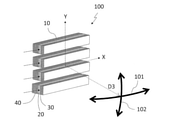
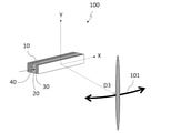
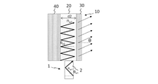
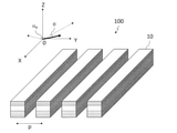
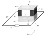
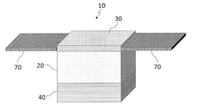
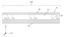
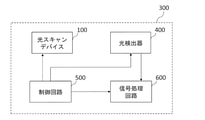
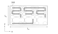
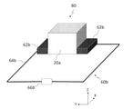
図1は、本開示の例示的な実施形態における光スキャンデバイス100の構成を模式的に示す斜視図である。光スキャンデバイス100は、第1の方向(図1におけるY方向)に規則的に配列された複数の導波路素子10を含む導波路アレイを備える。複数の導波路素子10の各々は、第1の方向に交差する第2の方向(図1におけるX方向)に延びた形状を有する。複数の導波路素子10は、第2の方向に光を伝搬させながら、第1および第2の方向に平行な仮想的な平面に交差する第3の方向D3に光を出射させる。本実施形態では、第1の方向(Y方向)と第2の方向(X方向)とが直交しているが、両者が直交していなくてもよい。本実施形態では、複数の導波路素子10がY方向に等間隔で並んでいるが、必ずしも等間隔に並んでいる必要はない。
FIG. 1 is a perspective view schematically showing a configuration of an
なお、本願の図面に示される構造物の向きは、説明のわかりやすさを考慮して設定されており、本開示の実施形態が現実に実施されるときの向きをなんら制限するものではない。また、図面に示されている構造物の全体または一部分の形状および大きさも、現実の形状および大きさを制限するものではない。 The orientation of the structure shown in the drawings of the present application is set in consideration of easy-to-understand explanation, and does not limit the orientation when the embodiment of the present disclosure is actually implemented. Also, the shape and size of all or part of the structure shown in the drawings does not limit the actual shape and size.
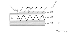
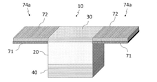
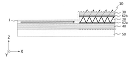
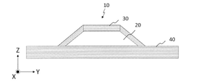
複数の導波路素子10のそれぞれは、互いに対向する第1のミラー30および第2のミラー40(以下、単にミラーと呼ぶ場合がある)と、ミラー30とミラー40の間に位置する光導波層20とを備える。ミラー30および40の各々は、第3の方向D3に交差する反射面を、光導波層20との界面に有する。ミラー30および40、ならびに光導波層20は、第2の方向(X方向)に延びた形状を有している。
Each of the plurality of
なお、後述するように、複数の導波路素子10の複数の第1のミラー30は、一体に構成された第3のミラーの複数の部分であってもよい。また、複数の導波路素子10の複数の第2のミラー40は、一体に構成された第4のミラーの複数の部分であってもよい。さらに、複数の導波路素子10の複数の光導波層20は、一体に構成された光導波層の複数の部分であってもよい。少なくとも、(1)各第1のミラー30が他の第1のミラー30と別体に構成されているか、(2)各第2のミラー40が他の第2のミラー40と別体に構成されているか、(3)各光導波層20が他の光導波層20と別体に構成されていることにより、複数の導波路を形成することができる。「別体に構成されている」とは、物理的に空間を設けることのみならず、間に屈折率が異なる材料を挟み、分離することも含む。
As will be described later, the plurality of
第1のミラー30の反射面と第2のミラー40の反射面とは略平行に対向している。2つのミラー30および40のうち、少なくとも第1のミラー30は、光導波層20を伝搬する光の一部を透過させる特性を有する。言い換えれば、第1のミラー30は、当該光について、第2のミラー40よりも高い光透過率を有する。このため、光導波層20を伝搬する光の一部は、第1のミラー30から外部に出射される。このようなミラー30および40は、例えば誘電体による多層膜(「多層反射膜」と称することもある。)によって形成される多層膜ミラーであり得る。
The reflective surface of the
それぞれの導波路素子10に入力する光の位相を制御し、さらに、これらの導波路素子10における光導波層20の屈折率および厚さの少なくとも一方を同期して(同時に)変化させることで、光による2次元スキャンを実現することができる。
By controlling the phase of the light input to each
本発明者らは、そのような2次元スキャンを実現するために、導波路素子10の動作原理について詳しく分析を行った。その結果に基づき、複数の導波路素子10を同期して駆動することで、光による2次元スキャンを実現することに成功した。
In order to realize such a two-dimensional scan, the present inventors have analyzed in detail the operating principle of the
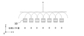
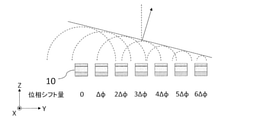
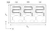
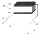
図1に示されるように、各導波路素子10に光を入力すると、各導波路素子10の出射面から光が出射される。出射面は、第1のミラー30の反射面の反対側に位置する。その出射光の方向D3は、光導波層の屈折率、厚さ、および光の波長に依存する。本実施形態では、各導波路素子10から出射される光が概ね同じ方向になるように、各光導波層の屈折率および厚さの少なくとも一方が同期して制御される。これにより、複数の導波路素子10から出射される光の波数ベクトルのX方向の成分を変化させることができる。言い換えれば、出射光の方向D3を、図1に示される方向101に沿って変化させることができる。
As shown in FIG. 1, when light is input to each
さらに、複数の導波路素子10から出射される光は同じ方向を向いているので、出射光は互いに干渉する。それぞれの導波路素子10から出射される光の位相を制御することにより、干渉によって光が強め合う方向を変化させることができる。例えば、同じサイズの複数の導波路素子10がY方向に等間隔で並んでいる場合、複数の導波路素子10には、一定量ずつ位相の異なる光が入力される。その位相差を変化させることにより、出射光の波数ベクトルの、Y方向の成分を変化させることができる。言い換えれば、複数の導波路素子10に導入される光の位相差をそれぞれ変化させることにより、干渉によって出射光が強め合う方向D3を、図1に示される方向102に沿って変化させることができる。これにより、光による2次元スキャンを実現することができる。
Further, since the light emitted from the plurality of
以下、光スキャンデバイス100の動作原理をより詳細に説明する。
Hereinafter, the operating principle of the
<導波路素子の動作原理>
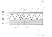
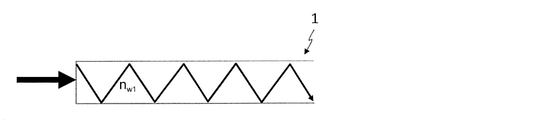
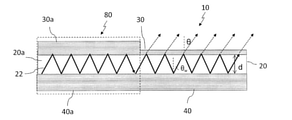
図2は、1つの導波路素子10の断面の構造および伝搬する光の例を模式的に示す図である。図2では、図1に示すX方向およびY方向に垂直な方向をZ方向とし、導波路素子10のXZ面に平行な断面が模式的に示されている。導波路素子10において、一対のミラー30とミラー40が光導波層20を挟むように配置されている。光導波層20のX方向における一端から導入された光22は、光導波層20の上面(図2における上側の表面)に設けられた第1のミラー30および下面(図2における下側の表面)に設けられた第2のミラー40によって反射を繰り返しながら光導波層20内を伝搬する。第1のミラー30の光透過率は第2のミラー40の光透過率よりも高い。このため、主に第1のミラー30から光の一部を出力することができる。
<Operating principle of waveguide element>
FIG. 2 is a diagram schematically showing an example of a cross-sectional structure of one
通常の光ファイバーなどの導波路では、全反射を繰り返しながら光が導波路に沿って伝搬する。これに対して、本実施形態における導波路素子10では、光は光導波層20の上下に配置されたミラー30および40によって反射を繰り返しながら伝搬する。このため、光の伝搬角度(ミラー30または40と光導波層20との界面への入射角度)に制約がなく、ミラー30または40に対して、より垂直に近い角度で入射する光も伝搬できる。すなわち、全反射の臨界角よりも小さい角度(すなわち、より垂直に近い角度)で界面に入射する光も伝搬できる。このため、光の伝搬方向における光の進行速度(群速度)は自由空間における光速に比べて大きく低下する。これにより、導波路素子10は、光の波長、光導波層20の厚さ、および光導波層20の屈折率の変化に対して光の伝搬条件が大きく変化するという性質を持つ。
In a waveguide such as an ordinary optical fiber, light propagates along the waveguide while repeating total internal reflection. On the other hand, in the
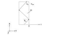
導波路素子10の光の伝搬について、より詳しく説明する。光導波層20の屈折率をnw、光導波層20の厚さをdとする。ここで、光導波層20の厚さdは、ミラー30または40の反射面の法線方向における光導波層20のサイズである。光の干渉条件を考慮すると、波長λの光の伝搬角度θwは、以下の式(1)を満たす。
![]()
![]()
mはモード次数である。式(1)は、光導波層20内の光が厚さ方向に定在波を形成する条件に相当する。光導波層20内の波長λgがλ/nwのとき、光導波層20の厚さ方向における波長λg’はλ/(nwcosθw)であると考えることができる。光導波層20の厚さdが、光導波層20の厚さ方向における波長λg’の半分λ/(2nwcosθw)の整数倍と等しいとき、定在波が形成される。この条件から式(1)が得られる。なお、式(1)におけるmは定在波の腹(anti-node)の数を表す。
m is the mode order. Equation (1) corresponds to the condition that the light in the
ミラー30および40が多層膜ミラーである場合、反射時にミラー内部にも光が侵入する。このため、厳密には、光が侵入した分の光路長に対応する項を式(1)の左辺に付け加える必要がある。しかし、ミラー内部への光の侵入の影響よりも光導波層20の屈折率nwおよび厚さdの影響の方が遥かに大きいため、式(1)によって基本的な動作を説明できる。
When the
光導波層20内を伝搬する光が、第1のミラー30を通じて外部(典型的には空気)に出射されるときの出射角度θは、スネルの法則にしたがって以下の式(2)のように記述できる。
![]()
![]()
式(2)は、光の出射面において、空気側の光の面方向における波長λ/sinθと、導波路素子10側の光の伝搬方向の波長λ/(nwsinθw)とが等しいという条件から得られる。
Equation (2) states that the wavelength λ / sin θ in the plane direction of light on the air side and the wavelength λ / (n w sin θ w ) in the propagation direction of light on the
式(1)および式(2)より、出射角度θは、以下の式(3)のように記述できる。

式(3)からわかるように、光の波長λ、光導波層20の屈折率nw、および光導波層20の厚さdのいずれかを変えることで光の出射方向を変えることができる。
As can be seen from the equation (3), the light emission direction can be changed by changing any one of the wavelength λ of the light, the refractive index n w of the
例えば、nw=2、d=387nm、λ=1550nm、m=1の場合、出射角度は0°である。この状態から、屈折率をnw=2.2に変化させると、出射角度は約66°に変化する。一方、屈折率を変えずに厚さをd=420nmに変化させると、出射角度は約51°に変化する。屈折率も厚さも変化させずに波長をλ=1500nmに変化させると、出射角度は約30°に変化する。このように、光の波長λ、光導波層20の屈折率nw、および光導波層20の厚さdのいずれかを変えることにより、光の出射方向を大きく変えることができる。
For example, when n w = 2, d = 387 nm, λ = 1550 nm, and m = 1, the emission angle is 0 °. From this state, when the refractive index is changed to n w = 2.2, the emission angle changes to about 66 °. On the other hand, when the thickness is changed to d = 420 nm without changing the refractive index, the emission angle changes to about 51 °. When the wavelength is changed to λ = 1500 nm without changing the refractive index and the thickness, the emission angle changes to about 30 °. In this way, by changing any one of the wavelength λ of the light, the refractive index n w of the
この原理を利用して、光導波層20内を伝搬する光の波長を変化させる波長可変手段を設けることによって光の出射方向を制御することが考えられる。しかしながら、波長可変手段をレーザーなどの光源に組み込むと、光源の構成が複雑になる。
Using this principle, it is conceivable to control the emission direction of light by providing a wavelength tunable means for changing the wavelength of light propagating in the
そこで、本実施形態における光スキャンデバイス100は、光導波層20の屈折率nwおよび厚さdの一方または両方を制御することで、光の出射方向を制御する。本実施形態では、光の波長λは、動作中に変化せず、一定に維持される。波長λは、特に限定されない。例えば、波長λは、一般的なシリコン(Si)により光を吸収することで光を検出するフォトディテクタまたはイメージセンサで高い検出感度が得られる400nm~1100nm(可視光から近赤外光)の波長域に含まれ得る。他の例では、波長λは、光ファイバーまたはSi導波路において伝送損失の比較的小さい1260nm~1625nmの近赤外光の波長域に含まれ得る。なお、これらの波長範囲は一例である。使用される光の波長域は、可視光または赤外光の波長域に限定されず、例えば紫外光の波長域であってもよい。本実施形態では波長の制御は行われないが、屈折率および/または厚さの制御に加えて、波長を変化させる制御を行ってもよい。
Therefore, the
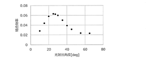
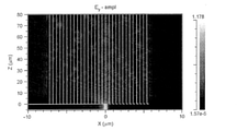
本発明者らは、上記のような特定方向への光の出射が実際に可能であるかを光学解析によって検証した。光学解析は、サイバネット社のDiffractMODを用いた計算によって行った。これは、厳密結合波理論(RCWA:Rigorous Coupled-Wave Analysis)に基づいたシミュレーションであり、波動光学の効果を正確に計算することができる。 The present inventors have verified by optical analysis whether it is actually possible to emit light in a specific direction as described above. Optical analysis was performed by calculation using Cybernet's ResolutionMOD. This is a simulation based on the exact coupled wave theory (RCWA: Rigorous Coupled-Wave Analysis), and the effect of wave optics can be calculated accurately.
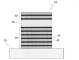
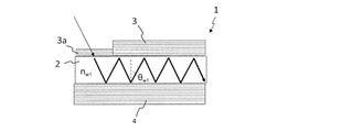
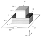
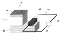
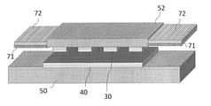
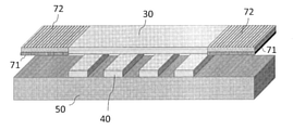
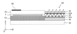
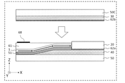
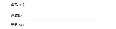
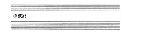
図3は、本シミュレーションにおいて用いた計算モデルを模式的に示す図である。この計算モデルでは、基板50上に、第2のミラー40と、光導波層20と、第1のミラー30とが、この順に積層されている。第1のミラー30および第2のミラー40は、いずれも誘電体多層膜を含む多層膜ミラーである。第2のミラー40は、相対的に屈折率の低い低屈折率層42および相対的に屈折率の高い高屈折率層44を交互に6層ずつ(計12層)積層した構造を有する。第1のミラー30は、低屈折率層42および高屈折率層44を交互に2層ずつ(計4層)積層した構造を有する。ミラー30とミラー40の間に光導波層20が配置されている。導波路素子10および基板50以外の媒質は空気である。
FIG. 3 is a diagram schematically showing the calculation model used in this simulation. In this calculation model, the
このモデルを用いて、光の入射角度を変化させながら入射光に対する光学応答を調べた。これは、空気からの入射光と光導波層20とが、どの程度結合するかを調べることに対応している。入射光が光導波層20と結合する条件では、光導波層20を伝搬した光が外部に出射されるという逆の過程も起きる。よって、入射光が光導波層20と結合する場合の入射角度を求めることは、光導波層20を伝搬した光が外部に出射する際の出射角度を求めることに相当する。入射光が光導波層20と結合すると、光導波層20内において光の吸収および散乱によるロスが生じる。つまり、大きなロスが生じる条件では、入射光が光導波層20に強く結合しているということになる。吸収などによる光のロスがなければ、光の透過率および反射率の合計が1になるが、ロスがあれば、透過率および反射率の合計は1よりも小さくなる。本計算では、光の吸収の影響を取り入れるために、光導波層20の屈折率に虚部を導入し、1から透過率および反射率の合計を引いた値をロスの大きさとして計算した。
Using this model, the optical response to the incident light was investigated while changing the incident angle of the light. This corresponds to investigating how much the incident light from the air and the
本シミュレーションでは、基板50はSi、低屈折率層42はSiO2(厚さ267nm)、高屈折率層44はSi(厚さ108nm)であるものとした。波長λ=1.55μmの光を、角度を様々に変えて入射したときのロスの大きさを計算した。
In this simulation, it is assumed that the
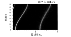
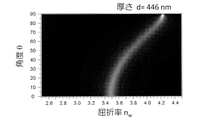
図4Aは、光導波層20の厚さdが704nmの場合における光導波層20の屈折率nwと、モード次数m=1の光の出射角度θとの関係を計算した結果を示している。白い線はロスが大きいことを表している。図4Aに示されているように、nw=2.2付近でモード次数m=1の光の出射角度がθ=0°となる。nw=2.2に近い屈折率をもつ物質には、例えばニオブ酸リチウムがある。
FIG. 4A shows the result of calculating the relationship between the refractive index n w of the
図4Bは、光導波層20の厚さdが446nmの場合における光導波層20の屈折率nwと、モード次数m=1の光の出射角度θとの関係を計算した結果を示している。図4Bに示されているように、nw=3.45付近でモード次数m=1の光の出射角度がθ=0°となる。nw=3.45に近い屈折率をもつ物質には、例えばシリコン(Si)が挙げられる。
FIG. 4B shows the result of calculating the relationship between the refractive index n w of the
このように、光導波層20の厚さdを調整することにより、特定の光導波層20の屈折率nwに対して、特定のモード次数(例えばm=1)の光の出射角度θが0°となるように設計できる。
By adjusting the thickness d of the
図4Aおよび図4Bに示すように、屈折率の変化に応じて、出射角度θが大きく変わることが確認できた。後述するように、屈折率は、例えばキャリア注入、電気光学効果、および熱光学効果などの様々な方法によって変化させることができる。そのような方法による屈折率の変化は0.1程度とあまり大きくない。そのため、これまでは、そのような小さな屈折率の変化では出射角度はそれほど大きく変化しないと考えられていた。しかし、図4Aおよび図4Bに示すように、出射角度がθ=0°となる屈折率付近では、屈折率が0.1増加すると出射角度θが0°から約30°にまで変化することがわかった。このように、本実施形態における導波路素子10では、小さい屈折率変化であっても、出射角度を大きく調整することが可能である。
As shown in FIGS. 4A and 4B, it was confirmed that the emission angle θ changed significantly according to the change in the refractive index. As will be described later, the index of refraction can be varied by various methods such as carrier injection, electro-optic effect, and thermo-optical effect. The change in the refractive index by such a method is not so large as about 0.1. Therefore, until now, it has been considered that the emission angle does not change so much with such a small change in the refractive index. However, as shown in FIGS. 4A and 4B, in the vicinity of the refractive index where the emission angle is θ = 0 °, the emission angle θ may change from 0 ° to about 30 ° when the refractive index increases by 0.1. all right. As described above, in the
同様に、図4Aおよび図4Bの比較からわかるように、光導波層20の厚さdの変化に応じて、出射角度θが大きく変わることが確認できた。後述するように、厚さdは、例えば2つのミラーの少なくとも一方に接続されたアクチュエータによって変化させることができる。厚さdの変化が小さくても、出射角度を大きく調整することができる。
Similarly, as can be seen from the comparison between FIGS. 4A and 4B, it was confirmed that the emission angle θ changes significantly according to the change in the thickness d of the
このように、導波路素子10から出射される光の方向を変えるためには、光導波層20の屈折率nwおよび/または厚さdを変化させればよい。これを実現するために、本実施形態における光スキャンデバイス100は、各導波路素子10における光導波層20の屈折率および厚さの少なくとも一方を変化させる第1調整素子を備える。第1調整素子の構成例については、後述する。
In this way, in order to change the direction of the light emitted from the
以上のように、導波路素子10を用いれば、光導波層20の屈折率nwおよび厚さdの少なくとも一方を変化させることで、光の出射方向を大きく変えることができる。これにより、ミラー30から出射される光の出射角度を、導波路素子10に沿った方向に変化させることができる。このような1次元のスキャンを実現するためには、導波路素子10のアレイを用いる必要はなく、少なくとも1つの導波路素子10を用いればよい。
As described above, if the
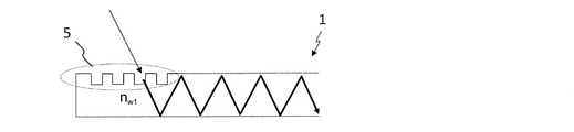
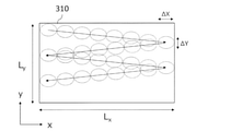
図5は、単一の導波路素子10によって1次元スキャンを実現する光スキャンデバイス100の例を模式的に示す図である。この例では、Y方向に広がりのあるビームスポット(すなわち、光スポット)が形成される。光導波層20の屈折率を変化させることにより、ビームスポットをX方向に沿って移動させることができる。これにより、1次元スキャンが実現される。ビームスポットがY方向に広がりをもつため、一軸方向のスキャンであっても、2次元的に拡がる比較的広いエリアをスキャンすることができる。2次元スキャンが不要な用途では、図5に示すような構成も採用し得る。
FIG. 5 is a diagram schematically showing an example of an
2次元スキャンを実現する場合には、図1に示すように、複数の導波路素子10が配列された導波路アレイが用いられる。複数の導波路素子10内を伝搬する光の位相が特定の条件を満たすとき、光は特定の方向に出射する。その位相の条件が変化すると、光の出射方向が導波路アレイの配列方向にも変化する。すなわち、導波路アレイを用いることにより、2次元スキャンを実現することができる。2次元スキャンを実現するためのより具体的な構成の例については後述する。
When realizing a two-dimensional scan, as shown in FIG. 1, a waveguide array in which a plurality of
以上のように、少なくとも1つの導波路素子10を用いて、導波路素子10における光導波層20の屈折率および厚さの少なくとも一方を変化させることにより、光の出射方向を変化させることができる。しかし、導波路素子10に光を効率的に導入する構成については、改善の余地があった。本開示の実施形態における導波路素子10は、光の全反射を利用する一般的な導波路(以下、「全反射導波路」と称することがある。)とは異なり、光導波層が一対のミラー(例えば多層反射膜)に挟まれた導波路構造(以下、「反射型導波路」と称することがある。)を備える。このような反射型導波路への光の結合については、これまでに十分に検討されてこなかった。本発明者らは、光導波層20に光を効率的に導入するための新規な構造に想到した。
As described above, the light emission direction can be changed by changing at least one of the refractive index and the thickness of the
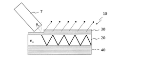
図6Aは、空気およびミラー30を介して間接的に光が光導波層20に入力される構成の例(比較例)を模式的に示す断面図である。本比較例では、反射型導波路である導波路素子10の光導波層20対して、外部から空気およびミラー30を介して間接的に伝播光が導入される。光導波層20に光を導入するためには、光導波層20の内部における導波光の反射角θwに対して、スネルの法則(ninsinθin=nwsinθw)を満たす必要がある。ここで、ninは外部媒質の屈折率、θinは伝播光の入射角、nwは光導波層20の屈折率である。この条件を考慮して入射角θinを調整することにより、光の結合効率を最大化することができる。さらに、この例では、第1のミラー30の一部に多層反射膜の膜数を減らした部分が設けられている。その部分から光が入力されることで結合効率を高めることができる。しかし、このような構成では、光導波層20の伝搬定数の変化(θwavの変化)に応じて、光導波層20への光の入射角θinを変化させる必要が生じる。
FIG. 6A is a cross-sectional view schematically showing an example (comparative example) of a configuration in which light is indirectly input to the
光導波層20の伝搬定数の変化が生じても、光が常に導波路に結合できる状態を保つために、多層反射膜の膜数を減らした部分へ角度広がりのあるビームを入射する方法がある。そのような方法の一例として、図6Bに示すように、導波路素子10に、ミラー30の法線方向に対して角度θinだけ傾けて配置された光ファイバー7によって、外部から空気およびミラー30を介して間接的に光を入射した場合の結合効率について検討する。簡単のため光を光線として考える。通常のシングルモードファイバーの開口数(NA)は0.14程度である。これは角度に換算すると約±8度である。導波路に結合する光の入射角度の範囲は、導波路から出射される光の広がり角と同程度である。出射光の広がり角θdivは、以下の式(4)で表される。

ここでLは伝搬長、λは光の波長、θoutは光の出射角である。Lを10μm以上とすると、θdivは大きくても1度以下である。したがって、光ファイバー7からの光の結合効率は、1/16×100~6.3%以下である。さらに、光の入射角θinを固定し、導波路の屈折率nwを変化させることによって光の出射角θoutを変化させたときの結合効率の変化を計算した結果を図7に示す。結合効率は、入射光のエネルギーに対する導波光のエネルギーの比を表す。図7に示す結果は、入射角θinを30°、導波路膜厚を1.125μm、波長を1.55μmとして、結合効率を計算することによって得られた。この計算では、屈折率nwを1.44~1.78の範囲で変化させることにより、出射角θoutを10°~65°の範囲で変化させた。図7に示すように、このような構成では、結合効率は最大でも7%に満たない。また、出射角θoutを、結合効率がピークになる出射角から20°以上変化させると、結合効率はさらに半分以下に低下する。
Here, L is the propagation length, λ is the wavelength of light, and θ out is the emission angle of light. When L is 10 μm or more, θ div is at most 1 degree or less. Therefore, the coupling efficiency of light from the
このように、光スキャンのために導波路の屈折率等を変化させることによって伝搬定数を変化させると、結合効率はさらに低下する。結合効率を維持するためには、伝搬定数の変化に応じて光の入射角θinを変化させる必要がある。しかし、光の入射角θinを変化させる機構を導入することは、装置構成の複雑化を招き、好ましくない。本発明者らは、屈折率または厚さを変化させる導波路を有する領域の前段に、屈折率および厚さが一定に維持される導波路を有する領域を設けることにより、光入射角を固定する事ができることを見出した。 As described above, if the propagation constant is changed by changing the refractive index or the like of the waveguide for optical scanning, the coupling efficiency is further lowered. In order to maintain the coupling efficiency, it is necessary to change the incident angle θ in of light according to the change of the propagation constant. However, it is not preferable to introduce a mechanism for changing the incident angle θ in of light because the device configuration becomes complicated. The present inventors fix the light incident angle by providing a region having a waveguide in which the refractive index and the thickness are kept constant in front of the region having a waveguide in which the refractive index or the thickness is changed. I found that I could do things.
また、異なる2つの導波路における導波光の結合を考える際に重要な要因が2点ある。1つ目は、伝搬光の伝搬定数であり、2つ目はモードの電界強度分布である。これらが2つの導波路において近いほど結合効率は高くなる。導波路における伝搬光の伝搬定数βは、簡単のため幾何光学的に考えると、β=k・sinθw=(2πnwsinθw)/λで表される。波数をk、導波角度をθw、導波層屈折率をnwとする。全反射型の導波路では、全反射を用いて導波光を導波層に閉じ込めているため、全反射条件であるnwsinθw>1を満たす。一方、スローライト導波路では、導波路の上下に存在する多層反射膜により光を導波路に閉じ込め、導波光の一部を多層反射膜越しに射出するため、nwsinθw<1となる。全反射型導波路と、導波光の一部を射出するスローライト導波路では、伝搬定数は等しくなり得ない。電界強度分布について、図78に示すような全反射導波路の電界強度分布は、図79のような、ピークを導波路内に持ち、導波路外では単調減少する。しかし、図80に示すようなスローライト導波路においては、電界強度分布は図81に示すようになる。導波路内にピークを持つ事は変わらないが、導波光が誘電多層膜内において光の干渉により反射するため、図81に示すように電界強度は誘電多層膜に深く染み出し、また振動的に変化する。以上のように、全反射型導波路とスローライト導波路では、導波光の伝搬定数、電界強度分布共に大きく異なる。よって、全反射型導波路とスローライト導波路を直接的に繋げることは考えられていなかった。本発明者らは、可変の屈折率および/または可変の厚さを有する光導波層に、直接的に全反射導波路を繋げることができることを発見した。 In addition, there are two important factors when considering the coupling of waveguide light in two different waveguides. The first is the propagation constant of the propagating light, and the second is the electric field intensity distribution of the mode. The closer these are in the two waveguides, the higher the coupling efficiency. The propagation constant β of the propagated light in the waveguide is expressed by β = k · sinθ w = (2πn w sinθ w ) / λ in terms of geometrical optics for the sake of simplicity. Let k be the wave number, θ w be the waveguide angle, and n w be the refractive index of the waveguide layer. In the total reflection type waveguide, since the waveguide light is confined in the waveguide layer by using total reflection, the total reflection condition n w sin θ w > 1 is satisfied. On the other hand, in the slow light waveguide, light is confined in the waveguide by the multilayer reflective films existing above and below the waveguide, and a part of the waveguide light is emitted through the multilayer reflective film, so that n w sin θ w <1. Propagation constants cannot be equal in a totally reflective waveguide and a slow light waveguide that emits part of the waveguide light. Regarding the electric field strength distribution, the electric field strength distribution of the total internal reflection waveguide as shown in FIG. 78 has a peak in the waveguide and decreases monotonically outside the waveguide as shown in FIG. 79. However, in the slow light waveguide as shown in FIG. 80, the electric field intensity distribution is as shown in FIG. 81. Although it still has a peak in the waveguide, the waveguide light is reflected by the interference of light in the dielectric multilayer film, so that the electric field strength seeps deeply into the dielectric multilayer film and vibrates as shown in FIG. 81. Change. As described above, the propagation constant and the electric field intensity distribution of the waveguide light are significantly different between the total reflection type waveguide and the slow light waveguide. Therefore, it was not considered to directly connect the total reflection type waveguide and the slow light waveguide. The present inventors have discovered that a total internal reflection waveguide can be directly connected to an optical waveguide layer having a variable index of refraction and / or a variable thickness.
さらに、本発明者らは、そのような2種類の導波路を、共通の基板上に配置することにより、光スキャンデバイスの作製を容易にできることを見出した。すなわち、一体に形成された一つの基板上に2種類の導波路を配置してもよい。一般的な導波路は、半導体プロセスを用いて、基板上に作製される。例えば、蒸着またはスパッタリングなどによる成膜と、リソグラフィーまたはエッチングなどによる微細加工とを組み合わせることによって、基板の上に導波路の構造を作製するのが一般的である。基板の材料として、Si、SiO2、GaAs、GaNなどが挙げられる。 Furthermore, the present inventors have found that by arranging such two types of waveguides on a common substrate, it is possible to easily manufacture an optical scanning device. That is, two types of waveguides may be arranged on one substrate integrally formed. A typical waveguide is made on a substrate using a semiconductor process. For example, it is common to form a waveguide structure on a substrate by combining film formation by vapor deposition or sputtering and microfabrication by lithography or etching. Examples of the substrate material include Si, SiO 2 , GaAs, and GaN.
反射型導波路も、同様の半導体プロセスを用いて作製され得る。反射型導波路では、光導波層を挟む一対のミラーのうち、一方のミラーから光を透過させることよって、光を出射させる。ほとんどの場合、ミラーは、低コストで入手可能なガラス基板の上に作製される。ガラス基板の代わりに、Si、SiO2、GaAs、GaNなどの基板を用いてもよい。 Reflective waveguides can also be made using similar semiconductor processes. In the reflection type waveguide, light is emitted by transmitting light from one of the pair of mirrors sandwiching the optical waveguide layer. In most cases, mirrors are made on a glass substrate that is available at low cost. Instead of the glass substrate, a substrate such as Si, SiO 2 , GaAs, or GaN may be used.
反射型導波路に別の導波路を接続することによって、光を反射型導波路に導入することができる。 Light can be introduced into a reflective waveguide by connecting another waveguide to the reflective waveguide.
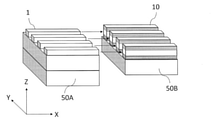
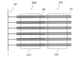
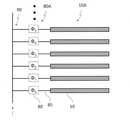
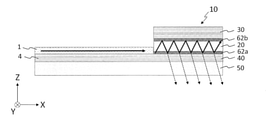
図8は、基板50Aの上に作製された複数の第1の導波路1と、別の基板50Bの上に作製された複数の第2の導波路10との接続を模式的に示す図である。2つの基板50A、50Bは、XY平面に平行に配置されている。複数の第1の導波路1および複数の第2の導波路10は、X方向に延び、Y方向に配列されている。第1の導波路1は、例えば、光の全反射を利用する一般的な導波路である。第2の導波路10は、反射型導波路である。別々の基板50A、50Bの上にそれぞれ配置された第1の導波路1および第2の導波路10を位置合わせして接続することによって、第1の導波路1から第2の導波路10へ光を導入することができる。
FIG. 8 is a diagram schematically showing a connection between a plurality of
第1の導波路1から第2の導波路10へ効率よく光を導入するためには、10nmオーダーの極めて高精度の位置合わせが望まれる。また、高精度の位置合わせができたとしても、2つの基板50A、50Bの熱膨張係数が異なる場合、温度変化により、位置合わせがずれるおそれがある。例えば、Si、SiO2、GaAsおよびGaNの熱膨張係数は、それぞれおよそ4、0.5、6および5(×10―6/K)であり、ガラス基材としてよく使われるBK7の熱膨張係数は、9(×10―6/K)である。別々の基材としてどの材料を組み合わせても、1×10―6/K以上の熱膨張係数の違いが生じる。例えば、複数の第1の導波路1および複数の第2の導波路10の配列方向(図中ではY方向)における2つの基板50A、50Bのサイズが1mmである場合、1°Cの温度変化によって、2つの基板50A、50Bの位置合わせは、1nmずれる。さらに、数十℃の温度変化によって、2つの基板50A、50Bの位置合わせは、数十~百nmのオーダーで大きくずれる。その結果、第1の導波路1から第2の導波路10へ効率よく光を導入することができなくなる。
In order to efficiently introduce light from the
本発明者らは、同じ基板の上に第1の導波路および第2の導波路を配置することにより、上記の課題を解決できることに想到した。共通の基板上にこれらの導波路を配置することにより、第1の導波路および第2の導波路の位置合わせが容易になる。さらに、熱膨張による第1の導波路および第2の導波路の位置合わせのずれが抑制される。その結果、第1の導波路から第2の導波路へ効率よく光を導入することができる。 The present inventors have come up with the idea that the above problems can be solved by arranging the first waveguide and the second waveguide on the same substrate. By arranging these waveguides on a common substrate, the alignment of the first waveguide and the second waveguide becomes easy. Further, the misalignment of the first waveguide and the second waveguide due to thermal expansion is suppressed. As a result, light can be efficiently introduced from the first waveguide to the second waveguide.
本開示のある態様における光スキャンデバイスは、第1の導波路と、前記第1の導波路に繋がる第2の導波路と、前記第1および第2の導波路を支持する基板とを備える。前記第2の導波路は、多層反射膜を有する1のミラーと、前記第1のミラーの前記多層反射膜に対向する多層反射膜を有する第2のミラーと、前記第1のミラーと前記第2のミラーの間に位置し、前記第1の導波路に入力され前記第1の導波路を伝搬した光を伝搬させる光導波層と、を有する。前記第1のミラーは、前記第2のミラーよりも高い光透過率を有し、前記光導波層内を伝搬する光の一部を、前記光導波層の外部に出射する。光スキャンデバイスは、前記光導波層の屈折率および厚さの少なくとも一方を変化させることによって出射光の方向を変化させる調整素子をさらに備える。 The optical scanning device in one aspect of the present disclosure comprises a first waveguide, a second waveguide connected to the first waveguide, and a substrate supporting the first and second waveguides. The second waveguide includes one mirror having a multilayer reflective film, a second mirror having a multilayer reflective film facing the multilayer reflective film of the first mirror, the first mirror, and the first mirror. It is located between the two mirrors and has an optical waveguide layer that is input to the first waveguide and propagates light that has propagated through the first waveguide. The first mirror has a higher light transmittance than the second mirror, and a part of the light propagating in the optical waveguide layer is emitted to the outside of the optical waveguide layer. The optical scanning device further includes an adjusting element that changes the direction of emitted light by changing at least one of the refractive index and the thickness of the optical waveguide layer.
上記態様における「第2の導波路」は、前述の実施形態における「導波路素子」に相当する。本開示の実施形態では、第2の導波路の前段に、屈折率も厚さも一定に維持される第1の導波路が設けられ、第1の導波路に光が入力される。第1の導波路は、入力された光を伝搬させ、第2の導波路の端面から入力する。第1の導波路と第2の導波路とは、端面同士が直接接続されていてもよいし、例えば、端面間にギャップがあってもよい。本明細書において「第1の導波路と第2の導波路とが繋がる」とは、第1の導波路と第2の導波路との間で光の授受が可能な態様で両者が位置していることを意味する。「第1の導波路と第2の導波路とが繋がる」形態は、第1の導波路と第2の導波路とが直接接続されている(すなわち接触している)形態だけでなく、伝搬する光の波長よりも十分に短いギャップを介して両者が配置されている形態も含む。また、本開示で、AがBに「直接的に繋がる」とは、AとBの間で光の授受が可能なように、Aの何れかの部分とBの何れかの部分とがギャップなしに接触することをいう。 The "second waveguide" in the above embodiment corresponds to the "waveguide element" in the above-described embodiment. In the embodiment of the present disclosure, a first waveguide having a constant refractive index and a constant thickness is provided in front of the second waveguide, and light is input to the first waveguide. The first waveguide propagates the input light and inputs it from the end face of the second waveguide. The end faces of the first waveguide and the second waveguide may be directly connected to each other, or for example, there may be a gap between the end faces. In the present specification, "the first waveguide and the second waveguide are connected" means that both are positioned in such a manner that light can be exchanged between the first waveguide and the second waveguide. It means that it is. The form of "connecting the first waveguide and the second waveguide" is not only a form in which the first waveguide and the second waveguide are directly connected (that is, in contact with each other), but also propagation. It also includes a form in which both are arranged via a gap sufficiently shorter than the wavelength of the light to be generated. Further, in the present disclosure, when A is "directly connected" to B, there is a gap between any part of A and any part of B so that light can be exchanged between A and B. It means to contact without.
上記構成によれば、第1の導波路を第2の導波路(導波路素子)の前段に設けることにより、第1の導波路に入射する光の入射角を一定に維持しても、スキャンによる結合効率の低下(すなわちエネルギーのロス)を抑制することができる。 According to the above configuration, by providing the first waveguide in front of the second waveguide (waveguide element), scanning is performed even if the incident angle of the light incident on the first waveguide is kept constant. It is possible to suppress a decrease in coupling efficiency (that is, energy loss) due to the above.
上記構成によれば、同じ基板の上に第1の導波路および第2の導波路を配置することによって、第1の導波路および第2の導波路の位置合わせが容易になる。さらに、熱膨張による第1および第2の導波路の位置合わせのずれが抑制される。その結果、第1の導波路から第2の導波路へ効率よく光を導入することができる。 According to the above configuration, by arranging the first waveguide and the second waveguide on the same substrate, the alignment of the first waveguide and the second waveguide becomes easy. Further, the misalignment of the first and second waveguides due to thermal expansion is suppressed. As a result, light can be efficiently introduced from the first waveguide to the second waveguide.
さらに、第1の導波路の前段に第3の導波路が設けられていてもよい。そのような第3の導波路は、第1の導波路に繋がり、第3の導波路を伝搬した光を、第1の導波路に入力する。ある実施形態において、第3の導波路は全反射導波路であり、第2の導波路は反射型導波路であり得る。第1および第2の導波路を支持する基板は、第3の導波路をさらに支持していてもよい。 Further, a third waveguide may be provided in front of the first waveguide. Such a third waveguide is connected to the first waveguide, and the light propagating through the third waveguide is input to the first waveguide. In certain embodiments, the third waveguide may be a total reflection waveguide and the second waveguide may be a reflection type waveguide. The substrate supporting the first and second waveguides may further support the third waveguide.
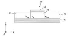
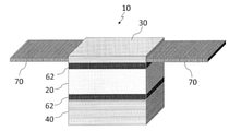
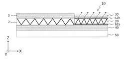
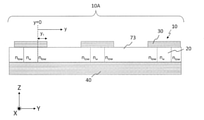
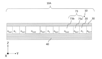
図9は、第1のミラー30と第2のミラー40の間に位置する光導波層20の両隣に、スペーサ73が配置されている構成例を模式的に示す、YZ平面における導波路素子10の断面図である。スペーサ73の屈折率nlowは、光導波層の屈折率nwよりも低い(nlow<nw)。スペーサ73は、例えば、空気でもよい。スペーサ73は、光導波層よりも低い屈折率を有する限り、例えば、TiO2、Ta2O5、SiN、AlN、SiO2などであってもよい。
FIG. 9 schematically shows a configuration example in which spacers 73 are arranged on both sides of the
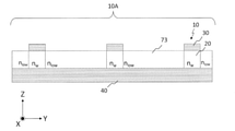
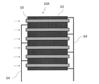
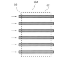
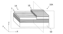
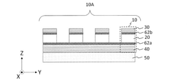
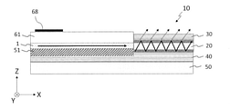
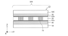
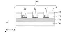
図10は、図9における導波路素子10をY方向に配列した導波路アレイ10Aの構成例を模式的に示す、YZ平面における光スキャンデバイスの断面図である。図10の構成例では、Y方向において、第1のミラー30の幅は、光導波層20の幅と同じである。そのため、第1のミラー30が存在しない領域から導波光が漏れるという課題がある。従来では、複数の反射型導波路も含め、複数の導波路素子10をアレイ化する際に、第1および第2のミラー30および40の少なくとも一方の幅を光導波層20の幅よりも長くすることにより、導波光の漏れを防ぐという発想はなかった。
FIG. 10 is a cross-sectional view of an optical scan device in a YZ plane schematically showing a configuration example of a
光スキャンの性能を向上させるためには、導波路アレイ10Aにおける各導波路素子10を、細線化することが望ましい。この場合、導波光が漏れるという課題はより顕著になる。
In order to improve the performance of optical scanning, it is desirable to make each
導波光が漏れる理由を説明する。 The reason why the waveguide light leaks will be explained.
図11は、光導波層20内において、導波光がX方向に伝搬することを模式的に示す図である。nw>nlowであることから、導波光は、±Y方向において全反射により閉じ込められながら、X方向に伝搬する。しかし、実際には、光導波層20のY方向における端面から外側へ染み出す、エバネッセント光が存在する。また、図2に示すように、導波光は、±Z方向において第1および第2のミラー30および40により反射されながら、全反射角θinよりも小さい角度で、X方向に伝搬する。このとき、図10に示す第1のミラー30が存在しない領域では、エバネッセント光は、反射されず、外に漏れ出る。この意図しない光ロスにより、光スキャンに用いられる光量は低下し得る。
FIG. 11 is a diagram schematically showing that the waveguide light propagates in the X direction in the
本発明者らは、複数の導波路素子10の配列方向において、第1および第2のミラー30および40の少なくとも一方の幅を、光導波層20の幅よりも長くすることにより、上記の課題を解決できることに想到した。これにより、上記の意図しない光ロスを低減することができる。その結果、光スキャンに用いられる光量の低下は抑制される。
The present inventors have made the width of at least one of the first and
また、本発明者らは、以下の光スキャンデバイスにより、光による2次元スキャンを効率よく実現できることに想到した。 In addition, the present inventors have come up with the idea that two-dimensional scanning with light can be efficiently realized by the following optical scanning devices.
本開示の実施形態における光スキャンデバイスは、導波路アレイと、制御回路とを備える。制御回路は、導波路アレイから出射される光の方向を制御して、光で対象領域のスキャンを行う。光導波層に沿った方向におけるスキャン速度と、光導波層に沿った方向に交差する方向におけるスキャン速度とは異なる。制御回路は、対象領域のスキャンを完了するまでに、光導波層に沿った方向、および光導波層に沿った方向に交差する方向のうち、スキャン速度が高い方向に、光スキャンデバイスによって形成される光スポットをより大きく移動させる。これにより、光による2次元スキャンを効率よく実現することができる。 The optical scan device according to the embodiment of the present disclosure includes a waveguide array and a control circuit. The control circuit controls the direction of the light emitted from the waveguide array and scans the target area with the light. The scan speed in the direction along the optical waveguide layer is different from the scan speed in the direction intersecting the direction along the optical waveguide layer. The control circuit is formed by the optical scanning device in the direction along the optical waveguide layer and the direction intersecting the direction along the optical waveguide layer, in which the scanning speed is higher, by the time the scanning of the target area is completed. Moves the light spot more widely. This makes it possible to efficiently realize a two-dimensional scan using light.
本開示は、以下の項目に記載のデバイスを含む。 The present disclosure includes the devices described in the following items.
[項目1]
第1の方向に配列され、各々が前記第1の方向に交差する第2の方向に光を伝搬させる光導波層を備えた複数の導波路素子を含む導波路アレイであって、前記複数の導波路素子から、前記第1および第2の方向に平行な仮想的な平面に交差する第3の方向に光を出射する、導波路アレイと、
各導波路素子における前記光導波層の屈折率および厚さの少なくとも一方を変化させることにより、前記導波路アレイから前記第3の方向に出射される光の波数ベクトルの、前記第2の方向の成分を変化させる第1調整素子と、
前記複数の導波路素子にそれぞれ接続された複数の位相シフタであって、それぞれが、前記複数の導波路素子の対応する1つにおける前記光導波層に直接的にまたは他の導波路を介して繋がる導波路を含む複数の位相シフタと、
前記複数の位相シフタから前記複数の導波路素子へ伝搬する光の位相の差をそれぞれ変化させることにより、前記導波路アレイから前記第3の方向に出射される光の波数ベクトルの、前記第1の方向の成分を変化させる第2調整素子と、
前記第1調整素子および前記第2調整素子を制御して、前記導波路アレイから出射される光によって対象領域のスキャンを行う制御回路と、
を備え、
各導波路素子は、
前記第3の方向に交差する反射面を有し、前記第2の方向に延びる第1のミラーと、
前記第1のミラーの前記反射面に対向する反射面を有し、前記第2の方向に延びる第2のミラーと、
をさらに備え、
前記光導波層は、前記第1のミラーと前記第2のミラーの間に位置し、
前記第1のミラーの前記第1の方向の幅および/または前記第2のミラーの前記第1の方向の幅は、前記光導波層の前記第1の方向の幅よりも幅より長く、
前記第1のミラーは、前記第2のミラーよりも高い光透過率を有し、前記光導波層内を伝搬する光の一部を、前記光導波層の外部に出射し、
前記第1の方向におけるスキャン速度と、前記第2の方向におけるスキャン速度とは異なり、
前記導波路アレイから出射される光によって、前記導波路アレイから離れて配置された前記第1および第2の方向に平行な仮想的な平面に光スポットが形成されるとした場合、前記制御回路は、前記対象領域のスキャンの開始から完了までに、前記第1および第2の方向のうち、前記スキャン速度が低い方向よりも前記スキャン速度が高い方向に前記光スポットを大きく移動させる、
光スキャンデバイス。
[Item 1]
A plurality of waveguide arrays comprising a plurality of waveguide elements arranged in a first direction and each comprising an optical waveguide layer for propagating light in a second direction intersecting the first direction. A waveguide array that emits light from a waveguide element in a third direction intersecting a virtual plane parallel to the first and second directions.
By changing at least one of the refractive index and the thickness of the optical waveguide layer in each waveguide element, the wave vector of the light emitted from the waveguide array in the third direction in the second direction. The first adjusting element that changes the composition and
A plurality of phase shifters, each connected to the plurality of waveguide elements, each directly or via another waveguide in the optical waveguide layer in the corresponding one of the plurality of waveguide elements. Multiple phase shifters, including connected waveguides,
The first wave vector of the light wave vector emitted from the waveguide array in the third direction by changing the phase difference of the light propagating from the plurality of phase shifters to the plurality of waveguide elements. The second adjusting element that changes the component in the direction of
A control circuit that controls the first adjusting element and the second adjusting element to scan the target region by the light emitted from the waveguide array.
Equipped with
Each waveguide element
A first mirror having reflecting surfaces intersecting in the third direction and extending in the second direction.
A second mirror having a reflecting surface facing the reflecting surface of the first mirror and extending in the second direction,
Further prepare
The optical waveguide layer is located between the first mirror and the second mirror.
The width of the first mirror in the first direction and / or the width of the second mirror in the first direction is longer than the width of the optical waveguide layer in the first direction.
The first mirror has a higher light transmittance than the second mirror, and a part of the light propagating in the optical waveguide layer is emitted to the outside of the optical waveguide layer.
The scan speed in the first direction is different from the scan speed in the second direction.
When the light emitted from the waveguide array forms an optical spot on a virtual plane parallel to the first and second directions arranged away from the waveguide array, the control circuit. Moves the light spot significantly in the direction in which the scanning speed is higher than the direction in which the scanning speed is lower among the first and second directions from the start to the completion of scanning the target area.
Optical scanning device.
[項目2]
前記第2の方向における前記スキャン速度は、前記第1の方向における前記スキャン速度よりも高く、
前記制御回路は、前記対象領域のスキャンの開始から完了までに、
前記光スポットを、前記第2の方向および前記第2の方向の逆方向の一方に沿って第1の距離だけ移動させ、
前記光スポットを、前記第1の方向および前記第1の方向の逆方向の一方に沿って、前記第1の距離よりも短い第2の距離だけ移動させ、
前記光スポットを、前記第2の方向および前記第2の方向の逆方向の他方に沿って前記第1の距離だけ移動させ、
前記光スポットを、前記第1の方向および前記第1の方向の逆方向の前記一方に沿って前記第2の距離だけ移動させる動作を2回以上繰り返す、
項目1に記載の光スキャンデバイス。
[Item 2]
The scan speed in the second direction is higher than the scan speed in the first direction.
The control circuit is used from the start to the end of scanning the target area.
The light spot is moved by a first distance along one of the second direction and the opposite direction of the second direction.
The light spot is moved along one of the first direction and the opposite direction of the first direction by a second distance shorter than the first distance.
The light spot is moved by the first distance along the other of the second direction and the opposite direction of the second direction.
The operation of moving the light spot by the second distance along the one of the first direction and the opposite direction of the first direction is repeated two or more times.
The optical scanning device according to
[項目3]
前記第1の方向における前記スキャン速度は、前記第2の方向における前記スキャン速度よりも高く、
前記制御回路は、前記対象領域のスキャンの開始から完了までに、
前記光スポットを、前記第1の方向および前記第1の方向の逆方向の一方に沿って第1の距離だけ移動させ、
前記光スポットを、前記第2の方向および前記第2の方向の逆方向の一方に沿って、前記第1の距離よりも短い第2の距離だけ移動させ、
前記光スポットを、前記第1の方向および前記第1の方向の逆方向の他方に沿って前記第1の距離だけ移動させ、
前記光スポットを、前記第2の方向および前記第2の方向の逆方向の前記一方に沿って前記第2の距離だけ移動させる動作を2回以上繰り返す、
項目1に記載の光スキャンデバイス。
[Item 3]
The scan speed in the first direction is higher than the scan speed in the second direction.
The control circuit is used from the start to the end of scanning the target area.
The light spot is moved by a first distance along one of the first direction and the opposite direction of the first direction.
The light spot is moved along one of the second direction and the opposite direction of the second direction by a second distance shorter than the first distance.
The light spot is moved by the first distance along the other of the first direction and the opposite direction of the first direction.
The operation of moving the light spot by the second distance along the one of the second direction and the opposite direction of the second direction is repeated two or more times.
The optical scanning device according to
[項目4]
前記制御回路は、前記光スキャンデバイスから出射される0次および±1次回折光によって前記対象領域のスキャンを行う、項目1から3のいずれかに記載の光スキャンデバイス。
[Item 4]
The optical scanning device according to any one of
[項目5]
前記第2の方向における前記スキャン速度は、前記第1の方向における前記スキャン速度よりも高く、
前記制御回路は、前記対象領域のスキャンの開始から完了までに、
前記光スポットを、前記第2の方向および前記第2の方向の逆方向の一方に沿って第1の距離だけ移動させると同時に、前記光スポットを、前記第1の方向および前記第1の方向の逆方向の一方に沿って、前記第1の距離よりも短い第2の距離だけ移動させ、
前記光スポットを、前記第2の方向および前記第2の方向の逆方向の他方に沿って前記第1の距離だけ移動させると同時に、前記光スポットを、前記第1の方向および前記第1の方向の逆方向の前記一方に沿って前記第2の距離だけ移動させる
動作を2回以上繰り返す、
項目1に記載の光スキャンデバイス。
[Item 5]
The scan speed in the second direction is higher than the scan speed in the first direction.
The control circuit is used from the start to the end of scanning the target area.
The light spot is moved by a first distance along one of the second direction and the opposite direction of the second direction, and at the same time, the light spot is moved in the first direction and the first direction. Move along one of the opposite directions by a second distance shorter than the first distance.
The light spot is moved by the first distance along the other of the second direction and the opposite direction of the second direction, and at the same time, the light spot is moved in the first direction and the first direction. The operation of moving by the second distance along the one in the opposite direction is repeated twice or more.
The optical scanning device according to
[項目6]
前記第1の方向における前記スキャン速度は、前記第2の方向における前記スキャン速度よりも高く、
前記制御回路は、前記対象領域のスキャンの開始から完了までに、
前記光スポットを、前記第1の方向および前記第1の方向の逆方向の一方に沿って第1の距離だけ移動させると同時に、前記光スポットを、前記第2の方向および前記第2の方向の逆方向の一方に沿って、前記第1の距離よりも短い第2の距離だけ移動させ、
前記光スポットを、前記第1の方向および前記第1の方向の逆方向の他方に沿って前記第1の距離だけ移動させると同時に、前記光スポットを、前記第2の方向および前記第2の方向の逆方向の前記一方に沿って前記第2の距離だけ移動させる
動作を2回以上繰り返す、
項目1に記載の光スキャンデバイス。
[Item 6]
The scan speed in the first direction is higher than the scan speed in the second direction.
The control circuit is used from the start to the end of scanning the target area.
The light spot is moved by a first distance along one of the first direction and the opposite direction of the first direction, and at the same time, the light spot is moved in the second direction and the second direction. Move along one of the opposite directions by a second distance shorter than the first distance.
The light spot is moved by the first distance along the other of the first direction and the opposite direction of the first direction, and at the same time, the light spot is moved in the second direction and the second direction. The operation of moving by the second distance along the one in the opposite direction is repeated twice or more.
The optical scanning device according to
[項目7]
前記制御回路は、クロック信号発生器を含み、前記クロック信号発生器により、前記第1および前記第2調整素子の動作のタイミングを制御する、項目1から6のいずれかに記載の光スキャンデバイス。
[Item 7]
The optical scan device according to any one of
[項目8]
各導波路素子における前記光導波層は、電圧が印加された場合に、前記光導波層を伝搬する光に対する屈折率が変化する材料を含み、
前記第1調整素子は、前記光導波層を挟む第1の一対の電極を備え、前記第1の一対の電極に電圧を印加することにより、前記光導波層の屈折率を変化させ、
各位相シフタにおける前記導波路は、電圧が印加された場合に、前記導波路を伝搬する光に対する屈折率が変化する材料を含み、
前記第2調整素子は、前記導波路を挟む第2の一対の電極を備え、前記第2の一対の電極に電圧を印加することにより、前記導波路の屈折率を変化させ、前記導波路から出力される光の位相を変化させる、項目1に記載の光スキャンデバイス。
[Item 8]
The optical waveguide layer in each waveguide contains a material whose refractive index with respect to light propagating through the optical waveguide layer changes when a voltage is applied.
The first adjusting element includes a first pair of electrodes sandwiching the optical waveguide layer, and by applying a voltage to the first pair of electrodes, the refractive index of the optical waveguide layer is changed.
The waveguide in each phase shifter comprises a material whose refractive index with respect to light propagating through the waveguide changes when a voltage is applied.
The second adjusting element includes a second pair of electrodes that sandwich the waveguide, and by applying a voltage to the second pair of electrodes, the refractive index of the waveguide is changed from the waveguide. The optical scanning device according to
[項目9]
各導波路素子における前記光導波層は、電気光学材料を含み、
前記第1調整素子は、前記光導波層を挟む第1の一対の電極を備え、前記第1の一対の電極に電圧を印加することにより、前記光導波層の屈折率を変化させ、
各位相シフタにおける前記導波路は、液晶材料を含み、
前記第2調整素子は、前記導波路を挟む第2の一対の電極を備え、前記第2の一対の電極に電圧を印加することにより、前記液晶材料の屈折率異方性を変化させ、前記導波路の屈折率を変化させて前記導波路から出力される光の位相を変化させる、項目2または5に記載の光スキャンデバイス。
[Item 9]
The optical waveguide layer in each waveguide element contains an electro-optical material.
The first adjusting element includes a first pair of electrodes sandwiching the optical waveguide layer, and by applying a voltage to the first pair of electrodes, the refractive index of the optical waveguide layer is changed.
The waveguide in each phase shifter comprises a liquid crystal material.
The second adjusting element includes a second pair of electrodes that sandwich the waveguide, and by applying a voltage to the second pair of electrodes, the refractive index anisotropy of the liquid crystal material is changed to change the refractive index anisotropy. The optical scanning device according to
[項目10]
各導波路素子における前記光導波層は、液晶材料を含み、
前記第1調整素子は、前記光導波層を挟む第1の一対の電極を備え、前記第1の一対の電極に電圧を印加することにより、前記液晶材料の屈折率異方性を変化させ、前記光導波層の屈折率を変化させ、
各位相シフタにおける前記導波路は、電気光学材料を含み、
前記第2調整素子は、前記導波路を挟む第2の一対の電極を備え、前記第2の一対の電極に電圧を印加することにより、前記導波路の屈折率を変化させて前記導波路から出力される光の位相を変化させる、項目3または6に記載の光スキャンデバイス。
[Item 10]
The optical waveguide layer in each waveguide element contains a liquid crystal material.
The first adjusting element includes a first pair of electrodes sandwiching the optical waveguide layer, and by applying a voltage to the first pair of electrodes, the refractive index anisotropy of the liquid crystal material is changed. By changing the refractive index of the optical waveguide layer,
The waveguide in each phase shifter comprises an electro-optical material.
The second adjusting element includes a second pair of electrodes that sandwich the waveguide, and by applying a voltage to the second pair of electrodes, the refractive index of the waveguide is changed from the waveguide. The optical scanning device according to
[項目11]
各導波路素子における前記光導波層は、半導体材料を含み、
前記第1調整素子は、前記光導波層を挟む第1の一対の電極を備え、
前記第1の一対の電極の一方、または前記第1の一対の電極の一方と前記光導波層との間には、p型半導体が含まれ、
前記第1の一対の電極の他方、または前記第1の一対の電極の他方と前記光導波層との間には、n型半導体が含まれ、
前記第1調整素子は、前記第1の一対の電極に電圧を印加することにより、前記半導体材料にキャリアを注入し、前記光導波層の屈折率を変化させ、
各位相シフタにおける前記導波路は、液晶材料を含み、
前記第2調整素子は、前記光導波層を挟む第2の一対の電極を備え、前記第2の一対の電極に電圧を印加することにより、前記液晶材料の屈折率異方性を変化させ、前記導波路の屈折率を変化させて前記導波路から出力される光の位相を変化させる、項目2または5に記載の光スキャンデバイス。
[Item 11]
The optical waveguide layer in each waveguide element contains a semiconductor material.
The first adjusting element includes a first pair of electrodes sandwiching the optical waveguide layer.
A p-type semiconductor is included between one of the first pair of electrodes or one of the first pair of electrodes and the optical waveguide layer.
An n-type semiconductor is included between the other of the first pair of electrodes or the other of the first pair of electrodes and the optical waveguide layer.
The first adjusting element injects carriers into the semiconductor material by applying a voltage to the first pair of electrodes to change the refractive index of the optical waveguide layer.
The waveguide in each phase shifter comprises a liquid crystal material.
The second adjusting element includes a second pair of electrodes sandwiching the optical waveguide layer, and by applying a voltage to the second pair of electrodes, the refractive index anisotropy of the liquid crystal material is changed. The optical scan device according to
[項目12]
各導波路素子における前記光導波層は、液晶材料を含み、
前記第1調整素子は、前記光導波層を挟む第1の一対の電極を備え、前記第1の一対の電極に電圧を印加することにより、前記液晶材料の屈折率異方性を変化させ、前記導波路の屈折率を変化させ、
各位相シフタにおける前記導波路は、半導体材料を含み、
前記第2調整素子は、前記光導波層を挟む第2の一対の電極を備え、
前記第2の一対の電極の一方、または前記第2の一対の電極の一方と前記導波路との間には、p型半導体が含まれ、
前記第2の一対の電極の他方、または前記第2の一対の電極の他方と前記導波路との間には、n型半導体が含まれ、
前記第2調整素子は、前記第2の一対の電極に電圧を印加することにより、前記半導体材料にキャリアを注入し、前記導波路の屈折率を変化させて前記導波路から出力される光の位相を変化させる、項目3または6に記載の光スキャンデバイス。
[Item 12]
The optical waveguide layer in each waveguide element contains a liquid crystal material.
The first adjusting element includes a first pair of electrodes sandwiching the optical waveguide layer, and by applying a voltage to the first pair of electrodes, the refractive index anisotropy of the liquid crystal material is changed. By changing the refractive index of the waveguide,
The waveguide in each phase shifter comprises a semiconductor material.
The second adjusting element includes a second pair of electrodes sandwiching the optical waveguide layer.
A p-type semiconductor is included between one of the second pair of electrodes or one of the second pair of electrodes and the waveguide.
An n-type semiconductor is included between the other of the second pair of electrodes or the other of the second pair of electrodes and the waveguide.
The second adjusting element injects carriers into the semiconductor material by applying a voltage to the second pair of electrodes, changes the refractive index of the waveguide, and outputs light from the waveguide. The optical scanning device according to
[項目13]
前記第1の方向および前記第2の方向は直交する、項目1から12のいずれかに記載の光スキャンデバイス。
[Item 13]
The optical scanning device according to any one of
[項目14]
前記複数の導波路素子は、前記第1の方向に等間隔に配列されている、項目1から13のいずれかに記載の光スキャンデバイス。
[Item 14]
The optical scanning device according to any one of
[項目15]
前記複数の導波路素子のうちの隣接する2つの導波路素子の前記第1の方向における中心間距離をpとし、
各導波路素子における前記光導波層を伝搬する光の自由空間における中心波長をλとするとき、
λ/2≦p≦λ/sin10o
の関係を満たす、項目1から14のいずれかに記載の光スキャンデバイス。
[Item 15]
Let p be the distance between the centers of two adjacent waveguide elements in the plurality of waveguide elements in the first direction.
When the central wavelength of the light propagating in the optical waveguide layer in each waveguide element in the free space is λ,
λ / 2 ≦ p ≦ λ / sin10 o
The optical scanning device according to any one of
[項目16]
前記第1および第2のミラーの少なくとも一方は、誘電体多層膜を含む、項目1から15のいずれかに記載の光スキャンデバイス。
[Item 16]
The optical scanning device according to any one of
[項目17]
第1の方向に配列され、各々が前記第1の方向に交差する第2の方向に光を伝搬させる光導波層を備えた複数の導波路素子を含む導波路アレイであって、前記複数の導波路素子から、前記第1および第2の方向に平行な仮想的な平面に交差する第3の方向に光を出射する、導波路アレイと、
各導波路素子における前記光導波層の屈折率および厚さの少なくとも一方を変化させることにより、前記導波路アレイから前記第3の方向に出射される光の波数ベクトルの、前記第2の方向の成分を変化させる第1調整素子と、
前記複数の導波路素子にそれぞれ接続された複数の位相シフタであって、それぞれが、前記複数の導波路素子の対応する1つにおける前記光導波層に直接的にまたは他の導波路を介して繋がる導波路を含む複数の位相シフタと、
前記複数の位相シフタから前記複数の導波路素子へ伝搬する光の位相の差をそれぞれ変化させることにより、前記導波路アレイから前記第3の方向に出射される光の波数ベクトルの、前記第1の方向の成分を変化させる第2調整素子と、
前記第1調整素子および前記第2調整素子を制御して、前記導波路アレイから出射される光によって対象領域のスキャンを行う制御回路と、
を備え、
各導波路素子は、
前記第3の方向に交差する反射面を有し、前記第2の方向に延びる第1のミラーと、
前記第1のミラーの前記反射面に対向する反射面を有し、前記第2の方向に延びる第2のミラーと、
をさらに備え、
前記光導波層は、前記第1のミラーと前記第2のミラーの間に位置し、可変の厚さおよび/または前記光に対する可変の屈折率を有し、
前記第1のミラーの前記第1の方向の幅および/または前記第2のミラーの前記第1の方向の幅は、前記光導波層の前記第1の方向の幅よりも幅より長く、
前記第1のミラーは、前記第2のミラーよりも高い光透過率を有し、前記光導波層内を伝搬する光の一部を、前記光導波層の外部に出射し、
前記第1の方向におけるスキャン速度と、前記第2の方向におけるスキャン速度とは異なり、
前記導波路アレイから出射される光によって、前記導波路アレイから離れて配置された前記第1および第2の方向に平行な仮想的な平面に光スポットが形成されるとした場合、前記制御回路は、前記対象領域のスキャンの開始から完了までに、前記第1および第2の方向のうち、前記スキャン速度が低い方向よりも前記スキャン速度が高い方向に前記光スポットを大きく移動させる、
光スキャンデバイス。
[Item 17]
A plurality of waveguide arrays comprising a plurality of waveguide elements arranged in a first direction and each comprising an optical waveguide layer for propagating light in a second direction intersecting the first direction. A waveguide array that emits light from a waveguide element in a third direction intersecting a virtual plane parallel to the first and second directions.
By changing at least one of the refractive index and the thickness of the optical waveguide layer in each waveguide element, the wave vector of the light emitted from the waveguide array in the third direction in the second direction. The first adjusting element that changes the composition and
A plurality of phase shifters, each connected to the plurality of waveguide elements, each directly or via another waveguide in the optical waveguide layer in the corresponding one of the plurality of waveguide elements. Multiple phase shifters, including connected waveguides,
The first wave vector of the light wave vector emitted from the waveguide array in the third direction by changing the phase difference of the light propagating from the plurality of phase shifters to the plurality of waveguide elements. The second adjusting element that changes the component in the direction of
A control circuit that controls the first adjusting element and the second adjusting element to scan the target region by the light emitted from the waveguide array.
Equipped with
Each waveguide element
A first mirror having reflecting surfaces intersecting in the third direction and extending in the second direction.
A second mirror having a reflecting surface facing the reflecting surface of the first mirror and extending in the second direction,
Further prepare
The optical waveguide is located between the first mirror and the second mirror and has a variable thickness and / or a variable index of refraction for the light.
The width of the first mirror in the first direction and / or the width of the second mirror in the first direction is longer than the width of the optical waveguide layer in the first direction.
The first mirror has a higher light transmittance than the second mirror, and a part of the light propagating in the optical waveguide layer is emitted to the outside of the optical waveguide layer.
The scan speed in the first direction is different from the scan speed in the second direction.
When the light emitted from the waveguide array forms an optical spot on a virtual plane parallel to the first and second directions arranged away from the waveguide array, the control circuit. Moves the light spot significantly in the direction in which the scanning speed is higher than the direction in which the scanning speed is lower among the first and second directions from the start to the completion of scanning the target area.
Optical scanning device.
本開示において、「光」とは、可視光(波長が約400nm~約700nm)だけでなく、紫外線(波長が約10nm~約400nm)および赤外線(波長が約700nm~約1mm)を含む電磁波を意味する。本明細書において、紫外線を「紫外光」と称し、赤外線を「赤外光」と称することがある。 In the present disclosure, "light" refers to electromagnetic waves including not only visible light (wavelength of about 400 nm to about 700 nm) but also ultraviolet rays (wavelength of about 10 nm to about 400 nm) and infrared rays (wavelength of about 700 nm to about 1 mm). means. In the present specification, ultraviolet light may be referred to as "ultraviolet light" and infrared light may be referred to as "infrared light".
本開示において、光による「スキャン」とは、光の方向を変化させることを意味する。「1次元スキャン」とは、光の方向を、当該方向に交差する方向に沿って直線的に変化させることを意味する。「2次元スキャン」とは、光の方向を、当該方向に交差する平面に沿って2次元的に変化させることを意味する。 In the present disclosure, "scanning" by light means changing the direction of light. "One-dimensional scan" means changing the direction of light linearly along a direction that intersects that direction. "Two-dimensional scanning" means changing the direction of light two-dimensionally along a plane that intersects the direction.
以下、本開示の実施形態をより具体的に説明する。ただし、必要以上に詳細な説明は省略する場合がある。例えば、既によく知られた事項の詳細説明および実質的に同一の構成に対する重複する説明を省略することがある。これは、以下の説明が不必要に冗長になることを避け、当業者の理解を容易にするためである。なお、発明者らは、当業者が本開示を十分に理解するために添付図面および以下の説明を提供するのであって、これらによって請求の範囲に記載の主題を限定することを意図するものではない。以下の説明において、同一または類似する構成要素については、同じ参照符号を付している。 Hereinafter, embodiments of the present disclosure will be described in more detail. However, more detailed explanation than necessary may be omitted. For example, detailed explanations of already well-known matters and duplicate explanations for substantially the same configuration may be omitted. This is to avoid unnecessary redundancy of the following description and to facilitate the understanding of those skilled in the art. It should be noted that the inventors provide the accompanying drawings and the following description in order for those skilled in the art to fully understand the present disclosure, and are not intended to limit the subject matter described in the claims by these. do not have. In the following description, the same or similar components are designated by the same reference numerals.
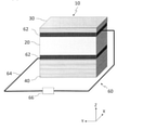
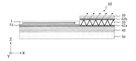
(実施形態)
図12は、本開示の例示的な実施形態における光スキャンデバイスの構造の一部を模式的に示す断面図である。この光スキャンデバイスは、第1の導波路1と、第1の導波路に繋がる第2の導波路(導波路素子)10とを備える。第2の導波路10は、多層反射膜を有する第1のミラー30と、第1のミラー30の多層反射膜に対向する多層反射膜を有する第2のミラー40と、第1のミラー30および第2のミラー40の間に位置する光導波層20とを有する。光導波層20は、第1の導波路1に入力され第1の導波路1を伝搬した光を伝搬させる。光導波層20は、第1の導波路1の導波方向と同じ方向に光を伝搬させる。第1のミラー30は、第2のミラー40よりも高い光透過率を有し、光導波層20内を伝搬する光の一部を、光導波層20の外部に出射する。図12には示されていないが、光スキャンデバイス100は、光導波層20の屈折率および厚さの少なくとも一方を変化させる調整素子をさらに備える。光導波層20は、例えば、電圧が印加された場合に、光導波層20を伝搬する光に対する屈折率が変化する材料を含む。調整素子は、光導波層20に電圧を印加することにより、光導波層20の屈折率を変化させることで、第2の導波路10から出射される光の方向を変化させる。
(Embodiment)
FIG. 12 is a cross-sectional view schematically showing a part of the structure of the optical scanning device according to the exemplary embodiment of the present disclosure. This optical scanning device includes a
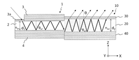
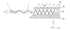
第1の導波路1は、対向する2つの多層反射膜3、4と、2つの多層反射膜3、4に挟まれた光導波層2とを有する。第1の導波路1における多層反射膜3、4は、導波光をロスなく伝えるために、第2の導波路10における光出射側の多層反射膜(第1のミラー30)よりも高い反射率(低い透過率)をもつことが望ましい。よって、多層反射膜3、4の膜厚は、第1のミラー30における膜厚よりも大きいことが望ましい。第1の導波路1の屈折率、すなわち、第1の導波路1における光導波層2の屈折率は、変化しない又は光導波層20の屈折率と異なる量変化する。また、光導波層2の厚さは、変化しない又は光導波層20の厚さと異なる量変化する。第1の導波路1は、第2の導波路10における光導波層20に直接的に繋がっている。例えば、第1の導波路1における光導波層2の端面は、第2の導波路10における光導波層20の端面に接続されている。この例における多層反射膜3は、隣接する部位よりも膜厚が薄い(すなわち反射率が低い)箇所3aを有する。この箇所3a(「光入力部3a」とも称する。)から光が入力される。このように反射率の低い領域から光を入力することにより、効率よく光導波層2に光を導入することができる。光導波層2は、光入力部3aに入射した光を伝搬させ、第2の導波路10における光導波層20の端面に入力する。これにより、光導波層2から光導波層20へ光を伝搬させ、ミラー30から出射することができる。
The
第2の導波路10においては、光を出射する必要があることから、第1のミラー30の多層反射膜の反射率は、第2のミラー40の多層反射膜の反射率よりも低い。第1の導波路1においては、光を出射させないようにするために、多層反射膜3、4の反射率が、第2のミラー40の反射率と同程度の大きさに設計されている。
Since it is necessary to emit light in the
このような構造により、光スキャンデバイスは、後述するように、光を効率よく第2の導波路10から出射することができる。
With such a structure, the optical scanning device can efficiently emit light from the
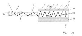
図13は、光スキャンデバイスの構造の他の例を模式的に示す断面図である。この例では、第1の導波路1が、多層反射膜3、4を有していない。第1の導波路1は、全反射によって光を伝搬させる。第1の導波路1は、表面の一部にグレーティング5を有している。グレーティング5を介して光が入力される。この例では、グレーティング5が設けられている箇所が、光入力部として機能する。グレーティング5を設けることにより、光を導波路1内に導入することが容易になる。この例のように多層反射膜3、4がない場合は、導波角度θw1が全反射条件を満たすように設計される。この場合も、第1の導波路1の屈折率は、変化しない又は光導波層20と異なる量変化する。また、第1の導波路1の厚さ、すなわち、光導波層2の厚さは、変化しない又は光導波層20の厚さと異なる量変化する。また、第1の導波路1は、第2の導波路10における光導波層20に直接的に繋がっている。また、光導波層20は、第1の導波路1の導波方向と同じ方向に光を伝搬させる。
FIG. 13 is a cross-sectional view schematically showing another example of the structure of the optical scanning device. In this example, the
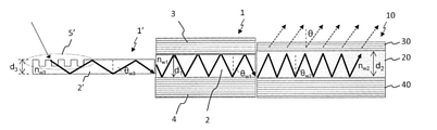
図14は、光スキャンデバイスの構造のさらに他の例を模式的に示す断面図である。この例における光スキャンデバイスは、第1の導波路1に繋がる第3の導波路1’をさらに備えている。第1の導波路1は、反射型導波路であり、対向する2つの多層反射膜3、4と、その間の光導波層2とを有する。一方、第3の導波路1’は、全反射によって光を伝搬させる全反射導波路である。第3の導波路1’の屈折率は、変化しない又は光導波層20と異なる量変化する。また、第3の導波路1’の厚さ、すなわち、光導波層2’の厚さは、変化しない又は光導波層20の厚さと異なる量変化する。また、第3の導波路1’は、第2の導波路10における光導波層20に直接的に繋がっている。また、光導波層20は、第3の導波路1’の導波方向と同じ方向に光を伝搬させる。第3の導波路1’は、図13の例における第1の導波路1と同様、表面の一部にグレーティング5’を有している。グレーティング5’を介して光源からの光が第3の導波路1’内に入力される。この例では、グレーティング5’が設けられている箇所が光入力部として機能する。第2の導波路10における光導波層20は、不図示の調整素子(変調素子)によって屈折率または厚さが変調される。一方、第1の導波路1については、そのような変調機能はない。第1の導波路1からの光の出射を抑えるために、第1の導波路1の反射ミラー(多層反射膜3、4)の反射率は、第2の導波路10の第1のミラー30の反射率よりも高く設定されている。第2の導波路10における第1のミラー30の反射率は、第2のミラー40の反射率よりも低く設定されている。このような構成により、第3の導波路1’に入力された光は、第3の導波路1’および第1の導波路1を伝搬して第2の導波路10に入力される。当該光は、第2の導波路10の光導波層20をさらに伝搬しながら、第1のミラー30を介して外部に出射される。
FIG. 14 is a cross-sectional view schematically showing still another example of the structure of the optical scanning device. The optical scanning device in this example further comprises a third waveguide 1'connected to the
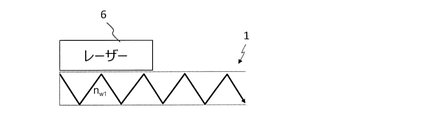
図15および図16Aから図16Cは、第1の導波路1に光が入力される構成において、第1の導波路1への光の入力方法の例を示す図である。図15は、図12に示す例のように、2つの多層反射膜で挟まれた光導波層2への光の入射の一例を示している。図示されるように、多層反射膜の膜厚の薄い箇所(反射率の低い箇所)3aに光を入射することにより、効率よく光を光導波層2に導入することができる。図16Aは、図13に示す例のように、第1の導波路1の表面に設けられたグレーティング5を介して第1の導波路1に光が導入される例を示している。図16Bは、第1の導波路1の端面から光が入力される例を示している。図16Cは、第1の導波路1の表面に設けられたレーザー光源6から、当該表面を介して光が入力される例を示している。図16Cのような構成は、例えば、M. Lamponi et al., “Low-Threshold Heterogeneously Integrated InP/SOI Lasers With a Double Adiabatic Taper Coupler”, IEEE PHOTONICS TECHNOLOGY LETTERS, VOL. 24, NO. 1, JANUARY 1, 2012, pp 76-78.に開示されている。この文献の開示内容全体を本願明細書に援用する。以上の構成によれば、効率よく光を導波路1に入射させることができる。
15 and 16A to 16C are diagrams showing an example of a method of inputting light to the
図15から図16Cに示す光の入力方法は、いずれも、図14に示す第3の導波路1’を用いる構成においても適用できる。図14に示す例では、第3の導波路1’の表面の一部にグレーティング5’が設けられているが、グレーティング5’が設けられていなくてもよい。例えば図16Bまたは図16Cに示す光の入力方法を第3の導波路1’に適用することができる。図16Bに示す光の入力方法を第3の導波路1’に適用する場合、第3の導波路1’は、第3の導波路1’の端面から入射した光を伝搬させ、第1の導波路1の端面に入力する。図16Cに示す光の入力方法を第3の導波路1’に適用する場合、第3の導波路1’の表面に設けられたレーザー光源から、当該表面を介して光が入力される。第3の導波路1’は、入力された光を伝搬させ、第1の導波路1の端面に入力する。また、第3の導波路1’が全反射導波路である必要はなく、図15に示すような反射型導波路であってもよい。
Any of the light input methods shown in FIGS. 15 to 16C can be applied to the configuration using the third waveguide 1'shown in FIG. In the example shown in FIG. 14, the grating 5'is provided on a part of the surface of the third waveguide 1', but the grating 5'may not be provided. For example, the light input method shown in FIG. 16B or FIG. 16C can be applied to the third waveguide 1'. When the light input method shown in FIG. 16B is applied to the third waveguide 1', the third waveguide 1'propagates the light incident from the end face of the third waveguide 1'and causes the first one. Input to the end face of the
図12および図13に示すように、第1の導波路1の光導波層2の屈折率をnw1、第2の導波路10の光導波層20の屈折率をnw2、第2の導波路10からの光の出射角をθ、第1の導波路1における導波光の反射角をθw1、第2の導波路10における導波光の反射角をθw2とする。また、図14に示すように、第3の導波路1’における光導波層2’の屈折率をnw3、第3の導波路1’における導波光の反射角をθw3とする。本実施形態では、第2の導波路10から光を外部(屈折率が1の空気層)に取り出すために、nw2sinθw2=sinθ<1が満足される。
As shown in FIGS. 12 and 13, the refractive index of the
<導波光結合の原理>
以下、図12および図13を参照しながら、導波路1、10間の導波光の結合の原理を説明する。簡単のため、導波路1、10内を伝搬する光を近似的に光線であると考える。導波路10の上下の多層反射膜と光導波層20との界面、および導波路1の上下の多層反射膜と光導波層2との界面(または、光導波層2と外部媒質との界面)で、光が完全に反射されると仮定する。第1の導波路1における光導波層2の厚さをd1、第2の導波路10における光導波層20の厚さをd2とする。導波路1、10のそれぞれにおいて、伝播光が存在する条件は、以下の式(5)、(6)で表される。
2d1nw1cosθw1=mλ (5)
2d2nw2cosθw2=mλ (6)
ここで、λは光の波長、mは1以上の整数である。
<Principle of waveguide optical coupling>
Hereinafter, the principle of coupling of the waveguide light between the
2d 1 n w1 cosθ w1 = mλ (5)
2d 2 n w2 cosθ w2 = mλ (6)
Here, λ is the wavelength of light, and m is an integer of 1 or more.
導波路1、10の界面について、スネルの法則を考慮すると、式(7)が成立する。
nw1sin(90°-θw1)=nw2sin(90°-θw2) (7)
Considering Snell's law for the interfaces of the
n w1 sin (90 ° -θ w1 ) = n w2 sin (90 ° -θ w2 ) (7)
式(7)を変形すると、次の式(8)が得られる。
nw1cosθw1=nw2cosθw2 (8)
By transforming the equation (7), the following equation (8) is obtained.
n w1 cosθ w1 = n w2 cosθ w2 (8)
式(5)および(8)が成立するとき、d1とd2とが等しい場合には、nw2が変化した場合においても式(6)は成立する。つまり、光導波層20の屈折率が変化した場合においても、光導波層2から光導波層20に光が効率よく伝搬するということとなる。
When the equations (5) and (8) are satisfied, if d 1 and d 2 are equal, the equation (6) is established even when n w 2 changes. That is, even when the refractive index of the
上式の導出に際しては簡単のため光を光線として考えたが、実際には厚さd1、d2が波長λと同程度(長くとも波長の10倍以下)であるため、導波光は波動性を有する。したがって、厳密には、上記の屈折率nw1、nw2として、光導波層2、20の材料の屈折率ではなく、有効屈折率を考慮する必要がある。また、光導波層2の厚さd1と光導波層20の厚さd2とが同一ではない場合、または厳密に式(8)を満たしていない場合においても光は光導波層2から光導波層20へ導波され得る。これは、光導波層2から光導波層20への光の伝達が近接場を通じて行われるからである。すなわち、光導波層2の電場分布と光導波層20における電場分布の重なりがあれば、光導波層2から光導波層20へ光が伝達される。
In deriving the above equation, light was considered as a light ray for the sake of simplicity, but in reality, the thicknesses d 1 and d 2 are about the same as the wavelength λ (at the longest, 10 times the wavelength or less), so the waveguide light is a wave. Has sex. Therefore, strictly speaking, it is necessary to consider the effective refractive index as the above-mentioned refractive indexes n w1 and n w2 , not the refractive index of the material of the
以上の議論は、図14に示す例における第3の導波路1’と第1の導波路1との間の導波光についても同様に成立する。
The above discussion is similarly established for the waveguide light between the third waveguide 1'and the
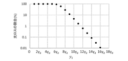
<計算結果>
本実施形態の効果を確認するため、本発明者らは、条件を様々に変えて、光の結合効率を計算した。計算には、Photon Design社のFIMMWAVEを用いた。
<Calculation result>
In order to confirm the effect of the present embodiment, the present inventors calculated the light binding efficiency under various conditions. FIMMWAVE from Photon Design was used for the calculation.
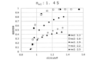
まず、図12に示すように、導波路1、10共に多層反射膜に挟まれている構成について、結合効率を計算した。以下の計算では、導波路1から導波路10に伝搬する光のモードの次数は、m=2であるが、導波路1と導波路10の光のモードの次数が同じであれば、同様の原理により光は結合する。このため、光のモードの次数はm=2に限らない。
First, as shown in FIG. 12, the coupling efficiency was calculated for the configuration in which both the
図17は、nw1を1.45、d1を1.27μm、波長λを1.55μmとした場合の導波路1から導波路10への導波光の結合効率のd2依存性を示している。横軸は、d2を、導波光を光線と仮定した場合のカットオフ膜厚dcutoff(=mλ/(2nw2))で割った値である。縦軸は、ピーク値を1として規格化された結合効率である。計算は、導波光が存在できなくなるカットオフ条件を満たす下限値から、光が外部に射出される上限値まで行った。また、nw2が1.3、1.6、1.9、2.2、2.5のそれぞれの場合について計算を行った。第1の導波路1における厚さ方向の中心と、第2の導波路10における厚さ方向の中心とは同一とした。図17に示す結果から、d2/dcutoffが大きいほど結合効率が高くなることがわかる。d2/dcutoffが小さくなるに従い、モードが存在できなくなり、結合効率は低下する。
FIG. 17 shows the d 2 dependence of the coupling efficiency of the waveguide light from the
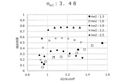
図18は、nw1を3.48、d1を0.5μmに変更して同様の方法で行った計算の結果を示している。この場合も、導波路1から導波路10に伝搬する光のモードの次数は、m=2であるが、前述のとおり光のモードの次数はm=2に限らない。図18からわかるように、d2/dcutoffが大きいほど結合効率が高く、d2/dcutoffが小さくなるに従い、モードが存在できなくなり、結合効率は低下する。
FIG. 18 shows the results of calculations performed in the same manner by changing n w 1 to 3.48 and d 1 to 0.5 μm. Also in this case, the degree of the mode of light propagating from the
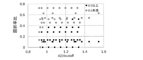
図17および図18において、d2/dcutoffが1よりも低い値においてもモードが存在している(すなわち導波光が結合している)のは、多層反射膜によって反射される際の光の染み出しに起因して、光導波層2の有効厚さがd2よりも厚くなるからである。d2の上限については、光が外部に出射しなくなる値である。この値は、導波光を光線として考え、各導波路の上下の多層反射膜が光を導波路との界面において完全に反射させると仮定すると、導波光の反射角が大気に対し全反射角度になるときのd2である。このとき、次の式(9)が満たされる。
nw2sinθw2=1 (9)
In FIGS. 17 and 18, the mode exists even when the d 2 / d cutoff is lower than 1, (that is, the waveguide light is bonded), that is, the light reflected by the multilayer reflective film is present. This is because the effective thickness of the
n w2 sinθ w2 = 1 (9)
式(6)、式(9)、およびdcutoff=mλ/(2nw2)より、次の式(10)が成立する。
d2/dcutoff=nw2/√(nw2
2-1) (10)
From the equations (6), (9), and dcutoff = mλ / (2n w2 ), the following equation (10) is established.
d 2 / d cutoff = n w2 / √ (n w2 2-1 ) (10)
多層反射膜で反射される際の光の染み出しに起因して、導波光の有効屈折率がnw2よりも低くなる。そのため、式(6)よりもd2の上限値は大きくなる。 The effective refractive index of the waveguide light is lower than n w2 due to the exudation of light when reflected by the multilayer reflective film. Therefore, the upper limit of d 2 is larger than that of the equation (6).
本実施形態の構成において、図6Bに示す構成よりも結合効率が高くなることが好ましい。例えば結合効率が図7に示すピーク値よりも高い7%以上であるという条件を課すと、図17および図18の結果より、
0.95×dcutoff<d2<1.5×dcutoff
(0.95×mλ/(2nw2)<d2<1.5×mλ/(2nw2))
であればよい。
In the configuration of this embodiment, it is preferable that the coupling efficiency is higher than that of the configuration shown in FIG. 6B. For example, if the condition that the binding efficiency is 7% or more, which is higher than the peak value shown in FIG. 7, is imposed, the results of FIGS. 17 and 18 show.
0.95 x d cutoff <d 2 <1.5 x d cutoff
(0.95 × mλ / (2n w2 ) <d 2 <1.5 × mλ / (2n w2 ))
It should be.
図19は、横軸をd2/dcutoff、縦軸を屈折率比(|nw1-nw2|/nw1)とし、結合効率が0.5以上になる場合と、結合効率が0.5未満になる場合とを分類した図である。結合効率が0.5(50%)以上という条件を課す場合、屈折率比が0.4よりも小さく、0.95×dcutoff<d2<1.5×dcutoffであればよい。 In FIG. 19, the horizontal axis is d 2 / d cutoff , the vertical axis is the refractive index ratio (| n w1 -n w2 | / n w1 ), and the bonding efficiency is 0.5 or more and the bonding efficiency is 0. It is a figure which classified the case which becomes less than 5. When the condition that the bonding efficiency is 0.5 (50%) or more is imposed, the refractive index ratio may be smaller than 0.4 and 0.95 × d cutoff <d 2 <1.5 × d cutoff .
本実施形態においては、第1の導波路1の屈折率nw1は、第2の導波路10の屈折率nw2よりも大きい(nw1>nw2)。しかし、本開示はこのような構成に限定されず、nw1≦nw2であってもよい。
In the present embodiment, the refractive index n w1 of the
図20は、第1の導波路1における光導波層2の厚さ方向の中心と、第2の導波路10における光導波層20の厚さ方向の中心とがΔzだけずれた構成を示す図である。Δzの正負は、図20に示すように、第2の導波路10の光導波層20の厚さ方向の中心線が、第1の導波路1の光導波層2の厚さ方向の中心線よりも光放射側(第1のミラー30の側)にあるときを正とする。第1の導波路1の光導波層2の厚さd1と第2の導波路10の光導波層20の厚さd2との差(絶対値)をΔdとする。Δz=Δd/2のとき、導波路1の光導波層2の下部(光放射側とは反対の側)と導波路10の光導波層20の下部のZ方向の位置が一致する。
FIG. 20 is a diagram showing a configuration in which the center in the thickness direction of the
図21は、第1の導波路1から第2の導波路10への光の結合効率のΔz依存性を示す図である。図21の結果は、nw1を2.2、波長λを1.55μm、nw2を2.2、Δdを0.12μmとして、Δzを変えて結合効率を計算することによって得られた。図21に示す結合効率は、Δz=0の場合の値で規格化されている。光導波層2、20の厚さ方向の中心線がZ方向にずれている場合、結合効率はΔzがゼロ(0)の場合よりも低くなる。しかし、-Δd/2<Δz<Δd/2の場合には、Δzが0の場合の結合効率の90%以上になり、比較的高い結合効率を維持できる。
FIG. 21 is a diagram showing the Δz dependence of the light coupling efficiency from the
図13に示す例のように、第1の導波路1が全反射によって光を導波する構成についても、基本的な原理は同じであり、導波路1、10を伝搬する導波光は互いに結合し得る。図13に示す構成についても、第1の導波路1から第2の導波路10への導波光の結合効率のd2依存性を計算によって求めた。図22Aは、nw1を2.2、d1を0.7μm、波長λを1.55μmとした場合における結合効率のd2依存性を示している。図22Bは、nw1を3.48、d1を0.46μm、波長λを1.55μmとした場合における結合効率のd2依存性を示している。前述の例と同様、結合効率が7%以上になるという条件を課す場合、
0.95×dcutoff<d2<1.5×dcutoff
(すなわち、0.95×mλ/(2nw2)<d2<1.5×mλ/(2nw2))
であればよい。
As in the example shown in FIG. 13, the basic principle is the same for the configuration in which the
0.95 × d cutoff <d2 <1.5 × d cutoff
(That is, 0.95 × mλ / (2n w2 ) <d2 <1.5 × mλ / (2n w2 ))
It should be.
また、結合効率が50%以上という条件を課す場合、1.2×dcutoff<d2<1.5×dcutoff(すなわち、1.2×mλ/(2nw2)<d2<1.5×mλ/(2nw2))であればよい。 Further, when the condition that the binding efficiency is 50% or more is imposed, 1.2 × d cutoff <d2 <1.5 × d cutoff (that is, 1.2 × mλ / (2n w2 ) <d2 <1.5 × mλ). / (2n w2 )) may be used.
図13の構成においても、nw1>nw2でもよいし、nw1≦nw2でもよい。 Also in the configuration of FIG. 13, n w1 > n w2 or n w1 ≦ n w2 may be used.
上述した通り、導波路1から導波路10に伝搬する光のモードの次数はm=2に限定されない。例えば、nw1=1.883、d1=0.3μm、nw2=1.6、d2=0.55μmの条件で、図23Aの様なモデルを用いて計算すると、図23Bに示すように、光が導波路に結合することがわかる。
As described above, the order of the modes of light propagating from the
次に、第1の導波路1と第2の導波路10との間にギャップがある場合を検討する。
Next, consider the case where there is a gap between the
図24Aは、本実施形態の変形例を示す断面図である。この例では、第2の導波路10における光導波層20は、ギャップ(例えば空隙)を介して第1の導波路1に繋がっている。このように、第1の導波路1と第2の導波路10との間にギャップが存在する場合であっても、導波モードの近接場を介して光が結合するため、ギャップ幅(X方向の幅)が波長λに比べて十分小さければ、導波光は導波路1、10の間で結合する。これは、図6Aまたは図6Bのように、自由空間における伝播光から導波モードへと結合させる方法とは異なる。
FIG. 24A is a cross-sectional view showing a modified example of the present embodiment. In this example, the
図24Bは、結合効率のギャップ幅依存性の計算結果を示す図である。図24Bにおける結合効率は、ギャップが0μmのときの値を1として規格化された値である。計算では、nw1を3.48、nw2を1.5、d1を0.9μm、d2を1.1μm、ギャップの屈折率を1、波長λを1.55μmとした。図24Bより、規格化された結合効率が50%以上になるのは、ギャップが0.24μm以下の場合である。ギャップが空気以外の媒質である場合、および波長λが1.55μmとは異なる場合を考慮すると、ギャップの光学長(ギャップの屈折率とギャップ幅との積)がλ/6.5以下であれば、規格化された結合効率が50%以上になる。このギャップの光学長は、導波路1、10のパラメータには依存しない。
FIG. 24B is a diagram showing the calculation result of the gap width dependence of the coupling efficiency. The coupling efficiency in FIG. 24B is a value standardized with the value when the gap is 0 μm as 1. In the calculation, n w1 was 3.48, n w2 was 1.5 , d1 was 0.9 μm, d2 was 1.1 μm, the refractive index of the gap was 1 , and the wavelength λ was 1.55 μm. From FIG. 24B, the normalized coupling efficiency is 50% or more when the gap is 0.24 μm or less. Considering the case where the gap is a medium other than air and the case where the wavelength λ is different from 1.55 μm, the optical length of the gap (the product of the refractive index of the gap and the gap width) should be λ / 6.5 or less. For example, the standardized binding efficiency is 50% or more. The optical length of this gap does not depend on the parameters of the
図14に示す例のように、第1の導波路1に、第3の導波路1’から光が入力される形態でも同様に、第3の導波路1’の端面と第1の導波路1の端面との間にギャップがあってもよい。前述のとおり、ギャップの光学長(ギャップの屈折率とギャップ幅との積)は、例えばλ/6.5以下に設定される。
As in the example shown in FIG. 14, even in the form in which light is input to the
次に、本実施形態における第1の導波路1および第2の導波路10の組み合わせ(本明細書において、「導波路ユニット」と称する。)を複数組用いて、2次元的な光のスキャンを実現する構成を説明する。2次元スキャンを実行可能な光スキャンデバイスは、第1の方向に配列された複数の導波路ユニットと、各導波路ユニットを制御する調整素子(例えばアクチュエータおよび制御回路の組み合わせ)を備える。調整素子は、各導波路ユニットにおける第2の導波路10における光導波層20の屈折率および厚さの少なくとも一方を変化させる。これにより、各第2の導波路10から出射される光の方向を変化させることができる。また、複数の導波路ユニットにおける第2の導波路10に、適切に位相差が調整された光が入力されることにより、図1を参照して説明したように、光の2次元スキャンが可能となる。以下、2次元スキャンを実現するための実施形態をより詳細に説明する。
Next, a two-dimensional light scan using a plurality of combinations of the
<2次元スキャンの動作原理>
複数の導波路素子(第2の導波路)10が一方向に配列された導波路アレイにおいて、それぞれの導波路素子10から出射される光の干渉により、光の出射方向は変化する。各導波路素子10に供給する光の位相を調整することにより、光の出射方向を変化させることができる。以下、その原理を説明する。
<Operating principle of 2D scanning>
In a waveguide array in which a plurality of waveguide elements (second waveguides) 10 are arranged in one direction, the light emission direction changes due to the interference of light emitted from each
図25Aは、導波路アレイの出射面に垂直な方向に光を出射する導波路アレイの断面を示す図である。図25Aには、各導波路素子10を伝搬する光の位相シフト量も記載されている。ここで、位相シフト量は、左端の導波路素子10を伝搬する光の位相を基準にした値である。本実施形態における導波路アレイは、等間隔に配列された複数の導波路素子10を含んでいる。図25Aにおいて、破線の円弧は、各導波路素子10から出射される光の波面を示している。直線は、光の干渉によって形成される波面を示している。矢印は、導波路アレイから出射される光の方向(なわち、波数ベクトルの方向)を示している。図25Aの例では、各導波路素子10における光導波層20を伝搬する光の位相はいずれも同じである。この場合、光は導波路素子10の配列方向(Y方向)および光導波層20が延びる方向(X方向)の両方に垂直な方向(Z方向)に出射される。
FIG. 25A is a diagram showing a cross section of a waveguide array that emits light in a direction perpendicular to the emission plane of the waveguide array. FIG. 25A also shows the phase shift amount of the light propagating through each
図25Bは、導波路アレイの出射面に垂直な方向とは異なる方向に光を出射する導波路アレイの断面を示す図である。図25Bの例では、複数の導波路素子10における光導波層20を伝搬する光の位相が、配列方向に一定量(Δφ)ずつ異なっている。この場合、光は、Z方向とは異なる方向に出射される。このΔφを変化させることにより、光の波数ベクトルのY方向の成分を変化させることができる。
FIG. 25B is a diagram showing a cross section of a waveguide array that emits light in a direction different from the direction perpendicular to the emission plane of the waveguide array. In the example of FIG. 25B, the phases of the light propagating in the
導波路アレイから外部(ここでは空気とする。)へ出射される光の方向は、以下のように定量的に議論できる。 The direction of the light emitted from the waveguide array to the outside (here, air) can be quantitatively discussed as follows.
図26は、3次元空間における導波路アレイを模式的に示す斜視図である。互いに直交するX、YおよびZ方向で定義される3次元空間において、光が空気に出射される領域と、導波路アレイとの境界面をZ=z0とする。この境界面は、複数の導波路素子10のそれぞれの出射面を含む。Z<z0では、Y方向に複数の導波路素子10が等間隔に配列され、複数の導波路素子10のそれぞれはX方向に延びている。Z>z0において、空気へ出射される光の電界ベクトルE(x、y、z)は、以下の式(11)で表される。
![]()
![]()
ただしE0は電界の振幅ベクトルであり、kx、kyおよびkzはそれぞれX、YおよびZ方向における波数(wave number)であり、jは虚数単位である。この場合、空気へ出射される光の方向は、図26において太い矢印で表される波数ベクトル(kx、ky、kz)に平行となる。波数ベクトルの大きさは、以下の式(12)で表される。
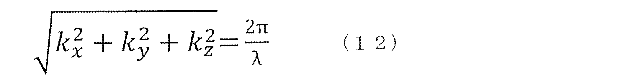
Z=z0における電界の境界条件から、境界面に平行な波数ベクトル成分kxおよびkyは、それぞれ導波路アレイにおける光のX方向およびY方向における波数に一致する。これは、式(2)のスネルの法則と同様に、境界面において、空気側の光が有する面方向の波長と、導波路アレイ側の光が有する面方向の波長とが一致する条件に相当する。 From the boundary condition of the electric field at Z = z 0 , the wave vector components k x and ky parallel to the boundary plane correspond to the wave numbers in the X and Y directions of the light in the waveguide array, respectively. Similar to Snell's law in Eq. (2), this corresponds to the condition that the wavelength in the plane direction of the light on the air side and the wavelength in the plane direction of the light on the waveguide array side match at the boundary surface. do.
kxは、X方向に延びた導波路素子10の光導波層20を伝搬する光の波数に等しい。上述した図2に示される導波路素子10では、kxは、式(2)および式(3)を用いて、以下の式(13)で表される。

kyは、隣接する2つの導波路素子10の間の光の位相差から導出される。Y方向に等間隔に配列されたN本の導波路素子10のそれぞれのY方向の中心をyq(q=0、1、2、・・・、N-1)とし、隣接する2つの導波路素子10の間の距離(中心間距離)をpとする。そのとき、空気へ出射される光の電界ベクトル(式(11))は、境界面内(Z=z0)のyqおよびyq+1において、
![]()

![]()
この場合、yqにおける光の位相はφq=φ0+qΔφとなる(φq+1-φq=Δφ)。つまり、位相φqは、Y方向に沿って、一定(Δφ=0)か、比例して増加(Δφ>0)または減少(Δφ<0)する。Y方向に配列された導波路素子10が等間隔でない場合は、所望のkyに対して、yqおよびyq+1での位相差がΔφq=φq+1-φq=ky(yq+1-yq)となるように設定すればよい。この場合、yqにおける光の位相はφq=φ0+ky(yq-y0)となる。式(14)および式(15)からそれぞれ得られるkxおよびkyを用いれば、式(12)からkzが導出される。これにより、光の出射方向(波数ベクトルの方向)が得られる。
In this case, the phase of light at y q is φ q = φ 0 + q Δφ (φ q + 1 −φ q = Δφ). That is, the phase φ q is constant (Δφ = 0) or proportionally increased (Δφ> 0) or decreased (Δφ <0) along the Y direction. When the
例えば、図26に示すように、出射光の波数ベクトル(kx、ky、kz)と、その波数ベクトルをYZ平面に射影したベクトル(0、ky、kz)とがなす角度をθとする。θは、波数ベクトルとYZ平面とがなす角度である。θは、式(12)および式(13)を用いて、以下の式(16)で表される。
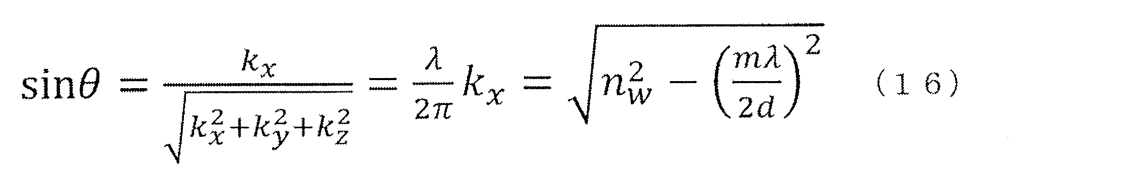
式(16)は、出射光がXZ平面に平行な場合に限定したときの式(3)と全く同じである。式(16)からわかるように、波数ベクトルのX成分は、光の波長、光導波層20の屈折率、および光導波層20の厚さに依存して変化する。
Equation (16) is exactly the same as equation (3) when the emitted light is limited to the case where it is parallel to the XZ plane. As can be seen from equation (16), the X component of the wave vector varies depending on the wavelength of light, the refractive index of the
同様に、図26に示すように、出射光(0次光)の波数ベクトル(kx、ky、kz)と、その波数ベクトルをXZ平面に射影したベクトル(kx、0、kz)とがなす角度をα0とする。α0は、波数ベクトルとXZ平面とがなす角度である。α0は、式(12)および式(13)を用いて、以下の式(17)で表される。

式(17)からわかるように、光の波数ベクトルのY成分は、光の位相差Δφによって変化する。 As can be seen from the equation (17), the Y component of the wave vector of light changes depending on the phase difference Δφ of light.
このように、波数ベクトル(kx、ky、kz)の代わりに、式(16)および式(17)からそれぞれ得られるθおよびα0を用いて光の出射方向を特定することもできる。その場合、光の出射方向を表す単位ベクトルは、(sinθ、sinα0、(1-sin2α0-sin2θ)1/2)と表すことができる。光出射においてこれらのベクトル成分はすべて実数でなければならないので、sin2α0+sin2θ≦1が満たされる。sin2α0≦1-sin2θ=cos2θから、出射光は-cosθ≦sinα0≦cosθを満たす角度範囲で変化することがわかる。-1≦sinα0≦1から、θ=0oでは、出射光は-90o≦α0≦90oの角度範囲で変化する。しかし、θが増加するとcosθは小さくなるので、α0の角度範囲は狭くなる。θ=90o(cosθ=0)では、α0=0oのときのみしか光は出射されない。 In this way, instead of the wave vector (k x , ky, k z ) , θ and α 0 obtained from the equations (16) and (17) can be used to specify the light emission direction. .. In that case, the unit vector representing the light emission direction can be expressed as (sin θ, sin α 0 , (1-sin 2 α 0 − sin 2 θ) 1/2 ). Since all of these vector components must be real numbers in light emission, sin 2 α 0 + sin 2 θ ≦ 1 is satisfied. From sin 2 α 0 ≦ 1-sin 2 θ = cos 2 θ, it can be seen that the emitted light changes in an angle range satisfying −cosθ ≦ sinα 0 ≦ cosθ. From -1 ≤ sin α 0 ≤ 1, when θ = 0 o , the emitted light changes in the angle range of −90 o ≤ α 0 ≤ 90 o . However, as θ increases, cos θ becomes smaller, so the angle range of α 0 becomes narrower. At θ = 90 o (cos θ = 0), light is emitted only when α 0 = 0 o .
本実施形態における光による2次元スキャンは、導波路素子10が少なくとも2本あれば実現できる。しかし、導波路素子10の本数が少ない場合、上記のα0の広がり角度Δαが大きくなる。導波路素子10の本数が増加するとΔαは小さくなる。このことは、以下のようにして説明できる。簡単のために、図26においてθ=0oの場合を考える。つまり、光の出射方向がYZ平面に平行な場合を考える。
The two-dimensional scan with light in the present embodiment can be realized if there are at least two
N本(Nは2以上の整数)の導波路素子10のそれぞれから、同じ出射強度および上述した位相φqを有する光が出射されるとする。そのとき、N本の導波路素子10から出射される合計の光(電界)の振幅分布の絶対値は、遠視野において、以下の式(18)で表されるF(u)に比例する。


αは、YZ平面において、観測点および原点を結ぶ直線と、Z軸とがなす角度である。α0は、式(17)を満たす。式(18)のF(u)は、u=0(α=α0)でN(最大)となり、u=±2π/Nで0となる。u=-2π/Nおよび2π/Nを満たす角度をそれぞれα1およびα2とすると(α1<α0<α2)、α0の広がり角度はΔα=α2-α1となる。-2π/N<u<2π/N(α1<α<α2)の範囲のピークは、一般にメインローブと呼ばれる。メインローブの両側にはサイドローブと呼ばれる複数の小さいピークが存在する。メインローブの幅Δu=4π/Nと、式(19)から得られるΔu=2πpΔ(sinα)/λとを比較すると、Δ(sinα)=2λ/(Np)となる。Δαが小さければ、Δ(sinα)=sinα2-sinα1=[(sinα2-sinα1)/(α2-α1)]Δα~[d(sinα)/dα]α=α0Δα=cosα0Δαとなる。このため、広がり角度は、以下の式(20)で表される。

したがって、導波路素子10の本数が多いほど、広がり角度Δαを小さくすることができ、遠方においても高精細な光スキャンが実現できる。同様の議論は、図26においてθ≠0oの場合にも適用できる。
Therefore, as the number of
<導波路アレイから出射される回折光>
導波路アレイからは0次光のほかに高次の回折光も出射され得る。簡単のために、図26においてθ=0oの場合を考える。つまり、回折光の出射方向はYZ平面に平行である。
<Diffracted light emitted from the waveguide array>
In addition to the 0th-order light, higher-order diffracted light can also be emitted from the waveguide array. For simplicity, consider the case of θ = 0 o in FIG. That is, the emission direction of the diffracted light is parallel to the YZ plane.
図27Aは、pがλよりも大きい場合において、導波路アレイから回折光が出射される様子を示す模式図である。この場合、位相シフトがなければ(α0=0o)、図27Aに示す実線矢印の方向に0次光および±1次光が出射される(pの大きさによっては、さらに高次の回折光も出射され得る)。この状態から位相シフトを与えると(α0≠0o)、図27Aに示す破線矢印のように、0次光および±1次光の出射角度が同じ回転方向に変化する。±1次光のような高次光を用いてビームスキャンを行うことも可能であるが、よりシンプルにデバイスを構成する場合、0次光のみが用いられる。0次光の利得が低減することを回避するために、隣接する2つの導波路素子10の間の距離pをλよりも小さくすることによって高次光の出射を抑制してもよい。p>λであっても、高次光を物理的に遮断することによって0次光のみを用いることも可能である。
FIG. 27A is a schematic diagram showing how diffracted light is emitted from the waveguide array when p is larger than λ. In this case, if there is no phase shift (α 0 = 0 o ), 0th-order light and ± 1st-order light are emitted in the direction of the solid arrow shown in FIG. 27A (depending on the magnitude of p, higher-order diffraction is performed. Light can also be emitted). When a phase shift is applied from this state (α 0 ≠ 0 o ), the emission angles of the 0th-order light and the ± 1st-order light change in the same rotation direction as shown by the broken line arrow shown in FIG. 27A. It is possible to perform beam scanning using higher-order light such as ± 1st-order light, but when the device is configured more simply, only 0th-order light is used. In order to avoid a decrease in the gain of the 0th-order light, the emission of the higher-order light may be suppressed by making the distance p between the two
図27Bは、pがλよりも小さい場合において、導波路アレイから回折光が出射される様子を示す模式図である。この場合、位相シフトがなければ(α0=0o)、高次の回折光は、回折角度が90度を超えるため存在せず、前方には0次光だけが出射する。ただし、pがλに近い値の場合、位相シフトを与えると(α0≠0o)、出射角度の変化に伴って±1次光が出射される場合がある。 FIG. 27B is a schematic diagram showing how diffracted light is emitted from the waveguide array when p is smaller than λ. In this case, if there is no phase shift (α 0 = 0 o ), the higher-order diffracted light does not exist because the diffraction angle exceeds 90 degrees, and only the 0th-order light is emitted forward. However, when p is a value close to λ, when a phase shift is applied (α 0 ≠ 0 o ), ± primary light may be emitted as the emission angle changes.
図27Cは、p~λ/2の場合において、導波路アレイから回折光が出射される様子を示す模式図である。この場合、位相シフトを与えても(α0≠0o)±1次光は出射しない、あるいは出射したとしてもかなり大きな角度で出射する。p<λ/2の場合は、位相シフトを与えても高次の光が出射することはない。しかし、pをこれ以上小さくすることによるメリットも特にない。よって、pは、例えばλ/2以上に設定され得る。 FIG. 27C is a schematic diagram showing how diffracted light is emitted from the waveguide array in the case of p to λ / 2. In this case, even if a phase shift is given (α 0 ≠ 0 o ), ± primary light is not emitted, or even if it is emitted, it is emitted at a considerably large angle. When p <λ / 2, higher-order light is not emitted even if a phase shift is applied. However, there is no particular merit by making p smaller than this. Therefore, p can be set to, for example, λ / 2 or more.
図27Aから図27Cにおける空気へ出射される0次光および±1次光の関係は、以下のように定量的に説明できる。式(18)のF(u)は、F(u)=F(u+2π)であることから、2πの周期関数である。u=±2mπのとき、F(u)=N(最大)となる。そのとき、u=±2mπを満たす出射角度αで±m次光が出射される。u=±2mπ(m≠0)付近のピーク(ピーク幅はΔu=4π/N)をグレーティングローブと呼ぶ。 The relationship between the 0th-order light and the ± 1st-order light emitted from FIG. 27A to the air in FIG. 27C can be quantitatively explained as follows. Since F (u) in the equation (18) is F (u) = F (u + 2π), it is a periodic function of 2π. When u = ± 2mπ, F (u) = N (maximum). At that time, ± mth order light is emitted at an emission angle α satisfying u = ± 2 mπ. A peak near u = ± 2 mπ (m ≠ 0) (peak width is Δu = 4π / N) is called a grating lobe.
高次光のうち、±1次光のみを考えると(u=±2π)、±1次光の出射角度α±は、以下の式(21)を満たす。

+1次光が出射されない条件sinα+>1から、p<λ/(1―sinα0)が得られる。同様に、-1次光が出射されない条件sinα-<-1から、p<λ/(1+sinα0)が得られる。 From the condition sinα + > 1 in which the +1st order light is not emitted, p <λ / (1-sinα 0 ) can be obtained. Similarly, p <λ / (1 + sinα 0 ) can be obtained from the condition sinα − <-1 in which the -1st order light is not emitted.
出射角度α0(>0)の0次光に対して±1次光が出射されるか否かの条件は、以下のように分類される。p≧λ/(1―sinα0)の場合、±1次光の両方が出射される。λ/(1+sinα0)≦p<λ/(1―sinα0)の場合、+1次光は出射されないが-1次光は出射される。p<λ/(1+sinα0)の場合、±1次光はいずれも出射されない。特に、p<λ/(1+sinα0)を満たせば、図26においてθ≠0oの場合でも±1次光は出射されない。例えば、±1次光が出射されない場合において片側10度以上のスキャンを達成するには、α0=10°として、p≦λ/(1+sin10°)~0.85λの関係を満たしていればよい。pに関する前述の下限についての条件と組み合わせれば、λ/2≦p≦λ/(1+sin10°)が満足されていればよい。 The conditions for whether or not ± 1st-order light is emitted with respect to the 0th-order light having an emission angle of α 0 (> 0) are classified as follows. When p ≧ λ / (1-sinα 0 ), both ± primary light are emitted. When λ / (1 + sinα 0 ) ≦ p <λ / (1-sinα 0 ), the +1st order light is not emitted but the -1st order light is emitted. When p <λ / (1 + sinα 0 ), neither ± primary light is emitted. In particular, if p <λ / (1 + sinα 0 ) is satisfied, ± primary light is not emitted even when θ ≠ 0 o in FIG. 26. For example, in order to achieve a scan of 10 degrees or more on one side when ± primary light is not emitted, α 0 = 10 ° and the relationship of p≤λ / (1 + sin10 °) to 0.85λ may be satisfied. .. When combined with the above-mentioned condition for the lower limit of p, it is sufficient that λ / 2 ≦ p ≦ λ / (1 + sin10 °) is satisfied.
しかし、±1次光が出射されない条件を満たすためには、pを非常に小さくする必要がある。これは、導波路アレイの作製を困難にする。そこで、±1次光の有無に関わらず、0次光を0°<α0<αmaxの角度範囲でスキャンすることを考える。ただし、±1次光はこの角度範囲には存在しないとする。この条件を満たすためには、α0=0°において、+1次光の出射角度はα+≧αmaxでなければならず(すなわち、sinα+=(λ/p)≧sinαmax)、α0=αmaxにおいて、-1次光の出射角度はα-≦0でなければならない(すなわち、sinα-=sinαmax-(λ/p)≦0)。これらの制限から、p≦λ/sinαmaxが得られる。 However, in order to satisfy the condition that ± primary light is not emitted, it is necessary to make p very small. This makes it difficult to fabricate a waveguide array. Therefore, consider scanning the 0th-order light in the angle range of 0 ° <α 0 <α max regardless of the presence or absence of ± 1st-order light. However, it is assumed that the ± primary light does not exist in this angle range. In order to satisfy this condition, at α 0 = 0 °, the emission angle of the + 1st order light must be α + ≧ α max (that is, sin α + = (λ / p) ≧ sin α max ), α 0 . At = α max , the emission angle of the -1st order light must be α − ≤ 0 (that is, sin α − = sin α max − (λ / p) ≤ 0). From these limitations, p ≦ λ / sinα max is obtained.
上記の議論から、±1次光がスキャンの角度範囲に存在しない場合における0次光の出射角度α0の最大値αmaxは、以下の式(22)を満たす。

例えば、±1次光がスキャンの角度範囲に存在しない場合において片側10度以上のスキャンを達成するには、αmax=10°として、p≦λ/sin10°~5.76λの関係を満たしていればよい。pに関する前述の下限についての条件と組み合わせれば、λ/2≦p≦λ/sin10°が満足され得る。このpの上限(p~5.76λ)は±1次光が出射されない場合における上限(p~0.85λ)と比べて十分大きいので、導波路アレイの作製は比較的容易である。ここで、使用される光が単一波長の光ではない場合、使用される光の中心波長をλとする。
For example, in order to achieve a scan of 10 degrees or more on one side when ± primary light is not in the angle range of the scan, α max = 10 ° and the relationship of p ≦ λ /
以上のことから、より広い角度範囲をスキャンするためには、導波路間の距離pを小さくする必要がある。一方、pが小さい場合に式(20)における出射光の広がり角度Δαを小さくするためには、導波路アレイの本数を増やす必要がある。導波路アレイの本数は、用途および要求される性能に応じて適宜決定される。導波路アレイの本数は、例えば16本以上、用途によっては100本以上であり得る。 From the above, in order to scan a wider angle range, it is necessary to reduce the distance p between the waveguides. On the other hand, when p is small, it is necessary to increase the number of waveguide arrays in order to reduce the spread angle Δα of the emitted light in the equation (20). The number of waveguide arrays is appropriately determined according to the application and the required performance. The number of waveguide arrays may be, for example, 16 or more, and depending on the application, 100 or more.
<導波路アレイに導入する光の位相制御>
それぞれの導波路素子10から出射される光の位相を制御するためには、導波路素子10に光を導入する前段に、光の位相を変化させる位相シフタを導入すればよい。本実施形態における光スキャンデバイス100は、複数の導波路素子10のそれぞれに接続された複数の位相シフタと、各位相シフタを伝搬する光の位相を調整する第2調整素子とを備える。各位相シフタは、複数の導波路素子10の対応する1つにおける光導波層20に直接的にまたは他の導波路を介して繋がる導波路を含む。第2調整素子は、複数の位相シフタから複数の導波路素子10へ伝搬する光の位相の差をそれぞれ変化させることにより、複数の導波路素子10から出射される光の方向(第3の方向D3)を変化させる。以下の説明では、導波路アレイと同様に、配列された複数の位相シフタを「位相シフタアレイ」と呼ぶことがある。
<Phase control of light introduced into the waveguide array>
In order to control the phase of the light emitted from each
図28は、位相シフタ80が導波路素子10に直接的に接続されている構成の例を示す模式図である。図28において、破線枠で囲まれた部分が位相シフタ80に該当する。この位相シフタ80は、対向する一対のミラー(第5のミラー30aおよび第6のミラー40a、以下、単にミラーと呼ぶことがある。)と、ミラー30aとミラー40aの間に設けられた導波路20aとを有する。この例における導波路20aは、導波路素子10における光導波層20と共通の部材で構成され、光導波層20に直接的に繋がっている。同様に、ミラー40aも、導波路素子10におけるミラー40と共通の部材で構成され、ミラー40に接続されている。ミラー30aは、導波路素子10におけるミラー30よりも低い透過率(高い反射率)を有する。ミラー30aは、ミラー30に接続されている。位相シフタ80では、光を放射しないようにするために、ミラー30aの透過率はミラー40、40aと同様の低い値に設計されている。すなわち、第5のミラー30aと第6のミラー40aの光透過率は、第1のミラー30の光透過率よりも低い。この例では、位相シフタ80が、本開示における「第1の導波路」に相当する。このように、「第1の導波路」は、位相シフタとして機能してもよい。
FIG. 28 is a schematic diagram showing an example of a configuration in which the
図29は、導波路アレイ10Aおよび位相シフタアレイ80Aを、光出射面の法線方向(Z方向)から見た模式図である。図29に示される例では、全ての位相シフタ80が同じ伝搬特性を有し、全ての導波路素子10が同じ伝搬特性を有する。それぞれの位相シフタ80およびそれぞれの導波路素子10は同じ長さであってもよいし、長さが異なっていても良い。それぞれの位相シフタ80の長さが等しい場合は、駆動電圧によりそれぞれの位相シフト量を調整すればよい。また、それぞれの位相シフタ80の長さを等ステップで変化させた構造にすることで、同じ駆動電圧で等ステップの位相シフトを与えることもできる。さらに、この光スキャンデバイス100は、複数の位相シフタ80に光を分岐して供給する光分岐器90と、各導波路素子10を駆動する第1駆動回路110と、各位相シフタ80を駆動する第2駆動回路210とをさらに備えている。図29における直線の矢印は光の入力を示している。別々に設けられた第1駆動回路110と第2駆動回路210とをそれぞれ独立に制御することにより、2次元スキャンを実現できる。この例では、第1駆動回路110は、第1調整素子の1つの要素として機能し、第2駆動回路210は、第2調整素子の1つの要素として機能する。
FIG. 29 is a schematic view of the
第1駆動回路110は、後述するように、各導波路素子10における光導波層20の屈折率または厚さを変化(変調)させることにより、光導波層20から出射する光の角度を変化させる。第2駆動回路210は、後述するように、各位相シフタ80における導波路20aの屈折率を変化させることにより、導波路20aの内部を伝搬する光の位相を変化させる。光分岐器90は、全反射によって光が伝搬する導波路で構成してもよいし、導波路素子10と同様の反射型導波路で構成してもよい。
As will be described later, the
なお、光分岐器90で分岐したそれぞれの光に対して位相を制御した後に、それぞれの光を位相シフタ80に導入してもよい。この位相制御には、例えば、位相シフタ80に至るまでの導波路の長さを調整することによるパッシブな位相制御構造を用いることができる。あるいは、位相シフタ80と同様の機能を有する電気信号で制御可能な位相シフタを用いても良い。このような方法により、例えば、全ての位相シフタ80に等位相の光が供給されるように、位相シフタ80に導入される前に位相を調整してもよい。そのような調整により、第2駆動回路210による各位相シフタ80の制御をシンプルにすることができる。
After controlling the phase of each light branched by the
図30は、位相シフタ80における導波路が、導波路素子10における光導波層20と、他の導波路85を介して繋がる構成の例を模式的に示す図である。他の導波路85は、上述した何れかの第1の導波路1であってもよい。また、他の導波路85は、図14に示した導波路1および1’であってもよい。各位相シフタ80は、図28に示す位相シフタ80と同じ構成を有していてもよいし、異なる構成を有していてもよい。図30では、位相シフタ80を、位相シフト量を表す記号φ0~φ5を用いて、簡易的に表現している。以降の図でも同様の表現を用いることがある。位相シフタ80には、全反射を利用して光を伝搬させる導波路を利用することができる。その場合、図28に示されているようなミラー30aおよび40aは不要である。
FIG. 30 is a diagram schematically showing an example of a configuration in which the waveguide in the
図31は、光分岐器90にカスケード状に並ぶ複数の位相シフタ80を挿入した構成例を示す図である。この例では、光分岐器90の経路の途中に、複数の位相シフタ80が接続されている。各位相シフタ80は、伝搬する光に一定の位相シフト量φを与える。それぞれの位相シフタ80が伝搬光に与える位相シフト量を一定にすることで、隣接する2つの導波路素子10の間の位相差が等しくなる。したがって、第2調整素子は、全ての位相シフタ80に共通の位相制御信号を送ることができる。このため、構成が容易になるという利点がある。
FIG. 31 is a diagram showing a configuration example in which a plurality of
光分岐器90、位相シフタ80および導波路素子10などの間で、光を効率的に伝搬させるために、導波路を利用することができる。導波路には、周囲の材料よりも高い屈折率を有する、光の吸収が少ない光学材料を用いることができる。例えば、Si、GaAs、GaN、SiO2、TiO2、Ta2O5、AlN、SiNなどの材料が用いられ得る。また、光分岐器90から導波路素子10に光を伝搬させるために、上述した何れかの第1の導波路1を用いてもよい。また、光分岐器90から導波路素子10に光を伝搬させるために、図14に示した導波路1および1’を用いてもよい。
A waveguide can be used to efficiently propagate light between the
位相シフタ80では、光に位相差を与えるために光路長を変える機構が必要である。光路長を変えるために、本実施形態では、位相シフタ80における導波路の屈折率が変調される。これにより、隣接する2つの位相シフタ80から導波路素子10に供給される光の位相差を調整することができる。より具体的には、位相シフタ80が有する導波路内の位相シフト材料の屈折率変調を行うことで、位相シフトを与えることができる。屈折率変調を行う構成の具体例については、後述する。
The
<第1調整素子の例>
次に、導波路素子10における光導波層20の屈折率または厚さを調整する第1調整素子の構成例を説明する。まず、屈折率を調整する場合の構成例を説明する。
<Example of the first adjusting element>
Next, a configuration example of the first adjusting element for adjusting the refractive index or the thickness of the
図32Aは、第1調整素子60(以下、単に調整素子と呼ぶことがある)の構成の一例を模式的に示す斜視図である。図32Aに示される例では、一対の電極62を備える調整素子60が導波路素子10に組み込まれている。光導波層20は、一対の電極62に挟まれている。光導波層20および一対の電極62は、第1のミラー30と第2のミラー40との間に設けられている。光導波層20の側面(XZ面に平行な表面)の全体が、電極62に接触している。光導波層20は、電圧が印加された場合に、光導波層20を伝搬する光に対する屈折率が変化する屈折率変調材料を含む。調整素子60は、一対の電極62から引き出された配線64と、配線64に接続された電源66とをさらに備えている。電源66をオンにして配線64を通じて一対の電極62に電圧を印加することで、光導波層20の屈折率を変調することができる。このため、調整素子60を屈折率変調素子と呼ぶこともできる。
FIG. 32A is a perspective view schematically showing an example of the configuration of the first adjusting element 60 (hereinafter, may be simply referred to as an adjusting element). In the example shown in FIG. 32A, an adjusting
図32Bは、第1調整素子60の他の構成例を模式的に示す斜視図である。この例では、光導波層20の側面の一部のみが電極62に接触している。それ以外の点は、図32Aに示す構成と同じである。このように、光導波層20の屈折率を部分的に変化させる構成であっても、出射光の方向を変化させることができる。
FIG. 32B is a perspective view schematically showing another configuration example of the first adjusting
図32Cは、調整素子60のさらに他の構成例を模式的に示す斜視図である。この例では、一対の電極62は、ミラー30および40の反射面に略平行な層状の形状を有する。一方の電極62は、第1のミラー30と光導波層20との間に挟まれている。他方の電極62は、第2のミラー40と光導波層20との間に挟まれている。このような構成を採用する場合、電極62には、透明電極が用いられ得る。このような構成によれば、製造が比較的容易であるという利点がある。
FIG. 32C is a perspective view schematically showing still another configuration example of the adjusting
図32Aから図32Cに示す例では、各導波路素子10における光導波層20は、電圧が印加された場合に、光導波層20を伝搬する光に対する屈折率が変化する材料を含む。第1調整素子60は、光導波層20を挟む一対の電極62を備え、一対の電極62に電圧を印加することにより、光導波層20の屈折率を変化させる。電圧の印加は、前述の第1駆動回路110によって行われ得る。
In the example shown in FIGS. 32A to 32C, the
ここで、各構成要素に用いられ得る材料の例を説明する。 Here, examples of materials that can be used for each component will be described.
ミラー30、40、30a、および40aの材料には、例えば誘電体による多層膜を用いることができる。多層膜を用いたミラーは、例えば、各々が1/4波長の光学厚さを有する、屈折率の異なる複数の膜を周期的に形成することによって作製できる。このような多層膜ミラーによれば、高い反射率を得ることができる。膜の材料として、例えばSiO2、TiO2、Ta2O5、Si、SiNなどを用いることができる。各ミラーは、多層膜ミラーに限らず、Ag、Alなどの金属で形成されていてもよい。
As the material of the
電極62および配線64には、導電性を有する様々な材料を利用することができる。例えば、Ag、Cu、Au、Al、Pt、Ta、W、Ti、Rh、Ru、Ni、Mo、Cr、Pdなどの金属材料、またはITO、酸化錫、酸化亜鉛、IZO(登録商標)、SROなどの無機化合物、またはPEDOT、ポリアニリンなどの導電性高分子などの導電性材料を用いることができる。
Various conductive materials can be used for the
光導波層20の材料には、誘電体、半導体、電気光学材料、液晶分子などの様々な透光性の材料を利用することができる。誘電体としては、例えばSiO2、TiO2、Ta2O5、SiN、AlNが挙げられる。半導体材料としては、例えば、Si系、GaAs系、GaN系の材料が挙げられる。電気光学材料としては、例えば、ニオブ酸リチウム(LiNbO3)、チタン酸バリウム(BaTi3)、タンタル酸リチウム(LiTaO3)、酸化亜鉛(ZnO)、チタン酸ジルコン酸ランタン鉛(PLZT)、タンタル酸ニオブ酸カリウム(KTN)などが挙げられる。
As the material of the
光導波層20の屈折率を変調する方法には、例えば、キャリア注入効果、電気光学効果、複屈折効果、または熱光学効果を利用した方法がある。以下、各方法の例を説明する。
As a method of modulating the refractive index of the
キャリア注入効果を利用した方法は、半導体のpin接合を利用した構成によって実現され得る。この方法では、ドープ濃度の低い半導体をp型半導体およびn型半導体で挟み込んだ構造が用いられ、半導体にキャリアを注入することによって屈折率が変調される。この構成では、各導波路素子10における光導波層20は、半導体材料を含む。一対の電極62の一方はp型半導体を含み、他方はn型半導体を含み得る。第1調整素子60は、一対の電極62に電圧を印加することにより、半導体材料にキャリアを注入し、光導波層20の屈折率を変化させる。光導波層20をノンドープまたは低ドープ濃度の半導体で作製し、これに接するようにp型半導体およびn型半導体を設ければ良い。低ドープ濃度の半導体にp型半導体およびn型半導体が接するように配置し、さらにp型半導体およびn型半導体に導電性材料が接するような複合的な構成にしてもよい。例えば、Siに1020cm-3程度のキャリアを注入すると、Siの屈折率が0.1程度変化する(例えば、“Free charge carrier induced refractive index modulation of crystalline Silicon” 7th IEEE International Conference on Group IV Photonics, P102 ‐ 104, 1-3 Sept. 2010を参照)。この方法を採用する場合、図32Aから図32Cにおける一対の電極62の材料として、p型半導体およびn型半導体が用いられ得る。あるいは、一対の電極62は金属で構成し、電極62と光導波層20との間の層、または、光導波層20自体にp型またはn型半導体を含ませてもよい。
A method utilizing the carrier injection effect can be realized by a configuration utilizing a pin junction of a semiconductor. In this method, a structure in which a semiconductor having a low doping concentration is sandwiched between a p-type semiconductor and an n-type semiconductor is used, and the refractive index is modulated by injecting a carrier into the semiconductor. In this configuration, the
電気光学効果を利用した方法は、電気光学材料を含む光導波層20に電界をかけることで実現され得る。特に、電気光学材料としてKTNを用いれば、大きな電気光学効果を得ることができる。KTNは正方晶から立方晶への相転移温度よりも少し高い温度で比誘電率が著しく上昇するため、この効果を利用することができる。例えば、“Low-Driving-Voltage Electro-Optic Modulator With Novel KTa1-xNbxO3 Crystal Waveguides” Jpn. J. Appl. Phys., Vol.43, No. 8B (2004) によれば、波長1.55μmの光に対して電気光学定数g=4.8×10⁻¹⁵m2/V2が得られる。よって、例えば2kV/mmの電界をかけると、屈折率が0.1(=gn3E3/2)程度変化する。このように、電気光学効果を利用した構成では、各導波路素子10における光導波層20は、KTNなどの電気光学材料を含む。第1調整素子60は、一対の電極62に電圧を印加することにより、電気光学材料の屈折率を変化させる。
The method utilizing the electro-optic effect can be realized by applying an electric field to the
液晶による複屈折効果を利用した方法では、液晶材料を含む光導波層20を電極62で駆動することで、液晶の屈折率異方性を変化させることができる。これにより、光導波層20を伝搬する光に対する屈折率を変調することができる。液晶は一般に0.1~0.2程度の複屈折率差を有するので、液晶の配向方向を電界で変えることで複屈折率差と同等の屈折率変化が得られる。このように、液晶の複屈折効果を利用した構成では、各導波路素子10における光導波層20は、液晶材料を含む。第1調整素子60は、一対の電極62に電圧を印加することにより、液晶材料の屈折率異方性を変化させ、光導波層20の屈折率を変化させる。
In the method utilizing the birefringence effect of the liquid crystal, the refractive index anisotropy of the liquid crystal can be changed by driving the
熱光学効果は、材料の温度変化に伴って屈折率が変化する効果である。熱光学効果による駆動を行うために、熱光学材料を含む光導波層20を加熱することで屈折率を変調してもよい。
The thermo-optical effect is an effect in which the refractive index changes with the temperature change of the material. In order to drive by the thermo-optical effect, the refractive index may be modulated by heating the
図33は、高い電気抵抗を有する材料によって構成されるヒーター68を含む調整素子60と導波路素子10とを組み合わせた構成の例を示す図である。ヒーター68は、光導波層20の近傍に配置され得る。電源66をオンにして導電性材料を含む配線64を通じてヒーター68に電圧をかけることにより、加熱することができる。ヒーター68を光導波層20に接触させてもよい。本構成例では、各導波路素子10における光導波層20は、温度変化に伴って屈折率が変化する熱光学材料を含む。第1調整素子60は、光導波層20に接触してまたは光導波層20の近傍に配置されたヒーター68を有する。第1調整素子60は、ヒーター68によって熱光学材料を加熱することにより、光導波層20の屈折率を変化させる。
FIG. 33 is a diagram showing an example of a configuration in which an adjusting
光導波層20自体を高電気抵抗材料で作製し、光導波層20を直接一対の電極62で挟み電圧を印加することで加熱してもよい。その場合、第1調整素子60は、光導波層20を挟む一対の電極62を備える。第1調整素子60は、一対の電極62に電圧を印加して光導波層20における熱光学材料(例えば、高電気抵抗材料)を加熱することにより、光導波層20の屈折率を変化させる。
The
ヒーター68または光導波層20に用いられる高電気抵抗として、半導体または抵抗率の大きい金属材料を用いることができる。半導体としては、例えば、Si、GaAs、またはGaNなどを用いることができる。また、抵抗率の高い金属としては、鉄、ニッケル、銅、マンガン、クロム、アルミニウム、銀、金、プラチナ、またはこれら複数の材料を組み合わせた合金などが用いられ得る。例えば、波長1500nmの光に対するSiの屈折率の温度依存性dn/dTは1.87×10-4(K-1)である(“Temperature-dependent refractive index of silicon and germanium”, Proc. SPIE 6273, Optomechanical Technologies for Astronomy, 62732Jを参照)。したがって、温度を500°変えると屈折率を0.1程度変化させることができる。光導波層20の近傍にヒーター68を設け局所的に加熱すれば、500°という大きい温度変化でも比較的高速に行うことができる。
As the high electrical resistance used for the
キャリア注入による屈折率変化の応答速度は、キャリアの寿命によって決まる。一般に、キャリア寿命はナノ秒(ns)のオーダーであるため100MHz~1GHz程度の応答速度が得られる。 The response rate of the change in refractive index due to carrier injection is determined by the life of the carrier. Generally, since the carrier life is on the order of nanoseconds (ns), a response speed of about 100 MHz to 1 GHz can be obtained.
電気光学材料を用いた場合、電場をかけて電子の分極を誘起することで屈折率変化が生じる。分極を誘起する速度は一般的に極めて高速で、LiNbO3、LiTaO3などの材料では応答時間はフェムト秒(fs)オーダーであるため、1GHzを越えた高速駆動が可能である。 When an electro-optic material is used, a change in the refractive index occurs by inducing polarization of electrons by applying an electric field. The rate of inducing polarization is generally extremely high, and with materials such as LiNbO 3 and LiTaO 3 , the response time is on the order of femtoseconds (fs), so high-speed driving exceeding 1 GHz is possible.
熱光学材料を用いた場合、温度昇降の速度で屈折率変化の応答速度が決まる。局所的に導波路近傍のみ加熱することで急激な温度上昇が得られる。また、局所的に温度が上がった状態でヒーターを切ると周辺に放熱することで急激に温度を下げることができる。速いものでは100KHz程度の応答速度が得られる。 When a thermo-optical material is used, the response speed of the change in the refractive index is determined by the speed of temperature rise and fall. A rapid temperature rise can be obtained by locally heating only the vicinity of the waveguide. In addition, if the heater is turned off while the temperature has risen locally, the heat can be dissipated to the surroundings and the temperature can be lowered sharply. If it is fast, a response speed of about 100 KHz can be obtained.
以上の例では、第1調整素子60は、各光導波層20の屈折率を同時に一定の値だけ変化させることにより、出射光の波数ベクトルのX成分を変化させる。屈折率変調において、その変調量は材料の特性に依存し、大きな変調量を得るためには、高い電界を印加したり、液晶を配向させたりする必要がある。一方、導波路素子10から出射される光の方向は、ミラー30とミラー40の間の距離にも依存する。したがって、ミラー30とミラー40の間の距離を変えることによって光導波層20の厚さを変化させてもよい。以下、光導波層20の厚さを変化させる構成の例を説明する。
In the above example, the first adjusting
光導波層20の厚さを変えるためには、光導波層20は、例えば気体または液体などの容易に変形する材料で構成され得る。光導波層20を挟むミラー30および40の少なくとも一方を移動させることにより、光導波層20の厚さを変化させることができる。この際、上下のミラー30とミラー40の間の平行度を保つために、ミラー30または40の変形を最小限にするような構成が採用され得る。
In order to change the thickness of the
図34は、変形し易い材料で構成された支持部材70でミラー30が保持された構成例を示す図である。支持部材70は、ミラー30よりも相対的に変形しやすい厚さの薄い部材または細いフレームを含み得る。この例では、第1調整素子は、各導波路素子10における第1のミラー30に接続されたアクチュエータを有する。アクチュエータは、第1のミラー30と第2のミラー40との距離を変化させることにより、光導波層20の厚さを変化させる。なお、アクチュエータは、第1のミラー30および第2のミラー40の少なくとも一方に接続され得る。ミラー30を駆動するアクチュエータとして、例えば、静電気力、電磁誘導、圧電材料、形状記憶合金、または熱を利用した種々のアクチュエータを用いることができる。
FIG. 34 is a diagram showing a configuration example in which the
静電気力を利用した構成では、第1調整素子におけるアクチュエータは、静電気力によって発生する電極間の引力または斥力を用いてミラー30および/または40を移動させる。以下、そのような構成のいくつかの例を説明する。
In the configuration utilizing electrostatic force, the actuator in the first adjusting element moves the
図35は、電極間に発生する静電気力によってミラー30および/または40を移動させる構成の一例を示す図である。この例では、ミラー30と光導波層20との間、およびミラー40と光導波層20との間に、透光性を有する電極62(例えば透明電極)が設けられている。ミラー30の両側に配置された支持部材70の各々は、一端がミラー30に固定され、他端が不図示の筐体に固定されている。一対の電極62に正負の電圧を印加することで、引力が生じ、ミラー30とミラー40の間の距離が縮小する。電圧の印加を止めると、ミラーを保持する支持部材70の復元力が生じ、ミラー30とミラー40の間の距離が元の長さに戻る。このような引力を生じさせる電極62は、ミラー全面に設けられている必要はない。この例におけるアクチュエータは、一対の電極62を備え、一対の電極62の一方は第1のミラー30に固定され、一対の電極62の他方は第2のミラー40に固定されている。アクチュエータは、一対の電極62に電圧を印加することにより、電極間に静電気力を発生させ、第1のミラー30と第2のミラー40との距離を変化させる。なお、電極62への電圧の印加は、前述の第1駆動回路110(例えば図29)によって行われる。
FIG. 35 is a diagram showing an example of a configuration in which the
図36は、引力を生じさせる電極62を、光の伝搬を妨げない位置に配置した構成例を示す図である。この例では、電極62を透明にする必要はない。図示されているように、ミラー30および40のそれぞれに固定された電極62は単一である必要はなく、分割されていてもよい。分割された電極の一部の静電容量を計測することで、ミラー30とミラー40の間の距離を計測し、ミラー30とミラー40の平行度を調整するなどのフィードバック制御を行うことができる。
FIG. 36 is a diagram showing a configuration example in which the
電極間の静電気力を利用する代わりに、コイル内の磁性体に引力または斥力を生じさせる電磁誘導を利用してミラー30および/または40を駆動してもよい。
Instead of utilizing the electrostatic force between the electrodes, the
圧電材料、形状記憶合金、または熱による変形を利用したアクチュエータでは、外部から加えられたエネルギーによって材料が変形する現象が利用される。例えば、代表的な圧電材料であるチタン酸ジルコン酸鉛(PZT)は、電界を分極方向に印加することによって伸縮する。この圧電材料によってミラー30とミラー40の間の距離を直接変化させることができる。しかし、PZTの圧電定数は100pm/V程度であるため、例えば1V/μmの電界を印加しても変位量は0.01%程度と微小である。このため、このような圧電材料を用いた場合には、十分なミラーの移動距離を得ることができない。そこで、ユニモルフまたはバイモルフと呼ばれる構成を用いて、変化量を増加させることができる。
In actuators that utilize piezoelectric materials, shape memory alloys, or thermal deformation, the phenomenon of material deformation due to externally applied energy is utilized. For example, lead zirconate titanate (PZT), which is a typical piezoelectric material, expands and contracts by applying an electric field in the polarization direction. The piezoelectric material can directly change the distance between the
図37は、圧電材料を含む圧電素子72の例を示す図である。矢印は、圧電素子72の変位方向を示し、その矢印の大きさは変位量を示す。図37に示すように、圧電素子72の変位量は材料の長さに依存するため、面方向の変位量は厚さ方向の変位量よりも大きい。
FIG. 37 is a diagram showing an example of a
図38Aは、図37に示す圧電素子72を用いたユニモルフの構造を有する支持部材74aの構成例を示す図である。この支持部材74aは、1層の圧電素子72と、1層の非圧電素子71とが積層された構造を有する。このような支持部材74aをミラー30および40の少なくとも一方に固定し、変形させることにより、ミラー30とミラー40の間の距離を変化させることができる。
FIG. 38A is a diagram showing a configuration example of a
図38Bは、圧電素子72に電圧を印加することによって支持部材74aが変形した状態の例を示す図である。圧電素子72に電圧が印加されると、圧電素子72のみが面方向に伸びるため、支持部材74a全体がたわむ。このため、非圧電素子71が無い場合と比較して、変位量を増加させることができる。
FIG. 38B is a diagram showing an example of a state in which the
図39Aは、図37に示す圧電素子72を用いたバイモルフの構造を有する支持部材74bの構成例を示す図である。この支持部材74bは、2層の圧電素子72と、その間の1層の非圧電素子71とが積層された構造を有する。このような支持部材74bをミラー30および40の少なくとも一方に固定し、変形させることにより、ミラー30とミラー40の間の距離を変化させることができる。
FIG. 39A is a diagram showing a configuration example of a
図39Bは、両側の圧電素子72に電圧を印加することによって支持部材74aが変形した状態の例を示す図である。バイモルフでは、上下の圧電材料72において変位方向が反対になる。そのため、バイモルフの構成を用いた場合、ユニモルフの構成よりもさらに変位量を増加させることができる。
FIG. 39B is a diagram showing an example of a state in which the
図40は、図38Aに示す支持部材74aをミラー30の両側に配置したアクチュエータの例を示す図である。このような圧電アクチュエータによって梁をたわませるように支持部材74aを変形させることにより、ミラー30とミラー40の間の距離を変化させることができる。図38Aに示す支持部材74aに代えて、図39Aに示す支持部材74bを用いてもよい。
FIG. 40 is a diagram showing an example of an actuator in which the
なお、ユニモルフ型のアクチュエータは、円弧状に変形するため、図41Aに示すように、固定されていない側の先端には傾きが生じる。そのため、ミラー30の剛性が低いと、ミラー30とミラー40を平行に保持することが困難である。そこで、図41Bに示すように、伸縮する方向の異なる2つのユニモルフ型の支持部材74aを直列に繋ぎ合わせてもよい。図41Bの例では、支持部材74aにおいて、伸縮する領域と伸展する領域とで、たわむ方向が反対になる。その結果、固定されていない側の先端に傾きを生じさせないようにすることができる。このような支持部材74aを用いることにより、ミラー30および40が傾くことを抑制することができる。
Since the unimorph type actuator is deformed into an arc shape, as shown in FIG. 41A, the tip on the non-fixed side is tilted. Therefore, if the rigidity of the
上記と同様に、熱膨張係数の異なる材料を貼り合わせることによっても、たわみ変形する梁構造を実現することができる。さらに、梁構造を形状記憶合金で実現することもできる。いずれも、ミラー30とミラー40の距離の調整に利用され得る。
Similar to the above, a beam structure that bends and deforms can also be realized by laminating materials having different coefficients of thermal expansion. Furthermore, the beam structure can be realized with a shape memory alloy. Both can be used to adjust the distance between the
また、光導波層20を密閉空間とし、内部の空気または液体を小型ポンプなどで出し入れして光導波層20の体積を変化させることによってミラー30とミラー40の間の距離を変えることも可能である。
It is also possible to change the distance between the
以上のように、第1調整素子におけるアクチュエータは、多様な構造によって光導波層20の厚さを変化させることができる。このような厚さの変化は、複数の導波路素子10のそれぞれについて個別に行ってもよいし、全ての導波路素子10について一律に行ってもよい。特に、複数の導波路素子10の構造が全て同じである場合、各導波路素子10におけるミラー30とミラー40の間の距離が一定に制御される。このため、1つのアクチュエータが、全ての導波路素子10を一括して駆動することができる。
As described above, the actuator in the first adjusting element can change the thickness of the
図42は、複数の第1のミラー30を保持する支持部材(すなわち、補助基板)52をアクチュエータで一括して駆動する構成の例を示す図である。図42では、第2のミラー40は1つのプレート状のミラーである。ミラー40は、前述の実施形態のように、複数のミラーに分割されていてもよい。支持部材52は、透光性を有する材料で構成され、両側にユニモルフ型の圧電アクチュエータが設けられている。
FIG. 42 is a diagram showing an example of a configuration in which a support member (that is, an auxiliary substrate) 52 holding a plurality of
図43は、複数の導波路素子10における第1のミラー30が1つのプレート状のミラーである構成例を示す図である。この例では、第2のミラー40は、導波路素子10ごとに分割されている。図42および図43の例のように、各導波路素子10におけるミラー30および40の少なくとも一方が、1つのプレート状のミラーの部分であってもよい。アクチュエータは、当該プレート状のミラーを移動させることにより、ミラー30とミラー40の間の距離を変化させてもよい。
FIG. 43 is a diagram showing a configuration example in which the
<位相シフトのための屈折率変調>
次に、第2調整素子による複数の位相シフタ80における位相の調整のための構成を説明する。複数の位相シフタ80における位相の調整は、位相シフタ80における導波路20aの屈折率を変化させることによって実現され得る。この屈折率の調整は、既に説明した、各導波路素子10における光導波層20の屈折率を調整する方法と全く同じ方法によって実現することができる。例えば、図32Aから図33を参照しながら説明した屈折率変調の構成および方法をそのまま適用することができる。図32Aから図33に関する説明において、導波路素子10を位相シフタ80と読み替え、第1調整素子60を第2調整素子と読み替え、光導波層20を導波路20aと読み替え、第1駆動回路110を第2駆動回路210と読み替えればよい。このため、位相シフタ80における屈折率変調についての詳細な説明は省略する。
<Refractive index modulation for phase shift>
Next, a configuration for adjusting the phase of the plurality of
各位相シフタ80における導波路20aは、電圧の印加または温度変化に応じて屈折率が変化する材料を含む。第2調整素子は、各位相シフタ80における導波路20aに電圧を印加する、または導波路20aの温度を変化させることにより、導波路20a内の屈折率を変化させる。これにより、第2調整素子は、複数の位相シフタ80から複数の導波路素子10に伝搬する光の位相の差をそれぞれ変化させることができる。
The
各位相シフタ80は、光が通過するまでの間に、少なくとも2πの位相シフトが可能なように構成され得る。位相シフタ80における導波路20aの単位長さあたりの屈折率の変化量が小さい場合には、導波路20aの長さを大きくしてもよい。例えば、位相シフタ80の大きさは、数百マイクロメートル(μm)から数ミリメートル(mm)、場合によってはそれ以上であってもよい。これに対し、各導波路素子10の長さは、例えば数十μmから数十mm程度の値であり得る。
Each
<同期駆動のための構成>
本実施形態では、第1調整素子は、複数の導波路素子10から出射される光の方向が揃うように、各導波路素子10を駆動する。複数の導波路素子10から出射される光の方向を揃えるためには、例えば各導波路素子10に個別に駆動部を設け、同期駆動すればよい。
<Configuration for synchronous drive>
In the present embodiment, the first adjusting element drives each
図44は、それぞれの導波路素子10の電極62から配線64を共通に取り出す構成の例を示す図である。図45は、一部の電極62および配線64を共通にした構成の例を示す図である。図46は、複数の導波路素子10に対して共通の電極62を配置した構成の例を示す図である。図44~図46において、直線の矢印は光の入力を示している。これらの図に示すような構成にすることで、導波路アレイ10Aを駆動するための配線をシンプルにすることができる。
FIG. 44 is a diagram showing an example of a configuration in which the
本実施形態の構成によれば、シンプルなデバイス構成で2次元的に光をスキャンすることが可能である。例えば、N本の導波路素子10で構成された導波路アレイを同期駆動する場合、それぞれ独立の駆動回路を設けると、N個の駆動回路が必要である。しかし、上記のように電極または配線を共通にする工夫を行えば1つの駆動回路で動作させることができる。
According to the configuration of the present embodiment, it is possible to scan light two-dimensionally with a simple device configuration. For example, in the case of synchronously driving a waveguide array composed of
導波路アレイ10Aの前段に位相シフタアレイ80Aを設けた場合、それぞれの位相シフタ80を独立に動かすためには、さらにN個の駆動回路が必要である。しかし、図31の例のように位相シフタ80をカスケード状に配置することにより、1つの駆動回路でも動作させることができる。すなわち、本開示の構成では、2個ないし2N個の駆動回路で、2次元的に光をスキャンさせる動作を実現できる。また、導波路アレイ10Aおよび位相シフタアレイ80Aをそれぞれ独立して動作させてもよいため、互いの配線が干渉することなく容易に引き出すことができる。
When the
<製造方法>
導波路アレイ、位相シフタアレイ80A、およびこれらをつなぐ導波路は、半導体プロセス、3Dプリンター、自己組織化、ナノインプリントなど、高精度の微細加工が可能なプロセスによって製造することができる。これらのプロセスにより、小さい領域に必要な要素を集積することが可能である。
<Manufacturing method>
The waveguide array, the
特に、半導体プロセスを利用すれば、加工精度が極めて高く、量産性も高いという利点がある。半導体プロセスを利用する場合、基板上に蒸着、スパッタ、CVD、塗布などによって様々な材料を成膜することができる。さらに、フォトリソグラフィーとエッチングプロセスにより、微細加工が可能である。基板の材料として、例えばSi、SiO2、Al2O2、AlN、SiC、GaAs、GaNなどを用いることができる。 In particular, the use of a semiconductor process has the advantages of extremely high processing accuracy and high mass productivity. When a semiconductor process is used, various materials can be formed on a substrate by vapor deposition, sputtering, CVD, coating, or the like. In addition, photolithography and etching processes enable microfabrication. As the material of the substrate, for example, Si, SiO 2 , Al 2 O 2 , AlN, SiC, GaAs, GaN and the like can be used.
<変形例>
続いて、本実施形態の変形例を説明する。
<Modification example>
Subsequently, a modification of the present embodiment will be described.
図47は、位相シフタアレイ80Aを配置する領域を大きく確保して、導波路アレイを小さく集積した構成の例を模式的に示す図である。このような構成によれば、位相シフタ80の導波路を構成する材料において小さな屈折率変化しか生じない場合でも、十分な位相シフト量を確保することができる。また、位相シフタ80を熱で駆動する場合、間隔を広く取れるため、隣の位相シフタ80に与える影響を小さくすることができる。
FIG. 47 is a diagram schematically showing an example of a configuration in which a large region for arranging the
図48は、2つの位相シフタアレイ80Aaおよび80Abが、導波路アレイ10Aの両側にそれぞれ配置された構成例を示す図である。この例では、光スキャンデバイス100は、2つの光分岐器90aおよび90b、ならびに2つの位相シフタアレイ80Aaおよび80Abを、導波路アレイ10Aの両側に有している。図48において点線で示されている直線の矢印は、光分岐器90aおよび90bおよび位相シフタ80aおよび80bを伝搬する光を示している。位相シフタアレイ80Aaおよび光分岐器90aは、導波路アレイ10Aの一方の側に接続され、位相シフタアレイ80Abおよび光分岐器90bは、導波路アレイ10Aの他方の側に設けられている。光スキャンデバイス100は、さらに、光分岐器90aへの光の供給と光分岐器90bへの光の供給を切り替える光スイッチ92を備えている。光スイッチ92を切り替えることにより、図48における左側から導波路アレイ10Aに光を入力する状態と、図48における右側から導波路アレイ10Aに光を入力する状態とを切り替えることができる。
FIG. 48 is a diagram showing a configuration example in which two phase shifter arrays 80Aa and 80Ab are arranged on both sides of the
本変形例の構成によれば、導波路アレイ10Aから出射される光のX方向についてのスキャン範囲を拡大できるという利点がある。導波路アレイ10Aに片側から光を入力する構成においては、各導波路素子10の駆動によって、光の方向を、正面方向(+Z方向)から、+X方向または-X方向のいずれかの方向に沿ってスキャンすることができる。これに対して、本変形例では、図48における左側の光分岐器90aから光を入力した場合、正面方向から+X方向に沿って光をスキャンすることができる。一方、右側の光分岐器90bから光を入力した場合、正面方向から-X方向に光をスキャンすることができる。つまり、図48の構成では、正面から見て図48における左右両方向に光をスキャンすることができる。このため、片側から光を入力する構成に比べて、スキャンの角度範囲を広くすることができる。光スイッチ92は、不図示の制御回路(例えば、マイクロコントローラユニット)から電気信号で制御される。本構成例によれば、全ての素子の駆動を電気信号によって制御することができる。
According to the configuration of this modification, there is an advantage that the scanning range of the light emitted from the
以上の説明では、導波路素子10の配列方向および導波路素子10が延びる方向が直交している導波路アレイのみを扱ってきた。しかし、これらの方向が直交している必要はない。例えば、図49Aに示すような構成を用いてもよい。図49Aは、導波路素子10の配列方向d1および導波路素子10が延びる方向d2が直交していない導波路アレイの構成例を示している。この例において、各導波路素子10の光出射面は、同一平面内になくてもよい。このような構成であっても、各導波路素子10および各位相シフタを適切に制御することにより、光の出射方向d3を2次元的に変化させることができる。
In the above description, only the waveguide array in which the arrangement direction of the
図49Bは、導波路素子10の配列間隔が一定でない導波路アレイの構成例を示している。このような構成を採用する場合であっても、各位相シフタによる位相シフト量を適切に設定することにより、2次元スキャンを行うことができる。図49Bの構成においても、導波路アレイの配列方向d1と、各導波路素子10の延びる方向d2とが直交していなくてもよい。
FIG. 49B shows a configuration example of a waveguide array in which the arrangement spacing of the
<基板上に第1および第2の導波路が配置された実施形態>
次に、基板上に第1および第2の導波路が配置された光スキャンデバイスの実施形態を説明する。
<Embodiment in which the first and second waveguides are arranged on the substrate>
Next, an embodiment of an optical scanning device in which the first and second waveguides are arranged on the substrate will be described.
本実施形態における光スキャンデバイスは、第1の導波路と、第1の導波路に繋がる第2の導波路と、第1および第2の導波路を支持する基板とを備える。より具体的には、光スキャンデバイスは、第1の方向に配列された複数の導波路ユニットと、これらの複数の導波路ユニットを支持する基板とを備える。複数の導波路ユニットの各々は、第1の導波路と、第2の導波路とを備える。第2の導波路は、第1の導波路に繋がり、第1の方向に交差する第2の方向に光を伝搬させる。基板は、各導波路ユニットにおける第1の導波路および第2の導波路を支持する。 The optical scan device in this embodiment includes a first waveguide, a second waveguide connected to the first waveguide, and a substrate that supports the first and second waveguides. More specifically, the optical scanning device includes a plurality of waveguide units arranged in a first direction and a substrate that supports the plurality of waveguide units. Each of the plurality of waveguide units comprises a first waveguide and a second waveguide. The second waveguide connects to the first waveguide and propagates light in a second direction that intersects the first direction. The substrate supports a first waveguide and a second waveguide in each waveguide unit.
第2の導波路は、前述の実施形態における反射型導波路に相当する。すなわち、第2の導波路は、多層反射膜を有する第1のミラーと、第1のミラーの前記多層反射膜に対向する多層反射膜を有する第2のミラーと、第1のミラーと第2のミラーの間に位置し、前記第1の導波路に入力され第1の導波路を伝搬した光を伝搬させる光導波層と、を有する。第1のミラーは、第2のミラーよりも高い光透過率を有し、光導波層内を伝搬する光の一部を、光導波層の外部に出射する。光スキャンデバイスは、第2の導波路における光導波層の屈折率および厚さの少なくとも一方を変化させることにより、第2の導波路から出射される光の方向を変化させる調整素子をさらに備える。 The second waveguide corresponds to the reflective waveguide in the above-described embodiment. That is, the second waveguide has a first mirror having a multilayer reflective film, a second mirror having a multilayer reflective film facing the multilayer reflective film of the first mirror, a first mirror, and a second mirror. It has an optical waveguide layer which is located between the mirrors of the above and propagates the light which is input to the first waveguide and propagates through the first waveguide. The first mirror has a higher light transmittance than the second mirror, and a part of the light propagating in the optical waveguide layer is emitted to the outside of the optical waveguide layer. The optical scanning device further comprises an adjusting element that changes the direction of light emitted from the second waveguide by varying at least one of the refractive index and the thickness of the optical waveguide layer in the second waveguide.
本実施形態によれば、1つの基板の上に第1および第2の導波路を配置することにより、第1の導波路1および第2の導波路10の位置合わせが容易になる。さらに、熱膨張による第1および第2の導波路の位置のずれが抑制される。その結果、第1の導波路から第2の導波路へ効率よく光を導入することができる。
According to this embodiment, by arranging the first and second waveguides on one substrate, the alignment of the
光導波層は、例えば電圧が印加された場合に、光導波層を伝搬する光に対する屈折率が変化する材料を含み得る。その場合、調整素子は、光導波層に電圧を印加することにより、光導波層の屈折率を変化させる。これにより、調整素子は、第2の導波路から出射される光の方向を変化させる。 The optical waveguide layer may include, for example, a material whose refractive index changes with respect to light propagating through the optical waveguide layer when a voltage is applied. In that case, the adjusting element changes the refractive index of the optical waveguide layer by applying a voltage to the optical waveguide layer. As a result, the adjusting element changes the direction of the light emitted from the second waveguide.
第1の導波路の少なくとも一部は、前述の位相シフタとしての機能を有していてもよい。その場合、第1の導波路には、例えば屈折率を変調させる機構が組み込まれる。光スキャンデバイスは、第1の導波路の少なくとも一部の領域の屈折率を変調させる第2調整素子を備えていてもよい。第2調整素子は、例えば、第1の導波路の近傍に配置されたヒーターであり得る。ヒーターから発する熱によって第1の導波路の少なくとも一部の領域の屈折率を変化させることができる。これにより、第1の導波路から第2の導波路に入力される光の位相が調整される。第1の導波路から第2の導波路に入力される光の位相を調整するための構成は、前述のとおり多様である。それらのいずれの構成を採用してもよい。 At least a part of the first waveguide may have the function as the above-mentioned phase shifter. In that case, for example, a mechanism for modulating the refractive index is incorporated in the first waveguide. The optical scanning device may include a second adjusting element that modulates the refractive index of at least a portion of the first waveguide. The second adjusting element may be, for example, a heater arranged in the vicinity of the first waveguide. The heat generated by the heater can change the index of refraction in at least a portion of the first waveguide. As a result, the phase of the light input from the first waveguide to the second waveguide is adjusted. As described above, there are various configurations for adjusting the phase of the light input from the first waveguide to the second waveguide. Any of these configurations may be adopted.
位相シフタは、第1の導波路の外部に設けられていてもよい。その場合、第1の導波路は、外部の位相シフタと、導波路素子(第2の導波路)との間に位置する。位相シフタと、第1の導波路との間には明確な境界がなくてもよい。例えば、位相シフタと、第1の導波路とが、導波路および基板等の構成要素を共用していてもよい。 The phase shifter may be provided outside the first waveguide. In that case, the first waveguide is located between the external phase shifter and the waveguide element (second waveguide). There may not be a clear boundary between the phase shifter and the first waveguide. For example, the phase shifter and the first waveguide may share components such as a waveguide and a substrate.
第1の導波路は、光の全反射を利用する一般的な導波路であってもよいし、反射型導波路であってもよい。位相が変調された光は、第1の導波路を経て、第2の導波路に導入される。 The first waveguide may be a general waveguide that utilizes total reflection of light, or may be a reflection type waveguide. The phase-modulated light is introduced into the second waveguide via the first waveguide.
以下、基板上に第1および第2の導波路が配置された光スキャンデバイスの実施形態をより詳細に説明する。以下の説明においては、光スキャンデバイスが複数の導波路ユニットを備えているものとする。光スキャンデバイスは、単一の導波路ユニットを備えていてもよい。すなわち、第1の導波路および第2の導波路の組み合わせを1つだけ備える光スキャンデバイスも、本開示の範囲に含まれる。 Hereinafter, embodiments of an optical scanning device in which the first and second waveguides are arranged on the substrate will be described in more detail. In the following description, it is assumed that the optical scanning device includes a plurality of waveguide units. The optical scanning device may include a single waveguide unit. That is, an optical scan device having only one combination of a first waveguide and a second waveguide is also included in the scope of the present disclosure.
図50Aは、本実施形態における光スキャンデバイスを模式的に示す図である。この光スキャンデバイスは、Y方向に配列された複数の導波路ユニットと、複数の導波路ユニットを支持する基板50とを備えている。各導波路ユニットは、第1の導波路1と、第2の導波路10とを備えている。基板50は、各導波路ユニットにおける第1の導波路1および第2の導波路10を支持している。
FIG. 50A is a diagram schematically showing an optical scanning device according to this embodiment. This optical scanning device includes a plurality of waveguide units arranged in the Y direction and a
基板50は、XY平面に沿って拡がっている。基板50の上面および下面は、XY平面に略平行に配置されている。基板50は、例えば、ガラス、Si、SiO2、GaAs、GaNなどの材料を用いて構成され得る。
The
第1の導波路アレイ1Aは、Y方向に配列された複数の第1の導波路1を含む。第1の導波路1の各々は、X方向に延びた構造を有する。第2の導波路アレイ10Aは、Y方向に配列された複数の第2の導波路10を含む。第2の導波路10の各々は、X方向に延びた構造を有する。
The
図50Bは、図50Aにおける一方の破線で示されたXZ平面における光スキャンデバイスの断面図である。基板50の上に、第1および第2の導波路1、10が配置されている。第2のミラー40は、光導波層20と基板50との間、および第1の導波路1と基板50との間の領域に拡がっている。第1の導波路1は、例えば、光の全反射を利用する一般的な導波路である。当該一般的な導波路は、例えば、SiまたはGaAsなどの半導体の導波路を含む。第2の導波路10は、光導波層20と、第1および第2のミラー30および40とを有する。光導波層20は、対向する第1のミラー30と第2のミラー40の間に位置する。光導波層20は、第1の導波路に入力され第1の導波路1を伝搬した光を伝搬させる。
FIG. 50B is a cross-sectional view of the optical scanning device in the XZ plane shown by one dashed line in FIG. 50A. The first and
本実施形態における光導波層20は、電圧が印加された場合に、光導波層20を伝搬する光に対する屈折率が変化する材料を含んでいる。調整素子は、一対の電極を備える。一対の電極は、下部電極62aと上部電極62bとを含む。下部電極62aは、光導波層20と第2のミラー40との間に配置されている。上部電極62bは、光導波層20と第1のミラー30との間に配置されている。本実施形態における調整素子は、一対の電極62a、62bに電圧を印加することにより、光導波層20の屈折率を変化させる。これにより、調整素子は、第2の導波路10から出射される光の方向を変化させる。一対の電極62a、62bの各々は、図示されるように光導波層20に接触していてもよいし、接触していなくてもよい。
The
図50Bの構成例では、積層された基板50および第2のミラー40を有する共通の支持体の上に、他の構造物が配置される。すなわち、一体に形成された一つの支持体の上に、第1の導波路1と、第1の電極62a、光導波層20、第2の電極62b、および第1のミラー30の積層体とが作製される。共通の支持体を用いているため、第1の導波路1および光導波層20の作製時の位置合わせが容易になる。さらに、熱膨張による第1の導波路1および光導波層20の接続部分の位置のずれが抑制される。支持体は、例えば、支持基板である。
In the configuration example of FIG. 50B, another structure is arranged on a common support having a
図50Cは、図50Aにおける他方の破線で示されたYZ平面における光スキャンデバイスの断面図である。この例では、第2のミラー40は、複数の第2の導波路10によって共用されている。すなわち、複数の第2の導波路10における第2のミラー40は互いに分離されていない。同様に、下部電極62aも、複数の第2の導波路10によって共用されている。これにより、製造プロセスが簡素化される。
FIG. 50C is a cross-sectional view of the optical scanning device in the YZ plane shown by the other dashed line in FIG. 50A. In this example, the
一方、複数の第2の導波路10における光導波層20、上部電極62b、および第1のミラー30は、互いに分離して配置されている。これにより、各光導波層20は、光をX方向に伝搬させることができる。上部電極62bおよび第1のミラー30は、分離していなくてもよい。
On the other hand, the
以下に、本実施形態における光スキャンデバイスの変形例を説明する。以下の変形例において、重複する構成要素の説明は、省略されている。 Hereinafter, a modified example of the optical scanning device according to the present embodiment will be described. In the following modification, the description of the overlapping components is omitted.
図51Aは、第2のミラー40と導波路1の間に誘電体層51が配置された構成例を示す図である。この例における光スキャンデバイスは、第2のミラー40と第1の導波路1との間に拡がる誘電体層51をさらに備えている。この誘電体層51は、第1の導波路1と光導波層20との高さのレベルを合わせる調整層として機能する。以下、誘電体層51を調整層51と称する。Z方向における調整層51の厚さを調整することにより、第1の導波路1から光導波層20への光の結合効率を高めることができる。さらに、調整層51は、第1の導波路1における導波光が第2のミラー40によって吸収、散乱または反射されることを防ぐスペーサの役割を果たす。第1の導波路1は、全反射により光を伝搬させる。そのため、調整層51は、第1の導波路1の屈折率よりも低い屈折率を有する透明材料によって構成される。例えば、調整層51は、SiO2などの誘電体材料で形成され得る。
FIG. 51A is a diagram showing a configuration example in which the
第1の導波路1の上に、他の誘電体層を保護層としてさらに配置してもよい。
Another dielectric layer may be further arranged as a protective layer on the
図51Bは、第1の導波路1の上に第2の誘電体層61がさらに配置された構成例を示す図である。このように、光スキャンデバイスは、第1の導波路1の少なくとも一部を覆う第2の誘電体層61をさらに備えていてもよい。第2の誘電体層61は、第1の導波路1に接し、第1の導波路1の屈折率よりも低い屈折率を有する透明材料によって構成されている。第2の誘電体層61は、第1の導波路1の上にパーティクルまたはごみが付着することを防ぐ保護層として機能する。これにより、第1の導波路1における導波光のロスを抑制することができる。以下、第2の誘電体層61を保護層61と称する。
FIG. 51B is a diagram showing a configuration example in which the
図51Bに示す第1の導波路1は、位相シフタとして機能する。光スキャンデバイスは、第1の導波路1の屈折率を変調させることによって光導波層20に導入される光の位相を変化させる第2調整素子をさらに備える。第1の導波路1が熱光学材料を含む場合、第2調整素子は、ヒーター68を含む。第2調整素子は、ヒーター68から発する熱によって第1の導波路1の屈折率を変調させる。
The
ヒーター68に含まれる金属などの配線材料は、光を吸収、散乱または反射し得る。保護層61は、第1の導波路1とヒーター68とを遠ざけることによって、第1の導波路1における導波光のロスを抑制する。
Wiring materials such as metal contained in the
保護層61は、調整層51と同じ材料(例えばSiO2)で形成されてもよい。保護層61は、第1の導波路1だけでなく、第2の導波路10の少なくとも一部を覆っていてもよい。その場合、第1のミラー30の少なくとも一部が保護層61で覆われる。保護層61は、第2の導波路10のみを覆っていてもよい。保護層61が透明材料であれば、第2の導波路10から出射される光は、保護層61を透過する。このため、光の損失を小さく抑えることができる。
The
図52は、第2のミラー40が第1の導波路1と基板50との間の領域に配置されていない構成例を示す図である。この例における調整層51は、第1の導波路1と基板50との間に拡がっている。調整層51は、第1の導波路1および基板50に接している。第2のミラー40が第1の導波路1の下にないため、第1の導波路1における導波光は、第2のミラー40の影響を受けない。
FIG. 52 is a diagram showing a configuration example in which the
図53は、図51Bの構成例と比較して、第2のミラー40が第1の導波路1と基板50との間において薄くなっている構成例を示す図である。この例のように、第2のミラー40は、第1の導波路1と基板50との間において、第2の導波路10と基板50との間における第2のミラー40の厚さよりも薄い箇所を有していてもよい。第1の導波路1と第2のミラー40との間には、調整層51が配置されている。このような構造により、第1の導波路1における導波光は、第2のミラー40の影響を受けにくくなる。図53の例では、図52の例と比較して、第1の導波路1と光導波層20との接続箇所において第2のミラー40によって生じる段差が小さい。したがって、加工がより容易である。
FIG. 53 is a diagram showing a configuration example in which the
第2のミラー40の厚さは、導波路1に沿って変化していてもよい。以下、そのような例を説明する。
The thickness of the
図54Aは、第2のミラー40の厚さが段階的に変化する構成例を示す図である。第1の導波路1と基板50との間において、第2のミラー40の厚さは、第1の導波路1に沿って変化している。
FIG. 54A is a diagram showing a configuration example in which the thickness of the
図54Aの例では、第1の導波路1の左の部分の下には、第2のミラー40が存在しない。第1の導波路1の左の部分は、光導波層20よりも低い位置にある。一方、第1の導波路1の右の部分、すなわち光導波層20に接続される部分の下には、第2のミラー40が存在する。第1の導波路1の右の部分は、光導波層20と同程度の高さに位置する。保護層61の厚さを調整することにより、保護層61の上面を平らにすることができる。
In the example of FIG. 54A, there is no
図54Aの構成例では、保護層61の上に配置されたヒーター68は、第1の導波路1から十分に離れている。したがって、第1の導波路1における導波光は、ヒーター68の配線による影響を受けにくい。このため、第1の導波路1における導波光のロスは抑制される。
In the configuration example of FIG. 54A, the
図54Bは、上部電極62b、第1のミラー30、および第2の基板50Cが、第1の導波路1における保護層61と、第2の導波路10における光導波層20との上に跨って配置されている構成例を示す図である。図54Cは、図54Bの構成例の製造過程の一部を示す図である。
In FIG. 54B, the
図54Bの例において、上部電極62b、第1のミラー30、および第2の基板50Cを含む構造体(以下、「上部構造体」と称する。)と、上部電極62bよりも下の構造体(以下、「下部構造体」と称する。)とは、別々に製造される。
In the example of FIG. 54B, a structure including the
下部構造体の製造については、まず、第1の基板50の上に、傾斜を有する第2のミラー40が形成される。第2のミラー40における傾斜を含む部分に、調整層51、導波路1の層、および保護層61がこの順に形成される。第2のミラー40における平らな部分に、下部電極62aおよび光導波層20が形成される。
Regarding the manufacture of the lower structure, first, a
上部構造体は、第2の基板50Cの上に、第1のミラー30および上部電極62bをこの順で積層することによって作製される。上部構造体は、図54Cに示すように、上下を反転させ、下部構造体の上に貼り付けられる。以上の製造方法によれば、第1の導波路1および第2の導波路10の精密な位置合わせを不要にできる。
The superstructure is manufactured by laminating the
保護層61の上面、すなわち、第1の導波路1に接する表面とは反対側の表面は、第2の導波路10における光導波層20の上面よりも低い。第1の導波路1におけるヒーター68の上面は、第2の導波路10における光導波層20の上面と、ほぼ同じ高さである。この場合、上部構造体と下部構造体とを、段差なく貼り合わせることができる。上部構造体は、蒸着またはスパッタリングなどの方法によって形成してもよい。
The upper surface of the
図55は、図54Bに示す構造を有する光スキャンデバイスにおける複数の第2の導波路10のYZ面断面を示す図である。この例では、第1のミラー30、第2のミラー40、および電極62a、62bは、複数の第2の導波路10によって共用されている。共通の電極62a、62bの間に、複数の光導波層20が配置されている。複数の光導波層20の間の領域は、スペーサ73である。スペーサ73は、例えば、空気(または、真空)、SiO2、TiO2、Ta2O5、SiNまたはAlNなどの透明材料である。スペーサ73が固体材料であれば、上部構造体を蒸着またはスパッタリングなどの方法によって形成することができる。スペーサ73は、隣接する光導波層20の両方に直接接触していてもよい。
FIG. 55 is a diagram showing a cross section of a plurality of
第1の導波路1は、光の全反射を利用する一般的な導波路である必要はない。例えば、第1の導波路1は、第2の導波路10と同様の反射型導波路であってもよい。
The
図56は、第1の導波路1および第2の導波路10が、反射型導波路である構成例を示す図である。第1の導波路1は、対向する2つの多層反射膜3、40に挟まれている。第1の導波路1は、第2の導波路10と同じ原理で、光を伝搬させる。多層反射膜3の厚さが十分に大きければ、第1の導波路1から光は出射しない。
FIG. 56 is a diagram showing a configuration example in which the
図56の構成例では、図20および図21などを参照して説明したように、2つの反射型導波路の接続条件を最適化することで、光の結合効率を高くすることができる。そのような最適化により、第1の導波路1から第2の導波路10へ効率よく光を導入することができる。
In the configuration example of FIG. 56, as described with reference to FIGS. 20 and 21, the light coupling efficiency can be increased by optimizing the connection conditions of the two reflective waveguides. By such optimization, light can be efficiently introduced from the
次に、一対の電極62a、62bの配置の変形例を説明する。図50A~図56の例では、一対の電極62a、62bは、第2の導波路10における光導波層20に接触している。図50Cおよび図55の例では、電極62a、62bの一方または両方が、複数の第2の導波路10によって共用されている。電極62a、62bの構成は、このような構成に限定されない。
Next, a modified example of the arrangement of the pair of
図57は、上部電極62bが第1のミラー30の上に配置されており、下部電極62aが第2のミラー40の下に配置されている構成例を示す図である。第1のミラー30は、上部電極62bと光導波層20との間に配置されている。第2のミラー40は、下部電極62aと光導波層20との間に配置されている。この例のように、一対の電極62a、62bは、光導波層20を、第1および第2のミラー30および40を介して、間接的に挟んでいてもよい。
FIG. 57 is a diagram showing a configuration example in which the
図57の例において、下部電極62aは、第1の導波路1の側にまで延びている。下部電極62aから配線を取り出すときに、第1の導波路10の下のスペースを用いることができる。よって配線の設計の自由度が増す。
In the example of FIG. 57, the
この例では、一対の電極62a、62bは、光導波層20に接触していない。光導波層20における導波光は、一対の電極62a、62bによる吸収、散乱または反射などの影響を受けにくい。このため、光導波層20における導波光のロスが抑制される。
In this example, the pair of
図58は、さらに他の変形例を示す断面図である。この例では、第1の導波路1は、第1の部分1aと第2の部分1bとに分離されている。第1の部分1aは、相対的に低い位置にあり、第2の導波路10から離れている。第2の部分1bは、相対的に高い位置にあり、第2の導波路10の光導波層20に繋がっている。第1の部分1aおよび第2の部分1bは、+Z方向から見たときに重なる部分を有する。第1の部分1aおよび第2の部分1bは、X方向に略平行に延びている。この例では、調整層51も、2つの部分51a、51bに分離されている。調整層の第1の部分51aは、第1の導波路の第1の部分1aと下部電極62aとの間に配置されている。調整層の第2の部分51bは、第1の導波路の第2の部分1bと第2のミラー40との間に配置されている。保護層61は、第1の導波路の第1の部分1aおよび第2の部分1bの上に配置されている。第1の導波路の第1の部分1aの一部と、第1の導波路の第2の部分1bの一部とが、保護層61を介して対向している。電極62a、62bの配置は、図57における配置と同様である。
FIG. 58 is a cross-sectional view showing still another modification. In this example, the
図58に示す構成では、第1の導波路の第1の部分1aおよび第2の部分1bの間隔、すなわちZ方向における距離は、導波路内での光の波長以下である。この場合、エバネッセント結合により、第1の部分1aから第2の部分1bへ光を伝搬させることができる。この例では、図54Aの例とは異なり、第2のミラー40の厚さを第1の導波路1a、1bに沿って変化させる必要はない。
In the configuration shown in FIG. 58, the distance between the
図59は、電極62が、隣り合う2つの光導波層20の間に配置されている構成例を示す図である。この例における調整素子は、複数の電極62を有し、これらの電極62に正負(図中では+および-で表示)の電圧を交互に印加する。これにより、各光導波層20の内部に、図59における左右方向の電界を発生させることができる。
FIG. 59 is a diagram showing a configuration example in which the
図59の例では、Y方向において隣り合う2つの電極62は、その間の光導波層20の少なくとも一部に接触している。光導波層20と電極62との接触領域の面積は小さい。したがって、電極62が光を吸収、散乱または反射する材料であっても、光導波層20における導波光のロスを抑制することができる。
In the example of FIG. 59, two
図50A~図59の構成例では、スキャンに用いられる光は、第1のミラー30を通して出射される。スキャンに用いられる光は、第2のミラー40を通して出射されてもよい。
In the configuration examples of FIGS. 50A to 59, the light used for scanning is emitted through the
図60は、第1のミラー30が厚く、第2のミラー40が薄い構成の例を示す図である。図60の例では、光は第2のミラー40を透過して基板50の側から出射される。この例における基板50は、透光性を有する材料によって構成される。基板50から出射される光をスキャンに用いることにより、光スキャンデバイスの設計の自由度が増す。
FIG. 60 is a diagram showing an example of a configuration in which the
<ミラーの幅に関する検討>
図61は、本実施形態おける、複数の導波路素子10をY方向に配列した導波路アレイ10Aの構成例を模式的に示す、YZ平面における光スキャンデバイスの断面図である。図61の構成例では、Y方向において、第1のミラー30の幅は、光導波層20の幅よりも長い。第2のミラー40は、複数の導波路素子10によって共用されている。言い換えれば、各導波路素子10における第2のミラー40は、1つの繋がったミラーの一部である。第1のミラー30、光導波層20の端面からY方向に突出する部分を有する。Y方向における当該突出する部分の寸法を、y1とする。Y方向における、光導波層20の端面からの距離を、yとする。y=0は、光導波層20の端面に相当する。
<Examination of mirror width>
FIG. 61 is a cross-sectional view of an optical scanning device in a YZ plane schematically showing a configuration example of a
導波光が光導波層20内をX方向に伝搬するとき、Y方向において、光導波層20からエバネッセント光が染み出す。Y方向における当該エバネッセント光の光強度Iは、以下の式で表される。


I0は、y=0における、当該エバネッセント光の光強度である。全反射角θinは、図11に示されている。y=ydにおいて、当該エバネッセント光の光強度Iは、I0の1/eになる。eは、自然対数の底である。 I 0 is the light intensity of the evanescent light at y = 0. The total reflection angle θ in is shown in FIG. When y = y d , the light intensity I of the evanescent light becomes 1 / e of I 0 . e is the base of the natural logarithm.
簡単のため、図11に示すように、光導波層20内における導波光を、光線として近似する。図61の構成例に示すように、第1のミラー30がy>y1において存在しない場合、y=0における導波光の1回の反射による光の漏れまたは光ロス(Lloss)は、以下の式で表される。

式(4)に示すように、導波路素子10からの出射光の広がり角θdivを、0.1°以下にするためには、導波路素子10のX方向における伝搬長Lは、1mm以上であることが望ましい。このとき、Y方向における光導波層20の幅をaとすると、図11において、±Y方向における全反射の回数は、1000/(a・tanθin)以上である。a=1μmおよびθin=45°においては、全反射の回数は1000回以上である。1回の反射における光ロスを表す式(25)を用いると、β回の反射における光ロスは、以下の式で表される。
図62は、β=1000の場合における、光ロス(L(β) loss)の割合およびy1の関係を示す図である。縦軸は、光ロスの割合であり、横軸はy1である。図62に示すように、光ロスの割合を50%以下にする場合、y1≧7ydであればよい。同様に、光ロスの割合を10%以下にする場合、y1≧9ydであればよい。光ロスの割合を1%以下にする場合、y1≧11ydであればよい。 FIG. 62 is a diagram showing the relationship between the ratio of optical loss (L (β) loss ) and y1 when β = 1000. The vertical axis is the ratio of optical loss, and the horizontal axis is y1 . As shown in FIG. 62, when the ratio of optical loss is 50% or less, y 1 ≧ 7 yd may be sufficient. Similarly, when the ratio of optical loss is 10% or less, y 1 ≧ 9 yd may be sufficient. When the ratio of optical loss is 1% or less, y 1 ≧ 11 yd may be sufficient.
式(25)に示すように、原理的には、y1を大きくすることで、光ロスを低減することができる。しかし、光ロスは、ゼロではない。 As shown in the equation (25), in principle, the optical loss can be reduced by increasing y1 . However, the optical loss is not zero.
図63は、本実施形態おける、導波路素子10をY方向に配列した導波路アレイ10Aの別の構成例を模式的に示す、YZ平面における光スキャンデバイスの断面図である。図63の構成例では、第1および第2のミラー30および40は、複数の導波路素子10によって共用されている。言い換えれば、各導波路素子10における第1のミラー30は、1つの繋がったミラーの一部であり、各導波路素子10における第2のミラー40は、1つの繋がった他のミラーの一部である。これにより、原理的に光ロスを最小化することができる。
FIG. 63 is a cross-sectional view of an optical scan device in a YZ plane schematically showing another configuration example of the
次に、図10および図63の構成例における光導波層20からのエバネッセント光の漏れ出しを、数値計算を用いて比較する。
Next, the leakage of evanescent light from the
図64Aは、図10の構成例における、電界強度分布の計算結果を示す図である。図64Bは、図63の構成例における、電界強度分布の計算結果を示す図である。数値計算には、Synopsys社のFemSimを用いた。図64Aおよび図64Bにおいて、Y方向における光導波層20の幅は、1.5μmであり、Z方向における光導波層20の厚さは、1μmであり、光の波長は、1.55μmであり、nw=1.68およびnlow=1.44である。nwおよびnlowのこの組み合わせは、例えば、光導波層20に含まれる液晶材料を、SiO2のスペーサ73によって閉じ込める場合に相当する。
FIG. 64A is a diagram showing the calculation result of the electric field strength distribution in the configuration example of FIG. FIG. 64B is a diagram showing the calculation result of the electric field strength distribution in the configuration example of FIG. 63. FemSim manufactured by Synopsys was used for the numerical calculation. In FIGS. 64A and 64B, the width of the
図64Aに示すように、図10の構成例では、第1のミラー30が存在しない領域から、エバネッセント光が漏れ出ることがわかる。一方、図64Bに示すように、図63の構成例では、そのようなエバネッセント光の漏れ出しは無視することができる。図64Aおよび図64Bにおいて、導波光がX方向に伝搬する際、第1のミラー30からの光出射およびエバネッセント光の漏れ出しにより、導波光の光強度は減少する。当該導波光の光強度が1/eになる、X方向における光の伝搬長を計算すると、当該光の伝搬長は、図64Aおよび図64Bにおいて、それぞれ7.8μmおよび132μmである。
As shown in FIG. 64A, in the configuration example of FIG. 10, it can be seen that the evanescent light leaks from the region where the
本実施形態において、スペーサ73は、2つ以上の異なる媒質で構成されてもよい。
In this embodiment, the
図65は、本実施形態において、スペーサ73が、異なる屈折率を有するスペーサ73a、73bを含む構成例を模式的に示す、YZ平面における光スキャンデバイスの断面図である。図65の構成例において、光導波層20に隣接するスペーサ73aの屈折率nlow1は、光導波層20に隣接しないスペーサ73bの屈折率nlow2よりも高い(nlow1>nlow2)。例えば、光導波層20が液晶材料を含む場合、液晶材料を閉じ込めるために、スペーサ73aとして、SiO2を用いればよい。スペーサ73bは、空気であってもよい。スペーサ73bの屈折率nlow2が低ければ、光導波層20からのエバネッセント光の染み出しを抑制することができる。
FIG. 65 is a cross-sectional view of an optical scanning device in a YZ plane schematically showing a configuration example in which the
図66は、本実施形態の変形例における、導波路素子10の構成例を模式的に示す、YZ平面における光スキャンデバイスの断面図である。図66の構成例では、光導波層20は、YZ平面において台形の断面を有する。第1のミラー30は、光導波層20の、上辺の上だけでなく、左右の辺の上にも配置される。これにより、光導波層20の左右の辺からの光の漏れを抑制することができる。
FIG. 66 is a cross-sectional view of an optical scan device in a YZ plane schematically showing a configuration example of the
次に、光導波層20およびスペーサ73の材料を説明する。
Next, the materials of the
図61、図63および図65の構成例において、光導波層20の屈折率nwとスペーサ73の屈折率nlowとは、nw>nlowの関係を満たす。すなわち、スペーサ73は、光導波層20よりも屈折率が低い材料を含む。例えば、光導波層20が電気光学材料を含む場合、スペーサ73は、SiO2、TiO2、Ta2O5、SiN、AlNまたは空気などの透明材料を含んでもよい。光導波層20が液晶材料を含む場合、スペーサ73は、SiO2または空気などを含んでもよい。光導波層20を一対の電極で挟み、電圧を印加することにより、電気光学材料または液晶材料を含む光導波層20の屈折率を変化させることができる。これにより、第1のミラー30から出射される光の出射角度を変化させることができる。光導波層20が液晶材料または電気光学材料を含む場合における、光スキャンデバイスの詳細な駆動方法などは、前述の通りである。
In the configuration examples of FIGS. 61, 63 and 65, the refractive index n w of the
電気光学材料は、以下の化合物のいずれかであってもよい。
・KDP(KH2PO4)型結晶・・・例えば、KDP、ADP(NH4H2PO4)、KDA(KH2AsO4)、RDA(RbH2PO4)、またはADA(NH4H2AsO4)・立方晶系材料・・・例えば、KTN、BaTiO3、SrTiO3Pb3MgNb2O9、GaAs、CdTe、またはInAs・正方晶系材料・・・例えば、LiNbO3またはLiTaO3
・せん亜鉛鉱型材料・・・例えば、ZnS、ZnSe、ZnTe、GaAs、またはCuCl
・タングステンブロンズ型材料・・・KLiNbO3、SrBaNb2O6、KSrNbO、BaNaNbO、Ca2Nb2O7
The electro-optical material may be any of the following compounds.
-KDP (KH 2 PO 4 ) type crystals ... For example, KDP, ADP (NH 4 H 2 PO 4 ), KDA (KH 2 AsO 4 ), RDA (RbH 2 PO 4 ), or ADA (NH 4 H 2 ). AsO 4 ) -Cubic material ... For example, KTN, BaTiO 3 , SrTIO 3 Pb 3 MgNb 2 O 9 , GaAs, CdTe, or InAs-Tetragonal material ... For example, LiNbO 3 or LiTaO 3
-Zinc telluride type material: For example, ZnS, ZnSe, ZnTe, GaAs, or CuCl
-Tungsten bronze type material: KLiNbO 3 , SrBaNb 2 O 6 , KSrNbO, BaNaNbO, Ca 2 Nb 2 O 7
液晶材料は、例えばネマチック液晶であり得る。ネマチック液晶の分子構造は、以下のとおりである。
R1-Ph1-R2-Ph2-R3
ここで、R1、R3は、アミノ基、カルボニル基、カルボキシル、シアノ基、アミン基、ニトロ基、ニトリル基、およびアルキル鎖のいずれかを表す。Ph1およびPh2は、フェニル基またはビフェニル基等の芳香族基を表す。R2は、ビニル基、カルボニル基、カルボキシル基、ジアゾ基、およびアゾキシ基のいずれかを表す。
The liquid crystal material can be, for example, a nematic liquid crystal. The molecular structure of the nematic liquid crystal is as follows.
R1-Ph1-R2-Ph2-R3
Here, R1 and R3 represent any one of an amino group, a carbonyl group, a carboxyl group, a cyano group, an amine group, a nitro group, a nitrile group, and an alkyl chain. Ph1 and Ph2 represent aromatic groups such as phenyl groups or biphenyl groups. R2 represents any of a vinyl group, a carbonyl group, a carboxyl group, a diazo group, and an azoxy group.
液晶は、ネマチック液晶に限定されない。例えば、スメクチック液晶を用いてもよい。液晶は、スメクチック液晶の中でも、例えばスメクチックC相(SmC相)であってもよい。スメクチック液晶は、スメクチックC相(SmC相)の中でも、例えば液晶分子内にキラル中心(不斉炭素)を有し強誘電性液晶であるカイラルスメクチック相(SmC*相)あってもよい。 The liquid crystal is not limited to the nematic liquid crystal. For example, a smectic liquid crystal may be used. The liquid crystal may be, for example, a smectic C phase (SmC phase) among the smectic liquid crystals. The smectic liquid crystal may have, for example, a chiral smectic phase (SmC * phase) which is a ferroelectric liquid crystal having a chiral center (asymmetric carbon) in the liquid crystal molecule among the smectic C phase (SmC phase).
SmC*相の分子構造は、以下のように表される。
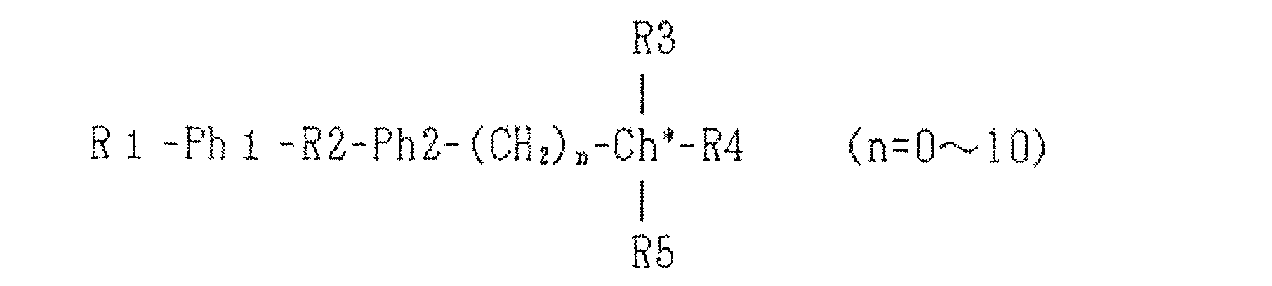
R1、R4は、アミノ基、カルボニル基、カルボキシル基、シアノ基、アミン基、ニトロ基、ニトリル基、およびアルキル鎖のいずれかである。Ph1およびPh2は、フェニル基またはビフェニル基等の芳香族基である。R2は、ビニル基、カルボニル基、カルボキシル基、ジアゾ基、およびアゾキシ基のいずれかである。Ch*はキラル中心を表す。キラル中心は典型的には炭素(C*)である。R3およびR5は、水素、メチル基、アミノ基、カルボニル基、カルボキシル基、シアノ基、アミン基、ニトロ基、ニトリル基、およびアルキル鎖のいずれかである。R3、R4、およびR5は、互いに異なる官能基である。 R1 and R4 are any of an amino group, a carbonyl group, a carboxyl group, a cyano group, an amine group, a nitro group, a nitrile group, and an alkyl chain. Ph1 and Ph2 are aromatic groups such as a phenyl group or a biphenyl group. R2 is any of a vinyl group, a carbonyl group, a carboxyl group, a diazo group, and an azoxy group. Ch * represents the chiral center. The chiral center is typically carbon (C * ). R3 and R5 are any of hydrogen, methyl group, amino group, carbonyl group, carboxyl group, cyano group, amine group, nitro group, nitrile group, and alkyl chain. R3, R4, and R5 are functional groups different from each other.
液晶材料は、組成の異なる複数の液晶分子の混合物であってもよい。例えば、ネマチック液晶分子と、スメクチック液晶分子との混合物を光導波層20の材料として用いてもよい。
The liquid crystal material may be a mixture of a plurality of liquid crystal molecules having different compositions. For example, a mixture of nematic liquid crystal molecules and smectic liquid crystal molecules may be used as the material of the
図63および図65の構成例を、第1のミラー30と、それ以外の構成とを貼り合わせることによって形成してもよい。これにより、製造が容易になる。また、スペーサ73が固体材料であれば、第1のミラー30を蒸着またはスパッタリングなどの方法によって形成してもよい。
The configuration examples of FIGS. 63 and 65 may be formed by laminating the
図61、図63および図65の構成例において、第2のミラー40が複数の導波路素子10によって共用されていることを前提に、第1のミラー30の構成を説明した。当然、上記の議論は、第2のミラー40にも適用できる。すなわち、Y方向において、第1および第2のミラー30および40の少なくとも一方の幅が、光導波層20の幅よりも長ければ、光導波層20からのエバネッセント光の漏れ出しを抑制することができる。その結果、光スキャンに用いられる光量の低下は抑制される。
In the configuration examples of FIGS. 61, 63, and 65, the configuration of the
<応用例>
図67は、回路基板(すなわち、チップ)上に光分岐器90、導波路アレイ10A、位相シフタアレイ80A、および光源130などの素子を集積した光スキャンデバイス100の構成例を示す図である。光源130は、例えば、半導体レーザーなどの発光素子であり得る。この例における光源130は、自由空間における波長がλである単一波長の光を出射する。光分岐器90は、光源130からの光を分岐して複数の位相シフタにおける導波路に導入する。図67の構成例において、チップ上には電極62aと、複数の電極62bとが設けられている。導波路アレイ10Aには、電極62aから制御信号が供給される。位相シフタアレイ80Aにおける複数の位相シフタ80には、複数の電極62bから制御信号がそれぞれ送られる。電極62a、62bは、上記の制御信号を生成する不図示の制御回路に接続され得る。制御回路は、図67に示すチップ上に設けられていてもよいし、光スキャンデバイス100における他のチップに設けられていてもよい。
<Application example>
FIG. 67 is a diagram showing a configuration example of an
図67に示すように、全てのコンポーネントをチップ上に集積することで、小型のデバイスで広範囲の光スキャンが実現できる。例えば2mm×1mm程度のチップに、図67に示される全てのコンポーネントを集積することができる。 As shown in FIG. 67, by integrating all the components on a chip, a wide range of optical scans can be realized with a small device. For example, all the components shown in FIG. 67 can be integrated on a chip having a size of about 2 mm × 1 mm.
図68は、光スキャンデバイス100から遠方にレーザーなどの光ビームを照射して2次元スキャンを実行している様子を示す模式図である。2次元スキャンは、ビームスポット(すなわち、光スポット)310を水平および垂直方向に移動させることによって実行される。例えば、公知のTOF(Time Of Flight)法と組み合わせることで、2次元の測距画像を取得することができる。TOF法は、レーザーを照射して対象物からの反射光を観測することで、光の飛行時間を算出し、距離を求める方法である。
FIG. 68 is a schematic diagram showing a state in which a light beam such as a laser is irradiated far from the
図69は、そのような測距画像を生成することが可能な光検出システムの一例であるライダー(LiDAR)システム300の構成例を示すブロック図である。ライダーシステム300は、光スキャンデバイス100と、光検出器400と、信号処理回路600と、制御回路500とを備えている。光検出器400は、光スキャンデバイス100から出射され、対象物から反射された光を検出する。光検出器400は、例えば光スキャンデバイス100から出射される光の波長λに感度を有するイメージセンサ、またはフォトダイオードなどの受光素子を含むフォトディテクタであり得る。光検出器400は、受光した光の量に応じた電気信号を出力する。信号処理回路600は、光検出器400から出力された電気信号に基づいて、対象物までの距離を計算し、距離分布データを生成する。距離分布データは、距離の2次元分布を示すデータ(すなわち、測距画像)である。制御回路500は、光スキャンデバイス100、光検出器400、および信号処理回路600を制御するプロセッサである。制御回路500は、光スキャンデバイス100からの光ビームの照射のタイミングおよび光検出器400の露光および信号読出しのタイミングを制御し、信号処理回路600に、測距画像の生成を指示する。
FIG. 69 is a block diagram showing a configuration example of a lidar (LiDAR)
2次元スキャンにおいて、測距画像を取得するフレームレートとして、例えば一般的に動画でよく使われる60fps、50fps、30fps、25fps、24fpsなどから選択することができる。また、車載システムへの応用を考慮すると、フレームレートが大きいほど測距画像を取得する頻度が上がり、精度よく障害物を検知できる。例えば、60km/hでの走行時において、60fpsのフレームレートでは車が約28cm移動するごとに画像を取得することができる。120fpsのフレームレートでは、車が約14cm移動するごとに画像を取得することができる。180fpsのフレームレートでは車が、約9.3cm移動するごとに、画像を取得することができる。 In the two-dimensional scan, the frame rate for acquiring the distance measurement image can be selected from, for example, 60 fps, 50 fps, 30 fps, 25 fps, 24 fps and the like, which are generally used in moving images. Further, considering the application to an in-vehicle system, the higher the frame rate, the higher the frequency of acquiring the distance measurement image, and the more accurately the obstacle can be detected. For example, when traveling at 60 km / h, an image can be acquired every time the car moves about 28 cm at a frame rate of 60 fps. At a frame rate of 120 fps, an image can be acquired every time the car moves about 14 cm. At a frame rate of 180 fps, an image can be acquired every time the car moves about 9.3 cm.
1つの測距画像を取得するために必要な時間は、ビームスキャンの速度に依存する。例えば、解像点数が100×100のイメージを60fpsで取得するためには1点につき1.67μs以下でビームスキャンをする必要がある。この場合、制御回路500は、600kHzの動作速度で、光スキャンデバイス100による光ビームの出射、および光検出器400による信号蓄積・読出しを制御する。
The time required to acquire one ranging image depends on the speed of the beam scan. For example, in order to acquire an image having a resolution of 100 × 100 at 60 fps, it is necessary to perform a beam scan at 1.67 μs or less for each point. In this case, the
<光受信デバイスへの応用例>
本開示における光スキャンデバイスは、ほぼ同一の構成で、光受信デバイスとしても用いることができる。光受信デバイスは、光スキャンデバイスと同一の導波路アレイ10Aと、受信可能な光の方向を調整する第1調整素子60とを備える。導波路アレイ10Aの各第1のミラー30は、第3の方向から第1の反射面の反対側に入射する光を透過させる。導波路アレイ10Aの各光導波層20は、第2の方向に第1のミラー30を透過した光を伝搬させる。第1調整素子60が各導波路素子10における前記光導波層20の屈折率および厚さの少なくとも一方を変化させることにより、受信可能な光の方向を変化させることができる。さらに、光受信デバイスが、光スキャンデバイスと同一の複数の位相シフタ80、または80aおよび80bと、複数の導波路素子10から複数の位相シフタ80、または80aおよび80bを通過して出力される光の位相の差をそれぞれ変化させる第2調整素子を備えている場合には、受信可能な光の方向を2次元的に変化させることができる。
<Application example to optical receiving device>
The optical scanning device in the present disclosure has almost the same configuration and can also be used as an optical receiving device. The optical receiving device includes the
例えば図67に示す光スキャンデバイス100における光源130を受信回路に置換した光受信デバイスを構成することができる。導波路アレイ10Aに波長λの光が入射すると、その光は位相シフタアレイ80Aを通じて光分岐器90へ送られ、最終的に一箇所に集められ、受信回路に送られる。その一箇所に集められた光の強度は、光受信デバイスの感度を表すといえる。光受信デバイスの感度は、導波路アレイおよび位相シフタアレイ80Aに別々に組み込まれた調整素子によって調整することができる。光受信デバイスでは、例えば図26において、波数ベクトル(太い矢印)の方向が反対になる。入射光は、導波路素子10が延びる方向(X方向)の光成分と、導波路素子10の配列方向(Y方向)の光成分とを有している。X方向の光成分の感度は、導波路アレイ10Aに組み込まれた調整素子によって調整できる。一方、導波路素子10の配列方向の光成分の感度は、位相シフタアレイ80Aに組み込まれた調整素子によって調整できる。光受信デバイスの感度が最大になるときの光の位相差Δφ、光導波層20の屈折率nwおよび厚さdから、θおよびα0(式(16)および式(17))がわかる。このため、光の入射方向を特定することができる。
For example, an optical receiving device in which the
上述した実施形態および変形例は、適宜、組み合わせることができる。例えば、図61に示した第1のミラー30を他の実施例または変形例の第1のミラー30の代わりに用いてもよい。また、図65に示した導波路素子10を他の実施例または変形例の導波路素子10の代わりに用いてもよい。
The above-described embodiments and modifications can be combined as appropriate. For example, the
<光スキャンをより効率的に行うための実施形態>
次に、光スキャンをより効率的に行うための実施形態を説明する。
<Embodiment for More Efficient Optical Scan>
Next, an embodiment for performing optical scanning more efficiently will be described.
本実施形態における光スキャンデバイスは、導波路アレイと、位相シフタアレイと、第1調整素子と、第2調整素子と、制御回路とを備える。導波路アレイ、位相シフタアレイ、第1調整素子、および第2調整素子の構成は、上述した通りである。制御回路は、第1調整素子および第2調整素子を制御して、導波路アレイから出射される光によって対象領域のスキャンを行う。 The optical scan device in this embodiment includes a waveguide array, a phase shifter array, a first adjusting element, a second adjusting element, and a control circuit. The configurations of the waveguide array, the phase shifter array, the first adjusting element, and the second adjusting element are as described above. The control circuit controls the first adjusting element and the second adjusting element, and scans the target area by the light emitted from the waveguide array.
第1調整素子は、各導波路素子における光導波層の屈折率および厚さの少なくとも一方を変化させることにより、導波路アレイから出射される光の波数ベクトルの、第2の方向(X方向)の成分を変化させる。第2調整素子は、複数の導波路素子のうちの隣接する2つの導波路素子に供給される光の位相差を変化させることにより、導波路アレイから出射される光の波数ベクトルの、第1の方向(Y方向)の成分を変化させる。より具体的には、第2調整素子は、各位相シフタにおける導波路の屈折率を調整することにより、その導波路から出力される光の位相を変化させる。 The first adjusting element changes at least one of the refractive index and the thickness of the optical waveguide layer in each waveguide element in the second direction (X direction) of the wave vector of the light emitted from the waveguide array. Change the composition of. The second adjusting element is the first wave vector of the light emitted from the waveguide array by changing the phase difference of the light supplied to two adjacent waveguide elements among the plurality of waveguide elements. The component in the direction (Y direction) is changed. More specifically, the second adjusting element changes the phase of the light output from the waveguide by adjusting the refractive index of the waveguide in each phase shifter.
本発明者らの検討によれば、光の出射方向をX方向に沿って変化させる場合と、Y方向に沿って変化させる場合とでは、一般に、動作速度に差が生じる。これは、各導波路素子における光導波層、および各位相シフタにおける導波路の構成(材料およびサイズ等)が、一般に異なることに起因している。例えば、導波路の屈折率を変調する方法として、キャリア注入効果、電気光学効果、液晶の複屈折効果、および熱光学効果のいずれの効果を利用するかによって応答速度が大きく異なる。各導波路素子における光導波層、および各位相シフタにおける導波路の屈折率等を調整する際には、それぞれの動作速度を考慮して個別に調整することが望ましい。また、各導波路素子における光導波層、および各位相シフタにおける導波路に与える電圧値および電流値も、それらの構造に応じて適宜設定することが望ましい。そこで、本実施形態における第1調整素子および第2調整素子は、異なる駆動回路によって駆動される。 According to the studies by the present inventors, there is generally a difference in operating speed between the case where the light emission direction is changed along the X direction and the case where the light emission direction is changed along the Y direction. This is due to the fact that the optical waveguide layer in each waveguide element and the waveguide configuration (material, size, etc.) in each phase shifter are generally different. For example, the response speed varies greatly depending on which of the carrier injection effect, the electro-optic effect, the birefringence effect of the liquid crystal, and the thermo-optical effect is used as the method for modulating the refractive index of the waveguide. When adjusting the refractive index of the optical waveguide layer in each waveguide element and the refractive index of the waveguide in each phase shifter, it is desirable to adjust them individually in consideration of their respective operating speeds. Further, it is desirable that the voltage value and the current value applied to the optical waveguide layer in each waveguide element and the waveguide in each phase shifter are appropriately set according to their structures. Therefore, the first adjusting element and the second adjusting element in this embodiment are driven by different drive circuits.
本実施形態における制御回路は、対象領域のスキャンを完了するまでに、第1および第2の方向のうち、スキャン速度が低い方向よりもスキャン速度が高い方向に、導波路アレイによって形成される光スポットを大きく移動させる。ここで「スキャン速度」とは、光スキャンデバイスから所定の距離だけ離れた平面を想定したときに、その平面に形成される光スポットがその平面に沿って移動するときの速度の平均値または最高値を意味する。第1の方向におけるスキャン速度は、各位相シフタにおける導波路の屈折率変調の機構に依存する。第2の方向におけるスキャン速度は、各導波路素子における導波路(光導波層)の屈折率または厚さの変調の機構に依存する。制御回路は、対象領域のスキャンの開始から終了までの間に、第1の方向および第2の方向のうち、スキャン速度が高い方向の成分の移動距離またはステップ数が大きくなるように第1および第2調整素子を制御する。これにより、対象領域全体をスキャンする時間を短縮することができる。 In the control circuit of the present embodiment, the light formed by the waveguide array in the first and second directions in which the scanning speed is higher than the direction in which the scanning speed is low by the time the scanning of the target area is completed. Move the spot a lot. Here, the "scan speed" is the average value or the maximum speed at which a light spot formed on a plane moves along the plane, assuming a plane separated from the optical scanning device by a predetermined distance. Means a value. The scan rate in the first direction depends on the mechanism of refractive index modulation of the waveguide in each phase shifter. The scan rate in the second direction depends on the mechanism of modulation of the refractive index or thickness of the waveguide (optical waveguide layer) in each waveguide element. From the start to the end of the scan of the target area, the control circuit sets the first and second directions so that the movement distance or the number of steps of the component in the direction having the higher scan speed becomes larger in the first direction and the second direction. The second adjusting element is controlled. As a result, the time for scanning the entire target area can be shortened.
図70は、本実施形態における光スキャンデバイス100の構成例を示すブロック図である。光スキャンデバイス100は、導波路アレイ10Aと、第1調整素子60と、位相シフタアレイ80Aと、第2調整素子61と、制御回路500とを備える。導波路アレイ10A、位相シフタアレイ80A、第1調整素子60、および第2調整素子61の構成および機能は、既に説明したとおりである。制御回路500は、第1駆動回路510と、第2駆動回路520と、クロック信号発生器530とを含む。第1駆動回路510は、第1調整素子60を駆動することにより、光を第2の方向(X方向)に沿ってスキャンする。第2駆動回路520は、第2調整素子61を駆動することにより、光を第1の方向(Y方向)に沿ってスキャンする。2次元の光スキャンを制御するために、制御回路500は、クロック信号発生器530によって第1駆動回路510および第2調整素子520を同期して動作させる。クロック信号発生器530は、一定の時間間隔で発するクロック信号に合わせて、第1駆動回路510および第2駆動回路520を駆動する。
FIG. 70 is a block diagram showing a configuration example of the
なお、本実施形態では、図69に示す例とは異なり、光スキャンデバイス100が制御回路500を備えているものとして取り扱う。図69に示すように、制御回路500は、光スキャンデバイス100の外部の要素であってもよい。図70に示す光スキャンデバイス100の全ての構成要素が同一の筐体に収容されている必要はない。
In this embodiment, unlike the example shown in FIG. 69, the
制御回路500は、図68に例示するように、光スキャンデバイス100から所定の距離だけ離れた平面に形成される光スポット310を、例えばX方向およびY方向に沿って移動させる。この際、制御回路500は、予め設定された経路に沿って光スポット310を移動させることにより、対象領域(図68における矩形領域)の全体のスキャンを行う。本実施形態では、スキャン速度の高い方向の総移動距離(またはステップ数)が、スキャン速度の低い方向の総移動距離(またはステップ数)よりも大きくなるようにスキャンされる。これにより、スキャンに要する時間を短縮することができる。なお、対象領域は、必ずしも矩形領域である必要はない。
As illustrated in FIG. 68, the
図71は、1回の対象領域のスキャンにおいて光スポット310が辿る経路の一例を示している。この例では、X方向におけるスキャン速度は、Y方向におけるスキャン速度よりも高い。制御回路500は、光スポットをX方向に大きく移動させ、Y方向には小さく移動させる動作を繰り返す。これにより、光スポット310はジグザグに移動し、対象領域全体がスキャンされる。
FIG. 71 shows an example of the path followed by the
ここで、X方向における対象領域の長さをLXとし、Y方向における対象領域の長さをLYとする。X方向における光スポット310の幅をΔX(<<LX)とし、Y方向における光スポット310の幅をΔY(<<LY)とする。スキャンの単位ステップあたり、X方向にΔX、またはY方向にΔYだけ光スポットが移動するとする。また、nX=LX/ΔX、nY=LY/ΔYとする。さらに、光スポットを±X方向にΔXだけ(1ステップ)移動させるのに、tX秒を要し、光スポットを±Y方向にΔYだけ(1ステップ)移動させるのに、tY秒を要するとする。各導波路素子10における光導波層20、および各位相シフタ80における導波路20aの構成が異なることから、本実施形態では、tXおよびtYは異なる。
Here, the length of the target area in the X direction is LX, and the length of the target area in the Y direction is LY. The width of the
本実施形態では、tXおよびtYがそれぞれ一定であるものとする。このため、スキャン速度は、1秒間当たりのステップ数であると考えることができる。すなわち、X方向におけるスキャン速度は1/tX(ステップ/秒)であり、Y方向におけるスキャン速度は1/tY(ステップ/秒)であると考えることができる。よって、tX>tYの場合、Y方向(第1の方向)におけるスキャン速度が、X方向(第2の方向)におけるスキャン速度よりも高いと言える。逆に、tX<tYの場合、X方向(第2の方向)におけるスキャン速度が、Y方向(第1の方向)におけるスキャン速度よりも高いと言える。対象領域内のX方向およびY方向のそれぞれにおけるスキャン速度が一定でない場合、各方向のスキャンの平均速度または最高速度をスキャン速度と考えればよい。スキャン速度は、ビーム角度の時間変化率(角速度)によって評価することもできる。 In this embodiment, it is assumed that t X and t Y are constant. Therefore, the scan speed can be considered to be the number of steps per second. That is, it can be considered that the scan speed in the X direction is 1 / t X (step / sec) and the scan speed in the Y direction is 1 / t Y (step / sec). Therefore, when t X > t Y , it can be said that the scan speed in the Y direction (first direction) is higher than the scan speed in the X direction (second direction). On the contrary, when t X <t Y , it can be said that the scan speed in the X direction (second direction) is higher than the scan speed in the Y direction (first direction). When the scan speed in each of the X direction and the Y direction in the target area is not constant, the average speed or the maximum speed of the scan in each direction may be considered as the scan speed. The scan speed can also be evaluated by the time change rate (angular velocity) of the beam angle.
図71に示す例では、制御回路500は、対象領域のスキャンを完了するまでに、以下の動作を複数回繰り返す。
(1)光スキャンデバイス100から所定の距離だけ離れた平面に形成される光スポット310を、+X方向に沿って第1の距離(この例ではLX-ΔX=(nX-1)ΔX)だけ移動させる。
(2)光スポット310を、-Y方向に沿って第1の距離よりも短い第2の距離(この例ではΔY)だけ移動させる。
(3)光スポット310を、-X方向に沿って第1の距離だけ移動させる。
(4)光スポット310を、-Y方向に沿って第2の距離だけ移動させる。
In the example shown in FIG. 71, the
(1) An
(2) The
(3) The
(4) The
以上の動作により、スキャン速度の高いX方向への光スポットの総移動距離が、Y方向への総移動距離よりも長くなる。このため、対象領域の1回のスキャンに要する時間を短くすることができる。 By the above operation, the total moving distance of the light spot in the X direction, which has a high scanning speed, becomes longer than the total moving distance in the Y direction. Therefore, the time required for one scan of the target area can be shortened.
なお、上記の動作において、+X方向と-X方向とは逆でもよい。また、-Y方向への移動に代えて、+Y方向への移動を行ってもよい。言い換えれば、制御回路500は、以下の動作を2回以上行ってもよい。
(1)光スキャンデバイス100から所定の距離だけ離れた平面に形成される光スポット310を、+X方向および-X方向の一方に沿って、第1の距離だけ移動させる。
(2)光スポット310を、+Y方向および-Y方向の一方に沿って、第1の距離よりも短い第2の距離だけ移動させる。
(3)光スポット310を、+X方向および-X方向の他方に沿って、第1の距離だけ移動させる。
(4)光スポット310を、+Y方向および-Y方向の前記一方に沿って、第2の距離だけ移動させる。
In the above operation, the + X direction and the −X direction may be opposite to each other. Further, instead of moving in the −Y direction, movement in the + Y direction may be performed. In other words, the
(1) The
(2) The
(3) The
(4) The
ここで、図71の例における対象領域の1フレーム当たりのスキャン時間TXYを検討する。1フレーム当たりのスキャンにおいて、光スポット310を+X方向または-X方向に(nX-1)ステップ移動させて1つのラインをスキャンする動作が、nY回行われる。さらに、光スポット310を-Y方向に1ステップ移動させる動作が、(nY-1)回行われる。したがって、TXY=tX(nX-1)nY+tY(nY-1)秒となる。
Here, the scan time TXY per frame of the target area in the example of FIG. 71 is examined. In scanning per frame, the operation of moving the
図72は、1回の対象領域のスキャンにおいて光スポット310が辿る経路の他の例を示している。この例は、X方向(第2の方向)におけるスキャン速度よりもY方向(第1の方向)におけるスキャン速度の方が高い場合の例である。制御回路500は、対象領域のスキャンを完了するまでに、以下の動作を複数回繰り返す。
(1)光スキャンデバイス100から所定の距離だけ離れた平面に形成される光スポット310を、-Y方向に沿って第1の距離(この例ではLy-ΔY=(nY-1)ΔY)だけ移動させる。
(2)光スポット310を、+X方向に沿って第1の距離よりも短い第2の距離(この例ではΔX)だけ移動させる。
(3)光スポット310を、+Y方向に沿って第1の距離だけ移動させる。
(4)光スポット310を、+X方向に沿って第2の距離だけ移動させる。
FIG. 72 shows another example of the path followed by the
(1) An
(2) The
(3) The
(4) The
以上の動作により、スキャン速度の高いY方向への光スポットの総移動距離が、X方向への総移動距離よりも長くなる。このため、対象領域の1回のスキャンに要する時間を短くすることができる。 By the above operation, the total moving distance of the light spot in the Y direction, which has a high scanning speed, becomes longer than the total moving distance in the X direction. Therefore, the time required for one scan of the target area can be shortened.
なお、上記の動作において、+Y方向と-Y方向とは逆でもよい。また、+X方向への移動に代えて、-Y方向への移動を行ってもよい。言い換えれば、制御回路500は、以下の動作を2回以上行ってもよい。
(1)光スキャンデバイス100から所定の距離だけ離れた平面に形成される光スポット310を、+Y方向および-Y方向の一方に沿って第1の距離だけ移動させる。
(2)光スポット310を、+X方向および-X方向の一方に沿って第1の距離よりも短い第2の距離だけ移動させる。
(3)光スポット310を、+Y方向および-Y方向の他方に沿って第1の距離だけ移動させる。
(4)光スポット310を、+X方向および-X方向の前記一方に沿って第2の距離だけ移動させる。
In the above operation, the + Y direction and the −Y direction may be opposite to each other. Further, instead of moving in the + X direction, movement in the −Y direction may be performed. In other words, the
(1) The
(2) The
(3) The
(4) The
ここで、図72の例における対象領域の1フレーム当たりのスキャン時間TYXを検討する。1フレーム当たりのスキャンにおいて、光スポット310を+Y方向または-Y方向に(nY-1)ステップ移動させて1つのラインをスキャンする動作が、nX回行われる。さらに、光スポット310を+X方向に1ステップ移動させる動作が(nX-1)回行われる。したがって、TYX=tX(nX-1)+tYnX(nY-1)秒となる。
Here, the scan time TYX per frame of the target area in the example of FIG. 72 is examined. In scanning per frame, the operation of moving the
図71および図72における対象領域の1フレーム当たりのスキャン時間を比較する。例えば、TXY>TYX(TXY-TYX>0)となる条件は、TXY-TYX=(tX-tY)(nX‐1)(nY‐1)>0から、tX>tYとなる。したがって、Y方向におけるスキャン速度が、X方向におけるスキャン速度よりも高い場合、図72に示すように、光スポット310をX方向よりもY方向に大きく移動させることによって、1フレーム当たりのスキャン時間を短くする効果が得られる。逆に、X方向におけるスキャン速度が、Y方向におけるスキャン速度よりも高い場合、図71に示すように、光スポット310をY方向よりもX方向に大きく移動させることによって、1フレーム当たりのスキャン時間を短くする効果が得られる。
The scan times per frame of the target area in FIGS. 71 and 72 are compared. For example, the condition that T XY > T YY (T XY-TYX> 0) is from T XY-T YX = ( t X - t Y ) (n X -1) (n Y -1)> 0. t X > t Y. Therefore, when the scan speed in the Y direction is higher than the scan speed in the X direction, as shown in FIG. 72, the
上記の効果を得るために、本実施形態における制御回路500は、対象領域のスキャンを完了するまでに、X方向およびY方向のうち、スキャン速度が高い方向に、光スキャンデバイス100によって形成される光スポットをより大きく移動させる。これにより、全体のスキャン時間を短くすることができる。
In order to obtain the above effects, the
次に、対象領域の2次元スキャン動作の変形例を説明する。以下の変形例では、X方向におけるスキャン速度が、Y方向におけるスキャン速度よりも高い場合を扱う。同様の制御は、Y方向におけるスキャン速度が、X方向におけるスキャン速度よりも高い場合にも適用できる。 Next, a modified example of the two-dimensional scanning operation of the target area will be described. The following modification deals with the case where the scan speed in the X direction is higher than the scan speed in the Y direction. Similar controls can be applied when the scan speed in the Y direction is higher than the scan speed in the X direction.
図73は、2次元スキャン動作の変形例を示す図である。図71における動作とは異なり、制御回路500は、1つの行のスキャンを行うと、次の行に移り、先の行とは逆方向にスキャンする、という動作を繰り返す。X方向または-X方向に連続で移動する距離である第1の距離は(Lx-ΔX)よりも短い。光スポット310が対象領域の上下の端に到達した場合、制御回路500は、まだスキャンしていない複数の列について、折り返して同様の2次元スキャンを続ける。
FIG. 73 is a diagram showing a modified example of the two-dimensional scanning operation. Unlike the operation in FIG. 71, the
この例においても、Y方向よりもX方向の総移動距離が長くなるため、X方向のスキャン速度がY方向のスキャン速度よりも高い場合、全体のスキャン時間を短くすることができる。 Also in this example, since the total movement distance in the X direction is longer than that in the Y direction, when the scan speed in the X direction is higher than the scan speed in the Y direction, the entire scan time can be shortened.
図74は、0次および±1次回折光を用いた2次元スキャンの一例を示す図である。導波路アレイ10Aが出射する光には、0次光(0次回折光とも称する)だけでなく、±1次回折光などの回折光も含まれる。この例における制御回路500は、導波路アレイ10Aから出射される0次および±1次回折光によって、対象領域のスキャンを行う。図71における2次元スキャンと比較して、図74における2次元スキャンでは、0次および±1次回折光を用いることによって対象領域全体のスキャンに要する時間を短縮することができる。この例における制御回路500は、対象領域をX方向に3分割した3つの領域を、0次回折光、+1次回折光、-1次回折光にそれぞれ割り当ててスキャンする。これにより、対象領域全体のスキャンに要する時間が約1/3に低減し、効率よくスキャンすることが可能となる。
FIG. 74 is a diagram showing an example of a two-dimensional scan using 0th-order and ± 1st-order diffracted light. The light emitted by the
以上の各例では、光スポットは常にX方向(横方向とも称する)またはY方向(縦方向とも称する)に沿って移動するが、本開示はそのような例に限定されない。例えば、対象領域をスキャンする際の光スポットの経路の一部に、斜め方向に移動する経路が含まれていてもよい。 In each of the above examples, the light spot always moves along the X direction (also referred to as the horizontal direction) or the Y direction (also referred to as the vertical direction), but the present disclosure is not limited to such an example. For example, a path that moves in an oblique direction may be included as a part of the path of the light spot when scanning the target area.
図75は、対象領域全体を斜め方向にスキャンする動作の一例を示す図である。この例における制御回路500は、対象領域のスキャンを完了するまでに、以下の動作を2回以上繰り返す。
(1)光スキャンデバイス100から所定の距離だけ離れた平面に形成される光スポット310を、+X方向および-X方向の一方に沿って(この例では+X方向)、第1の距離(この例ではLx-ΔX)だけ移動させると同時に、光スポット310を、+Y方向および-Y方向の一方に沿って(この例では-Y方向)、第1の距離よりも短い第2の距離(この例ではΔY)だけ移動させる。
(2)光スポット310を、+X方向および-X方向の他方に沿って(この例では-X方向)、第1の距離だけ移動させると同時に、光スポット310を、+Y方向および-Y方向の上記の一方に沿って(この例では-Y方向)、第2の距離だけ移動させる。
FIG. 75 is a diagram showing an example of an operation of scanning the entire target area in an oblique direction. The
(1) An
(2) The
横方向および縦方向のスキャンを同時に行うことにより、斜め方向のスキャンが可能となる。このような動作によっても、対象領域のスキャンが可能である。 By performing horizontal and vertical scans at the same time, diagonal scans are possible. Even by such an operation, it is possible to scan the target area.
図76は、対象領域の端における折り返しの前後だけ、斜め方向にスキャンする動作の一例を示す図である。この例では、光スポット310が、対象領域の端(この例では左右の端)から第1の距離(この例では2ΔX)の範囲内に位置する場合は、折り返すために
斜めに移動する。それ以外の場合はX軸に沿って移動する。この例では、折り返しの前後におけるY方向の移動距離である第2の距離はΔY/2である。
FIG. 76 is a diagram showing an example of an operation of scanning in an oblique direction only before and after folding at the edge of the target area. In this example, if the
次に、本実施形態における各導波路素子10における光導波層20、および第1調整素子の構成と、各位相シフタにおける導波路20a、および第2調整素子の構成とを説明する。
Next, the configuration of the
本実施形態における各導波路素子10における光導波層20は、電圧が印加された場合に、光導波層20を伝搬する光に対する屈折率が変化する材料を含む。第1調整素子は、各導波路素子10における光導波層20を挟む第1の一対の電極62を備え、第1の一対の電極62に電圧を印加することにより、光導波層20の屈折率を変化させる。このような構成は、例えば、図32A~図32Cに示されている。
The
同様に、各位相シフタ80における導波路20aは、電圧が印加された場合に、導波路20aを伝搬する光に対する屈折率が変化する材料を含む。第2調整素子は、各位相シフタ80における導波路20aを挟む第2の一対の電極62bを備え、第2の一対の電極62bに電圧を印加することにより、導波路20aの屈折率を変化させる。
Similarly, the
図77Aは、第2調整素子61の構成の一例を模式的に示す斜視図である。図77Bは、第2調整素子61の構成の他の例を模式的に示す斜視図である。図77Cは、第2調整素子61の構成のさらに他の例を模式的に示す斜視図である。図77A~77Cに示された構成は、それぞれ図32A~図32Cに示された構成において、第1および第2のミラー30、40を除去して、各導波路素子10における光導波層20を、各位相シフタ80における導波路20aに置き換えた構成に相当する。電源66bをオンにして配線64bを通じて第2の一対の電極62bに電圧を印加することで、導波層20aの屈折率を調整することができる。
FIG. 77A is a perspective view schematically showing an example of the configuration of the
一例として、各導波路素子10における光導波層20が電気光学材料を含む場合、導波路素子10における光導波層20の屈折率は、1GHzまたはそれ以上のオーダーで変化する。このとき、各位相シフタ80における導波路20aの屈折率が、キャリア注入または熱光学効果のいずれによって変化しても、各導波路素子10における光導波層20の屈折率の方がより速く変化する。
As an example, when the
他の例として、各導波路素子10における光導波層20が液晶材料を含む場合、各導波路素子10における光導波層20の屈折率は、10Hz~1kHz程度のオーダーで変化する。このとき、各位相シフタ80における導波路20aの屈折率が、キャリア注入、熱光学効果または電気光学材料のいずれによって変化しても、各位相シフタ80における導波路20aの屈折率の方がより速く変化する。
As another example, when the
したがって、本実施形態においては、光導波層20の屈折率変化の速さと、導波路20aの屈折率変化の速さとの大小関係に応じて、トータルのスキャン時間が短くなるようにスキャンの経路が決定される。
Therefore, in the present embodiment, the scanning path is set so that the total scanning time is shortened according to the magnitude relationship between the speed of change in the refractive index of the
以下に、各導波路素子10における光導波層20、および各位相シフタ80における導波路20aの材料の組み合わせの例を示す。
The following is an example of the combination of the materials of the
まず、各導波路素子10における光導波層20が、電気光学材料を含み、各位相シフタ80における導波路20aが、液晶材料を含む例を説明する。第1調整素子は、第1の一対の電極に電圧を印加することにより、光導波層20の屈折率を変化させる。第2調整素子は、第2の一対の電極に電圧を印加することにより、液晶材料の屈折率異方性を変化させ、導波路の屈折率を変化させる。この例では、X方向におけるスキャン速度は、Y方向におけるスキャン速度よりも高い。したがって、制御回路500は、Y方向よりもX方向に大きく光スポットを移動させるような経路で、対象領域のスキャンを行う。
First, an example will be described in which the
次に、各導波路素子10における光導波層20が、液晶材料を含み、各位相シフタ80における導波路20aが、電気光学材料を含む例を説明する。第1調整素子は、第1の一対の電極に電圧を印加することにより、液晶材料の屈折率異方性を変化させ、光導波層20の屈折率を変化させる。第2調整素子は、第2の一対の電極に電圧を印加することにより、導波路の屈折率を変化させる。この例では、Y方向におけるスキャン速度は、X方向におけるスキャン速度よりも高い。したがって、制御回路500は、X方向よりもY方向に大きく光スポットを移動させるような経路で、対象領域のスキャンを行う。
Next, an example will be described in which the
次に、各導波路素子10における光導波層20が、半導体材料を含み、各位相シフタ80における導波路20aが、液晶材料を含む例を説明する。第1の一対の電極の一方、または第1の一対の電極の一方と光導波層20との間には、p型半導体が含まれ、第1の一対の電極の他方、または第1の一対の電極の他方と光導波層20との間には、n型半導体が含まれる。第1調整素子は、第1の一対の電極に電圧を印加することにより、半導体材料にキャリアを注入し、光導波層20の屈折率を変化させる。第2調整素子は、第2の一対の電極に電圧を印加することにより、液晶材料の屈折率異方性を変化させ、導波路の屈折率を変化させる。この例では、X方向におけるスキャン速度は、Y方向におけるスキャン速度よりも高い。したがって、制御回路500は、Y方向よりもX方向に大きく光スポットを移動させるような経路で、対象領域のスキャンを行う。
Next, an example will be described in which the
最後に、各導波路素子10における光導波層20が、液晶材料を含み、各位相シフタ80における導波路20aが、半導体材料を含む例を説明する。第1調整素子は、第1の一対の電極に電圧を印加することにより、液晶材料の屈折率異方性を変化させ、導波路の屈折率を変化させる。第2の一対の電極の一方、または前記第2の一対の電極の一方と前記導波路との間には、p型半導体が含まれ、第2の一対の電極の他方、または前記第2の一対の電極の他方と前記導波路との間には、n型半導体が含まれる。第2調整素子は、第2の一対の電極に電圧を印加することにより、半導体材料にキャリアを注入し、導波路の屈折率を変化させる。この例では、Y方向におけるスキャン速度は、X方向におけるスキャン速度よりも高い。したがって、制御回路500は、X方向よりもY方向に大きく光スポットを移動させるような経路で、対象領域のスキャンを行う。
Finally, an example will be described in which the
以上のような構成により、本実施形態における光スキャンデバイス100は、対象領域のスキャンに要する時間を短縮することができる。
With the above configuration, the
本開示の実施形態における光スキャンデバイスおよび光受信デバイスは、例えば自動車、UAV、AGVなどの車両に搭載されるライダーシステムなどの用途に利用できる。 The optical scanning device and the optical receiving device according to the embodiment of the present disclosure can be used for applications such as a rider system mounted on a vehicle such as an automobile, a UAV, or an AGV.
1 第1の導波路
2 光導波層、導波路
3 多層反射膜
4 多層反射膜
5 グレーティング
6 レーザー光源
7 光ファイバー
10 導波路素子(第2の導波路)
20 光導波層
30 第1のミラー
40 第2のミラー
42 低屈折率層
44 高屈折率層
50、50A、50B、50C 基板
51 第1の誘電体層(調整層)
52 支持部材(補助基板)
60 調整素子
61 第2の誘電体層(保護層)
62 電極
64 配線
66 電源
68 ヒーター
70 支持部材
71 非圧電素子
72 圧電素子
73、73a、73b スペーサ
74a、74b 支持部材
80、80a、80b 位相シフタ
90、90a、90b 光分岐器
92 光スイッチ
100 光スキャンデバイス
110 導波路アレイの駆動回路
130 光源
210 位相シフタアレイの駆動回路
310 ビームスポット
400 光検出器
500 制御回路
510 第1駆動回路
520 第2駆動回路
530 クロック信号発生器
600 信号処理回路
1
20
52 Support member (auxiliary board)
60 Adjusting
62
Claims (16)
各導波路素子における前記光導波層の屈折率および厚さの少なくとも一方を変化させることにより、前記導波路アレイから前記第3の方向に出射される光の波数ベクトルの、前記第2の方向の成分を変化させる第1調整素子と、
前記複数の導波路素子にそれぞれ接続された複数の位相シフタであって、それぞれが、前記複数の導波路素子の対応する1つにおける前記光導波層に直接的にまたは他の導波路を介して繋がる導波路を含む複数の位相シフタと、
前記複数の位相シフタから前記複数の導波路素子へ伝搬する光の位相の差をそれぞれ変化させることにより、前記導波路アレイから前記第3の方向に出射される光の波数ベクトルの、前記第1の方向の成分を変化させる第2調整素子と、
前記第1調整素子および前記第2調整素子を制御して、前記導波路アレイから出射される光によって対象領域のスキャンを行う制御回路と、
を備え、
各導波路素子は、
前記第3の方向に交差する反射面を有し、前記第2の方向に延びる第1のミラーと、
前記第1のミラーの前記反射面に対向する反射面を有し、前記第2の方向に延びる第2のミラーと、
をさらに備え、
前記光導波層は、前記第1のミラーと前記第2のミラーの間に位置し、
前記第1のミラーは、前記第2のミラーよりも高い光透過率を有し、前記光導波層内を伝搬する光の一部を、前記光導波層の外部に出射し、
前記第1の方向におけるスキャン速度と、前記第2の方向におけるスキャン速度とは異なり、
前記導波路アレイから出射される光によって、前記導波路アレイから離れて配置された前記第1および第2の方向に平行な仮想的な平面に光スポットが形成されるとした場合、前記制御回路は、前記対象領域のスキャンの開始から完了までに、前記第1および第2の方向のうち、前記スキャン速度が低い方向よりも前記スキャン速度が高い方向に前記光スポットを大きく移動させ、
前記制御回路は、前記導波路アレイから出射される0次および少なくとも一本の高次光によって前記対象領域のスキャンを行う、
光スキャンデバイス。 A plurality of waveguide arrays comprising a plurality of waveguide elements arranged in a first direction and each comprising an optical waveguide layer for propagating light in a second direction intersecting the first direction. A waveguide array that emits light from a waveguide element in a third direction intersecting a virtual plane parallel to the first and second directions.
By changing at least one of the refractive index and the thickness of the optical waveguide layer in each waveguide element, the wave vector of the light emitted from the waveguide array in the third direction in the second direction. The first adjusting element that changes the composition and
A plurality of phase shifters, each connected to the plurality of waveguide elements, each directly or via another waveguide in the optical waveguide layer in the corresponding one of the plurality of waveguide elements. Multiple phase shifters, including connected waveguides,
The first wave vector of the light wave vector emitted from the waveguide array in the third direction by changing the phase difference of the light propagating from the plurality of phase shifters to the plurality of waveguide elements. The second adjusting element that changes the component in the direction of
A control circuit that controls the first adjusting element and the second adjusting element to scan the target region by the light emitted from the waveguide array.
Equipped with
Each waveguide element
A first mirror having reflecting surfaces intersecting in the third direction and extending in the second direction.
A second mirror having a reflecting surface facing the reflecting surface of the first mirror and extending in the second direction,
Further prepare
The optical waveguide layer is located between the first mirror and the second mirror .
The first mirror has a higher light transmittance than the second mirror, and a part of the light propagating in the optical waveguide layer is emitted to the outside of the optical waveguide layer.
The scan speed in the first direction is different from the scan speed in the second direction.
When the light emitted from the waveguide array forms an optical spot on a virtual plane parallel to the first and second directions arranged away from the waveguide array, the control circuit. Moves the light spot significantly in the direction in which the scanning speed is higher than the direction in which the scanning speed is lower among the first and second directions from the start to the completion of scanning the target area.
The control circuit scans the target area with zero-order and at least one high-order light emitted from the waveguide array.
Optical scanning device.
前記制御回路は、前記対象領域のスキャンの開始から完了までに、
前記光スポットを、前記第2の方向および前記第2の方向の逆方向の一方に沿って第1の距離だけ移動させ、
前記光スポットを、前記第1の方向および前記第1の方向の逆方向の一方に沿って、前記第1の距離よりも短い第2の距離だけ移動させ、
前記光スポットを、前記第2の方向および前記第2の方向の逆方向の他方に沿って前記第1の距離だけ移動させ、
前記光スポットを、前記第1の方向および前記第1の方向の逆方向の前記一方に沿って前記第2の距離だけ移動させる動作を2回以上繰り返す、
請求項1に記載の光スキャンデバイス。 The scan speed in the second direction is higher than the scan speed in the first direction.
The control circuit is used from the start to the end of scanning the target area.
The light spot is moved by a first distance along one of the second direction and the opposite direction of the second direction.
The light spot is moved along one of the first direction and the opposite direction of the first direction by a second distance shorter than the first distance.
The light spot is moved by the first distance along the other of the second direction and the opposite direction of the second direction.
The operation of moving the light spot by the second distance along the one of the first direction and the opposite direction of the first direction is repeated two or more times.
The optical scanning device according to claim 1.
前記制御回路は、前記対象領域のスキャンの開始から完了までに、
前記光スポットを、前記第1の方向および前記第1の方向の逆方向の一方に沿って第1の距離だけ移動させ、
前記光スポットを、前記第2の方向および前記第2の方向の逆方向の一方に沿って、前記第1の距離よりも短い第2の距離だけ移動させ、
前記光スポットを、前記第1の方向および前記第1の方向の逆方向の他方に沿って前記第1の距離だけ移動させ、
前記光スポットを、前記第2の方向および前記第2の方向の逆方向の前記一方に沿って前記第2の距離だけ移動させる動作を2回以上繰り返す、
請求項1に記載の光スキャンデバイス。 The scan speed in the first direction is higher than the scan speed in the second direction.
The control circuit is used from the start to the end of scanning the target area.
The light spot is moved by a first distance along one of the first direction and the opposite direction of the first direction.
The light spot is moved along one of the second direction and the opposite direction of the second direction by a second distance shorter than the first distance.
The light spot is moved by the first distance along the other of the first direction and the opposite direction of the first direction.
The operation of moving the light spot by the second distance along the one of the second direction and the opposite direction of the second direction is repeated two or more times.
The optical scanning device according to claim 1.
前記制御回路は、前記対象領域のスキャンの開始から完了までに、
前記光スポットを、前記第2の方向および前記第2の方向の逆方向の一方に沿って第1の距離だけ移動させると同時に、前記光スポットを、前記第1の方向および前記第1の方向の逆方向の一方に沿って、前記第1の距離よりも短い第2の距離だけ移動させ、
前記光スポットを、前記第2の方向および前記第2の方向の逆方向の他方に沿って前記第1の距離だけ移動させると同時に、前記光スポットを、前記第1の方向および前記第1の方向の逆方向の前記一方に沿って前記第2の距離だけ移動させる
動作を2回以上繰り返す、
請求項1に記載の光スキャンデバイス。 The scan speed in the second direction is higher than the scan speed in the first direction.
The control circuit is used from the start to the end of scanning the target area.
The light spot is moved by a first distance along one of the second direction and the opposite direction of the second direction, and at the same time, the light spot is moved in the first direction and the first direction. Move along one of the opposite directions by a second distance shorter than the first distance.
The light spot is moved by the first distance along the other of the second direction and the opposite direction of the second direction, and at the same time, the light spot is moved in the first direction and the first direction. The operation of moving by the second distance along the one in the opposite direction is repeated twice or more.
The optical scanning device according to claim 1.
前記制御回路は、前記対象領域のスキャンの開始から完了までに、
前記光スポットを、前記第1の方向および前記第1の方向の逆方向の一方に沿って第1の距離だけ移動させると同時に、前記光スポットを、前記第2の方向および前記第2の方向の逆方向の一方に沿って、前記第1の距離よりも短い第2の距離だけ移動させ、
前記光スポットを、前記第1の方向および前記第1の方向の逆方向の他方に沿って前記第1の距離だけ移動させると同時に、前記光スポットを、前記第2の方向および前記第2の方向の逆方向の前記一方に沿って前記第2の距離だけ移動させる
動作を2回以上繰り返す、
請求項1に記載の光スキャンデバイス。 The scan speed in the first direction is higher than the scan speed in the second direction.
The control circuit is used from the start to the end of scanning the target area.
The light spot is moved by a first distance along one of the first direction and the opposite direction of the first direction, and at the same time, the light spot is moved in the second direction and the second direction. Move along one of the opposite directions by a second distance shorter than the first distance.
The light spot is moved by the first distance along the other of the first direction and the opposite direction of the first direction, and at the same time, the light spot is moved in the second direction and the second direction. The operation of moving by the second distance along the one in the opposite direction is repeated twice or more.
The optical scanning device according to claim 1.
前記第1調整素子は、前記光導波層を挟む第1の一対の電極を備え、前記第1の一対の電極に電圧を印加することにより、前記光導波層の屈折率を変化させ、
各位相シフタにおける前記導波路は、電圧が印加された場合に、前記導波路を伝搬する光に対する屈折率が変化する材料を含み、
前記第2調整素子は、前記導波路を挟む第2の一対の電極を備え、前記第2の一対の電極に電圧を印加することにより、前記導波路の屈折率を変化させ、前記導波路から出力される光の位相を変化させる、請求項1に記載の光スキャンデバイス。 The optical waveguide layer in each waveguide contains a material whose refractive index with respect to light propagating through the optical waveguide layer changes when a voltage is applied.
The first adjusting element includes a first pair of electrodes sandwiching the optical waveguide layer, and by applying a voltage to the first pair of electrodes, the refractive index of the optical waveguide layer is changed.
The waveguide in each phase shifter comprises a material whose refractive index with respect to light propagating through the waveguide changes when a voltage is applied.
The second adjusting element includes a second pair of electrodes that sandwich the waveguide, and by applying a voltage to the second pair of electrodes, the refractive index of the waveguide is changed from the waveguide. The optical scanning device according to claim 1, wherein the phase of the output light is changed.
前記第1調整素子は、前記光導波層を挟む第1の一対の電極を備え、前記第1の一対の電極に電圧を印加することにより、前記光導波層の屈折率を変化させ、
各位相シフタにおける前記導波路は、液晶材料を含み、
前記第2調整素子は、前記導波路を挟む第2の一対の電極を備え、前記第2の一対の電極に電圧を印加することにより、前記液晶材料の屈折率異方性を変化させ、前記導波路の屈折率を変化させて前記導波路から出力される光の位相を変化させる、請求項2または4に記載の光スキャンデバイス。 The optical waveguide layer in each waveguide element contains an electro-optical material.
The first adjusting element includes a first pair of electrodes sandwiching the optical waveguide layer, and by applying a voltage to the first pair of electrodes, the refractive index of the optical waveguide layer is changed.
The waveguide in each phase shifter comprises a liquid crystal material.
The second adjusting element includes a second pair of electrodes that sandwich the waveguide, and by applying a voltage to the second pair of electrodes, the refractive index anisotropy of the liquid crystal material is changed to change the refractive index anisotropy. The optical scan device according to claim 2 or 4 , wherein the refractive index of the waveguide is changed to change the phase of the light output from the waveguide.
前記第1調整素子は、前記光導波層を挟む第1の一対の電極を備え、前記第1の一対の電極に電圧を印加することにより、前記液晶材料の屈折率異方性を変化させ、前記光導波層の屈折率を変化させ、
各位相シフタにおける前記導波路は、電気光学材料を含み、
前記第2調整素子は、前記導波路を挟む第2の一対の電極を備え、前記第2の一対の電極に電圧を印加することにより、前記導波路の屈折率を変化させて前記導波路から出力される光の位相を変化させる、請求項3または5に記載の光スキャンデバイス。 The optical waveguide layer in each waveguide element contains a liquid crystal material.
The first adjusting element includes a first pair of electrodes sandwiching the optical waveguide layer, and by applying a voltage to the first pair of electrodes, the refractive index anisotropy of the liquid crystal material is changed. By changing the refractive index of the optical waveguide layer,
The waveguide in each phase shifter comprises an electro-optical material.
The second adjusting element includes a second pair of electrodes that sandwich the waveguide, and by applying a voltage to the second pair of electrodes, the refractive index of the waveguide is changed from the waveguide. The optical scanning device according to claim 3 or 5 , which changes the phase of the output light.
前記第1調整素子は、前記光導波層を挟む第1の一対の電極を備え、
前記第1の一対の電極の一方、または前記第1の一対の電極の一方と前記光導波層との間には、p型半導体が含まれ、
前記第1の一対の電極の他方、または前記第1の一対の電極の他方と前記光導波層との間には、n型半導体が含まれ、
前記第1調整素子は、前記第1の一対の電極に電圧を印加することにより、前記半導体材料にキャリアを注入し、前記光導波層の屈折率を変化させ、
各位相シフタにおける前記導波路は、液晶材料を含み、
前記第2調整素子は、前記光導波層を挟む第2の一対の電極を備え、前記第2の一対の電極に電圧を印加することにより、前記液晶材料の屈折率異方性を変化させ、前記導波路の屈折率を変化させて前記導波路から出力される光の位相を変化させる、請求項2または4に記載の光スキャンデバイス。 The optical waveguide layer in each waveguide element contains a semiconductor material.
The first adjusting element includes a first pair of electrodes sandwiching the optical waveguide layer.
A p-type semiconductor is included between one of the first pair of electrodes or one of the first pair of electrodes and the optical waveguide layer.
An n-type semiconductor is included between the other of the first pair of electrodes or the other of the first pair of electrodes and the optical waveguide layer.
The first adjusting element injects carriers into the semiconductor material by applying a voltage to the first pair of electrodes to change the refractive index of the optical waveguide layer.
The waveguide in each phase shifter comprises a liquid crystal material.
The second adjusting element includes a second pair of electrodes sandwiching the optical waveguide layer, and by applying a voltage to the second pair of electrodes, the refractive index anisotropy of the liquid crystal material is changed. The optical scan device according to claim 2 or 4 , wherein the refractive index of the waveguide is changed to change the phase of the light output from the waveguide.
前記第1調整素子は、前記光導波層を挟む第1の一対の電極を備え、前記第1の一対の電極に電圧を印加することにより、前記液晶材料の屈折率異方性を変化させ、前記導波路の屈折率を変化させ、
各位相シフタにおける前記導波路は、半導体材料を含み、
前記第2調整素子は、前記光導波層を挟む第2の一対の電極を備え、
前記第2の一対の電極の一方、または前記第2の一対の電極の一方と前記導波路との間には、p型半導体が含まれ、
前記第2の一対の電極の他方、または前記第2の一対の電極の他方と前記導波路との間には、n型半導体が含まれ、
前記第2調整素子は、前記第2の一対の電極に電圧を印加することにより、前記半導体材料にキャリアを注入し、前記導波路の屈折率を変化させて前記導波路から出力される光の位相を変化させる、請求項3または5に記載の光スキャンデバイス。 The optical waveguide layer in each waveguide element contains a liquid crystal material.
The first adjusting element includes a first pair of electrodes sandwiching the optical waveguide layer, and by applying a voltage to the first pair of electrodes, the refractive index anisotropy of the liquid crystal material is changed. By changing the refractive index of the waveguide,
The waveguide in each phase shifter comprises a semiconductor material.
The second adjusting element includes a second pair of electrodes sandwiching the optical waveguide layer.
A p-type semiconductor is included between one of the second pair of electrodes or one of the second pair of electrodes and the waveguide.
An n-type semiconductor is included between the other of the second pair of electrodes or the other of the second pair of electrodes and the waveguide.
The second adjusting element injects carriers into the semiconductor material by applying a voltage to the second pair of electrodes, changes the refractive index of the waveguide, and outputs light from the waveguide. The optical scanning device according to claim 3 or 5 , which changes the phase.
各導波路素子における前記光導波層の屈折率および厚さの少なくとも一方を変化させることにより、前記導波路アレイから前記第3の方向に出射される光の波数ベクトルの、前記第2の方向の成分を変化させる第1調整素子と、
前記複数の導波路素子にそれぞれ接続された複数の位相シフタであって、それぞれが、前記複数の導波路素子の対応する1つにおける前記光導波層に直接的にまたは他の導波路を介して繋がる導波路を含む複数の位相シフタと、
前記複数の位相シフタから前記複数の導波路素子へ伝搬する光の位相の差をそれぞれ変化させることにより、前記導波路アレイから前記第3の方向に出射される光の波数ベクトルの、前記第1の方向の成分を変化させる第2調整素子と、
前記第1調整素子および前記第2調整素子を制御して、前記導波路アレイから出射される光によって対象領域のスキャンを行う制御回路と、
を備え、
各導波路素子は、
前記第3の方向に交差する反射面を有し、前記第2の方向に延びる第1のミラーと、
前記第1のミラーの前記反射面に対向する反射面を有し、前記第2の方向に延びる第2のミラーと、
をさらに備え、
前記光導波層は、前記第1のミラーと前記第2のミラーの間に位置し、可変の厚さおよび/または前記光に対する可変の屈折率を有し、
前記第1のミラーは、前記第2のミラーよりも高い光透過率を有し、前記光導波層内を伝搬する光の一部を、前記光導波層の外部に出射し、
前記第1の方向におけるスキャン速度と、前記第2の方向におけるスキャン速度とは異なり、
前記導波路アレイから出射される光によって、前記導波路アレイから離れて配置された前記第1および第2の方向に平行な仮想的な平面に光スポットが形成されるとした場合、前記制御回路は、前記対象領域のスキャンの開始から完了までに、前記第1および第2の方向のうち、前記スキャン速度が低い方向よりも前記スキャン速度が高い方向に前記光スポットを大きく移動させ、
前記制御回路は、前記導波路アレイから出射される0次および少なくとも一本の高次光によって前記対象領域のスキャンを行う、
光スキャンデバイス。 A plurality of waveguide arrays comprising a plurality of waveguide elements arranged in a first direction and each comprising an optical waveguide layer for propagating light in a second direction intersecting the first direction. A waveguide array that emits light from a waveguide element in a third direction intersecting a virtual plane parallel to the first and second directions.
By changing at least one of the refractive index and the thickness of the optical waveguide layer in each waveguide element, the wave vector of the light emitted from the waveguide array in the third direction in the second direction. The first adjusting element that changes the composition and
A plurality of phase shifters, each connected to the plurality of waveguide elements, each directly or via another waveguide in the optical waveguide layer in the corresponding one of the plurality of waveguide elements. Multiple phase shifters, including connected waveguides,
The first wave vector of the light wave vector emitted from the waveguide array in the third direction by changing the phase difference of the light propagating from the plurality of phase shifters to the plurality of waveguide elements. The second adjusting element that changes the component in the direction of
A control circuit that controls the first adjusting element and the second adjusting element to scan the target region by the light emitted from the waveguide array.
Equipped with
Each waveguide element
A first mirror having reflecting surfaces intersecting in the third direction and extending in the second direction.
A second mirror having a reflecting surface facing the reflecting surface of the first mirror and extending in the second direction,
Further prepare
The optical waveguide is located between the first mirror and the second mirror and has a variable thickness and / or a variable index of refraction for the light.
The first mirror has a higher light transmittance than the second mirror, and a part of the light propagating in the optical waveguide layer is emitted to the outside of the optical waveguide layer.
The scan speed in the first direction is different from the scan speed in the second direction.
When the light emitted from the waveguide array forms an optical spot on a virtual plane parallel to the first and second directions arranged away from the waveguide array, the control circuit. Moves the light spot significantly in the direction in which the scanning speed is higher than the direction in which the scanning speed is lower among the first and second directions from the start to the completion of scanning the target area.
The control circuit scans the target area with zero-order and at least one high-order light emitted from the waveguide array.
Optical scanning device.
各導波路素子における前記光導波層の屈折率および厚さの少なくとも一方を変化させることにより、前記導波路アレイから前記第3の方向に出射される光の波数ベクトルの、前記第2の方向の成分を変化させる第1調整素子と、
前記複数の導波路素子にそれぞれ接続された複数の位相シフタであって、それぞれが、前記複数の導波路素子の対応する1つにおける前記光導波層に直接的にまたは他の導波路を介して繋がる導波路を含む複数の位相シフタと、
前記複数の位相シフタから前記複数の導波路素子へ伝搬する光の位相の差をそれぞれ変化させることにより、前記導波路アレイから前記第3の方向に出射される光の波数ベクトルの、前記第1の方向の成分を変化させる第2調整素子と、
前記第1調整素子および前記第2調整素子を制御して、前記導波路アレイから出射される光によって対象領域のスキャンを行う制御回路と、
を備え、
各導波路素子は、
前記第3の方向に交差する反射面を有し、前記第2の方向に延びる第1のミラーと、
前記第1のミラーの前記反射面に対向する反射面を有し、前記第2の方向に延びる第2のミラーと、
をさらに備え、
前記光導波層は、前記第1のミラーと前記第2のミラーの間に位置し、
前記第1のミラーは、前記第2のミラーよりも高い光透過率を有し、前記光導波層内を伝搬する光の一部を、前記光導波層の外部に出射し、
前記第1の方向におけるスキャン速度と、前記第2の方向におけるスキャン速度とは異なり、
前記導波路アレイから出射される光によって、前記導波路アレイから離れて配置された前記第1および第2の方向に平行な仮想的な平面に光スポットが形成されるとした場合、前記制御回路は、前記対象領域のスキャンの開始から完了までに、前記第1および第2の方向のうち、前記スキャン速度が低い方向よりも前記スキャン速度が高い方向に前記光スポットを大きく移動させ、
前記複数の導波路素子のうちの隣接する2つの導波路素子の前記第1の方向における中心間距離をpとし、
各導波路素子における前記光導波層を伝搬する光の自由空間における中心波長をλとするとき、
λ/2≦p≦λ/sin10o
の関係を満たす、
光スキャンデバイス。 A plurality of waveguide arrays comprising a plurality of waveguide elements arranged in a first direction and each comprising an optical waveguide layer for propagating light in a second direction intersecting the first direction. A waveguide array that emits light from a waveguide element in a third direction intersecting a virtual plane parallel to the first and second directions.
By changing at least one of the refractive index and the thickness of the optical waveguide layer in each waveguide element, the wave vector of the light emitted from the waveguide array in the third direction in the second direction. The first adjusting element that changes the composition and
A plurality of phase shifters, each connected to the plurality of waveguide elements, each directly or via another waveguide in the optical waveguide layer in the corresponding one of the plurality of waveguide elements. Multiple phase shifters, including connected waveguides,
The first wave vector of the light wave vector emitted from the waveguide array in the third direction by changing the phase difference of the light propagating from the plurality of phase shifters to the plurality of waveguide elements. The second adjusting element that changes the component in the direction of
A control circuit that controls the first adjusting element and the second adjusting element to scan the target region by the light emitted from the waveguide array.
Equipped with
Each waveguide element
A first mirror having reflecting surfaces intersecting in the third direction and extending in the second direction.
A second mirror having a reflecting surface facing the reflecting surface of the first mirror and extending in the second direction,
Further prepare
The optical waveguide layer is located between the first mirror and the second mirror.
The first mirror has a higher light transmittance than the second mirror, and a part of the light propagating in the optical waveguide layer is emitted to the outside of the optical waveguide layer.
The scan speed in the first direction is different from the scan speed in the second direction.
When the light emitted from the waveguide array forms an optical spot on a virtual plane parallel to the first and second directions arranged away from the waveguide array, the control circuit. Moves the light spot significantly in the direction in which the scanning speed is higher than the direction in which the scanning speed is lower among the first and second directions from the start to the completion of scanning the target area.
Let p be the distance between the centers of two adjacent waveguide elements in the plurality of waveguide elements in the first direction.
When the central wavelength of the light propagating in the optical waveguide layer in each waveguide element in the free space is λ,
λ / 2 ≦ p ≦ λ / sin10 o
Satisfy the relationship,
Optical scanning device.
Priority Applications (2)
| Application Number | Priority Date | Filing Date | Title |
|---|---|---|---|
| CN201810021600.4A CN108415205B (en) | 2017-02-09 | 2018-01-10 | Optical scanning equipment, optical receiving equipment and optical detection system |
| US15/872,962 US10133144B2 (en) | 2017-02-09 | 2018-01-16 | Optical scanning device including waveguide array |
Applications Claiming Priority (2)
| Application Number | Priority Date | Filing Date | Title |
|---|---|---|---|
| JP2017022043 | 2017-02-09 | ||
| JP2017022043 | 2017-02-09 |
Publications (2)
| Publication Number | Publication Date |
|---|---|
| JP2018128663A JP2018128663A (en) | 2018-08-16 |
| JP7018564B2 true JP7018564B2 (en) | 2022-02-14 |
Family
ID=63172757
Family Applications (1)
| Application Number | Title | Priority Date | Filing Date |
|---|---|---|---|
| JP2017194681A Active JP7018564B2 (en) | 2017-02-09 | 2017-10-04 | Optical scanning device, optical receiving device, and optical detection system |
Country Status (1)
| Country | Link |
|---|---|
| JP (1) | JP7018564B2 (en) |
Cited By (1)
| Publication number | Priority date | Publication date | Assignee | Title |
|---|---|---|---|---|
| US20210165081A1 (en) * | 2018-10-23 | 2021-06-03 | Panasonic Intellectual Property Management Co., Ltd. | Optical device and photodetection system |
Families Citing this family (11)
| Publication number | Priority date | Publication date | Assignee | Title |
|---|---|---|---|---|
| KR102182118B1 (en) * | 2018-09-14 | 2020-11-24 | 한국전자기술연구원 | Selective light interception module and scanning lidar using the same |
| WO2020059226A1 (en) | 2018-09-19 | 2020-03-26 | パナソニックIpマネジメント株式会社 | Optical device and optical detection system |
| CN113614571B (en) | 2019-04-25 | 2025-04-15 | 松下知识产权经营株式会社 | Optical device, optical detection system and manufacturing method thereof |
| CN113614632B (en) * | 2019-05-09 | 2025-08-01 | 松下知识产权经营株式会社 | Optical device and optical detection system |
| AU2020332813B2 (en) * | 2019-08-20 | 2023-07-20 | Oam Photonics Llc | Photonic coherent detection array |
| WO2021044792A1 (en) * | 2019-09-05 | 2021-03-11 | パナソニックIpマネジメント株式会社 | Light emission device, light detection system, and vehicle |
| CN120891686A (en) | 2019-09-27 | 2025-11-04 | 松下知识产权经营株式会社 | optical equipment |
| WO2021145045A1 (en) | 2020-01-16 | 2021-07-22 | パナソニックIpマネジメント株式会社 | Light projection device and moving body |
| JP7630088B2 (en) * | 2020-01-24 | 2025-02-17 | パナソニックIpマネジメント株式会社 | Optical Devices and Optical Detection Systems |
| CN116088244B (en) * | 2023-02-27 | 2024-01-09 | 中国人民解放军93209部队 | Cascade phased array optical scanning system |
| CN117277057A (en) * | 2023-11-17 | 2023-12-22 | 深圳市速腾聚创科技有限公司 | Laser emission device, laser emission module and all-solid-state laser radar |
Citations (3)
| Publication number | Priority date | Publication date | Assignee | Title |
|---|---|---|---|---|
| JP2011089874A (en) | 2009-10-22 | 2011-05-06 | Toyota Central R&D Labs Inc | Distance image data acquisition device |
| JP2013016591A (en) | 2011-07-01 | 2013-01-24 | Denso Corp | Optical deflection element and optical deflection module |
| WO2015015249A1 (en) | 2013-07-30 | 2015-02-05 | Nokia Corporation | Optical beams |
Family Cites Families (1)
| Publication number | Priority date | Publication date | Assignee | Title |
|---|---|---|---|---|
| JPH0342420Y2 (en) * | 1985-05-31 | 1991-09-05 |
-
2017
- 2017-10-04 JP JP2017194681A patent/JP7018564B2/en active Active
Patent Citations (3)
| Publication number | Priority date | Publication date | Assignee | Title |
|---|---|---|---|---|
| JP2011089874A (en) | 2009-10-22 | 2011-05-06 | Toyota Central R&D Labs Inc | Distance image data acquisition device |
| JP2013016591A (en) | 2011-07-01 | 2013-01-24 | Denso Corp | Optical deflection element and optical deflection module |
| WO2015015249A1 (en) | 2013-07-30 | 2015-02-05 | Nokia Corporation | Optical beams |
Non-Patent Citations (1)
| Title |
|---|
| GU et al.,Electro-Thermal Beam Steering Using Bragg Reflector Waveguide Amplifier,Japanese Journal of Applied Physics,日本,The Japan Society of Applied Physics,2012年,Vol.51,020206-1 - 020206-3 |
Cited By (1)
| Publication number | Priority date | Publication date | Assignee | Title |
|---|---|---|---|---|
| US20210165081A1 (en) * | 2018-10-23 | 2021-06-03 | Panasonic Intellectual Property Management Co., Ltd. | Optical device and photodetection system |
Also Published As
| Publication number | Publication date |
|---|---|
| JP2018128663A (en) | 2018-08-16 |
Similar Documents
| Publication | Publication Date | Title |
|---|---|---|
| JP2022100389A (en) | Optical scanning device, optical receiving device, and optical detection system | |
| CN108415205B (en) | Optical scanning equipment, optical receiving equipment and optical detection system | |
| JP7018564B2 (en) | Optical scanning device, optical receiving device, and optical detection system | |
| JP7336746B2 (en) | Optical device and photodetection system | |
| CN109307968B (en) | Light scanning device, light receiving device and light detection system | |
| US10488498B2 (en) | Optical scanning system including optical scanning device and photoreceiver device | |
| JP7162266B2 (en) | Optical scanning device, optical receiving device, and optical detection system | |
| JP7373768B2 (en) | Optical devices and optical detection systems | |
| JP7162268B2 (en) | Optical scanning device, optical receiving device, and optical detection system | |
| JP7162269B2 (en) | optical device | |
| JP7199035B2 (en) | Optical device and photodetection system | |
| JPWO2019181214A1 (en) | Optical device and optical detection system | |
| JP2019032513A (en) | Optical scan device, optical receiving device, and rider system | |
| WO2019171806A1 (en) | Optical device and optical detection system | |
| JP2019174538A (en) | Optical device | |
| JP2019028438A (en) | Optical scan device, light reception device, and optical detection system | |
| JP2019168647A (en) | Optical device | |
| JP2018156059A (en) | Optical scanning system |
Legal Events
| Date | Code | Title | Description |
|---|---|---|---|
| A521 | Request for written amendment filed |
Free format text: JAPANESE INTERMEDIATE CODE: A523 Effective date: 20171225 |
|
| A621 | Written request for application examination |
Free format text: JAPANESE INTERMEDIATE CODE: A621 Effective date: 20200422 |
|
| A977 | Report on retrieval |
Free format text: JAPANESE INTERMEDIATE CODE: A971007 Effective date: 20210326 |
|
| A131 | Notification of reasons for refusal |
Free format text: JAPANESE INTERMEDIATE CODE: A131 Effective date: 20210406 |
|
| A521 | Request for written amendment filed |
Free format text: JAPANESE INTERMEDIATE CODE: A523 Effective date: 20210607 |
|
| A131 | Notification of reasons for refusal |
Free format text: JAPANESE INTERMEDIATE CODE: A131 Effective date: 20210817 |
|
| TRDD | Decision of grant or rejection written | ||
| A01 | Written decision to grant a patent or to grant a registration (utility model) |
Free format text: JAPANESE INTERMEDIATE CODE: A01 Effective date: 20220104 |
|
| A61 | First payment of annual fees (during grant procedure) |
Free format text: JAPANESE INTERMEDIATE CODE: A61 Effective date: 20220112 |
|
| R151 | Written notification of patent or utility model registration |
Ref document number: 7018564 Country of ref document: JP Free format text: JAPANESE INTERMEDIATE CODE: R151 |