JP7194100B2 - Electrodes, accelerator columns and ion implanters containing them - Google Patents
Electrodes, accelerator columns and ion implanters containing them Download PDFInfo
- Publication number
- JP7194100B2 JP7194100B2 JP2019503740A JP2019503740A JP7194100B2 JP 7194100 B2 JP7194100 B2 JP 7194100B2 JP 2019503740 A JP2019503740 A JP 2019503740A JP 2019503740 A JP2019503740 A JP 2019503740A JP 7194100 B2 JP7194100 B2 JP 7194100B2
- Authority
- JP
- Japan
- Prior art keywords
- frame
- insert
- electrode
- ion beam
- outer portion
- Prior art date
- Legal status (The legal status is an assumption and is not a legal conclusion. Google has not performed a legal analysis and makes no representation as to the accuracy of the status listed.)
- Active
Links
- 238000010884 ion-beam technique Methods 0.000 claims description 81
- 239000000463 material Substances 0.000 claims description 60
- 239000004020 conductor Substances 0.000 claims description 26
- RTAQQCXQSZGOHL-UHFFFAOYSA-N Titanium Chemical compound [Ti] RTAQQCXQSZGOHL-UHFFFAOYSA-N 0.000 claims description 23
- 239000010936 titanium Substances 0.000 claims description 23
- 229910052719 titanium Inorganic materials 0.000 claims description 23
- OKTJSMMVPCPJKN-UHFFFAOYSA-N Carbon Chemical compound [C] OKTJSMMVPCPJKN-UHFFFAOYSA-N 0.000 claims description 8
- 229910052782 aluminium Inorganic materials 0.000 claims description 8
- XAGFODPZIPBFFR-UHFFFAOYSA-N aluminium Chemical compound [Al] XAGFODPZIPBFFR-UHFFFAOYSA-N 0.000 claims description 8
- 229910002804 graphite Inorganic materials 0.000 claims description 8
- 239000010439 graphite Substances 0.000 claims description 8
- 229910052715 tantalum Inorganic materials 0.000 claims description 6
- GUVRBAGPIYLISA-UHFFFAOYSA-N tantalum atom Chemical compound [Ta] GUVRBAGPIYLISA-UHFFFAOYSA-N 0.000 claims description 6
- 150000002500 ions Chemical class 0.000 description 49
- 239000000758 substrate Substances 0.000 description 12
- 238000011109 contamination Methods 0.000 description 11
- 238000000034 method Methods 0.000 description 8
- 230000008569 process Effects 0.000 description 8
- 230000005855 radiation Effects 0.000 description 7
- 238000010276 construction Methods 0.000 description 4
- 230000005251 gamma ray Effects 0.000 description 3
- 238000004519 manufacturing process Methods 0.000 description 3
- 230000002441 reversible effect Effects 0.000 description 3
- 239000004065 semiconductor Substances 0.000 description 3
- 238000004544 sputter deposition Methods 0.000 description 3
- WFKWXMTUELFFGS-UHFFFAOYSA-N tungsten Chemical compound [W] WFKWXMTUELFFGS-UHFFFAOYSA-N 0.000 description 3
- 229910052721 tungsten Inorganic materials 0.000 description 3
- 239000010937 tungsten Substances 0.000 description 3
- XUIMIQQOPSSXEZ-UHFFFAOYSA-N Silicon Chemical compound [Si] XUIMIQQOPSSXEZ-UHFFFAOYSA-N 0.000 description 2
- 238000004140 cleaning Methods 0.000 description 2
- 238000013461 design Methods 0.000 description 2
- 238000002513 implantation Methods 0.000 description 2
- 238000005468 ion implantation Methods 0.000 description 2
- 238000002844 melting Methods 0.000 description 2
- 230000008018 melting Effects 0.000 description 2
- 238000012986 modification Methods 0.000 description 2
- 230000004048 modification Effects 0.000 description 2
- 238000012545 processing Methods 0.000 description 2
- 229910052710 silicon Inorganic materials 0.000 description 2
- 239000010703 silicon Substances 0.000 description 2
- 238000011144 upstream manufacturing Methods 0.000 description 2
- ZOKXTWBITQBERF-UHFFFAOYSA-N Molybdenum Chemical compound [Mo] ZOKXTWBITQBERF-UHFFFAOYSA-N 0.000 description 1
- 229910001069 Ti alloy Inorganic materials 0.000 description 1
- 230000001133 acceleration Effects 0.000 description 1
- 229910045601 alloy Inorganic materials 0.000 description 1
- 239000000956 alloy Substances 0.000 description 1
- 230000000712 assembly Effects 0.000 description 1
- 238000000429 assembly Methods 0.000 description 1
- 230000008859 change Effects 0.000 description 1
- 239000011248 coating agent Substances 0.000 description 1
- 238000000576 coating method Methods 0.000 description 1
- 238000005260 corrosion Methods 0.000 description 1
- 230000007797 corrosion Effects 0.000 description 1
- 239000002019 doping agent Substances 0.000 description 1
- 230000005670 electromagnetic radiation Effects 0.000 description 1
- 230000002349 favourable effect Effects 0.000 description 1
- 239000007789 gas Substances 0.000 description 1
- 239000007943 implant Substances 0.000 description 1
- 239000012212 insulator Substances 0.000 description 1
- 239000000696 magnetic material Substances 0.000 description 1
- 238000012423 maintenance Methods 0.000 description 1
- 230000007246 mechanism Effects 0.000 description 1
- 229910052751 metal Inorganic materials 0.000 description 1
- 239000002184 metal Substances 0.000 description 1
- 239000000203 mixture Substances 0.000 description 1
- 229910052750 molybdenum Inorganic materials 0.000 description 1
- 239000011733 molybdenum Substances 0.000 description 1
- 208000001491 myopia Diseases 0.000 description 1
- 239000002245 particle Substances 0.000 description 1
- 238000012546 transfer Methods 0.000 description 1
- 235000012431 wafers Nutrition 0.000 description 1
Images
Classifications
-
- H—ELECTRICITY
- H01—ELECTRIC ELEMENTS
- H01J—ELECTRIC DISCHARGE TUBES OR DISCHARGE LAMPS
- H01J37/00—Discharge tubes with provision for introducing objects or material to be exposed to the discharge, e.g. for the purpose of examination or processing thereof
- H01J37/02—Details
- H01J37/04—Arrangements of electrodes and associated parts for generating or controlling the discharge, e.g. electron-optical arrangement or ion-optical arrangement
- H01J37/08—Ion sources; Ion guns
-
- H—ELECTRICITY
- H05—ELECTRIC TECHNIQUES NOT OTHERWISE PROVIDED FOR
- H05H—PLASMA TECHNIQUE; PRODUCTION OF ACCELERATED ELECTRICALLY-CHARGED PARTICLES OR OF NEUTRONS; PRODUCTION OR ACCELERATION OF NEUTRAL MOLECULAR OR ATOMIC BEAMS
- H05H5/00—Direct voltage accelerators; Accelerators using single pulses
- H05H5/06—Multistage accelerators
- H05H5/063—Tandems
-
- H—ELECTRICITY
- H01—ELECTRIC ELEMENTS
- H01J—ELECTRIC DISCHARGE TUBES OR DISCHARGE LAMPS
- H01J37/00—Discharge tubes with provision for introducing objects or material to be exposed to the discharge, e.g. for the purpose of examination or processing thereof
- H01J37/30—Electron-beam or ion-beam tubes for localised treatment of objects
- H01J37/317—Electron-beam or ion-beam tubes for localised treatment of objects for changing properties of the objects or for applying thin layers thereon, e.g. for ion implantation
- H01J37/3171—Electron-beam or ion-beam tubes for localised treatment of objects for changing properties of the objects or for applying thin layers thereon, e.g. for ion implantation for ion implantation
-
- H—ELECTRICITY
- H05—ELECTRIC TECHNIQUES NOT OTHERWISE PROVIDED FOR
- H05H—PLASMA TECHNIQUE; PRODUCTION OF ACCELERATED ELECTRICALLY-CHARGED PARTICLES OR OF NEUTRONS; PRODUCTION OR ACCELERATION OF NEUTRAL MOLECULAR OR ATOMIC BEAMS
- H05H7/00—Details of devices of the types covered by groups H05H9/00, H05H11/00, H05H13/00
- H05H7/06—Two-beam arrangements; Multi-beam arrangements storage rings; Electron rings
-
- H—ELECTRICITY
- H01—ELECTRIC ELEMENTS
- H01J—ELECTRIC DISCHARGE TUBES OR DISCHARGE LAMPS
- H01J2237/00—Discharge tubes exposing object to beam, e.g. for analysis treatment, etching, imaging
- H01J2237/03—Mounting, supporting, spacing or insulating electrodes
- H01J2237/032—Mounting or supporting
-
- H—ELECTRICITY
- H01—ELECTRIC ELEMENTS
- H01J—ELECTRIC DISCHARGE TUBES OR DISCHARGE LAMPS
- H01J2237/00—Discharge tubes exposing object to beam, e.g. for analysis treatment, etching, imaging
- H01J2237/04—Means for controlling the discharge
- H01J2237/047—Changing particle velocity
- H01J2237/0473—Changing particle velocity accelerating
-
- H—ELECTRICITY
- H01—ELECTRIC ELEMENTS
- H01J—ELECTRIC DISCHARGE TUBES OR DISCHARGE LAMPS
- H01J2237/00—Discharge tubes exposing object to beam, e.g. for analysis treatment, etching, imaging
- H01J2237/30—Electron or ion beam tubes for processing objects
- H01J2237/317—Processing objects on a microscale
- H01J2237/31701—Ion implantation
Landscapes
- Chemical & Material Sciences (AREA)
- Analytical Chemistry (AREA)
- Physics & Mathematics (AREA)
- Engineering & Computer Science (AREA)
- Plasma & Fusion (AREA)
- Spectroscopy & Molecular Physics (AREA)
- Particle Accelerators (AREA)
- Physical Vapour Deposition (AREA)
- Electron Sources, Ion Sources (AREA)
- Semiconductor Memories (AREA)
Description
本発明の実施形態は、ビームラインイオン注入機に関し、特に、イオンビームを加速するためのイオン注入機の電極に関する。 Embodiments of the present invention relate to beam-line ion implanters and, more particularly, to ion implanter electrodes for accelerating an ion beam.
現在では、ビームラインイオン注入機は、イオンビームをイオン源から基板へ向けるために、多数のコンポーネントを使用する。基板を適切に処理するために、イオンビームは、目標のエネルギーに加速することができ、イオンビームの一組の目標の特性をつくるために、様々なビームラインコンポーネントにより操作された軌跡及び形状を有することができる。中エネルギー及び高エネルギーのイオン注入機を含む多くのタイプのイオン注入機において、目標のビームエネルギーを生成するため、イオンビームを加速し又は減速するために、加速器カラムを使用することができる。所定の加速器カラムは、イオンビームを加速するために、電気直列の方法で配置された多くの電極を含むことができる。例えば、加速器カラムは、イオンビームを通すためのアパーチャを有し、一連の異なる電位を異なる電極に印加することにより、ビームエネルギーを増大するに配置された多数の電極を含むことができる。このように、イオンビームは、電極に印加される異なる電位により、加速される。いくつかの例において、異なる電極に印加される電位は、加速器カラムの最初の電極から加速器カラムの最後の電極へ増大することができ、イオンビームは、比較的より低いエネルギーを有して、加速器カラムに入り、比較的より高いエネルギーを有して、加速器カラムから出る。 Currently, beam-line ion implanters use a number of components to direct the ion beam from the ion source to the substrate. To properly process the substrate, the ion beam can be accelerated to a target energy and has a trajectory and shape manipulated by various beamline components to create a set of target properties of the ion beam. can have In many types of ion implanters, including medium and high energy ion implanters, an accelerator column can be used to accelerate or decelerate an ion beam to produce a target beam energy. A given accelerator column may include many electrodes arranged in an electrical series fashion to accelerate an ion beam. For example, an accelerator column may have an aperture for passing an ion beam and may include multiple electrodes arranged to increase beam energy by applying a series of different potentials to different electrodes. Thus, the ion beam is accelerated by different potentials applied to the electrodes. In some examples, the potentials applied to the different electrodes can increase from the first electrode of the accelerator column to the last electrode of the accelerator column, and the ion beam has a relatively lower energy and It enters the column and exits the accelerator column with relatively higher energy.
ビームラインイオン注入機において、ドーパント種などのターゲットのイオン種は、ちょうど、基板に注入すべきであることがよくあるため、イオンビームが、イオン源と基板との間のイオンビームを操作するために用いるコンポーネントと最小の接触を有することを、確実にすることは有用であり得る。加速器カラムにおいて用いる電極の場合において、イオンビームの少なくともいくつかのイオンは、不注意に電極を打ち得て、電極からの材料のスパッタリングを引き起こす。このスパッタリングにより、電極から生成する汚染種をもたらし得て、ターゲットのイオン種に加えて、汚染種は、イオン化することができ、基板に通すことができる。例えば、加速器カラムの既知の電極は、チタン又は他の導電材料を用いて構成することができる。チタンは、機械加工できる、比較的、高融点の金属(融点1668℃)をもたらし、低い熱膨張係数を有し、チタンを、通常、電極に適しているようにさせる。イオンビームをチタンの電極を含む加速器カラムに通すとき、チタンは不注意にイオンビームよりスパッタされ得て、シリコンウェーハなどの基板にチタンの汚染をもたらす。この汚染は、基板から作られる半導体装置の性能に問題となり得る。加速器カラムの電極を、半導体の特性へのダメージがより少ない別の材料から構成することができるが、別の材料は、より高い熱膨張係数、又は、より低い弾性係数などのより好ましくない特性を有し得る。 In beam-line ion implanters, the ion beam steers the ion beam between the ion source and the substrate, as often the target ion species, such as the dopant species, should just be implanted into the substrate. It can be useful to ensure that it has minimal contact with the components used in the . In the case of electrodes used in accelerator columns, at least some ions of the ion beam can inadvertently strike the electrode, causing sputtering of material from the electrode. This sputtering can result in contaminating species originating from the electrode, which, in addition to the ionic species of the target, can ionize and pass through to the substrate. For example, known electrodes for accelerator columns can be constructed using titanium or other conductive materials. Titanium provides a relatively high melting point metal (melting point 1668° C.) that is machinable and has a low coefficient of thermal expansion, making it generally suitable for electrodes. When an ion beam is passed through an accelerator column containing titanium electrodes, titanium can be inadvertently sputtered from the ion beam, resulting in titanium contamination on substrates such as silicon wafers. This contamination can be a problem for the performance of semiconductor devices made from the substrate. The electrodes of the accelerator column can be constructed from other materials that are less damaging to the properties of the semiconductor, but other materials have less favorable properties such as higher coefficients of thermal expansion or lower elastic moduli. can have
これらの及び他の考慮すべき事柄に対して、本発明を提供する。 It is against these and other considerations that the present invention is provided.
一実施態様において、イオンビームを操作するための電極は、イオンビームを通すようにする、該イオンビームのアパーチャを有する、挿入されたものであって、第1の導電材料を備える、挿入されたものと、該挿入されたものを包囲して配置され、第2の導電材料を備える、フレームと、該フレームを包囲して配置され、第3の導電材料を備える、外側部分と、を含んでもよく、前記挿入されたものは、前記フレームからリバーシブルに取り付けることができ、前記フレームは、前記外側部分からリバーシブルに取り外すことができる。 In one embodiment, an electrode for manipulating an ion beam is inserted having an aperture of the ion beam for allowing passage of the ion beam, the electrode comprising a first electrically conductive material. a frame disposed surrounding the inserted object and comprising a second conductive material; and an outer portion disposed surrounding the frame and comprising a third conductive material. Well, the insert can be reversibly attached to the frame and the frame can be reversibly removed from the outer portion.
第2の実施態様において、イオンビームを加速するための加速器カラムは、第1の複数の電極を備える電極アセンブリを備え、該第1の複数の電極は、互いに電気的に絶縁され、前記電極アセンブリの所定の電極は、前記イオンビームを通すようにする、前記イオンビームのアパーチャを有する、挿入されたものと、該挿入されたものを包囲して配置される、フレームと、該フレームを包囲して配置される、外側部分と、を含んでもよく、前記挿入されたものを前記フレームからリバーシブルに取り付けることができ、前記フレームを前記外側部分からリバーシブルに取り外すことができ、前記挿入されたもの、前記フレーム及び前記外側部分は導電性である。 In a second embodiment, an accelerator column for accelerating an ion beam comprises an electrode assembly comprising a first plurality of electrodes, said first plurality of electrodes electrically isolated from each other, said electrode assembly a predetermined electrode having an insert having an aperture for said ion beam to allow said ion beam to pass; a frame disposed surrounding said insert; an outer portion positioned at a position of said insert capable of being reversibly attached to said frame, said frame being capable of being reversibly removed from said outer portion, said inserted; The frame and the outer portion are electrically conductive.
さらなる実施態様において、イオン注入機は、イオンビームを生成するためのイオン源と、前記イオンビームを加速するための加速器カラムであって、前記イオン源の下流に配置される加速器カラムと、を含んでもよく、該加速器カラムは、第1の複数の電極を備える第1の電極アセンブリを備え、該第1の複数の電極は、互いに電気的に絶縁され、前記第1の電極アセンブリの所定の電極は、前記イオンビームを通すようにする、前記イオンビームのアパーチャを有する、挿入されたものと、該挿入されたものを包囲して配置される、フレームと、該フレームを包囲して配置される、外側部分と、を備え、前記挿入されたものを前記フレームからリバーシブルに取り外すことができ、前記フレームを前記外側からリバーシブルに取り付けることができ、前記挿入されたもの、前記フレーム及び前記外側である。 In a further embodiment, an ion implanter includes an ion source for generating an ion beam and an accelerator column for accelerating the ion beam, the accelerator column being positioned downstream of the ion source. Alternatively, the accelerator column comprises a first electrode assembly comprising a first plurality of electrodes, the first plurality of electrodes electrically insulated from one another and a predetermined electrode of the first electrode assembly an insert having an aperture for said ion beam to allow said ion beam to pass; a frame disposed surrounding said insert; and a frame disposed surrounding said frame. , an outer portion, wherein the insert can be reversibly removed from the frame, and the frame can be reversibly attached from the outside, the insert, the frame and the outside. .
図面は必ずしも縮尺通りではない。図面は単なる説明目的であって、本発明の特定パラメータを表現することは意図しない。図面は、本発明の例示的実施形態を描写することを意図し、またしたがって、発明範囲を限定するものとして見なされない。図面中、同様の参照符号付けは同類要素を表す。 Drawings are not necessarily to scale. The drawings are for purposes of illustration only, not intended to portray specific parameters of the invention. The drawings are intended to depict exemplary embodiments of the invention, and therefore are not to be considered as limiting the scope of the invention. In the drawings, like reference numbers denote like elements.
さらに、幾つかの図面における若干の要素は、説明を分かり易くするため、省略し、また縮尺通りには描いていない場合がある。断面図は、「スライス」又は「近視眼的」な断面図の形式であり、説明を分かり易くするため、「真の」断面図では可視である若干の背景ラインを省略する場合がある。さらに、説明を分かり易くするため、幾つかの参照符号は若干の図面で省略する場合がある。 Additionally, certain elements in some of the drawings may be omitted and not drawn to scale for clarity of illustration. The cross-sections are in the form of "slices" or "short-sighted" cross-sections, and for clarity of illustration some background lines that are visible in the "true" cross-sections may be omitted. Furthermore, some reference numerals may be omitted in some drawings for clarity of explanation.
本実施形態は、いくつかの実施形態を示す添付図面を参照して、以後、もっと十分に説明する。本発明の主題は、多くの異なる形式で具現化することができ、本明細書で述べる実施形態に限定されるものと解釈すべきではない。これらの実施形態は、本発明が徹底的に完全であり、本主題の範囲を当業者に十分に伝えるように、提供される。図面において、初めから終わりまで、同様の番号は同様の要素を指す。 The embodiments are described more fully hereinafter with reference to the accompanying drawings, which show some embodiments. The inventive subject matter may be embodied in many different forms and should not be construed as limited to the embodiments set forth herein. These embodiments are provided so that the invention will be thorough and complete, and will fully convey the scope of the present subject matter to those skilled in the art. In the drawings, like numbers refer to like elements throughout.
本実施形態は、ビームライン注入機などのイオンビーム処理装置に関連する。様々な実施形態は、ビームラインイオン注入機の新規な加速器カラムを含む、イオンビームを操作するための新規な改良した電極を提供する。本実施形態は、例えば、イオンエネルギーは、約50keVより上、及び、最大で10MeVに及ぶことができるビームラインイオン注入機において、有用であり得る。実施形態は本文脈に限定されない。図1は、本発明の実施形態による、電極の端面図を例示し、一方、図2は、本発明のさらなる実施形態による、電極の分解斜視図を例示する。図3は、本発明の実施形態による、配置された一組の電極を組み込む例示的加速器カラムを例示し、一方、図4は、本発明の実施形態による、配置された電極を組み込む例示的タンデム加速器を示す。 This embodiment relates to an ion beam processing apparatus, such as a beamline implanter. Various embodiments provide new and improved electrodes for manipulating ion beams, including novel accelerator columns for beam-line ion implanters. This embodiment may be useful, for example, in beamline ion implanters where ion energies can range above about 50 keV and up to 10 MeV. Embodiments are not limited to this context. 1 illustrates an end view of an electrode, according to an embodiment of the invention, while FIG. 2 illustrates an exploded perspective view of an electrode, according to a further embodiment of the invention. FIG. 3 illustrates an exemplary accelerator column incorporating a set of positioned electrodes according to an embodiment of the present invention, while FIG. 4 illustrates an exemplary tandem column incorporating positioned electrodes according to an embodiment of the present invention. Shows the accelerator.
図5は、本発明の様々な実施形態による、例示的イオン注入装置を示す。簡単に、図5を参照するに、ビームラインイオン注入機として配置されたイオン注入機500が示される。異なる実施形態のイオン注入機500は、50kVから500kVの電圧範囲にわたって動作するように設計された中エネルギーのイオン注入機とすることができ、又は、300kVから10MeVの電圧範囲にわたって動作するように設計された高エネルギーのイオン注入機とすることができる。実施形態は本文脈に限定されない。イオン注入機500は、イオン源502、質量分析器504、静電レンズ506、補正磁石510、及び、基板514を収容する基板ステージ512などの既知のコンポーネントを含むことができる。イオン注入機500は、当業者により正しく評価されるような、追加のコンポーネント又はより少ないコンポーネントを含むことができる。イオン注入機500は、異なる実施形態において、1つの加速器カラム、又は、複数の加速器カラムを含むことができ、加速器カラムは、本実施形態により配置された少なくとも1つの新規な電極を含む。図5に示す本実施形態のイオン注入機500は、タンデム加速器400を含み、タンデム加速器400の詳細は、図4に対して、論じる。
FIG. 5 shows an exemplary ion implanter according to various embodiments of the invention. Briefly referring to FIG. 5, an
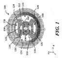
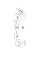
さて、図1を参照するに、本発明の実施形態による電極100の詳細を示す。電極100は、ビームラインイオン注入機のイオンビームを操作するために、用いることができる。特に、イオンビームをターゲットの電位(電圧)に加速するために配置された、複数の電極を有する加速カラムの中で、電極100を用いることができる。電極100は、挿入されたもの102、挿入されたもの102を包囲して配置されたフレーム104、及び、フレーム104を包囲して配置された外側部分106を含むことができる。様々な実施形態により、挿入されたもの102は、フレーム104からリバーシブルに取り付けることができ、フレーム104は、外側部分106からリバーシブルに取り付けることができる。本明細書で用いる用語「リバーシブルに取り付ける」は、コンポーネントが、リバーシブルな方法で、別のコンポーネントから、取り付けられ、及び、取り外されるように、設計されていることを意味する。様々な実施形態において、挿入されたものは第1の導電材料から作ることができ、フレーム104は第2の導電材料から作ることができ、及び、外側部分106は第3の導電材料から作ることができる。様々な実施形態において、挿入されたもの102の第1の導電材料はフレーム104の第2の導電材料と異なることができ、一方、フレーム104の第2の導電材料は、挿入されたもの102の第1の導電材料と異なることができるだけでなく、外側部分106の第3の導電材料とも異なることができる。いくつかの実施形態において、挿入されたもの102、フレーム104、及び、外側部分106の材料は、同じ材料にすることができる。他の実施形態において、挿入されたもの102及びフレーム104などの、コンポーネントの内の2つの材料は同じ材料にすることができ、一方、外側部分106などの第3のコンポーネントの材料は、フレームの材料及び挿入されたものの材料と異なるようにする。実施形態は本文脈に限定されない。様々な実施形態において、フレーム104の材料及び外側部分106の材料だけでなく、挿入されたものの材料102も、ターゲットのアプリケーションにより、変えることができる。電極100は、それに応じて、電極100が、異なるコンポーネントに対して、材料の異なる組合せを含むことができる、モジュール式の構造を提供し、材料は所定のアプリケーションに合うように調整される。
Referring now to FIG. 1, details of an
様々な実施形態において、外側部分106は、電極が単一部分のチタンから成ることができる既知の電極に類似の、チタン又はチタン合金から作ることができる。モジュール式の挿入されたもの及びフレームを、イオンビームを通す所に近い位置に備えることにより、注入プロセス中の汚染を避け、又は、低下させるために、電極100は、挿入されたもの102用の材料を、特に、選択することを可能にする。様々な実施形態において、例えば、挿入されたもの102の材料、及び、フレーム104の材料は、チタン以外の材料から作ることができる。チタンは、電極100により実施される注入プロセスにおける汚染を代表し得るが、これにより、電極100を通るイオンビームによるチタン材料のスパッタリングを防ぐことができる。
In various embodiments, the
さらに図1に示すように、挿入されたもの102は、イオンビームのアパーチャ112を含むことができ、イオンビームを、例えば、図示のデカルト座標のZ軸に沿って、アパーチャに通すようにする。例示的実施形態において、挿入されたもの102は、2.5インチから4インチの外径を備えることができ、一方、イオンビームのアパーチャ112は、1インチから3.2インチの直径を備える。これらの寸法は単に例示であり、実施形態は本文脈に限定されない。
As further shown in FIG. 1, the
例として、異なる実施形態において、挿入されたもの102は、黒鉛、アルミニウム、タングステン、モリブデン、又は、タンタルを含むことができる。実施形態は本文脈に限定されない。高エネルギーイオンにより引き起こされる、特定の材料に衝突するときの放射を避けるだけでなく、チタンから成る従来の電極の使用により引き起こされる、基板の材料汚染を避けるために、これらの材料は、イオン注入という観点から、有用であり得る。例えば、陽子ビームを生成するために電極100を用いる実施形態において、陽子は、MeVの範囲のエネルギーで特定の材料に衝突するときに、ガンマ線放射を生成する傾向があり得る。例として、チタンの約5%の同位体として天然に存在する49Tiは、1.5MeVより大きい陽子エネルギーで衝突するときに、中性子を創生する。別の例として、70keVより大きい高エネルギー陽子により衝突された12Cは、ガンマ線放射を創生し、ガンマ線放射の生成のピークは、420keV及び5MeVで生じる。望ましくない放射の生成をさけるために、生成すべきイオンエネルギーに従って、イオン注入アプリケーションにより、挿入されたものの組成を選択することができることを、当業者は、正しく評価することができる。
By way of example, in different embodiments, insert 102 can include graphite, aluminum, tungsten, molybdenum, or tantalum. Embodiments are not limited to this context. These materials are ion-implanted to avoid radiation when striking certain materials caused by high-energy ions, as well as to avoid material contamination of the substrate caused by the use of conventional electrodes made of titanium. From this point of view, it can be useful. For example, in
上述のとおり、様々な実施形態において、フレーム104は、挿入されたもの102の材料と異なる材料を含むことができる。例えば、挿入されたもの102の材料は、基板の材料汚染を制限するように選択することができ、さらに、ガンマ線などの高エネルギー電磁放射の生成を制限するように設計することができ、一方、フレーム104の材料は、他の考慮すべき事柄により選択することができる。既知のイオン注入機に従って、イオンビームアパーチャ112は、イオンビームアパーチャ112を通るイオンビームの呼び直径が、イオンビームアパーチャ112の直径より小さいように、イオンビームを入れるサイズにすることができる。したがって、イオンビームがイオンビームアパーチャ112内の中心にあるとき、イオンビームにより不注意でスパッタされる電極100からのほとんどの材料は、挿入されたもの102がイオンビームに最も近くに配置されるため、通常、挿入されたもの102からの材料であり得る。一例において、例示の目的のため、挿入されたもの102の外径は4インチにすることができ、一方、イオンビームアパーチャ112の最大内径は2.5インチにすることができる。イオンビームアパーチャ112を通過するイオンビームの呼び直径が2.5インチより小さいという仮定の下で、フレーム104の内径はイオンビームアパーチャ112の外径(4インチ)と同じため、イオンビームは、フレーム104からのどの材料にも突き当る可能性が低くなり得る。したがって、フレーム104は、イオンビームからのスパッタリングによる汚染が最優先の検討課題ではない一群の材料から選択することができる。例えば、いくつかの実施形態において、フレーム104は、高熱伝導材料を含むことができる。高熱伝導材料は、50W/m-K以上の熱伝導率を有することができる。例えば、アルミニウムをフレーム104として用いることができ、アルミニウムは、熱伝導率が20W/m-Kの範囲の中にあるチタンとは対照的に、約200W/m-Kの(室温)熱伝導率を有することができる。他の実施形態において、アルミニウムとは異なる他の材料を、フレーム104用の材料として、選択することができる。フレーム104用に高い熱伝導材料を提供することにより、特に、熱伝導率が熱輸送において大きな役割を演じる温度範囲を、加速器カラムが生成する状況において、加速器カラムの1つの又は一連の電極で発生する熱を、もっと効率的に放散することができる。いくつかの実施形態において、挿入されたもの102用の材料は、フレーム104用の材料と同様に、放射により熱を放散するための、挿入されたもの102又はフレーム104の機能により、選択することができる。例えば、加速器カラムは、電極コンポーネントの温度が最大で2800Kまで達し得る条件下で動作することができる。そのような高温下で、主要な熱輸送は放射により行うことができる。例として、黒鉛は、2800Kにおいて35W/cm2の速度で熱を放射することができ、電極から熱を放散するために都合の良い、挿入されたものの材料及びフレームの材料を提供し、挿入されたものは、高真空の中にあり、電極の他の部分とわずかな小領域の接触を有し、接触の小領域は熱伝導が起こり得る位置を提供する、条件下で、特に重要な材料である。
As noted above, in various embodiments, the
様々な追加の実施形態において、挿入されたもの又はフレーム用の材料の選択は、追加の考慮すべき事柄により導くことができる。黒鉛は、通常、機械加工性が良く、半導体材料の低汚染のため、多くの応用に有用であり得るが、例えば、非常に薄い板状であり、圧入によるアセンブリなどの変形に依存するプロセスにおいて、黒鉛を成形するために、制限がある。アルミニウムは、低コスト、低重量及び加工容易性のため、有用であり得る。アルミニウムの使用の制限は、基板の汚染を避けることを含み、シリコンの黒鉛によるアルミニウムのコーティングは、この問題に対処することができる。第2に、アルミニウム及びその合金は、また、約300℃以下の低い最大加工温度を有する。タンタル又はタングステンは、腐食抵抗を必要とする高温アプリケーション用の挿入されたもの又はフレームの材料として、用いることができる。タングステン及びタンタルの短所は、それらの高重量及び低い加工性である。したがって、挿入されたもの及びフレームの材料の選択は、上記のように、考慮すべき事柄のバランスに基づいて実施することができる。 In various additional embodiments, the selection of materials for the insert or frame may be guided by additional considerations. Graphite can be useful in many applications due to its generally good machinability and low contamination of semiconductor materials, for example, in processes that rely on deformation, such as very thin platelets and assembly by press-fitting. , to shape graphite, there are limitations. Aluminum can be useful because of its low cost, low weight and ease of processing. Limitations on the use of aluminum include avoiding contamination of the substrate, and coating aluminum with silicon graphite can address this issue. Second, aluminum and its alloys also have low maximum working temperatures of about 300° C. or less. Tantalum or tungsten can be used as the insert or frame material for high temperature applications requiring corrosion resistance. A disadvantage of tungsten and tantalum is their high weight and poor workability. Therefore, the selection of insert and frame material can be made based on a balance of considerations, as described above.
さらに図1に示すように、挿入されたもの102は、挿入されたもの102とフレーム104との間に内側アパーチャ116を画定するように、設計することができる。フレーム104は、さらに、図示のフレームアパーチャ118を含むことができ、さらに、外側部分106と共に、外側アパーチャ114を画定するように、設計することができる。通常、既知のイオン注入機におけるように、例えば、ガスを電極及び加速器カラムに通すために、これらのアパーチャを用いることができる。
Further, as shown in FIG. 1, insert 102 can be designed to define an
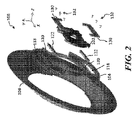
さて、図2を見るに、電極100の実施形態が示され、電極100は、この場合、図示の2つの部分に配置されたカバー部分130を含む。組み立てられたときのカバー部分130は、挿入されたもの102をフレーム104に取り付けるように、少なくとも部分的に挿入されたもの102の上に配置することができる。カバー部分130は、ねじなどのリバーシブルファスナー132を用いて、フレーム104に取り付けることができる。このように、カバー部分130は、また、挿入されたもの102をフレーム104に対して適切な位置で支えることができる。他の既知の留め付け機構は、挿入されたもの102をフレーム104に、リバーシブルな取り外し可能な方法で、取り付けるために、用いることができるので、本実施形態は本文脈に限定されない。したがって、有用であるときは、挿入されたもの102は、フレーム104から分離して取り除くことができ、クリーニングのため、又は、挿入されたもの102用の異なる材料、もしくは、材料は同じである挿入されたものの代わりなどの電極100において異なる挿入されたものを用いるべきときなどのためである。
Turning now to FIG. 2, an embodiment of
図2にさらに示すように、フレーム104は、本例において、フレーム104の2つの異なる領域において配置される凹部分120を含むことができる。凹部分120は、磁石アセンブリ122を収容するように配置することができ、磁石アセンブリ122は図示の2つの磁石を含むことができる。これらの磁石は、既知の加速器カラムの電極におけるように、荷電粒子を制御するために用いることができる。本文脈において、カバー部分130は、非磁性材料にすることができ、また、凹部分120において、磁石アセンブリ122を適切な位置で支えることができる。
As further shown in FIG. 2, the
図1にさらに示すように、外側部分106は連結部分124を含むことができ、連結部分124は、図示のように、フレーム104の外側領域に係合するように設計される。連結部分124は、フレーム104を外側部分106からリバーシブルに取り付けかつ取り外せるように配置された、タブ、凹部又は類似の機構、又は機構の組合せにすることができる。いくつかの例において、フレーム104は、既知の設計におけるように、外側部分106に回転自在に取り付け可能にすることができる。したがって、有用であるときは、フレーム104は、外側部分106から分離して取り除くことができ、クリーニングのため、又は、フレーム104用の異なる材料、もしくは、材料は同じであるフレーム104用の代わりなどの電極100において異なるフレームを用いるべきとき、又は、外側部分106用の異なるコンポーネントを用いるべきとき、などのためである。
As further shown in FIG. 1,
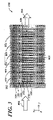
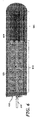
さて、図3を見るに、本発明の実施形態による、加速器カラム300が示される。加速器カラム300は、通常、上記のように電極100として示される複数の電極を含む電極アセンブリを含むことができる。加速器カラム300は、絶縁体302を含むことができ、絶縁体302は隣接する電極の間に配置され、したがって、電極100は、既知の加速器カラムにおけるように、互いに電気的に絶縁される。加速器カラム300は、図示のように、加速器カラム300にイオンビーム304を通すように配置することができ、電極100の異なる電極は、加速器カラム300を通って伸びるカラムアパーチャ306を画定する。イオンビーム304用のターゲットイオンエネルギーを得るために、異なる電極間で(絶対的大きさにおいて)単調に増加する電圧などの異なる電圧を、異なる電極に印加することができる。例として、加速器カラム300が25個の電極を含む場合、40kVの電圧を、加速器カラム300の左の第1の入り口の電極に印加することができ、一方、増加する電圧を、第1の電極の右に続く電極に印加することができる。いくつかの実施形態において、隣接する電極間の40kVの増加などのように、電圧を連続する電極間に均一に増加することができ、25個の電極のアセンブリは1MeVの電圧の変化を生成する。本実施形態は本文脈に限定されない。本発明の様々な実施形態により、電極100として示す、少なくとも1つの電極は、図1及び図2に示すように、挿入されたもの102を含むように、配置することができ、挿入されたもの102は、上記のように、材料又は放射の汚染を低減するために選択された材料から、作ることができる。加速器カラム300は、既知の加速器カラムと同じ一般のサイズ及び形状を有するように、配置することができ、したがって、本実施形態の新規な電極は、既知のイオン注入機の構成内に適合することができる。
Turning now to Figure 3, an
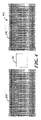
いくつかの実施形態において、加速器カラム300などの加速器カラムは、2つの異なる加速器カラムを含むタンデム加速器の中に配置することができる。さて、図4を見るに、本発明の実施形態による、タンデム加速器400の側面図が示される。図4に示すように、タンデム加速器400は、第1の加速器カラム402、第1の加速器カラム402に隣接して配置された電荷交換チャンバ404、及び、電荷交換チャンバ404に隣接して配置され、かつ、第1の加速器カラム402の下流に配置された第2の加速器カラム406を含む。
In some embodiments, an accelerator column such as
既知のタンデム加速器におけるように、タンデム加速器400は、イオンビームのイオンを30keVより大きいエネルギーなどの高エネルギーへ加速するために、使用することができる。本実施形態は本文脈に限定されない。タンデム加速器において、第1のイオン種は、第1の加速器カラムにおいて、ターゲットエネルギーに加速することができ、続いて電荷交換プロセスがあり、イオン種は、例えば、正のイオンから負のイオンへ変わることができる。別の例において、第1のイオン種は、電荷交換プロセスにおいて、正のイオンに変えられるべき負のイオンであり得る。新しいイオン種は、さらにイオンエネルギーを増大するために、第2の加速器カラムにより加速することができる。既知のタンデム加速器におけるように、新しいイオン種の電荷は第1のイオン種の電荷と反対であり得るため、第2の加速器カラムは、第1の加速器カラムと比べて、シーケンスにおいて逆の、個々の電極に印加される、電圧を有することができる。例えば、第1の加速器カラムは、一価の負のイオンを1MeVのイオンエネルギーへ加速することができ、一方、第2の加速器カラムは、1MeVの最初のエネルギーを有する一価の正のイオンを2MeVのエネルギーへ加速する。電荷交換チャンバに隣接する、第1の加速器カラム及び第2の加速器カラムの中の、電極において、最大の電圧が存在し得る。
As in known tandem accelerators,
いくつかの実施形態において、タンデム加速器400の第1の加速器カラム402は、複数の電極を用いて構成することができ、異なる電極のほとんど又は全ては、上記の電極100の構造などの、お互いに同じ構造を有する。同じく第2の加速器カラム406に適用することができ、電極も上記の電極100のように配置することができる。いくつかの実施形態において、加速器カラムは、可変のイオンビームのアパーチャサイズを備えることができ、加速器カラムの第1の電極の第1のイオンビームのアパーチャは第1の直径を有し、加速器カラムの第2の電極の第2のイオンビームのアパーチャは第2の直径を有し、第2の直径は第1の直径と異なる。例えば、円すい形のイオンビームのアパーチャを画定するために、挿入されたもの102のアパーチャサイズが1つの電極から次の電極へ単調に変化するように、一連の電極を配置することができる。
In some embodiments, the
本発明のいくつかの実施形態において、加速器カラムは、第1の電極アセンブリ及び追加の電極アセンブリ又は第2の電極アセンブリを含むことができ、第2の電極アセンブリは、第1の電極アセンブリに隣接して配置され、構造又は材料において、第1の電極アセンブリとは異なる。例えば、加速器カラムの第1の電極アセンブリは、挿入されたもの102、フレーム104及び外側部分106を含む電極100に対して説明したように、通常、構成される複数の電極を含むことができる。特定の変形において、第1の電極アセンブリの複数の電極は、同じイオンビームのアパーチャサイズを有することができ、一方、他の変形において、第1の電極アセンブリの複数の電極は、異なる電極間で変化するイオンビームのアパーチャサイズを画定することができる。本発明の様々な実施形態において、第2の電極アセンブリは、電導材料からの単一構造として構成することができ、第2の電極アセンブリは少なくとも1つの追加の電極を含む。第2の電極アセンブリは、例えば、既知の構造を有する複数のチタンの電極から構成することができる。単一構造により、電極は、通常、1つの部分を構成するが、たとえ、もともと、1つの部分より多いものから形成されたとしても、その1つの部分は、通常、分解されず、分解することができない。単一構造は、さらに、単一の材料から形成することができる。例えば、既知のチタンの電極は、チタンだけから形成することができ、通常、分解することができない。2つの異なる電極アセンブリを有する加速器カラムを提供することにより、加速器カラムは、加速器カラムのターゲット部分において、本実施形態により配置された電極を含むことができ、一方、加速器カラムの他の部分において、既知の構造の電極を含むことができる。この2つのアセンブリの構成は、コストの考慮、メンテナンス、組み立ての容易さ、同心性、及び、他の考慮すべき事柄において、支援するために有用であり得る。
In some embodiments of the invention, the accelerator column can include a first electrode assembly and an additional electrode assembly or a second electrode assembly, the second electrode assembly adjacent to the first electrode assembly. and is different in structure or material from the first electrode assembly. For example, the first electrode assembly of the accelerator column may include multiple electrodes generally configured as described for
さて、図6を見るに、本発明のさらなる実施形態による、加速器カラム600の側面図が示される。本実施形態において、加速器カラム600は、第1の電極アセンブリ602、及び、第1の電極アセンブリ602に隣接して配置された第2の電極アセンブリ604を含む。加速器カラム600は、いくつかの実施形態において、タンデム加速器の部分を形成することができる。特定の実施形態において、加速器カラム600は、タンデム加速器において、下流の加速器カラムを形成することができ、イオンビーム304は、電荷交換プロセスの後に、図示のように、右から入る。様々な実施形態において、第1の電極アセンブリは、電極100と同じ通常の構造を有する電極を含むことができ、一方、イオンビームのアパーチャサイズは、既知の加速器カラムにおけるように、イオンビームのアパーチャ606として示される、可変サイズのイオンビームのアパーチャを画定するように、電極間で変わり得る。本例において、イオンビームのアパーチャ606のアパーチャサイズは、第1の電極アセンブリ602内で左から右へ増加することができる。第2の電極アセンブリ604は、いくつかの例におけるチタンの電極などの、既知の電極を用いて形成することができる。図6により示唆されるように、第2の電極アセンブリ604のイオンビームのアパーチャ608のイオンビームのアパーチャサイズは、一定にすることができる。
Turning now to Figure 6, a side view of an
いくつかの実施形態において、ミラー・イメージではあるが、同様に構成された加速器カラムは、タンデム加速器において、上流の加速器カラムを形成することができる。追加の実施形態において、タンデム加速器の上流の加速器カラムは、加速器カラム600と異なって構成することができる。
In some embodiments, a mirror image but similarly configured accelerator column can form the upstream accelerator column in a tandem accelerator. In additional embodiments, the accelerator column upstream of the tandem accelerator can be configured differently than
加速器カラムの再設計をせずに、中エネルギー及び高エネルギーのイオン注入機の汚染を防ぐ機能を含む、本実施形態により提供される、多数の優位性がある。さらに、本実施形態は、適切なときに、中心部分(挿入されたもの)のみを選択的に交換することができる、単一電極設計を提供することにより、イオン注入処理において、フレキシビリティーを提供する。 There are a number of advantages provided by this embodiment, including the ability to prevent contamination of medium and high energy ion implanters without redesigning the accelerator column. Further, the present embodiment provides flexibility in ion implantation processes by providing a single electrode design that allows selective replacement of only the central portion (inserted) when appropriate. offer.
本発明は、本明細書に記載された特定の実施形態によって範囲を限定されるものではない。実際に、本明細書に記載された実施形態に加えて、本発明の他の様々な実施形態および変更は、前述の記載および添付図面から当業者には明らかであろう。したがって、このような他の実施形態および変更は、本発明の範囲内に含まれるものと意図している。さらに、本発明は、特定の環境における特定の目的のための特定の実装の文脈にて本明細書中で説明したけれども、当業者は、その有用性はそれらに限定されるものでなく、本発明は任意の数の環境における任意の数の目的のために有益に実装し得ることを認識するであろう。従って、以下に記載する特許請求の範囲は本明細書に記載された本発明の全範囲及び精神に鑑みて解釈しなければならない。
The invention is not to be limited in scope by the specific embodiments described herein. Indeed, various other embodiments and modifications of the invention, in addition to those described herein, will become apparent to those skilled in the art from the foregoing description and accompanying drawings. Accordingly, such other embodiments and modifications are intended to be included within the scope of this invention. Furthermore, although the present invention has been described herein in the context of particular implementations for particular purposes in particular environments, those skilled in the art will appreciate that its utility is not limited thereto and that the present invention It will be appreciated that the invention may be beneficially implemented for any number of purposes in any number of environments. Therefore, the following claims should be interpreted in light of the full scope and spirit of the invention described herein.
Claims (9)
イオンビームを通すようにする、該イオンビームのアパーチャを有する、挿入されたものであって、前記電極の中心部分に配置され、第1の導電材料を備える、挿入されたものと、
該挿入されたものを包囲して配置され、第2の導電材料を備える、フレームと、
該フレームを包囲して配置され、第3の導電材料を備える、外側部分と、を備え、
前記挿入されたものは、前記フレームからリバーシブルに取り付けることができ、前記フレームは、前記外側部分からリバーシブルに取り外すことができ、
前記第1の導電材料は前記第2の導電材料と異なり、前記第2の導電材料は前記第3の導電材料と異なり、
前記挿入されたものは、黒鉛又はタンタルを含み、
前記フレームは、高熱伝導材料を含み、
前記外側部分は、チタンを含み、前記挿入されたものは、チタンを含まない、電極。 An electrode for manipulating an ion beam, the electrode comprising:
an insert having an ion beam aperture adapted to pass the ion beam, the insert being disposed in a central portion of the electrode and comprising a first conductive material;
a frame disposed surrounding the insert and comprising a second conductive material;
an outer portion disposed surrounding the frame and comprising a third conductive material;
the insert can be reversibly attached to the frame and the frame can be reversibly removed from the outer portion;
the first conductive material is different from the second conductive material, the second conductive material is different from the third conductive material, and
the insert comprises graphite or tantalum;
the frame comprises a highly thermally conductive material;
The electrode, wherein the outer portion comprises titanium and the insert is free of titanium .
第1の複数の電極を備える電極アセンブリを備え、該第1の複数の電極は、互いに電気的に絶縁され、
前記電極アセンブリの所定の電極は、
前記イオンビームを通すようにする、前記イオンビームのアパーチャを有し、前記電極の中心部分に配置される、挿入されたものと、
該挿入されたものを包囲して配置される、フレームと、
該フレームを包囲して配置される、外側部分と、を備え、
前記挿入されたものを前記フレームからリバーシブルに取り付けることができ、前記フレームを前記外側部分からリバーシブルに取り外すことができ、前記挿入されたもの、前記フレーム及び前記外側部分は導電性であり、
前記挿入されたものは第1の材料を備え、前記フレームは第2の材料を備え、前記外側部分は第3の材料を備え、
前記第1の材料は前記第2の材料と異なり、前記第2の材料は前記第3の材料と異なり、
前記挿入されたものは、黒鉛又はタンタルを含み、
前記フレームは、高熱伝導材料を含み、
前記外側部分は、チタンを含み、前記挿入されたものは、チタンを含まない、加速器カラム。 An accelerator column for accelerating an ion beam, the accelerator column comprising:
an electrode assembly comprising a first plurality of electrodes, the first plurality of electrodes electrically isolated from each other;
A given electrode of the electrode assembly comprises:
an insert positioned at a central portion of the electrode and having an aperture for the ion beam to allow the ion beam to pass through;
a frame disposed surrounding the insert;
an outer portion disposed surrounding the frame;
said insert is reversibly attachable from said frame, said frame is reversibly removable from said outer portion, said insert, said frame and said outer portion are electrically conductive;
said insert comprising a first material, said frame comprising a second material and said outer portion comprising a third material;
said first material is different from said second material, said second material is different from said third material,
the insert comprises graphite or tantalum;
the frame comprises a highly thermally conductive material;
The accelerator column , wherein the outer portion comprises titanium and the insert is free of titanium .
イオンビームを生成するためのイオン源と、
前記イオンビームを加速するための加速器カラムであって、前記イオン源の下流に配置される加速器カラムと、を備え、
該加速器カラムは、第1の加速器カラムを備え、
該第1の加速器カラムは、
第1の複数の電極を備える第1の電極アセンブリを備え、該第1の複数の電極は、互いに電気的に絶縁され、
前記第1の電極アセンブリの所定の電極は、
前記イオンビームを通すようにする、前記イオンビームのアパーチャを有し、前記電極の中心部分に配置される、挿入されたものと、
該挿入されたものを包囲して配置される、フレームと、
該フレームを包囲して配置される、外側部分と、を備え、
前記挿入されたものを前記フレームからリバーシブルに取り外すことができ、前記フレームを前記外側部分からリバーシブルに取り付けることができ、前記挿入されたもの、前記フレーム及び前記外側部分は導電性であり、
前記第1の加速器カラムは,さらに,第2の電極アセンブリを備え、該第2の電極アセンブリは前記第1の電極アセンブリに隣接して配置され、前記第2の電極アセンブリは少なくとも1つの追加の電極を備え、該少なくとも1つの追加の電極は単一構造を有する電導材料を備え、
前記挿入されたものは、黒鉛又はタンタルを含み、
前記フレームは、高熱伝導材料を含み、
前記外側部分は、チタンを含み、前記挿入されたものは、チタンを含まない、イオン注入機。 An ion implanter, the ion implanter comprising:
an ion source for generating an ion beam;
an accelerator column for accelerating the ion beam, the accelerator column positioned downstream of the ion source;
The accelerator column comprises a first accelerator column;
The first accelerator column comprises:
a first electrode assembly comprising a first plurality of electrodes, the first plurality of electrodes electrically isolated from each other;
A predetermined electrode of the first electrode assembly comprises:
an insert positioned at a central portion of the electrode and having an aperture for the ion beam to allow the ion beam to pass through;
a frame disposed surrounding the insert;
an outer portion disposed surrounding the frame;
said insert is reversibly removable from said frame, said frame is reversibly attachable from said outer portion, said insert, said frame and said outer portion are electrically conductive;
The first accelerator column further comprises a second electrode assembly, the second electrode assembly positioned adjacent to the first electrode assembly, the second electrode assembly including at least one additional an electrode, the at least one additional electrode comprising a conductive material having a unitary structure ;
the insert comprises graphite or tantalum;
the frame comprises a highly thermally conductive material;
The ion implanter , wherein the outer portion comprises titanium and the insert is titanium free .
前記第1の加速器カラムに隣接して配置される電荷交換チャンバと、
該電荷交換チャンバに隣接して、前記第1の加速器カラムの下流に配置される第2の加速器カラムと、を備え、該第2の加速器カラムは、
第2の複数の電極を備える追加の電極アセンブリを備え、該第2の複数の電極は、互いに電気的に絶縁され、
前記追加の電極アセンブリの所定の電極は、
イオンビームを通すようにする、前記イオンビームのアパーチャを有する、挿入されたものと、
該挿入されたものを包囲して配置される、フレームと、
該フレームを包囲して配置される、外側部分と、を備え、
前記挿入されたものを前記フレームからリバーシブルに取り外すことができ、前記フレームを前記外側部分からリバーシブルに取り付けることができ、前記挿入されたもの、前記フレーム及び前記外側部分は導電性である、請求項8記載のイオン注入機。 The ion implanter further comprises:
a charge exchange chamber positioned adjacent to the first accelerator column;
a second accelerator column positioned adjacent to the charge exchange chamber and downstream of the first accelerator column, the second accelerator column comprising:
an additional electrode assembly comprising a second plurality of electrodes, the second plurality of electrodes electrically isolated from each other;
A predetermined electrode of the additional electrode assembly comprises:
an inserted having an ion beam aperture adapted to pass the ion beam;
a frame disposed surrounding the insert;
an outer portion disposed surrounding the frame;
4. The insert is reversibly removable from the frame, the frame is reversibly attachable from the outer portion, and wherein the insert, the frame and the outer portion are electrically conductive. 9. The ion implanter according to 8 .
Applications Claiming Priority (3)
| Application Number | Priority Date | Filing Date | Title |
|---|---|---|---|
| US15/228,158 | 2016-08-04 | ||
| US15/228,158 US9807864B1 (en) | 2016-08-04 | 2016-08-04 | Electrode, accelerator column and ion implantation apparatus including same |
| PCT/US2017/043277 WO2018026543A1 (en) | 2016-08-04 | 2017-07-21 | Electrode, accelerator column and ion implantation apparatus including same |
Publications (3)
| Publication Number | Publication Date |
|---|---|
| JP2019523531A JP2019523531A (en) | 2019-08-22 |
| JP2019523531A5 JP2019523531A5 (en) | 2020-05-28 |
| JP7194100B2 true JP7194100B2 (en) | 2022-12-21 |
Family
ID=60142632
Family Applications (1)
| Application Number | Title | Priority Date | Filing Date |
|---|---|---|---|
| JP2019503740A Active JP7194100B2 (en) | 2016-08-04 | 2017-07-21 | Electrodes, accelerator columns and ion implanters containing them |
Country Status (6)
| Country | Link |
|---|---|
| US (1) | US9807864B1 (en) |
| JP (1) | JP7194100B2 (en) |
| KR (1) | KR102448490B1 (en) |
| CN (1) | CN109478487B (en) |
| TW (1) | TWI749021B (en) |
| WO (1) | WO2018026543A1 (en) |
Families Citing this family (1)
| Publication number | Priority date | Publication date | Assignee | Title |
|---|---|---|---|---|
| KR20210003770A (en) | 2018-04-30 | 2021-01-12 | 뉴트론 쎄라퓨틱스 인코포레이티드 | Small motor driven insulated electrostatic particle accelerator |
Citations (3)
| Publication number | Priority date | Publication date | Assignee | Title |
|---|---|---|---|---|
| JP2003178688A (en) | 2001-12-12 | 2003-06-27 | Shin Etsu Handotai Co Ltd | Extraction electrode system of ion implanter and ion implanter |
| US20160064186A1 (en) | 2014-08-26 | 2016-03-03 | Varian Semiconductor Equipment Associates, Inc. | Bias electrodes for tandem accelerator |
| CN205726638U (en) | 2016-06-07 | 2016-11-23 | 中国工程物理研究院核物理与化学研究所 | A kind of high current quadrupole lens ion accelerating tube |
Family Cites Families (13)
| Publication number | Priority date | Publication date | Assignee | Title |
|---|---|---|---|---|
| US3328618A (en) | 1965-09-13 | 1967-06-27 | High Voltage Engineering Corp | High-voltage acceleration tube with inserts for the electrodes |
| US5095208A (en) * | 1988-06-24 | 1992-03-10 | Hitachi, Ltd. | Charged particle generating device and focusing lens therefor |
| JPH03102800A (en) * | 1989-09-18 | 1991-04-30 | Shimadzu Corp | High frequency multi-pole wire type accelerator |
| JPH04294043A (en) * | 1991-03-22 | 1992-10-19 | Matsushita Electron Corp | Charge-up control device for ion implanting machine |
| JPH088097A (en) * | 1994-06-20 | 1996-01-12 | Nissin High Voltage Co Ltd | Electrostatic ion accelerator |
| JPH10270196A (en) * | 1997-03-25 | 1998-10-09 | Nissin High Voltage Co Ltd | Accelerating tube for ion accelerator |
| US20060043316A1 (en) * | 2003-06-10 | 2006-03-02 | Varian Semiconductor Equipment Associates, Inc. | Ion implanter having enhanced low energy ion beam transport |
| KR100538813B1 (en) * | 2004-07-31 | 2005-12-23 | 주식회사 하이닉스반도체 | Implanter for uniformity of transistor parameter and method for implantation using the same |
| US20070221862A1 (en) * | 2006-03-22 | 2007-09-27 | Wayne State University | Coupled Electrostatic Ion and Electron Traps for Electron Capture Dissociation - Tandem Mass Spectrometry |
| GB0703044D0 (en) * | 2007-02-16 | 2007-03-28 | Nordiko Technical Services Ltd | Apparatus |
| CN101296555A (en) * | 2007-04-25 | 2008-10-29 | 和舰科技(苏州)有限公司 | Ion accelerator |
| US9053895B2 (en) * | 2011-11-30 | 2015-06-09 | Fei Company | System for attachment of an electrode into a plasma source |
| WO2015071439A1 (en) * | 2013-11-14 | 2015-05-21 | Mapper Lithography Ip B.V. | Multi-electrode stack arrangement |
-
2016
- 2016-08-04 US US15/228,158 patent/US9807864B1/en active Active
-
2017
- 2017-06-23 TW TW106121013A patent/TWI749021B/en active
- 2017-07-21 WO PCT/US2017/043277 patent/WO2018026543A1/en active Application Filing
- 2017-07-21 CN CN201780045501.3A patent/CN109478487B/en active Active
- 2017-07-21 JP JP2019503740A patent/JP7194100B2/en active Active
- 2017-07-21 KR KR1020197005409A patent/KR102448490B1/en active IP Right Grant
Patent Citations (3)
| Publication number | Priority date | Publication date | Assignee | Title |
|---|---|---|---|---|
| JP2003178688A (en) | 2001-12-12 | 2003-06-27 | Shin Etsu Handotai Co Ltd | Extraction electrode system of ion implanter and ion implanter |
| US20160064186A1 (en) | 2014-08-26 | 2016-03-03 | Varian Semiconductor Equipment Associates, Inc. | Bias electrodes for tandem accelerator |
| CN205726638U (en) | 2016-06-07 | 2016-11-23 | 中国工程物理研究院核物理与化学研究所 | A kind of high current quadrupole lens ion accelerating tube |
Also Published As
| Publication number | Publication date |
|---|---|
| CN109478487A (en) | 2019-03-15 |
| WO2018026543A1 (en) | 2018-02-08 |
| TW201816828A (en) | 2018-05-01 |
| KR20190026938A (en) | 2019-03-13 |
| KR102448490B1 (en) | 2022-09-28 |
| US9807864B1 (en) | 2017-10-31 |
| JP2019523531A (en) | 2019-08-22 |
| CN109478487B (en) | 2021-02-19 |
| TWI749021B (en) | 2021-12-11 |
Similar Documents
| Publication | Publication Date | Title |
|---|---|---|
| US9711318B2 (en) | Ribbon beam ion source of arbitrary length | |
| US9214313B2 (en) | Ion source with independent power supplies | |
| US8508134B2 (en) | Hall-current ion source with improved ion beam energy distribution | |
| US5757018A (en) | Zero deflection magnetically-suppressed Faraday for ion implanters | |
| CN1477984A (en) | Ion implantation system and control method | |
| JP6186541B1 (en) | Tandem accelerator and ion implantation system | |
| WO2008147846A1 (en) | Method and system for extracting ion beams composed of molecular ions (cluster ion beam extraction system) | |
| Lencová | Electrostatic lenses | |
| TW201214500A (en) | Deceleration lens | |
| JP2010519681A (en) | Ion beam accelerator with electrodes mounted on a movable mount | |
| JP7194100B2 (en) | Electrodes, accelerator columns and ion implanters containing them | |
| Arredondo et al. | SIESTA: a high current ion source for erosion and retention studies | |
| JPH05190129A (en) | Electrostatic type lens | |
| JP2012523092A (en) | Termination for electrodes used in ion implantation systems | |
| US9818575B2 (en) | Low profile extraction electrode assembly | |
| US11031205B1 (en) | Device for generating negative ions by impinging positive ions on a target | |
| Weisser et al. | Novel matching lens and spherical ionizer for a cesium sputter ion source | |
| White | DC Parallel Ribbon Ion Beams for High-Dose Processes | |
| US20220359157A1 (en) | System and process implementing a wide ribbon beam ion source to implant ions in material to modify material properties | |
| Yahya et al. | Effects of External Magnetic Field on Focusing and Energy Distribution of Primary Electrons in an Ion Source | |
| Barth et al. | Gas ion source for focused beams | |
| Inami et al. | Development of a high current and high energy metal ion beam system | |
| Pinsley | Characteristics of a Surface Contact Hall Current Accelerator | |
| WO2012173989A2 (en) | Array structures for field-assisted positron moderation and corresponding methods | |
| Renau et al. | The VIISion 80 and VIISion 200 ion implanter beam lines |
Legal Events
| Date | Code | Title | Description |
|---|---|---|---|
| A521 | Request for written amendment filed |
Free format text: JAPANESE INTERMEDIATE CODE: A523 Effective date: 20200416 |
|
| A621 | Written request for application examination |
Free format text: JAPANESE INTERMEDIATE CODE: A621 Effective date: 20200416 |
|
| A131 | Notification of reasons for refusal |
Free format text: JAPANESE INTERMEDIATE CODE: A131 Effective date: 20210316 |
|
| A521 | Request for written amendment filed |
Free format text: JAPANESE INTERMEDIATE CODE: A523 Effective date: 20210608 |
|
| A131 | Notification of reasons for refusal |
Free format text: JAPANESE INTERMEDIATE CODE: A131 Effective date: 20210914 |
|
| A521 | Request for written amendment filed |
Free format text: JAPANESE INTERMEDIATE CODE: A523 Effective date: 20211210 |
|
| A131 | Notification of reasons for refusal |
Free format text: JAPANESE INTERMEDIATE CODE: A131 Effective date: 20220308 |
|
| A521 | Request for written amendment filed |
Free format text: JAPANESE INTERMEDIATE CODE: A523 Effective date: 20220602 |
|
| A02 | Decision of refusal |
Free format text: JAPANESE INTERMEDIATE CODE: A02 Effective date: 20220809 |
|
| A521 | Request for written amendment filed |
Free format text: JAPANESE INTERMEDIATE CODE: A523 Effective date: 20220922 |
|
| C60 | Trial request (containing other claim documents, opposition documents) |
Free format text: JAPANESE INTERMEDIATE CODE: C60 Effective date: 20220922 |
|
| A911 | Transfer to examiner for re-examination before appeal (zenchi) |
Free format text: JAPANESE INTERMEDIATE CODE: A911 Effective date: 20221005 |
|
| C21 | Notice of transfer of a case for reconsideration by examiners before appeal proceedings |
Free format text: JAPANESE INTERMEDIATE CODE: C21 Effective date: 20221011 |
|
| TRDD | Decision of grant or rejection written | ||
| A01 | Written decision to grant a patent or to grant a registration (utility model) |
Free format text: JAPANESE INTERMEDIATE CODE: A01 Effective date: 20221115 |
|
| A61 | First payment of annual fees (during grant procedure) |
Free format text: JAPANESE INTERMEDIATE CODE: A61 Effective date: 20221209 |
|
| R150 | Certificate of patent or registration of utility model |
Ref document number: 7194100 Country of ref document: JP Free format text: JAPANESE INTERMEDIATE CODE: R150 |