JP7181653B2 - plasma actuator - Google Patents
plasma actuator Download PDFInfo
- Publication number
- JP7181653B2 JP7181653B2 JP2021542840A JP2021542840A JP7181653B2 JP 7181653 B2 JP7181653 B2 JP 7181653B2 JP 2021542840 A JP2021542840 A JP 2021542840A JP 2021542840 A JP2021542840 A JP 2021542840A JP 7181653 B2 JP7181653 B2 JP 7181653B2
- Authority
- JP
- Japan
- Prior art keywords
- electrode
- conductor
- dielectric layer
- plasma actuator
- covered
- Prior art date
- Legal status (The legal status is an assumption and is not a legal conclusion. Google has not performed a legal analysis and makes no representation as to the accuracy of the status listed.)
- Active
Links
- 239000004020 conductor Substances 0.000 claims description 370
- 230000004888 barrier function Effects 0.000 claims description 12
- 239000003989 dielectric material Substances 0.000 claims description 10
- 239000010410 layer Substances 0.000 description 121
- 238000010586 diagram Methods 0.000 description 12
- 230000004048 modification Effects 0.000 description 12
- 238000012986 modification Methods 0.000 description 12
- 238000002474 experimental method Methods 0.000 description 9
- 238000007789 sealing Methods 0.000 description 9
- 230000000052 comparative effect Effects 0.000 description 8
- 229920002050 silicone resin Polymers 0.000 description 7
- 239000012530 fluid Substances 0.000 description 6
- 230000005684 electric field Effects 0.000 description 5
- 238000010292 electrical insulation Methods 0.000 description 5
- RYGMFSIKBFXOCR-UHFFFAOYSA-N Copper Chemical compound [Cu] RYGMFSIKBFXOCR-UHFFFAOYSA-N 0.000 description 4
- 230000000694 effects Effects 0.000 description 4
- 239000002245 particle Substances 0.000 description 4
- 229920001343 polytetrafluoroethylene Polymers 0.000 description 4
- 239000004810 polytetrafluoroethylene Substances 0.000 description 4
- 229920005989 resin Polymers 0.000 description 4
- 239000011347 resin Substances 0.000 description 4
- 239000004809 Teflon Substances 0.000 description 3
- 229920006362 Teflon® Polymers 0.000 description 3
- 239000012212 insulator Substances 0.000 description 3
- -1 polytetrafluoroethylene Polymers 0.000 description 3
- PXHVJJICTQNCMI-UHFFFAOYSA-N Nickel Chemical compound [Ni] PXHVJJICTQNCMI-UHFFFAOYSA-N 0.000 description 2
- 239000004642 Polyimide Substances 0.000 description 2
- BQCADISMDOOEFD-UHFFFAOYSA-N Silver Chemical compound [Ag] BQCADISMDOOEFD-UHFFFAOYSA-N 0.000 description 2
- PNEYBMLMFCGWSK-UHFFFAOYSA-N aluminium oxide Inorganic materials [O-2].[O-2].[O-2].[Al+3].[Al+3] PNEYBMLMFCGWSK-UHFFFAOYSA-N 0.000 description 2
- 239000000919 ceramic Substances 0.000 description 2
- 239000011248 coating agent Substances 0.000 description 2
- 238000000576 coating method Methods 0.000 description 2
- 229910052802 copper Inorganic materials 0.000 description 2
- 239000010949 copper Substances 0.000 description 2
- 239000011889 copper foil Substances 0.000 description 2
- PCHJSUWPFVWCPO-UHFFFAOYSA-N gold Chemical compound [Au] PCHJSUWPFVWCPO-UHFFFAOYSA-N 0.000 description 2
- 229910052737 gold Inorganic materials 0.000 description 2
- 239000010931 gold Substances 0.000 description 2
- 239000000463 material Substances 0.000 description 2
- 239000007769 metal material Substances 0.000 description 2
- 238000000917 particle-image velocimetry Methods 0.000 description 2
- 229920000139 polyethylene terephthalate Polymers 0.000 description 2
- 239000005020 polyethylene terephthalate Substances 0.000 description 2
- 229920001721 polyimide Polymers 0.000 description 2
- 229920002379 silicone rubber Polymers 0.000 description 2
- 239000004945 silicone rubber Substances 0.000 description 2
- 229910052709 silver Inorganic materials 0.000 description 2
- 239000004332 silver Substances 0.000 description 2
- RZVAJINKPMORJF-UHFFFAOYSA-N Acetaminophen Chemical compound CC(=O)NC1=CC=C(O)C=C1 RZVAJINKPMORJF-UHFFFAOYSA-N 0.000 description 1
- 229920000178 Acrylic resin Polymers 0.000 description 1
- 239000004925 Acrylic resin Substances 0.000 description 1
- 239000004696 Poly ether ether ketone Substances 0.000 description 1
- VYPSYNLAJGMNEJ-UHFFFAOYSA-N Silicium dioxide Chemical compound O=[Si]=O VYPSYNLAJGMNEJ-UHFFFAOYSA-N 0.000 description 1
- RTAQQCXQSZGOHL-UHFFFAOYSA-N Titanium Chemical compound [Ti] RTAQQCXQSZGOHL-UHFFFAOYSA-N 0.000 description 1
- 239000000853 adhesive Substances 0.000 description 1
- 239000012790 adhesive layer Substances 0.000 description 1
- 229910052782 aluminium Inorganic materials 0.000 description 1
- XAGFODPZIPBFFR-UHFFFAOYSA-N aluminium Chemical compound [Al] XAGFODPZIPBFFR-UHFFFAOYSA-N 0.000 description 1
- JUPQTSLXMOCDHR-UHFFFAOYSA-N benzene-1,4-diol;bis(4-fluorophenyl)methanone Chemical compound OC1=CC=C(O)C=C1.C1=CC(F)=CC=C1C(=O)C1=CC=C(F)C=C1 JUPQTSLXMOCDHR-UHFFFAOYSA-N 0.000 description 1
- 230000015556 catabolic process Effects 0.000 description 1
- 238000005516 engineering process Methods 0.000 description 1
- 238000011156 evaluation Methods 0.000 description 1
- 239000011521 glass Substances 0.000 description 1
- AMGQUBHHOARCQH-UHFFFAOYSA-N indium;oxotin Chemical compound [In].[Sn]=O AMGQUBHHOARCQH-UHFFFAOYSA-N 0.000 description 1
- 238000012417 linear regression Methods 0.000 description 1
- 238000004519 manufacturing process Methods 0.000 description 1
- 230000007935 neutral effect Effects 0.000 description 1
- 229910052759 nickel Inorganic materials 0.000 description 1
- 235000014593 oils and fats Nutrition 0.000 description 1
- 229920002530 polyetherether ketone Polymers 0.000 description 1
- 239000005297 pyrex Substances 0.000 description 1
- 229910052594 sapphire Inorganic materials 0.000 description 1
- 239000010980 sapphire Substances 0.000 description 1
- 229920006395 saturated elastomer Polymers 0.000 description 1
- 239000003566 sealing material Substances 0.000 description 1
- 229910001220 stainless steel Inorganic materials 0.000 description 1
- 239000010935 stainless steel Substances 0.000 description 1
- 239000010409 thin film Substances 0.000 description 1
- 239000010936 titanium Substances 0.000 description 1
- 229910052719 titanium Inorganic materials 0.000 description 1
- WFKWXMTUELFFGS-UHFFFAOYSA-N tungsten Chemical compound [W] WFKWXMTUELFFGS-UHFFFAOYSA-N 0.000 description 1
- 229910052721 tungsten Inorganic materials 0.000 description 1
- 239000010937 tungsten Substances 0.000 description 1
- 239000003981 vehicle Substances 0.000 description 1
Images


Classifications
-
- H—ELECTRICITY
- H05—ELECTRIC TECHNIQUES NOT OTHERWISE PROVIDED FOR
- H05H—PLASMA TECHNIQUE; PRODUCTION OF ACCELERATED ELECTRICALLY-CHARGED PARTICLES OR OF NEUTRONS; PRODUCTION OR ACCELERATION OF NEUTRAL MOLECULAR OR ATOMIC BEAMS
- H05H1/00—Generating plasma; Handling plasma
- H05H1/24—Generating plasma
- H05H1/2406—Generating plasma using dielectric barrier discharges, i.e. with a dielectric interposed between the electrodes
- H05H1/2439—Surface discharges, e.g. air flow control
-
- H—ELECTRICITY
- H05—ELECTRIC TECHNIQUES NOT OTHERWISE PROVIDED FOR
- H05H—PLASMA TECHNIQUE; PRODUCTION OF ACCELERATED ELECTRICALLY-CHARGED PARTICLES OR OF NEUTRONS; PRODUCTION OR ACCELERATION OF NEUTRAL MOLECULAR OR ATOMIC BEAMS
- H05H1/00—Generating plasma; Handling plasma
- H05H1/24—Generating plasma
- H05H1/2406—Generating plasma using dielectric barrier discharges, i.e. with a dielectric interposed between the electrodes
- H05H1/2425—Generating plasma using dielectric barrier discharges, i.e. with a dielectric interposed between the electrodes the electrodes being flush with the dielectric
-
- B—PERFORMING OPERATIONS; TRANSPORTING
- B64—AIRCRAFT; AVIATION; COSMONAUTICS
- B64C—AEROPLANES; HELICOPTERS
- B64C23/00—Influencing air flow over aircraft surfaces, not otherwise provided for
- B64C23/005—Influencing air flow over aircraft surfaces, not otherwise provided for by other means not covered by groups B64C23/02 - B64C23/08, e.g. by electric charges, magnetic panels, piezoelectric elements, static charges or ultrasounds
-
- F—MECHANICAL ENGINEERING; LIGHTING; HEATING; WEAPONS; BLASTING
- F15—FLUID-PRESSURE ACTUATORS; HYDRAULICS OR PNEUMATICS IN GENERAL
- F15D—FLUID DYNAMICS, i.e. METHODS OR MEANS FOR INFLUENCING THE FLOW OF GASES OR LIQUIDS
- F15D1/00—Influencing flow of fluids
- F15D1/002—Influencing flow of fluids by influencing the boundary layer
- F15D1/0065—Influencing flow of fluids by influencing the boundary layer using active means, e.g. supplying external energy or injecting fluid
- F15D1/0075—Influencing flow of fluids by influencing the boundary layer using active means, e.g. supplying external energy or injecting fluid comprising electromagnetic or electrostatic means for influencing the state of the fluid, e.g. for ionising the fluid or for generating a plasma
-
- B—PERFORMING OPERATIONS; TRANSPORTING
- B64—AIRCRAFT; AVIATION; COSMONAUTICS
- B64C—AEROPLANES; HELICOPTERS
- B64C2230/00—Boundary layer controls
- B64C2230/12—Boundary layer controls by using electromagnetic tiles, fluid ionizers, static charges or plasma
-
- Y—GENERAL TAGGING OF NEW TECHNOLOGICAL DEVELOPMENTS; GENERAL TAGGING OF CROSS-SECTIONAL TECHNOLOGIES SPANNING OVER SEVERAL SECTIONS OF THE IPC; TECHNICAL SUBJECTS COVERED BY FORMER USPC CROSS-REFERENCE ART COLLECTIONS [XRACs] AND DIGESTS
- Y02—TECHNOLOGIES OR APPLICATIONS FOR MITIGATION OR ADAPTATION AGAINST CLIMATE CHANGE
- Y02T—CLIMATE CHANGE MITIGATION TECHNOLOGIES RELATED TO TRANSPORTATION
- Y02T50/00—Aeronautics or air transport
- Y02T50/10—Drag reduction
Description
本発明は、乗用車、高速列車、航空機等の移動体および流体機械等の高速回転体の流体制御技術に関し、特に、誘電体バリア放電によってジェット気流を誘起するプラズマアクチュエータに関する。 The present invention relates to fluid control technology for moving bodies such as passenger cars, high-speed trains, and aircraft, and high-speed rotating bodies such as fluid machinery, and more particularly to a plasma actuator that induces a jet stream by dielectric barrier discharge.
プラズマアクチュエータは,絶縁体の表面に一方の電極を配置し、絶縁体の裏面に他方の電極を配置して、両方の電極間に交流高電圧を印加することで誘電体バリア放電が発生し、表面の電極から裏面の電極の方向に、絶縁体の表面に沿って誘起流れを発生させることができる。 In the plasma actuator, one electrode is arranged on the surface of the insulator and the other electrode is arranged on the back surface of the insulator, and a dielectric barrier discharge is generated by applying a high AC voltage between both electrodes. An induced flow can be generated along the surface of the insulator in the direction from the front electrode to the back electrode.
プラズマアクチュエータは,構造が単純で、軽量で薄型に形成できる等の利点があるため、乗用車、高速列車、航空機等の移動体、流体機械等の高速回転体、風力発電機の風車等への適用が検討されている。 Plasma actuators have advantages such as simple structure, light weight and thinness, so they can be applied to moving bodies such as passenger cars, high-speed trains, aircraft, etc., high-speed rotating bodies such as fluid machinery, wind turbines of wind power generators, etc. is being considered.
印加電圧波形および電極配置により一方向性の強いイオン風を発生させるプラズマアクチュエータの実用化実験が行われている(例えば、非特許文献1参照。)。 Practical experiments have been conducted on a plasma actuator that generates a strong unidirectional ion wind by changing the applied voltage waveform and electrode arrangement (see, for example, Non-Patent Document 1).
本発明は、効率良く誘起流れの速度を高めることが可能なプラズマアクチュエータを提供することを目的とする。 SUMMARY OF THE INVENTION An object of the present invention is to provide a plasma actuator capable of efficiently increasing the velocity of an induced flow.
本発明の一態様によれば、誘起流れを生成可能なプラズマアクチュエータであって、誘電体層と、上記誘電体層の表面に設けられた第1の電極と、上記誘電体層の裏面側に、上記第1の電極から一方向に設けられた第2の電極と、上記第1の電極と上記第2の電極との間に設けられ、上記誘電体層の表面に配置された表面導電体と上記誘電体層の裏面側に配置された裏面導電体とを有する浮遊導電体対であって、該表面導電体と該裏面導電体とは互いに電気的に接続され、上記第1の電極および第2の電極とは電気的に絶縁され、平面視において上記第1の電極から上記一方向に、該裏面導電体、該表面導電体の順に配置される、該浮遊導電体対と、上記第1の電極と上記第2の電極とに接続された電源と、を備え、上記電源によって上記第1の電極と上記第2の電極との間に高周波高電圧を印加することで、上記第1の電極と上記裏面導電体との間の表面と、上記表面導電体と上記第2の電極との間の表面に誘電体バリア放電を生成して、上記第1の電極から上記一方向に上記誘電体層の表面に沿って上記誘起流れを発生可能な、上記プラズマアクチュエータが提供される。 According to one aspect of the present invention, there is provided a plasma actuator capable of generating an induced flow, comprising: a dielectric layer; a first electrode provided on the surface of the dielectric layer; a second electrode provided in one direction from the first electrode; and a surface conductor provided between the first electrode and the second electrode and disposed on the surface of the dielectric layer. and a back conductor disposed on the back side of the dielectric layer, wherein the front conductor and the back conductor are electrically connected to each other, and the first electrode and the floating conductor pair electrically insulated from the second electrode and arranged in the one direction from the first electrode in plan view in the order of the back surface conductor and the front surface conductor; a power supply connected to one electrode and the second electrode, and applying a high frequency high voltage between the first electrode and the second electrode by the power supply, thereby and the surface between the back surface conductor and the surface between the surface conductor and the second electrode to generate the dielectric barrier discharge in the one direction from the first electrode. The plasma actuator is provided capable of generating the induced flow along the surface of the dielectric layer.
上記態様によれば、第1の電極と第2の電極との間に、電気的に互いに接続された表面導電体と裏面導電体とを有する浮遊導電体対を設けたことで、電源により第1の電極と第2の電極との間に高周波高電圧を印加すると、第1の電極と裏面導電体との間の表面および表面導電体と第2の電極との間の表面の2か所において誘電体バリア放電(DBD)が生成される。第1の電極から裏面導電体への方向と表面導電体から第2の電極への方向が同一方向であるので、第1の電極と裏面導電体との間の表面で生成されたDBDにより発生した誘起流れが、表面導電体と第2の電極との間の表面において発生したDBDにより加速される。これにより、上記態様のプラズマアクチュエータは、効率良く誘起流れの速度を高めることができる。 According to the above aspect, the floating conductor pair having the surface conductor and the back conductor electrically connected to each other is provided between the first electrode and the second electrode, so that When a high-frequency high voltage is applied between the first electrode and the second electrode, two points of the surface between the first electrode and the back conductor and the surface between the top conductor and the second electrode. A dielectric barrier discharge (DBD) is generated at . Since the direction from the first electrode to the back conductor and the direction from the surface conductor to the second electrode are the same, the DBD generated on the surface between the first electrode and the back conductor causes The induced flow is accelerated by the DBD generated at the surface between the surface conductor and the second electrode. Thereby, the plasma actuator of the above aspect can efficiently increase the velocity of the induced flow.
本発明の他の態様によれば、誘起流れを生成可能なプラズマアクチュエータであって、誘電体層と、上記誘電体層の表面に設けられた第1および第3の電極と、上記誘電体層の裏面側に設けられた第2および第4の電極であって、平面視において上記第1の電極から一方向に上記第2の電極、上記第3の電極および上記第4の電極の順に配置される、上記第2および第4の電極と、上記第1の電極と上記第2の電極との間に設けられ、上記誘電体層の表面に配置された第1の表面導電体と上記誘電体層の裏面側に配置された第1の裏面導電体とを有する第1の浮遊導電体対であって、平面視において上記第1の電極から上記一方向に、上記第1の裏面導電体、上記第1の表面導電体の順に配置され、上記第1の表面導電体と上記第1の裏面導電体とは互いに電気的に接続され、上記第1の電極および第2の電極とは電気的に絶縁される、上記第1の浮遊導電体対と、上記第3の電極と上記第4の電極との間に設けられ、上記誘電体層の表面に配置された第2の表面導電体と上記誘電体層の裏面側に配置された第2の裏面導電体とを有する第2の浮遊導電体対であって、平面視において上記第3の電極から上記一方向に、上記第2の裏面導電体、上記第2の表面導電体の順に配置され、上記第2の表面導電体と上記第2の裏面導電体とは互いに電気的に接続され、上記第3の電極および第4の電極とは電気的に絶縁される、上記第2の浮遊導電体対と、上記第1の電極、上記第2の電極、上記第3の電極および上記第4の電極に接続された電源と、を備え、上記電源によって上記第1の電極と上記第2の電極との間、および上記第3の電極と上記第4の電極との間に高周波高電圧を印加することにより、上記第1の電極と上記第1の裏面導電体との間、上記第1の表面導電体と上記第2の電極との間、上記第3の電極と上記第2の裏面導電体との間および上記第2の表面導電体と上記第4の電極との間の誘電体層の各表面に誘電体バリア放電を生成して、上記第1の電極から上記一方向に上記誘電体層の表面に沿って上記誘起流れを発生可能な、上記プラズマアクチュエータが提供される。 According to another aspect of the invention, there is provided a plasma actuator capable of generating an induced flow, comprising: a dielectric layer; first and third electrodes provided on a surface of the dielectric layer; wherein the second electrode, the third electrode and the fourth electrode are arranged in this order in one direction from the first electrode in plan view. and a first surface conductor provided between the first electrode and the second electrode and disposed on the surface of the dielectric layer and the dielectric and a first back conductor disposed on the back side of the body layer, wherein the first back conductor is arranged in the one direction from the first electrode in plan view. , the first surface conductor, the first surface conductor and the first back surface conductor are electrically connected to each other, and the first electrode and the second electrode are electrically connected to each other. a second surface conductor provided between the first pair of floating conductors and the third electrode and the fourth electrode and disposed on the surface of the dielectric layer, the second surface conductor being substantially insulated from the first pair of floating conductors; and a second back surface conductor arranged on the back surface side of the dielectric layer, the second floating conductor pair extending from the third electrode in the one direction in plan view The back surface conductor and the second surface conductor are arranged in this order, the second surface conductor and the second back surface conductor are electrically connected to each other, and the third electrode and the fourth electrode are provided. a power supply connected to the second floating conductor pair, the first electrode, the second electrode, the third electrode, and the fourth electrode, which are electrically insulated from the first electrode by applying a high frequency high voltage between the first electrode and the second electrode and between the third electrode and the fourth electrode by the power supply; and the first back-surface conductor, between the first surface conductor and the second electrode, between the third electrode and the second back-surface conductor, and between the second generating a dielectric barrier discharge on each surface of the dielectric layer between the surface conductor and the fourth electrode to cause the induced discharge along the surface of the dielectric layer from the first electrode in the one direction; A plasma actuator as described above is provided which is capable of generating a flow.
上記態様によれば、第1の電極と第2の電極との間、および第3の電極と第4の電極との間に、それぞれ第1の浮遊導電体対および第2の浮遊導電体対を設けたことで、電源により第1の電極と第2の電極との間および第3の電極と第4の電極との間に高周波高電圧を印加すると、第1の電極と第1の裏面導電体との間の誘電体層の表面、第1の表面導電体と第2の電極との間の誘電体層の表面、第3の電極と第2の裏面導電体との間の誘電体層の表面および第2の表面導電体と第4の電極との間の誘電体層の表面の4か所において誘電体バリア放電(DBD)が生成される。第1の電極から第1の裏面導電体への方向、第1の表面導電体から第2の電極への方向、第3の電極から第2の裏面導電体への方向および第2の表面導電体から第4の電極への方向がすべて同一方向になっているので、第1の電極と第1の裏面導電体との間の誘電体層の表面で生成されたDBDにより発生した誘起流れが、上記の他の3箇所で発生したDBDにより加速される。これにより、上記態様のプラズマアクチュエータは、効率良く誘起流れの速度を高めることができる。 According to the above aspect, the first floating conductor pair and the second floating conductor pair are provided between the first electrode and the second electrode and between the third electrode and the fourth electrode, respectively. is provided, when a high frequency high voltage is applied between the first electrode and the second electrode and between the third electrode and the fourth electrode from the power supply, the first electrode and the first back surface a surface of the dielectric layer between the conductor, a surface of the dielectric layer between the first surface conductor and the second electrode, and a dielectric between the third electrode and the second back surface conductor A dielectric barrier discharge (DBD) is generated at four locations on the surface of the layer and on the surface of the dielectric layer between the second surface conductor and the fourth electrode. A direction from the first electrode to the first back surface conductor, a direction from the first surface conductor to the second electrode, a direction from the third electrode to the second back surface conductor and a second surface conductor. Since the directions from the body to the fourth electrode are all in the same direction, the induced flow generated by the DBDs generated at the surface of the dielectric layer between the first electrode and the first backside conductor is , is accelerated by the DBDs generated at the other three locations. Thereby, the plasma actuator of the above aspect can efficiently increase the velocity of the induced flow.
以下、図面に基づいて本発明の一実施形態を説明する。なお、図面間において共通する要素については同じ符号を付し、その要素の詳細な説明の繰り返しを省略する。 An embodiment of the present invention will be described below based on the drawings. Elements that are common among the drawings are denoted by the same reference numerals, and detailed description thereof will not be repeated.
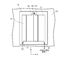
図1は、本発明の第1の実施形態に係るプラズマアクチュエータの概略構成を示す断面図であり、図2は、平面図である。図1および図2を参照するに、プラズマアクチュエータ10は、対象物、例えば車両の筐体CSの表面に装着される。プラズマアクチュエータ10は、誘電体層11と、誘電体層11の表面に設けた表面電極12と、誘電体層11の裏面側に、表面電極12から表面に沿った誘起流れを生成する方向に設けられた裏面電極13と、表面電極12と裏面電極13との間に設けられた浮遊導電体対14と、裏面電極13に配線18を介して出力部19aが接続された高電圧高周波電源19とを有し、表面電極12は配線16を介して接地されている。
FIG. 1 is a cross-sectional view showing a schematic configuration of a plasma actuator according to a first embodiment of the invention, and FIG. 2 is a plan view. Referring to FIGS. 1 and 2, the
浮遊導電体対14は、誘電体層11の表面に配置された表面導電体14aと誘電体層11の裏面側に配置された裏面導電体14bと、表面導電体14aと裏面導電体14bとを電気的に接続する配線部14cとを有する。表面導電体14aおよび裏面導電体14bは、誘電体層11および封止層15により表面電極12および裏面電極13とは電気的に絶縁され、配線部14c、例えばスルーホールによって電気的に接続され同電位になる。浮遊導電体対14、つまり表面導電体14aおよび裏面導電体14bは電気的に浮いた状態である。
The
プラズマアクチュエータ10は、平面視において、誘起流れを発生させる方向(図1および図2に示すX方向)に、表面電極12、裏面導電体14b、表面導電体14aおよび裏面電極13の順に配置される。表面電極12、裏面電極13、裏面導電体14bおよび表面導電体14aは、誘起流れを生成する範囲に応じて、筐体CSの表面に沿って、例えば、図2に示すように、X方向とは直角をなすY方向に延在する。
表面導電体14aと表面電極12との間隙、すなわち、表面導電体14aの後端部と表面電極12との先端部との間隙が、裏面導電体14bと表面電極12との間隙、すなわち、裏面導電体14bの後端部と表面電極12との先端部との間隙よりも大きい方が図3で説明する電荷分布が良好な点で、好ましい。
The gap between the
表面導電体14aの幅は、表面電極12の幅と同じかそれよりも短い方が誘起流れを円滑に加速できる点で好ましい。幅はX方向の長さを示す。
The width of the
高電圧高周波電源19は、高周波あるいはパルス状の高電圧信号を供給可能な電源であれば特に限定されない。この高電圧信号は、高周波あるいはパルス状であり、周波数が、電源の装置コストを考慮した実用的な観点から、0.05kHz~1000kHzに設定されることが好ましく、電圧が0.1kV~100kVに設定されることが好ましい。
The high-voltage high-
表面電極12、裏面電極13、裏面導電体14bおよび表面導電体14aは、その形態は特に限定されない。表面電極12および表面導電体14aは、誘電体層11にフラッシュマウント化され、その表面が露出するように配置されることが、誘電体層の表面に円滑な誘起流れを形成する点で好ましい。裏面電極13および裏面導電体14bは、誘電体層11と封止層15とに覆われることで、裏面側に、DBD、スパークおよびコロナ放電の発生を防止する点で好ましい。なお、裏面電極13および裏面導電体14bは、誘電体層11に埋め込まれるように形成してもよい。
The form of the
プラズマアクチュエータ10は、筐体の表面から突出しない方が好ましく、その観点から、表面電極12、裏面電極13、裏面導電体14および表面導電体15は、金属材料、例えば銅、アルミニウム、金、銀および導電性酸化物、例えば酸化インジウムスズ(ITO)で形成された薄板状または薄膜状であることが好ましい。誘電体層11は、例えば、アクリル樹脂、シリコーンゴム、シリコーン樹脂、アルミナセラミックス、サファイア(高純度アルミナセラミックス)、ポリイミド、ポリテトラフルオロエチレン(PTFE)樹脂(例えばテフロン(登録商標))、PET(ポリエチレンテレフタレート)樹脂、パイレック(登録商標)スガラス、石英ガラス、PEEK、各種油脂などを用いることができる。封止層15は、例えば、レジスト、シリコーンゴム、ポリイミド、PTFE樹脂(例えばテフロン(登録商標))などのコーティング・封止材料を用いることができる。封止層15は、接着性剤を用いてもよく、これによってプラズマアクチュエータ10を筐体CSの表面に接着してもよい。また、封止層15と筐体CSの表面との間に接着層を設けてもよい。
It is preferable that the
プラズマアクチュエータ10は、表面電極12を接地して、裏面電極13を高電圧高周波電源19の出力部19aに電気的に接続する。高電圧高周波電源19は接地しているので、出力部19aから±Vp(Vpは交流電圧の片側振幅を表す。)の電圧の正弦波の高電圧信号を裏面電極13に印加することで、例えば、表面電極12と裏面導電体14bとの間におおよそ±1/2Vpの電圧が印加され、それとともに、表面導電体14aと裏面電極13との間におおよそ±1/2Vpの電圧が印加される。これにより、表面電極12と、裏面導電体14bとの間の誘電体層11の表面と、表面導電体14aと裏面電極13との間の誘電体層11の表面に誘電体バリア放電(DBD、(Dielectric Barrier Discharge))が生成される。DBDにより誘起流れIFが発生する。なお、表面電極12と裏面導電体14bとの間の電圧および表面導電体14aと裏面電極13との間の電圧は、表面電極12、裏面導電体14b、表面導電体14aおよび裏面電極13の平面視した場合の重なり具合や表面電極12と裏面導電体14bとの間および表面導電体14aと裏面電極13との間の誘電体層11の厚さに応じて異なるので、これらにより誘起流れIFの発生の制御を行ってもよい。
The
上記の説明では、プラズマアクチュエータ10は、表面電極12を接地し、裏面電極13を高電圧高周波電源19の出力部19aに電気的に接続したが、逆に裏面電極13を接地し、表面電極12を高電圧高周波電源19の出力部19aに接続してもよい。この場合でも、同じ電圧印加条件において概ね同程度の誘起流れ速度が得られることが実験で示されている。
In the above description, the
図3は、本発明の第1の実施形態に係るプラズマアクチュエータの動作の説明図である。図3(a)は、裏面電極13に+Vpの電圧が印加された場合、図3(b)は、裏面電極13に-Vpの電圧が印加された場合の電荷の分布を示している。
FIG. 3 is an explanatory diagram of the operation of the plasma actuator according to the first embodiment of the present invention. 3A shows the charge distribution when a voltage of +Vp is applied to the
図3(a)を参照するに、裏面電極13に+Vpの電圧が印加され、表面電極12が接地されているので、裏面電極13から表面電極12へ方向の電界が発生する。表面電極12と裏面電極13との間にある浮遊導電体対14は、例えばおおよそ+1/2Vpの電位となる。これにより、裏面電極13の後端部13TR側(-X方向)に正電荷が移動し、表面導電体14aの先端部14aLDに負電荷が移動し、裏面導電体14bの後端部14bTR側(-X方向)に正電荷が移動し、表面電極12の先端部12LD側(X方向)に負電荷が移動する。このようにして生じた電位差により、表面電極12の先端部12LDの近傍に電界(大きさはおおよそ-dVp/dxとなる。)が形成される。作動流体(空気等)が部分的に絶縁破壊する程度の電界により、表面電極12と裏面導電体14bとの間の誘電体層11の表面にDBDが生成される。これと同様にして、表面導電体14aと裏面電極13との間の誘電体層11の表面にDBDが生成される。DBDにより作動流体の一部がイオン化して荷電粒子が生成される。荷電粒子は電界によって発生する体積力により加速される。荷電粒子とイオン化されていない中性粒子との衝突が繰り返し行われ、その結果、巨視的な誘起流れIFが発生する。誘起流れIFの方向は、表面電極12から裏面導電体14bへの方向であり、表面導電体14aから裏面電極13への方向である。両方のDBDが同じ方向(X方向)の流れを誘起する。Referring to FIG. 3(a), since a voltage of +Vp is applied to the
他方、表面導電体14aと裏面導電体14bは配線部14cで接続されているので同電位となり、表面導電体14aと裏面導電体14bと間ではDBDは生成されない。つまり、表面導電体14aと裏面導電体14bとによって表面導電体14aの後端部14aTRから-X方向にはDBDが生成されない。そのため、表面導電体14aから裏面導電体14bの方向への誘起流れは発生しない。これにより、従来問題となっていた複数の表面電極の存在による互いに衝突する誘起流れ、いわゆるクロストークの問題は、本実施形態のプラズマアクチュエータ10により解決することができる(クロストークについては、例えば、H. Do et al., Applied Physics Letters, 2008, Vol. 92, 071504参照。)。On the other hand, since the
図3(b)を参照するに、裏面電極13に-Vpの電圧が印加され、表面電極12が接地されているので、浮遊導電体対14は、例えば-1/2Vpの電位となる。電荷の分布は、図3(a)と逆になる。DBDは、図3(a)と同様に、表面電極12と裏面導電体14bとの間の誘電体層11の表面にDBDが生成され、表面導電体14aと裏面電極13との間の誘電体層11の表面にDBDが生成され、表面導電体14aと裏面導電体14bと間ではDBDは生成されない。DBDにより発生する誘起流れIFの方向は、表面電極12から裏面導電体14bへの方向であり、表面導電体14aから裏面電極13への方向である。両方のDBDが同じ方向(X方向)の流れを誘起する。
Referring to FIG. 3(b), since a voltage of -Vp is applied to the
したがって、±Vpの電圧の高周波電圧が印加されることによって、プラズマアクチュエータ10により、表面電極12と裏面導電体14bとの間の誘電体層11の表面にDBDが生成され、表面導電体14aと裏面電極13との間の誘電体層11の表面にDBDが生成され、これらのDBDによって発生する誘起流れは、表面電極12から裏面電極13の方向に発生する。
Therefore, by applying a high-frequency voltage of ±Vp, the
本実施形態によれば、表面電極12と裏面電極13との間に、電気的に互いに接続された表面導電体14aと裏面導電体14bとを有する浮遊導電体対14を設けたことで、高電圧高周波電源19により表面電極12と裏面電極13との間に高周波高電圧を印加すると、表面電極12と裏面導電体14bとの間の表面および表面導電体14aと裏面電極13との間の表面の2か所においてDBDが生成される。表面電極12から裏面導電体14bへの方向と表面導電体14aから裏面電極13への方向が同一方向であるので、表面電極12と裏面導電体14bとの間の表面で生成されたDBDにより発生した誘起流れが、表面導電体14aと裏面電極13との間の表面において生成されたDBDにより発生した誘起流れによって加速される。これにより、プラズマアクチュエータ10は、効率良く誘起流れの速度を高めることができる。
According to the present embodiment, the floating
図4は、本発明の第1の実施形態に係るプラズマアクチュエータの変形例の概略構成を示す断面図である。図4を参照するに、プラズマアクチュエータ50は、誘電体層11と、誘電体層11の表面に設けた表面電極52と、誘電体層11の裏面に、表面電極12から表面に沿った誘起流れを発生させる方向(X方向)に設けられた裏面電極13と、表面電極52と裏面電極13との間に設けられた浮遊導電体対54と、表面電極52と裏面電極13とに配線16,18を介して接続された高電圧高周波電源19とを有する。浮遊導電体対54は、表面導電体54aと裏面導電体54bと、表面導電体54aと裏面導電体54bとを電気的に接続する配線部54cとを有する。プラズマアクチュエータ50は、図1に示したプラズマアクチュエータ10の変形例である。表面電極52および表面導電体54aは、X方向に沿った断面がそれぞれ先端部52LD、54aLDに向かって次第に狭く形成される。これにより、表面電極の先端部52LDおよび表面導電体の先端部54aLDの電荷密度が増加し、その表面の電界強度が増加するので、プラズマアクチュエータ50は、より低い電圧でもDBDが生成し易くなり、印加する電圧を抑制できる。FIG. 4 is a cross-sectional view showing a schematic configuration of a modification of the plasma actuator according to the first embodiment of the present invention. Referring to FIG. 4, the
なお、プラズマアクチュエータ50は、裏面電極13を接地し、表面電極52を高電圧高周波電源19の出力部19aに接続してもよい。この場合でも、同じ電圧印加条件において概ね同程度の誘起流れ速度が得られることが実験で示されている。
The
図5は、本発明の第1の実施形態に係るプラズマアクチュエータの他の変形例の概略構成を示す断面図である。図5を参照するに、プラズマアクチュエータ100は、誘電体層11と、誘電体層11の表面に設けた表面電極12と、誘電体層11の裏面に、表面電極12から表面に沿った誘起流れを生成する方向(X方向)に設けられた裏面電極13と、表面電極12と裏面電極13との間に設けられた2つの浮遊導電体対14、114と、裏面電極13に配線18を介して出力部19aが接続された高電圧高周波電源19とを有し、表面電極12は配線16を介して接地されている。プラズマアクチュエータ100は、図1および2に示したプラズマアクチュエータ10の変形例であり、浮遊導電体対14と裏面電極13との間に浮遊導電体対114をさらに設けたものである。プラズマアクチュエータ110は、プラズマアクチュエータ10と同様の構成については説明を省略する。
FIG. 5 is a cross-sectional view showing a schematic configuration of another modification of the plasma actuator according to the first embodiment of the present invention. Referring to FIG. 5, the
浮遊導電体対114は、浮遊導電体対14と同様の構成を有する。浮遊導電体対114は、誘電体層11の表面に配置された表面導電体114aと誘電体層11の裏面側に配置された裏面導電体114bと、表面導電体114aと裏面導電体114bとを電気的に接続する配線部114cとを有する。表面導電体114aおよび裏面導電体114bは、誘電体層11および封止層15により表面電極12および裏面電極13とは電気的に絶縁され、配線部114c、例えばスルーホールによって電気的に接続され同電位になる。浮遊導電体対114は電気的に浮いた状態である。
Floating
プラズマアクチュエータ100は、表面電極12を配線16を介して接地して、裏面電極13を高電圧高周波電源19の出力部19aに電気的に接続する。高電圧高周波電源19は接地しているので、出力部19aから±Vpの電圧の正弦波の高電圧信号を裏面電極13に印加することで、例えば、表面電極12と、裏面導電体14bとの間におおよそ±1/3Vpの電圧が印加され、表面導電体14aと裏面導電体114bとの間におおよそ±1/3Vpの電圧が印加され、表面導電体114aと裏面電極13との間におおよそ±1/3Vpの電圧が印加される。これにより、表面電極12と裏面導電体14bとの間の誘電体層11の表面と、表面導電体14aと裏面導電体114bとの間の誘電体層11の表面と、表面導電体114aと裏面電極13との間の誘電体層11の表面にDBDが生成される。表面電極12と裏面導電体14bとの間の誘電体層11の表面で生成されたDBDにより発生した誘起流れIFは、X方向に沿った他の2つのDBDにより発生した誘起流れによってX方向の誘起流れIFが加速される。これにより、プラズマアクチュエータ100は、効率良く誘起流れIFの速度を高めることができる。
The
なお、プラズマアクチュエータ100は、浮遊導電体対14および浮遊導電体対114を含むが、浮遊導電体対をさらに設けてもよい。これにより、DBDの生成箇所を増やして、誘起流れIFの速度をさらに高めることができる。
プラズマアクチュエータ100は、裏面電極13を接地し、表面電極12を高電圧高周波電源19の出力部19aに接続してもよい。この場合でも、同じ電圧印加条件において概ね同程度の誘起流れ速度が得られることが実験で示されている。
The
図6は、本発明の第2の実施形態に係るプラズマアクチュエータの概略構成を示す断面図である。図6を参照するに、プラズマアクチュエータ200は、図1に示したプラズマアクチュエータ10を2つ組み合わせた構成を有し、高電圧高周波電源19の出力部19aが近接する2つの電極(裏面電極13および表面電極212)に電気的に接続された構成を有する。プラズマアクチュエータ200は、誘電体層11と、誘電体層11の表面に設けられた表面電極12および表面電極212と、誘電体層11の裏面側に設けられた裏面電極13および裏面電極213とを含み、平面視において表面電極12から誘起流れを発生させる方向(X方向)に裏面電極13、表面電極212および裏面電極213の順に配置される。
FIG. 6 is a cross-sectional view showing a schematic configuration of a plasma actuator according to a second embodiment of the invention. Referring to FIG. 6, the
プラズマアクチュエータ200は、表面電極12と裏面電極13との間に浮遊導電体対14と、表面電極212と裏面電極213との間に浮遊導電体対214とを含む。浮遊導電体対214は、浮遊導電体対14と同様の構成を有する。浮遊導電体対214は、誘電体層11の表面に配置された表面導電体214aと誘電体層11の裏面側に配置された裏面導電体214bと、表面導電体214aと裏面導電体214bとを電気的に接続する配線部214cとを有する。表面導電体214aおよび裏面導電体214bは、誘電体層11および封止層15により表面電極212および裏面電極213とは電気的に絶縁され、配線部214c、例えばスルーホールによって電気的に接続され同電位になる。浮遊導電体対214は電気的に浮いた状態である。
裏面電極13は、高電圧高周波電源19の出力部19aに配線18を介して電気的に接続される。表面電極212は、配線部218、裏面電極13および配線18を介して高電圧高周波電源19の出力部19aに電気的に接続される。表面電極12は配線16を介して接地され、裏面電極213は配線216を介して接地される。
The
プラズマアクチュエータ200は、高電圧高周波電源19の出力部19aから高周波高電圧を裏面電極13および表面電極212に印加することで、表面電極12と裏面導電体14bとの間の誘電体層11の表面と、表面導電体14aと裏面電極13との間の誘電体層11の表面と、表面電極212と裏面導電体214bとの間の誘電体層11の表面と、表面導電体214aと裏面電極13との間の誘電体層11の表面にDBDが生成され、DBDにより誘起流れIFが発生する。第1の実施形態で説明したように、各々のDBDにより全て同じ方向に誘起流れIFが発生するので、誘起流れIFは加速され、プラズマアクチュエータ200は、効率良く誘起流れの速度を高めることができる。
The
なお、プラズマアクチュエータ200は、浮遊導電体対14および浮遊導電体対214はそれぞれ1対を含むが、それぞれ複数の浮遊導電体対をさらに設けてもよい。これにより、DBDの生成箇所を増やして、誘起流れIFの速度をさらに高めることができる。
プラズマアクチュエータ200は、裏面電極13を接地し、表面電極12および裏面電極213を高電圧高周波電源19の出力部19aに接続してもよい。この場合でも、同じ電圧印加条件において概ね同程度の誘起流れ速度が得られることが実験で示されている。
The
図7は、本発明の第3の実施形態に係るプラズマアクチュエータの概略構成を示す断面図であり、図8は平面図である。図7および図8を参照するに、プラズマアクチュエータ300は、誘電体層11と、誘電体層11の表面に設けられた表面電極12と、表面電極12から表面に沿った誘起流れを生成する方向(X方向)に誘電体層11の裏面側に設けられた裏面電極13と、表面電極12と裏面電極13との間に設けられた浮遊導電体対314と、裏面電極13に配線18を介して出力部19aが接続された高電圧高周波電源19とを有し、表面電極12は配線16を介して接地されている。表面電極12、裏面電極13および浮遊導電体対314はY方向に延在する。プラズマアクチュエータ300は、図1に示した第1の実施形態のプラズマアクチュエータ10の変形例であり、浮遊導電体対314が異なっている以外は同様に構成されている。
FIG. 7 is a cross-sectional view showing a schematic configuration of a plasma actuator according to a third embodiment of the invention, and FIG. 8 is a plan view. 7 and 8, the
浮遊導電体対314は、表面導電体81と、誘電体材料の被覆部材82に覆われた導電線83からなる被覆導線84を複数配列し帯状に形成してそれぞれの導電線83の一端を互いに電気的に接続した被覆導線帯85と、表面導電体81と被覆導線帯85の導電線83とを電気的に接続する配線部86からなる。被覆導線帯85は、導電線83が誘電体材料の被覆部材82に覆われているのでその表面が電気的に絶縁されている。被覆導線帯85は、図7および図8に示すように、誘電体層11にフラッシュマウント化されてもよく、誘電体層11の表面に配置してもよく、誘電体層11の表面にY方向に延在する凹部を形成し、凹部内に配置してもよい。
The floating
被覆部材82は、特に限定されないが、PTFE樹脂(例えばテフロン(登録商標))、シリコーン樹脂等の可撓性を有する材料を用いることが、3次元形状の筐体の表面に設置しやすい点で、好ましい。導電線83は、銅、金、銀、タングステン、チタン、ステンレススチール(SUS)、ニッケル等の金属材料を用いることができる。なお、導電線83は、図7に示したように断面形状が円形でもよく楕円形でもよく、薄帯状で断面形状が長方形でもよい。薄帯状の場合は、導電性酸化物、例えばITOを用いることができる。
The coating
浮遊導電体対314は、表面導電体81と被覆導線帯85の導電線83とが配線部86によって電気的に接続され同電位になる。浮遊導電体対314は電気的に浮いた状態である。
In the floating
プラズマアクチュエータ300は、第1の実施形態の図1および図2に示したプラズマアクチュエータ10における裏面導電体14を被覆導線帯85に置換した構成を有する。したがって、プラズマアクチュエータ300は、プラズマアクチュエータ10と同様の作用および効果を有し、その詳細な説明を省略する。さらに、プラズマアクチュエータ300は、被覆導線帯85を用いることで、裏面導電体を用いた場合のような電気的に絶縁する手間を省略でき、外部あるいは筐体の導電部材との短絡を回避することができる。
The
プラズマアクチュエータ300は、裏面電極13を接地し、表面電極12および裏面電極213を高電圧高周波電源19の出力部19aに接続してもよい。この場合でも、同じ電圧印加条件において概ね同程度の誘起流れ速度が得られることが実験で示されている。
The
図9は、本発明の第4の実施形態に係るプラズマアクチュエータの概略構成を示す断面図である。図9を参照するに、プラズマアクチュエータ350は、誘電体層11と、誘電体層11の表面に設けられた表面電極12と、表面電極12から表面に沿った誘起流れを生成する方向(X方向)に誘電体層11の裏面側に設けられた裏面電極としての被覆導線帯353と、表面電極12と被覆導線帯353との間に設けられた浮遊導電体対14と、被覆導線帯353に配線18を介して出力部19aが接続された高電圧高周波電源19とを有し、表面電極12は配線16を介して接地されている。表面電極12、被覆導線帯353および浮遊導電体対14はY方向に延在する。プラズマアクチュエータ350は、図1に示した第1の実施形態のプラズマアクチュエータ10の変形例であり、裏面電極が、被覆導線帯353となっている以外は同様に構成されている。
FIG. 9 is a cross-sectional view showing a schematic configuration of a plasma actuator according to a fourth embodiment of the invention. Referring to FIG. 9, the
被覆導線帯353は、誘電体材料の被覆部材82に覆われた導電線83からなる被覆導線84を複数配列し帯状に形成してそれぞれの導電線83の一端を互いに電気的に接続したものである。被覆導線帯353は、導電線83が誘電体材料の被覆部材82に覆われているのでその表面が電気的に絶縁されている。被覆導線帯353は、誘電体層11にフラッシュマウント化されてもよく、誘電体層11の表面に配置してもよく、誘電体層11の表面にY方向に延在する凹部を形成し、凹部内に配置してもよい。
The covered
被覆導線帯353は、被覆導線帯85の導電線83に高電圧高周波電源19の出力部19aが接続されているので、表面電極12との間に高周波高電圧が印加される。プラズマアクチュエータ350は、第1の実施形態の図1および図2に示したプラズマアクチュエータ10における裏面電極13を被覆導線帯85に置換した構成を有する。したがって、プラズマアクチュエータ350は、プラズマアクチュエータ10と同様の作用および効果を有し、その詳細な説明を省略する。さらに、プラズマアクチュエータ350は、被覆導線帯353を用いることで、裏面導電体を用いた場合のような電気的に絶縁する手間を省略でき、外部あるいは筐体の導電部材との短絡を回避することができる。
Since the
なお、プラズマアクチュエータ350は、図7に示したプラズマアクチュエータ300のように、浮遊導電体対14の裏面導電体に被覆導線帯85を用いてもよい。これにより、裏面導電体および裏面電極の電気的な絶縁のための封止層15を用いなくてもよく、プラズマアクチュエータの筐体CSへの取り付けが容易になる。
The
プラズマアクチュエータ350は、被覆導線帯353の導電線83を接地し、表面電極12を高電圧高周波電源19の出力部19aに接続してもよい。この場合でも、同じ電圧印加条件において概ね同程度の誘起流れ速度が得られることが実験で示されている。
The
図10は、本発明の第4の実施形態に係るプラズマアクチュエータの変形例の概略構成を示す断面図である。図10を参照するに、プラズマアクチュエータ400は、誘電体層11と、誘電体層11の表面に設けられた表面電極12と、表面電極12から表面に沿った誘起流れを生成する方向(X方向)に誘電体層11の裏面側に設けられた裏面電極としての被覆導線帯353と、表面電極12と被覆導線帯353との間に設けられた浮遊導電体対14および114と、被覆導線帯353に配線18を介して出力部19aが接続された高電圧高周波電源19とを有し、表面電極12は配線16を介して接地されている。表面電極12、被覆導線帯353および浮遊導電体対14、114はY方向に延在する。プラズマアクチュエータ400は、図9に示した第4の実施形態のプラズマアクチュエータ350の変形例であり、浮遊導電体対114が、浮遊導電体対14と被覆導線帯353との間に追加された以外は同様に構成されている。また、プラズマアクチュエータ400は、図5に示した第1の実施形態に係るプラズマアクチュエータの他の変形例のプラズマアクチュエータ100の変形例であり、裏面電極13を被覆導線帯353とした以外は同様に構成されている。したがって、プラズマアクチュエータ400は、プラズマアクチュエータ100と同様の作用および効果を有し、その詳細な説明を省略する。さらに、プラズマアクチュエータ400は、被覆導線帯353を用いることで、裏面導電体を用いた場合のような電気的に絶縁する手間を省略でき、外部あるいは筐体の導電部材との短絡を回避することができる。
FIG. 10 is a cross-sectional view showing a schematic configuration of a modification of the plasma actuator according to the fourth embodiment of the invention. Referring to FIG. 10, the
プラズマアクチュエータ400は、被覆導線帯353の導電線83を接地し、表面電極12を高電圧高周波電源19の出力部19aに接続してもよい。この場合でも、同じ電圧印加条件において概ね同程度の誘起流れ速度が得られることが実験で示されている。
The
図11は、本発明の第5の実施形態に係るプラズマアクチュエータの概略構成を示す断面図である。図11を参照するに、プラズマアクチュエータ500は、図9に示したプラズマアクチュエータ350を2つ組み合わせた構成を有し、高電圧高周波電源19の出力部19aが近接する2つの電極(裏面電極としての被覆導線帯353および表面電極212)に電気的に接続された構成を有する。プラズマアクチュエータ500は、誘電体層11と、誘電体層11の表面に設けられた表面電極12および表面電極212と、誘電体層11の裏面側に設けられた被覆導線帯353および裏面電極213とを含み、平面視において表面電極12から誘起流れを発生させる方向(X方向)に裏面電極13、表面電極212および裏面電極213の順に配置される。
FIG. 11 is a cross-sectional view showing a schematic configuration of a plasma actuator according to a fifth embodiment of the invention. Referring to FIG. 11, the
プラズマアクチュエータ500は、表面電極12と被覆導線帯353との間に浮遊導電体対14と、表面電極212と裏面電極213との間に浮遊導電体対214とを含む。浮遊導電体対14および214の構成は、図6に示した第2の実施形態に係るプラズマアクチュエータ200と同様である。
プラズマアクチュエータ500は、図6に示した第2の実施形態に係るプラズマアクチュエータ200の裏面電極13を被覆導線帯353に置換した構成を有する。したがって、プラズマアクチュエータ500は、プラズマアクチュエータ200と同様の作用および効果を有し、その詳細な説明を省略する。さらに、プラズマアクチュエータ500は、被覆導線帯353を用いることで、裏面電極を用いた場合のような電気的に絶縁する手間を省略でき、外部あるいは筐体の導電部材との短絡を回避することができる。
A
プラズマアクチュエータ500は、被覆導線帯353の導電線83を接地し、表面電極12および裏面電極213を高電圧高周波電源19の出力部19aに接続してもよい。この場合でも、同じ電圧印加条件において概ね同程度の誘起流れ速度が得られることが実験で示されている。
The
図1および図2に示した第1の実施形態に係るプラズマアクチュエータ10を用いて誘起流れの流動特性を得た。実施例1として、誘電体層は厚さ0.4mmのシリコーン樹脂板、表面電極、裏面電極、表面導電体および裏面導電体は、幅(X方向)がそれぞれ、6mm、9.5mm、6mm、9.5mm、長さ(Y方向)が80mm、厚さが17μmの銅箔を用いた。なお、表面電極および表面導電体はシリコーン樹脂板上に形成した。
Flow characteristics of the induced flow were obtained using the
比較例として、表面電極および裏面電極からなるプラズマアクチュエータを用いた。誘電体層は厚さ0.4mmのシリコーン樹脂板、表面電極および裏面電極は、幅(X方向)がそれぞれ、5mm、15mm、長さ(Y方向)が100mm、厚さが17μmの銅箔を用いた。なお、表面電極はシリコーン樹脂板上に形成した。 As a comparative example, a plasma actuator composed of a front electrode and a back electrode was used. The dielectric layer is a silicone resin plate with a thickness of 0.4 mm, and the front and back electrodes are copper foils with a width (X direction) of 5 mm and 15 mm, a length (Y direction) of 100 mm, and a thickness of 17 μm. Using. The surface electrodes were formed on a silicone resin plate.
高電圧高周波電源は、松定プレシジョン社製モデルHAPS-10B40を使用して印加電圧Vpを2.5kVから9.0kV、周波数10kHzの正弦波の電圧を実施例1および比較例の表面電極と裏面電極との間に印加した。 As a high-voltage high-frequency power supply, a model HAPS-10B40 manufactured by Matsusada Precision Co., Ltd. is used to apply an applied voltage Vp of 2.5 kV to 9.0 kV and a sine wave voltage with a frequency of 10 kHz. applied between the electrodes.
図12は、実施例1のプラズマアクチュエータの誘起流れの速度分布図である。速度分布図の横軸は、プラズマアクチュエータの長さ方向(X方向)を示しており、速度分布図の下に、対応するプラズマアクチュエータの構成を示している。表面電極12の先端部はX=6.2mm、表面導電体14aの先端部はX=21.7mmである。縦軸は高さ方向を示しており、誘電体層表面は2mmの位置である。速度分布図は、誘起流れの方向を矢印の方向で示し、誘起流れの速度を矢印の長さおよび濃淡で示す。その濃淡と速度との関係を速度分布図の右に示す。誘起流れの速度分布は、粒子画像流速測定法(PIV(Particle Image Velocimetry))により解析した。
12 is a velocity distribution diagram of the induced flow of the plasma actuator of Example 1. FIG. The horizontal axis of the velocity distribution diagram indicates the length direction (X direction) of the plasma actuator, and the configuration of the corresponding plasma actuator is shown below the velocity distribution diagram. The tip of the
図12を参照するに、表面電極12の先端部付近の誘電体層の表面付近からX方向の誘起流れが生じ、表面導電体14aの先端部付近から誘起流れの速度が増加していることが分かる。最大誘起流れ速度umaxの評価位置は表面電極12の先端部から25mm(X=31.2mm)の位置であり、umax(300回平均値)は1.06m/sであった。このときの消費電力は49.8W/mであった。Referring to FIG. 12, an induced flow in the X direction is generated near the surface of the dielectric layer near the tip of the
図13は、比較例のプラズマアクチュエータの誘起流れの速度分布図である。速度分布図は図12と同様に示している。表面電極12の先端部はX=7.2mmである。誘電体層表面は高さ2mmの位置である。
FIG. 13 is a velocity distribution diagram of the induced flow of the plasma actuator of the comparative example. A velocity distribution map is shown in the same manner as in FIG. The tip of the
図13を参照するに、表面電極の先端部付近の誘電体層の表面付近からX方向の誘起流れが生じ、先端部から13mm(X=20mm)の位置ではほぼ誘起流れの速度が飽和していることが分かる。最大誘起流れ速度umaxの評価位置は表面電極の先端部から25mm(X=32.2mm)の位置であり、umax(300回平均値)は0.62m/sであった。このときの消費電力は44.2W/mであった。Referring to FIG. 13, an induced flow in the X direction is generated near the surface of the dielectric layer near the tip of the surface electrode, and the velocity of the induced flow is almost saturated at a
図14は、実施例1および比較例のプラズマアクチュエータの誘起流れの最大速度umaxと消費電力の関係を示す図である。種々の消費電力における誘起流れの速度分布図を測定し、図12および図13に示した評価位置における最大誘起流れ速度umaxを得た。FIG. 14 is a diagram showing the relationship between the maximum velocity u max of the induced flow and the power consumption of the plasma actuators of Example 1 and Comparative Example. The velocity profiles of the induced flow at various power consumptions were measured, and the maximum induced flow velocity u max at the evaluation positions shown in FIGS. 12 and 13 was obtained.
図14を参照するに、消費電力が80W/m以下では、明らかに実施例1が比較例よりも消費電力に対する誘起流れの速度が高まっていることが分かる。この範囲において、線形回帰式を求めて同じ消費電力で比較すると、実施例1が比較例よりも約1.5倍の速度になっていることが分かった。これにより、実施例1が比較例よりも高効率化されていることが分かる。 As can be seen from FIG. 14, when the power consumption is 80 W/m or less, the speed of the induced flow relative to the power consumption is clearly higher in Example 1 than in the comparative example. In this range, when a linear regression formula was calculated and compared with the same power consumption, it was found that the speed of Example 1 was about 1.5 times faster than that of the comparative example. From this, it can be seen that the efficiency of Example 1 is higher than that of the comparative example.
実施例2として、図6に示した第2の実施形態に係るプラズマアクチュエータ200を用いて誘起流れの流動特性を得た。実施例2は、誘電体層、表面電極、裏面電極、表面導電体および裏面導電体の材料および大きさを実施例1と同様とした。表面電極および表面導電体はシリコーン樹脂板上に形成した。高電圧高周波電源は、ピー・エス・アイ社製、モデルPSI-PG109R5Mを使用して印加電圧Vpを9.0kV、周波数9.6kHzの疑似矩形波の電圧を表面電極12と裏面電極13との間および表面電極212と裏面電極213との間に印加した。
As Example 2, the flow characteristics of the induced flow were obtained using the
図15は、実施例2のプラズマアクチュエータの誘起流れの速度分布図である。速度分布図は、図12および図13と同様の仕様である。誘電体層表面は高さ方向2mmの位置である。 15 is a velocity distribution diagram of the induced flow of the plasma actuator of Example 2. FIG. The velocity distribution map has the same specifications as those in FIGS. 12 and 13. FIG. The dielectric layer surface is located at a height of 2 mm.
図15を参照するに、表面電極12の先端部付近の誘電体層の表面付近からX方向の誘起流れが生じ、表面導電体14a、表面電極212、表面導電体214aのそれぞれの先端部付近から誘起流れの速度が増加していることが分かる。これにより、第2の実施形態に係るプラズマアクチュエータ200の構成により、誘起流れを加速できることが分かった。
Referring to FIG. 15, an induced flow in the X direction is generated from near the surface of the dielectric layer near the tip of the
以上、本発明の好ましい実施形態について詳述したが、本発明は係る特定の実施形態に限定されるものではなく、特許請求の範囲に記載された本発明の範囲内において、種々の変形・変更が可能である。例えば、各実施形態のプラズマアクチュエータを互いに組み合わせてもよい。 Although the preferred embodiments of the present invention have been described in detail above, the present invention is not limited to such specific embodiments, and various modifications and changes can be made within the scope of the present invention described in the claims. is possible. For example, the plasma actuators of each embodiment may be combined with each other.
本発明のプラズマアクチュエータは、乗用車、高速列車、航空機等の移動体に適用することができる。また、本発明のプラズマアクチュエータは、流体機械、例えばタービン、風力発電機の風車等の高速回転体のブレードに適用することができる。 The plasma actuator of the present invention can be applied to moving bodies such as passenger cars, high-speed trains, and aircraft. Also, the plasma actuator of the present invention can be applied to blades of high-speed rotating bodies such as fluid machines such as turbines and windmills of wind power generators.
なお、以上の説明に関してさらに実施形態として以下の付記を開示する。
(付記1) 誘起流れを生成可能なプラズマアクチュエータであって、
誘電体層と、
前記誘電体層の表面に設けられた第1の電極と、
前記誘電体層の裏面側に、前記第1の電極から一方向に設けられた第2の電極と、
前記第1の電極と前記第2の電極との間に設けられ、前記誘電体層の表面に配置された表面導電体と前記誘電体層の裏面側に配置された裏面導電体とを有する浮遊導電体対であって、該表面導電体と該裏面導電体とは互いに電気的に接続され、前記第1の電極および第2の電極とは電気的に絶縁され、平面視において前記第1の電極から前記一方向に、該裏面導電体、該表面導電体の順に配置される、該浮遊導電体対と、
前記第1の電極と前記第2の電極とに接続された電源と、を備え、
前記電源によって前記第1の電極と前記第2の電極との間に高周波高電圧を印加することで、前記第1の電極と前記裏面導電体との間の表面と、前記表面導電体と前記第2の電極との間の表面に誘電体バリア放電を生成して、前記第1の電極から前記一方向に前記誘電体層の表面に沿って前記誘起流れを発生可能な、前記プラズマアクチュエータ。
(付記2) 前記表面導電体と前記第1の電極との間隙長さが、前記裏面導電体と前記第1の電極との間隙長さよりも大きい、付記1記載のプラズマアクチュエータ。
(付記3) 前記表面導電体の幅は、前記第1の電極と同じかそれよりも短い、付記1または2記載のプラズマアクチュエータ。
(付記4) 前記第1の電極および前記表面導電体の少なくとも一方は、その表面が露出するとともに前記誘電体層の表面にフラッシュマウント化されてなる、付記1~3のうち、いずれか一項記載のプラズマアクチュエータ。
(付記5) 前記第1の電極および前記表面導電体の少なくとも一方は、前記一方向に沿った断面が該一方向の先端部に向かって次第に狭く形成されてなる、付記1~4のうち、いずれか一項記載のプラズマアクチュエータ。
(付記6) 前記浮遊導電体対と前記第2の電極との間に、前記誘電体層の表面に配置された他の表面導電体と前記誘電体層の裏面側に配置された他の裏面導電体とを有する他の浮遊導電体対を少なくとも一つさらに備え、平面視において前記第1の電極から前記一方向に、前記裏面導電体、前記表面導電体、該他の裏面導電体、該他の表面導電体の順に配列される、付記1~5のうちいずれか一項記載のプラズマアクチュエータ。
(付記7) 前記他の表面導電体は、前記一方向に沿った断面が該一方向の先端部に向かって次第に狭く形成されてなる、付記6記載のプラズマアクチュエータ。
(付記8) 前記第2の電極および前記裏面導電体の少なくとも一方は、誘電体材料に覆われた導電線を有する被覆導線を複数配列した被覆導線帯であり、該複数の被覆導線は電気的に互いに接続され、前記誘電体層の表面に前記第1の電極の前記一方向と垂直をなす他の方向に沿って配置してなる、付記1~5のうちいずれか一項記載のプラズマアクチュエータ。
(付記9) 前記被覆導線帯は、前記誘電体層の表面に設けられた凹部に配置してなる、付記8記載のプラズマアクチュエータ。
(付記10) 前記被覆導線帯は、前記誘電体層にフラッシュマウント化してなる、付記8または9記載のプラズマアクチュエータ。
(付記11) 誘起流れを生成可能なプラズマアクチュエータであって、
誘電体層と、
前記誘電体層の表面に設けられた第1および第3の電極と、
前記誘電体層の裏面側に設けられた第2および第4の電極であって、平面視において前記第1の電極から一方向に該第2の電極、前記第3の電極および該第4の電極の順に配置される、該第2および第4の電極と、
前記第1の電極と前記第2の電極との間に設けられ、前記誘電体層の表面に配置された第1の表面導電体と前記誘電体層の裏面側に配置された第1の裏面導電体とを有する第1の浮遊導電体対であって、平面視において前記第1の電極から前記一方向に、該第1の裏面導電体、該第1の表面導電体の順に配置され、該第1の表面導電体と該第1の裏面導電体とは互いに電気的に接続され、前記第1の電極および第2の電極とは電気的に絶縁される、前記第1の浮遊導電体対と、
前記第3の電極と前記第4の電極との間に設けられ、前記誘電体層の表面に配置された第2の表面導電体と前記誘電体層の裏面側に配置された第2の裏面導電体とを有する第2の浮遊導電体対であって、平面視において前記第3の電極から前記一方向に、該第2の裏面導電体、該第2の表面導電体の順に配置され、該第2の表面導電体と該第2の裏面導電体とは互いに電気的に接続され、前記第3の電極および第4の電極とは電気的に絶縁される、前記第2の浮遊導電体対と、
前記第1の電極、前記第2の電極、前記第3の電極および前記第4の電極に接続された電源と、を備え、
前記電源によって前記第1の電極と前記第2の電極との間、および前記第3の電極と前記第4の電極との間に高周波高電圧を印加することにより、前記第1の電極と前記第1の裏面導電体との間、前記第1の表面導電体と前記第2の電極との間、前記第3の電極と前記第2の裏面導電体との間および前記第2の表面導電体と前記第4の電極との間の誘電体層の各表面に誘電体バリア放電を生成して、前記第1の電極から前記一方向に前記誘電体層の表面に沿って前記誘起流れを発生可能な、前記プラズマアクチュエータ。
(付記12) 前記第1の電極、前記第1の表面導電体、前記第3の電極および前記第2の表面導電体の少なくとも一つは、前記誘電体層の表面にフラッシュマウント化されてなる、付記11記載のプラズマアクチュエータ。
(付記13) 前記第1の電極、前記第1の表面導電体、前記第3の電極および前記第2の表面導電体の少なくとも一つは、前記一方向に沿った断面が該一方向の先端部に向かって次第に狭く形成されてなる、付記11または12記載のプラズマアクチュエータ。
(付記14) 前記第1の電極および前記第4の電極は接地され、前記第2の電極および前記第3の電極は前記電源の出力部に接続されてなる、付記11~13のうちいずれか一項記載のプラズマアクチュエータ。
(付記15) 前記第2の電極および前記第4の電極の少なくとも一方は、誘電体材料に覆われた導電線を有する被覆導線を複数配列した被覆導線帯であり、該複数の被覆導線は電気的に互いに接続され、前記誘電体層の表面に前記第1の電極の前記一方向と垂直をなす他の方向に沿って配置してなる、付記11~14のうちいずれか一項記載のプラズマアクチュエータ。
(付記16) 前記第1の裏面導電体および第2の裏面導電体の少なくとも一方は、誘電体材料に覆われた導電線を有する被覆導線を複数配列した被覆導線帯であり、該複数の被覆導線は電気的に互いに接続され、該被覆導線帯が前記誘電体層の表面に前記第1の電極の前記一方向と垂直をなす他の方向に沿って配置してなる、付記11~15のうちいずれか一項記載のプラズマアクチュエータ。
(付記17) 前記被覆導線帯は、前記誘電体層の表面に設けられた凹部に配置してなる、付記15または16記載のプラズマアクチュエータ。
(付記18) 前記被覆導線帯は、前記誘電体層にフラッシュマウント化してなる、付記15~17のうちいずれか一項記載のプラズマアクチュエータ。
(付記19) 前記第1の浮遊導電体対および前記第2の浮遊導電体対の少なくとも一方の前記一方向に、さらに少なくとも一つの他の浮遊導電体対をさらに備える、付記11~18のうちいずれか一項記載のプラズマアクチュエータ。In addition, the following additional remarks are disclosed as further embodiments with respect to the above description.
(Appendix 1) A plasma actuator capable of generating an induced flow,
a dielectric layer;
a first electrode provided on the surface of the dielectric layer;
a second electrode provided on the back side of the dielectric layer in one direction from the first electrode;
A float provided between the first electrode and the second electrode and having a surface conductor arranged on the surface of the dielectric layer and a back conductor arranged on the back surface side of the dielectric layer In a conductor pair, the surface conductor and the back conductor are electrically connected to each other, the first electrode and the second electrode are electrically insulated, and the first the floating conductor pair arranged in the one direction from the electrode in the order of the back conductor and the front conductor;
a power source connected to the first electrode and the second electrode;
By applying a high frequency high voltage between the first electrode and the second electrode by the power supply, the surface between the first electrode and the back conductor, the surface conductor and the The plasma actuator capable of generating a dielectric barrier discharge on the surface between the second electrode to generate the induced flow along the surface of the dielectric layer in the one direction from the first electrode.
(Appendix 2) The plasma actuator according to
(Appendix 3) The plasma actuator according to
(Appendix 4) Any one of
(Appendix 5) Of
(Appendix 6) Between the floating conductor pair and the second electrode, another surface conductor arranged on the surface of the dielectric layer and another back surface arranged on the back surface side of the dielectric layer and at least one other floating conductor pair having a conductor, wherein the rear surface conductor, the front surface conductor, the other rear surface conductor, the rear surface conductor, and the rear surface conductor in the one direction from the first electrode in a plan view. 6. A plasma actuator according to any one of
(Appendix 7) The plasma actuator according to appendix 6, wherein the other surface conductor is formed such that a cross section along the one direction becomes gradually narrower toward a tip portion in the one direction.
(Appendix 8) At least one of the second electrode and the back conductor is a covered conductor band in which a plurality of covered conductors having conductive wires covered with a dielectric material are arranged, and the plurality of covered conductors are electrically and arranged along the other direction perpendicular to the one direction of the first electrode on the surface of the dielectric layer. .
(Appendix 9) The plasma actuator according to appendix 8, wherein the coated conductor band is arranged in a recess provided on the surface of the dielectric layer.
(Appendix 10) The plasma actuator according to appendix 8 or 9, wherein the coated conductor band is flush-mounted on the dielectric layer.
(Appendix 11) A plasma actuator capable of generating an induced flow,
a dielectric layer;
first and third electrodes provided on the surface of the dielectric layer;
A second electrode and a fourth electrode provided on the back surface side of the dielectric layer, wherein the second electrode, the third electrode and the fourth electrode are arranged in one direction from the first electrode in plan view. the second and fourth electrodes arranged in electrode order;
A first surface conductor provided between the first electrode and the second electrode, arranged on the surface of the dielectric layer, and a first back surface arranged on the back surface side of the dielectric layer. a first floating conductor pair having a conductor, wherein the first back conductor and the first surface conductor are arranged in this order in the one direction from the first electrode in a plan view; The first floating conductor, wherein the first surface conductor and the first back surface conductor are electrically connected to each other and electrically insulated from the first electrode and the second electrode. pair and
A second surface conductor provided between the third electrode and the fourth electrode, arranged on the surface of the dielectric layer, and a second back surface arranged on the back surface side of the dielectric layer. a second floating conductor pair having a conductor, wherein the second back conductor and the second front conductor are arranged in this order from the third electrode in the one direction in plan view, The second floating conductor, wherein the second surface conductor and the second back surface conductor are electrically connected to each other and electrically insulated from the third electrode and the fourth electrode. pair and
a power supply connected to the first electrode, the second electrode, the third electrode and the fourth electrode;
By applying a high frequency high voltage between the first electrode and the second electrode and between the third electrode and the fourth electrode by the power supply, the first electrode and the Between the first back surface conductor, between the first surface conductor and the second electrode, between the third electrode and the second back surface conductor, and between the second surface conductor generating a dielectric barrier discharge on each surface of the dielectric layer between the body and the fourth electrode to cause the induced flow along the surface of the dielectric layer from the first electrode in the one direction; The plasma actuator capable of generating.
(Appendix 12) At least one of the first electrode, the first surface conductor, the third electrode and the second surface conductor is flush-mounted on the surface of the dielectric layer. 12. The plasma actuator of
(Appendix 13) At least one of the first electrode, the first surface conductor, the third electrode, and the second surface conductor has a cross section along the one direction that is the tip of the one direction. 13. The plasma actuator according to
(Appendix 14) Any one of
(Appendix 15) At least one of the second electrode and the fourth electrode is a covered conductor band in which a plurality of covered conductors having conductors covered with a dielectric material are arranged, and the plurality of covered conductors are electrically conductive. 15. The plasma according to any one of
(Appendix 16) At least one of the first back conductor and the second back conductor is a covered conductor band in which a plurality of covered conductors having conductor wires covered with a dielectric material are arranged, and the plurality of covered conductors are arranged. The conductors are electrically connected to each other, and the coated conductor band is arranged on the surface of the dielectric layer along another direction perpendicular to the one direction of the first electrode. A plasma actuator according to any one of the preceding claims.
(Appendix 17) The plasma actuator according to
(Appendix 18) The plasma actuator according to any one of
(Appendix 19) Of
10,50,100,200,300,350,400,500 プラズマアクチュエータ
11 誘電体層
12,52,212 表面電極
13,213 裏面電極
14,54,114,214,314 浮遊導電体対
14a,54a,81,114a,214a 表面導電体
14b,54b,114b,214b 裏面導電体
15 封止層
19 高電圧高周波電源
82 被覆部材
83 導電線
84 被覆導線
85,353 被覆導線帯
10, 50, 100, 200, 300, 350, 400, 500
Claims (15)
誘電体層と、
前記誘電体層の表面に設けられた第1の電極と、
前記誘電体層の裏面側に、前記第1の電極から一方向に設けられた第2の電極と、
前記第1の電極と前記第2の電極との間に設けられ、前記誘電体層の表面に配置された表面導電体と前記誘電体層の裏面側に配置された裏面導電体とを有する浮遊導電体対であって、該表面導電体と該裏面導電体とは互いに電気的に接続され、前記第1の電極および第2の電極とは電気的に絶縁され、平面視において前記第1の電極から前記一方向に、該裏面導電体、該表面導電体の順に配置される、該浮遊導電体対と、
前記第1の電極と前記第2の電極とに接続された電源と、を備え、
前記電源によって前記第1の電極と前記第2の電極との間に高周波高電圧を印加することで、前記第1の電極と前記裏面導電体との間の表面と、前記表面導電体と前記第2の電極との間の表面に誘電体バリア放電を生成して、前記第1の電極から前記一方向に前記誘電体層の表面に沿って前記誘起流れを発生可能な、前記プラズマアクチュエータ。A plasma actuator capable of producing an induced flow, comprising:
a dielectric layer;
a first electrode provided on the surface of the dielectric layer;
a second electrode provided on the back side of the dielectric layer in one direction from the first electrode;
A float provided between the first electrode and the second electrode and having a surface conductor arranged on the surface of the dielectric layer and a back conductor arranged on the back surface side of the dielectric layer In a conductor pair, the surface conductor and the back conductor are electrically connected to each other, the first electrode and the second electrode are electrically insulated, and the first the floating conductor pair arranged in the one direction from the electrode in the order of the back conductor and the front conductor;
a power source connected to the first electrode and the second electrode;
By applying a high frequency high voltage between the first electrode and the second electrode by the power supply, the surface between the first electrode and the back conductor, the surface conductor and the The plasma actuator capable of generating a dielectric barrier discharge on the surface between the second electrode to generate the induced flow along the surface of the dielectric layer in the one direction from the first electrode.
誘電体層と、
前記誘電体層の表面に設けられた第1および第3の電極と、
前記誘電体層の裏面側に設けられた第2および第4の電極であって、平面視において前記第1の電極から一方向に該第2の電極、前記第3の電極および該第4の電極の順に配置される、該第2および第4の電極と、
前記第1の電極と前記第2の電極との間に設けられ、前記誘電体層の表面に配置された第1の表面導電体と前記誘電体層の裏面側に配置された第1の裏面導電体とを有する第1の浮遊導電体対であって、平面視において前記第1の電極から前記一方向に、該第1の裏面導電体、該第1の表面導電体の順に配置され、該第1の表面導電体と該第1の裏面導電体とは互いに電気的に接続され、前記第1の電極および第2の電極とは電気的に絶縁される、前記第1の浮遊導電体対と、
前記第3の電極と前記第4の電極との間に設けられ、前記誘電体層の表面に配置された第2の表面導電体と前記誘電体層の裏面側に配置された第2の裏面導電体とを有する第2の浮遊導電体対であって、平面視において前記第3の電極から前記一方向に、該第2の裏面導電体、該第2の表面導電体の順に配置され、該第2の表面導電体と該第2の裏面導電体とは互いに電気的に接続され、前記第3の電極および第4の電極とは電気的に絶縁される、前記第2の浮遊導電体対と、
前記第1の電極、前記第2の電極、前記第3の電極および前記第4の電極に接続された電源と、を備え、
前記電源によって前記第1の電極と前記第2の電極との間、および前記第3の電極と前記第4の電極との間に高周波高電圧を印加することにより、前記第1の電極と前記第1の裏面導電体との間、前記第1の表面導電体と前記第2の電極との間、前記第3の電極と前記第2の裏面導電体との間および前記第2の表面導電体と前記第4の電極との間の誘電体層の各表面に誘電体バリア放電を生成して、前記第1の電極から前記一方向に前記誘電体層の表面に沿って前記誘起流れを発生可能な、前記プラズマアクチュエータ。A plasma actuator capable of producing an induced flow, comprising:
a dielectric layer;
first and third electrodes provided on the surface of the dielectric layer;
A second electrode and a fourth electrode provided on the back surface side of the dielectric layer, wherein the second electrode, the third electrode and the fourth electrode are arranged in one direction from the first electrode in plan view. the second and fourth electrodes arranged in electrode order;
A first surface conductor provided between the first electrode and the second electrode, arranged on the surface of the dielectric layer, and a first back surface arranged on the back surface side of the dielectric layer. a first floating conductor pair having a conductor, wherein the first back conductor and the first surface conductor are arranged in this order in the one direction from the first electrode in a plan view; The first floating conductor, wherein the first surface conductor and the first back surface conductor are electrically connected to each other and electrically insulated from the first electrode and the second electrode. pair and
A second surface conductor provided between the third electrode and the fourth electrode, arranged on the surface of the dielectric layer, and a second back surface arranged on the back surface side of the dielectric layer. a second floating conductor pair having a conductor, wherein the second back conductor and the second front conductor are arranged in this order from the third electrode in the one direction in plan view, The second floating conductor, wherein the second surface conductor and the second back surface conductor are electrically connected to each other and electrically insulated from the third electrode and the fourth electrode. pair and
a power supply connected to the first electrode, the second electrode, the third electrode and the fourth electrode;
By applying a high frequency high voltage between the first electrode and the second electrode and between the third electrode and the fourth electrode by the power supply, the first electrode and the Between the first back surface conductor, between the first surface conductor and the second electrode, between the third electrode and the second back surface conductor, and between the second surface conductor generating a dielectric barrier discharge on each surface of the dielectric layer between the body and the fourth electrode to cause the induced flow along the surface of the dielectric layer from the first electrode in the one direction; The plasma actuator capable of generating.
Applications Claiming Priority (3)
| Application Number | Priority Date | Filing Date | Title |
|---|---|---|---|
| JP2019155622 | 2019-08-28 | ||
| JP2019155622 | 2019-08-28 | ||
| PCT/JP2020/031635 WO2021039632A1 (en) | 2019-08-28 | 2020-08-21 | Plasma actuator |
Publications (2)
| Publication Number | Publication Date |
|---|---|
| JPWO2021039632A1 JPWO2021039632A1 (en) | 2021-03-04 |
| JP7181653B2 true JP7181653B2 (en) | 2022-12-01 |
Family
ID=74685556
Family Applications (1)
| Application Number | Title | Priority Date | Filing Date |
|---|---|---|---|
| JP2021542840A Active JP7181653B2 (en) | 2019-08-28 | 2020-08-21 | plasma actuator |
Country Status (4)
| Country | Link |
|---|---|
| US (1) | US11930584B2 (en) |
| EP (1) | EP4002961B1 (en) |
| JP (1) | JP7181653B2 (en) |
| WO (1) | WO2021039632A1 (en) |
Families Citing this family (1)
| Publication number | Priority date | Publication date | Assignee | Title |
|---|---|---|---|---|
| CN113365406A (en) * | 2021-06-18 | 2021-09-07 | 杭州清稞科技有限公司 | Low-temperature plasma generating device and application |
Citations (3)
| Publication number | Priority date | Publication date | Assignee | Title |
|---|---|---|---|---|
| WO2012115204A1 (en) | 2011-02-23 | 2012-08-30 | 京セラ株式会社 | Ion wind generator and ion wind generating device |
| JP2013080697A (en) | 2011-09-20 | 2013-05-02 | Kyocera Corp | Plasma generating body and plasma generating device |
| JP2016140857A (en) | 2015-02-05 | 2016-08-08 | 株式会社東芝 | Airflow generation device |
Family Cites Families (6)
| Publication number | Priority date | Publication date | Assignee | Title |
|---|---|---|---|---|
| US20040095705A1 (en) * | 2001-11-28 | 2004-05-20 | Mills Randell L. | Plasma-to-electric power conversion |
| WO2015184252A1 (en) * | 2014-05-29 | 2015-12-03 | Blacklight Power, Inc. | Electrical power generation systems and methods regarding same |
| US10443139B2 (en) * | 2003-09-05 | 2019-10-15 | Brilliant Light Power, Inc. | Electrical power generation systems and methods regarding same |
| JP5481567B2 (en) * | 2010-12-17 | 2014-04-23 | 京セラ株式会社 | Ion wind generator and ion wind generator |
| MX2016006528A (en) * | 2013-11-20 | 2017-01-16 | Brilliant Light Power Inc | Power generation systems and methods regarding same. |
| JP6827254B2 (en) * | 2019-01-04 | 2021-02-10 | ブリリアント ライト パワー インコーポレーティド | Power generation system and methods related to the system |
-
2020
- 2020-08-21 EP EP20856666.1A patent/EP4002961B1/en active Active
- 2020-08-21 JP JP2021542840A patent/JP7181653B2/en active Active
- 2020-08-21 US US17/638,241 patent/US11930584B2/en active Active
- 2020-08-21 WO PCT/JP2020/031635 patent/WO2021039632A1/en unknown
Patent Citations (3)
| Publication number | Priority date | Publication date | Assignee | Title |
|---|---|---|---|---|
| WO2012115204A1 (en) | 2011-02-23 | 2012-08-30 | 京セラ株式会社 | Ion wind generator and ion wind generating device |
| JP2013080697A (en) | 2011-09-20 | 2013-05-02 | Kyocera Corp | Plasma generating body and plasma generating device |
| JP2016140857A (en) | 2015-02-05 | 2016-08-08 | 株式会社東芝 | Airflow generation device |
Non-Patent Citations (1)
| Title |
|---|
| Berendt ARTUR, et al.,Multi-DBD actuator with floating inter-electrode for aerodynamic control,NUKLEONIKA,PL,INST NUCLEAR CHEMISTRY TECHNOLOGY,2012年04月17日,Vol. 57, No. 2,pp. 249-252 |
Also Published As
| Publication number | Publication date |
|---|---|
| JPWO2021039632A1 (en) | 2021-03-04 |
| EP4002961A1 (en) | 2022-05-25 |
| EP4002961A4 (en) | 2022-08-24 |
| EP4002961B1 (en) | 2023-12-20 |
| WO2021039632A1 (en) | 2021-03-04 |
| US20220304133A1 (en) | 2022-09-22 |
| US11930584B2 (en) | 2024-03-12 |
Similar Documents
| Publication | Publication Date | Title |
|---|---|---|
| JP6352482B2 (en) | pantograph | |
| US20160230783A1 (en) | Airflow generation device | |
| US20070089795A1 (en) | Plasma actuator | |
| JP7181653B2 (en) | plasma actuator | |
| EP1750884A1 (en) | Ion generation method and apparatus | |
| Touchard | Plasma actuators for aeronautics applications-State of art review | |
| Sosa et al. | Study of the flow induced by a sliding discharge | |
| JP2011045194A (en) | Electrostatic induction type generator | |
| JP2009081950A (en) | Electrostatic generating apparatus | |
| JP5937918B2 (en) | Ion generator and static eliminator provided with the same | |
| JP2013236995A (en) | Air current generating device | |
| JP2022118894A (en) | plasma actuator | |
| US20230109824A1 (en) | Triboelectric generator | |
| Yoshida et al. | Enhancement of thin air jets produced by ring-shaped dielectric barrier discharges using an auxiliary electrode | |
| CN116614927A (en) | Grid-shaped plasma exciter for turbulence resistance reduction | |
| CN113285628B (en) | High-output-performance multi-pulse generator and system based on micro-gap corona discharge | |
| JP7285193B2 (en) | plasma actuator | |
| JP6421296B2 (en) | Plasma actuator | |
| JP2009089476A (en) | Electrostatic operation device | |
| WO2013121684A1 (en) | Ion generator | |
| JP6523065B2 (en) | Airflow generator and wind power generation system | |
| JP2023110129A (en) | Plasma actuator and fluid machinery | |
| CN211406401U (en) | Electrostatic discharge structure and electronic equipment | |
| KR102259054B1 (en) | Triboelectric nanogenerator utilizing triboelectrification and ion-enhanced field emission | |
| KR100206667B1 (en) | Apparatus for removing static electricity from charged articles existing in clean space |
Legal Events
| Date | Code | Title | Description |
|---|---|---|---|
| A621 | Written request for application examination |
Free format text: JAPANESE INTERMEDIATE CODE: A621 Effective date: 20220124 |
|
| TRDD | Decision of grant or rejection written | ||
| A01 | Written decision to grant a patent or to grant a registration (utility model) |
Free format text: JAPANESE INTERMEDIATE CODE: A01 Effective date: 20221108 |
|
| A61 | First payment of annual fees (during grant procedure) |
Free format text: JAPANESE INTERMEDIATE CODE: A61 Effective date: 20221111 |
|
| R150 | Certificate of patent or registration of utility model |
Ref document number: 7181653 Country of ref document: JP Free format text: JAPANESE INTERMEDIATE CODE: R150 |