JP7178932B2 - Exposure apparatus and article manufacturing method - Google Patents
Exposure apparatus and article manufacturing method Download PDFInfo
- Publication number
- JP7178932B2 JP7178932B2 JP2019045138A JP2019045138A JP7178932B2 JP 7178932 B2 JP7178932 B2 JP 7178932B2 JP 2019045138 A JP2019045138 A JP 2019045138A JP 2019045138 A JP2019045138 A JP 2019045138A JP 7178932 B2 JP7178932 B2 JP 7178932B2
- Authority
- JP
- Japan
- Prior art keywords
- optical element
- exposure apparatus
- substrate
- axis
- exposure
- Prior art date
- Legal status (The legal status is an assumption and is not a legal conclusion. Google has not performed a legal analysis and makes no representation as to the accuracy of the status listed.)
- Active
Links
Images


Classifications
-
- G—PHYSICS
- G03—PHOTOGRAPHY; CINEMATOGRAPHY; ANALOGOUS TECHNIQUES USING WAVES OTHER THAN OPTICAL WAVES; ELECTROGRAPHY; HOLOGRAPHY
- G03F—PHOTOMECHANICAL PRODUCTION OF TEXTURED OR PATTERNED SURFACES, e.g. FOR PRINTING, FOR PROCESSING OF SEMICONDUCTOR DEVICES; MATERIALS THEREFOR; ORIGINALS THEREFOR; APPARATUS SPECIALLY ADAPTED THEREFOR
- G03F7/00—Photomechanical, e.g. photolithographic, production of textured or patterned surfaces, e.g. printing surfaces; Materials therefor, e.g. comprising photoresists; Apparatus specially adapted therefor
- G03F7/70—Microphotolithographic exposure; Apparatus therefor
- G03F7/70483—Information management; Active and passive control; Testing; Wafer monitoring, e.g. pattern monitoring
- G03F7/70591—Testing optical components
- G03F7/706—Aberration measurement
-
- G—PHYSICS
- G03—PHOTOGRAPHY; CINEMATOGRAPHY; ANALOGOUS TECHNIQUES USING WAVES OTHER THAN OPTICAL WAVES; ELECTROGRAPHY; HOLOGRAPHY
- G03F—PHOTOMECHANICAL PRODUCTION OF TEXTURED OR PATTERNED SURFACES, e.g. FOR PRINTING, FOR PROCESSING OF SEMICONDUCTOR DEVICES; MATERIALS THEREFOR; ORIGINALS THEREFOR; APPARATUS SPECIALLY ADAPTED THEREFOR
- G03F7/00—Photomechanical, e.g. photolithographic, production of textured or patterned surfaces, e.g. printing surfaces; Materials therefor, e.g. comprising photoresists; Apparatus specially adapted therefor
- G03F7/70—Microphotolithographic exposure; Apparatus therefor
- G03F7/70058—Mask illumination systems
- G03F7/70191—Optical correction elements, filters or phase plates for controlling intensity, wavelength, polarisation, phase or the like
-
- G—PHYSICS
- G03—PHOTOGRAPHY; CINEMATOGRAPHY; ANALOGOUS TECHNIQUES USING WAVES OTHER THAN OPTICAL WAVES; ELECTROGRAPHY; HOLOGRAPHY
- G03F—PHOTOMECHANICAL PRODUCTION OF TEXTURED OR PATTERNED SURFACES, e.g. FOR PRINTING, FOR PROCESSING OF SEMICONDUCTOR DEVICES; MATERIALS THEREFOR; ORIGINALS THEREFOR; APPARATUS SPECIALLY ADAPTED THEREFOR
- G03F7/00—Photomechanical, e.g. photolithographic, production of textured or patterned surfaces, e.g. printing surfaces; Materials therefor, e.g. comprising photoresists; Apparatus specially adapted therefor
- G03F7/70—Microphotolithographic exposure; Apparatus therefor
- G03F7/70216—Mask projection systems
- G03F7/70258—Projection system adjustments, e.g. adjustments during exposure or alignment during assembly of projection system
-
- G—PHYSICS
- G03—PHOTOGRAPHY; CINEMATOGRAPHY; ANALOGOUS TECHNIQUES USING WAVES OTHER THAN OPTICAL WAVES; ELECTROGRAPHY; HOLOGRAPHY
- G03F—PHOTOMECHANICAL PRODUCTION OF TEXTURED OR PATTERNED SURFACES, e.g. FOR PRINTING, FOR PROCESSING OF SEMICONDUCTOR DEVICES; MATERIALS THEREFOR; ORIGINALS THEREFOR; APPARATUS SPECIALLY ADAPTED THEREFOR
- G03F7/00—Photomechanical, e.g. photolithographic, production of textured or patterned surfaces, e.g. printing surfaces; Materials therefor, e.g. comprising photoresists; Apparatus specially adapted therefor
- G03F7/70—Microphotolithographic exposure; Apparatus therefor
- G03F7/70216—Mask projection systems
- G03F7/70308—Optical correction elements, filters or phase plates for manipulating imaging light, e.g. intensity, wavelength, polarisation, phase or image shift
-
- G—PHYSICS
- G03—PHOTOGRAPHY; CINEMATOGRAPHY; ANALOGOUS TECHNIQUES USING WAVES OTHER THAN OPTICAL WAVES; ELECTROGRAPHY; HOLOGRAPHY
- G03F—PHOTOMECHANICAL PRODUCTION OF TEXTURED OR PATTERNED SURFACES, e.g. FOR PRINTING, FOR PROCESSING OF SEMICONDUCTOR DEVICES; MATERIALS THEREFOR; ORIGINALS THEREFOR; APPARATUS SPECIALLY ADAPTED THEREFOR
- G03F7/00—Photomechanical, e.g. photolithographic, production of textured or patterned surfaces, e.g. printing surfaces; Materials therefor, e.g. comprising photoresists; Apparatus specially adapted therefor
- G03F7/70—Microphotolithographic exposure; Apparatus therefor
- G03F7/70483—Information management; Active and passive control; Testing; Wafer monitoring, e.g. pattern monitoring
- G03F7/7055—Exposure light control in all parts of the microlithographic apparatus, e.g. pulse length control or light interruption
-
- G—PHYSICS
- G03—PHOTOGRAPHY; CINEMATOGRAPHY; ANALOGOUS TECHNIQUES USING WAVES OTHER THAN OPTICAL WAVES; ELECTROGRAPHY; HOLOGRAPHY
- G03F—PHOTOMECHANICAL PRODUCTION OF TEXTURED OR PATTERNED SURFACES, e.g. FOR PRINTING, FOR PROCESSING OF SEMICONDUCTOR DEVICES; MATERIALS THEREFOR; ORIGINALS THEREFOR; APPARATUS SPECIALLY ADAPTED THEREFOR
- G03F7/00—Photomechanical, e.g. photolithographic, production of textured or patterned surfaces, e.g. printing surfaces; Materials therefor, e.g. comprising photoresists; Apparatus specially adapted therefor
- G03F7/70—Microphotolithographic exposure; Apparatus therefor
- G03F7/70483—Information management; Active and passive control; Testing; Wafer monitoring, e.g. pattern monitoring
- G03F7/70605—Workpiece metrology
- G03F7/70616—Monitoring the printed patterns
-
- G—PHYSICS
- G03—PHOTOGRAPHY; CINEMATOGRAPHY; ANALOGOUS TECHNIQUES USING WAVES OTHER THAN OPTICAL WAVES; ELECTROGRAPHY; HOLOGRAPHY
- G03F—PHOTOMECHANICAL PRODUCTION OF TEXTURED OR PATTERNED SURFACES, e.g. FOR PRINTING, FOR PROCESSING OF SEMICONDUCTOR DEVICES; MATERIALS THEREFOR; ORIGINALS THEREFOR; APPARATUS SPECIALLY ADAPTED THEREFOR
- G03F7/00—Photomechanical, e.g. photolithographic, production of textured or patterned surfaces, e.g. printing surfaces; Materials therefor, e.g. comprising photoresists; Apparatus specially adapted therefor
- G03F7/70—Microphotolithographic exposure; Apparatus therefor
- G03F7/70691—Handling of masks or workpieces
- G03F7/70716—Stages
-
- G—PHYSICS
- G03—PHOTOGRAPHY; CINEMATOGRAPHY; ANALOGOUS TECHNIQUES USING WAVES OTHER THAN OPTICAL WAVES; ELECTROGRAPHY; HOLOGRAPHY
- G03F—PHOTOMECHANICAL PRODUCTION OF TEXTURED OR PATTERNED SURFACES, e.g. FOR PRINTING, FOR PROCESSING OF SEMICONDUCTOR DEVICES; MATERIALS THEREFOR; ORIGINALS THEREFOR; APPARATUS SPECIALLY ADAPTED THEREFOR
- G03F7/00—Photomechanical, e.g. photolithographic, production of textured or patterned surfaces, e.g. printing surfaces; Materials therefor, e.g. comprising photoresists; Apparatus specially adapted therefor
- G03F7/70—Microphotolithographic exposure; Apparatus therefor
- G03F7/708—Construction of apparatus, e.g. environment aspects, hygiene aspects or materials
- G03F7/7085—Detection arrangement, e.g. detectors of apparatus alignment possibly mounted on wafers, exposure dose, photo-cleaning flux, stray light, thermal load
-
- H—ELECTRICITY
- H01—ELECTRIC ELEMENTS
- H01L—SEMICONDUCTOR DEVICES NOT COVERED BY CLASS H10
- H01L21/00—Processes or apparatus adapted for the manufacture or treatment of semiconductor or solid state devices or of parts thereof
- H01L21/02—Manufacture or treatment of semiconductor devices or of parts thereof
- H01L21/027—Making masks on semiconductor bodies for further photolithographic processing not provided for in group H01L21/18 or H01L21/34
Description
本発明は、露光装置、および物品製造方法に関する。 The present invention relates to an exposure apparatus and an article manufacturing method.
半導体デバイスやフラットパネルディスプレイの製造に露光装置が使われている。半導体デバイスの高集積化やフラットパネルディスプレイの高精細化に伴い、配線の微細化や多層化が進んでいる。パターンの微細化に伴い、層ごとの重ね合わせの要求精度もますます上がってきている。また一方で、配線層では、半導体製造工程の後工程になるに従い、下地露光時のプロセス処理後の倍率、ディストーション、基板の反り等、ショット領域毎の局所的な歪みが発生し、重ね合せ精度が低下するといった問題もある。 Exposure apparatuses are used in the manufacture of semiconductor devices and flat panel displays. 2. Description of the Related Art As semiconductor devices become more highly integrated and flat panel displays become more precise, wiring is becoming finer and more multilayered. Along with the miniaturization of patterns, the required precision of overlaying for each layer is increasing more and more. On the other hand, in the wiring layer, as the semiconductor manufacturing process progresses, local distortion occurs in each shot area, such as magnification, distortion, and warping of the substrate after the process processing at the time of base exposure, and the overlay accuracy deteriorates. There is also the problem that the
特許文献1には、非軸対称なレンズを使わずに、投影レンズの一部の素子を傾斜させることによって、回転対称あるいは2回対称な成分ではない、非等方的なディストーション形状の補正を行う技術が開示されている。特許文献2には、2回対称の収差を補正する技術が開示されている。 Japanese Patent Laid-Open No. 2004-100000 corrects an anisotropic distortion shape that is not a rotationally symmetrical or two-fold symmetrical component by tilting some elements of the projection lens without using an axisymmetrical lens. Techniques for doing so are disclosed. Patent Document 2 discloses a technique for correcting two-fold symmetrical aberration.
近年、デバイスコスト低減のため露光装置の生産性向上、すなわち単位時間あたりの基板処理枚数であるスループットの向上が重要視されている。そのため、ステージ駆動の高速化、露光照度の向上等が求められている。しかし、これらの対策をとる場合には、隣接ショットの露光熱による基板の伸縮に伴う露光ショットの歪曲が無視できない。隣接ショット近傍ほど熱の影響で熱膨張が発生するためショット領域の上下左右で倍率が異なることが、非対称なディストーション形状を発生させる一つの要因になっている。 In recent years, in order to reduce device costs, it is important to improve the productivity of the exposure apparatus, that is, to improve the throughput, which is the number of substrates processed per unit time. Therefore, speeding up of stage driving, improvement of exposure illuminance, etc. are required. However, when these countermeasures are taken, distortion of exposure shots accompanying expansion and contraction of the substrate due to exposure heat of adjacent shots cannot be ignored. Since thermal expansion occurs near adjacent shots due to the influence of heat, the difference in magnification between the top, bottom, left, and right of the shot area is one of the factors that cause the asymmetric distortion shape.
特許文献1は、光学要素を傾斜させることによる非等方的なディストーションの補正に言及している。しかし、この技術ではディストーションの発生とともにコマ収差や、像高間で変化するアスが発生してしまい、非対称なディストーションのみを効率的に補正することはできない。また、特許文献2に開示されているのは、縦横倍率差の補正に関してのみであり、台形状に変形したショット領域の補正については開示されていない。 WO 2005/010000 refers to the correction of anisotropic distortion by tilting the optical element. However, with this technique, coma aberration and astigmatism that varies between image heights are generated along with distortion, and it is not possible to efficiently correct only asymmetric distortion. Moreover, Patent Document 2 only discloses correction of vertical and horizontal magnification differences, and does not disclose correction of a shot area deformed into a trapezoidal shape.
本発明は、例えば、ショット領域の形状の補正の点で有利な露光装置を提供することを目的とする。 SUMMARY OF THE INVENTION It is an object of the present invention to provide an exposure apparatus that is advantageous in terms of, for example, correction of the shape of a shot area.
本発明の一側面によれば、原版のパターンを投影光学系を介して基板のショット領域に投影して前記基板を露光する露光装置であって、前記原版と前記基板との間の露光光の光路上に配置された収差補正部材と、前記収差補正部材を駆動する駆動部と、を有し、前記収差補正部材は、3回回転対称な非球面形状を持つ第1面を有する第1光学要素と、前記投影光学系の光軸に沿って前記第1光学要素とは離間して配置された第2光学要素であって、前記第1面と対向し、前記第1面が有する前記非球面形状と相補的な関係にある非球面形状を有する第2面を有する第2光学要素と、を含み、前記駆動部は、前記ショット領域の形状の台形成分に基づいて、前記第1光学要素および前記第2光学要素の少なくとも1つの、前記光軸周りの回転および前記光軸に沿う駆動の少なくともいずれかを行うことを特徴とする露光装置が提供される。 According to one aspect of the present invention, there is provided an exposure apparatus that exposes a substrate by projecting a pattern of the original onto a shot area of the substrate via a projection optical system, wherein exposure light between the original and the substrate is A first optical system comprising an aberration correction member arranged on an optical path, and a drive section for driving the aberration correction member, wherein the aberration correction member has a first surface having a three -fold rotationally symmetrical aspherical shape. and a second optical element spaced apart from the first optical element along the optical axis of the projection optical system, the second optical element facing the first surface and having the non-polarity of the first surface. a second optical element having a second surface with an aspherical shape that is complementary to the spherical shape , wherein the driving unit controls the first optical element based on the trapezoidal component of the shape of the shot area. An exposure apparatus is provided, wherein at least one of the optical element and the second optical element is rotated about the optical axis and/or driven along the optical axis.
本発明によれば、例えば、ショット領域の形状の補正の点で有利な露光装置を提供することができる。 According to the present invention, for example, it is possible to provide an exposure apparatus that is advantageous in terms of correcting the shape of a shot area.
以下、添付図面を参照して実施形態を詳しく説明する。尚、以下の実施形態は特許請求の範囲に係る発明を限定するものではない。実施形態には複数の特徴が記載されているが、これらの複数の特徴の全てが発明に必須のものとは限らず、また、複数の特徴は任意に組み合わせられてもよい。さらに、添付図面においては、同一若しくは同様の構成に同一の参照番号を付し、重複した説明は省略する。 Hereinafter, embodiments will be described in detail with reference to the accompanying drawings. In addition, the following embodiments do not limit the invention according to the scope of claims. Although multiple features are described in the embodiments, not all of these multiple features are essential to the invention, and multiple features may be combined arbitrarily. Furthermore, in the accompanying drawings, the same or similar configurations are denoted by the same reference numerals, and redundant description is omitted.
<第1実施形態>
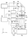
図1は、実施形態における露光装置の構成を示す図である。本明細書および添付図面において、基板であるウエハ115の表面(水平面)をXY平面とするXYZ座標系において方向を示す。XYZ座標系におけるX軸、Y軸、Z軸にそれぞれ平行な方向をX方向、Y方向、Z方向とし、X軸周りの回転、Y軸周りの回転、Z軸周りの回転をそれぞれθX、θY、θZとする。
<First Embodiment>
FIG. 1 is a diagram showing the configuration of an exposure apparatus according to an embodiment. In this specification and the accompanying drawings, directions are shown in an XYZ coordinate system in which the surface (horizontal plane) of the
主制御部103は、後述する露光装置の各部を統括的に制御して露光処理を実行する。主制御部103は、例えば、CPUおよびメモリ(記憶部)を含むコンピュータ装置によって実現されうる。
The
光源100は、複数の波長帯域の光を露光光として出力することができる。光源100より射出された光は、照明光学系104の整形光学系(不図示)を介して所定の形状に整形される。整形された光は、オプティカルインテグレータ(不図示)に入射され、ここで、後述するレチクル109を均一な照度分布で照明するために多数の2次光源が形成される。
The
照明光学系104の開口絞り105の開口部の形状は、ほぼ円形であり、照明光学系制御部108によってその開口部の直径、ひいては照明光学系104の開口数(NA)を所望の値に設定できるようになっている。この場合、投影光学系110の開口数に対する照明光学系104の開口数の比の値がコヒーレンスファクタ(σ値)であるため、照明光学系制御部108は照明光学系104の開口絞り105を制御することで、σ値を設定できる。
The shape of the aperture of the
照明光学系104の光路上にはハーフミラー106が配置され、レチクル109を照明する露光光の一部がこのハーフミラー106により反射されて取り出される。ハーフミラー106の反射光の光路上には紫外光用のフォトセンサ107が配置され、露光光の強度(露光エネルギー)に対応した出力を発生する。原版(マスク)としてのレチクル109には焼き付けを行う半導体デバイスの回路のパターンが形成されており、照明光学系104により照明される。投影光学系110は、レチクル109のパターンを縮小倍率β(例えばβ=1/2)で縮小し、フォトレジストが塗布されたウエハ115上の1つのショット領域を投影するよう配置されている。投影光学系110は、屈折型またはカタディオプトリック系などの光学系でありうる。
A
投影光学系110の瞳面(レチクルに対するフーリエ変換面)上には、開口部がほぼ円形である開口絞り111が配置され、モータ等の開口絞り駆動部112によって開口部の直径を制御することができる。光学素子駆動部113は、フィールドレンズのような、投影光学系110中のレンズ系の一部を構成している光学素子を、投影光学系110の光軸に沿って移動させる。これにより、投影光学系110の諸収差を低減しつつ、投影倍率を良好にさせ歪曲誤差を減らしている。投影光学系制御部114は、主制御部103の制御の下、開口絞り駆動部112及び光学素子駆動部113を制御する。
An
ウエハ115を保持するウエハステージ116(基板ステージ)は、3次元方向に移動可能であり、投影光学系110の光軸方向(Z方向)、及びその方向に直交する面内(X-Y面)を移動できる。なお、上記したとおり、ウエハ115の表面(水平面)をX-Y平面としている。したがって、図1では、Z軸は、投影光学系110の光軸と平行にかつウエハ115からレチクル109に向かう方向に延び、X軸およびY軸は、Z軸と垂直な平面上で互いに直交する方向に延びている。図1において、Y軸は紙面内にあり、X軸は紙面に対して垂直で紙面手前向きである。ウエハステージ116に固定された移動鏡117との間の距離をレーザ干渉計118で計測することでウエハステージ116のX-Y面位置が検出される。また、アライメント計測系124(計測部)を用いて、ウエハ115とウエハステージ116の位置ずれが計測される。露光装置の主制御部103の制御下にあるステージ制御部120は、アライメント計測系124を用いた計測結果に基づいてモータ等のステージ駆動部119を制御することで、ウエハステージ116を所定のX-Y面位置へ移動させる。
A wafer stage 116 (substrate stage) that holds the
投光光学系121および検出光学系122は、フォーカス面を検出する。投光光学系121はウエハ115上のフォトレジストを感光させない非露光光から成る複数個の光束を投光し、その光束はウエハ115上に各々集光されて反射される。ウエハ115で反射された光束は、検出光学系122に入射される。図示は略したが、検出光学系122内には各反射光束に対応させて複数個の位置検出用の受光素子が配置されており、各受光素子の受光面とウエハ115上での各光束の反射点が結像光学系によりほぼ共役となるように構成されている。投影光学系110の光軸方向におけるウエハ115面の位置ずれは、検出光学系122内の位置検出用の受光素子に入射する光の位置ずれとして計測される。
A projection
レチクル109とウエハ115との間の露光光の光路上には、収差補正部材21が配置される。図1の例では、収差補正部材21は、レチクル109と投影光学系110との間に配置されている。収差補正部材21は、投影光学系110とは独立したユニットとして構成されていてもよいし、投影光学系110の一部として構成されていてもよい。収差補正部材21が投影光学系110の内部に設けられる場合、収差補正部材21は、投影光学系110における瞳面より上方で、レチクル109で回折された光をウエハ115上で集光させるフィールドレンズ群の付近に配置されてもよい。あるいは、収差補正部材21は、レチクル109を保持するレチクルホルダまたはレチクルステージ(不図示)と一体的に構成されていてもよい。
An
図2に示すように、収差補正部材21は、第1光学要素211と、露光光の光軸に沿って第1光学要素211とは離間して配置された第2光学要素212とを含む。第1光学要素211および第2光学要素212はそれぞれ、回転非対称な同一の形状の面を間隙の側に有している。第1光学要素211および第2光学要素212のうちの少なくともいずれかは、光学要素駆動部22によってθZ回転(光軸周りの回転)およびZ方向に関する駆動(Z駆動)の少なくともいずれかを行うことができる。更に、第1光学要素211および第2光学要素212のうちの少なくともいずれかは、光学要素駆動部22によって、Z軸と直交するX方向および/またはY方向に移動することができるように構成されていてもよい。
As shown in FIG. 2, the
図2において、第1光学要素211のレチクル109側の外面211aおよび第2光学要素212の投影光学系110側の外面212aはそれぞれ平面形状である。これに対し、第1光学要素211および第2光学要素212の互いに向き合う内側の第1面211bおよび第2面212bは、互いに相補な関係にある非球面形状をなしている。
In FIG. 2, the
図6に、収差補正部材21の駆動の態様を示す。図6(a)は、図2と同様の状態を示している(ただし図6(a)では、第1光学要素211と第2光学要素212との間の隙間の形状は単純化して示されている。)。第1光学要素211および第2光学要素212のうちの少なくともいずれかは、光学要素駆動部22によって、図6(a)の状態から、図6(b)のようにZ駆動されうる。また、第1光学要素211および第2光学要素212のうちの少なくともいずれかは、光学要素駆動部22によって、図6(c)に示されるようにθZ回転されうる。
FIG. 6 shows how the
以下では、第1光学要素211および第2光学要素212のうちの少なくともいずれかのZ駆動およびθZ回転によって収差補正を行うことを説明する。ただし以下では説明を簡単にするため、代表的に第1光学要素211のZ駆動およびθZ回転によって収差補正を行うことを説明する。
In the following, it will be described that aberration correction is performed by Z driving and θZ rotation of at least one of the first
第1面211bおよび第2面212bの回転非対称な形状の面は、例えば次式で表される。ただしAおよびBは定数である。
The rotationally asymmetrical surfaces of the
Z=A(3x2y-y3)+B ・・・(1)
式1で示される回転非対称な形状は、θ=0°の方向(X軸方向)と、
ρ=sqrt(x2+y2)
をパラメータとした極座標表示で表すと、
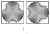
Z=ρ3sin3θ・・・(2)
と等価であり、図5に示すような3回回転対称の非球面形状となる。
Z=A(3x 2 y−y 3 )+B (1)
The rotationally asymmetric shape represented by Equation 1 is in the direction of θ = 0° (X-axis direction),
ρ=sqrt(x 2 +y 2 )
When expressed in polar coordinates with a parameter,
Z=ρ 3 sin3θ (2)
, and has a three-fold rotational symmetry aspherical shape as shown in FIG.
レチクル109上で回折した光束の主光線は物体側テレセントリックであり、第1面211bおよび第2面212bの非球面形状が相補的な作用をする。そのため、第1光学要素211および第2光学要素212を透過したときの各像高間の位相差はゼロになっている。式1で示される非球面形状を持つ第1光学要素211がαだけ回転すると、第1面211bおよび第2面212bの相補性が崩れるが、αが十分小さいとき、位相差は、
Φ≒K*α*R3cos3θ
と表される(ただし、Kは定数)。一方、第1光学素子211が距離dだけZ駆動すると相補性が崩れ、dが十分小さいとき、位相差は、
Φ≒L*d*R3sin3θ
と表される(ただし、Lは定数)。
The principal ray of the light beam diffracted on the
Φ≈K*α*R 3 cos3θ
(where K is a constant). On the other hand, when the first
Φ≈L*d*R 3 sin3θ
(where L is a constant).
このように、第1光学要素211のθZ回転およびZ駆動のどちらでも、3回回転対称成分の位相差が残存する。投影レンズのレチクル対向箇所に3回回転対称の位相差が発生すると、図4に示されるような、台形形状のディストーションが発生することが分かった。第1面211bおよび第2面212bの光軸付近の非球面量は、式2よりほぼ0である。そのため、本実施形態によれば、像高中心は回転やZ駆動による位相変化は起きないため、ディストーションのシフト成分が発生しない。またコマ収差も発生しない。また、光軸から半径Rだけ外れた円周上でも位相の一次の傾き成分は発生しないため、像面の傾きも発生しない。よって、特許文献2(特開2014-120682号公報)に開示されるような、光学偏心によって台形形状を生成する場合よりも、像高間で発生するアスは抑えられ、有効である。
Thus, the phase difference of the 3-fold rotational symmetry component remains in both the θZ rotation and the Z drive of the first
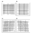
光学要素駆動部22により第1光学要素211をθZ回転させることにより、図4(a),(b)に示されるような、左右の辺(Y方向に沿う2つの辺)が上底、下底をなす台形形状のディストーションが発生する。また、光学要素駆動部22により第1光学要素211をZ駆動することにより、図4(c),(d)に示されるような、上下の辺(X方向に沿う2つの辺))が上底、下底をなす台形形状のディストーションが発生する。台形の上底および下底をなす2本の対辺の長さの差をΔbaseとすると、θZ回転の回転方向、Z駆動の駆動方向により、Δbaseの符号が反転し、Δbaseの値は、θZ回転の回転角、Z駆動の駆動量によって一意に決まる。したがって、第1光学要素211のθZ回転の回転角、Z駆動の駆動量を調整することによって、図9のような、左右の辺の長さが異なる台形Δbase_LR、上下の辺の長さが異なる台形Δbase_UDを含む任意の台形形状をそれぞれ補正することができる。
By rotating the first
図7のフローチャートを参照して、実施形態における露光方法の一例を説明する。ウエハがロードされた後、S1で主制御部103は、アライメント計測系124を用いて、下地となる複数のショット領域のそれぞれの形状を計測し、各ショット領域の歪みのデータを記憶部に記憶する。この計測は、露光装置外の計測装置で行われてもよく、その場合には、主制御部103は、外部から各ショット領域の歪みのデータを取得する。
An example of the exposure method in the embodiment will be described with reference to the flowchart of FIG. After the wafer is loaded, in S1, the
S2で主制御部103は、各ショット領域の形状に合わせて露光するために、収差の2方向の成分(Δbase_LR成分、Δbase_UD成分)の調整すべき量(調整量)を計算する。
In S2, the
S3で光学要素制御部123は、光学要素駆動部22を制御して、Δbase_LR成分とΔbase_UD成分とを調整するよう第1光学要素211のθZ回転およびZ駆動の少なくともいずれかを行う。このとき、他の像ずれ成分をも調整するために、投影光学系制御部114は、光学素子駆動部113を制御して、投影光学系110の光学素子を駆動してもよい。同様に、他の像ずれ成分をも調整するために、ステージ制御部120は、ステージ駆動部119を制御して、ウエハステージ116を駆動してもよい。
In S3, the optical
第1光学要素211の駆動が完了したら、S4で主制御部103は、露光を行う。S5で主制御部103は、ステージ制御部120を介してステージ駆動部119を制御して、次の露光すべきショット領域に移動するようにウエハステージ116を駆動する。主制御部103は、S1で得られた歪みのデータおよびS2で計算された調整量に基づき、第1光学要素211の駆動と露光とを繰り返す。 S6において全ショット領域の露光が終了したら、主制御部103は、ウエハをアンロードし、次のウエハをロードして上記のフローを繰り返し行う。
After the driving of the first
このフローに基づいた露光方法によれば、左右の辺の長さが異なる台形形状成分を有する下地のショット形状、または、上下の辺の長さが異なる台形形状成分を有する下地のショット形状に合わせた調整を施して露光することができる。これにより重ね合わせ精度が向上する。 According to the exposure method based on this flow, it is possible to match the shot shape of the background having trapezoidal components with different left and right side lengths, or the shot shape of the background having trapezoidal components with different upper and lower side lengths. can be adjusted and exposed. This improves the overlay accuracy.
上述の例では、式1で示される回転非対称な形状を持つ第1光学要素211のθZ回転やZ駆動により台形形状を補正する例を示した。ここで、特開2014-120682号公報(特許文献2)に開示されている技術を用いると、光学要素駆動部22により第1光学要素211をX軸方向に沿って駆動することにより、図3(c)、(d)に示すTY_45成分のディストーションが発生する。また、第1光学要素211をY軸方向に沿って駆動することにより、図3(a)、(b)に示すTY_0成分のディストーションが発生する。よって、第1光学要素211をX方向、Y方向、Z方向、θZ回転方向の駆動量を同時に制御することで台形成分と縦横倍率差成分の両方を制御することができる。
In the above example, an example of correcting the trapezoidal shape by θZ rotation or Z driving of the first
図8(a)に一般的なウエハ内の露光順序の例を示す。各格子はショットを表し、格子間の矢印は、一つ前の露光ショットからのステージ移動方向を示している。図8(a)の場合、紙面左右方向(X方向)の隣接ショットからのステップ駆動の頻度が高い。一つ前に露光されたショットがウエハに与える熱量によって、ウエハの熱膨張が発生する。ここで、ショットから遠ざかるほど熱膨張量は減る。そうすると、X方向へのステップ駆動を伴う順次露光においては、左右方向に熱膨張量が変わるため、ショット領域は左右方向に台形の辺の長さが異なるようなディストーション形状となる。この場合、Δbase_LRの調整量が有効的になる。 FIG. 8A shows an example of a general exposure order within a wafer. Each grid represents a shot, and the arrow between grids indicates the direction of stage movement from the previous exposure shot. In the case of FIG. 8A, the frequency of step driving from adjacent shots in the lateral direction (X direction) of the paper surface is high. Thermal expansion of the wafer occurs due to the amount of heat that the previously exposed shot imparts to the wafer. Here, the amount of thermal expansion decreases as the distance from the shot increases. Then, in sequential exposure accompanied by step driving in the X direction, the amount of thermal expansion changes in the horizontal direction, so the shot area has a distorted shape in which the side lengths of the trapezoid are different in the horizontal direction. In this case, the adjustment amount of Δbase_LR becomes effective.
Δbase_LRの調整は、第1光学要素211および第2光学要素212の互いに向き合う内側の第1面211bおよび第2面212bの3回回転対称の非球面形状と関係する。これら内側の面211bおよび212bを式1で表されるようなsin3θの位相を持つ非球面形状とすることにより、相補的な光学素子の回転駆動によってΔbase_LRを発生させることができる。一般に、回転駆動の方がZ駆動に比べて高速に動かすことができるため、図8(a)のショット露光順序の際にはsinθの位相を持つ非球面が望ましい。TY_0成分およびTY_45成分(特開2014-120682号公報(特許文献2)参照。)の調整はそれぞれ、光学要素のX方向およびY方向への駆動によって実現され、いずれも光学要素の水平方向の駆動であるため、同一平面上のシフトと回転の駆動を単純な機構で構成可能である。
The adjustment of Δbase_LR is related to the three-fold rotationally symmetrical aspheric shapes of the inner first and
本実施形態において、第1光学要素211は、露光光の光軸に関して3回回転対称な非球面形状を持つ第1面211bを有する。また、第2光学要素212は、第1面211bと対向し、第1光学要素211で発生する収差を相補的に補正する非球面形状を持つ第2面212bを有する。
In this embodiment, the first
第1光学要素211および第2光学要素212の互いに向き合う第1面211bおよび第2面212bの回転非対称な形状は、例えば次式で表される形にしてもよい。ただし、C、Dは定数である。
The rotationally asymmetric shape of the
Z=C(x3-3xy2)+D ・・・(3) Z=C(x 3 −3xy 2 )+D (3)
式3を極座標表示で表すと、次式のようになる。 Representing Equation 3 in polar coordinates gives the following equation.
Z=ρ3cos3θ・・・(4) Z=ρ 3 cos 3θ (4)
第1光学要素211の回転量により上下の辺の長さが異なる台形Δbase_UDのディストーションが発生し、第1光学要素211のZ駆動の駆動量により左右の辺の長さが異なる台形Δbase_LRのディストーションが発生する。また、第1光学要素211をY方向に駆動することにより、図3の(c)、(d)に示すTY_45成分のディストーションが発生する。さらに、第1光学要素211をX方向に駆動することにより、図3の(a)、(b)に示すTY_0成分のディストーションが発生する。
The amount of rotation of the first
ウエハ内の露光順序を図8(b)のようにする場合には、紙面上下方向(Y方向)の隣接ショットからのステップ駆動の頻度が高い。Y方向の駆動では図8(b)の紙面上下方向に膨張が変わるため、ショット領域は紙面上下方向に台形の辺の長さが異なるようなディストーション形状となる。この場合、Δbase_UDの調整量が有効的になる。 When the exposure order within the wafer is as shown in FIG. 8B, the frequency of step driving from adjacent shots in the vertical direction (Y direction) of the paper surface is high. When driving in the Y direction, the expansion changes in the vertical direction of the paper surface of FIG. In this case, the adjustment amount of Δbase_UD becomes effective.
Δbase_UDの調整は、第1光学要素211および第2光学要素212の互いに向き合う第1面211bおよび第2面212bの3回回転対称の非球面形状と関係する。これら第1面211bおよび第2面212bを式3で表されるようなcos3θの位相を持つ非球面形状とすることにより、相補的な光学素子の回転駆動によってΔbase_UDを発生させることができる。図8(b)のショット露光順序の際にはcosθの位相を持つ非球面が望ましい。
The adjustment of Δbase_UD is related to the three-fold rotationally symmetrical aspheric shapes of the mutually facing first and
露光装置は、生産効率の観点から、一般にショット領域の露光順序に規則性がある。上記のように、第1光学要素211および第2光学要素212の互いに向き合う第1面211bおよび第2面212bを、ウエハ内のショット領域の露光順序に応じた非球面形状とすることにより、単純な駆動機構の構成で重ね合せ精度を向上させることができる。
From the viewpoint of production efficiency, an exposure apparatus generally has regularity in the exposure order of shot areas. As described above, the
第1光学要素211および第2光学要素212の互いに向き合う第1面211bおよび第2面212bの非球面形状については、式1および式3の例を挙げたが、これに限定されない。例えば、次の式5、式6のように表される3回回転対称の非球面形状であっても、同様の効果が得られる。ただし、f(ρ)、g(ρ)はρを変数とする関数、E、Fは定数である。
As for the aspheric shapes of the
Z=f(ρ)cos3θ+E・・・(5)、
Z=g(ρ)sin3θ+F・・・(6)
このように、3回回転対称の非球面を持つ光学要素の回転およびZ駆動の少なくともいずれかにより、効果的に下地の台形形状のディストーションを補正することができる。
Z=f(ρ)cos3θ+E (5),
Z=g(ρ) sin3θ+F (6)
Thus, the trapezoidal distortion of the base can be effectively corrected by at least one of rotation and Z-drive of the optical element having the aspherical surface with 3-fold rotational symmetry.
<第2実施形態>
次に、図10を参照して、台形形状を持つ歪曲収差を調整する収差補正部材21を用いた露光方法の別の例について説明する。S11で、主制御部103は、露光前に、前のショットの露光光によるウエハ変形の影響度の情報を取得する。露光光によるウエハ変形の影響度は、例えば、露光エネルギーによる入熱パラメータと、前ショットからのステージ移動ベクトルに関するパラメータと、ウエハの物性に関するパラメータ等の露光条件に基づいて決定される。
<Second embodiment>
Next, another example of the exposure method using the
ウエハの物性に関するパラメータは、線膨張係数および熱伝導率を含みうる。線膨張係数により、熱によるウエハの伸縮係数が決定される。また、前のショット領域の中心と次に露光するショット領域の両端とに距離の差が存在するため、ウエハの熱伝導率に相応する、ショット領域の両端の膨張率の差が発生する。ウエハには、例えば、Si、GaAs、あるいはガラス基板など、物性が異なる基板が使われうる。また、ウエハには、下地処理プロセスによってCu層が構成されることもある。これらのことから、ウエハの物性に変化が生じうる。 Parameters related to wafer physical properties may include linear expansion coefficient and thermal conductivity. The coefficient of linear expansion determines the expansion coefficient of the wafer due to heat. In addition, since there is a difference in distance between the center of the previous shot area and both ends of the next shot area to be exposed, there occurs a difference in expansion coefficient between both ends of the shot area corresponding to the thermal conductivity of the wafer. Substrates having different physical properties, such as Si, GaAs, or glass substrates, may be used as the wafer. The wafer may also be provided with a Cu layer by a priming process. For these reasons, the physical properties of the wafer may change.
露光エネルギーによる入熱パラメータは、露光量、ウエハの露光光反射率、透過率を含みうる。ウエハ上に塗布されている感光剤は、その種類に応じた適正露光量が決まっている。ショット領域のサイズと露光量との積によって照射エネルギーが求まり、このうち、基板の反射光、透過光を除いたエネルギーがウエハの熱変形に寄与する吸収エネルギーである。ウエハには、この吸収エネルギーに比例した熱変形が発生する。 Heat input parameters due to exposure energy may include exposure dose, wafer exposure light reflectance, and transmittance. The appropriate amount of exposure is determined according to the type of photosensitive agent applied on the wafer. The irradiation energy is obtained from the product of the size of the shot area and the exposure amount, and the energy excluding the reflected light and transmitted light of the substrate is the absorbed energy that contributes to the thermal deformation of the wafer. The wafer undergoes thermal deformation proportional to this absorbed energy.
ステージ移動ベクトルに関するパラメータは、ショット間ピッチと複数のショット領域の露光順序の情報を含む。 Parameters related to the stage movement vector include information on the shot-to-shot pitch and the exposure order of the multiple shot areas.
ウエハ上の各ショット間のピッチは、逐次的に露光する露光装置のショット領域間の基板ステージの駆動時間に関係する。したがって、ウエハ上の各ショット間のピッチによって、前ショットの露光完了後から対象ショットの露光開始までの時間が決定される。ショットの露光順序によって、前ショットの中心と露光ショットとの位置関係が決まり、露光ショットに伝達する熱の分布が求まるため、ショット端部の基板の膨張率の差が決定される。これは台形形状の向きを表す。 The pitch between shots on the wafer is related to the driving time of the substrate stage between shot areas of the exposure apparatus that are sequentially exposed. Therefore, the pitch between shots on the wafer determines the time from the completion of exposure of the previous shot to the start of exposure of the target shot. The order of exposure of the shots determines the positional relationship between the center of the previous shot and the exposure shots, and the distribution of heat transmitted to the exposure shots is determined. This represents the orientation of the trapezoidal shape.
また、複数のウエハへ連続的に露光していく場合には、ウエハステージの蓄熱量も重要なパラメータになる。ウエハステージの温度が上昇することにより、ウエハ搭載後のウエハの熱変形が発生するためである。 Further, when continuously exposing a plurality of wafers, the amount of heat stored in the wafer stage is also an important parameter. This is because the temperature rise of the wafer stage causes thermal deformation of the wafer after the wafer is mounted.
例えば、主制御部103は、複数の条件で実際に露光を行い、その結果として現れたディストーションを計測することにより、条件毎のウエハ変形の影響度を求め、これをデータベース(テーブル)として記憶部に記憶しておく。主制御部103は、S11では、このテーブルを参照して影響度を取得してもよい。あるいは、条件毎のウエハ変形の影響度を関数化しておき、主制御部103は、露光時の条件をその関数に当てはめることにより影響度を算出してもよい。
For example, the
このように、前ショットの露光熱がウエハ変形に与える影響を決定するパラメータ(条件)を取得することにより、発生する台形成分を予測することができる。 In this way, by acquiring the parameters (conditions) that determine the influence of the exposure heat of the previous shot on the wafer deformation, it is possible to predict the generated trapezoidal component.
次に、S12で、主制御部103は、S11で取得した影響度に基づいて、台形成分の発生量を予測する。主制御部103は、予測された台形成分の発生量に基づいて、光学要素制御部123により台形成分を補正するために必要な光学要素の駆動量を算出する。S13で、主制御部103は、光学要素駆動部22を制御して、S12で算出された駆動量で、第1光学要素211のθZ回転およびZ駆動の少なくともいずれかを行う。以上の収差補正が行われた後、S14で、主制御部103は露光を行う。
Next, in S12, the
上記した露光方法によれば、ウエハの物性や露光装置の露光量、ステージ駆動速度等に応じて、露光光の熱によるウエハの変形量が変化する場合にも、ディストーションの台形成分を良好に補正して露光を行うことができる。 According to the exposure method described above, even when the amount of deformation of the wafer due to the heat of the exposure light changes according to the physical properties of the wafer, the exposure amount of the exposure apparatus, the stage driving speed, etc., the table-forming portion of distortion can be satisfactorily controlled. Exposure can be performed with correction.
なお、上述の実施形態では、台形成分を補正する例を示したが、補正対象は台形成分に限定されない。 In the above-described embodiment, an example of correcting the trapezoidal component was shown, but the correction target is not limited to the trapezoidal component.
また、上述の実施形態では、例えば式1の形状を持つ第1光学要素211のX方向の駆動によってTY_0成分を、Y方向の駆動によってTY_45成分を調整できることを示した。したがって、θZ回転、Z駆動、Z方向の駆動、Y方向の駆動を組み合わせることにより、任意の方向の縦横倍率差成分の調整および台形形状の補正を行うが可能となる。
Further, in the above embodiment, it was shown that the TY_0 component can be adjusted by driving the first
上記のとおり、ウエハ上の大部分のショット領域に必要なΔbase_LRの調整は、θZ回転により行われる。また、TY_0成分およびTY_45成分はそれぞれ、X方向の駆動およびY方向の駆動により行われる。いずれも第1光学要素211の水平方向の駆動であるため、単純な駆動機構の構成で補正が実現される。
As noted above, the adjustment of Δbase_LR required for most shot areas on the wafer is done by the θZ rotation. Also, the TY_0 component and the TY_45 component are performed by driving in the X direction and driving in the Y direction, respectively. In both cases, since the first
このように、実施形態によれば、収差補正部材は、3回回転対称の非球面を持つ光学要素のθZ回転の機構およびZ駆動の機構の少なくともいずれかを有する。これにより、前のショットの露光光による基板変形の影響度を取得して、効果的に台形形状のディストーションを補正することができる。 Thus, according to the embodiment, the aberration correction member has at least one of a θZ rotation mechanism and a Z drive mechanism of an optical element having an aspherical surface with three-fold rotational symmetry. This makes it possible to obtain the degree of influence of the substrate deformation due to the exposure light of the previous shot and effectively correct the trapezoidal distortion.
なお、本発明は、下地のディストーションを計測して台形成分を下地に合わせて補正することに限定されない。第1レイヤーのディストーションの台形成分を補正して、格子等の所望の形状に近づけるディストーションにしておき、第2レイヤー以降で露光する際の重ね合せ精度を向上させることもできる。 It should be noted that the present invention is not limited to measuring the distortion of the background and correcting the trapezoidal component in accordance with the background. It is also possible to correct the trapezoidal component of the distortion of the first layer and set the distortion close to a desired shape such as a grid, thereby improving the overlay accuracy when exposing the second layer and thereafter.
<物品製造方法の実施形態>
本発明の実施形態に係る物品製造方法は、例えば、半導体デバイス等のマイクロデバイスや微細構造を有する素子等の物品を製造するのに好適である。本実施形態の物品製造方法は、基板に塗布された感光剤に上記の露光装置を用いて潜像パターンを形成する工程(基板を露光する工程)と、かかる工程で潜像パターンが形成された基板を現像する工程とを含む。更に、かかる製造方法は、他の周知の工程(酸化、成膜、蒸着、ドーピング、平坦化、エッチング、レジスト剥離、ダイシング、ボンディング、パッケージング等)を含む。本実施形態の物品製造方法は、従来の方法に比べて、物品の性能・品質・生産性・生産コストの少なくとも1つにおいて有利である。
<Embodiment of article manufacturing method>
INDUSTRIAL APPLICABILITY The article manufacturing method according to the embodiment of the present invention is suitable for manufacturing articles such as microdevices such as semiconductor devices and elements having fine structures. The method for manufacturing an article according to the present embodiment includes a step of forming a latent image pattern on a photosensitive agent applied to a substrate using the above exposure apparatus (a step of exposing the substrate), and and developing the substrate. In addition, such manufacturing methods include other well-known steps (oxidation, deposition, deposition, doping, planarization, etching, resist stripping, dicing, bonding, packaging, etc.). The article manufacturing method of the present embodiment is advantageous in at least one of article performance, quality, productivity, and production cost compared to conventional methods.
<他の実施形態>
本発明は、上述の実施形態の1以上の機能を実現するプログラムを、ネットワーク又は記憶媒体を介してシステム又は装置に供給し、そのシステム又は装置のコンピュータにおける1つ以上のプロセッサがプログラムを読み出し実行する処理でも実現可能である。また、1以上の機能を実現する回路(例えば、ASIC)によっても実現可能である。
<Other embodiments>
The present invention supplies a program that implements one or more functions of the above-described embodiments to a system or apparatus via a network or a storage medium, and one or more processors in the computer of the system or apparatus reads and executes the program. It can also be realized by processing to It can also be implemented by a circuit (for example, ASIC) that implements one or more functions.
発明は上記実施形態に制限されるものではなく、発明の精神及び範囲から離脱することなく、様々な変更及び変形が可能である。従って、発明の範囲を公にするために請求項を添付する。 The invention is not limited to the embodiments described above, and various modifications and variations are possible without departing from the spirit and scope of the invention. Accordingly, the claims are appended to make public the scope of the invention.
21:収差補正部材、100:光源、103:主制御部、104:照明光学系、110:投影光学系、116:ウエハステージ 21: aberration correction member, 100: light source, 103: main controller, 104: illumination optical system, 110: projection optical system, 116: wafer stage
Claims (14)
前記原版と前記基板との間の露光光の光路上に配置された収差補正部材と、
前記収差補正部材を駆動する駆動部と、を有し、
前記収差補正部材は、
3回回転対称な非球面形状を持つ第1面を有する第1光学要素と、
前記投影光学系の光軸に沿って前記第1光学要素とは離間して配置された第2光学要素であって、前記第1面と対向し、前記第1面が有する前記非球面形状と相補的な関係にある非球面形状を有する第2面を有する第2光学要素と、を含み、
前記駆動部は、前記ショット領域の形状の台形成分に基づいて、前記第1光学要素および前記第2光学要素の少なくとも1つの、前記光軸周りの回転および前記光軸に沿う駆動の少なくともいずれかを行う
ことを特徴とする露光装置。 An exposure apparatus for exposing a substrate by projecting a pattern of an original onto a shot area of the substrate via a projection optical system,
an aberration correction member arranged on an optical path of exposure light between the original and the substrate;
a driving unit that drives the aberration correction member;
The aberration correction member is
a first optical element having a first surface with a three -fold rotational symmetry aspherical shape;
a second optical element spaced apart from the first optical element along the optical axis of the projection optical system, facing the first surface and having the aspheric shape of the first surface; a second optical element having a second surface with a complementary aspherical shape ;
The driving unit rotates at least one of the first optical element and the second optical element based on a trapezoidal component of the shape of the shot area, and drives at least one of the rotation about the optical axis and the driving along the optical axis. An exposure apparatus characterized by:
前記制御部は、前記計測部から前記ショット領域の形状のデータを取得することを特徴とする請求項8に記載の露光装置。 further comprising a measurement unit that measures the shape of the shot area;
9. An exposure apparatus according to claim 8, wherein said control unit acquires shape data of said shot area from said measurement unit.
前記露光された基板を現像する工程と、
を含み、前記現像された基板から物品を製造することを特徴とする物品製造方法。 exposing a substrate using the exposure apparatus according to any one of claims 1 to 13;
developing the exposed substrate;
and manufacturing an article from the developed substrate.
Priority Applications (7)
| Application Number | Priority Date | Filing Date | Title |
|---|---|---|---|
| JP2019045138A JP7178932B2 (en) | 2019-03-12 | 2019-03-12 | Exposure apparatus and article manufacturing method |
| EP20159086.6A EP3709083A1 (en) | 2019-03-12 | 2020-02-24 | Exposure apparatus and article manufacturing method |
| TW109105960A TWI772756B (en) | 2019-03-12 | 2020-02-25 | Exposure apparatus and article manufacturing method |
| US16/809,097 US11061337B2 (en) | 2019-03-12 | 2020-03-04 | Exposure apparatus and article manufacturing method |
| KR1020200029382A KR20200109261A (en) | 2019-03-12 | 2020-03-10 | Exposure apparatus and article manufacturing method |
| SG10202002243WA SG10202002243WA (en) | 2019-03-12 | 2020-03-11 | Exposure apparatus and article manufacturing method |
| CN202010179074.1A CN111694225B (en) | 2019-03-12 | 2020-03-12 | Exposure apparatus and article manufacturing method |
Applications Claiming Priority (1)
| Application Number | Priority Date | Filing Date | Title |
|---|---|---|---|
| JP2019045138A JP7178932B2 (en) | 2019-03-12 | 2019-03-12 | Exposure apparatus and article manufacturing method |
Publications (3)
| Publication Number | Publication Date |
|---|---|
| JP2020148865A JP2020148865A (en) | 2020-09-17 |
| JP2020148865A5 JP2020148865A5 (en) | 2022-03-17 |
| JP7178932B2 true JP7178932B2 (en) | 2022-11-28 |
Family
ID=69726501
Family Applications (1)
| Application Number | Title | Priority Date | Filing Date |
|---|---|---|---|
| JP2019045138A Active JP7178932B2 (en) | 2019-03-12 | 2019-03-12 | Exposure apparatus and article manufacturing method |
Country Status (7)
| Country | Link |
|---|---|
| US (1) | US11061337B2 (en) |
| EP (1) | EP3709083A1 (en) |
| JP (1) | JP7178932B2 (en) |
| KR (1) | KR20200109261A (en) |
| CN (1) | CN111694225B (en) |
| SG (1) | SG10202002243WA (en) |
| TW (1) | TWI772756B (en) |
Citations (4)
| Publication number | Priority date | Publication date | Assignee | Title |
|---|---|---|---|---|
| JP2008028388A (en) | 2006-07-18 | 2008-02-07 | Asml Netherlands Bv | Lithography equipment, aberration correction device, and device fabrication method |
| JP2010266687A (en) | 2009-05-14 | 2010-11-25 | Nikon Corp | Exposure method, exposure apparatus and device producing method |
| JP2014120682A (en) | 2012-12-18 | 2014-06-30 | Canon Inc | Exposure device, exposure method and method of manufacturing device |
| JP2014168031A (en) | 2013-01-30 | 2014-09-11 | Canon Inc | Lithography apparatus, lithography method, and method of manufacturing article |
Family Cites Families (16)
| Publication number | Priority date | Publication date | Assignee | Title |
|---|---|---|---|---|
| JP3064432B2 (en) | 1990-12-26 | 2000-07-12 | 株式会社ニコン | Projection exposure apparatus, projection exposure method, and circuit manufacturing method |
| JPH0982601A (en) * | 1995-09-12 | 1997-03-28 | Nikon Corp | Projection aligner |
| JPH10142555A (en) * | 1996-11-06 | 1998-05-29 | Nikon Corp | Projection exposure device |
| EP1037266A4 (en) * | 1997-10-07 | 2002-09-11 | Nikon Corp | Projection exposure method and apparatus |
| JP3179406B2 (en) * | 1998-02-26 | 2001-06-25 | 日本電気ファクトリエンジニアリング株式会社 | Exposure method and apparatus |
| JP3031375B2 (en) | 1998-04-23 | 2000-04-10 | キヤノン株式会社 | Lens barrel and projection exposure apparatus using the same |
| JP3459773B2 (en) * | 1998-06-24 | 2003-10-27 | キヤノン株式会社 | Projection exposure apparatus and device manufacturing method |
| JP2002175964A (en) * | 2000-12-06 | 2002-06-21 | Nikon Corp | Observation system and method of manufacturing the same, aligner, and method of manufacturing microdevice |
| JP3358192B2 (en) * | 2001-05-31 | 2002-12-16 | 株式会社ニコン | Projection exposure apparatus, exposure method, semiconductor manufacturing method, and projection optical system adjustment method |
| WO2006064728A1 (en) * | 2004-12-16 | 2006-06-22 | Nikon Corporation | Projection optical system, exposure apparatus, exposure system, and exposure method |
| EP1953805A4 (en) * | 2005-11-10 | 2010-03-31 | Nikon Corp | Lighting optical system, exposure system, and exposure method |
| JP5406437B2 (en) * | 2007-06-22 | 2014-02-05 | キヤノン株式会社 | Exposure apparatus and device manufacturing method |
| DE102008001892A1 (en) * | 2008-05-21 | 2009-11-26 | Carl Zeiss Smt Ag | Optical system for microlithography |
| EP2219077A1 (en) * | 2009-02-12 | 2010-08-18 | Carl Zeiss SMT AG | Projection exposure method, projection exposure system and projection objective |
| JP2015204312A (en) * | 2014-04-10 | 2015-11-16 | キヤノン株式会社 | Projection optical system, exposure device, and manufacturing method of article |
| DE102015218329A1 (en) * | 2015-09-24 | 2017-03-30 | Carl Zeiss Smt Gmbh | Optical correction arrangement, projection objective with such an optical correction arrangement as well as a microlithographic apparatus with such a projection objective |
-
2019
- 2019-03-12 JP JP2019045138A patent/JP7178932B2/en active Active
-
2020
- 2020-02-24 EP EP20159086.6A patent/EP3709083A1/en active Pending
- 2020-02-25 TW TW109105960A patent/TWI772756B/en active
- 2020-03-04 US US16/809,097 patent/US11061337B2/en active Active
- 2020-03-10 KR KR1020200029382A patent/KR20200109261A/en not_active Application Discontinuation
- 2020-03-11 SG SG10202002243WA patent/SG10202002243WA/en unknown
- 2020-03-12 CN CN202010179074.1A patent/CN111694225B/en active Active
Patent Citations (4)
| Publication number | Priority date | Publication date | Assignee | Title |
|---|---|---|---|---|
| JP2008028388A (en) | 2006-07-18 | 2008-02-07 | Asml Netherlands Bv | Lithography equipment, aberration correction device, and device fabrication method |
| JP2010266687A (en) | 2009-05-14 | 2010-11-25 | Nikon Corp | Exposure method, exposure apparatus and device producing method |
| JP2014120682A (en) | 2012-12-18 | 2014-06-30 | Canon Inc | Exposure device, exposure method and method of manufacturing device |
| JP2014168031A (en) | 2013-01-30 | 2014-09-11 | Canon Inc | Lithography apparatus, lithography method, and method of manufacturing article |
Also Published As
| Publication number | Publication date |
|---|---|
| CN111694225A (en) | 2020-09-22 |
| CN111694225B (en) | 2023-11-21 |
| TW202036176A (en) | 2020-10-01 |
| JP2020148865A (en) | 2020-09-17 |
| TWI772756B (en) | 2022-08-01 |
| EP3709083A1 (en) | 2020-09-16 |
| US20200292945A1 (en) | 2020-09-17 |
| KR20200109261A (en) | 2020-09-22 |
| US11061337B2 (en) | 2021-07-13 |
| SG10202002243WA (en) | 2020-10-29 |
Similar Documents
| Publication | Publication Date | Title |
|---|---|---|
| TWI641959B (en) | Process window identifier | |
| JP3303758B2 (en) | Projection exposure apparatus and device manufacturing method | |
| JP2008171960A (en) | Position detection device and exposure device | |
| JP7147738B2 (en) | Measuring device, measuring method, and exposure device | |
| JP6463935B2 (en) | Exposure apparatus, exposure method, and device manufacturing method | |
| WO1999005709A1 (en) | Exposure method and aligner | |
| JP6882091B2 (en) | Exposure equipment and manufacturing method of articles | |
| US20060227334A1 (en) | Aberration measuring method for projection optical system with a variable numerical aperture in an exposure apparatus | |
| JP2002170754A (en) | Exposure system, method of detecting optical characteristic, and exposure method | |
| JPWO2002025711A1 (en) | Measurement method of exposure characteristics and exposure method | |
| JP6806509B2 (en) | Method of manufacturing exposure equipment and articles | |
| JP6015930B2 (en) | Exposure method, exposure apparatus, and device manufacturing method | |
| JP2897345B2 (en) | Projection exposure equipment | |
| KR102372650B1 (en) | Projection optical system, exposure apparatus, method of manufacturing article, and adjusting method | |
| JP7178932B2 (en) | Exposure apparatus and article manufacturing method | |
| JP2010123755A (en) | Exposure apparatus, and device manufacturing method | |
| JP2020071274A (en) | Exposure apparatus and method for manufacturing article | |
| JP3958261B2 (en) | Optical system adjustment method | |
| JP7022531B2 (en) | Exposure method, exposure equipment, and manufacturing method of goods | |
| JP6139870B2 (en) | Exposure method, exposure apparatus, and article manufacturing method | |
| JP5414288B2 (en) | Exposure method and apparatus, and device manufacturing method | |
| JP2014120682A (en) | Exposure device, exposure method and method of manufacturing device | |
| JP6448220B2 (en) | Exposure apparatus, exposure method, and device manufacturing method | |
| JP6226525B2 (en) | Exposure apparatus, exposure method, and device manufacturing method using them | |
| JP5445905B2 (en) | Alignment method and apparatus, and exposure method and apparatus |
Legal Events
| Date | Code | Title | Description |
|---|---|---|---|
| RD01 | Notification of change of attorney |
Free format text: JAPANESE INTERMEDIATE CODE: A7421 Effective date: 20210103 |
|
| A521 | Request for written amendment filed |
Free format text: JAPANESE INTERMEDIATE CODE: A523 Effective date: 20210113 |
|
| A521 | Request for written amendment filed |
Free format text: JAPANESE INTERMEDIATE CODE: A523 Effective date: 20220308 |
|
| A621 | Written request for application examination |
Free format text: JAPANESE INTERMEDIATE CODE: A621 Effective date: 20220308 |
|
| A977 | Report on retrieval |
Free format text: JAPANESE INTERMEDIATE CODE: A971007 Effective date: 20221007 |
|
| TRDD | Decision of grant or rejection written | ||
| A01 | Written decision to grant a patent or to grant a registration (utility model) |
Free format text: JAPANESE INTERMEDIATE CODE: A01 Effective date: 20221017 |
|
| A61 | First payment of annual fees (during grant procedure) |
Free format text: JAPANESE INTERMEDIATE CODE: A61 Effective date: 20221115 |
|
| R151 | Written notification of patent or utility model registration |
Ref document number: 7178932 Country of ref document: JP Free format text: JAPANESE INTERMEDIATE CODE: R151 |