JP7169171B2 - Semiconductor device and distance measuring device - Google Patents
Semiconductor device and distance measuring device Download PDFInfo
- Publication number
- JP7169171B2 JP7169171B2 JP2018216715A JP2018216715A JP7169171B2 JP 7169171 B2 JP7169171 B2 JP 7169171B2 JP 2018216715 A JP2018216715 A JP 2018216715A JP 2018216715 A JP2018216715 A JP 2018216715A JP 7169171 B2 JP7169171 B2 JP 7169171B2
- Authority
- JP
- Japan
- Prior art keywords
- signal
- phase
- input signal
- digital signal
- semiconductor device
- Prior art date
- Legal status (The legal status is an assumption and is not a legal conclusion. Google has not performed a legal analysis and makes no representation as to the accuracy of the status listed.)
- Active
Links
Images


Classifications
-
- G—PHYSICS
- G01—MEASURING; TESTING
- G01S—RADIO DIRECTION-FINDING; RADIO NAVIGATION; DETERMINING DISTANCE OR VELOCITY BY USE OF RADIO WAVES; LOCATING OR PRESENCE-DETECTING BY USE OF THE REFLECTION OR RERADIATION OF RADIO WAVES; ANALOGOUS ARRANGEMENTS USING OTHER WAVES
- G01S7/00—Details of systems according to groups G01S13/00, G01S15/00, G01S17/00
- G01S7/48—Details of systems according to groups G01S13/00, G01S15/00, G01S17/00 of systems according to group G01S17/00
- G01S7/483—Details of pulse systems
- G01S7/486—Receivers
- G01S7/4861—Circuits for detection, sampling, integration or read-out
-
- G—PHYSICS
- G01—MEASURING; TESTING
- G01S—RADIO DIRECTION-FINDING; RADIO NAVIGATION; DETERMINING DISTANCE OR VELOCITY BY USE OF RADIO WAVES; LOCATING OR PRESENCE-DETECTING BY USE OF THE REFLECTION OR RERADIATION OF RADIO WAVES; ANALOGOUS ARRANGEMENTS USING OTHER WAVES
- G01S17/00—Systems using the reflection or reradiation of electromagnetic waves other than radio waves, e.g. lidar systems
- G01S17/02—Systems using the reflection of electromagnetic waves other than radio waves
- G01S17/06—Systems determining position data of a target
- G01S17/08—Systems determining position data of a target for measuring distance only
- G01S17/10—Systems determining position data of a target for measuring distance only using transmission of interrupted, pulse-modulated waves
- G01S17/26—Systems determining position data of a target for measuring distance only using transmission of interrupted, pulse-modulated waves wherein the transmitted pulses use a frequency-modulated or phase-modulated carrier wave, e.g. for pulse compression of received signals
-
- G—PHYSICS
- G01—MEASURING; TESTING
- G01S—RADIO DIRECTION-FINDING; RADIO NAVIGATION; DETERMINING DISTANCE OR VELOCITY BY USE OF RADIO WAVES; LOCATING OR PRESENCE-DETECTING BY USE OF THE REFLECTION OR RERADIATION OF RADIO WAVES; ANALOGOUS ARRANGEMENTS USING OTHER WAVES
- G01S17/00—Systems using the reflection or reradiation of electromagnetic waves other than radio waves, e.g. lidar systems
- G01S17/02—Systems using the reflection of electromagnetic waves other than radio waves
- G01S17/06—Systems determining position data of a target
- G01S17/08—Systems determining position data of a target for measuring distance only
- G01S17/10—Systems determining position data of a target for measuring distance only using transmission of interrupted, pulse-modulated waves
- G01S17/14—Systems determining position data of a target for measuring distance only using transmission of interrupted, pulse-modulated waves wherein a voltage or current pulse is initiated and terminated in accordance with the pulse transmission and echo reception respectively, e.g. using counters
-
- G—PHYSICS
- G01—MEASURING; TESTING
- G01S—RADIO DIRECTION-FINDING; RADIO NAVIGATION; DETERMINING DISTANCE OR VELOCITY BY USE OF RADIO WAVES; LOCATING OR PRESENCE-DETECTING BY USE OF THE REFLECTION OR RERADIATION OF RADIO WAVES; ANALOGOUS ARRANGEMENTS USING OTHER WAVES
- G01S7/00—Details of systems according to groups G01S13/00, G01S15/00, G01S17/00
- G01S7/48—Details of systems according to groups G01S13/00, G01S15/00, G01S17/00 of systems according to group G01S17/00
- G01S7/483—Details of pulse systems
- G01S7/486—Receivers
- G01S7/4865—Time delay measurement, e.g. time-of-flight measurement, time of arrival measurement or determining the exact position of a peak
-
- H—ELECTRICITY
- H03—ELECTRONIC CIRCUITRY
- H03L—AUTOMATIC CONTROL, STARTING, SYNCHRONISATION OR STABILISATION OF GENERATORS OF ELECTRONIC OSCILLATIONS OR PULSES
- H03L7/00—Automatic control of frequency or phase; Synchronisation
- H03L7/06—Automatic control of frequency or phase; Synchronisation using a reference signal applied to a frequency- or phase-locked loop
- H03L7/08—Details of the phase-locked loop
- H03L7/081—Details of the phase-locked loop provided with an additional controlled phase shifter
- H03L7/0812—Details of the phase-locked loop provided with an additional controlled phase shifter and where no voltage or current controlled oscillator is used
- H03L7/0818—Details of the phase-locked loop provided with an additional controlled phase shifter and where no voltage or current controlled oscillator is used the controlled phase shifter comprising coarse and fine delay or phase-shifting means
-
- H—ELECTRICITY
- H03—ELECTRONIC CIRCUITRY
- H03L—AUTOMATIC CONTROL, STARTING, SYNCHRONISATION OR STABILISATION OF GENERATORS OF ELECTRONIC OSCILLATIONS OR PULSES
- H03L7/00—Automatic control of frequency or phase; Synchronisation
- H03L7/06—Automatic control of frequency or phase; Synchronisation using a reference signal applied to a frequency- or phase-locked loop
- H03L7/08—Details of the phase-locked loop
- H03L7/099—Details of the phase-locked loop concerning mainly the controlled oscillator of the loop
- H03L7/0991—Details of the phase-locked loop concerning mainly the controlled oscillator of the loop the oscillator being a digital oscillator, e.g. composed of a fixed oscillator followed by a variable frequency divider
- H03L7/0992—Details of the phase-locked loop concerning mainly the controlled oscillator of the loop the oscillator being a digital oscillator, e.g. composed of a fixed oscillator followed by a variable frequency divider comprising a counter or a frequency divider
-
- H—ELECTRICITY
- H03—ELECTRONIC CIRCUITRY
- H03L—AUTOMATIC CONTROL, STARTING, SYNCHRONISATION OR STABILISATION OF GENERATORS OF ELECTRONIC OSCILLATIONS OR PULSES
- H03L7/00—Automatic control of frequency or phase; Synchronisation
- H03L7/06—Automatic control of frequency or phase; Synchronisation using a reference signal applied to a frequency- or phase-locked loop
- H03L7/16—Indirect frequency synthesis, i.e. generating a desired one of a number of predetermined frequencies using a frequency- or phase-locked loop
-
- H—ELECTRICITY
- H03—ELECTRONIC CIRCUITRY
- H03K—PULSE TECHNIQUE
- H03K5/00—Manipulating of pulses not covered by one of the other main groups of this subclass
- H03K5/13—Arrangements having a single output and transforming input signals into pulses delivered at desired time intervals
- H03K5/135—Arrangements having a single output and transforming input signals into pulses delivered at desired time intervals by the use of time reference signals, e.g. clock signals
Landscapes
- Physics & Mathematics (AREA)
- Engineering & Computer Science (AREA)
- Electromagnetism (AREA)
- Computer Networks & Wireless Communication (AREA)
- General Physics & Mathematics (AREA)
- Radar, Positioning & Navigation (AREA)
- Remote Sensing (AREA)
- Optical Radar Systems And Details Thereof (AREA)
- Measurement Of Optical Distance (AREA)
- Analogue/Digital Conversion (AREA)
- Manipulation Of Pulses (AREA)
Description
本発明の実施形態は、半導体装置及び距離計測装置に関する。 TECHNICAL FIELD Embodiments of the present invention relate to a semiconductor device and a distance measuring device.
自動運転技術に関する研究及び開発が進められている。自動運転技術では、乗物とその周囲の物体までの距離を精度よく計測する必要がある。距離計測は、乗物から光信号を放射してから、物体で反射された反射光信号が受光されるまでの時間を計測することにより行われる。上記の時間は、A/D変換器(以下、ADC)で大まかに計測し、時間デジタル変換器(以下、TDC)で高精度に計測するのが一般的である。 Research and development related to automated driving technology is underway. Autonomous driving technology requires accurate measurement of the distance between the vehicle and its surrounding objects. Distance measurement is performed by measuring the time from the emission of a light signal from the vehicle to the reception of the reflected light signal reflected by an object. Generally, the above time is roughly measured by an A/D converter (hereafter referred to as ADC) and highly accurately measured by a time-to-digital converter (hereafter referred to as TDC).
従来、距離計測装置用のADCとTDCは、機能がそれぞれ異なることから、別々の回路で構成されており、これら回路を同一のチップ内に実装する際に、実装面積が大きくなり、消費電力も増える要因になっていた。 Conventionally, ADCs and TDCs for distance measurement devices have different functions, so they consist of separate circuits. was the cause of the increase.
本実施形態は、回路規模を縮小でき、かつ消費電力も削減できる半導体装置及び距離計測装置を提供するものである。 The present embodiment provides a semiconductor device and a distance measuring device capable of reducing the circuit scale and reducing power consumption.
本実施形態によれば、第1入力信号に応じて周波数が変調された発振信号を出力する発振器と、前記発振信号の周期数を計測する周期数計測器と、クロック信号の第1クロック周期に、前記周期数計測器で計測された第1周期数に基づいて、前記第1入力信号をデジタル変換した第1デジタル信号を出力する第1演算器と、前記クロック信号の基準時点から第2入力信号が遷移するタイミングまでの期間に、前記周期数計測器で計測された第2周期数に基づいて、第2デジタル信号を出力する第2演算器と、を備える、半導体装置が提供される。 According to this embodiment, an oscillator that outputs an oscillation signal whose frequency is modulated according to a first input signal, a period number measuring device that measures the number of periods of the oscillation signal, and a a first calculator for outputting a first digital signal obtained by digitally converting the first input signal based on the first period number measured by the period number measuring device; and a second input from a reference time of the clock signal. and a second arithmetic unit that outputs a second digital signal based on the second period number measured by the period number measuring device during a period up to a signal transition timing.
以下、図面を参照して本発明の実施形態を説明する。以下の実施形態では、半導体装置及び距離計測装置内の特徴的な構成および動作を主に説明するが、半導体装置及び距離計測装置には以下の説明で省略した構成および動作が存在しうる。 Embodiments of the present invention will be described below with reference to the drawings. In the following embodiments, characteristic configurations and operations in the semiconductor device and the distance measuring device will be mainly described, but the semiconductor device and the distance measuring device may include configurations and operations that are omitted in the following description.
(第1の実施形態)
図1は第1の実施形態による半導体装置1の概略構成を示すブロック図である。図1の半導体装置1は、同一の半導体基板上に実装される回路構成を示している。図1の半導体装置1は、発振器2と、周期数計測器3と、第1演算器4と、第2演算器5とを備えている。本明細書では、第1演算器4と第2演算器5を総称して演算器10と呼ぶ。
(First embodiment)
FIG. 1 is a block diagram showing a schematic configuration of a
発振器2は、第1入力信号に応じて周波数が変調された発振信号を出力する。発振器2は、例えば電圧制御型発振器2(以下、VCO:Voltage Controlled Oscillator)である。VCO2は、第1入力信号の信号レベルに応じて周波数が変調された発振信号を出力する。
The
周期数計測器3は、発振信号の周期数を計測する。より具体的には、周期数計測器3は、クロック信号CLKのクロック周期ごとに、クロック周期に含まれる発振信号の周期数を計測する。クロック信号CLKは、VCO2の発振信号とは非同期の信号である。VCO2の発振信号の周期は変動するが、クロック信号CLKの各クロック周期は同一である。
A cycle
第1演算器4は、クロック信号CLKの第1クロック周期に、周期数計測器3で計測された第1周期数に基づいて第1入力信号をデジタル変換した第1デジタル信号を出力する。第1デジタル信号は、各クロック周期ごとに、VCO2の発振周波数をデジタル変換した信号である。VCO2の発振周波数は第1入力信号の信号レベルに依存するため、第1デジタル信号は第1入力信号をデジタル変換した信号になる。
The
周期数計測器3は、例えばカウンタ3aを有する。カウンタ3aは、各クロック周期ごとに、各クロック周期に含まれる発振信号の周期数をカウントする。カウンタ3aは、クロック信号CLKが遷移するタイミングでカウント値をリセットする。クロック信号CLKが遷移するタイミングとは、例えば、クロック信号CLKがローからハイになるタイミングである。
The period measuring
第1演算器4は、例えばフリップフロップ(以下、FF)4aを有する。FF4aは、クロック信号CLKが遷移するタイミングで、カウンタ3aのカウント値を保持する。FF4aの保持信号が第1デジタル信号になる。このように、周期数計測器3と第1演算器4は、AD変換器(以下、ADC:Analog Digital Converter)として機能する。
The
第2演算器5は、クロック信号の基準時点から第2入力信号が遷移するタイミングまでの期間に周期数計測器3で計測された第2周期数に基づいて第2デジタル信号を出力する。第2演算器5は、例えばFF5aを有する。FF5aは、第2入力信号が遷移するタイミングで、カウンタ3aのカウント値を保持する。FF5aの保持信号が第2デジタル信号になる。このように、周期数計測器3と第2演算器5は、時間デジタル変換器(以下、TDC:Time to Digital Converter)として機能する。
The second
以上に説明したように、図1の半導体装置1は、発振器2、ADC及びTDCを統合させた回路構成を備えている。特に、ADCとTDCで発振器2とカウンタ3aを共有するため、ADCとTDCが個別に発振器2とカウンタ3aを備える必要がなくなり、回路規模と消費電力を削減できる。
As described above, the
図2は図1の半導体装置1の動作を説明する波形図であり、VCO2の発振信号の波形を示している。VCO2の発振信号の発振周波数は、第1入力信号の信号レベルに応じて変化する。図2の破線で区切られた各区間は、クロック信号CLKの各クロック周期である。図2では、簡略化のため、VCO2の発振信号の発振周波数が各クロック周期ごとに変化する例を示しているが、実際には、1つのクロック周期内でも、VCO2の発振信号の発振周波数が変化することがある。
FIG. 2 is a waveform diagram for explaining the operation of the
図2の例では、時刻t1~t2、t2~t3、t3~t4、t4~t5、t5~t6、t6~t7の各クロック周期では、カウンタ3aは、カウント値=4、4、6、9、9、5をそれぞれカウントする。これらのカウント値はそれぞれ、時刻t2、t3、t4、t5、t6、t7のときにFF4aに保持される。よって、第1デジタル信号は、クロック周期ごとに、4、4、6、9、9、5の順に変化する。 In the example of FIG. 2, the counter 3a has a count value of 4, 4, 6, 9 in each clock period of times t1 to t2, t2 to t3, t3 to t4, t4 to t5, t5 to t6, and t6 to t7. , 9 and 5 respectively. These count values are held in FF4a at times t2, t3, t4, t5, t6 and t7, respectively. Therefore, the first digital signal changes in order of 4, 4, 6, 9, 9, 5 for each clock cycle.
仮に、時刻t4とt5の間のttrgのときに第2入力信号が遷移したとすると、FF4aは、時刻ttrgにカウンタ3aのカウント値を保持する。この場合のカウント値は4であることから、第2デジタル信号は4になる。 Assuming that the second input signal transitions at ttrg between times t4 and t5, FF 4a holds the count value of counter 3a at time ttrg. Since the count value in this case is 4, the second digital signal is 4.
図3は図1の半導体装置1に比較器6と算出器7を設けた半導体装置1の概略構成を示すブロック図である。
FIG. 3 is a block diagram showing a schematic configuration of a
比較器6は、第1入力信号の物理量を基準値と比較することにより、第2入力信号を生成する。物理量とは、第1入力信号の電力、包絡線、周波数、積分値、又はパルス幅などであり、第1入力信号の特性を定量的に評価できる物理量であればよく、その具体的な内容は問わない。比較器6は、例えば、物理量が基準量を超えた場合に、第2入力信号を遷移させる。物理量が信号レベルの場合、比較器6は、第1入力信号の信号レベルが所定の閾値を超えた場合に第2入力信号を遷移させる。第2入力信号を遷移させるとは、例えば第2入力信号をローからハイに変化させることである。このように、第2入力信号はトリガ信号として機能し、比較器6はトリガ生成部として機能する。
算出器7は、第1デジタル信号及び第2デジタル信号に基づいて、光信号を出射してから光信号が物体で反射された反射光信号が受光されるまでの時間を計測し、計測された時間に基づいて物体までの距離を算出する。
Based on the first digital signal and the second digital signal, the
図4は開始信号と第1入力信号との関係を説明する図である。開始信号のタイミングに応じて、光源22からレーザ光等の光信号が出射され、光信号が乗物等の物体に当たって反射された反射光信号が受光センサ等の光検出器23に入射されて、電気信号である第1入力信号に変換される。
FIG. 4 is a diagram for explaining the relationship between the start signal and the first input signal. A light signal such as a laser beam is emitted from the
図5は光源22から出射される光信号と反射光信号の一例を示す波形図である。反射光信号は、太陽光などの環境光とともに光検出器23に受光される。反射光信号の伝搬距離が長いほど、反射光信号の光強度は弱くなり、環境光との識別が困難になる。図5では、反射光信号を太字で示している。
FIG. 5 is a waveform diagram showing an example of the optical signal emitted from the
比較器6は、例えば、第1入力信号の信号レベルが所定の閾値を超えた場合に、第2入力信号を遷移させる。算出器7は、開始信号のタイミングから、反射光信号が受光されて第1入力信号に変換されて発振器2に入力されるタイミングまでの時間を計測して、距離に変換する。
The
図6は図2の時刻ttrgのときに第2入力信号が遷移した場合の距離に対応する時間(ToF:Time of Flight)の計測方法を説明する図である。時刻t1は、開始信号のタイミングである。時刻t4~t5のクロック周期の間に第1演算器4から出力される第1デジタル信号は9であり、第2演算器5から出力される第2デジタル信号は4である。また、時刻t1~t4までに3クロック周期あるため、算出器7は、開始信号のタイミングから第2入力信号の遷移タイミングまでの時間ToFは3+(4/9)と計測し、この時間ToFから、光の速度を用いて距離を算出する。
FIG. 6 is a diagram illustrating a method of measuring a time (ToF: Time of Flight) corresponding to a distance when the second input signal transitions at time ttrg in FIG. Time t1 is the timing of the start signal. The first digital signal output from the
このように、第1の実施形態では、ADCとして機能する第1演算器4と、TDCとして機能する第2演算器5が、発振器2とカウンタ3aを共有するため、ADCとTDCが専用の発振器2とカウンタ3aを備える必要がなくなり、回路規模と消費電力を削減できる。
Thus, in the first embodiment, since the
(第2の実施形態)
第2の実施形態は、第1の実施形態による半導体装置1の構成をより具体化したものである。
(Second embodiment)
The second embodiment is a more specific configuration of the
図7は第2の実施形態による半導体装置1の概略構成を示すブロック図である。図7の半導体装置1は、発振器2と、第1位相サンプラ11と、第2位相サンプラ12と、第3位相サンプラ13と、第1演算器4と、第2演算器5とを備えている。第1演算器4と第2演算器5で演算器10を構成している。
FIG. 7 is a block diagram showing a schematic configuration of a
発振器2は、第1入力信号に応じて周波数が変調された発振信号を出力する。発振器2は、例えばVCO2である。図8はVCO2の一例を示す回路図である。図8のVCO2は、リング発振器14と、PMOSトランジスタ15とを有する。リング発振器14は、遅延時間を制御可能な複数の可変遅延インバータ14aをリング状に接続したものである。PMOSトランジスタ15は、第1入力信号の信号レベルに応じた電源電圧を複数の可変遅延インバータ14aに供給する。各可変遅延インバータ14aは、電源電圧レベルに応じて信号伝搬遅延時間を切り替える。各可変遅延インバータ14aの信号伝搬遅延時間が変わると、リング発振器14の発振周波数も変化する。これにより、図8のVCO2は、第1入力信号の信号レベル、例えば電圧又は電流レベルに基づいて発振周波数を変調する。
The
第1位相サンプラ11は、クロック信号CLKの周期ごとに、VCO2の発振信号の位相をサンプリングした第1位相デジタル信号DPAを出力する。第2位相サンプラ12は、第2入力信号が遷移したタイミングで、VCO2の発振信号の位相をサンプリングした第2位相デジタル信号DPTを出力する。第3位相サンプラ13は、第2入力信号が遷移したタイミングでクロック信号CLKの位相をサンプリングした第3位相デジタル信号を出力する。
The
第1演算器4は、クロック信号CLKのクロック周期ごとに、第1位相デジタル信号DPAに基づいて第1入力信号をデジタル変換した第1デジタル信号を出力する。第1位相サンプラ11と第1演算器4は、ADCとして機能する。
The first
第2演算器5は、第2入力信号が遷移するタイミングまでの期間に応じた第2デジタル信号を出力する。第1位相サンプラ11と、第2位相サンプラ12と、第2演算器5はTDCとして動作する。
The
図9は第1位相サンプラ11の内部構成を示すブロック図である。図9に示すように、第1位相サンプラ11は、カウンタ11aと、FF11bと、複数のFF11cと、エンコーダ11dと、加算器11eとを有する。
FIG. 9 is a block diagram showing the internal configuration of the
カウンタ11aは、例えば、VCO2の発振信号の遷移タイミングでカウントアンプを行うアップカウンタ11aである。VCO2の発振信号の遷移タイミングとは、例えば発振信号がローからハイになるタイミングである。FF11bは、カウンタ11aのカウント値をクロック周期ごとに保持する。FF11bに保持された値は、VCO2の発振信号の整数位相デジタル信号に対応する。 The counter 11a is, for example, an up-counter 11a that count-amplifies at the transition timing of the oscillation signal of the VCO2. The transition timing of the oscillation signal of the VCO2 is, for example, the timing at which the oscillation signal changes from low to high. The FF 11b holds the count value of the counter 11a for each clock cycle. The value held in FF 11b corresponds to the integer phase digital signal of the oscillation signal of VCO2.
複数のFF11cは、リング発振器14内の複数の可変遅延インバータ14aの各出力信号を、クロック信号CLKの遷移タイミングに同期させて保持する。エンコーダ11dは、各FF11cが保持した信号を小数位相デジタル信号にエンコードして出力する。リンク発振器2内の各可変遅延インバータ14aの各出力信号をクロック信号CLKの遷移タイミングで保持することにより、VCO2の発振信号をカウンタ11aで計測した値よりも高い分解能での位相デジタル信号を取得できる。
The FFs 11c hold the output signals of the
加算器11eは、FF11bに保持された整数位相デジタル信号と、エンコーダ11dでエンコードされた小数位相デジタル信号とを加算して、第1位相デジタル信号DPAを生成する。 The adder 11e adds the integer phase digital signal held in the FF 11b and the decimal phase digital signal encoded by the encoder 11d to generate the first phase digital signal DPA.
第2位相サンプラ12は、例えば図9と同様のブロック構成を有する。図9のクロック信号CLKの代わりに、第2入力信号が入力される。この場合、エンコーダ11dは、第2入力信号が遷移するタイミングで、VCO2の発振信号の小数位相デジタル信号を出力する。
The
図10は第2の実施形態による半導体装置1の入出力タイミングを示す信号波形図である。時刻t1は開始信号のタイミングである。時刻t1~t2の間は、第1入力信号の信号レベルは所定の基底レベルである。なお、図10では、環境光等のノイズ信号は第1入力信号に含まれていないものとしている。第1入力信号の信号レベルが基底レベルのときは、VCO2は基底レベルに応じた固定の発振周波数で発振する。したがって、カウンタ3aのカウント値は、線形に増加する。図10の破線は、クロック信号CLKが遷移するタイミングを示しており、各破線の間隔はクロック周期である。
FIG. 10 is a signal waveform diagram showing input/output timings of the
第1位相サンプラ11は、クロック信号CLKが遷移するタイミングに同期して、VCO2の発振信号の位相をデジタル化した第1位相デジタル信号DPAを出力する。
The
時刻t2~t5にかけて、第1入力信号の信号レベルが変化したとすると、その信号レベルに応じてVCO2の発振信号の発振周波数が変化する。図10の例では、時刻t4のときに第2入力信号が遷移した例を示している。第2位相サンプラ12は、第2入力信号が遷移したタイミングに同期させて、VCO2の発振信号の位相をデジタル化した第2位相デジタル信号DPTを出力する。第3位相サンプラ13は、第2入力信号が遷移したタイミングに同期させて、クロック信号CLKの位相をデジタル化した第3位相デジタル信号を出力する。この第3位相デジタル信号は、クロック信号CLKの整数時間を表している。
Assuming that the signal level of the first input signal changes from time t2 to t5, the oscillation frequency of the oscillation signal of VCO2 changes according to the signal level. The example of FIG. 10 shows an example in which the second input signal transitions at time t4. The
第1演算器4は、第1位相サンプラ11から出力された第1位相デジタル信号DPAを時間微分した第1デジタル信号を出力する。この第1デジタル信号は、クロック周期ごとのVCO2の発振信号の発振周波数をデジタル化した信号である。VCO2の発振信号の発振周波数は、第1入力信号に依存するため、第1デジタル信号は第1入力信号に依存する信号である。例えば、第1デジタル信号は、第1入力信号の信号レベルをデジタル化した信号になる。
The
第2演算器5は、第2位相デジタル信号DPTに近接した2以上の第1位相デジタル信号DPAを内挿する処理と第3位相デジタル信号とに基づいて、第2デジタル信号を生成する。より具体的には、第2演算器5は、2以上の第1位相デジタル信号DPAを多項式補間により第2位相デジタル信号DPTに対応する小数時間を求めるとともに、第3位相デジタル信号に基づいて整数時間を求め、小数時間及び整数時間に基づいて第2デジタル信号を生成する。
The
第2演算器5は、例えば補間部5aと、加算器5bとを有する。補間部5aは、第1位相デジタル信号DPAと第2位相デジタル信号DPTとに基づいて、小数時間信号を生成する。加算器5bは、第3位相サンプラ13で生成された、整数時間信号である第3位相デジタル信号と、補間部5aで生成された小数時間信号とを加算して、第2デジタル信号を生成する。第2デジタル信号は、開始信号のタイミングから、第2入力信号が遷移するタイミングまでの時間-デジタル信号である。
The
図11は補間部5aの動作を説明する図である。図11は、横軸を時間、縦軸を第1位相デジタル信号DPAと第2位相デジタル信号DPTのデータ値として、第1位相デジタル信号DPAをプロットした図である。第2位相デジタル信号DPTの近傍の3つの第1位相デジタル信号DPA[t1]、DPA[t2]、DPA[t3]をプロットし、これら3つのプロットを通る2次補間曲線を生成する。そして、第2位相デジタル信号DPTをこの2次補間曲線上に置いて、第2位相デジタル信号DPTの時間を求める。求めた時間が第2入力信号が遷移するタイミング、すなわちトリガタイミングである。
FIG. 11 is a diagram for explaining the operation of the
2次補間曲線は、例えば、以下の(1)式で表される。
f(t)=at2+bt+c …(1)
A quadratic interpolation curve is represented, for example, by the following equation (1).
f(t)=at 2 +bt+c (1)
補間部5aは、(1)式の2次補間曲線から、以下の(2)式に基づいて小数時間を逆算する。
小数時間=f-1(DPT) …(2)
The
Fractional time = f -1 (DPT) (2)
なお、補間部5aが行う補間処理は、上述した2次多項式補間以外に、ラグランジュ補間やニュートン補間など、任意の補間を行うことができる。補間部5aの補間処理は、VCO2の発振周波数が変化している間にも行うことができ、高精度の小数時間を計測できる。
Note that the interpolation processing performed by the
上述したように、第2演算器5は、第2入力信号の遷移時間を基準としてクロック信号CLKの位相を検出することにより整数時間を求め、かつ第2入力信号の遷移時間を基準としてVCO2の発振信号の位相を検出することにより小数時間を求めることで、高精度の時間-デジタル変換を行うことができる。
As described above, the
このように、第2の実施形態による半導体装置1は、ADCとして機能する第1演算器4と、TDCとして機能する第2演算器5とがVCO2と第1位相サンプラ11を共有するため、回路規模と消費電力を削減できる。
Thus, in the
(第3の実施形態)
図12は第3の実施形態による半導体装置1を内蔵する距離計測装置20の概略構成を示すブロック図である。図12の距離計測装置20は、制御部21と、光源22と、光検出器23と、アナログフロントエンド(以下、AFE:Analog Front End)部24と、算出器25とを備えている。
(Third Embodiment)
FIG. 12 is a block diagram showing a schematic configuration of a
制御部21は、光源22の出射タイミングを制御する。制御部21が開始信号を光源22に送ると、光源22は光信号を出射する。光源22は、レーザダイオードやLED(Light Emitting Device)である。光源22から出射された光信号(以下、第1光信号)は、監視領域内の物体19によって散乱され、その散乱光が距離計測装置20に入射される。太陽光などの光源22以外の環境光も、直接光又は物体19からの反射光として、距離計測装置20に入射される。
The
距離計測装置20に入射された光は、光検出器23によって電気信号に変換される。光検出器23は、例えばフォトダイオード、アバランシェ・フォトダイオード、シングルフォトン・アバランシェ・フォトダイオード等で構成することができる。光検出器23は、光源22から出射された第1光信号が物体19で反射された反射光信号を含む第2光信号を受光して、電気信号である第1入力信号に変換する。
Light incident on the
光検出器23で変換された電気信号である第1入力信号は、AFE部24に入力され、その電気信号の振幅情報及び時間情報がデジタル値に変換される。ここで、時間情報とは、電気信号の振幅がある閾値を超えたタイミングであり、出射光の出射タイミングから散乱光が光検出器23を介してAFE部24で検出されるまでの時間ToFを表している。AFE部24は、例えば第2の実施形態の半導体装置1で構成可能である。AFE部24は、第1入力信号に基づいて、反射光信号の受光タイミングを表す第1デジタル信号及び第2デジタル信号を出力する。
The first input signal, which is an electrical signal converted by the
算出器25は、第1光信号を反射した物体19までの距離を計測する。より具体的には、算出器25は、開始信号のタイミングから第2入力信号が遷移されるまでの時間を計測し、この時間に基づいて物体19までの距離を計測する。
図12の距離計測装置20内の各部は、一つの半導体基板に実装可能であり、ワンチップ化することができる。あるいは、光源22だけを別チップにしてもよいし、光源22と光検出器23を別チップにしてもよい。
Each part in the
このように、第3の実施形態では、第2の実施形態による半導体装置1を用いて距離計測装置20を構成することができる。
Thus, in the third embodiment, the
(第4の実施形態)
図13は第4の実施形態による半導体装置1の概略構成を示すブロック図である。図13の半導体装置1は、図7の半導体装置1の構成に加えて、比較器6を備えている。比較器6は、第1入力信号に基づいて第2入力信号を生成する。より具体的には、比較器6は、第1入力信号の物理量を所定の基準量と比較することにより、第2入力信号を生成する。物理量が信号レベルの場合、比較器6は、第1入力信号の信号レベルが所定の基準レベルを超えた場合に、第2入力信号を遷移させてもよい。このように、比較器6は、トリガ信号である第2入力信号を生成するトリガ生成部として機能する。
(Fourth embodiment)
FIG. 13 is a block diagram showing a schematic configuration of a
比較器6は、環境光の中に埋もれた反射光を適切に抽出するために、基準量や基準レベルを設定して、第1入力信号に含まれる反射光成分を検出する。反射光成分が検出されると、第2入力信号を遷移させる。
The
図13の半導体装置1は、図12の距離計測装置20内のAFE部24に用いることができる。
The
このように、第4の実施形態では、比較器6を設けて、第1入力信号から第2入力信号を生成するため、距離計測装置20に入射された光から物体19の反射光を適切に抽出して、第2入力信号を生成できる。
Thus, in the fourth embodiment, the
(第5の実施形態)
VCO2の発振信号は、第1入力信号に応じて周波数変調されている。よって、図14に示すように、1つのクロック周期内でも、発振信号の発振周波数が大きく変化することがありうる。特に、第1入力信号に含まれる反射光成分に対応する信号領域は、短い時間幅で信号振幅が急激に大きくなることがある。このような場合、VCO2の発振信号の発振周波数が急激に大きくなって、その後すぐに発振周波数が急激に小さくなり、発振周波数が不安定になる。
(Fifth embodiment)
The oscillation signal of VCO2 is frequency-modulated according to the first input signal. Therefore, as shown in FIG. 14, the oscillation frequency of the oscillation signal may change significantly even within one clock period. In particular, in the signal region corresponding to the reflected light component included in the first input signal, the signal amplitude may suddenly increase in a short time width. In such a case, the oscillation frequency of the oscillation signal of the
上述した第1~第3の実施形態による半導体装置1では、安定していない発振信号が入力されると、補完処理の精度が劣化する恐れがある。そこで、第5の実施形態による半導体装置1は、安定していない発振信号に対する対策を施すものである。
In the
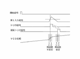
図15は第5の実施形態による半導体装置1の概略構成を示すブロック図、図16は第5の実施形態による半導体装置1の入出力タイミングを示す信号波形図である。図15の半導体装置1は、図13の半導体装置1の構成に加えて、遅延器26を備えている。遅延器26は、比較器6から出力された第2入力信号を所定時間遅延させる。所定時間とは、第1入力信号に含まれる反射光成分に対応する信号領域が終わるまでの時間である必要がある。より具体的には、所定時間は、反射光成分を含む信号領域が終わって、VCO2の発振信号の発振周波数が安定するまでの時間であるのが望ましい。
FIG. 15 is a block diagram showing a schematic configuration of the
遅延器26で第2入力信号を所定時間遅延させることで、本来は図16の時刻t1で第2信号が遷移する(トリガ信号が出る)のに対して、時刻t1から所定時間遅延した時刻t2で第2信号が遷移する(トリガ信号が出る)。時刻t2での発振信号がクロック周期内でそれほど周波数が変化せず安定している場合には、第1位相サンプラ11と第2位相サンプラ12は、第1位相デジタル信号DPAと第2位相デジタル信号DPTを精度よく生成することができる。
By delaying the second input signal by the
図17は図15の一変形例による半導体装置1の概略構成を示すブロック図である。図17の半導体装置1は、図13の半導体装置1の構成に加えて、VCO2の前段側に遅延器26を追加したものである。遅延器26は、第1入力信号を所定時間遅延させた後にVCO2に入力する。VCO2は、第1入力信号を所定時間遅延させた遅延入力信号に基づいて周波数変調された発振信号を出力する。
FIG. 17 is a block diagram showing a schematic configuration of a
比較器6は、遅延されていない元の第1入力信号に基づいて第2入力信号を生成する。第1位相サンプラ11と第2位相サンプラ12は、遅延入力信号に基づいて周波数変調された発振信号に基づいて第1位相デジタル信号DPAと第2位相デジタル信号DPTを出力する。第1位相デジタル信号DPAと第2位相デジタル信号DPTは、第2入力信号の遷移タイミングよりも所定時間遅れている。よって、第1位相デジタル信号DPAと第2位相デジタル信号DPTは、安定化した発振信号に基づいて生成されるため、図15と同様に、発振信号が安定化した後に第1位相デジタル信号DPAと第2位相デジタル信号DPTを生成できる。
このように、第5の実施形態では、遅延器26を設けて、比較器6で生成した第2入力信号を所定時間遅延させるか、あるいはVCO2に入力される第1入力信号を所定時間遅延させるため、VCO2の発振信号の発振周波数が安定化した後に、第1位相サンプラ11と第2位相サンプラ12により、第1位相デジタル信号DPAと第2位相デジタル信号DPTを生成できる。
Thus, in the fifth embodiment, the
(第6の実施形態)
図18は第6の実施形態による半導体装置1の概略構成を示すブロック図である。図18の半導体装置1は、図7の半導体装置1の構成に加えて、DA変換器(DAC:Digital Analog Converter)27と、差分器28と、ループフィルタ29とを備えている。DAC27は、第1位相サンプラ11から出力された第1位相デジタル信号DPAを位相アナログ信号に変換する。差分器28は、第1入力信号とDAC27の出力信号と第1入力信号との差信号を出力する。ループフィルタ29は、この差信号を積分した信号を、第1入力信号の代わりにVCO2に入力する。ループフィルタ29は積分器として機能する。
(Sixth embodiment)
FIG. 18 is a block diagram showing a schematic configuration of a
図18の半導体装置1では、VCO2と第1位相サンプラ11とで、デルタ-シグマAD変換器を構成している。第1位相デジタル信号DPAをDAC27とループフィルタ29にて、VCO2の入力側に帰還させるため、AD変換時の量子化雑音をより低減できる。
In the
なお、図18のDAC27と差分器28は、図15や図17の半導体装置1に付加してもよい。
18 may be added to the
本発明のいくつかの実施形態を説明したが、これらの実施形態は、例として提示したものであり、発明の範囲を限定することは意図していない。これら新規な実施形態は、その他の様々な形態で実施されることが可能であり、発明の要旨を逸脱しない範囲で、種々の省略、置き換え、変更を行うことができる。これら実施形態やその変形は、発明の範囲や要旨に含まれるとともに、特許請求の範囲に記載された発明とその均等の範囲に含まれる。 While several embodiments of the invention have been described, these embodiments have been presented by way of example and are not intended to limit the scope of the invention. These novel embodiments can be implemented in various other forms, and various omissions, replacements, and modifications can be made without departing from the scope of the invention. These embodiments and modifications thereof are included in the scope and gist of the invention, and are included in the scope of the invention described in the claims and equivalents thereof.
1 半導体装置、2 発振器、3 周期数計測器、3a カウンタ、4 第1演算器、4a FF、5 第2演算器、5a FF、6 比較器、7 算出器、10 演算器、11 第1位相サンプラ、12 第2位相サンプラ、13 第3位相サンプラ、14 リング発振器、15 PMOSトランジスタ、19 物体、20 距離計測装置、21 制御部、22 光源、23 光検出器、24 AFE部、25 算出器、26 遅延器
REFERENCE SIGNS
Claims (12)
前記発振信号の周期数を計測する周期数計測器と、
クロック信号の第1クロック周期に、前記周期数計測器で計測された第1周期数に基づいて、前記第1入力信号をデジタル変換した第1デジタル信号を出力する第1演算器と、
前記クロック信号の基準時点から第2入力信号が遷移するタイミングまでの期間に、前記周期数計測器で計測された第2周期数に基づいて、第2デジタル信号を出力する第2演算器と、を備える、半導体装置。 an oscillator that outputs an oscillation signal whose frequency is modulated according to the first input signal;
a periodicity measuring instrument for measuring the periodicity of the oscillation signal;
a first arithmetic unit that outputs a first digital signal obtained by digitally converting the first input signal based on the first period number measured by the period number measuring device in the first clock period of the clock signal;
a second computing unit that outputs a second digital signal based on the second period number measured by the period number measuring device during the period from the reference time point of the clock signal to the transition timing of the second input signal; A semiconductor device comprising:
クロック信号のクロック周期に前記発振信号の位相をサンプリングした第1位相デジタル信号を出力する第1位相サンプラと、
第2入力信号が遷移したタイミングで前記発振信号の位相をサンプリングした第2位相デジタル信号を出力する第2位相サンプラと、
前記第2入力信号が遷移したタイミングで前記クロック信号の位相をサンプリングした第3位相デジタル信号を出力する第3位相サンプラと、
前記第1位相デジタル信号に基づいて、前記第1入力信号をデジタル変換した第1デジタル信号を生成する第1演算器と、
前記第1、第2及び第3位相デジタル信号に基づいて、前記第2入力信号が遷移するタイミングまでの期間に応じた第2デジタル信号を生成する第2演算器と、を備える、半導体装置。 an oscillator that outputs an oscillation signal whose frequency is modulated according to the first input signal;
a first phase sampler that outputs a first phase digital signal obtained by sampling the phase of the oscillation signal at the clock cycle of the clock signal;
a second phase sampler that outputs a second phase digital signal obtained by sampling the phase of the oscillation signal at the timing of transition of the second input signal;
a third phase sampler that outputs a third phase digital signal obtained by sampling the phase of the clock signal at the timing of transition of the second input signal;
a first calculator that generates a first digital signal obtained by digitally converting the first input signal based on the first phase digital signal;
and a second calculator that generates a second digital signal corresponding to a period up to a transition timing of the second input signal based on the first, second, and third phase digital signals.
前記第2演算器は、前記第2位相デジタル信号に近接した2以上の前記第1位相デジタル信号を内挿する処理と前記第3位相デジタル信号とに基づいて、前記第2デジタル信号を生成する、請求項4に記載の半導体装置。 The first calculator generates the first digital signal by time differentiating the first phase digital signal,
The second computing unit generates the second digital signal based on a process of interpolating two or more of the first phase digital signals close to the second phase digital signal and the third phase digital signal. 5. The semiconductor device according to claim 4.
前記第2位相サンプラは、前記遅延器で遅延された第2入力信号が遷移したタイミングで前記第2位相デジタル信号を出力し、
前記第3位相サンプラは、前記遅延された第2入力信号が遷移したタイミングで前記第3位相デジタル信号を出力する、請求項4乃至6のいずれか一項に記載の半導体装置。 A delay device for delaying the second input signal,
The second phase sampler outputs the second phase digital signal at the timing when the second input signal delayed by the delay device transitions,
7. The semiconductor device according to claim 4, wherein said third phase sampler outputs said third phase digital signal at timing when said delayed second input signal transitions.
前記発振器は、前記遅延器で遅延された第1入力信号の信号レベルに応じて周波数が変調された前記発振信号を出力する、請求項4乃至6のいずれか一項に記載の半導体装置。 A delay device for delaying the first input signal;
7. The semiconductor device according to claim 4, wherein said oscillator outputs said oscillation signal whose frequency is modulated according to the signal level of said first input signal delayed by said delay device.
前記第1入力信号と前記位相アナログ信号との差信号を積分した信号を前記第1入力信号の代わりに前記発振器に入力するループフィルタと、を備える請求項4乃至10のいずれか一項に記載の半導体装置。 a DA converter that converts the first phase digital signal into a phase analog signal;
11. The loop filter according to any one of claims 4 to 10, further comprising a loop filter that inputs a signal obtained by integrating a difference signal between said first input signal and said phase analog signal to said oscillator instead of said first input signal. semiconductor equipment.
前記第1光信号が物体で反射された反射光信号を含む第2光信号を受光して、電気信号である前記第1入力信号に変換する光検出器と、
請求項1乃至11のいずれか一項に記載の半導体装置を有し、前記第1入力信号に基づいて、前記反射光信号の受光タイミングを表す前記第1デジタル信号及び前記第2デジタル信号を出力するフロントエンド部と、
前記第1デジタル信号及び前記第2デジタル信号に基づいて、前記開始信号のタイミングから前記第2入力信号が入力されるまでの時間を計測し、計測された時間に基づいて、前記物体までの距離を計測する距離演算部と、を備える、距離計測装置。 a light source that emits the first optical signal in synchronization with the timing of the start signal;
a photodetector that receives a second optical signal including a reflected optical signal in which the first optical signal is reflected by an object and converts the second optical signal into the first input signal that is an electrical signal;
12. The semiconductor device according to claim 1, wherein the first digital signal and the second digital signal representing light reception timing of the reflected light signal are output based on the first input signal. a front end that
Based on the first digital signal and the second digital signal, the time from the timing of the start signal to the input of the second input signal is measured, and the distance to the object is calculated based on the measured time. A distance measuring device, comprising: a distance calculating unit that measures
Priority Applications (5)
| Application Number | Priority Date | Filing Date | Title |
|---|---|---|---|
| JP2018216715A JP7169171B2 (en) | 2018-11-19 | 2018-11-19 | Semiconductor device and distance measuring device |
| DE102019212999.4A DE102019212999B4 (en) | 2018-11-19 | 2019-08-29 | SEMICONDUCTOR CIRCUIT AND DISTANCE MEASURING DEVICE |
| US16/562,817 US11573321B2 (en) | 2018-11-19 | 2019-09-06 | Semiconductor circuitry and distance measuring device |
| CN201910861327.0A CN111273308B (en) | 2018-11-19 | 2019-09-12 | Semiconductor circuits and distance measuring devices |
| JP2022170980A JP7431924B2 (en) | 2018-11-19 | 2022-10-25 | Semiconductor circuit and distance measuring device |
Applications Claiming Priority (1)
| Application Number | Priority Date | Filing Date | Title |
|---|---|---|---|
| JP2018216715A JP7169171B2 (en) | 2018-11-19 | 2018-11-19 | Semiconductor device and distance measuring device |
Related Child Applications (1)
| Application Number | Title | Priority Date | Filing Date |
|---|---|---|---|
| JP2022170980A Division JP7431924B2 (en) | 2018-11-19 | 2022-10-25 | Semiconductor circuit and distance measuring device |
Publications (2)
| Publication Number | Publication Date |
|---|---|
| JP2020085537A JP2020085537A (en) | 2020-06-04 |
| JP7169171B2 true JP7169171B2 (en) | 2022-11-10 |
Family
ID=70470363
Family Applications (2)
| Application Number | Title | Priority Date | Filing Date |
|---|---|---|---|
| JP2018216715A Active JP7169171B2 (en) | 2018-11-19 | 2018-11-19 | Semiconductor device and distance measuring device |
| JP2022170980A Active JP7431924B2 (en) | 2018-11-19 | 2022-10-25 | Semiconductor circuit and distance measuring device |
Family Applications After (1)
| Application Number | Title | Priority Date | Filing Date |
|---|---|---|---|
| JP2022170980A Active JP7431924B2 (en) | 2018-11-19 | 2022-10-25 | Semiconductor circuit and distance measuring device |
Country Status (4)
| Country | Link |
|---|---|
| US (1) | US11573321B2 (en) |
| JP (2) | JP7169171B2 (en) |
| CN (1) | CN111273308B (en) |
| DE (1) | DE102019212999B4 (en) |
Families Citing this family (2)
| Publication number | Priority date | Publication date | Assignee | Title |
|---|---|---|---|---|
| JP7169171B2 (en) * | 2018-11-19 | 2022-11-10 | 株式会社東芝 | Semiconductor device and distance measuring device |
| JP7527946B2 (en) * | 2020-12-11 | 2024-08-05 | 株式会社東芝 | Oscillator circuit, time-to-digital converter, and electronic device |
Citations (3)
| Publication number | Priority date | Publication date | Assignee | Title |
|---|---|---|---|---|
| JP2000028721A (en) | 1998-07-14 | 2000-01-28 | Minolta Co Ltd | Range finder |
| JP2003139857A (en) | 2001-11-01 | 2003-05-14 | Nec Eng Ltd | Laser distance measuring apparatus |
| JP2017063433A (en) | 2010-01-15 | 2017-03-30 | 株式会社半導体エネルギー研究所 | Semiconductor device |
Family Cites Families (17)
| Publication number | Priority date | Publication date | Assignee | Title |
|---|---|---|---|---|
| JPH01170221A (en) | 1987-12-25 | 1989-07-05 | Mitsubishi Electric Corp | Analog digital converter |
| JPH01208024A (en) * | 1988-02-16 | 1989-08-22 | Nippon Telegr & Teleph Corp <Ntt> | Quantizer |
| JPH0415593A (en) * | 1990-05-09 | 1992-01-20 | Nikon Corp | High resolution time difference measuring instrument |
| JP2757600B2 (en) | 1991-07-30 | 1998-05-25 | 株式会社デンソー | Time A / D conversion circuit |
| JP2002100967A (en) * | 2000-03-17 | 2002-04-05 | Sony Corp | Power supply voltage control device, semiconductor device and driving method thereof |
| JP2005182872A (en) * | 2003-12-17 | 2005-07-07 | Toshiba Corp | Nonvolatile semiconductor memory device |
| US8045670B2 (en) * | 2007-06-22 | 2011-10-25 | Texas Instruments Incorporated | Interpolative all-digital phase locked loop |
| JP4729054B2 (en) * | 2008-01-28 | 2011-07-20 | 株式会社東芝 | Semiconductor integrated circuit for communication |
| JP2012060603A (en) * | 2010-09-13 | 2012-03-22 | Toshiba Corp | Semiconductor integrated circuit and radio communication equipment |
| EP2597483B8 (en) * | 2011-11-25 | 2017-06-07 | Safran Vectronix AG | Distance sensor |
| US9632179B2 (en) * | 2012-07-04 | 2017-04-25 | Blackberry Limited | Estimating a baseline of a proximity sensor |
| EP3260881B1 (en) * | 2015-02-19 | 2021-04-21 | Mitsubishi Electric Corporation | Fm-cw radar and fm-cw signal generation method |
| CN105044678B (en) * | 2015-06-26 | 2017-11-17 | 复旦大学 | Radar response based on all-digital phase-locked loop framework/interference one wireless communication device |
| US10191154B2 (en) * | 2016-02-11 | 2019-01-29 | Massachusetts Institute Of Technology | Methods and apparatus for time-of-flight imaging |
| CN106950539B (en) * | 2017-03-03 | 2020-05-12 | 长沙理工大学 | High-precision anti-GPS tracking module positioning and identification method based on time difference method |
| US10007001B1 (en) * | 2017-03-28 | 2018-06-26 | Luminar Technologies, Inc. | Active short-wave infrared four-dimensional camera |
| JP7169171B2 (en) | 2018-11-19 | 2022-11-10 | 株式会社東芝 | Semiconductor device and distance measuring device |
-
2018
- 2018-11-19 JP JP2018216715A patent/JP7169171B2/en active Active
-
2019
- 2019-08-29 DE DE102019212999.4A patent/DE102019212999B4/en active Active
- 2019-09-06 US US16/562,817 patent/US11573321B2/en active Active
- 2019-09-12 CN CN201910861327.0A patent/CN111273308B/en active Active
-
2022
- 2022-10-25 JP JP2022170980A patent/JP7431924B2/en active Active
Patent Citations (3)
| Publication number | Priority date | Publication date | Assignee | Title |
|---|---|---|---|---|
| JP2000028721A (en) | 1998-07-14 | 2000-01-28 | Minolta Co Ltd | Range finder |
| JP2003139857A (en) | 2001-11-01 | 2003-05-14 | Nec Eng Ltd | Laser distance measuring apparatus |
| JP2017063433A (en) | 2010-01-15 | 2017-03-30 | 株式会社半導体エネルギー研究所 | Semiconductor device |
Also Published As
| Publication number | Publication date |
|---|---|
| JP7431924B2 (en) | 2024-02-15 |
| DE102019212999B4 (en) | 2025-05-08 |
| CN111273308B (en) | 2023-10-20 |
| CN111273308A (en) | 2020-06-12 |
| DE102019212999A1 (en) | 2020-05-20 |
| JP2022186902A (en) | 2022-12-15 |
| US20200158872A1 (en) | 2020-05-21 |
| JP2020085537A (en) | 2020-06-04 |
| US11573321B2 (en) | 2023-02-07 |
Similar Documents
| Publication | Publication Date | Title |
|---|---|---|
| JP3935897B2 (en) | Lightwave ranging device | |
| KR102631502B1 (en) | analog-to-digital converter | |
| JP7431924B2 (en) | Semiconductor circuit and distance measuring device | |
| KR100982103B1 (en) | Time-to-digital converters, time-to-digital conversion methods, and computer readable storage media | |
| US11079723B2 (en) | Apparatus and methods for automatic time measurements | |
| US8879048B2 (en) | Device and method for determining the distance to an object | |
| Keränen et al. | A wide range, 4.2 ps (rms) precision CMOS TDC with cyclic interpolators based on switched-frequency ring oscillators | |
| US10534322B2 (en) | Use of ring oscillators for multi-stop time measurements | |
| US20240142584A1 (en) | Lidar time-of-flight signal processing | |
| CN110622038A (en) | Optical sensor, electronic device, arithmetic device, and method for measuring distance between optical sensor and detection object | |
| US10725433B2 (en) | Time-to-digital conversion circuitry | |
| JPWO2017208651A1 (en) | Optical sensor and electronic device | |
| CN109945950B (en) | Precision ADC Sampling Clock for High Precision Wireless Guided Wave Radar | |
| US10972116B2 (en) | Time to digital converter and A/D conversion circuit | |
| CN111033307B (en) | Sensor device and measurement method | |
| Arvani et al. | Peak-SNR analysis of CMOS TDCs for SPAD-based TCSPC 3D imaging applications | |
| US10677648B2 (en) | Optical sensor and electronic device | |
| WO2019176751A1 (en) | Light detection device, light detection method and optical distance sensor | |
| JP2004226069A (en) | Ranging device | |
| JP5416978B2 (en) | Flying object | |
| Lee et al. | A laser ranging radar transceiver with modulated evaluation clock in 65nm CMOS technology | |
| JP2004325373A (en) | Distance measuring instrument | |
| JP2025079842A (en) | Time measurement circuit, distance measuring device, and time measurement method | |
| JP5509624B2 (en) | Signal generator | |
| JP2024102734A (en) | Distance measuring device |
Legal Events
| Date | Code | Title | Description |
|---|---|---|---|
| A621 | Written request for application examination |
Free format text: JAPANESE INTERMEDIATE CODE: A621 Effective date: 20210804 |
|
| A977 | Report on retrieval |
Free format text: JAPANESE INTERMEDIATE CODE: A971007 Effective date: 20220830 |
|
| TRDD | Decision of grant or rejection written | ||
| A01 | Written decision to grant a patent or to grant a registration (utility model) |
Free format text: JAPANESE INTERMEDIATE CODE: A01 Effective date: 20220930 |
|
| A61 | First payment of annual fees (during grant procedure) |
Free format text: JAPANESE INTERMEDIATE CODE: A61 Effective date: 20221028 |
|
| R150 | Certificate of patent or registration of utility model |
Ref document number: 7169171 Country of ref document: JP Free format text: JAPANESE INTERMEDIATE CODE: R150 |