JP7153574B2 - Top electrode structure, plasma processing apparatus, and method of assembling top electrode structure - Google Patents
Top electrode structure, plasma processing apparatus, and method of assembling top electrode structure Download PDFInfo
- Publication number
- JP7153574B2 JP7153574B2 JP2019006074A JP2019006074A JP7153574B2 JP 7153574 B2 JP7153574 B2 JP 7153574B2 JP 2019006074 A JP2019006074 A JP 2019006074A JP 2019006074 A JP2019006074 A JP 2019006074A JP 7153574 B2 JP7153574 B2 JP 7153574B2
- Authority
- JP
- Japan
- Prior art keywords
- electrode
- plate
- gas
- hole
- plasma processing
- Prior art date
- Legal status (The legal status is an assumption and is not a legal conclusion. Google has not performed a legal analysis and makes no representation as to the accuracy of the status listed.)
- Active
Links
Images


Classifications
-
- H—ELECTRICITY
- H01—ELECTRIC ELEMENTS
- H01J—ELECTRIC DISCHARGE TUBES OR DISCHARGE LAMPS
- H01J37/00—Discharge tubes with provision for introducing objects or material to be exposed to the discharge, e.g. for the purpose of examination or processing thereof
- H01J37/32—Gas-filled discharge tubes
- H01J37/32431—Constructional details of the reactor
- H01J37/32532—Electrodes
- H01J37/32559—Protection means, e.g. coatings
-
- H—ELECTRICITY
- H01—ELECTRIC ELEMENTS
- H01J—ELECTRIC DISCHARGE TUBES OR DISCHARGE LAMPS
- H01J37/00—Discharge tubes with provision for introducing objects or material to be exposed to the discharge, e.g. for the purpose of examination or processing thereof
- H01J37/32—Gas-filled discharge tubes
- H01J37/32009—Arrangements for generation of plasma specially adapted for examination or treatment of objects, e.g. plasma sources
- H01J37/32082—Radio frequency generated discharge
- H01J37/32091—Radio frequency generated discharge the radio frequency energy being capacitively coupled to the plasma
-
- H—ELECTRICITY
- H01—ELECTRIC ELEMENTS
- H01J—ELECTRIC DISCHARGE TUBES OR DISCHARGE LAMPS
- H01J37/00—Discharge tubes with provision for introducing objects or material to be exposed to the discharge, e.g. for the purpose of examination or processing thereof
- H01J37/32—Gas-filled discharge tubes
- H01J37/32431—Constructional details of the reactor
- H01J37/3244—Gas supply means
- H01J37/32449—Gas control, e.g. control of the gas flow
-
- H—ELECTRICITY
- H01—ELECTRIC ELEMENTS
- H01J—ELECTRIC DISCHARGE TUBES OR DISCHARGE LAMPS
- H01J37/00—Discharge tubes with provision for introducing objects or material to be exposed to the discharge, e.g. for the purpose of examination or processing thereof
- H01J37/32—Gas-filled discharge tubes
- H01J37/32431—Constructional details of the reactor
- H01J37/32458—Vessel
- H01J37/32513—Sealing means, e.g. sealing between different parts of the vessel
-
- H—ELECTRICITY
- H01—ELECTRIC ELEMENTS
- H01J—ELECTRIC DISCHARGE TUBES OR DISCHARGE LAMPS
- H01J37/00—Discharge tubes with provision for introducing objects or material to be exposed to the discharge, e.g. for the purpose of examination or processing thereof
- H01J37/32—Gas-filled discharge tubes
- H01J37/32431—Constructional details of the reactor
- H01J37/32458—Vessel
- H01J37/32522—Temperature
-
- H—ELECTRICITY
- H01—ELECTRIC ELEMENTS
- H01J—ELECTRIC DISCHARGE TUBES OR DISCHARGE LAMPS
- H01J37/00—Discharge tubes with provision for introducing objects or material to be exposed to the discharge, e.g. for the purpose of examination or processing thereof
- H01J37/32—Gas-filled discharge tubes
- H01J37/32431—Constructional details of the reactor
- H01J37/32532—Electrodes
- H01J37/32541—Shape
-
- H—ELECTRICITY
- H01—ELECTRIC ELEMENTS
- H01J—ELECTRIC DISCHARGE TUBES OR DISCHARGE LAMPS
- H01J37/00—Discharge tubes with provision for introducing objects or material to be exposed to the discharge, e.g. for the purpose of examination or processing thereof
- H01J37/32—Gas-filled discharge tubes
- H01J37/32431—Constructional details of the reactor
- H01J37/32532—Electrodes
- H01J37/32568—Relative arrangement or disposition of electrodes; moving means
-
- H—ELECTRICITY
- H01—ELECTRIC ELEMENTS
- H01J—ELECTRIC DISCHARGE TUBES OR DISCHARGE LAMPS
- H01J37/00—Discharge tubes with provision for introducing objects or material to be exposed to the discharge, e.g. for the purpose of examination or processing thereof
- H01J37/32—Gas-filled discharge tubes
- H01J37/32431—Constructional details of the reactor
- H01J37/32623—Mechanical discharge control means
- H01J37/32651—Shields, e.g. dark space shields, Faraday shields
-
- H—ELECTRICITY
- H01—ELECTRIC ELEMENTS
- H01J—ELECTRIC DISCHARGE TUBES OR DISCHARGE LAMPS
- H01J37/00—Discharge tubes with provision for introducing objects or material to be exposed to the discharge, e.g. for the purpose of examination or processing thereof
- H01J37/32—Gas-filled discharge tubes
- H01J37/32431—Constructional details of the reactor
- H01J37/32715—Workpiece holder
-
- H—ELECTRICITY
- H01—ELECTRIC ELEMENTS
- H01J—ELECTRIC DISCHARGE TUBES OR DISCHARGE LAMPS
- H01J37/00—Discharge tubes with provision for introducing objects or material to be exposed to the discharge, e.g. for the purpose of examination or processing thereof
- H01J37/32—Gas-filled discharge tubes
- H01J37/32431—Constructional details of the reactor
- H01J37/32798—Further details of plasma apparatus not provided for in groups H01J37/3244 - H01J37/32788; special provisions for cleaning or maintenance of the apparatus
- H01J37/32816—Pressure
- H01J37/32834—Exhausting
-
- H—ELECTRICITY
- H01—ELECTRIC ELEMENTS
- H01L—SEMICONDUCTOR DEVICES NOT COVERED BY CLASS H10
- H01L21/00—Processes or apparatus adapted for the manufacture or treatment of semiconductor or solid state devices or of parts thereof
- H01L21/67—Apparatus specially adapted for handling semiconductor or electric solid state devices during manufacture or treatment thereof; Apparatus specially adapted for handling wafers during manufacture or treatment of semiconductor or electric solid state devices or components ; Apparatus not specifically provided for elsewhere
- H01L21/683—Apparatus specially adapted for handling semiconductor or electric solid state devices during manufacture or treatment thereof; Apparatus specially adapted for handling wafers during manufacture or treatment of semiconductor or electric solid state devices or components ; Apparatus not specifically provided for elsewhere for supporting or gripping
- H01L21/6831—Apparatus specially adapted for handling semiconductor or electric solid state devices during manufacture or treatment thereof; Apparatus specially adapted for handling wafers during manufacture or treatment of semiconductor or electric solid state devices or components ; Apparatus not specifically provided for elsewhere for supporting or gripping using electrostatic chucks
- H01L21/6833—Details of electrostatic chucks
Description
本開示の例示的実施形態は、上部電極構造、プラズマ処理装置、及び上部電極構造を組み立てる方法に関する。 SUMMARY Exemplary embodiments of the present disclosure relate to top electrode structures, plasma processing apparatus, and methods of assembling top electrode structures.
特許文献1は、プラズマ処理装置の上部電極において電極プレートを吸着する構造を開示する。電極プレートと、電極プレートに接触するプレートとの間には、静電吸着部が介在する。静電吸着部は、セラミック製であり、プレートの下面にクランプを介して固定される。 Patent Literature 1 discloses a structure for attracting an electrode plate in an upper electrode of a plasma processing apparatus. An electrostatic attraction part is interposed between the electrode plate and the plate in contact with the electrode plate. The electrostatic attraction part is made of ceramic and fixed to the lower surface of the plate via a clamp.
本開示は、ラジカル又はガスによる静電吸着部の消耗を改善する技術を提供する。 The present disclosure provides a technique for improving the consumption of electrostatic adsorption parts by radicals or gases.
一つの例示的実施形態において、プラズマ処理装置の上部電極構造が提供される。上部電極構造は、電極プレート、ガスプレート、静電吸着部、及び遮蔽構造を備える。電極プレートは、厚さ方向に貫通するガス吐出孔が形成される。ガスプレートは、ガス吐出孔に処理ガスを供給するガス流路がガス吐出孔と対向する位置に厚さ方向に延びるように形成される。静電吸着部は、電極プレートとガスプレートとの間に介在し、ガスプレートの下面と接触する接触面と電極プレートの上面を吸着する吸着面とを有する。遮蔽構造は、ガス吐出孔から電極プレートとガスプレートとの間へ移動するラジカル又はガスを遮蔽する。 In one exemplary embodiment, an upper electrode structure for a plasma processing apparatus is provided. The upper electrode structure comprises an electrode plate, a gas plate, an electrostatic adsorption part and a shielding structure. The electrode plate is formed with gas discharge holes penetrating in the thickness direction. The gas plate is formed such that gas flow paths for supplying process gas to the gas ejection holes extend in the thickness direction at positions facing the gas ejection holes. The electrostatic attraction part is interposed between the electrode plate and the gas plate, and has a contact surface that contacts the lower surface of the gas plate and an attraction surface that attracts the upper surface of the electrode plate. The shielding structure shields radicals or gas moving from the gas ejection holes to between the electrode plate and the gas plate.
一つの例示的実施形態によれば、ラジカル又はガスによる静電吸着部の消耗を改善することができる。 According to one exemplary embodiment, the consumption of the electrostatic adsorption portion by radicals or gases can be improved.
以下、種々の例示的実施形態について説明する。 Various exemplary embodiments are described below.
一つの例示的実施形態において、プラズマ処理装置の上部電極構造が提供される。上部電極構造は、電極プレート、ガスプレート、静電吸着部、及び遮蔽構造を備える。電極プレートには、厚さ方向に貫通するガス吐出孔が形成される。ガスプレートには、ガス吐出孔に処理ガスを供給するガス流路がガス吐出孔と対向する位置に厚さ方向に延びるように形成される。静電吸着部は、電極プレートとガスプレートとの間に介在し、ガスプレートの下面と接触する接触面と電極プレートの上面を吸着する吸着面とを有する。遮蔽構造は、ガス吐出孔から電極プレートとガスプレートとの間へ移動するラジカル又はガスを遮蔽する。 In one exemplary embodiment, an upper electrode structure for a plasma processing apparatus is provided. The upper electrode structure comprises an electrode plate, a gas plate, an electrostatic adsorption part and a shielding structure. A gas ejection hole is formed through the electrode plate in the thickness direction. In the gas plate, a gas passage for supplying a processing gas to the gas ejection holes is formed so as to extend in the thickness direction at a position facing the gas ejection holes. The electrostatic attraction part is interposed between the electrode plate and the gas plate, and has a contact surface that contacts the lower surface of the gas plate and an attraction surface that attracts the upper surface of the electrode plate. The shielding structure shields radicals or gas moving from the gas ejection holes to between the electrode plate and the gas plate.
電極プレートとガスプレートとの間に静電吸着部を介在させた場合、電極プレートのガス吐出孔の上端とガスプレートのガス流路の下端との間に隙間が生じる。電極プレートはプラズマに面しているため、ラジカル又はガスが、電極プレートのガス吐出孔から侵入し、上述した隙間に入り込むおそれがある。このようなラジカル又はガスは、静電吸着部を侵食し摩耗させるおそれがある。 When the electrostatic adsorption portion is interposed between the electrode plate and the gas plate, a gap is generated between the upper end of the gas discharge hole of the electrode plate and the lower end of the gas flow channel of the gas plate. Since the electrode plate faces the plasma, there is a risk that radicals or gases may enter through the gas ejection holes of the electrode plate and enter the gaps described above. Such radicals or gases may erode and wear the electrostatic adsorption portion.
この上部電極構造においては、遮蔽構造により、ガス吐出孔から電極プレートとガスプレートとの間へ移動するラジカル又はガスが遮蔽される。よって、この上部電極構造は、ラジカル又はガスによる静電吸着部の消耗を改善することができる。 In this upper electrode structure, the shielding structure shields radicals or gas moving from the gas ejection holes to between the electrode plate and the gas plate. Therefore, this upper electrode structure can improve the consumption of the electrostatic adsorption portion by radicals or gas.
一つの例示的実施形態において、遮蔽構造は、電極プレートとガスプレートとの間に介在し、ガス吐出孔の上端とガス流路の下端とを接続する接続部材を有してもよい。この例示的実施形態によれば、接続部材により、ガス吐出孔から電極プレートとガスプレートとの間へ移動するラジカル又はガスを物理的に遮蔽することができる。 In one exemplary embodiment, the shielding structure may have a connection member interposed between the electrode plate and the gas plate and connecting the upper end of the gas discharge hole and the lower end of the gas channel. According to this exemplary embodiment, the connecting member can physically shield radicals or gases moving between the electrode plate and the gas plate from the gas ejection holes.
一つの例示的実施形態において、ガスプレートは、その下面に、静電吸着部の接触面と対向する第1領域と、ガス吐出孔と対向する第2領域とを有してもよい。接続部材は、その上端がガスプレートの下面の第2領域に接続され、その下端が電極プレートの上面に接続されてもよい。接続部材は、その内部にガス吐出孔とガス流路とを連通する流路を画成してもよい。この例示的実施形態によれば、接続部材により、ガス吐出孔から電極プレートとガスプレートとの間へ移動するラジカル又はガスを物理的に遮蔽しつつ、ガス吐出孔とガス流路とを連通させることができる。 In one exemplary embodiment, the gas plate may have a first region facing the contact surface of the electrostatic attraction part and a second region facing the gas ejection holes on its lower surface. The connection member may have its upper end connected to the second region of the lower surface of the gas plate and its lower end connected to the upper surface of the electrode plate. The connection member may define therein a flow path that communicates the gas discharge hole and the gas flow path. According to this exemplary embodiment, the connection member physically shields radicals or gas moving between the electrode plate and the gas plate from the gas ejection holes, while allowing the gas ejection holes and the gas flow paths to communicate with each other. be able to.
一つの例示的実施形態において、接続部材は、ガスプレート及び電極プレートの何れか一方と一体的に形成されてもよい。この例示的実施形態によれば、部品数を増加させることなく、ラジカル又はガスによる静電吸着部の消耗を改善することができる。 In one exemplary embodiment, the connection member may be integrally formed with either one of the gas plate and the electrode plate. According to this exemplary embodiment, it is possible to improve the consumption of the electrostatic adsorption part by radicals or gas without increasing the number of parts.
一つの例示的実施形態において、接続部材は、ガスプレートと一体的に形成された上部材と、上部材と接触し電極プレートと一体的に形成された下部材とを有してもよい。この例示的実施形態によれば、部品数を増加させることなく、ラジカル又はガスによる静電吸着部の消耗を改善することができる。 In one exemplary embodiment, the connection member may have an upper member integrally formed with the gas plate and a lower member in contact with the upper member and integrally formed with the electrode plate. According to this exemplary embodiment, it is possible to improve the consumption of the electrostatic adsorption part by radicals or gas without increasing the number of parts.
一つの例示的実施形態において、ガスプレートは、電極プレートとの接触箇所に不働態層を有してもよい。この例示的実施形態によれば、ガスプレートと電極プレートとの接触箇所の変質を防止することができる。 In one exemplary embodiment, the gas plate may have a passivation layer at the point of contact with the electrode plate. According to this exemplary embodiment, deterioration of the contact points between the gas plate and the electrode plate can be prevented.
一つの例示的実施形態において、接続部材は、電極プレート及びガスプレートとは別体で形成されてもよい。この例示的実施形態によれば、既存の電極プレート及びガスプレートに変更を加えることなく、ラジカル又はガスによる静電吸着部の消耗を改善することができる。 In one exemplary embodiment, the connecting member may be formed separately from the electrode plate and the gas plate. According to this exemplary embodiment, it is possible to improve the consumption of the electrostatic adsorption portion by radicals or gases without modifying the existing electrode plate and gas plate.
一つの例示的実施形態において、静電吸着部は、弾性を有する誘電体からなる本体部と、本体部の内部に配置された電極とを有してもよい。静電吸着部は、電極プレートとガスプレートとの間に本体部が圧縮された状態で配置され、圧縮された本体部は接続部材と同一の厚さを有する。この例示的実施形態によれば、電極プレートとガスプレートとの接触に干渉することなく、静電吸着部を配置することができる。 In one exemplary embodiment, the electrostatic attraction part may have a main body made of an elastic dielectric material and an electrode arranged inside the main body. The electrostatic adsorption part is arranged between the electrode plate and the gas plate with the main body part compressed, and the compressed main body part has the same thickness as the connection member. According to this exemplary embodiment, the electrostatic chuck can be placed without interfering with the contact between the electrode plate and the gas plate.
一つの例示的実施形態において、ガスプレートは、その下面に、静電吸着部の接触面と対向する第1領域と、ガス吐出孔と対向する第2領域とを有してもよい。第2領域と電極プレートの上面とによって隙間が形成されてもよい。遮蔽構造は、減圧可能な排気装置と、排気装置に接続される排気流路とを有し得る。排気流路は、ガスプレートに形成され、その下端が第2領域に位置してもよい。排気装置は、排気流路を介して隙間の空間を減圧してもよい。この例示的実施形態によれば、ガス吐出孔から電極プレートとガスプレートとの間へ移動するラジカル又はガスを、静電吸着部に到達する前に排気流路から吸引することができる。よって、ラジカル又はガスによる静電吸着部の消耗を改善することができる。 In one exemplary embodiment, the gas plate may have a first region facing the contact surface of the electrostatic attraction part and a second region facing the gas ejection holes on its lower surface. A gap may be formed by the second region and the top surface of the electrode plate. The shielding structure can have a depressurizable exhaust device and an exhaust channel connected to the exhaust device. The exhaust channel may be formed in the gas plate and its lower end may be located in the second region. The exhaust device may depressurize the interstitial space via the exhaust channel. According to this exemplary embodiment, radicals or gases that move between the electrode plate and the gas plate from the gas ejection holes can be sucked from the exhaust channel before reaching the electrostatic adsorption section. Therefore, it is possible to improve the consumption of the electrostatic adsorption portion by radicals or gas.
一つの例示的実施形態において、ガスプレートは、その下面に、静電吸着部の接触面と対向する第1領域と、ガス吐出孔と対向する第2領域とを有してもよい。第2領域と電極プレートの上面とによって隙間が形成されてもよい。遮蔽構造は、遮蔽ガスのガス供給源と、ガス供給源に接続される供給流路とを有してもよい。供給流路は、ガスプレートに形成され、その下端が第2領域に位置し、ガス供給源から遮蔽ガスを隙間の空間へ供給してもよい。この例示的実施形態によれば、ガス吐出孔から電極プレートとガスプレートとの間へ移動するラジカル又はガスを、遮蔽ガスによって静電吸着部に到達する前に遮蔽することができる。よって、ラジカル又はガスによる静電吸着部の消耗を改善することができる。 In one exemplary embodiment, the gas plate may have a first region facing the contact surface of the electrostatic attraction part and a second region facing the gas ejection holes on its lower surface. A gap may be formed by the second region and the top surface of the electrode plate. The shielding structure may have a gas supply of shielding gas and a supply channel connected to the gas supply. A supply channel may be formed in the gas plate, the lower end of which may be located in the second region, to supply the shielding gas from the gas supply source to the interstitial space. According to this exemplary embodiment, radicals or gases moving between the electrode plate and the gas plate from the gas ejection holes can be shielded by the shielding gas before reaching the electrostatic adsorption portion. Therefore, it is possible to improve the consumption of the electrostatic adsorption portion by radicals or gas.
一つの例示的実施形態において、遮蔽ガスの成分は、処理ガスの成分と同一であってもよい。この例示的実施形態によれば、遮蔽ガスがプロセスに与える影響を小さくすることができる。 In one exemplary embodiment, the composition of the shielding gas may be the same as the composition of the process gas. This exemplary embodiment allows the shielding gas to have less impact on the process.
一つの例示的実施形態において、ガスプレートは、冷媒を流通させる流路がその内部に形成されてもよい。この例示的実施形態によれば、ガスプレートを直接的に温度調整することができるので、電極プレートとの熱交換を効率良く行うことができる。 In one exemplary embodiment, the gas plate may have channels formed therein for circulating the coolant. According to this exemplary embodiment, the gas plate can be directly temperature regulated so that heat exchange with the electrode plate can be performed efficiently.
一つの例示的実施形態にかかる上部電極構造は、ガスプレートの上面に接触して配置され、冷媒を流通させる流路が内部に形成された冷却部材をさらに備えてもよい。この例示的実施形態によれば、ガス流路を有するガスプレートを加工することなく、電極プレートを冷却することができる。 The upper electrode structure according to an exemplary embodiment may further include a cooling member disposed in contact with the upper surface of the gas plate and having a flow path for circulating a coolant formed therein. According to this exemplary embodiment, the electrode plate can be cooled without machining the gas plate with the gas channels.
一つの例示的実施形態において、静電吸着部は、第1吸着部と第2吸着部とを有してもよい。第1吸着部は、弾性を有する誘電体からなる第1本体部と、第1本体部の内部に配置された第1電極とを有してもよい。第2吸着部は、弾性を有する誘電体からなる第2本体部と、第2本体部の内部に配置された第2電極とを有してもよい。第1電極及び第2電極には、互いに異なる極性の電圧が印加されてもよい。この例示的実施形態によれば、双極方式で電極プレートを吸着させることができる。 In one exemplary embodiment, the electrostatic attraction part may have a first attraction part and a second attraction part. The first adsorption portion may have a first body made of an elastic dielectric and a first electrode arranged inside the first body. The second adsorption part may have a second body made of an elastic dielectric and a second electrode arranged inside the second body. Voltages with different polarities may be applied to the first electrode and the second electrode. According to this exemplary embodiment, the electrode plates can be attracted in a bipolar fashion.
一つの例示的実施形態において、静電吸着部は、第1吸着部と第2吸着部とを有してもよい。第1吸着部は、弾性を有する誘電体からなる第1本体部と、第1本体部の内部に配置された第1電極とを有してもよい。第2吸着部は、弾性を有する誘電体からなる第2本体部と、第2本体部の内部に配置された第2電極とを有してもよい。第1電極及び第2電極には、同一の極性の電圧が印加されてもよい。この例示的実施形態によれば、単極方式で電極プレートを吸着させることができる。 In one exemplary embodiment, the electrostatic attraction part may have a first attraction part and a second attraction part. The first adsorption portion may have a first body made of an elastic dielectric and a first electrode arranged inside the first body. The second adsorption part may have a second body made of an elastic dielectric and a second electrode arranged inside the second body. Voltages of the same polarity may be applied to the first electrode and the second electrode. According to this exemplary embodiment, the electrode plates can be attracted in a monopolar fashion.
別の例示的実施形態においては、プラズマ処理装置が提供される。プラズマ処理装置は、チャンバ、基板支持器、及び上部電極構造を有する。基板支持器は、チャンバ内において基板を支持するように構成される。上部電極構造は、チャンバの上部を構成する。上部電極構造は、電極プレート、ガスプレート、静電吸着部及び遮蔽構造を有する。電極プレートには、厚さ方向に貫通するガス吐出孔が形成される。ガスプレートには、ガス吐出孔に処理ガスを供給するガス流路がガス吐出孔と対向する位置に厚さ方向に延びるように形成される。静電吸着部は、電極プレートとガスプレートとの間に介在し、ガスプレートの下面と接触する接触面と電極プレートの上面を吸着する吸着面とを有する。遮蔽構造は、ガス吐出孔から電極プレートとガスプレートとの間へ移動するラジカル又はガスを遮蔽する。 In another exemplary embodiment, a plasma processing apparatus is provided. A plasma processing apparatus has a chamber, a substrate support, and an upper electrode structure. A substrate support is configured to support a substrate within the chamber. A top electrode structure constitutes the top of the chamber. The upper electrode structure has an electrode plate, a gas plate, an electrostatic adsorption part and a shielding structure. A gas ejection hole is formed through the electrode plate in the thickness direction. In the gas plate, a gas passage for supplying a processing gas to the gas ejection holes is formed so as to extend in the thickness direction at a position facing the gas ejection holes. The electrostatic attraction part is interposed between the electrode plate and the gas plate, and has a contact surface that contacts the lower surface of the gas plate and an attraction surface that attracts the upper surface of the electrode plate. The shielding structure shields radicals or gas moving from the gas ejection holes to between the electrode plate and the gas plate.
この例示的実施形態によれば、遮蔽構造により、ガス吐出孔から電極プレートとガスプレートとの間へ移動するラジカル又はガスが遮蔽される。よって、このプラズマ処理装置は、ラジカル又はガスによる静電吸着部の消耗を改善することができる。 According to this exemplary embodiment, the shielding structure shields radicals or gases that move from the gas ejection holes to between the electrode plate and the gas plate. Therefore, this plasma processing apparatus can improve the consumption of the electrostatic adsorption portion by radicals or gas.
別の例示的実施形態においては、プラズマ処理装置の上部電極構造を組み立てる方法が提供される。この方法は、接合する工程と、位置決めする工程と、取り付ける工程とを有する。接合する工程では、ガスプレートの下面に静電吸着部の上面を接合する。接合する工程では、ガスプレートは、その下面に、静電吸着部の上面と接合する第1領域と、厚さ方向に延びるように形成されたガス流路を有する第2領域とを有する。静電吸着部は、弾性を有する誘電体からなる本体部と本体部の内部に配置された電極とを有する。位置決めする工程では、以下の条件を満たすように電極プレートの上面とガスプレートの下面とを位置決めする。条件は、電極プレートの上面とガスプレートの下面の第2領域との間に静電吸着部よりも薄い接続部材が位置することを含む。条件は、電極プレートに形成された厚さ方向に貫通するガス吐出孔がガス流路と対向することを含む。条件は、電極プレートの上面が静電吸着部の下面に接触することを含む。取り付ける工程では、位置決めされた電極プレートを支持する支持部材をガスプレートに取り付ける。 In another exemplary embodiment, a method of assembling a top electrode structure for a plasma processing apparatus is provided. The method includes bonding, positioning, and mounting. In the joining step, the upper surface of the electrostatic adsorption portion is joined to the lower surface of the gas plate. In the bonding step, the gas plate has, on its lower surface, a first region that is bonded to the upper surface of the electrostatic adsorption portion, and a second region that has a gas flow path extending in the thickness direction. The electrostatic attraction part has a main body made of an elastic dielectric and an electrode arranged inside the main body. In the positioning step, the upper surface of the electrode plate and the lower surface of the gas plate are positioned so as to satisfy the following conditions. The conditions include that a connecting member thinner than the electrostatic adsorption portion is positioned between the upper surface of the electrode plate and the second region of the lower surface of the gas plate. The conditions include that the gas discharge holes penetrating in the thickness direction formed in the electrode plate are opposed to the gas flow paths. The conditions include contacting the top surface of the electrode plate with the bottom surface of the electrostatic chuck. In the attaching step, a support member for supporting the positioned electrode plate is attached to the gas plate.
この例示的実施形態によれば、接続部材により、ガス吐出孔から電極プレートとガスプレートとの間へ移動するラジカル又はガスを物理的に遮蔽する上部電極構造を組み立てることができる。また、弾性を有する静電吸着部を用いた場合、静電吸着部により電極プレートが吸着されてガスプレートに押し当てられたときに、静電吸着部の厚さが吸着力によって変化するおそれがある。これにより、静電吸着部の厚さにばらつきが発生するおそれがある。このような厚さのばらつきは、電極プレートの温度調整の精度に影響を与え、ひいてはプラズマ処理の精度に影響を与える。この方法では、電極プレートの上面とガスプレートの下面の第2領域との間に、弾性を有する静電吸着部よりも薄い接続部材が位置する。静電吸着部により電極プレートが吸着されてガスプレートに押し当てられたときに、静電吸着部は、電極プレートの上面とガスプレートの下面との間で圧縮される。これにより、電極プレートの上面が接続部材に突き当たるため、高さ方向(厚さ方向)の位置決めをすることができる。よって、この方法によれば、電極プレートの温度調整の精度が低下することを抑制することができる。 According to this exemplary embodiment, the connecting member allows the construction of an upper electrode structure that physically shields radicals or gases that migrate from the gas ejection holes between the electrode plate and the gas plate. Further, when an elastic electrostatic chucking portion is used, when the electrode plate is chucked by the electrostatic chucking portion and pressed against the gas plate, the thickness of the electrostatic chucking portion may change due to the chucking force. be. As a result, the thickness of the electrostatic adsorption portion may vary. Such variations in thickness affect the accuracy of temperature adjustment of the electrode plate, which in turn affects the accuracy of plasma processing. In this method, a connecting member thinner than the elastic electrostatic chuck is positioned between the upper surface of the electrode plate and the second region of the lower surface of the gas plate. When the electrode plate is attracted by the electrostatic attraction section and pressed against the gas plate, the electrostatic attraction section is compressed between the upper surface of the electrode plate and the lower surface of the gas plate. As a result, since the upper surface of the electrode plate abuts against the connection member, it is possible to perform positioning in the height direction (thickness direction). Therefore, according to this method, it is possible to suppress deterioration in the accuracy of the temperature adjustment of the electrode plate.
さらに別の例示的実施形態においては、プラズマ処理装置の上部に設けられ温度制御されたプレートに電極プレートを吸着させる静電吸着部の制御方法が提供される。この制御方法は、電圧を印加する工程を含む。印加する工程では、プラズマ生成期間とアイドル期間とのうち、少なくともアイドル期間において、静電吸着部の第1電極及び第2電極に対して互いに異なる極性の電圧を印加する。プラズマ生成期間では、プラズマ処理装置によりプラズマが生成される。アイドル期間では、プラズマ処理装置によりプラズマが生成されない。 In yet another exemplary embodiment, a method for controlling an electrostatic chuck is provided for chucking an electrode plate to a temperature-controlled plate provided on top of a plasma processing apparatus. This control method includes the step of applying a voltage. In the applying step, voltages of different polarities are applied to the first electrode and the second electrode of the electrostatic attraction part at least during the idle period out of the plasma generation period and the idle period. In the plasma generation period, plasma is generated by the plasma processing apparatus. During the idle period, no plasma is generated by the plasma processing apparatus.
さらに別の例示的実施形態によれば、プラズマが生成されないアイドル期間において、温度制御されたプレートに電極プレートを吸着させることができる。プラズマが生成されるプラズマ生成期間においては、プラズマからの入熱により電極プレートの温度が上昇する。このため、温度制御されたプレートに電極プレートを吸着させ、温度調整をする必要がある。この例示的実施形態によれば、プラズマから入熱がないアイドル期間であっても温度調整することにより、以降のプラズマ生成期間における温度調整を効率良く行うことができる。 According to yet another exemplary embodiment, the electrode plate can be attracted to the temperature controlled plate during idle periods when no plasma is generated. During the plasma generation period during which plasma is generated, the temperature of the electrode plate rises due to heat input from the plasma. Therefore, it is necessary to adjust the temperature by allowing the electrode plate to adhere to the temperature-controlled plate. According to this exemplary embodiment, by adjusting the temperature even during the idle period in which there is no heat input from the plasma, it is possible to efficiently adjust the temperature during the subsequent plasma generation period.
さらに別の例示的実施形態にかかる制御方法は、プラズマ処理装置によるプロセス期間は、プラズマ生成期間とアイドル期間とを交互に含んでもよい。互いに異なる極性の電圧を印加する工程では、第1電極及び第2電極それぞれに印加される電圧の極性をアイドル期間の度に入れ替えてもよい。この例示的実施形態によれば、電極の極性を一つに固定しないことにより、一方向へ電荷が移動すること(マイグレーション)を回避することができる。これにより、吸着力が低下することを回避することができる。 According to still another exemplary embodiment of the control method, the process period by the plasma processing apparatus may alternately include the plasma generation period and the idle period. In the step of applying voltages of different polarities, the polarities of the voltages applied to the first electrode and the second electrode may be switched every idle period. According to this exemplary embodiment, by not fixing the polarity of the electrodes to one, migration of charge in one direction can be avoided. Thereby, it is possible to avoid a decrease in the adsorption force.
さらに別の例示的実施形態にかかる制御方法は、プラズマ生成期間において、電極プレートに負の電圧を印加する工程をさらに含んでもよい。 A control method according to yet another exemplary embodiment may further comprise applying a negative voltage to the electrode plate during plasma generation.
さらに別の例示的実施形態にかかる制御方法は、プラズマ生成期間において、第1電極及び第2電極に同一の極性の電圧を印加する工程をさらに含んでもよい。この例示的実施形態によれば、プラズマ生成期間において双極方式よりも吸着力の強い単極方式で電極プレートを吸着させることができる。 A control method according to yet another exemplary embodiment may further include applying voltages of the same polarity to the first electrode and the second electrode during the plasma generation period. According to this exemplary embodiment, the electrode plate can be attracted by a unipolar method, which has a stronger attraction force than a bipolar method, during the plasma generation period.
さらに別の例示的実施形態にかかる制御方法は、プラズマ生成期間において、電極プレートに負の電圧を印加するとともに、第1電極及び第2電極それぞれに正の電圧を印加する工程をさらに含んでもよい。この例示的実施形態によれば、電極プレートに負の電圧を印加してプラズマを生成する際に、電極プレートを吸着させることができる。 A control method according to yet another exemplary embodiment may further include applying a negative voltage to the electrode plate and applying a positive voltage to each of the first electrode and the second electrode during plasma generation. . According to this exemplary embodiment, the electrode plates can be attracted when a negative voltage is applied to the electrode plates to generate a plasma.
さらに別の例示的実施形態においては、同一の極性の電圧を印加する工程では、所定の条件を満たすように、第1電極及び第2電極に正の電圧を印加してもよい。所定の条件は、第1電極及び第2電極に印加される正の電圧と電極プレートに印加される負の電圧との差がアイドル期間に印加された電圧値と一致することである。この例示的実施形態によれば、電極プレートに印加される負の電圧の大きさの分だけ第1電極及び第2電極に印加される正の電圧の大きさを小さくすることができるので、電力消費を抑えることができる。 In yet another exemplary embodiment, the step of applying voltages of the same polarity may apply positive voltages to the first electrode and the second electrode to meet a predetermined condition. The predetermined condition is that the difference between the positive voltage applied to the first and second electrodes and the negative voltage applied to the electrode plate matches the voltage value applied during the idle period. According to this exemplary embodiment, the magnitude of the positive voltage applied to the first and second electrodes can be reduced by the magnitude of the negative voltage applied to the electrode plates, thus reducing power consumption. Consumption can be reduced.
さらに別の例示的実施形態においては、電極プレートに印加される負の電圧は、電極プレートに接続された直流電源を用いて印加されてもよい。この例示的実施形態によれば、電極プレートに直流電源から印加された負の電圧に対応して第1電極及び第2電極に印加される正の電圧の大きさを小さくすることができる。 In yet another exemplary embodiment, the negative voltage applied to the electrode plates may be applied using a DC power supply connected to the electrode plates. According to this exemplary embodiment, the magnitude of the positive voltage applied to the first and second electrodes can be reduced in response to the negative voltage applied to the electrode plates from the DC power supply.
さらに別の例示的実施形態においては、電極プレートに印加される負の電圧は、電極プレートに接続された高周波電源を用いて印加されてもよい。この例示的実施形態によれば、電極プレートに生じた自己バイアスに対応して第1電極及び第2電極に印加される正の電圧の大きさを小さくすることができる。 In yet another exemplary embodiment, the negative voltage applied to the electrode plates may be applied using a radio frequency power supply connected to the electrode plates. According to this exemplary embodiment, the magnitude of the positive voltage applied to the first and second electrodes can be reduced in response to the self-biasing of the electrode plates.
さらに別の例示的実施形態においては、プラズマ処理装置が提供される。プラズマ処理装置は、チャンバ、基板支持器、上部電極構造、第1電源、第2電源、及び制御部を備える。基板支持器は、チャンバ内において基板を支持するように構成される。上部電極構造は、チャンバの上部を構成する。上部電極構造は、温度制御されたプレートと、プレートの下面に接触する電極プレートと、第1電極及び第2電極を有する静電吸着部とを含む。静電吸着部は、電極プレートとプレートとの間に介在し、プレートの下面と接触する接触面、電極プレートの上面を吸着する吸着面を有する。制御部は、プラズマ生成期間とアイドル期間とのうち、少なくともアイドル期間において、静電吸着部の第1電極及び第2電極に対して互いに異なる極性の電圧を印加する。プラズマ生成期間では、プラズマ処理装置によりプラズマが生成される。アイドル期間では、プラズマ処理装置によりプラズマが生成されない。 In yet another exemplary embodiment, a plasma processing apparatus is provided. A plasma processing apparatus includes a chamber, a substrate support, an upper electrode structure, a first power supply, a second power supply, and a controller. A substrate support is configured to support a substrate within the chamber. A top electrode structure constitutes the top of the chamber. The upper electrode structure includes a temperature-controlled plate, an electrode plate in contact with the lower surface of the plate, and an electrostatic chuck having a first electrode and a second electrode. The electrostatic attraction part is interposed between the electrode plates and has a contact surface that contacts the lower surface of the plate and an attraction surface that attracts the upper surface of the electrode plate. The controller applies voltages of different polarities to the first electrode and the second electrode of the electrostatic attraction part at least during the idle period out of the plasma generation period and the idle period. In the plasma generation period, plasma is generated by the plasma processing apparatus. During the idle period, no plasma is generated by the plasma processing apparatus.
さらに別の例示的実施形態によれば、プラズマが生成されないアイドル期間において、温度制御されたプレートに電極プレートを吸着させることができる。プラズマが生成されるプラズマ生成期間においては、プラズマからの入熱により電極プレートは高温となる。このため、プラズマから入熱がある場合には、温度制御されたプレートに電極プレートを吸着させ、温度調整をする必要がある。この例示的実施形態によれば、プラズマから入熱がないアイドル期間であっても温度調整することにより、以降のプラズマ生成期間における温度調整を効率良く行うことができる。 According to yet another exemplary embodiment, the electrode plate can be attracted to the temperature controlled plate during idle periods when no plasma is generated. During the plasma generation period during which plasma is generated, the temperature of the electrode plate becomes high due to the heat input from the plasma. Therefore, when there is heat input from the plasma, it is necessary to adjust the temperature by adsorbing the electrode plate to a temperature-controlled plate. According to this exemplary embodiment, by adjusting the temperature even during the idle period in which there is no heat input from the plasma, it is possible to efficiently adjust the temperature during the subsequent plasma generation period.
以下、図面を参照して種々の例示的実施形態について詳細に説明する。なお、各図面において同一又は相当の部分に対しては同一の符号を附すこととする。 Various exemplary embodiments are described in detail below with reference to the drawings. In addition, suppose that the same code|symbol is attached|subjected to the part which is the same or equivalent in each drawing.
[プラズマ処理装置の概要]
図1は、一つの例示的実施形態に係るプラズマ処理装置を概略的に示す図である。図1に示すプラズマ処理装置10は、容量結合型のプラズマエッチング装置である。プラズマ処理装置10は、チャンバ本体12を備えている。チャンバ本体12は、略円筒形状を有しており、内部空間12sを提供している。チャンバ本体12は、例えばアルミニウムから形成されている。チャンバ本体12の内壁面には、耐プラズマ性を有する処理が施されている。例えば、チャンバ本体12の内壁面には、陽極酸化処理が施されている。チャンバ本体12は、電気的に接地されている。
[Overview of Plasma Processing Apparatus]
FIG. 1 is a schematic diagram of a plasma processing apparatus according to one exemplary embodiment. A
チャンバ本体12の側壁には、通路12pが形成されている。被加工物Wは、内部空間12sの中に搬入されるとき、また、内部空間12sから搬出されるときに、通路12pを通る。この通路12pは、ゲートバルブ12gにより開閉可能となっている。
A
チャンバ本体12の底部上には、支持部13が設けられている。支持部13は、絶縁材料から形成されている。支持部13は、略円筒形状を有している。支持部13は、内部空間12sの中で、チャンバ本体12の底部から鉛直方向に延在している。支持部13は、ステージ14を支持している。ステージ14は、内部空間12sの中に設けられている。
A
ステージ14(基板支持器の一例)は、下部電極18及び静電チャック20を有している。ステージ14は、電極プレート16を更に備え得る。電極プレート16は、例えばアルミニウムといった導電性材料から形成されており、略円盤形状を有している。下部電極18は、電極プレート16上に設けられている。下部電極18は、例えばアルミニウムといった導電性材料から形成されており、略円盤形状を有している。下部電極18は、電極プレート16に電気的に接続されている。
A stage 14 (an example of a substrate support) has a lower electrode 18 and an
静電チャック20は、下部電極18上に設けられている。静電チャック20の上面の上には、被加工物Wが載置される。静電チャック20は、誘電体から形成された本体を有する。静電チャック20の本体内には、膜状の電極が設けられている。静電チャック20の電極は、スイッチを介して直流電源22に接続されている。静電チャック20の電極に直流電源22からの電圧が印加されると、静電チャック20と被加工物Wとの間で静電引力が発生する。発生した静電引力により、被加工物Wは静電チャック20に引き付けられ、静電チャック20によって保持される。
An
ステージ14上には、被加工物Wのエッジを囲むように、エッジリングFRが配置される。エッジリングFRは、エッチングの面内均一性を向上させるために設けられている。エッジリングFRは、限定されるものではないが、シリコン、炭化シリコン、又は石英から形成され得る。 An edge ring FR is arranged on the stage 14 so as to surround the edge of the workpiece W. As shown in FIG. The edge ring FR is provided to improve the in-plane etching uniformity. The edge ring FR can be made of, but not limited to, silicon, silicon carbide, or quartz.
下部電極18の内部には、流路18fが設けられている。流路18fには、チャンバ本体12の外部に設けられているチラーユニット26から配管26aを介して冷媒が供給される。流路18fに供給された冷媒は、配管26bを介してチラーユニット26に戻される。プラズマ処理装置10では、静電チャック20上に載置された被加工物Wの温度が、冷媒と下部電極18との熱交換により、調整される。
Inside the lower electrode 18, a
プラズマ処理装置10には、ガス供給ライン28が設けられている。ガス供給ライン28は、伝熱ガス供給機構からの伝熱ガス、例えばHeガスを、静電チャック20の上面と被加工物Wの裏面との間に供給する。
A
プラズマ処理装置10は、上部電極30を更に備えている。上部電極30は、ステージ14の上方に設けられている。上部電極30は、部材32を介して、チャンバ本体12の上部に支持されている。部材32は、絶縁性を有する材料から形成されている。上部電極30は、電極プレート34、静電チャック35(静電吸着部の一例)、及びガスプレート36を含む。電極プレート34の下面は、内部空間12s側の下面であり、内部空間12sを画成している。電極プレート34は、発生するジュール熱の少ない低電気抵抗の導電体又は半導体から形成され得る。電極プレート34には、複数のガス吐出孔34aが形成されている。複数のガス吐出孔34aは、当該電極プレート34をその板厚方向に貫通している。
The
ガスプレート36は、アルミニウムといった導電性材料から形成され得る。ガスプレート36と電極プレート34との間には静電チャック35が配置される。静電チャック35の構成及び電圧供給系統については後述する。静電チャック35の吸着力により、ガスプレート36と電極プレート34とが密着する。
ガスプレート36の上部には、冷却プレート37(冷却部材の一例)が配置される。冷却プレート37は、アルミニウムといった導電性材料から形成され得る。冷却プレート37の内部には、流路37cが設けられている。流路37cには、チャンバ本体12の外部に設けられているチラーユニット(不図示)から冷媒が供給される。流路37cに供給された冷媒は、チラーユニットに戻される。これにより、冷却プレート37は温度調整される。プラズマ処理装置10では、電極プレート34の温度が、冷媒とガスプレート36及び冷却プレート37との熱交換により、調整される。
A cooling plate 37 (an example of a cooling member) is arranged above the
冷却プレート37の内部には、複数のガス導入路37aが下方に延びるように設けられている。ガスプレート36の上面と冷却プレート37の下面との間には、複数のガス導入路37aに対応して複数のガス拡散室37bが設けられている。ガスプレート36の内部には、複数のガス流路36aが設けられている。ガス流路36aは、ガス吐出孔34aと対向する位置に厚さ方向に延びるように形成される。ガス流路36aは、対応するガス吐出孔34aに連通するようにガス拡散室37bから下方に延びている。冷却プレート37には、複数のガス拡散室37bに処理ガスを導く複数のガス導入口37dが形成されている。ガス導入口37dには、ガス供給管38が接続されている。
Inside the cooling
ガス供給管38には、ガス供給部GSが接続されている。一実施形態では、ガス供給部GSは、ガスソース群40、バルブ群42、及び流量制御器群44を含む。ガスソース群40は、流量制御器群44及びバルブ群42を介して、ガス供給管38に接続されている。ガスソース群40は、複数のガスソースを含んでいる。複数のガスソースは、方法MTで利用される処理ガスを構成する複数のガスのソースを含んでいる。バルブ群42は、複数の開閉バルブを含んでいる。流量制御器群44は、複数の流量制御器を含んでいる。複数の流量制御器の各々は、マスフローコントローラ又は圧力制御式の流量制御器である。ガスソース群40の複数のガスソースは、バルブ群42の対応のバルブ及び流量制御器群44の対応の流量制御器を介して、ガス供給管38に接続されている。
A gas supply section GS is connected to the
プラズマ処理装置10では、チャンバ本体12の内壁に沿って、シールド46が着脱自在に設けられている。シールド46は、支持部13の外周にも設けられている。シールド46は、チャンバ本体12にエッチング副生物が付着することを防止する。シールド46は、例えば、アルミニウム製の部材にY2O3等のセラミックスを被覆することにより構成される。
A
支持部13とチャンバ本体12の側壁との間には、バッフルプレート48が設けられている。バッフルプレート48は、例えば、アルミニウム製の部材にY2O3等のセラミックスを被覆することにより構成される。バッフルプレート48には、複数の貫通孔が形成されている。バッフルプレート48の下方、且つ、チャンバ本体12の底部には、排気口12eが設けられている。排気口12eには、排気管52を介して排気装置50が接続されている。排気装置50は、圧力制御弁、及び、ターボ分子ポンプといった真空ポンプを有している。
A
プラズマ処理装置10は、第1の高周波電源62及び第2の高周波電源64を更に備えている。第1の高周波電源62は、プラズマ生成用の第1の高周波(高周波電力)を発生する電源である。第1の高周波の周波数は、例えば、27MHz~100MHzの範囲内の周波数である。第1の高周波電源62は、整合器66及び電極プレート16を介して下部電極18に接続されている。整合器66は、第1の高周波電源62の出力インピーダンスと負荷側(下部電極18側)の入力インピーダンスを整合させるための回路を有している。なお、第1の高周波電源62は、整合器66を介して、上部電極30に接続されていてもよい。
The
第2の高周波電源64は、被加工物Wにイオンを引き込むための第2の高周波(別の高周波電力)を発生する電源である。第2の高周波の周波数は、第1の高周波の周波数よりも低い。第2の高周波の周波数は、例えば400kHz~13.56MHzの範囲内の周波数である。第2の高周波電源64は、整合器68及び電極プレート16を介して下部電極18に接続されている。整合器68は、第2の高周波電源64の出力インピーダンスと負荷側(下部電極18側)の入力インピーダンスを整合させるための回路を有している。
The second high-
プラズマ処理装置10は、直流電源部70を更に備え得る。直流電源部70は、上部電極30に接続されている。直流電源部70は、負の直流電圧を発生し、当該直流電圧を上部電極30に与えることが可能である。
The
プラズマ処理装置10は、制御部Cntを更に備え得る。制御部Cntは、プロセッサ、記憶部、入力装置、表示装置等を備えるコンピュータであり得る。制御部Cntは、プラズマ処理装置10の各部を制御する。制御部Cntでは、入力装置を用いて、オペレータがプラズマ処理装置10を管理するためにコマンドの入力操作等を行うことができる。また、制御部Cntでは、表示装置により、プラズマ処理装置10の稼働状況を可視化して表示することができる。さらに、制御部Cntの記憶部には、プラズマ処理装置10で実行される各種処理をプロセッサにより制御するための制御プログラム及びレシピデータが格納されている。制御部Cntのプロセッサが制御プログラムを実行して、レシピデータに従ってプラズマ処理装置10の各部を制御することにより、後述する方法がプラズマ処理装置10で実行される。
The
[上部電極構造の概要]
図2は、一つの例示的実施形態に係る上部電極の断面図である。図2に示されるように、上部電極30は、電極プレート34、ガスプレート36及び冷却プレート37が下から順に重ねられた構造を有する。
[Overview of upper electrode structure]
FIG. 2 is a cross-sectional view of a top electrode according to one exemplary embodiment. As shown in FIG. 2, the
静電チャック35は、電極プレート34とガスプレート36との間に介在する。静電チャック35の上面は、ガスプレート36の下面36cと接触する接触面35cであり、接着剤などでガスプレート36の下面36cに固定される。静電チャック35の下面は、電極プレート34の上面34bを吸着する吸着面35dである。
ガスプレート36の下面36cは、静電チャック35の接触面35cと対向する第1領域36eと、ガス吐出孔34aと対向する第2領域36fとを有してもよい。第2領域36fが第1領域36eよりも下方に突出することにより、収容部36dが形成される。静電チャック35は、収容部36dに配置される。
The
静電チャック35は、誘電体から形成された本体部35aを有する。本体部35aは弾性を有する。本体部35aの内部には、電極35bが設けられる。電極35bは、直流電源に接続されている。電源との接続については後述する。静電チャック35の電極35bに直流電源からの電圧が印加されると、静電チャック35と電極プレート34との間で静電引力が発生する。発生した静電引力により、電極プレート34は静電チャック35に引き付けられ、静電チャック35によって保持される。なお、図2に示される上部電極30は、静電チャック35に電圧が印加されていない状態を示す図である。電圧印加前の静電チャック35の厚さは、第1領域36eを基準とした第2領域36fの突出長さよりも厚い。
The
図3は、一つの例示的実施形態に係る上部電極の断面図である。図3は、図2において静電チャック35に電圧が印加された状態を示す図である。図3に示されるように、静電チャック35に電圧が印加されると、静電チャック35によって電極プレート34がガスプレート36に引きつけられる。このとき、静電チャック35は、電極プレート34とガスプレート36との間に挟み込まれ、押圧される。静電チャック35の本体部35aは、弾性を有するため、収容部36d内に圧縮されて押し込まれる。そして、電極プレート34の上面34bがガスプレート36の下面36cと突き当たることで電極プレート34の上昇が停止する。このように、静電チャック35は、静電チャック35の作用により、電極プレートとガスプレートとの間に本体部35aが圧縮された状態で配置される。電圧印加後の静電チャック35の厚さは、第1領域36eを基準とした第2領域36fの突出長さと同一の厚さを有する。このため、電極プレート34の上面34bはガスプレート36の下面36cと密着する。
FIG. 3 is a cross-sectional view of a top electrode according to one exemplary embodiment. FIG. 3 is a diagram showing a state in which voltage is applied to the
図4は、一つの例示的実施形態に係る上部電極の断面図である。図4に示されるように、静電チャック35には、第1直流電源39a及び第2直流電源39bが接続される。なお、ここでは2つの直流電源を図示しているが、直流電源の個数は限定されない。直流電源の個数は、静電チャック35の制御対象となる電極の個数と対応させてもよい。つまり、図4の例では、静電チャック35は、第1電極351と第2電極350とを備える。図5は、第1電極及び第2電極のレイアウトの一例を概略的に示す図である。図4及び図5に示されるように、第1電極351は、静電チャック35の中央部に配置され、その周囲を囲むように第2電極350が配置される。第1電極351及び第2電極350は、ガス吐出孔34aの周囲が切り取られた形状を有する。第1電極351及び第2電極350の本体部は、それぞれ第1本体部、第2本体部として別体であってもよいし、一体的な1つの本体部であってもよい。以下では、便宜的に、第1電極351に係る静電チャック35の構成を第1吸着部、第2電極350に係る静電チャック35の構成を第2吸着部ともいう。
FIG. 4 is a cross-sectional view of a top electrode according to one exemplary embodiment. As shown in FIG. 4, the
第1電極351及び第2電極350には、互いに異なる極性の電圧が印加されてもよい。この場合、静電チャック35は、双極方式で電極プレート34を吸着する。第1電極351及び第2電極350には、同一の極性の電圧が印加されてもよい。この場合、静電チャック35は、単極方式で電極プレート34を吸着する。電圧印加処理の詳細は後述する。
Voltages with different polarities may be applied to the
[遮蔽構造の詳細]
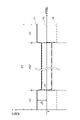
上部電極30は、遮蔽構造を有する。遮蔽構造は、ガス吐出孔34aから電極プレート34とガスプレート36との間へ移動するラジカル又はガスを遮蔽する構造である。図6は、遮蔽構造の一例を示す部分拡大図である。図6は、図3の部分拡大図である。図6に示される遮蔽構造は、ガスプレート36の下面36cの突出部36g(接続部材の一例)である。つまり、図6の例では、ガスプレート36が遮蔽構造を有する。突出部36gは、ガス流路36aの下端360aの周囲を囲むように形成される。これにより、ガス流路36aの下端360aとガス吐出孔34aの上端340bとが、突出部36gの内部流路によって接続される。突出部36gは、電極プレート34の上面34bと密着するため、ガス吐出孔34aから電極プレート34とガスプレート36との間へ移動するラジカル又はガスを物理的に遮蔽することができる。
[Details of shielding structure]
The
遮蔽構造は、図6に示される例に限定されず、種々の態様で実現される。図7は、遮蔽構造の他の例を示す部分拡大図である。図7に示されるように、遮蔽構造は、電極プレート34とガスプレート36との間に介在し、ガス吐出孔34aの上端とガス流路36aの下端とを接続する接続部材360g(接続部材の一例)を有する。この接続部材360gは、図6に示される突出部36gに相当する部材であり、ガスプレート36及び電極プレート34とは別体で構成される。接続部材360gは、その上端がガスプレート36の下面の第2領域36fに接続され、その下端が電極プレート34の上面34bに接続される。接続部材360gは、その内部にガス吐出孔34aとガス流路36aとを連通する内部流路を画成する。接続部材360gは、ガスプレート36の下面の第2領域36fと電極プレート34の上面34bとに密着するため、ガス吐出孔34aから電極プレート34とガスプレート36との間へ移動するラジカル又はガスを物理的に遮蔽することができる。
The shielding structure is not limited to the example shown in FIG. 6 and can be realized in various ways. FIG. 7 is a partially enlarged view showing another example of the shielding structure. As shown in FIG. 7, the shielding structure is interposed between the
図8は、遮蔽構造の他の例を示す部分拡大図である。図8に示されるように、遮蔽構造は、電極プレート34の上面の突出部34g(接続部材の一例)であり、突出部34gは、図6に示される突出部36gに相当する。つまり、図8の例では、電極プレート34が遮蔽構造を有する。電極プレート34の突出部34gは、ガスプレート36の下面の第2領域36fと密着するため、ガス吐出孔34aから電極プレート34とガスプレート36との間へ移動するラジカル又はガスを物理的に遮蔽することができる。なお、接続部材は、突出部34gと突出部36gとの組合せから構成されてもよい。つまり、接続部材は、突出部36gに相当する上部材と、突出部34gに相当する下部材とを組み合わせて構成されてもよい。
FIG. 8 is a partially enlarged view showing another example of the shielding structure. As shown in FIG. 8, the shielding structure is a protruding
図9は、遮蔽構造の他の例を示す部分拡大図である。図9に示されるように、遮蔽構造は、ガスソース群41(ガス供給源の一例)と、ガスソース群41に接続される供給流路36hとを有する。ガスソース群41は、ガスソース群40と同様に構成され、複数のガス供給源を含み得る。複数のガス供給源の少なくとも1つは、遮蔽ガスを供給流路36hに供給する。供給流路36hは、ガスプレート36に形成され、一例として、ガスプレート36のガス流路36aの周囲を囲むように形成される。ガス流路36a及び供給流路36hの下端部分に対応するガスプレート36の下面36cは、下方に突出しており、突出部36jを構成する。突出部36jの下端面は、ガスプレート36の第2領域36fである。供給流路36hは、その下端がガスプレート36の下面36cの第2領域36fに位置する。第2領域36fと電極プレート34の上面34bとの間には隙間が形成され、空間Sを提供する。供給流路36hは、空間Sに遮蔽ガスを供給することにより、電極プレート34とガスプレート36との間へ移動するラジカル又はガスを遮蔽する。遮蔽ガスの成分は、ガスソース群40により供給される処理ガスの成分と同一とすることができる。遮蔽ガスの一例はアルゴンガスである。
FIG. 9 is a partially enlarged view showing another example of the shielding structure. As shown in FIG. 9 , the shielding structure has a gas source group 41 (an example of a gas supply source) and a
なお、図9に示される遮蔽構造においては、突出部36jは存在しなくてもよい。また、電極プレート34及びガスプレート36が接触していた場合、プラズマ生成時に接触部分の温度は500℃以上となる。この場合、電極プレート34及びガスプレート36の接触部分が変質するおそれがある。図9に示される遮蔽構造は、電極プレート34とガスプレート36とが非接触となる。このため、接触による変質を防止することができる。また、電極プレート34とガスプレート36との熱膨張差に起因する摩擦や摩耗により、パーティクルが発生することを抑制することができる。
It should be noted that the
図10は、遮蔽構造の他の例を示す部分拡大図である。図10に示されるように、遮蔽構造は、排気装置51と、排気装置51に接続される排気流路36kとを有する。排気装置51は、減圧可能な装置であり、一例として真空ポンプである。排気流路36kは、ガスプレート36に形成され、一例として、ガスプレート36のガス流路36aの周囲を囲むように形成される。ガス流路36a及び排気流路36kの下端部分に対応するガスプレート36の下面36cは、下方に突出しており、突出部36jを構成する。突出部36jの下端面は、ガスプレート36の第2領域36fである。排気流路36kは、その下端がガスプレート36の下面36cの第2領域36fに位置する。第2領域36fと電極プレート34の上面34bとの間には隙間が形成され、空間Sを提供する。排気装置51は、排気流路36kを介して空間Sを減圧することにより、電極プレート34とガスプレート36との間へ移動するラジカル又はガスを遮蔽する。
FIG. 10 is a partially enlarged view showing another example of the shielding structure. As shown in FIG. 10 , the shielding structure has an
なお、図10に示される遮蔽構造においては、突出部36jは存在しなくてもよい。図10に示される遮蔽構造は、図9に示される遮蔽構造と同様に、電極プレート34とガスプレート36とが非接触となる。このため、接触による変質を防止することができる。また、電極プレート34とガスプレート36との熱膨張差に起因する摩擦や摩耗により、パーティクルが発生することを抑制することができる。
In addition, in the shielding structure shown in FIG. 10, the projecting
図11は、遮蔽構造の他の例を示す部分拡大図である。電極プレート34とガスプレート36との接触界面に変質を防止するための処理が施されていてもよい。一例として、図11に示されるように、ガスプレート36は、少なくとも電極プレート34との接触箇所に、不働態層36mを有していてもよい。これにより、接触による変質を防止することができる。例えば、ガスプレート36を形成する材料がシリコンであり、電極プレート34を形成する材料が金属である場合、ガスプレート36と電極プレート34との接触箇所においてシリサイドが形成されるおそれがある。不働態層36mは、接触箇所がシリサイドに変質することを防止することができる。さらに、遮蔽構造が不働態層36mを備えることにより、クリーニング処理で除去することが困難なパーティクルの発生を抑制することができる。このようなパーティクルの一例は、フッ化アルミニウムである。
FIG. 11 is a partially enlarged view showing another example of the shielding structure. The contact interface between the
[組立て方法]
図12は、一つの例示的実施形態に係る方法を概略的に示す図である。図12に示される方法は、上部電極構造を組み立てる方法である。この方法は、接合工程(ステップS10)、位置決め工程(ステップS12)、及び、取付工程(ステップS14)を有する。
[Assembly method]
FIG. 12 schematically illustrates a method according to one exemplary embodiment. The method shown in FIG. 12 is a method of assembling the upper electrode structure. This method has a bonding step (step S10), a positioning step (step S12), and a mounting step (step S14).
最初に、接合工程(ステップS10)が実施される。この工程では、ガスプレート36の下面36cの第1領域36eに静電チャック35の上面(接触面35c)を接合する。続いて、位置決め工程(ステップS12)では、以下の条件を満たすように電極プレート34の上面34bとガスプレート36の下面36cとを位置決めする。
First, a bonding step (step S10) is performed. In this step, the upper surface (
条件は、電極プレート34の上面34bとガスプレート36の下面36cの第2領域36fとの間に、静電チャック35よりも薄い接続部材が位置することを含む。接続部材は、例えば、図6の突出部36gであってもよいし、図7の接続部材360gであってもよいし、図8の突出部34gであってもよい。条件は、電極プレート34に形成されたガス吐出孔34aがガス流路36aと対向することを含む。例えば、ガス吐出孔34aとガス流路36aとが同軸となるように配置される。条件は、電極プレート34の上面34bが静電チャック35の下面(吸着面35d)に接触することを含む。
The conditions include that a connecting member thinner than the
続いて、取付工程(ステップS14)では、位置決めされた電極プレート34を支持する部材32をガスプレート36に取り付ける。以上で上部電極30が完成する。静電チャック35により電極プレート34が吸着されてガスプレート36に押し当てられたときに、静電チャック35は、電極プレート34の上面34bとガスプレート36の下面36cとの間で圧縮される。これにより、電極プレート34の上面34bが接続部材に突き当たるため、高さ方向(厚さ方向)の位置決めをすることができる。このため、取り付け高さ精度が向上し、結果として電極プレート34の温度調整の精度が低下することを抑制することができる。
Subsequently, in the mounting step (step S14), the
[静電チャックの制御方法]
静電チャック35は、図4及び図5に示されるように、第1電極351と第2電極350とを有し得る。第1直流電源39a及び第2直流電源39bは、極性を制御した電圧を電極へと印加する。図13は、双極方式の吸着の一例を説明する図である。図13に示されるように、静電チャック35の第1直流電源39aは、正の電圧を第1電極351へ印加する。第1電極351は、正に帯電する。静電チャック35の第2直流電源39bは、負の電圧を第2電極350へ印加する。第2電極350は、負に帯電する。プラズマPが生成されない場合には、第1電極351に対向する電極プレート34の一部は、負に帯電し、第2電極350に対向する電極プレート34の一部は、正に帯電する。このため、静電引力により、電極プレート34は保持される。一方、プラズマPが生成された場合、負の自己バイアスが電極プレート34に発生し、電極プレート34は負に帯電する。このように、双極方式は、プラズマPが生成されていない場合であっても吸着力を発生させることができる。
[Electrostatic Chuck Control Method]
The
図14は、単極方式の吸着の一例を説明する図である。図14に示されるように、静電チャック35の第1直流電源39aは、正の電圧を第1電極351へ印加する。第1電極351は、正に帯電する。また、静電チャック35の第2直流電源39bは、正の電圧を第2電極350へ印加する。第2電極350は、正に帯電する。このように、単極方式は、電荷の流入、つまり、プラズマPが生成されていないと、吸着力を発生させることができない。
FIG. 14 is a diagram illustrating an example of monopolar adsorption. As shown in FIG. 14, the first
制御部Cntは、第1直流電源39a及び第2直流電源39bを制御して吸着方式を切り換えることができる。
The controller Cnt can control the first
図15は、第1電極及び第2電極に印加される電圧と時間との関係の一例を示すグラフである。横軸は時間であり、縦軸は電圧である。図15には、プラズマ処理装置10によるプロセス期間PTが示されている。プロセス期間PTは、プラズマ生成期間PGTとアイドル期間ATとを交互に含む。プラズマ生成期間PGTは、プラズマ処理装置10によりプラズマが生成される期間である。アイドル期間ATでは、プラズマ処理装置10によりプラズマが生成されない期間である。
FIG. 15 is a graph showing an example of the relationship between the voltage applied to the first electrode and the second electrode and time. The horizontal axis is time and the vertical axis is voltage. FIG. 15 shows the process period PT by the
制御部Cntは、少なくともアイドル期間ATにおいて、静電チャック35の第1電極351及び第2電極350に対して互いに異なる極性の電圧を印加する。例えば、図15に示されるように、制御部Cntは、第1電極351に電圧パターンV1で示される電圧を印加し、第2電極350に電圧パターンV2で示される電圧を印加する。電圧パターンV1は、アイドル期間AT及びプラズマ生成期間PGTの何れの場合も正の極性を有する電圧となるパターンである。つまり、第1電極351には常に正の極性を有する電圧が印加される。一方、電圧パターンV2は、アイドル期間ATの場合には負の極性を有する電圧となり、プラズマ生成期間PGTの場合には正の極性を有する電圧となるパターンである。つまり、第2電極350には、アイドル期間ATに負の極性を有する電圧が印加され、プラズマ生成期間PGTに正の極性を有する電圧が印加される。なお、図15の電圧パターンV3は、直流電源部70によって電極プレート34に印加される電圧のパターンである。直流電源部70は、連続的に電圧を印加してもよいし、パルス状の電圧を印加してもよい。また、直流電源部70は備えていなくてもよい。
The controller Cnt applies voltages of different polarities to the
このように、制御部Cntは、アイドル期間ATにおいて、双極方式で電極プレート34を保持することで、温度制御されたガスプレート36に電極プレート34を吸着させることができる。これにより、プラズマから入熱が無いアイドル期間ATであっても電極プレート34を温度調整することにより、以降のプラズマ生成期間PGTにおける電極プレート34の温度調整を効率良く行うことができる。
In this manner, the control unit Cnt holds the
また、制御部Cntは、プラズマ生成期間PGTにおいて、第1電極351及び第2電極350それぞれに正の電圧を印加することで、単極方式で電極プレート34を保持する。これにより、プラズマ生成時に吸着力を低下させることなく、電極プレート34を保持し、温度調整することができる。
Further, the control unit Cnt applies a positive voltage to each of the
次に、制御部Cntによる他の制御方法を例示する。図16は、第1電極及び第2電極に印加される電圧と時間との関係の一例を示すグラフである。横軸は時間であり、縦軸は電圧である。図16には、プラズマ処理装置10によるプロセス期間PTが示されている。プロセス期間PTは、プラズマ生成期間PGTとアイドル期間ATとを交互に含む。
Next, another control method by the control unit Cnt will be exemplified. FIG. 16 is a graph showing an example of the relationship between the voltage applied to the first electrode and the second electrode and time. The horizontal axis is time and the vertical axis is voltage. FIG. 16 shows the process period PT by the
図16に示される電圧パターンV1は、最初のアイドル期間ATでは正の電圧であり、次のアイドル期間ATでは負の電圧であり、その次のアイドル期間ATでは正の電圧となる。プラズマ生成期間PGTは常に正の電圧である。一方、電圧パターンV2は、最初のアイドル期間ATでは負の電圧であり、次のアイドル期間ATでは正の電圧であり、その次のアイドル期間ATでは負の電圧となる。プラズマ生成期間PGTは常に正の電圧である。このように、第1電極351及び第2電極350それぞれに印加される電圧の極性がアイドル期間ATの度に入れ替わる。このように電圧を印加することにより、電極の極性が一つに固定されないため、一方向へ電荷が移動すること(マイグレーション)を回避することができる。これにより、吸着力が減少することを回避することができる。
The voltage pattern V1 shown in FIG. 16 has a positive voltage in the first idle period AT, a negative voltage in the next idle period AT, and a positive voltage in the next idle period AT. The plasma generation period PGT is always a positive voltage. On the other hand, the voltage pattern V2 has a negative voltage in the first idle period AT, a positive voltage in the next idle period AT, and a negative voltage in the next idle period AT. The plasma generation period PGT is always a positive voltage. Thus, the polarities of the voltages applied to the
図17は、第1電極及び第2電極に印加される電圧と時間との関係の一例を示すグラフである。横軸は時間であり、縦軸は電圧である。図17には、プラズマ処理装置10によるプロセス期間PTが示されている。プロセス期間PTは、プラズマ生成期間PGTとアイドル期間ATとを交互に含む。制御部Cntは、第1電極351に電圧パターンV1で示される電圧を印加し、第2電極350に電圧パターンV2で示される電圧を印加する。図17に示される電圧パターンV1は、図15に示される電圧パターンV1と比較して、プロセス期間PT全体を通して正の電圧である点は同一であるものの、プラズマ生成期間PGTの正の大きさが異なる。具体的には、アイドル期間ATにおいて第1電極351に印加される正の電圧と電極プレート34に印加される電圧との実効的な差分ΔVが、プロセス期間PT全体を通して一定になるように、電圧パターンV1を変更してもよい。同様に、図17に示される電圧パターンV2は、図15に示される電圧パターンV2と比較して、正負の極性は同一であるものの、プラズマ生成期間PGTの正の大きさが異なる。具体的には、アイドル期間ATにおいて第1電極351に印加される正の電圧と電極プレート34に印加される電圧との実効的な差分ΔVが常に一定になるように、電圧パターンV2が変更される。なお、図中では、電極プレート34に発生する負の自己バイアスが電圧パターンV3で示される電圧よりも小さい場合を図示している。電極プレート34に発生する負の自己バイアスが電圧パターンV3で示される電圧以上である場合には、負の自己バイアスを基準として実効的な差分ΔVを算出し、電圧パターンV1,V2が変更される。
FIG. 17 is a graph showing an example of the relationship between the voltage applied to the first electrode and the second electrode and time. The horizontal axis is time and the vertical axis is voltage. FIG. 17 shows the process period PT by the
以上、種々の例示的実施形態について説明してきたが、上述した例示的実施形態に限定されることなく、様々な省略、置換、及び変更がなされてもよい。また、異なる実施形態における要素を組み合わせて他の実施形態を形成することが可能である。 While various exemplary embodiments have been described above, various omissions, substitutions, and modifications may be made without being limited to the exemplary embodiments described above. Also, elements from different embodiments can be combined to form other embodiments.
例えば、プラズマ処理装置10は、容量結合型のプラズマ処理装置であるが、別の実施形態に係るプラズマ処理装置は、異なるタイプのプラズマ処理装置であってもよい。そのようなプラズマ処理装置は、任意のタイプのプラズマ処理装置であり得る。そのようなプラズマ処理装置としては、誘導結合型のプラズマ処理装置、マイクロ波といった表面波によってプラズマを生成するプラズマ処理装置が例示される。
For example, the
また、プラズマ処理装置10は、下部電極18に2系統の高周波電源が接続され、上部電極30に直流電源が接続される例を示したが、これに限定されない。例えば、プラズマ処理装置10は、上部電極30は備えていなくてもよい。例えば、プラズマ処理装置10は、下部電極18及び上部電極30に高周波電源が接続されてもよい。
Moreover, although the
以上の説明から、本開示の種々の実施形態は、説明の目的で本明細書で説明されており、本開示の範囲及び主旨から逸脱することなく種々の変更をなし得ることが、理解されるであろう。したがって、本明細書に開示した種々の実施形態は限定することを意図しておらず、真の範囲と主旨は、添付の特許請求の範囲によって示される。 From the foregoing description, it will be appreciated that various embodiments of the present disclosure have been set forth herein for purposes of illustration, and that various changes may be made without departing from the scope and spirit of the present disclosure. Will. Therefore, the various embodiments disclosed herein are not intended to be limiting, with a true scope and spirit being indicated by the following claims.
10…プラズマ処理装置、34…電極プレート、34a…ガス吐出孔、35…静電チャック(静電吸着部の一例)、36…ガスプレート、36a…ガス流路、37…冷却プレート、41…ガスソース群(ガス供給源の一例)、51…排気装置、Cnt…制御部。
DESCRIPTION OF
Claims (14)
第1貫通孔を有する電極プレートと、
前記電極プレート上に配置され、部品孔を有する静電吸着部と、
前記静電吸着部の前記部品孔内に配置され、前記第1貫通孔と連通する第2貫通孔を有する遮蔽部品と、
前記静電吸着部及び前記遮蔽部品の上に配置され、前記第2貫通孔と連通する第3貫通孔を有するガスプレートと
を備え、
前記遮蔽部品は、前記第1貫通孔、前記第2貫通孔及び前記第3貫通孔内を移動する流動性の物質が前記静電吸着部に接触することを阻止するように、前記部品孔内で前記電極プレートから前記ガスプレートまで延在している、
上部電極構造。 An upper electrode structure of a plasma processing apparatus,
an electrode plate having a first through hole;
an electrostatic adsorption part disposed on the electrode plate and having a component hole;
a shielding component disposed in the component hole of the electrostatic attraction part and having a second through hole communicating with the first through hole;
a gas plate disposed on the electrostatic adsorption portion and the shielding component and having a third through hole communicating with the second through hole ;
The shielding component is arranged inside the component hole so as to prevent a fluid substance moving in the first through hole, the second through hole, and the third through hole from coming into contact with the electrostatic attraction section. extending from the electrode plate to the gas plate at
Upper electrode structure.
弾性を有する誘電体からなる第1本体部と、前記第1本体部の内部に配置された第1電極とを有する第1吸着部と、
弾性を有する誘電体からなる第2本体部と、前記第2本体部の内部に配置された第2電極とを有する第2吸着部と、
を有し、
前記第1電極及び前記第2電極には、互いに異なる極性の電圧が印加される、請求項1に記載の上部電極構造。 The electrostatic attraction part is
a first adsorption part having a first main body made of an elastic dielectric and a first electrode arranged inside the first main body;
a second adsorption part having a second main body made of an elastic dielectric and a second electrode arranged inside the second main body;
has
2. The upper electrode structure of claim 1 , wherein voltages having different polarities are applied to the first electrode and the second electrode.
弾性を有する誘電体からなる第1本体部と、前記第1本体部の内部に配置された第1電極とを有する第1吸着部と、
弾性を有する誘電体からなる第2本体部と、前記第2本体部の内部に配置された第2電極とを有する第2吸着部と、
を有し、
前記第1電極及び前記第2電極には、同一の極性の電圧が印加される、請求項1に記載の上部電極構造。 The electrostatic attraction part is
a first adsorption part having a first main body made of an elastic dielectric and a first electrode arranged inside the first main body;
a second adsorption part having a second main body made of an elastic dielectric and a second electrode arranged inside the second main body;
has
2. The upper electrode structure of claim 1 , wherein voltages of the same polarity are applied to the first electrode and the second electrode.
前記プラズマ処理チャンバ内に配置され、下部電極を有する基板支持器と、
前記下部電極の上方に配置された上部電極構造と、
を備え、
前記上部電極構造は、
第1貫通孔を有する電極プレートと、
前記電極プレート上に配置され、部品孔を有する静電吸着部と、
前記静電吸着部の前記部品孔内に配置され、前記第1貫通孔と連通する第2貫通孔を有する遮蔽部品と、
前記静電吸着部及び前記遮蔽部品の上に配置され、前記第2貫通孔と連通する第3貫通孔を有するガスプレートと
を有し、
前記遮蔽部品は、前記第1貫通孔、前記第2貫通孔及び前記第3貫通孔内を移動する流動性の物質が前記静電吸着部に接触することを阻止するように、前記部品孔内で前記電極プレートから前記ガスプレートまで延在している、
プラズマ処理装置。 a plasma processing chamber;
a substrate support disposed within the plasma processing chamber and having a lower electrode;
an upper electrode structure disposed above the lower electrode;
with
The upper electrode structure is
an electrode plate having a first through hole;
an electrostatic adsorption part disposed on the electrode plate and having a component hole;
a shielding component disposed in the component hole of the electrostatic attraction part and having a second through hole communicating with the first through hole;
a gas plate disposed on the electrostatic adsorption portion and the shielding component and having a third through hole communicating with the second through hole ;
The shielding component is arranged inside the component hole so as to prevent a fluid substance moving in the first through hole, the second through hole, and the third through hole from coming into contact with the electrostatic attraction section. extending from the electrode plate to the gas plate at
Plasma processing equipment.
Priority Applications (5)
| Application Number | Priority Date | Filing Date | Title |
|---|---|---|---|
| JP2019006074A JP7153574B2 (en) | 2019-01-17 | 2019-01-17 | Top electrode structure, plasma processing apparatus, and method of assembling top electrode structure |
| KR1020200002434A KR20200089608A (en) | 2019-01-17 | 2020-01-08 | Upper electrode, plasma processing apparatus, and method of assembling upper electrode |
| CN202010020933.2A CN111446143A (en) | 2019-01-17 | 2020-01-09 | Top electrode structure, plasma processing apparatus and method of assembling top electrode structure |
| US16/738,369 US11443924B2 (en) | 2019-01-17 | 2020-01-09 | Upper electrode and plasma processing apparatus |
| TW109100728A TW202032618A (en) | 2019-01-17 | 2020-01-09 | Upper electrode, plasma processing apparatus, and method of assembling upper electrode |
Applications Claiming Priority (1)
| Application Number | Priority Date | Filing Date | Title |
|---|---|---|---|
| JP2019006074A JP7153574B2 (en) | 2019-01-17 | 2019-01-17 | Top electrode structure, plasma processing apparatus, and method of assembling top electrode structure |
Publications (3)
| Publication Number | Publication Date |
|---|---|
| JP2020115419A JP2020115419A (en) | 2020-07-30 |
| JP2020115419A5 JP2020115419A5 (en) | 2021-11-11 |
| JP7153574B2 true JP7153574B2 (en) | 2022-10-14 |
Family
ID=71608340
Family Applications (1)
| Application Number | Title | Priority Date | Filing Date |
|---|---|---|---|
| JP2019006074A Active JP7153574B2 (en) | 2019-01-17 | 2019-01-17 | Top electrode structure, plasma processing apparatus, and method of assembling top electrode structure |
Country Status (5)
| Country | Link |
|---|---|
| US (1) | US11443924B2 (en) |
| JP (1) | JP7153574B2 (en) |
| KR (1) | KR20200089608A (en) |
| CN (1) | CN111446143A (en) |
| TW (1) | TW202032618A (en) |
Families Citing this family (5)
| Publication number | Priority date | Publication date | Assignee | Title |
|---|---|---|---|---|
| JP7454407B2 (en) * | 2020-03-02 | 2024-03-22 | 東京エレクトロン株式会社 | Plasma treatment method and plasma treatment device |
| US20220093361A1 (en) * | 2020-09-22 | 2022-03-24 | Applied Materials, Inc. | Showerhead assembly with recursive gas channels |
| WO2022123615A1 (en) * | 2020-12-07 | 2022-06-16 | 東芝三菱電機産業システム株式会社 | Active gas generation device |
| WO2023058480A1 (en) * | 2021-10-05 | 2023-04-13 | 東京エレクトロン株式会社 | Upper electrode structure, and plasma processing device |
| CN114420526B (en) * | 2022-01-18 | 2023-09-12 | 江苏天芯微半导体设备有限公司 | Bush and wafer preprocessing device |
Citations (5)
| Publication number | Priority date | Publication date | Assignee | Title |
|---|---|---|---|---|
| JP2009301802A (en) | 2008-06-11 | 2009-12-24 | Tokyo Electron Ltd | Plasma processing apparatus |
| JP2011009249A (en) | 2009-06-23 | 2011-01-13 | Hitachi High-Technologies Corp | Plasma processing apparatus |
| JP2015216261A (en) | 2014-05-12 | 2015-12-03 | 東京エレクトロン株式会社 | Upper electrode structure of plasma processing device, plasma processing device, and method for operating plasma processing device |
| US20170352567A1 (en) | 2016-06-07 | 2017-12-07 | Applied Materials, Inc. | High power electrostatic chuck design with radio frequency coupling |
| JP2018056248A (en) | 2016-09-28 | 2018-04-05 | 株式会社日立ハイテクノロジーズ | Operational method of plasma processing apparatus |
Family Cites Families (6)
| Publication number | Priority date | Publication date | Assignee | Title |
|---|---|---|---|---|
| US5572398A (en) * | 1994-11-14 | 1996-11-05 | Hewlett-Packard Co. | Tri-polar electrostatic chuck |
| TW492135B (en) * | 2000-05-25 | 2002-06-21 | Tomoegawa Paper Co Ltd | Adhesive sheets for static electricity chuck device, and static electricity chuck device |
| JP5186504B2 (en) * | 2007-09-06 | 2013-04-17 | 株式会社クリエイティブ テクノロジー | Method for manufacturing gas supply structure in electrostatic chuck device, gas supply structure for electrostatic chuck device, and electrostatic chuck device |
| JP2010182763A (en) * | 2009-02-04 | 2010-08-19 | Hitachi High-Technologies Corp | Plasma processing apparatus |
| US9449859B2 (en) * | 2009-10-09 | 2016-09-20 | Applied Materials, Inc. | Multi-gas centrally cooled showerhead design |
| JP7073098B2 (en) * | 2017-12-27 | 2022-05-23 | 株式会社日立ハイテク | Wafer processing method and wafer processing equipment |
-
2019
- 2019-01-17 JP JP2019006074A patent/JP7153574B2/en active Active
-
2020
- 2020-01-08 KR KR1020200002434A patent/KR20200089608A/en unknown
- 2020-01-09 TW TW109100728A patent/TW202032618A/en unknown
- 2020-01-09 US US16/738,369 patent/US11443924B2/en active Active
- 2020-01-09 CN CN202010020933.2A patent/CN111446143A/en active Pending
Patent Citations (5)
| Publication number | Priority date | Publication date | Assignee | Title |
|---|---|---|---|---|
| JP2009301802A (en) | 2008-06-11 | 2009-12-24 | Tokyo Electron Ltd | Plasma processing apparatus |
| JP2011009249A (en) | 2009-06-23 | 2011-01-13 | Hitachi High-Technologies Corp | Plasma processing apparatus |
| JP2015216261A (en) | 2014-05-12 | 2015-12-03 | 東京エレクトロン株式会社 | Upper electrode structure of plasma processing device, plasma processing device, and method for operating plasma processing device |
| US20170352567A1 (en) | 2016-06-07 | 2017-12-07 | Applied Materials, Inc. | High power electrostatic chuck design with radio frequency coupling |
| JP2018056248A (en) | 2016-09-28 | 2018-04-05 | 株式会社日立ハイテクノロジーズ | Operational method of plasma processing apparatus |
Also Published As
| Publication number | Publication date |
|---|---|
| CN111446143A (en) | 2020-07-24 |
| JP2020115419A (en) | 2020-07-30 |
| TW202032618A (en) | 2020-09-01 |
| KR20200089608A (en) | 2020-07-27 |
| US20200234930A1 (en) | 2020-07-23 |
| US11443924B2 (en) | 2022-09-13 |
Similar Documents
| Publication | Publication Date | Title |
|---|---|---|
| JP7153574B2 (en) | Top electrode structure, plasma processing apparatus, and method of assembling top electrode structure | |
| KR101677239B1 (en) | Plasma processing apparatus and plasma processing method | |
| KR100886982B1 (en) | Plasma processing apparatus and plasma processing method | |
| KR20140094475A (en) | Mounting table and plasma processing apparatus | |
| JP5702968B2 (en) | Plasma processing apparatus and plasma control method | |
| JP2007005491A (en) | Electrode assembly and plasma processing apparatus | |
| KR102302313B1 (en) | Method of adsorbing target object on mounting table and plasma processing apparatus | |
| KR101835435B1 (en) | Plasma processing apparatus | |
| JP2019149422A (en) | Plasma processing apparatus and mounting table manufacturing method | |
| WO2019244631A1 (en) | Stage and substrate processing apparatus | |
| US20220093407A1 (en) | Method for Controlling Electrostatic Attractor and Plasma Processing Apparatus | |
| US20220336193A1 (en) | Plasma processing apparatus and plasma processing method | |
| TW202141563A (en) | Plasma processing apparatus | |
| JP4709047B2 (en) | Substrate processing apparatus and side wall parts | |
| TW202117913A (en) | Substrate support and plasma processing apparatus | |
| TW201535511A (en) | Plasma processing device | |
| KR20220030173A (en) | Stage and plasma processing apparatus | |
| CN111446144B (en) | Control method of electrostatic adsorption part and plasma processing device | |
| JP2022007865A (en) | Etching device and etching method | |
| JP2022028461A (en) | Cleaning method of plasma processing device and plasma processing device | |
| JP7454407B2 (en) | Plasma treatment method and plasma treatment device | |
| WO2023058480A1 (en) | Upper electrode structure, and plasma processing device | |
| JP2023031716A (en) | Plasma processing device | |
| TW202341344A (en) | Substrate support and plasma processing apparatus |
Legal Events
| Date | Code | Title | Description |
|---|---|---|---|
| A521 | Request for written amendment filed |
Free format text: JAPANESE INTERMEDIATE CODE: A523 Effective date: 20210930 |
|
| A621 | Written request for application examination |
Free format text: JAPANESE INTERMEDIATE CODE: A621 Effective date: 20210930 |
|
| A131 | Notification of reasons for refusal |
Free format text: JAPANESE INTERMEDIATE CODE: A131 Effective date: 20220628 |
|
| A977 | Report on retrieval |
Free format text: JAPANESE INTERMEDIATE CODE: A971007 Effective date: 20220629 |
|
| A521 | Request for written amendment filed |
Free format text: JAPANESE INTERMEDIATE CODE: A523 Effective date: 20220826 |
|
| TRDD | Decision of grant or rejection written | ||
| A01 | Written decision to grant a patent or to grant a registration (utility model) |
Free format text: JAPANESE INTERMEDIATE CODE: A01 Effective date: 20220906 |
|
| A61 | First payment of annual fees (during grant procedure) |
Free format text: JAPANESE INTERMEDIATE CODE: A61 Effective date: 20221003 |
|
| R150 | Certificate of patent or registration of utility model |
Ref document number: 7153574 Country of ref document: JP Free format text: JAPANESE INTERMEDIATE CODE: R150 |