JP7148337B2 - Position sensing apparatus, lithographic apparatus, force sensor and apparatus with force sensor - Google Patents
Position sensing apparatus, lithographic apparatus, force sensor and apparatus with force sensor Download PDFInfo
- Publication number
- JP7148337B2 JP7148337B2 JP2018172821A JP2018172821A JP7148337B2 JP 7148337 B2 JP7148337 B2 JP 7148337B2 JP 2018172821 A JP2018172821 A JP 2018172821A JP 2018172821 A JP2018172821 A JP 2018172821A JP 7148337 B2 JP7148337 B2 JP 7148337B2
- Authority
- JP
- Japan
- Prior art keywords
- spatial frequency
- grating
- scale
- light
- light receiving
- Prior art date
- Legal status (The legal status is an assumption and is not a legal conclusion. Google has not performed a legal analysis and makes no representation as to the accuracy of the status listed.)
- Active
Links
- 238000001514 detection method Methods 0.000 claims description 56
- 230000003287 optical effect Effects 0.000 claims description 37
- 238000012545 processing Methods 0.000 claims description 25
- 230000004044 response Effects 0.000 claims description 25
- 238000006073 displacement reaction Methods 0.000 claims description 21
- 239000000758 substrate Substances 0.000 claims description 12
- 238000000034 method Methods 0.000 claims description 6
- 230000008569 process Effects 0.000 claims description 4
- 238000013459 approach Methods 0.000 claims description 2
- 238000000059 patterning Methods 0.000 claims description 2
- 238000009826 distribution Methods 0.000 description 22
- 238000010586 diagram Methods 0.000 description 20
- 239000011295 pitch Substances 0.000 description 17
- 238000000926 separation method Methods 0.000 description 10
- 238000004519 manufacturing process Methods 0.000 description 7
- 230000000737 periodic effect Effects 0.000 description 6
- 238000004364 calculation method Methods 0.000 description 5
- 230000005540 biological transmission Effects 0.000 description 4
- 230000000694 effects Effects 0.000 description 4
- 239000004065 semiconductor Substances 0.000 description 4
- 238000012935 Averaging Methods 0.000 description 2
- VYZAMTAEIAYCRO-UHFFFAOYSA-N Chromium Chemical compound [Cr] VYZAMTAEIAYCRO-UHFFFAOYSA-N 0.000 description 2
- 230000008859 change Effects 0.000 description 2
- 229910052804 chromium Inorganic materials 0.000 description 2
- 239000011651 chromium Substances 0.000 description 2
- 239000006059 cover glass Substances 0.000 description 2
- 230000008021 deposition Effects 0.000 description 2
- 238000005530 etching Methods 0.000 description 2
- 230000004907 flux Effects 0.000 description 2
- 239000004973 liquid crystal related substance Substances 0.000 description 2
- 238000001459 lithography Methods 0.000 description 2
- 238000003860 storage Methods 0.000 description 2
- WGLPBDUCMAPZCE-UHFFFAOYSA-N Trioxochromium Chemical compound O=[Cr](=O)=O WGLPBDUCMAPZCE-UHFFFAOYSA-N 0.000 description 1
- XAGFODPZIPBFFR-UHFFFAOYSA-N aluminium Chemical compound [Al] XAGFODPZIPBFFR-UHFFFAOYSA-N 0.000 description 1
- 229910052782 aluminium Inorganic materials 0.000 description 1
- 238000003491 array Methods 0.000 description 1
- 230000002238 attenuated effect Effects 0.000 description 1
- 238000006243 chemical reaction Methods 0.000 description 1
- 239000003795 chemical substances by application Substances 0.000 description 1
- 229910000423 chromium oxide Inorganic materials 0.000 description 1
- 238000007796 conventional method Methods 0.000 description 1
- 230000006866 deterioration Effects 0.000 description 1
- 230000008034 disappearance Effects 0.000 description 1
- 238000005516 engineering process Methods 0.000 description 1
- 238000012986 modification Methods 0.000 description 1
- 230000004048 modification Effects 0.000 description 1
- 230000003647 oxidation Effects 0.000 description 1
- 238000007254 oxidation reaction Methods 0.000 description 1
- 238000004806 packaging method and process Methods 0.000 description 1
- 239000010453 quartz Substances 0.000 description 1
- 230000009467 reduction Effects 0.000 description 1
- 239000011347 resin Substances 0.000 description 1
- 229920005989 resin Polymers 0.000 description 1
- 230000004043 responsiveness Effects 0.000 description 1
- VYPSYNLAJGMNEJ-UHFFFAOYSA-N silicon dioxide Inorganic materials O=[Si]=O VYPSYNLAJGMNEJ-UHFFFAOYSA-N 0.000 description 1
- 230000000087 stabilizing effect Effects 0.000 description 1
- 238000012546 transfer Methods 0.000 description 1
Images


Classifications
-
- G—PHYSICS
- G01—MEASURING; TESTING
- G01D—MEASURING NOT SPECIALLY ADAPTED FOR A SPECIFIC VARIABLE; ARRANGEMENTS FOR MEASURING TWO OR MORE VARIABLES NOT COVERED IN A SINGLE OTHER SUBCLASS; TARIFF METERING APPARATUS; MEASURING OR TESTING NOT OTHERWISE PROVIDED FOR
- G01D5/00—Mechanical means for transferring the output of a sensing member; Means for converting the output of a sensing member to another variable where the form or nature of the sensing member does not constrain the means for converting; Transducers not specially adapted for a specific variable
- G01D5/26—Mechanical means for transferring the output of a sensing member; Means for converting the output of a sensing member to another variable where the form or nature of the sensing member does not constrain the means for converting; Transducers not specially adapted for a specific variable characterised by optical transfer means, i.e. using infrared, visible, or ultraviolet light
- G01D5/32—Mechanical means for transferring the output of a sensing member; Means for converting the output of a sensing member to another variable where the form or nature of the sensing member does not constrain the means for converting; Transducers not specially adapted for a specific variable characterised by optical transfer means, i.e. using infrared, visible, or ultraviolet light with attenuation or whole or partial obturation of beams of light
- G01D5/34—Mechanical means for transferring the output of a sensing member; Means for converting the output of a sensing member to another variable where the form or nature of the sensing member does not constrain the means for converting; Transducers not specially adapted for a specific variable characterised by optical transfer means, i.e. using infrared, visible, or ultraviolet light with attenuation or whole or partial obturation of beams of light the beams of light being detected by photocells
- G01D5/347—Mechanical means for transferring the output of a sensing member; Means for converting the output of a sensing member to another variable where the form or nature of the sensing member does not constrain the means for converting; Transducers not specially adapted for a specific variable characterised by optical transfer means, i.e. using infrared, visible, or ultraviolet light with attenuation or whole or partial obturation of beams of light the beams of light being detected by photocells using displacement encoding scales
- G01D5/34746—Linear encoders
-
- G—PHYSICS
- G01—MEASURING; TESTING
- G01D—MEASURING NOT SPECIALLY ADAPTED FOR A SPECIFIC VARIABLE; ARRANGEMENTS FOR MEASURING TWO OR MORE VARIABLES NOT COVERED IN A SINGLE OTHER SUBCLASS; TARIFF METERING APPARATUS; MEASURING OR TESTING NOT OTHERWISE PROVIDED FOR
- G01D5/00—Mechanical means for transferring the output of a sensing member; Means for converting the output of a sensing member to another variable where the form or nature of the sensing member does not constrain the means for converting; Transducers not specially adapted for a specific variable
- G01D5/26—Mechanical means for transferring the output of a sensing member; Means for converting the output of a sensing member to another variable where the form or nature of the sensing member does not constrain the means for converting; Transducers not specially adapted for a specific variable characterised by optical transfer means, i.e. using infrared, visible, or ultraviolet light
- G01D5/32—Mechanical means for transferring the output of a sensing member; Means for converting the output of a sensing member to another variable where the form or nature of the sensing member does not constrain the means for converting; Transducers not specially adapted for a specific variable characterised by optical transfer means, i.e. using infrared, visible, or ultraviolet light with attenuation or whole or partial obturation of beams of light
- G01D5/34—Mechanical means for transferring the output of a sensing member; Means for converting the output of a sensing member to another variable where the form or nature of the sensing member does not constrain the means for converting; Transducers not specially adapted for a specific variable characterised by optical transfer means, i.e. using infrared, visible, or ultraviolet light with attenuation or whole or partial obturation of beams of light the beams of light being detected by photocells
- G01D5/347—Mechanical means for transferring the output of a sensing member; Means for converting the output of a sensing member to another variable where the form or nature of the sensing member does not constrain the means for converting; Transducers not specially adapted for a specific variable characterised by optical transfer means, i.e. using infrared, visible, or ultraviolet light with attenuation or whole or partial obturation of beams of light the beams of light being detected by photocells using displacement encoding scales
- G01D5/34707—Scales; Discs, e.g. fixation, fabrication, compensation
- G01D5/34715—Scale reading or illumination devices
-
- G—PHYSICS
- G01—MEASURING; TESTING
- G01D—MEASURING NOT SPECIALLY ADAPTED FOR A SPECIFIC VARIABLE; ARRANGEMENTS FOR MEASURING TWO OR MORE VARIABLES NOT COVERED IN A SINGLE OTHER SUBCLASS; TARIFF METERING APPARATUS; MEASURING OR TESTING NOT OTHERWISE PROVIDED FOR
- G01D5/00—Mechanical means for transferring the output of a sensing member; Means for converting the output of a sensing member to another variable where the form or nature of the sensing member does not constrain the means for converting; Transducers not specially adapted for a specific variable
- G01D5/26—Mechanical means for transferring the output of a sensing member; Means for converting the output of a sensing member to another variable where the form or nature of the sensing member does not constrain the means for converting; Transducers not specially adapted for a specific variable characterised by optical transfer means, i.e. using infrared, visible, or ultraviolet light
- G01D5/32—Mechanical means for transferring the output of a sensing member; Means for converting the output of a sensing member to another variable where the form or nature of the sensing member does not constrain the means for converting; Transducers not specially adapted for a specific variable characterised by optical transfer means, i.e. using infrared, visible, or ultraviolet light with attenuation or whole or partial obturation of beams of light
- G01D5/34—Mechanical means for transferring the output of a sensing member; Means for converting the output of a sensing member to another variable where the form or nature of the sensing member does not constrain the means for converting; Transducers not specially adapted for a specific variable characterised by optical transfer means, i.e. using infrared, visible, or ultraviolet light with attenuation or whole or partial obturation of beams of light the beams of light being detected by photocells
- G01D5/347—Mechanical means for transferring the output of a sensing member; Means for converting the output of a sensing member to another variable where the form or nature of the sensing member does not constrain the means for converting; Transducers not specially adapted for a specific variable characterised by optical transfer means, i.e. using infrared, visible, or ultraviolet light with attenuation or whole or partial obturation of beams of light the beams of light being detected by photocells using displacement encoding scales
- G01D5/34776—Absolute encoders with analogue or digital scales
-
- G—PHYSICS
- G01—MEASURING; TESTING
- G01D—MEASURING NOT SPECIALLY ADAPTED FOR A SPECIFIC VARIABLE; ARRANGEMENTS FOR MEASURING TWO OR MORE VARIABLES NOT COVERED IN A SINGLE OTHER SUBCLASS; TARIFF METERING APPARATUS; MEASURING OR TESTING NOT OTHERWISE PROVIDED FOR
- G01D5/00—Mechanical means for transferring the output of a sensing member; Means for converting the output of a sensing member to another variable where the form or nature of the sensing member does not constrain the means for converting; Transducers not specially adapted for a specific variable
- G01D5/26—Mechanical means for transferring the output of a sensing member; Means for converting the output of a sensing member to another variable where the form or nature of the sensing member does not constrain the means for converting; Transducers not specially adapted for a specific variable characterised by optical transfer means, i.e. using infrared, visible, or ultraviolet light
- G01D5/32—Mechanical means for transferring the output of a sensing member; Means for converting the output of a sensing member to another variable where the form or nature of the sensing member does not constrain the means for converting; Transducers not specially adapted for a specific variable characterised by optical transfer means, i.e. using infrared, visible, or ultraviolet light with attenuation or whole or partial obturation of beams of light
- G01D5/34—Mechanical means for transferring the output of a sensing member; Means for converting the output of a sensing member to another variable where the form or nature of the sensing member does not constrain the means for converting; Transducers not specially adapted for a specific variable characterised by optical transfer means, i.e. using infrared, visible, or ultraviolet light with attenuation or whole or partial obturation of beams of light the beams of light being detected by photocells
- G01D5/36—Forming the light into pulses
- G01D5/38—Forming the light into pulses by diffraction gratings
Description
本発明は、位置検出装置、リソグラフィ装置、力覚センサ及び力覚センサを有する装置に関する。 The present invention relates to a position sensing device, a lithographic apparatus, a force sensor and an apparatus comprising a force sensor.
光学式位置検出装置においては、受光素子アレイの配列接続を切り替えることで、互いに異なる周期を有する複数のスケールパターンから、特定の周期成分のみを分離して検出することが可能な装置が提案されている(特許文献1参照)。このような光学式位置検出装置は、低分解能で絶対値特定範囲が広い信号と、高分解能で絶対値特定範囲が狭い信号とを動的に切り替えることができる。 As an optical position detection device, a device has been proposed that can separate and detect only a specific periodic component from a plurality of scale patterns having mutually different cycles by switching the arrangement connection of the light-receiving element array. (See Patent Document 1). Such an optical position detection device can dynamically switch between a low-resolution signal with a wide absolute value specification range and a high-resolution signal with a narrow absolute value specification range.
しかしながら、光学式位置検出装置では、分解能の比率が大きくなると、受光素子アレイを構成する受光素子の数が増大し、分離帯構造における効率低下や接合容量の増大などを招いてしまう。このような特性の低下は、光学式位置検出装置による位置の検出精度を低下させるおそれがある。 However, in the optical position detection device, as the resolution ratio increases, the number of light receiving elements constituting the light receiving element array increases, resulting in a decrease in efficiency and an increase in junction capacitance in the separation band structure. Such deterioration in characteristics may reduce the accuracy of position detection by the optical position detection device.
本発明は、このような従来技術の課題に鑑みてなされ、対象物の位置を異なる分解能で高精度に検出するのに有利な位置検出装置を提供することを例示的目的とする。 SUMMARY OF THE INVENTION It is an exemplary object of the present invention to provide a position detecting device that is advantageous in detecting the position of an object with different resolutions and with high accuracy.
上記目的を達成するために、本発明の一側面としての位置検出装置は、いずれか一方が対象物に設けられるスケール及び検出器を備え、前記スケールからの光を前記検出器で検出することで前記対象物の位置を検出する位置検出装置であって、前記スケールは、前記スケールと前記検出器との相対移動方向に第1空間周波数を有する第1格子パターンと、前記相対移動方向に前記第1空間周波数より低い第2空間周波数を有する第2格子パターンと、を含み、前記第2格子パターンのピッチは、前記第1格子パターンのピッチの8倍以上であり、前記検出器は、前記相対移動方向に沿って配置された複数の受光素子を含み、前記位置検出装置は、前記スケールと前記検出器との間に設けられ、前記相対移動方向に前記第1格子パターンからの干渉像の空間周波数から予め定められた周波数オフセット量だけオフセットさせた第3空間周波数を有する光学格子と、第1分解能モードでは、前記第1格子パターン及び前記光学格子を通過した光から前記周波数オフセット量に対応する空間周波数より低い第4空間周波数の成分の位相が検出されるように、前記第1分解能モードよりも分解能が低い第2分解能モードでは、前記第2格子パターン及び前記光学格子を通過した光から前記第2格子パターンの干渉像の空間周波数の成分の位相が検出されるように、前記複数の受光素子において出力を加算すべき、前記相対移動方向に連続した受光素子の数を設定する処理を行う処理部と、を有することを特徴とする。 In order to achieve the above object, a position detection device as one aspect of the present invention includes a scale and a detector, one of which is provided on an object, and detects light from the scale with the detector. In the position detection device for detecting the position of the object, the scale has a first grid pattern having a first spatial frequency in the direction of relative movement between the scale and the detector, and the first grid pattern in the direction of relative movement. a second grating pattern having a second spatial frequency lower than one spatial frequency, wherein the pitch of the second grating pattern is at least eight times the pitch of the first grating pattern; The position detection device includes a plurality of light receiving elements arranged along the direction of movement, the position detection device is provided between the scale and the detector, and detects a space of an interference image from the first grating pattern in the direction of relative movement. an optical grating having a third spatial frequency offset from frequency by a predetermined frequency offset amount; and a first resolution mode corresponding to the frequency offset amount from light passing through the first grating pattern and the optical grating. In the second resolution mode, which has a lower resolution than the first resolution mode, so that the phase of the component of the fourth spatial frequency lower than the spatial frequency is detected, from the light passing through the second grating pattern and the optical grating, the Performing a process of setting the number of light receiving elements continuous in the relative movement direction to which the outputs of the plurality of light receiving elements are to be added so that the phase of the spatial frequency component of the interference image of the second grating pattern is detected. and a processing unit.
本発明の更なる目的又はその他の側面は、以下、添付図面を参照して説明される好ましい実施形態によって明らかにされるであろう。 Further objects or other aspects of the present invention will be made clear by preferred embodiments described below with reference to the accompanying drawings.
本発明によれば、例えば、対象物の位置を異なる分解能で高精度に検出するのに有利な位置検出装置を提供することができる。 According to the present invention, for example, it is possible to provide a position detection device that is advantageous in detecting the position of an object with different resolutions with high accuracy.
以下、添付図面を参照して、本発明の好適な実施の形態について説明する。なお、各図において、同一の部材については同一の参照番号を付し、重複する説明は省略する。 Preferred embodiments of the present invention will be described below with reference to the accompanying drawings. In addition, in each figure, the same reference numerals are given to the same members, and redundant explanations are omitted.
<第1実施形態>
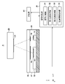
図1は、本発明の一側面としてのエンコーダ1の構成を示す概略図である。エンコーダ1は、いずれか一方が対象物に設けられるスケール及び検出器を備え、スケールからの光を検出器で検出することで対象物の位置を検出する光学式の位置検出装置である。
<First embodiment>
FIG. 1 is a schematic diagram showing the configuration of an
エンコーダ1は、位置検出の対象物である装置(不図示)の固定部に取り付けられるセンサユニット10と、かかる装置の可動部に取り付けられ、センサユニット10に対して可動部とともに移動可能なスケール20とを有するリニアエンコーダである。なお、装置の固定部にスケール20を取り付け、装置の可動部にセンサユニット10を取り付けてもよい。換言すれば、センサユニット10とスケール20とが相対移動可能であればよい。以下では、センサユニット10に対するスケールの移動方向(X方向)、即ち、センサユニット10とスケール20との相対移動方向を位置検出方向と称する。
The
センサユニット10は、電流狭窄型LEDを含む発光素子11及び受光素子アレイ12を含む受光IC13が同一パッケージ内に実装された受発光一体型のセンサユニットである。受光素子アレイ12は、スケール20に設けられたスケール格子(スケールパターン)21で反射した光の強度分布を検出するための複数の受光素子が位置検出方向(X方向)に配列されて構成された検出器である。
The
発光素子11からスケール20に向かう光路中には、位置検出方向に沿って交互に配列された透過部及び遮光部を含む透過型回折格子として形成された第1格子としての光源格子14が設けられている。
In the optical path from the
一方、スケール20には、位置検出方向に沿って交互に配列された反射部及び非反射部を含む反射型回折格子として形成された第2格子としてのスケール格子21が設けられている。なお、スケール格子21は、周期的に光路長が異なるように段差が設けられた位相格子であってもよい。例えば、位相格子に発光素子11からの光の波長の1/4の段差を設けるとともに、反射膜を一様に設けることで、受光素子アレイ12からの出力信号に寄与する±1次回折光の回折効率を増加させることができる。
On the other hand, the
スケール20から受光素子アレイ12に向かう光路中、即ち、スケール20と受光素子アレイ12との間には、第3格子としてのインデックス格子15(光学格子)が設けられている。インデックス格子15は、位置検出方向に沿って交互に配置された透過部及び遮光部を含む透過型回折格子として形成されている。光源格子14及びインデックス格子15は、それぞれ、カバーガラス16の一方の面上に透過部となるクロム膜を設けることで形成されている。なお、内部反射による受光素子アレイ12への直接入射を低減するために、クロム膜に代わり、酸化クロムなどのより低反射の膜を用いてもよい。光源格子14及びインデックス格子15が形成されたカバーガラス16は、発光素子11及び受光IC13が封止された透光性樹脂17に対して貼り合わされて、発光素子11及び受光IC13と光学的に一体化される。
An index grating 15 (optical grating) as a third grating is provided in the optical path from the
信号処理部30は、センサユニット10の受光素子アレイ12からの出力信号を処理して位置情報に変換する。信号処理部30は、センサユニット10で得られた信号の内挿処理、記憶部40への信号の書き込みや読み出しなども行う。信号処理部30は、ノイズフィルタ、増幅回路、A/D変換回路の他に、信号分離部31と、第1位相取得部32と、第2位相取得部33と、位相情報取得部34と、を含む。
The
信号分離部31は、受光素子アレイ12からの出力信号を、スケール格子21の各領域(領域A、領域B)に対応する信号に分離することで、高分解能モードと低分解能モードとを切り替える機能を有する。ここで、低分解能モードとは、高分解能モード(第1分解能モード)よりも分解能が低いモード(第2分解能モード)である。信号分離部31は、受光IC13にスイッチ回路が設けられる場合には、スイッチ回路による接続を切り替える信号を出力することで、受光素子アレイ12からの出力信号を分離する。このように、信号分離部31は、受光素子アレイ12からの出力信号を、第1パターン(領域A)に対応する信号と、第2パターン(領域B)に対応する信号とに分離する。
The
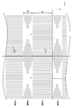
図2及び図3を参照して、スケール20におけるスケール格子21の構成について説明する。図2及び図3は、スケール20(スケール格子21)の一部を拡大して示す平面図である。スケール格子21は、位置検出方向、即ち、移動方向(X方向)に垂直な方向(Y方向)において、2種類の領域A及びBを交互に配列して構成されている。
The configuration of the scale grating 21 in the
領域Aは、X方向に沿って、ピッチP1(=8μm)ごとに、P1/2の幅の反射膜が形成された格子パターン列(相対移動方向に第1空間周波数を有する第1格子パターン)を有する。領域Bは、X方向に沿って、ピッチP2(=512μm)ごとに、図3に示すパターン22が配列されたパターン列(相対移動方向に第1空間周波数より低い第2空間周波数を有する第2格子パターン)を有する。また、領域Bのパターンのピッチは、領域Aのパターンのピッチの4倍以上、好ましくは、8倍以上であるとよい。領域AのY方向における幅W1は50μmであり、領域BのY方向における幅W2は25μmである。
Region A is a grid pattern row (first grid pattern having a first spatial frequency in the direction of relative movement) formed with a reflective film having a width of P1/2 at every pitch P1 (=8 μm) along the X direction. have Region B has a pattern row (a second spatial frequency having a second spatial frequency lower than the first spatial frequency in the direction of relative movement) in which the
図3に示す領域Bのパターン22について説明する。Y方向の中心からの距離がW2×1/8以下の領域において、反射膜23のX方向の幅は、P2×185/240である。Y方向の中心からの距離がW2×1/8からW2×1/4までの領域において、反射膜23のX方向の幅は、P2×141/240である。Y方向の中心からの距離がW2×1/4からW2×3/8までの領域において、反射膜23のX方向の幅は、P2×105/240である。Y方向の中心からの距離がW2×3/8からW2×1/2までの領域において、反射膜23のX方向の幅は、P2×61/240である。このように、スケール格子21の移動方向に垂直な方向において、反射膜23の幅を異ならせることで、センサユニット10とスケール20との距離に対し、広い範囲で高周波成分をキャンセルすることができる。
The
図4及び図5は、本実施形態における受光素子アレイ12を構成する複数の受光素子121の配列を示す図である。本実施形態では、受光素子アレイ12は、32個の受光素子121が位置検出方向に一列に並べられて構成されている。位置検出方向において互いに隣り合う2つの受光素子121の中心間距離(隣接素子ピッチ)Xpdは、64μmである。また、各受光素子121の位置検出方向に直交する方向のサイズ(幅)Ypdは、450μmである。
4 and 5 are diagrams showing the arrangement of the plurality of light receiving
各受光素子121からの出力は、スイッチ回路18を介して切り替えられ、選択的に後段の4つの初段増幅器(不図示)に接続されている。4つの初段増幅器のそれぞれには、出力端子A+、B+、A-、B-(それぞれ、A+相、B+相、A-相、B+相を表す)に対応する受光素子121が接続される。4つの初段増幅器は、スケール20の移動に応じて、その値が正弦波状に変化する4相正弦波出力S(A+)、S(B+)、S(A-)、S(B-)を出力する。
The output from each light receiving
スイッチ回路18は、信号処理部30の信号分離部31からの入力に応じて、受光素子121と初段増幅器の出力端子との接続を切り替える。これにより、複数の受光素子121において、電気的に加算される間隔が切り替わる。換言すれば、スイッチ回路18は、複数の受光素子121において出力を加算すべき、相対移動方向に連続した受光素子121の数を設定する処理を行う処理部として機能する。
The
信号処理部30からの入力がハイレベルである場合には、図4に示すように、電気的に接続されている受光素子121の中心間距離Ppdは、256μmとなる。また、信号処理部30からの入力がローレベルである場合には、図5に示すように、電気的に接続されている受光素子121の中心間距離Ppdは、1024μmとなる。
When the input from the
4相正弦波状信号の相対位相は、それぞれの検出ピッチに対し、S(A+)を基準とすると、S(B+)は約+90度、S(A-)は約+180度、S(B-)は約+270度の関係にある。 The relative phases of the four-phase sinusoidal signals are, with respect to each detection pitch, when S(A+) is used as a reference, S(B+) is approximately +90 degrees, S(A-) is approximately +180 degrees, and S(B-) is have a relationship of about +270 degrees.
信号処理部30は、4相正弦波出力S(A+)、S(B+)、S(A-)、S(B-)に対して、以下の式(1)及び式(2)に示す演算を行うことで、直流分が除去された2相正弦波状信号S(A)及びS(B)を生成する。
The


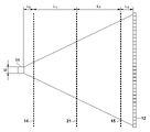
図6は、本実施形態におけるエンコーダ1の光路の展開図、即ち、反射を透過として示す図である。発光素子11から光源格子14までの距離L0は、0.3mmに設定されている。スケール格子21からインデックス格子15までの距離L2は、光源格子14からスケール格子21までの距離L1と等しく、或いは、等しいとみなせる範囲内に設定され、本実施形態では、L1=L2=1mmに設定されている。インデックス格子15から受光素子アレイ12までの距離L3は、0.3mmに設定されている。ここで、それぞれの距離L0、L1、L2、L3は、幾何光学上の実効光路長として、物理長を屈折率で除した値として示されている。また、発光素子11の位置検出方向における発光領域幅Wは32μmであり、発光素子11からの光の波長(発光波長)λは650nmである。
FIG. 6 is a developed view of the optical path of the
図7は、スケール側から見たセンサユニット10を示す図である。光源格子14の格子ピッチは、8μmである。本実施形態において、インデックス格子15は、位置検出方向における格子ピッチが位置検出方向に直交する方向に連続して変化している。L0=L1=1mmにおいて、発光素子11から受光素子アレイ12に入射する光の主光線(中心光線)とインデックス格子15と交わる位置をY=0とし、発光素子11に近づく方向を正(Y>0)とする。インデックス格子15の位置検出方向の格子ピッチP3(Y)は、以下の式(3)で表される関数に従う。
FIG. 7 is a diagram showing the

ここで、インデックス格子15の周期を位置検出方向に直交する方向で変化させているのは、特開2015-200568号公報に開示されているように、L0、L1の変化による2相正弦波状信号S(A)、S(B)の信号振幅や位相差を安定させるためである。但し、本発明は、これに限定されるものではなく、インデックス格子15の周期を位置検出方向に直交する方向で一様としてもよい。 Here, the period of the index grating 15 is changed in the direction orthogonal to the position detection direction because, as disclosed in Japanese Unexamined Patent Application Publication No. 2015-200568 , two-phase sinusoidal This is for stabilizing the signal amplitude and phase difference of the wave signals S(A) and S(B). However, the present invention is not limited to this, and the period of the index grating 15 may be uniform in the direction orthogonal to the position detection direction.
高分解能モードの光学作用について説明する。高分解能モードでは、スケール格子21の領域Aのパターン(格子パターン列)に対応する信号(周期信号)を取得する。高分解能モードでは、3格子構成において、第1格子を光源格子14、第2格子をスケール格子21、第3格子をインデックス格子15として作用させて検出を行う。高分解能モードでは、スケール格子21とインデックス格子15とでモアレを発生させる。 The optical action of the high resolution mode will be explained. In the high resolution mode, a signal (periodic signal) corresponding to the pattern (grid pattern row) of the area A of the scale grating 21 is obtained. In the high-resolution mode, the first grating acts as the light source grating 14, the second grating as the scale grating 21, and the third grating as the index grating 15 in a three-grating configuration for detection. In the high resolution mode, the scale grating 21 and the index grating 15 generate moire.
発光素子11から射出した光(発散光束)は、光源格子14を通過することで、互いにインコヒーレントなピッチごとに配置された複数の光源アレイを形成する。光源格子14から射出した光は、スケール格子21に入射する。なお、発光素子11が半導体レーザやスーパールミネッセントダイオード(SLD)などの微小発光点を有する光源であれば、光源格子14を省略することも可能である。
Light (divergence light flux) emitted from the
スケール格子21の領域Aのパターンによって回折及び反射した+1次回折光及び-1次回折光は、インデックス格子15で互いに干渉する。これにより、8μm周期の強度分布を有する干渉縞Aがインデックス格子15の上に形成される。干渉縞Aの空間周波数fimageは、領域Aのパターン周波数fAを用いて、以下の式(4)で表される。 The +1st-order diffracted light and -1st-order diffracted light diffracted and reflected by the pattern of the area A of the scale grating 21 interfere with each other at the index grating 15 . As a result, interference fringes A having an intensity distribution of 8 μm period are formed on the index grating 15 . The spatial frequency f image of the interference fringes A is expressed by the following equation (4) using the pattern frequency f A of the area A.

式(4)において、kは干渉縞の次数(干渉次数に対応する自然数)であり、±1次回折光同士の干渉縞を用いる場合は、k=2とする。なお、0次光と±1次回折光との干渉縞を用いる場合は、k=1となる。 In Equation (4), k is the order of the interference fringes (a natural number corresponding to the order of interference), and k=2 when interference fringes of ±1st-order diffracted lights are used. Note that k=1 when the interference fringes of the 0th-order light and the ±1st-order diffracted lights are used.
一方、インデックス格子15の格子周波数findex(=1/P3(Y))は、空間周波数fimageと僅かにずれているため、もとの干渉縞に対して粗い空間周波数fmがうなりとして重畳された強度分布がインデックス格子15を通過する。このように、インデックス格子15は、領域Aのパターンからの干渉像の空間周波数から予め定められた周波数オフセット量だけオフセットさせた空間周波数(第3空間周波数)を有する。インデックス格子15の格子周波数をfindexとすると、干渉縞とのうなり空間周波数fmは、以下の式(5)で表される。 On the other hand, since the grating frequency f index (=1/P3(Y)) of the index grating 15 is slightly deviated from the spatial frequency f image , the coarse spatial frequency f m is superimposed on the original interference fringes as a beat. The resulting intensity distribution passes through index grating 15 . Thus, the index grating 15 has a spatial frequency (third spatial frequency) that is offset from the spatial frequency of the interference image from the region A pattern by a predetermined frequency offset amount. Assuming that the grating frequency of the index grating 15 is f index , the beat spatial frequency f m with the interference fringes is expressed by the following equation (5).

インデックス格子15を通過した空間周波数fmの強度分布は、更に伝搬して、像倍率M1で受光素子アレイ12に投影される。像倍率M1は、以下の式(6)で表される。但し、実効的な距離L0は、光源格子14の有効サイズなどにも影響され、実際の距離L0よりも小さく作用することもある。
The intensity distribution of the spatial frequency fm that has passed through the index grating 15 propagates further and is projected onto the light receiving

領域Aのパターンによって受光素子アレイ12に形成される強度分布の空間周波数fimageAは、以下の式(7)で表される。
The spatial frequency f imageA of the intensity distribution formed on the light receiving

本実施形態では、k=2、M1=1.13である。空間周波数fimageAは、受光素子アレイ12で受光する範囲において、以下の式(8)で示す強度分布を有する。
In this embodiment, k=2 and M 1 =1.13. Spatial frequency f imageA has an intensity distribution represented by the following equation (8) in the range of light received by the light receiving

低分解能モードの光学作用について説明する。低分解能モードでは、スケール格子21の領域Bのパターンに対応する信号(周期信号)を取得する。低分解能モードでは、3格子構成において、第1格子を発光素子11、第2格子をスケール格子21、第3格子を受光素子アレイ12として作用させて検出を行う。低分解能モードでは、インデックス格子15を機能させず、モアレを発生させない。
The optical action of the low resolution mode will be explained. In the low resolution mode, a signal (periodic signal) corresponding to the pattern of area B of scale grating 21 is obtained. In the low resolution mode, detection is performed by using the first grating as the
発光素子11から射出した光(発散光束)は、光源格子14を経て、スケール格子21に入射する。スケール格子21の領域Bのパターンによって回折及び反射した0次回折光と±1次回折光は、インデックス格子15を経て、受光素子アレイ12の上で互いに干渉し、像倍率M2で干渉縞Bが形成される。像倍率M2は、以下の式(9)で表される。
Light (divergence luminous flux) emitted from the

スケール20が反射型スケールである場合、本実施形態のように、発光素子11と受光素子アレイ12とをほぼ同一面上に形成することで、センサユニット10とスケール20との距離にかかわらず、M2=2でほぼ一定とすることができる。
When the
なお、発光素子11から射出した光は、往路で光源格子14、復路でインデックス格子15を通過するが、対応する(格子周期のオーダーが近い)格子構造がスケール格子の領域Bに存在しないため、形成される干渉縞には強く関与しない。但し、後述するように、インデックス格子15の回折によるコントラストの低下には配慮する必要がある。
The light emitted from the
干渉縞Bの空間周波数fimageBは、領域Bのパターンの格子周波数fB(=1/P2)を用いて、以下の式(10)で表される。 The spatial frequency f imageB of the interference fringes B is represented by the following equation (10) using the grating frequency f B (=1/P2) of the pattern of the area B.

本実施形態では、k=1、M2=2である。空間周波数fimageBは、以下の式(11)で示す強度分布を有する。 In this embodiment, k=1 and M 2 =2. Spatial frequency f imageB has an intensity distribution given by the following equation (11).

次に、それぞれの分解能モードでの受光素子121の配列設定によって、互いの周期信号を分離する作用について説明する。図8は、高分解能モードと低分解能モードでの受光素子アレイ12の空間周波数応答を示す図である。実線が高分解能モードでの空間周波数応答であり、破線が低分解能モードでの空間周波数応答である。
Next, the effect of separating periodic signals from each other by setting the arrangement of the
高分解能モードでは、スイッチ回路18がハイに設定され、受光素子アレイ12の電気的に接続されている受光素子121の中心間距離Ppdは256μmに設定される。受光素子アレイ12(受光素子121)の空間周波数応答のピークは、1/256[μm-1]付近である。受光素子アレイ12に形成される強度分布の空間周波数fimageAの範囲が空間周波数応答のピーク付近にあるため、スケール格子21の領域Aのパターンの成分を効率よく検出することができる。一方、スケール格子21の領域Bのパターンからの干渉像の空間周波数fimageB(=1/1024[μm-1])付近に対しては、空間周波数応答が相対的に低くなっており、外乱としての信号変動が抑えられていることがわかる。高分解能モードでは、受光素子アレイ12の空間周波数応答のピークを、インデックス格子15の周波数オフセット量に対応する空間周波数より低い空間周波数(第4空間周波数)に近づけるように、出力を加算すべき受光素子121の数(第1数)を設定する。
In the high resolution mode, the
低分解能モードでは、スイッチ回路18がローに設定され、受光素子アレイ12の電気的に接続されている受光素子121の中心間距離Ppdは1024μmに設定される。受光素子アレイ12(受光素子121)の空間周波数応答のピークは、1/1024[μm-1]付近である。受光素子アレイ12に形成される強度分布の空間周波数fimageB(=1/1024[μm-1])と、空間周波数応答のピークとがほぼ一致しているため、スケール格子21の領域Bのパターンの成分を効率よく検出することができる。一方、スケール格子21の領域Aのパターンからの強度分布に対応する空間周波数fimageAの範囲に対しては、空間周波数応答が相対的に低くなっており、外乱としての信号変動が抑えられていることがわかる。低分解能モードでは、受光素子アレイ12の空間周波数応答のピークを、領域Bのパターンからの干渉像の空間周波数に近づけるように、出力を加算すべき受光素子121の数(第1数とは異なる第2数)を設定する。
In the low resolution mode, the
高分解能モードにおける受光素子アレイ12の空間周波数応答のピーク周波数fpeak1と、低分解能モードにおける受光素子アレイ12の空間周波数応答のピーク周波数fpeak2との関係は、fpeak1>fpeak2となっている。より好ましくは、1.2<fpeak1÷fpeak2<4.0(更に好ましくは3.0)であるとよい。また、低分解能モードにおける受光素子アレイ12の空間周波数応答のピーク周波数fpeakは、スケール格子21の領域BのパターンのピッチをP2、干渉次数に対応する自然数をkとして、以下の式で表される。
The relationship between the peak frequency f peak1 of the spatial frequency response of the light

図9は、高分解能モード及び低分解能モードのそれぞれで得られる信号波形を示す図である。高分解能モードでの信号周期SpAは、P1/k=4μmである。低分解能モードでの信号周期SpBは、P2/k=512μmである。 FIG. 9 is a diagram showing signal waveforms obtained in each of the high resolution mode and the low resolution mode. The signal period SpA in high resolution mode is P1/k=4 μm. The signal period SpB in the low resolution mode is P2/k=512 μm.
高分解能モードと低分解能モードでの信号周期の切り替え比率は、4μmと512μmであるため、128倍である。一方、各モードで切り替えられる、連続して足し合わされる受光素子の数の比率は、1個と4個の4倍であり、信号周期の比率に対して非常に小さく抑えられている。これにより、各受光素子間の分離帯の増加による受光効率の低下、及び、接合容量の増大を防止することができる。 The signal cycle switching ratio between the high resolution mode and the low resolution mode is 128 times because it is 4 μm and 512 μm. On the other hand, the ratio of the number of light-receiving elements that are continuously added and switched in each mode is 4 times, ie, 1 and 4, and is suppressed to a very small value with respect to the ratio of the signal period. As a result, it is possible to prevent a decrease in light receiving efficiency and an increase in junction capacitance due to an increase in the separation band between the light receiving elements.
このように、本実施形態におけるエンコーダ1は、高分解能モードと低分解能モードとの切り替えにおいて、3格子構成における各光学素子の作用を異ならせている。これにより、高い分解能切り替え比率を有しながら、高い応答性及び検出効率を実現することができる。
In this way, the
なお、エンコーダ1においては、スケール格子21の領域Bからの干渉縞のインデックス格子15(光学格子上)での周期、及び、インデックス格子15の周期のうち、長い方の周期が短い方の周期の3倍未満、好ましくは、1.5倍未満であるとよい。
In the
次に、高分解能の絶対位置情報を取得するための処理について説明する。第1位相取得部32は、スイッチ回路18への入力がハイレベルである場合の2相正弦波状信号S(A)、S(B)に基づいて、スケール格子21の領域Aのエネルギー分布の位相(位相信号)Φ1を、以下に示す式(12)の演算によって取得する。なお、ATAN2[Y,X]は、象限を判別して0~2πの位相に変換する逆正接演算関数である。
Next, processing for acquiring high-resolution absolute position information will be described. The first

同様に、第2位相取得部33は、スイッチ回路18への入力がローレベルである場合の2相正弦波状信号S(A)、S(B)に基づいて、スケール格子21の領域Bのエネルギー分布の位相(位相信号)Φ2を、以下に示す式(13)の演算によって取得する。
Similarly, the second

本実施形態の位置情報取得部34は、第1位相取得部32の出力を相対位置信号として取得する。相対位置信号の変化を計数することによって、スケール20が検出開始位置から所定周期として何周期目に位置するかの情報を取得することができる。
The position
スイッチ回路18への入力の切り替え前後で、時間差をおかずに信号を取得することで、ほぼ同一位置での位相Φ1及びΦ2を得ることができる。
By obtaining signals without a time difference before and after switching the input to the
本実施形態では、図4及び図5に示すように、受光素子アレイ12の複数の受光素子121の少なくとも一部は、位相Φ1を取得するための受光素子121及び位相Φ2を取得するための受光素子121として共通して用いられる。これにより、従来技術のように、位相Φ1を取得するための受光素子と位相Φ2を取得するための受光素子とを別々に設ける場合と比べて、受光素子アレイ12を小型化することができる。
In this embodiment, as shown in FIGS. 4 and 5, at least some of the plurality of light receiving
信号処理部30は、以下の式(14)に示す演算によって、位相Φ2の周期内で位相Φ1の周期の何番目にあるかを求め、位相Φ1をつなぎ合わせて位相Φ1の位置精度を有する絶対位置信号ABSを取得する。このような処理を行うことで、高精度なインクリメントパターン信号の精度で、長ストロークの絶対位置を検出することができる。
The

発光素子11(光源)のサイズの影響について説明する。図10は、受光素子アレイ12に形成される強度分布の空間周期を256μmとした場合における発光素子11のサイズ(発光サイズ)Wに対する信号振幅の減衰の様子を示す図である。
The influence of the size of the light emitting element 11 (light source) will be described. FIG. 10 is a diagram showing attenuation of signal amplitude with respect to the size (emission size) W of the
高分解能モードにおけるスケール格子21の領域Aのパターンによる干渉像の受光素子アレイ上での光量分布は、発光サイズWに対し、以下の式(15)に示す光学横倍率MLED1を適用した上で、点光源像に畳み込みを行った分布で近似が可能である。高分解能モードでは、受光素子アレイ上の空間周期と発光サイズWとが近づいても、受光素子アレイ上でのコントラストは殆ど変化しない。 The light amount distribution on the light receiving element array of the interference image of the pattern of the area A of the scale grating 21 in the high resolution mode is obtained by applying the optical lateral magnification M LED1 shown in the following equation (15) to the light emission size W: , can be approximated by a distribution obtained by convolving the point light source image. In the high resolution mode, the contrast on the light receiving element array hardly changes even if the spatial period on the light receiving element array and the light emission size W are close to each other.

一方、低分解能モードにおけるスケール格子21の領域Bのパターンによる干渉像の受光素子アレイ上での光量分布も近似が可能である。具体的には、発光サイズWに対し、以下の式(16)に示す光学横倍率MLED2を適用した上で、微小点光源による干渉像に畳み込みを行った分布で近似が可能である。 On the other hand, it is also possible to approximate the light amount distribution on the light receiving element array of the interference image by the pattern of the area B of the scale grating 21 in the low resolution mode. Specifically, after applying the optical lateral magnification M LED2 shown in the following equation (16) to the light emission size W, it is possible to approximate the distribution by convolving the interference image due to the minute point light source.

本実施形態では、光学横倍率MLED2が1であるため、低分解能モードでは、受光素子アレイ上の空間周期と発光サイズWとが近づくと、受光素子アレイ上でのコントラストは消失する。 In this embodiment, the optical lateral magnification M LED2 is 1, so in the low resolution mode, when the spatial period on the light receiving element array and the light emission size W become closer, the contrast on the light receiving element array disappears.
式(15)及び式(16)を参照するに、MLED2>MLED1が明らかであるため、受光素子アレイ上の強度分布の空間周期を同一に設定した場合、高分解能モードは、低分解能モードと比べて、発光サイズWの影響による減衰が小さい。換言すれば、本実施形態のように、検出対象の受光素子アレイ上の強度分布に対応する受光素子の配列周期を、低分解能モードと比べて、高分解能モードで小さくすることが、信号効率の観点から好ましい。 Referring to equations (15) and (16), it is clear that M LED2 >M LED1 . Therefore, when the spatial period of the intensity distribution on the light receiving element array is set to be the same, the high resolution mode is the low resolution mode Attenuation due to the influence of the emission size W is small compared to . In other words, as in the present embodiment, reducing the array period of the light-receiving elements corresponding to the intensity distribution on the light-receiving element array to be detected in the high-resolution mode compared to the low-resolution mode increases the signal efficiency. preferable from this point of view.
次いで、インデックス格子15による回折の影響について説明する。受光素子アレイ上の強度分布が良好なコントラストを得るためには、インデックス格子15の回折による縞の消失を避けなければならない。インデックス格子15から受光素子アレイ12への伝搬に伴う光線シフト量が、受光素子アレイ上の強度分布の周期の半分に達すると、コントラストが極小となる。
Next, the influence of diffraction by the index grating 15 will be explained. In order to obtain good contrast in the intensity distribution on the light receiving element array, it is necessary to avoid disappearance of fringes due to diffraction of the index grating 15 . The contrast becomes minimal when the light beam shift amount due to propagation from the index grating 15 to the light receiving
受光素子アレイ上の強度分布の周期は、高分解能モードにおいて、1/fimageAであり、低分解能モードにおいて、1/fimageBである。一方、空間周波数findexのインデックス格子15による回折角θは、発光素子11からの光の波長をλとして、sinθ=findex・λである。インデックス格子15から受光素子アレイ12への伝搬に伴う光線シフト量は、L3・tanθで表される。ここで、sinθ≒tanθ≒θと近似すると、良好なコントラストが得られる条件は、高分解能モードでは、以下の式(17)となり、低分解能モードでは、以下の式(18)となる。なお、Δfは、インデックス格子15の周波数オフセット量である。
The period of the intensity distribution on the photodetector array is 1/f imageA in the high resolution mode and 1/f imageB in the low resolution mode. On the other hand, the diffraction angle θ of the spatial frequency f index by the index grating 15 is sin θ=f index ·λ, where λ is the wavelength of the light from the


<第2実施形態>
本実施形態において、スケール20は、石英基板に加工された段差部がスケール格子21(領域A及びB)としてパターニングされている。かかる段差部は、エッチングによって、発光素子11からの光の波長の1/4程度の深さで形成され、表面には、反射膜としてのアルミ膜及び誘電体膜が積層されている。
<Second embodiment>
In this embodiment, the
図11を参照して、スケール20におけるスケール格子21の構成について説明する。図11は、スケール格子21の一部を拡大して示す平面図であって、グレー部分が段差部の凹部である。スケール格子21は、相対移動方向に垂直な方向において、2種類の領域A及びBを交互に配列して構成されている。
The configuration of scale grating 21 in
領域Aは、X方向に沿って、ピッチP1(=8μm)ごとに、P1/2の幅の凹部が形成された格子パターン列を有する。領域Bは、X方向に沿って、ピッチP2(=512μm)ごとに、P2/2の幅の凹部が形成されたサブ格子領域24を有する。また、各サブ格子領域24において、X方向に沿って、ピッチPsubごとに、Psub/2の幅の凹部が形成された微細なサブ格子を含む構造を有する。本実施形態において、ピッチPsub(サブ格子周期)は、1.65μmである。領域AのY方向における幅W1は50μmであり、領域BのY方向における幅W2は25μmである。
The region A has a lattice pattern row in which recesses having a width of P1/2 are formed at pitches P1 (=8 μm) along the X direction. Region B has
スケール格子21の格子周期が概ね10μm以下の格子周期であれば、発光素子11からの光の波長幅による平均化効果、及び、受光素子アレイ12での光路長の違いによる平均化効果によって、ギャップ依存性が小さい安定したコントラストを得ることができる。但し、スケール格子21の格子周期が10μm以上である場合、高次回折光の干渉によって、良好なコントラストが得られる伝搬長の範囲が制限される。かかる伝搬長Lは、低分解能モードでは、以下の式(19)で表され、高分解能モードでは、以下の式(20)で表される。
If the grating period of the scale grating 21 is about 10 μm or less, the averaging effect due to the wavelength width of the light from the


格子構造が同じ場合、波長λと信号周期Spとの関係、Sp2/λで正規化される伝搬長Lに応じて、コントラストが周期的に変化する。従って、共通の伝搬長において、周期信号Spが著しく異なる複数の領域において同時に良好なコントラストを得ることができない場合がある。特に、位相格子構造において、L<0.5・Sp2/λの領域、即ち、短い伝搬長において、大きい格子周期の干渉像のコントラストが得られない。 For the same grating structure, the contrast changes periodically depending on the relationship between the wavelength λ and the signal period Sp, the propagation length L normalized by Sp2/λ. Therefore, it may not be possible to simultaneously obtain good contrast in a plurality of regions in which the periodic signals Sp are significantly different in the common propagation length. In particular, in the phase grating structure, in the region of L<0.5·Sp 2 /λ, that is, in the short propagation length, the contrast of the interference image with a large grating period cannot be obtained.
そこで、本実施形態では、各サブ格子領域24が微細なサブ構造を有する構造とすることで、上述した問題を改善している。サブ格子領域24のピッチPsubは、設計中心の伝搬長をLcとして、以下の式(21)の付近とするとよい。
Therefore, in the present embodiment, each

また、式(21)は、サブ格子領域24の空間周波数(第5空間周波数)fsubとして、以下の式でも表される。但し、発光素子11とスケール格子21との間の距離をLa(=L0+L1)とし、スケール格子21と受光素子アレイ12との間の距離をLb(=L2+L3)とする。
Equation (21) is also expressed by the following equation as the spatial frequency (fifth spatial frequency) f sub of the

サブ格子領域24のサブ格子が1本である場合には、そのサブ格子の幅をPsub/2とする。図12は、サブ格子領域24のサブ格子を1本、3本、5本とした場合における伝搬長Lに対する干渉像のコントラスト(P2周期変調振幅/DC成分)を示すグラフである。図12を参照するに、サブ格子を増やすにつれて、コントラストのピークが近接側にシフトしていくことがわかる。これにより、L<0.5・Sp2/λの条件下において、有効な干渉像のコントラストを向上することができる。
If the
このように、本実施形態におけるエンコーダ1は、高分解能モードと低分解能モードとの切り替え比率を大きくした場合において、検出効率を向上させることができる。
As described above, the
<第3実施形態>
図13及び図14は、本実施形態における受光素子アレイ12を構成する複数の受光素子121の配列を示す図である。本実施形態では、受光素子アレイ12は、64個の受光素子121が位置検出方向に一列に並べられて構成されている。位置検出方向において互いに隣り合う2つの受光素子121の中心間距離Xpdは、32μmである。また、各受光素子121の位置検出方向に直交する方向のサイズ(幅)Ypdは、450μmである。
<Third Embodiment>
13 and 14 are diagrams showing the arrangement of the plurality of light receiving
スイッチ回路18は、信号処理部30の信号分離部31からの入力に応じて、受光素子121と初段増幅器の出力端子との接続を切り替える。これにより、複数の受光素子121において、電気的に加算される間隔が切り替わる。
The
信号処理部30からの入力がハイレベルである場合、図13に示すように、64個の受光素子121のうち左右にそれぞれ16個ずつある受光素子121は、信号を取り出す受光素子121が連続する2個のうちの1個となっている。従って、中央の32個の受光素子121からの出力信号に対して両側のそれぞれの16個の受光素子121からの出力信号の重み付けは1/2になる。
When the input from the
信号処理部30からの入力がローレベルである場合、図14に示すように、64個の受光素子121のうち左右にそれぞれ16個ずつある受光素子121は、信号を取り出す受光素子121が連続する8個のうちの4個とし、且つ、中央の2個を用いていない。このように、本実施形態では、センサユニット10に重み付けが設けられている。これにより、互いの信号分離精度を向上させることができる。
When the input from the
図15は、高分解能モードと低分解能モードでの受光素子アレイ12の空間周波数応答を示す図である。実線が高分解能モードでの空間周波数応答であり、破線が低分解能モードでの空間周波数応答である。図8と比較して、空間周波数fimageB付近においては、高分解能モードでの空間周波数応答が低減され、空間周波数fimageAの範囲においては、低分解能モードでの空間周波数応答が低減されている。
FIG. 15 is a diagram showing spatial frequency responses of the light
このように、本実施形態におけるセンサユニット10では、高分解能モードと低分解能モードとの切り替えにおける信号の分離精度を向上させることができる。
Thus, in the
<第4実施形態>
図16は、第1実施形態で説明したエンコーダ1を有する装置の一例としての露光装置500の構成を示す概略図である。露光装置500は、半導体デバイスや液晶表示素子の製造工程であるリソグラフィ工程に用いられ、基板(半導体ウエハ)にパターン(電子回路パターン)を形成するリソグラフィ装置である。露光装置500では、エンコーダ1を、基板を保持して2次元方向に移動するステージの位置を検出するために用いている。
<Fourth Embodiment>
FIG. 16 is a schematic diagram showing the configuration of an
ステージ50は、動作可能な可動部であって、基板53を保持する。投影光学系51は、基板53に対して、マスク(不図示)のパターンの光学像(パターン像)を投影(露光)する光学系である。駆動部55は、ステージ50を、投影光学系51に対してX方向及びY方向に駆動する。これにより、基板上におけるマスクのパターン像の投影位置が制御される。
The
本実施形態では、エンコーダ1のスケール20は、ステージ50に取り付けられ、エンコーダ1のセンサユニット10は、露光装置500の固定部である筐体54に取り付けられている。なお、エンコーダ1として、実施形態2や実施形態3で説明したものを用いてもよい。
In this embodiment, the
制御部56は、センサユニット10の受光素子アレイ12からの出力からステージ50の位置を求め、求めたステージ50の位置に基づいて駆動部55を制御する。換言すれば、制御部56は、エンコーダ1の検出結果に基づいて、ステージ50の位置を制御する。
The
このように、本実施形態では、露光装置500のステージ50の位置を、第1実施形態で説明したエンコーダ1を用いて、高分解能に、且つ、安定的に検出することで、ステージ50の移動(動作)を高精度に制御することができる。なお、第1実施形態、第2実施形態及び第3実施形態で説明したエンコーダ1は、露光装置に限らず、ロボットアームや搬送装置などの様々な装置における可動部の位置の検出に用いることができる。
As described above, in the present embodiment, the position of the
本発明の実施形態における物品の製造方法は、例えば、デバイス(半導体素子、磁気記憶媒体、液晶表示素子など)などの物品を製造するのに好適である。かかる製造方法は、露光装置500を用いて、感光剤が塗布された基板を露光する(パターンを基板に形成する)工程と、露光された基板を現像する(基板を処理する)工程を含む。また、かかる製造方法は、他の周知の工程(酸化、成膜、蒸着、ドーピング、平坦化、エッチング、レジスト剥離、ダイシング、ボンディング、パッケージングなど)を含みうる。本実施形態における物品の製造方法は、従来に比べて、物品の性能、品質、生産性及び生産コストの少なくとも1つにおいて有利である。
The method for manufacturing an article according to the embodiment of the present invention is suitable for manufacturing articles such as devices (semiconductor elements, magnetic storage media, liquid crystal display elements, etc.). This manufacturing method includes a step of exposing a substrate coated with a photosensitive agent (forming a pattern on the substrate) and a step of developing the exposed substrate (processing the substrate) using the
<第5実施形態>
本実施形態では、第1実施形態で説明したエンコーダ1を、外力を検出する力覚センサに応用した例を説明する。図17は、本実施形態における光学式の力覚センサ600の構成を示す概略図である。力覚センサ600は、力センサ部610と、処理部620と、を有する。力センサ部610は、外力によって力センサ部内の変位部612に生じた変位を示す変位信号を処理部620に出力する。処理部620は、力センサ部610から入力された変位信号に基づいて外力のベクトル量を求め、その結果を力覚信号として出力する。
<Fifth Embodiment>
In this embodiment, an example in which the
力センサ部610は、ベース部611と、変位部612と、ベース部611と変位部612とを連結して支持する弾性支持部(弾性部材)613と、変位検出部614と、を含む。変位検出部614は、センサユニット10やスケール20で構成されるエンコーダ1を含み、ベース部611に対する変位部612の変位(変位部612の位置)を検出する。変位検出方向は、図17において、X方向である。変位部612は、変位部612に作用する外力に応じて、弾性支持部613を弾性変形させながらベース部611に対してZ軸周りでの回転変位が可能である。外力は、センサユニット10とスケール20との相対変位量とほぼ比例関係にある。従って、エンコーダ1の位置検出値に係数をかけることで、外力に変換することができる(即ち、変位部612に作用する外力を検出することができる)。
The
また、本実施形態の力覚センサ600を有する様々な装置も本発明の一側面を構成する。かかる装置は、例えば、可動部と、力覚センサ600と、力覚センサ600を用いて可動部の動作を制御する制御部と、を有する。
Various devices having the
以上、本発明の好ましい実施形態について説明したが、本発明はこれらの実施形態に限定されないことはいうまでもなく、その要旨の範囲内で種々の変形及び変更が可能である。 Although the preferred embodiments of the present invention have been described above, it goes without saying that the present invention is not limited to these embodiments, and various modifications and changes are possible within the scope of the gist.
1:エンコーダ 10:センサユニット 12:受光素子アレイ 14:光源格子 15:インデックス格子 20:スケール 21:スケール格子 30:信号処理部 1: Encoder 10: Sensor Unit 12: Photodetector Array 14: Light Source Grating 15: Index Grating 20: Scale 21: Scale Grating 30: Signal Processing Section
Claims (13)
前記スケールは、前記スケールと前記検出器との相対移動方向に第1空間周波数を有する第1格子パターンと、前記相対移動方向に前記第1空間周波数より低い第2空間周波数を有する第2格子パターンと、を含み、前記第2格子パターンのピッチは、前記第1格子パターンのピッチの8倍以上であり、
前記検出器は、前記相対移動方向に沿って配置された複数の受光素子を含み、
前記位置検出装置は、
前記スケールと前記検出器との間に設けられ、前記相対移動方向に前記第1格子パターンからの干渉像の空間周波数から予め定められた周波数オフセット量だけオフセットさせた第3空間周波数を有する光学格子と、
第1分解能モードでは、前記第1格子パターン及び前記光学格子を通過した光から前記周波数オフセット量に対応する空間周波数より低い第4空間周波数の成分の位相が検出されるように、前記第1分解能モードよりも分解能が低い第2分解能モードでは、前記第2格子パターン及び前記光学格子を通過した光から前記第2格子パターンの干渉像の空間周波数の成分の位相が検出されるように、前記複数の受光素子において出力を加算すべき、前記相対移動方向に連続した受光素子の数を設定する処理を行う処理部と、
を有することを特徴とする位置検出装置。 A position detection device that includes a scale and a detector, one of which is provided on an object, and detects the position of the object by detecting light from the scale with the detector,
The scale has a first grating pattern having a first spatial frequency in the direction of relative movement between the scale and the detector, and a second grating pattern having a second spatial frequency lower than the first spatial frequency in the direction of relative movement. and, wherein the pitch of the second lattice pattern is eight times or more the pitch of the first lattice pattern,
The detector includes a plurality of light receiving elements arranged along the direction of relative movement,
The position detection device is
An optical grating provided between the scale and the detector and having a third spatial frequency offset in the relative movement direction from the spatial frequency of the interference image from the first grating pattern by a predetermined frequency offset amount. When,
In the first resolution mode, the phase of the component of the fourth spatial frequency lower than the spatial frequency corresponding to the frequency offset amount is detected from the light that has passed through the first grating pattern and the optical grating. In the second resolution mode, which has a lower resolution than the mode, the plurality of a processing unit that performs processing for setting the number of continuous light receiving elements in the direction of relative movement to which the outputs of the light receiving elements are to be added;
A position detection device comprising:
fpeak1>fpeak2
を満たすことを特徴とする請求項1乃至3のうちいずれか1項に記載の位置検出装置。 The relationship between the peak frequency f peak1 of the spatial frequency response of the detector in the first resolution mode and the peak frequency f peak2 of the spatial frequency response of the detector in the second resolution mode is
f peak1 >f peak2
4. The position detecting device according to any one of claims 1 to 3 , wherein:

前記位相格子は、前記第2空間周波数より高い第5空間周波数を有するサブ格子を含むことを特徴とする請求項1乃至6のうちいずれか1項に記載の位置検出装置。 the second grating pattern includes a phase grating in which regions having different optical path lengths are periodically formed in the direction of relative movement;
7. A position detecting device according to any one of claims 1 to 6 , wherein the phase grating includes sub-gratings having a fifth spatial frequency higher than the second spatial frequency.


前記基板を保持して移動するステージと、
前記ステージの位置を対象物の位置として検出する請求項1乃至10のうちいずれか1項に記載の位置検出装置と、
前記位置検出装置の検出結果に基づいて、前記ステージの位置を制御する制御部と、
を有することを特徴とするリソグラフィ装置。 A lithographic apparatus for patterning a substrate, comprising:
a stage that holds and moves the substrate;
a position detection device according to any one of claims 1 to 10 , which detects the position of the stage as the position of the object;
a control unit that controls the position of the stage based on the detection result of the position detection device;
A lithographic apparatus comprising:
前記ベース部に対する前記変位部の変位を検出して前記変位部に作用する外力を検出する検出部と、
を有し、
前記検出部は、前記変位部の位置を対象物の位置として検出する請求項1乃至10のうちいずれか1項に記載の位置検出装置を含むことを特徴とする力覚センサ。 an elastic support portion that connects and supports the base portion and the displacement portion;
a detection unit that detects displacement of the displacement portion with respect to the base portion and detects an external force acting on the displacement portion;
has
11. A force sensor, wherein the detection section includes the position detection device according to any one of claims 1 to 10 , which detects the position of the displacement section as the position of the object.
請求項12に記載の力覚センサと、
前記力覚センサを用いて前記可動部の動作を制御する制御部と、
を有することを特徴とする装置。 a movable part;
a force sensor according to claim 12 ;
a control unit that controls the operation of the movable unit using the force sensor;
A device comprising:
Priority Applications (2)
| Application Number | Priority Date | Filing Date | Title |
|---|---|---|---|
| JP2018172821A JP7148337B2 (en) | 2018-09-14 | 2018-09-14 | Position sensing apparatus, lithographic apparatus, force sensor and apparatus with force sensor |
| US16/565,590 US11085799B2 (en) | 2018-09-14 | 2019-09-10 | Position detection apparatus that detects a position of an object by detecting light from a scale, and lithography apparatus, force sensor, and apparatus having force sensor including the position detection apparatus |
Applications Claiming Priority (1)
| Application Number | Priority Date | Filing Date | Title |
|---|---|---|---|
| JP2018172821A JP7148337B2 (en) | 2018-09-14 | 2018-09-14 | Position sensing apparatus, lithographic apparatus, force sensor and apparatus with force sensor |
Publications (3)
| Publication Number | Publication Date |
|---|---|
| JP2020046223A JP2020046223A (en) | 2020-03-26 |
| JP2020046223A5 JP2020046223A5 (en) | 2021-09-30 |
| JP7148337B2 true JP7148337B2 (en) | 2022-10-05 |
Family
ID=69773927
Family Applications (1)
| Application Number | Title | Priority Date | Filing Date |
|---|---|---|---|
| JP2018172821A Active JP7148337B2 (en) | 2018-09-14 | 2018-09-14 | Position sensing apparatus, lithographic apparatus, force sensor and apparatus with force sensor |
Country Status (2)
| Country | Link |
|---|---|
| US (1) | US11085799B2 (en) |
| JP (1) | JP7148337B2 (en) |
Families Citing this family (2)
| Publication number | Priority date | Publication date | Assignee | Title |
|---|---|---|---|---|
| US20210348954A1 (en) * | 2020-05-08 | 2021-11-11 | Canon Kabushiki Kaisha | Optical encoder and control apparatus |
| CN113418446B (en) * | 2021-06-17 | 2022-04-19 | 上海爱科锐特控制技术有限公司 | Absolute position detection grating sensing device and working method thereof |
Citations (8)
| Publication number | Priority date | Publication date | Assignee | Title |
|---|---|---|---|---|
| JP5755010B2 (en) | 2011-04-14 | 2015-07-29 | キヤノン株式会社 | Encoder |
| JP5791340B2 (en) | 2011-04-14 | 2015-10-07 | キヤノン株式会社 | Encoder |
| JP5882590B2 (en) | 2011-02-28 | 2016-03-09 | キヤノン株式会社 | Optical encoder and device having optical encoder |
| JP6312505B2 (en) | 2014-04-08 | 2018-04-18 | キヤノン株式会社 | Optical encoder and apparatus equipped with the same |
| JP6400035B2 (en) | 2016-03-14 | 2018-10-03 | キヤノン株式会社 | Position detecting device, force sensor, and device |
| JP6400036B2 (en) | 2016-03-14 | 2018-10-03 | キヤノン株式会社 | Position detection device, machine tool, and exposure device |
| JP6486097B2 (en) | 2014-12-19 | 2019-03-20 | キヤノン株式会社 | POSITION DETECTION DEVICE, LENS DEVICE, IMAGING SYSTEM, MACHINE DEVICE, POSITION DETECTION METHOD, PROGRAM, AND STORAGE MEDIUM |
| JP6987045B2 (en) | 2015-09-09 | 2021-12-22 | レニショウ パブリック リミテッド カンパニーRenishaw Public Limited Company | Encoder device |
Family Cites Families (1)
| Publication number | Priority date | Publication date | Assignee | Title |
|---|---|---|---|---|
| KR20070020133A (en) * | 2004-07-12 | 2007-02-16 | 미쓰비시덴키 가부시키가이샤 | Optical encoder |
-
2018
- 2018-09-14 JP JP2018172821A patent/JP7148337B2/en active Active
-
2019
- 2019-09-10 US US16/565,590 patent/US11085799B2/en active Active
Patent Citations (8)
| Publication number | Priority date | Publication date | Assignee | Title |
|---|---|---|---|---|
| JP5882590B2 (en) | 2011-02-28 | 2016-03-09 | キヤノン株式会社 | Optical encoder and device having optical encoder |
| JP5755010B2 (en) | 2011-04-14 | 2015-07-29 | キヤノン株式会社 | Encoder |
| JP5791340B2 (en) | 2011-04-14 | 2015-10-07 | キヤノン株式会社 | Encoder |
| JP6312505B2 (en) | 2014-04-08 | 2018-04-18 | キヤノン株式会社 | Optical encoder and apparatus equipped with the same |
| JP6486097B2 (en) | 2014-12-19 | 2019-03-20 | キヤノン株式会社 | POSITION DETECTION DEVICE, LENS DEVICE, IMAGING SYSTEM, MACHINE DEVICE, POSITION DETECTION METHOD, PROGRAM, AND STORAGE MEDIUM |
| JP6987045B2 (en) | 2015-09-09 | 2021-12-22 | レニショウ パブリック リミテッド カンパニーRenishaw Public Limited Company | Encoder device |
| JP6400035B2 (en) | 2016-03-14 | 2018-10-03 | キヤノン株式会社 | Position detecting device, force sensor, and device |
| JP6400036B2 (en) | 2016-03-14 | 2018-10-03 | キヤノン株式会社 | Position detection device, machine tool, and exposure device |
Also Published As
| Publication number | Publication date |
|---|---|
| JP2020046223A (en) | 2020-03-26 |
| US20200088552A1 (en) | 2020-03-19 |
| US11085799B2 (en) | 2021-08-10 |
Similar Documents
| Publication | Publication Date | Title |
|---|---|---|
| JP6312505B2 (en) | Optical encoder and apparatus equipped with the same | |
| JP3158878B2 (en) | Optical encoder | |
| JP5755010B2 (en) | Encoder | |
| US9024251B2 (en) | Encoder having a scale that includes block patterns | |
| KR101240413B1 (en) | Origin detection apparatus, displacement measurement apparatus and optical apparatus | |
| US20080173800A1 (en) | Optical encoder and optical lens module | |
| JP2862417B2 (en) | Displacement measuring device and method | |
| US20050207013A1 (en) | Photoelectric encoder and method of manufacturing scales | |
| JP6162137B2 (en) | Low coherence interferometry using an encoder system | |
| JP5268529B2 (en) | Displacement measuring device and semiconductor manufacturing device | |
| KR101347945B1 (en) | Optical encoder | |
| JP6400036B2 (en) | Position detection device, machine tool, and exposure device | |
| JP7148337B2 (en) | Position sensing apparatus, lithographic apparatus, force sensor and apparatus with force sensor | |
| JP6386337B2 (en) | Optical encoder | |
| JP2005526951A (en) | Reference point Talbot encoder | |
| EP0694764B1 (en) | Detector array for use in interferomic metrology systems | |
| JP2012049284A (en) | Encoder, optical device, exposure device, exposure method, and method of manufacturing device | |
| JPH06174424A (en) | Length measuring and angle measuring device | |
| EP2778626B1 (en) | Position detection apparatus, lens apparatus, image pickup system, machine tool apparatus, position detection method, program, and storage medium | |
| JP2003279383A (en) | Optical encoder | |
| JP2005326231A (en) | Photoelectric encoder | |
| JP2013101084A (en) | Position detection method and device, encoder device and exposure device | |
| US20240110816A1 (en) | Optical encoder | |
| JP2021193354A (en) | Optical encoder and control device | |
| JP2021179417A (en) | Optical encoder and control unit |
Legal Events
| Date | Code | Title | Description |
|---|---|---|---|
| RD01 | Notification of change of attorney |
Free format text: JAPANESE INTERMEDIATE CODE: A7421 Effective date: 20210103 |
|
| A521 | Request for written amendment filed |
Free format text: JAPANESE INTERMEDIATE CODE: A523 Effective date: 20210113 |
|
| A521 | Request for written amendment filed |
Free format text: JAPANESE INTERMEDIATE CODE: A523 Effective date: 20210820 |
|
| A621 | Written request for application examination |
Free format text: JAPANESE INTERMEDIATE CODE: A621 Effective date: 20210820 |
|
| A977 | Report on retrieval |
Free format text: JAPANESE INTERMEDIATE CODE: A971007 Effective date: 20220531 |
|
| A131 | Notification of reasons for refusal |
Free format text: JAPANESE INTERMEDIATE CODE: A131 Effective date: 20220603 |
|
| A521 | Request for written amendment filed |
Free format text: JAPANESE INTERMEDIATE CODE: A523 Effective date: 20220802 |
|
| TRDD | Decision of grant or rejection written | ||
| A01 | Written decision to grant a patent or to grant a registration (utility model) |
Free format text: JAPANESE INTERMEDIATE CODE: A01 Effective date: 20220826 |
|
| A61 | First payment of annual fees (during grant procedure) |
Free format text: JAPANESE INTERMEDIATE CODE: A61 Effective date: 20220922 |
|
| R151 | Written notification of patent or utility model registration |
Ref document number: 7148337 Country of ref document: JP Free format text: JAPANESE INTERMEDIATE CODE: R151 |