JP7147610B2 - Insulated circuit board and its manufacturing method - Google Patents
Insulated circuit board and its manufacturing method Download PDFInfo
- Publication number
- JP7147610B2 JP7147610B2 JP2019022284A JP2019022284A JP7147610B2 JP 7147610 B2 JP7147610 B2 JP 7147610B2 JP 2019022284 A JP2019022284 A JP 2019022284A JP 2019022284 A JP2019022284 A JP 2019022284A JP 7147610 B2 JP7147610 B2 JP 7147610B2
- Authority
- JP
- Japan
- Prior art keywords
- layer
- aluminum
- ceramic substrate
- dividing
- copper
- Prior art date
- Legal status (The legal status is an assumption and is not a legal conclusion. Google has not performed a legal analysis and makes no representation as to the accuracy of the status listed.)
- Active
Links
Images


Description
本発明は、パワーモジュール用基板等の絶縁回路基板及びその製造方法に関する。 The present invention relates to an insulated circuit board such as a power module board and a method for manufacturing the same.
絶縁回路基板として、窒化アルミニウムを始めとするセラミックス基板からなる絶縁基板の一方の面に回路層が接合されるとともに、他方の面に金属層が接合されたパワーモジュール用基板が知られている。このようなパワーモジュール用基板において、回路層にはアルミニウム又は銅が用いられており、例えば、特許文献1に開示されているパワーモジュール用基板では、絶縁基板に接合された回路層及び金属層のそれぞれは、純度が99.99%以上の純銅で構成されている。このような銅は、熱的特性、電気的特性がアルミニウムより優れるが、変形抵抗が高い。このため、冷熱サイクルが負荷された際に、セラミックス基板と銅の回路層との間に大きな熱応力が生じ、セラミックス基板に割れを生じやすい。 As an insulating circuit board, a power module board is known in which a circuit layer is bonded to one surface of an insulating substrate made of a ceramic substrate such as aluminum nitride, and a metal layer is bonded to the other surface. In such a power module substrate, aluminum or copper is used for the circuit layer. Each is composed of pure copper with a purity of 99.99% or higher. Such copper is superior to aluminum in thermal and electrical properties, but has high deformation resistance. Therefore, when a thermal cycle is applied, a large thermal stress is generated between the ceramic substrate and the copper circuit layer, and cracks are likely to occur in the ceramic substrate.
近年、セラミックス基板の表面にアルミニウム又はアルミニウム合金からなるアルミニウム層が接合され、その上面に銅又は銅合金からなる銅層が固相拡散接合された絶縁回路基板が用いられており、例えば、特許文献2では、パワーモジュール用基板の絶縁層(セラミックス基板)の一方の面に形成された回路層を、絶縁層の一方の面に配設されたアルミニウム層と、このアルミニウム層の一方側(絶縁層とは接合されていない面側)に積層された銅層との二重構造とし、銅に比べて変形抵抗の小さいアルミニウム層を絶縁層との間に介在させて熱応力を緩和している。このため、銅層の厚さを例えば、1.0mm以上とすることができ、低熱抵抗の絶縁回路基板とすることが可能となる。また、特許文献2の構成では、回路層の銅層の上に半導体素子が搭載されることから、回路層を二重構造とすることで、半導体素子で発生する熱を伝熱する際に、銅層において面方向に拡げて効率的に放散している。 In recent years, an insulating circuit board has been used in which an aluminum layer made of aluminum or an aluminum alloy is bonded to the surface of a ceramic substrate, and a copper layer made of copper or a copper alloy is solid phase diffusion bonded to the upper surface of the ceramic substrate. In 2, the circuit layer formed on one side of the insulating layer (ceramic substrate) of the power module substrate is combined with an aluminum layer provided on one side of the insulating layer and one side of this aluminum layer (insulating layer It has a double structure with a copper layer laminated on the side that is not joined to the surface), and an aluminum layer, which has a smaller deformation resistance than copper, is interposed between the insulating layer and the thermal stress. Therefore, the thickness of the copper layer can be set to, for example, 1.0 mm or more, and an insulated circuit board with low thermal resistance can be obtained. In addition, in the configuration of Patent Document 2, since the semiconductor element is mounted on the copper layer of the circuit layer, by making the circuit layer a double structure, when heat generated in the semiconductor element is transferred, It spreads in the plane direction in the copper layer and diffuses efficiently.
しかしながら、応力緩衝機能を有するアルミニウム層を介して銅層を接合した場合であっても、銅層の厚さや銅層に形成されるパターンの形状によっては、銅層のパターン間に残留応力(引張応力)が生じるため、加熱時の反り変化によってセラミックス基板が割れることがある。 However, even if copper layers are bonded via an aluminum layer that has a stress buffering function, residual stress (tensile The ceramic substrate may crack due to warping change during heating.
本発明は、このような事情に鑑みてなされたもので、セラミックス基板の割れを抑制できる絶縁回路基板及びその製造方法を提供することを目的とする。 SUMMARY OF THE INVENTION It is an object of the present invention to provide an insulated circuit board and a method of manufacturing the same that can suppress cracking of a ceramic substrate.
本発明の絶縁回路基板は、セラミックス基板の一方の面に回路層が形成され、前記セラミックス基板の他方の面に金属層が形成された絶縁回路基板であって、前記回路層は、前記セラミックス基板に形成されたアルミニウム又はアルミニウム合金からなる第1アルミニウム層と、前記第1アルミニウム層に固相拡散接合された銅又は銅合金からなる第1銅層と、を有し、前記セラミックス基板は、第1分割溝により複数のセラミックス片に分割されるとともに、前記回路層は、第2分割溝により複数の回路パターンに分割され、前記セラミックス基板の第1分割溝は、前記回路層の第2分割溝と重なって配置される重複部分と、前記第2分割溝とは異なる部位に前記重複部分を延長して形成される単独部分と、を有し、前記単独部分においては、その分割溝に沿って前記第1アルミニウム層が分割され、前記第1銅層は、該分割溝上にまたがって配置されている。 An insulated circuit board of the present invention is an insulated circuit board in which a circuit layer is formed on one surface of a ceramics substrate and a metal layer is formed on the other surface of the ceramics substrate, wherein the circuit layer is the ceramics substrate. and a first copper layer made of copper or a copper alloy solid-phase diffusion-bonded to the first aluminum layer, wherein the ceramic substrate comprises a first The circuit layer is divided into a plurality of ceramic pieces by one dividing groove, and the circuit layer is divided into a plurality of circuit patterns by a second dividing groove, and the first dividing groove of the ceramic substrate corresponds to the second dividing groove of the circuit layer. and an independent portion formed by extending the overlapping portion to a location different from the second dividing groove, and the independent portion includes along the dividing groove The first aluminum layer is divided, and the first copper layer is disposed over the dividing grooves.
本発明では、回路層を複数の回路パターンに分割する第2分割溝とは異なる部位に第1分割溝の単独部分が形成され、当該単独部分においては第1アルミニウム層が分断されているので、複数の回路パターンに熱伸縮が生じても、セラミックス基板に熱応力が生じにくい。したがって、加熱時の反り変化によってセラミックス基板が割れることを抑制できる。 In the present invention, the single portion of the first dividing groove is formed in a portion different from the second dividing groove that divides the circuit layer into a plurality of circuit patterns, and the first aluminum layer is divided in the single portion. Even if thermal expansion and contraction occurs in a plurality of circuit patterns, thermal stress is less likely to occur in the ceramic substrate. Therefore, it is possible to suppress cracking of the ceramic substrate due to warp change during heating.
本発明の絶縁回路基板の好ましい態様としては、前記第1分割溝は、前記セラミックス基板の辺に平行に形成されているとよい。 As a preferred aspect of the insulated circuit board of the present invention, the first dividing groove may be formed parallel to the sides of the ceramic substrate.
上記態様では、第1分割溝がセラミックス基板の辺に平行に形成されているので、当該絶縁回路基板を製造するのが容易となる。 In the above aspect, since the first dividing grooves are formed in parallel with the sides of the ceramic substrate, it becomes easy to manufacture the insulated circuit substrate.
本発明の絶縁回路基板の好ましい態様としては、前記第1銅層の厚さは、0.8mm以上3.0mm以下であるとよい。 As a preferable aspect of the insulated circuit board of the present invention, the thickness of the first copper layer is preferably 0.8 mm or more and 3.0 mm or less.
第1銅層の厚さが0.8mm未満であると、第2分割溝により分断された回路層の複数の回路パターンに生じる熱応力が小さいため、上記対策を施す必要性が乏しい。一方、第1銅層の厚さが3.0mmを超えると、複数の回路パターンに生じる熱応力が大きいため、第1アルミニウム層を介してセラミックス基板に固定されたとしても、各回路パターンの略中央においてセラミックス基板に割れが生じる可能性がある。 If the thickness of the first copper layer is less than 0.8 mm, the thermal stress generated in the plurality of circuit patterns of the circuit layer divided by the second dividing grooves is small, so there is little need to take the above measures. On the other hand, if the thickness of the first copper layer exceeds 3.0 mm, the thermal stress generated in the plurality of circuit patterns is large. A crack may occur in the ceramic substrate at the center.
本発明の絶縁回路基板の製造方法は、セラミックス基板の一方の面にアルミニウム又はアルミニウム合金からなる第1アルミニウム層と、前記第1アルミニウム層に固相拡散接合された銅又は銅合金からなる第1銅層とからなる回路層が形成され、前記セラミックス基板の他方の面にアルミニウム又はアルミニウム合金からなる第2アルミニウム層と、前記第2アルミニウム層に固相拡散接合された銅又は銅合金からなる第2銅層とからなる金属層が形成された絶縁回路基板の製造方法であって、前記セラミックス基板の一方の面に前記第1アルミニウム層を接合するとともに、前記セラミックス基板の他方の面に前記第2アルミニウム層を接合した後、前記セラミックス基板を第1分割溝により分割して複数のセラミックス片を形成するとともに、前記第1分割溝の一部と重なって配置される第2分割溝により前記第1アルミニウム層を分割して複数のパターンを形成する分割工程と、前記分割工程後に、複数の前記セラミックス片のそれぞれを前記第2銅層上に間隔を開けて配置するとともに、複数の前記セラミックス片の上面に前記第1銅層を重ねて積層体を形成し、前記積層体を加圧及び加熱することにより前記第1アルミニウム層及び前記第1銅層、並びに前記第2アルミニウム層及び前記第2銅層を固相拡散接合させる接合工程と、を備え、前記分割工程における前記セラミックス基板を分割する前記第1分割溝は、前記第2分割溝と重なって配置される重複部分と、前記第2分割溝とは異なる部位に前記重複部分を延長して形成される単独部分と、を有し、前記接合工程における前記第1銅層は、前記第1アルミニウム層の複数のパターンと同じ複数のパターンに分断されており、その少なくとも一つは、前記単独部分において、その分割溝上にまたがって配置されて接合される。 A method for manufacturing an insulated circuit board according to the present invention comprises: a first aluminum layer made of aluminum or an aluminum alloy on one side of a ceramic substrate; A second aluminum layer made of aluminum or an aluminum alloy is formed on the other surface of the ceramic substrate, and a second aluminum layer made of copper or a copper alloy is solid phase diffusion bonded to the second aluminum layer. A method for manufacturing an insulated circuit board on which a metal layer consisting of two copper layers is formed, wherein the first aluminum layer is bonded to one surface of the ceramic substrate, and the first aluminum layer is bonded to the other surface of the ceramic substrate. After bonding the two aluminum layers, the ceramic substrate is divided by the first dividing grooves to form a plurality of ceramic pieces, and the second dividing grooves are arranged to partially overlap the first dividing grooves to form the second dividing grooves. a dividing step of dividing one aluminum layer to form a plurality of patterns; The first copper layer is superimposed on the upper surface of the laminate to form a laminate, and the laminate is pressurized and heated to form the first aluminum layer and the first copper layer, and the second aluminum layer and the second a bonding step of solid-phase diffusion bonding a copper layer, wherein the first dividing groove for dividing the ceramic substrate in the dividing step includes an overlapping portion arranged to overlap with the second dividing groove; and a single portion formed by extending the overlapping portion to a location different from the dividing groove, and the first copper layer in the bonding step has a plurality of patterns that are the same as the plurality of patterns of the first aluminum layer. At least one of them is placed across the dividing groove and joined to the single portion.
本発明では、第2分割溝により複数のパターンに分断された第1アルミニウム層及び第2アルミニウム層が接合されたセラミックス片を第2銅層上に配置し、その上に第1銅層を配置して、加圧及び加熱する方法で、これらを一体化できる。この場合、分割溝の配置のみ工夫すればよく、接合工程自体は、通常のアルミニウム及び銅の二層積層構造のものと同様であり、特別の設備を必要としない。 In the present invention, a ceramic piece in which the first aluminum layer and the second aluminum layer divided into a plurality of patterns by the second dividing grooves are joined is arranged on the second copper layer, and the first copper layer is arranged thereon. Then, they can be integrated by a method of pressurization and heating. In this case, it is sufficient to devise only the arrangement of the dividing grooves, and the bonding process itself is the same as that for a normal two-layer laminated structure of aluminum and copper, and no special equipment is required.
本発明によれば、回路層の回路パターンに熱応力が生じることにより発生するセラミックス基板の割れを抑制できる。 According to the present invention, it is possible to suppress cracking of the ceramic substrate caused by thermal stress occurring in the circuit pattern of the circuit layer.
以下、本発明の一実施形態について図面を用いて説明する。 An embodiment of the present invention will be described below with reference to the drawings.
[絶縁回路基板の概略構成]
図1は、本実施形態の複数の回路パターンが形成された絶縁回路基板1を回路層12側から見た平面図であり、図2は、絶縁回路基板1のA1-A1線に沿う矢視断面図であり、図3は絶縁回路基板1のB1-B1線に沿う矢視断面図であり、図4は、絶縁回路基板1のC1-C1線に沿う矢視断面図である。
[Schematic configuration of insulated circuit board]
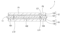
FIG. 1 is a plan view of an
絶縁回路基板1は、図1に示すように、平面視で縦寸法70mm及び横寸法36mmの矩形状に形成されている。このような絶縁回路基板1は、図2~4に示すように、セラミックス基板11と、セラミックス基板11の一方の面に形成された回路層12と、セラミックス基板11の他方の面に形成された金属層13とを備えている。これら回路層12及び金属層13は、セラミックス基板11よりも若干小さい矩形板状に形成されている。
As shown in FIG. 1, the
セラミックス基板11は、窒化アルミニウム(AlN)、窒化珪素(Si3N4)、アルミナ(Al2O3)等からなるセラミックス材料により形成され、厚さが0.3mm~1.0mmとされている。また、セラミックス基板11は、平面視で矩形板状に形成され、回路層12及び金属層13のそれぞれよりも若干大きく形成されている。また、セラミックス基板11は、複数の第1分割溝L1により3つのセラミックス片101~103に分割されている。これら第1分割溝L1は、絶縁回路基板1の幅方向に沿って横断するように形成され、各第1分割溝L1は、相互に平行に形成されている。
The
回路層12は、セラミックス基板11に形成されたアルミニウム又はアルミニウム合金からなる第1アルミニウム層121と、第1アルミニウム層121に固相拡散接合された銅又は銅合金からなる第1銅層122と、を有している。この回路層12は、第2分割溝L2により複数(3つ)の回路パターンP1~P3に分割されている。例えば、図1に示すように、矩形状の回路パターンP2と、回路パターンP2の三方を囲む回路パターンP1と、回路パターンP1の端部と間隔をあけて配置される矩形状の回路パターンP3とに、第2分割溝L2により分割されている。
The
金属層13は、セラミックス基板11に形成されたアルミニウム又はアルミニウム合金からなる第2アルミニウム層131と、第2アルミニウム層131に固相拡散接合された銅又は銅合金からなる第2銅層132と、を有している。これらのうち、第2アルミニウム層131は、セラミックス基板11とともに第1分割溝L1により分割されている。一方、第2銅層132は、第1分割溝L1及び第2分割溝L2のいずれにも分割されることがない。すなわち、1枚の銅板として存在している。
The
また、第1アルミニウム層121及び第2アルミニウム層131の厚さは、0.2mm以上0.6mm以下に設定され、第1銅層122及び第2銅層132の厚さは、0.8mm以上3.0mm以下に設定されている。これらのうち、第1銅層122の厚さが0.8mm未満であると、第2分割溝L2により分断された回路層12の複数の回路パターンP1~P3に生じる熱応力が小さいため、上記対策を施す必要性が乏しい。一方、第1銅層122の厚さが3.0mmを超えると、複数の回路パターンP1~P3に生じる熱応力が大きいため、第1アルミニウム層121を介してセラミックス基板11に固定されたとしても、各回路パターンP1~P3の略中央においてセラミックス基板11に割れが生じる可能性がある。
The thickness of the
[第1分割溝の構成]
第1分割溝L1は、セラミックス基板11の辺に平行に形成されている。この第1分割溝L1は、例えば、図1の破線に示す位置に形成され、セラミックス基板11を3つのセラミックス片101~103に分割する。この第1分割溝L1は、回路層12を回路パターンP1と回路パターンP2とに分割する第2分割溝L2の一部と重なって配置されるとともに、回路層12を回路パターンP2と回路パターンP3とに分割する第2分割溝L2と重なっている。これらのうち、回路層12の第2分割溝L2と重なって配置される部分を重複部分L11とし、第2分割溝L2と重なっていない部分を単独部分L12とする。単独部分L12は、第2分割溝L2とは異なる部位に重複部分L11を延長して形成される。本実施形態では、図1~図3に示すように、回路層12を回路パターンP1と回路パターンP2とに分割する第2分割溝L2の一部は、セラミックス基板11をセラミックス片101とセラミックス片102とに分割する第1分割溝L1の重複部分L11に重なって配置され、回路層12を回路パターンP1と回路パターンP3とに分割する第2分割溝L2は、セラミックス基板11をセラミックス片102とセラミックス片103とに分割する第1分割溝L1の重複部分L11に重なって配置されている。
[Structure of First Divided Groove]
The first dividing groove L1 is formed parallel to the sides of the
また、第1分割溝L1の単独部分L12においては、図3に示すように、その分割溝に沿って第1アルミニウム層121が分割され、第1銅層122は、該分割溝上にまたがって配置されている。すなわち、セラミックス基板11におけるセラミックス片101とセラミックス片102とを分割する第1分割溝L1上では、図3に示すように、セラミックス基板11、第1アルミニウム層121及び第2アルミニウム層131は、第1分割溝L1の単独部分L12により分割されているが、回路パターンP1を構成する第1銅層122は、単独部分L12において、分割されていない。
3, the
[絶縁回路基板の製造方法]
次に、以上のように構成される絶縁回路基板1の製造方法について説明する。この製造方法は、セラミックス基板11にスクライブライン111を形成し、そのセラミックス基板11に各アルミニウム板121A,131Aを接合した後、複数のセラミックス片101~103に分割する分割工程と、分割工程後に第2銅板132A上に各セラミックス片101~103を配置し、その上に第1銅板122Aを重ねて積層体とし、この積層体を加圧加熱することにより接合する接合工程と、を備える(図5参照)。また、接合工程は、スクライブライン形成工程、アルミニウム層形成工程及び個片化工程と、を有している。
以下、各工程のそれぞれについて、工程順に説明する。
[Manufacturing method of insulated circuit board]
Next, a method for manufacturing the insulating
Each step will be described below in the order of steps.
[スクライブライン形成工程]
まず、図5(a)に示すように、セラミックス基板11(縦70mm×横36mm)の一方の面(回路層12が形成される側の面)に、各セラミックス片101~103を分割するためのスクライブライン111を形成する。このスクライブライン111は、例えば、レーザ光を照射することにより、セラミックス基板11の一方の面を線状に除去して形成される。これらスクライブライン111は、セラミックス基板11に形成される溝部であり、セラミックス基板11の分割の起点となる。なお、スクライブライン111の加工は、例えばCO2レーザ、YAGレーザ、YVO4レーザ、YLFレーザ等によっても加工可能である。
[Scribing line forming process]
First, as shown in FIG. 5(a), on one side (the side on which the
[アルミニウム層形成工程]
次に、スクライブライン111が形成されたセラミックス基板11の一方の面に第1アルミニウム層121を形成し、他方の面に第2アルミニウム層131を形成する。具体的には、セラミックス基板11を洗浄液等により洗浄した後、第1アルミニウム層121となる第1アルミニウム板121Aを配置し、他方の面に第2アルミニウム層131となる第2アルミニウム板131Aを配置し、ろう材を介して接合した後、これらの積層体をカーボン板により挟持し、積層方向に荷重をかけながら真空中で加熱することにより、セラミックス基板11と各アルミニウム板121A,131Aを接合する。
[Aluminum layer forming step]
Next, a
[個片化工程]
そして、図5(b)に示すように、セラミックス基板11をスクライブライン111により分割して複数のセラミックス片101~103とする。また、この際、第1分割溝L1の一部と重なって配置される第2分割溝L2により第1アルミニウム層121を分割して複数のパターンを、例えば、エッチング等により形成する。
なお、これら複数のパターン形成は、エッチングにより行うこととしたが、第2分割溝L2により予め複数のパターンに分断された第1アルミニウム板121Aを接合することにより形成してもよい。
[Singulation process]
Then, as shown in FIG. 5B, the
Although the formation of the plurality of patterns is performed by etching, the patterns may be formed by bonding the
[接合工程]
分割工程後、複数のセラミックス片101~103を図5(c)に示すように、第2銅層132となる第2銅板132A上に間隔を開けて配置する。そして、複数のセラミックス片101~103の上面に第2分割溝L2により分割されて第1アルミニウム層121の複数のパターンと同形状の複数のパターンに分断された第1銅層122となる第1銅板122Aを配置する。この際、第1分割溝L1の単独部分L12においては、第1銅板122Aは、分割溝L1上にまたがって配置される。そして、この積層体を加圧及び加熱することにより第1アルミニウム板121A及び第1銅板122A、並びに第2アルミニウム板131A及び第2銅板132Aを固相拡散接合させて、絶縁回路基板1を製造する。
[Joining process]
After the dividing step, the plurality of
本実施形態では、回路層12を複数の回路パターンに分割する第2分割溝L2とは異なる部位に第1分割溝L1の単独部分L12が形成され、当該単独部分L12においては第1アルミニウム層121が分断されているので、複数の回路パターンに熱伸縮が生じても、セラミックス基板11に熱応力が生じにくい。したがって、加熱時の反り変化によってセラミックス基板11が割れることを抑制できる。また、第1分割溝L1がセラミックス基板11の辺に平行に形成されているので、当該絶縁回路基板1を製造するのが容易となる。さらに、第1銅層の厚さが0.8mm以上3.0mm以下とされているので、セラミックス基板11に割れが生じる可能性を抑制できる。
In the present embodiment, a single portion L12 of the first dividing groove L1 is formed at a location different from the second dividing groove L2 that divides the
なお、本発明は上記実施形態に限定されることはなく、本発明の趣旨を逸脱しない範囲において種々の変更を加えることが可能である。
例えば、上記実施形態では、第2分割溝L2により3つの回路パターンP1~P3に分割されることとしたが、これに限らず、回路パターンは、適宜変更できる。図6は、上記実施形態の第1変形例に係る絶縁回路基板1Aを回路層12A側から見た平面図である。
この絶縁回路基板1Aの回路層12Aは、図6に示すように、第2分割溝L2により複数(5つ)の回路パターンP4~P8に分割されている。例えば、図6に示すように、第2分割溝L2は、絶縁回路基板1Aの幅方向を直線で横断するものではなく、複数回屈曲したり、枠状に各回路パターンP6~P8を囲んだりする形状である。これら第2分割溝L2は、回路層12A(セラミックス基板11)の辺に平行に延びるとともに、複雑に入り組んでいる。このような第2分割溝L2により分断された回路パターンP6,P7,P8は、矩形状に形成されている。
The present invention is not limited to the above embodiments, and various modifications can be made without departing from the scope of the present invention.
For example, in the above embodiment, the second dividing groove L2 divides the circuit pattern into three circuit patterns P1 to P3. FIG. 6 is a plan view of an insulated
As shown in FIG. 6, the
なお、第1分割溝L1は、第1実施形態の第1分割溝L1と同じ位置に配置され、これらの一部は、第2分割溝L2と重なっている。具体的には、回路層12Aを回路パターンP4と回路パターンP5とに分割する第2分割溝L2の一部と、セラミックス基板11をセラミックス片101とセラミックス片102とに分割する第1分割溝L1の重複部分L11とが重なって配置されている。また、回路層12Aを回路パターンP6,P7と回路パターンP5,P8とに分割する第2分割溝L2の一部と、セラミックス基板11をセラミック片102とセラミックス片103とに分割する第1分割溝L1の重複部分L11とが重なって配置されている。
The first dividing grooves L1 are arranged at the same positions as the first dividing grooves L1 of the first embodiment, and part of them overlaps the second dividing grooves L2. Specifically, a part of the second dividing groove L2 that divides the
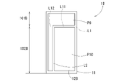
図7は、上記実施形態の第2変形例に係る絶縁回路基板1Bを回路層12B側から見た平面図である。
この絶縁回路基板1Bの回路層12Bは、図7に示すように、第2分割溝L2により複数(2つ)の回路パターンP9,P10に分割されている。例えば、図7に示すように、回路層12BにL字状に形成され、回路層12Bを矩形状の回路パターンP10と、矩形状の回路層12Bの一部を矩形状に切欠いた形状の回路パターンP9とに分割する第2分割溝L2が形成されている。この第2分割溝L2は、回路層12B(セラミックス基板11)の辺に平行に延びている。
FIG. 7 is a plan view of an insulated circuit board 1B according to a second modification of the above embodiment, viewed from the
As shown in FIG. 7, the
この第1分割溝L1は、セラミックス基板11を横方向に分断する直線状に形成され、その一部が、第2分割溝L2と重なっている。具体的には、回路層12Bを回路パターンP9と回路パターンP10とに分割する第2分割溝L2の横方向に延びる部分と、セラミックス基板11をセラミックス片101Bとセラミックス片102Bとに分割する第1分割溝L1の重複部分L11とが重なって配置されている。
The first dividing groove L1 is formed in a straight line that divides the
上述した第1変形例及び第2変形例のいずれにおいても、セラミックス基板11が分割されているので、回路層12A,12Bを複数の回路パターンに分割する第2分割溝L2とは異なる部位に第1分割溝L1の単独部分L12が形成され、当該単独部分L12においては第1アルミニウム層121が分断されているので、複数の回路パターンに熱伸縮が生じても、セラミックス基板11に熱応力が生じにくい。したがって、加熱時の反り変化によってセラミックス基板11が割れることを抑制できる。
In both the first modified example and the second modified example described above, the
上記実施形態では、第1分割溝L1は、セラミックス基板11の辺に平行に形成されていることとしたが、これに限らない。セラミックス基板11の辺に交差する方向に形成されていてもよい。すなわち、セラミックス基板11の割れを抑制できれば、いずれの位置に形成されていてもよい。
In the above embodiment, the first dividing grooves L1 are formed parallel to the sides of the
上記実施形態では、第1分割溝L1により、セラミックス基板11、第1アルミニウム層121及び第2アルミニウム層131が分割されていることとしたが、これに限らず、第2アルミニウム層131は、分割されていなくてもよい。
In the above embodiment, the
1 1A 1B 絶縁回路基板
11 セラミックス基板
12 12A 12B 回路層
121 第1アルミニウム層
122 第1銅層
13 金属層
131 第2アルミニウム層
132 第2アルミニウム層
101 102 103 101A 102B セラミックス片
P1 P2 P3 P4 P5 P6 P7 P8 P9 P10 回路パターン
L1 第1分割溝
L11 重複部分
L12 単独部分
L2 第2分割溝
1 1A 1B
Claims (4)
前記回路層は、前記セラミックス基板に形成されたアルミニウム又はアルミニウム合金からなる第1アルミニウム層と、前記第1アルミニウム層に固相拡散接合された銅又は銅合金からなる第1銅層と、を有し、
前記セラミックス基板は、第1分割溝により複数のセラミックス片に分割されるとともに、前記回路層は、第2分割溝により複数の回路パターンに分割され、
前記セラミックス基板の第1分割溝は、前記回路層の第2分割溝と重なって配置される重複部分と、前記第2分割溝とは異なる部位に前記重複部分を延長して形成される単独部分と、を有し、
前記単独部分においては、その分割溝に沿って前記第1アルミニウム層が分割され、前記第1銅層は、該分割溝上にまたがって配置されていることを特徴とする絶縁回路基板。 An insulated circuit board having a circuit layer formed on one surface of a ceramic substrate and a metal layer formed on the other surface of the ceramic substrate,
The circuit layer has a first aluminum layer made of aluminum or an aluminum alloy formed on the ceramic substrate, and a first copper layer made of copper or a copper alloy solid phase diffusion bonded to the first aluminum layer. death,
The ceramic substrate is divided into a plurality of ceramic pieces by first dividing grooves, and the circuit layer is divided into a plurality of circuit patterns by second dividing grooves,
The first dividing groove of the ceramic substrate includes an overlapping portion arranged to overlap with the second dividing groove of the circuit layer, and a single portion formed by extending the overlapping portion to a location different from the second dividing groove. and
In the isolated circuit board, the first aluminum layer is divided along the dividing groove in the independent portion, and the first copper layer is arranged over the dividing groove.
前記セラミックス基板の一方の面に前記第1アルミニウム層を接合するとともに、前記セラミックス基板の他方の面に前記第2アルミニウム層を接合した後、前記セラミックス基板を第1分割溝により分割して複数のセラミックス片を形成するとともに、前記第1分割溝の一部と重なって配置される第2分割溝により前記第1アルミニウム層を分割して複数のパターンを形成する分割工程と、
前記分割工程後に、複数の前記セラミックス片のそれぞれを前記第2銅層上に間隔を開けて配置するとともに、複数の前記セラミックス片の上面に前記第1銅層を重ねて積層体を形成し、前記積層体を加圧及び加熱することにより前記第1アルミニウム層及び前記第1銅層、並びに前記第2アルミニウム層及び前記第2銅層を固相拡散接合させる接合工程と、を備え、
前記分割工程における前記セラミックス基板を分割する前記第1分割溝は、前記第2分割溝と重なって配置される重複部分と、前記第2分割溝とは異なる部位に前記重複部分を延長して形成される単独部分と、を有し、
前記接合工程における前記第1銅層は、前記第1アルミニウム層の複数のパターンと同じ複数のパターンに分断されており、その少なくとも一つは、前記単独部分において、その分割溝上にまたがって配置されて接合されることを特徴とする絶縁回路基板の製造方法。 A circuit layer comprising a first aluminum layer made of aluminum or an aluminum alloy and a first copper layer made of copper or a copper alloy solid phase diffusion bonded to the first aluminum layer is formed on one surface of a ceramic substrate, A metal layer comprising a second aluminum layer made of aluminum or an aluminum alloy and a second copper layer made of copper or a copper alloy solid phase diffusion bonded to the second aluminum layer is formed on the other surface of the ceramic substrate. A method for manufacturing an insulated circuit board comprising:
After bonding the first aluminum layer to one surface of the ceramic substrate and bonding the second aluminum layer to the other surface of the ceramic substrate, the ceramic substrate is divided by first dividing grooves into a plurality of a dividing step of forming a ceramic piece and dividing the first aluminum layer by a second dividing groove arranged to overlap a part of the first dividing groove to form a plurality of patterns;
After the dividing step, each of the plurality of ceramic pieces is arranged on the second copper layer with a gap therebetween, and the first copper layer is overlapped on the upper surface of the plurality of ceramic pieces to form a laminate, a bonding step of solid-phase diffusion bonding the first aluminum layer and the first copper layer, and the second aluminum layer and the second copper layer by applying pressure and heat to the laminate,
The first dividing groove for dividing the ceramic substrate in the dividing step is formed by extending an overlapping portion arranged to overlap with the second dividing groove and extending the overlapping portion to a location different from the second dividing groove. and
The first copper layer in the bonding step is divided into a plurality of patterns that are the same as the plurality of patterns of the first aluminum layer, and at least one of the patterns is arranged across the dividing groove in the single portion. A method for manufacturing an insulated circuit board, characterized in that the substrates are joined together by
Priority Applications (1)
| Application Number | Priority Date | Filing Date | Title |
|---|---|---|---|
| JP2019022284A JP7147610B2 (en) | 2019-02-12 | 2019-02-12 | Insulated circuit board and its manufacturing method |
Applications Claiming Priority (1)
| Application Number | Priority Date | Filing Date | Title |
|---|---|---|---|
| JP2019022284A JP7147610B2 (en) | 2019-02-12 | 2019-02-12 | Insulated circuit board and its manufacturing method |
Publications (2)
| Publication Number | Publication Date |
|---|---|
| JP2020129631A JP2020129631A (en) | 2020-08-27 |
| JP7147610B2 true JP7147610B2 (en) | 2022-10-05 |
Family
ID=72174798
Family Applications (1)
| Application Number | Title | Priority Date | Filing Date |
|---|---|---|---|
| JP2019022284A Active JP7147610B2 (en) | 2019-02-12 | 2019-02-12 | Insulated circuit board and its manufacturing method |
Country Status (1)
| Country | Link |
|---|---|
| JP (1) | JP7147610B2 (en) |
Families Citing this family (1)
| Publication number | Priority date | Publication date | Assignee | Title |
|---|---|---|---|---|
| KR20230097341A (en) * | 2021-12-24 | 2023-07-03 | 주식회사 엘엑스세미콘 | Method for manufacturing circuit board |
Citations (4)
| Publication number | Priority date | Publication date | Assignee | Title |
|---|---|---|---|---|
| JP2003078086A (en) | 2001-09-04 | 2003-03-14 | Kubota Corp | Lamination structure of semiconductor module substrate |
| JP2009158502A (en) | 2007-12-25 | 2009-07-16 | Toyota Motor Corp | Semiconductor module |
| JP2016027645A (en) | 2014-07-04 | 2016-02-18 | 三菱マテリアル株式会社 | Board for power module with heat radiation plate and power module |
| JP2018137396A (en) | 2017-02-23 | 2018-08-30 | 三菱マテリアル株式会社 | Manufacturing method of substrate for power module |
Family Cites Families (1)
| Publication number | Priority date | Publication date | Assignee | Title |
|---|---|---|---|---|
| CN106463477B (en) * | 2014-07-04 | 2019-03-12 | 三菱综合材料株式会社 | Power module substrate unit and power module |
-
2019
- 2019-02-12 JP JP2019022284A patent/JP7147610B2/en active Active
Patent Citations (4)
| Publication number | Priority date | Publication date | Assignee | Title |
|---|---|---|---|---|
| JP2003078086A (en) | 2001-09-04 | 2003-03-14 | Kubota Corp | Lamination structure of semiconductor module substrate |
| JP2009158502A (en) | 2007-12-25 | 2009-07-16 | Toyota Motor Corp | Semiconductor module |
| JP2016027645A (en) | 2014-07-04 | 2016-02-18 | 三菱マテリアル株式会社 | Board for power module with heat radiation plate and power module |
| JP2018137396A (en) | 2017-02-23 | 2018-08-30 | 三菱マテリアル株式会社 | Manufacturing method of substrate for power module |
Also Published As
| Publication number | Publication date |
|---|---|
| JP2020129631A (en) | 2020-08-27 |
Similar Documents
| Publication | Publication Date | Title |
|---|---|---|
| JP6100605B2 (en) | Manufacturing method of multilayer clad material | |
| US11908768B2 (en) | Method of manufacturing bonded body for insulation circuit substrate board and bonded body for insulation circuit substrate board | |
| JP6853455B2 (en) | Manufacturing method of board for power module | |
| JP2008010520A (en) | Substrate for power module, and its manufacturing method | |
| JP7147610B2 (en) | Insulated circuit board and its manufacturing method | |
| JP5817164B2 (en) | Joining method, joining jig | |
| TWI762771B (en) | Insulated circuit board | |
| WO2019198551A1 (en) | Ceramics-metal bonded body and method of manufacturing same, and multi-piece ceramics-metal bonded body and method of manufacturing same | |
| JP2019009333A (en) | Manufacturing method of ceramic-metal conjugate, manufacturing method of ceramic circuit board and ceramic-metal conjugate | |
| TWI770346B (en) | Method for manufacturing power module substrate and ceramic-copper joint | |
| KR102365887B1 (en) | Adapter elements for connecting components such as laser diodes to heat sinks, systems including laser diodes, heat sinks, and adapter elements, and methods of manufacturing adapter elements | |
| JP7415486B2 (en) | Insulated circuit board with heat sink and method for manufacturing the same | |
| JP3975862B2 (en) | Power module substrate and manufacturing method thereof | |
| JP7467936B2 (en) | Heat sink-equipped insulating circuit board, electronic components, and method for manufacturing the heat sink-equipped insulating circuit board | |
| JP7230602B2 (en) | Insulated circuit board and its manufacturing method | |
| JP5303936B2 (en) | Power module substrate, power module, and method of manufacturing power module substrate | |
| WO2019188884A1 (en) | Insulated circuit board with heat sink | |
| JP6201384B2 (en) | Multilayer substrate for power module manufacturing | |
| JP2019127408A (en) | Manufacturing method for ceramic-metal joint material, manufacturing apparatus and ceramic-metal joint material | |
| JP2018129485A (en) | Semiconductor device | |
| JP2009016592A (en) | Ceramic wiring board |
Legal Events
| Date | Code | Title | Description |
|---|---|---|---|
| A621 | Written request for application examination |
Free format text: JAPANESE INTERMEDIATE CODE: A621 Effective date: 20210930 |
|
| A977 | Report on retrieval |
Free format text: JAPANESE INTERMEDIATE CODE: A971007 Effective date: 20220815 |
|
| TRDD | Decision of grant or rejection written | ||
| A01 | Written decision to grant a patent or to grant a registration (utility model) |
Free format text: JAPANESE INTERMEDIATE CODE: A01 Effective date: 20220823 |
|
| A61 | First payment of annual fees (during grant procedure) |
Free format text: JAPANESE INTERMEDIATE CODE: A61 Effective date: 20220905 |
|
| R150 | Certificate of patent or registration of utility model |
Ref document number: 7147610 Country of ref document: JP Free format text: JAPANESE INTERMEDIATE CODE: R150 |