JP7143638B2 - Method for manufacturing silicon carbide epitaxial substrate - Google Patents

Method for manufacturing silicon carbide epitaxial substrate Download PDF

Info

Publication number
JP7143638B2
JP7143638B2 JP2018111994A JP2018111994A JP7143638B2 JP 7143638 B2 JP7143638 B2 JP 7143638B2 JP 2018111994 A JP2018111994 A JP 2018111994A JP 2018111994 A JP2018111994 A JP 2018111994A JP 7143638 B2 JP7143638 B2 JP 7143638B2
Authority
JP
Japan
Prior art keywords
silicon carbide
main surface
substrate
carbide substrate
etching
Prior art date
Legal status (The legal status is an assumption and is not a legal conclusion. Google has not performed a legal analysis and makes no representation as to the accuracy of the status listed.)
Active
Application number
JP2018111994A
Other languages
Japanese (ja)
Other versions
JP2019216166A (en
Inventor
勉 堀
圭司 和田
貴也 宮瀬
Current Assignee (The listed assignees may be inaccurate. Google has not performed a legal analysis and makes no representation or warranty as to the accuracy of the list.)
Sumitomo Electric Industries Ltd
Original Assignee
Sumitomo Electric Industries Ltd
Priority date (The priority date is an assumption and is not a legal conclusion. Google has not performed a legal analysis and makes no representation as to the accuracy of the date listed.)
Filing date
Publication date
Application filed by Sumitomo Electric Industries Ltd filed Critical Sumitomo Electric Industries Ltd
Priority to JP2018111994A priority Critical patent/JP7143638B2/en
Publication of JP2019216166A publication Critical patent/JP2019216166A/en
Application granted granted Critical
Publication of JP7143638B2 publication Critical patent/JP7143638B2/en
Active legal-status Critical Current
Anticipated expiration legal-status Critical

Links

Images

Description

本開示は、炭化珪素エピタキシャル基板の製造方法に関する。 The present disclosure relates to a method for manufacturing a silicon carbide epitaxial substrate.

特開2014-170891号公報(特許文献1)には、炭化珪素単結晶基板上に炭化珪素層をエピタキシャル成長させる方法が開示されている。 Japanese Patent Application Laid-Open No. 2014-170891 (Patent Document 1) discloses a method of epitaxially growing a silicon carbide layer on a silicon carbide single crystal substrate.

特開2014-170891号公報JP 2014-170891 A

炭化珪素単結晶基板上に炭化珪素層をエピタキシャル成長させる際、炭化珪素基板に残留応力がある場合、炭化珪素基板に割れが発生することがある。 When a silicon carbide layer is epitaxially grown on a silicon carbide single crystal substrate, cracks may occur in the silicon carbide substrate if the silicon carbide substrate has residual stress.

本開示の目的の一つは、エピタキシャル成長させる際の割れ発生を抑制可能な炭化珪素エピタキシャル基板の製造方法を提供することである。 One object of the present disclosure is to provide a method for manufacturing a silicon carbide epitaxial substrate that can suppress the occurrence of cracks during epitaxial growth.

本開示に係る炭化珪素エピタキシャル基板の製造方法は、以下の工程を備えている。主表面を有する炭化珪素基板が反応室に導入される。反応室において、主表面の全面が平均値で0.7μm以上10μm以下エッチングされる。エッチングする工程後、反応室において、主表面上に炭化珪素エピタキシャル膜が形成される。 A method for manufacturing a silicon carbide epitaxial substrate according to the present disclosure includes the following steps. A silicon carbide substrate having a major surface is introduced into the reaction chamber. In the reaction chamber, the entire main surface is etched by an average value of 0.7 μm to 10 μm. After the etching step, a silicon carbide epitaxial film is formed on the main surface in the reaction chamber.

上記の製造方法によれば、エピタキシャル成長させる際の割れ発生を抑制可能である。 According to the manufacturing method described above, it is possible to suppress the occurrence of cracks during epitaxial growth.

図1は、本実施形態に係る炭化珪素エピタキシャル基板の構成を示す平面模式図である。FIG. 1 is a schematic plan view showing the configuration of a silicon carbide epitaxial substrate according to this embodiment. 図2は、本実施形態に係る炭化珪素エピタキシャル基板の構成を示す断面模式図である。FIG. 2 is a schematic cross-sectional view showing the configuration of the silicon carbide epitaxial substrate according to this embodiment. 図3は、本実施形態に係る炭化珪素エピタキシャル基板の製造装置の構成を示す一部断面模式図である。FIG. 3 is a schematic partial cross-sectional view showing the configuration of the silicon carbide epitaxial substrate manufacturing apparatus according to the present embodiment. 図4は、本実施形態に係る炭化珪素エピタキシャル基板の製造方法を概略的に示すフローチャートである。FIG. 4 is a flow chart schematically showing a method for manufacturing a silicon carbide epitaxial substrate according to this embodiment. 図5は、本実施形態に係る炭化珪素エピタキシャル基板の製造方法における温度と時間との関係を示す図である。FIG. 5 is a diagram showing the relationship between temperature and time in the method for manufacturing a silicon carbide epitaxial substrate according to this embodiment. 図6は、エッチング量の測定位置を示す図である。FIG. 6 is a diagram showing positions where the etching amount is measured. 図7は、エッチング量と測定位置との関係を示す図である。FIG. 7 is a diagram showing the relationship between the etching amount and the measurement position.

[本開示の実施形態の概要]
まず本開示の実施形態の概要について説明する。本明細書の結晶学的記載においては、個別方位を[]、集合方位を<>、個別面を()、集合面を{}でそれぞれ示す。結晶学上の指数が負であることは、通常、数字の上に”-”(バー)を付すことによって表現されるが、本明細書では数字の前に負の符号を付すことによって結晶学上の負の指数を表現する。
[Outline of Embodiment of Present Disclosure]
First, an outline of an embodiment of the present disclosure will be described. In the crystallographic description of this specification, individual orientations are indicated by [ ], collective orientations by <>, individual planes by ( ), and collective planes by { }. Negative crystallographic exponents are usually expressed by placing a "-" (bar) above the number, but here the crystallographic index is expressed by prefixing the number with a negative sign. Represents a negative exponent above.

(1)本開示に係る炭化珪素エピタキシャル基板100の製造方法は、以下の工程を備えている。主表面11を有する炭化珪素基板10が反応室201に導入される。反応室201において、主表面11の全面が平均値で0.7μm以上10μm以下エッチングされる。エッチングする工程後、反応室201において、主表面11上に炭化珪素エピタキシャル膜20が形成される。 (1) A method for manufacturing silicon carbide epitaxial substrate 100 according to the present disclosure includes the following steps. Silicon carbide substrate 10 having main surface 11 is introduced into reaction chamber 201 . In the reaction chamber 201, the entire surface of the main surface 11 is etched by an average value of 0.7 μm to 10 μm. After the etching step, silicon carbide epitaxial film 20 is formed on main surface 11 in reaction chamber 201 .

(2)上記(1)に係る炭化珪素エピタキシャル基板100の製造方法において、主表面11の全面をエッチングする工程においては、水素を含むガスが使用されてもよい。 (2) In the method for manufacturing silicon carbide epitaxial substrate 100 according to (1) above, a gas containing hydrogen may be used in the step of etching the entire surface of main surface 11 .

(3)上記(2)に係る炭化珪素エピタキシャル基板100の製造方法において、主表面11の全面をエッチングする工程においては、炭化珪素基板10の温度は、1600℃以上2000℃以下であってもよい。 (3) In the method for manufacturing silicon carbide epitaxial substrate 100 according to (2) above, in the step of etching the entire main surface 11, the temperature of silicon carbide substrate 10 may be 1600° C. or more and 2000° C. or less. .

(4)上記(1)に係る炭化珪素エピタキシャル基板100の製造方法において、主表面11の全面をエッチングする工程においては、ハロゲンを含むガスが使用されてもよい。 (4) In the method for manufacturing silicon carbide epitaxial substrate 100 according to (1) above, gas containing halogen may be used in the step of etching the entire surface of main surface 11 .

(5)上記(4)に係る炭化珪素エピタキシャル基板100の製造方法において、主表面11の全面をエッチングする工程においては、炭化珪素基板10の温度は、1600℃以上2000℃以下であってもよい。 (5) In the method for manufacturing silicon carbide epitaxial substrate 100 according to (4) above, in the step of etching the entire main surface 11, the temperature of silicon carbide substrate 10 may be 1600° C. or more and 2000° C. or less. .

(6)上記(1)に係る炭化珪素エピタキシャル基板100の製造方法において、主表面11の全面をエッチングする工程においては、主表面11において、炭化珪素が昇華してもよい。 (6) In the method for manufacturing silicon carbide epitaxial substrate 100 according to (1) above, in the step of etching the entire surface of main surface 11 , silicon carbide may sublime on main surface 11 .

(7)上記(6)に係る炭化珪素エピタキシャル基板100の製造方法において、主表面11の全面をエッチングする工程においては、炭化珪素基板10の温度は、1700℃以上2200℃以下であってもよい。 (7) In the method for manufacturing silicon carbide epitaxial substrate 100 according to (6) above, in the step of etching the entire main surface 11, the temperature of silicon carbide substrate 10 may be 1700° C. or more and 2200° C. or less. .

(8)上記(1)~(7)のいずれかに係る炭化珪素エピタキシャル基板100の製造方法によれば、エッチングする工程において、主表面11内における炭化珪素基板10のエッチング量の標準偏差を、主表面11内におけるエッチング量の平均値で除した値は、15%以下であってもよい。 (8) According to the method for manufacturing silicon carbide epitaxial substrate 100 according to any one of (1) to (7) above, in the step of etching, the standard deviation of the etching amount of silicon carbide substrate 10 within main surface 11 is The value obtained by dividing the etching amount in the main surface 11 by the average value may be 15% or less.

[本開示の実施形態の詳細]
以下、本開示の実施形態の詳細について説明する。以下の説明では、同一または対応する要素には同一の符号を付し、それらについて同じ説明は繰り返さない。
[Details of the embodiment of the present disclosure]
Details of the embodiments of the present disclosure will be described below. In the following description, the same or corresponding elements are given the same reference numerals and the same descriptions thereof are not repeated.

(炭化珪素エピタキシャル基板)
図1に示されるように、本実施形態に係る炭化珪素エピタキシャル基板100は、炭化珪素基板10と、炭化珪素エピタキシャル膜20とを有している。炭化珪素基板10は、第1主面11と、第1主面11と反対側の第3主面13とを含む。炭化珪素エピタキシャル膜20は、炭化珪素基板10上にある。炭化珪素エピタキシャル膜20は、炭化珪素基板10と接する第4主面14と、第4主面14と反対側の第2主面12(主表面12)を含む。図1に示されるように、炭化珪素エピタキシャル基板100には、第1方向101に延在する第1フラット16が設けられて入れてもよい。炭化珪素エピタキシャル基板100には、第2方向102に延在する第2フラット(図示せず)が設けられていてもよい。
(Silicon carbide epitaxial substrate)
As shown in FIG. 1 , silicon carbide epitaxial substrate 100 according to the present embodiment has silicon carbide substrate 10 and silicon carbide epitaxial film 20 . Silicon carbide substrate 10 includes a first main surface 11 and a third main surface 13 opposite to first main surface 11 . Silicon carbide epitaxial film 20 is on silicon carbide substrate 10 . Silicon carbide epitaxial film 20 includes a fourth main surface 14 in contact with silicon carbide substrate 10 and a second main surface 12 (main surface 12 ) opposite to fourth main surface 14 . As shown in FIG. 1, a silicon carbide epitaxial substrate 100 may be provided with a first flat 16 extending in a first direction 101 . Silicon carbide epitaxial substrate 100 may be provided with a second flat (not shown) extending in second direction 102 .

第1方向101は、第2主面12に対して平行であり、かつ第2方向102に対して垂直な方向である。第2方向102は、たとえば<1-100>方向である。図1に示されるように、第2主面12の最大径111(直径)は、たとえば100mm以上である。最大径111は150mm以上でもよいし、200mm以上でもよいし、250mm以上でもよい。最大径111の上限は特に限定されない。最大径111の上限は、たとえば300mmであってもよい。 The first direction 101 is parallel to the second major surface 12 and perpendicular to the second direction 102 . The second direction 102 is, for example, the <1-100> direction. As shown in FIG. 1, the maximum diameter 111 (diameter) of the second main surface 12 is, for example, 100 mm or more. The maximum diameter 111 may be 150 mm or more, 200 mm or more, or 250 mm or more. The upper limit of the maximum diameter 111 is not particularly limited. The upper limit of the maximum diameter 111 may be 300 mm, for example.

炭化珪素基板10は、炭化珪素単結晶から構成される。炭化珪素単結晶のポリタイプは、たとえば4Hである。ポリタイプ4Hは、電子移動度、絶縁破壊電界強度等において他のポリタイプより優れている。炭化珪素基板10は、たとえば窒素(N)などのn型不純物を含んでいる。炭化珪素基板10の導電型は、たとえばn型である。第1主面11は、たとえば{0001}面から8°以下の角度だけ傾斜した面である。第1主面11が{0001}面から傾斜している場合、第1主面11の法線の傾斜方向は、たとえば<11-20>方向である。 Silicon carbide substrate 10 is made of silicon carbide single crystal. The polytype of silicon carbide single crystal is, for example, 4H. Polytype 4H is superior to other polytypes in terms of electron mobility, dielectric breakdown field strength, and the like. Silicon carbide substrate 10 contains n-type impurities such as nitrogen (N), for example. The conductivity type of silicon carbide substrate 10 is, for example, the n type. The first main surface 11 is, for example, a surface inclined at an angle of 8° or less from the {0001} plane. When first main surface 11 is inclined from the {0001} plane, the direction of inclination of the normal to first main surface 11 is, for example, the <11-20> direction.

図2に示されるように、炭化珪素エピタキシャル膜20は、炭化珪素基板10の第1主面11上にある。炭化珪素エピタキシャル膜20は、エピタキシャル層である。炭化珪素エピタキシャル膜20は、第1主面11に接している。炭化珪素エピタキシャル膜20は、たとえば窒素などのn型不純物を含んでいる。炭化珪素エピタキシャル膜20の導電型は、たとえばn型である。第2主面12は、たとえば{0001}面がオフ方向にオフ角だけ傾斜した面である。具体的には、第2主面12は、(0001)面がオフ方向に8°以下傾斜した面であってもよい。代替的に、第2主面12は、(000-1)面がオフ方向に8°以下傾斜した面であってもよい。 As shown in FIG. 2 , silicon carbide epitaxial film 20 is on first main surface 11 of silicon carbide substrate 10 . Silicon carbide epitaxial film 20 is an epitaxial layer. Silicon carbide epitaxial film 20 is in contact with first main surface 11 . Silicon carbide epitaxial film 20 contains n-type impurities such as nitrogen. The conductivity type of silicon carbide epitaxial film 20 is, for example, n-type. Second main surface 12 is, for example, a plane in which the {0001} plane is inclined by an off angle in the off direction. Specifically, the second main surface 12 may be a surface in which the (0001) plane is inclined by 8° or less in the off direction. Alternatively, the second main surface 12 may be a surface in which the (000-1) plane is inclined by 8° or less in the off direction.

オフ方向は、たとえば<11-20>方向である。なお、オフ方向は、<11-20>方向に限定されない。オフ方向は、たとえば<1-100>方向であってもよいし、<1-100>方向成分と<11-20>方向成分とを有する方向であってもよい。オフ角は、第2主面が{0001}面に対して傾斜している角度である。オフ角は、たとえば0°より大きく8°以下である。オフ角θは、1°以上であってもよいし、2°以上であってもよい。オフ角は、7°以下であってもよいし、6°以下であってもよい。 The off direction is, for example, the <11-20> direction. Note that the off direction is not limited to the <11-20> direction. The off direction may be, for example, the <1-100> direction, or may be a direction having a <1-100> direction component and a <11-20> direction component. The off angle is the angle at which the second main surface is inclined with respect to the {0001} plane. The off angle is, for example, greater than 0° and 8° or less. The off angle θ may be 1° or more, or may be 2° or more. The off angle may be 7° or less, or may be 6° or less.

炭化珪素エピタキシャル膜20は、たとえば窒素などのn型不純物を含んでいる。炭化珪素エピタキシャル膜20が含むn型不純物の濃度は、たとえば1×1015cm-3以上1×1019cm-3以下であってもよい。炭化珪素エピタキシャル膜20が含むn型不純物の濃度は、炭化珪素基板10が含むn型不純物の濃度よりも低くてもよい。炭化珪素エピタキシャル膜20の厚み114は、たとえば10μmである。炭化珪素エピタキシャル膜20の厚み114は、たとえば5μm以上50μm以下であってもよい。炭化珪素エピタキシャル膜20と炭化珪素基板10との間にバッファ層(図示せず)が設けられていてもよい。バッファ層は、たとえば窒素などのn型不純物を含んでいる。バッファ層のn型不純物の濃度は、炭化珪素エピタキシャル膜20のn型不純物の濃度よりも高くてもよい。バッファ層のn型不純物の濃度は、炭化珪素基板10のn型不純物の濃度よりも低くてもよい。 Silicon carbide epitaxial film 20 contains n-type impurities such as nitrogen. Silicon carbide epitaxial film 20 may have an n-type impurity concentration of, for example, 1×10 15 cm −3 or more and 1×10 19 cm −3 or less. The concentration of n-type impurities contained in silicon carbide epitaxial film 20 may be lower than the concentration of n-type impurities contained in silicon carbide substrate 10 . A thickness 114 of silicon carbide epitaxial film 20 is, for example, 10 μm. Silicon carbide epitaxial film 20 may have thickness 114 of, for example, 5 μm or more and 50 μm or less. A buffer layer (not shown) may be provided between silicon carbide epitaxial film 20 and silicon carbide substrate 10 . The buffer layer contains n-type impurities such as nitrogen. The n-type impurity concentration of the buffer layer may be higher than the n-type impurity concentration of silicon carbide epitaxial film 20 . The n-type impurity concentration of the buffer layer may be lower than the n-type impurity concentration of silicon carbide substrate 10 .

(炭化珪素エピタキシャル基板の製造装置)
次に、本実施形態に係る炭化珪素エピタキシャル基板100の製造装置200の構成について説明する。
(Manufacturing apparatus for silicon carbide epitaxial substrate)
Next, the configuration of manufacturing apparatus 200 for silicon carbide epitaxial substrate 100 according to the present embodiment will be described.

図3に示されるように、炭化珪素エピタキシャル基板100の製造装置200は、たとえばホットウォール方式の横型CVD(Chemical Vapor Deposition)装置である。製造装置200は、反応室201と、パイロメータ202と、発熱体203と、石英管204と、断熱材205と、誘導加熱コイル206とを主に有している。 As shown in FIG. 3, manufacturing apparatus 200 for silicon carbide epitaxial substrate 100 is, for example, a hot wall type horizontal CVD (Chemical Vapor Deposition) apparatus. The manufacturing apparatus 200 mainly has a reaction chamber 201 , a pyrometer 202 , a heating element 203 , a quartz tube 204 , a heat insulator 205 and an induction heating coil 206 .

発熱体203は、たとえば筒状の形状を有しており、内部に反応室201を形成している。発熱体203は、たとえば黒鉛製である。断熱材205は、発熱体203の外周を取り囲んでいる。断熱材205は、石英管204の内周面に接するように石英管204の内部に設けられている。誘導加熱コイル206は、たとえば石英管204の外周面に沿って巻回されている。誘導加熱コイル206は、外部電源(図示せず)により、交流電流が供給可能に構成されている。これにより、発熱体203が誘導加熱される。結果として、反応室201が発熱体203により加熱される。 Heating element 203 has, for example, a cylindrical shape, and forms reaction chamber 201 therein. The heating element 203 is made of graphite, for example. A heat insulating material 205 surrounds the outer circumference of the heating element 203 . The heat insulating material 205 is provided inside the quartz tube 204 so as to be in contact with the inner peripheral surface of the quartz tube 204 . The induction heating coil 206 is wound along the outer peripheral surface of the quartz tube 204, for example. The induction heating coil 206 is configured such that an alternating current can be supplied from an external power source (not shown). Thereby, the heating element 203 is induction-heated. As a result, reaction chamber 201 is heated by heating element 203 .

反応室201は、発熱体203に取り囲まれて形成された空間である。反応室201内には、炭化珪素基板10が配置される。反応室201は、炭化珪素基板10を加熱可能に構成されている。反応室201には、炭化珪素基板10を保持するサセプタ210が設けられている。サセプタ210は、回転軸212の周りを自転可能に構成されている。サセプタ210には、たとえば3枚の炭化珪素基板10が配置される。 A reaction chamber 201 is a space surrounded by a heating element 203 . Silicon carbide substrate 10 is arranged in reaction chamber 201 . Reaction chamber 201 is configured to be able to heat silicon carbide substrate 10 . Reaction chamber 201 is provided with a susceptor 210 that holds silicon carbide substrate 10 . The susceptor 210 is configured to be rotatable around a rotating shaft 212 . For example, three silicon carbide substrates 10 are arranged on susceptor 210 .

製造装置200は、ガス導入口207およびガス排気口208を有している。ガス排気口208は、排気ポンプ(図示せず)に接続されている。図6中の矢印は、ガスの流れを示している。ガスは、ガス導入口207から反応室201に導入され、ガス排気口208から排気される。反応室201内の圧力は、ガスの供給量と、ガスの排気量とのバランスによって調整される。 The manufacturing apparatus 200 has a gas inlet 207 and a gas outlet 208 . Gas exhaust port 208 is connected to an exhaust pump (not shown). Arrows in FIG. 6 indicate gas flows. A gas is introduced into the reaction chamber 201 through a gas inlet 207 and exhausted through a gas exhaust port 208 . The pressure inside the reaction chamber 201 is adjusted by the balance between the amount of gas supplied and the amount of gas exhausted.

製造装置200は、たとえば、シラン(SiH4)と、アンモニア(NH3)と、水素(H2)と、プロパン(C38)とを含む混合ガスを、反応室201に供給可能に構成されたガス供給部(図示せず)を有している。具体的には、ガス供給部は、プロパンガスを供給可能なガスボンベと、水素ガスを供給可能なガスボンベと、シランガスを供給可能なガスボンベと、アンモニアガスまたは、アンモニアガスと窒素ガスの混合ガスを供給可能なガスボンベとを有していてもよい。 Manufacturing apparatus 200 is configured to be capable of supplying mixed gas containing, for example, silane (SiH 4 ), ammonia (NH 3 ), hydrogen (H 2 ), and propane (C 3 H 8 ) to reaction chamber 201 . and a gas supply (not shown). Specifically, the gas supply unit supplies a gas cylinder capable of supplying propane gas, a gas cylinder capable of supplying hydrogen gas, a gas cylinder capable of supplying silane gas, and ammonia gas or a mixed gas of ammonia gas and nitrogen gas. You may have a gas cylinder available.

反応室201の軸方向において、誘導加熱コイル206の巻き密度を変化させてもよい。巻き密度[回/m]とは、装置の軸方向の単位長さあたりのコイルの周回数である。たとえば、上流側でアンモニアを効果的に熱分解させるために、上流側の誘導加熱コイル206の巻き密度は、下流側の誘導加熱コイル206の巻き密度よりも高くてもよい。 The winding density of the induction heating coil 206 may be varied in the axial direction of the reaction chamber 201 . The winding density [turns/m] is the number of turns of the coil per unit length in the axial direction of the device. For example, the winding density of the upstream induction heating coil 206 may be higher than the winding density of the downstream induction heating coil 206 in order to effectively pyrolyze ammonia on the upstream side.

(炭化珪素エピタキシャル基板の製造方法)
次に、本実施形態に係る炭化珪素エピタキシャル基板の製造方法について説明する。
(Manufacturing method of silicon carbide epitaxial substrate)
Next, a method for manufacturing a silicon carbide epitaxial substrate according to this embodiment will be described.

まず、炭化珪素基板10が準備される。たとえば昇華法により、ポリタイプ4Hの炭化珪素単結晶が製造される。次に、たとえばワイヤーソーによって、炭化珪素単結晶をスライスすることにより、炭化珪素基板10が準備される。炭化珪素基板10は、たとえば窒素などのn型不純物を含んでいる。炭化珪素基板10の導電型は、たとえばn型である。 First, silicon carbide substrate 10 is prepared. A silicon carbide single crystal of polytype 4H is produced, for example, by a sublimation method. Next, silicon carbide substrate 10 is prepared by slicing the silicon carbide single crystal with, for example, a wire saw. Silicon carbide substrate 10 contains n-type impurities such as nitrogen, for example. The conductivity type of silicon carbide substrate 10 is, for example, the n type.

炭化珪素基板10は、第1主面11(主表面11)と、第1主面11の反対側にある第3主面13とを有する。第1主面11は、たとえば{0001}面がオフ角だけオフ方向に傾斜した面である。オフ方向は、たとえば<11-20>方向である。 Silicon carbide substrate 10 has a first main surface 11 (main surface 11 ) and a third main surface 13 opposite to first main surface 11 . First principal surface 11 is, for example, a plane in which the {0001} plane is inclined in the off direction by an off angle. The off direction is, for example, the <11-20> direction.

次に、炭化珪素基板を反応室に導入する工程(S10:図4)が実施される。まず、第1主面11を有する炭化珪素基板10が反応室201に導入される。具体的には、炭化珪素基板10が反応室201内においてサセプタ210上に配置される(図4参照)。次に、真空ポンプなどにより反応室201の圧力が低減される。具体的には、反応室201の圧力は、大気圧から1×10⁻³Pa以上1×10⁻⁶Pa以下程度の圧力に低減される。これにより、反応室201内の大気成分や水分等の残留ガスが低減される。 Next, the step of introducing the silicon carbide substrate into the reaction chamber (S10: FIG. 4) is performed. First, silicon carbide substrate 10 having first main surface 11 is introduced into reaction chamber 201 . Specifically, silicon carbide substrate 10 is placed on susceptor 210 in reaction chamber 201 (see FIG. 4). Next, the pressure in the reaction chamber 201 is reduced by a vacuum pump or the like. Specifically, the pressure in the reaction chamber 201 is reduced from the atmospheric pressure to a pressure of approximately 1×10 −3 Pa or more and 1×10 −6 Pa or less. As a result, residual gases such as atmospheric components and moisture in the reaction chamber 201 are reduced.

次に、炭化珪素基板をエッチングする工程(S20:図4)が実施される。具体的には、まず炭化珪素基板10の昇温が開始される。反応室201内にたとえば水素ガスを供給しながら、炭化珪素基板10が加熱される。図5に示されるように、時点T0から時点T1にかけて、炭化珪素基板10は、第3温度A3から第1温度A1に昇温される。第3温度A3は、たとえば室温である。第1温度A1は、たとえば1700℃である。水素ガスの流量は、たとえば120slm以上150slm以下である。 Next, the step of etching the silicon carbide substrate (S20: FIG. 4) is performed. Specifically, first, the temperature rise of silicon carbide substrate 10 is started. Silicon carbide substrate 10 is heated while, for example, hydrogen gas is being supplied into reaction chamber 201 . As shown in FIG. 5, from time T0 to time T1, silicon carbide substrate 10 is heated from third temperature A3 to first temperature A1. The third temperature A3 is, for example, room temperature. The first temperature A1 is 1700° C., for example. The flow rate of hydrogen gas is, for example, 120 slm or more and 150 slm or less.

炭化珪素基板をエッチングする工程(S20:図4)においては、たとえば水素を含むガスが使用される。たとえば反応室201に水素ガスを供給しながら、炭化珪素基板10が第1温度A1で一定の時間維持される。具体的には、水素ガス雰囲気中において、時点T1から時点T2までの間、炭化珪素基板10がたとえば1700℃で維持される。炭化珪素基板10の温度は、たとえば1600℃以上2000℃以下である。炭化珪素基板10の温度は、たとえば1650℃以上であってもよいし、1700℃以上であってもよい。炭化珪素基板10の温度は、たとえば1950℃以下であってもよいし、1900℃以下であってもよい。炭化珪素基板10の温度は、パイロメータ202で測定する発熱体203の外表面209(図3参照)の温度と、そのときの水素エッチング量との関係から推定することができる。具体的には、予め厚みの分かっているエピタキシャル成長層の形成された炭化珪素基板10を用いて、エッチングを行うことで、エッチングされた膜厚をエッチングの活性化エネルギーから換算して炭化珪素基板10の温度を導出する。パイロメータ202で測定する外表面209の温度は、炭化珪素基板10を設置する場所に置いたシリコン(Si)板の融点(1414℃)で校正されている。つまり、発熱体203の外表面209の温度を測定することにより、間接的に炭化珪素基板10の温度を推定できる。反応室201内の圧力は、たとえば5kPa以上10kPa以下である。水素ガスの流量は、たとえば120slm以上150slm以下である。 A gas containing hydrogen, for example, is used in the step of etching the silicon carbide substrate (S20: FIG. 4). For example, while supplying hydrogen gas to reaction chamber 201, silicon carbide substrate 10 is maintained at first temperature A1 for a certain period of time. Specifically, silicon carbide substrate 10 is maintained at, for example, 1700° C. from time T1 to time T2 in a hydrogen gas atmosphere. The temperature of silicon carbide substrate 10 is, for example, 1600° C. or more and 2000° C. or less. The temperature of silicon carbide substrate 10 may be, for example, 1650° C. or higher, or may be 1700° C. or higher. The temperature of silicon carbide substrate 10 may be, for example, 1950° C. or lower, or may be 1900° C. or lower. The temperature of silicon carbide substrate 10 can be estimated from the relationship between the temperature of outer surface 209 (see FIG. 3) of heating element 203 measured by pyrometer 202 and the hydrogen etching amount at that time. Specifically, silicon carbide substrate 10 formed with an epitaxially grown layer having a known thickness is etched, and the etched film thickness is converted from the activation energy of etching to silicon carbide substrate 10 . to derive the temperature of The temperature of outer surface 209 measured by pyrometer 202 is calibrated with the melting point (1414° C.) of a silicon (Si) plate placed at the place where silicon carbide substrate 10 is installed. That is, the temperature of silicon carbide substrate 10 can be indirectly estimated by measuring the temperature of outer surface 209 of heating element 203 . The pressure inside the reaction chamber 201 is, for example, 5 kPa or more and 10 kPa or less. The flow rate of hydrogen gas is, for example, 120 slm or more and 150 slm or less.

炭化珪素基板をエッチングする工程(S20:図4)においては、ハロゲンを含むガスが使用されてもよい。ハロゲンを含むガスは、たとえば塩素ガスである。たとえば反応室201に塩素ガスを供給しながら、炭化珪素基板10が第1温度A1で一定の時間維持される。炭化珪素基板10の温度は、たとえば1600℃以上2000℃以下である。炭化珪素基板10の温度は、たとえば1650℃以上であってもよいし、1700℃以上であってもよい。炭化珪素基板10の温度は、たとえば1950℃以下であってもよいし、1900℃以下であってもよい。反応室201内の圧力は、たとえば5kPa以上10kPa以下である。塩素ガスの流量は、たとえば0.1slm以上10slm以下である。なお、ハロゲンを含むガスは、塩素ガスに限定されない。ハロゲンを含むガスは、たとえば塩化水素(HCl)、三フッ化塩素(ClF)などであってもよい。 A gas containing halogen may be used in the step of etching the silicon carbide substrate (S20: FIG. 4). A halogen-containing gas is, for example, chlorine gas. For example, while supplying chlorine gas to reaction chamber 201, silicon carbide substrate 10 is maintained at first temperature A1 for a certain period of time. The temperature of silicon carbide substrate 10 is, for example, 1600° C. or more and 2000° C. or less. The temperature of silicon carbide substrate 10 may be, for example, 1650° C. or higher, or may be 1700° C. or higher. The temperature of silicon carbide substrate 10 may be, for example, 1950° C. or lower, or may be 1900° C. or lower. The pressure inside the reaction chamber 201 is, for example, 5 kPa or more and 10 kPa or less. The flow rate of chlorine gas is, for example, 0.1 slm or more and 10 slm or less. Note that the halogen-containing gas is not limited to chlorine gas. The halogen-containing gas may be, for example, hydrogen chloride (HCl), chlorine trifluoride (ClF 3 ), and the like.

炭化珪素基板をエッチングする工程(S20:図4)においては、主表面において、炭化珪素が昇華してもよい。たとえば反応室201にアルゴンガスを供給しながら、炭化珪素基板10が第1温度A1で一定の時間維持される。これにより、炭化珪素基板10の主表面を構成する炭化珪素が昇華する。炭化珪素基板10の温度は、たとえば1700℃以上2200℃以下である。炭化珪素基板10の温度は、たとえば1750℃以上であってもよいし、1800℃以上であってもよい。炭化珪素基板10の温度は、たとえば2150℃以下であってもよいし、2100℃以下であってもよい。反応室201内の圧力は、たとえば1kPa以上12kPa以下である。アルゴンガスの流量は、たとえば5slm以上50slm以下である。なお、アルゴンガスを反応室201に供給することなく、真空中で炭化珪素基板10の主表面を昇華させてもよい。 In the step of etching the silicon carbide substrate (S20: FIG. 4), silicon carbide may sublime on the main surface. For example, while supplying argon gas to reaction chamber 201, silicon carbide substrate 10 is maintained at first temperature A1 for a certain period of time. Thereby, silicon carbide forming the main surface of silicon carbide substrate 10 is sublimated. The temperature of silicon carbide substrate 10 is, for example, 1700° C. or more and 2200° C. or less. The temperature of silicon carbide substrate 10 may be, for example, 1750° C. or higher, or may be 1800° C. or higher. The temperature of silicon carbide substrate 10 may be, for example, 2150° C. or lower, or may be 2100° C. or lower. The pressure inside the reaction chamber 201 is, for example, 1 kPa or more and 12 kPa or less. The flow rate of argon gas is, for example, 5 slm or more and 50 slm or less. The main surface of silicon carbide substrate 10 may be sublimated in vacuum without supplying argon gas to reaction chamber 201 .

炭化珪素基板をエッチングする工程(S20:図4)では、第1主面11において、炭化珪素基板10が、第1主面11内の平均値で0.7μm以上10μm以下エッチングされる。炭化珪素基板10は、たとえば1.1μm以上エッチングされてもよいし、1.5μm以上エッチングされてもよい。炭化珪素基板10のエッチング量の上限は特に限定されないが、炭化珪素基板10は、たとえば5μm以下エッチングされてもよい。ステップバンチング抑制の観点から、エッチングの異方性は少ない方がよい。エッチングする工程において、第1主面11内における炭化珪素基板10のエッチング量の標準偏差を、第1主面11内におけるエッチング量の平均値で除した値は、たとえば15%以下である。なお、本願において炭化珪素基板をエッチングするとは、炭化珪素基板10の主表面の全面において、炭化珪素基板10の主表面を含む炭化珪素層を除去することである。そのため、炭化珪素層が水素を含むガスまたはハロゲンを含むガスなどによって化学的にエッチングされて除去されてもよいし、炭化珪素層自身が昇華することにより、炭化珪素層が除去されてもよい。 In the step of etching the silicon carbide substrate ( S<b>20 : FIG. 4 ), silicon carbide substrate 10 is etched at first main surface 11 by an average value of 0.7 μm or more and 10 μm or less within first main surface 11 . Silicon carbide substrate 10 may be etched, for example, by 1.1 μm or more, or may be etched by 1.5 μm or more. Although the upper limit of the etching amount of silicon carbide substrate 10 is not particularly limited, silicon carbide substrate 10 may be etched by 5 μm or less, for example. From the viewpoint of suppressing step bunching, less anisotropy in etching is preferable. In the etching step, the value obtained by dividing the standard deviation of the amount of etching of silicon carbide substrate 10 within first main surface 11 by the average value of the amount of etching within first main surface 11 is, for example, 15% or less. In the present application, etching a silicon carbide substrate means removing a silicon carbide layer including the main surface of silicon carbide substrate 10 over the entire main surface of silicon carbide substrate 10 . Therefore, the silicon carbide layer may be removed by chemical etching with a gas containing hydrogen or a gas containing halogen, or the silicon carbide layer itself may be sublimated to remove the silicon carbide layer.

次に、反応室201内の温度が低減される。具体的には、図5に示されるように、時点T2から時点T3にかけて、炭化珪素基板10の温度が、第1温度A1から第2温度A2まで低下する。 The temperature in reaction chamber 201 is then reduced. Specifically, as shown in FIG. 5, the temperature of silicon carbide substrate 10 decreases from first temperature A1 to second temperature A2 from time T2 to time T3.

次に、炭化珪素エピタキシャル膜を形成する工程(S30:図4)が実施される。具体的には、時点T3において、反応室201に、原料ガス、ドーパントガスおよびキャリアガスが供給される。より具体的には、反応室201に、シランとプロパンとアンモニアと水素とを含む混合ガスが供給される。反応室201において、それぞれのガスが熱分解され、炭化珪素基板10の第1主面11上に炭化珪素エピタキシャル膜20が形成される(図2参照)。炭化珪素エピタキシャル膜を形成する工程(S30:図4)において、サセプタ210は回転軸212の周りを自転する。炭化珪素基板10は回転軸212の周りを公転する(図4参照)。シランガスの流量は、たとえば140sccmである。プロパンガスの流量は、たとえば63sccmである。アンモニアガスの流量は、たとえば0.07sccmである。以上により、炭化珪素基板10上に炭化珪素エピタキシャル膜20が形成される。 Next, the step of forming a silicon carbide epitaxial film (S30: FIG. 4) is performed. Specifically, at time T3, the reaction chamber 201 is supplied with the raw material gas, the dopant gas, and the carrier gas. More specifically, the reaction chamber 201 is supplied with a mixed gas containing silane, propane, ammonia, and hydrogen. In reaction chamber 201, each gas is thermally decomposed to form silicon carbide epitaxial film 20 on first main surface 11 of silicon carbide substrate 10 (see FIG. 2). In the step of forming a silicon carbide epitaxial film (S30: FIG. 4), susceptor 210 rotates around rotating shaft 212. As shown in FIG. Silicon carbide substrate 10 revolves around rotation axis 212 (see FIG. 4). The flow rate of silane gas is, for example, 140 sccm. The propane gas flow rate is, for example, 63 sccm. The flow rate of ammonia gas is, for example, 0.07 sccm. As described above, silicon carbide epitaxial film 20 is formed on silicon carbide substrate 10 .

次に、時点T4において、原料ガス、ドーパントガスおよびキャリアガスの供給が停止される。次に、炭化珪素基板10が冷却される。具体的には、炭化珪素基板10は、第2温度A2から第3温度A3まで低下する。炭化珪素基板10の温度がほぼ室温になった後、炭化珪素基板10が反応室201から取り出される。以上のように、炭化珪素エピタキシャル基板100が製造される。 Next, at time T4, the supply of source gas, dopant gas and carrier gas is stopped. Next, silicon carbide substrate 10 is cooled. Specifically, silicon carbide substrate 10 is lowered from second temperature A2 to third temperature A3. After the temperature of silicon carbide substrate 10 reaches approximately room temperature, silicon carbide substrate 10 is taken out of reaction chamber 201 . As described above, silicon carbide epitaxial substrate 100 is manufactured.

次に、本実施形態に係る炭化珪素エピタキシャル基板の製造方法の作用効果について説明する。 Next, the effects of the method for manufacturing a silicon carbide epitaxial substrate according to this embodiment will be described.

本実施形態に係る炭化珪素エピタキシャル基板100の製造方法によれば、反応室201において、炭化珪素基板10の主表面11の全面がエッチングされる。主表面11の全面をエッチングする工程においては、炭化珪素基板10が0.7μm以上エッチングされる。これにより、炭化珪素基板10の残留応力が緩和される。これによって、エピタキシャル成長中に炭化珪素基板10の割れを抑制できる。また主表面11の全面をエッチングする工程においては、炭化珪素基板10が10μm以下エッチングされる。そのため、炭化珪素基板10の主表面11上に炭化珪素エピタキシャル膜20を形成する際に、炭化珪素エピタキシャル膜20にステップバンチングが発生することを抑制することができる。 According to the method for manufacturing silicon carbide epitaxial substrate 100 according to the present embodiment, the entire main surface 11 of silicon carbide substrate 10 is etched in reaction chamber 201 . In the step of etching the entire surface of main surface 11, silicon carbide substrate 10 is etched by 0.7 μm or more. Thereby, residual stress in silicon carbide substrate 10 is relaxed. Thereby, cracking of silicon carbide substrate 10 can be suppressed during epitaxial growth. In the step of etching the entire surface of main surface 11, silicon carbide substrate 10 is etched by 10 μm or less. Therefore, when silicon carbide epitaxial film 20 is formed on main surface 11 of silicon carbide substrate 10 , generation of step bunching in silicon carbide epitaxial film 20 can be suppressed.

また本実施形態に係る炭化珪素エピタキシャル基板100の製造方法において、主表面11の全面をエッチングする工程においては、水素を含むガスが使用されてもよい。 Further, in the method for manufacturing silicon carbide epitaxial substrate 100 according to the present embodiment, a gas containing hydrogen may be used in the step of etching the entire surface of main surface 11 .

さらに本実施形態に係る炭化珪素エピタキシャル基板100の製造方法において、主表面11の全面をエッチングする工程においては、ハロゲンを含むガスが使用されてもよい。 Further, in the method for manufacturing silicon carbide epitaxial substrate 100 according to the present embodiment, a gas containing halogen may be used in the step of etching the entire surface of main surface 11 .

さらに本実施形態に係る炭化珪素エピタキシャル基板100の製造方法において、主表面11の全面をエッチングする工程においては、主表面11において、炭化珪素が昇華してもよい。 Further, in the method for manufacturing silicon carbide epitaxial substrate 100 according to the present embodiment, silicon carbide may sublimate on main surface 11 in the step of etching the entire surface of main surface 11 .

次に、サンプルに係る炭化珪素基板10を準備した。サンプルに係る炭化珪素基板10の主表面11を、水素ガスを用いてエッチングした。サンプルに係る炭化珪素基板10のエッチングの温度を、1690℃とした。エッチング工程における水素の流量を、120slm以上150slm以下とした。エッチング工程における反応室201の圧力を、5kPa以上10kPa以下に調整した。エッチング工程の時間を20分とした。 Next, silicon carbide substrate 10 as a sample was prepared. Main surface 11 of silicon carbide substrate 10 according to the sample was etched using hydrogen gas. The etching temperature of silicon carbide substrate 10 according to the sample was set to 1690°C. The flow rate of hydrogen in the etching process was set to 120 slm or more and 150 slm or less. The pressure of the reaction chamber 201 in the etching process was adjusted to 5 kPa or more and 10 kPa or less. The etching process time was 20 minutes.

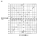
次に、主表面11内における炭化珪素基板10のエッチング量の面内分布を測定した。具体的には、島津製作所社製のフーリエ変換赤外分光光度計(型番:IRPrestige-21)を用いてエッチング量の面内分布を測定した。図6は、エッチング量を測定した炭化珪素基板10の主表面11内の位置を示している。図6において、「×」で示された位置が、エッチング量の測定位置である。具体的には、IFからCIFに向かう方向(図1における第1方向101)、OFからCOFに向かう方向(図1における第2方向102)、A-A’方向およびB-B’方向の各々に沿ってほぼ等間隔に配置された計41か所の測定位置において、エッチング量が測定された。当該41か所の測定位置におけるエッチング量の平均値および標準偏差を、それぞれ主表面11における炭化珪素基板10のエッチング量の平均値および標準偏差とした。 Next, the in-plane distribution of the etching amount of silicon carbide substrate 10 within main surface 11 was measured. Specifically, the in-plane distribution of the etching amount was measured using a Fourier transform infrared spectrophotometer (model number: IRPrestige-21) manufactured by Shimadzu Corporation. FIG. 6 shows positions within main surface 11 of silicon carbide substrate 10 where the etching amount was measured. In FIG. 6, the position indicated by "x" is the measurement position of the etching amount. Specifically, each of the direction from IF to CIF (first direction 101 in FIG. 1), direction from OF to COF (second direction 102 in FIG. 1), AA' direction and BB' direction The etching amount was measured at a total of 41 measurement positions arranged at approximately equal intervals along the . The average value and standard deviation of the etching amount at the 41 measurement positions were taken as the average value and standard deviation of the etching amount of silicon carbide substrate 10 on main surface 11, respectively.

図7は、上記4方向における炭化珪素基板10のエッチング量と測定位置との関係を示している。図7に示されるように、炭化珪素基板10のエッチング量の範囲は、0.5μm以上1.2μm以下程度であった。OFからCOFに向かう方向におけるエッチング量の標準偏差は、上記4方向の中で最も大きかった。IFからCIFに向かう方向におけるエッチング量の標準偏差は、上記4方向の中で最も小さかった。つまり、IFからCIFに向かう方向(第1方向101)におけるエッチング量の標準偏差は、OFからCOFに向かう方向(第2方向102)におけるエッチング量の標準偏差よりも小さかった。主表面11内における炭化珪素基板10のエッチング量の平均値は、1.03μmであった。主表面11内における炭化珪素基板10のエッチング量の標準偏差は、0.14μmであった。主表面11内における炭化珪素基板10のエッチング量の標準偏差を、主表面11内における炭化珪素基板10のエッチング量の平均値で除した値は、13.34%であった。つまり、主表面11内における炭化珪素基板10のエッチング量の標準偏差を、主表面11内における炭化珪素基板10のエッチング量の平均値で除した値は、15%以下であることが確かめられた。 FIG. 7 shows the relationship between the etching amount of silicon carbide substrate 10 and the measurement position in the above four directions. As shown in FIG. 7, the etching amount range of silicon carbide substrate 10 was about 0.5 μm or more and 1.2 μm or less. The standard deviation of etching amount in the direction from OF to COF was the largest among the four directions. The standard deviation of etching amount in the direction from IF to CIF was the smallest among the four directions. That is, the standard deviation of the etching amount in the direction from IF to CIF (first direction 101) was smaller than the standard deviation of the etching amount in the direction from OF to COF (second direction 102). The average etching amount of silicon carbide substrate 10 in main surface 11 was 1.03 μm. The standard deviation of the etching amount of silicon carbide substrate 10 within main surface 11 was 0.14 μm. The value obtained by dividing the standard deviation of the etching amount of silicon carbide substrate 10 within main surface 11 by the average value of the etching amount of silicon carbide substrate 10 within main surface 11 was 13.34%. That is, it was confirmed that the standard deviation of the etching amount of silicon carbide substrate 10 within main surface 11 divided by the average value of the etching amount of silicon carbide substrate 10 within main surface 11 is 15% or less. .

今回開示された実施の形態はすべての点で例示であって制限的なものではないと考えられるべきである。本発明の範囲は上記した説明ではなくて特許請求の範囲によって示され、特許請求の範囲と均等の意味および範囲内でのすべての変更が含まれることが意図される。 It should be considered that the embodiments disclosed this time are illustrative in all respects and not restrictive. The scope of the present invention is indicated by the scope of the claims rather than the above description, and is intended to include all modifications within the meaning and range of equivalents of the scope of the claims.

10 炭化珪素基板
11 主表面、第1主面
12 主表面、第2主面
13 第3主面
14 第4主面
16 第1フラット
20 炭化珪素エピタキシャル膜
100 炭化珪素エピタキシャル基板
101 第1方向
102 第2方向
111 最大径
114 厚み
200 製造装置
201 反応室
202 パイロメータ
203 発熱体
204 石英管
205 断熱材
206 誘導加熱コイル
207 ガス導入口
208 ガス排気口
209 外表面
210 サセプタ
212 回転軸
10 silicon carbide substrate 11 main surface, first main surface 12 main surface, second main surface 13 third main surface 14 fourth main surface 16 first flat 20 silicon carbide epitaxial film 100 silicon carbide epitaxial substrate 101 first direction 102 third Two directions 111 Maximum diameter 114 Thickness 200 Manufacturing device 201 Reaction chamber 202 Pyrometer 203 Heating element 204 Quartz tube 205 Heat insulating material 206 Induction heating coil 207 Gas introduction port 208 Gas exhaust port 209 Outer surface 210 Susceptor 212 Rotation shaft

Claims (4)

主表面を有する炭化珪素基板を反応室に導入する工程と、
前記反応室において、前記主表面の全面を平均値で1.5μm超10μm以下エッチングする工程と、
前記エッチングする工程後、前記反応室において、エッチングされた前記主表面上に炭化珪素エピタキシャル膜を形成する工程と、を備え、
前記主表面の全面をエッチングする工程においては、水素を含むガスが使用される、炭化珪素エピタキシャル基板の製造方法。
introducing a silicon carbide substrate having a main surface into a reaction chamber;
etching the entire surface of the main surface by an average value of more than 1.5 μm to 10 μm or less in the reaction chamber;
forming a silicon carbide epitaxial film on the etched main surface in the reaction chamber after the etching step ;
A method for manufacturing a silicon carbide epitaxial substrate , wherein a gas containing hydrogen is used in the step of etching the entire main surface .
前記主表面の全面をエッチングする工程においては、前記炭化珪素基板の温度は、1600℃以上2000℃以下である、請求項に記載の炭化珪素エピタキシャル基板の製造方法。 2. The method for manufacturing a silicon carbide epitaxial substrate according to claim 1 , wherein in the step of etching the entire main surface, the temperature of said silicon carbide substrate is 1600[deg.] C. or more and 2000[deg.] C. or less. 前記エッチングする工程において、前記主表面内における前記炭化珪素基板のエッチング量の標準偏差を、前記主表面内における前記エッチング量の前記平均値で除した値は、15%以下である、請求項1または請求項2に記載の炭化珪素エピタキシャル基板の製造方法。 2. A value obtained by dividing a standard deviation of the etching amount of said silicon carbide substrate within said main surface by said average value of said etching amount within said main surface in said etching step is 15% or less. 3. The method for manufacturing a silicon carbide epitaxial substrate according to claim 2 . 前記反応室において、前記主表面の全面が平均値で5μm以下エッチングされる、請求項1~請求項3のいずれか1項に記載の炭化珪素エピタキシャル基板の製造方法。4. The method for manufacturing a silicon carbide epitaxial substrate according to claim 1, wherein the entire surface of said main surface is etched by an average value of 5 μm or less in said reaction chamber.
JP2018111994A 2018-06-12 2018-06-12 Method for manufacturing silicon carbide epitaxial substrate Active JP7143638B2 (en)

Priority Applications (1)

Application Number Priority Date Filing Date Title
JP2018111994A JP7143638B2 (en) 2018-06-12 2018-06-12 Method for manufacturing silicon carbide epitaxial substrate

Applications Claiming Priority (1)

Application Number Priority Date Filing Date Title
JP2018111994A JP7143638B2 (en) 2018-06-12 2018-06-12 Method for manufacturing silicon carbide epitaxial substrate

Publications (2)

Publication Number Publication Date
JP2019216166A JP2019216166A (en) 2019-12-19
JP7143638B2 true JP7143638B2 (en) 2022-09-29

Family

ID=68919632

Family Applications (1)

Application Number Title Priority Date Filing Date
JP2018111994A Active JP7143638B2 (en) 2018-06-12 2018-06-12 Method for manufacturing silicon carbide epitaxial substrate

Country Status (1)

Country Link
JP (1) JP7143638B2 (en)

Families Citing this family (1)

* Cited by examiner, † Cited by third party
Publication number Priority date Publication date Assignee Title
JP2022020995A (en) 2020-07-21 2022-02-02 三菱電機株式会社 Manufacturing method of silicon carbide epitaxial wafer

Citations (2)

* Cited by examiner, † Cited by third party
Publication number Priority date Publication date Assignee Title
WO2012067112A1 (en) 2010-11-17 2012-05-24 新日本製鐵株式会社 Method for producing epitaxial silicon carbide single crystal substrate
JP2015002217A (en) 2013-06-13 2015-01-05 学校法人関西学院 Method of manufacturing sic semiconductor element

Patent Citations (2)

* Cited by examiner, † Cited by third party
Publication number Priority date Publication date Assignee Title
WO2012067112A1 (en) 2010-11-17 2012-05-24 新日本製鐵株式会社 Method for producing epitaxial silicon carbide single crystal substrate
JP2015002217A (en) 2013-06-13 2015-01-05 学校法人関西学院 Method of manufacturing sic semiconductor element

Also Published As

Publication number Publication date
JP2019216166A (en) 2019-12-19

Similar Documents

Publication Publication Date Title
JP7052851B2 (en) Method for manufacturing silicon carbide epitaxial substrate and silicon carbide semiconductor device
WO2015114961A1 (en) Silicon carbide epitaxial substrate, and method for producing silicon carbide epitaxial substrate
JP4839646B2 (en) Silicon carbide semiconductor manufacturing method and silicon carbide semiconductor manufacturing apparatus
JP2015529015A (en) SiC substrate having SiC epitaxial film
US10697086B2 (en) Method for manufacturing silicon carbide epitaxial substrate, method for manufacturing silicon carbide semiconductor device, and apparatus for manufacturing silicon carbide epitaxial substrate
JP2017109900A (en) Epitaxial growth system, epitaxial growth method, and production method of semiconductor element
WO2017090285A9 (en) Method for manufacturing silicon carbide epitaxial substrate and silicon carbide semiconductor device
JP2018108916A (en) Method for manufacturing silicon carbide epitaxial substrate
JP6915627B2 (en) Method for manufacturing silicon carbide epitaxial substrate
JP7143638B2 (en) Method for manufacturing silicon carbide epitaxial substrate
JP2018177616A (en) Method of manufacturing silicon carbide epitaxial substrate
JP2015207695A (en) Method of manufacturing epitaxial wafer and epitaxial wafer
JP6954316B2 (en) Method for manufacturing silicon carbide epitaxial substrate and silicon carbide semiconductor device
US10337119B2 (en) Method of manufacturing silicon carbide epitaxial substrate
JP2020100528A (en) Laminate, method for manufacturing laminate and method for manufacturing silicon carbide polycrystal substrate
WO2019044029A1 (en) Silicon carbide epitaxial substrate and production method for silicon carbide semiconductor device
JP7310822B2 (en) Method for manufacturing silicon carbide epitaxial substrate and method for manufacturing silicon carbide semiconductor device
WO2020039745A1 (en) Manufacturing method of silicon carbide epitaxial substrate, and manufacturing method of silicon carbide semiconductor device
JP5648442B2 (en) Silicon carbide semiconductor
JP6090552B1 (en) Method for manufacturing silicon carbide epitaxial substrate, method for manufacturing silicon carbide semiconductor device, and device for manufacturing silicon carbide epitaxial substrate
JP2014166957A5 (en)
JP5896346B2 (en) Silicon carbide semiconductor
WO2017051611A1 (en) Method for producing silicon carbide epitaxial substrate, method for manufacturing silicon carbide semiconductor device, and apparatus for producing silicon carbide epitaxial substrate
JP6747510B2 (en) Silicon carbide epitaxial substrate
JP7131146B2 (en) Method for manufacturing silicon carbide epitaxial substrate and method for manufacturing silicon carbide semiconductor device

Legal Events

Date Code Title Description
A621 Written request for application examination

Free format text: JAPANESE INTERMEDIATE CODE: A621

Effective date: 20210322

A977 Report on retrieval

Free format text: JAPANESE INTERMEDIATE CODE: A971007

Effective date: 20220127

A131 Notification of reasons for refusal

Free format text: JAPANESE INTERMEDIATE CODE: A131

Effective date: 20220201

A601 Written request for extension of time

Free format text: JAPANESE INTERMEDIATE CODE: A601

Effective date: 20220323

A521 Request for written amendment filed

Free format text: JAPANESE INTERMEDIATE CODE: A523

Effective date: 20220425

TRDD Decision of grant or rejection written
A01 Written decision to grant a patent or to grant a registration (utility model)

Free format text: JAPANESE INTERMEDIATE CODE: A01

Effective date: 20220816

A61 First payment of annual fees (during grant procedure)

Free format text: JAPANESE INTERMEDIATE CODE: A61

Effective date: 20220829

R150 Certificate of patent or registration of utility model

Ref document number: 7143638

Country of ref document: JP

Free format text: JAPANESE INTERMEDIATE CODE: R150