JP7138564B2 - photoresist composition - Google Patents
photoresist composition Download PDFInfo
- Publication number
- JP7138564B2 JP7138564B2 JP2018516193A JP2018516193A JP7138564B2 JP 7138564 B2 JP7138564 B2 JP 7138564B2 JP 2018516193 A JP2018516193 A JP 2018516193A JP 2018516193 A JP2018516193 A JP 2018516193A JP 7138564 B2 JP7138564 B2 JP 7138564B2
- Authority
- JP
- Japan
- Prior art keywords
- resist
- coating
- photoresist
- metal
- component
- Prior art date
- Legal status (The legal status is an assumption and is not a legal conclusion. Google has not performed a legal analysis and makes no representation as to the accuracy of the status listed.)
- Active
Links
Images


Classifications
-
- G—PHYSICS
- G03—PHOTOGRAPHY; CINEMATOGRAPHY; ANALOGOUS TECHNIQUES USING WAVES OTHER THAN OPTICAL WAVES; ELECTROGRAPHY; HOLOGRAPHY
- G03F—PHOTOMECHANICAL PRODUCTION OF TEXTURED OR PATTERNED SURFACES, e.g. FOR PRINTING, FOR PROCESSING OF SEMICONDUCTOR DEVICES; MATERIALS THEREFOR; ORIGINALS THEREFOR; APPARATUS SPECIALLY ADAPTED THEREFOR
- G03F7/00—Photomechanical, e.g. photolithographic, production of textured or patterned surfaces, e.g. printing surfaces; Materials therefor, e.g. comprising photoresists; Apparatus specially adapted therefor
- G03F7/004—Photosensitive materials
- G03F7/0042—Photosensitive materials with inorganic or organometallic light-sensitive compounds not otherwise provided for, e.g. inorganic resists
-
- G—PHYSICS
- G03—PHOTOGRAPHY; CINEMATOGRAPHY; ANALOGOUS TECHNIQUES USING WAVES OTHER THAN OPTICAL WAVES; ELECTROGRAPHY; HOLOGRAPHY
- G03F—PHOTOMECHANICAL PRODUCTION OF TEXTURED OR PATTERNED SURFACES, e.g. FOR PRINTING, FOR PROCESSING OF SEMICONDUCTOR DEVICES; MATERIALS THEREFOR; ORIGINALS THEREFOR; APPARATUS SPECIALLY ADAPTED THEREFOR
- G03F7/00—Photomechanical, e.g. photolithographic, production of textured or patterned surfaces, e.g. printing surfaces; Materials therefor, e.g. comprising photoresists; Apparatus specially adapted therefor
- G03F7/004—Photosensitive materials
- G03F7/027—Non-macromolecular photopolymerisable compounds having carbon-to-carbon double bonds, e.g. ethylenic compounds
- G03F7/028—Non-macromolecular photopolymerisable compounds having carbon-to-carbon double bonds, e.g. ethylenic compounds with photosensitivity-increasing substances, e.g. photoinitiators
- G03F7/031—Organic compounds not covered by group G03F7/029
-
- G—PHYSICS
- G03—PHOTOGRAPHY; CINEMATOGRAPHY; ANALOGOUS TECHNIQUES USING WAVES OTHER THAN OPTICAL WAVES; ELECTROGRAPHY; HOLOGRAPHY
- G03F—PHOTOMECHANICAL PRODUCTION OF TEXTURED OR PATTERNED SURFACES, e.g. FOR PRINTING, FOR PROCESSING OF SEMICONDUCTOR DEVICES; MATERIALS THEREFOR; ORIGINALS THEREFOR; APPARATUS SPECIALLY ADAPTED THEREFOR
- G03F7/00—Photomechanical, e.g. photolithographic, production of textured or patterned surfaces, e.g. printing surfaces; Materials therefor, e.g. comprising photoresists; Apparatus specially adapted therefor
- G03F7/004—Photosensitive materials
- G03F7/038—Macromolecular compounds which are rendered insoluble or differentially wettable
-
- G—PHYSICS
- G03—PHOTOGRAPHY; CINEMATOGRAPHY; ANALOGOUS TECHNIQUES USING WAVES OTHER THAN OPTICAL WAVES; ELECTROGRAPHY; HOLOGRAPHY
- G03F—PHOTOMECHANICAL PRODUCTION OF TEXTURED OR PATTERNED SURFACES, e.g. FOR PRINTING, FOR PROCESSING OF SEMICONDUCTOR DEVICES; MATERIALS THEREFOR; ORIGINALS THEREFOR; APPARATUS SPECIALLY ADAPTED THEREFOR
- G03F7/00—Photomechanical, e.g. photolithographic, production of textured or patterned surfaces, e.g. printing surfaces; Materials therefor, e.g. comprising photoresists; Apparatus specially adapted therefor
- G03F7/16—Coating processes; Apparatus therefor
- G03F7/162—Coating on a rotating support, e.g. using a whirler or a spinner
-
- G—PHYSICS
- G03—PHOTOGRAPHY; CINEMATOGRAPHY; ANALOGOUS TECHNIQUES USING WAVES OTHER THAN OPTICAL WAVES; ELECTROGRAPHY; HOLOGRAPHY
- G03F—PHOTOMECHANICAL PRODUCTION OF TEXTURED OR PATTERNED SURFACES, e.g. FOR PRINTING, FOR PROCESSING OF SEMICONDUCTOR DEVICES; MATERIALS THEREFOR; ORIGINALS THEREFOR; APPARATUS SPECIALLY ADAPTED THEREFOR
- G03F7/00—Photomechanical, e.g. photolithographic, production of textured or patterned surfaces, e.g. printing surfaces; Materials therefor, e.g. comprising photoresists; Apparatus specially adapted therefor
- G03F7/16—Coating processes; Apparatus therefor
- G03F7/168—Finishing the coated layer, e.g. drying, baking, soaking
-
- G—PHYSICS
- G03—PHOTOGRAPHY; CINEMATOGRAPHY; ANALOGOUS TECHNIQUES USING WAVES OTHER THAN OPTICAL WAVES; ELECTROGRAPHY; HOLOGRAPHY
- G03F—PHOTOMECHANICAL PRODUCTION OF TEXTURED OR PATTERNED SURFACES, e.g. FOR PRINTING, FOR PROCESSING OF SEMICONDUCTOR DEVICES; MATERIALS THEREFOR; ORIGINALS THEREFOR; APPARATUS SPECIALLY ADAPTED THEREFOR
- G03F7/00—Photomechanical, e.g. photolithographic, production of textured or patterned surfaces, e.g. printing surfaces; Materials therefor, e.g. comprising photoresists; Apparatus specially adapted therefor
- G03F7/20—Exposure; Apparatus therefor
- G03F7/2002—Exposure; Apparatus therefor with visible light or UV light, through an original having an opaque pattern on a transparent support, e.g. film printing, projection printing; by reflection of visible or UV light from an original such as a printed image
-
- G—PHYSICS
- G03—PHOTOGRAPHY; CINEMATOGRAPHY; ANALOGOUS TECHNIQUES USING WAVES OTHER THAN OPTICAL WAVES; ELECTROGRAPHY; HOLOGRAPHY
- G03F—PHOTOMECHANICAL PRODUCTION OF TEXTURED OR PATTERNED SURFACES, e.g. FOR PRINTING, FOR PROCESSING OF SEMICONDUCTOR DEVICES; MATERIALS THEREFOR; ORIGINALS THEREFOR; APPARATUS SPECIALLY ADAPTED THEREFOR
- G03F7/00—Photomechanical, e.g. photolithographic, production of textured or patterned surfaces, e.g. printing surfaces; Materials therefor, e.g. comprising photoresists; Apparatus specially adapted therefor
- G03F7/20—Exposure; Apparatus therefor
- G03F7/2022—Multi-step exposure, e.g. hybrid; backside exposure; blanket exposure, e.g. for image reversal; edge exposure, e.g. for edge bead removal; corrective exposure
-
- G—PHYSICS
- G03—PHOTOGRAPHY; CINEMATOGRAPHY; ANALOGOUS TECHNIQUES USING WAVES OTHER THAN OPTICAL WAVES; ELECTROGRAPHY; HOLOGRAPHY
- G03F—PHOTOMECHANICAL PRODUCTION OF TEXTURED OR PATTERNED SURFACES, e.g. FOR PRINTING, FOR PROCESSING OF SEMICONDUCTOR DEVICES; MATERIALS THEREFOR; ORIGINALS THEREFOR; APPARATUS SPECIALLY ADAPTED THEREFOR
- G03F7/00—Photomechanical, e.g. photolithographic, production of textured or patterned surfaces, e.g. printing surfaces; Materials therefor, e.g. comprising photoresists; Apparatus specially adapted therefor
- G03F7/20—Exposure; Apparatus therefor
- G03F7/2051—Exposure without an original mask, e.g. using a programmed deflection of a point source, by scanning, by drawing with a light beam, using an addressed light or corpuscular source
- G03F7/2059—Exposure without an original mask, e.g. using a programmed deflection of a point source, by scanning, by drawing with a light beam, using an addressed light or corpuscular source using a scanning corpuscular radiation beam, e.g. an electron beam
- G03F7/2061—Electron scattering (proximity) correction or prevention methods
-
- G—PHYSICS
- G03—PHOTOGRAPHY; CINEMATOGRAPHY; ANALOGOUS TECHNIQUES USING WAVES OTHER THAN OPTICAL WAVES; ELECTROGRAPHY; HOLOGRAPHY
- G03F—PHOTOMECHANICAL PRODUCTION OF TEXTURED OR PATTERNED SURFACES, e.g. FOR PRINTING, FOR PROCESSING OF SEMICONDUCTOR DEVICES; MATERIALS THEREFOR; ORIGINALS THEREFOR; APPARATUS SPECIALLY ADAPTED THEREFOR
- G03F7/00—Photomechanical, e.g. photolithographic, production of textured or patterned surfaces, e.g. printing surfaces; Materials therefor, e.g. comprising photoresists; Apparatus specially adapted therefor
- G03F7/26—Processing photosensitive materials; Apparatus therefor
- G03F7/30—Imagewise removal using liquid means
- G03F7/32—Liquid compositions therefor, e.g. developers
- G03F7/325—Non-aqueous compositions
-
- H—ELECTRICITY
- H10—SEMICONDUCTOR DEVICES; ELECTRIC SOLID-STATE DEVICES NOT OTHERWISE PROVIDED FOR
- H10P—GENERIC PROCESSES OR APPARATUS FOR THE MANUFACTURE OR TREATMENT OF DEVICES COVERED BY CLASS H10
- H10P54/00—Cutting or separating of wafers, substrates or parts of devices
-
- H—ELECTRICITY
- H10—SEMICONDUCTOR DEVICES; ELECTRIC SOLID-STATE DEVICES NOT OTHERWISE PROVIDED FOR
- H10P—GENERIC PROCESSES OR APPARATUS FOR THE MANUFACTURE OR TREATMENT OF DEVICES COVERED BY CLASS H10
- H10P76/00—Manufacture or treatment of masks on semiconductor bodies, e.g. by lithography or photolithography
- H10P76/20—Manufacture or treatment of masks on semiconductor bodies, e.g. by lithography or photolithography of masks comprising organic materials
- H10P76/204—Manufacture or treatment of masks on semiconductor bodies, e.g. by lithography or photolithography of masks comprising organic materials of organic photoresist masks
- H10P76/2041—Photolithographic processes
-
- H—ELECTRICITY
- H10—SEMICONDUCTOR DEVICES; ELECTRIC SOLID-STATE DEVICES NOT OTHERWISE PROVIDED FOR
- H10W—GENERIC PACKAGES, INTERCONNECTIONS, CONNECTORS OR OTHER CONSTRUCTIONAL DETAILS OF DEVICES COVERED BY CLASS H10
- H10W20/00—Interconnections in chips, wafers or substrates
- H10W20/01—Manufacture or treatment
- H10W20/031—Manufacture or treatment of conductive parts of the interconnections
- H10W20/0698—Local interconnections
-
- H—ELECTRICITY
- H10—SEMICONDUCTOR DEVICES; ELECTRIC SOLID-STATE DEVICES NOT OTHERWISE PROVIDED FOR
- H10W—GENERIC PACKAGES, INTERCONNECTIONS, CONNECTORS OR OTHER CONSTRUCTIONAL DETAILS OF DEVICES COVERED BY CLASS H10
- H10W74/00—Encapsulations, e.g. protective coatings
- H10W74/01—Manufacture or treatment
-
- H—ELECTRICITY
- H05—ELECTRIC TECHNIQUES NOT OTHERWISE PROVIDED FOR
- H05K—PRINTED CIRCUITS; CASINGS OR CONSTRUCTIONAL DETAILS OF ELECTRIC APPARATUS; MANUFACTURE OF ASSEMBLAGES OF ELECTRICAL COMPONENTS
- H05K3/00—Apparatus or processes for manufacturing printed circuits
- H05K3/30—Assembling printed circuits with electric components, e.g. with resistors
- H05K3/303—Assembling printed circuits with electric components, e.g. with resistors with surface mounted components
-
- H—ELECTRICITY
- H10—SEMICONDUCTOR DEVICES; ELECTRIC SOLID-STATE DEVICES NOT OTHERWISE PROVIDED FOR
- H10W—GENERIC PACKAGES, INTERCONNECTIONS, CONNECTORS OR OTHER CONSTRUCTIONAL DETAILS OF DEVICES COVERED BY CLASS H10
- H10W72/00—Interconnections or connectors in packages
- H10W72/01—Manufacture or treatment
- H10W72/019—Manufacture or treatment of bond pads
Landscapes
- Physics & Mathematics (AREA)
- General Physics & Mathematics (AREA)
- Health & Medical Sciences (AREA)
- Toxicology (AREA)
- Spectroscopy & Molecular Physics (AREA)
- Chemical & Material Sciences (AREA)
- Organic Chemistry (AREA)
- Exposure And Positioning Against Photoresist Photosensitive Materials (AREA)
- Materials For Photolithography (AREA)
- Steroid Compounds (AREA)
- Organic Low-Molecular-Weight Compounds And Preparation Thereof (AREA)
- Photosensitive Polymer And Photoresist Processing (AREA)
Description
緒言
本発明は、レジスト組成物、特にフォトレジスト組成物に関する。本発明はまた、このようなレジスト組成物の調製方法および使用方法、ならびに様々な関連態様に関する。
INTRODUCTION This invention relates to resist compositions, particularly photoresist compositions. The invention also relates to methods of preparing and using such resist compositions, and various related aspects.
当業者に周知の様々な理由のために、集積回路(IC)を小型化するためのエレクトロニクス産業における継続的な推進が存在している。半導体産業におけるめざましい発展は、ミクロンスケールからナノメートルスケールへのフォトリソグラフィの進歩により可能になったが、光学リソグラフィの物理的分解能は現在、ほぼ限界に達しているため、さらなる進歩が制約されている。しかし、半導体産業の継続的な成長は、シリコン基板上の集積回路の性能を高めることに依存している。 For various reasons well known to those skilled in the art, there is a continuing drive in the electronics industry to miniaturize integrated circuits (ICs). Tremendous progress in the semiconductor industry has been made possible by advances in photolithography from the micron scale to the nanometer scale, but further progress is constrained by the physical resolution of optical lithography, which is now near its limit. . However, the continued growth of the semiconductor industry depends on increasing the performance of integrated circuits on silicon substrates.
13.5nmでの超紫外線(EUV)リソグラフィが近年開発されたことにより、集積回路の更なるスケーリング/小型化が可能になったが、半導体産業におけるこの技術の完全な実装を依然として妨げる大きな課題がある。 Recent developments in extreme ultraviolet (EUV) lithography at 13.5 nm have enabled further scaling/miniaturization of integrated circuits, but major challenges still hamper full implementation of this technology in the semiconductor industry. be.
浸漬193nmフォトリソグラフィは、表面プラズモン共鳴および位相シフトマスクなどのサブ波長技術を利用することによってパターン形成解像能を拡張した。残念なことに、これらのレジスト材料はより長いパターニング時間を必要とし、その結果、スループットが低下する。 Immersion 193 nm photolithography has extended patterning resolution capabilities by exploiting sub-wavelength techniques such as surface plasmon resonance and phase shift masks. Unfortunately, these resist materials require longer patterning times, resulting in lower throughput.
本発明の1つの目的は、先行技術によって受け継がれた問題の少なくとも1つに対処する新規レジスト組成物を開発することである。フォトレジストはIC組み立ての分野ですでに広く使用されているので、既存の技術およびハードウェア(高価であり得る)と両立する(すなわち、後付可能である)新規レジスト組成物は、あらゆる技術移転の負担を軽減するために特に望ましい。 One object of the present invention is to develop new resist compositions that address at least one of the problems inherited by the prior art. Since photoresists are already widely used in the field of IC assembly, new resist compositions that are compatible (i.e., retrofittable) with existing technology and hardware (which can be expensive) are essential to any technology transfer. It is particularly desirable to reduce the burden on
フォトレジストは、2つの主要カテゴリー(ポジティブ型およびネガティブ型のフォトレジスト)に分類される。「ポジティブ型レジスト」(またはポジレジスト)は、レジスト現像液中で溶解性が高くなることによって暴露照射線に反応し、これにより、暴露されていない部分を乱すことなく、現像中に照射線暴露部分を除去することができる。これに対して、「ネガティブ型レジスト」(すなわち、ネガレジスト)は、レジスト現像液中で溶解性が低くなることによって暴露照射線に反応し、このため、現像中に未暴露部分が除去され、暴露部分が残る。両方の種類のレジストが有用であるが、ネガ型フォトレジストはIC組み立てにおいて特に適している。 Photoresists fall into two main categories: positive-acting and negative - acting photoresists. A "positive resist" (or positive resist) responds to exposing radiation by becoming more soluble in the resist developer, thereby allowing radiation exposure during development without disturbing the unexposed areas. parts can be removed. In contrast, "negative resists" (i.e., negative resists) respond to exposing radiation by becoming less soluble in the resist developer, thus removing unexposed portions during development, An exposed portion remains. Both types of resist are useful, but negative photoresists are particularly suitable in IC fabrication.
典型的には、既存のフォトレジストの暴露に紫外線(UV)および深紫外線(DUV)が使用されるが、波長パラメータは多くの場合、塗布されるフォトレジスト層の厚さに基づいて選択される。より薄い層は、より短い波長によって有利に暴露することができ、それにより、アスペクト比の減少およびより高い解像度を可能にする。しかし、現行のフォトレジスト技術は、解像度と暴露速度/感度(すなわち、スループット)との間の「妥協」に苦悩している。 Ultraviolet (UV) and deep ultraviolet (DUV) are typically used to expose existing photoresists, but the wavelength parameters are often selected based on the thickness of the photoresist layer to be applied. . Thinner layers can be advantageously exposed by shorter wavelengths, thereby allowing for reduced aspect ratios and higher resolution. However, current photoresist technology suffers from a "compromise" between resolution and exposure speed/sensitivity (ie, throughput).
高解像度フォトリソグラフィの鍵は、フォトレジスト暴露制御(良好な制御により、暴露されたフォトレジストが短い距離にわたって現像液と溶解性の最大コントラストを示すことができる)であり、その一方で、高速フォトリソグラフィの鍵は利用可能なエネルギーの豊富な供給である。より短いUV波長でより良好な暴露制御が得られ、より高い解像度のフォトリソグラフィパターンとなる傾向がある(より小さいスケールでフィーチャと相互作用する能力のために)が、このような短いUV波長は一般に、より短い波長で(分子および原子を吸収する)スピン許容電子遷移の広まりがより高いために、長い波長よりも(フォトレジストによって)よく吸収され、これにより、使用可能なエネルギーの供給が制限される。このような吸収事象は光子エネルギーを「引き上げる」傾向があるため、最終的な振動エネルギー散逸は通常フォトリソグラフィの観点からは無駄であり、これらの光子のエネルギーはもはやフォトリソグラフィ的に有益な方法(例えば、レジストの型に応じて、適した結合形成または結合の切断を促進することによって、フォトレジストの暴露部分と非暴露部分との溶解性を選択的に変更する化学反応を引き起こすことを介して)では利用できない。したがって、解像度の向上は、通常、フォトリソグラフィの動力学を犠牲にして行われる。 The key to high-resolution photolithography is photoresist exposure control (good control allows the exposed photoresist to exhibit maximum developer-solubility contrast over short distances), while high-speed photolithography The key to lithography is the abundant supply of available energy. Although shorter UV wavelengths tend to provide better exposure control and result in higher resolution photolithographic patterns (because of their ability to interact with features on a smaller scale), such short UV wavelengths In general, shorter wavelengths are absorbed (by photoresists) better than longer wavelengths due to the higher prevalence of spin-allowed electronic transitions (absorbing molecules and atoms), which limits the available energy supply be done. Since such absorption events tend to "raise up" the photon energy, the final vibrational energy dissipation is usually wasteful from a photolithographic point of view, and the energy of these photons is no longer photolithographically useful ( For example, by causing a chemical reaction that selectively alters the solubility of exposed and unexposed portions of the photoresist by promoting suitable bond formation or bond scission, depending on the type of resist. ) is not available. Therefore, resolution enhancements are usually made at the expense of photolithographic dynamics.
上記にかかわらず、フォトレジストをイオン化するのに十分なエネルギーを有する光子は、フォトレジスト材料の更なる暴露に次いで有益に関与し得る電子の放出(典型的には価電子帯、原子価軌道および/または最高占有分子軌道HOMOからのイオン化)を引き起こす可能性がある。本出願の文脈においては、そのような「放出」電子は二次電子と呼ばれているが、(実際には、技術とは対照的に)実際に入射一次電子はその製造に必要ではないことは理解されるであろう。このイオン化プロセスの間に光子エネルギーが吸収されるが、エネルギー(またはその少なくとも一部)は、(無駄にトラップされるというよりは)さらなる暴露事象のために有益に放出されるが、当然ながら、これは、特に、近接効果(proxomity effects)を引き起こす電子が放出される角度(約80℃)に鑑みて、暴露制御問題となり得る。 Notwithstanding the above, photons with sufficient energy to ionize the photoresist may participate beneficially subsequent to further exposure of the photoresist material to the emission of electrons (typically valence bands, valence orbitals and /or ionization from the highest occupied molecular orbital HOMO). In the context of this application, such "emitted" electrons are called secondary electrons, although in fact (in contrast to the technique) incident primary electrons are not actually required for their production. will be understood. Although photon energy is absorbed during this ionization process, the energy (or at least part of it) is beneficially released (rather than wastedly trapped) for further exposure events, but of course This can be an exposure control issue, especially in view of the angle at which the electrons are emitted (about 80° C.) which causes proximity effects.
5eV(すなわち、約248nm)の低いエネルギーを有する光子は、そのようなイオン化を誘発し得る(対応する二次電子の放出をもたらす)が、20eV(約62nm)を超える光子エネルギーは、フォトリソグラフィの観点からは一般的にあまり有益でない、より多くの内部電子イオン化およびオージェ遷移をもたらす傾向がある。したがって、有用な光子および/または対応する二次電子エネルギー範囲は5~20eVである。このような電子エネルギー(および実際には光子エネルギー)は、
-結合破壊(例えば、結合解離エネルギー:C-C(約3.60eV)、C-H(約4.5eV))、
-隣接分子/原子における別の電子イオン化事象(例えば、次いで隣接分子と反応し得るフリーラジカルなどの反応種の形成を導く)
-分子をより反応性の高い状態に置く電子励起、
などの原因によって、局在化した化学反応(電子エネルギーが一般に1つの衝突事象で完全に消費されるため「局在化」する)を引き起こすのに十分である。
Photons with energies as low as 5 eV (i.e., about 248 nm) can induce such ionization (resulting in the corresponding secondary electron emission), while photon energies above 20 eV (about 62 nm) are not suitable for photolithography. It tends to lead to more internal electron ionization and Auger transitions, which is generally less beneficial from the point of view. Therefore, the useful photon and/or corresponding secondary electron energy range is 5-20 eV. Such electronic energy (and indeed photon energy) is
- bond breaking (e.g. bond dissociation energies: C-C (about 3.60 eV), C-H (about 4.5 eV)),
- Another electron ionization event in neighboring molecules/atoms (e.g. leading to the formation of reactive species such as free radicals that can then react with neighboring molecules)
- electronic excitation that places the molecule in a more reactive state,
are sufficient to cause a localized chemical reaction (“localized” because the electron energy is generally completely consumed in one collision event) by a source such as .
ポリ(メチルメタクリレート)(PMMA)、ポリ(メチルグルタルイミド(PMGI)、フェノールホルムアルデヒド樹脂(例えばDNQ/ノボラック)、エポキシ系ポリマー(例えばSU-8)などの一般に使用されるフォトレジスト材料ポリマー材料は全て、スピンコーティングを介して基板表面(例えばシリコン)に液体として塗布することができ、表面全体にわたって均一な厚さを確保することが好ましい。 Commonly used photoresist materials such as poly(methyl methacrylate) (PMMA), poly(methyl glutarimide (PMGI), phenol formaldehyde resins (e.g. DNQ/Novolak), epoxy-based polymers (e.g. SU-8) all polymer materials , can be applied as a liquid to the substrate surface (eg silicon) via spin-coating, preferably ensuring a uniform thickness across the surface.
感度を改善することに基づいて、化学増幅化合物(例えば光酸)がフォトレジスト組成物に組み込まれることがある。暴露されると、このような化学増幅剤は、典型的に酸性化合物を放出し、その後、暴露後ベーク中に拡散され、それにより周囲/近傍のポリマーを現像剤に可溶性にする。したがって、暴露生成酸の暴露後拡散は、最終的には、現像が上手くいくために必要なフォトレジスト溶解性の差を生じさせる酸触媒反応のために重要である。非常に少量の酸でも(例えばレジストポリマーを脱保護して現像液により可溶性にするなどにより)充分な効果を引き起こす可能性があるため、現像、このため感度の向上に有益な光子衝突はほとんど必要ない。暴露/現像を確実に行うための暴露後の酸拡散(通常は暴露後のベーク中)に依存することは、特に解像度および得られるパターンのコントラストに関して、幾分制限され得る。 Based on improving sensitivity, chemical amplification compounds (eg, photoacids) are sometimes incorporated into photoresist compositions. Upon exposure , such chemical amplifiers typically release an acidic compound that then diffuses during the post- exposure bake, thereby rendering surrounding/nearby polymers soluble in the developer. Therefore, post- exposure diffusion of exposure -generated acid is important for acid-catalyzed reactions that ultimately create the difference in photoresist solubility necessary for successful development. Even very small amounts of acid can cause a sufficient effect (e.g. by deprotecting the resist polymer to make it more soluble in the developer), so that photon bombardment, which is beneficial for development and thus sensitivity improvement, is rarely necessary. do not have. Relying on post- exposure acid diffusion (usually during a post- exposure bake) to ensure exposure /development can be somewhat limiting, especially with respect to resolution and resulting pattern contrast.
したがって、本発明の目的は、従来技術の問題の少なくとも1つを解決することである。 SUMMARY OF THE INVENTION It is therefore an object of the present invention to overcome at least one of the problems of the prior art.
本発明の別の目的は、解像度と感度とのバランスが良好なレジスト組成物、好適にはフォトレジスト組成物を提供することである。 Another object of the present invention is to provide a resist composition, preferably a photoresist composition, which has a good balance between resolution and sensitivity.
本発明の第1の態様によれば、散乱防止構成成分および1つ以上のレジスト構成成分を含むレジスト組成物が提供される。好適には、散乱防止構成成分は、(一次/入射照射線および/または二次照射線のいずれかまたは両方の)散乱を低減し、それにより、良好な暴露制御をもたらし、近接効果を最小限に抑えるのにも有用である。好適には、レジスト構成成分は、組成物にレジスト特性を付与し、組成物(またはそのコーティング)の(波長/照射線に適する)照射線暴露部分の「現像液溶解性」が未暴露部分とは対照的に選択的に変換され、このため、暴露部分および未暴露部分は異なる現像剤溶解性を呈する。散乱防止構成成分およびレジスト構成成分は、別個の化合物であってもよいか、相互に会合していてもよいか、または化学的および/もしくは物理的に、好適には結合によって何らかの形で接続していてもよい。こうした会合は、それぞれの利益のために暴露制御機能と感度制御機能との間の相互作用または協働を容易にすることができ、それによって良好な感度と共に良好な解像度を生じるレジスト組成物を提供することができる。 According to a first aspect of the invention, a resist composition is provided that includes an antiscatter component and one or more resist components. Preferably, the anti-scatter component reduces scattering (of either or both primary/incident radiation and/or secondary radiation ), thereby providing good exposure control and minimizing proximity effects. It is also useful for reducing Preferably, the resist component imparts resist properties to the composition such that the "developer solubility" of the radiation - exposed portions (appropriate to the wavelength/ radiation ) of the composition (or coating thereof) is greater than that of the unexposed portions. is selectively converted, so that the exposed and unexposed areas exhibit different developer solubilities. The antiscatter component and the resist component may be separate compounds, may be associated with each other, or may be chemically and/or physically connected in some way, preferably by bonding. may be Such association can facilitate interaction or cooperation between the exposure control function and the sensitivity control function for their respective benefit, thereby providing a resist composition that produces good resolution with good sensitivity. can do.
本発明のさらなる態様によれば、散乱防止構成成分および(好適には、本明細書で定義されているような)二次電子発生剤を含むレジスト組成物が提供される。散乱防止構成成分は、好適にはレジスト構成成分であるか、またはレジスト構成成分を含む。散乱防止構成成分および二次電子発生剤は、好適には、互いに共有結合または供与結合される。 According to a further aspect of the invention there is provided a resist composition comprising an anti-scatter component and a secondary electron generator (preferably as defined herein). The anti-scatter component is preferably a resist component or comprises a resist component. The antiscatter component and secondary electron generator are preferably covalently or datively bonded to each other.
本発明のさらなる態様によれば、二次電子発生剤に共有結合によりまたは供与結合により結合された多金属ケージ化合物を含む、散乱防止-二次電子発生ハイブリッド化合物(または錯体)(AS-SEGハイブリッド)が提供される。AS-SEGハイブリッドは、多金属ケージに会合する1つ以上の配位子を介して、多金属ケージに供与結合された二次電子発生剤(好適には本明細書で定義された1つ以上の特性を有する、好適には金属中心の化合物または基)を含んでもよく、例えば、二次電子発生剤は電子対受容体(またはルイス酸)として挙動する。 According to a further aspect of the invention, an anti-scattering-secondary electron generating hybrid compound (or complex) comprising a polymetallic cage compound covalently or datively bound to a secondary electron generating agent (AS-SEG hybrid ) is provided. AS-SEG hybrids are secondary electron generators (preferably one or more (preferably metal-centered compounds or groups having the properties of ), eg, the secondary electron generator behaves as an electron pair acceptor (or Lewis acid).
本発明のさらなる態様によれば、レジストコーティング材料/基板を調製する方法が提供され、この方法は、基板をレジストコーティングでコーティングするステップを含み、レジストコーティングは、本明細書で定義される、任意的に、乾燥および/または硬化されたレジスト組成物を含む。 According to a further aspect of the invention there is provided a method of preparing a resist coating material/substrate, the method comprising coating a substrate with a resist coating , wherein the resist coating is any Generally , it includes a dried and/or cured resist composition.
本発明のさらなる態様によれば、本明細書で定義されるレジストコーティング材料/基板の調製方法によって得ることができるか、それによって得られるか、またはそれによって直接得られるレジストコーティング材料/基板が提供される。 According to a further aspect of the present invention there is provided a resist coating material/substrate obtainable by, obtained by or directly obtained by a method for preparing a resist coating material/substrate as defined herein. be done.
本発明のさらなる態様によれば、レジストコーティングでコーティングされた基板を含むレジストコーティング材料/基板が提供され、レジストコーティングは、本明細書で定義される、任意的に、乾燥および/または硬化されたレジスト組成物を含む。 According to a further aspect of the invention there is provided a resist coating material/substrate comprising a substrate coated with a resist coating, the resist coating optionally dried and /or cured as defined herein including resist compositions.
本発明のさらなる態様によれば、パターン形成された基板を調製する方法が提供され、この方法は、
i)本明細書で定義されるレジストコーティング基板を提供するステップ、または基板にレジストコーティングを塗布するステップと、
ii)レジストコーティングの一部分(複数可)を電磁波照射線に暴露させて、暴露されたレジストコーティングをもたらすステップと、
iii)暴露されたレジストコーティングを現像してレジストパターン層を生成するステップであって、レジストパターン層は、レジストコーティングの現像液不溶性コーティング部分(すなわち隆起)とレジストパターン層を通って延在する溝の列と、を含む、ステップと、を含み、
レジストコーティングは、本明細書で定義される、任意的に、乾燥および/または硬化されたレジスト組成物を含む。
According to a further aspect of the invention there is provided a method of preparing a patterned substrate, the method comprising:
i) providing a resist-coated substrate as defined herein or applying a resist coating to the substrate;
ii) exposing a portion(s) of the resist coating to electromagnetic radiation to provide an exposed resist coating;
iii) developing the exposed resist coating to produce a patterned resist layer, the patterned resist layer comprising developer-insoluble coating portions (i.e., ridges) of the resist coating and grooves extending through the patterned resist layer; including steps of
A resist coating comprises an optionally dried and /or cured resist composition as defined herein.
本発明のさらなる態様によれば、本明細書で定義されるパターン形成された基板を調製する方法によって得ることができる、得られる、または直接得られるパターン形成された基板が提供される。 According to a further aspect of the invention there is provided a patterned substrate obtainable, obtained or directly obtained by the method of preparing a patterned substrate defined herein.
本発明のさらなる態様によれば、イメージング方法が提供され、この方法は、
i)本明細書で定義されるレジストコーティング基板を提供するステップ、または基板にレジストコーティングを塗布するステップと、
ii)レジストコーティングの一部分(複数可)を電磁波照射線に暴露させて、暴露されたレジストコーティングをもたらすステップと、
iii)暴露されたレジストコーティングを現像してレジストパターン層を生成するステップであって、レジストパターン層は、レジストコーティングの現像液不溶性コーティング部分(すなわち隆起)とレジストパターン層を通って延在する溝の列と、を含む、ステップと、を含み、
レジストコーティングは、本明細書で定義される、任意的に、乾燥および/または硬化されたレジスト組成物を含む。
According to a further aspect of the invention there is provided an imaging method, the method comprising:
i) providing a resist-coated substrate as defined herein or applying a resist coating to the substrate;
ii) exposing a portion(s) of the resist coating to electromagnetic radiation to provide an exposed resist coating;
iii) developing the exposed resist coating to produce a patterned resist layer, the patterned resist layer comprising developer-insoluble coating portions (i.e., ridges) of the resist coating and grooves extending through the patterned resist layer; including steps of
A resist coating comprises an optionally dried and /or cured resist composition as defined herein.
本発明のさらなる態様によれば、リソグラフィを実施する方法が提供され、この方法は、
i)本明細書で定義されるレジストコーティング基板を提供するステップ、または基板にレジストコーティングを塗布するステップと、
ii)レジストコーティングの一部分(複数可)を照射線に暴露させて、暴露されたレジストコーティングをもたらすステップと、
iii)上記暴露されたレジストコーティングを現像してレジストパターン層を生成するステップであって、上記レジストパターン層は、上記レジストコーティングの現像液不溶性コーティング部分(すなわち隆起)と上記レジストパターン層を通って延在する溝の列と、を含む、ステップと、
iv)上記レジストパターン層の下にある上記基板、基板表面またはその一部分(複数可)を改変する任意的ステップと、
v)上記レジストパターン層を除去して改変された基板を提供する任意的ステップと、
vi)上記改変された基板において、ステップiv)および/またはステップi)~v)を任意的に1回以上繰り返すこと(任意により、上記レジストコーティングの代わりに標準的なフォトレジストなどの代替的レジストコーティングを用いて、および任意により暴露中に代替照射線を使用すること)と、を含み、
この方法のステップ(i)より前に、レジストコーティングまたは代替的レジストコーティングのいずれかを用いて、および暴露中に電磁波照射線または代替照射線のいずれかを用いて、ステップ(i)~(vi)(すなわち、前工程(i)~(vi))を実施することが、任意により1回以上繰り返され、
上記レジストコーティングは、本明細書で定義される、任意的に、乾燥および/または硬化されたレジスト組成物を含む。
According to a further aspect of the invention there is provided a method of performing lithography, the method comprising:
i) providing a resist-coated substrate as defined herein or applying a resist coating to the substrate;
ii) exposing a portion(s) of the resist coating to radiation resulting in an exposed resist coating;
iii) developing said exposed resist coating to produce a patterned resist layer, said patterned resist layer passing through developer insoluble coating portions (i.e. ridges) of said resist coating and said patterned resist layer; a step including an extending row of grooves;
iv) optionally modifying the substrate, substrate surface or portion(s) thereof underlying the resist pattern layer;
v) an optional step of removing the resist pattern layer to provide a modified substrate;
vi) optionally repeating step iv) and/or steps i)-v) one or more times on said modified substrate (optionally replacing said resist coating with an alternative resist such as standard photoresist); with the coating and optionally using alternative radiation during exposure );
Prior to step (i) of the method, with either a resist coating or an alternative resist coating, and with either electromagnetic radiation or alternative radiation during exposure , steps (i)-( vi) (i.e., performing the preceding steps (i)-(vi)) is optionally repeated one or more times,
The resist coating comprises an optionally dried and/or cured resist composition as defined herein.
本発明のさらなる態様によれば、本明細書で定義されるリソグラフィを実施する方法によって得ることができるか、得られるか、または直接得られるイメージング形成された基板が提供される。 According to a further aspect of the invention there is provided an imaged substrate obtainable, obtained or obtained directly by a method of performing lithography as defined herein.
本発明のさらなる態様によれば、リソグラフィマスク(例えば、フォトマスク)を製造する方法が提供され、この方法は、
i)本明細書で定義されるレジストコーティング基板を提供するステップ、または基板(好適にはリソグラフィにおける使用に適した基板)にレジストコーティングを塗布するステップと、
ii)レジストコーティングの一部分(複数可)を電磁波照射線に暴露させて、暴露されたレジストコーティングをもたらすステップと、
iii)上記暴露されたレジストコーティングを現像してレジストパターン層を生成するステップであって、上記レジストパターン層は、上記レジストコーティングの現像液不溶性コーティング部分(すなわち隆起)と上記レジストパターン層を通って延在する溝の列と、を含む、ステップと、
iv)(好適には、基板または基板表面の改変された部分(複数可)が所定のタイプの照射線(例えば、元の基板または基板または基板表面の未改変の部分(複数可)に対するフォトリソグラフィで使用される照射線)に対して透明度が増加または減少するように)上記レジストパターン層の下にある上記基板、基板表面またはその一部分(複数可)を選択的に改変する任意的ステップと、
v)上記レジストパターン層を除去して改変された基板を提供する任意的ステップと、を含み、
上記レジストコーティングは、本明細書で定義される、任意的に、乾燥および/または硬化されたレジスト組成物を含む。
According to a further aspect of the invention, there is provided a method of manufacturing a lithographic mask (e.g., photomask), comprising:
i) providing a resist-coated substrate as defined herein or applying a resist coating to a substrate, preferably a substrate suitable for use in lithography;
ii) exposing a portion(s) of the resist coating to electromagnetic radiation to provide an exposed resist coating;
iii) developing said exposed resist coating to produce a patterned resist layer, said patterned resist layer passing through developer insoluble coating portions (i.e. ridges) of said resist coating and said patterned resist layer; a step including an extending row of grooves;
iv) (preferably the substrate or the modified portion(s) of the substrate surface is photolithographically directed against a predetermined type of radiation (e.g. the original substrate or the unmodified portion(s) of the substrate or substrate surface); selectively modifying the substrate, substrate surface or portion(s) thereof underlying the patterned resist layer so as to increase or decrease its transparency to the radiation used in
v) optionally removing the resist pattern layer to provide a modified substrate;
The resist coating comprises an optionally dried and/or cured resist composition as defined herein.
本発明のさらなる態様によれば、本明細書で定義されるリソグラフィマスク(例えば、フォトマスク)の製造方法によって得ることができるか、得られるか、または直接得られるリソグラフィマスク(例えば、フォトマスク)が提供される。 According to a further aspect of the present invention, a lithographic mask (e.g. photomask) obtainable, obtained or directly obtainable by a method for manufacturing a lithographic mask (e.g. photomask) as defined herein is provided.
本発明のさらなる態様によれば、リソグラフィを実施する方法が提供され、この方法は、
i)レジストコーティングされた基板を提供するステップ、または基板にレジストコーティングを塗布するステップ(レジストコーティングは、リソグラフィマスク、例えばフォトレジストを介して暴露するのに適した任意のレジストコーティングであり得る)と、
ii)暴露されたレジストコーティングをもたらすために、本明細書で定義されるリソグラフィマスク(例えば、フォトマスク)を通って(または本明細書で定義される方法によって得ることができる)レジストコーティングの一部分(複数可)を照射線(例えばUVまたは可視光線)に暴露させるステップと、
iii)上記暴露されたレジストコーティングを現像してレジストパターン層を生成するステップであって、上記レジストパターン層は、上記レジストコーティングの現像液不溶性コーティング部分(すなわち隆起)と上記レジストパターン層を通って延在する溝の列と、を含む、ステップと、
iv)上記レジストパターン層の下にある上記基板、基板表面またはその一部分(複数可)を改変する任意的ステップと、
v)上記レジストパターン層を除去して改変された基板を提供する任意的ステップと、
vi)上記改変された基板において、(本発明のレジストコーティングまたは標準的なフォトレジストなどの代替的レジストコーティングのいずれかを用いて、および暴露中にリソグラフィマスクまたは代替照射線の有無にかかわらず任意により電磁波照射線を使用して)ステップiv)および/またはステップi)~v)を任意的に1回以上繰り返すことと、を含み、
この方法のステップ(i)より前に、レジストコーティングまたは代替的レジストコーティングのいずれかを用いて、および暴露中に電磁波照射線または代替照射線のいずれかを用いて、この方法のステップ(i)~(vi)(すなわち、前工程(i)~(vi))を実施することがおよび/またはフォトリソグラフィの実施方法が、任意により1回以上繰り返される。
According to a further aspect of the invention there is provided a method of performing lithography, the method comprising:
i) providing a resist-coated substrate or applying a resist coating to the substrate (the resist coating can be any resist coating suitable for exposure through a lithographic mask, e.g. photoresist); ,
ii) a portion of the resist coating through a lithographic mask (e.g., photomask) as defined herein (or obtainable by a method as defined herein) to provide an exposed resist coating; exposing the(s) to radiation (e.g. UV or visible light);
iii) developing said exposed resist coating to produce a patterned resist layer, said patterned resist layer passing through developer insoluble coating portions (i.e. ridges) of said resist coating and said patterned resist layer; a step including an extending row of grooves;
iv) optionally modifying the substrate, substrate surface or portion(s) thereof underlying the resist pattern layer;
v) an optional step of removing the resist pattern layer to provide a modified substrate;
vi) in the above modified substrates (using either the resist coating of the invention or an alternative resist coating such as a standard photoresist, and with or without a lithographic mask or alternative radiation during exposure ; optionally optionally repeating steps iv) and/or steps i)-v) one or more times using electromagnetic radiation by
Prior to step (i) of the method, with either a resist coating or an alternative resist coating and during exposure with either electromagnetic radiation or an alternative radiation , step (i) of the method )-(vi) (ie, pre-steps (i)-(vi)) and/or the photolithography method is optionally repeated one or more times.
本発明のさらなる態様によれば、本明細書で定義されるリソグラフィを実施する方法によって得ることができるか、得られるか、または直接得られるイメージング形成された基板が提供される。 According to a further aspect of the invention there is provided an imaged substrate obtainable, obtained or obtained directly by a method of performing lithography as defined herein.
本発明のさらなる態様によれば、集積回路ダイ、または複数の集積回路ダイを含む集積回路ウェハを作る方法が提供され、上記集積回路ダイまたは上記複数の集積回路ダイの各ダイは複数の電子部品を含み、この方法は、
i)本明細書で定義されるレジストコーティング基板を提供するステップ、または基板にレジストコーティングを塗布するステップと、
ii)上記レジストコーティングの一部分(複数可)を照射線(例えば、UV)に暴露させて、暴露されたレジストコーティングをもたらすステップと、
または
i)レジストコーティングされた基板を提供するステップ、または基板にレジストコーティングを塗布するステップ(レジストコーティングは、リソグラフィマスク、例えばフォトレジストを介して暴露するのに適した任意のレジストコーティングであり得る)と、
ii)暴露されたレジストコーティングをもたらすために、本明細書で定義されるリソグラフィマスク(例えば、フォトマスク)を通って(または本明細書で定義される方法によって得ることができる)レジストコーティングの一部分(複数可)を照射線(例えばUVまたは可視光線)に暴露させるステップと、
および
iii)上記暴露されたレジストコーティングを現像してレジストパターン層を生成するステップであって、上記レジストパターン層は、上記レジストコーティングの現像液不溶性コーティング部分(すなわち隆起)と上記レジストパターン層を通って延在する溝の列と、を含む、ステップと、
iv)上記レジストパターン層の下にある上記基板、基板表面またはその一部分(複数可)を改変するステップ(これには、上記ダイまたは上記各ダイの電子部品を導体(複数可)に導電的に相互接続することを伴い得る)と、
v)上記レジストパターン層を除去して改変された基板を提供するステップと、
vi)上記改変された基板上で、ステップiv)および/またはステップi)~v)を任意的に1回以上繰り返すことと(本発明のレジストコーティングまたは代替的レジストコーティングのいずれかを用いて、かつ暴露中に代替照射線を任意により使用すること)と、
vii)外部接触端子を集積回路に提供するために、(1つ以上の基板/基板表面改変ステップ中にまだ実施されていない場合)、上記ダイまたは上記各ダイの上記電子部品を導体(複数可)に任意により導電的に相互接続するステップと、
viii)任意により1つ以上の更なる仕上げステップを実施するステップと、
ix)集積回路ダイを複数の集積回路ダイを含むウェハから任意により分離させるステップと、を含み、
この方法のステップ(i)より前に、本発明のレジストコーティングまたは代替的レジストコーティングのいずれかを使用して、この方法のステップ(i)~(vi)(すなわち前ステップ(i)~(vi)、任意により2つのステップ(i)/(ii)の組み合わせのいずれかを用いて)を実施すること、および/または、リソグラフィを実施する上記方法のステップ(i)~(vi)を実施することを任意により先に行い、任意により、1回以上繰り返すステップと、を含み、
上記レジストコーティングは、本明細書で定義される、任意的に、乾燥および/または硬化されたレジスト組成物を含む。
According to a further aspect of the invention, there is provided a method of making an integrated circuit die or an integrated circuit wafer comprising a plurality of integrated circuit dies, each die of said integrated circuit die or said plurality of integrated circuit dies comprising a plurality of electronic components. and the method includes
i) providing a resist-coated substrate as defined herein or applying a resist coating to the substrate;
ii) exposing a portion(s) of the resist coating to radiation (e.g., UV) to provide an exposed resist coating;
or i) providing a resist-coated substrate or applying a resist coating to the substrate (the resist coating can be any resist coating suitable for exposure through a lithographic mask, e.g. photoresist); When,
ii) a portion of the resist coating through a lithographic mask (e.g., photomask) as defined herein (or obtainable by a method as defined herein) to provide an exposed resist coating; exposing the(s) to radiation (e.g. UV or visible light);
and iii) developing said exposed resist coating to produce a patterned resist layer, said patterned resist layer passing through developer insoluble coating portions (i.e. ridges) of said resist coating and said patterned resist layer. a row of grooves extending through a step;
iv) modifying the substrate, substrate surface, or portion(s) thereof underlying the resist pattern layer, including rendering the die or electronic components of each die electrically conductive to conductor(s); interconnecting) and
v) removing the resist pattern layer to provide a modified substrate;
vi) optionally repeating steps iv) and/or steps i)-v) one or more times on the modified substrate (using either the resist coating of the present invention or an alternative resist coating, and optional use of alternative radiation during exposure );
vii) conductor(s) of said electronic components of said die or each said die (if not already performed during one or more substrate/substrate surface modification steps) to provide external contact terminals to an integrated circuit; ), optionally conductively interconnecting the
viii) optionally performing one or more further finishing steps;
ix) optionally separating an integrated circuit die from a wafer containing a plurality of integrated circuit dies;
Prior to step (i) of the method, using either the resist coating of the present invention or an alternative resist coating, steps (i)-(vi) of the method (i.e., pre-steps (i)-(vi) ), optionally using any combination of the two steps (i)/(ii)), and/or performing steps (i)-(vi) of the above method of performing lithography optionally preceding and optionally repeating one or more times of
The resist coating comprises an optionally dried and/or cured resist composition as defined herein.
本発明のさらなる態様によれば、本明細書で定義される集積回路ダイを作る上記方法によって得られることができるか、それによって得られたか、またはそれによって直接得られた集積回路ダイが提供される。 According to a further aspect of the invention there is provided an integrated circuit die obtainable by, obtained by or directly obtained by the above method of making an integrated circuit die as defined herein. be.
本発明のさらなる態様によれば、複数の集積回路ダイを含む集積回路ウェハが提供され、集積回路ウェハは、本明細書で定義される集積回路ウェハを作る方法によって得ることができるか、それによって得られたか、またはそれによって直接得られる。このような集積回路およびウェハは、非常に高い抵抗性、高いドライエッチング選択性(典型的には20:1を超える、すなわち、レジストが下地のシリコン基板より20倍以上遅くエッチングされる)を有する。これにより、高いアスペクト比が得られる。 According to a further aspect of the invention there is provided an integrated circuit wafer comprising a plurality of integrated circuit dies, the integrated circuit wafer being obtainable by or by a method of making an integrated circuit wafer as defined herein. Obtained by or directly obtained by. Such integrated circuits and wafers have very high resistivity, high dry etch selectivity (typically greater than 20:1, i.e. the resist etches more than 20 times slower than the underlying silicon substrate). . This provides a high aspect ratio.
本発明の他の態様によれば、集積回路パッケージを製造する方法が提供され、上記集積回路パッケージは、複数のピンおよび対応する複数のピンに導電的に接続された外部接触端子を有する集積回路ダイを備え、この方法は、
i)本明細書で定義される集積回路ダイを提供するステップ、または本明細書で定義される集積回路ダイを作る方法によって集積回路ダイを作るステップと、
ii)上記集積回路ダイをパッケージ基板に取り付けるステップであって、上記パッケージ基板は電気接点を含み、上記電気接点の各々は、対応するピンに任意により、接続されるかまたは接続可能である、ステップと、
iii)上記集積回路ダイの上記外部接触端子の各々を上記パッケージ基板の対応する電気接点に導電的に接続するステップと、
iv)上記パッケージ基板の上記電気接点を対応するピンに任意により(必要に応じて)接続するステップと、
v)上記集積回路ダイをカプセル封入するステップと、を含む。
According to another aspect of the invention, a method is provided for manufacturing an integrated circuit package, the integrated circuit package having a plurality of pins and external contact terminals conductively connected to a corresponding plurality of pins. comprising a die, the method comprising:
i) providing an integrated circuit die as defined herein or making an integrated circuit die by a method of making an integrated circuit die as defined herein;
ii) attaching the integrated circuit die to a package substrate, the package substrate including electrical contacts, each of the electrical contacts optionally connected or connectable to a corresponding pin; When,
iii) conductively connecting each of said external contact terminals of said integrated circuit die to a corresponding electrical contact of said package substrate;
iv) optionally (as needed) connecting the electrical contacts of the package substrate to corresponding pins;
v) encapsulating said integrated circuit die.
本発明のさらなる態様によれば、本明細書で定義される集積回路パッケージの製造方法によって得られることができ、得られ、または直接得られる集積回路パッケージが提供される。 According to a further aspect of the present invention there is provided an integrated circuit package obtainable, obtained or directly obtainable by the integrated circuit package manufacturing method defined herein.
本発明のさらなる態様によれば、複数のピンを含む集積回路パッケージ(好適には、本明細書では定義されている)を含む回路基板を製造する方法が提供され、この方法は、
i)本明細書で定義される集積回路パッケージを提供するステップ、または本明細書で定義される集積回路パッケージを製造する方法によって集積回路パッケージを製造するステップと、
ii)集積回路パッケージを回路基板に導電的に接続するステップと、を含む。
According to a further aspect of the invention there is provided a method of manufacturing a circuit board comprising an integrated circuit package (preferably defined herein) comprising a plurality of pins, the method comprising:
i) providing an integrated circuit package as defined herein or manufacturing an integrated circuit package by a method for manufacturing an integrated circuit package as defined herein;
ii) conductively connecting the integrated circuit package to the circuit board.
本発明のさらなる態様によれば、本明細書で定義される回路基板の製造方法によって得られることができ、得られ、または直接得られる回路基板が提供される。 According to a further aspect of the invention there is provided a circuit board obtainable, obtained or directly obtainable by the method of manufacturing a circuit board as defined herein.
本発明のさらなる態様によれば、電子デバイスまたはシステムを製造する方法が提供され、電子デバイスまたはシステムは、電源を含むか、電源に接続可能であり、また、電源に導電的に接続されるか、または電源に接続可能である回路基板を含み、この方法は、
i)本明細書で定義される回路基板を提供するステップ、または本明細書で定義される回路基板を製造する方法によって回路基板を製造するステップと、
ii)電子デバイスまたはシステム内に回路基板を組み込むステップと、を含む。
According to a further aspect of the invention, there is provided a method of manufacturing an electronic device or system, wherein the electronic device or system includes, is connectable to, and is conductively connected to a power source. , or a circuit board connectable to a power supply, the method comprising:
i) providing a circuit board as defined herein or manufacturing a circuit board by a method for manufacturing a circuit board as defined herein;
ii) incorporating the circuit board into an electronic device or system.
本発明のさらなる態様によれば、本明細書で定義される電子デバイスまたはシステムの製造方法によって得られることができ、得られ、または直接得られる電子デバイスまたはシステムが提供される。 According to a further aspect of the invention there is provided an electronic device or system obtainable, obtained or directly obtainable by the method of manufacturing an electronic device or system defined herein.
本発明のさらなる態様によれば、レジストコーティングで基板をコーティングするため、基板をパターニングするため、イメージングするため、リソグラフィにおけるレジストコーティングとして、基板の表面を選択的に改変するため、リソグラフィマスク(リソグラフィの実施または集積回路の製造に使用されるマスクなど)を製造するため、多層基板を製造するため、集積回路ダイを作るため、集積回路ウェハを作るため、集積回路パッケージを製造するため、回路基板を製造するため、または電子デバイスまたはシステムを製造するため、のレジスト組成物の使用が提供される。 According to a further aspect of the present invention, for coating a substrate with a resist coating, for patterning a substrate, for imaging, as a resist coating in lithography, for selectively modifying the surface of a substrate, a lithography mask (lithography). masks used in the fabrication of integrated circuits); to fabricate multi-layer substrates; to make integrated circuit dies; to make integrated circuit wafers; Use of the resist composition for manufacturing or for manufacturing electronic devices or systems is provided.
本発明のレジスト組成物は、UV、eBeamなどの各種の照射線源と共に好適に用いることができるが、最も好適には、レジスト組成物は、フォトリソグラフィにおいて使用するためのフォトレジスト組成物であり、好適にも、いずれのレジスト構成成分もフォトレジスト構成成分である。 Although the resist compositions of the invention can be suitably used with various radiation sources such as UV, eBeam, etc., most preferably the resist compositions are photoresist compositions for use in photolithography. Preferably, any resist component is a photoresist component.
しかし、本発明はまた、「組成物」など、本発明のさらなる態様を提供し、組成物は、例えば、本明細書で定義されるあらゆるレジスト組成物の成分、特性、またはパラメータのいずれかを適切に定義または適切に継承する。このような「組成物」は、レジストまたはリソグラフィ技術以外の用途に利用することができる。例えば、組成物は、自己治癒組成物として、例えば、単独でもしくは自己治癒を必要とする1つ以上のポリマーを混合して、配置することができる。次いで、自己治癒は、本明細書で定義される電磁波照射線によって誘導され得る。 However, the invention also provides further aspects of the invention, such as "compositions," which, for example, contain any of the components, properties, or parameters of any resist composition defined herein. Well defined or properly inherited. Such "compositions" can be used in applications other than resists or lithographic techniques. For example, the composition can be deployed as a self-healing composition, eg, alone or mixed with one or more polymers requiring self-healing. Self-healing can then be induced by electromagnetic radiation as defined herein.
本発明のさらなる態様において、本明細書で定義される散乱防止構成成分または化合物が提供される。 In a further aspect of the invention there is provided an anti-scattering component or compound as defined herein.
本発明のさらなる態様において、本明細書に定義される散乱防止-レジストハイブリッド構成成分または化合物が提供される。 In a further aspect of the invention there is provided an anti-scatter-resist hybrid component or compound as defined herein.
本発明の任意の特定の態様に関連して説明される、任意の、好適な、および好ましい特徴などのいかなる特徴も、本発明のあらゆる他の態様の任意の、好適なかつ好ましい特徴などの特徴であってもよい。 Any feature, such as any preferred and preferred feature, described in relation to any particular aspect of the invention may be any feature, such as any preferred and preferred feature, of any other aspect of the invention. There may be.
本発明をより良く理解し、同じものの実施形態がどのように実施されるかを示すために、一例として以下の概略図を参照する。 For a better understanding of the invention and to show how embodiments of the same may be implemented, reference is made, by way of example, to the following schematic drawings.
定義
特に明記しない限り、本明細書および特許請求の範囲で使用される以下の用語は、以下に示す以下の意味を有する。
Definitions Unless otherwise stated, the following terms used in the specification and claims have the following meanings given below.
本明細書では、別段の記載がない限り、用語「照射線(radiation)」および「照射(irradiation)」は、レジスト組成物、またはそのコーティングを、レジスト組成物において物理的または化学的変化を引き起こし、これにより、「配置される」照射線に暴露されることを意味する。問題になっている照射線は、任意の好適な照射線であってもよい。電子ビームリソグラフィが実施される場合、その照射線は電子ビーム照射線であり、フォトリソグラフィが実施される場合、電磁波照射線(通常はUV)が使用される。 As used herein, unless otherwise stated, the terms " radiation " and "irradiation" refer to the resist composition, or coating thereof, causing physical or chemical changes in the resist composition. , by which is meant to be exposed to "placed" radiation . The radiation in question may be any suitable radiation . When e-beam lithography is performed, the radiation is e-beam radiation , and when photolithography is performed, electromagnetic radiation (usually UV) is used.
「レジスト構成成分」は、関連する照射線(例えば、電子ビーム照射線、電離照射線、紫外線)に暴露されると変化を受ける構成成分である。いくつかの実施形態では、散乱防止構成成分は、特に、それが暴露下で(またはその直後に)反応して、異なる溶解性の構成成分を生じる場合、レジスト構成成分である。しかし、好適には、レジスト構成成分は、それ自体が散乱防止構成成分ではないが、いくつかの実施形態では、散乱防止構成成分の一部分であってもよい(または散乱防止構成成分に会合していてもよい)。例えば、散乱防止構成成分は、一緒になって単一の化合物または構成成分を形成するように、レジスト構成成分(または実際には多重のレジスト構成成分がそれぞれの場合、同じまたは異なる)に結合されてもよく、これらは、レジスト/散乱防止ハイブリッドとも称され得る。いくつかの実施形態では、1つ以上の追加のレジスト構成成分(複数可)は、レジスト組成物内に、例えばPMMAなどの標準レジストポリマー内に含めることができる。本発明の範囲から除外されたレジスト組成物が使用される場合、このような組成物は、ポリマー構成成分などの他のレジスト構成成分を含んでいてもよく、任意により(実質的に)散乱防止化合物を含まなくてもよい。 A "resist component" is a component that undergoes change upon exposure to relevant radiation (eg, electron beam radiation , ionizing radiation , ultraviolet radiation). In some embodiments, the anti-scatter component is a resist component, especially if it reacts under (or shortly thereafter) exposure to yield different soluble components. Preferably, however, the resist component is not itself an anti-scatter component, but in some embodiments may be part of (or associated with) an anti-scatter component. may be used). For example, the anti-scatter component is combined with a resist component (or indeed multiple resist components in each case, the same or different) so that together they form a single compound or component. and they may also be referred to as resist/anti-scatter hybrids. In some embodiments, one or more additional resist component(s) can be included within the resist composition, for example within a standard resist polymer such as PMMA. Where resist compositions excluded from the scope of the present invention are used, such compositions may contain other resist components such as polymeric components and optionally (substantially) anti-scatter It may contain no compound.
本明細書では、「レジスト組成物」、「レジストコーティング」、「レジスト材料」、および「レジストコーティング材料」などの非限定的な言及は、本発明のレジスト組成物、コーティング、材料、またはコーティング材料に関連してもよいか、または代替的レジスト組成物、コーティング、材料、またはコーティング材料に関連してもよい。最も好ましくは、レジスト組成物、コーティング、材料、またはコーティング材料に対する非限定的な言及は、代替的レジストを指す。 As used herein, non-limiting references such as "resist composition," "resist coating," "resist material," and "resist coating material" refer to the resist composition, coating, material, or coating material of the present invention. or to alternative resist compositions, coatings, materials, or coating materials. Most preferably, non-limiting references to resist compositions, coatings, materials, or coating materials refer to alternative resists.
「代替的レジスト組成物」およびコーティングは、当業者に周知の標準的な工房技術に従って製造して使用することができる。これらは、本発明のレジスト組成物およびコーティング(コーティング、暴露、現像、除去などの方法を含む)に関して本明細書で定義したのと同じ様式で使用することもできるが、当業者であれば、本明細書で定義した方法を問題になっている代替的レジストに適するように容易に適合させ得る。 "Alternative resist compositions" and coatings can be manufactured and used according to standard laboratory techniques well known to those skilled in the art. Although they can also be used in the same manner as defined herein for the resist compositions and coatings of the invention (including methods of coating, exposing , developing, removing, etc.), those skilled in the art will The methods defined herein can be readily adapted to suit the alternative resists in question.
本明細書では、レジスト組成物内の(それ自体がレジスト構成成分であるか、そうでなければレジスト構成成分と会合するか、またはレジスト構成成分に結合されることがある)「散乱防止化合物」は、レジストパターニング時の入射照射線、散乱照射線および/または二次電子の衝撃を調節かつ制御するのに役立つ。散乱事象を最小限に抑えることにより、散乱防止化合物は、こうした照射線を所望の暴露部位に集中させて指向させることを補助し、それによって望ましくない暴露を最小限にすると考えられる。これにより、問題になっているレジスト内でより鮮明で高解像度の画像をパターン形成することが可能になる。さらに、散乱防止化合物は、レジスト内の特定の脆弱な構成成分の過剰暴露を防止または低減する可能性があり、これにより別の方法で暴露されたレジストのその後の現像を損なう可能性がある。したがって、散乱防止化合物は、ぶれを低減すること、近接効果(すなわち、別の方法でレジストの未暴露部分へのエネルギーのこぼれ)を低減すること、解像度を上げること、およびアスペクト比を増加させることが可能である(アスペクト比とは、深さを溝や隆起部などの関連するパターン線の幅で割ったものである)。(中性化合物とするにあたって)その電荷が取り消すことはない1つ以上の錯体を散乱防止化合物が含有すると記載されている場合、実際の散乱防止化合物は、非中性の錯体の組み合わせの好適な塩である(従って、全体として中性化合物となる)。当業者であれば、残りの電荷はいずれも一般的に適している対カチオンまたは対アニオンによって中和されることを十分に理解するであろう。このように、全本明細書において、散乱防止化合物および実際にはいずれの錯体も、対イオンなく定義することができる。 As used herein, an "anti-scattering compound" (which itself may be a resist component, otherwise associated with, or bound to a resist component) within the resist composition helps regulate and control the impact of incident radiation , scattered radiation and/or secondary electrons during resist patterning. By minimizing scattering events, anti-scattering compounds are believed to help focus and direct such radiation to the desired exposure site, thereby minimizing unwanted exposure . This allows for sharper, higher resolution images to be patterned in the resist in question. Additionally, anti-scatter compounds can prevent or reduce overexposure of certain vulnerable components in the resist, which can impair subsequent development of otherwise exposed resist. Therefore, anti-scatter compounds are useful for reducing blur, reducing proximity effect (i.e., energy spillover to otherwise unexposed portions of resist), increasing resolution, and increasing aspect ratio. (the aspect ratio is the depth divided by the width of the relevant pattern lines, such as grooves and ridges). When an anti-scattering compound is described as containing one or more complexes whose charges are not canceled (in terms of neutral compounds), the actual anti-scattering compound is a combination of non-neutral complexes. It is a salt (and therefore an overall neutral compound). Those skilled in the art will appreciate that any remaining charge is generally neutralized by a suitable countercation or counteranion. Thus, throughout this specification, anti-scattering compounds and indeed any complex can be defined without a counterion.
本明細書において、用語「現像液不溶性」は、所与のコーティング部分が、対応する「現像液可溶性」コーティング部分よりも比較的低い溶解性を現像液において有することを表すことを意図するものとする。現像液中の「現像液不溶性」のコーティング部分が部分的またはさらに完全な溶解性を有する(現像時間が十分に長い場合)ことを必ずしも排除するものではない。当業者には理解されるように、コーティング部分は、「現像液可溶性」および「現像液不溶性」として示差的に指定され、コーティングの部分(例えば、照射線に暴露された部分)がコーティングの他の部分(例えば、照射線に暴露されていない部分)に対して異なる溶解特性、したがって、典型的には異なる化学的性質を有することを示す。現像液の性質は、それぞれのコーティング部分の異なる溶解度特性に基づき、コーティングのどの部分を除去することを意図しているかに応じて慎重に選択することができるため、重要ではない。一般に、現像の文脈で使用される用語「溶解性」は、当業者に理解されるように、熱力学的溶解性が動力学的溶解性と相関し得るが、可溶化の速度が重要であるため、熱力学的溶解性よりも動力学的溶解性に関する。 As used herein, the term "developer-insoluble" is intended to indicate that a given coating portion has relatively lower solubility in a developer than a corresponding "developer-soluble" coating portion. do. It does not necessarily exclude that portions of the coating that are "developer-insoluble" in the developer have partial or even complete solubility (if the development time is long enough). As will be appreciated by those skilled in the art, portions of the coating are designated differentially as "developer soluble" and "developer insoluble," indicating that portions of the coating (e.g., portions exposed to radiation ) are have different dissolution properties, and therefore typically different chemical properties, for portions of (eg, those not exposed to radiation ). The nature of the developer is not critical as it can be carefully selected depending on which parts of the coating are intended to be removed, based on the different solubility characteristics of each coating part. In general, the term "solubility" used in the context of development is understood by those skilled in the art, although thermodynamic solubility can be correlated with kinetic solubility, but the rate of solubilization is important. Therefore, it concerns kinetic rather than thermodynamic solubility.
一般に、本発明の方法における用語「フォトレジストコーティング」および「電磁波照射線」の使用は、本発明のフォトレジストコーティングおよび電磁波照射線(通常はUV)が方法において少なくとも1回使用されることを表すが、あらゆる他のステップ(例えば、ステップおよび/または前ステップを繰り返すこと)の1つ、いくつかまたは全ての代わりに、代替的レジストコーティング(複数可)および代替照射線を任意により使用され得る。本発明のいくつかの方法のように、この文脈では、「リソグラフィを実施する方法のステップ(i)~(vi)を実施すること」を伴う任意の繰り返しステップまたは前ステップへ言及している場合、リソグラフィを実施する方法の実施は、本発明のフォトレジストコーティングおよび電磁波照射線の代わりに代替的レジストコーティングおよび代替照射線を任意により排他的に伴うことができる。すなわち、この文脈では、リソグラフィを実施する方法への言及は単に、本発明のフォトレジストまたは代替的レジストのいずれかを伴い得る繰り返しまたは前ステップの省略である。 Generally, use of the terms "photoresist coating" and " electromagnetic radiation " in the method of the invention means that the photoresist coating and electromagnetic radiation (usually UV) of the invention are used at least once in the method. but alternative resist coating(s) and alternative radiation are optionally used in place of one, some or all of any other steps (e.g. repeating steps and/or previous steps) obtain. As in some methods of the present invention, in this context when referring to any repetitive step or previous step involving "performing steps (i)-(vi) of the method of performing lithography" , the practice of the method of performing lithography can optionally and exclusively involve alternative resist coatings and alternative radiation in place of the photoresist coating and electromagnetic radiation of the present invention. That is, in this context, references to methods of performing lithography are merely repetitions or omissions of previous steps that may involve either photoresists of the invention or alternative resists.
別段の記載がない限り、本明細書の「平均」値への言及は中央値に関連することを意図する。 Unless stated otherwise, references herein to "average" values are intended to relate to median values.
本明細書では、別段の記載がない限り、複数の成分/構成成分に関して使用される場合、用語「重量部(pbw)」は、複数の成分/構成成分間の相対比を指す。多くの実施形態では、組成物内の個々の構成成分の量は、「重量%」値として与えられ得るが、代替実施形態では、このような重量%値のいずれかまたは全てが多構成成分組成物を定義するために重量部に換算され得る。これは、構成成分間の相対比が多くの場合その絶対濃度よりも重要であるためである。複数の成分を含む組成物が重量部のみで記載されている場合(すなわち、成分の相対比のみを示す場合)、その成分の絶対量または濃度を(全部または個々でなくても)規定する必要はない。これは、本発明の利点が、それらの絶対量または濃度ではなく、それぞれの成分の相対比に由来するためである。しかし、好適には、レジスト組成物は、(あらゆる希釈剤/溶媒を除く)組み合わせた全規定成分の少なくとも1重量%、好適には少なくとも5重量%、好適には少なくとも10重量%、好適には少なくとも15重量%を含む。好適には、レジスト組成物は、(あらゆる希釈剤/溶媒を除く)組み合わせた全規定成分の50重量%以下、好適には30重量%以下、好適には20重量%以下を含む。残部(すなわち、希釈剤/溶媒を除き、規定成分によって構成されていないレジスト組成物の残部)は、本質的に希釈剤(複数可)/溶剤(複数可)から構成され得る。 As used herein, unless otherwise specified, the term "parts by weight (pbw)" when used in reference to ingredients/components refers to the relative ratios between the ingredients/components. In many embodiments, the amounts of individual components within the composition may be given as "wt%" values, although in alternate embodiments any or all such wt% values may be added to the multi-component composition. It can be converted to parts by weight to define a product. This is because the relative ratios between constituents are often more important than their absolute concentrations. When a composition comprising multiple ingredients is listed in parts by weight only (i.e., only relative proportions of ingredients are given), the need to specify absolute amounts or concentrations of the ingredients (not all or individually) no. This is because the benefits of the present invention derive from the relative proportions of each component rather than their absolute amounts or concentrations. Preferably, however, the resist composition comprises at least 1 wt%, preferably at least 5 wt%, preferably at least 10 wt%, preferably Contains at least 15% by weight. Preferably, the resist composition comprises no more than 50%, preferably no more than 30%, preferably no more than 20% by weight of all specified components combined (excluding any diluent/solvent). The balance (ie, the remainder of the resist composition not made up by defined ingredients, excluding diluent/solvent) may consist essentially of diluent(s)/solvent(s).
本明細書では、金属錯体(例えば、一次金属錯体)または配位錯体などの「錯体」への言及は、当業者(特に無機化学において)によってよく理解されるであろう。本明細書では、錯体は、一般に、1つ以上の配位子に配位された1つ以上の金属種(一般に金属イオン)を含む。特定の錯体が式および/または構成成分のリストを参照して定義される場合、特に明記しない限り、好適には、このような錯体は、そのいずれかの塩、溶媒和物、もしくは水和物を含むことができ、かつ追加的にもしくは代替的に1つ以上の任意の余分の/末端配位子、および/または1つ以上の追加の金属種を含むことができる。ほとんどの実施形態では、任意の定義された錯体は、その塩(特に、錯体が正味電荷を有する場合)を好適にも含み得る。しかし、好適には、このような錯体は、(任意の塩形態にもかかわらず)(実質的に)具体的に定義されたものであってもよく、すなわち、1つ以上の任意の余分/末端配位子を有する溶媒和物、水和物、もしくは錯体、および/または1つ以上の追加の金属種を除外してもよい。さらに、特定の錯体が式および/または構成成分のリストによって定義され、錯体の個々の種の絶対量または相対量が付与されている場合(例えば、化学量論または錯体1モル当たりの種のモルを基準として)、特に明記しない限り、個々の種の絶対量または相対量が、好適には、規定量の±10%以内、より好適には±5%以内、より好適には±1%以内、より好適には±0.1%以内である任意の変化形態を含み得るが、好ましい実施形態では、錯体の個々の種の絶対量または相対量を含む錯体は、(実質的に)定義されたものである。 Reference herein to "complexes" such as metal complexes (eg, primary metal complexes) or coordination complexes will be well understood by those skilled in the art, particularly in inorganic chemistry. As used herein, complexes generally comprise one or more metal species (generally metal ions) coordinated to one or more ligands. Where specific complexes are defined with reference to a formula and/or list of components, preferably such complexes are any salts, solvates, or hydrates thereof, unless otherwise specified. and may additionally or alternatively include one or more optional extra/terminal ligands and/or one or more additional metal species. In most embodiments, any defined complex may suitably include a salt thereof, particularly if the complex has a net charge. Suitably, however, such complexes may (despite any salt form) be (substantially) specifically defined, i.e. one or more of any extra/ Solvates, hydrates, or complexes with terminal ligands and/or one or more additional metal species may be excluded. Furthermore, when a particular complex is defined by a formula and/or list of constituents, absolute or relative amounts of individual species of the complex are given (e.g., stoichiometry or moles of species per mole of complex ), unless otherwise stated, the absolute or relative amounts of individual species are preferably within ±10%, more preferably within ±5%, more preferably within ±1% of the specified amount. , more preferably within ±0.1%, but in preferred embodiments complexes comprising absolute or relative amounts of individual species of the complex are (substantially) defined It is a thing.
本明細書では、タイプXの複数の種(例えば、それは金属種、配位子種などである)の不特定数は、X1、X2、…、Xnと呼ばれてもよく、または錯体の文脈では、[X1X2…Xn]と規定されてもよく、X1はタイプXの第1の種であり、X2はタイプXの第2の種であり、XnはタイプXの第nの種(例えばX3、X4、…)である。 As used herein, an unspecified number of species of type X (e.g., it is a metal species, ligand species, etc.) may be referred to as X 1 , X 2 , . . . , X n , or In the context of a complex, it may be defined as [ X 1 X 2 . It is the nth species of X (eg, X 3 , X 4 , . . . ).
本明細書において、他に記載がない限り、全ての化学命名法はIUPAC定義に従って定義され得る。 In this specification, unless otherwise stated, all chemical nomenclature may be defined according to IUPAC definitions.
本明細書において、用語「アルキル」は、直鎖および分枝鎖アルキル基の両方を含む。「プロピル」などの個々のアルキル基への言及は、直鎖型のみに特異的であり、「イソプロピル」などの個々の分枝鎖アルキル基への言及は、分枝鎖型のみに特異的である。例えば、「(1~6C)アルキル」としては、(1~4C)アルキル、(1~3C)アルキル、プロピル、イソプロプロピル、およびt-ブチルが挙げられる。同様の慣例が他のラジカルに適用され、例えば、「フェニル(1~6C)アルキル」はフェニル(1~4C)アルキル、ベンジル、1-フェニルエチルおよび2-フェニルエチルを含む。 In this specification the term "alkyl" includes both straight and branched chain alkyl groups. References to individual alkyl groups such as "propyl" are specific for the straight-chain version only and references to individual branched-chain alkyl groups such as "isopropyl" are specific for the branched-chain version only. be. For example, “(1-6C)alkyl” includes (1-4C)alkyl, (1-3C)alkyl, propyl, isopropyl, and t-butyl. An analogous convention applies to other radicals, for example “phenyl(1-6C)alkyl” includes phenyl(1-4C)alkyl, benzyl, 1-phenylethyl and 2-phenylethyl.
単独または接頭辞として使用される用語「(m~nC)」または「(m~nC)基」は、m~n個の炭素原子を有する任意の基を指す。6以上のnの値を規定する実施形態では、nは任意により小さい数であってもよく、例えばnは2、4または5であってもよい。 The term "(m-nC)" or "(m-nC) group" used alone or as a prefix, refers to any group having m to n carbon atoms. In embodiments specifying a value of n greater than or equal to 6, n may be arbitrarily smaller numbers, for example n may be 2, 4 or 5.
「アルキレン」基、「アルケニレン」基、または「アルキニレン」基は、2つの他の化学基の間に位置付けられ、それらを接続する役割を果たすアルキル基、アルケニル基またはアルキニル基である。したがって、「(1~6C)アルキレン」は、1~6個の炭素原子の直鎖飽和二価炭化水素基または3~6個の炭素原子の分岐飽和二価炭化水素基、例えばメチレン、エチレン、プロピレン、2-メチルプロピレン、ペンチレンなどを意味する。 An “alkylene,” “alkenylene,” or “alkynylene” group is an alkyl, alkenyl, or alkynyl group that is positioned between and serves to connect two other chemical groups. Thus, "(1-6C)alkylene" refers to a straight chain saturated divalent hydrocarbon group of 1 to 6 carbon atoms or a branched saturated divalent hydrocarbon group of 3 to 6 carbon atoms, such as methylene, ethylene, It means propylene, 2-methylpropylene, pentylene and the like.
「(2~6C)アルケニレン」は、2~6個の炭素原子の直鎖二価炭化水素基または3~6個の炭素原子の分枝二価炭化水素基を意味し、例えばエテニレン、2,4-ペンタジエニレンなどの場合のように少なくとも1つの二重結合を含む。 "(2-6C)alkenylene" means a straight chain divalent hydrocarbon group of 2 to 6 carbon atoms or a branched divalent hydrocarbon group of 3 to 6 carbon atoms, such as ethenylene, 2, It contains at least one double bond, such as in 4-pentadienylene.
「(2~6C)アルキニレン」は、2~6個の炭素原子の直鎖二価炭化水素基または3~6個の炭素原子の分枝二価炭化水素基を意味し、例えばエチニレン、プロピニレン、ブチニレンなどの場合のように少なくとも1つの三重結合を含む。 "(2-6C)alkynylene" means a straight chain divalent hydrocarbon group of 2 to 6 carbon atoms or a branched divalent hydrocarbon group of 3 to 6 carbon atoms, such as ethynylene, propynylene, It contains at least one triple bond, such as in butynylene.
「(3~8C)シクロアルキル」は、3~8個の炭素原子を含む炭化水素環、例えば、シクロプロピル、シクロブチル、シクロペンチル、シクロヘキシル、シクロヘプチルまたはビシクロ[2.2.1]ヘプチルを意味する。 "(3-8C)cycloalkyl" means a hydrocarbon ring containing 3-8 carbon atoms, such as cyclopropyl, cyclobutyl, cyclopentyl, cyclohexyl, cycloheptyl or bicyclo[2.2.1]heptyl .
「(3~8C)シクロアルケニル」は、例えば、3-シクロヘキセン-1-イルまたはシクロオクテニルなどのシクロブテニル、シクロペンテニル、シクロヘキセニルまたはシクロヘプテニルなどの、少なくとも1つの二重結合を含む炭化水素環を意味する。 "(3-8C)Cycloalkenyl" means a hydrocarbon ring containing at least one double bond, for example cyclobutenyl, cyclopentenyl, cyclohexenyl or cycloheptenyl such as 3-cyclohexenyl or cyclooctenyl .
「(3~8C)シクロアルキル-(1~6C)アルキレン」は、(1~6C)アルキレン基に共有結合により接着された(3~8C)シクロアルキル基を意味し、これらの両方は本明細書で定義される。 "(3-8C)cycloalkyl-(1-6C)alkylene" means a (3-8C)cycloalkyl group covalently attached to a (1-6C)alkylene group, both of which are defined in the book.
用語「ハロ」は、フルオロ、クロロ、ブロモおよびヨードを意味する。 The term "halo" means fluoro, chloro, bromo and iodo.
用語「ヘテロシクリル」、「ヘテロ環式(heterocyclic)」または「ヘテロ環(heterocycle)」は、非芳香族飽和または部分飽和単環式、縮合型、架橋型またはスピロ二環式ヘテロ環系(複数可)を意味する。用語ヘテロシクリルは、一価種および二価種の両方を含む。単環式ヘテロ環は、環内に窒素、酸素または硫黄から選択される1~5個(好適には1、2または3個)のヘテロ原子を有する、約3~12(好適には3~7)個の環原子を含む。二環式ヘテロ環は、環内に7~17員原子、好適には7~12員原子を含む。二環式ヘテロ環は、約7~約17個の環原子、好適には7~12個の環原子を含む。二環式ヘテロ環(複数可)は、縮合、スピロまたは架橋環系であってもよい。ヘテロ環式基の例としては、オキシラニル、オキセタニル、テトラヒドロフラニル、ジオキサニルなどの環状エーテル、および置換環状エーテルなどが含まれる。窒素を含むヘテロ環としては、例えば、アゼチジニル、ピロリジニル、ピペリジニル、ピペラジニル、テトラヒドロトリアジニル、テトラヒドロピラゾリルなどが挙げられる。典型的な含硫ヘテロ環としては、テトラヒドロチエニル、ジヒドロ-1,3-ジチオール、テトラヒドロ-2H-チオピラン、およびヘキサヒドロチエピンが挙げられる。他のヘテロ環としては、ジヒドロ-オキサチオリル、テトラヒドロ-オキサゾリル、テトラヒドロ-オキサジアゾリル、テトラヒドロ-オキサチアゾリル、ヘキサヒドロトリアジニル、テトラヒドロ-オキサジニル、モルホリニル、チオモルホリニル、テトラヒドロピリミジニル、ジオキソリニル、オクタヒドロベンゾフラニル、オクタヒドロベンズイミダゾリル、およびオクタヒドロベンゾチアゾリルが挙げられる。硫黄を含むヘテロ環については、SOまたはSO2基を含む酸化硫黄ヘテロ環も含まれる。例としては、テトラヒドロチエニルおよびチオモルホリニルのスルホキシドおよびスルホン形態、例えばテトラヒドロチエン1,1-ジオキシドおよびチオモルホリニル1,1-ジオキシドが挙げられる。1個または2個のオキソ(=O)またはチオキソ(=S)置換基を有するヘテロシクリル基の適切な値は、例えば、2-オキソピロリジニル、2-チオキソピロリジニル、2-オキソイミダゾリジニル、2-チオキソイミダゾリジニル、2-オキソピペリジニル、2,5-ジオキソピロリジニル、2,5-ジオキソイミダゾリジニルまたは2,6-ジオキソピペリジニルである。特定のヘテロシクリル基は、窒素、酸素または硫黄から選択される1、2または3個のヘテロ原子を含む飽和単環式3~7員ヘテロシクリル、例えばアゼチジニル、テトラヒドロフラニル、テトラヒドロピラニル、ピロリジニル、モルホリニル、テトラヒドロチエニル、テトラヒドロチエニル1,1-ジオキシド、チオモルホリニル、チオモルホリニル1,1-ジオキシド、ピペリジニル、ホモピペリジニル、ピペラジニルまたはホモピペラジニルである。当業者が理解するように、任意のヘテロ環は、炭素原子または窒素原子などの任意の好適な原子を介して別の基に連結されていてもよい。しかし、本明細書においてピペリジノまたはモルホリノへの言及は、環窒素を介して連結しているピペリジン-1-イルまたはモルホリン-4-イル環を指す。
The term "heterocyclyl", "heterocyclic" or "heterocycle" refers to a non-aromatic saturated or partially saturated monocyclic, fused, bridged or spiro bicyclic heterocyclic ring system(s). ). The term heterocyclyl includes both monovalent and divalent species. Monocyclic heterocycles have from about 3 to 12 (preferably 3 to 7) contains ring atoms; Bicyclic heterocycles contain 7-17 member atoms, preferably 7-12 member atoms in the ring. Bicyclic heterocycles contain about 7 to about 17 ring atoms, preferably 7 to 12 ring atoms. Bicyclic heterocycle(s) may be fused, spiro or bridged ring systems. Examples of heterocyclic groups include cyclic ethers such as oxiranyl, oxetanyl, tetrahydrofuranyl, dioxanyl, substituted cyclic ethers, and the like. Nitrogen-containing heterocycles include, for example, azetidinyl, pyrrolidinyl, piperidinyl, piperazinyl, tetrahydrotriazinyl, tetrahydropyrazolyl, and the like. Typical sulfur-containing heterocycles include tetrahydrothienyl, dihydro-1,3-dithiol, tetrahydro-2H-thiopyran, and hexahydrothiepine. Other heterocycles include dihydro-oxathiolyl, tetrahydro-oxazolyl, tetrahydro-oxadiazolyl, tetrahydro-oxathiazolyl, hexahydrotriazinyl, tetrahydro-oxazinyl, morpholinyl, thiomorpholinyl, tetrahydropyrimidinyl, dioxolinyl, octahydrobenzofuranyl, octahydro Benzimidazolyl, and octahydrobenzothiazolyl. For heterocycles containing sulfur, oxidized sulfur heterocycles containing an SO or SO2 group are also included. Examples include sulfoxide and sulfone forms of tetrahydrothienyl and thiomorpholinyl, such as
「架橋環系」とは、2つの環が2超の原子を共有する環系を意味する。例えば、Advanced Organic Chemistry Jerry March、第4版(Wiley Interscience、131-133頁、1992年)を参照されたい。架橋ヘテロシクリル環系の例としては、アザ-ビシクロ[2.2.1]ヘプタン、2-オキサ-5-アザビシクロ[2.2.1]ヘプタン、アザ-ビシクロ[2.2.2]オクタン、アザ-ビシクロ[3.2.1]オクタンおよびキヌクリジンが挙げられる。 "Bridged ring system" means a ring system in which two rings share more than two atoms. See, for example, Advanced Organic Chemistry Jerry March, 4th Edition (Wiley Interscience, pp. 131-133, 1992). Examples of bridged heterocyclyl ring systems include aza-bicyclo[2.2.1]heptane, 2-oxa-5-azabicyclo[2.2.1]heptane, aza-bicyclo[2.2.2]octane, aza-bicyclo[2.2.2]octane, -bicyclo[3.2.1]octane and quinuclidine.
「ヘテロシクリル(1~6C)アルキル」は、(1~6C)アルキレン基に共有結合により接着されたヘテロシクリル基を意味し、これらの両方は本明細書で定義されている。 "Heterocyclyl(1-6C)alkyl" means a heterocyclyl group covalently attached to a (1-6C)alkylene group, both of which are defined herein.
用語「ヘテロアリール」または「ヘテロ芳香族」は、窒素、酸素または硫黄から選択される1個以上(例えば、1~4個、特に1、2または3個)のヘテロ原子を組み込んだ芳香族の単環、二環または多環を意味する。用語ヘテロアリールは、一価の種および二価の種の両方を含む。ヘテロアリール基の例は、5~12環員、より一般的には5~10環員を含む単環式および二環式基である。ヘテロアリール基は、例えば、5員または6員の単環または9員または10員の二環、例えば、縮合5員環および6員環または2つの縮合6員環から形成される二環式構造であり得る。各環は、典型的には窒素、硫黄および酸素から選択される約4個までのヘテロ原子を含むことができる。典型的には、ヘテロアリール環は3個までのヘテロ原子、より一般的には2個までのヘテロ原子、例えば単一のヘテロ原子を含む。一実施形態では、ヘテロアリール環は、少なくとも1個の環窒素原子を含む。ヘテロアリール環中の窒素原子は、イミダゾールまたはピリジンの場合のように塩基性であってもよく、またはインドールまたはピロール窒素の場合のように本質的に非塩基性であってもよい。一般に、環のアミノ基置換基などのヘテロアリール基に存在する塩基性窒素原子の数は5未満である。 The term “heteroaryl” or “heteroaromatic” refers to aromatic heteroatoms incorporating one or more (eg, 1 to 4, especially 1, 2 or 3) heteroatoms selected from nitrogen, oxygen or sulfur. It means monocyclic, bicyclic or polycyclic. The term heteroaryl includes both monovalent and divalent species. Examples of heteroaryl groups are monocyclic and bicyclic groups containing 5-12 ring members, more typically 5-10 ring members. A heteroaryl group is, for example, a 5- or 6-membered monocyclic ring or a 9- or 10-membered bicyclic ring, such as a fused 5- and 6-membered ring or a bicyclic structure formed from two fused 6-membered rings. can be Each ring can contain up to about four heteroatoms typically selected from nitrogen, sulfur and oxygen. Typically the heteroaryl ring will contain up to 3 heteroatoms, more typically up to 2 heteroatoms, eg a single heteroatom. In one embodiment, the heteroaryl ring contains at least one ring nitrogen atom. A nitrogen atom in the heteroaryl ring can be basic, as in imidazole or pyridine, or nonbasic in nature, as in an indole or pyrrole nitrogen. Generally, fewer than five basic nitrogen atoms are present in a heteroaryl group, such as a ring amino group substituent.
ヘテロアリールの例としては、フリル、ピロリル、チエニル、オキサゾリル、イソキサゾリル、イミダゾリル、ピラゾリル、チアゾリル、イソチアゾリル、オキサジアゾリル、チアジアゾリル、トリアゾリル、テトラゾリル、ピリジル、ピリダジニル、ピリミジニル、ピラジニル、1,3,5-トリアゼニル、ベンゾフラニル、インドリル、イソインドリル、ベンゾチエニル、ベンゾオキサゾリル、ベンズイミダゾリル、ベンゾチアゾリル、ベンゾチアゾリル、インダゾリル、プリニル、ベンゾフラザニル、キノリル、イソキノリル、キナゾリニル、キノキサリニル、シンノリニル、プテリジニル、ナフチリジニル、カルバゾリル、フェナジニル、ベンズイソキノリニル、ピリドピラジニル、チエノ[2,3-b]フラニル、2H-フロ[3,2-b]-ピラニル、5H-ピリド[2,3-d]-o-オキサジニル、1H-ピラゾロ[4,3-d]-オキサゾリル、4H-イミダゾ[4,5-d]チアゾリル、ピラジノ[2,3-d]ピリダジニル、イミダゾ[2,1-b]チアゾリル、イミダゾ[1,2-b][1,2,4]トリアジニルが挙げられる。「ヘテロアリール」はまた、少なくとも1つの環が芳香環であり、他の環(複数可)のうちの1つ以上が非芳香族、飽和または部分飽和環であり、少なくとも1つの環が窒素、酸素または硫黄から選択される1つ以上のヘテロ原子を含む場合、部分的に芳香族の二環式または多環式環系を包含する。部分芳香族ヘテロアリール基の例としては、例えば、テトラヒドロイソキノリニル、テトラヒドロキノリニル、2-オキソ-1,2,3,4-テトラヒドロキノリニル、ジヒドロベンゾチエニル、ジヒドロベンゾフラニル、2,3-ジヒドロ-ベンゾ[1,4]ジオキシニル、ベンゾ[1,3]ジオキソリル、2,2-ジオキソ-1,3-ジヒドロ-2-ベンゾチエニル、4,5,6,7-テトラヒドロベンゾフラニル、インドリニル、1,2,3,4-テトラヒドロ-1,8-ナフチリジニル、1,2,3,4-テトラヒドロピリド[2,3-b]ピラジニルおよび3,4-ジヒドロ-2H-ピリド[3,2-b][1,4]オキサジニルが挙げられる。 Examples of heteroaryl include furyl, pyrrolyl, thienyl, oxazolyl, isoxazolyl, imidazolyl, pyrazolyl, thiazolyl, isothiazolyl, oxadiazolyl, thiadiazolyl, triazolyl, tetrazolyl, pyridyl, pyridazinyl, pyrimidinyl, pyrazinyl, 1,3,5-triazenyl, benzofuranyl. , indolyl, isoindolyl, benzothienyl, benzoxazolyl, benzimidazolyl, benzothiazolyl, benzothiazolyl, indazolyl, purinyl, benzofurazanyl, quinolyl, isoquinolyl, quinazolinyl, quinoxalinyl, cinnolinyl, pteridinyl, naphthyridinyl, carbazolyl, phenazinyl, benzisoquinolinyl, pyridopyrazinyl, thieno[2,3-b]furanyl, 2H-furo[3,2-b]-pyranyl, 5H-pyrido[2,3-d]-o-oxazinyl, 1H-pyrazolo[4,3-d] -oxazolyl, 4H-imidazo[4,5-d]thiazolyl, pyrazino[2,3-d]pyridazinyl, imidazo[2,1-b]thiazolyl, imidazo[1,2-b][1,2,4] and triazinyl. "Heteroaryl" also means that at least one ring is aromatic and one or more of the other ring(s) is non-aromatic, saturated or partially saturated, at least one ring is nitrogen, Partially aromatic bicyclic or polycyclic ring systems are included if they contain one or more heteroatoms selected from oxygen or sulfur. Examples of partially aromatic heteroaryl groups include, for example, tetrahydroisoquinolinyl, tetrahydroquinolinyl, 2-oxo-1,2,3,4-tetrahydroquinolinyl, dihydrobenzothienyl, dihydrobenzofuranyl, 2,3-dihydro-benzo[1,4]dioxinyl, benzo[1,3]dioxolyl, 2,2-dioxo-1,3-dihydro-2-benzothienyl, 4,5,6,7-tetrahydrobenzofura nyl, indolinyl, 1,2,3,4-tetrahydro-1,8-naphthyridinyl, 1,2,3,4-tetrahydropyrido[2,3-b]pyrazinyl and 3,4-dihydro-2H-pyrido [ 3,2-b][1,4]oxazinyl.
5員ヘテロアリール基の例としては、これに限定するものではないが、ピロリル、フラニル、チエニル、イミダゾリル、フラザニル、オキサゾリル、オキサジアゾリル、オキサトリアゾリル、イソキサゾリル、チアゾリル、イソチアゾリル、ピラゾリル、トリアゾリルおよびテトラゾリル基などが挙げられる。 Examples of 5-membered heteroaryl groups include, but are not limited to, pyrrolyl, furanyl, thienyl, imidazolyl, furazanyl, oxazolyl, oxadiazolyl, oxatriazolyl, isoxazolyl, thiazolyl, isothiazolyl, pyrazolyl, triazolyl and tetrazolyl groups. etc.
6員ヘテロアリール基の例としては、これに限定するものではないが、ピリジル、ピラジニル、ピリダジニル、ピリミジニルおよびトリアジニルが挙げられる。 Examples of 6-membered heteroaryl groups include, but are not limited to, pyridyl, pyrazinyl, pyridazinyl, pyrimidinyl and triazinyl.
二環式ヘテロアリール基は、例えば、 Bicyclic heteroaryl groups are, for example,
1個、2個または3個の環ヘテロ原子を含む5または6員環に縮合したベンゼン環、 a benzene ring fused to a 5- or 6-membered ring containing 1, 2 or 3 ring heteroatoms;
1個、2個または3個の環ヘテロ原子を含む5または6員環に縮合したピリジン環、 a pyridine ring fused to a 5- or 6-membered ring containing 1, 2 or 3 ring heteroatoms;
1個または2個の環ヘテロ原子を含む5または6員環に縮合したピリミジン環、 a pyrimidine ring fused to a 5- or 6-membered ring containing 1 or 2 ring heteroatoms;
1個、2個または3個の環ヘテロ原子を含む5または6員環に縮合したピロール環、 a pyrrole ring fused to a 5- or 6-membered ring containing 1, 2 or 3 ring heteroatoms;
1個または2個の環ヘテロ原子を含む5または6員環に縮合したピラゾール環、 a pyrazole ring fused to a 5- or 6-membered ring containing 1 or 2 ring heteroatoms;
1個または2個の環ヘテロ原子を含む5または6員環に縮合したピラジン環、 a pyrazine ring fused to a 5- or 6-membered ring containing 1 or 2 ring heteroatoms;
1個または2個の環ヘテロ原子を含む5または6員環に縮合したイミダゾール環、 an imidazole ring fused to a 5- or 6-membered ring containing 1 or 2 ring heteroatoms;
1個または2個の環ヘテロ原子を含む5または6員環に縮合したオキサゾール環、 an oxazole ring fused to a 5- or 6-membered ring containing 1 or 2 ring heteroatoms;
1個または2個の環ヘテロ原子を含む5または6員環に縮合したイソオキサゾール環、 an isoxazole ring fused to a 5- or 6-membered ring containing 1 or 2 ring heteroatoms;
1個または2個の環ヘテロ原子を含む5または6員環に縮合したチアゾール環、 a thiazole ring fused to a 5- or 6-membered ring containing 1 or 2 ring heteroatoms;
1個または2個の環ヘテロ原子を含む5または6員環に縮合したイソチアゾール環、 an isothiazole ring fused to a 5- or 6-membered ring containing 1 or 2 ring heteroatoms;
1、2または3個の環ヘテロ原子を含む5または6員環に縮合したチオフェン環、 a thiophene ring fused to a 5- or 6-membered ring containing 1, 2 or 3 ring heteroatoms;
1個、2個または3個の環ヘテロ原子を含有する5または6員環に縮合したフラン環、 a furan ring fused to a 5- or 6-membered ring containing 1, 2 or 3 ring heteroatoms;
1個、2個または3個の環ヘテロ原子を含有する5または6員ヘテロ芳香環に縮合したシクロヘキシル環、および a cyclohexyl ring fused to a 5- or 6-membered heteroaromatic ring containing 1, 2 or 3 ring heteroatoms, and
1個、2個または3個の環ヘテロ原子を含む5または6員のヘテロ芳香環に縮合したシクロペンチル環、から選択される基であってもよい。 a cyclopentyl ring fused to a 5- or 6-membered heteroaromatic ring containing 1, 2 or 3 ring heteroatoms.
5員環に縮合した6員環を含む二環式ヘテロアリール基の特定の例としては、これに限定するものではないが、ベンゾフラニル、ベンゾチオフェニル、ベンズイミダゾリル、ベンゾオキサゾリル、ベンゾイソオキサゾリル、ベンズチアゾリル、ベンゾイソチアゾリル、イソベンゾフラニル、インドリル、イソインドリル、インドリジニル、インドリニル、イソインドリニル、プリニル(例えば、アデニニル、グアニニル)、インダゾリル、ベンゾジオキソリルおよびピラゾロピリジニル基が挙げられる。 Particular examples of bicyclic heteroaryl groups containing a 6-membered ring fused to a 5-membered ring include, but are not limited to, benzofuranyl, benzothiophenyl, benzimidazolyl, benzoxazolyl, benzoisoxa zolyl, benzthiazolyl, benzisothiazolyl, isobenzofuranyl, indolyl, isoindolyl, indolizinyl, indolinyl, isoindolinyl, purinyl (e.g. adenynyl, guanynyl), indazolyl, benzodioxolyl and pyrazolopyridinyl groups; .
2つの縮合6員環を含む二環式ヘテロアリール基の特定の例としては、これに限定するものではないが、キノリニル、イソキノリニル、クロマニル、チオクロマニル、クロメニル、イソクロメニル、クロマニル、イソクロマニル、ベンゾジオキサニル、キノリジニル、ベンゾオキサジニル、ベンゾジアジニル、ピリドピリジニル、キノキサリニル、キナゾリニル、シンノリニル、フタラジニル、ナフチリジニルおよびプテリジニル基が挙げられる。 Particular examples of bicyclic heteroaryl groups containing two fused 6-membered rings include, but are not limited to, quinolinyl, isoquinolinyl, chromanyl, thiochromanyl, chromenyl, isochromenyl, chromanyl, isochromanyl, benzodioxanyl. , quinolidinyl, benzoxazinyl, benzodiazinyl, pyridopyridinyl, quinoxalinyl, quinazolinyl, cinnolinyl, phthalazinyl, napthyridinyl and pteridinyl groups.
「ヘテロアリール(1~6C)アルキル」は、(1~6C)アルキレン基に共有結合により接着されたヘテロアリール基を意味し、これらの両方は本明細書で定義される。ヘテロアラルキル基の例としては、ピリジン-3-イルメチル、3-(ベンゾフラン-2-イル)プロピルなどが挙げられる。 "Heteroaryl(1-6C)alkyl" means a heteroaryl group covalently attached to a (1-6C)alkylene group, both of which are defined herein. Examples of heteroaralkyl groups include pyridin-3-ylmethyl, 3-(benzofuran-2-yl)propyl, and the like.
用語「アリール」は、5~12個の炭素原子を有する環式または多環式の芳香族環を意味する。用語「アリール」は、一価種および二価種の両方を含む。アリール基の例としては、これらに限定されないが、フェニル、ビフェニル、ナフチルなどが挙げられる。特定の実施形態では、アリールはフェニルである。 The term "aryl" means a cyclic or polycyclic aromatic ring having 5 to 12 carbon atoms. The term "aryl" includes both monovalent and divalent species. Examples of aryl groups include, but are not limited to, phenyl, biphenyl, naphthyl, and the like. In certain embodiments, aryl is phenyl.
用語「アリール(1~6C)アルキル」は、(1~6C)アルキレン基に共有結合により接着されたアリール基を意味し、その両方が本明細書で定義される。アリール-(1~6C)アルキル基の例としては、ベンジル、フェニルエチルなどが挙げられる。 The term "aryl(1-6C)alkyl" means an aryl group covalently attached to a (1-6C)alkylene group, both of which are defined herein. Examples of aryl-(1-6C)alkyl groups include benzyl, phenylethyl, and the like.
本明細書ではまた、複数の機能を含む基を記述するためにいくつかの複合用語を使用している。このような用語は、当業者によって理解されるであろう。例えば、ヘテロシクリル(m~nC)アルキルは、ヘテロシクリルで置換された(m~nC)アルキルを含む。 This specification also uses some compound terms to describe groups that contain multiple functions. Such terms will be understood by those skilled in the art. For example, heterocyclyl(m-nC)alkyl includes (m-nC)alkyl substituted with heterocyclyl.
用語「任意的に置換されていてもよい」は、置換された基、構造体、または分子のいずれか、および置換されていないものを指す。 The term "optionally substituted" refers to any of the groups, structures, or molecules that are substituted and those that are unsubstituted.
任意の置換基が「1つ以上」の基から選択される場合、この定義には、指定された基のうちの1つから選択される全ての置換基または特定の基の2つ以上から選択される置換基を含むことが理解されるものとする。任意の置換基の好適な例としては、必ずしもこれらに限定されないが、ハロゲン化物、アミノ、シアノ、イミノ、エナミノ、(1~6C)アルキルアミノ、ジ-[(1~6C)アルキル]アミノ、トリ-[(1~6C)アルキル]アミノ、オキソ、酸化物、水酸化物(OH-)、(1~6C)アルコキシド、(2~6C)アルケニルオキシ、(2~6C)アルキニルオキシ、ホルミル、カルボキシ、(1~6C)アルコキシカルボニル、(2~6C)アルカノイル、(2~6C)アルカノイルオキシ、スルホ、スルフィド、硫化水素、(1~6C)アルキルチオ、(2~6C)アルケニルチオ、(2~6C)アルキニルチオ、チオカルボニル、窒素、酸素もしくは硫黄から選択される少なくとも1つの内部ヘテロ原子を含むヘテロシクリル、窒素、酸素もしくは硫黄から選択される少なくとも1個の内部ヘテロ原子を含むヘテロアリール(例えば、ピリジル)が挙げられ、または(必要に応じて)、任意のCH、CH2またはCH3は、任意により置換されている。 When any substituent is selected from "one or more" groups, the definition includes all substituents selected from one of the specified groups or selected from two or more of the specified groups. It shall be understood to include substituents which are Suitable examples of optional substituents include, but are not necessarily limited to, halide, amino, cyano, imino, enamino, (1-6C)alkylamino, di-[(1-6C)alkyl]amino, tri -[(1-6C)alkyl]amino, oxo, oxide, hydroxide (OH-), (1-6C)alkoxide, (2-6C)alkenyloxy, (2-6C)alkynyloxy, formyl, carboxy , (1-6C) alkoxycarbonyl, (2-6C) alkanoyl, (2-6C) alkanoyloxy, sulfo, sulfide, hydrogen sulfide, (1-6C) alkylthio, (2-6C) alkenylthio, (2-6C) ) alkynylthio, thiocarbonyl, heterocyclyl containing at least one internal heteroatom selected from nitrogen, oxygen or sulfur, heteroaryl containing at least one internal heteroatom selected from nitrogen, oxygen or sulfur (e.g. pyridyl ) or (as appropriate) any CH, CH2 or CH3 is optionally substituted.
他に記載がない限り、本明細書中の「pKa」への言及は、好適には関連種の共役酸の標準周囲温度および圧力(SATP)における水中のpKa値として解釈されるべきである。 Unless otherwise stated, references herein to "pKa" should preferably be interpreted as the pKa value in water at standard ambient temperature and pressure (SATP) of the conjugate acid of the relevant species.
本明細書において、用語「カルボシクリル」、「炭素環(carbocycle)」または「炭素環式(carbocyclic)」は、一般に3~10個の環炭素原子を有し、および非芳香族環系においてヘテロ原子が0である非芳香族環状炭化水素基のラジカルを指す(すなわち、(3~10C)カルボシクリル)。好適には、カルボシクリル基としては、(3~nC)シクロアルキルおよび(3~nC)シクロアルケニルが挙げられる。例示的実施形態としては、シクロブチル、シクロブテニル、シクロペンチル、シクロペンテニル、シクロヘキシル、シクロヘキセニル、シクロヘキサジエニル、シクロヘプチル、シクロヘプテニル、シクロヘプタジエニル、シクロヘプタトリエニル、シクロオクチル、シクロオクテニル、ビシクロ[2.2.1]ヘプタニル、ビシクロ[2.2.2]オクタニルなどが挙げられる。 As used herein, the terms "carbocyclyl", "carbocycle" or "carbocyclic" generally have from 3 to 10 ring carbon atoms and heteroatoms in non-aromatic ring systems. refers to the radical of a non-aromatic cyclic hydrocarbon group where is 0 (ie, (3-10C)carbocyclyl). Suitably, carbocyclyl groups include (3-nC)cycloalkyl and (3-nC)cycloalkenyl. Exemplary embodiments include cyclobutyl, cyclobutenyl, cyclopentyl, cyclopentenyl, cyclohexyl, cyclohexenyl, cyclohexadienyl, cycloheptyl, cycloheptenyl, cycloheptadienyl, cycloheptatrienyl, cyclooctyl, cyclooctenyl, bicyclo[2.2 .1]heptanyl, bicyclo[2.2.2]octanyl and the like.
本明細書において、用語「マクロシクリル」、「大員環」または「大環状の(macrocyclic)」とは、大環状環を指し、これは当該技術分野において周知である。このような大環状環は、好適には、環状高分子または分子の高分子環状部分である。好適には、大環状環は環内に9個以上の原子を有する。好適には、大環状環は、3つ以上の内部電子対供与原子を有する。大環状環は、好適には、中心金属種(例えばMg2+)に配位可能な環状分子である。例えば、ポルフィリンが挙げられる。 As used herein, the terms "macrocyclyl" , "macrocycle" or "macrocyclic" refer to macrocyclic rings, which are well known in the art. Such macrocyclic rings are preferably cyclic macromolecules or macrocyclic portions of molecules. Preferably, macrocyclic rings have 9 or more atoms in the ring. Suitably the macrocyclic ring has 3 or more internal electron pair donating atoms. A macrocyclic ring is preferably a cyclic molecule capable of coordinating to a central metal species (eg Mg 2+ ). Examples include porphyrins.
本明細書において、用語「ヒドロカルビル」は、一般に、脂肪族、非環式または環状(アリールを含む)炭化水素基を指し、好適にはヘテロ原子を有さない。 As used herein, the term "hydrocarbyl" generally refers to aliphatic, acyclic or cyclic (including aryl) hydrocarbon groups, preferably having no heteroatoms.
本明細書では、「配位部分」は、好適には供与結合を介して別の状況では別々の原子、分子、イオン、または錯体と配位することができる、好適には、原子または部分である。好適には、配位部分は、1つ以上の孤立電子対を受容または供与することができるが、好適には、配位部分は受容および供与の両方ができない。 As used herein, a "coordinating moiety" is preferably an atom or moiety capable of coordinating with an otherwise separate atom, molecule, ion, or complex, preferably via a dative bond. be. Preferably, the coordinating moiety can accept or donate one or more lone pairs of electrons, but preferably the coordinating moiety cannot both accept and donate.
本明細書において、「多金属」系(例えば多金属ケージ)は、その中に2つ以上の金属原子/イオンを有する系(または錯体)を単に意味し、これは同一であっても異なっていてもよい(金属元素、酸化状態などの点で)。例えば、8つのCr(III)イオンを含む金属錯体は多金属であり、7つのCr(III)イオンおよび1つのNi(II)イオンを含む金属錯体である。多金属ケージなどの多金属系は、ホモ金属(例えば、いくつかの金属種が別の種とは異なる酸化状態を有する場合であっても、全ての金属種が同じ金属元素から誘導される場合)またはヘテロ金属(例えば、異なる金属種が、同一または異なる酸化状態を有するか否かにかかわらず、金属種が、異なる金属元素から誘導された異なる金属種の混合物である場合)のいずれかであってもよい。最も好適には、ホモ金属錯体の全ての金属種は同じ酸化状態であるが、異なる酸化状態を有していてもよい。最も好適には、ヘテロ金属錯体内の異なる金属種は異なる酸化状態を有するが、同じ酸化状態を有していてもよい。 As used herein, a "polymetallic" system (e.g., polymetallic cage) simply means a system (or complex) having two or more metal atoms/ions therein, which may be the same or different. (in terms of metal element, oxidation state, etc.). For example, a metal complex containing eight Cr(III) ions is polymetallic, a metal complex containing seven Cr(III) ions and one Ni(II) ion. Multimetallic systems, such as polymetallic cages, are homometallic (e.g., when all metallic species are derived from the same metallic element, even if some metallic species have a different oxidation state than another). ) or heterometallic (e.g., where the metallic species is a mixture of different metallic species derived from different metallic elements, whether or not the different metallic species have the same or different oxidation states) There may be. Most preferably, all metal species of the homometallic complex are in the same oxidation state, although they may have different oxidation states. Most preferably, the different metal species within the heterometallic complex have different oxidation states, although they may have the same oxidation state.
本明細書では、「二次電子発生剤」は、好適には、電磁波照射線を照射した後に二次電子を放出する構成成分である。特定の実施形態では、二次電子発生剤は、適している波長の紫外線(典型的には5eV以上)に暴露されると電子を放出する。 As used herein, a "secondary electron generator" is preferably a component that emits secondary electrons after being irradiated with electromagnetic radiation . In certain embodiments, the secondary electron generator emits electrons when exposed to suitable wavelengths of ultraviolet light (typically 5 eV or greater).
本明細書では、化合物の「実効原子番号(Zeff)」は、化合物の原子構成成分の加重和から得られる平均原子番号である。 As used herein, the "effective atomic number (Zeff)" of a compound is the average atomic number obtained from the weighted sum of the atomic constituents of the compound.
当業者は、Zeffを計算および/または測定する様々な方法を知っているであろうが(例えば、F.W.Spiers,Effective Atomic Number and Energy Absorption in Tissues,Br.J.radiol.,19,52,1946)、本発明の目的では、「実効原子番号(Zeff)」は、好適には、単純な質量加重平均として、好適には、以下の式を用いて計算される。
Zeff=ΣαiZi
式中、Ziは化合物中のi番目の元素の原子番号であり、αiは、i番目の元素によって構成される化合物中の全ての原子の原子数の合計(すなわち、化合物中のプロトン総数)の割合である。この式は、別の方法では次のように表すことができる。
Zeff=α1Z1+α2Z2+…(+αnZn)
n個の元素を含む化合物である。
これは、Spiersの式(F.W.Spiers,Effective Atomic Number and Energy Absorption in Tissues,Br.J.radiol.,19,52,1946)に類似しているが、Spiersが使用する指数は有さない。Spiersの式では、Zeffを以下のとおりに規定している:
Zeff
p=ΣαiZi
p
式中、指数pは好適には約3である(例えば、p=2.94)。ある実施形態では、SpiersのZeffのこの定義(特に、p=2.94)が使用されてもよいが、本明細書で開示されるZeffの任意の好ましい、任意の、および好適な値は、Spiersの定義に同様に適用されてもよく、好ましくは、Zeffの上記の単純な質量加重平均定義を用いるべきである。
二次電子発生剤は、好適には、15以上の実効原子番号(Zeff)を有する化合物であるか、またはこれらを含んでもよい(任意により、実効原子番号計算で、100kPaの圧力で150℃以下の沸点を有する溶媒和物を除外した場合)。一例として、溶媒和物(4×H2O)が計算に含まれる場合、金属化合物/錯体HAuCl4・4H2O(水素テトラクロロ金酸四水和物)は、実効原子番号(Zeff)40.76を有するが、水(150℃未満の沸点を有する)が計算から除外される場合、HAuCl4・4H2Oは、実効原子番号(Zeff)49.99を有する。これは、
-まず、水が100kPaの圧力で150°以下の沸点を有する溶媒和物(または水和物)(その沸点は100kPaの圧力で150°である)であるため、化合物の4H2Oの部分は、計算から除外されるためである。
-したがって、HAuCl4・4H2Oの関連原子番号は:
ZH=1
ZAu=79
ZCl=17である。
-4H2Oを除くHAuCl4・4H2O(すなわちHAuCl4)中の全ての原子番号の総和は、
ZH+ZAu+(4×ZCl)=1+79+(4×17)=148である。
-HAuCl4・4H2Oの関連原子番号の割合は、以下のとおりである。
αH=1/148=0.00676
αAu=79/148=0.53378
αCl=(4×17)/148=0.45946
-式Zeff=αHZH+αAuZAu+αClZClを用いて計算したZeffは、以下のとおりである。
Zeff=(0.00676×1)+(0.53378×79)+(0.45946×17)
Zeff=0.00676+42.168+7.81082=49.99
有機化合物の実効原子番号は正確に同じ様式で計算することができ、溶媒和物は金属錯体とより一般的に会合しているので、通常、このような場合に溶媒和分子を差し引く必要はない。ポリマーの実効原子番号も同じ方法で計算することができるが、これは同じ結果をもたらすことから、単量体のみでこのような計算を行うのが最も簡単である。このようにして、PMMA(またはメチルメタクリレート)のZeffは約5.85である。ここで、コポリマーの実効原子番号は、それぞれのモノマーの加重平均を式に組み込むべきであるが、ここでも同じ方法で計算することができる。同様に、一般的に本発明に関連していないが、化合物の混合物または組成物の実効原子番号は、そのそれぞれの構成成分の加重平均を含むことによって計算することもできる。当業者は、全ての化合物および組成物の実効原子番号(Zeff)を完全に計算することができる。
Although those skilled in the art will be aware of various methods of calculating and/or measuring Z eff (e.g., FW Spiers, Effective Atomic Number and Energy Absorption in Tissues, Br. J. radiol., 19 , 52, 1946), and for the purposes of the present invention, the "effective atomic number (Zeff)" is preferably calculated as a simple mass-weighted average, preferably using the formula:
Z eff =Σα i Z i
where Z i is the atomic number of the i-th element in the compound, αi is the total number of atoms of all atoms in the compound composed of the i-th element (i.e., the total number of protons in the compound) is the ratio of This expression can be expressed in another way as follows.
Z eff =α 1 Z 1 +α 2 Z 2 + (+α n Z n )
It is a compound containing n elements.
This is similar to the Spiers formula (FW Spiers, Effective Atomic Number and Energy Absorption in Tissues, Br. J. radiol., 19, 52, 1946), but the indices used by Spiers are do not have. The Spiers equation defines Z eff as follows:
Z eff p = Σα i Z i p
where the index p is preferably about 3 (eg p=2.94). In some embodiments, this definition of Spiers' Z eff (in particular, p=2.94) may be used, but any preferred, arbitrary, and suitable value of Z eff disclosed herein may be similarly applied to Spiers' definition, and should preferably use the above-described simple mass-weighted average definition of Z eff .
The secondary electron generator is preferably, or may comprise, a compound having an effective atomic number (Z eff ) of 15 or more (optionally, by effective atomic number calculation, at 150° C. at a pressure of 100 kPa excluding solvates with boiling points below). As an example, if the solvate (4×H 2 O) is included in the calculation, the metal compound/complex HAuCl 4.4H 2 O (hydrogen tetrachloroauric acid tetrahydrate) has the effective atomic number (Z eff ) 40.76, but if water (which has a boiling point below 150° C.) is excluded from the calculation, HAuCl 4 .4H 2 O has an effective atomic number (Z eff ) of 49.99. this is,
- First, since water is a solvate (or hydrate) with a boiling point below 150° at a pressure of 100 kPa (its boiling point is 150° at a pressure of 100 kPa), the 4H 2 O part of the compound is , is excluded from the calculation.
- Therefore, the relevant atomic numbers of HAuCl 4.4H 2 O are:
ZH = 1
ZAu = 79
Z Cl =17.
The sum of all atomic numbers in HAuCl 4 .4H 2 O (ie, HAuCl 4 ) excluding -4H 2 O is
Z H + Z Au + (4×Z Cl )=1+79+(4×17)=148.
The relative atomic number ratios of —HAuCl 4 .4H 2 O are as follows:
αH = 1/148 = 0.00676
α Au =79/148=0.53378
αCl = (4 x 17)/148 = 0.45946
Z eff calculated using the formula Z eff = αHZH + αAuZAu + αClZCl is :
Z eff =(0.00676×1)+(0.53378×79)+(0.45946×17)
Z eff =0.00676+42.168+7.81082=49.99
Since the effective atomic number of organic compounds can be calculated in exactly the same manner, and since solvates are more commonly associated with metal complexes, it is usually not necessary to subtract the solvate molecule in such cases. . The effective atomic number of a polymer can be calculated in the same way, but it is easiest to do such a calculation for the monomers only, as it gives the same result. Thus, PMMA (or methyl methacrylate) has a Z eff of about 5.85. Here, the effective atomic number of the copolymer should be incorporated into the formula with the weighted average of each monomer, but can be calculated in the same way here. Similarly, although not generally relevant to this invention, the effective atomic number of a mixture of compounds or compositions can also be calculated by including the weighted average of its respective constituents. The effective atomic number (Z eff ) of all compounds and compositions can be perfectly calculated by those skilled in the art.
大きな炭素鎖を有する基が開示されている場合(例えば((1~12C)アルキル、(1~8C)アルケニルなど)はいずれも、任意により、このような基は、(1~12C)アルキルまたは(1~8C)アルケニルの代わりに、例えば、1~5個の炭素を含む(例えば、(1~5C)アルキルまたは(1~5C)アルケニル)か、または1~3個の炭素を含む(例えば、(1~3C)アルキルまたは(1~3C)アルケニル)、短いものであってもよい。 Wherever groups with large carbon chains are disclosed (e.g. ((1-12C)alkyl, (1-8C)alkenyl, etc.), optionally such groups are (1-12C)alkyl or (1-8C)alkenyl, for example, contains 1-5 carbons (eg (1-5C)alkyl or (1-5C)alkenyl) or contains 1-3 carbons (eg , (1-3C)alkyl or (1-3C)alkenyl), which may be short.
本明細書において、他に記載しない限り、組成物中の任意の所与の構成成分の重量パーセント(wt%)は、好適には、組成物の全重量に基づく構成成分の重量パーセントを意味する。 As used herein, unless otherwise stated, the weight percent (wt%) of any given component in the composition preferably refers to the weight percent of the component based on the total weight of the composition. .
本明細書では、用語「本質的になる」は、材料内の所与の成分の割合を記載するために使用される場合、好適には、材料が、少なくとも70wt%、より好適には少なくとも80wt%、より好適には少なくとも90wt%、より好適には少なくとも95wt%、最も好適には少なくとも99wt%の所与の成分を含むことを意味する。 As used herein, the term "consisting essentially of", when used to describe the proportion of a given component within a material, preferably the material comprises at least 70 wt%, more preferably at least 80 wt% %, more preferably at least 90 wt%, more preferably at least 95 wt%, most preferably at least 99 wt% of a given component.
本明細書において、用語「ヒドロカルビル」は、これらに限定されないが、アルキル、アルケニル、アルキニル、アリールなど、任意の炭化水素基を指す。 As used herein, the term "hydrocarbyl" refers to any hydrocarbon group including, but not limited to, alkyl, alkenyl, alkynyl, aryl.
本明細書(通常、ルイス酸性種に関連して)で規定される場合、金属原子、種、錯体、または化合物への言及は、ホウ素およびケイ素はそれ自体は厳密には金属種ではないが、ホウ素および/またはシリコン金属原子、種、錯体または化合物を挙げることができる。しかし、このような金属原子、種、錯体または化合物は、対応するホウ素および/またはケイ素の原子、種、錯体または化合物を除外してもよい。 As defined herein (generally with reference to Lewis acidic species), references to metal atoms, species, complexes, or compounds are defined as boron and silicon, which are not strictly metallic species per se, Boron and/or silicon metal atoms, species, complexes or compounds may be mentioned. However, such metal atoms, species, complexes or compounds may exclude the corresponding boron and/or silicon atoms, species, complexes or compounds.
本発明の一般的な方法および利点
本発明は、フォトレジスト組成物などのレジスト組成物(ポジティブ型またはネガティブ型レジストのいずれか)を提供し、高精度で高仕様の電子部品(例えば、集積回路に存在するもの)の製造において配置可能な高品質のレジストパターンへのアクセスを提供する。特に、イメージングされたレジストパターンの品質および解像度により、極めて高品質で高解像度の電子部品および集積回路の製造が容易になり、集積回路のサイズをそれでもさらに縮小することが可能になる。これにより、より高速なマイクロプロセッサおよび低電力のモバイルデバイス内で動作できるマイクロプロセッサが可能になる。
GENERAL METHODS AND ADVANTAGES OF THE INVENTION The present invention provides resist compositions, such as photoresist compositions (either positive-acting or negative-acting resists), for high precision, high specification electronic components (e.g., integrated circuits). provide access to high quality resist patterns that can be placed in the manufacturing of In particular, the quality and resolution of the imaged resist pattern facilitates the manufacture of extremely high quality, high resolution electronic components and integrated circuits, allowing the size of integrated circuits to be reduced even further. This allows for faster microprocessors and microprocessors that can operate within low power mobile devices.
レジスト組成物中に散乱防止構成成分を意図的に含有させることにより、望ましくない照射線の散乱、照射線の吸収、および二次電子の生成を防止、抑制または低減する。このようにすると、近接効果およびぶれが最小限に抑えられ、このためより高い解像度のパターニングが可能になる。また、非常に薄いレジスト膜層の使用も可能である。 The intentional inclusion of an anti-scatter component in the resist composition prevents, suppresses or reduces undesirable radiation scattering, radiation absorption, and secondary electron generation. In this way, proximity effects and blur are minimized, thus allowing higher resolution patterning. It is also possible to use very thin resist film layers.
この開示により、当業者が最終製品を最適化するために適したレジスト組成物および方法論を慎重に選択することができるようになる。本明細書中に提供された実施例およびデータは、レジスト組成物の範囲に対して本発明の広範な適用可能性を示す高信頼性の実証となる。 This disclosure will enable those skilled in the art to carefully select suitable resist compositions and methodologies to optimize the final product. The examples and data provided herein serve as a reliable demonstration of the broad applicability of the present invention to a range of resist compositions.
レジスト組成物
本発明は、レジスト組成物、最も好適にはフォトレジスト組成物を提供する。好適には、レジスト組成物またはその対応するコーティングは、10nm~1000nmの間、好適には50nmと700nmとの間、好適には100nmと400nmとの間、好適には150nmと300nmとの間、好適には170nmと280nmとの間の少なくともいくつかの電磁波照射波長に反応する。好適には、このような範囲内にある波長(複数可)を有する特定の電磁波照射線にレジスト組成物またはそのコーティングを適切に暴露させると、レジスト組成物またはそのコーティングの関連する暴露部分がその未暴露部分に対して現像液溶解特性を変化させる。
Resist Compositions The present invention provides resist compositions, most preferably photoresist compositions. Preferably, the resist composition or its corresponding coating has a thickness between 10 nm and 1000 nm, preferably between 50 nm and 700 nm, preferably between 100 nm and 400 nm, preferably between 150 nm and 300 nm, It is preferably responsive to at least some electromagnetic radiation wavelengths between 170 nm and 280 nm. Suitably exposing the resist composition or its coating to specific electromagnetic radiation having a wavelength(s) within such ranges suitably causes the relevant exposed portion of the resist composition or its coating to It changes developer solubility properties relative to its unexposed portions.
レジスト組成物は、好適には、散乱防止構成成分(本明細書では、散乱防止化合物とも呼ばれる)を含む。散乱防止構成成分/化合物は、それ自体がレジスト材料(潜在的には唯一のレジスト材料であっても)としての役割をし得る(例えば、暴露および/または暴露後ベーキング時に架橋し得るか、さもなければ暴露および/またはベーキング時に断片化し、これにより暴露部分と未暴露部分との間に現像液溶解性が対比的に現れ得るように)が、好適には、レジスト組成物はレジスト構成成分を追加的に含む。レジスト構成成分は、散乱防止構成成分とは異なるものであってもよく、全く異なる別個の化合物であってもよい。しかし、散乱防止構成成分は、それ自体がレジスト構成成分を含むか、そうでなければレジスト構成成分と会合していてもよいか、またはレジスト構成成分の一部であってもよい(例えば、レジスト構成成分に会合されていても、別の方法で結合されていてもよく、かつ例えば、基または部分であってもよい)。散乱防止構成成分がレジスト構成成分を含むか、さもなければレジスト構成成分と会合されている場合(例えば、供与結合を介してレジスト構成成分が散乱防止構成成分に結合されている場合など)、2つの会合している構成成分はまとめて「散乱防止-レジストハイブリッド」と称され得る。 The resist composition preferably includes an antiscatter component (also referred to herein as an antiscatter compound). The anti-scattering component/compound may itself serve as a resist material (even potentially the only resist material) (e.g., may crosslink upon exposure and/or post- exposure bake, or Otherwise, the resist composition may fragment upon exposure and/or baking, thereby exhibiting contrasting developer solubility between exposed and unexposed areas ), but preferably the resist composition Including additionally. The resist component can be different from the anti-scatter component, or can be an entirely different and separate compound. However, the anti-scatter component may itself comprise a resist component, may otherwise be associated with a resist component, or may be part of a resist component (e.g., resist may be associated with or otherwise attached to the constituent and may be, for example, groups or moieties). If the antiscatter component comprises or is otherwise associated with a resist component (e.g., if the resist component is bound to the antiscatter component via a dative bond),2. The three associated components may collectively be referred to as an "anti-scatter-resist hybrid."
レジスト組成物は、本明細書で定義される1つ以上の散乱防止化合物を含み得る。レジスト組成物は、本明細書で定義される1つ以上のレジスト構成成分を含み得る。 The resist composition may contain one or more antiscattering compounds as defined herein. A resist composition may comprise one or more resist components as defined herein.
レジスト組成物(およびそれから誘導される任意のレジストコーティング)内に散乱防止化合物を含めることで、好適には、照射線暴露中の散乱(例えば、一次および/または二次照射線)を制限し、これにより、入射照射線を意図された標的部位に上手く集束させる。これは、リソグラフィの解像度を高め、近接効果および/またはぶれを最小にする。好適には、散乱防止化合物は、電子の前方散乱または後方散乱を最小にする。 The inclusion of anti-scattering compounds within the resist composition (and any resist coatings derived therefrom) preferably limits scattering during exposure to radiation (e.g., primary and/or secondary radiation ), This provides good focussing of the incident radiation to the intended target site. This enhances lithographic resolution and minimizes proximity effects and/or blurring. Preferably, the anti-scattering compound minimizes forward or backward scattering of electrons.
レジスト構成成分は、当技術分野で公知のとおり、好適には、レジストの通常の機能を果たし、すなわちレジスト組成物(またはそのコーティング)の照射線暴露部分と未暴露部分との間の現像液溶解性を対比させることができる。典型的には、レジスト組成物(またはそのコーティング)の関連部分が、照射線(入射照射線、散乱照射線、および/または二次電子などの二次照射線を含む)への暴露時に変換して、レジスト組成物の暴露部分および未暴露部分の異なる現像液溶解性を呈することができる。このような現像液溶解性の差は、照射線暴露によって直接誘導されてもよく、かつ/または後続の処理(例えば、暴露後ベーク)によって促進されてもよい。後続の処理は、暴露部分、未暴露部分、またはその両方の現像液溶解性に影響を及ぼし得、このため、これらの間のコントラストをもたらす。例えば、光酸発生剤がレジスト組成物内で使用される場合、暴露後ベークは一般に、レジスト組成物/コーティングの照射線暴露部分で選択的に生成された酸をわずかに拡散させ、最終的に、(例えば、酸脱保護などを介して)局所的な現像液溶解性を変化させる方法でレジスト構成成分の反応を引き起こす(例えば、ポジティブ型レジストにより現像液溶解性が高くなるか、またはネガティブ型レジストにより現像液溶解性が低くなるようにする)ことができる。このような暴露誘起変換は、レジスト構成成分自体および/またはレジスト組成物の他の成分のいずれであろうと、分子の断片化を永続させることができ、かつ/またはレジスト構成成分および/または他の成分間のいずれかで結合形成を永続させることができる。特定の実施形態では、特に、レジスト組成物が1つ以上のレジスト構成成分に会合するか、または1つ以上のレジスト構成成分に結合される散乱防止構成成分を含む場合、照射線暴露は近位のレジスト構成成分間、好適には、隣接する(が、異なる)散乱防止構成成分に会合するレジスト構成成分間の化学反応性を促進する(例えば、ラジカルなどの高エネルギー中間体を介して)。 The resist constituents preferably perform the normal function of a resist, i.e. developer dissolution between radiation - exposed and unexposed portions of the resist composition (or coating thereof), as is known in the art. gender can be contrasted. Typically, relevant portions of the resist composition (or coating thereof) transform upon exposure to radiation (including incident radiation , scattered radiation , and/or secondary radiation such as secondary electrons). can exhibit different developer solubility of the exposed and unexposed portions of the resist composition. Such developer solubility differences may be induced directly by radiation exposure and/or may be enhanced by subsequent processing (eg, post- exposure bake). Subsequent processing can affect the developer solubility of the exposed areas, the unexposed areas, or both, thus providing a contrast between them. For example, if a photoacid generator is used in the resist composition, the post- exposure bake generally causes a slight diffusion of the acid that is selectively generated in the radiation - exposed portions of the resist composition/coating and ultimately , causing the resist components to react in a manner that alters local developer solubility (e.g., via acid deprotection, etc.) (e.g., positive-acting resists are more The resist may be made to have low developer solubility. Such exposure -induced transformations can perpetuate fragmentation of molecules, whether resist components themselves and/or other components of the resist composition, and/or resist components and/or other components. Bond formation can be perpetuated anywhere between the components. In certain embodiments, particularly when the resist composition comprises an anti-scatter component associated with, or bound to, one or more resist components, the radiation exposure is in the proximal direction. promotes chemical reactivity (eg, via high-energy intermediates such as radicals) between the resist constituents of each, preferably between resist constituents that associate with adjacent (but different) anti-scattering constituents.
レジスト組成物は、光開始剤、光酸または光増感剤などの感光性構成成分をさらに含むことができる。本発明の文脈において、感光性構成成分は、好適には、照射線/光子に暴露されたときに活性化されて化学反応を受けるか、または別の方法で化学反応を引き起こす構成成分である。いくつかの実施形態では、レジスト構成成分は、感光性構成成分であり得るか、そうでなければ、感光性構成成分を含有するかまたは含んでもよい。しかし、感光性構成成分は、別個の光開始剤または光電子生成剤であってもよい。このような追加の感光性構成成分(複数可)は、暴露により誘起された化学反応を促進し得る。この化学反応は、暴露部分と未暴露部分との間の現像液溶解性の対比を引き起こす。しかし、特定の実施形態では、レジスト組成物は、光酸または光開始剤を(実質的に)含まない。 The resist composition can further include photosensitive components such as photoinitiators, photoacids or photosensitizers. In the context of the present invention, a photosensitive component is preferably a component that is activated to undergo or otherwise cause a chemical reaction when exposed to radiation /photons. In some embodiments, the resist component can be, or otherwise contain or include, a photosensitive component. However, the photosensitive component may also be a separate photoinitiator or photogenerator. Such additional photosensitive component(s) may facilitate chemical reactions induced by exposure . This chemical reaction causes a developer solubility contrast between exposed and unexposed areas . However, in certain embodiments, the resist composition is (substantially) free of photoacids or photoinitiators.
好ましい実施形態では、照射線暴露は、対応する未暴露部分とは異なる現像液溶解性を有するレジスト組成物/コーティングの暴露部分を沈殿させるように、レジスト構成成分を(暴露中に)その部位で反応させる(好適には、追加の感光性構成成分がなくても)。暴露後のレジスト組成物/コーティングの現像前に、暴露後のベークおよび/または他の暴露後の処理ステップを用いることができるが、好適には、このような追加の処理ステップは、暴露部分と未暴露部分との間で現像液溶解性を対比させ得ることに関与する化学反応を引き起こすには必要とされない。 In a preferred embodiment, the radiation exposure causes the resist components (during exposure ) to precipitate at the exposed portions of the resist composition/coating that have a different developer solubility than the corresponding unexposed portions. react (preferably without additional photosensitive components). A post- exposure bake and/or other post- exposure processing steps may be used prior to development of the post- exposure resist composition/coating, although preferably such additional processing steps are performed on the exposed portion and the It is not required to cause the chemical reaction involved in being able to contrast developer solubility with the unexposed portion.
レジスト組成物は、好適には、レジスト架橋剤をさらに含むことができ、これは、好適には、レジスト構成成分に反応し(例えば、暴露中または暴露後処理中に)、レジスト構成成分間またはレジスト構成成分と別の構成成分との間の架橋を促進する架橋構成成分である。レジスト構成成分が別のレジスト構成成分と反応することができると言われる場合、このような反応は間接的であってもよく、かつ介在するレジスト架橋剤を含んでもよい。好適な架橋剤は当該技術分野において公知である。 The resist composition can suitably further comprise a resist cross-linking agent, which suitably reacts with the resist components (e.g., during exposure or during post- exposure processing), between resist components or A cross-linking component that promotes cross-linking between a resist component and another component. Where a resist component is said to be capable of reacting with another resist component, such reaction may be indirect and may involve an intervening resist crosslinker. Suitable cross-linking agents are known in the art.
好適には、レジスト組成物は、好適には本明細書で定義される、プラズモン構成成分をさらに含むことができる。 Suitably the resist composition may further comprise a plasmonic component, suitably as defined herein.
好適には、レジスト組成物(例えば、前コーティング)は、希釈剤または溶媒を含む。好適には、レジスト組成物は、20~99.5重量%の溶媒、好適には50~99重量%、より好適には80~98.5重量%の溶媒、より好適には95~99重量%の溶媒を含む。このように、レジスト組成物は、好適には、0.5~80重量%の非溶媒構成成分、好適には1~50重量%の非溶媒構成成分、より好適には1.5~20重量%の非溶媒構成成分、より好適には1~5重量%の非溶媒構成成分を含む。好適には、レジスト組成物は、好適には、任意の分散または懸濁した粒子状物質を含まない溶液である。好適には、レジスト組成物は、好適には表面上に(実質的に)均質なコーティングを提供するために、表面上へスピニング(例えばスピンコーティング)することに好適である。好適には、レジスト組成物は、(実質的に)いかなる粒子状物質も含まない。好適には、レジスト組成物は、任意のナノ粒子を(実質的に)含まない。特に金属(0)ナノ粒子または金属含有ナノ粒子を含まない。 Suitably the resist composition (eg, pre-coating) includes a diluent or solvent. Preferably, the resist composition contains 20 to 99.5 weight percent solvent, preferably 50 to 99 weight percent, more preferably 80 to 98.5 weight percent solvent, more preferably 95 to 99 weight percent solvent. % solvent. Thus, the resist composition preferably contains from 0.5 to 80% by weight of non-solvent components, preferably from 1 to 50% by weight of non-solvent components, more preferably from 1.5 to 20% by weight. % non-solvent components, more preferably 1-5 wt % non-solvent components. Preferably, the resist composition is a solution, preferably free of any dispersed or suspended particulate matter. Preferably, the resist composition is suitable for spinning (eg, spin coating) onto the surface, preferably to provide a (substantially) homogeneous coating on the surface. Preferably, the resist composition is (substantially) free of any particulate matter. Preferably, the resist composition is (substantially) free of any nanoparticles. In particular it does not contain metal (0) nanoparticles or metal-containing nanoparticles.
レジスト組成物は、1つ以上の任意の追加構成成分を含むことができる。 The resist composition can contain one or more optional additional components.
特定の実施形態では、レジスト組成物は、
100pbwの散乱防止化合物/構成成分、および
0~10000pbwレジスト構成成分を含む。
In certain embodiments, the resist composition comprises
Contains 100 pbw anti-scatter compound/component and 0-10000 pbw resist component.
レジスト組成物は、ネガティブ型レジスト組成物であってもよいか、またはポジティブ型レジスト組成物であってもよい。最も好適には、レジスト組成物は、ネガティブ型レジスト組成物である。
レジスト構成成分
The resist composition may be a negative resist composition or a positive resist composition. Most preferably, the resist composition is a negative acting resist composition.
Resist component
レジスト組成物または対応するレジストコーティングは、好適には、散乱防止構成成分に加えてレジスト構成成分を含むことが好適である。レジスト組成物は、レジスト構成成分間またはレジスト構成成分と他の化学種との間で反応し、かつ架橋を形成することができるレジスト架橋剤をさらに含むことができる。 A resist composition or corresponding resist coating preferably comprises a resist component in addition to an anti-scatter component. The resist composition may further include a resist crosslinker capable of reacting and forming crosslinks between resist components or between resist components and other chemical species.
当業者は、使用されるレジスト構成成分(複数可)に基づいて適した現像液を容易に選択することができる。好適には、現像液は、レジスト組成物/コーティングの照射線暴露部分(例えばポジティブ型レジストの場合)またはこれらの非照射線暴露部分(例えばネガティブ型レジストの場合)のいずれかを選択的に溶解する能力に基づき、関連するレジスト構成成分(複数可)および/またはレジスト組成物/コーティング内に存在する他の成分の性質に応じて選択される。 A person skilled in the art can readily select a suitable developer based on the resist component(s) used. Preferably, the developer selectively dissolves either the radiation - exposed portions of the resist composition/coating (e.g., for positive-acting resists) or the non- radiation - exposed portions thereof (e.g., for negative-acting resists). are selected based on their ability to do so, depending on the nature of the resist component(s) involved and/or other components present in the resist composition/coating.
レジスト構成成分は、ポジティブ型レジスト構成成分(好適には、反応させて、レジスト組成物/コーティングを照射線暴露領域においてより多く現像液に溶解させる)またはネガティブ型レジスト構成成分(好適には、反応させて、レジスト組成物/コーティングを照射線暴露領域においてより少なく現像液に溶解させる)であってもよい。典型的には、ポジティブ型レジスト構成成分は、照射線暴露時(例えば、光分解結合分解反応を介して)または暴露後処理時に断片化してもよく、そうでなければ(照射線暴露または暴露後処理下で)反応させてもよく、これによりレジスト組成物/コーティングをより多くの現像液に溶解させる。対照的に、典型的には、ネガティブ型レジスト構成成分は、任意により架橋剤を介して、他の構成成分(複数可)(例えば、他のレジスト構成成分)と反応して結合するようになる。 The resist component may be a positive acting resist component (preferably reacted to cause the resist composition/coating to become more soluble in the developer in the radiation exposed areas) or a negative acting resist component (preferably reacted to cause the resist composition/coating to dissolve less in the developer in the radiation exposed areas). Typically, positive-acting resist components may fragment upon exposure to radiation (e.g., via photolytic bond-breaking reactions) or upon post- exposure processing, or otherwise (after exposure to radiation or under processing), which causes the resist composition/coating to become more soluble in the developer. In contrast, typically negative-acting resist components react and become bonded with other component(s) (e.g., other resist components), optionally via a cross-linking agent. .
レジスト構成成分(複数可)は、好適には1つ以上のπ系を含み、π系は、好適には架橋可能であるか、またはさもなければ光分解結合の影響を受けやすい。 The resist component(s) preferably comprise one or more π-systems, which are preferably crosslinkable or otherwise susceptible to photolytic bonding.
一実施形態では、レジスト構成成分は、(少なくともその分子構造の点で)散乱防止構成成分とは異なり、別個である。好適には、適した現像液(すなわち、レジスト構成成分の暴露部分または非暴露部分のいずれかを選択的に溶解する溶媒)と組み合わせて、任意の好適なレジスト構成成分を使用することができる。好適には、レジスト構成成分は、直接的に(例えば、暴露照射線によってレジスト構成成分が化学的に変換し、潜在的にさらなる化学反応を受ける)、または間接的に(例えば、暴露照射線によってレジスト組成物の構成成分(光開始剤または光酸など)が最終的に、おそらくは暴露後処理の間に化学的な変換を受け、レジスト構成成分が化学的に変換され、潜在的に更なる化学反応を受ける)暴露照射線に反応する。ポジティブ型およびネガティブ型レジストの両方など多様なレジスト構成成分(例えば、レジストポリマー)が当該技術分野において既知であり、そのいずれも、本発明の文脈において使用するのに好適であり、散乱防止共成分が有益な結果をもたらし得る。多くの場合、照射線暴露または暴露後処理(例えば、暴露後ベーク)中にネガティブ型レジスト構成成分が重合および/または架橋される(直接的またはレジスト構成成分が接着する例えば介在架橋剤または介在分子を介して間接的に)。 In one embodiment, the resist component is distinct and distinct (at least in terms of its molecular structure) from the anti-scatter component. Any suitable resist component can be used, preferably in combination with a suitable developer (ie, a solvent that selectively dissolves either the exposed or unexposed portions of the resist component). Preferably, the resist components are directly (e.g., exposing radiation causes the resist components to chemically transform and potentially undergo further chemical reactions) or indirectly (e.g., by exposing radiation ) Components of the resist composition (such as photoinitiators or photoacids) ultimately undergo chemical transformation, possibly during post- exposure processing, chemically transforming the resist components, and potentially further chemical transformations. respond to exposure radiation ). A wide variety of resist components (e.g., resist polymers) are known in the art, including both positive-acting and negative-acting resists, any of which are suitable for use in the context of the present invention and anti-scatter co-components. can yield useful results. Negative resist components are often polymerized and/or crosslinked (e.g., intervening crosslinkers or intervening molecules to which resist components adhere, either directly or during radiation exposure or post- exposure processing (e.g., post- exposure bake)). indirectly via).
したがって、レジスト構成成分(複数可)は、重合可能なモノマー(複数可)/コモノマー(複数可)または断片化可能なポリマー(複数可)であってもよいか、またはそれらを含んでいてもよい。 Thus, the resist component(s) may be or include polymerizable monomer(s)/comonomer(s) or fragmentable polymer(s) .
本発明での使用に好適なレジスト構成成分の例としては、とりわけ、ポリメチルメタクリレート(PMMA)、ポリ(メチルメタクリレート-コ-メタクリル酸)(PMMAcoMA)、ポリ(α-メチルスチレン-コ-メタクリル酸メチルエステル)(PMSco-Cl-MMA)、ポリスチレン(PS)、ポリイミド(PI)、ポリヒドロキシスチレン(PSOH)、ポリ(ヒドロキシスチレン-コ-メチルメタクリレート)(PSOHcoMMA)、(長鎖)炭化水素、ノボラック(すなわち、1:1未満のホルムアルデヒド-フェノール比を含むフェノール樹脂)、ポリ(1-ナフチルメタクリレート)、ポリ(1-ビニルナフタレン)、ポリ(2,6-ナフタレンビニレン)、ポリ(2-クロロスチレン)、ポリ(2,6-ジクロロスチレン)、ポリ(2-ビニルチオフェン)、ポリ(N-ビニルフタルイミド)、ポリ(ビニルフェニルスルフィド)、ポリヒドロキシスチレンまたはそれらの任意の適切な混合物またはコポリマーを含む。 Examples of resist components suitable for use in the present invention include polymethyl methacrylate (PMMA), poly(methyl methacrylate-co-methacrylic acid) (PMMAcoMA), poly(α-methylstyrene-co-methacrylic acid), among others. methyl ester) (PMSco-Cl-MMA), polystyrene (PS), polyimide (PI), polyhydroxystyrene (PSOH), poly(hydroxystyrene-co-methyl methacrylate) (PSOHcoMMA), (long chain) hydrocarbons, novolacs (i.e., phenolic resins containing a formaldehyde-phenol ratio of less than 1:1), poly(1-naphthylmethacrylate), poly(1-vinylnaphthalene), poly(2,6-naphthalenevinylene), poly(2-chlorostyrene). ), poly(2,6-dichlorostyrene), poly(2-vinylthiophene), poly(N-vinylphthalimide), poly(vinylphenyl sulfide), polyhydroxystyrene or any suitable mixtures or copolymers thereof .
本発明のレジスト組成物は、別個のレジスト構成成分(複数可)(例えば、上記などのレジストポリマーまたは樹脂)を含んでいてもよいが、他の実施形態では、レジスト構成成分(複数可)は、代替的にまたは追加的に、レジスト組成物の散乱防止構成成分と会合している。例えば、レジスト構成成分(複数可)は、散乱防止構成成分と会合するか、さもなければ結合されてもよく、例えば、散乱防止構成成分の基または部分(例えば、配位子またはその一部)であってもよい。散乱防止構成成分がレジスト構成成分を含むか、さもなければレジスト構成成分と会合されている場合(例えば、供与結合を介して)、2つの会合している成分はまとめて「散乱防止-レジストハイブリッド」と称され得る。このような実施形態のさらなる詳細は、散乱防止構成成分に関連して以下に提供される。 Although resist compositions of the invention may comprise separate resist component(s) (e.g., resist polymers or resins such as those described above), in other embodiments the resist component(s) is , alternatively or additionally, in association with the anti-scatter component of the resist composition. For example, the resist component(s) may be associated with or otherwise bound to the antiscatter component, e.g., groups or moieties (eg, ligands or portions thereof) of the antiscatter component. may be When an anti-scatter component comprises a resist component or is otherwise associated with a resist component (e.g., via a dative bond), the two associated components are collectively referred to as an "anti-scatter-resist hybrid." ” can be called. Further details of such embodiments are provided below with respect to the anti-scatter component.
散乱防止構成成分/化合物
散乱防止構成成分は、照射線暴露中のレジスト組成物/コーティング内の散乱事象(または散乱確率)を制限するために、レジスト組成物/コーティング内で好適に機能する。このような散乱阻害は、散乱中心の密度がより低く、かつ/または存在する散乱中心の散乱断面積が少ない結果であると考えられる。
Anti-Scattering Component/Compound The anti-scattering component functions favorably within the resist composition/coating to limit scattering events (or scattering probabilities) within the resist composition/coating during radiation exposure . Such scattering inhibition is believed to be a result of the lower density of scattering centers and/or the low scattering cross section of the scattering centers that are present.
(特に、一次/入射照射線の)照射線散乱(一次照射が「それて」偏向されるとき)は、レジスト組成物/コーティングの非標的部分を散乱照射線によって暴露させるようにすることから、本発明によるレジスト組成物中に散乱防止構成成分を組み込むことにより、リソグラフィの解像度、アスペクト比の改善、および/またはぶれの低減を大幅に改善することができる。そのような状況下では、一次照射線は、散乱防止構成成分の存在下で標的部位に向かって(標的がフォトマスクなどのマスク、または指向性ビームによって指示されているかどうかにかかわらず)、より「焦点を合わせている」と考えられ得る。 Radiation scattering (particularly of the primary/incident radiation ) (when the primary radiation is deflected "away") causes non-target portions of the resist composition/coating to be exposed by the scattered radiation , Incorporation of an anti-scatter component into a resist composition according to the present invention can significantly improve lithographic resolution, aspect ratio improvement, and/or blur reduction. Under such circumstances, the primary radiation is directed toward the target site (whether the target is directed by a mask, such as a photomask, or by a directional beam) in the presence of the anti-scatter component, and the It can be considered "focused".
散乱防止構成成分または化合物は、それ自体、1つ以上の副構成成分を含んでもよい。好適には、散乱防止化合物の1つ以上の構成成分(特に錯体(複数可)(例えば、多金属ケージおよび/または多金属環系))は、かなりの量の空き内部空間を有する分子構造を有する。好適には、(その個々の構成成分の配置、例えば、共通のハブまたは1つ以上のリンカー構成成分の周りに任意に配置された複数の金属ケージまたは環の会合などを考慮して)全体としての散乱防止化合物は、かなりの量の自由な内部空間を有する構造を有する。理論に束縛されるものではないが、こうした自由な空きスペースは、散乱防止化合物の有益な特性に重要な寄与因子であり、一次照射線散乱を最小限に抑えるのに役立つと考えられる。このように、散乱防止化合物は、好適には高い平均自由行程(λ)を有する。すなわち、連続する電子衝突間の距離が長い。好適には、散乱防止化合物は、低い散乱断面積(σ)を有する。すなわち、衝突の機会は少ない。 The anti-scatter component or compound may itself comprise one or more sub-components. Preferably, one or more components of the anti-scattering compound, particularly the complex(es) (e.g., multimetallic cages and/or multimetallic ring systems), has a molecular structure with a significant amount of open internal space. have. Preferably, as a whole (considering the arrangement of its individual components, such as association of multiple metal cages or rings arbitrarily arranged around a common hub or one or more linker components) The anti-scattering compound of has a structure with a significant amount of free internal space. Without wishing to be bound by theory, it is believed that such free empty space is an important contributor to the beneficial properties of anti-scattering compounds and helps minimize primary radiation scattering. As such, the anti-scattering compound preferably has a high mean free path (λ). That is, the distance between successive electron collisions is long. Preferably, the anti-scattering compound has a low scattering cross section (σ). That is, the chance of collision is small.
多孔性の開放された(好適には三次元の)結晶構造のために当該技術分野で周知の金属有機骨格(MOF)は、かなりの量の自由空きスペース(典型的にはガスの吸収のために実際に使用される)を有する化合物および錯体を提供することができるが、散乱防止化合物は、特に、レジストコーティングの一部分(すなわち、予め暴露されている)である場合、最も好適な(実質的に)非結晶であり、かつ/または三次元の結晶/格子構造を形成していない。このような三次元結晶構造を形成する傾向がないことは、散乱防止化合物がより好適な溶解特性を有し、これによりレジスト組成物のより均一なコーティング(例えば、スピンコーティング)が可能になることを示し得る。このように、最も好適には、散乱防止化合物は、金属有機骨格(MOF)ではない。好適には、散乱防止化合物は、(実質的に)非多孔質である。 Metal-organic frameworks (MOFs), well-known in the art for their porous open (preferably three-dimensional) crystalline structure, have a significant amount of free space (typically for gas absorption). anti- scattering compounds are most preferred (substantially d) is amorphous and/or does not form a three-dimensional crystalline/lattice structure; The lack of tendency to form such three-dimensional crystalline structures indicates that the anti-scattering compound has more favorable dissolution properties, which allows for more uniform coating (e.g., spin coating) of the resist composition. can indicate Thus, most preferably the anti-scattering compound is not a metal organic framework (MOF). Preferably, the anti-scattering compound is (substantially) non-porous.
好適には、散乱防止化合物は、比較的低い密度を有する。散乱防止化合物が実際に1つ以上のレジスト構成成分(複数可)を含む場合(例えば、そこに供与結合されている場合)、散乱防止化合物は、レジスト構成成分(複数可)が存在する高密度の局在領域を含むことができ、それでも、好適には、他の場所では(すなわち、レジスト構成成分(複数可)から遠位である)比較的低密度のままである。このような構成が、レジスト組成物の全体での散乱防止効果を最大にし、その一方で、主要な標的部位(すなわち、レジスト構成成分(複数可))における照射線に対する感度を増強させる。このように、レジスト組成物は、好適には、(散乱を制限するために)比較的低密度の領域と、それが必要とされる比較的高密度の領域(すなわち、レジスト構成成分(複数可)の部位)を含む。 Preferably the anti-scatter compound has a relatively low density. If the anti-scattering compound actually comprises (e.g., is datively bonded to) one or more resist component(s), then the anti-scattering compound is present at the high density where the resist component(s) resides. and yet preferably remain relatively low density elsewhere (ie, distal from the resist component(s)). Such a configuration maximizes the overall anti-scatter effect of the resist composition, while enhancing sensitivity to radiation at the primary target site (ie, resist component(s)). Thus, the resist composition preferably comprises regions of relatively low density (to limit scattering) and regions of relatively high density where it is required (i.e., resist constituent(s)). ) part).
好適には、散乱防止化合物は、2.5g/cm3以下、好適には2.0g/cm3以下、好適には1.6g/cm3以下の密度を有する。散乱防止化合物およびレジスト構成成分(複数可)が別個の実体である場合、散乱防止化合物は、好適には、1.5g/cm3以下、好適には1.3g/cm3未満、好適には1.2g/cm3以下、好適には0.95g/cm3以下、好適には0.9g/cm3以下、好適には0.85g/cm3以下、好適には0.8g/cm3以下、好適には0.7g/cm3以下の密度を有し得る。好適には、散乱防止化合物は、0.4g/cm3以上、好適には0.5g/cm3以上、好適には0.55g/cm3以上、好適には0.6g/cm3以上の密度を有する。特定の実施形態では、散乱防止化合物は、0.6g/cm3~0.85g/cm3の密度を有する。特定の実施形態では、散乱防止化合物は、1.2g/cm3以下の密度を有する。レジスト構成成分(複数可)が会合されるか、または散乱防止化合物の一部である場合、散乱防止化合物は好適には0.9g/cm3以上、好適には1.2g/cm3以上の密度を有する。 Preferably the anti-scattering compound has a density of 2.5 g/cm 3 or less, preferably 2.0 g/cm 3 or less, preferably 1.6 g/cm 3 or less. When the anti-scattering compound and the resist component(s) are separate entities, the anti-scattering compound is preferably 1.5 g/cm 3 or less, preferably less than 1.3 g/cm 3 , preferably 1.2 g/cm 3 or less, preferably 0.95 g/cm 3 or less, preferably 0.9 g/cm 3 or less, preferably 0.85 g/cm 3 or less, preferably 0.8 g/cm 3 Below, it may preferably have a density of 0.7 g/cm 3 or less. Preferably, the anti-scattering compound has a weight of 0.4 g/cm 3 or more, preferably 0.5 g/cm 3 or more, preferably 0.55 g/cm 3 or more, preferably 0.6 g/cm 3 or more. have a density. In certain embodiments, the anti-scatter compound has a density between 0.6 g/cm 3 and 0.85 g/cm 3 . In certain embodiments, the anti-scatter compound has a density of 1.2 g/cm 3 or less. When the resist component(s) are associated with or part of an anti-scattering compound, the anti-scattering compound preferably has an amount of 0.9 g/cm 3 or more, preferably 1.2 g/cm 3 or more. have a density.
好適には、散乱防止化合物は、1000g/mol以上、好適には2000g/mol超、好適には5000g/mol以上、好適には10,000g/mol以上、好適には15,000g/mol以上の分子量を有する。好適には、散乱防止化合物は、300,000g/mol以下、好適には200,000g/mol以下、好適には100,000g/mol以下、好適には50,000g/mol以下、好適には20,000g/mol以下、好適には5000g/mol以下の分子量を有する。 Preferably, the anti-scattering compound has a have a molecular weight. Preferably, the anti-scattering compound contains no more than 300,000 g/mol, preferably no more than 200,000 g/mol, preferably no more than 100,000 g/mol, preferably no more than 50,000 g/mol, preferably no more than 20 g/mol. ,000 g/mol, preferably 5000 g/mol or less.
好適には、散乱防止化合物は、特に一次照射線が150nmを超える場合、好適には一次照射線180nmである場合、イオン化生成物として、一次照射線への暴露に応答して(少なくとも接着させた二次電子発生剤の非存在下で)(実質的に)二次電子を生成することはない。 Preferably, the anti-scattering compound is (at least adhered to) as an ionized product in response to exposure to the primary radiation , particularly when the primary radiation is greater than 150 nm, preferably when the primary radiation is 180 nm. (In the absence of a secondary electron generator) it does not (substantially) generate secondary electrons.
散乱防止化合物は、好適には金属有機錯体である。好適には、散乱防止化合物は多金属化合物である。散乱防止化合物は、好適には、元素金属(すなわち、金属(0))を含まない。好適には、散乱防止化合物の任意の金属種は金属イオンである。 The anti-scattering compounds are preferably metal organic complexes. Preferably, the anti-scatter compound is a polymetallic compound. The anti-scatter compound is preferably free of elemental metals (ie metal(0)). Suitably any metal species of the anti-scatter compound are metal ions.
散乱防止化合物は、好適には一次金属錯体(PMC)を含む。好適には、一次金属錯体は、本明細書に記載されているように定義され、好適には金属ケージ、最も好適には多金属ケージである(好適には少なくとも1つの三価の金属種および少なくとも1つの二価の金属種であるが、ある実施形態では、三価の金属種の全てが同一または異なる金属元素に由来するかどうかにかかわらず全ての金属種が三価であり得る)。金属ケージは、「A Ring of Rings and Other Multicomponent Assemblies of Clusters」Angew.Chem.Int.編、2013年、第52巻、9932-9935(G.F.S.Whitehead,F.Moro,G.A.Timco,W.Wernsdorfer,S.J.TeatおよびR.E.P.Winpenny)に開示されたものまたは同様のものを含むことができる。いくつかの実施形態では、多金属ケージはホモ金属である。好ましい実施形態では、多金属ケージはヘテロ金属(すなわち、2つ以上、最も好適には正確に2つの異なる金属元素を有する)である。 The anti-scattering compound preferably comprises a primary metal complex (PMC). Preferably, the primary metal complex is defined as described herein, preferably a metal cage, most preferably a multi-metal cage (preferably at least one trivalent metal species and at least one divalent metal species, but in some embodiments all trivalent metal species may be trivalent, regardless of whether all of the trivalent metal species are derived from the same or different metal elements). Metal cages are described in "A Ring of Rings and Other Multicomponent Assemblies of Clusters" Angew. Chem. Int. Ed., 2013, Vol. 52, 9932-9935 (G.F.S. Whitehead, F. Moro, G.A. Timco, W. Wernsdorfer, S.J. Teat and R.E.P. Winpenny) It can include those disclosed or the like. In some embodiments, the polymetallic cage is homometallic. In preferred embodiments, the polymetallic cage is heterometallic (ie, has two or more, most preferably exactly two different metal elements).
第1の金属錯体は、中性または(正または負の)荷電であってもよい。散乱防止化合物は、特に、一次金属錯体が荷電している場合には、一次金属錯体と適切に会合した1つ以上の対イオン(例えば、C1、C2…、Cc)、好適には本明細書に定義されているもの、好適には、一次金属錯塩の一部として一次金属錯体と会合しているものなどを含み得る。そのようなものとして、散乱防止化合物は、式Aの一次金属錯塩によって定義される単位によって定義されるか、またはこれらを含んでもよい:
(C1
i1C2
i2…Cc
ic)(PMC)p
式中、PMCは、好適には本明細書で定義される一次金属錯体であり、pは、式AにおけるPMCの相対化学量論量であるか、またはpは、式Aの1モル当たりのPMCのモル数であり、
C1は第1の対イオンであり、C2は第2の対イオンであり、Ccは本明細書で適切に定義されるc番目の対イオンであり、i1、i2、およびicは、式AのC1、C2、…、およびCcそれぞれの相対的なそれぞれの化学量論量であるか、またはi1、i2、およびicは、式Aの1モル当たりのC1、C2、…、およびCcの各々のそれぞれのモル数である。
The first metal complex may be neutral or charged (positively or negatively). The anti-scattering compound preferably contains one or more counterions (e.g., C 1 , C 2 . . . , C c ) appropriately associated with the primary metal complex, especially if the primary metal complex is charged. It may include those defined herein, preferably those associated with the primary metal complex as part of the primary metal complex. As such, the anti-scattering compound may be defined by units defined by the primary metal complex salt of formula A or comprise:
(C 1 i1 C 2 i2 . . . C c ic ) (PMC) p
wherein PMC is preferably a primary metal complex as defined herein and p is the relative stoichiometric amount of PMC in Formula A or p is is the number of moles of PMC,
C 1 is the first counterion, C 2 is the second counterion, C c is the c th counterion as appropriately defined herein, and i1, i2, and ic are is the relative respective stoichiometric amount of each of C 1 , C 2 , . , . . . , and C c respectively.
pは任意の好適な値を有することができ、好ましくは0でない整数である。pは、好適には1~6の値(好適には整数)であってもよい。 p can have any suitable value and is preferably a non-zero integer. p may preferably have a value between 1 and 6 (preferably an integer).
好ましい実施形態では、一次金属錯体に会合する対イオン種は存在しない(すなわち、i1、i2、およびicは、全て0である)か、または一次金属錯体は、単一(のタイプ)の対イオン種のみに会合する(すなわち、一次金属錯塩はこれを含む)(すなわち、i1は0ではないが、i2およびicは0である)かのいずれかである。好適には、PMCおよび対イオン(複数可)の化学量論量または相対的モル数は、結果として生じる一次金属錯塩が中性であるようなものである。しかし、散乱防止化合物内の追加の荷電構成成分(例えばリンカー構成成分-下記参照)の存在は、一次金属錯塩が中性である必要はないことを意味し得る。 In preferred embodiments, there is no counterion species associated with the primary metal complex (i.e., i1, i2, and ic are all 0), or the primary metal complex has a single (type of) counterion Either it is associated with the species only (ie the primary metal complex contains it) (ie i1 is not 0 but i2 and ic are 0). Preferably, the stoichiometric amounts or relative molarities of PMC and counterion(s) are such that the resulting primary metal complex is neutral. However, the presence of an additional charged component (eg a linker component - see below) within the antiscatter compound may mean that the primary metal complex need not be neutral.
散乱防止化合物は、好適には、1つ以上、好ましくは2つ以上の一次金属錯体と(例えば、静電気的におよび/または共有結合的に、最も好適には少なくとも部分的に共有結合的に)会合するリンカー構成成分(または1つ以上のリンカー構成成分)を含むことが好適である。好適には、リンカー構成成分(複数可)は本明細書に記載のとおりに定義され、好適には1つ以上の(好ましくは2つ以上の)一次金属錯体と配位可能な(すなわち一次金属錯体との供与結合を形成する)錯体または化合物である。1つ以上の一次金属錯体(複数可)と会合する1つ以上のリンカー構成成分(複数可)から生じる錯体は、「ハイブリッド錯体」と呼ぶことができる。 The anti-scattering compound is preferably (eg electrostatically and/or covalently, most preferably at least partially covalently) with one or more, preferably two or more, primary metal complexes. It is preferred to include an associated linker component (or one or more linker components). Suitably, the linker component(s) are defined as described herein and are suitably capable of coordinating with one or more (preferably two or more) primary metal complexes (i.e. primary metal complex or compound that forms a dative bond with the complex). Complexes resulting from one or more linker component(s) associated with one or more primary metal complex(es) can be referred to as "hybrid complexes."
散乱防止化合物は、式Bのハイブリッド錯体によって定義されるか、またはそれによって定義される単位を含むことができる:
(PMC)p(LINK)l
式中、PMCは、好適には本明細書で定義される一次金属錯体であり、pは、式BにおけるPMCの相対化学量論量であるか、またはpは、式Bの1モル当たりのPMCのモル数であり、
式中、LINKは好適には本明細書で定義されるリンカー構成成分であり、lは式BのLINKの相対化学量論量であるか、またはlは式Bの1モル当たりのLINKのモル数である。
The anti-scatter compound can include units defined by or defined by the hybrid complex of formula B:
(PMC) p (LINK) l
wherein PMC is preferably a primary metal complex as defined herein and p is the relative stoichiometric amount of PMC in formula B or p is the amount per mole of formula B is the number of moles of PMC,
wherein LINK is suitably a linker component as defined herein and l is the relative stoichiometric amount of LINK of formula B or l is moles of LINK per mole of formula B is a number.
pは任意の好適な値を有することができ、好ましくは0でない整数である。pは好適には1~120の値(好適には整数)であってもよく(120が理論上の限度である)、好適には1~48であってもよい。pは好適には1~30の値(好適には整数)であってもよく、好適には2~24、より好適には2~8、好適には4~6であってもよい。最も好適には、pは偶数(特に2、4または6)である。 p can have any suitable value and is preferably a non-zero integer. p may preferably be a value (preferably an integer) from 1 to 120 (120 being the theoretical limit), preferably from 1 to 48. p may preferably have a value of 1-30 (preferably an integer), preferably 2-24, more preferably 2-8, preferably 4-6. Most preferably p is an even number (especially 2, 4 or 6).
lは任意の好適な値(0を含む)を有することができ、好適には0または0でない整数、最も好適には0でない整数である。lは好適には0~10、好適には0~2、より好適には0または1、最も好適には1の値(好適には整数)であり得る。 l can have any suitable value (including 0), preferably 0 or a non-zero integer, most preferably a non-zero integer. l may preferably have a value of 0-10, preferably 0-2, more preferably 0 or 1, most preferably 1 (preferably an integer).
一次金属錯体(例えばPMC)および/またはリンカー構成成分(例えばLINK)は、中性であるか、または荷電(正または負のいずれかに)されていてもよい。両者が存在する場合、一次金属錯体およびリンカー構成成分の両方が荷電されてもよく、いくつかの実施形態では、それぞれは反対の極性の電荷を有してもよい(すなわち、一方が負に帯電し、他方が正に帯電し、それによって、それらの間の供与/共有相互作用に加えて潜在的に互いに静電的に会合する)。一次金属錯体(複数可)がリンカー構成成分(複数可)に対して反対の極性の電荷を有する場合、散乱防止化合物内のこれらの種の全電荷は0であり得る(すなわち、電荷は相互に中和して式Aの化合物または単位が正味電荷を有さないことになり得る)。あるいは、散乱防止化合物は、特にハイブリッド錯体が正味電荷を有する場合(すなわち、非中性である場合)、好適には本明細書で定義される、好適にはハイブリッド錯体に会合された1つ以上の対イオン(例えば、C1、C2、…、Cc)(ならびに/または一次金属錯体もしくは/およびリンカー構成成分のいずれかまたは両方と会合している)をハイブリッド錯塩の一部として含んでもよい。そのようなものとして、散乱防止化合物は、式Cのハイブリッド錯塩によって定義される単位によって定義され得るか、またはこれらを含んでもよい:
(C1
i1C2
i2…Cc
ic)(PMC)p(LINK)l
式中、PMCは、好適には、本明細書で定義される一次金属錯体であり、pは、式CにおけるPMCの相対化学量論量であるか、またはpは、式Cの1モル当たりのPMCのモル数であり、
式中、LINKは好適には本明細書で定義されるリンカー構成成分であり、lは式CのLINKの相対化学量論量であるか、またはlは式Cの1モル当たりのLINKのモル数である。
C1は第1の対イオンであり、C2は第2の対イオンであり、Ccは本明細書で適切に定義されc番目の対イオンであり、i1、i2、およびicは、式CのC1、C2、…、およびCcそれぞれの相対的なそれぞれの化学量論量であるか、またはi1、i2、およびicは、式Cの1モル当たりのC1、C2、…、およびCcの各々のそれぞれのモル数である。
The primary metal complex (eg PMC) and/or the linker component (eg LINK) may be neutral or charged (either positively or negatively). When both are present, both the primary metal complex and the linker component may be charged, and in some embodiments each may have charges of opposite polarities (i.e., one is negatively charged). and the other is positively charged, thereby potentially electrostatically associating with each other in addition to the donative/covalent interactions between them). When the primary metal complex(es) have charges of opposite polarity relative to the linker component(s), the total charge of these species within the antiscattering compound may be 0 (i.e., the charges may be can be neutralized such that the compound or unit of Formula A has no net charge). Alternatively, the anti-scattering compound is preferably defined herein, particularly when the hybrid complex has a net charge (i.e. is non-neutral), preferably one or more (e.g., C 1 , C 2 , . . . , C c ) of good. As such, the anti-scattering compound may be defined by units defined by the hybrid complex salt of formula C, or may comprise:
(C 1 i1 C 2 i2 . . . C c ic ) (PMC) p (LINK) l
wherein PMC is suitably a primary metal complex as defined herein and p is the relative stoichiometric amount of PMC in formula C, or p is per mole of formula C is the number of moles of PMC in
wherein LINK is suitably a linker component as defined herein and l is the relative stoichiometric amount of LINK of formula C or l is moles of LINK per mole of formula C is a number.
C 1 is the first counterion, C 2 is the second counterion, C c is the cth counterion as appropriately defined herein, and i1, i2, and ic are represented by the formula is the relative respective stoichiometric amount of each of C 1 , C 2 , . , and the respective moles of each of Cc .
pは任意の好適な値を有することができ、好ましくは0でない整数である。pは好適には1~120の値(好適には整数)であってもよく(120が理論上の限度である)、好適には1~48である。pは好適には1~30の値(好適には整数)であってもよく、好適には2~24、より好適には2~8、好適には4~6である。最も好適には、pは偶数(特に2、4または6)である。 p can have any suitable value and is preferably a non-zero integer. p may preferably have a value (preferably an integer) from 1 to 120 (120 being the theoretical limit), preferably from 1 to 48. p may preferably have a value of 1-30 (preferably an integer), preferably 2-24, more preferably 2-8, preferably 4-6. Most preferably p is an even number (especially 2, 4 or 6).
lは任意の好適な値(0を含む)を有することができ、好適には0または0でない整数、最も好適には0でない整数である。lは好適には0~10、好適には0~2、より好適には0または1、最も好適には1の値(好適には整数)であり得る。 l can have any suitable value (including 0), preferably 0 or a non-zero integer, most preferably a non-zero integer. l may preferably have a value of 0-10, preferably 0-2, more preferably 0 or 1, most preferably 1 (preferably an integer).
ハイブリッド錯体(またはその塩)内の一次金属錯体およびリンカー構成成分のいずれかまたは両方は、それぞれ、対イオンのいずれかとそれぞれ独立して会合し得、かつ/または対イオンは、全体としてハイブリッド錯体と会合し得る。 Either or both of the primary metal complex and the linker component within the hybrid complex (or salt thereof) may each independently associate with any of the counterions and/or the counterions may be associated with the hybrid complex as a whole. can meet.
好適には、ハイブリッド錯塩は全体的に中性である。 Preferably, the hybrid complexes are totally neutral.
散乱防止剤は、一次金属錯体に関して本明細書で定義される1つ以上の対イオンおよび/または1つ以上のリンカー構成成分と任意に会合した1つ以上の追加の金属錯体(AMC)(またはその塩(複数可))を含んでもよい。任意の追加の金属錯体(複数可)は、(例えば、金属種および/または配位子、またはそれらの相対化学量論的な点で)一次金属錯体とは異なる。しかし、一次金属錯体とは異なるが、追加の金属錯体(複数可)のいずれか、いくつか、または全てが、任意の一次金属錯体に関して本明細書に記載されるように定義され得る。そのようなものとして、任意の追加の金属錯体(複数可)は、好適には全ての金属種が二価であるか、または金属部位が異なる酸化状態にある、多金属ケージなどの金属ケージであってもよい。この多金属ケージは、ホモ金属であってもよい。しかし、AMCの金属ケージは、一次金属錯体に関して本明細書で定義されるもののいずれかとしてもよい。1つ以上の追加の金属錯体(複数可)が一次金属錯体に加えて存在する場合、好適には追加の金属錯体(複数可)の少なくとも1つ、好ましくは2つの金属種は、一次金属錯体のこれらの金属種とは異なる。 The anti-scattering agent is one or more additional metal complexes (AMC) optionally associated with one or more counterions and/or one or more linker components as defined herein for the primary metal complex (or salt(s) thereof). Any additional metal complex(s) differ from the primary metal complex (eg, in terms of metal species and/or ligands, or their relative stoichiometry). However, any, some, or all of the additional metal complex(es), different from the primary metal complex, may be defined as described herein for any primary metal complex. As such, any additional metal complex(es) is preferably a metal cage, such as a multimetal cage, where all metal species are divalent or the metal sites are in different oxidation states. There may be. The polymetallic cage may be homometallic. However, the metal cage of AMC may be any of those defined herein for primary metal complexes. Where one or more additional metal complex(es) are present in addition to the primary metal complex(es), suitably at least one, preferably two metal species of the additional metal complex(es) are present in the primary metal complex(es) different from these metal species.
したがって、散乱防止剤は、式Dのハイブリッド錯体またはハイブリッド錯塩によって定義されてもよいか、またはそれによって定義される単位を含むことができる:
(C1
i1C2
i2…Cc
ic)(PMC)p-a(AMC)a(LINK)l
式中、PMCは、好適には、本明細書で定義される一次金属錯体であり、p-aは、式DにおけるPMCの相対化学量論量であるか、またはp-aは、式Dの1モル当たりのPMCのモル数であり、
式中、AMCは、(任意により、AMC(複数可)がPMCと異なる限り、PMCと同じ方法で)好適には本明細書で定義される1つ以上の追加の金属錯体(複数可)であり、aは式DのAMCの相対化学量論量であるか、またはaは式Dの1モル当たりのAMCのモル数であり、
式中、LINKは好適には本明細書で定義されるリンカー構成成分であり、lは式CのLINKの相対化学量論量であるか、またはlは式Cの1モル当たりのLINKのモル数である。
C1は第1の対イオンであり、C2は第2の対イオンであり、Ccは本明細書で適切に定義されc番目の対イオンであり、i1、i2、およびicは、式CのC1、C2、…、およびCcそれぞれの相対的なそれぞれの化学量論量であるか、またはi1、i2、およびicは、式Cの1モル当たりのC1、C2、…、およびCcの各々のそれぞれのモル数である。
Thus, the anti-scattering agent may be defined by a hybrid complex or hybrid complex salt of Formula D, or may comprise units defined thereby:
(C 1 i1 C 2 i2 … C c ic ) (PMC) pa (AMC) a (LINK) l
wherein PMC is suitably a primary metal complex as defined herein and pa is the relative stoichiometric amount of PMC in Formula D, or pa is is the number of moles of PMC per mole of
wherein AMC is optionally with one or more additional metal complex(s) as defined herein (optionally in the same manner as PMC as long as AMC(s) is different from PMC) and a is the relative stoichiometric amount of AMC of formula D, or a is the number of moles of AMC per mole of formula D,
wherein LINK is suitably a linker component as defined herein and l is the relative stoichiometric amount of LINK of formula C or l is moles of LINK per mole of formula C is a number.
C 1 is the first counterion, C 2 is the second counterion, Cc is the cth counterion as appropriately defined herein, and i1, i2, and ic are represented by the formula is the relative respective stoichiometric amount of each of C 1 , C 2 , . , and the respective moles of each of Cc .
pは任意の好適な値を有することができ、好ましくは0でない整数である。pは好適には1~120の値(好適には整数)であってもよく(120が理論上の限度である)、好適には1~48である。pは好適には1~30の値(好適には整数)であってもよく、好適には2~24、より好適には2~8、好適には4~6である。最も好適には、pは偶数(特に2、4または6)である。 p can have any suitable value and is preferably a non-zero integer. p may preferably have a value (preferably an integer) from 1 to 120 (120 being the theoretical limit), preferably from 1 to 48. p may preferably have a value of 1-30 (preferably an integer), preferably 2-24, more preferably 2-8, preferably 4-6. Most preferably p is an even number (especially 2, 4 or 6).
aは、任意の好適な値を有することができ、0または0でない整数であることが好ましい。aは、好適には、1~30、好適には2~24、より好適には2~8、好適には4~6の値(好適には整数)であってもよい。最も好適には、aは偶数(特に2、4または6)である。しかし、好適にはp-aは0より大きい。 a can have any suitable value, preferably 0 or a non-zero integer. a may preferably have a value (preferably an integer) from 1 to 30, preferably from 2 to 24, more preferably from 2 to 8, preferably from 4 to 6. Most preferably a is an even number (especially 2, 4 or 6). However, preferably pa is greater than zero.
lは任意の好適な値(0を含む)を有することができ、好適には0または0でない整数、最も好適には0でない整数である。lは好適には0~10、好適には0~2、より好適には0または1、最も好適には1の値(好適には整数)であり得る。 l can have any suitable value (including 0), preferably 0 or a non-zero integer, most preferably a non-zero integer. l may preferably have a value of 0-10, preferably 0-2, more preferably 0 or 1, most preferably 1 (preferably an integer).
任意により、式Dのハイブリッド錯体は、対イオンを含まなくてもよい。すなわち、i1、i2、…、icの全てが0である。 Optionally, the hybrid complex of Formula D may contain no counterions. That is, i1, i2, . . . , ic are all zero.
好適には、散乱防止剤は、一次金属錯体を含むが、任意の追加の金属錯体(複数可)を(実質的に)含まない。しかし、追加の金属錯体(複数可)が存在する場合、それらは一次金属錯体の一部分の代替物とみなされてもよく、パラメータおよび値は、任意により追加の金属錯体(複数可)が実際に置換された一次金属錯体であるように、本明細書に定義されたとおりであってもよい。 Suitably the anti-scattering agent comprises a primary metal complex but is (substantially) free of any additional metal complex(es). However, when additional metal complex(es) are present, they may be considered substitutes for a portion of the primary metal complex, and the parameters and values are such that optionally the additional metal complex(es) actually It may be as defined herein as being a substituted primary metal complex.
散乱防止化合物の金属塩および/または錯体への言及は、一般に、このような塩/錯体の事前に混合された(すなわち、レジスト組成物の他の構成成分と混合する前に)形態(すなわち、カチオン-アニオン会合)に関し、また、好適には、それらの事前にコーティングされた、事前に硬化された、事前に暴露された、事前にベークされた、事前に現像された形態に関する。当業者であれば、レジスト組成物の他の構成成分と混合する際(ならびに/またはコーティング、硬化、暴露、ベーキングおよび/もしくは現像した後)に、散乱防止化合物の金属塩および/もしくは錯体の関連するカチオン、アニオンおよび配位子は、いくつかの実施形態では(ただし全てではないが)解離してもよく、可能であれば他の対イオンおよび/または配位子と会合することができることは理解するであろう。したがって、レジスト組成物(または実際にそれらのコーティングされた、または硬化された、暴露された、または現像された製品)への言及は、好適には、散乱防止化合物をレジスト組成物の他の成分と混合することにより「形成された」(または由来する)レジスト組成物(またはそれらのコーティング、または硬化、暴露、または現像されたもの)を指す。標準技術を用いて、レジスト組成物またはそれらのコーティング、硬化、暴露、ベークまたは現像されたものからの散乱防止化合物に関する投入を決定することは、当業者にとっては簡単である。 References to metal salts and/or complexes of antiscattering compounds generally refer to the premixed (i.e., prior to mixing with other components of the resist composition) form of such salts/complexes (i.e., cation-anion associations) and preferably in their pre-coated, pre-cured, pre- exposed , pre-baked, pre-developed forms. Those skilled in the art will appreciate the association of metal salts and/or complexes of antiscattering compounds when mixed with other components of a resist composition (and/or after coating, curing, exposing , baking and/or developing). It is noted that the cations, anions and ligands that form the will understand. Thus, references to resist compositions (or indeed their coated, or cured, exposed , or developed products) preferably refer to anti-scatter compounds as other components of the resist composition. refers to resist compositions (or coatings thereof, or cured, exposed , or developed) that are "formed" (or derived) by mixing with. Using standard techniques, it is straightforward for one skilled in the art to determine dosages for anti-scattering compounds from resist compositions or their coated, cured, exposed , baked or developed versions.
好適には、散乱防止化合物の金属塩および/または錯体は、2つ以上の金属種を含む。 Suitably, the metal salts and/or complexes of anti-scattering compounds comprise two or more metal species.
散乱防止化合物は、好適には、任意の希釈剤(複数可)もしくは溶媒(複数可)、またはレジスト組成物の希釈剤/溶媒系に可溶である。(すなわち、コーティング溶媒系に可溶であり、これらは事前にコーティングされたレジスト組成物内で希釈剤/溶媒であるとみなされ得る)。好適には、標準的な周囲温度および圧力(SATP)において、散乱防止化合物は、コーティング溶媒系中において少なくとも1mg/g、好適には少なくとも2mg/g、好適には少なくとも10mg/g、好適には少なくとも20mg/gの溶解性を有する。好適には、これらの溶解性の限界が適用される問題になっているコーティング溶媒系は、(1~10C)ヒドロカルビル溶媒系、最も好ましくはヘキサンを含むか、または本質的にそれらからなる。 The antiscattering compound is preferably soluble in any diluent(s) or solvent(s) or diluent/solvent system of the resist composition. (ie, soluble in the coating solvent system, they can be considered diluents/solvents within the pre-coated resist composition). Preferably, at standard ambient temperature and pressure (SATP), the anti-scattering compound is at least 1 mg/g, preferably at least 2 mg/g, preferably at least 10 mg/g, preferably at least 1 mg/g in the coating solvent system. It has a solubility of at least 20 mg/g. Preferably, the coating solvent system at issue to which these solubility limits apply comprises or consists essentially of a (1-10C) hydrocarbyl solvent system, most preferably hexane.
散乱防止化合物は、好適には、所定の現像媒体(特にレジスト組成物がネガティブ型レジスト組成物である場合)の任意の希釈剤(複数可)もしくは溶媒(複数可)または希釈系/溶媒系に可溶である。好適には、標準的な周囲温度および圧力(SATP)において、散乱防止化合物は、現像媒体中において少なくとも1mg/g、好適には少なくとも2mg/g、好適には少なくとも10mg/g、好適には少なくとも20mg/gの溶解性を有する。好適には、これらの溶解性の限界が適用される問題になっている現像媒体は、(1~10C)ヒドロカルビル溶媒系、最も好ましくはヘキサンを含むか、または本質的にそれらからなる。 Anti-scattering compounds are preferably added to any diluent(s) or solvent(s) or diluent/solvent system of a given development medium (particularly if the resist composition is a negative-acting resist composition). Soluble. Preferably, at standard ambient temperature and pressure (SATP), the anti-scattering compound is present in the development medium at least 1 mg/g, preferably at least 2 mg/g, preferably at least 10 mg/g, preferably at least It has a solubility of 20 mg/g. Preferably, the development medium at issue to which these solubility limits apply comprises or consists essentially of a (1-10C) hydrocarbyl solvent system, most preferably hexane.
最も好適には、散乱防止剤は、コーティング溶媒系および所定の現像媒体の両方に、好適には本明細書で定義された少なくとも限界内で可溶性である。 Most preferably, the anti-scattering agent is soluble in both the coating solvent system and the given development medium, preferably within at least the limits defined herein.
好適には、散乱防止構成成分/化合物は、レジスト構成成分(すなわち、二重機能を果たす)であり、かつ/またはレジスト構成成分、好適には1つ以上のレジスト構成成分を含む。好適には、このようなレジスト構成成分(複数可)は、(例えば、ポジティブ型レジストにより)断片化可能であるか、または(例えば、ネガティブ型レジストにより)架橋可能である。好適には、レジスト構成成分(複数可)は、1つ以上の一次金属錯体と会合しているか、またはその一部分である。レジスト構成成分(複数可)であるかまたはそれらを含む散乱防止構成成分は、散乱防止-レジストハイブリッド構成成分と呼ばれることもある。 Preferably, the anti-scatter component/compound is a resist component (ie serves a dual function) and/or comprises a resist component, preferably one or more resist components. Preferably, such resist component(s) are fragmentable (eg by positive acting resists) or crosslinkable (eg by negative acting resists). Preferably, the resist component(s) are associated with or part of one or more primary metal complexes. Anti-scatter components that are or include resist component(s) are sometimes referred to as anti-scatter-resist hybrid components.
一次金属錯体(および/または追加の金属錯体)
散乱防止化合物は、好適には一次金属錯体を含む。いくつかの実施形態では、散乱防止化合物は、一次金属錯体(および任意により1つ以上の対イオン)からなるか、または本質的にそれらからなることができる。好適には、一次金属錯体は、金属ケージ、好適には(直接的な)金属-金属結合を有さない金属ケージである。
Primary metal complex (and/or additional metal complexes)
The anti-scattering compound preferably comprises a primary metal complex. In some embodiments, the anti-scattering compound can consist or consist essentially of the primary metal complex (and optionally one or more counterions). Preferably the primary metal complex is a metal cage, preferably a metal cage with no (direct) metal-metal bond.
一次金属錯体は、好適には、少なくとも2種類の金属イオンを含み、少なくとも2種類の金属イオンは、同じ金属または異なる金属を含む。金属イオンが同じ金属に基づいている場合、好適にはそれぞれの金属イオンは異なる酸化状態を有する。 The primary metal complex preferably comprises at least two metal ions, the at least two metal ions comprising the same metal or different metals. If the metal ions are based on the same metal, preferably each metal ion has a different oxidation state.
一次金属錯体は、好適には、多金属錯体である。一次金属錯体は、好適には、1つ以上の橋架け配位子を介して相互連結された(すなわち直接金属-金属結合とは区別された)複数の少なくとも1種類の金属イオンを含む多金属性金属ケージ錯体である。任意の好適な橋架け配位子を使用することができるが、一般に単座(例えばフルオロ)または二座(例えばカルボキシレート)配位子であってもよい。 The primary metal complex is preferably a multimetal complex. Primary metal complexes are preferably polymetallic, comprising a plurality of at least one metal ion interconnected via one or more bridging ligands (ie, as distinguished from direct metal-metal bonds). It is a complex metal cage complex. Any suitable bridging ligand may be used, but may generally be monodentate (eg fluoro) or bidentate (eg carboxylate) ligands.
多金属錯体は、ホモ金属であってもよい(例えば、同一の酸化状態であるか否かに関わらず、同じ元素から誘導された金属種からなるが、最も好適には、ホモ金属PMCの全ての金属種が同じ酸化状態であり、好適には金属(III)である)。あるいは、最も好適には、多金属錯体は、ヘテロ金属である(例えば、同じ酸化状態であるか否かにかかわらず、異なる金属元素に由来する金属種からなるが、最も好適には、ヘテロ金属PMCの関連する金属種は、異なる酸化状態であり、最も好適には金属(II)および金属(III)である。 The polymetallic complexes may be homometallic (e.g., consist of metal species derived from the same element whether or not they are in the same oxidation state, but most preferably all of the homometallic PMCs are are of the same oxidation state, preferably metal (III)). Alternatively, most preferably, the polymetallic complexes are heterometallic (e.g., consist of metal species derived from different metallic elements, whether or not they are in the same oxidation state, but most preferably heterometallic The relevant metal species of PMC are in different oxidation states, most preferably metal (II) and metal (III).
一次金属錯体は、好適には1つ以上の金属種を含み、その各々は、好適にはM1、M2、...、Mn(以下を参照されたい)のそれぞれを表し得る。このように、一次金属化合物は、好適には、少なくとも1つの金属種M1を含む。好適には、PMC内に唯一の金属種M1が存在する場合、金属種はIII(すなわち、+3)の酸化状態を有する(ただし、AMCについては、好ましくはII(+2))。特定の実施形態では、一次金属錯体は唯一の金属種としてCr(III)を含み、最も好適には各錯体はそれぞれ8個のCr(III)単位を含む。 The primary metal complex preferably comprises one or more metal species, each of which is preferably M 1 , M 2 , . . . , M n (see below). Thus, the primary metal compound preferably comprises at least one metal species M1. Preferably, when only one metal species M1 is present in the PMC, the metal species has an oxidation state of III (ie +3) (but preferably II (+2) for AMC). In certain embodiments, the primary metal complexes contain Cr(III) as the only metal species, and most preferably each complex contains eight Cr(III) units.
好適には、一次金属錯体は、2つ以上の(異なる/異なる種類の)金属種を含み、好適にはその各々がM1、M2、...、Mnと表され得る。このように、好適には、一次金属錯体は、金属種M1、金属種M2、および任意により1つ以上の追加の金属種(例えば、M3、…、Mn)を含む。好適には、一次金属錯体の2つ以上の(異なる)金属種(好適には少なくともM1およびM2)は、2つ以上の(異なる)金属イオンである。M1およびM2は、好適には同じ金属元素から誘導され、異なる原子価を有するか、または好適には異なる金属元素から誘導され、かつ同一または異なる原子価を有する。好適には、2つ以上の(異なる)金属イオン(好適には少なくともM1およびM2)は異なる酸化状態、好適には、1つずつ異なる酸化状態を有し、最も好適には、金属イオンのうちの一方(好適にはM1)が三価(すなわち、III、または+3の酸化状態)であり、金属イオンの他方(好適にはM2)が二価である(すなわち、II、または+2の酸化状態)。2つ以上の金属種が存在する場合、両方または全てが同じ金属元素から誘導され得るが、異なる酸化状態であってもよい。これは、例えば、Fe(II)およびFe(III)種の両方を有するPMCを含んでもよい。 Preferably, the primary metal complex comprises two or more (different/different kinds of) metal species, preferably each of which is M 1 , M 2 , . . . , Mn . Thus, preferably the primary metal complex comprises a metal species M 1 , a metal species M 2 , and optionally one or more additional metal species (eg M 3 , . . . , M n ). Preferably, the two or more (different) metal species (preferably at least M 1 and M 2 ) of the primary metal complex are two or more (different) metal ions. M 1 and M 2 are preferably derived from the same metallic element and have different valences, or preferably are derived from different metallic elements and have the same or different valences. Preferably, the two or more (different) metal ions (preferably at least M 1 and M 2 ) have different oxidation states, preferably different oxidation states one by one, most preferably the metal ions one of the metal ions (preferably M 1 ) is trivalent (i.e., III, or +3 oxidation state) and the other of the metal ions (preferably M 2 ) is divalent (i.e., II, or +2 oxidation state). When two or more metal species are present, both or all may be derived from the same metal element, but may be in different oxidation states. This may include, for example, PMCs with both Fe(II) and Fe(III) species.
好適には、2つ以上の(異なる)金属種(好適には少なくともM1およびM2)は、2つ以上の異なる金属から誘導される。このように、好適には、散乱防止化合物は、ヘテロ金属性多金属化合物(すなわち、2つ以上の異なる金属種を含む)である。好適には、2つ以上の(異なる)金属種(またはM1およびM2のうちの少なくとも1つ)の少なくとも1つは遷移金属(d-ブロック)種であり、より好適には2つ以上の(異なる)金属種(またはM1およびM2の両方)のうちの少なくとも2つは遷移金属(d-ブロック)種である。一実施形態では、M1およびM2は両方とも、一次金属錯体が遷移金属錯体であるような遷移金属イオンである。好適には、2つ以上の(異なる)金属種のうちの少なくとも1つ(またはM1およびM2のうちの少なくとも1つ)は、周期律表の3d-ブロックの遷移金属種であり、より好適には、2つ以上の(異なる)金属種のうちの少なくとも2つ(またはM1およびM2の両方)は、周期律表の3d-ブロックの遷移金属種である。 Preferably, the two or more (different) metal species (preferably at least M1 and M2) are derived from two or more different metals. Thus, preferably the anti-scatter compound is a heterometallic polymetallic compound (ie comprising two or more different metal species). Preferably at least one of the two or more (different) metal species (or at least one of M 1 and M 2 ) is a transition metal (d-block) species, more preferably two or more At least two of the (different) metal species of (or both M 1 and M 2 ) are transition metal (d-block) species. In one embodiment both M 1 and M 2 are transition metal ions such that the primary metal complex is a transition metal complex. Preferably, at least one of the two or more (different) metal species (or at least one of M 1 and M 2 ) is a 3d-block transition metal species of the periodic table, and more Preferably, at least two (or both M 1 and M 2 ) of the two or more (different) metal species are 3d-block transition metal species of the periodic table.
好適には、2つ以上の(異なる)金属種のうちの少なくとも1つ(またはM1およびM2のうちの少なくとも1つ、最も好適にはM1)は、好適にはCrIII、FeIII、VIII、GaIII、AlIIIまたはInIIIを含む群から選択される三価の金属種であるが、最も好適には、三価の金属種(好適にはM1)はCrIIIである。好適には、2つ以上の(異なる)金属種のうちの少なくとも1つ(またはM1およびM2の少なくとも1つであり、最も好適にはM2)(好ましくは、前述の三価の金属種以外の1つ)は、二価の金属種であり、好適には、NiII、CoII、ZnII、CdII、MnII、MgII、CaII、SrII、BaII、CuIIまたはFeIIを含む群から選択されるが、最も好適には、二価の金属種(好適にはM2)は、NiIIである。 Preferably at least one of the two or more (different) metal species (or at least one of M 1 and M 2 , most preferably M 1 ) is preferably Cr III , Fe III , VIII , Ga III , Al III or In III , but most preferably the trivalent metal species (preferably M 1 ) is Cr III . Preferably at least one of two or more (different) metal species (or at least one of M 1 and M 2 , most preferably M 2 ) (preferably the aforementioned trivalent metals species) is a divalent metal species, preferably Ni II , Co II , Zn II , Cd II , Mn II , Mg II , Ca II , Sr II , Ba II , Cu II or Most preferably, the divalent metal species (preferably M 2 ) is Ni II , although it is selected from the group comprising Fe II .
特定の実施形態では、一次金属錯体(したがって、散乱防止化合物)は、少なくとも1つの三価の金属種(好適にはCrIII、FeIII、VIII、GaIII、AlIIIまたはInIIIを含む群から好適に選択され、最も好適にはCrIIIであるM1)、および少なくとも1つの二価の金属種(好適にはNiII、CoII、ZnII、CdII、MnII、MgII、CaII、SrII、BaII、CuIIまたはFeIIを含む群から好適に選択され、最も好適にはNiIIであるM2)を含む。 In certain embodiments, the primary metal complex (and thus the anti-scattering compound) comprises at least one trivalent metal species (preferably the group comprising Cr III , Fe III , VIII , Ga III , Al III or In III and most preferably CrIII ), and at least one divalent metal species (preferably NiII , CoII , ZnII , CdII , MnII , MgII , Ca M 2 ), preferably selected from the group comprising II , Sr II , Ba II , Cu II or Fe II , most preferably Ni II ).
好適には、一次金属錯体は、一次金属錯体1モル当たり2モル以上の金属種(すなわち、組み合わされたもの)を含み(例えば、M1および/またはM2の2モル以上、好適には、M1およびM2を組み合わせたものの2モル以上を含み、例えば[M1 xM2 y]であり、式中、x+y≧2である)、好適には、一次金属錯体1モル当たり3モル以上の金属種、好適には、一次金属錯体1モル当たり4モル以上、好適には5モル以上、好適には6モル以上、好適には7モル以上、最も好適には約8モルの金属種を含む。好適には、一次金属錯体は、一次金属錯体1モル当たり、12モル以下の金属種、好適には10モル以下の金属種(すなわち、組み合わされたもの)を含む。 Preferably, the primary metal complex comprises 2 moles or more of the metal species (i.e. combined) per mole of primary metal complex (e.g. 2 moles or more of M1 and/or M2, preferably including 2 moles or more of the combination of M 1 and M 2 , for example [M 1 x M 2 y ], where x+y≧2), preferably 3 moles or more per mole of primary metal complex metal species, preferably 4 moles or more, preferably 5 moles or more, preferably 6 moles or more, preferably 7 moles or more, most preferably about 8 moles of metal species per mole of primary metal complex. include. Preferably, the primary metal complex contains no more than 12 moles of metal species, preferably no more than 10 moles of metal species (ie combined) per mole of primary metal complex.
好適には、一次金属錯体(複数可)の金属種のうちの少なくとも1つ、好適にはその2つ以上の金属種は、磁性、好適には常磁性である。 Preferably at least one, preferably two or more of the metal species of the primary metal complex(es) are magnetic, preferably paramagnetic.
好適には、一次金属錯体は、二価の金属種(例えば、M2)よりも多くの(好適にはモル比または化学量論比による)好適には少なくとも2倍以上、好適には少なくとも3倍以上、好適には少なくとも4倍以上、好適には少なくとも7倍以上の三価の金属種(例えばM1)を含む。好適には、一次金属錯体内のM1(好適には三価)対M2(好適には二価)のモル比は、12:1~1:1、好適には10:1~2:1、好適には9:1~3:1、より好適には8:1~6:1、最も好適には約7:1である。 Preferably, the primary metal complex is at least 2 times more (preferably by molar or stoichiometric ratio) than the divalent metal species (e.g. M 2 ), preferably at least 3 times more. more than twice, preferably at least 4 times more, preferably at least 7 times more trivalent metal species (eg M 1 ). Preferably, the molar ratio of M 1 (preferably trivalent) to M 2 (preferably divalent) in the primary metal complex is from 12:1 to 1:1, preferably from 10:1 to 2: 1, preferably 9:1 to 3:1, more preferably 8:1 to 6:1, most preferably about 7:1.
好適には、散乱防止構成成分/化合物は、1つ以上の一次金属錯体を含み(特に、レジスト構成成分を含むかまたはそれと会合している散乱防止化合物の一部分の場合)、
-1つ以上の一次金属錯体は、1つ以上の相互連結基(これは、好適にはレジスト構成成分またはその一部分を示し得る)によって相互接続される(または架橋される)。このような構成は、特に、ポジティブ型散乱防止-レジストハイブリッド構成成分を含むポジティブ型レジスト組成物に適しており、
-一次金属錯体(複数可)は、1つ以上の架橋可能部分または重合可能部分(これは好適にはレジスト構成成分またはその一部分を表し得る)を含み、このような構成は、特に、ネガティブ型散乱防止-レジストハイブリッド構成成分を含むネガティブ型レジスト組成物に適している。
Preferably, the anti-scattering component/compound comprises one or more primary metal complexes (especially for the portion of the anti-scattering compound comprising or associated with the resist component),
- The one or more primary metal complexes are interconnected (or crosslinked) by one or more interconnecting groups, which may suitably represent resist constituents or portions thereof. Such configurations are particularly suitable for positive-acting resist compositions comprising a positive-acting anti-scatter-resist hybrid component,
- the primary metal complex(es) comprises one or more cross-linkable or polymerizable moieties (which may suitably represent resist constituents or parts thereof), such configurations being particularly of the negative type It is suitable for negative acting resist compositions containing anti-scatter-resist hybrid components.
レジスト組成物が散乱防止-レジストハイブリッド構成成分を含む場合、好適には、散乱防止-レジストハイブリッドは、散乱防止構成成分とレジスト構成成分との二重機能を果たすが、レジスト構成成分は、照射線暴露によって引き起こされる変換を受ける散乱防止構成成分の一部分を単離させ得る。好適には、ネガティブ型散乱防止-レジストハイブリッド構成成分は、好適には照射線暴露時に架橋を受けやすい(それによって、好適には、複数のネガティブ型散乱防止-レジストハイブリッド構成成分、特にそれらの一次金属錯体が互いに架橋するようになる)。好適には、ポジティブ型散乱防止-レジストハイブリッド構成成分は、好適には、照射線暴露時に、断片化を受けやすい(それによって、好適には、ポジティブ型散乱防止-レジストハイブリッド構成成分の関連するレジスト構成成分部分が複数の一次金属錯体を放出するように切断される)。 Where the resist composition comprises an anti-scatter-resist hybrid component, preferably the anti-scatter-resist hybrid performs the dual function of an anti-scatter component and a resist component, whereas the resist component is sensitive to radiation . A portion of the anti-scatter component that undergoes exposure -induced transformation may be isolated. Preferably, the negative-acting anti-scatter-resist hybrid component is preferably susceptible to cross-linking upon exposure to radiation (so that preferably a plurality of negative-acting anti-scatter-resist hybrid components, particularly their primary metal complexes become cross-linked to each other). Preferably, the positive anti-scatter-resist hybrid component is preferably susceptible to fragmentation upon exposure to radiation (thereby preferably causing the associated resist of the positive anti-scatter-resist hybrid component to The component parts are cleaved to release multiple primary metal complexes).
最も好適には、レジスト組成物はネガティブ型散乱防止-レジストハイブリッド構成成分を含み、散乱防止-レジストハイブリッド構成成分は、(好適には、会合されているか、または例えば、供与結合によって結合されている)1つ以上のレジスト構成成分を含む一次金属錯体を含む。このように、レジスト構成成分(複数可)は、対応する一次金属錯体(複数可)に対する配位子(複数可)であってもよい。 Most preferably, the resist composition comprises a negative anti-scatter-resist hybrid component, which anti-scatter-resist hybrid component is (preferably associated or bound by, for example, a dative bond ) containing primary metal complexes containing one or more resist constituents. Thus, the resist component(s) may be ligand(s) to the corresponding primary metal complex(s).
好適には(特に、散乱防止構成成分/化合物と会合する場合)、レジスト構成成分(複数可)は、1つ以上のπ系を含む。好適には、レジスト構成成分(複数可)は、π系を含む1つ以上の有機(すなわち炭素含有)部分を含む。好適には、一次金属錯体は、このようなレジスト構成成分(複数可)を含む。好適なπ系は、例えば以下を含むことができる:
-炭素-炭素二重結合または三重結合を特徴とするπ系、
-炭素-ヘテロ原子の二重結合または三重結合、
-芳香族またはヘテロ芳香族環系、
-炭素および任意によりヘテロ原子(複数可)を含む共役π系。
Suitably (especially when associated with an anti-scattering component/compound) the resist component(s) comprise one or more pi-systems. Suitably, the resist component(s) comprise one or more organic (ie, carbon-containing) moieties containing the π-system. Preferably, the primary metal complex comprises such resist component(s). Suitable π-systems can include, for example:
- a pi-system characterized by a carbon-carbon double or triple bond,
- a carbon-heteroatom double or triple bond,
- an aromatic or heteroaromatic ring system,
- a conjugated pi-system containing carbon and optionally heteroatom(s).
好適には、このようなπ系(複数可)は、好適には、複数の一次金属錯体単位にわたって、一緒に相互連結(または架橋)させることができるか、または相互連結(または架橋)を引き起こすことができ、これにより一次金属錯体単位間の重合および/または架橋の形態を実現できるようになる。好適には、一次金属錯体単位間のこのような架橋は、照射線暴露(好適には本明細書に記載のように)またはレジスト組成物/コーティングの照射線暴露から生じる化学種(例えば、光酸、例えばトリフリック酸)によって誘導され得る。最も好適には、このような架橋は、照射線暴露(例えば、光分解反応による)によって直接引き起こされる。このような架橋化学の概略例を以下のスキーム1に示す。
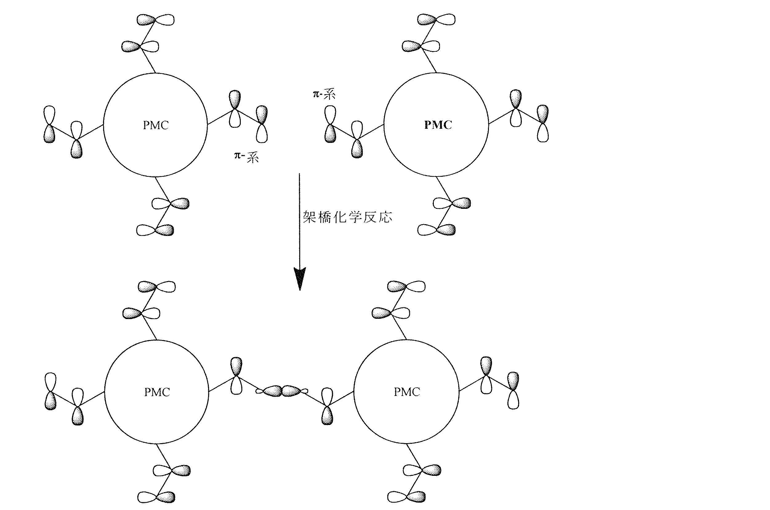
好適には、散乱防止-レジストハイブリッド構成成分の一次金属錯体(複数可)に会合するか、または結合する(好ましくは、供与結合を介して)1つ以上の配位子は、レジスト構成成分(複数可)であるか、またはそれ(ら)を含む。このような配位子は、「レジスト配位子」と呼ばれ得る。したがって、好適には、レジスト配位子は、架橋可能な原子または基(例えば、π系)および配位供与原子または基を含む。1つ以上のこのようなレジスト配位子(複数可)は、散乱防止化合物に関連して、またはそれに加えて、本明細書で定義される任意の他のいずれかの配位子の代わりに、一次金属錯体内に組み込まれてもよい。例えば、一次金属錯体は、レジスト配位子(複数可)と本明細書の他の箇所に記載されている他の配位子(例えば、アルカン酸塩などの非レジスト配位子)との混合物を含んでもよい。 Suitably, the one or more ligands associated with or bound (preferably via dative bonding) to the primary metal complex(s) of the antiscatter-resist hybrid component is the resist component ( is or includes (the). Such ligands may be referred to as "resist ligands." Thus, resist ligands preferably include crosslinkable atoms or groups (eg, π-systems) and coordination donor atoms or groups. One or more such resist ligand(s) may be substituted for any other ligand defined herein in association with or in addition to the anti-scattering compound , may be incorporated within the primary metal complex. For example, the primary metal complex is a mixture of resist ligand(s) and other ligands described elsewhere herein (e.g., non-resist ligands such as alkanoates). may include
好適には、供与原子または基は、孤立電子対担持ヘテロ原子(例えば、好適には窒素および/または酸素原子)、好適には2つ以上の孤立電子対担持ヘテロ原子を含む(これにより供与原子または基を介して配位子の多座が促進される)。例えば、レジスト配位子は、カルボキシレート、カルボン酸エステルまたはカルボン酸基を含むことができ、これは、その各々が一次金属錯体の金属中心と配位可能な孤立電子対を担持する2つの酸素原子を含む。 Preferably, the donor atom or group comprises a lone-pair-bearing heteroatom (e.g., preferably a nitrogen and/or oxygen atom), preferably two or more lone-pair-bearing heteroatoms (thus providing a donor atom or groups to promote polydentation of the ligand). For example, resist ligands can include carboxylate, carboxylic acid ester, or carboxylic acid groups, which are two oxygen atoms each carrying a lone pair of electrons capable of coordinating with the metal center of the primary metal complex. Contains atoms.
好適には、架橋可能な原子または基は、π系、好適には、末端π系、最も好適には末端アルケン基を含む。例えば、レジスト配位子は、末端アルケン基を含むことができる。 Preferably the crosslinkable atoms or groups comprise a π-system, preferably a terminal π-system, most preferably a terminal alkene group. For example, resist ligands can include terminal alkene groups.
好適には、特に、一次金属錯体が多金属性金属ケージまたは他の多金属種である場合、レジスト配位子のうちの少なくとも1つ以上(好適には全て)が、対応する一次金属錯体内で外部的に配位される(すなわち、内側部分の反対側であるケージの外側部分またはケージ内の隙間に存在する)。配位子をこのように並置することは、そうでなければ金属ケージ構造内に存在するレジスト配位子のために妨げられる可能性のある架橋化学反応を促進する。 Preferably, at least one or more (preferably all) of the resist ligands are within the corresponding primary metal complex, particularly when the primary metal complex is a multimetallic metal cage or other multimetallic species. (i.e., present in the outer part of the cage opposite the inner part or in the interstices within the cage). This juxtaposition of ligands promotes cross-linking chemistry that may otherwise be hindered due to resist ligands present within the metal cage structure.
特に好適なレジスト配位子は、任意的に置換されていてもよい:アルケノエート、アルケン酸、アルケン酸エステル、アルケン酸アミド、アルキノエート、アルキン酸、アルキン酸エステル、アルキン酸アミド、またはこれらの混合物からなる群から独立して選択され得る。特定の実施形態では、レジスト配位子(複数可)は、(任意的に置換されていてもよい)アルケノエート、アルケン酸、アルケン酸エステル、アルケン酸アミド、またはこれらの混合物からなる群から選択される。特定の実施形態では、レジスト配位子(複数可)は、(任意的に置換されていてもよい)(2~20C)アルケノエート、(2~20C)アルケン酸、(2~20C)アルケン酸エステル、(2~20C)アルケン酸アミド、またはこれらの混合物からなる群から選択される。特定の実施形態では、レジスト配位子(複数可)は、(任意的に置換されていてもよい)(2~12C)アルケノエート、(2~12C)アルケン酸、(2~12C)アルケン酸エステル、(2~12C)アルケン酸アミド、またはこれらの混合物からなる群から選択される。特定の実施形態では、レジスト配位子(複数可)は、(任意的に置換されていてもよい)(2~6C)アルケノエート、(2~6C)アルケン酸、(2~6C)アルケン酸エステル、(2~6C)アルケン酸アミド、またはこれらの混合物からなる群から選択される。好適には、前述のいずれかのあらゆる任意の置換基は、(関連する条件下で)一次金属錯体内の配位または架橋のいずれをも妨げるものではない。好適には、前述の基のいずれかまたは全ては、少なくとも1つの末端アルケンまたはアルキン部分を含む。 Particularly preferred resist ligands are optionally substituted from : alkenoates, alkenoic acids, alkenoate esters, alkenoamides, alkinoates, alkynoates, alkinate esters, alkinate amides, or mixtures thereof. can be independently selected from the group consisting of In certain embodiments, the resist ligand(s) is selected from the group consisting of (optionally substituted) alkenoates, alkenoic acids, alkenoic acid esters, alkenoic acid amides, or mixtures thereof. be. In certain embodiments, the resist ligand(s) is (optionally substituted ) ( 2-20C ) alkenoate, (2-20C) alkenoic acid, (2-20C) alkenoate , (2-20C) alkenamides, or mixtures thereof. In certain embodiments, the resist ligand(s) are (optionally substituted ) (2-12C)alkenoates, (2-12C)alkenoic acids, (2-12C)alkenoic esters , (2-12C) alkenic acid amides, or mixtures thereof. In certain embodiments, the resist ligand(s) are (optionally substituted ) (2-6C)alkenoates, (2-6C)alkenoic acids, (2-6C)alkenoic esters , (2-6C) alkenic acid amides, or mixtures thereof. Suitably, any optional substituents of any of the foregoing do not (under the relevant conditions) interfere with either coordination or bridging within the primary metal complex. Suitably any or all of the foregoing groups contain at least one terminal alkene or alkyne moiety.
特定の実施形態では、レジスト配位子(複数可)は、1つ以上の孤立電子対担持ヘテロ原子(例えば、Nおよび/またはO)、および1つ以上の末端アルケン基を含む。特定の実施形態では、レジスト配位子(複数可)は、任意により1個以上のヘテロ原子で置換された(2~20C)アルケンを含む。 In certain embodiments, the resist ligand(s) comprise one or more lone pair-bearing heteroatoms (eg, N and/or O) and one or more terminal alkene groups. In certain embodiments, the resist ligand(s) comprise (2-20C) alkenes optionally substituted with one or more heteroatoms.
特定の実施形態では、レジスト配位子(複数可)は、2-メチル-4-ペンテン酸、ジ-アリルアミン、N,Nメチレンビスアクリルアミド(bis-AMD)、またはペンタエリスリトール(pentraerythritol)テトラアクリレートからなる群から選択される。 In certain embodiments, the resist ligand(s) is from 2-methyl-4-pentenoic acid, di-allylamine, N,N methylenebisacrylamide (bis-AMD), or pentraerythritol tetraacrylate. selected from the group consisting of
一次金属錯体は、好適には1~16個のレジスト配位子(またはレジスト構成成分)、好適には2~12個、好適には4~10個を含む。好適には、一次金属錯体は、1~16個のアルケン基(好適には架橋可能なアルケン基)、好適には2~12個、好適には4~10個を含む。 The primary metal complex preferably contains 1-16 resist ligands (or resist constituents), preferably 2-12, preferably 4-10. Preferably, the primary metal complex contains 1 to 16 alkene groups (preferably crosslinkable alkene groups), preferably 2 to 12, preferably 4 to 10.
一次金属錯体は、好適には1つ以上の配位子、好適には一次金属錯体の金属種(例えば、M1および/またはM2)のうちの1つ、それ以上、または全て(または両方)に配位した1つ以上の配位子を含む。好適には、一次金属錯体は、一次金属錯体内の全ての金属種(好適には間接的に、好適には供与結合を介して)を一緒に結合させるのに十分な種類および十分な数の配位子(配位子の混合物を含む)を含み、好適には金属ケージを形成し、好適にはいかなる金属-金属結合も伴わない。このようなものとして、一次金属錯体は、好適には、2つ以上の金属種の間に橋架けを提供することができる、1つ以上の橋架け配位子を好適に含み、このような橋架け配位子は、二座などの多座であってもよいが、フルオロまたは酸素ベースの配位子などの電子が2つ以上の孤立電子対を供与することができる単座であってもよい。最も好適には、一次金属錯体は、2つ以上の異なる種類の配位子の混合物を含み、好適には、その種類の配位子の一方は二座であり、他方は単座である。最も好適には、一次金属錯体内の配位子の全ては、2つ以上の孤立電子対を供与できる配位原子を有する。好適には、一次金属錯体は、十分な種類および数の配位子を含み(フルオロなどの単座配位子とカルボキシレートなどの二座配位子との混合物であってもよい)、錯体内の個々の金属種当たり少なくとも平均3個の供与結合(例えば、錯体内の個々のM1およびM2種はそれぞれ、錯体に会合する配位子と少なくとも平均3つの供与結合を形成する)、好適には少なくとも4つの供与結合、最も好適には約6の供与結合が得られる。好適には、全ての金属種の配位部位は、(例えば、特に一次金属錯体が全体の散乱防止化合物内のルイス基として機能することが意図される場合)錯体内の配位子によって完全に充填/飽和されてもよく、または(例えば、特に一次金属錯体が全体の散乱防止化合物内のルイス酸として機能することが意図される場合)金属種の中の1つ以上の空の配位部位であってもよい。 The primary metal complex preferably comprises one or more ligands, preferably one, more or all (or both) of the metal species (e.g. M 1 and/or M 2 ) of the primary metal complex. ) with one or more ligands. Preferably, the primary metal complexes are of a sufficient variety and sufficient number to bind together all metal species (preferably indirectly, preferably via dative bonds) within the primary metal complex. It contains ligands (including mixtures of ligands), preferably forming metal cages, preferably without any metal-metal bonding. As such, the primary metal complex suitably comprises one or more bridging ligands capable of providing a bridge between two or more metal species, such Bridging ligands may be polydentate, such as bidentate, but may also be monodentate, such as fluoro- or oxygen-based ligands, where electrons can donate two or more lone electron pairs. good. Most preferably, the primary metal complex comprises a mixture of two or more different ligand types, preferably one of the ligand types is bidentate and the other is monodentate. Most preferably, all of the ligands in the primary metal complex have coordinating atoms capable of donating more than one lone pair of electrons. Suitably, the primary metal complex contains a sufficient type and number of ligands (which may be a mixture of monodentate ligands such as fluoro and bidentate ligands such as carboxylates) such that the intracomplex an average of at least 3 dative bonds per individual metal species (e.g., each individual M1 and M2 species in the complex forms at least an average of 3 dative bonds with ligands associated with the complex), preferably provides at least 4 dative bonds, most preferably about 6 dative bonds. Preferably, all metal species coordination sites are fully occupied by ligands within the complex (e.g., particularly when the primary metal complex is intended to function as a Lewis group within the overall antiscattering compound). one or more vacant coordination sites in the metal species, which may be filled/saturated, or (e.g., especially if the primary metal complex is intended to function as a Lewis acid within the overall antiscattering compound) may be
好適には、少なくともいくつかの、好適には全ての配位子が負に荷電しており、最も好適には単一の負電荷を担持する。好適には、一次金属錯体の配位子(複数可)の共役酸は、(標準周囲温度および圧力での水中において)2以上、好適には3以上のpKa値を有する。 Preferably at least some, preferably all ligands are negatively charged and most preferably carry a single negative charge. Preferably, the conjugate acid of the ligand(s) of the primary metal complex has a pKa value (in water at standard ambient temperature and pressure) of 2 or greater, preferably 3 or greater.
好適には、一次金属錯体の配位子(複数可)は、単座配位子、二座配位子、またはこれらの混合物(複数可)から選択される。最も好適には、一次金属錯体の配位子(複数可)は、単座配位子と二座配位子との混合物を含む。 Suitably, the ligand(s) of the primary metal complex are selected from monodentate ligands, bidentate ligands or mixture(s) thereof. Most preferably, the ligand(s) of the primary metal complex comprise a mixture of monodentate and bidentate ligands.
単座配位子(複数可)は、好適には、2つ以上の孤立電子対、最も好適にはフッ化物を担持する配位原子(複数可)(それに対して供与結合が金属種で形成される原子および/またはそれから供与結合が形成される原子)を有する。 The monodentate ligand(s) is preferably a coordinating atom(s) bearing two or more lone electron pairs, most preferably fluoride, to which a dative bond is formed with the metal species. and/or atoms from which dative bonds are formed).
二座配位子は、好適には、2つ以上の孤立電子対を担持する少なくとも1つ、より好適には2つの配位原子、最も好適にはカルボキシレート(例えば、任意的に置換されていてもよい有機カルボキシレート、例えば、アセテート、ピバレート、3,3-ジメチルブタノエート、ベンゾエート、4-tert-ブチルベンゾエート、イソニコチネートなど任意的に置換されていてもよいヒドロカルビルカルボキシレートなど)を有する。いくつかの実施形態(特に、一次金属錯体がルイス塩基として機能することが意図される場合)では、一次金属錯体の配位子は、少なくとも2つの異なる種類の二座配位子(例えば第1および第2の二座配位子を含む)またはカルボキシレート配位子を含む。このような実施形態では、好適には、二座配位子のうちの少なくとも1つ(例えば、第2の配位子)は、一次金属錯体内に金属種との内部供与結合(複数可)を形成することができる配位原子(複数可)と、別の(異なる)錯体またはケージの金属種との外部供与結合を形成することができる1つ以上の追加の配位原子を含む。好適には、このような二官能性配位子(例えば、第2の二座配位子)は、カルボキシレート基および追加の酸素または窒素含有部分、好ましくは窒素含有部分を含み得、その例としてはイソニコチネートおよび4-アミノベンゾエートが挙げられる。しかし、いくつかの実施形態(特に、一次金属錯体がルイス酸として機能することが意図される場合)では、一次金属錯体の配位子は、別の(異なる)錯体またはケージの金属種との外部供与結合を形成することができるいずれの追加の配位原子も含まず、また、好適には、1つのタイプの二座配位子またはカルボキシレート配位子を含み得る。 Bidentate ligands preferably have at least one, more preferably two coordinating atoms, most preferably carboxylate (e.g., optionally substituted optionally substituted hydrocarbyl carboxylates such as acetate, pivalate, 3,3-dimethylbutanoate, benzoate, 4-tert-butylbenzoate, isonicotinate , etc.). have. In some embodiments (particularly where the primary metal complex is intended to function as a Lewis base), the ligands of the primary metal complex are at least two different types of bidentate ligands (e.g., primary and a second bidentate ligand) or a carboxylate ligand. In such embodiments, preferably at least one of the bidentate ligands (e.g., the second ligand) has internal dative bond(s) with the metal species within the primary metal complex. and one or more additional coordinating atoms capable of forming an external dative bond with another (different) complex or cage metal species. Suitably such bifunctional ligands (e.g., second bidentate ligands) may include carboxylate groups and additional oxygen- or nitrogen-containing moieties, preferably nitrogen-containing moieties, such as These include isonicotinate and 4-aminobenzoate. However, in some embodiments (particularly where the primary metal complex is intended to function as a Lewis acid), the ligand of the primary metal complex is a metal species of another (different) complex or cage. It does not contain any additional coordinating atoms capable of forming external dative bonds and may suitably contain one type of bidentate or carboxylate ligand.
特定の実施形態では、一次金属錯体は、式Iによって定義されるか、または式Iによって定義される単位を含む:
[M1
xM2
y…Mn
zn(monoLIG1)m1(monoLIG2)m2…(monoLIGq)mq(biLIG1)b1(biLIG2)b2…(biLIGr)br(optLIGs)(optLIG1)o1(optLIG2)o2…(optLIGs)os];
または
以下のものを含む、本質的になる、または以下のものを一緒に混合すること、反応させること、もしくは他の方法で組み合わせることによって形成されると定義される(一次金属錯体の各モル当たり):
-xモルの第1の金属種(M1)、
-yモルの第2の金属種(M2)、
-任意によりznモルの各追加のn番目の金属種(Mn)、
-m1モルの第1の単座配位子(monoLIG1)、
-任意によりm2モルの第2の単座配位子(monoLIG2)、
-任意によりmqモルのそれぞれの追加のq番目の単座配位子(monoLIGq)、
-b1モルの第1の二座配位子(biLIG1)、
-任意によりb2モルの第2の二座配位子(biLIG2)、
-任意によりbrモルの各追加のr番目の二座配位子(biLIGr)、
-o1モルの第1の任意の余剰/末端配位子(optLIG1)、
-o2モルの第2の任意の余剰/末端配位子(optLIG2)、
-osモルのそれぞれの追加の任意の第s番目の余剰/末端配位子(optLIGs)、
式中:
M1は好適には本明細書で定義される第1の金属種(最も好適には三価の金属イオン、例えばCr3+)であり、
M2は、好適には本明細書で定義される第2の金属種(最も好適には二価の金属イオン、例えばNi2+)であり、
Mnは、好適には本明細書で定義されるn番目の金属種であり(最も好適には存在しない)、
monoLIG1は、好適には本明細書で定義される第1の単座配位子(最も好適にはその共役酸がpKa≧2を有するモノアニオン、好適にはフッ化物)であり、
monoLIG2は、好適には本明細書で定義される(最も好適には存在しない)第2の単座配位子であり、
monoLIGqは、好適には本明細書で定義される(最も好適には存在しない)q番目の単座配位子であり、
biLIG1は、好適には、本明細書で定義される第1の二座配位子(最も好適にはカルボキシエート(carboxyate)であり、好適には、いずれの追加のヘテロ原子も存在しない)であり、
biLIG2は、好適には本明細書で定義される第2の二座配位子(最も好適には存在しないか、または追加の酸素または窒素含有部分、最も好ましくは追加の窒素含有部分を担持するカルボキシレート)であり、
biLIGrは、好適には本明細書で定義される(最も好適には存在しない)r番目の二座配位子であり、
optLIG1は、好適には本明細書で定義される(最も好適には存在しないか、またはd=6のN-メチル-D-グルカミンなどの配座数dの多座配位子であり、溶媒、またはカルボン酸である)第1の任意の余剰な配位子(好適には配座数dを有する)であり、
optLIG2は、好適には本明細書で定義される(最も好適には存在しないか、または溶媒またはカルボン酸である)第2の任意の余剰/末端配位子であり、
optLIGsは、好適には本明細書で定義される(最も好適には存在しないか、または溶媒またはカルボン酸である)s番目の任意の余剰/末端配位子である。
In certain embodiments, the primary metal complex is defined by Formula I or comprises units defined by Formula I:
[M 1 x M 2 y... Mnzn ( monoLIG 1 ) m1 (monoLIG 2 ) m2... (monoLIG q ) mq (biLIG 1 ) b1 (biLIG 2 ) b2... (biLIG r ) br (optLIG s ) (optLIG 1 ) o1 (optLIG 2 ) o2 ... (optLIG s ) os ];
or defined as comprising, consisting essentially of, or formed by mixing, reacting, or otherwise combining together (for each mole of primary metal complex) ):
- x moles of the first metal species (M 1 ),
- y moles of second metal species (M 2 ),
- optionally z n moles of each additional n-th metal species (M n ),
-m moles of the first monodentate ligand (monoLIG 1 ),
- optionally m2 moles of a second monodentate ligand (monoLIG 2 ),
- optionally mq moles of each additional q-th monodentate ligand (monoLIG q ),
-
- optionally b2 molar second bidentate ligand (biLIG 2 ),
- optionally br moles of each additional r-th bidentate ligand (biLIG r ),
-
- o2 molar second optional excess/terminal ligand (optLIG 2 ),
- each additional optional s th excess/terminal ligand (optLIG s ) of the osmol;
In the formula:
M 1 is preferably a first metal species as defined herein (most preferably a trivalent metal ion such as Cr 3+ );
M2 is preferably a second metal species as defined herein (most preferably a divalent metal ion such as Ni2 + ),
Mn is preferably the nth metal species as defined herein (most preferably absent),
monoLIG 1 is preferably the first monodentate ligand defined herein (most preferably a monoanion whose conjugate acid has a pKa≧2, preferably a fluoride);
monoLIG 2 is preferably a (most preferably absent) second monodentate ligand as defined herein,
monoLIG q is preferably the (most preferably absent) qth monodentate ligand as defined herein,
biLIG 1 is preferably the first bidentate ligand (most preferably a carboxylate, preferably absent any additional heteroatoms) as defined herein and
biLIG 2 preferably carries a second bidentate ligand as defined herein (most preferably absent or carrying additional oxygen- or nitrogen-containing moieties, most preferably additional nitrogen-containing moieties carboxylate),
biLIG r is preferably the (most preferably absent) r-th bidentate ligand as defined herein,
optLIG 1 is preferably as defined herein (most preferably absent or a multidentate ligand of d-coordination such as N-methyl-D-glucamine with d=6, a solvent, or a carboxylic acid) first any excess ligand (preferably having a dentation number d);
optLIG 2 is preferably a second optional excess/terminal ligand (most preferably absent or solvent or carboxylic acid) as defined herein,
optLIG s is preferably the sth optional excess/terminal ligand (most preferably absent or solvent or carboxylic acid) as defined herein.
最も好適には、x、y、zn、m1、m2、mq、b1、b2、br、o1、o2、osは、0であるか、または整数であるが、いくつかの例では、これらのうちのいずれか、いくつか、または全てが0と1との中間値または任意の2つの整数の間の中間値を有し得る。 Most preferably, x, y, zn, m1, m2, mq, b1, b2, br, o1, o2, os are 0 or integers, although in some examples may have intermediate values between 0 and 1 or between any two integers.
好適には、xは、1~16の数(最も好適には整数)、好適には4~10、より好適には2~8、好適には7である。 Preferably x is a number from 1 to 16 (most preferably an integer), preferably from 4 to 10, more preferably from 2 to 8, preferably 7.
好適には、yは、0~15の数(最も好適には整数)、好適には0~7であり、好適には0~2、好適には0または1、最も好適には1である。 Preferably y is a number from 0 to 15 (most preferably an integer), preferably 0 to 7, preferably 0 to 2, preferably 0 or 1, most preferably 1 .
znは、好適には0~14、好適には0~6、好適には0~2、好適には0の数(最も好適には整数)である。 zn is preferably a number from 0 to 14, preferably 0 to 6, preferably 0 to 2, preferably 0 (most preferably an integer).
m1は、好適には0~40の数(最も好適には整数)であり、好適には0~20または0~10、好適には1~20、好適には2~12、好適には4~10、好適には8である。 m1 is preferably a number from 0 to 40 (most preferably an integer), preferably 0 to 20 or 0 to 10, preferably 1 to 20, preferably 2 to 12, preferably 4 ~10, preferably 8.
m2は、好適には0~39の数(最も好適には整数)であり、好適には0~18、好適には0~10、好適には0~2、好適には0である。 m2 is preferably a number from 0 to 39 (most preferably an integer), preferably 0 to 18, preferably 0 to 10, preferably 0 to 2, preferably 0.
mqは、好適には0~38の数(最も好適には整数)であり、好適には0~17、好適には0~9、好適には0~2、好適には0である。 mq is preferably a number from 0 to 38 (most preferably an integer), preferably 0 to 17, preferably 0 to 9, preferably 0 to 2, preferably 0.
b1は、好適には0~20の数(最も好適には整数)であり、好適には1~20、好適には1~16、好適には12~16、好適には12~15、好適には15または16である。 b1 is preferably a number from 0 to 20 (most preferably an integer), preferably from 1 to 20, preferably from 1 to 16, preferably from 12 to 16, preferably from 12 to 15, preferably is 15 or 16.
b2は、好適には0~20の数(最も好適には整数)であり、好適には0~16、好適には0~8、好適には0~3、好適には1~4、好適には0または1である。 b2 is preferably a number from 0 to 20 (most preferably an integer), preferably from 0 to 16, preferably from 0 to 8, preferably from 0 to 3, preferably from 1 to 4, preferably is 0 or 1.
brは、好適には0~19の数(最も好適には整数)であり、好適には0~15、好適には0~7、好適には0~2、好適には0である。 br is preferably a number from 0 to 19 (most preferably an integer), preferably 0 to 15, preferably 0 to 7, preferably 0 to 2, preferably 0.
好適には、o1は、0~8の数(最も好適には整数)、好適には0~4、好適には0または1、最も好適には0である。 Preferably o1 is a number from 0 to 8 (most preferably an integer), preferably 0 to 4, preferably 0 or 1, most preferably 0.
好適には、o2は、0~7の数(最も好適には整数)、好適には0~3、好適には0または1、最も好適には0である。 Preferably o2 is a number from 0 to 7 (most preferably an integer), preferably 0 to 3, preferably 0 or 1, most preferably 0.
好適には、osは、0~6の数(最も好適には整数)、好適には0~2、好適には0または1、最も好適には0である。 Preferably, os is a number from 0 to 6 (most preferably an integer), preferably 0 to 2, preferably 0 or 1, most preferably 0.
一実施形態では、一次金属錯体は、式Iによって定義されるか、または式Iによって定義される単位を含む:
[M1
xM2
y…Mn
zn(monoLIG1)m1(monoLIG2)m2…(monoLIGq)mq(biLIG1)b1(biLIG2)b2…(biLIGr)br(optLIGs)(optLIG1)o1(optLIG2)o2…(optLIGs)os];
式中:
M1は第1の金属種であり、xは一次金属錯体1モル当たりのM1のモル数であり、xは1~16の数であり、
M2は第2の金属種であり、yは一次金属錯体1モル当たりのM2のモル数であり、yは0~7の数であり、
Mnはn番目の金属種であり、znは一次金属錯体1モル当たりの各Mnのモル数であり、znは0~6の数であり、好適には0~2であり、好適には0である。
monoLIG1は第1の単座配位子であり、m1は一次金属錯体1モル当たりのmonoLIG1のモル数であり、m1は0~20の数であり、
monoLIG2は第2の単座配位子であり、m2は一次金属錯体1モル当たりのmonoLIG2のモル数であり、m2は0~10の数であり、
monoLIGqはq番目の単座配位子であり、mqは一次金属錯体1モル当たりの各monoLIGqのモル数であり、mqは0~2の数であり、
biLIG1は第1の二座配位子であり、b1は一次金属錯体1モル当たりのbiLIG1のモル数であり、b1は1~20の数であり、
biLIG2は第2の二座配位子であり、b2は一次金属錯体1モル当たりのbiLIG2のモル数であり、b2は0~16の数であり、
biLIGrはr番目の二座配位子であり、brは一次金属錯体1モル当たりの各追加のbiLIGrのモル数であり、brは0~2の数であり、
optLIG1は第1の任意の余剰の配位子であり、o1は一次金属錯体1モル当たりのoptLIG1のモル数であり、o1は0~4の数であり、
optLIG2は、第2の任意の余剰/末端配位子であり、o2は、一次金属錯体1モル当たりのoptLIG2のモル数であり、o2は0~3の数であり、
optLIGsは、s番目の任意の余剰/末端配位子であり、osは、一次金属錯体1モル当たりの各追加の任意のoptLIGsのモル数であり、osは0~2の数である。
In one embodiment, the primary metal complex is defined by Formula I or comprises units defined by Formula I:
[M 1 x M 2 y... Mnzn ( monoLIG 1 ) m1 (monoLIG 2 ) m2... (monoLIG q ) mq (biLIG 1 ) b1 (biLIG 2 ) b2... (biLIG r ) br (optLIG s ) (optLIG 1 ) o1 (optLIG 2 ) o2 ... (optLIG s ) os ];
In the formula:
M 1 is the first metal species, x is the number of moles of M 1 per mole of the primary metal complex, x is a number from 1 to 16,
M2 is the second metal species, y is the number of moles of M2 per mole of the primary metal complex, y is a number from 0 to 7,
Mn is the nth metal species, zn is the number of moles of each Mn per mole of primary metal complex, zn is a number from 0 to 6, preferably from 0 to 2, preferably is 0.
monoLIG 1 is the first monodentate ligand, m is the number of moles of monoLIG 1 per mole of the primary metal complex, m is a number from 0 to 20,
monoLIG 2 is the second monodentate ligand, m is the number of moles of monoLIG 2 per mole of the primary metal complex, m is a number from 0 to 10,
monoLIG q is the qth monodentate ligand, mq is the number of moles of each monoLIG q per mole of the primary metal complex, mq is a number from 0 to 2,
biLIG 1 is the first bidentate ligand, b1 is the number of moles of biLIG 1 per mole of primary metal complex, b1 is a number from 1 to 20,
biLIG 2 is a second bidentate ligand, b2 is the number of moles of biLIG 2 per mole of primary metal complex, b2 is a number from 0 to 16,
biLIG r is the r-th bidentate ligand, br is the number of moles of each additional biLIG r per mole of primary metal complex, br is a number from 0 to 2,
optLIG 1 is the first optional extra ligand, o1 is the number of moles of optLIG 1 per mole of primary metal complex, o1 is a number from 0 to 4,
optLIG 2 is the second optional excess/terminal ligand, o2 is the number of moles of optLIG2 per mole of primary metal complex, o2 is a number from 0 to 3,
optLIG s is the sth optional extra/terminal ligand, os is the number of moles of each additional optional optLIG s per mole of primary metal complex, and os is a number from 0 to 2 .
一実施形態では、一次金属錯体は、式Iaによって定義されるか、または式Iによって定義される単位を含む:
[M1
xM2
y(monoLIG1)m1(biLIG1)b1(biLIG2)b2];
式中:
M1は第1の金属種であり、xは一次金属錯体1モル当たりのM1のモル数であり、xは4~10の数であり、
M2は第2の金属種であり、yは一次金属錯体1モル当たりのM2のモル数であり、yは0~2の数であり、
monoLIG1は第1の単座配位子であり、m1は一次金属錯体1モル当たりのmonoLIG1のモル数であり、m1は4~10の数であり、
biLIG1は第1の二座配位子であり、b1は一次金属錯体1モル当たりのbiLIG1のモル数であり、b1は12~16の数であり、
biLIG2は第2の二座配位子であり、b2は一次金属錯体1モル当たりのbiLIG2のモル数であり、b2は0~3の数である。
In one embodiment, the primary metal complex is defined by Formula Ia or comprises units defined by Formula I:
[M 1 x M 2 y (monoLIG 1 ) m1 (biLIG 1 ) b1 (biLIG 2 ) b2 ];
In the formula:
M 1 is the first metal species, x is the number of moles of M 1 per mole of the primary metal complex, x is a number from 4 to 10,
M2 is the second metal species, y is the number of moles of M2 per mole of the primary metal complex, y is a number from 0 to 2,
monoLIG 1 is the first monodentate ligand, m is the number of moles of monoLIG 1 per mole of the primary metal complex, m is a number from 4 to 10,
biLIG 1 is the first bidentate ligand, b1 is the number of moles of biLIG 1 per mole of primary metal complex, b1 is a number from 12 to 16,
biLIG 2 is the second bidentate ligand, b2 is the number of moles of biLIG 2 per mole of primary metal complex, and b2 is a number from 0-3.
好適には、xとyの合計は少なくとも2、より好適には少なくとも3、好適には少なくとも4、好適には少なくとも5、好適には少なくとも6、好適には少なくとも7、好適には約8である。好適には、xとyの合計は多くとも16、好適には多くとも12、好適には多くとも10である。好適には、xは少なくとも4であり、好適には少なくとも6であり、好適には多くとも10であり、最も好適には約7である。特定の実施形態では、yは0である(すなわち、第2の金属種が全くない)が、好ましくはyは0ではなく、好適には少なくとも1であり、最も好適には約1である。最も好適には、xは7+/-δ(すなわち、δは多くともxの10%、好適には多くともxの1%)であり、yは1-/+δである。特定の実施形態では、M1はCr3+であり、M2はNi2+であり、xとyの合計は7~10であり、xは6~10である。特定の実施形態では、M1はCr3+であり、M2はNi2+であり、xは約7であり、yは約1である。 Preferably, the sum of x and y is at least 2, more preferably at least 3, preferably at least 4, preferably at least 5, preferably at least 6, preferably at least 7, preferably about 8. be. Preferably, the sum of x and y is at most 16, preferably at most 12, preferably at most 10. Preferably x is at least 4, preferably at least 6, preferably at most 10 and most preferably about 7. In certain embodiments, y is 0 (ie, no second metal species), but preferably y is not 0, preferably at least 1, and most preferably about 1. Most preferably x is 7+/-δ (ie δ is at most 10% of x, preferably at most 1% of x) and y is 1-/+δ. In certain embodiments, M 1 is Cr 3+ , M 2 is Ni 2+ , the sum of x and y is 7-10, and x is 6-10. In certain embodiments, M 1 is Cr 3+ , M 2 is Ni 2+ , x is about 7 and y is about 1.
最も好適には、一次金属錯体は、第1の金属種(M1)および任意により第2の金属種(M2)を超えたさらなる金属種を含まず、したがってznは0である。しかし、いくつかの例では、一次金属錯体を、例えば、少量の代替的金属種でドープして、散乱防止化合物の特性を慎重に変えてもよい。このような実施形態では、任意のまたは全てのzn値(z3+z4+…+zn)の合計は、好適にはxとyの合計未満であり、好適には少なくとも5倍少なく(すなわちx+yの合計の多くとも5倍)、好適には少なくとも10倍少なく、好適には少なくとも100倍少ない。 Most preferably, the primary metal complex contains no further metal species beyond the first metal species (M 1 ) and optionally the second metal species (M 2 ), so zn is zero. However, in some instances the primary metal complex may be doped, for example, with minor amounts of alternative metal species to deliberately alter the properties of the anti-scattering compound. In such embodiments, the sum of any or all zn values (z3+z4+...+zn) is preferably less than the sum of x and y, preferably at least 5 times less (i.e., the sum of x+y is at most 5 times), preferably at least 10 times less, preferably at least 100 times less.
好適には、
-(m1+m2…+mq)の合計(すなわち、錯体1モル当たりの単座配位子(複数可)のモルの合計)、
-2×(b1+b2+…+bq)(すなわち、錯体1モル当たりの二座配位子(複数可)のモルの合計の2倍)、
-o1×d(すなわち、錯体1モル当たりの任意の余剰な配位子(複数可)のモル数のd倍)は、
50以下、好適には42以下、好適には40以下、好適には30以上、好適には38以上、好適には約40である。
Preferably,
- sum of (m1+m2...+mq) (i.e. sum of moles of monodentate ligand(s) per mole of complex),
−2×(b1+b2+...+bq) (i.e. twice the sum of moles of bidentate ligand(s) per mole of complex),
−o1×d (i.e., d times the number of moles of any excess ligand(s) per mole of complex) is
50 or less, preferably 42 or less, preferably 40 or less, preferably 30 or more, preferably 38 or more, preferably about 40.
好適には、m1、m2、…、およびmqの合計は、少なくとも1、好適には少なくとも2、好適には少なくとも3、好適には少なくとも6、好適には多くとも7、好適には多くとも16、好適には多くとも12、好適には多くとも10、最も好適には約8である。好ましい実施形態では、第1の単座配位子を超える単座配位子は存在しない(すなわち、m2およびmqは双方とも0である)。特定の実施形態では、monoLIG1はフッ化物(F)である。特定の実施形態では、monoLIG1はフッ化物(F)であり、m1は2~9であり、m2およびmqは全て0であり、好適にはM1はCr3+であり、M2はNi2+であり、xとyの合計は7~10であり、xは6~10である。特定の実施形態では、monoLIG1はフッ化物(F)であり、m1は3であり、m2およびmqは全て0である(すなわち、他の単座配位子はない)。特定の実施形態では、monoLIG1はフッ化物(F)であり、m1は8であり、m2およびmqは全て0である(すなわち、他の単座配位子はない)。 Preferably the sum of m1, m2, ... and mq is at least 1, preferably at least 2, preferably at least 3, preferably at least 6, preferably at most 7, preferably at most 16 , preferably at most 12, preferably at most 10, most preferably about 8. In preferred embodiments, there are no monodentate ligands beyond the first monodentate ligand (ie, m2 and mq are both 0). In certain embodiments, monoLIG 1 is fluoride (F). In certain embodiments, monoLIG 1 is fluoride (F), m1 is 2-9, m2 and mq are all 0 , preferably M1 is Cr3+, M2 is Ni2 + and the sum of x and y is 7-10 and x is 6-10. In certain embodiments, monoLIG 1 is fluoride (F), m1 is 3, and m2 and mq are all 0 (ie, no other monodentate ligands). In certain embodiments, monoLIG 1 is fluoride (F), m1 is 8, and m2 and mq are all 0 (ie, no other monodentate ligands).
好適には、b1、b2、…、およびbrの合計は、少なくとも6、好適には少なくとも10、好適には少なくとも14、好適には多くとも22、好適には多くとも20、好適には多くとも18、最も好適には約16である。いくつかの実施形態では、第1および第2の二座配位子を超える二座配位子(すなわち、brは全てが0である)は存在せず、いくつかの実施形態では、第1の二座配位子を超える二座配位子は存在しない(すなわち、b2およびbrは双方とも0である)。一実施形態では、biLIG1は、式-O2CRB1(またはRB1CO2
-)によって定義されるカルボキシレートであり、RB1は好適には、ヒドロカルビル部分(好適には、塩基またはキレート基がないヒドロカルビル部分)などの基(任意により置換基)であり、好適には、(1~12C)アルキル、(1~12C)アルケニル、(1~12C)アルキニル、(3~8C)シクロアルキル、(3~8C)シクロアルケニル、(1~3C)アルキル(3~8C)シクロアルキル、(1~3C)アルキル(3~8C)シクロアルケニル、アリール、(1~3C)アルキルアリール、アリール(1~3C)アルキルから選択される。好適には、RB1は、(1~12C)アルケニル、(1~12C)アルキニル、(3~8C)シクロアルケニル、アリール、(1~3C)アルキルアリールまたはアリール(1~3C)アルキルである。最も好適にはRB1は(1~5C)アルケニルである。一実施形態では、biLIG2は、式-O2CRB2(またはRB2CO2
-)によって定義されるカルボン酸塩であり、好適には、RB2は、塩基またはキレート基(例えば、供与結合を形成するために自由に配位する孤立電子対を有する部分)を含む基であり、好適には、任意により置換されるヘテロシクリル、ヘテロアリール、ヘテロシクリル(1~6C)アルキル、ヘテロアリール(1~6C)アルキルから選択されるか、または(1~12C)アルキル、(1~12C)アルケニル、(1~12C)アルキニル、(3~8C)シクロアルキル、(3~8C)シクロアルケニル、(1~3C)アルキル(3~8C)シクロアルキル、(1~3C)アルキル(3~8C)シクロアルケニル、アリール、(1~3C)アルキルアリールまたはアリール(1~3C)アルキルから選択され、例えば、アミノ、アルキルアミノ、ジアルキルアミノ、ヒドロキシル、(1~6C)アルコキシ、カルボニル、イミノ、チオ、チオカルボニルなどの1つ以上の塩基またはキレート基によって置換される。最も好適には、RB2はピリジル、アミノフェニル、N-(1~3C)アルキルアミノフェニル、N,N-ジ(1~3C)アルキルアミノフェニル、最も好適にはピリジルであり、最も好適には4-ピリジルであり、最も好適にはbiLIG2はイソニコチネートである。特定の実施形態では、biLIG1は、任意的に置換されていてもよいヒドロカルビルカルボキシレート(例えば、ピバレートなどの(1~6C)アルキルカルボキシレート)であり、biLIG2は、少なくとも1つの追加のヘテロ原子を担持する有機または任意的に置換されていてもよいヒドロカルビルカルボキシレート(例えば、錯体の外部の金属種をキレートするためのルイス塩基または配位子として作用できるもの、例えばイソニコチネート)であり、b1は12~20(最も好適には14~18、最も好適には15~16)であり、b2は0~4(最も好適には0または1~3)であり、好適にはM1はCr3+であり、M2はNi2+であり、xとyの合計は7~10であり、xは6~10であり、好適にはmonoLIG1はフッ化物(F)であり、m1は2~9であり、m2およびmqは全て0である。
Preferably the sum of b1, b2, ... and br is at least 6, preferably at least 10, preferably at least 14, preferably at most 22, preferably at most 20, preferably at most 18, most preferably about 16. In some embodiments, there are no bidentate ligands beyond the first and second bidentate ligands (i.e., br are all 0); (ie, b2 and br are both 0). In one embodiment, biLIG 1 is a carboxylate defined by the formula —O 2 CR B1 (or R B1 CO 2 − ), where R B1 is preferably a hydrocarbyl moiety (preferably a base or chelating group (optionally substituted hydrocarbyl moieties), preferably (1-12C)alkyl, (1-12C)alkenyl, (1-12C)alkynyl, (3-8C)cycloalkyl, (3-8C) cycloalkenyl, (1-3C) alkyl(3-8C) cycloalkyl, (1-3C) alkyl(3-8C) cycloalkenyl, aryl, (1-3C) alkylaryl, aryl (1- 3C) selected from alkyl; Suitably,
好適には、o1、o2、…、およびosの合計は、0~4、好適には0~2、最も好適には0~1である。いくつかの実施形態では、第1の任意の余剰/末端配位子を超える任意の余剰/末端配位子は存在しない(すなわち、全てのo2およびosが0である)。特定の実施形態では、o1、o2、…、およびosの合計は、0である(すなわち、実質的に任意の余剰/末端配位子は存在しない)。1つ以上の任意の余剰/末端配位子が存在する場合、これらは、H2O、テトラヒドロフラン、ピリジンなどの溶媒分子(単座、二座、または他の多座)を含んでもよい。特定の実施形態では、一次金属錯体は、3以上、好適には4以上、しかしながら好適には多くとも6の配座数を有する多座配位子である少なくとも1つの余剰/末端配位子を含む。このような多座は、例えば、N-(1~6C)アルキル-D-グルカミン(例えば、N-メチル-D-グルカミン)を含み得る。特定の実施形態では、optLIG1は、式Gluc-NH-RO1によって定義され、Gluc-NH-RO1がN-(1~8C)アルキル-D-グルカミンまたはその脱プロトン化形態であり、好適にはRO1が(1~8C)アルキル、より好適には(1~2C)アルキル(例えばメチルまたはエチル)である。このような実施形態では、好適にはo1は1であり、o2および全てのosは0である。
Preferably, the sum of o1, o2, . . . and os is 0-4, preferably 0-2, most preferably 0-1. In some embodiments, there are no extra/terminal ligands beyond the first optional extra/terminal ligand (ie, all o2 and os are 0). In certain embodiments, the sum of o1, o2, ..., and os is 0 (ie, substantially no extra/terminal ligands are present). If one or more optional extra/terminal ligands are present, these may include solvent molecules (monodentate, bidentate, or other polydentate) such as H2O , tetrahydrofuran, pyridine, and the like. In a particular embodiment, the primary metal complex has at least one extra/terminal ligand that is a multidentate ligand having a coordination number of 3 or more, preferably 4 or more, but preferably at most 6. include. Such polydentates can include, for example, N-(1-6C)alkyl-D-glucamines (eg, N-methyl-D-glucamine). In certain embodiments, optLIG 1 is defined by the formula Gluc-NH-R O1 , wherein Gluc-NH-R O1 is N-(1-8C)alkyl-D-glucamine or a deprotonated form thereof;
特定の実施形態では、一次金属錯体は、式IIによって定義されるか、または式IIによって定義される単位を含む:
[M1
xM2
y(monoLIG1)m1(O2CRB1)16-b2(O2CRB2)b2]
式中:
M1は、本明細書で定義される三価の金属イオンであり、最も好適にはCr3+であり、
M2は、本明細書で定義される二価の金属イオンであり、最も好適にはNi2+であり、
xは、本明細書で定義されているとおりであり(好適にはxは6、7、8または9であり、最も好適にはxは7である)、
yは本明細書で定義されているとおりであり(好適には1または2であり、最も好適にはyは1であるが、0であってもよく、ホモ金属の多金属錯体を形成する場合は、同じ酸化状態の金属、例えばCr(III)を有する)、
monoLIG1は、本明細書で定義されるとおりであり(最も好適には、monoLIG1は、フッ化物、Fである)、
m1は本明細書で定義したとおりであり(最も好適にはm1は8である)、
RB1は、本明細書で定義されたとおりであるが、RB1は、好適には、塩基またはキレート基を含まない基であり、好適には、(1~12C)アルキル、(1~12C)アルケニル、(1~12C)アルキニル、(3~8C)シクロアルキル、(3~8C)シクロアルケニル、(1~3C)アルキル(3~8C)シクロアルキル、(1~3C)アルキル(3~8C)シクロアルケニル、アリール、(1~3C)アルキルアリール、アリール(1~3C)アルキルから選択され、
RB2は、本明細書で定義されたとおりであるが、好適には、塩基またはキレート基(例えば、供与結合を形成するために自由に配位結合している孤立電子対を有する部分)を含む基であり、好適には、任意的に置換されていてもよいヘテロシクリル、ヘテロアリール、ヘテロシクリル(1~6C)アルキル、ヘテロアリール(1~6C)アルキルから選択されるか、または(1~12C)アルキル、(1~12C)アルケニル、(1~12C)アルキニル、(3~8C)シクロアルキル、(3~8C)シクロアルケニル、(1~3C)アルキル(3~8C)シクロアルキル、(1~3C)アルキル(3~8C)シクロアルケニル、アリール、(1~3C)アルキルアリールもしくはアリール(1~3C)アルキルから選択され、例えば、アミノ、アルキルアミノ、ジアルキルアミノ、ヒドロキシル、(1~6C)アルコキシ、カルボニル、イミノ、チオ、チオカルボニルなどの1つ以上の塩基またはキレート基で置換されており、
b2は、本明細書で定義されたとおりであるが、好適にはb2は0、1、2または3であり、
好適にはxとyの合計は本明細書で定義されるとおりであるが、最も好適にはxとyの合計は、7、8、9または10(最も好適には8)である。
In certain embodiments, the primary metal complex is defined by Formula II or comprises a unit defined by Formula II:
[M 1 x M 2 y (monoLIG 1 ) m1 (O 2 CR B1 ) 16-b2 (O 2 CR B2 ) b2 ]
In the formula:
M 1 is a trivalent metal ion as defined herein, most preferably Cr 3+ ;
M2 is a divalent metal ion as defined herein, most preferably Ni2 + ,
x is as defined herein (preferably x is 6, 7, 8 or 9, most preferably x is 7);
y is as defined herein (preferably 1 or 2, most preferably y is 1, but may be 0, forming a homometallic multimetallic complex have the same oxidation state of the metal, e.g. Cr(III)),
monoLIG 1 is as defined herein (most preferably monoLIG 1 is Fluoride, F);
m1 is as defined herein (most preferably m1 is 8);
R B2 is as defined herein, but preferably includes a base or a chelating group (e.g., a moiety having a lone pair of electrons that is freely coordinated to form a dative bond) optionally substituted heterocyclyl, heteroaryl, heterocyclyl(1-6C)alkyl, heteroaryl(1-6C)alkyl, or (1-12C ) alkyl, (1-12C) alkenyl, (1-12C) alkynyl, (3-8C) cycloalkyl, (3-8C) cycloalkenyl, (1-3C) alkyl (3-8C) cycloalkyl, (1- 3C)alkyl(3-8C)cycloalkenyl, aryl, (1-3C)alkylaryl or aryl(1-3C)alkyl, for example amino, alkylamino, dialkylamino, hydroxyl, (1-6C)alkoxy , substituted with one or more base or chelate groups such as carbonyl, imino, thio, thiocarbonyl,
b2 is as defined herein, preferably b2 is 0, 1, 2 or 3;
Preferably the sum of x and y is as defined herein, but most preferably the sum of x and y is 7, 8, 9 or 10 (most preferably 8).
特定の実施形態では、一次金属錯体は、式IIaによって定義されるか、または式IIaによって定義される単位を含む:
[M1
8-yM2
yF8(O2CRB1)16-b2(O2CRB2)b2]
式中:
M1は、本明細書で定義される三価の金属イオンであり、最も好適にはCr3+であり、
M2は、本明細書で定義される二価の金属イオンであり、最も好適にはNi2+であり、
yは0または1であり、
RB1は、好適には、塩基またはキレート基を含まない基であり、好適には、(1~12C)アルキル、(1~12C)アルケニル、(1~12C)アルキニル、(3~8C)シクロアルキル、(3~8C)シクロアルケニル、(1~3C)アルキル(3~8C)シクロアルキル、(1~3C)アルキル(3~8C)シクロアルケニル、アリール、(1~3C)アルキルアリール、アリール(1~3C)アルキルから選択され、
RB2は、塩基またはキレート基(例えば、供与結合を形成するために自由に配位結合している孤立電子対を有する部分)を含む基であり、好適には、任意的に置換されていてもよい、ヘテロシクリル、ヘテロアリール、ヘテロシクリル(1~6C)アルキル、ヘテロアリール(1~6C)アルキルから選択されるか、または(1~12C)アルキル、(1~12C)アルケニル、(1~12C)アルキニル、(3~8C)シクロアルキル、(3~8C)シクロアルケニル、(1~3C)アルキル(3~8C)シクロアルキル、(1~3C)アルキル(3~8C)シクロアルケニル、アリール、(1~3C)アルキルアリールもしくはアリール(1~3C)アルキルから選択され、例えば、アミノ、アルキルアミノ、ジアルキルアミノ、ヒドロキシル、(1~6C)アルコキシ、カルボニル、イミノ、チオ、チオカルボニルなどの1つ以上の塩基またはキレート基で置換されており、
b2は0、1、2または3である。
In certain embodiments, the primary metal complex is defined by Formula IIa or comprises a unit defined by Formula IIa:
[M 18-yM 2 yF 8 ( O 2 CR B1 ) 16-b2 (O 2 CR B2 ) b2 ]
In the formula:
M 1 is a trivalent metal ion as defined herein, most preferably Cr 3+ ;
M2 is a divalent metal ion as defined herein, most preferably Ni2 + ,
y is 0 or 1;
R B1 is preferably a group that does not contain a base or chelate group, preferably (1-12C)alkyl, (1-12C)alkenyl, (1-12C)alkynyl, (3-8C)cyclo Alkyl, (3-8C) cycloalkenyl, (1-3C) alkyl(3-8C) cycloalkyl, (1-3C) alkyl(3-8C) cycloalkenyl, aryl, (1-3C) alkylaryl, aryl ( 1-3C) selected from alkyl,
R B2 is a group containing a base or a chelating group (e.g., a moiety with a lone pair of electrons freely coordinating to form a dative bond), preferably optionally substituted may be selected from heterocyclyl, heteroaryl, heterocyclyl(1-6C)alkyl, heteroaryl(1-6C)alkyl, or (1-12C)alkyl, (1-12C)alkenyl, (1-12C) alkynyl, (3-8C) cycloalkyl, (3-8C) cycloalkenyl, (1-3C) alkyl(3-8C) cycloalkyl, (1-3C) alkyl(3-8C) cycloalkenyl, aryl, (1 ~3C) alkylaryl or aryl(1-3C)alkyl, for example one or more of amino, alkylamino, dialkylamino, hydroxyl, (1-6C)alkoxy, carbonyl, imino, thio, thiocarbonyl, etc. substituted with a base or chelating group,
b2 is 0, 1, 2 or 3;
特定の実施形態では、一次金属錯体は、式IIbによって定義されるか、または式IIbによって定義される単位を含む:
[Cr7NiF8(O2CRB1)16-b2(O2CRB2)b2];
式中、RB1、RB2およびb2は本明細書で定義されるとおりであるが、最も好適にはRB1はt-ブチルであり、存在する場合にはRB2は4-ピリジルである。
In certain embodiments, the primary metal complex is defined by Formula IIb or comprises a unit defined by Formula IIb:
[Cr 7 NiF 8 (O 2 CR B1 ) 16-b2 (O 2 CR B2 ) b2 ];
wherein R B1 , R B2 and b2 are as defined herein, but most preferably R B1 is t-butyl and when present R B2 is 4-pyridyl.
特定の実施形態では、一次金属錯体は、式IIcによって定義されるか、または式IIcによって定義される単位を含む:
[Cr7NiF8(O2CRB1)16];
式中、RB1は本明細書で定義されるとおりであるが、最も好適にはRB1はt-ブチルである。
In certain embodiments, the primary metal complex is defined by Formula IIc or comprises a unit defined by Formula IIc:
[ Cr7NiF8 ( O2CRB1 ) 16 ];
wherein R B1 is as defined herein, but most preferably R B1 is t-butyl.
特定の実施形態では、一次金属錯体は、式IIdによって定義されるか、または式IIdによって定義される単位を含む:
[Cr8F8(O2CRB1)16-b2(O2CRB2)b2];
式中、RB1、RB2およびb2は本明細書で定義されるとおりであるが、最も好適にはRB1はt-ブチルであり、存在する場合にはRB2は4-ピリジルである。
In certain embodiments, the primary metal complex is defined by Formula IId or comprises a unit defined by Formula IId:
[Cr 8 F 8 (O 2 CR B1 ) 16-b2 (O 2 CR B2 ) b2 ];
wherein R B1 , R B2 and b2 are as defined herein, but most preferably R B1 is t-butyl and when present R B2 is 4-pyridyl.
特定の実施形態では、一次金属錯体は、式IIeによって定義されるか、または式IIeによって定義される単位を含む:
[Cr8F8(O2CRB1)16];
式中、RB1は本明細書で定義されるとおりであるが、最も好適にはRB1はt-ブチルである。
In certain embodiments, the primary metal complex is defined by Formula IIe or comprises a unit defined by Formula IIe:
[ Cr8F8 ( O2CRB1 ) 16 ];
wherein R B1 is as defined herein, but most preferably R B1 is t-butyl.
別の実施形態では、一次金属錯体は、式IIIによって定義されるか、または式IIIによって定義される単位を含む:
[M1
8-yM2
yF3(O2CRB1)15(Gluc-NH-RO1)]
式中:
M1は、本明細書で定義される三価の金属イオンであり、最も好適にはCr3+であり、
M2は、本明細書で定義される二価の金属イオンであり、最も好適にはNi2+であり、
yは0または1であり、
RB1は、塩基またはキレート基を含まない基であり、好適には、(1~12C)アルキル、(1~12C)アルケニル、(1~12C)アルキニル、(3~8C)シクロアルキル、(3~8C)シクロアルケニル、(1~3C)アルキル(3~8C)シクロアルキル、(1~3C)アルキル(3~8C)シクロアルケニル、アリール、(1~3C)アルキルアリール、アリール(1~3C)アルキルから選択され、
Gluc-NH-RO1はN-(1~8C)アルキル-D-グルカミン(すなわちRO1は(1~8C)アルキル、より好適には(1~2C)アルキルである)またはその脱プロトン化形態である。
In another embodiment, the primary metal complex is defined by Formula III or comprises a unit defined by Formula III:
[M 18- yM 2 yF 3 (O 2 CR B1 ) 15 ( Gluc -NH-R O1 )]
In the formula:
M 1 is a trivalent metal ion as defined herein, most preferably Cr 3+ ;
M2 is a divalent metal ion as defined herein, most preferably Ni2 + ,
y is 0 or 1;
R B1 is a group that does not contain a base or chelating group, preferably (1-12C)alkyl, (1-12C)alkenyl, (1-12C)alkynyl, (3-8C)cycloalkyl, (3 ~8C) cycloalkenyl, (1-3C)alkyl(3-8C)cycloalkyl, (1-3C)alkyl(3-8C)cycloalkenyl, aryl, (1-3C)alkylaryl, aryl(1-3C) selected from alkyl,
Gluc-NH-R O1 is N-(1-8C)alkyl-D-glucamine (ie R O1 is (1-8C)alkyl, more preferably (1-2C)alkyl) or a deprotonated form thereof is.
別の実施形態では、一次金属錯体は、式IIIaによって定義されるか、または式IIIaによって定義される単位を含む:
[Cr7NiF3(O2CRB1)15(Gluc-NH-RO1)]
式中、RB1およびGluc-NH-RO1は本明細書で定義されるとおりであるが、最も好適にはRB1はt-ブチルであり、RO1はメチルである。
In another embodiment, the primary metal complex is defined by Formula IIIa or comprises a unit defined by Formula IIIa:
[Cr 7 NiF 3 (O 2 CR B1 ) 15 (Gluc-NH-R O1 )]
wherein R B1 and Gluc-NH-R O1 are as defined herein, but most preferably R B1 is t-butyl and R O1 is methyl.
上記のとおり、散乱防止化合物の一次金属錯体は、1つ以上のレジスト配位子(すなわち、潜在的に、隣接する一次金属錯体および/または隣接する散乱防止化合物において、他のこのような配位子と架橋するように誘導され得る一次金属錯体に対する配位子)を含む場合、単座、二座、またはその他のいずれであっても、前述の配位子のいずれかを前述のレジスト構成成分のいずれかに置き換えることができる。しかし、一次金属錯体当たりのレジスト配位子の数にかかわらず、好適には、本明細書で定義される代替的配位子によって、一次金属錯体全体の配位球が十分に集まっている(例えば、電子欠損でないか、または別の方法で熱力学的に安定である)。このように、前述の配位子のいくつかは、レジスト配位子(例えば、アルケン酸およびアルケノエート配位子)としても機能し得るが、レジスト配位子および任意の前述の配位子の混合物を含む一次金属錯体を想定し得る。 As noted above, the primary metal complexes of the anti-scattering compound may have one or more resist ligands (i.e., potentially adjacent primary metal complexes and/or other such coordination in adjacent anti-scattering compounds). (ligands for primary metal complexes that can be induced to cross-link with ligands) of the aforementioned resist components, whether monodentate, bidentate, or otherwise. can be replaced with either However, regardless of the number of resist ligands per primary metal complex, the alternative ligands as defined herein are preferably sufficient to bring together the coordination spheres of the entire primary metal complex ( not electronically deficient or otherwise thermodynamically stable). Thus, some of the aforementioned ligands can also function as resist ligands (e.g., alkenoic acid and alkenoate ligands), although mixtures of resist ligands and any of the aforementioned ligands One can envision a primary metal complex comprising
特定の実施形態では、一次金属錯体は、架橋可能部分(例えば、レジスト配位子)、例えば、π系を含む部分、を担持する1つ以上の配位子を含む多金属ケージ錯体である。特定の実施形態では、多金属ケージ錯体は、クロムイオンおよびニッケルイオンを含む。特定の実施形態では、架橋可能部分を有する配位子(複数可)は、好適には1つ以上の孤立電子対担持ヘテロ原子を介して、最も好適にはカルボキシレート、カルボン酸、カルボン酸エステル、または前述の配位子(複数可)のカルボン酸-アミド部分を介して多金属錯体の金属イオンに供与結合される。好適には、問題になっている架橋可能部分はアルケンまたはアルキン部分、最も好適にはアルケン部分、最も好適には末端アルケン部分である。好適には、隣接する一次金属錯体の架橋可能部分は、直接的に(例えば、1つの一次金属錯体の配位子のアルケンが隣接する一次金属錯体の配位子のアルケンと結合する場合)、または、例えば介在するレジスト架橋剤を介して間接的に(例えば、2つの隣接する一次金属錯体の配位子のアルケンが、好適なジ-エンなどの共通のレジスト架橋剤と結合する場合)のいずれかで(例えば、光分解または光分解誘導反応(photolyically-induced reactions)を介して、任意により光開始剤または光酸などの中間種を介して)架橋され得る。 In certain embodiments, the primary metal complex is a multimetal cage complex comprising one or more ligands carrying crosslinkable moieties (eg, resist ligands), eg, moieties comprising a π-system. In certain embodiments, the multimetal cage complex comprises chromium ions and nickel ions. In certain embodiments, the ligand(s) having crosslinkable moieties are preferably via one or more lone pair-bearing heteroatoms, most preferably carboxylates, carboxylic acids, carboxylic acid esters , or datively bonded to the metal ion of the multimetallic complex through the carboxylic acid-amide moiety of the aforementioned ligand(s). Preferably, the crosslinkable moieties in question are alkenes or alkyne moieties, most preferably alkene moieties, most preferably terminal alkene moieties. Suitably, the crosslinkable moieties of adjacent primary metal complexes are directly (e.g., when a ligand alkene of one primary metal complex bonds with a ligand alkene of an adjacent primary metal complex) or indirectly, e.g., through an intervening resist crosslinker (e.g., when the alkenes of the ligands of two adjacent primary metal complexes are combined with a common resist crosslinker such as a suitable diene). It can be crosslinked either (eg, via photolytic or photolytically-induced reactions, optionally via an intermediate species such as a photoinitiator or photoacid).
特定の実施形態では、一次金属錯体は、式IIfによって定義されるか、または式IIfによって定義される単位を含む:
[M1
xM2
y(O2CRB1)r];
式中、M1は第1の金属種であり、xは一次金属錯体1モル当たりのM1のモル数であり(好適にはxは4~10の数である)、M2は第2の金属種であり、yは一次金属錯体1モル当たりのM2のモル数であり(好適にはyは0~2の数である)、RB1は、π系、好適には、末端π系を含む、任意的に置換されていてもよい(1~20C)ヒドロカルビル基であり、rは1以上(好適には1~16)の値を有する整数であり、式IIfの単位は、任意により、1つ以上の他の会合した配位子(すなわち、錯体内に供与結合している)を含む。
In certain embodiments, the primary metal complex is defined by Formula IIf or comprises a unit defined by Formula IIf:
[ M1xM2y ( O2CRB1 ) r ] ;
where M 1 is the first metal species, x is the number of moles of M 1 per mole of the primary metal complex (preferably x is a number from 4 to 10), M 2 is the second is the metal species, y is the number of moles of M2 per mole of the primary metal complex (preferably y is a number between 0 and 2), and R B1 is a π system, preferably a terminal π optionally substituted ( 1-20C ) hydrocarbyl groups , including systems, r is an integer having a value of 1 or greater (preferably 1-16), and units of formula IIf are optionally contains one or more other associated ligands (ie, datively bonded within the complex).
特定の実施形態では、一次金属錯体は、式IIgによって定義されるか、または式IIgによって定義される単位を含む:
[Cr7Ni(O2CRB1)r];
式中、RB1は、π系、好適には、末端π系を含む、任意的に置換されていてもよい(1~20C)ヒドロカルビル基であり、rは1以上(好適には1~16)の値を有する整数であり、式IIgの単位は、任意により、1つ以上の他の会合した配位子(すなわち、錯体内に供与結合している)を含む。
In certain embodiments, the primary metal complex is defined by Formula IIg or comprises a unit defined by Formula IIg:
[ Cr7Ni ( O2CRB1 ) r ];
wherein
特定の実施形態では、一次金属錯体は、式IIhによって定義されるか、または式IIhによって定義される単位を含む:
[Cr7NiF8(O2CRB1)r];
式中RB1は、アルケンまたはアルキン部分、好適には末端アルケンまたはアルキン部分、最も好適にはアルケン部分を含む、任意的に置換されていてもよい(1~10C)ヒドロカルビル基であり、rは1以上(好適には1~16)の値を有する整数であり、式IIhの単位は、任意により、1つ以上の他の会合した配位子(すなわち、錯体内に供与結合している)を含む。
In certain embodiments, the primary metal complex is defined by Formula IIh or comprises a unit defined by Formula IIh:
[ Cr7NiF8 ( O2CRB1 ) r ];
wherein
特定の実施形態では、一次金属錯体は、式IIiによって定義されるか、または式IIiによって定義される単位を含む:
[Cr7NiF8(O2CRB1)r];
式中RB1は、アルケン部分、好適には末端アルケンまたはアルキン部分、最も好適にはアルケン部分を含む、任意的に置換されていてもよい(1~6C)ヒドロカルビル基であり、rは1以上(好適には1~16)の値を有する整数であり、式IIiの単位は、任意により、1つ以上の他の会合した配位子(すなわち、錯体内に供与結合している)を含む。
In certain embodiments, the primary metal complex is defined by Formula IIi or comprises a unit defined by Formula IIi:
[ Cr7NiF8 ( O2CRB1 ) r ];
wherein
一般に、一次金属錯体当たりの配位子が多いほど、対応するレジスト組成物はより敏感になる。これは、架橋速度が、関連する架橋レジスト配位子間の有益な衝突の可能性に関係するためである。 Generally, the more ligands per primary metal complex, the more sensitive the corresponding resist composition. This is because the rate of cross-linking is related to the likelihood of beneficial collisions between the cross-linking resist ligands involved.
対イオン
一次金属錯体は、錯体内の金属種および会合した配位子のバランスおよびタイプに依存して、中性または荷電(正または負のいずれか)であってもよい。これは、任意の追加の金属錯体(複数可)および任意のリンカー構成成分(複数可)についても同様である。さらに、一次金属錯体(複数可)、任意のリンカー構成成分(複数可)、および/または任意の追加の金属錯体(複数可)の、これらの関連する化学量論における組み合わせは、正味電荷を生じ得る。このように、散乱防止化合物は、好適には本明細書で定義されるように、1つ以上の対イオン(例えば、C1、C2、…、Cc)を含み得る。このような対イオン(複数可)は、一次金属錯体、1つ以上の追加の金属錯体(複数可)、リンカー構成成分、および/またはハイブリッド錯体全体と好適に会合する。ハイブリッド錯体は、式Eによって定義され得るか、または式Eによって定義される単位を含み得る:
(PMC)p-a(AMC)a(LINK)l
式中、PMC、AMC、LINK、p、aおよびlは、好適には式Dに関しては、本明細書で定義されるとおりであり、
上記の対イオンが会合する対応するハイブリッド錯塩は、好適には、式Dによって定義されるか、または式Dによって定義される単位を含む:
(C1
i1C2
i2…Cc
ic)(PMC)p-a(AMC)a(LINK)l
式中、式Dおよびその構成部分は本明細書で定義されているとおりである。
Counterions Primary metal complexes can be neutral or charged (either positive or negative), depending on the balance and type of metal species and associated ligands in the complex. The same is true for any additional metal complex(s) and any linker component(s). Furthermore, the combination of the primary metal complex(es), any linker component(s), and/or any additional metal complex(s) in their relevant stoichiometries yields a net charge. obtain. As such, the anti-scattering compound may suitably include one or more counterions (eg, C 1 , C 2 , . . . , C c ) as defined herein. Such counterion(s) are preferably associated with the primary metal complex(es), one or more additional metal complex(es), the linker component, and/or the overall hybrid complex. A hybrid complex may be defined by Formula E or may comprise units defined by Formula E:
(PMC) pa (AMC) a (LINK) l
wherein PMC, AMC, LINK, p, a and l are preferably as defined herein with respect to Formula D;
The corresponding hybrid complex salts associated with the above counterions are preferably defined by Formula D or comprise units defined by Formula D:
(C 1 i1 C 2 i2 … C c ic ) (PMC) pa (AMC) a (LINK) l
wherein Formula D and its constituent parts are as defined herein.
式Eのハイブリッド錯体(または実際には式B)が中性である場合、散乱防止化合物は、本明細書で定義される対イオンを含まなくてもよいが、これは、錯体またはハイブリッド錯体の構成成分が互いに対イオンとして作用する場合を排除する必要はない。 If the hybrid complex of Formula E (or indeed Formula B) is neutral, the anti-scattering compound may not contain a counterion as defined herein, but this may be due to the complex or hybrid complex It is not necessary to exclude cases where the components act as counterions to each other.
対イオン(複数可)は、いずれかの好適な対イオン(複数可)であってもよく、また、対イオンが中和することが意図されている種に担持された電荷の極性に応じて正(対カチオン)または負(対アニオン)のいずれかに荷電させ得る。 The counterion(s) may be any suitable counterion(s) and depending on the polarity of the charge borne by the species that the counterion is intended to neutralize It can be charged either positively (counter cation) or negatively (counter anion).
好ましい実施形態では、一次金属錯体の正味電荷は負であり(すなわちアニオン性錯体を生成する)、最も好適には約-1の負電荷を有する。さらに、好ましい実施形態では、ハイブリッド錯体(式BまたはEのいずれか)の正味電荷は負である。このようなものとして、散乱防止化合物は好適には、関連する錯体(複数可)の負の電荷を中和するために、1つ以上の対カチオン、好適には単一の対カチオン(すなわちC1のみであるがC2…Ccは含まない)を追加的に含む。 In preferred embodiments, the net charge of the primary metal complex is negative (ie, produces an anionic complex), most preferably having a negative charge of about -1. Furthermore, in preferred embodiments, the net charge of the hybrid complex (either formula B or E) is negative. As such, the anti-scattering compound preferably has one or more countercations, preferably a single countercation (i.e. C 1 but not C 2 . . . C c ).
対カチオン(複数可)は、任意の好適なカチオン(複数可)であり得る。しかし、好ましい実施形態では、対カチオン(複数可)は、一価のカチオン(すなわち、+1荷電)、好適には、アルカリ金属カチオンまたはアンモニウム系カチオン(任意のアンモニウム、第一級アンモニウム、第二級アンモニウム、第三級アンモニウム、第四級アンモニウムカチオン、イミダゾリウムを含む)から選択される一価のカチオン、最も好適には、NH3Rcat1 +、NH2Rcat1Rcat2 +、Cs+、Rb+などの群から選択されたカチオンを含み(好ましくは、本質的にそれからなる)、Rcat1およびRcat2は、(1~12C)アルキル(最も好適には(1~4C)アルキル、特にエチルまたはプロピル)からそれぞれ独立して選択される。ジプロピルアンモニウム塩が特に有用である。 The counter cation(s) can be any suitable cation(s). However, in preferred embodiments, the counter cation(s) is a monovalent cation (i.e. +1 charge), preferably an alkali metal cation or an ammonium-based cation (any ammonium, primary ammonium, secondary ammonium, tertiary ammonium, quaternary ammonium cations, imidazolium), most preferably NH 3 R cat1 + , NH 2 R cat1 R cat2 + , Cs + , Rb + , and R cat1 and R cat2 are (1-12C)alkyl (most preferably (1-4C)alkyl, especially ethyl or propyl). Dipropylammonium salts are particularly useful.
リンカー構成成分(または中心錯体)
散乱防止化合物は、好適にはリンカー構成成分を含むことができるが、これは必須ではない。好適には、リンカー構成成分は、1つ以上の追加の金属錯体を、好適にはリンカー構成成分を介して、2つ以上の一次金属錯体を一緒に間接的に連結(または会合)させ、かつ/または1つ以上の一次金属錯体を一緒に間接的に連結(または会合)させる。好適には、リンカー構成成分は、2つ以上の一次金属錯体および/または1つ以上の一次金属錯体ならびに1つ以上の追加の金属錯体と静電的結合および/または共有結合を形成することができる。
linker component (or central complex)
The anti-scatter compound can suitably include a linker component, but this is not required. Preferably, the linker component indirectly links (or associates) together one or more additional metal complexes, preferably two or more primary metal complexes via the linker component, and /or indirectly linking (or associating) one or more primary metal complexes together. Suitably, the linker component is capable of forming electrostatic and/or covalent bonds with two or more primary metal complexes and/or one or more primary metal complexes and one or more additional metal complexes. can.
好適には、リンカー構成成分がラジカル種(例えば、ハロ)に言及して定義される場合、リンカー構成成分はその代わりにそのイオン形態(例えばハロゲン化物)を指してもよい。 Suitably, when a linker component is defined with reference to a radical species (eg halo), the linker component may instead refer to its ionic form (eg halide).
リンカー構成成分は、1つ以上、好適には2つ以上のルイス塩基性部分および/または1つ以上のルイス酸性部分を含むことができる。このように、リンカー構成成分は、1つ以上の、好適には2つ以上の電子対供与体および/または1つ以上の、好適には2つ以上の電子対受容体を含み得る。好ましい実施形態では、リンカー構成成分は、2つ以上の一次金属錯体間および/または1つ以上の一次金属錯体と1つ以上の追加の金属錯体との間に橋(またはハブ)を形成し、このように、リンカー構成成分は、好適には1つの錯体と結合する(好適には供与結合を介して)少なくとも1つのルイス酸または塩基部分、および別の錯体に結合する(好適には供与結合を介して)少なくとも1つの他のルイス酸または塩基部分を含む。 A linker component may comprise one or more, preferably two or more Lewis basic moieties and/or one or more Lewis acidic moieties. Thus, the linker component may comprise one or more, preferably two or more electron pair donors and/or one or more, preferably two or more electron pair acceptors. In preferred embodiments, the linker component forms a bridge (or hub) between two or more primary metal complexes and/or between one or more primary metal complexes and one or more additional metal complexes; Thus, the linker component preferably binds at least one Lewis acid or base moiety (preferably via a dative bond) to one complex and to another complex (preferably via a dative bond). through) at least one other Lewis acid or base moiety.
散乱防止化合物またはハイブリッド錯体(またはその塩)は、化合物またはハイブリッド錯体1モル当たり1モル以上のリンカー構成成分(複数可)(同一または異なるリンカー構成成分、好適には同一であるかどうかにかかわらず)を含むことができるが、最も好適には、散乱防止化合物またはハイブリッド錯体(またはその塩)は、化合物またはハイブリッド錯体1モル当たり1モルのリンカー構成成分のみを含む。ハイブリッド錯体内で、このように、リンカー構成成分は、一次金属錯体(複数可)および/または追加の金属錯体(複数可)(ただし、最も好適にはちょうど一次金属錯体)が接続(または会合)されている共通の中心ハブとして最も好適に機能する。好適には、この共通の中心ハブは、2つ以上の一次金属錯体(複数可)および/または追加の金属錯体(複数可)によって、より好適には4つ以上の一次金属錯体(複数可)および/または追加の金属錯体(複数可)によって取り囲まれている。このように、好適には、リンカー構成成分は、適した数のルイス酸または塩基部分を含み、リンカー構成成分が周囲の一次金属錯体(複数可)および/または追加の金属錯体(複数可)の全てに、好適には供与結合を介して結合する(好ましくは供与結合を介して)ことを可能にする。しかし、リンカー部分が単一の一次金属錯体のみと会合し、追加の金属錯体を伴わない状況では、リンカー構成成分は、単に、例えば、溶媒分子(例えば、水、THF、ピリジン、または置換ピリジン)などのoptLIG2から選択されるものなどの末端配位子であってもよい。 Anti-scattering compounds or hybrid complexes (or salts thereof) contain 1 mole or more of linker component(s) (identical or different linker component(s), preferably identical or not, per mole of compound or hybrid complex). ), but most preferably the anti-scattering compound or hybrid complex (or salt thereof) comprises only 1 mole of linker component per mole of compound or hybrid complex. Within a hybrid complex, the linker component thus connects (or associates) the primary metal complex(es) and/or the additional metal complex(s) (but most preferably just the primary metal complex). function most preferably as a common central hub. Preferably, this common central hub is bounded by two or more primary metal complex(s) and/or additional metal complex(es), more preferably four or more primary metal complex(es). and/or surrounded by additional metal complex(es). Thus, preferably the linker component comprises a suitable number of Lewis acid or base moieties such that the linker component is bound to the surrounding primary metal complex(es) and/or additional metal complex(es). All are preferably capable of binding via dative bonds (preferably via dative bonds). However, in situations where the linker moiety is associated with only a single primary metal complex and no additional metal complexes, the linker component may simply be, for example, a solvent molecule (e.g. water, THF, pyridine, or substituted pyridines). terminal ligands such as those selected from optLIG 2 such as
散乱防止化合物は、好適には、式Eによって定義されるか、または式Eによって定義される単位を含むハイブリッド錯体を含む:
(PMC)p-a(AMC)a(LINK)l
lは1であり、pは、≧2(好適には2~8、より好適には2、4または6であるが、pは23~49であり得る)であり、aは0~7(好適には0)である。
The anti-scatter compound preferably comprises a hybrid complex defined by Formula E or comprising units defined by Formula E:
(PMC) pa (AMC) a (LINK) l
l is 1, p is ≧2 (preferably 2-8, more preferably 2, 4 or 6, but p can be 23-49), a is 0-7 ( Preferably 0).
リンカー構成成分またはLINK基/分子は、好適には、1つ以上、好ましくは2つ以上の電子対供与配位および/または電子対受容配位基を提供する。いくつかの実施形態では、リンカー構成成分は、電子対供与配位基と電子対受容配位基との混合物を含むことができるが、最も好ましくは、リンカー構成成分は電子対供与配位基または電子対受容配位基のいずれかを排他的に含む。リンカー構成成分が電子対供与配位基または電子対受容配位基を含むかどうかは、好適には、対応する一次金属錯体および任意の追加の金属錯体(特にこれらの配位子)の電子対供与または電子対受容能力に応じて決まる。 A linker component or LINK group/molecule suitably provides one or more, preferably two or more electron pair donating and/or electron pair accepting coordinating groups. In some embodiments, the linker component can comprise a mixture of electron pair donating and electron pair accepting coordinating groups, but most preferably the linker component is an electron pair donating or Includes exclusively any of the electron pair accepting coordinating groups. Whether the linker component comprises an electron-pair-donating or electron-pair-accepting coordinating group is preferably determined by the corresponding primary metal complexes and any additional metal complexes (especially ligands thereof). It depends on the ability to donate or accept an electron pair.
リンカー構成成分または各々のリンカー構成成分は、特に、2つ以上のPMCまたは2つ以上のPMC/AMCが組み合わされてリンカー構成成分と会合している場合、以下から選択されるか、または独立して以下から選択される単位を含んでもよい:
i)2つ以上の孤立電子対を受容または供与することができる単一の配位部分を含む単一の原子、分子、イオンまたは錯体、
ii)2つ以上の配位部分(例えば、窒素、酸素もしくは硫黄などの内部ヘテロ原子、または任意の置換基によって担持された外部ヘテロ原子、または電子不足金属中心、もしくは脱離基もしくは置換可能な配位子に接着された金属中心)を含む単一の分子、イオン、または錯体(例えば、複数のヘテロ原子を含む、任意的に置換されていてもよい、非環式、環式、多環式、もしくは大環状分子、または、ルイス酸性金属中心の化合物もしくは錯体、もしくは脱離基または置換可能配位子に接着された金属中心の化合物または錯体)であって、各配位部分が、1つ以上の孤立電子対を受容または供与することができる、単一の分子、イオン、または錯体、
iii)式IVで定義される分子、イオン、または錯体であって、
Q-[CORE]-[W]w
式中:
[CORE]は存在しないか、またはリンカー構成成分のコアであり、1つまたは任意に2つ以上のコア基を含み、
Qは[CORE]またはその1つ以上のコア基(複数可)に直接接着された基であり、Qは配位部分(好適には一次金属錯体と配位する配位部分)を含み、
各Wは、独立して[CORE]またはその1つ以上のコア基(複数可)に直接接着された基であり、任意により1つ以上の他のW基またはQ基にさらに接着されており、そのW基の各々は、独立して、配位部分(好適には、Q基に会合するものとは異なる一次金属錯体または追加の金属錯体に配位する配位部分)を含み、
wは0より大きい整数である、分子、イオン、または錯体。
The linker component or each linker component, particularly when two or more PMCs or two or more PMC/AMC are combined and associated with the linker component, is selected from or independently may contain units selected from:
i) a single atom, molecule, ion or complex comprising a single coordinating moiety capable of accepting or donating two or more lone electron pairs;
ii) two or more coordinating moieties (e.g., internal heteroatoms such as nitrogen, oxygen or sulfur, or external heteroatoms carried by any substituents, or electron-deficient metal centers, or leaving groups or displaceable single molecules, ions, or complexes (e.g., optionally substituted , acyclic, cyclic, polycyclic , containing multiple heteroatoms, including a metal center attached to a ligand) or macrocycles, or Lewis acidic metal-centered compounds or complexes, or metal-centered compounds or complexes attached to leaving groups or displaceable ligands), wherein each coordinating moiety has one a single molecule, ion, or complex capable of accepting or donating one or more lone pairs of electrons,
iii) a molecule, ion, or complex as defined by Formula IV,
Q - [CORE] - [W] w
In the formula:
[CORE] is absent or is the core of the linker component, comprising one or optionally two or more core groups;
Q is [CORE] or a group directly attached to one or more core group(s) thereof, Q comprises a coordinating moiety (preferably a coordinating moiety that coordinates with the primary metal complex);
Each W is independently [CORE] or a group directly attached to one or more of its core group(s), optionally further attached to one or more other W or Q groups. , each of its W groups independently comprises a coordinating moiety (preferably a coordinating moiety that coordinates to a primary metal complex or an additional metal complex different from that associated with the Q group);
A molecule, ion, or complex wherein w is an integer greater than zero.
Q基およびW基の1つ、それ以上、または全ては、同一であっても異なっていてもよい。しかし、Q基と、W基の1つ、それ以上、または全てが異なっていても、好適には、受容可能な基の同じプールから選択される。 One, more or all of the Q and W groups can be the same or different. However, even if the Q group and one, more or all of the W groups are different, they are preferably selected from the same pool of acceptable groups.
リンカー構成成分が、2つ以上の孤立電子対を供与することができる単一の配位部分を含む単一の原子、分子、イオン、または錯体である場合、好適には、単一の配位部分は、酸素、硫黄、またはハロ(特にフルオロまたはクロロ、特にフルオロ)原子を含むか、またはこれらから構成される。例えば、リンカー構成成分(複数可)は、ハロゲン化物(好ましくはフルオロ)、オキソ、酸化物、水酸化物(OH-)、(1~6C)アルコキシド、(2~6C)アルケニルオキシ、(2~6C)アルキニルオキシ、ホルミル、カルボキシ、(1~6C)アルコキシカルボニル、(2~6C)アルカノイル、(2~6C)アルカノイルオキシ、スルホ、硫化物、硫化水素、(1~6C)アルキルチオ、(2~6C)アルケニルチオ、(2~6C)アルキニルチオ、チオカルボニル、酸素もしくは硫黄から選択される少なくとも1つの内部ヘテロ原子、または(必要に応じて)脱プロトン化形態またはその塩を含有するヘテロシクリルから選択される基であるか、またはこれらの基を含んでもよく、任意のCH、CH2またはCH3は、任意により置換されている。 Where the linker component is a single atom, molecule, ion or complex comprising a single coordinating moiety capable of donating two or more lone electron pairs, preferably a single coordinating The moieties comprise or consist of oxygen, sulfur, or halo (especially fluoro or chloro, especially fluoro) atoms. For example, the linker component(s) can be halide (preferably fluoro), oxo, oxide, hydroxide (OH-), (1-6C)alkoxide, (2-6C)alkenyloxy, (2- 6C) alkynyloxy, formyl, carboxy, (1-6C) alkoxycarbonyl, (2-6C) alkanoyl, (2-6C) alkanoyloxy, sulfo, sulfide, hydrogen sulfide, (1-6C) alkylthio, (2- 6C) selected from alkenylthio, (2-6C)alkynylthio, thiocarbonyl, heterocyclyl containing at least one internal heteroatom selected from oxygen or sulfur, or (optionally) deprotonated form or salts thereof is or includes these groups and any CH, CH2 or CH3 is optionally substituted.
リンカー構成成分が、2つ以上の孤立電子対を受容することができる単一の配位部分を含む単一の原子、分子、イオン、または錯体である場合、好適には、単一の配位部分は、ルイス酸性金属原子(ホウ素またはケイ素を含み得る)、または脱離基もしくは置換可能な配位子に接着された金属原子を含むか、またはこれらからなる。例えば、リンカー構成成分(複数可)は、金属カチオン(例えば、二価の金属カチオン)、ルイス酸性金属化合物(好適にはAlCl3、FeCl3、ZnCl2などのルイス酸金属化合物)、ルイス酸性金属錯体(好適には、ルイス酸または1つ以上の自由配位部位を有する錯体、例えば、金属中心がその原子価シェル中に18個未満の電子を有する錯体など)および/または脱離基もしくは置換可能な配位子を含む金属化合物もしくは錯体(好適には、脱離基もしくは置換可能な配位子の共役酸が、標準的な周囲温度および圧力にて、水中で1以下、好適には0以下、好適には-1以下、より好適には-5以下のpKaを有する)から選択される基であるか、またはこれらの基を含んでもよい。好適な金属カチオンは、二価カチオン(例えば、アルカリ土類金属、遷移金属(II)、またはSn2+カチオン)、三価カチオン(例えば、Al3+、遷移金属(III)またはf-ブロック金属(III)カチオン)、または四価カチオン(Sn4+、Pb4+、遷移金属(IV)またはf-ブロック金属(IV)カチオン)、最も好適には二価カチオンを含んでもよい。好適には、ルイス酸性金属化合物は、ホウ素化合物(例えば、ハロゲン化ホウ素、アルコキシドなど)、ケイ素化合物(例えばシラン、シリオキサン(silioxane)、ハロゲン化ケイ素など)、ルイス酸性金属化合物(AlCl3、FeCl3、ZnCl2など)を含んでもよい。好適なルイス酸性金属錯体または脱離基もしくは置換可能な配位子を含む錯体は、例えば二金属カルボン酸錯体(例えば、[M2(O2C-R)4]であり、MはCu2+、Ru2+、Rh2+であってもよい)、三金属カルボン酸錯体(例えば、[M2M’O(O2CR)6]であり、Mは三価の金属イオンであってもよく、M’は二価の金属イオンであってもよい)、六金属カルボン酸錯体(例えば[M’4M2O2(O2CR)12]であり、Mは、三価の金属イオンであってもよく、M’は二価の金属イオンであってもよい)、十二金属錯体(例えば、[Ni12(chp)12(O2CMe)6(H2O)6]であり、式中chp=6-クロロ-2-ピリドネート)などのカルボン酸錯体、金属中心が脱離基に結合した金属化合物(例えば塩化物、例えばAlCl3などのハロゲン化物)であり、金属中心(複数可)が、ハロゲン化物、水、THFなどの溶媒、ピリジン、またはさらにカルボキシレートなどの置換可能な配位子と配位している錯体、を含んでもよい。 If the linker component is a single atom, molecule, ion or complex comprising a single coordinating moiety capable of accepting more than one lone pair of electrons, it preferably has a single coordinating A moiety comprises or consists of a Lewis acidic metal atom (which may include boron or silicon), or a metal atom attached to a leaving group or displaceable ligand. For example, the linker component(s) can be metal cations (e.g. divalent metal cations), Lewis acid metal compounds (preferably Lewis acid metal compounds such as AlCl3 , FeCl3 , ZnCl2 ), Lewis acid metal complexes (preferably Lewis acids or complexes with one or more free coordination sites, such as those in which the metal center has less than 18 electrons in its valence shell) and/or leaving groups or substitutions Metal compounds or complexes containing possible ligands (preferably leaving groups or conjugate acids of displaceable ligands are less than 1, preferably 0 in water at normal ambient temperature and pressure). below, preferably having a pKa of -1 or less, more preferably -5 or less). Suitable metal cations are divalent cations (eg alkaline earth metal, transition metal (II) or Sn 2+ cations), trivalent cations (eg Al 3+ , transition metal (III) or f-block metal (III ) cations), or tetravalent cations (Sn 4+ , Pb 4+ , transition metal (IV) or f-block metal (IV) cations), most preferably divalent cations. Suitably, the Lewis acidic metal compounds are boron compounds (e.g. boron halides, alkoxides, etc.), silicon compounds (e.g. silanes, silioxane, silicon halides, etc.), Lewis acidic metal compounds ( AlCl3 , FeCl3 , ZnCl2 , etc.). Suitable Lewis acidic metal complexes or complexes containing leaving groups or displaceable ligands are, for example, bimetallic carboxylic acid complexes (eg [M 2 (O 2 C—R) 4 ], where M is Cu 2+ , Ru 2+ , Rh 2+ ), trimetallic carboxylic acid complexes (e.g., [M 2 M′O(O 2 CR) 6 ], where M can be a trivalent metal ion, M′ may be a divalent metal ion), a hexametallic carboxylic acid complex (e.g. [M′ 4 M 2 O 2 (O 2 CR) 12 ], and M is a trivalent metal ion. M′ may be a divalent metal ion), a dodecadal metal complex (e.g., [Ni 12 (chp) 12 (O 2 CMe) 6 (H 2 O) 6 ], having the formula (chp = 6-chloro-2-pyridonate), metal compounds (e.g. chlorides, e.g. halides such as AlCl 3 ) in which the metal center is attached to a leaving group, and the metal center(s) may include halides, water, solvents such as THF, pyridine, or even complexes coordinated with displaceable ligands such as carboxylates.
リンカー構成成分が、1つ以上の孤立電子対をそれぞれ供与することができる2つ以上の配位部分を含む単一分子、イオン、または錯体である場合、好適には2つ以上の配位部分の各々は、酸素、窒素、硫黄もしくはハロ(特に、フルオロもしくはクロロ、特にフルオロ)原子を含むか、またはこれらから構成される。例えば、リンカー構成成分(複数可)は、ハロゲン化物(好ましくはフルオロ)、アミノ、シアノ、イミノ、エナミノ、(1~6C)アルキルアミノ、ジ-[(1~6C)アルキル]アミノ、トリ-[(1~6C)アルキル]アミノ、オキソ、酸化物、水酸化物(OH-)、(1~6C)アルコキシド、(2~6C)アルケニルオキシ、(2~6C)アルキニルオキシ、ホルミル、カルボキシ、(1~6C)アルコキシカルボニル、(2~6C)アルカノイル、(2~6C)アルカノイルオキシ、スルホ、硫化物、硫化水素、(1~6C)アルキルチオ、(2~6C)アルケニルチオ、(2~6C)アルキニルチオ、チオカルボニル、窒素、酸素もしくは硫黄から選択される少なくとも1つの内部ヘテロ原子を含むヘテロシクリル、窒素、酸素もしくは硫黄から選択される少なくとも1つの内部ヘテロ原子を含むヘテロアリール(例えばピリジル)、または(必要に応じて)その脱プロトン化形態もしくはその塩から選択される1つ以上、好適には2つ以上の基であるか、またはこれらを含み得、任意のCH、CH2またはCH3は、任意により置換されている。前述の基のいずれかは、相互に直接連結されるか、または本明細書で定義される[CORE]を介して間接的に連結されて、リンカー構成成分を形成してもよい。
When the linker component is a single molecule, ion or complex comprising two or more coordinating moieties each capable of donating one or more lone pairs of electrons, preferably the two or more coordinating moieties are each comprises or consists of an oxygen, nitrogen, sulfur or halo (especially fluoro or chloro, especially fluoro) atom. For example, the linker component(s) can be halide (preferably fluoro), amino, cyano, imino, enamino, (1-6C)alkylamino, di-[(1-6C)alkyl]amino, tri-[ (1-6C) alkyl]amino, oxo, oxide, hydroxide (OH-), (1-6C) alkoxide, (2-6C) alkenyloxy, (2-6C) alkynyloxy, formyl, carboxy, ( 1-6C) alkoxycarbonyl, (2-6C) alkanoyl, (2-6C) alkanoyloxy, sulfo, sulfide, hydrogen sulfide, (1-6C) alkylthio, (2-6C) alkenylthio, (2-6C) alkynylthio, thiocarbonyl, heterocyclyl containing at least one internal heteroatom selected from nitrogen, oxygen or sulfur, heteroaryl containing at least one internal heteroatom selected from nitrogen, oxygen or sulfur (e.g. pyridyl), or Any CH,
リンカー構成成分が、1つ以上の孤立電子対をそれぞれ受容することができる2つ以上の配位部分を含む単一分子、イオン、または錯体である場合、好適には2つ以上の配位部分の各々は、ルイス酸性金属原子(ホウ素またはケイ素を含み得る)、または脱離基もしくは置換可能な配位子に接着された金属原子を含むか、もしくはそれらからなる。例えば、リンカー構成成分(複数可)は、金属カチオン(例えば、二価の金属カチオン)、ルイス酸性金属化合物(好適にはAlCl3、FeCl3、ZnCl2などのルイス酸金属化合物、またはその錯体化誘導体)、ルイス酸性金属錯体(好適には、ルイス酸または1つ以上の自由配位部位を有する錯体、例えば、金属中心がその原子価シェル中に18個未満の電子を有する錯体など)および/または脱離基もしくは置換可能な配位子を含む金属化合物もしくは錯体(好適には、脱離基もしくは置換可能な配位子の共役酸が、標準的な周囲温度および圧力にて、水中で1以下、好適には0以下、好適には-1以下、より好適には-5以下のpKaを有する)から選択される1つ以上、好適には2つ以上の基であるか、またはこれらの基を含んでもよい。好適な金属カチオンは、二価カチオン(例えば、アルカリ土類金属、遷移金属(II)、またはSn2+カチオン)、三価カチオン(例えば、Al3+、遷移金属(III)またはf-ブロック金属(III)カチオン)、または四価カチオン(Sn4+、Pb4+、遷移金属(IV)またはf-ブロック金属(IV)カチオン)、最も好適には二価カチオンを含んでもよい。好適には、ルイス酸性金属化合物は、ホウ素化合物(例えば、ハロゲン化ホウ素、アルコキシドなど)、ケイ素化合物(例えばシラン、シリオキサン、ハロゲン化ケイ素など)、ルイス酸性金属化合物(AlCl3、FeCl3、ZnCl2など)を含んでもよい。好適なルイス酸性金属錯体または脱離基もしくは置換可能な配位子を含む錯体は、例えば二金属カルボン酸錯体(例えば、[M2(O2C-R)4]であり、MはCu2+、Ru2+、Rh2+であってもよい)、三金属カルボン酸錯体(例えば、[M2M’O(O2CR)6]であり、Mは三価の金属イオンであってもよく、M’は二価の金属イオンであってもよい)、六金属カルボン酸錯体(例えば[M’4M2O2(O2CR)12]であり、Mは、三価の金属イオンであってもよく、M’は二価の金属イオンであってもよい)、十二金属錯体(例えば、[Ni12(chp)12(O2CMe)6(H2O)6]であり、式中chp=6-クロロ-2-ピリドネート)などのカルボン酸錯体、金属中心が脱離基に結合した金属化合物(例えば塩化物、例えばAlCl3などのハロゲン化物)であり、金属中心(複数可)が、ハロゲン化物、水、THFなどの溶媒、ピリジン、またはさらにカルボキシレートなどの置換可能な配位子と配位している金属錯体、を含んでもよい。前述の基のいずれかは、相互に直接連結されるか、または本明細書で定義される[CORE]を介して間接的に連結されて、リンカー構成成分を形成してもよい。 When the linker component is a single molecule, ion or complex comprising two or more coordinating moieties each capable of accepting one or more lone pairs of electrons, preferably the two or more coordinating moieties are each comprises or consists of a Lewis acidic metal atom (which may include boron or silicon), or a metal atom attached to a leaving group or displaceable ligand. For example, the linker component(s) can be metal cations (e.g., divalent metal cations), Lewis acid metal compounds (preferably Lewis acid metal compounds such as AlCl3 , FeCl3 , ZnCl2 , or complexes thereof). derivatives), Lewis acidic metal complexes (preferably Lewis acids or complexes with one or more free coordination sites, such as complexes in which the metal center has less than 18 electrons in its valence shell) and/ or a metal compound or complex containing a leaving group or displaceable ligand (preferably the conjugate acid of the leaving group or displaceable ligand is dissolved in water at standard ambient temperature and pressure). below, preferably 0 or less, preferably −1 or less, more preferably −5 or less), or one or more, preferably two or more groups selected from may contain groups. Suitable metal cations are divalent cations (eg alkaline earth metal, transition metal (II) or Sn 2+ cations), trivalent cations (eg Al 3+ , transition metal (III) or f-block metal (III ) cations), or tetravalent cations (Sn 4+ , Pb 4+ , transition metal (IV) or f-block metal (IV) cations), most preferably divalent cations. Suitably, the Lewis acidic metal compounds are boron compounds (e.g. boron halides, alkoxides, etc.), silicon compounds (e.g. silanes, siloxanes, silicon halides, etc.), Lewis acidic metal compounds (AlCl3 , FeCl3 , ZnCl2 etc.) may be included. Suitable Lewis acidic metal complexes or complexes containing leaving groups or displaceable ligands are, for example, bimetallic carboxylic acid complexes (eg [M 2 (O 2 C—R) 4 ], where M is Cu 2+ , Ru 2+ , Rh 2+ ), trimetallic carboxylic acid complexes (e.g., [M 2 M′O(O 2 CR) 6 ], where M can be a trivalent metal ion, M′ may be a divalent metal ion), a hexametallic carboxylic acid complex (e.g. [M′ 4 M 2 O 2 (O 2 CR) 12 ], and M is a trivalent metal ion. M′ may be a divalent metal ion), a dodecadal metal complex (e.g., [Ni 12 (chp) 12 (O 2 CMe) 6 (H 2 O) 6 ], having the formula (chp = 6-chloro-2-pyridonate), metal compounds (e.g. chlorides, e.g. halides such as AlCl 3 ) in which the metal center is attached to a leaving group, and the metal center(s) may include halides, water, solvents such as THF, pyridine, or even metal complexes coordinated with displaceable ligands such as carboxylates. Any of the foregoing groups may be directly linked to each other or indirectly via a [CORE] as defined herein to form a linker component.
好適には、2つ以上の配位部分は、2つの異なる電子供与もしくは電子受容種または錯体と配位することができる。例えば、配位部分は、好適には、それぞれが別個の種もしくは錯体に独立して結合できるほど十分に遠位である。配位部分は、一次および/もしくは追加の金属錯体(複数可)の金属中心(複数可)(うちの1つ)と直接配位し得ることができ、かつ/または一次および/もしくは追加の金属錯体(複数可)に会合する配位子(のうちの1つ)と配位し得ることができる。 Suitably, the two or more coordinating moieties are capable of coordinating with two different electron donating or electron accepting species or complexes. For example, the coordinating moieties are preferably sufficiently distal so that each can independently bind to separate species or complexes. The coordinating moiety can coordinate directly with (one of) the metal center(s) of the primary and/or additional metal complex(es) and/or the primary and/or additional metal complex(es). It can coordinate with (one of) the ligands associated with the complex(es).
リンカー構成成分が式IVで定義される分子、イオンまたは錯体である場合、[CORE]は1つ以上の配位基を含むことができるが、好適には[CORE]内に存在する任意の配位基は、リンカー構成成分の外部の任意の種または錯体と配位させるために(実質的に)利用することはできない。いくつかの実施形態では、[CORE]は完全になくてもよく、Q基および1つ以上のW基は互いに直接連結している。 When the linker component is a molecule, ion or complex defined by Formula IV, [CORE] may contain one or more coordinating groups, but preferably any coordinating group present within [CORE]. The position group is (virtually) unavailable for coordination with any species or complex external to the linker component. In some embodiments, [CORE] may be completely absent and the Q group and one or more W groups are directly linked to each other.
[CORE]は、Q基により一次金属錯体と配位することができ、W基または各W基が別の一次金属錯体または追加の金属錯体のいずれかと同時に配位することできる任意の好適なコアであり得る。 [CORE] is any suitable core capable of coordinating with the primary metal complex through the Q group and capable of coordinating the W group or each W group with either another primary metal complex or additional metal complexes. can be
[CORE]は、Q基およびW基またはW基(複数可)の各々に共通して接着された単一のコア基を含むことができる。このように、[CORE]は、二価または多価コア基(原子価はwの値に依存する)であってもよい。このような単一のコア基(特に、電子対供与能力を有するリンカー構成成分(複数可)に適用可能である)は、以下から選択され得る:
a)二価または多価の、任意的に置換されていてもよい非環式コア基(例えば、任意により1個以上の介在するヘテロ原子または介在するヘテロ原子含有部分を含む、任意的に置換されていてもよい、(1~nC)アルキレン、(1~nC)アルケニレン、(1~nC)アルキニレン、すなわち、ヘテロ原子またはヘテロ原子含有部分が炭素鎖内に散在している)、
b)例えば、任意的に置換されていてもよい、シクロカーボン(例えば、シクロアルカン)、ヘテロ環(例えば、モルホリン)、アレーン(ベンゼン、ナフタレン)またはヘテロアレーン(ピリジン、イミダゾール、インドール)などの二価または多価の環式または多環式コア基、
c)1つ以上の非環式部分および/または環式もしくは多環式部分に連結された少なくとも1つの環式または多環式基(例えば、任意的に置換されていてもよい、シクロカーボン、ヘテロ環、アレーンまたはヘテロアレーン)を含む二価または多価コア基、
d)(大環状基が、それ自体、1つ以上の任意的に置換されていてもよい、シクロカルビル、ヘテロシクリル、アリール、および/またはヘテロアリール基を含み得る)(例えば、ポルフィリンまたはフタロシアニン)二価または多価の大環状コア基。
[CORE] can comprise a single core group commonly attached to each of the Q group and the W group or W group(s). Thus, [CORE] may be a divalent or polyvalent core group (valence depends on the value of w). Such single core groups (especially applicable to linker component(s) with electron pair donating ability) may be selected from:
a) a divalent or polyvalent optionally substituted acyclic core group (e.g. , optionally substituted optionally containing one or more intervening heteroatoms or intervening heteroatom - containing moieties (1-nC)alkylene , (1-nC)alkenylene, (1-nC)alkynylene, i.e., heteroatoms or heteroatom-containing moieties interspersed within the carbon chain),
b) divalent compounds such as optionally substituted cyclocarbons (e.g. cycloalkanes), heterocycles (e.g. morpholine), arenes (benzene, naphthalene) or heteroarenes (pyridine, imidazole, indole). a valent or polyvalent cyclic or polycyclic core group,
c) at least one cyclic or polycyclic group linked to one or more acyclic and/or cyclic or polycyclic moieties (e.g. optionally substituted, cyclocarbon , a bivalent or polyvalent core group, including a heterocycle, arene or heteroarene),
d) (the macrocyclic group may itself contain one or more optionally substituted cyclocarbyl, heterocyclyl, aryl, and/or heteroaryl groups) (e.g. porphyrin or phthalocyanine) bivalent or a polyvalent macrocyclic core group.
単一のコア基は、それ自体、コア金属錯体またはコアカチオン中心錯体であってもよく、またはこれらを含んでよい。単一のコア基がコア金属錯体であるかまたはそれを含む場合、好適には、コア金属錯体は、コア配位子および少なくとも1つのコア金属種(好適にはMg2+などの中心金属イオン)を含む。好適には、コア配位子は、1つ以上の金属イオン、例えば中心金属イオン(例えば、Mg2+)に配位されている1つ以上の原子または基(特に、窒素、酸素および/または硫黄などの電子対供与原子)を含む。例えば、大環状単一のコア基は、二価または多価の以下の基:
または二価もしくは多価の錯体もしくはその塩、例えば、以下の錯体:
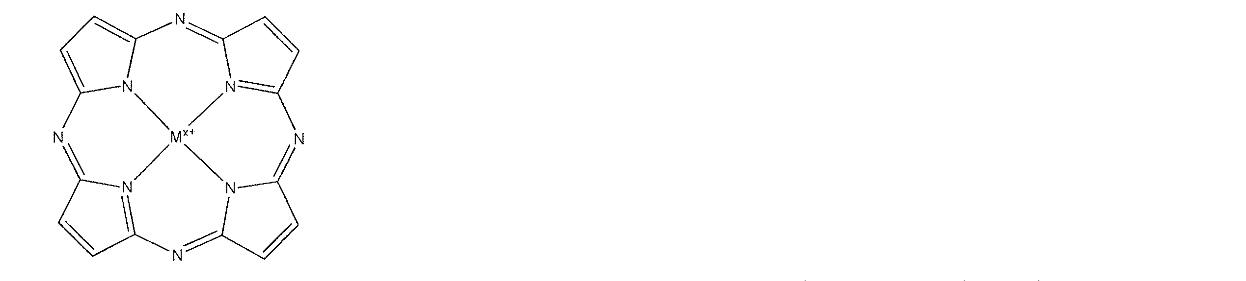
or divalent or polyvalent complexes or salts thereof, such as the following complexes:
リンカー構成成分は、単一のコアを含むことができ、また橋架けジ-イミン(例えば、4,4’-ビピリジル、1,2-ジピリジルエテン、1,4-ジピリジルテトラジン)、2つ以上のピリジル基(すなわち、ポリ-ピリジル化合物)で置換した大員環(例えば、ポルフィリンまたはフタロシアニン)を含む群から選択されてもよい。 The linker component can comprise a single core and also a bridging di-imine (eg, 4,4′-bipyridyl, 1,2-dipyridylethene, 1,4-dipyridyltetrazine), two or more (ie poly-pyridyl compounds) substituted macrocycles (eg porphyrins or phthalocyanines).
[CORE]が上記で定義したものなどの単一のコア基を含む場合、リンカー構成成分は、好適には、例えば、窒素、酸素、および/または硫黄などの1つ以上のヘテロ原子を含むものなど、電子対供与配位部分を有するQ基およびW基を含む。しかし、当業者であれば、単一のコア基はそれ自体、1つ以上の、好適には2つ以上の配位部分(例えば、窒素、酸素および/または硫黄など1つ以上のヘテロ原子を含むものなど)を含んでもよく、それら自体が電子対受容部分を含むQ基および/またはW基に接続していてもよいことが理解されるだろう。 When [CORE] comprises a single core group such as those defined above, the linker component suitably comprises one or more heteroatoms such as, for example, nitrogen, oxygen and/or sulfur. including Q and W groups with electron pair donating coordinating moieties such as . However, those skilled in the art will appreciate that a single core group may itself have one or more, preferably two or more coordinating moieties (e.g., one or more heteroatoms such as nitrogen, oxygen and/or sulfur). ), which themselves may be attached to Q and/or W groups containing electron pair accepting moieties.
好適には、各電子対供与Q基および/またはW基は、孤立電子対を担持する内部または外部ヘテロ原子を含む任意の好適な基から選択される。最も好適には、電子対供与Q基および/またはW基またはそれらのそれぞれは、任意的に置換されていてもよい、ヘテロシクリル、ヘテロアリール、ヘテロシクリル(1~6C)アルキル、ヘテロアリール(1~6C)アルキルから独立して選択されるか、または、(1~12C)アルキル、(1~12C)アルケニル、(1~12C)アルキニル、(3~8C)シクロアルキル、(3~8C)シクロアルケニル、(1~3C)アルキル(3~8C)シクロアルキル、(1~3C)アルキル(3~8C)シクロアルケニル、アリール、(1~3C)アルキルアリールもしくはアリール(1~3C)アルキルから選択され、例えば、アミノ、アルキルアミノ、ジアルキルアミノ、ヒドロキシル、(1~6C)アルコキシ、カルボニル、イミノ、チオ、チオカルボニルなどの1つ以上の塩基またはキレート基で置換されている。一実施形態では、電子供与Q基および/またはW基またはそれぞれの各電子供与Q基および/またはW基は、ピリジル、アミノフェニル、N-(1~3C)アルキルアミノフェニル、N,N-ジ(1~3C)アルキルアミノフェニル、最も好ましくはピリジル、最も好適には4-ピリジルから独立して選択される。例えば、特定の実施形態では、リンカーは以下のとおりである。
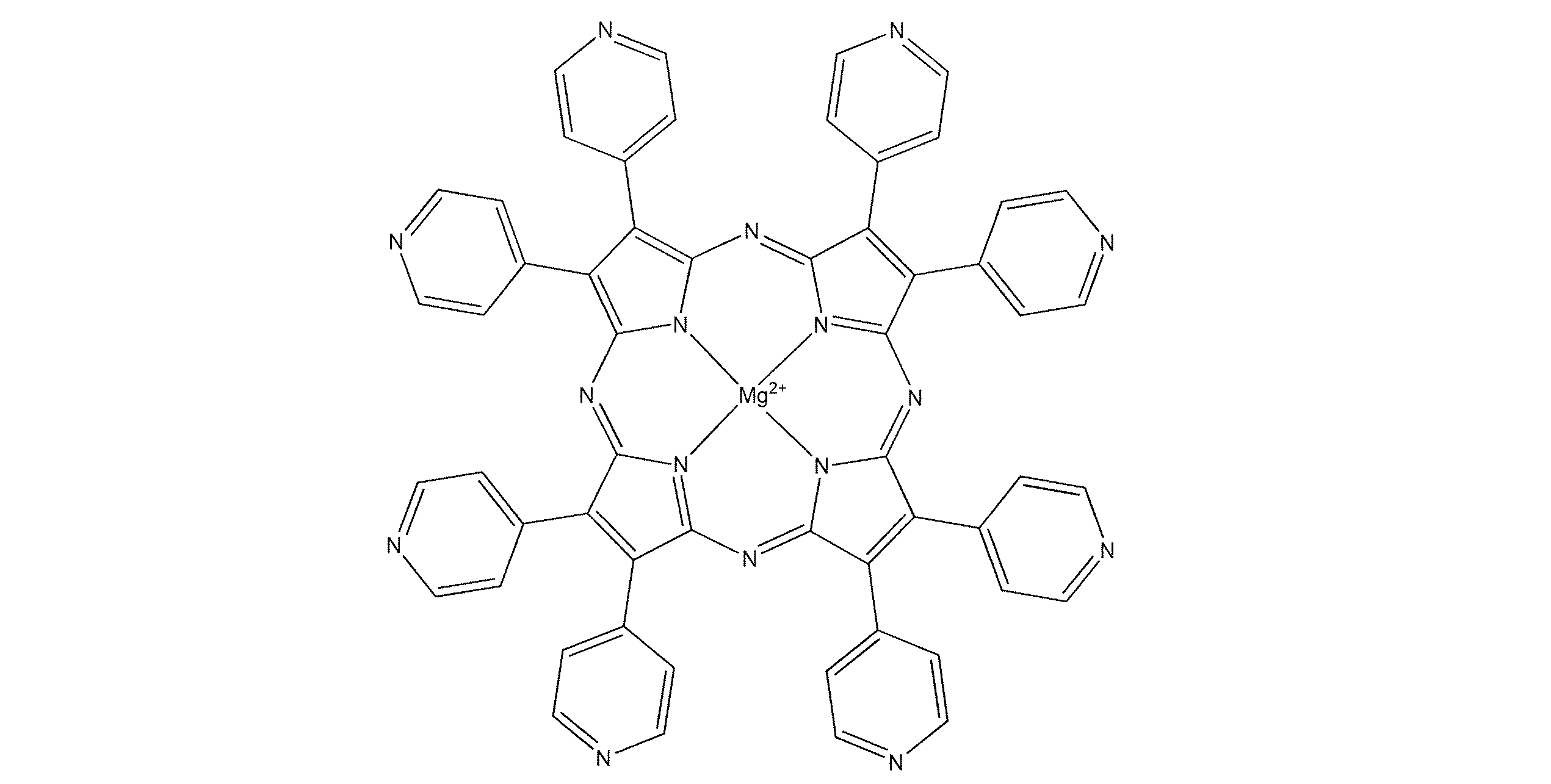
好適には、各ピリジル部分は、一次金属錯体と配位することができる。 Suitably each pyridyl moiety is capable of coordinating with a primary metal complex.
[CORE]は、Q基および/または1つ以上のW基もしくはW基(複数可)の各々を介して[CORE]を形成するために一緒に間接的に連結された複数のコア基を含むことができる。このような[CORE]は、1つ以上のQ基および/またはW基が金属中心である場合(この場合、ホウ素およびケイ素を中心とし、標準的な金属中心を含み、例えば、ルイス酸/電子対受容配位基を提供するため)に、特に重要である。このようなコア基の各々は、以下から独立して選択され得る:
a)2つ以上の孤立電子対(例えば、O2-、オキソ)を供与することができる単一の配位部分を含む単一の原子、分子、イオン、または錯体;
b)2つ以上の配位部分を含み、それぞれの配位部分が独立して孤立電子対(例えば、窒素、酸素もしくは硫黄などの内部ヘテロ原子など、または任意の置換基によって担持された外部ヘテロ原子)(例えば、カルボキシレート)を供与することができる単一の分子、イオン、または錯体(例えば、複数のヘテロ原子を含有し、任意的に置換されていてもよい、非環式、環式、多環式または大環状分子)。
[CORE] comprises multiple core groups indirectly linked together to form [CORE] via a Q group and/or one or more W groups or each of the W group(s) be able to. Such a [CORE] is where one or more of the Q and/or W groups are metallic centers (in this case boron and silicon centered, including standard metallic centers, e.g. Lewis acid/electron (to provide counter-accepting coordinating groups). Each such core group may be independently selected from:
a) a single atom, molecule, ion, or complex comprising a single coordinating moiety capable of donating two or more lone electron pairs (e.g., O 2− , oxo);
b) comprising two or more coordinating moieties, each coordinating moiety being independently a lone pair of electrons (e.g., an internal heteroatom such as nitrogen, oxygen or sulfur, or an external heteroatom carried by any substituent; a single molecule, ion, or complex (e.g., containing multiple heteroatoms and optionally substituted , acyclic , cyclic , polycyclic or macrocyclic).
例えば、各コア基は、酸素、硫黄もしくはハロ(特に、フルオロもしくはクロロ、特にフルオロ)原子、最も好適には、ハロゲン化物(好ましくはフルオロ)、オキソ、酸化物、水酸化物(OH-)、(1~6C)アルコキシド、(2~6C)アルケニルオキシ、(2~6C)アルキニルオキシ、ホルミル、カルボキシ、(1~6C)アルコキシカルボニル、(2~6C)アルカノイル、(2~6C)アルカノイルオキシ、スルホ、スルフィド、硫化水素、(1~6C)アルキルチオ、(2~6C)アルケニルチオ、(2~6C)アルキニルチオ、チオカルボニル、酸素もしくは硫黄から選択される少なくとも1つの内部ヘテロ原子、または(必要に応じて)脱プロトン化形態もしくはその塩を含むヘテロシクリルを含むか、またはそれらからなる単一の原子、分子、イオンもしくは錯体から独立して選択されてもよく、任意のCH、CH2またはCH3は、任意的に置換されている。 For example, each core group may comprise an oxygen, sulfur or halo (especially fluoro or chloro, especially fluoro) atom, most suitably a halide (preferably fluoro), oxo, oxide, hydroxide (OH—), (1-6C) alkoxide, (2-6C) alkenyloxy, (2-6C) alkynyloxy, formyl, carboxy, (1-6C) alkoxycarbonyl, (2-6C) alkanoyl, (2-6C) alkanoyloxy, at least one internal heteroatom selected from sulfo, sulfide, hydrogen sulfide, (1-6C)alkylthio, (2-6C)alkenylthio, (2-6C)alkynylthio, thiocarbonyl, oxygen or sulfur; may be independently selected from single atoms, molecules, ions or complexes comprising or consisting of heterocyclyl, including deprotonated forms or salts thereof, any CH, CH2 or CH 3 is optionally substituted .
例えば、各コア基は、酸素、窒素、硫黄もしくはハロ(特にフルオロもしくはクロロ、特にフルオロ)原子を含むかまたはそれらからなる2つ以上の配位部分を含む、単一の分子、イオン、もしくは錯体から独立して選択されてもよく、2つ以上の配位部分は、最も好適には、ハロゲン化物(好ましくはフルオロ)、アミノ、シアノ、イミノ、エナミノ、(1~6C)アルキルアミノ、ジ-[(1~6C)アルキル]アミノ、トリ-[(1~6C)アルキル]アミノ、オキソ、酸化物、水酸化物(OH-)、(1~6C)アルコキシド、(2~6C)アルケニルオキシ、(2~6C)アルキニルオキシ、ホルミル、カルボキシ、(1~6C)アルコキシカルボニル、(2~6C)アルカノイル、(2~6C)アルカノイルオキシ、スルホ、硫化物、硫化水素、(1~6C)アルキルチオ、(2~6C)アルケニルチオ、(2~6C)アルキニルチオ、チオカルボニル、窒素、酸素もしくは硫黄から選択される少なくとも1つの内部ヘテロ原子を含むヘテロシクリル、窒素、酸素または硫黄、または(必要に応じて)脱プロトン化形態もしくはその塩から選択される少なくとも1つの内部ヘテロ原子を含むヘテロアリール(例えば、ピリジル)から選択される2つ以上の基を含むかまたはそれらからなり、任意のCH、CH2またはCH3は、任意的に置換されている。 For example, each core group is a single molecule, ion, or complex containing two or more coordinating moieties comprising or consisting of oxygen, nitrogen, sulfur or halo (especially fluoro or chloro, especially fluoro) atoms. and the two or more coordinating moieties are most suitably halide (preferably fluoro), amino, cyano, imino, enamino, (1-6C)alkylamino, di- [(1-6C)alkyl]amino, tri-[(1-6C)alkyl]amino, oxo, oxide, hydroxide (OH-), (1-6C)alkoxide, (2-6C)alkenyloxy, (2-6C) alkynyloxy, formyl, carboxy, (1-6C) alkoxycarbonyl, (2-6C) alkanoyl, (2-6C) alkanoyloxy, sulfo, sulfide, hydrogen sulfide, (1-6C) alkylthio, (2-6C)alkenylthio, (2-6C)alkynylthio, thiocarbonyl, heterocyclyl containing at least one internal heteroatom selected from nitrogen, oxygen or sulfur, nitrogen, oxygen or sulfur, or (optionally ) comprising or consisting of two or more groups selected from heteroaryl (e.g. pyridyl) containing at least one internal heteroatom selected from deprotonated forms or salts thereof, optionally CH, CH2 or CH3 is optionally substituted .
特定の実施形態では、各コア基は、本明細書で定義されるbiLIG1基、本明細書で定義されるbiLIG2基、または本明細書で定義されるoptLIG1基から独立して選択されてもよい。特定の実施形態では、各コア基は、本明細書で定義されるbiLIG1基または本明細書で定義されるbiLIG2基、最も好適にはbiLIG1基から独立して選択される。最も好適には、コア基、コア基の各々、または全ては、カルボキシレートまたはカルボン酸であり、最も好適には式-O2CRB1によって定義されるかまたは式-O2CRB2(またはRB2CO2 -)によって定義されるカルボキシレートまたはカルボン酸であり、式中、RB1およびRB2は、好適には本明細書で定義されるとおりであるが、最も好適にはRB1は(1~5C)アルキルであり、RB2はピリジル、アミノフェニル、N-(1~3C)アルキルアミノフェニル、N,N-ジ(1~3C)アルキルアミノフェニルである。 In certain embodiments, each core group is independently selected from one biLIG group as defined herein, two biLIG groups as defined herein, or one optLIG group as defined herein. may In certain embodiments, each core group is independently selected from a biLIG 1 group as defined herein or a biLIG 2 group as defined herein, most preferably a biLIG 1 group. Most preferably, the core group, each or all of the core groups, is a carboxylate or carboxylic acid, most preferably defined by the formula —O 2 CR B1 or —O 2 CR B2 (or R B2 CO 2 − ), wherein R B1 and R B2 are preferably as defined herein, but most preferably R B1 is ( 1-5C)alkyl, and R B2 is pyridyl, aminophenyl, N-(1-3C)alkylaminophenyl, N,N-di(1-3C)alkylaminophenyl.
好適には、[CORE]が複数のコア基を含む場合、コア基は同じである。 Preferably, when [CORE] comprises multiple core groups, the core groups are the same.
一例として、[CORE]が複数のコア基を含むリンカーは、以下によって定義され得る:
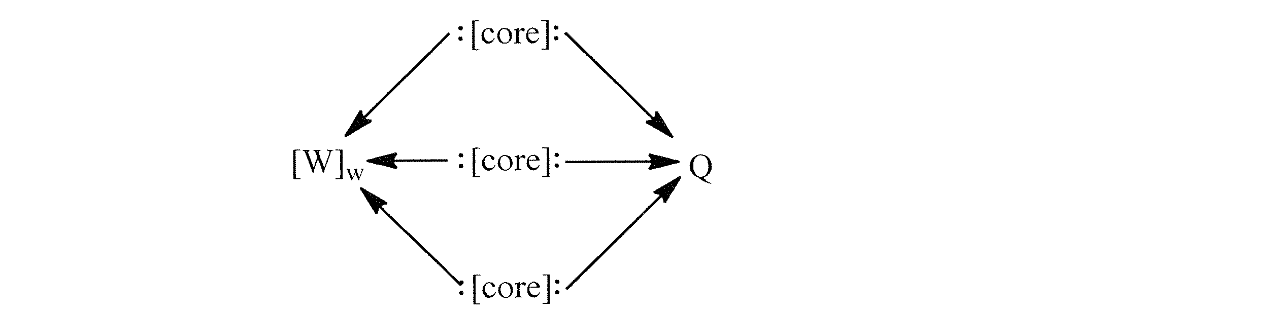
好適には、電子対受容Q基および/またはW基または各電子対受容Q基および/またはW基は、1つ以上の、好適には2つ以上の孤立電子対を受容することができる配位部分を含む単一の原子、分子、イオンまたは錯体である。好適には、関連する配位部分は、ルイス酸性金属原子(ホウ素またはケイ素を含み得る)、または脱離基もしくは置換可能な配位子に接着された金属原子を含むか、もしくはそれらからなる。例えば、配位部分は、金属カチオン(例えば、二価の金属カチオン)、ルイス酸性金属化合物(好適にはAlCl3、FeCl3、ZnCl2などのルイス酸金属化合物)、ルイス酸性金属錯体(好適には、ルイス酸または1つ以上の自由配位部位を有する錯体、例えば、金属中心がその原子価シェル中に18個未満の電子を有する錯体など)および/または脱離基もしくは置換可能な配位子を含む金属化合物もしくは錯体(好適には、脱離基もしくは置換可能な配位子の共役酸が、標準的な周囲温度および圧力にて、水中で1以下、好適には0以下、好適には-1以下、より好適には-5以下のpKaを有する)から選択される基であるか、またはこれらの基を含んでもよい。好適な金属カチオンは、二価カチオン(例えば、アルカリ土類金属、遷移金属(II)、またはSn2+カチオン)、三価カチオン(例えば、Al3+、遷移金属(III)またはf-ブロック金属(III)カチオン)、または四価カチオン(Sn4+、Pb4+、遷移金属(IV)またはf-ブロック金属(IV)カチオン)、最も好適には二価カチオンを含んでもよい。好適には、ルイス酸性金属化合物は、ホウ素化合物(例えば、ハロゲン化ホウ素、アルコキシドなど)、ケイ素化合物(例えばシラン、シリオキサン、ハロゲン化ケイ素など)、ルイス酸性金属化合物(AlCl3、FeCl3、ZnCl2など)を含んでもよい。好適なルイス酸性金属錯体または脱離基もしくは置換可能な配位子を含む錯体は、例えば二金属カルボン酸錯体(例えば、[M2(O2C-R)4]であり、MはCu2+、Ru2+、Rh2+であってもよい)、三金属カルボン酸錯体(例えば、[M2M’O(O2CR)6]であり、Mは三価の金属イオンであってもよく、M’は二価の金属イオンであってもよい)、六金属カルボン酸錯体(例えば[M’4M2O2(O2CR)12]であり、Mは、三価の金属イオンであってもよく、M’は二価の金属イオンであってもよい)、十二金属錯体(例えば、[Ni12(chp)12(O2CMe)6(H2O)6]であり、式中chp=6-クロロ-2-ピリドネート)などのカルボン酸錯体、金属中心が脱離基に結合した金属化合物(例えば塩化物、例えばAlCl3などのハロゲン化物)であり、金属中心(複数可)が、ハロゲン化物、水、THFなどの溶媒、ピリジン、またはさらにカルボキシレートなどの置換可能な配位子と配位している金属錯体、を含んでもよい。しかし、好ましい実施形態では、電子対受容Q基および/またはW基または各電子対受容Qおよび/もしくはW基は、独立して金属カチオンであり、好適には独立して、二価または三価の金属カチオンであり、好適には本明細書で定義されたとおりである。好適には、Q基は、少なくとも1つのW基と異なっていてもよい。好適には、全てのQ基およびW基は同じであってもよい。 Preferably, the electron pair accepting Q and/or W group or each electron pair accepting Q and/or W group is a coordination group capable of accepting one or more, preferably two or more lone electron pairs. A single atom, molecule, ion or complex containing a moiety. Suitably, the relevant coordinating moiety comprises or consists of a Lewis acidic metal atom (which may include boron or silicon), or a metal atom attached to a leaving group or displaceable ligand. For example, the coordinating moiety may be a metal cation (e.g., a divalent metal cation), a Lewis acidic metal compound (preferably a Lewis acid metal compound such as AlCl3 , FeCl3 , ZnCl2 ), a Lewis acidic metal complex (preferably is a Lewis acid or a complex with one or more free coordination sites, such as a complex in which the metal center has less than 18 electrons in its valence shell) and/or a leaving group or displaceable coordination A metal compound or complex containing a group (preferably a leaving group or a displaceable ligand conjugate acid is 1 or less, preferably 0 or less, preferably 0 or less, in water at normal ambient temperature and pressure) has a pKa of -1 or less, more preferably -5 or less). Suitable metal cations are divalent cations (eg alkaline earth metal, transition metal (II) or Sn 2+ cations), trivalent cations (eg Al 3+ , transition metal (III) or f-block metal (III ) cations), or tetravalent cations (Sn 4+ , Pb 4+ , transition metal (IV) or f-block metal (IV) cations), most preferably divalent cations. Suitably, the Lewis acidic metal compounds are boron compounds (e.g. boron halides, alkoxides, etc.), silicon compounds (e.g. silanes, siloxanes, silicon halides, etc.), Lewis acidic metal compounds (AlCl3 , FeCl3 , ZnCl2 etc.) may be included. Suitable Lewis acidic metal complexes or complexes containing leaving groups or displaceable ligands are, for example, bimetallic carboxylic acid complexes (eg [M 2 (O 2 C—R) 4 ], where M is Cu 2+ , Ru 2+ , Rh 2+ ), trimetallic carboxylic acid complexes (e.g., [M 2 M′O(O 2 CR) 6 ], where M can be a trivalent metal ion, M′ may be a divalent metal ion), a hexametallic carboxylic acid complex (e.g. [M′ 4 M 2 O 2 (O 2 CR) 12 ], and M is a trivalent metal ion. M′ may be a divalent metal ion), a dodecadal metal complex (e.g., [Ni 12 (chp) 12 (O 2 CMe) 6 (H 2 O) 6 ], having the formula (chp = 6-chloro-2-pyridonate), metal compounds (e.g. chlorides, e.g. halides such as AlCl 3 ) in which the metal center is attached to a leaving group, and the metal center(s) may include halides, water, solvents such as THF, pyridine, or even metal complexes coordinated with displaceable ligands such as carboxylates. However, in preferred embodiments, the electron-pair-accepting Q and/or W group or each electron-pair-accepting Q and/or W group is independently a metal cation, preferably independently a divalent or trivalent is a metal cation of, preferably as defined herein. Suitably the Q group may be different from at least one W group. Suitably all Q and W groups may be the same.
特定の実施形態では、リンカーは、以下から選択される:
-二金属カルボン酸錯体(例えば[M2(O2CR)4]であり、式中、M=Cu、Ru、Rhである)、
-三金属カルボン酸錯体(例えば[M2M’O(O2CR)6]であり、Mは三価の金属イオンであり、M’は二価の金属イオンである)、
-六金属カルボン酸錯体(例えば[M’4M2O2(O2CR)12]であり、式中、M=三価の金属イオン、M’は二価の金属イオンである)、
-[Ni12(chp)12(O2CMe)6(H2O)6](式中、chp=6-クロロ-2-ピリドネートである)などの十二金属錯体。
In certain embodiments, the linker is selected from:
- double metal carboxylic acid complexes (e.g. [M 2 (O 2 C R ) 4 ], where M = Cu, Ru, Rh),
- a trimetallic carboxylic acid complex (e.g. [M 2 M'O(O 2 CR) 6 ], where M is a trivalent metal ion and M' is a divalent metal ion),
- hexametallic carboxylic acid complexes (e.g. [M' 4 M 2 O 2 (O 2 CR) 12 ], where M = trivalent metal ion and M' is a divalent metal ion),
- twelve metal complexes such as [Ni 12 (chp) 12 (O 2 CMe) 6 (H 2 O) 6 ], where chp = 6-chloro-2-pyridonate.
リンカー構成成分(複数可)は、以下から独立して選択することができる:-本明細書で定義されるmonoLIG1基、
-本明細書で定義されるbiLIG2基、
-本明細書で定義されるoptLIG1基、
-金属錯体、
-任意に金属と配位する大環状分子、
-二金属カルボン酸錯体(例えば[M2(O2CR)4]であり、式中、M=Cu、Ru、Rhである)、
-三金属カルボン酸錯体(例えば[M2M’O(O2CR)6]であり、Mは三価の金属イオンであり、M’は二価の金属イオンである)、
-六金属カルボン酸錯体(例えば[M’4M2O2(O2CR)12]であり、式中、M=三価の金属イオン、M’は二価の金属イオンである)、
-[Ni12(chp)12(O2CMe)6(H2O)6](式中、chp=6-クロロ-2-ピリドネートである)などの十二金属錯体、
-末端配位子、例えばH2O、ピリジンまたは置換ピリジン(n=1)、
-例えば、4,4’-ビピリジル、1,2-ジピリジルエチレン、1,4-ジピリジルテトラジンなどの橋架けジ-イミン、
-ポルフィリンまたはフタロシアニンなどの大員環の周囲で置換されたピリジルなどの他のポリ-ピリジル配位子。
The linker component(s) may be independently selected from: - a monoLIG group as defined herein;
- biLIG 2 groups as defined herein,
- an optLIG group as defined herein,
- metal complexes,
- macrocycles optionally coordinated with metals,
- double metal carboxylic acid complexes (e.g. [M 2 (O 2 C R ) 4 ], where M = Cu, Ru, Rh),
- a trimetallic carboxylic acid complex (e.g. [M 2 M'O(O 2 CR) 6 ], where M is a trivalent metal ion and M' is a divalent metal ion),
- hexametallic carboxylic acid complexes (e.g. [M' 4 M 2 O 2 (O 2 CR) 12 ], where M = trivalent metal ion and M' is a divalent metal ion),
- twelve metal complexes such as [Ni 12 (chp) 12 (O 2 CMe) 6 (H 2 O) 6 ], where chp = 6-chloro-2-pyridonate;
- terminal ligands such as H 2 O, pyridine or substituted pyridine (n=1),
- bridged di-imines such as, for example, 4,4'-bipyridyl, 1,2-dipyridylethylene, 1,4-dipyridyltetrazine, etc.
- other poly-pyridyl ligands such as pyridyl substituted around macrocycles such as porphyrins or phthalocyanines.
リンカーは、これらに会合した他の溶媒和物または配位子(好適には不活性)を有するか、または塩であってもよい。 Linkers may have other solvates or ligands (preferably inert) associated with them, or may be salts.
二次電子発生剤(SEG)
本発明のレジスト組成物は、好適には、「二次電子発生剤」(SEG)を含むことができる。SEGは、好適には、レジスト組成物の他の構成成分(複数可)と比較して比較的高いZeffを有する化合物または構成成分であり、また、好適には、レジストの他の構成成分(複数可)と比較して比較的高い密度(好適には高い電子密度)を有してもよい。SEGは、好適には、照射線、特に紫外線(例えば、eUVまたはUV)への暴露時に二次電子の生成を促進する。二次電子は、一般に「横方向に」(好適には、入射ビームから80°)散乱し、これによって「書き込み」効果を広げ、レジストの感度を増大させ、また、これによって一次照射線から必要とされる「線量」を減少させる。このように、二次電子発生剤は、好適には、散乱防止剤とは反対の役割を果たす。
Secondary electron generator (SEG)
The resist compositions of the invention can suitably contain a "secondary electron generator" (SEG). The SEG is preferably a compound or component that has a relatively high Z eff compared to the other component(s) of the resist composition, and preferably the other component(s) of the resist. may have a relatively high density (preferably a high electron density) compared to the SEG preferably promotes the generation of secondary electrons upon exposure to radiation , particularly ultraviolet light (eg eUV or UV). Secondary electrons are generally "laterally" scattered (preferably at 80° from the incident beam), thereby broadening the "writing" effect, increasing the sensitivity of the resist, and thereby eliminating the need from the primary radiation . reduce the supposed “dose”. Thus, the secondary electron generator preferably plays the opposite role as the anti-scattering agent.
SEGは、レジスト組成物中の(実質的に)別個のまたは独立した構成成分(例えば、レジスト構成成分内の任意の他の構成成分、例えば散乱防止構成成分に接着されていないもの)であってもよく、または、SEGは、好適には共有結合および/または供与結合を介して、レジスト組成物の1つ以上の他の構成成分(複数可)に接着されてもよく、例えば、散乱防止化合物/構成成分に配位により接着されてもよい(SEGが金属化合物である場合特に適切であり、その対イオンまたは配位子の1つ以上が、散乱防止化合物/構成成分の供与結合部分によって置換されていてもよい)。 The SEG is a (substantially) separate or independent component in the resist composition (e.g., not adhered to any other component within the resist component, such as the anti-scatter component) Alternatively, the SEG may be attached, preferably via covalent and/or dative bonding, to one or more other component(s) of the resist composition, e.g. / may be coordinatively attached to the component (especially suitable when the SEG is a metal compound, one or more of which counterions or ligands are substituted by the dative bonding portion of the anti-scattering compound/component). may have been).
特許公開WO2015/145144(同じ発明者/出願人による)は、これらの使用の根底にある原理とともに、一連の好適な二次電子発生剤の範囲を記載している。これらのSEGのいずれも、別個の/独立した構成成分としてであろうと、または(上記のような)他の構成成分のうちの1つと接着されていても、本発明のレジスト組成物内に組み込むことができる。WO2015/145144は、参照により本明細書に組み込まれる。 Patent publication WO2015/145144 (by the same inventor/applicant) describes a range of suitable secondary electron generators along with the principles underlying their use. Any of these SEGs are incorporated into the resist composition of the present invention, whether as a separate/independent component or adhered to one of the other components (as described above). be able to. WO2015/145144 is incorporated herein by reference.
二次電子発生剤は、好適には、化合物(およびSEG化合物)または15以上の実効原子番号(Zeff)を有するこのような化合物に由来する基(例えば、SEG基は別の構成成分と供与結合していてもよい)であるか、またはこれらを含む(任意により、Zeff計算では、前述の化合物と会合する、100kPaの圧力で150℃以下の沸点を有する溶媒和物、好適には前述の圧力で120℃以下の沸点を有する任意の溶媒和物、好適には前述の圧力で105°C以下の沸点を有する任意の溶媒和物を除外する)。 The secondary electron generator is preferably a compound (and SEG compounds) or a group derived from such a compound having an effective atomic number (Z eff ) of 15 or greater (e.g., the SEG group is donated with another component). (optionally, in Zeff calculations, a solvate with a boiling point of 150° C. or less at a pressure of 100 kPa associated with the aforementioned compound, preferably the aforementioned Any solvate with a boiling point of 120° C. or less at pressure, preferably any solvate with a boiling point of 105° C. or less at the aforementioned pressures is excluded).
SEGが、SEG化合物から誘導されたSEG基(例えば、散乱防止化合物などの別の構成成分に供与結合している-HgCl基または-HgI基、)の形態である場合、好適には、Zeff(またはSEG化合物に関連して本明細書で定義される任意の他の特性および特徴)は、SEG基が誘導される初期化合物のZeff(または対応する特性もしくは特徴)を参照することによって定義され得る。しかし、代替的には、所与のSEG基のZeff(またはSEG化合物に関連して本明細書で定義される任意の他の特性および特徴)は、SEG基自体のZeff(または対応する特性または特徴)を参照することによって定義され得る(それが接着されている分子、例えば、散乱防止化合物を排除することによって計算される)。 If the SEG is in the form of a SEG group derived from a SEG compound (e.g., a -HgCl or -HgI group datively bonded to another component such as an anti-scattering compound), preferably Z eff (or any other property or characteristic defined herein in relation to an SEG compound) is defined by reference to Z eff (or the corresponding property or characteristic) of the initial compound from which the SEG group is derived can be Alternatively, however, the Z eff of a given SEG group (or any other properties and characteristics defined herein in relation to SEG compounds) is the Z eff of the SEG group itself (or the corresponding property or characteristic) (calculated by excluding the molecule to which it is attached, eg, an anti-scattering compound).
好適には、Zeffは、18以上、好適には23以上、好適には25以上、好適には30以上、好適には32以上、好適には40以上である。好適には、Zeffは、70以下、好適には66以下、好適には61以下、好適には60以下、好適には55以下である。二次電子発生剤は、好適には、散乱防止構成成分よりも高い、好適には少なくとも10単位高い、好適には少なくとも20単位高い、好適には少なくとも30単位高い、Zeffを有する。 Preferably Z eff is 18 or greater, preferably 23 or greater, preferably 25 or greater, preferably 30 or greater, preferably 32 or greater, preferably 40 or greater. Preferably Z eff is 70 or less, preferably 66 or less, preferably 61 or less, preferably 60 or less, preferably 55 or less. The secondary electron generator preferably has a Z eff higher than the anti-scattering component, preferably at least 10 units higher, preferably at least 20 units higher, preferably at least 30 units higher.
好適には、二次電子発生剤は、500g/mol以下の分子量を有する化合物または基であるかまたはそれらを含む。 Preferably, the secondary electron generator is or comprises a compound or group having a molecular weight of 500 g/mol or less.
二次電子発生剤は、好適には、金属化合物(または、例えば、別の化合物に供与結合または共有結合される場合、-HgClまたは-HgIなどの金属基)であるかまたはそれを含む。これは、元素金属(すなわち、金属(0))でなくても、またはこれを含まなくてもよい。実際、好適には、レジスト組成物は、(実質的に)任意の金属(0)を含まない。好適には、金属化合物の任意の金属種は金属イオンである。 The secondary electron generator preferably is or comprises a metal compound (or a metal group such as -HgCl or -HgI when datively or covalently bonded to another compound, for example). It may not be or contain an elemental metal (ie, metal (0)). In fact, preferably the resist composition is (substantially) free of any metal (0). Suitably any metal species of the metal compound is a metal ion.
二次電子発生剤の化合物(複数可)(またはSEG基(複数可)が誘導される化合物(複数可))は、好適には、ベースポリマー構成成分の密度よりも高い密度を有する。二次電子発生剤の化合物(複数可)は、好適には、1.7g/cm3以上、好適には2g/cm3以上、好適には2.5g/cm3以上、好適には3g/cm3、好適には4g/cm3以上、より好適には4.1g/cm3以上、好適には4.5g/cm3以上、より好適には4.7g/cm3以上、最も好適には5g/cm3以上の密度を有する。二次電子発生剤の化合物(複数可)は、好適には9g/cm3以下、好適には8.5g/cm3以下、好適には8g/cm3以下の密度を有する。特定の実施形態では、二次電子発生剤の化合物(複数可)は、好適には3.5~8.3g/cm3の密度を有する。好適には、密度は、散乱防止構成成分の密度より少なくとも2倍高く、好適には少なくとも3倍高い。
The compound(s) of the secondary electron generator (or the compound(s) from which the SEG group(s) are derivatized) preferably have a density higher than that of the base polymer constituents. The compound(s) of the secondary electron generator is preferably 1.7 g/cm 3 or more, preferably 2 g/cm 3 or more, preferably 2.5 g/cm 3 or more, preferably 3 g/
好適には、二次電子発生剤の任意の金属化合物(複数可)は、+1以上、好適には+2以上、好適には+3以上の酸化状態を有する金属種を含む。好適には、二次電子発生剤の任意の金属化合物(複数可)は、+4以下の酸化状態を有する金属種を含む。好適には、二次電子発生剤の任意の金属化合物(複数可)は、+3の酸化状態を有する金属種を含む。 Preferably, any metal compound(s) of the secondary electron generator comprises a metal species having an oxidation state of +1 or higher, preferably +2 or higher, preferably +3 or higher. Suitably, any metal compound(s) of the secondary electron generator comprises a metal species having an oxidation state of +4 or less. Suitably, any metal compound(s) of the secondary electron generator comprises a metal species having an oxidation state of +3.
好適には、二次電子発生剤の任意の金属化合物(複数可)は、単一の金属種または他の優勢な金属種(すなわち、全金属種の少なくとも50重量%、好適には少なくとも80重量%、好適には少なくとも90重量%、好適には少なくとも95重量%で構成されている金属種)を含む。二次電子発生剤のこのような金属化合物(複数可)の金属種または金属イオン(単一または優勢にかかわらず)は、好適には+1以上、好適には+2以上、好適には+3以上の酸化状態を有する。二次電子発生剤のこのような金属化合物(複数可)の金属種または金属イオン(単一または優勢にかかわらず)は、好適には+4以下の酸化状態を有する。二次電子発生剤のこのような金属化合物(複数可)の金属種または金属イオン(単一または優勢にかかわらず)は、好適には+3の酸化状態を有する。一実施形態では、二次電子発生剤のこのような金属化合物(複数可)の金属種または金属イオンは、+2の酸化状態を有する。 Preferably, any metal compound(s) of the secondary electron generator comprises a single metal species or other predominant metal species (i.e. at least 50% by weight, preferably at least 80% by weight of all metal species). %, preferably at least 90%, preferably at least 95% by weight of the metal species). The metal species or metal ions (whether singly or predominantly) of such metal compound(s) of the secondary electron generator are preferably +1 or greater, preferably +2 or greater, preferably +3 or greater. It has an oxidation state. The metal species or metal ions (whether singular or predominant) of such metal compound(s) of the secondary electron generator preferably have an oxidation state of +4 or less. The metal species or metal ions (whether singular or predominant) of such metal compound(s) of the secondary electron generator preferably have an oxidation state of +3. In one embodiment, the metal species or metal ions of such metal compound(s) of the secondary electron generator have an oxidation state of +2.
二次電子発生剤の任意の金属化合物(複数可)は、好適には、原子番号(Z)が21以上(すなわち、スカンジウムまたはそれ以降)である金属種(または単一もしくは優勢な金属種)を含む。二次電子発生剤の任意の金属化合物(複数可)は、好適には、原子番号(Z)が22以上(すなわち、チタンまたはそれ以降)の金属種(または単一もしくは優勢な金属種)を含む。二次電子発生剤の任意の金属化合物(複数可)は、好適には、原子番号(Z)が39以上(すなわち、イットリウムまたはそれ以降)である金属種(または単一もしくは優勢な金属種)を含む。二次電子発生剤の任意の金属化合物(複数可)は、好適には、原子番号(Z)が49以上(すなわち、インジウムまたはそれ以降)である金属種(または単一もしくは優勢な金属種)を含む。二次電子発生剤の任意の金属化合物(複数可)は、好適には、原子番号(Z)が57以上(すなわち、ランタンまたはそれ以降)の金属種(または単一もしくは優勢な金属種)を含む。二次電子発生剤の任意の金属化合物(複数可)は、好適には、原子番号(Z)が82以上(すなわち、鉛またはそれ以降)である金属種(または単一もしくは優勢な金属種)のみを含む。二次電子発生剤の任意の金属化合物(複数可)は、好適には、原子番号(Z)が80以上(すなわち、水銀またはそれ以降)である金属種(または単一もしくは優勢な金属種)のみを含む。金属化合物(複数可)の金属種は、好適には、d-ブロック、p-ブロックまたはf-ブロック金属種、またはこれらの混合物であり得る。好適には、金属化合物(複数可)は非照射性である。 Any metal compound(s) of the secondary electron generator is preferably a metal species (or single or predominant metal species) having an atomic number (Z) of 21 or greater (i.e., scandium or higher) including. Any metal compound(s) of the secondary electron generator preferably comprise a metal species (or single or predominant metal species) with an atomic number (Z) of 22 or greater (i.e., titanium or higher). include. Any metal compound(s) of the secondary electron generator is preferably a metal species (or single or predominant metal species) having an atomic number (Z) of 39 or greater (i.e. yttrium or higher) including. Any metal compound(s) of the secondary electron generator is preferably a metal species (or single or predominant metal species) having an atomic number (Z) of 49 or greater (i.e., indium or higher) including. Any metal compound(s) of the secondary electron generator preferably comprises a metal species (or single or predominant metal species) with an atomic number (Z) of 57 or greater (i.e., lanthanum or higher). include. Any metal compound(s) of the secondary electron generator is preferably a metal species (or single or predominant metal species) having an atomic number (Z) of 82 or greater (i.e. lead or higher) contains only Any metal compound(s) of the secondary electron generator is preferably a metal species (or single or predominant metal species) with an atomic number (Z) of 80 or greater (i.e., mercury or higher) contains only The metal species of the metal compound(s) may suitably be d-block, p-block or f-block metal species, or mixtures thereof. Suitably the metal compound(s) is non- irradiative .
好適には、二次電子発生剤は、金属ハロゲン化物またはその錯体(例えば、HAuCl4)であるか、またはそれらを含む。好適には、二次電子発生剤は、ハロゲン化金属(I)、ハロゲン化金属(II)、ハロゲン化金属(III)、もしくはハロゲン化金属(IV)、またはこれらの錯体である。好適には、二次電子発生剤は、ハロゲン化金属(III)またはハロゲン化金属(I)、またはこれらの錯体である。好適には、二次電子発生剤は、金属塩化物、好適には金属(I)塩化物、金属(II)塩化物、金属(III)塩化物または金属(IV)塩化物である。好適には、二次電子発生剤は、金属塩化物、好適には金属(I)塩化物または金属(III)塩化物である。 Preferably, the secondary electron generator is or includes a metal halide or its complex (eg HAuCl 4 ). Preferably, the secondary electron generator is a metal (I) halide, a metal (II) halide, a metal (III) halide, or a metal (IV) halide, or a complex thereof. Preferably, the secondary electron generator is a metal (III) halide or metal (I) halide, or a complex thereof. Preferably the secondary electron generator is a metal chloride, preferably a metal (I) chloride, a metal (II) chloride, a metal (III) chloride or a metal (IV) chloride. Preferably the secondary electron generator is a metal chloride, preferably a metal (I) chloride or a metal (III) chloride.
二次電子発生剤は、ハロゲン化金属(II)(例えば、HgCl2)またはその錯体(例えば、散乱防止構成成分に供与配位された場合、-HgCl)であってもよい。特定の実施形態では、二次電子発生剤は金属(II)塩化物である。 The secondary electron generator may be a metal (II) halide (eg, HgCl 2 ) or a complex thereof (eg, —HgCl when donatively coordinated to an antiscattering component). In certain embodiments, the secondary electron generator is a metal (II) chloride.
二次電子発生剤は、好適には、AlCl3、TiCl3、TiCl4、CrCl3、GaCl3、YCl3、MoCl3、AgCl、InCl3、SbCl3、HfCl3、TaCl3、WCl3、OsCl3、IrCl3、AuCl、AuCl3、HAuCl4、HgCl2、CeCl3、NdCl3、ErCl3、OsO4またはそれらの任意の好適な錯体(任意の好適な塩または塩錯体を含む)を含む群から選択されてもよい。特定の実施形態では、金属化合物は、クロロ金酸(金塩化水素酸、HAuCl4)またはその水和物(HAuCl4・4H2O)である。別の実施形態では、金属化合物は、塩化金酸ナトリウム(NaAuCl4)またはその水和物(例えばNaAuCl4・2H2O)である。特定の実施形態では、金属化合物はハロゲン化水銀(II)である。特定の実施形態では、金属化合物は二塩化水銀である。特定の実施形態では、金属化合物は二ヨウ化水銀である。 The secondary electron generator is preferably AlCl3, TiCl3 , TiCl4 , CrCl3 , GaCl3 , YCl3 , MoCl3 , AgCl, InCl3 , SbCl3 , HfCl3 , TaCl3 , WCl3 , OsCl 3 , IrCl3 , AuCl , AuCl3, HAuCl4 , HgCl2 , CeCl3 , NdCl3, ErCl3 , OsO4 or any suitable complex thereof (including any suitable salt or salt complex) may be selected from In certain embodiments, the metal compound is chloroauric acid (gold hydrochloride, HAuCl 4 ) or its hydrate (HAuCl 4 .4H 2 O). In another embodiment, the metal compound is sodium chloroaurate ( NaAuCl4 ) or a hydrate thereof ( eg, NaAuCl4.2H2O ). In certain embodiments, the metal compound is a mercury(II) halide. In certain embodiments, the metal compound is mercuric dichloride. In certain embodiments, the metal compound is mercury diiodide.
二次電子発生剤は、好適には、特に溶媒中に好適に溶解されるレジスト組成物内で、非粒子状である。二次電子発生剤は、好適には、レジスト組成物に溶解する。これにより、最終的に塗布されたレジストコーティングにおいてその均一な分布が可能になり、金属有機ナノ複合コーティングの形成が促進され得る。 The secondary electron generator is preferably non-particulate, especially within the resist composition that is preferably dissolved in a solvent. The secondary electron generator is preferably dissolved in the resist composition. This allows its uniform distribution in the final applied resist coating and may facilitate the formation of metal-organic nanocomposite coatings.
本発明の文脈において、SEGは、好適には、散乱防止化合物/構成成分によって付与される有益な特性に対する解像度に(実質的に)悪影響を及ぼすことなく、関連する暴露照射線に対するレジスト感度を高めるために組み入れられる。これは、過剰量の二次電子発生剤を使用しないことによって実現可能である。追加的にまたは代替的に、これは、好適には最終的なレジスト組成物の形成前に、二次電子発生剤をレジスト組成物の別の構成成分に慎重に接着させることによって実現可能である。このような実施形態では、二次電子発生剤は、SEG基、好適には別のレジスト構成成分(例えば、散乱防止化合物)に接着させたSEG基の形態であってもよい。 In the context of the present invention, SEG preferably enhances resist sensitivity to relevant exposure radiation without (substantially) adversely affecting resolution for the beneficial properties imparted by the anti-scattering compound/component. incorporated for This can be achieved by not using an excessive amount of secondary electron generator. Additionally or alternatively, this can be accomplished by carefully adhering the secondary electron generator to another component of the resist composition, preferably prior to formation of the final resist composition. . In such embodiments, the secondary electron generator may be in the form of an SEG group, preferably an SEG group attached to another resist component (eg, an anti-scatter compound).
特定の実施形態では、二次電子発生剤は、散乱防止化合物に接着されている。好適には、1つ以上の二次電子発生剤(複数可)は、1つ以上の散乱防止化合物に接着していてもよい。このような実施形態では、1つ以上の二次電子発生剤(複数可)は、1つ以上の散乱防止化合物に、好適には1つ以上の散乱防止化合物(複数可)に会合させた1つ以上の配位子を介して、好適には共有結合または供与結合される。好適には、「未加工」散乱防止化合物(すなわち、SEG基(複数可)が接着していない)は、二次電子発生化合物と反応させるか、または他の方法で混合させて、散乱防止化合物を二次電子発生剤と会合させるか、または二次電子発生剤に接着させる。従って、得られた二次電子発生剤は、元のSEG化合物から誘導されたSEG基であってもよい。このような反応は、散乱防止化合物内の配位基または結合基による初期の二次電子発生化合物の1つ以上の基、対イオン、または配位子の置換を含み得る。あるいは、二次電子発生化合物は未処置のままであってよく、また、いかなる置換も伴わずに散乱防止化合物と供与結合を形成し得る。例えば、二次電子化合物がルイス酸として作用してもよい。 In certain embodiments, the secondary electron generator is adhered to an anti-scatter compound. Suitably, one or more secondary electron generator(s) may be adhered to one or more anti-scattering compounds. In such embodiments, one or more secondary electron generator(s) are associated with one or more antiscattering compounds, preferably one or more antiscattering compound(s). It is preferably covalently or datively linked via one or more ligands. Preferably, the "raw" anti-scattering compound (i.e., without the SEG group(s) attached) is reacted or otherwise mixed with the secondary electron generating compound to form an anti-scattering compound. is associated with or adhered to the secondary electron generator. The resulting secondary electron generator may therefore be a SEG group derived from the original SEG compound. Such reactions may involve replacement of one or more groups, counterions, or ligands of the initial secondary electron generating compound by a coordinating group or linking group within the antiscatter compound. Alternatively, the secondary electron generating compound may remain untreated and form a dative bond with the antiscattering compound without any substitution. For example, a secondary electron compound may act as a Lewis acid.
一例として、遊離孤立電子対を担持する1つ以上の配位子(アミン、イミン、ピリジンなど、例えば、ニコチン酸など)を含む散乱防止化合物(またはその前駆体)、好適には多金属ケージ型散乱防止化合物を二次電子発生化合物、例えば二ハロゲン化水銀(II)と反応させて、二次電子発生化合物またはそれらから誘導された二次電子発生剤基(例えば、対応する水銀(II)モノハライド基(-HgX))に共有結合または供与結合により結合した散乱防止化合物を含む散乱防止-SEG錯体を生成してもよい。 As an example, an anti-scattering compound (or precursor thereof), preferably of the multimetal cage type, comprising one or more ligands (amines, imines, pyridines, etc., e.g., nicotinic acid, etc.) bearing a free lone pair of electrons The anti-scattering compound is reacted with a secondary electron generating compound, such as a mercury(II) dihalide, to form a secondary electron generating compound or a secondary electron generating group derived therefrom, such as the corresponding mercury(II) mono An anti-scattering-SEG complex may be formed comprising an anti-scattering compound covalently or datively bound to a halide group (--HgX)).
特定の実施形態では、この散乱防止化合物は、好適には、本明細書で定義され、1つ以上の孤立電子対(複数可)を担持する1つ以上の配位子(好適には、アミン、イミン、ピリジン、アミドなどの孤立電子対を担持する窒素中心)を含む多金属ケージであり、(好適には、ルイス酸であるか、または置換可能な対イオン、配位子、もしくは基を含むかのいずれかである化合物から誘導される)二次電子発生剤基は、前述の孤立電子対(複数可)を介して散乱防止化合物に供与結合されている。代替的実施形態では、二次電子発生剤基は、反対の方法で、散乱防止化合物に接着されてもよい。例えば、二次電子発生化合物が、散乱防止化合物の金属中心と配位結合を形成する1つ以上の孤立電子対(複数可)を担持する1つ以上の配位子を含む。 In certain embodiments, the anti-scattering compound preferably comprises one or more ligands (preferably amine , imines, pyridines, amides, etc.) and (preferably Lewis acids or with displaceable counterions, ligands or groups A secondary electron generator group (derived from a compound that either contains or is derived from) is datively bonded to the antiscattering compound via the aforementioned lone pair(s) of electrons. In an alternative embodiment, the secondary electron generator group may be attached to the antiscatter compound in the opposite manner. For example, the secondary electron generating compound includes one or more ligands carrying one or more lone pair(s) that form coordinate bonds with the metal center of the antiscatter compound.
特定の実施形態では、散乱防止化合物は、散乱防止化合物の1分子当たり1つ以上のニコチン酸配位子を含む多金属ケージであり、1つ以上のハロゲン化水銀(II)二次電子基(好適には水銀モノハライド)は、それぞれ、ニコチン酸配位子のピリジル部分に供与結合される。 In certain embodiments, the anti-scattering compound is a polymetallic cage comprising one or more nicotinic acid ligands per molecule of the anti-scattering compound, and one or more mercury (II) halide secondary electron groups ( Mercury monohalides, preferably mercury monohalides, are each datively bonded to the pyridyl moiety of the nicotinic acid ligand.
二次電子発生剤(複数可)を散乱防止化合物に化学的に結合させることは(例えば、共有結合または供与結合を介して)、電子密度の高い散発的な(かつ好適には規則的にきちんと定義された)領域を導入し、局所的散乱を促進してレジスト感度を増大させ、高解像度のリソグラフィを促進する一般的に低濃度のレジスト組成物を有するという利点を損なうことがないことから、特に有益である。 Chemically bonding the secondary electron generator(s) to the anti-scattering compound (e.g., via covalent or dative bonding) provides an electron-dense, sporadic (and preferably regularly ordered) without compromising the advantages of having a generally low concentration resist composition that introduces a defined region, promotes localized scattering to increase resist sensitivity, and promotes high resolution lithography; particularly beneficial.
感光性構成成分
レジスト組成物/コーティングは、光開始剤、光酸または光増感剤などの感光性構成成分、好適にはレジスト組成物のレジスト構成成分(複数可)の変換の反応性を促進する構成成分を含むことができる。
Photosensitive Component The resist composition/coating promotes reactivity of conversion of a photosensitive component, such as a photoinitiator, photoacid or photosensitizer, preferably the resist component(s) of the resist composition. It can contain components that
いくつかの実施形態では、レジスト構成成分は、感光性構成成分であり得るか、そうでなければ、感光性構成成分を含有するかまたは含んでもよい。例えば、いくつかのレジスト構成成分(例えば、追加の光開始剤、光触媒などの補助なく光分解反応を受けることができるもの)は、それ自体で光分解反応性であってもよい(ただし、これは、照射線源の関連する入射波長にも依存し得る)。したがって、レジスト組成物は、好適には、光酸または光開始剤を(実質的に)含まなくてもよい。 In some embodiments, the resist component can be, or otherwise contain or include, a photosensitive component. For example, some resist components (e.g., those capable of undergoing photolytic reactions without the aid of additional photoinitiators, photocatalysts, etc.) may themselves be photolytically reactive (although this may also depend on the relevant incident wavelength of the radiation source). Accordingly, the resist composition may preferably be (substantially) free of photoacids or photoinitiators.
しかし、感光性構成成分は、別個の光開始剤または光電子生成剤であってもよい。こうした光開始剤は、吸収された光エネルギー、UVまたは可視光を開始種、すなわちフリーラジカルまたはカチオンの形態の化学エネルギーに変換する化合物であってもよい。開始ラジカルが形成されるメカニズムに基づいて、光開始剤は一般に2つのクラスに分類される:
タイプI:照射時に単分子結合開裂を受けてフリーラジカルを生じる光開始剤、
タイプII:光開始剤の励起状態が第2の分子(共開始剤)と相互作用してフリーラジカルを生成する2分子反応を受ける光開始剤。
However, the photosensitive component may also be a separate photoinitiator or photogenerator. Such photoinitiators may be compounds that convert absorbed light energy, UV or visible light, into chemical energy in the form of initiating species, ie free radicals or cations. Based on the mechanism by which the initiating radical is formed, photoinitiators are generally divided into two classes:
Type I: photoinitiators that undergo unimolecular bond cleavage upon irradiation to generate free radicals;
Type II: A photoinitiator that undergoes a bimolecular reaction in which the excited state of the photoinitiator interacts with a second molecule (co-initiator) to generate free radicals.
本発明のレジスト組成物/コーティング内での使用に好適な感光性構成成分(複数可)としては、
アセトフェノン、アントラキノン、アントラキノン-2-スルホン酸、ナトリウム塩一水和物、ベンジル、ベンゾイン、ベンゾインエチルエーテル、ベンゾインイソブチルエーテル、ベンゾインメチルエーテル、ベンゾフェノン、ベンゾフェノン/1-ヒドロキシシクロヘキシルフェニルケトン、ベンゾフェノンテトラカルボン酸二無水物、4-ベンゾイルビフェニル、カンファーキノン、2-クロロチオキサンテン、(クメン)シクロペンタジエニル鉄(II)ヘキサフルオロホスフェート、2,2-ジエトキシアセトフェノン、2,2-ジメトキシ-2-フェニルアセトフェノン、4-(ジメチルアミノ)ベンゾフェノン、2,5-ジメチルベンゾフェノン、4-エトキシアセトフェノン、フェロセン、4-ヒドロキシアセトフェノン、3-ヒドロキシアセトフェノン、2-メチルベンゾフェノン、3-メチルベンゾフェノン、メチルベンゾイルホルメート(Methybenzoylformate)、2-メチル-4’-(メチルチオ)-2-モルホリノプロピオフェノン、フェナントレンキノン、4’-フェノキシアセトフェノン、チオキサンテン-9-オン、トリアリールスルホニウムヘキサフルオロアンチモネート塩、トリアリールスルホニウムヘキサフルオロホスフェート塩を挙げることができる。
Photosensitive component(s) suitable for use in the resist compositions/coatings of the invention include:
Acetophenone, anthraquinone, anthraquinone-2-sulfonic acid, sodium salt monohydrate, benzyl, benzoin, benzoin ethyl ether, benzoin isobutyl ether, benzoin methyl ether, benzophenone, benzophenone/1-hydroxycyclohexylphenyl ketone, benzophenone tetracarboxylic acid di Anhydride, 4-benzoylbiphenyl, camphorquinone, 2-chlorothioxanthene, (cumene)cyclopentadienyl iron (II) hexafluorophosphate, 2,2-diethoxyacetophenone, 2,2-dimethoxy-2-phenylacetophenone , 4-(dimethylamino)benzophenone, 2,5-dimethylbenzophenone, 4-ethoxyacetophenone, ferrocene, 4-hydroxyacetophenone, 3-hydroxyacetophenone, 2-methylbenzophenone, 3-methylbenzophenone, methylbenzoylformate , 2-methyl-4′-(methylthio)-2-morpholinopropiophenone, phenanthrenequinone, 4′-phenoxyacetophenone, thioxanthene-9-one, triarylsulfonium hexafluoroantimonate salt, triarylsulfonium hexafluorophosphate Mention may be made of salt.
特定の実施形態では、感光性構成成分は、2,2-ジエトキシアセトフェノンおよびトリス(4-tert-ブチルフェニル)スルホニウムトリフラートからなる群から選択される。 In certain embodiments, the photosensitive component is selected from the group consisting of 2,2-diethoxyacetophenone and tris(4-tert-butylphenyl)sulfonium triflate.
本発明のレジスト構成成分内での感光性構成成分の使用の決定は、例えば、入射波長、要求される感度、要求される解像度、関連するレジスト構成成分の固有の光分解反応性などのいくつかの要因に依存し得る。 The determination of the use of photosensitive components within the resist components of the invention depends on several factors such as, for example, the incident wavelength, the sensitivity required, the resolution required, the intrinsic photolytic reactivity of the resist components involved, and the like. can depend on factors such as
特定の実施形態では、レジスト組成物は、(実質的に)任意の追加の感光性構成成分(複数可)を含有しない(レジスト構成成分(複数可)の任意の固有の感光性にかかわらず(これが好適に望ましい))か、またはレジスト組成物は、散乱防止構成成分(複数可)とレジスト構成成分(複数可)との合計重量100重量部(pbw)当たり、1pbw以下の追加の感光性構成成分(複数可)、好適には、散乱防止構成成分(複数可)とレジスト構成成分(複数可)との合計重量500pbw当たり、1pbw以下の追加の感光性構成成分(複数可)、好適には、散乱防止構成成分(複数可)とレジスト構成成分(複数可)との合計重量1000pbw当たり、1pbw以下の追加の感光性構成成分(複数可)を含む。 In certain embodiments, the resist composition does not (substantially) contain any additional photosensitive component(s) (regardless of any inherent photosensitivity of the resist component(s) ( or the resist composition contains no more than 1 pbw of additional photosensitive component per 100 parts by weight (pbw) combined weight of antiscatter component(s) and resist component(s). per 500 pbw combined weight of component(s), preferably anti-scatter component(s) and resist component(s), no more than 1 pbw additional photosensitive component(s), preferably , containing no more than 1 pbw of additional photosensitive component(s) per 1000 pbw combined weight of antiscatter component(s) and resist component(s).
レジスト架橋剤
レジスト組成物は、好適には、レジスト架橋剤をさらに含むことができ、これは、好適には、レジスト構成成分に反応し(例えば、暴露中または暴露後処理中に)、レジスト構成成分間またはレジスト構成成分と別の構成成分との間の架橋を促進する架橋構成成分である。レジスト構成成分が別のレジスト構成成分と反応することができると言われる場合、このような反応は間接的であってもよく、かつ介在するレジスト架橋剤を含んでもよい。好適な架橋剤は当該技術分野において公知である。
Resist Crosslinker The resist composition may suitably further comprise a resist crosslinker, which preferably reacts with resist constituents (e.g., during exposure or during post- exposure processing) to form a resist composition. A cross-linking component that promotes cross-linking between components or between a resist component and another component. Where a resist component is said to be capable of reacting with another resist component, such reaction may be indirect and may involve an intervening resist crosslinker. Suitable cross-linking agents are known in the art.
架橋剤は、好適には、照射線暴露後の現像液不溶性レジストの形成を促進する。 The cross-linking agent preferably facilitates the formation of a developer-insoluble resist after exposure to radiation .
任意の好適な架橋剤を使用することができるが、架橋剤は、照射源およびレジスト組成物およびその構成成分との最大の相溶性のために慎重に選択されるのが最も有利である。 Any suitable cross-linking agent can be used, but most advantageously the cross-linking agent is carefully selected for maximum compatibility with the radiation source and the resist composition and its constituents.
いくつかの実施形態では、架橋剤は、ジペンタエリスリオール(erythriol)ペンタアクリレート(DPEPA)もしくはペンタエリスリトールテトラアクリレート(PET)、または任意の他の好適な混和性多官能性アクリレートおよび/もしくはその混合物である。他の架橋剤はエポキシ(SU8)が挙げられるか、または使用されるコポリマーが例えばポリヒドロキシスチレンである場合、溶解性の変化をもたらすために好適な光酸発生剤を使用することができる。 In some embodiments, the crosslinker is dipentaerythriol pentaacrylate (DPEPA) or pentaerythritol tetraacrylate (PET), or any other suitable miscible multifunctional acrylates and/or mixtures thereof. is. Other cross-linking agents include epoxies (SU8), or if the copolymer used is, for example, polyhydroxystyrene, a suitable photoacid generator can be used to effect a change in solubility.
プラズモン構成成分
レジスト組成物/コーティングはプラズモン構成成分を含んでもよい。プラズモン構成成分は、好適には、本発明のレジスト組成物でコーティングされた表面上の表面プラズモン共鳴(SPR)効果を生じさせる構成成分または材料である。これらのプラズモン共鳴効果は、表面プラズモンが非常に低い波長を有し、入射照射線を非常に小さい次元に閉じ込める能力を継承することができるため、高解像度のリソグラフィを容易にすることができる。これについては、文献に報告されているとおりである(例えば、Lewis Sら「High density self assembled nanoparticle film with temperature-controllable interparticle spacing for deep sub-wavelength nanolithography using localized surface Plasmon modes on planar silver nanoparticle tunable grating」Microelectronic Engineering 85(2008年)486-491)。
Plasmonic Component The resist composition/coating may include a plasmonic component. A plasmonic component is preferably a component or material that produces a surface plasmon resonance (SPR) effect on a surface coated with the resist composition of the invention. These plasmon resonance effects can facilitate high-resolution lithography because surface plasmons have very low wavelengths and can inherit the ability to confine incident radiation to very small dimensions.これについては、文献に報告されているとおりである(例えば、Lewis Sら「High density self assembled nanoparticle film with temperature-controllable interparticle spacing for deep sub-wavelength nanolithography using localized surface Plasmon modes on planar silver nanoparticle tunable grating」 Microelectronic Engineering 85 (2008) 486-491).
表面プラズモン共鳴は、誘電率の異なる(典型的には負および正の誘電率材料)材料間の界面に位置する伝導帯電子の照射線刺激(例えば、UVまたは光)共鳴振動を含む当該技術分野において周知の現象である。共鳴は、正の核の復元力に抗して振動する表面電子の固有振動数に周波数が一致する光子によって誘発される。 Surface plasmon resonance involves radiation -stimulated (e.g., UV or light) resonant oscillations of conduction band electrons located at interfaces between materials with different dielectric constants (typically negative and positive dielectric constant materials). is a well-known phenomenon in Resonance is induced by photons whose frequency matches the natural frequency of surface electrons vibrating against a positive nuclear restoring force.
このように、プラズモン構成成分は、前述のSPR効果をもたらす構成成分である。好適には、プラズモン構成成分は、微粒子、好適にはナノ粒子である。したがって、レジスト組成物は、こうしたプラズモン構成成分のコロイド分散液または懸濁液であってもよい。したがって、得られるコーティングは、好適には、ナノ粒子プラズモン構成成分の薄い層(すなわち、ナノ粒子フィルム)を含む。 Thus, the plasmonic component is the component that provides the aforementioned SPR effect. Preferably, the plasmonic components are microparticles, preferably nanoparticles. Accordingly, the resist composition may be a colloidal dispersion or suspension of such plasmonic components. The resulting coating thus preferably comprises a thin layer of nanoparticle plasmonic constituents (ie, a nanoparticle film).
いくつかの実施形態では、レジスト組成物自体がプラズモン構成成分を含まなくてもよいが、その代わりにプラズモン構成成分は、関連する基板表面(別個のプラズモンコーティング組成物の一部として)上に、好ましくはそのプレレジストコーティング表面上に別個にコーティングされてもよい。リソグラフィの解像度をさらに改善するために、必要に応じて複数のプラズモンコーティングを施してもよい。 In some embodiments, the resist composition itself may not contain the plasmonic component, but instead the plasmonic component is applied onto the relevant substrate surface (as part of a separate plasmonic coating composition) by It may preferably be coated separately on the pre-resist coating surface. Multiple plasmonic coatings may be applied if desired to further improve lithographic resolution.
任意の好適なプラズモン構成成分を使用することができる。最も好適には、プラズモン構成成分は、金属ナノ粒子、例えば銀または金ナノ粒子を含む。 Any suitable plasmonic component can be used. Most preferably, the plasmonic component comprises metal nanoparticles, such as silver or gold nanoparticles.
特定の実施形態
特定の実施形態では、レジスト組成物は、二次電子発生剤に共有結合または供与結合により結合された散乱防止化合物を含み、散乱防止化合物は、好適には、二次電子発生剤と供与結合を形成する1つ以上の孤立電子対を担持する配位子と会合した多金属ケージであり、二次電子発生剤は、金属化合物、金属含有基もしくは断片、または25以上のZeffを有する金属種である。
Certain Embodiments In certain embodiments, the resist composition comprises an antiscattering compound covalently or datively bound to a secondary electron generator, the antiscattering compound preferably being a secondary electron generator. is a polymetallic cage associated with ligands carrying one or more lone pairs of electrons that form dative bonds with the secondary electron generator, the secondary electron generator being a metal compound, a metal-containing group or fragment, or a Z eff of 25 or greater is a metal species having
特定の実施形態では、レジスト組成物は、散乱防止-二次電子発生ハイブリッド化合物(または錯体)(AS-SEGハイブリッド)を含み、AS-SEGは、
-1つ以上の金属種(好適には少なくとも2つの金属種、最も好適なクロムおよびニッケル)ならびに会合配位子のセットを含む多金属ケージであって、配位子の少なくとも1つは、供与孤立電子対を含み、かつ配位子のうちの少なくとも1つは、隣接する多金属ケージと架橋を形成することが可能なπ系またはπ結合を含む、多金属ケージと、
-多金属ケージの配位子のうちの1つによって担持された供与孤立電子対を介して多金属ケージに結合された二次電子発生基であって、金属中心(好適には、多金属ケージ内の任意のものとは異なり、好適には、より高い原子数を有する金属)化合物または基を含み、好適にはハロゲン化金属を含む、二次電子発生基と、を含む。
In certain embodiments, the resist composition comprises an anti-scattering-secondary electron generating hybrid compound (or complex) (AS-SEG hybrid), wherein AS-SEG is
- a polymetallic cage comprising one or more metal species (preferably at least two metal species, most preferably chromium and nickel) and a set of associated ligands, at least one of which is a donor a multimetallic cage comprising a lone pair of electrons and at least one of the ligands comprising a π-system or π-bond capable of forming a bridge with an adjacent multimetallic cage;
- a secondary electron generating group attached to the multimetallic cage via a donating lone pair carried by one of the ligands of the multimetallic cage, wherein the metal center (preferably the multimetallic cage and secondary electron generating groups, preferably comprising metal) compounds or groups having a higher atomic number, and preferably comprising metal halides, unlike any of the above.
本発明のレジスト組成物を用いたリソグラフィ
本発明は、リソグラフィを実施する方法を提供し、この方法は、
i)本明細書で定義されるレジストコーティング基板を提供するステップ、または基板にレジストコーティングを塗布するステップと、
ii)レジストコーティングの一部分(複数可)を照射線に暴露させて、暴露されたレジストコーティングをもたらすステップと、
iii)上記暴露されたレジストコーティングを現像してレジストパターン層を生成するステップであって、上記レジストパターン層は、上記レジストコーティングの現像液不溶性コーティング部分(すなわち隆起)と上記レジストパターン層を通って延在する溝の列と、を含む、ステップと、
iv)上記レジストパターン層の下にある上記基板、基板表面またはその一部分(複数可)を改変する任意的ステップと、
v)任意により、レジストパターン層を除去して改変された基板を提供するステップと、
vi)上記改変された基板において、ステップiv)および/またはステップi)~v)を任意的に1回以上繰り返すこと(任意により、上記レジストコーティングの代わりに標準的なフォトレジストなどの代替的レジストコーティングを用いて、および任意により、暴露中に代替照射線を使用すること)と、を含み、
この方法のステップ(i)より前に、レジストコーティングまたは代替的レジストコーティングのいずれかを用いて、および暴露中に電磁波照射線または代替照射線のいずれかを用いて、ステップ(i)~(vi)(すなわち、前工程(i)~(vi))を実施することが、任意により1回以上繰り返され、
上記レジストコーティングは、本明細書で定義される、任意的に、乾燥および/または硬化されたレジスト組成物を含む。
Lithography Using Resist Compositions of the Invention The invention provides a method of performing lithography, the method comprising:
i) providing a resist-coated substrate as defined herein or applying a resist coating to the substrate;
ii) exposing a portion(s) of the resist coating to radiation resulting in an exposed resist coating;
iii) developing said exposed resist coating to produce a patterned resist layer, said patterned resist layer passing through developer insoluble coating portions (i.e. ridges) of said resist coating and said patterned resist layer; a step including an extending row of grooves;
iv) optionally modifying the substrate, substrate surface or portion(s) thereof underlying the resist pattern layer;
v) optionally removing the resist pattern layer to provide a modified substrate;
vi) optionally repeating step iv) and/or steps i)-v) one or more times on said modified substrate (optionally replacing said resist coating with an alternative resist such as standard photoresist); with a coating and optionally using alternative radiation during exposure );
Prior to step (i) of the method, with either a resist coating or an alternative resist coating, and with either electromagnetic radiation or alternative radiation during exposure , steps (i)-( vi) (i.e., performing the preceding steps (i)-(vi)) is optionally repeated one or more times,
The resist coating comprises an optionally dried and/or cured resist composition as defined herein.
好適には、この方法は、少なくとも1回のフォトリソグラフィサイクル、好適には本発明のレジストコーティングを伴う。好適には、こうしたフォトリソグラフィは、本発明の方法によって生成されたフォトマスクであるか、または標準的なフォトマスクであるか、フォトマスクを使用して実施することができる。 Preferably, the method involves at least one photolithographic cycle, preferably a resist coating of the invention. Preferably, such photolithography can be performed using a photomask, either a photomask produced by the method of the present invention or a standard photomask.
この方法のステップ(i)は、レジストコーティングまたは代替的レジストコーティングのいずれかを用いて、および暴露中に電磁波照射線または代替照射線のいずれかを用いて、任意により、ステップ(i)~(vi)を実施すること先に行って(すなわち、前工程(i)~(vi))、任意により1回以上繰り返される。 Step (i) of the method comprises using either a resist coating or an alternative resist coating and using either electromagnetic radiation or alternative radiation during exposure , optionally steps (i) to Performing (vi) is preceded (ie, preceding steps (i)-(vi)) and optionally repeated one or more times.
レジストコーティングは、好適には、本明細書で定義される任意により乾燥されたおよび/または硬化されたレジスト組成物を含むかまたは本質的にそれからなる。しかし、レジストコーティングは、1つ以上のコーティング層を含むことができ、そのうちの少なくとも1つの層が本発明のレジストコーティングである。一実施形態では、レジストコーティングは、その上に1つ以上の追加のコーティング(例えば、プラズモンコーティング)を含み得る。 The resist coating preferably comprises or consists essentially of an optionally dried and/or cured resist composition as defined herein. However, the resist coating can comprise one or more coating layers, at least one of which is the resist coating of the present invention. In one embodiment, the resist coating may include one or more additional coatings (eg, plasmonic coatings) thereon.
本発明はさらに、この方法によって得ることができるか、この方法によって得られるか、またはこの方法によって直接得られるイメージングされた基板を提供する。 The invention further provides an imaged substrate obtainable by this method, obtained by this method or obtained directly by this method.
このような方法は、イメージングのために、パターン形成された基板を調製するため、基板の表面を選択的に改変するために、および多層基板(例えば、集積回路)を製造するために、好適には本明細書で定義されているとおり使用されてもよい。 Such methods are suitable for imaging, for preparing patterned substrates, for selectively modifying the surface of substrates, and for fabricating multilayer substrates (e.g., integrated circuits). may be used as defined herein.
特定の実施形態では、上記の方法は、集積回路(多層基板の一例である)または複数の集積回路(例えば、ウェハ上の)の製造に使用される。当業者は、集積回路の製造に使用される標準的な製造プロセスを十分に認識している。本発明の方法は、集積回路の1つ以上の層を生成するために使用され、いくつかの実施形態では、全ての層を生成するために使用されてもよい。しかし、1つまたはいくつかの解像度限界層にのみ高解像度が必要とされることがあるので(例えば、解像度が全ての層にとって重要ではない場合)、他の層の製造に代替的リソグラフィ方法(例えば、標準的フォトリソグラフィ)を伴うことがある。このようにして、本発明のリソグラフィ方法は、集積回路の組み立てにおけるリソグラフィの他の形態(例えば、既存のフォトリソグラフィ技術)を補完することができる。 In certain embodiments, the methods described above are used in the fabrication of an integrated circuit (which is an example of a multi-layer substrate) or multiple integrated circuits (eg, on a wafer). Those skilled in the art are well aware of the standard manufacturing processes used in manufacturing integrated circuits. The methods of the present invention are used to produce one or more layers of an integrated circuit, and in some embodiments may be used to produce all layers. However, since high resolution may only be required for one or a few resolution-limited layers (e.g., if resolution is not critical for all layers), alternative lithographic methods (such as for example, standard photolithography). In this way, the lithographic methods of the present invention can complement other forms of lithography (eg, existing photolithographic techniques) in the fabrication of integrated circuits.
基板
リソグラフィが実施される基板は、任意の好適な基板であってもよい。
Substrate The substrate on which lithography is performed may be any suitable substrate.
基板は、好適には、単一の固体またはその一部である。基板は、好適には、(実質的に剛性の)プレート、ウェハ、またはシート、最も好適にはウェハの形態である。 The substrate is preferably a single solid body or part thereof. The substrate is preferably in the form of a (substantially rigid) plate, wafer or sheet, most preferably a wafer.
本発明の方法によれば、特定の処理ステップは、(例えば、「基板」を指すステップを含む)「繰り返す」ことができるので、「基板」は、最初の「投入基板」(すなわち、本発明の任意の方法ステップが実施される前に)または「改変された基板」(特定の方法ステップの後)を指すことができる。このように、原理的には、「基板」は、リソグラフィによる処理に好適な任意の基板(部分的に作られた製品または集積回路など)であってもよい。 According to the method of the present invention, certain processing steps can be "repeated" (including, for example, referring to a "substrate"), so that the "substrate" is the initial "input substrate" (i.e. before any method steps are performed) or "modified substrate" (after a particular method step). Thus, in principle, a "substrate" may be any substrate (such as a partially fabricated product or an integrated circuit) suitable for processing by lithography.
基板(投入基板または改変された基板のいずれか)は、好適には、予め形成されたレジストコーティング基板の一部分であるか、または本明細書で開示される多くの方法(例えば、ステップi)のレジストコーティングが塗布される基板である。このように、基板は、レジストコーティング自体に言及することなく(その性質、パラメータ、材料の形態などに関して)定義されてもよい。基板または改変された基板は、レジストコーティングでコーティングする前に平坦化されてもよい。 The substrate (either the input substrate or the modified substrate) is preferably part of a pre-formed resist-coated substrate or the A substrate to which the resist coating is applied. Thus, the substrate may be defined (in terms of its properties, parameters, material morphology, etc.) without referring to the resist coating itself. The substrate or modified substrate may be planarized prior to coating with the resist coating.
いくつかの実施形態では、本発明の方法(複数可)が適用される基板(またはその一部分)は、最終(印刷された)製品(例えば、集積回路)に組み込まれるが、それ自体が製品(例えば、集積回路および/または電子デバイス)に組み込まれてもよい。換言すれば、「イメージングされた基材」は、消耗品であるか、もしくは消耗品になるか、または消耗品に組み込まれるか、もしくは組み込まれるようになる可能性がある。このような消耗品には、集積回路、集積回路ダイもしくはウェハ、集積回路パッケージ、回路基板、または電子デバイスもしくはシステムが含まれる。 In some embodiments, the substrate (or portion thereof) to which the method(s) of the invention is applied is incorporated into a final (printed) product (e.g., an integrated circuit), but itself is a product ( integrated circuits and/or electronic devices). In other words, the "imaged substrate" is or becomes a consumable, or is or can become incorporated into a consumable. Such consumables include integrated circuits, integrated circuit dies or wafers, integrated circuit packages, circuit boards, or electronic devices or systems.
しかし、いくつかの実施形態では、本発明の方法(複数可)が適用される基板(またはその一部分)は、最終(印刷された)製品(例えば、集積回路)には組み込まれず、むしろ、例えば、このような最終(印刷された)製品を製造するために使用されるフォトリソグラフィに使用するためのフォトマスクなどのリソグラフィマスク(ポジティブまたはネガティブのいずれでもよい)などのツールに組み込まれる。換言すれば、「イメージングされた基板」は、消耗品を製造するためのツールであってもよい。従って、本発明の利点(例えば、高解像度)は、リソグラフィツール(例えば高解像度のリソグラフィマスク)に付与されてもよく、その後、前述のツールを使用して作製された最終(印刷された)製品に付与されてもよい。このように、(本発明による)超高解像度フォトリソグラフィは、対応する超高解像度リソグラフィマスク(例えば、フォトマスク)を生成するために使用され得、フォトリソグラフィなどの超高解像度リソグラフィにおいて使用して、超高解像度集積回路(またはその1つ以上の超高解像度層)を製造され得る。このように、本発明は、リソグラフィマスクおよび本明細書で定義されるリソグラフィマスク(例えば、フォトマスク)を製造する方法、ならびに集積回路、集積回路ダイもしくはウェハ、集積回路パッケージ、回路基板、または電子デバイスもしくはシステムの製造におけるこのようなリソグラフィマスクの使用を提供する。 However, in some embodiments, the substrate (or portion thereof) to which the method(s) of the invention is applied is not incorporated into the final (printed) product (e.g., integrated circuit), but rather, e.g. , such as lithographic masks (which can be positive or negative), such as photomasks for use in photolithography used to produce final (printed) products. In other words, the "imaged substrate" may be a tool for manufacturing consumables. Thus, the advantages (e.g. high resolution) of the present invention may be imparted to a lithography tool (e.g. high resolution lithography mask) and then the final (printed) product produced using said tool. may be granted to Thus, ultra-high resolution photolithography (according to the present invention) can be used to produce corresponding ultra-high resolution lithography masks (e.g., photomasks), which can be used in ultra-high resolution lithography, such as photolithography. , an ultra-high resolution integrated circuit (or one or more ultra-high resolution layers thereof) can be fabricated. Thus, the present invention provides lithographic masks and methods of making lithographic masks (e.g., photomasks) as defined herein, as well as integrated circuits, integrated circuit die or wafers, integrated circuit packages, circuit substrates, or electronic devices. Use of such lithographic masks in the manufacture of devices or systems is provided.
基板は、好適には、基板の基部材料を含むか、またはそれから本質的になる。 The substrate preferably comprises or consists essentially of the base material of the substrate.
基板の基部材料は、本発明の方法(複数可)において使用するための任意の好適な材料を含むか、または本質的にそれらからなることができる。基板の基部材料(および好適には全体としての基板の基部層)は、好適には単一の物質(元素もしくは化合物)または単一の複合材料(2つ以上の元素および/もしくは化合物の混合物)である。しかし、基板の基部材料は、多層複合材料であってもよい。 The base material of the substrate can comprise or consist essentially of any suitable material for use in the method(s) of the invention. The base material of the substrate (and preferably the base layer of the substrate as a whole) is preferably a single substance (element or compound) or a single composite material (a mixture of two or more elements and/or compounds). is. However, the base material of the substrate may also be a multi-layer composite.
基板(またはその一部)が最終(印刷された)製品(例えば、集積回路)に組み込まれず、むしろ、ツール(例えばリソグラフィマスク)に組み込まれる場合には、好適には、基板の基部材料は問題になっているツールに適した材料である。好適には、基板の基部材料は、(潜在的に、1つ以上の材料の1つ以上の層を含む)リソグラフィプレートである。ツールがリソグラフィマスク(例えばフォトマスク)である場合、基板の基部材料は、最終的なマスクの性質に応じて、関連する照射線(例えば、フォトマスクの場合はUVまたは可視光)に対して(実質的に)透明または(実質的に)非透明であってもよい。例えば、マスク製造プロセス中に基板の基部材料上に不透明領域を生成することによってリソグラフィマスクが形成される場合には、関連する照射線に対して(実質的に)透明な基板の基部材料を使用することができる(例えば、除去されないレジストコーティングは不透明領域を提供してもよく、または不透明領域は、慎重な表面改変によって生成され得る)。あるいは、マスク製造プロセスの間に基板の基部材料上に透明領域を生成することによってリソグラフィマスクが形成される場合、関連する照射線に対して(実質的に)不透明または非透明である基板の基部材料を使用してもよい(例えば、このプロセスは、例えば、エッチングを介して基板の基部材料の一部分を除去する表面改変を伴う)。他の実施形態では、基板の基部材料は、関連する照射線に対して(実質的に)透明である材料(例えば、ガラス、透明プラスチック)の少なくとも1つの層と、関連する照射線に対して(実質的に)不透明である材料の少なくとも1つの層を含む、積層複合材であってもよく、このような状況下で、リソグラフィマスクを製造するプロセスは、透明部分を残すために不透明材料領域を除去することを伴ってもよい。 If the substrate (or part thereof) is not incorporated into a final (printed) product (e.g. an integrated circuit), but rather into a tool (e.g. a lithography mask), preferably the base material of the substrate does not matter. It is a suitable material for the tools that are used. Preferably, the base material of the substrate is a lithographic plate (potentially comprising one or more layers of one or more materials). If the tool is a lithographic mask (e.g. a photomask ), the base material of the substrate is ( It may be substantially) transparent or (substantially) non-transparent. For example, use a substrate base material that is (substantially) transparent to the relevant radiation when the lithographic mask is formed by creating opaque regions on the substrate base material during the mask manufacturing process. (eg, a resist coating that is not removed may provide opaque areas, or opaque areas may be produced by deliberate surface modification). Alternatively, the base of the substrate that is (substantially) opaque or non-transparent to the relevant radiation when the lithographic mask is formed by creating transparent areas on the base material of the substrate during the mask manufacturing process materials may be used (eg, the process involves surface modification to remove a portion of the base material of the substrate, eg, via etching). In other embodiments, the base material of the substrate comprises at least one layer of material (e.g., glass, transparent plastic) that is (substantially) transparent to the relevant radiation and It may be a laminated composite, comprising at least one layer of material that is (substantially) opaque, and under such circumstances the process of manufacturing a lithographic mask may require that regions of opaque material remain transparent in order to leave transparent portions. may involve removing the
フォトマスクなどのリソグラフィマスクは、クロム金属吸収フィルムで画定されたパターンによって覆われた透明な溶融シリカの層を含むことができ、このパターンは本発明の方法に従って生成され、これにより高解像度パターンが得られる。次いで、このようなマスクは、集積回路などの高解像度製品を製造するために、本発明のリソグラフィ方法で使用することができる。 A lithographic mask, such as a photomask, can comprise a layer of transparent fused silica covered with a pattern defined by a chromium metal absorber film, which pattern is produced according to the method of the present invention, thereby producing a high resolution pattern. can get. Such masks can then be used in the lithographic methods of the invention to manufacture high resolution products such as integrated circuits.
基板(またはその一部分)を最終(印刷された)製品に組み込む場合、好適には、基板の基部材料は、問題になっている製品に適した材料である。特定の実施形態では、ベース基板は電子部品基板である。好適な電子部品基板としては、シリコン(例えば、シリコンウェハ)、銅、クロム、鉄、アルミニウム、またはガラスを含むか、またはそれらから(実質的に)作製された基板を挙げることができる。ベース基板自体は、例えばそれに塗布されるレジストコーティングの下地としての表面コーティングを含むことができる。特定の実施形態では、ベース基板はシリコン基板である。基板の基部材料は、半導体材料、最も好適にはシリコン、最も好適には単一のモノリシックシリコン結晶を含むか、またはそれらから本質的になることができる。最も好適には、基板の基部層はシリコンウェハである。好適には、本発明のレジストコーティングおよび組成物が集積回路の組み立てに使用される場合、投入基板は、部分的に組み立てられた集積回路であってもよく、集積回路のいくつかの層が既に形成されている(任意により、本発明のレジストコーティングまたは組成物を用いてまたは用いずに、標準的なフォトリソグラフィなどの従来のIC組み立て技術を用いて他の層を形成してもよい)。さらに、集積回路の一部分の組み立て中に本発明のレジストコーティングが使用され(かつ好適には除去され)た後、集積回路のさらなる層が形成されてもよい(任意により、本発明のレジストコーティングまたは組成物を用いてまたは用いずに、ここでも標準的なフォトリソグラフィなどの従来のIC組み立て技術を用いて他の層を形成してもよい)。 If the substrate (or portion thereof) is to be incorporated into the final (printed) product, preferably the base material of the substrate is a material suitable for the product in question. In certain embodiments, the base substrate is an electronic component substrate. Suitable electronic component substrates may include substrates comprising or (substantially) made from silicon (eg, silicon wafers), copper, chromium, iron, aluminum, or glass. The base substrate itself can include a surface coating, for example, as a substrate for a resist coating applied to it. In certain embodiments, the base substrate is a silicon substrate. The base material of the substrate may comprise or consist essentially of a semiconductor material, most preferably silicon, most preferably a single monolithic silicon crystal. Most preferably, the base layer of the substrate is a silicon wafer. Suitably, when the resist coatings and compositions of the present invention are used in the fabrication of integrated circuits, the input substrate may be a partially assembled integrated circuit, where some layers of the integrated circuit are already present. (Optionally, other layers may be formed using conventional IC fabrication techniques, such as standard photolithography, with or without the resist coatings or compositions of the invention). Furthermore, after the resist coating of the present invention has been used (and preferably removed) during assembly of a portion of the integrated circuit, further layers of the integrated circuit may be formed (optionally the resist coating of the present invention or Other layers may be formed, again using conventional IC fabrication techniques such as standard photolithography, with or without compositions).
基板は、(例えば、投入基板が表面酸化、リソグラフィおよび/または他の基板改変ステップ(複数可)を介して、まだ改変されていない場合などの)基板の基部材料から本質的に構成されてもよい。 The substrate may consist essentially of the base material of the substrate (such as, for example, when the input substrate has not yet been modified via surface oxidation, lithography and/or other substrate modification step(s)). good.
しかし、代替的に、基板(投入基板を含み得る)は、好適には、改変にさらされた基板の基部材料(好適には、基板の基部材料から本質的になる)(例えば、改変された基板)を含む。このような改変された基板は、本発明の方法(複数可)に基板が供される前に、前処理ステップまたは事前コーティングステップ(例えば、レジストコーティングでコーティングする前に酸化シリコン絶縁層を製造するためなどの表面の熱酸化)によって改変されているか、本発明の方法(複数可)に供される前に別の方法で改変されている(例えば、フォトリソグラフィなどの代替技術を使用して、形成された部分的に形成された集積回路)か、または本発明の方法(複数可)(もしくはそれらのいくつかのステップ(複数可))に基板が供されている間、もしくはその後に改変されている、基板の基部材料を含むことができる。各さらなる基板層は、好適には、さらなる基板材料を含むかまたは本質的にそれからなり、これらは基板の基部材料と同一であっても、または異なっていてもよい。特定の実施形態では、1つ以上のさらなる基板層は、基板の基部材料を含むかまたは本質的にそれらからなるが、必ずしも基板の基部層の一部分ではない。 Alternatively, however, the substrate (which may include the input substrate) preferably consists essentially of the base material of the substrate (preferably consists essentially of the base material of the substrate) that has been subjected to modification (e.g. modified substrate). Such modified substrates may be subject to a pre-treatment step or pre-coating step (e.g., to produce a silicon oxide insulating layer prior to coating with a resist coating) before the substrate is subjected to the method(s) of the present invention. (e.g., thermal oxidation of the surface) or otherwise modified prior to being subjected to the method(s) of the invention (e.g., using alternative techniques such as photolithography, partially formed integrated circuits) or modified during or after the substrate is subjected to the method(s) of the invention (or some step(s) thereof). The base material of the substrate can include a Each further substrate layer preferably comprises or consists essentially of a further substrate material, which may be the same as or different from the base material of the substrate. In certain embodiments, the one or more additional substrate layers comprise or consist essentially of the substrate base material, but are not necessarily part of the substrate base layer.
好適には、基板の基部層は、基板の基部に向かって(または基板の基部で)、好適には、その暴露面(すなわちレジストコーティングが照射線に暴露される表面であって、この表面は、処理中でのレジストコーティングされた基板の最終的な配向とは関係なく、基板の最上面と考えられ得る)に対して配置される。 Preferably, the base layer of the substrate is towards (or at) the base of the substrate, preferably its exposed surface (i.e. the surface where the resist coating is exposed to the radiation , which surface is , which can be considered the top surface of the substrate, regardless of the final orientation of the resist-coated substrate during processing.
好適には、本発明の方法(複数可)は、基板の基部層上に、任意によりその後に互いの上に追加の層(複数可)(部分層(複数可)を含む)を生成するステップと、基板の基部層もしくは任意のさらなる基板層(複数可)のいずれかの中に追加の層(複数可)を組み込む(例えば、ドーピングを介して)ステップと、ならびに/または基板の基部層の一部分(複数可)および/もしくはさらなる基板層の一部分(複数可)を除去する(例えば、エッチングによって)ステップと、を含む。好適には、本発明の方法(複数可)は、その底部に向かって(またはその底部に)基板の基部材料を含む多層基板を製造する。基板の基部層は、好適には基礎であり、その上に他の層が構築される。 Preferably, the method(s) of the invention comprise the step of producing additional layer(s) (including partial layer(s)) on the base layer(s) of the substrate, optionally subsequently on top of each other. and incorporating (e.g., via doping) additional layer(s) into either the base layer(s) of the substrate or any further substrate layer(s); removing (eg, by etching) the portion(s) and/or the portion(s) of the additional substrate layer. Preferably, the method(s) of the invention produce a multi-layer substrate comprising the base material of the substrate towards (or at) its bottom. The base layer of the substrate is preferably the foundation upon which the other layers are built.
好ましい実施形態では、投入基板は、酸化された(好ましくは熱酸化された)基板の基部材料の層の下にある基板の基部層を含む。特定の実施形態では、投入基板は、酸化シリコン(または二酸化シリコン)層の下にあるシリコンウェハ(好適にはシリコン単結晶)を含む。 In a preferred embodiment, the input substrate comprises a base layer of substrate underlying a layer of oxidized (preferably thermally oxidized) base material of the substrate. In certain embodiments, the input substrate comprises a silicon wafer (preferably monocrystalline silicon) underlying a silicon oxide (or silicon dioxide) layer.
当業者には理解されるように、リソグラフィマスク(例えばフォトマスク)が、標準的なフォトマスクであるか、または本発明の方法(複数可)によって形成されたものであり、その後のリソグラフィ(例えば、代替的にイメージングされた基板、多層基板、集積回路などを形成するために)で使用される場合、同じ基板の基部材料(例えば、シリコンウェハ)を使用してもよい。さらに、本明細書で定義したものと同じリソグラフィ方法を使用することができるが、代替的レジストコーティング(複数可)、リソグラフィ方法(例えば、暴露および現像方法)では、レジストコーティング(複数可)および本発明の特定の方法ステップの代わりにまたはこれらに加えて(例えば、繰り返しステップ)、リソグラフィマスクと共に使用されてもよい。 As will be appreciated by those skilled in the art, the lithographic mask (e.g., photomask) may be a standard photomask or one formed by the method(s) of the present invention, followed by lithography (e.g., , alternatively to form imaged substrates, multilayer substrates, integrated circuits, etc.), the same substrate base material (eg, silicon wafer) may be used. Further, the same lithographic methods as defined herein can be used, but alternative resist coating(s), lithographic methods (e.g. exposure and development methods), resist coating(s) and the present Instead of or in addition to certain method steps of the invention (eg, repeating steps), they may be used with lithographic masks.
本発明の方法は、シリコンベースの集積回路およびそれに由来する製品の製造に特に適用可能であるが、本発明は、電子部品の構築に使用される将来の材料、例えばグラフェンベースの材料にも等しく適用可能である。 Although the method of the invention is particularly applicable to the manufacture of silicon-based integrated circuits and products derived therefrom, the invention is equally applicable to future materials used in the construction of electronic components, such as graphene-based materials. Applicable.
レジストコーティング材料およびその形成
本発明は、本明細書で定義されるレジストコーティング材料、およびレジストコーティング材料の形成方法を提供する。レジストコーティング材料または基板は、本明細書で定義される「基板」であり、その表面(または表面の一部分)上にレジストコーティングを有する。
Resist Coating Materials and Formation Thereof The present invention provides resist coating materials as defined herein and methods of forming resist coating materials. A resist coating material or substrate is a "substrate" as defined herein, having a resist coating on its surface (or portion of a surface).
レジストコーティング材料は、好適には、本明細書で定義されるレジスト組成物で投入基板をコーティングすること、および任意によりその後、コーティングを硬化および/または乾燥させて、基板上にレジスト組成物のコーティングを形成することを含む。 The resist coating material is preferably formed by coating an input substrate with a resist composition as defined herein and optionally thereafter curing and/or drying the coating to coat the resist composition onto the substrate. including forming
投入基板をコーティングすることは、好適には、レジスト組成物を投入基板の表面(複数可)に塗布することを伴って、当業者に周知の任意の数の方法によって行われてもよい。好適には、基板(基板の基部材料、多層基板、投入基板または改変された基板の単一体である)にレジストコーティングを塗布することは、レジスト組成物をその表面(または表面の一部分)に塗布すること(好適には、本発明のレジスト組成物が本発明の方法(複数可)において少なくとも1回は使用される限り本明細書で定義されるようにであるが、加えて本発明の範囲外の代替的レジスト組成物を使用してもよい)、ならびに任意によりその後に、塗布したレジスト組成物を硬化および/または乾燥させて、レジストコーティングを形成することを含む。レジスト組成物は、レジスト組成物は任意の好適な方法で塗布してもよいが、最も好適には、レジスト組成物は浸漬、噴霧、はけ塗り、ローラーコーティング、および/またはスピンコーティングによって塗布される。最も好ましくは、レジスト組成物は、集積回路の組み立て中に特に好適であるスピンコーティングによって基板に塗布される。特定の実施形態では、レジスト組成物は、スピンコーティング(例えば、スピナーを使用)を介してベース基板または投入基板に塗布され、好適には、これによりレジストスピンコーティングされた投入基板が形成される。最も好適には、塗布されたレジスト組成物は、硬化および/または乾燥される(好適にはベークによって)。レジストコーティングは、好適には、(実質的に)均一な厚さを有する。当業者は、リソグラフィの前に基板にレジストコーティングを塗布する方法について精通している。 Coating the input substrate may be accomplished by any number of methods known to those skilled in the art, preferably involving applying a resist composition to the surface(s) of the input substrate. Suitably, applying the resist coating to the substrate (which may be the base material of the substrate, the multi-layer substrate, the input substrate or the modified substrate unitary body) comprises applying the resist composition to its surface (or part of the surface). (preferably as defined herein so long as the resist compositions of the invention are used at least once in the method(s) of the invention, but in addition to the scope of the invention other alternative resist compositions may be used), and optionally subsequently curing and/or drying the applied resist composition to form a resist coating. The resist composition may be applied by any suitable method, but most preferably the resist composition is applied by dipping, spraying, brushing, roller coating, and/or spin coating. be. Most preferably, the resist composition is applied to the substrate by spin-coating, which is particularly suitable during the fabrication of integrated circuits. In certain embodiments, the resist composition is applied to a base substrate or input substrate via spin coating (e.g., using a spinner), preferably thereby forming a resist spin coated input substrate. Most preferably, the applied resist composition is cured and/or dried (preferably by baking). The resist coating preferably has a (substantially) uniform thickness. Those skilled in the art are familiar with how to apply resist coatings to substrates prior to lithography.
基板がレジストコーティングなどのコーティングを含むか、またはコーティングによってコーティングされていると言われる場合には、好適には、コーティングは基板の表面(またはその一部分)を覆っている。 When a substrate is said to comprise or be coated with a coating, such as a resist coating, preferably the coating covers the surface (or a portion thereof) of the substrate.
ベース基板または投入基板にレジスト組成物でコーティングした後、好ましくは、コーティングは硬化および/または乾燥させる。好適には、コーティングは、ベース基板または投入基板上にレジスト膜を形成するのに好適な温度、圧力、および時間で、乾燥される。温度(および圧力、特に減圧を使用する場合の圧力)は、レジスト組成物の特定の溶媒との相溶性の(例えば、溶媒を蒸発させる)ために選択され得る。特定の実施形態では、コーティング(またはコーティングされたベース基板またはコーティングされた投入基板)は、大気圧(約1バール)および60~200℃(より好適には80~180℃)の温度で30秒~5分(好適には90~150秒、好適には約120秒)間ベークさせる。好適には、このような硬化/乾燥により、レジスト組成物中に存在する溶媒(複数可)の一部、大部分または全てが除去され得る。散乱防止化合物(複数可)が溶媒和物と会合している場合、好適には、溶媒和物の一部、大部分または全てが硬化および/または乾燥によって除去される。 After coating the base substrate or input substrate with the resist composition, the coating is preferably cured and/or dried. Preferably, the coating is dried at a suitable temperature, pressure and time to form a resist film on the base substrate or input substrate. The temperature (and pressure, especially when using reduced pressure) may be selected for compatibility with a particular solvent of the resist composition (eg, evaporating the solvent). In a particular embodiment, the coating (or coated base substrate or coated input substrate) is heated at atmospheric pressure (approximately 1 bar) and a temperature of 60-200° C. (more preferably 80-180° C.) for 30 seconds. Bake for ~5 minutes (preferably 90-150 seconds, preferably about 120 seconds). Suitably such curing/drying may remove some, most or all of the solvent(s) present in the resist composition. If the anti-scattering compound(s) is associated with a solvate, preferably some, most or all of the solvate is removed by curing and/or drying.
コーティングの平均厚さは、好適には10~500nm、好適には50~200nmである。コーティングの最大厚さは、好適には1000nm、好適には500nmである。コーティングの最小厚さは、好適には5nm、好適には20nmである。本発明の技術により、極めて薄いレジストコーティングの効果的で高品質なパターニングが可能になる。 The average thickness of the coating is preferably 10-500 nm, preferably 50-200 nm. The maximum thickness of the coating is preferably 1000 nm, preferably 500 nm. The minimum thickness of the coating is preferably 5 nm, preferably 20 nm. The technique of the present invention enables effective high quality patterning of very thin resist coatings.
本発明のレジストコーティングは、ベース基板および投入基板、特に電子部品に適したそれらの基板に対して良好な接着性をもたらす。 The resist coating of the invention provides good adhesion to base substrates and input substrates, especially those substrates suitable for electronic components.
暴露および照射線
レジストコーティングの一部分(複数可)が照射線に暴露されることで、暴露されたレジストコーティングが得られる。
Exposure and Radiation Exposure of a portion(s) of the resist coating to radiation results in an exposed resist coating.
好適には、レジストコーティング材料のコーティングの一部分(複数可)を照射線に暴露させることは、この部分(複数可)が選択的に暴露され、他の部分(複数可)は選択的に暴露されないことを伴う。このように、この方法は、好適には、コーティングの全てを照射線に暴露させることを含まない。 Preferably, exposing a portion(s) of the coating of resist coating material to radiation is such that this portion(s) is selectively exposed and other portion(s) are selectively unexposed . accompanied by As such, the method preferably does not involve exposing all of the coating to radiation .
コーティングの一部分(複数可)が選択的に暴露されることは、集束されたまたは標的とされたビーム(例えば、電子ビームまたはレーザービーム、例えばUV-レーザービーム)またはブランケットフラッド暴露(すなわち、集束されていない/標的とされていない)により関連部分(複数可)を直接照射すること、コーティングの暴露部分(複数可)の位置に対応する所定の孔を含むマスク(好ましくは、例えば、フォトレジストを使用する場合はフォトマスク)を介してコーティングを暴露させることを伴ってもよい。使用される特定の暴露技法は、用いられる特定の照射線に依存し得る。 Selectively exposing a portion(s) of the coating may be a focused or targeted beam (e.g., electron beam or laser beam, e.g., UV-laser beam) or blanket flood exposure (i.e., focused directly irradiating the relevant portion(s) by untargeted/untargeted), a mask (preferably e.g. photoresist) containing predetermined holes corresponding to the locations of the exposed portion(s) of the coating. This may involve exposing the coating through a photomask (if used). The particular exposure technique used may depend on the particular radiation used.
好適には、コーティングの暴露部分(複数可)は、好適には任意の暴露後ベークの前または後であっても、好適には任意のこのような暴露後ベーク前であっても、(好適には、例えば、本明細書に記載される現像媒体のうちの1つである所定の現像媒体に対して)変換、好適には化学的変換を受け、好適にはその溶解特性を変化させる。 Preferably, the exposed portion(s) of the coating, preferably before or after any post- exposure bake, preferably before any such post- exposure bake (preferably undergoes a transformation, preferably a chemical transformation, preferably changing its solubility characteristics (for a given development medium, for example, one of the development media described herein).
好適には、「照射線暴露」されたコーティングの部分は、「照射線暴露」されていないコーティングの部分とは異なる溶解特性を有する。好適には、この溶解性の差により、(レジストがポジティブ型レジストであるかネガティブ型レジストであるかに依存して)コーティングの「照射線暴露」された部分または「照射線暴露」されていない部分の現像および選択的除去が可能になる。 Preferably, the portions of the coating that have been "radiated " have different dissolution properties than the portions of the coating that have not been " radiated ." Preferably, this difference in solubility allows the " radiation - exposed " or non-" radiation - exposed " portion of the coating (depending on whether the resist is a positive-acting or negative-acting resist) to Developing and selective removal of parts becomes possible.
コーティングの暴露は、現像可能な基板(すなわち、パターン形成された基板を生成するために現像を受けることができる基板)に直接導かれ得る。しかし、追加の後続の処理ステップを用いることができる。好適には、コーティングの照射線暴露に続いて、暴露後ベークが行われてもよい。暴露後ベークは、現像可能な基板を形成するのに好適な温度および圧力および時間で、ベークすることを含むことができる。温度(および圧力、特に減圧を使用する場合の圧力)は、レジスト組成物の特定の溶媒との相溶性の(例えば、溶媒を蒸発させる)ために選択され得る。特定の実施形態では、暴露されたコーティング(または暴露されたコーティングベース基板もしくは暴露されたコーティング投入基板)は、大気圧(約1バール)および60~200℃の温度(より好適には80~180℃)で、30秒~5分(好適には90~150秒、好適には約120秒)でベークさせる。 Exposure of the coating can be directed directly to a developable substrate (ie, a substrate that can undergo development to produce a patterned substrate). However, additional subsequent processing steps can be used. Preferably, the radiation exposure of the coating may be followed by a post- exposure bake. A post- exposure bake can include baking at a temperature, pressure and time suitable to form a developable substrate. The temperature (and pressure, particularly when using reduced pressure) may be selected for compatibility with a particular solvent of the resist composition (eg, evaporating the solvent). In certain embodiments, the exposed coating (or exposed coating base substrate or exposed coating input substrate) is subjected to atmospheric pressure (about 1 bar) and a temperature of 60-200° C. (more preferably 80-180° C.). ° C.) for 30 seconds to 5 minutes (preferably 90 to 150 seconds, preferably about 120 seconds).
レジスト組成物との使用に好適な任意の照射線を使用することができる。好適には、特定の照射線で暴露するためにレジスト組成物が配合され、このため、問題のレジスト組成物に基づいて照射線を選択することができる。好適には、問題になっている照射線は、電磁波照射線(特に紫外線)または電子ビームのいずれかである。好ましくは、照射線は電磁波照射線である。 Any radiation suitable for use with resist compositions can be used. Preferably, the resist composition is formulated for exposure with a particular radiation , so the radiation can be selected based on the resist composition in question. Preferably, the radiation in question is either electromagnetic radiation (especially UV radiation) or an electron beam. Preferably, the radiation is electromagnetic radiation .
好適には、電磁波照射線は、10nm~1000nm、好適には50nm~700nm、好適には100nm~400nm、好適には150~300nm、好適には170~280nmの波長の照射線を含む。最も好適には、電磁波照射線は紫外線照射線である。好適には、電磁波照射線は、10~30nm、好適には11~20nm、好適には12~15nmの波長の照射線を含むことができる。 Preferably, the electromagnetic radiation comprises radiation with a wavelength between 10 nm and 1000 nm, preferably between 50 nm and 700 nm, preferably between 100 nm and 400 nm, preferably between 150 nm and 300 nm, preferably between 170 nm and 280 nm. Most preferably, the electromagnetic radiation is ultraviolet radiation . Suitably, the electromagnetic radiation may comprise radiation with a wavelength of 10-30 nm, preferably 11-20 nm, preferably 12-15 nm.
好適には、「照射線」は規定された波長または規定された波長範囲を有すると言われる場合はいずれも、好適には、この規定された波長または波長範囲は、「照射線」の全強度の少なくとも20%、好適には少なくとも50%、好適には少なくとも80%、または好適には実質的に全てから構成される。 Preferably, wherever " radiation " is said to have a defined wavelength or a defined range of wavelengths, preferably this defined wavelength or range of wavelengths is the total intensity of the " radiation " at least 20%, preferably at least 50%, preferably at least 80%, or preferably substantially all of
レジストコーティングおよび現像媒体の開発
本発明は、本明細書で定義されるパターン形成された基板、およびその調製方法(例えば、暴露されたレジストコーティング材料を現像する方法)を提供する。好適には、「現像」はレジストコーティング内に溝を形成し、これによりパターン層を形成する。
Developing Resist Coatings and Development Media The present invention provides patterned substrates as defined herein and methods for their preparation (eg, methods for developing exposed resist coating materials). Preferably, the "development" forms grooves in the resist coating, thereby forming the patterned layer.
暴露されたレジストコーティングを現像するステップは、レジストコーティングの現像液不溶性コーティング部分(すなわち隆起)を含むレジストパターン層と、レジストパターン層を通って延在する溝の列とを生成する。特定の実施形態では、レジストパターン層の下にある基板の表面は、隆起によって好適にマスキングされるが、溝の中/側に暴露される。 Developing the exposed resist coating produces a patterned resist layer comprising developer-insoluble coating portions (ie, ridges) of the resist coating and an array of grooves extending through the patterned resist layer. In certain embodiments, the surface of the substrate underlying the resist pattern layer is preferably masked by ridges but exposed in/to the sides of the trenches.
暴露されたレジストコーティング材料を現像することは、好適には、現像媒体を用いて行われる。このようにして、暴露されたレジストコーティング材料または少なくともその暴露されたコーティングは、好適には、レジスト組成物のコーティングの暴露部分(複数可)(ポジティブ型レジスト用)または非暴露部分(複数可)(ネガティブ型レジスト用)のいずれかを除去するのに充分な方法(好適には溶解を介して)で、現像媒体(好適には液体)と好適に接触(例えば、それにより洗浄および/またはその中に浸漬)される。最も好適には、現像媒体は、好適には、非暴露部分(複数可)を除去する。 Developing the exposed resist coating material is preferably done with a development medium. Thus, the exposed resist coating material, or at least the exposed coating thereof, is preferably the exposed portion(s) (for positive acting resists) or the unexposed portion(s) of the coating of the resist composition. (for negative-acting resists) in a manner sufficient to remove (preferably through dissolution) any of the development medium (preferably a liquid). immersed in). Most preferably, the development medium preferably removes the unexposed portion(s).
上述したように、レジストコーティング材料を暴露させることで、一般に、コーティングの暴露部分(複数可)に、コーティングの非暴露部分(複数可)に対して異なる溶解性(好適には所定の現像媒体について)を持たせる。コーティングの暴露部分(複数可)と非暴露部分(複数可)との間のこの溶解性の差は、暴露されたコーティングレジスト材料のその後の現像を容易にするのに役立つ。このように、コーティングの暴露部分(複数可)または非暴露部分(複数可)のいずれかを選択的に除去して(好ましくは溶解させるか、または別の方法で動員させる)、コーティングをパターン層を通って(すなわち、元のコーティングを通って)延在する溝の列を含むパターン層に変換させ得る。次いで、パターン層の溝は、除去されたコーティングの部分(複数可)に対応し、パターン層の隆起/突起(すなわち、非溝)部分(複数可)は、残存しているコーティングの部分(複数可)に対応する。したがって、パターン層(好適には、その非溝部分(複数可))は、好適には、レジスト組成物のコーティングの暴露部分(複数可)(ポジティブ型レジスト用)または非暴露部分(複数可)(ネガティブ型レジスト用)のいずれかである隆起または突起(すなわち、溝の間)を含む。 As noted above, exposing the resist coating material generally causes the exposed portion(s) of the coating to have a different solubility (preferably, for a given development medium) relative to the unexposed portion(s) of the coating. ). This solubility difference between the exposed portion(s) and the unexposed portion (s) of the coating helps facilitate subsequent development of the exposed coating resist material. Thus, either the exposed portion(s) or the unexposed portion(s) of the coating are selectively removed (preferably dissolved or otherwise mobilized) to convert the coating into a patterned layer. can be converted to a patterned layer comprising rows of grooves extending through (ie, through the original coating). The grooves of the pattern layer then correspond to the portion(s) of the coating that has been removed, and the raised/projecting (i.e., non-groove) portion(s) of the pattern layer correspond to the portion(s) of the remaining coating. possible). Thus, the patterned layer (preferably the non-grooved portion(s) thereof) is preferably the exposed portion(s) (for positive acting resists) or the unexposed portion(s) of the coating of the resist composition. (for negative acting resists) or protrusions (ie between grooves).
特定の現像条件は、例えば、得られたパターン形成された基板の品質を最適化するため、または現像プロセスを最適化するために調整することができる(コスト、速度、または最終製品の品質を考慮して)。現像時間(例えば、暴露させたコーティングの浸漬時間)は、例えば、除去することが意図されたコーティングの部分(複数可)の除去を最大にし、かつ残存することが意図されたコーティングの部分(複数可)の除去または損傷を最小にするように最適化され得る。同様に、現像媒体は、現像プロセスまたは得られる製品のいずれかまたは両方を最適化するように調整することができる。 Specific development conditions can be adjusted, for example, to optimize the quality of the resulting patterned substrate, or to optimize the development process (considering cost, speed, or final product quality). do). The development time (e.g., the immersion time of the exposed coating), e.g., maximizes the removal of the portion(s) of the coating intended to be removed and the portion(s) of the coating intended to remain. possible) can be optimized to minimize removal or damage. Similarly, the development medium can be adjusted to optimize either or both the development process or the resulting product.
好適には、現像後、パターン形成された基板を調製する方法は、好適には有機溶媒を含む、好適にはすすぎ媒体でパターン層をすすぐことを含む。 Preferably, after development, the method of preparing the patterned substrate comprises rinsing the patterned layer with a rinsing medium, preferably comprising an organic solvent.
好適には、現像後、および任意によりすすぎ後に、この方法はさらに、パターン形成された基板を乾燥(またはベーク)することを含む。 Preferably, after developing and optionally rinsing, the method further comprises drying (or baking) the patterned substrate.
現像媒体自体は、当技術分野で公知の任意の好適な現像媒体であってもよい。好適には、現像媒体は、レジスト組成物(またはそのコーティング)を補完する。最も好適には、現像媒体は、好適にはレジストコーティングの暴露部分と未暴露部分との間のコントラスト(すなわち、差のある溶解性および/または可溶化速度)を最適化するために、レジスト組成物およびその暴露後の対応物の溶解特性を補完する。 The development medium itself can be any suitable development medium known in the art. Suitably, the development medium complements the resist composition (or coating thereof). Most preferably, the development medium preferably comprises the resist composition to optimize the contrast (i.e., differential solubility and/or solubilization rate) between exposed and unexposed portions of the resist coating. complements the dissolution properties of a substance and its post- exposure counterpart.
レジスト組成物(またはそのコーティング)がネガティブ型レジストである場合、好適には、現像媒体は、溶媒を含み、その中で、散乱防止構成成分および/もしくはレジスト構成成分は(実質的に)可溶性であるか、または散乱防止化合物および/もしくはレジスト構成成分の暴露後の対応物よりも少なくとも溶解性が高い。レジスト組成物(またはそのコーティング)がポジティブ型レジストである場合、好適には、現像媒体は、溶媒を含み、その溶媒中で、散乱防止化合物および/もしくはレジスト構成成分は(実質的に)不溶性であるか、または散乱防止化合物および/もしくはレジスト構成成分の暴露後の対応物よりも少なくとも可溶性が低い。 If the resist composition (or coating thereof) is a negative acting resist, preferably the development medium comprises a solvent in which the antiscatter component and/or the resist component is (substantially) soluble. or at least more soluble than their counterparts after exposure of the antiscattering compounds and/or resist constituents. When the resist composition (or coating thereof) is a positive acting resist, preferably the development medium comprises a solvent in which the antiscattering compound and/or resist components are (substantially) insoluble. or at least less soluble than their counterparts after exposure of the antiscattering compounds and/or resist constituents.
現像媒体は、現像による除去を意図した暴露または非暴露(ポジティブまたはネガレジストのいずれかによって異なる)レジスト組成物(またはそのコーティング)の全ての構成成分が溶解されても溶解されなくてもよいが、任意の不溶性(または可溶性の低い)構成成分は、不溶性構成成分が混合されたレジスト構成成分またはその暴露後の対応物の溶解(または部分溶解)後にスラリー、懸濁液または分散液中でさらに除去されてもよい。 The development medium may or may not dissolve all components of the exposed or unexposed (depending on whether it is a positive or negative resist) resist composition (or coating thereof) intended for removal by development. , any insoluble (or poorly soluble) component may be added in a slurry, suspension or dispersion after dissolution (or partial dissolution) of the resist component mixed with the insoluble component or its post- exposure counterpart. may be removed.
本発明のレジストコーティングのための現像媒体は、有機溶媒、好適には非極性有機溶媒を好適に含むかまたはそれらからなり、好適にはこれは有機化合物である。有機溶媒は、1つ以上の炭化水素溶媒、好適には1つ以上の(4~12C)の炭化水素溶媒から好適に選択される。例えば、有機溶媒は、ペンタン、ヘキサン、オクタン、デカン、2,2,4-トリメチルペンタン、2,2,3-トリメチルペンタン、ペルフルオロヘキサンおよびペルフルオロペンタン(perfluronpetane)、ならびに、芳香族炭化水素溶媒、例えばトルエン、エチルメチルプロピルベンゼン(ethylmethpropylbenzene)、ジメチルベンゼン、エチルジメチルベンゼンおよびジプロピルベンゼン)のうちの1つ以上から選択され得る。特定の実施形態では、本発明のレジストコーティング用現像媒体はヘキサンである。特定の実施形態では、本発明のレジストコーティングのための現像媒体はMTBEである。 The development medium for resist coatings of the present invention preferably comprises or consists of an organic solvent, preferably a non-polar organic solvent, which is preferably an organic compound. The organic solvent is preferably selected from one or more hydrocarbon solvents, preferably one or more (4-12C) hydrocarbon solvents. For example, organic solvents include pentane, hexane, octane, decane, 2,2,4-trimethylpentane, 2,2,3-trimethylpentane, perfluorohexane and perfluoropentane, and aromatic hydrocarbon solvents such as toluene, ethylmethpropylbenzene, dimethylbenzene, ethyldimethylbenzene and dipropylbenzene). In a particular embodiment, the resist coating development medium of the present invention is hexane. In a particular embodiment, the development medium for resist coatings of the invention is MTBE.
パターン層は、パターン層を通って延在する溝の列(すなわち、溝パターン)および隆起/突起の列(すなわち、パターン層の非溝部分(複数可))を含むと考えられ得る。好適には、隆起は現像液不溶性コーティング部分に対応し、好適には、溝は現像液可溶性コーティング部分に対応する(すなわち現像時に除去される)。 The pattern layer can be considered to include rows of grooves (ie, groove pattern) and rows of ridges/projections (ie, non-groove portion(s) of the pattern layer) that extend through the pattern layer. Preferably, the ridges correspond to portions of the developer-insoluble coating and preferably the grooves correspond to portions of the developer-soluble coating (ie removed during development).
好適には、溝のアスペクト比(すなわち、幅/高さ比)は、1:1以上、好適には5:1以上、好適には10:1以上であり、驚くべきことにアスペクト比15:1以上、またはさらには20:1以上に達してもよい。本発明の根底にある技術は、特に、散乱防止化合物が使用される場合に、極めて高いアスペクト比を達成可能となる。 Preferably, the aspect ratio (i.e. width/height ratio) of the grooves is 1:1 or greater, preferably 5:1 or greater, preferably 10:1 or greater, and surprisingly an aspect ratio of 15:1. It may reach 1 or more, or even 20:1 or more. The technology underlying the present invention allows extremely high aspect ratios to be achieved, especially when anti-scattering compounds are used.
パターン形成/現像された基板のさらなる処理
暴露されたレジストコーティングを現像した後、特許対象層の下にある基板の表面は、いくつかの方法のうちの任意の1つ以上で選択的に改変され得る。基板、基板表面、またはそれらの一部分(複数可)を選択的に改変するステップは、無期限に(残留レジストパターン層を除去する前または後、および任意により更なるリソグラフィ段階後に)繰り返し得ることから、1つ以上の連続的な選択的基板/表面の改変ステップを続いて行ってもよい。これは、任意により本明細書に詳述されたもののいずれか、またはこれらの組み合わせから選択され得る。
Further processing of patterned/developed substrates
After developing the exposed resist coating, the surface of the substrate underlying the patented layer may be selectively modified in any one or more of several ways. Since the step of selectively modifying the substrate, substrate surface, or portion(s) thereof may be repeated (before or after removing the residual resist pattern layer, and optionally after further lithography steps) indefinitely. , may be followed by one or more successive selective substrate/surface modification steps. It may optionally be selected from any or a combination of those detailed herein.
好適には、このような選択的改変の間に改変された基板/表面の部分(複数可)は、パターン層内の溝によってまたはそれらの溝の下にある暴露された部分(複数可)である(すなわち、改変される下にある表面は、暴露されても/可視化されてもよく、またはその上に残存しているレジストの比較的薄い層のみを有してもよい)。 Preferably, the portion(s) of the substrate/surface that are modified during such selective modification are by grooves in the pattern layer or by the exposed portion(s) underlying those grooves. (ie, the underlying surface to be modified may be exposed /visible, or may have only a relatively thin layer of resist remaining on it).
基板/表面を選択的に改変することは、基板/基板表面の一部分(複数可)を除去すること、基板/基板表面に(上に)材料を追加もしくは堆積すること、ならびに/または基板/基板表面の一部分(複数可)を変更すること、を伴ってもよい。 Selectively modifying a substrate/surface includes removing a portion(s) of the substrate/substrate surface, adding or depositing material to (on) the substrate/substrate surface, and/or substrate/substrate Altering a portion(s) of the surface may be involved.
基板/表面を改変することは、基板/基板表面の一部分(複数可)を除去することによって、例えば、基板/表面をエッチングすることを伴ってもよい。集積回路の組み立ての文脈において、典型的には、このようなエッチングは、絶縁材料(例えば、酸化シリコン/二酸化シリコン層、好適には、これにより下にある導電材料を保護する)を除去し、好適には、これにより下にある導電性材料(例えばシリコン)が露わになるように行われる。代替的にまたは付加的に、エッチングは、導電性材料(例えば、シリコン)をエッチングすることを伴ってもよく、例えば、シリコン表面の深部にエッチングされたトレンチを介してキャパシタを生成することができる。 Altering the substrate/surface may involve, for example, etching the substrate/surface by removing a portion(s) of the substrate/substrate surface. In the context of integrated circuit fabrication, such etching typically removes insulating materials (e.g., silicon oxide/silicon dioxide layers, which preferably protect underlying conductive materials), Preferably, this is done so that the underlying conductive material (eg silicon) is exposed. Alternatively or additionally, the etching may involve etching a conductive material (eg, silicon), eg, capacitors may be created via trenches etched deep into the silicon surface. .
リソグラフィマスク(例えば、フォトマスク)を製造する文脈においては、このようなエッチングにより、不透明材料または層を除去して、(例えば、得られたリソグラフィマスクを通ってリソグラフィ暴露中に)照射線が通過し得る下にある透明材料を曝露させ得る。 In the context of manufacturing lithographic masks (e.g., photomasks), such etching removes opaque materials or layers to allow radiation to pass (e.g., during lithographic exposure through the resulting lithographic mask). possible underlying transparent material.
エッチングは、(本質的に保護されている)隆起の下にある基板/表面の部分(複数可)ではなく、パターン層の溝(複数可)の下にある基板/表面の部分(複数可)を好適に選択的にエッチングする。 Etching is performed on the portion(s) of the substrate/surface underlying the groove(s) of the pattern layer rather than the portion(s) of the substrate/surface underlying the (intrinsically protected) ridges. is preferably selectively etched.
基板/基板表面の部分(複数可)を変更することによって基板/表面を改変することは、例えば、(例えば、リソグラフィマスクの製造において)基板/表面の透明性を変えること、または(例えば、集積回路を製造する場合)基板/表面(またはその関連部分(複数可))の電気的特性を変えることを伴ってもよい。基板/表面の電気的特性を変えることは、改変される(例えば、溝によって暴露される)下にある基板/表面が半導体(例えばシリコン)である場合に特に適用可能である。基板/表面(複数可)の電気的特性を変えることは、基板/表面の関連する部分(複数可)を「ドープすること」を伴うことができる。ドープすることは、半導体技術の分野において周知の現象であり、集積回路内の電子部品(例えば、ダイオード、論理ゲート、トランジスタなど)の作製が容易になる。このようなドープすることは、拡散(例えば、ドーパントが基板に拡散し、これにより基板内に埋め込まれるように)、イオン注入(例えば、イオンビームにより基板にイオンを注入する)など、当技術分野で周知の技術を用いて行うことができる。 Altering the substrate/surface by altering the portion(s) of the substrate/substrate surface is for example changing the transparency of the substrate/surface (for example in the manufacture of lithographic masks) or (for example Manufacturing a circuit) may involve changing the electrical properties of the substrate/surface (or associated portion(s) thereof). Altering the electrical properties of the substrate/surface is particularly applicable when the underlying substrate/surface to be modified (eg, exposed by the trench) is a semiconductor (eg, silicon). Altering the electrical properties of the substrate/surface(s) can involve "doping" the relevant portion(s) of the substrate/surface. Doping is a well-known phenomenon in semiconductor technology that facilitates the fabrication of electronic components (eg, diodes, logic gates, transistors, etc.) in integrated circuits. Such doping includes diffusion (e.g., so that the dopant diffuses into the substrate and is thereby embedded within the substrate), ion implantation (e.g., implanting ions into the substrate by means of an ion beam), and the like. can be performed using techniques known in the art.
しかし、ドープすることは、ドープされた堆積物のエピタキシャル成長(例えば、Si-Ge層のエピタキシャル成長)によるなど事前に堆積することによって達成することができる。 However, doping can be accomplished by pre-deposition such as by epitaxial growth of a doped deposit (eg, epitaxial growth of a Si—Ge layer).
基板/表面の一部分(複数可)を変えることによって基板/表面を改変することは、代替的にまたは追加的に、好適には基板/表面の一部分(複数可)を変換させることによって、例えば、熱酸化(例えば、シリコンなどの導体の熱酸化により、絶縁体の二酸化シリコンを生成すること)を介して、絶縁層(または分離層)またはゲートを形成することを伴ってもよい。 Altering the substrate/surface by altering the portion(s) of the substrate/surface alternatively or additionally, preferably by transforming the portion(s) of the substrate/surface, e.g. It may involve forming an insulating layer (or isolation layer) or gate via thermal oxidation (eg, thermal oxidation of a conductor such as silicon to produce insulating silicon dioxide).
基板/基板表面に(またはその上に)材料を追加または堆積することによって基板/表面を改変することは、例えば、電子部品または導電性素子を絶縁するために、例えば、絶縁材料を堆積することを伴うことができる。あるいは、導電性材料(例えば、金属めっきなど)を堆積することを伴ってもよい。 Modifying a substrate/surface by adding or depositing material on (or on) the substrate/substrate surface, e.g., depositing an insulating material, e.g., to insulate electronic components or conductive elements can be accompanied by Alternatively, it may involve depositing a conductive material (eg, metal plating, etc.).
前述の表面改変ステップのいずれか、いくつか、または全てを展開させて、(好適には、連続して、任意により、例えば、再コーティング、再暴露、再現像などのリソグラフィステップにより分散させることにより)集積回路(例えば、ダイまたはウェハ)などの多層基板を形成することができる。 By developing any, some or all of the aforementioned surface modification steps (preferably sequentially, optionally dispersed by lithographic steps such as re-coating, re- exposure , re-development, etc.) ) Multi-layer substrates such as integrated circuits (eg, die or wafer) can be formed.
好適には、ある段階(例えば、1つ以上の表面改変後)で、1つ以上のレジストパターン層(レジストパターン層であってもなくてもよい)が除去される。このような除去(例えば、化学的除去、物理的除去、熱処理、照射線除去またはプラズマ灰化、または組み合わせ)のために、当技術分野で公知の様々な技術を展開することができるが、集積回路の組み立ての文脈においてプラズマ灰化が用いられ得る。あるいは、残留レジストパターン層(複数可)は、溶媒を用いて(例えば、溶解によって)または選択的エッチングプロセスを介して除去することができる。 Preferably, at some stage (eg after one or more surface modifications), one or more patterned resist layers (which may or may not be patterned resist layers) are removed. Various techniques known in the art can be deployed for such removal (e.g., chemical removal, physical removal, thermal treatment, radiation removal or plasma ashing, or a combination), although integration Plasma ashing can be used in the context of circuit assembly. Alternatively, the residual resist pattern layer(s) can be removed using a solvent (eg, by dissolving) or via a selective etching process.
いくつかの実施形態では、一旦レジストパターン層が除去されると、改変された表面全体が全体として処理/改変されてもよい。 In some embodiments, once the resist pattern layer is removed, the entire modified surface may be treated/modified as a whole.
ステップ(vi)は、(パターン層の除去の前および/または後の)連続的な表面改変ステップが実施され得るように、表面改変ステップを繰り返し行うことが可能になる。さらに、ステップ(vi)は、全てのリソグラフィステップ(ステップi)~iii))、さらなる表面改変ステップ(ステップiv))および任意のパターン層の除去(ステップv))ステップを任意の回数繰り返し行うことができる。この方法が、本発明のレジスト組成物/コーティングを伴う少なくとも1つのステップ、または本発明のツール(例えば、リソグラフィマスク)を伴う少なくとも1つのステップを含む限り、繰り返されるステップのいずれかまたは全てにおいて、(暴露中)本発明のレジストコーティングの代わりに代替的レジストコーティングを用いてもよい。あるいは、繰り返されるステップのいずれかまたは全てにおいて、本発明のレジストコーティングを使用することができる。したがって、繰り返すステップは限定されるものではなく、本発明の範囲外で、好適には集積回路などの製造において、多数の方法ステップが可能であることは明らかであるべきである。 Step (vi) allows the surface modification step to be repeated so that successive surface modification steps (before and/or after removal of the pattern layer) can be performed. Further, step (vi) includes repeating all lithography steps (steps i)-iii)), further surface modification steps (step iv)) and removal of any patterned layers (step v)) steps any number of times. can be done. In any or all of the repeated steps, so long as the method includes at least one step involving a resist composition/coating of the present invention or at least one step involving a tool (e.g., lithographic mask) of the present invention: Alternative resist coatings may be used in place of the resist coating of the present invention (during exposure ). Alternatively, the resist coating of the present invention can be used in any or all of the repeated steps. It should therefore be clear that the steps to repeat are not limiting and that numerous method steps are possible, preferably in the manufacture of integrated circuits and the like, outside the scope of the present invention.
集積回路を作る文脈においては、基板/表面(またはその一部分(複数可))を選択的に改変することは、フロントエンドオブライン(FEOL)処理(例えば、トランジスタなどの電子部品を直接的に基板、すなわちシリコンに形成すること)を伴ってもよい。実際には、ステップ(i)~(vi)は、フロントエンドオブライン(FEOL)処理をまとめて構成してもよい。多層基板(その一例として集積回路)は、複数の繰返しステップおよび任意により前段階によっても作り上げることができることは理解されよう。 In the context of making integrated circuits, selective modification of a substrate/surface (or portion(s) thereof) is a front-end-of-line (FEOL) process (e.g., electronic components such as transistors directly to the substrate, ie forming in silicon). In practice, steps (i)-(vi) may collectively constitute front-end-of-line (FEOL) processing. It will be appreciated that a multi-layer substrate (an example of which is an integrated circuit) can be built up by multiple iterative steps and optionally also previous steps.
前述の処理の選択肢および特徴は、リソグラフィマスクを製造する方法(集積回路の組み立てに関する特徴は明らかにリソグラフィマスクの作製には特に適用できないが)、リソグラフィを実施する方法(本発明の方法によって形成されたリソグラフィマスクを用いて)、多層基板の製造方法、または集積回路ダイもしくは複数の集積回路ダイを含む集積回路ウェハの組み立て方法に同様に適用され得る。 The processing options and features described above can be applied to methods of manufacturing lithographic masks (although the features relating to integrated circuit fabrication are clearly not particularly applicable to the fabrication of lithographic masks), methods of performing lithography (those formed by the methods of the present invention). It can equally be applied to methods of fabricating multi-layer substrates, or methods of fabricating integrated circuit dies or integrated circuit wafers containing multiple integrated circuit dies.
典型的には、ステップ(vi)の後に、バックエンドオブライン(BEOL)処理(集積回路の組み立てにおいて使用される場合)などの1つ以上の仕上げステップを続けることができる。これは、電子部品を導電的に相互接続することおよび/または外部接触端子を提供することを伴ってもよい。 Typically, step (vi) can be followed by one or more finishing steps such as back-end-of-line (BEOL) processing (when used in integrated circuit fabrication). This may involve conductively interconnecting electronic components and/or providing external contact terminals.
任意の数の前段階がこの方法のステップ(i)の前に存在し得ることは明らかであろう。特定の実施形態では、投入基板は、それ自体、複数の前処理ステップを既に受けている、部分的に構築された集積回路ダイ(またはダイのウェハ)である。 It will be appreciated that any number of pre-stages may precede step (i) of the method. In certain embodiments, the input substrate is itself a partially constructed integrated circuit die (or wafer of dies) that has already undergone multiple preprocessing steps.
集積回路ウェハおよびダイ
本発明は、集積回路ダイ、または複数の集積回路ダイを含む集積回路ウェハを作る方法であって、上記集積回路ダイまたは上記複数の集積回路ダイの各ダイが、複数の電子部品を含む方法を提供し、この方法は、
i)本明細書で定義されるレジストコーティング基板を提供するステップ、または基板にレジストコーティングを塗布するステップと、
ii)レジストコーティングの一部分(複数可)を照射線に暴露させて、暴露されたレジストコーティングをもたらすステップと、
または
i)レジストコーティングされた基板を提供するステップ、または基板にレジストコーティングを塗布するステップ(レジストコーティングは、リソグラフィマスク、例えばフォトレジストを介して暴露させるのに適した任意のレジストコーティングであり得る)と、
ii)暴露されたレジストコーティングをもたらすために、本明細書で定義されるリソグラフィマスク(例えば、フォトマスク)を通って(または本明細書で定義される方法によって得ることができる)レジストコーティングの一部分(複数可)を照射線(例えばUVまたは可視光線)に暴露させるステップと、
および
iii)上記暴露されたレジストコーティングを現像してレジストパターン層を生成するステップであって、上記レジストパターン層は、上記レジストコーティングの現像液不溶性コーティング部分(すなわち隆起)と上記レジストパターン層を通って延在する溝の列と、を含む、ステップと、
iv)上記レジストパターン層の下にある上記基板、基板表面またはその一部分(複数可)を改変するステップ(これには、上記ダイまたは上記各ダイの上記電子部品を導体(複数可)に導電的に相互接続することを伴い得る)と、
v)上記レジストパターン層を除去して改変された基板を提供するステップと、
vi)上記改変された基板上で(本発明のレジストコーティングまたは代替的レジストコーティングのいずれかを用いて、リソグラフィマスクの有無にかかわらず、本発明のレジストコーティングに適用可能な照射線または代替照射線のいずれかを用いて)ステップiv)および/またはステップi)~v)を任意的に1回以上繰り返すことと、
vii)外部接触端子を集積回路に提供するために、(1つ以上の基板/基板表面改変ステップ中にまだ実施されていない場合)、上記ダイまたは上記各ダイの上記電子部品を導体(複数可)に任意により導電的に相互接続するステップと、
viii)任意により、1つ以上の更なる仕上げステップを実施するステップと、
ix)集積回路ダイを複数の集積回路ダイを含むウェハから任意により分離させるステップと、を含む。
Integrated Circuit Wafers and Dies The present invention is a method of making an integrated circuit die or an integrated circuit wafer comprising a plurality of integrated circuit dies, wherein each die of the integrated circuit die or the plurality of integrated circuit dies comprises a plurality of electronic devices. A method is provided comprising a part, the method comprising:
i) providing a resist-coated substrate as defined herein or applying a resist coating to the substrate;
ii) exposing a portion(s) of the resist coating to radiation resulting in an exposed resist coating;
or i) providing a resist-coated substrate or applying a resist coating to the substrate (the resist coating can be any resist coating suitable for exposure through a lithographic mask, e.g. photoresist); When,
ii) a portion of the resist coating through a lithographic mask (e.g., photomask) as defined herein (or obtainable by a method as defined herein) to provide an exposed resist coating; exposing the(s) to radiation (e.g. UV or visible light);
and iii) developing said exposed resist coating to produce a patterned resist layer, said patterned resist layer passing through developer insoluble coating portions (i.e. ridges) of said resist coating and said patterned resist layer. a row of grooves extending through a step;
iv) modifying the substrate, substrate surface or portion(s) thereof underlying the resist pattern layer, including electrically conducting the electronic components of the die or each die to conductor(s); ) and
v) removing the resist pattern layer to provide a modified substrate;
vi) radiation or alternative radiation applicable to the resist coating of the invention, with or without a lithographic mask, using either the resist coating of the invention or an alternative resist coating, on the modified substrate optionally repeating steps iv) and/or steps i)-v) one or more times with either
vii) conductor(s) of said electronic components of said die or each said die (if not already performed during one or more substrate/substrate surface modification steps) to provide external contact terminals to an integrated circuit; ), optionally conductively interconnecting the
viii) optionally performing one or more further finishing steps;
ix) optionally separating the integrated circuit die from a wafer containing a plurality of integrated circuit dies.
この方法のステップ(i)は、本発明のレジストコーティング、もしくは代替的レジストコーティングのいずれかを用いて、適した暴露照射と伴に、この方法のステップ(i)~(vi)を実施すること(すなわち、任意により2つのステップ(i)/(ii)の組み合わせのいずれかを使用して、前段階(i)~(vi)を行い)、および/またはリソグラフィを実施する方法のステップ(i)~(vi)を実施することを任意により先に行って、任意により1回以上繰り返される。 Step (i) of the method comprises performing steps (i)-(vi) of the method with suitable exposing radiation using either the resist coating of the present invention or an alternative resist coating. (i.e. performing pre-steps (i)-(vi), optionally using any combination of the two steps (i)/(ii)) and/or step (i ) through (vi) are optionally preceded and optionally repeated one or more times.
好適には、レジストコーティングは、任意的に、乾燥および/または硬化されたレジスト組成物を含み、レジスト組成物は、散乱防止化合物を含む。 Suitably, the resist coating optionally comprises a dried and/or cured resist composition, the resist composition comprising an anti-scatter compound.
特定の実施形態では、ステップ(i)および(ii)は、
i)本明細書で定義されるレジストコーティング基板を提供するステップ、または基板にレジストコーティングを塗布するステップと、
ii)レジストコーティングの一部分(複数可)を照射線に暴露させて、暴露されたレジストコーティングをもたらすステップと、を含む。
In certain embodiments, steps (i) and (ii) are
i) providing a resist-coated substrate as defined herein or applying a resist coating to the substrate;
ii) exposing a portion(s) of the resist coating to radiation resulting in an exposed resist coating.
集積回路ダイ、または複数の集積回路ダイを含む集積回路ウェハを作るこの方法に関する特徴(任意の、好適な、好ましい特徴を含む)は、前述のリソグラフィを実施する方法に関連して説明される。 Features (including optional, preferred, and preferred features) relating to this method of making an integrated circuit die, or an integrated circuit wafer containing a plurality of integrated circuit dies, are described in relation to the method of performing lithography described above.
しかし、1以上の集積回路ダイ(dies or dice)の組み立てには多くの処理ステップを伴う可能性があり、多層基板の製造を伴い得ることを理解することが重要である。 However, it is important to understand that the assembly of one or more integrated circuit dies or dice can involve many processing steps and can involve the fabrication of multi-layer substrates.
当業者には理解されるように、(回路基板に含めるための)集積回路の製造は、典型的には、ウェハ処理(すなわちシリコンウェハの処理)、ダイの調製(例えば、処理されたウェハからの各ダイの切断/分離)、集積回路のパッケージング(回路基板内で使用され得るように各ダイがパッケージングされる)、および好適には集積回路試験を行うことを伴う。 As will be appreciated by those skilled in the art, the manufacture of integrated circuits (for inclusion on circuit substrates) typically involves wafer processing (i.e., processing of silicon wafers), die preparation (e.g., from processed wafers). (cutting/separating each die from a single die), packaging the integrated circuit (each die is packaged so that it can be used in a circuit board), and preferably performing integrated circuit testing.
ウェハ処理は当該技術分野において十分に理解されているが、ある実施形態では、ウェハ処理はウェットクリーニング;フォトリソグラフィ;イオン注入;ドライエッチングおよび/もしくはウェットエッチング;プラズマ灰化;熱処理(例えば、アニールまたは熱酸化);化学蒸着(CVD)、物理蒸着(PVD)、分子線エピタキシー(MBE)、および/もしくは電気化学的堆積(ECD);ウェハ試験(例えば、電気的性能を検証するため)、およびウェハ裏面研削(ウェハの厚さを減少させ、結果として得られるダイおよびチップ)を含むことは注目に値する。本発明の方法、レジスト組成物/コーティングおよびリソグラフィマスクは、好適には、ウェハ処理中に少なくとも1回使用される。ウェハ処理中にレジストコーティングが使用される場合、好適には、少なくとも1回のリソグラフィ操作(基板レジストコーティング、暴露および現像を組み合わせたもの)が、通常のレジストの代わりに本発明のレジストコーティングを使用するリソグラフィ操作に置き換えられる。本発明のレジストコーティングを使用して製造されたリソグラフィマスクがウェハ処理中に使用される場合、好適には少なくとも1回のフォトリソグラフィ操作は、暴露中リソグラフィマスクを利用するリソグラフィ操作(それ自体がフォトリソグラフィまたはeBeamを含む他のタイプのリソグラフィを伴ってもよいが、もっとも好ましくはフォトリソグラフィを伴ってもよい)によって置き換えられる。しかし、本発明のレジストコーティングまたはリソグラフィマスクが1回のみ使用されても(または単一の層または単一の電子部品または単一の組の電子部品のみを製造するために)本発明の利点が実現されてもよく、および任意のさらなるリソグラフィ操作(例えば、フォトリソグラフィ)は、集積回路を作る技術分野において公知の標準的な技術を使用することができることが理解されよう。したがって、本発明の方法は、本発明のコーティングまたはリソグラフィマスクなく実施される任意のまたは全ての繰り返しステップ(および任意のまたは全ての任意のプレステップでも)についての選択肢を提供する。 Wafer processing is well understood in the art, but in certain embodiments, wafer processing includes wet cleaning; photolithography; ion implantation; dry and/or wet etching; plasma ashing; thermal oxidation); chemical vapor deposition (CVD), physical vapor deposition (PVD), molecular beam epitaxy (MBE), and/or electrochemical deposition (ECD); wafer testing (e.g., to verify electrical performance), and wafer It is worth noting that backgrinding (which reduces the thickness of the wafer and the resulting dies and chips) is included. The methods, resist compositions/coatings and lithographic masks of the present invention are preferably used at least once during wafer processing. When resist coatings are used during wafer processing, preferably at least one lithographic operation (combining substrate resist coating, exposure and development) uses the resist coating of the present invention in place of conventional resist. is replaced by a lithographic operation that When a lithographic mask manufactured using the resist coating of the present invention is used during wafer processing, preferably at least one photolithographic operation includes a lithographic operation that utilizes the lithographic mask during exposure (itself a photo may involve lithography or other types of lithography including eBeam, but most preferably photolithography). However, even if the resist coating or lithographic mask of the present invention is used only once (or to produce only a single layer or a single electronic component or set of electronic components), the advantages of the present invention will be realized. It will be appreciated that any further lithographic operations (eg, photolithography) may be implemented and may use standard techniques known in the art of making integrated circuits. Thus, the method of the present invention provides options for any or all repetitive steps (and even any or all optional pre-steps) that are performed without the coating or lithographic mask of the present invention.
前述のとおり、この方法のステップ(i)~(vi)は、フロントエンドオブライン(FEOL)処理を構成し得る。任意より、この処理は、少なくともある程度は、ダイまたは各ダイの電子部品を導電的に相互接続することを伴う。しかし、最も好適には、ステップvii)~ix)は、バックエンドオブライン(BEOL)処理を構成する。 As mentioned above, steps (i)-(vi) of the method may constitute Front End of Line (FEOL) processing. Optionally, this process involves, at least in part, conductively interconnecting the electronic components of the or each die. Most preferably, however, steps vii)-ix) constitute a back-end-of-line (BEOL) process.
好適には、電子部品を導電的に相互接続することは、金属化を伴う。好適には、電子部品を導電的に相互接続することは、1つ以上の誘電体(すなわち絶縁)層によって絶縁された金属相互接続ワイヤを作製することを伴い、絶縁材料は、典型的には二酸化ケイ素(典型的にはケイ素の熱酸化により形成される)またはケイ酸塩ガラスであるが、絶縁材料はこれらに限定されるものではない。 Preferably, conductively interconnecting the electronic components involves metallization. Preferably, conductively interconnecting electronic components involves making metal interconnect wires insulated by one or more dielectric (i.e., insulating) layers, the insulating material typically being Non-limiting insulating materials include silicon dioxide (typically formed by thermal oxidation of silicon) or silicate glass.
金属化は、銅線またはアルミニウム線などの金属線網を生成することを伴ってもよい。このようなプロセスは、好適には、a)改変された基板を金属(例えば、銅またはアルミニウム)でブランケットコーティングするステップと、パターニングするステップ(例えばリソグラフィを用いてレジストパターン層を生成するステップ)と、レジストパターン層の下にある金属をエッチングするステップ(すなわち別個の金属ワイヤを製造するために)、金属ワイヤの上に絶縁材料を形成または堆積するステップと、を伴ってもよい。例えば、実施可能な集積回路を作製するために金属ワイヤの複数の層が必要とされる場合、このような金属ワイヤ層のいくつかまたは全てが、代わりに、表面改変ステップの間に形成され得ることが理解されよう。これらは、同じ手順を伴い得る。 Metallization may involve producing a metal wire mesh, such as copper wire or aluminum wire. Such a process preferably comprises the steps of a) blanket coating the modified substrate with a metal (e.g. copper or aluminum) and patterning (e.g. using lithography to produce a patterned resist layer). , etching the metal underlying the resist pattern layer (ie, to produce separate metal wires), and forming or depositing an insulating material over the metal wires. For example, if multiple layers of metal wires are required to make a viable integrated circuit, some or all of such metal wire layers may instead be formed during the surface modification step. It will be understood. These may involve the same procedure.
ダイのウェハが製造された後、ダイを切断することにより、パッケージングの準備ができている全てのダイを確実に分離し得る。 After the wafer of dies is manufactured, sawing the dies ensures that all the dies ready for packaging are separated.
本発明の方法によって製造されたウェハおよびダイは、一つには、得られた高解像度に起因する高性能を特徴とする。これらはまた、標準的なICダイより小さくてもよい。 Wafers and dies manufactured by the method of the present invention are characterized by high performance due in part to the high resolution obtained. They may also be smaller than standard IC dies.
集積回路パッケージ
集積回路分野における当業者は、標準的なワークショップ技術を使用して、集積回路ダイから集積回路パッケージを製造することが適切にできる。しかし、本発明は、集積回路パッケージを製造する方法を提供し、上記集積回路パッケージは、複数のピンおよび対応する複数のピンに導電的に接続された外部接触端子を有する集積回路ダイを備え、この方法は、
i)本明細書で定義される集積回路ダイを提供するステップ、または本明細書で定義される集積回路ダイを作る方法によって集積回路ダイを作るステップと、
ii)上記集積回路ダイをパッケージ基板に取り付けるステップであって、上記パッケージ基板は電気接点を含み、上記電気接点の各々は、対応するピンに任意により、接続されるかまたは接続可能である、ステップと、
iii)上記集積回路ダイの上記外部接触端子の各々を上記パッケージ基板の対応する電気接点に導電的に接続するステップと、
iv)上記パッケージ基板の上記電気接点を対応するピンに任意により(必要に応じて)接続するステップと、
v)上記集積回路ダイをカプセル封入するステップと、を含む。
Integrated Circuit Packages Those skilled in the art of integrated circuits are well able to manufacture integrated circuit packages from integrated circuit dies using standard workshop techniques. However, the present invention provides a method of manufacturing an integrated circuit package, the integrated circuit package comprising an integrated circuit die having a plurality of pins and external contact terminals conductively connected to a corresponding plurality of pins, This method
i) providing an integrated circuit die as defined herein or making an integrated circuit die by a method of making an integrated circuit die as defined herein;
ii) attaching the integrated circuit die to a package substrate, the package substrate including electrical contacts, each of the electrical contacts optionally connected or connectable to a corresponding pin; When,
iii) conductively connecting each of said external contact terminals of said integrated circuit die to a corresponding electrical contact of said package substrate;
iv) optionally (as needed) connecting the electrical contacts of the package substrate to corresponding pins;
v) encapsulating said integrated circuit die.
ダイとパッケージ基板との導電的接続
典型的には、この方法は、ワイヤボンディング、サーモソニックボンディング、フリップチップ、ウェハボンディングまたはタブボンディングなどの当技術分野で公知の様々な方法のうちの1つによってダイをパッケージ基板に導電的に接続することを伴う。
Conductive connection between die and package substrate Typically, this method is by one of a variety of methods known in the art such as wire bonding, thermosonic bonding, flip chip, wafer bonding or tab bonding. It involves conductively connecting the die to the package substrate.
ピンを接続することにより、ICを実用化し、かつ簡単に回路基板に組み込ませる。したがって、この方法は、好適には、適した接点を介してICパッケージピンをダイに電気的に接続することを伴う。典型的には、接続ピンはカプセル封入デバイスの一部であり、このため、このステップはカプセル封入ステップと組み合わせてもよい。 By connecting the pins, the IC is made practical and easily incorporated into a circuit board. Accordingly, the method preferably involves electrically connecting the IC package pins to the die via suitable contacts. Typically the connecting pins are part of the encapsulation device, so this step may be combined with the encapsulation step.
ダイは空気/水分に敏感であり得るため、通常はカプセル封入されている。好適にはカプセル封入されたICパッケージは、ベーク、メッキ化、ラスターマーク、およびトリミングが行われる。最後に、好適には、ICパッケージは、品質保証のために電子的試験が行われる。 Since the die can be air/moisture sensitive, it is usually encapsulated . The encapsulated IC package is preferably baked, plated, raster marked and trimmed. Finally, the IC packages are preferably electronically tested for quality assurance.
回路基板、電子デバイスまたはシステム
好適には、本発明の(複数のピンを有する)集積回路パッケージを組み込んだ回路基板は、集積回路パッケージを回路基板に単に導電的に接続することによって容易に製造することができる。
Circuit Board, Electronic Device or System Advantageously, a circuit board incorporating the integrated circuit package (having multiple pins) of the present invention is readily manufactured by simply conductively connecting the integrated circuit package to the circuit board. be able to.
さらに、回路基板は、本明細書で定義される電子デバイスまたはシステムに容易に組み込むことができる。このように、本発明の電子デバイスまたはシステムであるか、またはこれらが組み込まれた消費者製品は、本発明の方法によって提供される高解像度(および他の顕著な利点)集積回路および本明細書に記載される新規レジストコーティングの利点を享受する。 Furthermore, the circuit board can be easily incorporated into an electronic device or system as defined herein. Thus, consumer products that are, or incorporate, the electronic devices or systems of the present invention will benefit from the high resolution (and other significant advantages) integrated circuits provided by the methods of the present invention and the features herein described. to take advantage of the novel resist coatings described in .
実施例
材料と装置
他に記載がない限り、全ての試薬および溶媒は市販されており、受け取ったまま使用した。元素分析は、University of Manchesterの部門別サービスによって実施された。Flash 200 elemental analyserを用いて炭素、窒素および水素の分析を行った。金属分析は、Thermo iCap 6300 Inductively Coupled Plasma Optical Emission Spectroscopy(ICP-OES)によって実施した。
EXAMPLES Materials and Equipment Unless otherwise noted, all reagents and solvents were obtained from commercial suppliers and used as received. Elemental analyzes were performed by the Departmental Services of the University of Manchester. Carbon, nitrogen and hydrogen analyzes were performed using a
シリコンウェハ基板(厚さ500μmのウェハ)10mm×10mmは、University wafer.comから市販されており、供給されたまま使用した。 A silicon wafer substrate (500 μm thick wafer) of 10 mm×10 mm was manufactured by University wafer. com and was used as supplied.
スピンコーティング装置には、8インチボウルとスピン速度100~10000rpmのSCS G3P-8スピンコーターを備えていた。 The spin coating apparatus was equipped with an SCS G3P-8 spin coater with an 8 inch bowl and spin speeds of 100-10000 rpm.
10倍の対物レンズを用いるLeica光学顕微鏡を使用して、現像後のパターン形成された基板を検査し、分析した。 A Leica optical microscope with a 10x objective was used to inspect and analyze the patterned substrates after development.
UV暴露は、5個の254nmの電球を有するUV架橋剤AHライトボックスを用いて実施する。これらの電球は、248nm照射線ラインを網羅する11nmの暴露幅の暴露プロファイルを有していた。193nmの波長のパルスレーザーを用いて193nmの暴露を行った。使用したガスは、アルゴンとフッ素の混合物であった。パルスは100mSであり、各パルスにおいて193nmの光子を10nSの期間照射した。レーザー出力は18.8mWと測定された。 UV exposure is performed using a UV Crosslinker AH lightbox with five 254 nm bulbs. These bulbs had an exposure profile with an exposure width of 11 nm covering the 248 nm radiation line . A 193 nm exposure was performed using a 193 nm wavelength pulsed laser. The gas used was a mixture of argon and fluorine. The pulses were 100 mS and each pulse emitted 193 nm photons for a duration of 10 nS. Laser power was measured at 18.8 mW.
実施例1-散乱防止化合物の調製
一般に、本発明のレジスト組成物(例えば、フォトレジスト)は、本明細書で定義される散乱防止化合物を含む組成物を形成することによって製造することができる。好適には、組成物はまた、散乱防止化合物をレジストコーティングとして塗布し得るコーティング溶媒を含む。
Example 1 Preparation of Antiscattering Compounds In general, resist compositions (eg, photoresists) of the invention can be prepared by forming a composition comprising an antiscattering compound as defined herein. Suitably, the composition also contains a coating solvent that allows the anti-scattering compound to be applied as a resist coating.
好適には、散乱防止化合物は、低密度、高分子量の多金属ケージを含むことから(このような構造は、このようなケージ構造内の空きスペース量のためにより少ない散乱とするため)、任意の多金属ケージを使用して関連する有益な効果を得ることができる。当業者への指針として、好適な構造は、G.F.S.Whitehead,F.Moro,G.A.Timco,W.Wernsdorfer,S.J.Teat and R.E.P.Winpenny「A Ring of Rings and Other Multicomponent Assemblies of Clusters」Angew.Chem.Int.編、2013年、52、9932-9935に開示されたものと同一または同様の任意の多金属ケージ錯体を含み得る。この文献は、このような多金属ケージの合成を記載しており、広範囲の潜在的な散乱防止化合物を製造するためにその文献中に開示された手順を適合させることは当業者にとっては容易になるであろう。 Preferably, the anti-scattering compound comprises a low density, high molecular weight polymetallic cage (since such structures result in less scattering due to the amount of open space within such cage structures), any can be used to obtain related beneficial effects. As a guide to those skilled in the art, suitable structures can be found in G.W. F. S. Whitehead, F.; Moro, G.; A. Timco, W.; Wernsdorfer, S.; J. Teat and R.I. E. P. Winpenny "A Ring of Rings and Other Multicomponent Assemblies of Clusters" Angew. Chem. Int. Ed., 2013, 52, 9932-9935. This document describes the synthesis of such polymetallic cages, and it is readily apparent to those skilled in the art that the procedures disclosed therein can be adapted to produce a wide range of potential anti-scattering compounds. will be.
一般に、多金属ケージは、関連する無機塩(ケージに組み込むことを意図した金属(複数可)を含む)と関連する配位子、典型的にはフッ化物塩と共にカルボン酸と混合することによって(例えば、G.A.Timcoら、Nat.Nanotechnol.2009年、4、173-178に開示された手順を適用することを介して)形成される。場合によっては、多金属ケージは、ルイス酸として作用することができ(すなわち、1つ以上の電子対を配位により受容することができる)、好適な相補的ルイス塩基リンカー(例えば、ピリジル置換ポルフィリン)と混合して、全錯体を生成することができ、好適にはその中では複数の金属ケージがリンカーを取り囲む。あるいは、多金属ケージは、好適には、ケージの会合する配位子の1つ以上内に存在する塩基性部分によって、ルイス塩基として作用することができ(すなわち、1つ以上の電子対を配位により供与することができる)、かつ、好適な相補的ルイス酸リンカー(例えば、任意により、ルイス酸性であるか、または置換可能な配位子を有する別の金属中心ケージ構造)と混合し得る。好適には、散乱防止化合物のルイス酸およびルイス塩基構成成分は、所望の数の一次金属錯体で囲まれたリンカーを生成する化学量論比で混合されてもよい。 Generally, polymetallic cages are formed by mixing a carboxylic acid with an associated inorganic salt (including the metal(s) intended to be incorporated into the cage) and an associated ligand, typically a fluoride salt ( 2009, 4, 173-178)). In some cases, the polymetallic cage can act as a Lewis acid (i.e., can accept one or more pairs of electrons by coordination) and can be linked to a suitable complementary Lewis base linker (e.g., pyridyl-substituted porphyrin ) to form an overall complex, preferably in which multiple metal cages surround the linker. Alternatively, a polymetallic cage can preferably act as a Lewis base (i.e., coordinating one or more electron pairs) by means of basic moieties present within one or more of the cage's associated ligands. and can be mixed with a suitable complementary Lewis acid linker (e.g., another metal-centered cage structure that is optionally Lewis acidic or has displaceable ligands). . Suitably, the Lewis acid and Lewis base components of the anti-scattering compound may be mixed in stoichiometric ratios to produce linkers surrounded by the desired number of primary metal complexes.
さらに、同時係属中の国際特許出願番号PCT/GB2015/052204号(2015年7月30日出願)は、参照により本明細書に組み込まれ、広範囲の好適な多金属ケージ化合物を開示している。 Additionally, co-pending International Patent Application No. PCT/GB2015/052204 (filed July 30, 2015), incorporated herein by reference, discloses a wide range of suitable multi-metal cage compounds.
一例として、11モル当量の第二級アミン、好適にはジ-プロピルアミンの存在下で28モル当量のフッ化クロム(III)と2.7モル当量のニッケル(II)無機塩、および137モル当量の2-メチル-4-ペンテン酸を共に混合することにより[H2NR2][Cr7NiF8(2-メチル-4-ペンテノアート)16]金属ケージ錯体を生成する。本手順の変化形態は、F.K.Larsenら、Synthesis and Characterisation of Heterometallic{Cr7M}Wheels、Angew.Chem.Int.編、42、101-105(2003年)に開示されている。 As an example, 28 molar equivalents of chromium(III) fluoride and 2.7 molar equivalents of nickel(II) inorganic salt in the presence of 11 molar equivalents of a secondary amine, preferably di-propylamine, and 137 moles of The [H 2 NR 2 ][Cr 7 NiF 8 (2-methyl-4-pentenoate) 16 ] metal cage complex is formed by mixing together an equivalent amount of 2-methyl-4-pentenoic acid. A variation of this procedure is described in F. K. Larsen et al., Synthesis and Characterization of Heterometallic {Cr 7 M} Wheels, Angew. Chem. Int. Ed., 42, 101-105 (2003).
実施例1A-金属ケージ錯体[H2NPr2][Cr7NiF8(2-メチル-4-ペンテノアート)16]の調製
一次金属錯体である[H2NR2][Cr7NiF8(2-メチル-4-ペンテノアート)16]金属ケージ錯体は、11モル当量の第二級アミン、好適にはジ-プロピルアミンの存在下で28モル当量のフッ化クロム(III)と2.7モル当量のニッケル(II)無機塩、および137モル当量の2-メチル-4-ペンテン酸を共に混合することにより製造され得る。本手順の変化形態は、F.K.Larsenら、Synthesis and Characterisation of Heterometallic{Cr7M}Wheels、Angew.Chem.Int.編、42、101-105(2003年)に開示されている。混合物を撹拌しながら140℃で5時間加熱し、その間にフッ化クロムが溶解し、緑色の結晶生成物が形成される。フラスコを室温まで冷却し、50mlのアセトンを撹拌しながら加えた。結晶生成物を濾過し、大量のアセトンで洗浄し、空気中で乾燥させ、トルエンから再結晶して[H2NPr2][Cr7NiF8(2-メチル-4-ペンテノアート)16]を得た。
Example 1A - Preparation of metal cage complex [ H2NPr2 ][ Cr7NiF8 ( 2 -methyl- 4 -pentenoate) 16 ] The primary metal complex [ H2NR2 ][ Cr7NiF8 ( 2- methyl-4-pentenoate) 16 ] metal cage complex is prepared by combining 28 molar equivalents of chromium(III) fluoride and 2.7 molar equivalents of It can be prepared by mixing together a nickel (II) inorganic salt and 137 molar equivalents of 2-methyl-4-pentenoic acid. A variation of this procedure is described in F. K. Larsen et al., Synthesis and Characterization of Heterometallic {Cr 7 M} Wheels, Angew. Chem. Int. Ed., 42, 101-105 (2003). The mixture is heated with stirring at 140° C. for 5 hours, during which time the chromium fluoride dissolves and a green crystalline product is formed. The flask was cooled to room temperature and 50 ml of acetone was added with stirring. The crystalline product was filtered, washed with copious amounts of acetone, dried in air and recrystallized from toluene to give [H 2 NPr 2 ][Cr 7 NiF 8 (2-methyl-4-pentenoate) 16 ]. rice field.
元素分析(%):C102H160Cr7F8NNiO32計算値:Cr14.63、Ni2.36、C49.26、H6.48、N0.56
実測値:Cr14.51、Ni2.07、C49.41、H6.79、N0.50
ESI-MS(THFに溶解した試料、MeOH中で操作):m/z:2487[M+H]+;2509[M+Na]+
Elemental analysis (%): C102H160Cr7F8NNiO32 Calculated values: Cr14.63 , Ni2.36 , C49.26 , H6.48 , N0.56
Measured values: Cr14.51, Ni2.07, C49.41, H6.79, N0.50
ESI-MS (sample dissolved in THF, run in MeOH): m/z: 2487 [M+H] + ; 2509 [M+Na] +
好適にはルイス酸として作用するCr7Ni(2-メチル-4-ペンテノアート)16金属ケージ錯体は、任意により、様々なルイス塩基リンカー構成成分(例えば、中心電子供与ハブ)と混合して、異なる分子量、密度、および平均イオン化ポテンシャルを有する様々な散乱防止化合物を生成し得る。次いで、混合物を濃縮して、いくつかの金属ケージで囲まれた関連するリンカー(例えばポルフィリン)を含む最終的な散乱防止化合物を得る。しかし、本明細書の場合には、ルイス塩基リンカーは使用されず、その代わりにこれまでに試験されたレジスト組成物は一次金属錯体であった。しかし、これらの原理および利点は容易に外挿され得る。 The Cr 7 Ni(2-methyl-4-pentenoate) 16 metal cage complex, which preferably acts as a Lewis acid, is optionally mixed with various Lewis base linker moieties (eg, central electron donating hubs) to form different A variety of anti-scattering compounds can be produced with molecular weights, densities, and average ionization potentials. The mixture is then concentrated to yield the final anti-scatter compound containing the associated linker (eg, porphyrin) surrounded by several metal cages. However, in the present case, no Lewis base linkers were used, instead resist compositions tested so far were primary metal complexes. However, these principles and advantages can be easily extrapolated.
[(C3H7)2NH2Cr7NiF8(4-ペンテノアート)16]:CrF3・4H2O(3.0g、16.5mmol)、[2NiCO3・3Ni(OH)2・4H2O](0.4g、6.8mmol)、ジプロピルアミン(0.7g、6.9mmol)および4-ペンテン酸(15.0g、150.0mmol)を撹拌しながら120℃で20時間加熱した。この間、フッ化クロムが溶解し、緑色の結晶生成物が形成された。フラスコを室温まで冷却し、50mlの水/アセトニトリル(9/1)を撹拌しながら添加した。結晶性生成物を濾過し、多量の水/アセトニトリル(9/1)で洗浄し、得られた油状生成物を600mLの水に溶解した10gの炭酸カリウム溶液と共に一晩撹拌した。沈殿物を濾過によって収集し、水で洗浄し、空気中で乾燥させ、ヘキサン:ジクロロメタン1:1から1:4までを用いるフラッシュクロマトグラフィにより精製して、緑色の生成物を得た。
収量:2.14g(40%)
元素分析(%):C86H128Cr7F8NNiO32
計算値:Cr16.09、Ni2.59、C45.66、H5.70、N0.62
実測値:Cr15.81、Ni2.29、C45.95、H5.99、N0.53
ESI-MS(THFに溶解した試料、MeOH中で操作):m/z:2266[M+H]+;2288[M+Na]+
[ ( C3H7 ) 2NH2Cr7NiF8 ( 4 -pentenoate) 16 ]: CrF3.4H2O ( 3.0 g, 16.5 mmol), [ 2NiCO3.3Ni ( OH) 2.4H2 O] (0.4 g, 6.8 mmol), dipropylamine (0.7 g, 6.9 mmol) and 4-pentenoic acid (15.0 g, 150.0 mmol) were heated with stirring at 120° C. for 20 hours. During this time the chromium fluoride dissolved and a green crystalline product was formed. The flask was cooled to room temperature and 50 ml of water/acetonitrile (9/1) was added with stirring. The crystalline product was filtered and washed with copious amounts of water/acetonitrile (9/1) and the resulting oily product was stirred overnight with a solution of 10 g of potassium carbonate in 600 mL of water. The precipitate was collected by filtration, washed with water, dried in air and purified by flash chromatography using hexanes:dichloromethane 1:1 to 1:4 to give a green product.
Yield: 2.14 g (40%)
Elemental analysis ( % ) : C86H128Cr7F8NNiO32
Calculated values: Cr16.09, Ni2.59, C45.66, H5.70, N0.62
Measured values: Cr15.81, Ni2.29, C45.95, H5.99, N0.53
ESI-MS (sample dissolved in THF, run in MeOH): m/z: 2266 [M+H] + ; 2288 [M+Na] +
実施例1B-中央のジアリルアミン分子を有する金属カゴ錯体[H2NPr2][Cr7NiF8(2-メチル-4-ペンテノアート)16]の調製
[(C3H5)2NH2Cr7NiF8(2-メチル-4-ペンテノアート)16]CrF3・4H2O(3.0g、16.5mmol)、[2NiCO3・3Ni(OH)2・4H2O](0.4g、6.8mmol)、ジアリルアミン(0.7g、7.2mmol)および2-メチル-4-ペンテン酸(15.0g、131.5mmol)を140℃で14時間撹拌しながら加熱した。この間、フッ化クロムが溶解し、緑色の結晶生成物が形成された。フラスコを室温まで冷却し、50mlの水/アセトニトリル(1/1)を撹拌しながら添加した。結晶性生成物を濾過し、多量のアセトニトリル/水(1/1)で洗浄し、得られた油状生成物を600mLの水に溶解した15gの炭酸カリウム溶液と共に一晩撹拌した。沈殿物を濾過により収集し、水およびアセトニトリルで洗浄し、空気中で乾燥させ、ジクロロメタン(dichlomethane):ジエチルエーテル(Et2O)10:1から5:1までのフラッシュクロマトグラフィにより精製して緑色の生成物を得た。
収量:2.06g(35%)
元素分析(%):C102H156Cr7F8NNiO32
計算値:Cr14.66、Ni2.36、C49.34、H6.33、N0.56
実測値:Cr14.30、Ni2.11、C49.61、H6.59、N0.49
ESI-MS(THFに溶解した試料、MeOH中で操作):m/z:2483[M+H]+;2505[M+Na]+
Example 1B - Preparation of a metal cage complex [ H2NPr2 ][ Cr7NiF8 ( 2 -methyl- 4 - pentenoate) 16 ] with a central diallylamine molecule [ ( C3H5 ) 2NH2Cr7NiF 8 (2-methyl-4-pentenoate) 16 ]CrF 3.4H 2 O (3.0 g, 16.5 mmol), [2NiCO 3.3Ni (OH) 2.4H 2 O ] (0.4 g, 6.8 mmol ), diallylamine (0.7 g, 7.2 mmol) and 2-methyl-4-pentenoic acid (15.0 g, 131.5 mmol) were heated with stirring at 140° C. for 14 hours. During this time the chromium fluoride dissolved and a green crystalline product was formed. The flask was cooled to room temperature and 50 ml of water/acetonitrile (1/1) was added with stirring. The crystalline product was filtered and washed with copious amounts of acetonitrile/water (1/1) and the resulting oily product was stirred overnight with a solution of 15 g of potassium carbonate in 600 mL of water. The precipitate was collected by filtration, washed with water and acetonitrile, dried in air, and purified by flash chromatography with dichloromethane:diethyl ether (Et 2 O) 10:1 to 5:1 to give a green color. The product was obtained.
Yield: 2.06 g (35%)
Elemental analysis ( % ) : C102H156Cr7F8NNiO32
Calculated values: Cr14.66, Ni2.36, C49.34, H6.33, N0.56
Measured values: Cr14.30, Ni2.11, C49.61, H6.59, N0.49
ESI-MS (sample dissolved in THF, run in MeOH): m/z: 2483 [M+H] + ; 2505 [M+Na] +
実施例2-レジスト組成物の調製
実施例1Aおよび1Bの散乱防止化合物は、散乱防止構成成分(すなわち、全体的に低密度である金属ケージ化合物)およびレジスト構成成分(すなわち、架橋可能である末端アルケン基を担持する2-メチル-4-ペンテノアートレジスト配位子)の両方を組み込んでいるため、散乱防止-レジストハイブリッド化合物と考えられ得る。
Example 2 - Preparation of Resist Compositions The antiscattering compounds of Examples 1A and 1B consist of an antiscattering component (i.e., an overall low density metal cage compound) and a resist component (i.e., a crosslinkable terminal 2-methyl-4-pentenoate resist ligand bearing an alkene group), it can be considered an anti-scatter-resist hybrid compound.
このように、種々のレジスト組成物が形成され、有効性の試験が行われた。

実施例2A(i)および(ii)-配合物A(Cr7Ni/2-メチル-4-ペンテノアート錯体+スルホニウムトリフラート)
配合物A(i)および(ii)は、実施例1Aの散乱防止-レジストハイブリッド化合物を用いて調製した。一方はトリス(4-tert-ブチルフェニル)スルホニウムトリフラートを含まず(A(i))、他方はトリス(4-tert-ブチルフェニル)スルホニウムトリフラートを含んだ(A(ii))。
Example 2A (i) and (ii) - Formulation A (Cr 7 Ni/2-methyl-4-pentenoate complex + sulfonium triflate)
Formulations A(i) and (ii) were prepared using the anti-scatter-resist hybrid compound of Example 1A. One did not contain tris(4-tert-butylphenyl)sulfonium triflate (A(i)) and the other contained tris(4-tert-butylphenyl)sulfonium triflate (A(ii)).
レジスト組成物を形成するために、実施例1Aの20mgの散乱防止-レジストハイブリッド化合物を1gのtertブチルメチルエーテル(MTBE)に溶解し、0.2μmのPTFEフィルターで濾過して配合物A(i)を得る。 To form a resist composition, 20 mg of the anti-scatter-resist hybrid compound of Example 1A was dissolved in 1 g of tert-butyl methyl ether (MTBE) and filtered through a 0.2 μm PTFE filter to yield Formulation A(i ).
別の容器中で、配合物A(ii)を製造するために、4mgのトリス(4-tert-ブチルフェニル)スルホニウムトリフラート(一般的な光酸発生剤および光開始剤)を8gのアセトンに溶解し、0.2μmのPTFEフィルターで濾過する。最後に、100mgのトリス(4-tert-ブチルフェニル)スルホニウムトリフラート/アセトン生成物をCr7Niの散乱防止-レジストハイブリッド化合物溶液に導入して、配合物A(ii)を得る。 In a separate vessel, dissolve 4 mg of tris(4-tert-butylphenyl)sulfonium triflate (a common photoacid generator and photoinitiator) in 8 g of acetone to prepare Formulation A(ii). and filtered through a 0.2 μm PTFE filter. Finally, 100 mg of the tris(4-tert-butylphenyl)sulfonium triflate/acetone product is introduced into the Cr 7 Ni anti-scattering-resist hybrid compound solution to obtain formulation A(ii).
実施例2B-配合物B(Cr7Ni/2-メチル-4-ペンテノアート/ジアリルアミン錯体)
配合物Bは、実施例1Bの散乱防止-レジストハイブリッド化合物を用いて調製した。
Example 2B - Formulation B (Cr 7 Ni/2-methyl-4-pentenoate/diallylamine complex)
Formulation B was prepared using the anti-scatter-resist hybrid compound of Example 1B.
レジスト組成物を形成するために、実施例1Bの15mgの散乱防止-レジストハイブリッド化合物を1gのtertブチルメチルエーテル(MTBE)に溶解し、0.2μmのPTFEフィルターで濾過する。
実施例2C-配合物C(Cr7Ni/2-メチル-4-ペンテノアート/ジアリルアミン錯体+ジエトキシアセトフェノン光開始剤)
To form a resist composition, 15 mg of the anti-scatter-resist hybrid compound of Example 1B is dissolved in 1 g of tertbutyl methyl ether (MTBE) and filtered through a 0.2 μm PTFE filter.
Example 2C - Formulation C (Cr 7 Ni/2-methyl-4-pentenoate/diallylamine complex + diethoxyacetophenone photoinitiator)
配合物Cは、実施例1Bの散乱防止-レジストハイブリッド化合物を用いて調製した。 Formulation C was prepared using the anti-scatter-resist hybrid compound of Example 1B.
レジスト組成物を形成するために、実施例1Bの15mgの散乱防止-レジストハイブリッド化合物を50μgの2,2-ジエトキシアセトフェノンとともに1gのtertブチルメチルエーテル(MTBE)に溶解し、0.2μmのPTFEフィルターで濾過する。
実施例2D-配合物D(Cr7Ni/2-メチル-4-ペンテノアート/ジアリルアミン錯体+ジエトキシアセトフェノン光開始剤+さらなるジアリルアミンまたはN,Nメチレンビスアクリルアミド(ビス-AMD)
To form a resist composition, 15 mg of the anti-scatter-resist hybrid compound of Example 1B was dissolved in 1 g of tertbutyl methyl ether (MTBE) along with 50 μg of 2,2-diethoxyacetophenone and 0.2 μm of PTFE. Filter.
Example 2D—Formulation D (Cr Ni/ 2 -methyl-4-pentenoate/diallylamine complex + diethoxyacetophenone photoinitiator + additional diallylamine or N,N methylenebisacrylamide (bis-AMD)
配合物Dは、実施例1Bの散乱防止-レジストハイブリッド化合物を用いて調製した。 Formulation D was prepared using the anti-scatter-resist hybrid compound of Example 1B.
レジスト組成物を形成するために、実施例1Bの15mgの散乱防止-レジストハイブリッド化合物を50μgの2,2-ジエトキシアセトフェノン、および4mgのジアリルアミンまたはN,Nメチレンビスアクリルアミド(ビス-AMD)とともに1gのtertブチルメチルエーテル(MTBE)に溶解した後、0.2μmのPTFEフィルターで濾過する。 To form a resist composition, 1 g of 15 mg of the anti-scatter-resist hybrid compound of Example 1B was combined with 50 μg of 2,2-diethoxyacetophenone and 4 mg of diallylamine or N,N methylenebisacrylamide (bis-AMD). of tert-butyl methyl ether (MTBE) and filtered through a 0.2 μm PTFE filter.
実施例2E-配合物E(Cr7Ni/2-メチル-4-ペンテノアート/ジアリルアミン錯体+ジエトキシアセトフェノン光開始剤+ジアリルアミンまたはN,Nメチレンビスアクリルアミド(ビス-AMD)
配合物Eは、実施例1Bの散乱防止-レジストハイブリッド化合物を用いて調製した。
Example 2E—Formulation E (Cr Ni/ 2 -methyl-4-pentenoate/diallylamine complex + diethoxyacetophenone photoinitiator + diallylamine or N,N methylenebisacrylamide (bis-AMD)
Formulation E was prepared using the anti-scatter-resist hybrid compound of Example 1B.
レジスト組成物を形成するために、実施例1Bの15mgの散乱防止-レジストハイブリッド化合物を50μgの2,2-ジエトキシアセトフェノン、および1mgのペンタエリスリトールテトラアクリレート(PET)とともに1gのtertブチルメチルエーテル(MTBE)に溶解した後、0.2μmのPTFEフィルターで濾過する。 To form a resist composition, 15 mg of the anti-scatter-resist hybrid compound of Example 1B was combined with 50 μg of 2,2-diethoxyacetophenone and 1 mg of pentaerythritol tetraacrylate (PET) with 1 g of tertbutyl methyl ether ( MTBE) and filtered through a 0.2 μm PTFE filter.
実施例2F-配合物F(Cr7Ni/2-メチル-4-ペンテノアート/ジアリルアミン錯体+スルホニウムトリフラート)
配合物Fは、実施例1Bの散乱防止-レジストハイブリッド化合物を用いて調製した。
Example 2F - Formulation F (Cr 7 Ni/2-methyl-4-pentenoate/diallylamine complex + sulfonium triflate)
Formulation F was prepared using the anti-scatter-resist hybrid compound of Example 1B.
レジスト組成物を形成するために、実施例1Aの15mgの散乱防止-レジストハイブリッド化合物を50μgのトリス(4-tert-ブチルフェニル)スルホニウムトリフラートとともに1gのtertブチルメチルエーテル(MTBE)に溶解した後、0.2μmのPTFEフィルターで濾過する。 To form a resist composition, 15 mg of the anti-scattering-resist hybrid compound of Example 1A was dissolved with 50 μg of tris(4-tert-butylphenyl)sulfonium triflate in 1 g of tert-butyl methyl ether (MTBE) followed by Filter through a 0.2 μm PTFE filter.
実施例2G-配合物G(Cr7Ni/2-メチル-4-ペンテノアート/ジアリルアミン錯体+スルホニウムトリフラート)
配合物Gは、実施例1Bの散乱防止-レジストハイブリッド化合物を用いて調製した。
Example 2G - Formulation G (Cr 7 Ni/2-methyl-4-pentenoate/diallylamine complex + sulfonium triflate)
Formulation G was prepared using the anti-scatter-resist hybrid compound of Example 1B.
レジスト組成物を形成するために、実施例1Bの15mgの散乱防止-レジストハイブリッド化合物を50μgのトリス(4-tert-ブチルフェニル)スルホニウムトリフラート、および4mgのジアリルアミンまたはN,Nメチレンビスアクリルアミド(ビス-AMD)とともに1gのtertブチルメチルエーテル(MTBE)に溶解した後、0.2μmのPTFEフィルターで濾過する。 To form a resist composition, 15 mg of the antiscatter-resist hybrid compound of Example 1B was combined with 50 μg of tris(4-tert-butylphenyl)sulfonium triflate and 4 mg of diallylamine or N,N methylenebisacrylamide (bis- AMD) in 1 g of tert-butyl methyl ether (MTBE) and filtered through a 0.2 μm PTFE filter.
実施例2H-配合物H(Cr7Ni/2-メチル-4-ペンテノアート/ジアリルアミン錯体+スルホニウムトリフラート)
配合物Hは、実施例1Bの散乱防止-レジストハイブリッド化合物を用いて調製した。
Example 2H - Formulation H (Cr 7 Ni/2-methyl-4-pentenoate/diallylamine complex + sulfonium triflate)
Formulation H was prepared using the anti-scatter-resist hybrid compound of Example 1B.
レジスト組成物を形成するために、実施例1Bの15mgの散乱防止-レジストハイブリッド化合物を50μgのトリス(4-tert-ブチルフェニル)スルホニウムトリフラート、および1mgのペンタエリスリトールテトラアクリレートとともに1gのtertブチルメチルエーテル(MTBE)に溶解した後、0.2μmのPTFEフィルターで濾過する。 To form a resist composition, 15 mg of the anti-scattering-resist hybrid compound of Example 1B was combined with 50 μg of tris(4-tert-butylphenyl)sulfonium triflate and 1 mg of pentaerythritol tetraacrylate with 1 g of tert butyl methyl ether. After dissolving in (MTBE), filter through a 0.2 μm PTFE filter.
実施例3-レジストコーティング基板の調製
前述の実施例のレジスト組成物2A~2Hの各々を10mm×10mmのシリコン基板上でスピンさせた。各レジスト組成物を、8000rpmのスピンサイクルを用いて60秒間スピンさせた後、100℃で2分間ソフトベークして、キャスト溶媒を蒸発させた。厚さ100nmのレジスト膜を得た。レジスト膜を、250および200nmのフィーチャからなる銀光学マスクを介して248および193nmの照射線に暴露させた。各材料は、ヘキサン溶液を用いて30秒間現像され、続いてN2ブロー乾燥された。
Example 3 - Preparation of Resist Coated Substrates Each of the resist compositions 2A-2H of the previous examples were spun onto 10 mm x 10 mm silicon substrates. Each resist composition was spun for 60 seconds using a spin cycle of 8000 rpm and then soft baked at 100° C. for 2 minutes to evaporate the casting solvent. A resist film with a thickness of 100 nm was obtained. The resist film was exposed to 248 and 193 nm radiation through a silver optical mask consisting of 250 and 200 nm features. Each material was developed with a hexane solution for 30 seconds followed by N2 blow drying.
結果と考察
図1は、配合物A(i)(すなわち、Cr7Ni金属錯体のみ)および配合物A(ii)(Cr7Ni錯体+光酸発生剤)の各々について、照射線吸収が入射波長によってどのように変化するかを示すグラフである。
Results and Discussion Figure 1 shows the incident radiation absorption for each of Formulation A(i) (i.e., Cr7Ni metal complex only) and Formulation A(ii) ( Cr7Ni complex + photoacid generator). It is a graph which shows how it changes with wavelengths.
(フォトリソグラフィに適した)248nmの波長で、Cr7Ni環分子のみが利用可能な照射線の総量の約0.5%を吸収し、光酸発生剤と組み合わせると、利用可能な照射線の約2%を吸収することが、図1から明らかである。このように、光酸発生剤は、使用される光酸発生剤が超低濃度(すなわち、Cr7Ni環分子よりも400倍少ない重量)であっても、その吸収スペクトルに基づいて4倍の効率効果を与えるようである。非常に低濃度のPAGまたは光開始剤を使用すると、近接効果を低減することによって得られる解像度が改善されるため、これは有望であると考えられた。 At a wavelength of 248 nm (suitable for photolithography), the Cr7Ni ring molecule alone absorbs about 0.5% of the total available radiation , and when combined with a photoacid generator, about 2% of the available radiation . % is evident from FIG. Thus, the photo-acid generator has a 4-fold efficiency effect based on its absorption spectrum, even though the photo-acid generator used is of ultra-low concentration (i.e., 400 times less weight than the Cr7Ni ring molecule). seems to give This was seen as promising because using very low concentrations of PAG or photoinitiator improves the resolution obtained by reducing the proximity effect.
図2は、実施例2A(i)および2A(ii)のレジスト組成物をベースとする現像後レジストコーティングのSEM画像である:(a)配合物A(i)を用いて248nmの波長で生成されたピッチ600nmの250nmナノ構造であり、(b)配合物A(i)を用いて(a)で生成されたナノ構造(黒い四角で示される)の拡大図である。(c)配合物A(ii)を用いてPAGを使用して組み立てられた250nmナノ構造であり、(d)配合物A(ii)を用いて(c)で生成されたナノ構造(黒い四角によって示される)の拡大図である。 FIG. 2 are SEM images of post-development resist coatings based on the resist compositions of Examples 2A(i) and 2A(ii): (a) generated at a wavelength of 248 nm using Formulation A(i); 250 nm nanostructures with a pitch of 600 nm and (b) a close-up view of the nanostructures produced in (a) using Formulation A(i) (indicated by black squares). (c) 250 nm nanostructures assembled using PAG with Formulation A(ii) and (d) nanostructures produced in (c) with Formulation A(ii) (filled squares ) is an enlarged view of FIG.
これらのナノ構造は非常に低い暴露量(配合物A(i)については3.29mJ/cm2)を用いて製造され、これは高感度のレジスト組成物であることを示唆している。このような高い感度は、本質的に16個の架橋可能なアルケン基で飽和された金属ケージ化合物の周囲から生じると考えられる。従って、実効光子衝突の可能性は全分子の45.6%と高く、したがってCr7Ni環分子が互いに架橋して重合プロセスを形成する条件を作り出す。 These nanostructures were produced using a very low exposure dose (3.29 mJ/cm 2 for formulation A(i)), suggesting a highly sensitive resist composition. Such high sensitivity is believed to result from the surrounding metal cage compound, which is essentially saturated with 16 crosslinkable alkene groups. Therefore, the probability of effective photon collisions is as high as 45.6% of all molecules, thus creating conditions for Cr7Ni ring molecules to cross-link with each other to form a polymerization process.
同様に、光感受性は、配合物A(ii)(PAG-2.4mJ/cm2)についても明らかに非常に高かった。このように、PAGを添加することにより、明らかに暴露時間が1.37倍短縮された(したがって、感光度が増加した)。しかし、これは、図1に示される吸収係数の観点から予測されたものよりも低い。したがって、光開始剤または光酸がなくても、本発明のレジスト組成物は高感度および高解像度をもたらしたと結論づけられた。 Similarly, photosensitivity was clearly very high for formulation A(ii) (PAG-2.4 mJ/cm 2 ). Thus, the addition of PAG apparently reduced the exposure time by a factor of 1.37 (thus increasing the photosensitivity). However, this is lower than expected in terms of the absorption coefficients shown in FIG. Therefore, it was concluded that the resist compositions of the present invention provided high sensitivity and high resolution even without photoinitiators or photoacids.
図3は、実施例2A(i)および2A(ii)のレジスト組成物をベースとする現像後レジストコーティングのSEM画像である:(a)193nmの波長で配合物A(i)を用いて生成された200nmナノ構造のSEM画像であり、(b)配合物A(i)を用いて(a)で生成されたナノ構造(黒い四角で示される)の拡大図である。(c)PAG(すなわち、配合物A(ii))を用いて組み立てられた200nmナノ構造であり、(d)配合物A(ii)を用いて(c)で生成されたナノ構造(黒い四角によって示される)の拡大図である。 FIG. 3 are SEM images of post-development resist coatings based on the resist compositions of Examples 2A(i) and 2A(ii): (a) produced with Formulation A(i) at a wavelength of 193 nm; (b) A magnified view of the nanostructures (indicated by black squares) produced in (a) using Formulation A(i). (c) 200 nm nanostructures assembled using PAG (i.e. formulation A(ii)) and (d) nanostructures produced in (c) using formulation A(ii) (filled squares ) is an enlarged view of FIG.
暴露線量4.6mJ/cm2を用いて図3(a)および(b)のナノ構造(すなわちPAGなし)を作製し、ここでも非常に印象的な感度を示した。 An exposure dose of 4.6 mJ/cm 2 was used to fabricate the nanostructures of Figures 3(a) and (b) (ie without PAG), again showing very impressive sensitivity.
暴露線量3.4mJ/cm2を用いて図3(c)および(d)のナノ構造(すなわちPAGを用いて)を作製したが、ここでも非常に印象的な感度を示した。 An exposure dose of 3.4 mJ/cm 2 was used to fabricate the nanostructures of Figs. 3(c) and (d) (ie with PAG), again showing very impressive sensitivity.
ここでも、(PAGを有する)配合物A(ii)のレジスト組成物は、PAGを含まない場合(すなわち、配合物A(i))よりも1.35感受性が高いと考えられる。したがって、比較的、CrNi環それ自体は、248nmの照射線波長においてより感受性が高いと考えられる。 Again, the resist composition of Formulation A(ii) (with PAG) is believed to be 1.35 more sensitive than without PAG (ie, Formulation A(i)). Comparatively, the CrNi ring itself is therefore believed to be more sensitive at the radiation wavelength of 248 nm.
193nmの光子は分子よりも大きいため相互作用は同じであるが、単位体積当たり約1014の分子が存在するため、光を任意の方向に散乱させることができる(これはミー散乱と称される)。感度および解像度を定義するのはこのメカニズムである。これは、分子の密度が1.6g/cm3であり(これは、光子散乱の観点からは低く、分子の高密度部分は実際には光子が吸収されるべき基によって構成される)、その分子量が大きい(2501g/mol)ためである。このことから、フィルムの大部分が自由空間であり、結果として、散乱相互作用が小さいために光子が制約され、したがって側方散乱が禁止される。従って、より高い解像度を達成することができる。 Photons at 193 nm are larger than molecules, so the interaction is the same, but since there are about 10 molecules per unit volume, they can scatter light in arbitrary directions (this is called Mie scattering). ). It is this mechanism that defines sensitivity and resolution. It has a molecular density of 1.6 g/cm 3 (which is low from the point of view of photon scattering, the dense part of the molecule is actually constituted by groups from which photons are to be absorbed), and its This is because the molecular weight is large (2501 g/mol). From this, the majority of the film is free space, which results in photon constraining due to small scattering interactions, thus prohibiting side scattering. Therefore, higher resolution can be achieved.
図4は、248nmの波長で暴露された後のCr7Ni環分子のコントラスト曲線を示す。この材料は5.67のコントラストを生じ、以下の式によって求められることが分かる:

図5は、193nmの波長で暴露された後のCr7Ni環分子のコントラスト曲線を示す。この材料によりコントラストが3.15となることが分かる。PAGをCrNi環分子に加えると、コントラストは2.86であった。したがって、PAGの導入がコントラストに与えた影響はほとんどなかった。 FIG. 5 shows the contrast curve of the Cr7Ni ring molecule after exposure at a wavelength of 193 nm. It can be seen that this material gives a contrast of 3.15. Adding PAG to the CrNi ring molecule gave a contrast of 2.86. Therefore, introduction of PAG had little effect on contrast.
結論
架橋可能なまたは重合可能なアルケン含有配位子を含有するCr7Ni錯体などの多金属ケージ化合物に基づく新規レジストシステムが開発されている。このレジストシステムは、248nmおよび193nmの照射線をそれぞれ照射すると、250nmおよび200nmのナノ構造を明らかに示した。両方の暴露は、3.29および4.6mJ/cm2の特別な感度を示し、4.64および3.15のコントラスト(それぞれ248および193nmにおいて)を有していた。PAGをCrNi環分子に導入することによって感度が1.3倍増加したが、コントラストはそれぞれ4.99および2.86に低下したことが判明した。この感度は、明らかに、重合プロセスが生じるのに有効な非常に多くの架橋可能部分(すなわち、分子の外側に会合した16個のアルケン基)を有するCr7Ni環分子に起因する。従って、Cr7Ni環分子が互いに架橋する架橋条件を作り出す確率は45.6%である。アルケン含量は、感度を調節するために容易に適合させることができた。
CONCLUSION Novel resist systems based on multimetal cage compounds such as Cr7Ni complexes containing crosslinkable or polymerizable alkene-containing ligands have been developed. This resist system revealed 250 nm and 200 nm nanostructures when irradiated with 248 nm and 193 nm radiation , respectively. Both exposures showed specific sensitivities of 3.29 and 4.6 mJ/cm 2 with contrasts of 4.64 and 3.15 (at 248 and 193 nm respectively). It was found that the introduction of the PAG into the CrNi ring molecule increased the sensitivity by a factor of 1.3, but reduced the contrast to 4.99 and 2.86, respectively. This sensitivity is apparently due to the Cr7Ni ring molecule having a large number of crosslinkable moieties (ie, 16 alkene groups associated with the outside of the molecule) available for the polymerization process to occur. Therefore, the probability of creating cross-linking conditions in which Cr7Ni ring molecules cross-link each other is 45.6%. Alkene content could be easily adjusted to adjust sensitivity.
理論に束縛されるものではないが、初期の電子励起(約3.6eV)の結果として、光分解架橋が隣接するアルケン基間で生じ、1つのアルケンのπ結合が破壊され(例えば、π->π*単電子遷移後)、次いで隣接するアルケンとのラジカル反応(これは未励起であると考えられる)が生じると考えられる。このようなπ→π*遷移およびその後の反応は、原理的に、様々な要因(例えば、立体効果、周囲の基の電子伝達特性、停止反応の速度論、光電子放出など)に応じて、反応のカスケードにつながる可能性がある。光開始剤または光酸が存在することにより、ある状況下では、感度を改善し得るが、特に関連するレジスト構成成分が本来、十分に光分解に反応する場合には、本発明のレジスト組成物が、このような感光性化合物を含有する必要はない。 Without wishing to be bound by theory, the initial electronic excitation (approximately 3.6 eV) results in photolytic cross-linking between adjacent alkene groups, breaking the π-bonds of one alkene (e.g., π- >π* single-electron transition), followed by a radical reaction with an adjacent alkene, which is believed to be unexcited. Such π→π* transitions and subsequent reactions are, in principle, dependent on various factors (e.g., steric effects, electron transfer properties of surrounding groups, termination kinetics, photoemission, etc.). can lead to a cascade of The presence of photoinitiators or photoacids can improve sensitivity under some circumstances, particularly when the resist components involved are sufficiently photolytically responsive in nature to resist compositions of the invention. However, it need not contain such a photosensitive compound.
散乱防止化合物によってもたらされる暴露制御の改良の根底にある原理は、レジスト構成成分がそれ自体、散乱防止化合物に結合していないレジスト組成物にも等しく適用可能である。本明細書中に提示された教示を考慮して、当業者は、現在、本発明の根底にある原理から利益を得るレジスト組成物の製造を可能にする慎重な調整および選択を行うことができる。 The principles underlying the improved exposure control provided by antiscatter compounds are equally applicable to resist compositions in which the resist constituents are not themselves bound to antiscatter compounds. Given the teachings presented herein, those of ordinary skill in the art can now make careful adjustments and choices that enable the manufacture of resist compositions that benefit from the underlying principles of the present invention. .
実施例4-二次電子発生剤を含有するさらなるレジスト組成物の調製および極紫外線(eUV)照射線を用いた試験
[C6H10NH2][Cr7NiF8(O2CtBu)15(O2CC5H4N)](化合物1)および[C6H10NH2][Cr7NiF8(O2CtBu)14(O2CC5H4N)2](化合物2)の合成
[C6H10NH2][Cr7NiF8(O2CtBu)16](4.3g、1.78mmol)(実施例1で使用した手順を単純に適合させることによって得ることができる)、イソ-ニコチン酸(0.68g、5.34mmol)およびn-プロパノール(100mL)を絶えず撹拌しながら24時間還流した。得られた溶液を室温まで冷却し、濾過した。濾液からの溶媒を減圧下で除去し、ジエチルエーテル(100mL)中で抽出した。得られた溶液を濾過し、ジエチルエーテルを減圧下で除去して固体を残した。トルエン/酢酸エチル(97/3)を用いたフラッシュクロマトグラフィにより生成物1を得た後、トルエン/酢酸エチル(50/50)までの勾配溶出により生成物2を得た。いずれも溶媒混合物の蒸発後に緑色固体として得た。
Example 4 - Preparation of Additional Resist Compositions Containing Secondary Electron Generators and Testing with Extreme Ultraviolet (eUV) Radiation [C 6 H 10 NH 2 ][Cr 7 NiF 8 (O 2 C t Bu) 15 ( O2CC5H4N )] ( compound 1 ) and [ C6H10NH2 ][ Cr7NiF8 ( O2CtBu ) 14 ( O2CC5H4N ) 2 ] ( compound Synthesis of 2) [C 6 H 10 NH 2 ][Cr 7 NiF 8 (O 2 C t Bu) 16 ] (4.3 g, 1.78 mmol) (by simple adaptation of the procedure used in Example 1) obtainable), iso-nicotinic acid (0.68 g, 5.34 mmol) and n-propanol (100 mL) were refluxed with constant stirring for 24 hours. The resulting solution was cooled to room temperature and filtered. The solvent from the filtrate was removed under reduced pressure and extracted into diethyl ether (100 mL). The resulting solution was filtered and the diethyl ether removed under reduced pressure to leave a solid. Flash chromatography with toluene/ethyl acetate (97/3) gave
1 収量:4.89g(32%)元素分析(%)C87H151Cr7F8N2NiO32
計算値:Cr15.72、Ni2.53、C45.12、H6.75、N1.21
実測値:Cr15.97、Ni2.56、C44.90、H6.90、N1.19
ES-MS(THFに溶解した試料、MeOH中で操作):m/z=2334[M+Na]+;2312[M+H]+
1 Yield: 4.89 g ( 32 %) Elemental analysis ( %) C87H151Cr7F8N2NiO32
Calculated values: Cr15.72, Ni2.53, C45.12, H6.75, N1.21
Measured values: Cr15.97, Ni2.56, C44.90, H6.90, N1.19
ES-MS (sample dissolved in THF, run in MeOH): m/z=2334 [M+Na] + ; 2312 [M+H] +
2 収量:1.62g(10%)元素分析(%)C88H146Cr7F8N3NiO32
計算値:Cr15.60、Ni2.52、C45.31、H6.31、N1.80
実測値:Cr15.56、Ni2.39、C45.56、H6.77、N1.82
ES-MS(THFに溶解した試料、MeOH中で操作):m/z=2355[M+Na]+;2333[M+H]+
2 Yield: 1.62 g ( 10 %) Elemental analysis ( %) C88H146Cr7F8N3NiO32
Calculated values: Cr15.60, Ni2.52, C45.31, H6.31, N1.80
Measured values: Cr15.56, Ni2.39, C45.56, H6.77, N1.82
ES-MS (sample dissolved in THF, run in MeOH): m/z=2355 [M+Na] + ; 2333 [M+H] +
塩化水銀との配位:
[C6H10NH2][Cr7NiF8(O2CC2H5)15(O2CC5H4N).HgCl]の合成(化合物3)
化合物1(100mg、0.04mmol)を熱いアセトン(10mL)に溶解した。塩化水銀(11.7mg、0.04mmol)/アセトン(2mL)溶液を滴下し、緑色溶液を50℃で1時間撹拌した。溶液を室温まで冷却し、濃縮した。緑色の微結晶粉末3を得た。元素分析(%)C87H151Cr7F8N2NiO32HgCl
計算値:Cr14.29、Ni2.30、C41.02、H5.97、N1.10
実測値:Cr14.22、Ni2.28、C41.10、H5.99、N1.16
Coordination with mercuric chloride:
[ C6H10NH2 ] [ Cr7NiF8 ( O2CC2H5 )15 ( O2CC5H4N ) . HgCl] (compound 3)
Compound 1 (100 mg, 0.04 mmol) was dissolved in hot acetone (10 mL). A solution of mercuric chloride (11.7 mg, 0.04 mmol) in acetone (2 mL) was added dropwise and the green solution was stirred at 50° C. for 1 hour. The solution was cooled to room temperature and concentrated. A green
Calculated values: Cr14.29, Ni2.30, C41.02, H5.97, N1.10
Measured values: Cr14.22, Ni2.28, C41.10, H5.99, N1.16
[C6H10NH2][Cr7NiF8(O2CC2H5)14(O2CC5H4N)2.2HgCl]の合成(化合物4)
化合物2(100mg、0.04mmol)を熱いアセトン(10mL)に溶解した。塩化水銀(23.1mg、0.08mmol)/アセトン(2mL)溶液を滴下し、緑色溶液を50℃で1時間撹拌した。溶液を室温まで冷却し、濃縮した。緑色の微結晶粉末4を得た。
元素分析(%)C88H146Cr7F8N3NiO32Hg2Cl4
計算値:Cr12.66、Ni2.04、C36.76、H5.12、N1.46
実測値:Cr12.80、Ni2.09、C36.96、H5.21、N1.46
[ C6H10NH2 ] [ Cr7NiF8 ( O2CC2H5 )14 ( O2CC5H4N ) 2 . 2HgCl] (Compound 4)
Compound 2 (100 mg, 0.04 mmol) was dissolved in hot acetone (10 mL). A solution of mercuric chloride (23.1 mg, 0.08 mmol) in acetone (2 mL) was added dropwise and the green solution was stirred at 50° C. for 1 hour. The solution was cooled to room temperature and concentrated. A green
Elemental analysis ( % ) C88H146Cr7F8N3NiO32Hg2Cl4 _ _
Calculated values: Cr12.66, Ni2.04, C36.76, H5.12, N1.46
Measured values: Cr12.80, Ni2.09, C36.96, H5.21, N1.46
ヨウ化水銀との配位:
[C6H10NH2][Cr7NiF8(O2CC2H5)15(O2CC5H4N).HgI]の合成(化合物5)
化合物1(100mg、0.04mmol)を熱いアセトン(10mL)に溶解した。ヨウ化水銀(19.4mg、0.04mmol)/アセトン/テトラヒドロフラン(1.5mL/0.5mL)溶液を滴下して、緑色溶液を50℃で1時間撹拌した。溶液を室温まで冷却し、濃縮した。緑色の微結晶粉末5を得た。
元素分析(%)C87H151Cr7F8N2NiO32HgI
計算値:Cr13.79、Ni2.22、C39.59、H5.77、N1.06
実測値:Cr13.98、Ni2.20、C39.92、H5.86、N1.10
Coordination with mercury iodide:
[ C6H10NH2 ] [ Cr7NiF8 ( O2CC2H5 )15 ( O2CC5H4N ) . HgI] synthesis (compound 5)
Compound 1 (100 mg, 0.04 mmol) was dissolved in hot acetone (10 mL). A solution of mercuric iodide (19.4 mg, 0.04 mmol)/acetone/tetrahydrofuran (1.5 mL/0.5 mL) was added dropwise and the green solution was stirred at 50° C. for 1 hour. The solution was cooled to room temperature and concentrated. A green
Elemental analysis ( % ) C87H151Cr7F8N2NiO32HgI
Calculated values: Cr13.79, Ni2.22, C39.59, H5.77, N1.06
Measured values: Cr13.98, Ni2.20, C39.92, H5.86, N1.10
[C6H10NH2][Cr7NiF8(O2CC2H5)14(O2CC5H4N)2.2HgI]の合成(化合物6)
化合物2(100mg、0.04mmol)を熱いアセトン(10mL)に溶解した。ヨウ化水銀(38.9mg、0.08mmol)/アセトン/テトラヒドロフラン(1.5mL/0.5mL)溶液を滴下して、緑色溶液を50℃で1時間撹拌した。溶液を室温まで冷却し、濃縮した。緑色の微結晶粉末6を得た。
元素分析(%)C88H146Cr7F8N3NiO32Hg2l4
計算値:Cr11.23、Ni1.81、C32.61、H4.54、N1.30
実測値:Cr11.30、Ni1.79、C32.76、H4.66、N1.19
[ C6H10NH2 ] [ Cr7NiF8 ( O2CC2H5 )14 ( O2CC5H4N ) 2 . 2HgI] (compound 6)
Compound 2 (100 mg, 0.04 mmol) was dissolved in hot acetone (10 mL). A solution of mercuric iodide (38.9 mg, 0.08 mmol)/acetone/tetrahydrofuran (1.5 mL/0.5 mL) was added dropwise and the green solution was stirred at 50° C. for 1 hour. The solution was cooled to room temperature and concentrated. A green
Elemental analysis ( % ) C88H146Cr7F8N3NiO32Hg2l4 _ _
Calculated values: Cr11.23, Ni1.81, C32.61, H4.54, N1.30
Measured values: Cr11.30, Ni1.79, C32.76, H4.66, N1.19
レジスト組成物の形成
レジスト配合物は、20mgのCr7Ni誘導体(すなわち、上記の化合物3、4、5および6)を5gのtertブチルメチルエーテルに溶解して作製し、0.2μmのPTFEフィルターを通してそれを濾過した。
Formation of Resist Compositions Resist formulations were prepared by dissolving 20 mg of Cr 7 Ni derivative (i.e. compounds 3, 4, 5 and 6 above) in 5 g of tertbutyl methyl ether and filtered through a 0.2 μm PTFE filter. It was filtered through
レジスト組成物のスピンコーティング、暴露、および現像
組み立てプロセスは次のとおりである:上記のように調製されたレジスト配合物はネガティブ型レジストであった。このようなレジスト組成物を10mm×10mmのシリコン基板上にスピンコーティングした。レジストを、8000rpmのスピンサイクルを用いて60秒間スピンさせた後、100℃で2分間ソフトベークして、キャスト溶媒を蒸発させた。厚さ25nmのレジスト膜を得た。レジスト膜を、44nmのピッチの22nmのフィーチャおよび32のピッチの16nmのフィーチャからなる光学マスクを介して、13.4nmの照射線(極紫外線-eUV)に暴露された。各材料は、ヘキサン溶液を用いて30秒間現像され、続いてN2ブロー乾燥された。
Spin Coating, Exposure , and Development of Resist Compositions The assembly process was as follows: The resist formulation prepared as above was a negative acting resist. Such a resist composition was spin-coated onto a 10 mm×10 mm silicon substrate. The resist was spun for 60 seconds using a spin cycle of 8000 rpm and then soft baked at 100° C. for 2 minutes to evaporate the casting solvent. A resist film with a thickness of 25 nm was obtained. The resist film was exposed to 13.4 nm radiation (extreme UV-eUV) through an optical mask consisting of 22 nm features on a pitch of 44 nm and 16 nm features on a pitch of 32. Each material was developed with a hexane solution for 30 seconds followed by N2 blow drying.
以下に述べる実験では、化合物3(塩化水銀誘導体)および化合物5(ヨウ化水銀誘導体)のレジスト組成物を用い、暴露量を変化させた。 In the experiments described below, the resist compositions of compound 3 (mercury chloride derivative) and compound 5 (mercury iodide derivative) were used, and the exposure amount was varied.
図6は、396mJ/cm2の暴露量でeUVに暴露された化合物3(HgCl2由来)をベースにした現像後/乾燥させたレジストコーティング基板の拡大図であり、フィーチャ幅が約22nmであり、ピッチが約44nmである。 FIG. 6 is a magnified view of a developed/dried resist-coated substrate based on compound 3 (from HgCl 2 ) exposed to eUV at an exposure dose of 396 mJ/cm 2 with a feature width of about 22 nm. , with a pitch of about 44 nm.
図7は、322mJ/cm2の暴露量でeUVに暴露された化合物3(HgCl2由来)をベースにした現像後/乾燥させたレジストコーティング基板の拡大図であり、フィーチャ幅が約16nmであり、ピッチが約32nmである。 FIG. 7 is a magnified view of a developed/dried resist-coated substrate based on Compound 3 (from HgCl 2 ) exposed to eUV at an exposure dose of 322 mJ/cm 2 with a feature width of about 16 nm. , with a pitch of about 32 nm.
図8は、357mJ/cm2の暴露量でeUVに暴露された化合物5(HgI2由来)をベースにした現像後/乾燥させたレジストコーティング基板の拡大図であり、フィーチャ幅が約22nmであり、ピッチが約44nmである。 FIG. 8 is a magnified view of a developed/dried resist-coated substrate based on compound 5 (from HgI2 ) exposed to eUV at an exposure dose of 357 mJ/ cm2 with a feature width of about 22 nm. , with a pitch of about 44 nm.
図9は、268mJ/cm2の暴露量でeUVに暴露された化合物5(HgI2由来)をベースにした現像後/乾燥させたレジストコーティング基板の拡大図であり、フィーチャ幅が約16nmであり、ピッチが約32nmである。 FIG. 9 is a magnified view of a developed/dried resist-coated substrate based on compound 5 (from HgI2 ) exposed to eUV at an exposure dose of 268 mJ/ cm2 with a feature width of about 16 nm. , with a pitch of about 32 nm.
図10は、244mJ/cm2の暴露量でeUVに暴露された化合物5(HgI2由来)をベースにした現像後/乾燥させたレジストコーティング基板の拡大図であり、フィーチャ幅が約13nmであり、ピッチが約32nmである。この暴露は、その条件下で最適な結果をもたらした。 FIG. 10 is a magnified view of a developed/dried resist-coated substrate based on compound 5 (from HgI2 ) exposed to eUV at an exposure dose of 244 mJ/ cm2 with a feature width of about 13 nm. , with a pitch of about 32 nm. This exposure gave the best results under those conditions.
図11は、222mJ/cm2の暴露量でeUVに暴露された化合物5(HgI2由来)をベースにした現像後/乾燥させたレジストコーティング基板の拡大図であり、フィーチャ幅が約13nmであり、ピッチが約32nmである。この暴露は、その条件下で最適な結果をもたらした。 FIG. 11 is a magnified view of a developed/dried resist-coated substrate based on compound 5 (from HgI 2 ) exposed to eUV at an exposure dose of 222 mJ/cm 2 with a feature width of about 13 nm. , with a pitch of about 32 nm. This exposure gave the best results under those conditions.
結果と考察
以下の表1は、合成されたレジスト組成物を用いて実施されたeUV実験の結果を照合する。
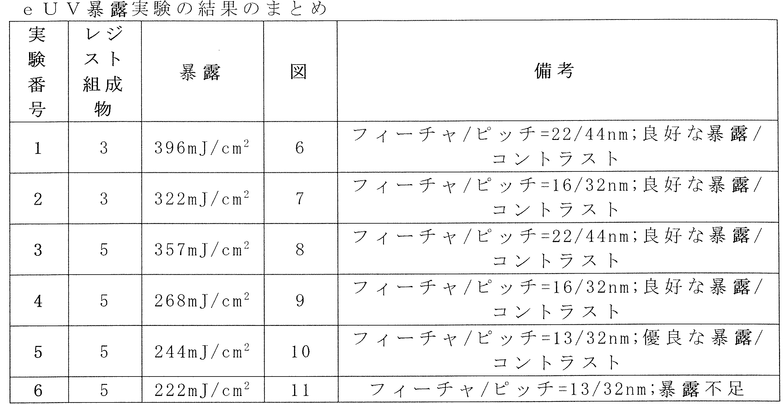
実験5は、優勢な試験条件、すなわち244mJ/cm2で暴露されたヨウ化水銀誘導体で最善の結果をもたらした。一部の暴露におけるラインエッジラフネス(LER)は、フォトマスクによって課せられる品質の制限によるものである。
HgCl2および/またはHgI2などの二次電子発生剤を組み込むことで、解像度を損なうことなくレジストの感度が改善された。例えば、本発明者らは、HgI2を使用すると、HgI2を含まない同等の配合物と比較して、少なくとも1.32倍感度が改善されることを見出した。これは、暴露中に必要とされるより低い暴露量に反映される。 Incorporating secondary electron generators such as HgCl2 and/or HgI2 improved the sensitivity of the resist without compromising resolution. For example, we found that the use of HgI2 improved sensitivity by at least 1.32 times compared to a comparable formulation without HgI2 . This is reflected in the lower exposure required during exposure .
図12は、現在開発されている6世代のレジストコーティングを通って減少する(したがって感度が増加する)必要な暴露線量を示すグラフであり、コーティングのそれぞれの6世代は以下のとおりである:
第1世代-化合物1の60nm厚のレジストコーティング(二次電子発生剤なし)
第2世代-化合物3の60nm厚のレジストコーティング
第3世代-化合物5の60nm厚のレジストコーティング
第4世代-化合物3の50nm厚のレジストコーティング
第5世代-化合物3の20nm厚のレジストコーティング
第6世代-化合物5の20nm厚のレジストコーティング
FIG. 12 is a graph showing the required exposure dose decreasing (and thus increasing sensitivity) through six generations of resist coatings currently in development, each of the six generations of coatings being:
1st generation - 60 nm thick resist coating of compound 1 (no secondary electron generator)
Generation 2 - 60 nm thick resist coating of
本発明者らは、上述の6世代のレジストをEUV照射線(エネルギー=92eV)に暴露させた。
We exposed the above mentioned
第1世代のレジスト材料は、990mJ/cm2の暴露線量を有し、これは所望のものよりも高い。二次電子発生剤および本発明のレジスト組成物へのこれらの組み込みの根底となる化学がよりよく理解されるにつれて、本発明者らはレジスト感度の顕著な改善を生み出すことができた。第6世代のレジストは、ライン暴露線量244mJ/cm2まで低減された暴露線量を呈した。この進捗は、図12のグラフに見ることができる。 First generation resist materials have an exposure dose of 990 mJ/cm 2 , which is higher than desired. As the chemistry underlying secondary electron generators and their incorporation into resist compositions of the invention became better understood, we were able to produce significant improvements in resist sensitivity. The sixth generation resist exhibited a reduced exposure dose to a line exposure dose of 244 mJ/cm 2 . This progress can be seen in the graph of FIG.
このように、二次電子発生剤(例えば、高Zeffおよび高密度金属化合物)を含めることは感度を高めるために望ましく、都合のよいことに、二次電子発生剤をレジスト化合物に配位させることが実施可能である。これにより、低密度レジスト組成物(例えば、主に散乱防止材料を有する)を本質的に提供して、高解像度を促進して、散乱を低減し、かつ、散発的な(かつ規則的な)高密度の領域を提供して、局所的な散乱を促進してレジスト感度を増加させる。 Thus, the inclusion of secondary electron generators (e.g., high Z eff and high density metal compounds) is desirable to enhance sensitivity, and is conveniently coordinated to the resist compound. is feasible. This inherently provides a low density resist composition (e.g., having predominantly anti-scattering materials) to facilitate high resolution, reduce scattering, and provide sporadic (and regular) A high density region is provided to promote localized scattering and increase resist sensitivity.
上記は、他のレジスト化合物、レジスト組成物、および他の二次電子発生剤に適用され得る広範な概念の単なる例であることは、当業者には理解されるであろう。二次電子発生剤構成成分に関しては、特許公開WO2015/145144(同じ発明者/出願人による)は、自由に分散した形態であるか、かつ/または散乱防止物質および/もしくはレジスト物質(複数可)に配位させるかのいずれかで、本発明のレジスト組成物に混合し得る好適な代替的二次電子発生剤の範囲を記述している。これに関して、WO2015/145144は、参照により本明細書に組み込まれる。 It will be appreciated by those skilled in the art that the above are merely examples of broad concepts that may be applied to other resist compounds, resist compositions, and other secondary electron generators. With respect to the secondary electron generator component, Patent Publication WO2015/145144 (by the same inventor/applicant) is in freely dispersed form and/or anti-scattering and/or resist material(s) describes a range of suitable alternative secondary electron generators that may be incorporated into the resist compositions of the invention, either by coordinating to In this regard, WO2015/145144 is incorporated herein by reference.
結論
上記の実験結果は、紫外波長の全範囲にわたる本発明のレジスト組成物の適応度を示す。このように、これらのレジストは、本明細書の他の箇所で概説した重要な利点(例えば、高解像度、感度、スピンコーティング性など)を提供するだけでなく、これらの利点を多方面にわたり、ある条件の範囲にわたって利用し、実現することができ、これによりその産業上の適用性が広がる。本発明のレジストは、電子回路および集積回路の分野に特別に貢献することとなり、本発明の利点は、最高品質の次世代の高性能エレクトロニクスを製造するために普遍的に実現され得る。
Conclusions The above experimental results demonstrate the suitability of the resist compositions of the present invention over the entire range of ultraviolet wavelengths. As such, these resists not only offer the important advantages outlined elsewhere herein (e.g., high resolution, sensitivity, spin-coatability, etc.), but also extend these advantages in many ways, including: It can be used and implemented over a range of conditions, which broadens its industrial applicability. The resist of the present invention will make a particular contribution to the field of electronic and integrated circuits, and the advantages of the present invention can be universally realized for producing the highest quality next generation high performance electronics.
参考文献
1)G.E.Moore,「Cramming more components onto intergrated circuits」,Electronics,38(80(1965年)
2)R.Mahajan,R.Nair,V.Wakharkar,J.Swan,G.Vandentop,「Emerging directions for packaging technologies」、Intel Technology Journal,6(2),pp.62-75、(2002年)
3)H.Bakoglu、「Circuit,interconnection and packaging for VLSI」Addison-Wesley publication Company,Reading MA,(1990年)
Reference 1)G. E. Moore, "Cramming more components onto integrated circuits," Electronics, 38 (80 (1965)).
2) R.I. Mahajan, R.; Nair, V.; Wakharkar, J.; Swan, G.; Vandentop, "Emerging directions for packaging technologies", Intel Technology Journal, 6(2), pp. 62-75, (2002)
3) H.I. Bakoglu, "Circuit, interconnection and packaging for VLSI," Addison-Wesley publication Company, Reading MA, (1990).
Claims (38)
a)前記散乱防止構成成分が前記フォトレジスト構成成分であり、
b)前記フォトレジスト構成成分が、前記散乱防止構成成分の一部であるか又は、それらと相互に会合されるか、若しくは化学的及び/又は物理的に、結合によって接続されるように、前記散乱防止構成成分が前記フォトレジスト構成成分を含み、又は
c)前記フォトレジスト構成成分が、前記散乱防止構成成分と別個の化合物である
のいずれかである、請求項1に記載のフォトレジスト組成物。 the metal ions are not boron and silicon ,
a) said anti-scatter component is said photoresist component;
b) said photoresist component is part of, or is mutually associated with, or chemically and/or physically connected to, said anti-scattering component by a bond; 2. The photoresist composition of claim 1, wherein the antiscatter component comprises the photoresist component, or c) the photoresist component is a separate compound from the antiscatter component. .
前記一次金属錯体は、2つ以上の異なる金属種(例えば、2つ以上の異なる金属イオン),M1及びM2,を含み、ここで、M1及びM2が、同じ金属元素から誘導されるが異なる原子価を有するか、または異なる金属元素から誘導され且つ同一もしくは異なる原子価を有する、
請求項1又は2に記載のフォトレジスト組成物。 the one or more ligands comprise a bridging ligand that bonds together multiple metal species within the primary metal complex; and
The primary metal complex comprises two or more different metal species (eg, two or more different metal ions), M 1 and M 2 , where M 1 and M 2 are derived from the same metal element. but have different valences, or are derived from different metallic elements and have the same or different valences ,
3. The photoresist composition of claim 1 or 2.
請求項1~3のいずれか1項に記載のフォトレジスト組成物。 all of the ligands of the primary metal complex are coordinated to the metal species via donor atoms or groups comprising heteroatoms having one or more lone pairs of electrons;
The photoresist composition of any one of claims 1-3.
請求項1~4のいずれか1項に記載のフォトレジスト組成物。 said primary metal complex comprises a mixture of two or more different types of ligands;
The photoresist composition of any one of claims 1-4.
請求項1~5のいずれか1項に記載のフォトレジスト組成物。 the anti-scattering compound comprises one or more counterions associated with the primary metal complex;
The photoresist composition of any one of claims 1-5.
請求項1~6のいずれか1項に記載のフォトレジスト組成物。 one or more photoresist components bonded to said primary metal complex via a coordination donor atom or group supported by said one or more photoresist ligands; said primary metal complex comprises or is otherwise associated with said one or more photoresist components in that
The photoresist composition of any one of claims 1-6.
請求項1~10のいずれか1項に記載のフォトレジスト組成物。 The one or more photoresist components are photosensitive components that undergo change upon exposure to relevant radiation and are capable of undergoing photolytic reactions without the aid of additional photoinitiators and photocatalysts. , otherwise comprising said photosensitive component,
The photoresist composition of any one of claims 1-10.
前記散乱防止-フォトレジストハイブリッド構成成分とは別の化合物であるか、又は
協調的に付着していることによる、散乱防止-フォトレジストハイブリッド構成成分の構成成分であるか、ここで、前記二次電子発生剤のZeffが、それが配位的に付着している分子を除外することによって計算される、
のいずれかである、
請求項1~11のいずれか1項に記載のフォトレジスト組成物。 The photoresist composition comprises a secondary electron generator (SEG), wherein the secondary electron generator has a Z eff of 25 or greater or an atomic number (Z) of 49 or greater and +1 or greater. A compound or component characterized by comprising a metal species having an oxidation state, wherein the secondary electron generator comprises:
is a separate compound from said anti-scatter-photoresist hybrid component, or is a component of said anti-scatter-photoresist hybrid component by virtue of being cooperatively attached, wherein said secondary Z eff of an electron generator is calculated by excluding the molecule to which it is coordinatively attached,
is either
The photoresist composition of any one of claims 1-11.
[Cr7Ni(O2CRB1)r];
式中、RB1は、π系を含む、置換されていてもよい(1~20C)ヒドロカルビル基であり、rは1以上の値を有する整数であり、式IIgの前記単位は、1つ以上の他の会合した配位子を含んでいてもよい、
によって定義される単位によって定義されるか、またはその単位を含む、請求項19に記載のフォトレジスト組成物。 The primary metal complex has the formula IIg below
[ Cr7Ni ( O2CRB1 ) r ];
wherein R B1 is an optionally substituted (1-20C) hydrocarbyl group containing a π-system, r is an integer having a value of 1 or greater , and said units of formula IIg are one or more may contain other associated ligands of
20. The photoresist composition of claim 19 defined by or comprising units defined by:
前記π系は、炭素-炭素二重結合または三重結合、炭素-ヘテロ原子二重結合または三重結合、芳香族またはヘテロ芳香族環系、炭素、又は炭素及び1つ以上のヘテロ原子を伴う共役π系、またはこれらの混合物を含む群から選択され、
前記1つ以上の配位供与原子または基は、1つ以上の孤立電子対担持ヘテロ原子を含む、請求項21に記載のフォトレジスト組成物。 each resist ligand comprises a crosslinkable pi-system and one or more coordination donor atoms or groups;
The π-system may be a carbon-carbon double or triple bond, a carbon-heteroatom double or triple bond, an aromatic or heteroaromatic ring system, carbon , or a conjugated π with carbon and one or more heteroatoms. system, or mixtures thereof,
22. The photoresist composition of claim 21, wherein said one or more coordination donor atoms or groups comprise one or more lone pair-bearing heteroatoms.
[Cr7NiF8(O2CRB1)r];式中、RB1は、末端アルケン部分を含む、置換されていてもよい(1~6C)ヒドロカルビル基であり、rは1以上の値を有する整数であり、式IIiの前記単位は、1つ以上の他の会合配位子(すなわち、前記錯体内に供与結合している)を含んでいてもよい、
によって定義される単位によって定義されるか、またはその単位を含む、請求項24に記載のフォトレジスト組成物。 Said primary metal complex has the formula IIi below:
[Cr 7 NiF 8 (O 2 CR B1 ) r ]; wherein R B1 is an optionally substituted (1-6C) hydrocarbyl group containing a terminal alkene moiety, and r has a value of 1 or greater; and said unit of formula IIi may contain one or more other associating ligands (i.e. datively bonded within said complex);
25. The photoresist composition of claim 24 defined by or comprising units defined by:
i)基板にフォトレジストコーティングを塗布するステップと、
ii)前記フォトレジストコーティングの1以上の部分を照射線に暴露させて、暴露されたフォトレジストコーティングをもたらすステップと、
iii)前記暴露されたフォトレジストコーティングを現像してレジストパターン層を生成するステップであって、前記レジストパターン層は、前記フォトレジストコーティングの現像液不溶性コーティング部分(すなわち隆起)と前記レジストパターン層を通って延在する溝の列と、を含む、ステップと
を含み、
前記フォトレジストコーティングは、乾燥および/または硬化されていてもよい請求項1~28のいずれか一項に記載のフォトレジスト組成物を含む、
前記方法。 A method of performing lithography, comprising:
i) applying a photoresist coating to the substrate;
ii) exposing one or more portions of the photoresist coating to radiation resulting in an exposed photoresist coating;
iii) developing said exposed photoresist coating to produce a patterned resist layer, said patterned resist layer comprising developer insoluble coating portions (i.e. ridges) of said photoresist coating and said patterned resist layer; a row of grooves extending through a step;
including _
wherein said photoresist coating comprises a photoresist composition according to any one of claims 1 to 28, optionally dried and/or cured;
the aforementioned method.
i)基板にフォトレジストコーティングを塗布するステップと、
ii)前記フォトレジストコーティングの1以上の部分を照射線に暴露させて、暴露されたフォトレジストコーティングをもたらすステップと、
iii)前記暴露されたフォトレジストコーティングを現像してレジストパターン層を生成するステップであって、前記レジストパターン層は、前記フォトレジストコーティングの現像液不溶性コーティング部分と前記レジストパターン層を通って延在する溝の列と、を含む、ステップと
を含み、
前記フォトレジストコーティングは、乾燥および/または硬化されていてもよい請求項1~28のいずれか一項に記載のフォトレジスト組成物を含む、
前記方法。 A method of manufacturing a lithographic mask, comprising:
i) applying a photoresist coating to the substrate;
ii) exposing one or more portions of the photoresist coating to radiation resulting in an exposed photoresist coating;
iii) developing said exposed photoresist coating to produce a patterned resist layer, said patterned resist layer extending through a developer-insoluble coating portion of said photoresist coating and said patterned resist layer; including a row of grooves and a step and
including
wherein said photoresist coating comprises a photoresist composition according to any one of claims 1 to 28, optionally dried and/or cured;
the aforementioned method.
i)基板にレジストコーティングを塗布するステップと、
ii)前記レジストコーティングの1以上の部分を照射線(例えば、UV)に暴露させて、暴露されたレジストコーティングをもたらすステップと、
或いは、
i)基板にレジストコーティングを塗布し、請求項31に記載のリソグラフィマスクを製造する方法によってリソグラフィマスクを提供すること、
ii)前記レジストコーティングの1以上の部分を照射線(例えば、UVまたは可視光線)に暴露させて、暴露されたレジストコーティングをもたらすステップと、
並びに、
iii)前記暴露されたフォトレジストコーティング又は前記暴露されたレジストコーティングを現像してレジストパターン層を生成するステップであって、前記レジストパターン層は、前記フォトレジストコーティング又は前記レジストコーティングの現像液不溶性コーティング部分(すなわち隆起)と前記レジストパターン層を通って延在する溝の列と、を含む、ステップと、
iv)前記レジストパターン層の下にある前記基板、基板表面またはその1以上の部分を改変するステップ(これには、前記ダイまたは前記各ダイの前記電子部品を1以上の導体に導電的に相互接続することを伴い得る)と、
v)前記レジストパターン層を除去して改変された基板を提供するステップと、
を含み、前記フォトレジストレジストコーティングは、乾燥および/または硬化されていてもよい請求項1~28のいずれか一項に記載のフォトレジスト組成物を含み、
前記レジストコーティングが、前記フォトレジストコーティング又は代替的レジストコーティングのいずれかである、
前記方法。 1. A method of making an integrated circuit die or an integrated circuit wafer including a plurality of integrated circuit dies, the or each die including a plurality of electronic components, the method comprising:
i) applying a resist coating to the substrate;
ii) exposing one or more portions of the resist coating to radiation (e.g., UV) to provide an exposed resist coating;
or
i) applying a resist coating to a substrate to provide a lithographic mask by the method of manufacturing a lithographic mask according to claim 31;
ii) exposing one or more portions of the resist coating to radiation (e.g., UV or visible light) to provide an exposed resist coating;
and,
iii) developing the exposed photoresist coating or the exposed resist coating to produce a patterned resist layer, wherein the patterned resist layer is a developer-insoluble coating of the photoresist coating or the resist coating; portions (i.e. ridges) and rows of grooves extending through the resist pattern layer;
iv) modifying the substrate, substrate surface, or one or more portions thereof underlying the resist pattern layer, including conductively interconnecting the electronic components of the or each die to one or more conductors; connecting) and
v) removing said patterned resist layer to provide a modified substrate;
wherein the photoresist resist coating comprises a photoresist composition according to any one of claims 1 to 28, which may be dried and/or cured;
wherein said resist coating is either said photoresist coating or an alternative resist coating;
the aforementioned method.
i)請求項32に記載の集積回路ダイを作る方法によって集積回路ダイを作るステップと、
ii)前記集積回路ダイをパッケージ基板に取り付けるステップと、ここで、前記パッケージ基板は電気接点を含み、前記電気接点の各々は、対応するピンに接続されるかまたは接続可能である、
iii)前記集積回路ダイの前記外部接触端子の各々を前記パッケージ基板の対応する電気接点に導電的に接続するステップと、
iv)前記パッケージ基板の前記電気接点を対応するピンに接続するステップと、
v)前記集積回路ダイをカプセル封入するステップと
を含む、前記方法。 A method of manufacturing an integrated circuit package, the integrated circuit package comprising an integrated circuit die having a plurality of pins and external contact terminals conductively connected to a corresponding plurality of pins, the method comprising:
i) making an integrated circuit die by the method of making an integrated circuit die of claim 32;
ii) attaching the integrated circuit die to a package substrate, wherein the package substrate includes electrical contacts, each of the electrical contacts being connected or connectable to a corresponding pin;
iii) conductively connecting each of said external contact terminals of said integrated circuit die to a corresponding electrical contact of said package substrate;
iv) connecting the electrical contacts of the package substrate to corresponding pins;
v) encapsulating said integrated circuit die.
i)請求項33に記載の集積回路パッケージを製造する方法によって集積回路パッケージを製造するステップと、
ii)前記集積回路パッケージを回路基板に導電的に接続するステップと
を含む、前記方法。 A method of manufacturing a circuit board including an integrated circuit package including a plurality of pins, comprising:
i) manufacturing an integrated circuit package by the method of manufacturing an integrated circuit package of claim 33;
ii) conductively connecting the integrated circuit package to a circuit board.
i)請求項34に記載の回路基板の製造方法によって回路基板を製造するステップと、
ii)前記電子デバイスまたはシステム内に前記回路基板を組み込むステップと
を含む、前記方法。 A method of manufacturing an electronic device or system, said electronic device or system comprising a circuit board comprising or connectable to a power source and conductively connected or connectable to a power source. with
i) manufacturing a circuit board by the method of manufacturing a circuit board according to claim 34;
ii) incorporating said circuit board within said electronic device or system.
Priority Applications (1)
| Application Number | Priority Date | Filing Date | Title |
|---|---|---|---|
| JP2022141770A JP2022184876A (en) | 2015-09-30 | 2022-09-06 | photoresist composition |
Applications Claiming Priority (3)
| Application Number | Priority Date | Filing Date | Title |
|---|---|---|---|
| GB1517273.7 | 2015-09-30 | ||
| GBGB1517273.7A GB201517273D0 (en) | 2015-09-30 | 2015-09-30 | Resist composition |
| PCT/GB2016/053032 WO2017055850A1 (en) | 2015-09-30 | 2016-09-29 | Resist composition |
Related Child Applications (1)
| Application Number | Title | Priority Date | Filing Date |
|---|---|---|---|
| JP2022141770A Division JP2022184876A (en) | 2015-09-30 | 2022-09-06 | photoresist composition |
Publications (3)
| Publication Number | Publication Date |
|---|---|
| JP2018533060A JP2018533060A (en) | 2018-11-08 |
| JP2018533060A5 JP2018533060A5 (en) | 2020-04-02 |
| JP7138564B2 true JP7138564B2 (en) | 2022-09-16 |
Family
ID=54544334
Family Applications (2)
| Application Number | Title | Priority Date | Filing Date |
|---|---|---|---|
| JP2018516193A Active JP7138564B2 (en) | 2015-09-30 | 2016-09-29 | photoresist composition |
| JP2022141770A Pending JP2022184876A (en) | 2015-09-30 | 2022-09-06 | photoresist composition |
Family Applications After (1)
| Application Number | Title | Priority Date | Filing Date |
|---|---|---|---|
| JP2022141770A Pending JP2022184876A (en) | 2015-09-30 | 2022-09-06 | photoresist composition |
Country Status (8)
| Country | Link |
|---|---|
| US (2) | US11143961B1 (en) |
| EP (1) | EP3356889A1 (en) |
| JP (2) | JP7138564B2 (en) |
| KR (1) | KR20180063182A (en) |
| CN (2) | CN115373220B (en) |
| GB (1) | GB201517273D0 (en) |
| TW (2) | TWI737629B (en) |
| WO (1) | WO2017055850A1 (en) |
Families Citing this family (15)
| Publication number | Priority date | Publication date | Assignee | Title |
|---|---|---|---|---|
| GB201405335D0 (en) * | 2014-03-25 | 2014-05-07 | Univ Manchester | Resist composition |
| GB201413924D0 (en) | 2014-08-06 | 2014-09-17 | Univ Manchester | Electron beam resist composition |
| GB201517273D0 (en) | 2015-09-30 | 2015-11-11 | Univ Manchester | Resist composition |
| KR102498632B1 (en) * | 2018-08-16 | 2023-02-10 | 주식회사 엘지화학 | Preparation method of substrate |
| WO2020045302A1 (en) * | 2018-08-30 | 2020-03-05 | 東京エレクトロン株式会社 | Substrate processing method and substrate processing device |
| JP2020201480A (en) * | 2019-06-05 | 2020-12-17 | Jsr株式会社 | Radiation-sensitive composition, pattern forming method, and compound |
| TWI780715B (en) * | 2020-05-21 | 2022-10-11 | 台灣積體電路製造股份有限公司 | Method of manufacturing a semiconductor device and developer composition |
| US12153346B2 (en) * | 2020-09-30 | 2024-11-26 | Taiwan Semiconductor Manufacturing Company, Ltd. | Photoresist for semiconductor fabrication |
| US11726405B2 (en) * | 2020-09-30 | 2023-08-15 | Taiwan Semiconductor Manufacturing Company, Ltd. | Photoresist for semiconductor fabrication |
| KR102903553B1 (en) | 2021-03-19 | 2025-12-22 | 삼성전자 주식회사 | Method of fabricating semiconductor device |
| CN114613672A (en) * | 2022-05-16 | 2022-06-10 | 广州粤芯半导体技术有限公司 | Method for manufacturing semiconductor device |
| WO2024106832A1 (en) * | 2022-11-16 | 2024-05-23 | 광주과학기술원 | Photoresist composition for euv, method for manufacturing same, and method for forming photoresist pattern using same |
| CN115926189B (en) * | 2023-01-12 | 2023-11-10 | 台州学院 | A composite material HKUST-1@PQ and its preparation method |
| CN116589691B (en) * | 2023-04-27 | 2026-01-30 | 中国科学院赣江创新研究院 | A method for preparing rare earth-based spherical MOFs and its application |
| TWI867910B (en) * | 2023-12-22 | 2024-12-21 | 財團法人工業技術研究院 | Photosensitive dry film, composition solution for forming thereof, and method for electroless plating metal layer |
Citations (1)
| Publication number | Priority date | Publication date | Assignee | Title |
|---|---|---|---|---|
| JP2016530565A (en) | 2013-08-22 | 2016-09-29 | インプリア・コーポレイションInpria Corporation | High resolution patterning compositions based on organometallic solutions |
Family Cites Families (44)
| Publication number | Priority date | Publication date | Assignee | Title |
|---|---|---|---|---|
| SE361366B (en) * | 1968-10-03 | 1973-10-29 | Western Electric Co | |
| GB1535258A (en) * | 1975-05-22 | 1978-12-13 | Outboard Marine Corp | Internal combustion engines and method of operation thereof |
| US4463265A (en) * | 1982-06-17 | 1984-07-31 | Hewlett-Packard Company | Electron beam proximity effect correction by reverse field pattern exposure |
| US4517276A (en) * | 1982-11-29 | 1985-05-14 | Varian Associates, Inc. | Metal-containing organic photoresists |
| US4464458A (en) * | 1982-12-30 | 1984-08-07 | International Business Machines Corporation | Process for forming resist masks utilizing O-quinone diazide and pyrene |
| US4737425A (en) * | 1986-06-10 | 1988-04-12 | International Business Machines Corporation | Patterned resist and process |
| EP0307919B1 (en) * | 1987-09-16 | 1993-05-19 | Canon Kabushiki Kaisha | Resin composition curable with an active energy ray containing epoxy resin and monomer with ethylenically unsaturated bond |
| US5079131A (en) * | 1988-08-29 | 1992-01-07 | Shipley Company Inc. | Method of forming positive images through organometallic treatment of negative acid hardening cross-linked photoresist formulations |
| EP0413087A1 (en) * | 1989-07-20 | 1991-02-20 | International Business Machines Corporation | Photosensitive composition and use thereof |
| US5164278A (en) * | 1990-03-01 | 1992-11-17 | International Business Machines Corporation | Speed enhancers for acid sensitized resists |
| US5296330A (en) * | 1991-08-30 | 1994-03-22 | Ciba-Geigy Corp. | Positive photoresists containing quinone diazide photosensitizer, alkali-soluble resin and tetra(hydroxyphenyl) alkane additive |
| US5382637A (en) * | 1991-10-31 | 1995-01-17 | International Business Machines Corporation | Solid state chain extension polymerization between Lewis acid oligomers and deblocked Lewis bases |
| US6147184A (en) * | 1992-03-23 | 2000-11-14 | Rhone-Poulenc Chimie | Onium borates/borates of organometallic complexes and cationic initiation of polymerization therewith |
| US5548034A (en) * | 1992-07-31 | 1996-08-20 | International Business Machines Corporation | Modified dicyanate ester resins having enhanced fracture toughness |
| KR100294715B1 (en) * | 1995-09-14 | 2001-09-17 | 포만 제프리 엘 | Cured Photosensitive Polycyanurate Resist, Structures Produced therefrom and Method of Making the Same |
| JP3628098B2 (en) * | 1996-03-29 | 2005-03-09 | ダウ コーニング アジア株式会社 | Radiation curable composition and method for producing cured product pattern using the same |
| US5986508A (en) | 1996-08-26 | 1999-11-16 | Nevin; Larry J. | Bias concept for intrinsic gain stabilization over temperature |
| US5976770A (en) * | 1998-01-15 | 1999-11-02 | Shipley Company, L.L.C. | Dyed photoresists and methods and articles of manufacture comprising same |
| US6171757B1 (en) * | 1999-07-12 | 2001-01-09 | International Business Machines Corporation | Organometallic polymers and use thereof |
| US6436605B1 (en) * | 1999-07-12 | 2002-08-20 | International Business Machines Corporation | Plasma resistant composition and use thereof |
| US7074640B2 (en) * | 2000-06-06 | 2006-07-11 | Simon Fraser University | Method of making barrier layers |
| US6617186B2 (en) * | 2000-09-25 | 2003-09-09 | Dai Nippon Printing Co., Ltd. | Method for producing electroluminescent element |
| US7008749B2 (en) | 2001-03-12 | 2006-03-07 | The University Of North Carolina At Charlotte | High resolution resists for next generation lithographies |
| JP4178360B2 (en) * | 2001-06-14 | 2008-11-12 | 信越化学工業株式会社 | Novel epoxy compound having alicyclic structure, polymer compound, resist material, and pattern forming method |
| US6841883B1 (en) * | 2003-03-31 | 2005-01-11 | Micron Technology, Inc. | Multi-dice chip scale semiconductor components and wafer level methods of fabrication |
| JP4507775B2 (en) | 2004-09-10 | 2010-07-21 | 凸版印刷株式会社 | Manufacturing method of stencil mask |
| TW200634055A (en) | 2004-12-07 | 2006-10-01 | Hybrid Plastics Inc | Process for highly purified polyhedral oligomeric silsesquioxane monomers |
| US7393770B2 (en) * | 2005-05-19 | 2008-07-01 | Micron Technology, Inc. | Backside method for fabricating semiconductor components with conductive interconnects |
| JP2007086368A (en) | 2005-09-21 | 2007-04-05 | Fujitsu Ltd | Photomask, photomask manufacturing method, and semiconductor device manufacturing method |
| TW200717176A (en) * | 2005-09-21 | 2007-05-01 | Dainippon Printing Co Ltd | Photo mask having gradation sequence and method for manufacturing the same |
| JP5343340B2 (en) * | 2007-10-05 | 2013-11-13 | Jsr株式会社 | Radiation sensitive resin composition |
| JP2009258357A (en) * | 2008-04-16 | 2009-11-05 | Geomatec Co Ltd | Substrate for photomask, photomask, and method of manufacturing the same |
| JP5293168B2 (en) | 2008-12-25 | 2013-09-18 | 富士通株式会社 | Resist composition and method for manufacturing semiconductor device using the same |
| WO2012118847A2 (en) | 2011-02-28 | 2012-09-07 | Inpria Corportion | Solution processible hardmarks for high resolusion lithography |
| FR2979165B1 (en) * | 2011-08-16 | 2014-05-16 | Commissariat Energie Atomique | METHOD FOR CORRECTING ELECTRONIC PROXIMITY EFFECTS USING DECENTRED DIFFUSION FUNCTIONS |
| US9362126B2 (en) * | 2011-09-22 | 2016-06-07 | Agency For Science, Technology And Research | Process for making a patterned metal oxide structure |
| US8703386B2 (en) * | 2012-02-27 | 2014-04-22 | International Business Machines Corporation | Metal peroxo compounds with organic co-ligands for electron beam, deep UV and extreme UV photoresist applications |
| GB201413924D0 (en) * | 2014-08-06 | 2014-09-17 | Univ Manchester | Electron beam resist composition |
| KR102952227B1 (en) | 2014-10-23 | 2026-04-13 | 인프리아 코포레이션 | Organometallic solution based high resolution patterning compositions and corresponding methods |
| US10468249B2 (en) * | 2015-09-28 | 2019-11-05 | Taiwan Semiconductor Manufacturing Company, Ltd. | Patterning process of a semiconductor structure with a middle layer |
| GB201517273D0 (en) | 2015-09-30 | 2015-11-11 | Univ Manchester | Resist composition |
| KR102508142B1 (en) | 2015-10-13 | 2023-03-08 | 인프리아 코포레이션 | Organotin oxide hydroxide patterning compositions, precursors, and patterning |
| KR102394042B1 (en) | 2016-03-11 | 2022-05-03 | 인프리아 코포레이션 | Pre-patterned lithographic templates, methods based on radiation patterning using said templates and methods for forming said templates |
| KR102610448B1 (en) | 2016-08-12 | 2023-12-07 | 인프리아 코포레이션 | Methods of reducing metal residue in edge bead region from metal-containing resists |
-
2015
- 2015-09-30 GB GBGB1517273.7A patent/GB201517273D0/en not_active Ceased
-
2016
- 2016-09-29 EP EP16777763.0A patent/EP3356889A1/en active Pending
- 2016-09-29 US US15/764,584 patent/US11143961B1/en active Active
- 2016-09-29 CN CN202210945261.5A patent/CN115373220B/en active Active
- 2016-09-29 JP JP2018516193A patent/JP7138564B2/en active Active
- 2016-09-29 TW TW105131426A patent/TWI737629B/en active
- 2016-09-29 KR KR1020187011901A patent/KR20180063182A/en not_active Ceased
- 2016-09-29 WO PCT/GB2016/053032 patent/WO2017055850A1/en not_active Ceased
- 2016-09-29 TW TW110131029A patent/TWI796763B/en active
- 2016-09-29 CN CN201680062388.5A patent/CN108351587B/en active Active
-
2021
- 2021-07-23 US US17/384,066 patent/US20220179319A1/en not_active Abandoned
-
2022
- 2022-09-06 JP JP2022141770A patent/JP2022184876A/en active Pending
Patent Citations (1)
| Publication number | Priority date | Publication date | Assignee | Title |
|---|---|---|---|---|
| JP2016530565A (en) | 2013-08-22 | 2016-09-29 | インプリア・コーポレイションInpria Corporation | High resolution patterning compositions based on organometallic solutions |
Also Published As
| Publication number | Publication date |
|---|---|
| CN115373220A (en) | 2022-11-22 |
| TWI737629B (en) | 2021-09-01 |
| JP2018533060A (en) | 2018-11-08 |
| GB201517273D0 (en) | 2015-11-11 |
| TWI796763B (en) | 2023-03-21 |
| KR20180063182A (en) | 2018-06-11 |
| TW202223540A (en) | 2022-06-16 |
| TW201730670A (en) | 2017-09-01 |
| EP3356889A1 (en) | 2018-08-08 |
| US20220179319A1 (en) | 2022-06-09 |
| CN108351587A (en) | 2018-07-31 |
| CN108351587B (en) | 2022-08-19 |
| US11143961B1 (en) | 2021-10-12 |
| JP2022184876A (en) | 2022-12-13 |
| CN115373220B (en) | 2025-10-31 |
| WO2017055850A1 (en) | 2017-04-06 |
Similar Documents
| Publication | Publication Date | Title |
|---|---|---|
| JP7138564B2 (en) | photoresist composition | |
| USRE50296E1 (en) | Electron beam resist composition | |
| JP5474290B2 (en) | Metal patterning method using precursor-containing nanoparticles | |
| US9372402B2 (en) | Molecular organometallic resists for EUV | |
| TWI244506B (en) | Method for depositing metal and metal oxide films and patterned films | |
| Sharps et al. | Organotin carboxylate reagents for nanopatterning: chemical transformations during direct-write electron beam processes | |
| Wu et al. | Fluorescent labeling to investigate nanopatterning processes in extreme ultraviolet lithography | |
| TW201602711A (en) | combination | |
| CN106170736A (en) | fullerene | |
| US20180373143A1 (en) | Sensitivity enhanced photoresists | |
| KR100765684B1 (en) | Organometallic Precursor Mixture for Alloy Pattern Formation and Alloy Pattern Formation Method Using the Same | |
| Wang et al. | Advances in metal-based photoresist materials for EUV lithography and lithographic mechanisms | |
| CN116009373B (en) | A holographic plate, its preparation method and application |
Legal Events
| Date | Code | Title | Description |
|---|---|---|---|
| A621 | Written request for application examination |
Free format text: JAPANESE INTERMEDIATE CODE: A621 Effective date: 20190927 |
|
| A524 | Written submission of copy of amendment under article 19 pct |
Free format text: JAPANESE INTERMEDIATE CODE: A524 Effective date: 20200220 |
|
| A977 | Report on retrieval |
Free format text: JAPANESE INTERMEDIATE CODE: A971007 Effective date: 20200826 |
|
| A131 | Notification of reasons for refusal |
Free format text: JAPANESE INTERMEDIATE CODE: A131 Effective date: 20201014 |
|
| A601 | Written request for extension of time |
Free format text: JAPANESE INTERMEDIATE CODE: A601 Effective date: 20210112 |
|
| A601 | Written request for extension of time |
Free format text: JAPANESE INTERMEDIATE CODE: A601 Effective date: 20210225 |
|
| A521 | Request for written amendment filed |
Free format text: JAPANESE INTERMEDIATE CODE: A523 Effective date: 20210412 |
|
| A131 | Notification of reasons for refusal |
Free format text: JAPANESE INTERMEDIATE CODE: A131 Effective date: 20211007 |
|
| A601 | Written request for extension of time |
Free format text: JAPANESE INTERMEDIATE CODE: A601 Effective date: 20211221 |
|
| A601 | Written request for extension of time |
Free format text: JAPANESE INTERMEDIATE CODE: A601 Effective date: 20220217 |
|
| A521 | Request for written amendment filed |
Free format text: JAPANESE INTERMEDIATE CODE: A523 Effective date: 20220404 |
|
| TRDD | Decision of grant or rejection written | ||
| A01 | Written decision to grant a patent or to grant a registration (utility model) |
Free format text: JAPANESE INTERMEDIATE CODE: A01 Effective date: 20220808 |
|
| A61 | First payment of annual fees (during grant procedure) |
Free format text: JAPANESE INTERMEDIATE CODE: A61 Effective date: 20220906 |
|
| R150 | Certificate of patent or registration of utility model |
Ref document number: 7138564 Country of ref document: JP Free format text: JAPANESE INTERMEDIATE CODE: R150 |
|
| R250 | Receipt of annual fees |
Free format text: JAPANESE INTERMEDIATE CODE: R250 |