JP7129630B2 - Light-emitting element and method for manufacturing light-emitting element - Google Patents
Light-emitting element and method for manufacturing light-emitting element Download PDFInfo
- Publication number
- JP7129630B2 JP7129630B2 JP2020050778A JP2020050778A JP7129630B2 JP 7129630 B2 JP7129630 B2 JP 7129630B2 JP 2020050778 A JP2020050778 A JP 2020050778A JP 2020050778 A JP2020050778 A JP 2020050778A JP 7129630 B2 JP7129630 B2 JP 7129630B2
- Authority
- JP
- Japan
- Prior art keywords
- layer
- type
- gan layer
- light
- doped
- Prior art date
- Legal status (The legal status is an assumption and is not a legal conclusion. Google has not performed a legal analysis and makes no representation as to the accuracy of the status listed.)
- Active
Links
Images


Description
本発明は、発光素子および発光素子の製造方法に関する。 The present invention relates to a light-emitting device and a method for manufacturing a light-emitting device.
特許文献1には、窒化物半導体の半導体積層構造中に、高濃度にp型不純物がドープされたp型GaNと、高濃度にn型不純物がドープされたn型GaN層とのトンネル接合を含む発光素子が開示されている。このような発光素子において、駆動電圧をさらに低減させることが望まれている。
本発明は、窒化物半導体の半導体積層構造中にトンネル接合を形成しつつ、駆動電圧を低減させることができる発光素子および発光素子の製造方法を提供することを目的とする。 SUMMARY OF THE INVENTION An object of the present invention is to provide a light-emitting device and a method for manufacturing a light-emitting device capable of reducing a driving voltage while forming a tunnel junction in a semiconductor laminated structure of a nitride semiconductor.
本発明の一態様によれば、発光素子は、n型不純物がドープされた第1のn型窒化物半導体層と、前記第1のn型窒化物半導体層上に設けられた第1の発光層と、前記第1の発光層上に設けられ、p型不純物がドープされたp型GaN層と、前記p型GaN層上に設けられ、前記第1のn型窒化物半導体層よりも高い不純物濃度のn型不純物がドープされたn型GaN層と、前記p型GaN層と前記n型GaN層との間に設けられ、前記n型GaN層と前記p型GaN層とが形成する空乏層の幅以下の厚さを有するノンドープGaN層と、前記n型GaN層上に設けられ、n型不純物がドープされた第2のn型窒化物半導体層と、前記第2のn型窒化物半導体層上に設けられた第2の発光層と、前記第2の発光層上に設けられ、p型不純物がドープされたp型窒化物半導体層と、を備える。
本発明の一態様によれば、発光素子の製造方法は、n型不純物がドープされた第1のn型窒化物半導体層を形成する工程と、前記第1のn型窒化物半導体層上に、第1の発光層を形成する工程と、前記第1の発光層上に、p型不純物がドープされたp型GaN層を形成する工程と、前記p型GaN層上に、ノンドープGaN層を含む中間層を形成する工程と、前記中間層上に、前記第1のn型窒化物半導体層よりも高い不純物濃度のn型不純物がドープされたn型GaN層を形成する工程と、前記n型GaN層上に、n型不純物がドープされた第2のn型窒化物半導体層を形成する工程と、前記第2のn型窒化物半導体層上に、第2の発光層を形成する工程と、前記第2の発光層上に、p型不純物がドープされたp型窒化物半導体層を形成する工程と、を備え、前記中間層を、前記n型GaN層と前記p型GaN層とが形成する空乏層の幅以下の厚さで形成する。
According to one aspect of the present invention, a light emitting device includes a first n-type nitride semiconductor layer doped with an n-type impurity, and a first light emitting device provided on the first n-type nitride semiconductor layer. a p-type GaN layer doped with p-type impurities provided on the first light-emitting layer; and a p-type GaN layer provided on the p-type GaN layer and higher than the first n-type nitride semiconductor layer. an n-type GaN layer doped with an n-type impurity having an impurity concentration, and a depletion layer provided between the p-type GaN layer and the n-type GaN layer and formed by the n-type GaN layer and the p-type GaN layer. a non-doped GaN layer having a thickness equal to or less than the width of the layer; a second n-type nitride semiconductor layer provided on the n-type GaN layer and doped with an n-type impurity; and the second n-type nitride. A second light emitting layer provided on a semiconductor layer, and a p-type nitride semiconductor layer provided on the second light emitting layer and doped with a p-type impurity.
According to one aspect of the present invention, a method for manufacturing a light-emitting device includes the steps of: forming a first n-type nitride semiconductor layer doped with an n-type impurity; forming a first light-emitting layer; forming a p-type GaN layer doped with a p-type impurity on the first light-emitting layer; forming a non-doped GaN layer on the p-type GaN layer; forming an intermediate layer containing n forming a second n-type nitride semiconductor layer doped with an n-type impurity on a GaN layer; and forming a second light emitting layer on the second n-type nitride semiconductor layer. and forming a p-type impurity-doped p-type nitride semiconductor layer on the second light-emitting layer, wherein the intermediate layer is composed of the n-type GaN layer and the p-type GaN layer. is formed with a thickness equal to or less than the width of the depletion layer formed by .
本発明によれば、窒化物半導体の半導体積層構造中にトンネル接合を形成しつつ、駆動電圧を低減させることができる発光素子および発光素子の製造方法を提供することができる。 ADVANTAGE OF THE INVENTION According to this invention, the manufacturing method of the light emitting element and the light emitting element which can reduce a drive voltage can be provided, forming a tunnel junction in the semiconductor laminated structure of a nitride semiconductor.
以下、図面を参照し、本発明の一実施形態について説明する。なお、各図面中、同じ要素には同じ符号を付している。 An embodiment of the present invention will be described below with reference to the drawings. In addition, the same code|symbol is attached|subjected to the same element in each drawing.
図1は、本発明の一実施形態の発光素子の模式断面図である。 FIG. 1 is a schematic cross-sectional view of a light-emitting device according to one embodiment of the present invention.
図1に示すように、実施形態の発光素子1は、基板11と、基板11上に設けられた半導体積層体10と、n側電極41と、p側電極42とを有する。
As shown in FIG. 1 , the
半導体積層体10は、窒化物半導体からなる複数の半導体層が積層された積層体である。本明細書において「窒化物半導体」とは、InxAlyGa1-x-yN(0≦x≦1,0≦y≦1,x+y≦1)なる化学式において組成比x及びyをそれぞれの範囲内で変化させた全ての組成の半導体を含むものとする。
The
半導体積層体10は、基板11上に、例えばMOCVD(metal organic chemical vapor deposition)法によりエピタキシャル成長される。基板11の材料は、例えば、サファイア、シリコン、SiC、GaNなどである。
The
半導体積層体10は、第1のn型窒化物半導体層12と、第1の発光層13と、第1のp型窒化物半導体層14と、p型GaN層15と、中間層20と、n型GaN層16と、第2のn型窒化物半導体層17と、第2の発光層18と、第2のp型窒化物半導体層19とを基板11側から順に有する。
The
基板11上に、第1のn型窒化物半導体層12、第1の発光層13、第1のp型窒化物半導体層14、p型GaN層15、中間層20、n型GaN層16、第2のn型窒化物半導体層17、第2の発光層18、および第2のp型窒化物半導体層19が順にエピタキシャル成長される。
On
第1のn型窒化物半導体層12、n型GaN層16、および第2のn型窒化物半導体層17には、n型不純物として、例えばシリコン(Si)がドープされている。n型GaN層16のn型不純物濃度は、第1のn型窒化物半導体層12のn型不純物濃度および第2のn型窒化物半導体層17のn型不純物濃度よりも高い。これは、p型GaN層15とn型GaN層16との間でトンネル効果を得るためであり、n型不純物濃度を高くすることでn型GaN層16とp型GaN層15とが形成する空乏層の電位の傾きを急峻にすることできる。例えば、n型GaN層16のn型不純物濃度を第1のn型窒化物半導体層12と同様のn型不純物濃度とした場合、n型GaN層16とp型GaN層15とが形成する空乏層の電位の傾きを急峻にすることが難しく十分なトンネル効果を得ることができない。
The first n-type
第1のp型窒化物半導体層14、p型GaN層15、および第2のp型窒化物半導体層19には、p型不純物として、例えばマグネシウム(Mg)がドープされている。
The first p-type
第2のp型窒化物半導体層19上にp側電極42が設けられ、p側電極42は第2のp型窒化物半導体層19に電気的に接続している。
A p-
第1のn型窒化物半導体層12は、第1の発光層13、第1のp型窒化物半導体層14、p型GaN層15、中間層20、n型GaN層16、第2のn型窒化物半導体層17、第2の発光層18、および第2のp型窒化物半導体層19が積層されていないnコンタクト面12aを有する。そのnコンタクト面12a上にn側電極41が設けられ、n側電極41は第1のn型窒化物半導体層12に電気的に接続している。
The first n-type
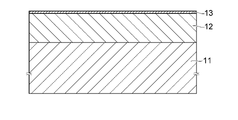
図2は、図1に示す発光素子1におけるp型GaN層15、中間層20、およびn型GaN層16が積層された部分の模式拡大断面図である。
FIG. 2 is a schematic enlarged cross-sectional view of a portion in which the p-
中間層20は、少なくともノンドープGaN層21を有する。図2に示す例では、中間層20はノンドープGaN層21から構成される。ノンドープGaN層21が、p型GaN層15とn型GaN層16との間に設けられている。
ここで、ノンドープ層とは、導電性を制御するための不純物を意図的にドープするための原料ガス(例えばSiやMgを含むガス)を用いることなく形成された層であり、プロセス上不可避的に混入される不純物を含む場合もある。例えば、ノンドープGaN層21の不純物濃度は、1×10¹⁸/cm3以下である。
Here, the non-doped layer is a layer formed without using a raw material gas (for example, a gas containing Si or Mg) for intentionally doping impurities for controlling conductivity, and is unavoidable in the process. It may contain impurities mixed in. For example, the impurity concentration of the
p側電極42には正電位が、n側電極41には負電位が印加される。このとき、第2のp型窒化物半導体層19とn型GaN層16との間には順方向電圧が印加され、第2の発光層18にホールおよび電子が供給されることで第2の発光層18が発光する。p型GaN層15と第1のn型窒化物半導体層12との間にも順方向電圧が印加され、第1の発光層13にホールおよび電子が供給されることで第1の発光層13が発光する。
A positive potential is applied to the p-
第1の発光層13の発光ピーク波長、および第2の発光層18の発光ピーク波長は、例えば、430nm以上540nm以下程度であり、青色光や緑色光を発する。第1の発光層13と第2の発光層18とを積層することで、1つの発光層が設けられている発光素子に比べて出力を高くすることができる。第1の発光層13及び第2発光層18の発光ピーク波長は、それぞれ異なっていてもよい。
The emission peak wavelength of the first light-emitting
p側電極42に正電位が、n側電極41に負電位が印加されたとき、n型GaN層16とp型GaN層15との間には逆方向電圧が印加されることになる。そのため、n型GaN層16とp型GaN層15との間の電流はトンネル効果を利用する。つまり、p型GaN層15の価電子帯に存在する電子をn型GaN層16とp型GaN層15との間の障壁をトンネリングさせることでn型GaN層16の伝導帯に移動させ電流を流す。
When a positive potential is applied to the p-
図4は、図2に示す積層部の模式的なエネルギーバンド図である。 FIG. 4 is a schematic energy band diagram of the laminated portion shown in FIG.
高濃度でn型不純物がドープされたn型GaN層16と、高濃度でp型不純物がドープされたp型GaN層15によりpn接合を形成し、n型GaN層16とp型GaN層15とが形成する空乏層の電位の傾きを急峻にして空乏層の幅を狭くする。このような構造とすることで、p型GaN層15の価電子帯の電子eが空乏層(電位障壁)をトンネリングしてn型GaN層16の伝導帯に移動させることができる。
A pn junction is formed by an n-
例えば、Siを不純物として含むn型GaN層16のSi濃度は、1×10²⁰/cm3以上1×1021/cm3以下である。Mgを不純物として含むp型GaN層15のMg濃度は1×1020/cm3以上1×1021/cm3以下である。このようなn型GaN層16とp型GaN層15とが形成する空乏層の幅は、例えば、7nm以上8nm以下である。
For example, the Si concentration of the n-
ノンドープGaN層21の厚さは、n型GaN層16とp型GaN層15とが形成する空乏層の幅以下の厚さであり、例えば、3nm以上5nm以下である。
The thickness of the
図6~図15は、図1に示す発光素子1の製造方法を示す模式断面図である。基板11上に前述した各層が、例えばMOCVD(metal organic chemical vapor deposition)法によりエピタキシャル成長される。
6 to 15 are schematic cross-sectional views showing a method of manufacturing the
まず、図6に示すように、基板11上に第1のn型窒化物半導体層12が形成される。図7に示すように、第1のn型窒化物半導体層12上には、第1の発光層13が形成される。図8に示すように、第1の発光層13上には、第1のp型窒化物半導体層14が形成される。図9に示すように、第1のp型窒化物半導体層14上には、p型GaN層15が形成される。図10に示すように、p型GaN層15上には、中間層20が形成される。図11に示すように、中間層20上には、n型GaN層16が形成される。図12に示すように、n型GaN層16上には、第2のn型窒化物半導体層17が形成される。図13に示すように、第2のn型窒化物半導体層17上には、第2の発光層18が形成される。図14に示すように、第2の発光層18上には、第2のp型窒化物半導体層19が形成される。このようにして、基板11上に半導体積層体10が形成される。
First, as shown in FIG. 6, the first n-type
この後、基板11上に形成された半導体積層体10の一部を除去して、図15に示すように、第1のn型窒化物半導体層12の一部としてnコンタクト面12aを露出させる。
Thereafter, a portion of the
その後、図1に示すように、第2のp型窒化物半導体層19上にp側電極42が形成され、nコンタクト面12a上にn側電極41が形成される。
Thereafter, as shown in FIG. 1, a p-
<実施例1>
以下に説明するように実施例に係る発光素子を作製した。
<Example 1>
A light-emitting device according to an example was fabricated as described below.
基板11上に、第1のn型窒化物半導体層12を形成した。基板11には、サファイアからなる基板を用いた。第1のn型窒化物半導体層12として、ノンドープのGaN層と、不純物としてSiを含むGaN層とを含む、膜厚が10μm程度の窒化物半導体層を形成した。
A first n-type
第1のn型窒化物半導体層12上に、第1の発光層13として、複数の井戸層と複数の障壁層を有する多重量子井戸層を形成した。膜厚が3.6nmであるノンドープのInGaN層からなる井戸層と、膜厚が4.3nmであるノンドープのGaN層からなる障壁層により形成し、井戸層と障壁層を1つのペアとして9ペア形成した。
A multiple quantum well layer having a plurality of well layers and a plurality of barrier layers was formed as the first
第1の発光層13上に、第1のp型窒化物半導体層14として、不純物としてMgを含むGaN層を含む膜厚が50nm程度の窒化物半導体層を形成した。
On the first
次に、第1のp型窒化物半導体層14上に、p型GaN層15としてMgの不純物濃度が1×10²⁰/cm3程度のGaN層を17nm程度形成した。その後、基板11及び基板11上の窒化物半導体層を含むウェーハに対する加熱温度を下げ、チャンバー内に残留したMgを含むガスを除去するパージ処理を行った後、ウェーハをチャンバー内から取り出す。この後、ウェーハをチャンバー内に戻し、昇温し、p型GaN層15上にノンドープGaN層21を3nm形成する。さらにウェーハに対する加熱温度を上げて、ノンドープGaN層21上にn型GaN層16として、Siの不純物濃度が1×1020/cm3程度であり膜厚が30nm程度であるGaN層を形成した。さらに、n型GaN層16上に、第2のn型窒化物半導体層17として、不純物としてSiを含む膜厚が100nm程度のGaN層を形成した。実施例1におけるp型GaN層15、n型GaN層16、及びノンドープGaN層21の積層構造は、図2で示した積層構造と同様である。
Next, a GaN layer having a Mg impurity concentration of about 1×10 20 /cm 3 was formed as a p-
<実施例2>
実施例2に係る発光素子は、ノンドープGaN層21の膜厚を5nmで形成した以外は実施例1と同様にして作製した。
<Example 2>
A light-emitting device according to Example 2 was fabricated in the same manner as in Example 1, except that the film thickness of the
<実施例3>
実施例3に係る発光素子は、ノンドープGaN層21の膜厚を1nmで形成した以外は実施例1と同様にして作製した。
<Example 3>
A light-emitting device according to Example 3 was fabricated in the same manner as in Example 1, except that the film thickness of the
以上のように作製した実施例1~3に係る発光素子の第1のn型窒化物半導体層12と第2のn型窒化物半導体層17との間に電圧を印加し、駆動電圧を測定した。
A voltage is applied between the first n-type
<比較例>
比較例に係る発光素子は、ノンドープGaN層21を形成せずにp型GaN層15上に直接n型GaN層16を形成した以外は、実施例1と同様にして作製した。実施例に係る発光素子と同様に、比較例に係る発光素子の第1のn型窒化物半導体層12と第2のn型窒化物半導体層17との間に電圧を印加し、駆動電圧を測定した。
<Comparative example>
A light-emitting device according to a comparative example was fabricated in the same manner as in Example 1, except that the n-
実施例1に係る発光素子において、順方向電流65mAを流すために必要な駆動電圧は7V以下であった。実施例2に係る発光素子において、順方向電流65mAを流すために必要な駆動電圧は、実施例1よりも少し高かったが7V以下であった。実施例3に係る発光素子において、順方向電流65mAを流すために必要な駆動電圧は7V以上であり、比較例に係る発光素子の駆動電圧よりは低くなったが、実施例1、2よりも高かった。比較例に係る発光素子は、順方向電流65mAを流すために必要な駆動電圧は8V以上であった。 In the light-emitting device according to Example 1, the drive voltage required to pass a forward current of 65 mA was 7 V or less. In the light-emitting device according to Example 2, the drive voltage required to pass a forward current of 65 mA was slightly higher than that of Example 1, but was 7 V or less. In the light-emitting element according to Example 3, the driving voltage required to pass a forward current of 65 mA was 7 V or higher, which was lower than the driving voltage of the light-emitting element according to the comparative example, but higher than that in Examples 1 and 2. it was high. The light-emitting element according to the comparative example required a drive voltage of 8 V or more to pass a forward current of 65 mA.
これらの結果から、実施例1~3に係る発光素子のように、p型GaN層15上にノンドープGaN層21を形成してからn型GaN層16を形成することで、比較例に係る発光素子に比べて駆動電圧を低減することが確認できた。また、実施例1~3に係る発光素子の結果から、本実施形態の構造を用いることで比較例に係る発光素子よりも低い電圧で同等の出力を備える発光素子を得ることができると推測される。
From these results, like the light emitting devices according to Examples 1 to 3, by forming the
本実施形態の発光素子のように、トンネル効果を利用し2つの発光層を有する半導体積層体10を形成する場合、p型GaN層15を形成した後の前述した降温工程や昇温工程により、p型GaN層15は熱ダメージを受けやすい。このような熱ダメージにより、p型GaN層15の結晶性を悪化させ得る。n型GaN層16を形成する際の下地となるp型GaN層15の結晶性が悪化すると、n型GaN層16の結晶性も悪化し、発光素子の駆動電圧が高くなる原因となる。
When the
本実施形態によれば、n型GaN層16を形成する直前に、ノンドープGaN層21をp型GaN層15上に形成することで、p型GaN層15の結晶性の影響が低減された状態でn型GaN層16を形成できる。そのため、n型GaN層16の結晶性の悪化を抑制することができる。この結果、本実施形態によれば、p型GaN層15上にノンドープGaN層21を形成しない場合に比べて、発光素子の駆動電圧を低減できる。
According to this embodiment, by forming the
ノンドープGaN層21を、p型GaN層15とn型GaN層16とが形成する空乏層の幅以下の厚さで形成することで、ノンドープGaN層21の形成による空乏層幅の増大を抑制しつつ、p型GaN層15の価電子帯からn型GaN層16の伝導帯への電子のトンネリングが可能になる。
By forming the
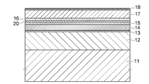
図3は、図1に示す発光素子1におけるp型GaN層15、中間層20、およびn型GaN層16が積層された部分の他の実施形態を示す模式拡大断面図である。
図5は、図3に示す積層部の模式的なエネルギーバンド図である。
FIG. 3 is a schematic enlarged cross-sectional view showing another embodiment of the laminated portion of the p-
FIG. 5 is a schematic energy band diagram of the laminated portion shown in FIG.
この例では、中間層20は、ノンドープGaN層21と、ノンドープInGaN層22とを有する。ノンドープInGaN層22は、n型GaN層16とノンドープGaN層21との間に設けられている。ノンドープGaN層21は、ノンドープInGaN層22とp型GaN層15との間に設けられている。
In this example,
ノンドープGaN層21の厚さは、ノンドープInGaN層22の厚さよりも厚い。ノンドープGaN層21の厚さ、およびノンドープInGaN層22の厚さを合計した厚さ、すなわち中間層20の厚さは、p型GaN層15とn型GaN層16とが形成する空乏層の幅以下である。
The
ノンドープGaN層21の厚さは3nm以上5nm以下であり、ノンドープInGaN層22の厚さは3nm以上5nm以下である。
The thickness of the
p型GaN層15とn型GaN層16との間に、ノンドープGaN層21よりもバンドギャップが小さいノンドープInGaN層22が設けられる。そのため、ノンドープGaN層21のみを中間層20として設けた図4の構造に比べて、図5に示すように、p型GaN層15の価電子帯の電子eがn型GaN層16の伝導帯にトンネリングする際の障壁となる空乏層幅を狭くすることができる。このため、図5に示すノンドープGaN層21と、ノンドープInGaN層22とを有する中間層20によれば、図4の構造よりもトンネル効果が生じやすく、駆動電圧の低減が可能となる。
A
InGaNはGaNよりも結晶性が悪くなる傾向があるため、ノンドープGaN層21の厚さは、ノンドープInGaN層22の厚さよりも厚いことが好ましい。
Since InGaN tends to be less crystalline than GaN, the
ノンドープGaN層21よりも結晶性が悪くなる傾向があるノンドープInGaN層22を先にp型GaN層15上に形成すると、そのノンドープInGaN層22上に形成されるノンドープGaN層21にもノンドープInGaN層22の結晶性が引き継がれやすくなる。そのため、p型GaN層15上に先にノンドープGaN層21を形成し、そのノンドープGaN層21上にノンドープInGaN層22を形成することが好ましい。このような構成とすることで、n型GaN層16が形成される下地となる層の結晶性の悪化を、ノンドープInGaN層22を形成した後、ノンドープGaN層21を形成する場合に比べて低減することができる。
If the
図16は、本発明の実施形態の発光素子1を用いた発光装置の一例を示す図である。
FIG. 16 is a diagram showing an example of a light-emitting device using the light-emitting
前述した実施形態の発光素子1は、実装基板100上に形成された配線電極等に実装される。発光素子1の基板11と実装基板100との間に半導体積層体10が設けられている。基板11上には波長変換部材101が設けられている。波長変換部材101には、例えば、蛍光体が含有された焼結体等を用いることができる。発光素子1及び波長変換部材101の側面を覆うように光反射性を有する樹脂層102が形成されている。発光素子1の側面には第1の発光層13と第2の発光層18が露出しており、第1の発光層13および第2の発光層18の側面が樹脂層102により覆われている。樹脂層102には、光反射性を有する粒子が含有されている。このような粒子としては、酸化アルミニウムや酸化チタン等を用いることができる。発光素子1からの光は主に樹脂層102から露出した波長変換部材101の上面側から取り出される。
The light-emitting
本発明の実施形態の発光素子1は、半導体積層体10に第1の発光層13と第2の発光層18の2つの発光層を有しているため、発光層が1つである発光素子に比べて単位面積当たりの出力を高くすることできる。したがって、本発明の実施形態の発光素子1を用いることで、単位面積あたりの出力が高い発光装置とすることができる。
Since the light-emitting
なお、上述した実施形態においては、n型GaN層16をn型の不純物がドープされたGaN層として説明したが、GaN層に代えて、本発明の効果を奏する程度に微量のInやAlが含有されたInGaN層やAlGaN層とすることもできる。また、上述した実施形態においては、p型GaN層15をp型の不純物がドープされたGaN層として説明したが、GaN層に代えて、本発明の効果を奏する程度に微量のInやAlが含有されたInGaN層やAlGaN層とすることもできる。ここで、GaN層に微量のInやAlが含有されるとは、GaN層に対してInやAlが0.1%以下の混晶比で含有されることを意味する。
In the above-described embodiment, the n-
以上、具体例を参照しつつ、本発明の実施形態及び実施例について説明した。しかし、本発明は、これらの具体例に限定されるものではない。本発明の上述した実施形態を基にして、当業者が適宜設計変更して実施し得る全ての形態も、本発明の要旨を包含する限り、本発明の範囲に属する。その他、本発明の思想の範疇において、当業者であれば、各種の変更例及び修正例に想到し得るものであり、それら変更例及び修正例についても本発明の範囲に属するものと了解される。 The embodiments and examples of the present invention have been described above with reference to specific examples. However, the invention is not limited to these specific examples. Based on the above-described embodiment of the present invention, all forms that can be implemented by those skilled in the art by appropriately designing and changing are also included in the scope of the present invention as long as they include the gist of the present invention. In addition, within the scope of the idea of the present invention, those skilled in the art can conceive of various modifications and modifications, and it is understood that these modifications and modifications also belong to the scope of the present invention. .
1…発光素子、10…半導体積層体、11…基板、12…第1のn型窒化物半導体層、13…第1の発光層、14…第1のp型窒化物半導体層、15…p型GaN層、16…n型GaN層、17…第2のn型窒化物半導体層、18…第2の発光層、19…第2のp型窒化物半導体層、20…中間層、21…ノンドープGaN層、22…ノンドープInGaN層、41…n側電極、42…p側電極、100…実装基板、101…波長変換部材、102…樹脂層
DESCRIPTION OF
Claims (6)
前記第1のn型窒化物半導体層上に設けられた第1の発光層と、
前記第1の発光層上に設けられ、p型不純物がドープされたp型GaN層と、
前記p型GaN層上に設けられ、前記第1のn型窒化物半導体層よりも高い不純物濃度のn型不純物がドープされたn型GaN層と、
前記p型GaN層と前記n型GaN層との間に設けられ、厚さが3nm以上5nm以下であるノンドープGaN層と、
前記ノンドープGaN層と前記n型GaN層との間に設けられたノンドープInGaN層と、
前記n型GaN層上に設けられ、n型不純物がドープされた第2のn型窒化物半導体層と、
前記第2のn型窒化物半導体層上に設けられた第2の発光層と、
前記第2の発光層上に設けられ、p型不純物がドープされたp型窒化物半導体層と、
を備え、
前記p型GaN層と前記n型GaN層とによりトンネル接合が形成される発光素子。 a first n-type nitride semiconductor layer doped with an n-type impurity;
a first light emitting layer provided on the first n-type nitride semiconductor layer;
a p-type GaN layer provided on the first light-emitting layer and doped with a p-type impurity;
an n-type GaN layer provided on the p-type GaN layer and doped with an n-type impurity having an impurity concentration higher than that of the first n-type nitride semiconductor layer;
a non-doped GaN layer provided between the p-type GaN layer and the n-type GaN layer and having a thickness of 3 nm or more and 5 nm or less;
a non-doped InGaN layer provided between the non-doped GaN layer and the n-type GaN layer;
a second n-type nitride semiconductor layer provided on the n-type GaN layer and doped with an n-type impurity;
a second light emitting layer provided on the second n-type nitride semiconductor layer;
a p-type nitride semiconductor layer provided on the second light-emitting layer and doped with a p-type impurity;
with
A light-emitting device in which a tunnel junction is formed by the p-type GaN layer and the n-type GaN layer.
前記第1のn型窒化物半導体層上に、第1の発光層を形成する工程と、
前記第1の発光層上に、p型不純物がドープされたp型GaN層を形成する工程と、
前記p型GaN層上に、厚さが3nm以上5nm以下であるノンドープGaN層と、前記ノンドープGaN層上に設けられたノンドープInGaN層とを含む中間層を形成する工程と、
前記中間層上に、前記第1のn型窒化物半導体層よりも高い不純物濃度のn型不純物がドープされたn型GaN層を形成する工程と、
前記n型GaN層上に、n型不純物がドープされた第2のn型窒化物半導体層を形成する工程と、
前記第2のn型窒化物半導体層上に、第2の発光層を形成する工程と、
前記第2の発光層上に、p型不純物がドープされたp型窒化物半導体層を形成する工程と、
を備え、
前記p型GaN層と前記n型GaN層とによりトンネル接合が形成される、発光素子の製造方法。 forming a first n-type nitride semiconductor layer doped with an n-type impurity;
forming a first light-emitting layer on the first n-type nitride semiconductor layer;
forming a p-type impurity-doped p-type GaN layer on the first light-emitting layer;
forming on the p-type GaN layer an intermediate layer including a non-doped GaN layer having a thickness of 3 nm or more and 5 nm or less and a non -doped InGaN layer provided on the non-doped GaN layer ;
forming, on the intermediate layer, an n-type GaN layer doped with n-type impurities having an impurity concentration higher than that of the first n-type nitride semiconductor layer;
forming a second n-type nitride semiconductor layer doped with an n-type impurity on the n-type GaN layer;
forming a second light-emitting layer on the second n-type nitride semiconductor layer;
forming a p-type nitride semiconductor layer doped with a p-type impurity on the second light emitting layer;
with
A method of manufacturing a light-emitting device, wherein a tunnel junction is formed by the p-type GaN layer and the n-type GaN layer.
Priority Applications (1)
| Application Number | Priority Date | Filing Date | Title |
|---|---|---|---|
| US16/844,167 US11538962B2 (en) | 2019-04-23 | 2020-04-09 | Light-emitting element and method for manufacturing light-emitting element |
Applications Claiming Priority (2)
| Application Number | Priority Date | Filing Date | Title |
|---|---|---|---|
| JP2019081497 | 2019-04-23 | ||
| JP2019081497 | 2019-04-23 |
Publications (2)
| Publication Number | Publication Date |
|---|---|
| JP2020181976A JP2020181976A (en) | 2020-11-05 |
| JP7129630B2 true JP7129630B2 (en) | 2022-09-02 |
Family
ID=73024867
Family Applications (1)
| Application Number | Title | Priority Date | Filing Date |
|---|---|---|---|
| JP2020050778A Active JP7129630B2 (en) | 2019-04-23 | 2020-03-23 | Light-emitting element and method for manufacturing light-emitting element |
Country Status (1)
| Country | Link |
|---|---|
| JP (1) | JP7129630B2 (en) |
Families Citing this family (1)
| Publication number | Priority date | Publication date | Assignee | Title |
|---|---|---|---|---|
| CN114335273B (en) * | 2021-12-30 | 2023-09-01 | 淮安澳洋顺昌光电技术有限公司 | LED epitaxial wafer, preparation method thereof and LED chip |
Citations (9)
| Publication number | Priority date | Publication date | Assignee | Title |
|---|---|---|---|---|
| JP2004128502A (en) | 2002-09-30 | 2004-04-22 | Lumileds Lighting Us Llc | Light emitting device including tunnel junction |
| JP2007520071A (en) | 2004-01-29 | 2007-07-19 | エルヴェーエー・スペース・ソーラー・パワー・ゲーエムベーハー | Semiconductor structure with active region |
| JP2008078297A (en) | 2006-09-20 | 2008-04-03 | Mitsubishi Cable Ind Ltd | GaN-BASED SEMICONDUCTOR LIGHT-EMITTING DEVICE |
| JP2009521814A (en) | 2005-12-27 | 2009-06-04 | サムスン エレクトロニクス カンパニー リミテッド | Group III nitride light emitting device |
| JP2010532926A (en) | 2007-07-09 | 2010-10-14 | オスラム オプト セミコンダクターズ ゲゼルシャフト ミット ベシュレンクテル ハフツング | Radiation emitting semiconductor body |
| JP2013021334A (en) | 2011-07-12 | 2013-01-31 | Samsung Electronics Co Ltd | Nitride light-emitting element |
| US20130270514A1 (en) | 2012-04-16 | 2013-10-17 | Adam William Saxler | Low resistance bidirectional junctions in wide bandgap semiconductor materials |
| JP2017157667A (en) | 2016-03-01 | 2017-09-07 | 学校法人 名城大学 | Nitride semiconductor light-emitting device |
| WO2018081635A1 (en) | 2016-10-28 | 2018-05-03 | Lumileds Llc | Methods for growing light emitting devices under ultra-violet illumination |
Family Cites Families (1)
| Publication number | Priority date | Publication date | Assignee | Title |
|---|---|---|---|---|
| JPH0992847A (en) * | 1995-09-21 | 1997-04-04 | Hitachi Cable Ltd | Tunnel semiconductor device |
-
2020
- 2020-03-23 JP JP2020050778A patent/JP7129630B2/en active Active
Patent Citations (9)
| Publication number | Priority date | Publication date | Assignee | Title |
|---|---|---|---|---|
| JP2004128502A (en) | 2002-09-30 | 2004-04-22 | Lumileds Lighting Us Llc | Light emitting device including tunnel junction |
| JP2007520071A (en) | 2004-01-29 | 2007-07-19 | エルヴェーエー・スペース・ソーラー・パワー・ゲーエムベーハー | Semiconductor structure with active region |
| JP2009521814A (en) | 2005-12-27 | 2009-06-04 | サムスン エレクトロニクス カンパニー リミテッド | Group III nitride light emitting device |
| JP2008078297A (en) | 2006-09-20 | 2008-04-03 | Mitsubishi Cable Ind Ltd | GaN-BASED SEMICONDUCTOR LIGHT-EMITTING DEVICE |
| JP2010532926A (en) | 2007-07-09 | 2010-10-14 | オスラム オプト セミコンダクターズ ゲゼルシャフト ミット ベシュレンクテル ハフツング | Radiation emitting semiconductor body |
| JP2013021334A (en) | 2011-07-12 | 2013-01-31 | Samsung Electronics Co Ltd | Nitride light-emitting element |
| US20130270514A1 (en) | 2012-04-16 | 2013-10-17 | Adam William Saxler | Low resistance bidirectional junctions in wide bandgap semiconductor materials |
| JP2017157667A (en) | 2016-03-01 | 2017-09-07 | 学校法人 名城大学 | Nitride semiconductor light-emitting device |
| WO2018081635A1 (en) | 2016-10-28 | 2018-05-03 | Lumileds Llc | Methods for growing light emitting devices under ultra-violet illumination |
Non-Patent Citations (2)
| Title |
|---|
| CHANG, S.J. et al.,Cascaded GaN Light-Emitting Diodes With Hybrid Tunnel Junction Layers,IEEE JOURNAL OF QUANTUM ELECTRONICS,米国,IEEE,2015年06月15日,VOL.51, NO.8,p.3300505 |
| CHANG, S.J. et al.,GaN-Based Multiquantum Well Light-Emitting Diodes With Tunnel-Junction-Cascaded Active Regions,IEEE ELECTRON DEVICE LETTERS,米国,IEEE,2015年01月28日,VOL.36, NO.4,pp.366-368 |
Also Published As
| Publication number | Publication date |
|---|---|
| JP2020181976A (en) | 2020-11-05 |
Similar Documents
| Publication | Publication Date | Title |
|---|---|---|
| JP5143171B2 (en) | Semiconductor light emitting device and manufacturing method thereof | |
| JP4954536B2 (en) | Nitride semiconductor light emitting device | |
| JP4881491B2 (en) | Semiconductor light emitting device | |
| JP7101347B2 (en) | Manufacturing method of light emitting element | |
| US11538962B2 (en) | Light-emitting element and method for manufacturing light-emitting element | |
| US20100181583A1 (en) | Radiation-emitting semiconductor chip | |
| JP2016513878A (en) | Monolithic light emitting device | |
| JP4960465B2 (en) | Semiconductor light emitting device | |
| JP3940933B2 (en) | Nitride semiconductor device | |
| JP7129630B2 (en) | Light-emitting element and method for manufacturing light-emitting element | |
| JP5762901B2 (en) | Semiconductor light emitting device, wafer, method for manufacturing semiconductor light emitting device, and method for manufacturing wafer | |
| JP4292925B2 (en) | Method for manufacturing group III nitride compound semiconductor light emitting device | |
| JP5948767B2 (en) | Nitride semiconductor light emitting device | |
| JP7149486B2 (en) | Method for manufacturing light-emitting element | |
| JP2005150645A (en) | Light-emitting element | |
| JP5135465B2 (en) | Semiconductor light emitting device and manufacturing method thereof | |
| JP6192722B2 (en) | Optoelectronic semiconductor body and optoelectronic semiconductor chip | |
| JP7385138B2 (en) | Manufacturing method of light emitting device | |
| JP7333504B2 (en) | light emitting element | |
| JP7481618B2 (en) | Method for manufacturing nitride semiconductor device | |
| JP6670401B2 (en) | Semiconductor laminate | |
| JP5458162B2 (en) | Semiconductor light emitting device | |
| JP2007201146A (en) | Light emitting element and its manufacturing method | |
| JP5364818B2 (en) | Semiconductor light emitting device and manufacturing method thereof | |
| CN117015860A (en) | Light-emitting element |
Legal Events
| Date | Code | Title | Description |
|---|---|---|---|
| A621 | Written request for application examination |
Free format text: JAPANESE INTERMEDIATE CODE: A621 Effective date: 20200827 |
|
| A977 | Report on retrieval |
Free format text: JAPANESE INTERMEDIATE CODE: A971007 Effective date: 20210831 |
|
| A131 | Notification of reasons for refusal |
Free format text: JAPANESE INTERMEDIATE CODE: A131 Effective date: 20210907 |
|
| A521 | Request for written amendment filed |
Free format text: JAPANESE INTERMEDIATE CODE: A523 Effective date: 20211014 |
|
| A131 | Notification of reasons for refusal |
Free format text: JAPANESE INTERMEDIATE CODE: A131 Effective date: 20220325 |
|
| A521 | Request for written amendment filed |
Free format text: JAPANESE INTERMEDIATE CODE: A523 Effective date: 20220421 |
|
| TRDD | Decision of grant or rejection written | ||
| A01 | Written decision to grant a patent or to grant a registration (utility model) |
Free format text: JAPANESE INTERMEDIATE CODE: A01 Effective date: 20220722 |
|
| A61 | First payment of annual fees (during grant procedure) |
Free format text: JAPANESE INTERMEDIATE CODE: A61 Effective date: 20220804 |
|
| R151 | Written notification of patent or utility model registration |
Ref document number: 7129630 Country of ref document: JP Free format text: JAPANESE INTERMEDIATE CODE: R151 |