JP7127040B2 - pressure sensitive stylus - Google Patents
pressure sensitive stylus Download PDFInfo
- Publication number
- JP7127040B2 JP7127040B2 JP2019541136A JP2019541136A JP7127040B2 JP 7127040 B2 JP7127040 B2 JP 7127040B2 JP 2019541136 A JP2019541136 A JP 2019541136A JP 2019541136 A JP2019541136 A JP 2019541136A JP 7127040 B2 JP7127040 B2 JP 7127040B2
- Authority
- JP
- Japan
- Prior art keywords
- tip
- housing
- writing tip
- stylus
- pressure sensor
- Prior art date
- Legal status (The legal status is an assumption and is not a legal conclusion. Google has not performed a legal analysis and makes no representation as to the accuracy of the status listed.)
- Active
Links
Images


Classifications
-
- G—PHYSICS
- G06—COMPUTING OR CALCULATING; COUNTING
- G06F—ELECTRIC DIGITAL DATA PROCESSING
- G06F3/00—Input arrangements for transferring data to be processed into a form capable of being handled by the computer; Output arrangements for transferring data from processing unit to output unit, e.g. interface arrangements
- G06F3/01—Input arrangements or combined input and output arrangements for interaction between user and computer
- G06F3/03—Arrangements for converting the position or the displacement of a member into a coded form
- G06F3/033—Pointing devices displaced or positioned by the user, e.g. mice, trackballs, pens or joysticks; Accessories therefor
- G06F3/0354—Pointing devices displaced or positioned by the user, e.g. mice, trackballs, pens or joysticks; Accessories therefor with detection of two-dimensional [2D] relative movements between the device, or an operating part thereof, and a plane or surface, e.g. 2D mice, trackballs, pens or pucks
- G06F3/03545—Pens or stylus
-
- G—PHYSICS
- G06—COMPUTING OR CALCULATING; COUNTING
- G06F—ELECTRIC DIGITAL DATA PROCESSING
- G06F3/00—Input arrangements for transferring data to be processed into a form capable of being handled by the computer; Output arrangements for transferring data from processing unit to output unit, e.g. interface arrangements
- G06F3/01—Input arrangements or combined input and output arrangements for interaction between user and computer
- G06F3/03—Arrangements for converting the position or the displacement of a member into a coded form
- G06F3/033—Pointing devices displaced or positioned by the user, e.g. mice, trackballs, pens or joysticks; Accessories therefor
- G06F3/038—Control and interface arrangements therefor, e.g. drivers or device-embedded control circuitry
- G06F3/0383—Signal control means within the pointing device
-
- G—PHYSICS
- G06—COMPUTING OR CALCULATING; COUNTING
- G06F—ELECTRIC DIGITAL DATA PROCESSING
- G06F3/00—Input arrangements for transferring data to be processed into a form capable of being handled by the computer; Output arrangements for transferring data from processing unit to output unit, e.g. interface arrangements
- G06F3/01—Input arrangements or combined input and output arrangements for interaction between user and computer
- G06F3/03—Arrangements for converting the position or the displacement of a member into a coded form
- G06F3/041—Digitisers, e.g. for touch screens or touch pads, characterised by the transducing means
-
- G—PHYSICS
- G06—COMPUTING OR CALCULATING; COUNTING
- G06F—ELECTRIC DIGITAL DATA PROCESSING
- G06F2203/00—Indexing scheme relating to G06F3/00 - G06F3/048
- G06F2203/041—Indexing scheme relating to G06F3/041 - G06F3/045
- G06F2203/04101—2.5D-digitiser, i.e. digitiser detecting the X/Y position of the input means, finger or stylus, also when it does not touch, but is proximate to the digitiser's interaction surface and also measures the distance of the input means within a short range in the Z direction, possibly with a separate measurement setup
-
- G—PHYSICS
- G06—COMPUTING OR CALCULATING; COUNTING
- G06F—ELECTRIC DIGITAL DATA PROCESSING
- G06F2203/00—Indexing scheme relating to G06F3/00 - G06F3/048
- G06F2203/041—Indexing scheme relating to G06F3/041 - G06F3/045
- G06F2203/04105—Pressure sensors for measuring the pressure or force exerted on the touch surface without providing the touch position
-
- G—PHYSICS
- G06—COMPUTING OR CALCULATING; COUNTING
- G06F—ELECTRIC DIGITAL DATA PROCESSING
- G06F2203/00—Indexing scheme relating to G06F3/00 - G06F3/048
- G06F2203/041—Indexing scheme relating to G06F3/041 - G06F3/045
- G06F2203/04108—Touchless 2D- digitiser, i.e. digitiser detecting the X/Y position of the input means, finger or stylus, also when it does not touch, but is proximate to the digitiser's interaction surface without distance measurement in the Z direction
Landscapes
- Engineering & Computer Science (AREA)
- General Engineering & Computer Science (AREA)
- Theoretical Computer Science (AREA)
- Human Computer Interaction (AREA)
- Physics & Mathematics (AREA)
- General Physics & Mathematics (AREA)
- Pens And Brushes (AREA)
- Position Input By Displaying (AREA)
- Force Measurement Appropriate To Specific Purposes (AREA)
- Measurement Of Length, Angles, Or The Like Using Electric Or Magnetic Means (AREA)
Description
スタイラスは、コンピューティングデバイスとともに使用するために当技術分野で公知である。スタイラスの位置検出は、コンピューティングデバイスに関連付けられるデジタイザセンサに入力を提供し、ユーザコマンドとして解釈され得る。位置検出は、スタイラスのチップがデジタイザセンサの検出面上に接触しているか、かつ/又はホバリングしている間に行われ得る。デジタイザセンサは、電子ディスプレイ画面内に一体化されることが多く、コンピューティングデバイスは、スタイラスの位置を画面上に描かれる情報と相関させる。 Styluses are known in the art for use with computing devices. The position detection of the stylus provides input to a digitizer sensor associated with the computing device and can be interpreted as user commands. Position sensing may occur while the tip of the stylus is touching and/or hovering over the sensing surface of the digitizer sensor. Digitizer sensors are often integrated into electronic display screens, and computing devices correlate stylus position with information drawn on the screen.
一部のスタイラスは、ユーザがスタイラスを使用している間にスタイラスのチップに加えられる圧力のレベルを感知し、任意に報告するという点で、感圧性である。コンピューティングデバイス上で実行されるアプリケーションは、その後、この情報を使用することができる。例えばグラフィックアプリケーションは、検出された圧力レベルに基づいて、引く線の線太さ又は影を調整することができる。 Some styluses are pressure sensitive in that they sense and optionally report the level of pressure applied to the tip of the stylus while the user is using the stylus. Applications running on the computing device can then use this information. For example, the graphics application may adjust the line thickness or shadow of the drawn line based on the detected pressure level.
本開示は、デバイスの相互作用チップ(interacting tip)に加えられる圧力を感知するセンサを含むハンドヘルドデバイスに関する。ハンドヘルドデバイスは、例えばスタイラスであってよい。本開示の実施形態によれば、センサは、低コストで実装されることができ、比較的単純な構造を有し、そして改善された感度及び精度を提供することができる、改善された容量ベースの圧力センサである。 The present disclosure relates to handheld devices that include sensors that sense pressure applied to an interacting tip of the device. A handheld device may be, for example, a stylus. According to embodiments of the present disclosure, the sensor can be implemented at low cost, has a relatively simple structure, and can provide improved sensitivity and accuracy. pressure sensor.
別段の定めがない限り、本明細書で使用されるすべての技術的及び/又は科学的用語は、当業者によって一般的に理解されるものと同じ意味を有する。本明細書で説明されるものと同様又は等価な方法及び材料を、本開示の実施形態の実施又は試験において使用することができるが、例示的な方法及び/又は材料は、以下で説明される。矛盾がある場合は、定義を含む本特許明細書が支配することになる。加えて、材料、方法、及び実施例は、例示にすぎず、必ずしも限定するように意図されていない。 Unless defined otherwise, all technical and/or scientific terms used herein have the same meaning as commonly understood by one of ordinary skill in the art. Although methods and materials similar or equivalent to those described herein can be used in the practice or testing of the embodiments of the present disclosure, exemplary methods and/or materials are described below. . In case of conflict, the patent specification, including definitions, will control. In addition, the materials, methods, and examples are illustrative only and not necessarily intended to be limiting.
本開示のいくつかの実装は、添付の図面に関連して、単なる例示として本明細書で説明される。次に図面を詳細に参照するが、図示される詳細は、例示として、本開示の実施の例示的な議論のためのものであることが強調される。この点に関し、図面を伴う本説明は、本開示の実施がどのように実施され得るかを当業者に明らかにする。 Several implementations of the disclosure are described herein, by way of example only, in connection with the accompanying drawings. Referring now in detail to the drawings, it is emphasized that the details shown are for purposes of exemplary discussion of the practice of the present disclosure, by way of illustration. In this regard, the description, along with the drawings, will make it clear to those skilled in the art how the practice of the disclosure can be implemented.
図面は次のとおりである。 The drawings are as follows.
デバイスのハウジングに対して移動可能な相互作用チップを有するハンドヘルドデバイスは、ユーザがデバイスを操作している間にチップに加えられる圧力を感知するための容量ベースの圧力センサを含む。いくつかの例示の実装によると、センサは、相互作用チップに固定される剛性要素と、ハウジングに固定されるエラストマと、それらの間の容量結合を検出するための回路とを含む。剛性要素及びエラストマは、相互作用チップに圧力が加えられると、剛性要素がエラストマの方へ動いてエラストマを押しつけるように、ハウジング内に配置される。剛性要素及びエラストマの双方が導電性である。いくつかの例示の実装では、剛性要素は、該剛性要素とエラストマとの間に誘電体分離を提供する電気的絶縁材料でコーティングされる。あるいはまた、エラストマは、誘電体分離を提供する電気的絶縁材料でコーティングされてもよい。チップに加えられる圧力は、検出される容量結合のレベルに基づいて感知され得る。 A handheld device having an interactive tip that is movable relative to the housing of the device includes a capacitance-based pressure sensor for sensing pressure applied to the tip while the user is manipulating the device. According to some example implementations, the sensor includes a rigid element fixed to the interaction chip, an elastomer fixed to the housing, and circuitry for detecting capacitive coupling therebetween. The rigid element and elastomer are arranged within the housing such that when pressure is applied to the interaction tip, the rigid element moves toward and presses against the elastomer. Both the rigid element and the elastomer are electrically conductive. In some example implementations, the rigid elements are coated with an electrically insulating material that provides dielectric isolation between the rigid elements and the elastomer. Alternatively, the elastomer may be coated with an electrically insulating material that provides dielectric isolation. Pressure applied to the tip can be sensed based on the level of capacitive coupling detected.
任意で、剛性要素は、チップ又はチップホルダの一端に形成され、相互作用チップ又はチップを保持するチップホルダ、例えば単一部品として形成されるチップホルダと一体である。剛性要素をデバイス内の既存の部品と一体化することにより、材料表(bill of material)を低減することができ、接続部品に関連する公差をなくすことができ、そして部品間の解放に起因するいかなる誤作動も回避することができる。剛性要素を既存の部品と一体化する際の別の利点は、圧力センサを組み込むのに必要なスペースを減らすことができることである。 Optionally, the rigid element is formed at one end of the chip or chip holder and is integral with the chip holder holding the interacting chip or chip, eg formed as a single piece. By integrating the rigid elements with existing parts in the device, the bill of material can be reduced, tolerances associated with connecting parts can be eliminated, and release between parts can result in Any malfunction can be avoided. Another advantage in integrating rigid elements with existing parts is the reduction in space required to incorporate the pressure sensor.
典型的には、剛性要素及びエラストマのうちの一方は、要素の間の有効接触面積が圧力に応じて変化し得るように、ドーム形状、円錐形、あるいは他の平らではない形状である。これは、剛性要素とエラストマとの間の近接性及び接触面積の双方が、検出される容量結合に影響を及ぼす可能性があるので、圧力が検出され得る分解能を改善することができる。 Typically, one of the rigid element and the elastomer is dome-shaped, conical, or otherwise non-planar so that the effective contact area between the elements can vary with pressure. This can improve the resolution with which pressure can be detected, as both the proximity and contact area between the rigid element and the elastomer can affect the capacitive coupling detected.
いくつかの実装では、剛性要素の形状は、所望の力曲線、例えば検出された容量結合とチップに加えられた圧力との間の所望の関係を提供する。剛性要素を用いて所望の形状を形成し、平らなエラストマを使用する利点は、剛性要素の材料、例えば金属又は導電性プラスチックの材料が、エラストマよりも低い公差で成形され得ることである。設計の単純さ及び部品の低い公差により、所望の力曲線は、経時的にかつ温度範囲にわたって一貫性があり得る。剛性要素がチップ又はチップホルダに一体化される実装では、剛性要素を規定された形状へ成形することは、コストを増加させず、必要な形状でエラストマを製造する必要性を排除する可能性が高い。剛性要素によって所望の形状が提供されると、市販の製品から平らなエラストマを選択することができる。 In some implementations, the shape of the rigid element provides a desired force curve, eg, a desired relationship between sensed capacitive coupling and pressure applied to the tip. An advantage of using a rigid element to form the desired shape and using a flat elastomer is that the material of the rigid element, such as metal or conductive plastic, can be molded to lower tolerances than the elastomer. Due to the simplicity of the design and the low tolerances of the parts, the desired force curve can be consistent over time and temperature range. In implementations where the rigid element is integrated into the chip or chip holder, molding the rigid element into a defined shape does not add cost and may eliminate the need to manufacture the elastomer in the required shape. high. Once the desired shape is provided by the rigid elements, flat elastomers can be selected from commercial products.
いくつかの実装では、センサの感度は、剛性要素上の10nm規模(order of magnitude)~10μm規模、例えば20μm未満の範囲の薄い非導電性コーティング層でセンサを動作させることによって改善される。非導電性コーティングの誘電率定数は、所望の特性を有する誘電体又は非導電層を提供するように選択され得る。 In some implementations, the sensitivity of the sensor is improved by operating the sensor with a thin non-conductive coating layer in the order of magnitude to 10 μm scale, eg, less than 20 μm, on the rigid element. The dielectric constant of the non-conductive coating can be selected to provide a dielectric or non-conductive layer with desired properties.
誘電体層が剛性要素に塗布されるコーティングである実装においては、厚さは、標準的な製造方法を使用して、例えば陽極酸化製造プロセスを使用して、低い公差を有する所望の厚さに、制御可能に制限することができる。層の厚さを制御することによって、センサの精度を改善することができ、センサ間の製造性のばらつきを低減することができる。これは、各センサを較正する必要性をなくすことができる。この実装は、より厚く、かつ、その厚さ並びにより高いコストに関してより高い公差に関連付けられるプリント回路基板の層を誘電体層として使用する既知の方法よりも有利である。いくつかの例では、規定されたテクスチャをコーティング又はコーティングの一部に適用して、接触中のコーティングとエラストマとの間の接着を減少させる。また、テクスチャは、標準的な製造方法によるコーティングの間に比較的低コストで適用され得る。テクスチャを加えるための任意の製造方法は、例えば吹付け加工(abrasive blasting)又は腐食(erosion)を含んでもよい。 In implementations where the dielectric layer is a coating applied to the rigid element, the thickness is adjusted to the desired thickness with low tolerances using standard manufacturing methods, such as an anodizing manufacturing process. , can be controllably limited. By controlling the thickness of the layers, sensor accuracy can be improved and manufacturability variability between sensors can be reduced. This can eliminate the need to calibrate each sensor. This implementation is advantageous over the known method of using printed circuit board layers as dielectric layers which are thicker and associated with higher tolerances in terms of their thickness as well as higher cost. In some examples, a defined texture is applied to the coating or portions of the coating to reduce adhesion between the coating and the elastomer during contact. Also, the texture can be applied at relatively low cost during coating by standard manufacturing methods. Any manufacturing method for adding texture may include, for example, abrasive blasting or erosion.
次に、図1を参照すると、例示の感圧スタイラスの簡略化されたブロック図が図示されている。いくつかの実装では、スタイラス100は、電源105、1つ以上のプリント回路基板(PCB)アセンブリ120及び125、1つ以上のユーザ制御ボタン130、書込みチップ150、書込みチップ150に関連する圧力センサ200及び任意のコンポーネント115、例えば追加のセンサを収容する、ハウジング110を含む。電源105は、1つ以上の再充電可能バッテリ及び/又はスーパーキャパシタを含んでもよい。PCBアセンブリ120は、スタイラス100の動作を制御するASIC121を含んでもよい。スタイラス100の動作中、ASIC121は信号を生成することができ、この信号は、書込みチップ150を介して、あるいは書込みチップ150に関連付けられるチップホルダ155を介して送信されてよい。
Referring now to FIG. 1, a simplified block diagram of an exemplary pressure sensitive stylus is depicted. In some implementations,
書込みチップ150は、典型的に、端部151に加えられる接触圧力に応答して、ハウジング110内へ及びハウジング110の外へスライドするように構成される。コイルバネのような弾性要素160が、ハウジング110及び書込みチップ150に結合されて、書込みチップ150の動きに対して弾性力を提供することができる。いくつかの実装では、書込みチップ150はチップホルダ155に固定、例えば圧入され、チップホルダ155は、弾性要素160に機械的に結合される。書込みチップ150の移動範囲は、10μm規模、例えば0~80μmであってよい。
Writing
圧力センサ200は、キャパシタの第1電極として剛性要素220を含み、キャパシタの第2電極としてエラストマ210を含む容量ベースのセンサであってよい。圧力センサ200によって検出される圧力は、剛性要素220とエラストマ210との間の容量結合に関連する。剛性要素220は、書込みチップ150に固定されてよく、書込みチップ150の端部151に接触圧力が加えられると、エラストマ210を押しつけることができる。剛性要素220及びエラストマ210の双方が導電性材料から形成されてよい。いくつかの例示的な実装では、剛性要素220は、物理的接触の間に電気的絶縁を提供する絶縁材料の層225、例えば剛性要素220とエラストマ210との間の誘電体層でコーティングされる。
いくつかの例示の実装では、エラストマ210は、PCB125に取り付けられる平らな要素である。エラストマ210を有するPCB125は、エラストマ210が、例えばスタイラス100の長手軸101に略垂直な角度で剛性要素220に対向するように、ハウジング110に固定されてよい。いくつかの実装では、剛性要素220が、増大した圧力でエラストマ210と係合するにつれて、剛性要素220とエラストマ210との間の表面接触が変化し得るように、剛性要素220は、ドーム形状、円錐形、あるいは他の平らでない形状とすることができる。剛性要素220は、チップホルダ155の延長部であってもよく、同じ材料、例えば金属又は導電性プラスチックから形成されてよい。
In some example implementations,
エラストマ210は、PCB120及び電源105に電気的に接続される。いくつかの実装では、ASIC121は、圧力センサ200の動作のために、剛性要素220及びエラストマ210の少なくとも一方を充電するように制御する。圧力センサ200は、剛性要素220とエラストマ210との間の容量結合を検出する容量測定ユニットを更に含む。容量測定ユニットは、ASIC121に埋め込まれてもよい。任意で、容量測定ユニットは、市販のユニット、例えば電荷増幅器である。
圧力センサ200からの出力は、例えばASIC121によってデジタル的に符号化され、スタイラス100によって送信される信号を変調するために使用される。信号は、圧力センサ200から取得された情報、並びにボタン130の状態、スタイラスID、バッテリの健全性状態、スタイラス内に埋め込まれるかスタイラスと通信する他のセンサからの情報及び/又は他の情報を含むように変調され得る。いくつかの例示的な実装では、送信される情報は圧力レベルである。任意で、送信される情報は、圧力センサ200によって検出されるホバリング又はタッチ状態の一方である。
The output from
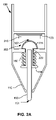
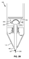
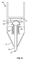
ここで、図2A及び図2Bを参照すると、図2A及び図2Bは、スタイラスに一体化され得る例示の圧力センサの要素の簡略化された概略図を示しており、センサは、それぞれ、ニュートラルの状態及び押圧状態で示されている。圧力センサ200は、剛性要素220とエラストマ210との間の容量結合のレベルをモニタする。いくつかの実装では、ホバリング中、例えば接触力が書込みチップ150の端部151に加えられていない間は、規定されたエアギャップ157が、剛性要素220をエラストマ210から分離する(図2A)。エアギャップ157は、弾性要素160によって加えられる予荷重(preloading force)によって維持され得る。
Reference is now made to FIGS. 2A and 2B, which show simplified schematic diagrams of elements of an exemplary pressure sensor that may be integrated into a stylus, the sensors each having a neutral state and pressed state.
端部151に加えられた接触力250が弾性要素160の予荷重に打ち勝つと、書込みチップ150はチップホルダ155及び剛性要素220とともにエラストマ210の方へ動く。剛性要素220がエラストマ210に近づくにつれて、エアギャップ157は減少し、容量結合が増加する。力250が除去されると、弾性要素160によって加えられる弾性力がエアギャップ157を回復し得る。
When
力250が増加するにつれて、剛性要素220はエラストマ210に押しつけられてエラストマ210を変形する(図2B)。層225は、接触中に剛性要素220とエラストマ210との間の電気的絶縁を維持する。剛性要素220のドーム形状により、剛性要素がエラストマ210へ押し込まれてエラストマ210を変形するにつれて、剛性要素220とエラストマ210との間の表面接触面積は増加する。接触面積の増加は、容量結合を増加させる。力250が解放され、剛性要素220がエラストマ210から移動されると、エラストマ210は、典型的に、そのニュートラルな形状を回復することができる。
As
いくつかの例示の実装では、剛性要素220とエラストマ210との間の誘電体層は層225である。いくつかの例示的な実装において、層225は、陽極酸化プロセスを使用することによって剛性要素220上に適用される薄い酸化層である。コーティングのための陽極酸化プロセスは、低コストであり、数ナノメートルから数ミクロン、例えば10nm~10μmの範囲の薄層を比較的低い公差で提供するために適用することができるので、有利であり得る。いくつかの実装では、層225は、接触中のエラストマ210との接着を低減するために適用され得る、規定のテクスチャ又は粗さ(roughness)を有する。任意で、層225は、その厚さが色に基づいて容易に検出され得るように、色コード化されてもよい。
In some example implementations, the dielectric layer between
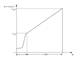
次に、図3を参照すると、図3は、スタイラスに一体化された例示的な圧力センサで検出され得るキャパシタンスの簡略化されたグラフを示している。いくつかの実装では、圧力センサ200からの出力は、スタイラス100のホバリング状態とインク状態とを区別するために印加される。任意で、ホバリングとインクとの間のカットオフは、剛性要素220とエラストマ210との間の所定のレベルのキャパシタンスCH2Tで生じる。1つの例示の実装では、CH2Tは、わずかな力で又は力を伴わずに剛性要素がエラストマ210と係合するときに検出されるキャパシタンスに対応する。
Referring now to FIG. 3, FIG. 3 shows a simplified graph of capacitance that may be detected with an exemplary pressure sensor integrated into the stylus. In some implementations, the output from
スタイラス100のインク状態(又はタッチ状態)の間、剛性要素220は、エラストマ210と係合することができ、容量結合は、力の増加に伴うエラストマ210の漸進的変形による、剛性要素220とエラストマ210との間の表面接触面積の変化によって支配され得る。この曲線の勾配は、典型的に、エラストマ210の硬さと剛性要素220の形状によって支配され得る。
During the inking state (or touch state) of
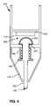
次に、図4を参照すると、図4は、スタイラスと一体化された例示的な圧力センサの代替構成を示す簡略化された概略図を示している。いくつかの実装では、剛性要素220は、書込みチップ153の一部として一体化される。剛性要素220は、端部151に対して遠位の書込みチップ153の端部で形成される。書込みチップ153(剛性要素220を含む)は、金属から機械加工されてもよく、あるいは導電性プラスチックで成形されてもよい。書込みチップ153は、弾性要素160を支持するためのフランジ156を更に含んでもよい。
Referring now to FIG. 4, FIG. 4 shows a simplified schematic diagram showing an alternative configuration of an exemplary pressure sensor integrated with a stylus. In some implementations,
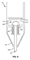
次に、図5を参照すると、図5は、スタイラスと一体化された例示的な圧力センサのための更に別の構成を示す簡略化された概略図を示している。圧力センサ200は、書込みチップ150がニュートラルな状態の間、例えば書込みチップ150の端部151に力が加えられていないとき、剛性要素220がエラストマ210と係合するように組み立てられる。この例示の構成では、(図2Bに示されるような)エアギャップ157は除去される。任意で、エアギャップ157がない構成では、弾性要素160の代わりに(例えば弾性要素160を除去することによって)、弾性要素210の弾性特性を使用することができる。
Referring now to FIG. 5, FIG. 5 shows a simplified schematic diagram showing yet another configuration for an exemplary pressure sensor integrated with a stylus.
次に、図6を参照すると、図6は、スタイラスと一体化された例示的な圧力センサのための代替の誘電体層の簡略化された概略図を示している。剛性要素220とエラストマ210との間の誘電体層215が、剛性要素220の代わりにエラストマ210上に一体化される。例えばエラストマ210は、シリコン又はプラズマのような他の非導電性材料の層でコーティングされてよい。層215は、10nm規模~10μm規模の間、例えば20μm未満の間の範囲の厚さの薄い層であってよい。任意で、層215は、異なる厚さを区別するために色コード化されてもよい。任意で、接触中の剛性要素220との接着を低減するために、層215にテクスチャを加えてもよい。
Referring now to FIG. 6, FIG. 6 shows a simplified schematic diagram of an alternative dielectric layer for an exemplary pressure sensor integrated with a stylus. A
次に、図7を参照すると、図7は、感圧スタイラスを用いて操作される例示のコンピューティングデバイスの簡略化されたブロック図を示している。いくつかの実装によれば、コンピューティングデバイス10は、デジタイザセンサ50に一体化されるディスプレイ画面45を含む。デジタイザセンサ50は、信号を送信する感圧スタイラス100による入力と、1つ以上の指先46又は他の導電性物体による入力との双方を検出するように動作する導電性ストリップ51から形成される、グリッドベースの容量センサとすることができる。デジタイザセンサ50は、デジタイザ回路25によって動作され、ホスト22と通信することができる。
Referring now to FIG. 7, FIG. 7 depicts a simplified block diagram of an exemplary computing device operated using a pressure sensitive stylus. According to some implementations,
スタイラス100のチップに加えられる圧力を、スタイラス100に含まれる圧力センサ200によって感知することができる。いくつかの実施例では、センサ200の出力は、スタイラス100によって送信され、1つ以上の導電線51によってピックアップされる。任意で、センサ200からの出力は、スタイラス100によって送信される位置信号に符号化される。任意で、センサ200によって検出されるインク又はホバリング動作状態を示す情報は、スタイラス100によって送信される位置信号に符号化される。任意で、センサ200からの出力は、デジタイザ回路25によって送信されるクエリ信号に応答して送信される。
Pressure applied to the tip of
デジタイザ回路25からの出力はホスト22に報告される。デジタイザ回路25によって提供される出力は、スタイラス100の座標、スタイラス100のチップの圧力状態やレベル及び/又はデジタイザセンサ50と相互作用する1つ以上の指先46の座標を含む。任意で、デジタイザ回路25はスタイラス100のホバリング又はインク状態を報告する。任意で、デジタイザ回路25は、スタイラスチップに加えられる圧力を報告する。任意で、デジタイザ回路25の機能の一部及び/又は全部が、ホスト22と一体化されるか、かつ/又はホスト22に含まれる。
The output from
いくつかの実装によれば、装置は、ハウジングと;チップであって、該チップに加えられる接触力に基づいてハウジングに対して動くように構成されるチップと;チップの動きに基づいて、チップに加えられる力を検出するように構成される圧力センサであって、該センサは、チップに一体化されるか固定される第1要素であって、導電性の剛性材料から形成される第1要素と、ハウジングに対して静止し、第1要素に対向するように配置される第2要素であって、導電性であり、かつ弾性特性を有する第2要素とを含み、第1要素又は第2要素の一方が、非導電層でコーティングされ、第1要素が、チップに加えられた力に基づいて第2要素の方へ動き、力に基づいて第2要素を変形するように構成される、圧力センサと;第1要素と第2要素との間のキャパシタンスを検出するように構成された回路と;を含む。 According to some implementations, the device includes a housing; a chip configured to move relative to the housing based on a contact force applied to the chip; A pressure sensor configured to detect a force applied to a first element integrated or fixed to the chip, the first element being made of an electrically conductive rigid material. and a second element stationary with respect to the housing and arranged opposite the first element, the second element being electrically conductive and having elastic properties; One of the two elements is coated with a non-conductive layer, the first element configured to move toward the second element based on force applied to the tip and deform the second element based on the force. , a pressure sensor; and circuitry configured to detect capacitance between the first element and the second element.
任意で、第1要素はドーム形状又は円錐形である。 Optionally, the first element is dome-shaped or conical.
任意で、第2要素はエラストマである。 Optionally, the second element is elastomer.
任意で、第2要素は平坦な形状を有する。 Optionally, the second element has a flat shape.
任意で、非導電層は、10nm~20μmの間の厚さである。 Optionally, the non-conducting layer is between 10 nm and 20 μm thick.
任意で、非導電層は、第1要素と第2要素との間の接着を低減するよう構成されるテクスチャを含む。 Optionally, the non-conductive layer includes a texture configured to reduce adhesion between the first element and the second element.
任意で、第1要素は、金属から形成され、非導電層は、金属上に形成される陽極酸化層である。 Optionally, the first element is formed of metal and the non-conductive layer is an anodized layer formed on the metal.
任意で、非導電層は、第2要素上に塗布されたシリコン層である。 Optionally, the non-conductive layer is a silicon layer applied over the second element.
任意で、装置は、ハウジング及びチップに機械的に結合される弾性要素を備え、該弾性要素は、チップに予荷重を与えるように構成される。 Optionally, the device comprises a resilient element mechanically coupled to the housing and the tip, the resilient element configured to preload the tip.
いくつかの実装によれば、スタイラスは、ハウジングと;書込みチップであって、該書込みチップに加えられる接触力に基づいてハウジングに対して動くように構成される書込みチップと;書込みチップの動きに基づいて、書込みチップに加えられる力を検出するように構成される圧力センサであって、該センサは、書込みチップと一緒に動くように構成される第1要素であって、導電性の剛性材料から形成される第1要素と、ハウジングに対して静止し、第1要素に対向するように配置される第2要素であって、導電性エラストマである第2要素とを含み、第1要素の1つが、非導電層でコーティングされ、第1要素が、チップに加えられた力に基づいて第2要素の方へ動き、力に基づいて第2要素を変形するように構成される、圧力センサと;第1要素と第2要素との間のキャパシタンスを検出するように構成された回路と;を含む。 According to some implementations, the stylus includes a housing; a writing tip configured to move relative to the housing based on a contact force applied to the writing tip; A pressure sensor configured to detect a force applied to the writing tip, the sensor being a first element configured to move with the writing tip and comprising a conductive rigid material. and a second element stationary relative to the housing and positioned opposite the first element, the second element being an electrically conductive elastomer, the first element comprising: A pressure sensor, one of which is coated with a non-conductive layer and configured to move a first element toward a second element based on a force applied to the tip and deform the second element based on the force. and; circuitry configured to detect capacitance between the first element and the second element.
任意で、第1要素はドーム形状又は円錐形である。 Optionally, the first element is dome-shaped or conical.
任意で、書込みチップは、ハウジングの外に延びるよう構成される第1端部と、ハウジング内に維持される第2端部とを含む細長い要素であり、第2端部は第1要素を含む。 Optionally, the writing tip is an elongated element including a first end configured to extend out of the housing and a second end retained within the housing, the second end including the first element. .
任意で、書込みチップは、金属から機械加工される。 Optionally, the writing tip is machined from metal.
任意で、書込みチップは、導電性プラスチックで成形される。 Optionally, the writing tip is molded of conductive plastic.
任意で、スタイラスは、チップホルダを備え、書込みチップは、ハウジングの外に延びるよう構成される第1端部と、ハウジング内に維持される第2端部とを含む細長い要素であり、チップホルダは、書込みチップの第2端部に接続され、第1要素を含む。 Optionally, the stylus comprises a tip holder, the writing tip being an elongated element including a first end configured to extend out of the housing and a second end retained within the housing, the tip holder is connected to the second end of the writing tip and includes a first element.
任意で、第2要素は平坦な形状を有する。 Optionally, the second element has a flat shape.
任意で、非導電層は、10nm~20μmの間の厚さである。 Optionally, the non-conducting layer is between 10 nm and 20 μm thick.
任意で、非導電層は、規定されたテクスチャでパターニングされる。 Optionally, the non-conductive layer is patterned with a defined texture.
任意で、第1要素は、金属から形成され、非導電層は、金属上にコーティングされた着色層(colored layer)ある。 Optionally, the first element is formed of metal and the non-conductive layer is a colored layer coated onto the metal.
任意で、スタイラスは、ハウジング及び書込みチップに機械的に結合されるバネを含み、該バネは、書込みチップに予荷重を与えるように構成される。 Optionally, the stylus includes a spring mechanically coupled to the housing and the writing tip, the spring configured to preload the writing tip.
明確性のために別個の実施形態の文脈で説明される、本明細書に記載した実施例の特定の特徴は、単一の実施形態において組み合わせて提供されてもよい。反対に、簡潔性のために単一の実施形態の文脈で説明される、本明細書に記載した実施例の様々な特徴は、別個に又は任意の適切な副次的組合せで、あるいは本開示の説明された任意の他の実施形態において適切であるように提供されてもよい。様々な実施形態の文脈で説明される特定の特徴は、実施形態がそれらの要素なしで動作不能でない限り、それらの実施形態の本質的な特徴とはみなされない。
Certain features of the examples described herein that are, for clarity, described in the context of separate embodiments may also be provided in combination in a single embodiment. Conversely, various features of the embodiments described herein, which are, for brevity's sake, described in the context of a single embodiment, may be combined separately or in any suitable subcombination or otherwise disclosed herein. may be provided as appropriate in any other described embodiment of. Certain features described in the context of various embodiments are not considered essential features of those embodiments unless the embodiments are inoperable without those elements.
Claims (20)
チップであって、該チップに加えられる接触力に基づいて前記ハウジングに対して動くように構成されるチップと;
前記チップの動きに基づいて前記チップに加えられる力を検出するように構成される圧力センサであって、該センサは、
前記チップに一体化されるか固定される第1要素であって、導電性の剛性材料から形成される第1要素と、
前記ハウジングに対して静止し、前記第1要素に対向するように配置される第2要素であって、導電性であり、かつ弾性特性を有する第2要素と、
を含み、前記第1要素又は前記第2要素の一方が、10nm~20μmの間の厚さの非導電層でコーティングされ、前記第1要素が、前記チップに加えられた力に基づいて前記第2要素の方へ動き、前記力に基づいて前記第2要素を変形するように構成される、前記圧力センサと;
前記第1要素と前記第2要素との間のキャパシタンスを検出するように構成された回路と;
を含む、装置。 a housing;
a tip configured to move relative to the housing based on a contact force applied to the tip;
A pressure sensor configured to detect a force applied to the tip based on movement of the tip, the sensor comprising:
a first element integral with or fixed to the chip, the first element being formed of a conductive rigid material;
a second element stationary with respect to the housing and arranged opposite the first element, the second element being electrically conductive and having elastic properties;
wherein one of said first element or said second element is coated with a non-conductive layer having a thickness between 10 nm and 20 μm, and said first element reacts with said second element based on a force applied to said tip. said pressure sensor configured to move towards two elements and deform said second element based on said force;
circuitry configured to detect capacitance between the first element and the second element;
apparatus, including
請求項1に記載の装置。 the first element is dome-shaped or conical;
A device according to claim 1 .
請求項1又は2に記載の装置。 wherein said second element is an elastomer;
3. Apparatus according to claim 1 or 2.
請求項1乃至3のいずれか一項に記載の装置。 the second element has a flat shape;
4. Apparatus according to any one of claims 1-3.
請求項1乃至4のいずれか一項に記載の装置。 the non-conductive layer includes a texture configured to reduce adhesion between the first element and the second element;
5. Apparatus according to any one of claims 1-4 .
請求項1乃至5のいずれか一項に記載の装置。 wherein said first element is formed of metal and said non-conductive layer is an anodized layer formed on said metal;
6. Apparatus according to any one of claims 1-5 .
請求項1乃至5のいずれか一項に記載の装置。 the non-conductive layer is a silicon layer applied on the second element;
6. Apparatus according to any one of claims 1-5 .
請求項1乃至7のいずれか一項に記載の装置。 a resilient element mechanically coupled to the housing and the tip, the resilient element configured to preload the tip;
8. Apparatus according to any one of claims 1-7 .
書込みチップであって、該書込みチップに加えられる接触力に基づいて前記ハウジングに対して動くように構成される書込みチップと; a writing tip configured to move relative to the housing based on a contact force applied to the writing tip;
前記書込みチップの動きに基づいて前記書込みチップに加えられる力を検出するように構成される圧力センサであって、該センサは、 A pressure sensor configured to detect a force applied to the writing tip based on movement of the writing tip, the sensor comprising:
前記書込みチップに一体化されるか固定される第1要素であって、導電性の剛性材料から形成される第1要素と、 a first element integral with or fixed to the writing tip, the first element being formed of a conductive rigid material;
前記ハウジングに対して静止し、前記第1要素に対向するように配置される第2要素であって、導電性であり、かつ弾性特性を有する第2要素と、 a second element stationary with respect to the housing and arranged opposite the first element, the second element being electrically conductive and having elastic properties;
を含み、前記第1要素又は前記第2要素の一方が、10nm~20μmの間の厚さの非導電層でコーティングされ、前記第1要素が、前記書込みチップに加えられた力に基づいて前記第2要素の方へ動き、前記力に基づいて前記第2要素を変形するように構成される、前記圧力センサと; wherein one of the first element or the second element is coated with a non-conductive layer having a thickness between 10 nm and 20 μm, the first element being actuated based on a force applied to the writing tip said pressure sensor configured to move towards a second element and deform said second element based on said force;
前記第1要素と前記第2要素との間のキャパシタンスを検出するように構成された回路と; circuitry configured to detect capacitance between the first element and the second element;
を含む、 including,
スタイラス。 stylus.
請求項9に記載のスタイラス。 A stylus according to claim 9 .
請求項9又は10に記載のスタイラス。 The writing tip is an elongated element including a first end configured to extend out of the housing and a second end retained within the housing, the second end being the first element. including,
A stylus according to claim 9 or 10.
請求項11に記載のスタイラス。 the writing tip is machined from metal;
12. The stylus of claim 11.
請求項11に記載のスタイラス。 the writing tip is molded of conductive plastic;
12. The stylus of claim 11.
請求項9に記載のスタイラス。 a tip holder, the writing tip being an elongated element including a first end configured to extend out of the housing and a second end retained within the housing, the tip holder comprising: connected to the second end of the writing tip and including the first element;
A stylus according to claim 9 .
請求項9乃至14のいずれか一項に記載のスタイラス。 the second element has a flat shape;
15. A stylus according to any one of claims 9-14 .
請求項9乃至15のいずれか一項に記載のスタイラス。 16. A stylus according to any one of claims 9-15.
請求項9乃至16のいずれか一項に記載のスタイラス。 17. A stylus according to any one of claims 9-16.
スタイラスであって: With a stylus:
ハウジングと; a housing;
書込みチップであって、該書込みチップに加えられる接触力に基づいて前記ハウジングに対して動くように構成される書込みチップと; a writing tip configured to move relative to the housing based on a contact force applied to the writing tip;
前記書込みチップの動きに基づいて前記書込みチップに加えられる力を検出するように構成される圧力センサであって、該センサは、 A pressure sensor configured to detect a force applied to the writing tip based on movement of the writing tip, the sensor comprising:
前記書込みチップと一緒に動くように構成される第1要素であって、導電性の剛性材料から形成される第1要素と、 a first element configured to move with the writing tip, the first element formed from an electrically conductive rigid material;
前記ハウジングに対して静止し、前記第1要素に対向するように配置される第2要素であって、導電性エラストマである第2要素と、 a second element stationary relative to the housing and positioned opposite the first element, the second element being an electrically conductive elastomer;
を含み、前記第1要素又は前記第2要素の一方が、10nm~20μmの間の厚さの非導電層でコーティングされ、前記第1要素が、前記書込みチップに加えられた力に基づいて前記第2要素の方へ動き、前記力に基づいて前記第2要素を変形するように構成される、前記圧力センサと; wherein one of the first element or the second element is coated with a non-conductive layer having a thickness between 10 nm and 20 μm, the first element being actuated based on a force applied to the writing tip said pressure sensor configured to move towards a second element and deform said second element based on said force;
前記第1要素と前記第2要素との間のキャパシタンスを検出するように構成された回路と; circuitry configured to detect capacitance between the first element and the second element;
を含む、スタイラス;を含む、 including a stylus; including
システム。 system.
請求項18に記載のシステム。 19. System according to claim 18.
請求項18に記載のシステム。 19. System according to claim 18.
Priority Applications (1)
| Application Number | Priority Date | Filing Date | Title |
|---|---|---|---|
| JP2022129887A JP7443434B2 (en) | 2017-01-30 | 2022-08-17 | pressure sensitive stylus |
Applications Claiming Priority (3)
| Application Number | Priority Date | Filing Date | Title |
|---|---|---|---|
| US15/418,823 US10318022B2 (en) | 2017-01-30 | 2017-01-30 | Pressure sensitive stylus |
| US15/418,823 | 2017-01-30 | ||
| PCT/US2018/014754 WO2018140364A1 (en) | 2017-01-30 | 2018-01-23 | Pressure sensitive stylus |
Related Child Applications (1)
| Application Number | Title | Priority Date | Filing Date |
|---|---|---|---|
| JP2022129887A Division JP7443434B2 (en) | 2017-01-30 | 2022-08-17 | pressure sensitive stylus |
Publications (2)
| Publication Number | Publication Date |
|---|---|
| JP2020505706A JP2020505706A (en) | 2020-02-20 |
| JP7127040B2 true JP7127040B2 (en) | 2022-08-29 |
Family
ID=61193039
Family Applications (2)
| Application Number | Title | Priority Date | Filing Date |
|---|---|---|---|
| JP2019541136A Active JP7127040B2 (en) | 2017-01-30 | 2018-01-23 | pressure sensitive stylus |
| JP2022129887A Active JP7443434B2 (en) | 2017-01-30 | 2022-08-17 | pressure sensitive stylus |
Family Applications After (1)
| Application Number | Title | Priority Date | Filing Date |
|---|---|---|---|
| JP2022129887A Active JP7443434B2 (en) | 2017-01-30 | 2022-08-17 | pressure sensitive stylus |
Country Status (18)
| Country | Link |
|---|---|
| US (3) | US10318022B2 (en) |
| EP (1) | EP3574390B1 (en) |
| JP (2) | JP7127040B2 (en) |
| KR (1) | KR102407672B1 (en) |
| CN (2) | CN110235090B (en) |
| AU (1) | AU2018213046B2 (en) |
| BR (1) | BR112019012067A2 (en) |
| CA (1) | CA3049257A1 (en) |
| CL (1) | CL2019002043A1 (en) |
| CO (1) | CO2019007707A2 (en) |
| IL (1) | IL268032B (en) |
| MX (1) | MX2019008800A (en) |
| MY (1) | MY205836A (en) |
| NZ (1) | NZ754550A (en) |
| PH (1) | PH12019550124A1 (en) |
| RU (1) | RU2019126647A (en) |
| SG (1) | SG11201906573XA (en) |
| WO (1) | WO2018140364A1 (en) |
Families Citing this family (12)
| Publication number | Priority date | Publication date | Assignee | Title |
|---|---|---|---|---|
| TWI706297B (en) * | 2019-02-27 | 2020-10-01 | 群光電子股份有限公司 | Touching stylus |
| US11043945B2 (en) * | 2019-03-22 | 2021-06-22 | Yingchao WU | Capacitance-variable pressure sensor |
| CN110058704B (en) * | 2019-04-09 | 2025-07-04 | 惠州市创锋科技有限公司 | An electronic touch pen with pressure-sensitive structure and overload protection function |
| EP3789855A1 (en) | 2019-09-05 | 2021-03-10 | Microsoft Technology Licensing, LLC | Stylus nib design and accuracy improvement |
| CN111351604B (en) * | 2020-04-15 | 2022-07-26 | 深圳市欣智旺电子有限公司 | Electronic pen pressure sensor protection device and electronic pen |
| CN111538425B (en) * | 2020-04-21 | 2025-10-17 | 深圳市欣威智能有限公司 | Nib pressure-sensitive structure and electronic pen |
| EP4339747A4 (en) * | 2021-05-13 | 2024-08-07 | Wacom Co., Ltd. | ELECTRONIC PEN AND CORE BODY FOR ELECTRONIC PEN |
| TWI788878B (en) * | 2021-06-11 | 2023-01-01 | 立邁科技股份有限公司 | Active stylus |
| CN113415098B (en) * | 2021-07-24 | 2025-07-25 | 温州市蓝图文具有限公司 | Electronic pen |
| KR102410654B1 (en) | 2022-03-04 | 2022-06-22 | 유성목 | Input Device For Virtual Reality And Augmented Reality |
| US12050740B2 (en) | 2022-11-29 | 2024-07-30 | Sigmasense, Llc. | Passive device with compressible pressure assembly for Z-direction capacitance detection |
| WO2025116829A1 (en) * | 2023-11-30 | 2025-06-05 | Nanyang Technological University | Quant-haptical device for quantitative measurement |
Citations (2)
| Publication number | Priority date | Publication date | Assignee | Title |
|---|---|---|---|---|
| JP2010117943A (en) | 2008-11-13 | 2010-05-27 | Wacom Co Ltd | Position indicator, variable capacitor and input device |
| US20150317001A1 (en) | 2014-05-04 | 2015-11-05 | Microsoft Technology Licensing, Llc | Pressure sensor for a stylus |
Family Cites Families (115)
| Publication number | Priority date | Publication date | Assignee | Title |
|---|---|---|---|---|
| US4111052A (en) | 1977-08-29 | 1978-09-05 | Burroughs Corporation | Pressure-sensitive writing stylus |
| US4451698A (en) | 1982-11-12 | 1984-05-29 | Display Interface Corporation | Coordinate digitizing device |
| US4672154A (en) | 1985-04-03 | 1987-06-09 | Kurta Corporation | Low power, high resolution digitizing system with cordless pen/mouse |
| EP0209467A3 (en) | 1985-07-18 | 1988-09-28 | Schlumberger Systems Inc. | Improved stylus for use with digitizer tablets |
| US5251123A (en) | 1987-10-19 | 1993-10-05 | I C Operating, Inc. | High resolution system for sensing spatial coordinates |
| US5004872A (en) | 1989-11-14 | 1991-04-02 | Summagraphics Corporation | Digitizer tablet with pressure stylus |
| JP3150685B2 (en) * | 1990-08-06 | 2001-03-26 | 株式会社ワコム | Variable capacitance capacitor |
| US5138118A (en) | 1991-05-06 | 1992-08-11 | International Business Machines Corporation | Pulsed pen for use with a digitizer tablet |
| US5225637A (en) | 1991-10-01 | 1993-07-06 | Kurta Corporation | Position resolving system |
| JP2839804B2 (en) | 1992-10-08 | 1998-12-16 | シャープ株式会社 | Coordinate detection device |
| US5414227A (en) | 1993-04-29 | 1995-05-09 | International Business Machines Corporation | Stylus tilt detection apparatus for communication with a remote digitizing display |
| US5528002A (en) | 1993-07-15 | 1996-06-18 | Pentel Kabushiki Kaisha | Noiseproof digitizing apparatus with low power cordless pen |
| US5571997A (en) | 1993-08-02 | 1996-11-05 | Kurta Corporation | Pressure sensitive pointing device for transmitting signals to a tablet |
| JPH09503879A (en) | 1993-10-18 | 1997-04-15 | サマグラフィクス コーポレイション | Pressure sensitive stylus with elastically compressible tip element |
| US6249234B1 (en) | 1994-05-14 | 2001-06-19 | Absolute Sensors Limited | Position detector |
| JPH08227336A (en) | 1995-02-20 | 1996-09-03 | Wacom Co Ltd | Pressure-sensitive mechanism and stylus pen |
| US5793360A (en) | 1995-05-05 | 1998-08-11 | Wacom Co., Ltd. | Digitizer eraser system and method |
| JP2767098B2 (en) | 1995-06-06 | 1998-06-18 | 株式会社ワコム | Position indicating unit and stylus pen |
| JP3327056B2 (en) | 1995-06-27 | 2002-09-24 | 日本電信電話株式会社 | Pen-type input device |
| US5914708A (en) | 1996-04-04 | 1999-06-22 | Cirque Corporation | Computer input stylus method and apparatus |
| US6707451B1 (en) | 1996-09-11 | 2004-03-16 | Pilot Precision Kabushiki Kaisha | Input pen |
| JP3475048B2 (en) | 1997-07-18 | 2003-12-08 | シャープ株式会社 | Handwriting input device |
| US6624832B1 (en) | 1997-10-29 | 2003-09-23 | Ericsson Inc. | Methods, apparatus and computer program products for providing user input to an application using a contact-sensitive surface |
| GB2332056B (en) | 1997-12-04 | 2000-08-09 | Taylor Hobson Ltd | Surface measuring apparatus |
| US6211863B1 (en) | 1998-05-14 | 2001-04-03 | Virtual Ink. Corp. | Method and software for enabling use of transcription system as a mouse |
| US6232962B1 (en) | 1998-05-14 | 2001-05-15 | Virtual Ink Corporation | Detector assembly for use in a transcription system |
| WO2001024157A1 (en) | 1999-09-29 | 2001-04-05 | James Loke Kie Chan | A method and apparatus for detecting depression pressure in a stylus |
| US6808330B1 (en) | 1999-10-25 | 2004-10-26 | Silverbrook Research Pty Ltd | Universal pen with sampler |
| JP4376425B2 (en) | 2000-05-08 | 2009-12-02 | 株式会社ワコム | Variable capacitor and position indicator |
| US7657128B2 (en) | 2000-05-23 | 2010-02-02 | Silverbrook Research Pty Ltd | Optical force sensor |
| US6690156B1 (en) | 2000-07-28 | 2004-02-10 | N-Trig Ltd. | Physical object location apparatus and method and a graphic display device using the same |
| US7102628B2 (en) | 2000-10-06 | 2006-09-05 | International Business Machines Corporation | Data steering flip pen system |
| SI20774A (en) | 2000-11-20 | 2002-06-30 | Janez Stare | 3D sensitive board |
| AU2002226969A1 (en) | 2000-11-22 | 2002-06-03 | Cirque Corporation | Stylus input device utilizing a permanent magnet |
| US7279646B2 (en) | 2001-05-25 | 2007-10-09 | Intel Corporation | Digital signature collection and authentication |
| US6727439B2 (en) | 2002-01-28 | 2004-04-27 | Aiptek International Inc. | Pressure sensitive pen |
| US7120872B2 (en) | 2002-03-25 | 2006-10-10 | Microsoft Corporation | Organizing, editing, and rendering digital ink |
| US6972754B2 (en) | 2002-06-27 | 2005-12-06 | Topaz Systems, Inc. | Touchpad stylus having isolated low-mass contact element |
| EP2388770A1 (en) | 2002-08-29 | 2011-11-23 | N-Trig Ltd. | Digitizer stylus |
| CN101261561A (en) | 2003-02-10 | 2008-09-10 | N-特莱格有限公司 | Touch detection for a digitizer |
| GB0319945D0 (en) | 2003-08-26 | 2003-09-24 | Synaptics Uk Ltd | Inductive sensing system |
| US20050110777A1 (en) | 2003-11-25 | 2005-05-26 | Geaghan Bernard O. | Light-emitting stylus and user input device using same |
| US7210046B2 (en) | 2004-01-23 | 2007-04-24 | Dell Products L.P. | System, method and software for power management in a stylus input enabled information handling system |
| US7202862B1 (en) | 2004-03-03 | 2007-04-10 | Finepoint Innovations, Inc. | Pressure sensor for a digitizer pen |
| US7023536B2 (en) | 2004-03-08 | 2006-04-04 | Electronic Scripting Products, Inc. | Apparatus and method for determining orientation parameters of an elongate object |
| US20060068851A1 (en) | 2004-09-28 | 2006-03-30 | Ashman William C Jr | Accessory device for mobile communication device |
| US7847789B2 (en) | 2004-11-23 | 2010-12-07 | Microsoft Corporation | Reducing accidental touch-sensitive device activation |
| JP2008522183A (en) | 2004-12-01 | 2008-06-26 | エヌ−トリグ リミテッド | Position detection system and apparatus and method for its use and control |
| US8228299B1 (en) | 2005-01-27 | 2012-07-24 | Singleton Technology, Llc | Transaction automation and archival system using electronic contract and disclosure units |
| US7367242B2 (en) | 2005-03-02 | 2008-05-06 | Board Of Trustees Operating Michigan State University | Active sensor for micro force measurement |
| US20060267966A1 (en) | 2005-05-24 | 2006-11-30 | Microsoft Corporation | Hover widgets: using the tracking state to extend capabilities of pen-operated devices |
| US7928967B2 (en) | 2005-08-19 | 2011-04-19 | Silverbrook Research Pty Ltd | Force sensor with angled coupling |
| US20070146351A1 (en) | 2005-12-12 | 2007-06-28 | Yuji Katsurahira | Position input device and computer system |
| US20070176909A1 (en) | 2006-02-02 | 2007-08-02 | Eric Pavlowski | Wireless Mobile Pen Communications Device With Optional Holographic Data Transmission And Interaction Capabilities |
| US8686964B2 (en) | 2006-07-13 | 2014-04-01 | N-Trig Ltd. | User specific recognition of intended user interaction with a digitizer |
| US20080202251A1 (en) | 2007-02-27 | 2008-08-28 | Iee International Electronics & Engineering S.A. | Capacitive pressure sensor |
| JP5109171B2 (en) | 2007-09-18 | 2012-12-26 | 株式会社ワコム | Position indicator, position input device, and computer system |
| WO2009040815A1 (en) | 2007-09-26 | 2009-04-02 | N-Trig Ltd. | Method for identifying changes in signal frequencies emitted by a stylus interacting with a digitizer sensor |
| US8184109B2 (en) | 2007-10-24 | 2012-05-22 | Wacom Co., Ltd. | Coordinate input device, position indicator and variable capacitor |
| EP2204724A4 (en) | 2007-10-26 | 2012-06-13 | Nec Corp | Electronic device, electronic device control method, and storage medium containing electronic device control program |
| US20090122029A1 (en) | 2007-11-13 | 2009-05-14 | Newvit Co. Ltd. | Stylus pen |
| US20100214252A1 (en) | 2007-12-14 | 2010-08-26 | Mao-Sung Wu | Touch panel component for capacitive panel |
| US8125469B2 (en) | 2008-04-18 | 2012-02-28 | Synaptics, Inc. | Passive stylus for capacitive sensors |
| US8212795B2 (en) | 2008-05-21 | 2012-07-03 | Hypercom Corporation | Payment terminal stylus with touch screen contact detection |
| US20100006350A1 (en) | 2008-07-11 | 2010-01-14 | Elias John G | Stylus Adapted For Low Resolution Touch Sensor Panels |
| US8536471B2 (en) | 2008-08-25 | 2013-09-17 | N-Trig Ltd. | Pressure sensitive stylus for a digitizer |
| TWM350750U (en) | 2008-10-03 | 2009-02-11 | Inventec Appliances Corp | Electric pen |
| GB2466566B (en) | 2008-12-22 | 2010-12-22 | N trig ltd | Digitizer, stylus and method of synchronization therewith |
| US20100194693A1 (en) | 2009-01-30 | 2010-08-05 | Sony Ericsson Mobile Communications Ab | Electronic apparatus, method and computer program with adaptable user interface environment |
| JP5430339B2 (en) | 2009-10-19 | 2014-02-26 | 株式会社ワコム | Position detecting device and position indicator |
| JP5345050B2 (en) | 2009-12-25 | 2013-11-20 | 株式会社ワコム | Indicator, position detection device and position detection method |
| US8917262B2 (en) | 2010-01-08 | 2014-12-23 | Integrated Digital Technologies, Inc. | Stylus and touch input system |
| JP5442479B2 (en) | 2010-02-05 | 2014-03-12 | 株式会社ワコム | Indicator, position detection device and position detection method |
| JP5483430B2 (en) | 2010-03-31 | 2014-05-07 | 株式会社ワコム | Variable capacitor and position indicator |
| TW201145093A (en) | 2010-06-10 | 2011-12-16 | Hon Hai Prec Ind Co Ltd | Handheld input device |
| US9239637B2 (en) | 2010-08-30 | 2016-01-19 | Perceptive Pixel, Inc. | Systems for an electrostatic stylus within a capacitive touch sensor |
| JP4683505B1 (en) | 2010-12-14 | 2011-05-18 | 株式会社ワコム | Position indicator |
| US8947404B2 (en) | 2011-03-09 | 2015-02-03 | Atmel Corporation | Stylus |
| WO2012123951A2 (en) | 2011-03-17 | 2012-09-20 | N-Trig Ltd. | Interacting tips for a digitizer stylus |
| JP5375863B2 (en) | 2011-03-29 | 2013-12-25 | カシオ計算機株式会社 | Input device, rotation angle calculation method, and writing pressure calculation method |
| US20120280947A1 (en) | 2011-05-06 | 2012-11-08 | 3M Innovative Properties Company | Stylus with pressure sensitive membrane |
| US20120327040A1 (en) | 2011-06-22 | 2012-12-27 | Simon David I | Identifiable stylus |
| US8878823B1 (en) | 2011-07-27 | 2014-11-04 | Cypress Semiconductor Corporation | Dynamic shield electrode of a stylus |
| US9195351B1 (en) * | 2011-09-28 | 2015-11-24 | Amazon Technologies, Inc. | Capacitive stylus |
| US9116558B2 (en) | 2011-10-28 | 2015-08-25 | Atmel Corporation | Executing gestures with active stylus |
| US9063591B2 (en) | 2011-11-30 | 2015-06-23 | Google Technology Holdings LLC | Active styluses for interacting with a mobile device |
| KR20130061958A (en) | 2011-12-02 | 2013-06-12 | 한국전자통신연구원 | Device for calibrating writing pressure in electronic pen |
| EP2650758B1 (en) | 2012-04-11 | 2017-08-30 | BlackBerry Limited | Force-sensing stylus pointing device |
| WO2013160887A1 (en) | 2012-04-23 | 2013-10-31 | N-Trig Ltd. | Pressure sensitive stylus for a digitizer |
| WO2013179291A1 (en) | 2012-05-31 | 2013-12-05 | N-Trig Ltd. | Writing tip for a stylus |
| JP5939633B2 (en) * | 2012-07-05 | 2016-06-22 | 株式会社ワコム | Capacitance variable capacitor |
| US9372553B2 (en) | 2012-07-10 | 2016-06-21 | Microsoft Technology Licensing, Llc | Directional force sensing for styli |
| WO2014043239A2 (en) | 2012-09-11 | 2014-03-20 | The Cleveland Clinic Foundation | Evaluation of movement disorders |
| JP6038572B2 (en) * | 2012-09-26 | 2016-12-07 | 株式会社ワコム | Position indicator and electronic ink cartridge |
| KR101429925B1 (en) | 2012-11-13 | 2014-08-13 | 엘지디스플레이 주식회사 | Input System |
| US9158393B2 (en) | 2012-12-18 | 2015-10-13 | Logitech Europe S.A. | Active stylus for touch sensing applications |
| CN105027025A (en) | 2013-01-27 | 2015-11-04 | 微软科技许可有限公司 | Digitizer system with improved response time to wake up signal |
| US20140218343A1 (en) | 2013-02-01 | 2014-08-07 | Barnesandnoble.Com Llc | Stylus sensitive device with hover over stylus gesture functionality |
| JP6137610B2 (en) | 2013-04-10 | 2017-05-31 | 株式会社ワコム | Position indicator |
| CN105474138A (en) * | 2013-05-20 | 2016-04-06 | 微软技术许可有限责任公司 | Stylus piezoresistive sensor |
| EP2818981A1 (en) | 2013-06-28 | 2014-12-31 | BlackBerry Limited | Method and apparatus pertaining to switching stylus transmissions between stylus-modality signals and non-stylus-modality signals |
| US9785263B2 (en) * | 2013-08-22 | 2017-10-10 | Microchip Technology Incorporated | Touch screen stylus with force and/or angle sensing functionality |
| JP2015043159A (en) | 2013-08-26 | 2015-03-05 | シャープ株式会社 | Touch panel device and display device |
| US9513721B2 (en) | 2013-09-12 | 2016-12-06 | Microsoft Technology Licensing, Llc | Pressure sensitive stylus for a digitizer |
| US10191568B2 (en) | 2013-10-08 | 2019-01-29 | Microsoft Technology Licensing, Llc | Deformable input device |
| TWI638291B (en) * | 2013-11-08 | 2018-10-11 | 禾瑞亞科技股份有限公司 | Method, touch sensitive processing apparatus and system for detecting transmitter |
| CN105829997B (en) * | 2013-12-25 | 2019-05-17 | 株式会社和冠 | Position instruction module and stylus |
| KR20150094797A (en) * | 2014-02-07 | 2015-08-20 | (주) 태양기전 | Portable Electric Input Device |
| US9389708B2 (en) | 2014-05-08 | 2016-07-12 | Atmel Corporation | Active stylus with force sensor |
| TWI556140B (en) | 2014-10-17 | 2016-11-01 | 致伸科技股份有限公司 | Stylus |
| US9874951B2 (en) | 2014-11-03 | 2018-01-23 | Microsoft Technology Licensing, Llc | Stylus for operating a digitizer system |
| US20160162045A1 (en) | 2014-12-09 | 2016-06-09 | Cirque Corporation | Paint brush capacitive stylus tip |
| TWI514206B (en) | 2015-03-17 | 2015-12-21 | Capacitive pointer | |
| US9740312B2 (en) | 2015-09-09 | 2017-08-22 | Microsoft Technology Licensing, Llc | Pressure sensitive stylus |
| CN205594600U (en) * | 2016-04-22 | 2016-09-21 | 立迈科技股份有限公司 | Active pressure sensitive capacitive stylus |
-
2017
- 2017-01-30 US US15/418,823 patent/US10318022B2/en active Active
-
2018
- 2018-01-23 KR KR1020197025597A patent/KR102407672B1/en active Active
- 2018-01-23 EP EP18704658.6A patent/EP3574390B1/en active Active
- 2018-01-23 CA CA3049257A patent/CA3049257A1/en active Pending
- 2018-01-23 SG SG11201906573XA patent/SG11201906573XA/en unknown
- 2018-01-23 CN CN201880009186.3A patent/CN110235090B/en active Active
- 2018-01-23 BR BR112019012067-0A patent/BR112019012067A2/en not_active Application Discontinuation
- 2018-01-23 JP JP2019541136A patent/JP7127040B2/en active Active
- 2018-01-23 MX MX2019008800A patent/MX2019008800A/en unknown
- 2018-01-23 NZ NZ754550A patent/NZ754550A/en not_active IP Right Cessation
- 2018-01-23 MY MYPI2019004030A patent/MY205836A/en unknown
- 2018-01-23 WO PCT/US2018/014754 patent/WO2018140364A1/en not_active Ceased
- 2018-01-23 CN CN202211480289.2A patent/CN115756186A/en active Pending
- 2018-01-23 RU RU2019126647A patent/RU2019126647A/en not_active Application Discontinuation
- 2018-01-23 AU AU2018213046A patent/AU2018213046B2/en not_active Ceased
-
2019
- 2019-05-07 US US16/405,976 patent/US11169624B2/en active Active
- 2019-07-02 PH PH12019550124A patent/PH12019550124A1/en unknown
- 2019-07-14 IL IL268032A patent/IL268032B/en unknown
- 2019-07-22 CO CONC2019/0007707A patent/CO2019007707A2/en unknown
- 2019-07-22 CL CL2019002043A patent/CL2019002043A1/en unknown
-
2021
- 2021-10-15 US US17/503,248 patent/US20220075462A1/en not_active Abandoned
-
2022
- 2022-08-17 JP JP2022129887A patent/JP7443434B2/en active Active
Patent Citations (2)
| Publication number | Priority date | Publication date | Assignee | Title |
|---|---|---|---|---|
| JP2010117943A (en) | 2008-11-13 | 2010-05-27 | Wacom Co Ltd | Position indicator, variable capacitor and input device |
| US20150317001A1 (en) | 2014-05-04 | 2015-11-05 | Microsoft Technology Licensing, Llc | Pressure sensor for a stylus |
Also Published As
| Publication number | Publication date |
|---|---|
| SG11201906573XA (en) | 2019-08-27 |
| CN115756186A (en) | 2023-03-07 |
| EP3574390A1 (en) | 2019-12-04 |
| PH12019550124A1 (en) | 2020-06-01 |
| US20180217684A1 (en) | 2018-08-02 |
| AU2018213046B2 (en) | 2021-11-11 |
| US20190265810A1 (en) | 2019-08-29 |
| JP2022167940A (en) | 2022-11-04 |
| IL268032A (en) | 2019-09-26 |
| CA3049257A1 (en) | 2018-08-02 |
| CN110235090A (en) | 2019-09-13 |
| IL268032B (en) | 2022-01-01 |
| CN110235090B (en) | 2022-12-06 |
| JP7443434B2 (en) | 2024-03-05 |
| US20220075462A1 (en) | 2022-03-10 |
| WO2018140364A1 (en) | 2018-08-02 |
| US11169624B2 (en) | 2021-11-09 |
| KR20190110610A (en) | 2019-09-30 |
| BR112019012067A2 (en) | 2020-01-07 |
| CO2019007707A2 (en) | 2019-10-09 |
| US10318022B2 (en) | 2019-06-11 |
| RU2019126647A (en) | 2021-03-01 |
| EP3574390B1 (en) | 2021-09-29 |
| JP2020505706A (en) | 2020-02-20 |
| CL2019002043A1 (en) | 2019-12-13 |
| AU2018213046A1 (en) | 2019-07-04 |
| MY205836A (en) | 2024-11-15 |
| MX2019008800A (en) | 2019-09-11 |
| NZ754550A (en) | 2023-05-26 |
| KR102407672B1 (en) | 2022-06-10 |
Similar Documents
| Publication | Publication Date | Title |
|---|---|---|
| JP7443434B2 (en) | pressure sensitive stylus | |
| CN106575167B (en) | The pressure-sensitive stylus of digitizer | |
| US9389708B2 (en) | Active stylus with force sensor | |
| EP3347797B1 (en) | Pressure sensitive stylus | |
| US20150317001A1 (en) | Pressure sensor for a stylus | |
| US8400402B2 (en) | Electronic device housing with integrated user input capability | |
| CN105474138A (en) | Stylus piezoresistive sensor | |
| CN208766625U (en) | Capacitance sensor and for detecting the degree of approach, touch and the system of pressure | |
| US20150138165A1 (en) | Replaceable Tip for Active Stylus | |
| TW201409291A (en) | Stylus and capacitive pressure sensing element employed therein | |
| JP2015152429A (en) | Pressure sensor, and stylus pen | |
| HK40011799B (en) | Pressure sensitive stylus | |
| KR102550768B1 (en) | Integrated system comprising capacity sensor and vibration actuator based on magnetorheological elastomer | |
| HK40011799A (en) | Pressure sensitive stylus | |
| EP3177984B1 (en) | Pressure sensitive stylus for a digitizer | |
| TWI522872B (en) | Contact detection method for touch pen and capacitive touch panel for capacitive touch panel | |
| CN101788858A (en) | Contact detection method of capacitive touch panel and stylus thereof | |
| KR101673135B1 (en) | Digitizer system |
Legal Events
| Date | Code | Title | Description |
|---|---|---|---|
| A621 | Written request for application examination |
Free format text: JAPANESE INTERMEDIATE CODE: A621 Effective date: 20201221 |
|
| A977 | Report on retrieval |
Free format text: JAPANESE INTERMEDIATE CODE: A971007 Effective date: 20211130 |
|
| A131 | Notification of reasons for refusal |
Free format text: JAPANESE INTERMEDIATE CODE: A131 Effective date: 20211207 |
|
| A521 | Request for written amendment filed |
Free format text: JAPANESE INTERMEDIATE CODE: A523 Effective date: 20220304 |
|
| TRDD | Decision of grant or rejection written | ||
| A01 | Written decision to grant a patent or to grant a registration (utility model) |
Free format text: JAPANESE INTERMEDIATE CODE: A01 Effective date: 20220719 |
|
| A61 | First payment of annual fees (during grant procedure) |
Free format text: JAPANESE INTERMEDIATE CODE: A61 Effective date: 20220817 |
|
| R150 | Certificate of patent or registration of utility model |
Ref document number: 7127040 Country of ref document: JP Free format text: JAPANESE INTERMEDIATE CODE: R150 |