JP7125427B2 - Remote plasma oxidation chamber - Google Patents
Remote plasma oxidation chamber Download PDFInfo
- Publication number
- JP7125427B2 JP7125427B2 JP2019564957A JP2019564957A JP7125427B2 JP 7125427 B2 JP7125427 B2 JP 7125427B2 JP 2019564957 A JP2019564957 A JP 2019564957A JP 2019564957 A JP2019564957 A JP 2019564957A JP 7125427 B2 JP7125427 B2 JP 7125427B2
- Authority
- JP
- Japan
- Prior art keywords
- liner
- opening
- nozzle
- cross
- connector
- Prior art date
- Legal status (The legal status is an assumption and is not a legal conclusion. Google has not performed a legal analysis and makes no representation as to the accuracy of the status listed.)
- Active
Links
Images


Classifications
-
- C—CHEMISTRY; METALLURGY
- C23—COATING METALLIC MATERIAL; COATING MATERIAL WITH METALLIC MATERIAL; CHEMICAL SURFACE TREATMENT; DIFFUSION TREATMENT OF METALLIC MATERIAL; COATING BY VACUUM EVAPORATION, BY SPUTTERING, BY ION IMPLANTATION OR BY CHEMICAL VAPOUR DEPOSITION, IN GENERAL; INHIBITING CORROSION OF METALLIC MATERIAL OR INCRUSTATION IN GENERAL
- C23C—COATING METALLIC MATERIAL; COATING MATERIAL WITH METALLIC MATERIAL; SURFACE TREATMENT OF METALLIC MATERIAL BY DIFFUSION INTO THE SURFACE, BY CHEMICAL CONVERSION OR SUBSTITUTION; COATING BY VACUUM EVAPORATION, BY SPUTTERING, BY ION IMPLANTATION OR BY CHEMICAL VAPOUR DEPOSITION, IN GENERAL
- C23C8/00—Solid state diffusion of only non-metal elements into metallic material surfaces; Chemical surface treatment of metallic material by reaction of the surface with a reactive gas, leaving reaction products of surface material in the coating, e.g. conversion coatings, passivation of metals
- C23C8/06—Solid state diffusion of only non-metal elements into metallic material surfaces; Chemical surface treatment of metallic material by reaction of the surface with a reactive gas, leaving reaction products of surface material in the coating, e.g. conversion coatings, passivation of metals using gases
- C23C8/08—Solid state diffusion of only non-metal elements into metallic material surfaces; Chemical surface treatment of metallic material by reaction of the surface with a reactive gas, leaving reaction products of surface material in the coating, e.g. conversion coatings, passivation of metals using gases only one element being applied
- C23C8/10—Oxidising
-
- H—ELECTRICITY
- H01—ELECTRIC ELEMENTS
- H01J—ELECTRIC DISCHARGE TUBES OR DISCHARGE LAMPS
- H01J37/00—Discharge tubes with provision for introducing objects or material to be exposed to the discharge, e.g. for the purpose of examination or processing thereof
- H01J37/32—Gas-filled discharge tubes
- H01J37/32009—Arrangements for generation of plasma specially adapted for examination or treatment of objects, e.g. plasma sources
- H01J37/32357—Generation remote from the workpiece, e.g. down-stream
-
- C—CHEMISTRY; METALLURGY
- C23—COATING METALLIC MATERIAL; COATING MATERIAL WITH METALLIC MATERIAL; CHEMICAL SURFACE TREATMENT; DIFFUSION TREATMENT OF METALLIC MATERIAL; COATING BY VACUUM EVAPORATION, BY SPUTTERING, BY ION IMPLANTATION OR BY CHEMICAL VAPOUR DEPOSITION, IN GENERAL; INHIBITING CORROSION OF METALLIC MATERIAL OR INCRUSTATION IN GENERAL
- C23C—COATING METALLIC MATERIAL; COATING MATERIAL WITH METALLIC MATERIAL; SURFACE TREATMENT OF METALLIC MATERIAL BY DIFFUSION INTO THE SURFACE, BY CHEMICAL CONVERSION OR SUBSTITUTION; COATING BY VACUUM EVAPORATION, BY SPUTTERING, BY ION IMPLANTATION OR BY CHEMICAL VAPOUR DEPOSITION, IN GENERAL
- C23C16/00—Chemical coating by decomposition of gaseous compounds, without leaving reaction products of surface material in the coating, i.e. chemical vapour deposition [CVD] processes
- C23C16/44—Chemical coating by decomposition of gaseous compounds, without leaving reaction products of surface material in the coating, i.e. chemical vapour deposition [CVD] processes characterised by the method of coating
- C23C16/455—Chemical coating by decomposition of gaseous compounds, without leaving reaction products of surface material in the coating, i.e. chemical vapour deposition [CVD] processes characterised by the method of coating characterised by the method used for introducing gases into reaction chamber or for modifying gas flows in reaction chamber
- C23C16/45587—Mechanical means for changing the gas flow
-
- C—CHEMISTRY; METALLURGY
- C23—COATING METALLIC MATERIAL; COATING MATERIAL WITH METALLIC MATERIAL; CHEMICAL SURFACE TREATMENT; DIFFUSION TREATMENT OF METALLIC MATERIAL; COATING BY VACUUM EVAPORATION, BY SPUTTERING, BY ION IMPLANTATION OR BY CHEMICAL VAPOUR DEPOSITION, IN GENERAL; INHIBITING CORROSION OF METALLIC MATERIAL OR INCRUSTATION IN GENERAL
- C23C—COATING METALLIC MATERIAL; COATING MATERIAL WITH METALLIC MATERIAL; SURFACE TREATMENT OF METALLIC MATERIAL BY DIFFUSION INTO THE SURFACE, BY CHEMICAL CONVERSION OR SUBSTITUTION; COATING BY VACUUM EVAPORATION, BY SPUTTERING, BY ION IMPLANTATION OR BY CHEMICAL VAPOUR DEPOSITION, IN GENERAL
- C23C8/00—Solid state diffusion of only non-metal elements into metallic material surfaces; Chemical surface treatment of metallic material by reaction of the surface with a reactive gas, leaving reaction products of surface material in the coating, e.g. conversion coatings, passivation of metals
- C23C8/06—Solid state diffusion of only non-metal elements into metallic material surfaces; Chemical surface treatment of metallic material by reaction of the surface with a reactive gas, leaving reaction products of surface material in the coating, e.g. conversion coatings, passivation of metals using gases
- C23C8/36—Solid state diffusion of only non-metal elements into metallic material surfaces; Chemical surface treatment of metallic material by reaction of the surface with a reactive gas, leaving reaction products of surface material in the coating, e.g. conversion coatings, passivation of metals using gases using ionised gases, e.g. ionitriding
-
- C—CHEMISTRY; METALLURGY
- C30—CRYSTAL GROWTH
- C30B—SINGLE-CRYSTAL GROWTH; UNIDIRECTIONAL SOLIDIFICATION OF EUTECTIC MATERIAL OR UNIDIRECTIONAL DEMIXING OF EUTECTOID MATERIAL; REFINING BY ZONE-MELTING OF MATERIAL; PRODUCTION OF A HOMOGENEOUS POLYCRYSTALLINE MATERIAL WITH DEFINED STRUCTURE; SINGLE CRYSTALS OR HOMOGENEOUS POLYCRYSTALLINE MATERIAL WITH DEFINED STRUCTURE; AFTER-TREATMENT OF SINGLE CRYSTALS OR A HOMOGENEOUS POLYCRYSTALLINE MATERIAL WITH DEFINED STRUCTURE; APPARATUS THEREFOR
- C30B25/00—Single-crystal growth by chemical reaction of reactive gases, e.g. chemical vapour-deposition growth
- C30B25/02—Epitaxial-layer growth
- C30B25/14—Feed and outlet means for the gases; Modifying the flow of the reactive gases
-
- H—ELECTRICITY
- H01—ELECTRIC ELEMENTS
- H01J—ELECTRIC DISCHARGE TUBES OR DISCHARGE LAMPS
- H01J37/00—Discharge tubes with provision for introducing objects or material to be exposed to the discharge, e.g. for the purpose of examination or processing thereof
- H01J37/32—Gas-filled discharge tubes
- H01J37/32431—Constructional details of the reactor
- H01J37/3244—Gas supply means
-
- H—ELECTRICITY
- H01—ELECTRIC ELEMENTS
- H01J—ELECTRIC DISCHARGE TUBES OR DISCHARGE LAMPS
- H01J37/00—Discharge tubes with provision for introducing objects or material to be exposed to the discharge, e.g. for the purpose of examination or processing thereof
- H01J37/32—Gas-filled discharge tubes
- H01J37/32431—Constructional details of the reactor
- H01J37/32458—Vessel
- H01J37/32467—Material
-
- H—ELECTRICITY
- H01—ELECTRIC ELEMENTS
- H01J—ELECTRIC DISCHARGE TUBES OR DISCHARGE LAMPS
- H01J37/00—Discharge tubes with provision for introducing objects or material to be exposed to the discharge, e.g. for the purpose of examination or processing thereof
- H01J37/32—Gas-filled discharge tubes
- H01J37/32431—Constructional details of the reactor
- H01J37/32458—Vessel
- H01J37/32477—Vessel characterised by the means for protecting vessels or internal parts, e.g. coatings
- H01J37/32495—Means for protecting the vessel against plasma
-
- H—ELECTRICITY
- H01—ELECTRIC ELEMENTS
- H01L—SEMICONDUCTOR DEVICES NOT COVERED BY CLASS H10
- H01L21/00—Processes or apparatus adapted for the manufacture or treatment of semiconductor or solid state devices or of parts thereof
- H01L21/67—Apparatus specially adapted for handling semiconductor or electric solid state devices during manufacture or treatment thereof; Apparatus specially adapted for handling wafers during manufacture or treatment of semiconductor or electric solid state devices or components ; Apparatus not specifically provided for elsewhere
- H01L21/67005—Apparatus not specifically provided for elsewhere
- H01L21/67011—Apparatus for manufacture or treatment
- H01L21/67017—Apparatus for fluid treatment
-
- H—ELECTRICITY
- H01—ELECTRIC ELEMENTS
- H01L—SEMICONDUCTOR DEVICES NOT COVERED BY CLASS H10
- H01L21/00—Processes or apparatus adapted for the manufacture or treatment of semiconductor or solid state devices or of parts thereof
- H01L21/67—Apparatus specially adapted for handling semiconductor or electric solid state devices during manufacture or treatment thereof; Apparatus specially adapted for handling wafers during manufacture or treatment of semiconductor or electric solid state devices or components ; Apparatus not specifically provided for elsewhere
- H01L21/67005—Apparatus not specifically provided for elsewhere
- H01L21/67011—Apparatus for manufacture or treatment
- H01L21/67155—Apparatus for manufacturing or treating in a plurality of work-stations
- H01L21/6719—Apparatus for manufacturing or treating in a plurality of work-stations characterized by the construction of the processing chambers, e.g. modular processing chambers
-
- H—ELECTRICITY
- H01—ELECTRIC ELEMENTS
- H01J—ELECTRIC DISCHARGE TUBES OR DISCHARGE LAMPS
- H01J37/00—Discharge tubes with provision for introducing objects or material to be exposed to the discharge, e.g. for the purpose of examination or processing thereof
- H01J37/32—Gas-filled discharge tubes
- H01J37/32009—Arrangements for generation of plasma specially adapted for examination or treatment of objects, e.g. plasma sources
- H01J37/32082—Radio frequency generated discharge
- H01J37/32174—Circuits specially adapted for controlling the RF discharge
- H01J37/32183—Matching circuits
-
- H—ELECTRICITY
- H01—ELECTRIC ELEMENTS
- H01L—SEMICONDUCTOR DEVICES NOT COVERED BY CLASS H10
- H01L21/00—Processes or apparatus adapted for the manufacture or treatment of semiconductor or solid state devices or of parts thereof
- H01L21/67—Apparatus specially adapted for handling semiconductor or electric solid state devices during manufacture or treatment thereof; Apparatus specially adapted for handling wafers during manufacture or treatment of semiconductor or electric solid state devices or components ; Apparatus not specifically provided for elsewhere
- H01L21/67005—Apparatus not specifically provided for elsewhere
- H01L21/67011—Apparatus for manufacture or treatment
- H01L21/67098—Apparatus for thermal treatment
- H01L21/67115—Apparatus for thermal treatment mainly by radiation
Description
[0001]本開示の実施形態は、一般に、半導体デバイス製造に関し、特に、高アスペクト比構造の共形酸化のための処理チャンバに関する。 [0001] Embodiments of the present disclosure relate generally to semiconductor device manufacturing, and more particularly to process chambers for conformal oxidation of high aspect ratio structures.
[0002]シリコン集積回路の生産は、チップ上の最小フィーチャサイズを小さくしながら、デバイスの数を増やすという困難な要求を、製造ステップに課して来た。これらの要求は、種々の材料の層を難しいトポロジー上に堆積し、それらの層内にさらなるフィーチャをエッチングすることを含む製造ステップにまで広がっている。次世代NANDフラッシュメモリの製造プロセスは、特に困難なデバイスジオメトリとスケールを含む。NANDは、データを保持するための電力を必要としない不揮発性ストレージテクノロジの一種である。同じ物理空間内でメモリ容量を増やすために、3次元NAND(3D NAND)設計が開発された。通常、そのような設計は、交互になっている酸化物層と窒化物層を導入し、それらは、基板上に堆積され、その後、エッチングされて、基板に対して実質的に垂直に延びる1つ以上の表面を有する構造を生成する。1つの構造は、100を超えるこのような層を有し得る。このような設計は、アスペクト比が30:1以上の高アスペクト比(HAR)構造を含むことができる。 [0002] The production of silicon integrated circuits has placed difficult demands on the manufacturing steps to increase the number of devices while decreasing the minimum feature size on a chip. These demands extend to manufacturing steps that involve depositing layers of various materials on difficult topologies and etching additional features into those layers. The manufacturing process for next-generation NAND flash memory involves particularly challenging device geometries and scales. NAND is a type of non-volatile storage technology that does not require power to retain data. Three-dimensional NAND (3D NAND) designs have been developed to increase memory capacity within the same physical space. Typically, such designs introduce alternating oxide and nitride layers that are deposited on the substrate and then etched to extend substantially perpendicularly to the substrate. Generate a structure with one or more surfaces. A single structure can have over 100 such layers. Such designs can include high aspect ratio (HAR) structures with aspect ratios of 30:1 or greater.
[0003]HAR構造は、多くの場合、窒化ケイ素(SiNx)層でコーティングされている。そのような構造を共形酸化して均一な厚さの酸化物層を生成することは、困難である。単に間隙やトレンチを埋めるのではなく、HAR構造上に共形に層を堆積するための、新しい製造ステップが必要である。 [0003] HAR structures are often coated with a silicon nitride ( SiNx ) layer. It is difficult to conformally oxidize such structures to produce oxide layers of uniform thickness. New fabrication steps are needed to conformally deposit layers over HAR structures, rather than simply filling gaps and trenches.
[0004]したがって、改善された処理チャンバが、必要である。 [0004] Therefore, an improved processing chamber is needed.
[0005]本開示の実施形態は、一般に、半導体デバイス製造に関し、特に、高アスペクト比構造の共形酸化のための処理チャンバに関する。一実施形態では、半導体処理チャンバのためのライナー部材が、第1の端部、第1の端部の反対側の第2の端部、およびライナー部材の表面に形成され第1の端部から第2の端部まで延びるチャネルを含む。チャネルは、第1の端部よりも第2の端部で広く、第1の端部よりも第2の端部で浅くなっている。 [0005] Embodiments of the present disclosure relate generally to semiconductor device manufacturing, and more particularly to process chambers for conformal oxidation of high aspect ratio structures. In one embodiment, a liner member for a semiconductor processing chamber includes a first end, a second end opposite the first end, and a surface of the liner member formed from the first end. A channel extending to the second end is included. The channel is wider at the second end than at the first end and shallower at the second end than at the first end.
[0006]別の実施形態では、ライナーアセンブリは、第1の端部、第1の端部の反対側の第2の端部、および本体を通って形成され第1の端部から第2の端部まで延びる導管を有する本体を含む。導管は、流体流路を画定し、導管は、流体流路に実質的に垂直な第1の方向に広がり、流体流路および第1の方向に実質的に垂直な第2の方向に狭くなる。 [0006] In another embodiment, the liner assembly includes a first end, a second end opposite the first end, and a body extending from the first end to the second end. It includes a body having a conduit extending to an end. The conduit defines a fluid flow path, the conduit widening in a first direction substantially perpendicular to the fluid flow path and narrowing in a second direction substantially perpendicular to the fluid flow path and the first direction. .
[0007]別の実施形態では、処理システムは、基板支持部と、基板支持部に結合されたチャンバ本体とを含む処理チャンバを含む。チャンバ本体は、第1の側部と、第1の側部の反対側の第2の側部とを含む。処理チャンバは、第1の側部に配置されたライナーアセンブリを、さらに含み、ライナーアセンブリは、分流器を含む。処理チャンバは、第2の側部に隣接して基板支持部に配置された分散ポンピング構造と、コネクタによって処理チャンバに結合された遠隔プラズマ源とを、さらに含み、コネクタは、ライナーアセンブリに接続されて、遠隔プラズマ源から処理容積部までの流体流路を形成する。 [0007] In another embodiment, a processing system includes a processing chamber including a substrate support and a chamber body coupled to the substrate support. The chamber body includes a first side and a second side opposite the first side. The processing chamber further includes a liner assembly disposed on the first side, the liner assembly including a flow diverter. The processing chamber further includes a distributed pumping structure disposed on the substrate support adjacent the second side, and a remote plasma source coupled to the processing chamber by a connector, the connector connected to the liner assembly. form a fluid flow path from the remote plasma source to the processing volume.
[0008]本開示の上記の特徴を詳細に理解することができるように、上記で手短に要約された本開示のより詳細な説明が、実施形態を参照することによって得られ、実施形態のいくつかが、添付の図面に示されている。ただし、添付の図面は、例示的な実施形態のみを示しており、したがって、その範囲を限定するものと見なされるべきではなく、他の同等に有効な実施形態を認め得ることに、留意されたい。 [0008] So that the above features of the disclosure can be understood in detail, a more detailed description of the disclosure briefly summarized above can be had by reference to the embodiments, some of which are described below. is shown in the accompanying drawings. It should be noted, however, that the attached drawings depict only exemplary embodiments and are therefore not to be considered limiting of its scope, as other equally effective embodiments may be permitted. .
[0028]理解を容易にするために、可能な場合には、図面に共通の同一の要素を示すために、同一の参照番号が使用されている。1つの実施形態の要素および特徴は、さらに詳述することなく他の実施形態に有益に組み込むことができることが、予期されている。 [0028] For ease of understanding, identical reference numbers have been used, where possible, to designate identical elements that are common to the drawings. It is anticipated that elements and features of one embodiment may be beneficially incorporated into other embodiments without further elaboration.
[0029]本開示の実施形態は、一般に、高アスペクト比構造の共形酸化のための処理チャンバに関する。処理チャンバは、チャンバ本体の第1の側部に配置されたライナーアセンブリと、第1の側部とは反対側のチャンバ本体の第2の側部に隣接して基板支持部に配置された2つのポンピングポートを含む。ライナーアセンブリは、処理チャンバの処理領域に配置された基板の中心から離れた方向に流体の流れを向かわせる分流器を含む。ライナーアセンブリは、ラジカルなどのプロセスガスとの相互作用を最小限に抑えるために、石英で製造することができる。ライナーアセンブリは、ラジカルの流れの狭窄を低減し、ラジカル濃度とフラックスが増加するように設計されている。2つのポンピングポートを個別に制御して、処理チャンバの処理領域を通るラジカルの流れを調整することができる。 [0029] Embodiments of the present disclosure generally relate to processing chambers for conformal oxidation of high aspect ratio structures. The processing chamber includes a liner assembly positioned on a first side of the chamber body and two positioned on the substrate support adjacent a second side of the chamber body opposite the first side. Includes one pumping port. The liner assembly includes a flow diverter that directs fluid flow away from the center of a substrate positioned in the processing region of the processing chamber. The liner assembly can be made of quartz to minimize interaction with process gases such as radicals. The liner assembly is designed to reduce constriction of radical flow and increase radical concentration and flux. The two pumping ports can be individually controlled to regulate the flow of radicals through the processing region of the processing chamber.
[0030]図1Aは、本明細書に記載の実施形態による処理システム100の断面図である。処理システム100は、処理チャンバ102および遠隔プラズマ源104を含む。処理チャンバ102は、急速熱処理(RTP)チャンバであってもよい。遠隔プラズマ源104は、例えば約6kWの出力で動作することができる、マイクロ波結合プラズマ源などの任意の適切な遠隔プラズマ源とすることができる。遠隔プラズマ源104は、処理チャンバ102に結合され、遠隔プラズマ源104で形成されたプラズマを処理チャンバ102に向かって流す。遠隔プラズマ源104は、コネクタ106を介して処理チャンバ102に結合されている。明快にするため、図1Aではコネクタ106の構成要素は省略されており、コネクタ106は、図3に関連して詳しく説明される。遠隔プラズマ源104で形成されたラジカルが、基板の処理中にコネクタ106を通って処理チャンバ102に流入する。
[0030] FIG. 1A is a cross-sectional view of a
[0031]遠隔プラズマ源104は、プラズマが生成される管110を囲む本体108を含む。管110は、石英またはサファイアから製造されてもよい。本体108は、入口112に結合された第1の端部114を含み、1つ以上のガス源118が、入口112に結合されて、1種以上のガスを遠隔プラズマ源104に導入することができる。一実施形態では、1つ以上のガス源118は、酸素含有ガス源を含み、1種以上のガスは、酸素含有ガスを含む。本体108は、第1の端部114の反対側の第2の端部116を含み、第2の端部116は、コネクタ106に結合されている。カップリングライナー(図示せず)が、第2の端部116で本体108内に配置されてもよい。カップリングライナーは、図3に関連して詳しく説明される。電源120(例えば、RF電源)が、プラズマの形成を促進するために遠隔プラズマ源104に電力を供給するために、マッチネットワーク122を介して遠隔プラズマ源104に結合されてもよい。プラズマ中のラジカルが、コネクタ106を介して処理チャンバ102に流される。
[0031] The
[0032]処理チャンバ102は、チャンバ本体125、基板支持部128、および窓アセンブリ130を含む。チャンバ本体125は、第1の側部124と、第1の側部124の反対側の第2の側部126とを含む。いくつかの実施形態において、上部側壁134によって囲まれたランプアセンブリ132が、窓アセンブリ130の上に配置され、窓アセンブリ130に結合されている。ランプアセンブリ132は、複数のランプ136および複数の管138を含み、各ランプ136が、対応する管138内に配置され得る。窓アセンブリ130は、複数のライトパイプ140を含み、複数のランプ136によって生成された熱エネルギーが処理チャンバ102内に配置された基板に到達できるように、各ライトパイプ140は、対応する管138と位置合わせされ得る。いくつかの実施形態では、複数のライトパイプ140に流体的に結合された排気管144に真空をかけることにより、真空状態が、複数のライトパイプ140内に生成され得る。窓アセンブリ130は、窓アセンブリ130を通って冷却流体を循環させるために形成された導管143を有してもよい。
[0032] The
[0033]処理領域146が、チャンバ本体125、基板支持部128、および窓アセンブリ130によって画定され得る。基板142が、処理領域146に配置され、反射板150の上方の支持リング148によって支持される。支持リング148は、基板142の回転を容易にするために、回転可能なシリンダ152に取り付けられてもよい。シリンダ152は、磁気浮上システム(図示せず)によって浮揚および回転させることができる。反射板150は、エネルギーを基板142の裏側に反射して、基板142の均一な加熱を促進し、処理システム100のエネルギー効率を増進させる。基板142の温度の監視を容易にするために、複数の光ファイバプローブ154が、基板支持部128および反射板150を通って配置されてもよい。
[0033] A
[0034]ラジカルが遠隔プラズマ源104から処理チャンバ102の処理領域146に流れるために、ライナーアセンブリ156が、チャンバ本体125の第1の側部124に配置される。ライナーアセンブリ156は、酸素ラジカルなどのプロセスガスとの相互作用を低減するために、石英などの耐酸化性の材料から製造されてもよい。ライナーアセンブリ156は、処理チャンバ102に流れるラジカルの流れの狭窄を低減するように設計されている。ライナーアセンブリ156は、以下に詳細に説明される。処理チャンバ102は、ライナーアセンブリ156からポンピングポートへのラジカルの流れを調整するために、チャンバ本体125の第2の側部126に隣接して基板支持部128に形成された分散ポンピング構造133を、さらに含む。分散ポンピング構造133は、チャンバ本体125の第2の側部126に隣接して配置される。分散ポンピング構造133は、図1Cに関連して詳細に説明される。
[0034] A
[0035]コントローラ180が、処理チャンバ102および/または遠隔プラズマ源104などの処理システム100の様々な構成要素に結合されて、その動作を制御することができる。コントローラ180は、一般に、中央処理装置(CPU)182、メモリ186、およびCPU182のサポート回路184を含む。コントローラ180は、処理システム100を直接制御してもよいし、特定のサポートシステム構成要素に関連する他のコンピュータまたはコントローラ(図示せず)を介して制御してもよい。コントローラ180は、様々なチャンバおよびサブプロセッサを制御するために工業環境で使用できる任意の形態の汎用コンピュータプロセッサの1つであってよい。メモリ186、すなわちコンピュータ可読媒体は、ランダムアクセスメモリ(RAM)、読み取り専用メモリ(ROM)、フロッピーディスク、ハードディスク、フラッシュドライブ、または他の任意の形態の、ローカルもしくはリモートのデジタルストレージ、などの容易に入手可能なメモリのうちの1つ以上であってよい。サポート回路184は、従来の方法でプロセッサをサポートするためにCPU182に結合されている。サポート回路184は、キャッシュ、電源、クロック回路、入力/出力回路、およびサブシステムなどを含む。コントローラ180を、処理システム100の動作を制御する特定用途コントローラに変えるために、実行する、または呼び出すことができるソフトウェアルーチン188として、処理ステップがメモリ186に格納され得る。コントローラ180は、本明細書で説明される任意の方法を実行するように構成され得る。
[0035] A
[0036]図1Bは、本明細書に記載の実施形態による処理システム100の斜視図である。図1Bに示されるように、処理チャンバ102は、第1の側部124と、第1の側部124の反対側の第2の側部126とを有するチャンバ本体125を含む。基板142が処理チャンバ102に出入りできるように、スリットバルブ開口部131が、チャンバ本体125の第2の側部126に形成されている。処理システム100は、明快にするために窓アセンブリ130とランプアセンブリ132が取り外されて、図1Bに示されている。処理チャンバ102は、支持体160によって支持されてもよく、遠隔プラズマ源104は、支持体162によって支持されてもよい。第1の導管164が、2つのポンピングポート(図1Bでは見えない)のうちの一方に結合され、バルブ170が、処理チャンバ102内のラジカルの流れを制御するために、第1の導管164に配置されてもよい。第2の導管166が、2つのポンピングポートのうちの他方のポンピングポート(図1Bでは見えない)に結合され、バルブ172が、処理チャンバ102内のラジカルの流れを制御するために、第2の導管166に配置されてもよい。第1および第2の導管164、166は、真空ポンプ(図示せず)に接続され得る第3の導管168に接続されてもよい。
[0036] FIG. 1B is a perspective view of a
[0037]図1Cは、本明細書に記載の実施形態による処理システム100の概略上面図である。図1Cに示すように、処理システム100は、コネクタ106を介して処理チャンバ102に結合された遠隔プラズマ源104を含む。処理システム100は、明快にするために窓アセンブリ130とランプアセンブリ132が取り外されて、図1Cに示されている。処理チャンバ102は、第1の側部124および第2の側部126を有するチャンバ本体125を含む。チャンバ本体125は、内縁部195および外縁部197を含むことができる。外縁部197は、第1の側部124および第2の側部126を含むことができる。内縁部195は、処理チャンバ102内で処理される基板の形状に類似した形状を有することができる。一実施形態では、チャンバ本体125の内縁部195は、円形である。外縁部197は、図1Cに示されるように長方形であってもよいし、または他の適切な形状であってもよい。一実施形態では、チャンバ本体125は、ベースリングである。ライナーアセンブリ156が、チャンバ本体125の第1の側部124に配置されている。ライナーアセンブリ156は、基板142の中心から流体の流れをそらせる分流器190を含む。分流器190がないと、基板142上に形成された酸化物層は、不均一な厚さを有し、基板の中心の酸化物層は、基板の縁部の酸化物層よりも最大40パーセント厚くなり得る。分流器190を利用することにより、基板上に形成された酸化物層は、5パーセント以下の厚さ均一性を有することができる。
[0037] Figure 1C is a schematic top view of a
[0038]処理チャンバ102は、2つ以上のポンピングポートを有する分散ポンピング構造133を含む(図1A)。2つ以上のポンピングポートは、1つ以上の真空源に接続され、独立して流れが制御される。一実施形態では、図1Cに示すように、2つのポンピングポート174、176が、チャンバ本体125の第2の側部126に隣接して基板支持部128に形成される。2つのポンピングポート174、176は、離間しており、独立して制御することができる。ポンピングポート174は、導管164(図1B)に接続されてもよく、ポンピングポート174からのポンピングは、バルブ170により制御することができる。ポンピングポート176は、導管166(図1B)に接続されてもよく、ポンピングポート176からのポンピングは、バルブ172により制御することができる。各ポンピングポート174、176からのポンピングを個別に制御することにより、酸化物層の厚さ均一性をさらに改善することができる。処理チャンバ102を通って第1の側部124から第2の側部126に流れる酸素ラジカルなどの流体は、バルブ172および/またはバルブ170を開くことにより増加させることができる。処理チャンバ102を通って流れる流体の増加は、酸素ラジカル密度などの流体密度を増加させ、基板142上の堆積をより速くすることができる。ポンピングポート174およびポンピングポート176は、離間しており、独立して制御されるので、基板142の異なる部分を流れる流体を増加または減少させることができ、これにより、基板142の異なる部分の堆積を、より速くまたはより遅くして、基板142の異なる部分の酸化物層の厚さ不均一性を補償することができる。
[0038] The
[0039]一実施形態では、2つのポンピングポート174、176は、チャンバ本体125の第1の側部124におけるガス流路に垂直な線199に沿って離間して配置される。図1Cに示すように、線199は、チャンバ本体125の第2の側部126に隣接していてもよく、線199は、基板支持リング148の外側にあってもよい。いくつかの実施形態では、線199は、基板支持リング148の一部と交差してもよい。いくつかの実施形態では、線199は、ガス流路に対して垂直ではなく、線199は、ガス流路に対して鋭角または鈍角を形成してもよい。ポンピングポート174、176は、図1Cに示されるように、基板支持部128内において処理チャンバ102の中心軸198に関して対称的に配置されてもよいし、または非対称的に配置されてもよい。いくつかの実施形態では、2つより多いポンピングポートが、基板支持部128に形成される。
[0039] In one embodiment, the two pumping
[0040]図2Aは、本明細書に記載の実施形態によるチャンバ本体125の斜視図である。図2Aに示すように、チャンバ本体125は、第1の側部124、第1の側部124の反対側の第2の側部126、第1の側部124と第2の側部126の間の第3の側部210、および第3の側部210の反対側の第4の側部212を含む。スロット202が、第1の側部124に形成され、ライナーアセンブリ156(図1A)が、スロット202内に配置される。様々なセンサがプロセス状態を監視するために、開口部208が、第3の側部210に形成されている。基板トンネル201が、チャンバ本体125に形成され、基板トンネル201は、スリットバルブ開口部131(図1B)に接続されている。基板トンネル201は、第1のガス通路203と第2のガス通路205に接続されている。第1のガス通路203および第2のガス通路205は、分散ポンピング構造133(図1C)に接続されている。一実施形態では、第1のガス通路203および第2のガス通路205は、基板トンネル201の両側から延び、第1のガス通路203および第2のガス通路205は、チャンバ本体125の第1の側部124から第2の側部126へのガス流路に実質的に垂直な軸に沿って配置される。一実施形態では、第1のガス通路203および第2のガス通路205のそれぞれが、チャンバ本体125に形成されたチャネルと、基板支持部128に向かって延びる導管とを含む。一実施形態では、第1のガス通路203は、ポンピングポート176に接続され、第2のガス通路205は、ポンピングポート174に接続される。一実施形態では、ガス通路203は、導管166(図1B)に接続され、ガス通路205は、導管164(図1B)に接続される。チャンバ本体125は、上面214を有し、スロット204が、上面214に形成されてもよい。スロット204は、1種以上のガスを処理チャンバ102に導入するために利用されてもよい。1つ以上の締め具(図示せず)がライナーアセンブリ156(図1A)をチャンバ本体125に固定するために、1つ以上の開口部206が、上面214に形成されてもよい。
[0040] Figure 2A is a perspective view of the
[0041]図2Bは、ライナーアセンブリ156を含むチャンバ本体125の一部の断面斜視図である。図2Bに示されるように、ライナーアセンブリ156が、チャンバ本体125内に配置され、締め具220が、1つ以上の開口部206のうちの1つを通ってライナーアセンブリ156をチャンバ本体125に固定する。一実施形態では、締め具220は、ねじである。締め具カバー222が、締め具220を覆うために、開口部206に配置されてもよい。
[0041] FIG. 2B is a cross-sectional perspective view of a portion of
[0042]図3は、図1A~図1Cの処理システム100の一部の断面図である。図3に示すように、処理システム100は、コネクタプレート314を介して処理チャンバ102のチャンバ本体125の第1の側部124に結合されたコネクタ106を含む。コネクタ106は、コネクタプレート314に結合された第1のフランジ310と、遠隔プラズマ源104(図1A)に結合された第2のフランジ312とを含んでもよい。コネクタ106は、ステンレス鋼などの金属から製造されてもよい。ライナー316が、コネクタ106内に配置されてもよく、ライナー316は、石英などの耐酸化性の材料から製造されてもよい。ライナー316は、円筒形であってもよく、第1の端部318、第1の端部318の反対側の第2の端部320、および第1の端部318と第2の端部320との間の中央部322を含むことができる。いくつかの実施形態では、ライナー316は、円筒形ではなく、ライナー316は、第1の端部318から第2の端部320へ断面積が拡大してもよい。第1の端部318は、中央部322の壁厚よりも薄い壁厚を有してもよい。第1の端部318は、中央部322の外径と同じ外径と、中央部322の内径よりも大きい内径とを有してもよい。第2の端部320は、中央部322の壁厚よりも薄い壁厚を有してもよい。第2の端部320は、中央部322の外径よりも小さい外径と、中央部322の内径と同じ内径とを有してもよい。ライナー316は、1個の石英を機械加工することにより、または3Dプリンティングにより製造されてもよい。
[0042] FIG. 3 is a cross-sectional view of a portion of the
[0043]カップリングライナー302が、ライナー316に結合されてもよく、カップリングライナー302は、遠隔プラズマ源104の出口カップリングの内側など、遠隔プラズマ源104(図1A)内に配置されてもよい。カップリングライナー302は、円筒形であってもよい。カップリングライナー302は、石英などの耐酸化性の材料から製造されてもよい。カップリングライナー302は、第1の端部304、第1の端部304の反対側の第2の端部306、および第1の端部304と第2の端部306との間の中央部308を含むことができる。第1の端部304は、中央部308の壁厚よりも薄い壁厚を有する。第1の端部304は、中央部308の外径よりも小さい外径と、中央部308の内径と同じ内径とを有する。第2の端部306は、中央部308の壁厚よりも薄い壁厚を有する。第2の端部304は、中央部308の外径よりも小さい外径と、中央部308の内径と同じ内径とを有する。カップリングライナー302の第2の端部306は、ライナー316の第1の端部318に結合されてもよく、ライナー316の第1の端部318は、カップリングライナー302の第2の端部306を囲んでもよい。カップリングライナー302の第2の端部306は、任意の適切な方法でライナー316の第1の端部318に結合されてよい。一実施形態では、カップリングライナー302の第2の端部306が、ライナー316の第1の端部318にしっかりと嵌り込むことができるように、カップリングライナー302の第2の端部306の外径が、ライナー316の第1の端部318の内径よりわずかに小さくてもよい。別の実施形態では、ライナー316の第1の端部318が、カップリングライナー302の第2の端部306にしっかりと嵌り込むことができるように、カップリングライナー302の第2の端部306の内径が、ライナー316の第1の端部318の外径よりわずかに大きくてもよい。別の実施形態では、カップリングライナー302の第2の端部306の壁厚は、ライナー316の第1の端部318の壁厚と同じである。第1の端部318および第2の端部306のうちの一方が、その上に形成された突起部を含み、第1の端部318および第2の端部306のうちの他方が、その中に形成された凹部を含む。第1の端部318が第2の端部306に結合されるとき、第1の端部318および第2の端部306のうちの一方の突起部は、第1の端部318および第2の端部306のうちの他方の凹部内にある。突起部は、第1の端部318および第2の端部306のうちの一方に形成された1つ以上の個別の突起部または連続した突起部であってもよく、凹部は、第1の端部318および第2の端部306のうちの他方に形成された1つ以上の対応する凹部または連続した凹部であってもよい。別の実施形態では、第1の端部318および第2の端部306は、互いと結合されたときに重なっている交互の部分を含むことができる。カップリングライナー302は、1個の石英を機械加工することにより、または3Dプリンティングにより製造されてもよい。
[0043] A
[0044]ライナーアセンブリ156は、上部ライナー324および下部ライナー326を含むことができる。上部ライナー324および下部ライナー326は両方とも、石英などの耐酸化性の材料から製造されてもよい。上部ライナー324および下部ライナー326のそれぞれが、1個の石英を機械加工することにより、または3Dプリンティングにより製造されてもよい。下部ライナー326は、第1の部分336と第2の部分338を含む。第1の部分336が、スロット202(図2)内に配置されて、スロット202内の段344に対して押し付けられてもよい。この構成において、下部ライナー326が処理チャンバ102の処理領域146(図1A)の中に滑り込むことが、防止される。上部ライナー324が、下部ライナー326上に配置されている。上部ライナー324は、第1の部分340と第2の部分342を含む。第1の部分340が、スロット202内に配置されて、スロット202内の段346に対して押し付けられてもよい。この構成において、上部ライナー324が処理チャンバ102の処理領域146の中に滑り込むことが、防止される。下部ライナー326の第1の部分336は、端部330を含み、上部ライナー324の第1の部分340は、端部328を含む。端部330および端部328は、開口部332を形成してもよく、ライナー316の第2の端部320を囲んでもよい。一実施形態では、端部330および端部328によって形成される開口部332は、円形の断面を有し、ライナー316の第2の端部320は、円筒形である。ライナー316の第2の端部320が、端部330および端部328によって形成された開口部332にしっかりと嵌り込むことができるように、ライナー316の第2の端部320の外径は、端部330および端部328によって形成された開口部332よりわずかに小さくてもよい。ライナー316の第2の端部320は、任意の適切な方法で端部330および端部328に結合されてよい。一実施形態では、ライナー316の第2の端部320は、カップリングライナー302の第2の端部306がライナー316の第1の端部318に結合されるのと同じ方法で、端部330および端部328に結合される。
[0044] The
[0045]下部ライナー326の第1の部分336および上部ライナー324の第1の部分340は、スロット202の開口部332から引っ込んだ別の開口部334を形成してもよい。一実施形態では、開口部334は、レーストラック形状を有する。開口部334は、開口部332の断面積と実質的に同じまたはそれより大きい断面積を有する。下部ライナー326および上部ライナー324は、協働して流体流路を画定する。ライナーアセンブリ156は、本体339を含む。一実施形態では、本体339は、下部ライナー326および上部ライナー324を含む。導管343が、ライナーアセンブリ156の本体339を通って形成され、本体339の第1の端部341から本体339の第2の端部345まで延びている。導管343は、流体流路に実質的に垂直な第1の方向に広がり、流体流路および第1の方向に実質的に垂直な第2の方向に狭くなる。動作中、遠隔プラズマ源104(図1A)で形成されたラジカルは、カップリングライナー302、ライナー316、およびライナーアセンブリ156の導管343を通って、処理チャンバ102の処理領域146に流入する。ライナー302、316およびライナーアセンブリ156は、石英などの耐酸化性材料から製造されているので、ラジカルは、ライナー302、316およびライナーアセンブリ156の表面に接触した時に、再結合しない。加えて、開口部334の断面積は、開口部332の断面積と同じかそれより大きいので、ラジカルの流れは制限されず、処理領域146内のラジカル濃度とフラックスの増加につながる。
[0045] A
[0046]図4Aは、本明細書に記載の実施形態によるライナーアセンブリ156の下部ライナー326の斜視図である。図4Aに示されるように、下部ライナー326は、第1の端部330と、第1の端部330の反対側の第2の端部403とを含む。一実施形態では、図4Aに示すように、端部330は、半円形であってもよい。端部330および端部328(図3)は、急激な狭窄のない流体の流れを提供する任意の形状を形成してよい。拡大チャネル405が、第1の端部330から第2の端部403まで延びている。第2の端部403は、チャンバ本体125(図1A)の第1の側部124を越えて延びてもよい。第2の端部403は、円弧である部分420を含むことができ、部分420は、支持リング148(図1A)の一部と実質的に平行であってもよい。拡大チャネル405は、第1の端部330から第2の端部403への流体流路に実質的に垂直な寸法Dにおいて拡大することができる。拡大チャネル405は、第1の端部330よりも第2の端部403で広く、第1の端部330よりも第2の端部403で浅くなっている。流体は、酸素ラジカルであってもよく、拡大チャネル405が、ラジカルの流れの狭窄をさらに低減する。拡大チャネル405は、湾曲した断面を有してもよい。
[0046] Figure 4A is a perspective view of the
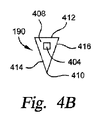
[0047]下部ライナー326は、図4Aに示されるように、第2の部分338の拡大チャネル405に配置された突起部402を含むことができる。突起部402は、分流器190(図1C)を固定するために利用される。図4Bは、本明細書に記載の実施形態による分流器190の底面図である。図4Bに示されるように、分流器190は、底面408と、底面408に形成された凹部404とを含む。分流器190は、下部ライナー326の第2の部分338の拡大チャネル405上に配置され、拡大チャネル405上に形成された突起部402が、下部ライナー326上に分流器190を固定するために、凹部404の内部に嵌合する。分流器190は、ラジカルなどの流体の流れを分割することができる任意の適切な形状を有することができる。一実施形態では、図4Bに示されるように、分流器190は、三角形の形状を有する。別の実施形態では、分流器190は、楕円形の形状を有する。別の実施形態では、分流器190は、円形の形状を有する。分流器190の形状は、分流器190の上方からの見え方に基づいている。分流器190は、高さを有することができる。一実施形態では、分流器190は、シリンダである。別の実施形態では、分流器190は、楕円形のシリンダである。分流器190は、下部ライナー326の第1の部分336に面する第1の端部410と、第1の端部410の反対側の第2の端部412とを有する。第1の端部410は、第2の端部412の幅よりも小さい幅を有することができる。一実施形態では、第1の端部410は、鋭角のエッジである。第1の端部410および第2の端部412は、表面414、416によって接合され得る。一実施形態では、図4Bに示すように、表面414、416のそれぞれが、直線状である。他の実施形態では、表面414、416の1つ以上が、湾曲していてもよい。
[0047]
[0048]図4Cは、本明細書に記載の実施形態によるライナーアセンブリ156の上部ライナー324の斜視図である。図4Cに示されるように、上部ライナー324は、第1の部分340と第2の部分342を含む。第1の部分340は、端部328を含む。一実施形態では、図4Cに示すように、端部328は、半円形であってもよい。端部330(図4A)および端部328は、急激な狭窄のない流体の流れを提供する任意の形状を形成してよい。第2の部分342は、拡大チャネル405と同様の拡大チャネル(図示せず)を含むことができる。一実施形態において、上部ライナー324は、突起部402を含まないことを除いて、下部ライナー326と同一である。分流器190は、下部ライナー326上に配置されたとき、上部ライナー324と接触してもよく、または、分流器190が下部ライナー326上に配置されたとき、間隙が、分流器190と上部ライナー324との間に形成されてもよい。
[0048] Figure 4C is a perspective view of the
[0049]図5は、本明細書に記載の実施形態による図1A~図1Cの処理システム100の一部の断面図である。図5に示すように、処理システム100は、コネクタプレート314を介して処理チャンバ102のチャンバ本体125の第1の側部124に結合されたコネクタ106を含む。コネクタ106は、コネクタプレート314に結合された第1のフランジ310と、遠隔プラズマ源104(図1A)に結合された第2のフランジ312とを含んでもよい。ライナー502が、コネクタ106内に配置され得る。ライナー502は、石英などの耐酸化性の材料から製造されている。ライナー502は、円筒形であってもよく、第1の端部504、第1の端部504の反対側の第2の端部506、および第1の端部504と第2の端部506との間の中央部508を含むことができる。いくつかの実施形態では、ライナー502は、円筒形ではなく、ライナー502は、第1の端部504から第2の端部506へ断面積が拡大してもよい。第1の端部504は、中央部508の壁厚よりも薄い壁厚を有してもよい。第1の端部504は、中央部508の外径よりも小さい外径と、中央部508の内径と同じ内径とを有してもよい。第2の端部506は、中央部508の壁厚よりも薄い壁厚を有してもよい。第2の端部506は、中央部508の外径よりも小さい外径と、中央部508の内径と同じ内径とを有してもよい。ライナー502は、1個の石英を機械加工することにより、または3Dプリンティングにより製造されてもよい。
[0049] FIG. 5 is a cross-sectional view of a portion of the
[0050]カップリングライナー510が、ライナー502に結合されてもよく、カップリングライナー510は、遠隔プラズマ源104の出口カップリングの内側など、遠隔プラズマ源104(図1A)内に配置されてもよい。カップリングライナー510は、円筒形であってもよい。カップリングライナー510は、石英などの耐酸化性の材料から製造されてもよい。カップリングライナー510は、第1の端部512、第1の端部512の反対側の第2の端部514、および第1の端部512と第2の端部514との間の中央部516を含むことができる。第1の端部512は、中央部516の壁厚よりも薄い壁厚を有する。第1の端部512は、中央部516の外径よりも小さい外径と、中央部516の内径と同じ内径とを有する。第2の端部514は、中央部516の壁厚よりも薄い壁厚を有する。第2の端部514は、中央部516の外径よりも小さい外径と、中央部516の内径と同じ内径とを有する。ライナー510の第2の端部514の内径および外径は、それぞれ、ライナー502の第1の端部504の内径および外径と同じであってもよい。カップリングライナー510の第2の端部514は、外部の締め具(図示せず)によってライナー502の第1の端部504に結合されてもよい。カップリングライナー510は、1個の石英を機械加工することにより、または3Dプリンティングにより製造されてもよい。
[0050] A coupling liner 510 may be coupled to
[0051]ライナーアセンブリ156は、ノズル520、およびノズル520と接触しているライナー522を含むことができる。ノズル520およびライナー522は両方とも、石英などの耐酸化性の材料から製造されている。ノズル520およびライナー522のそれぞれが、1個の石英を機械加工することにより、または3Dプリンティングにより製造されてもよい。ノズル520は、チャンバ本体125のスロット202(図2)内に配置され得る。ノズル520は、ライナー502の第2の端部506に結合された端部524を含む。ノズル520の端部524の内径および外径は、それぞれ、ライナー502の第2の端部506の内径および外径と同じであってもよい。ノズル520は、ライナー502に面する第1の開口部532と、第1の開口部532の反対側の第2の開口部534とを含むことができる。第1の開口部532は、ライナー502の第2の端部506の形状に適合する形状を有する。一実施形態では、第2の端部506は、円筒形であり、第1の開口部532は、円形の断面積を有する。第2の開口部534は、ライナー522に形成された開口部の形状に適合する形状を有する。一実施形態では、第2の開口部534は、レーストラック形状を有する。第2の開口部534は、第1の開口部532の断面積と実質的に同じまたはそれより大きい断面積を有する。第1の開口部532および第2の開口部534は、表面526、528、530によって接続され得る。表面526、528、530は、拡大チャネル531を形成する連続的な曲面であってもよい。動作中、遠隔プラズマ源104で形成されたラジカルは、ライナー510、ライナー502、およびライナーアセンブリ156を通って、処理チャンバ102の処理領域146に流入する。ライナー510、502およびライナーアセンブリ156は、石英から製造されているので、ラジカルは、ライナー510、502およびライナーアセンブリ156の表面に接触した時に、再結合しない。加えて、第2の開口部534の断面積は、第1の開口部532の断面積と同じかそれより大きいので、ラジカルの流れは制限されず、処理領域146内のラジカル濃度とフラックスの増加につながる。一実施形態において、ライナー510、502およびライナーアセンブリ156は、処理システム100で使用される。
[0051] The
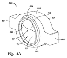
[0052]図6Aは、本明細書に記載の一実施形態によるノズル520の斜視図であり、図6Bは、図6Aのノズル520の断面図である。図6Aおよび図6Bに示されるように、ノズル520は、第1の表面602と、第1の表面602の反対側の第2の表面604とを含む。第1の表面602は、コネクタ106(図5)のライナー502に面してもよく、第2の表面604は、ライナー522(図5)に面してもよい。端部524が、第1の表面602に配置されてもよい。第1の開口部532が、第1の表面602に形成され、第1の開口部532は、図6Aに示されるように、円形の形状を有してもよい。第2の開口部534が、第2の表面604に形成され、第2の開口部534は、レーストラック形状を有してもよい。第2の開口部534は、第1の開口部532の直径より大きい長い寸法と、第1の開口部532の直径より小さい短い寸法とを含むことができる。ノズル520は、第1の端部601、第1の端部601の反対側の第2の端部603、および第1の端部601と第2の端部603との間に位置する部分605を含むことができる。第1の表面602を見たとき、第1および第2の端部601、603は、それぞれ長方形の形状を有することができ、部分605は、楕円形の形状を有することができる。部分605は、図6Aに示される楕円形とは異なる形状を有してもよい。
[0052] Figure 6A is a perspective view of a
[0053]図5、図6Aおよび図6Bに示すように、表面526、528、530、608は、第1の開口部532を第2の開口部534に接続する。第2の開口部534の断面積が、第1の開口部532の断面積と実質的に同じかそれより大きくなるように、表面526、528、530、608は、第1の開口部532の形状から第2の開口部534の形状への移行を容易にする。表面526、528、530、608は、拡大チャネル531を形成する連続的な曲面であってもよい。一実施形態では、拡大チャネル531は、第2の開口部534のレーストラック形状の長い寸法などの1つの寸法において拡大しており、他方、第2の開口部534のレーストラック形状の短い寸法などの別の寸法において減少していてもよい。いくつかの実施形態では、表面526、528、530、608は、異なる曲率を有する別個の表面であってもよい。
[0053] Surfaces 526, 528, 530, 608 connect the
[0054]図7は、本明細書に記載の一実施形態によるライナー522の斜視図である。図7に示されるように、ライナー522は、第1の端部702と、第1の端部702の反対側の第2の端部704とを含む。第1の端部702は、コネクタ106および遠隔プラズマ源104(図1A)に面してもよく、第2の端部704は、処理チャンバ102の処理領域146(図1A)に面してもよい。凹部706が、ノズル520がその中に配置されるように第1の端部702に形成されてもよい。開口部708が、凹部706に形成され、ノズル520の第2の開口部534に結合する。開口部708は、ノズル520の第2の開口部534と同じ形状を有してもよい。一実施形態では、ノズル520の第2の開口部534およびライナー522の開口部708は、両方ともレーストラック断面形状を有する。第2の端部704は、第1のチャンバ壁124(図1A)を越えて延びてもよい。第2の端部704は、部分714を含むことができる。一実施形態では、部分714は、円弧であり、支持リング148(図1A)の一部と実質的に平行である。拡大チャネル712が、ライナー522内に形成され、拡大チャネル712は、開口部708から第2の端部704への流体流路に実質的に垂直な寸法Dにおいて拡大することができる。拡大チャネル712は、ラジカルの流れの狭窄を低減する。1つ以上の締め具(図示せず)がライナー522をチャンバ本体125(図5)に固定するために、1つ以上の開口部710が、ライナー522に形成されてもよい。
[0054] Figure 7 is a perspective view of a
[0055]図8は、本明細書に記載の実施形態による図1A~図1Cの処理システム100の一部の断面側面図である。図8に示すように、処理システム100は、コネクタプレート314を介して処理チャンバ102のチャンバ本体125の第1の側部124に結合されたコネクタ106を含む。コネクタ106は、コネクタプレート314に結合された第1のフランジ310と、遠隔プラズマ源104(図1A)に結合された第2のフランジ312とを含む。ライナー316が、コネクタ106内に配置されて、第1の端部318と、第1の端部318の反対側の第2の端部320とを含むことができる。カップリングライナー302が、ライナー316に結合されてもよく、カップリングライナー302は、遠隔プラズマ源104(図1A)内に配置されてもよい。カップリングライナー302は、ライナー316の第1の端部318にしっかりと嵌合する第2の端部306を含むことができる。
[0055] FIG. 8 is a cross-sectional side view of a portion of the
[0056]ライナーアセンブリ156は、ノズル520、およびノズル520と接触しているライナー522を含むことができる。ノズル520の端部524が、ライナー316の第2の端部320を囲むことができる。端部524は、ライナー316に面する第1の開口部532を形成する。ライナー316の第2の端部320が、第1の開口部532にしっかりと嵌り込むことができるように、ライナー316の第2の端部320の外径は、開口部532よりわずかに小さくてもよい。第2の端部320は、任意の適切な方法で端部524に結合されてよい。第2の開口部534は、ライナー522に形成された開口部708(図7)の形状に適合する形状を有する。動作中、遠隔プラズマ源104で形成されたラジカルは、カップリングライナー302、ライナー316、およびライナーアセンブリ156を通って、処理チャンバ102の処理領域146に流入する。ライナー302、316およびライナーアセンブリ156は、石英などの耐酸化性の材料から製造されているので、ラジカルは、ライナー302、316およびライナーアセンブリ156の表面に接触した時に、再結合しない。加えて、第2の開口部534の断面積は、第1の開口部532の断面積と同じかそれより大きいので、ラジカルの流れは制限されず、処理領域146内のラジカル濃度とフラックスの増加につながる。
[0056] The
[0057]図9Aは、本明細書に記載の実施形態によるライナー522の斜視図である。図9Aに示されるように、ライナー522は、第1の端部702と、第1の端部702の反対側の第2の端部704とを含む。第1の端部702は、コネクタ106および遠隔プラズマ源104(図1A)に面してもよく、第2の端部704は、処理チャンバ102の処理領域146(図1A)に面してもよい。ライナー522は、上面902と、上面902の反対側の底面904とを、さらに含む。拡大チャネル712が、ライナー522内に上面902と底面904との間に形成される。スロット906が、底面904に形成されてもよく、スロット906は、図9Aに示されるように、第2の部分910と第3の部分912との間に位置する第1の部分908を含む。スロット906の第1の部分908は、スロット906の第2の部分910および第3の部分912よりも大きい。
[0057] Figure 9A is a perspective view of a
[0058]図9Bは、本明細書に記載の実施形態による分流器190の斜視図である。図9Bに示すように、分流器190は、第1の端部410、第1の端部410の反対側の第2の端部412、および第1の端部410と第2の端部412を接続する表面414、416を有する。凹部920が、第2の端部412に形成されてもよい。凹部920は、留め具によってライナー522内に分流器190を固定するために利用される。図9Cは、本明細書に記載の実施形態による留め具930の斜視図である。留め具930は、第1の部分932と第2の部分934を含む。第1の部分932は、ライナー522の底面904に形成されたスロット906の第1の部分908に嵌り込むことができる大きさを有する。第1の部分932が、スロット906に固定されるように、第1の部分932の大きさは、スロット906の第2の部分910および第3の部分912よりも大きい。留め具930がスロット906の第1の部分908を通って落下するのを防止するため、第2の部分934が、ライナー522の底面904に載るように、留め具930の第2の部分934は、第1の部分932よりも大きい。第2の部分934は、分流器190の凹部920に嵌り込む大きさである。
[0058] Figure 9B is a perspective view of a
[0059]図10は、本明細書に記載の実施形態による、留め具930によってライナー522に固定された分流器190の斜視図である。図10に示されるように、第1の部分932(図9C)が、ライナー522の底面904に形成されたスロット906の第1の部分908(図9A)に固定されるので、留め具930の第2の部分934は、ライナー522の底面904に固定される。留め具930の第2の部分934が、分流器190の凹部920に嵌り込むので、分流器190は、ライナー522に固定される。図10に示すように、分流器190が処理チャンバ102内に落下するのが、留め具930によって防止されている。ライナー522内の拡大チャネル712が、高さH1を有し、分流器190が、高さH2を有する。分流器190が、ライナー522の拡大チャネル712にしっかりと嵌め込まれることができるように、高さH2は、高さH1よりわずかに小さくてもよい。いくつかの実施形態では、高さH2は、高さH1よりもはるかに小さく、例えば、H1の75パーセント、H1の50パーセント、またはH1の25パーセントなどである。
[0059] FIG. 10 is a perspective view of
[0060]上記は、本開示の実施形態に向けられているが、本開示の基本的な範囲から逸脱することなく、本開示の他のさらなる実施形態を考え出すこともでき、本開示の範囲は、以下の特許請求の範囲によって決定される。 [0060] While the above is directed to embodiments of the present disclosure, other and further embodiments of the present disclosure may be envisioned without departing from the basic scope of the present disclosure, the scope of which is , is determined by the following claims.
Claims (14)
第1の開口部を有する第1の端部と、前記第1の端部の反対側の第2の開口部を有する第2の端部とを備えたノズルであって、前記ノズルの前記第1の開口部は円形の断面を有し、前記ノズルの前記第2の開口部は、前記ノズルの前記第1の開口部よりも広く且つ浅い楕円形の断面を有し、前記ノズルの前記第2の開口部は、前記ノズルの前記第1の開口部の断面積と等しいかまたはそれより大きい断面積を有する、ノズルと、
第1の開口部を有する第1の端部と、前記第1の端部の反対側の第2の開口部を有する第2の端部とを備えたライナーであって、前記ライナーの前記第1の端部は前記ノズルの前記第2の端部に直接結合されており、前記ライナーの前記第2の開口部は、前記ライナーの前記第1の開口部の断面より広い断面を有するが、実質的に高さは同じである、ライナーと、
前記ライナー部材に形成され、前記ノズルの前記第1の端部から前記ライナーの前記第2の端部まで延びるチャネルであって、前記ノズルの前記第1の端部におけるよりも前記ライナーの前記第2の端部においてより広く、前記ノズルの前記第1の端部におけるよりも前記ライナーの前記第2の端部においてより浅いチャネルと、
を備えるライナー部材。 A liner member for a semiconductor processing chamber, comprising:
A nozzle comprising a first end having a first opening and a second end having a second opening opposite said first end, said second end of said nozzle One opening has a circular cross section, the second opening of the nozzle has an elliptical cross section that is wider and shallower than the first opening of the nozzle, and the second opening of the nozzle has an oval cross section that is wider and shallower than the first opening of the nozzle. a nozzle, wherein two openings have a cross-sectional area equal to or greater than the cross-sectional area of the first opening of the nozzle;
A liner comprising a first end having a first opening and a second end having a second opening opposite said first end, said second end of said liner one end is directly connected to said second end of said nozzle, said second opening of said liner having a cross-section wider than that of said first opening of said liner, a liner that is substantially the same height;
A channel formed in the liner member and extending from the first end of the nozzle to the second end of the liner, the channel extending from the first end of the liner to the second end of the liner rather than at the first end of the nozzle. a channel that is wider at two ends and shallower at the second end of the liner than at the first end of the nozzle;
A liner member comprising:
第1の開口部を有する第1の端部と、前記第1の端部の反対側の第2の開口部を有する第2の端部とを備えたコネクタであって、前記コネクタの第2の開口部は、前記コネクタの第1の開口部の断面積と等しいかまたはそれより大きい断面積を有し、前記コネクタの第1の端部はさらに、前記コネクタの前記第1の開口部から半径方向外側に延びる第1のフランジを備え、前記コネクタの第2の端部はさらに、前記コネクタの前記第2の開口部から半径方向外側に延びる第2のフランジを備える、コネクタと、
第1の開口部を有する第1の端部と、前記第1の端部の反対側の第2の開口部を有する第2の端部とを備えたノズルであって、前記ノズルの前記第1の端部は前記コネクタの前記第2の端部に直接結合されており、前記ノズルの前記第1の開口部は円形の断面を有し、前記ノズルの前記第2の開口部は、前記ノズルの前記第1の開口部よりも広く且つ浅い楕円形の断面を有し、前記ノズルの前記第2の開口部は、前記ノズルの前記第1の開口部の断面積と等しいかまたはそれより大きい断面積を有する、ノズルと、
第1の開口部を有する第1の端部と、前記第1の端部の反対側の第2の開口部を有する第2の端部とを備えたライナーであって、前記ライナーの前記第1の端部は前記ノズルの前記第2の端部に直接結合されており、前記ライナーの前記第2の開口部は、前記ライナーの前記第1の開口部の断面より広い断面を有するが、実質的に高さは同じである、ライナーと、
前記ライナーアセンブリを通って形成され、前記コネクタの前記第1の端部から前記ライナーの前記第2の端部まで延びる導管であって、前記導管が、流体流路を画定し、前記流体流路は、前記流体流路の主軸に実質的に垂直な第1の方向に広がり、前記流体流路の主軸および前記第1の方向に実質的に垂直な第2の方向に狭くなる、導管と、
を有する、ライナーアセンブリ。 A liner assembly,
A connector having a first end with a first opening and a second end with a second opening opposite said first end, the second end of said connector has a cross-sectional area equal to or greater than the cross-sectional area of the first opening of the connector, and the first end of the connector further extends from the first opening of the connector. a connector comprising a first radially outwardly extending flange, the second end of the connector further comprising a second flange extending radially outwardly from the second opening of the connector;
A nozzle comprising a first end having a first opening and a second end having a second opening opposite said first end, said second end of said nozzle One end is directly coupled to the second end of the connector, the first opening of the nozzle has a circular cross-section, and the second opening of the nozzle is connected to the having an elliptical cross-section wider and shallower than the first opening of the nozzle, the second opening of the nozzle being equal to or less than the cross-sectional area of the first opening of the nozzle; a nozzle having a large cross-sectional area;
A liner comprising a first end having a first opening and a second end having a second opening opposite said first end, said second end of said liner one end is directly connected to said second end of said nozzle, said second opening of said liner having a cross-section wider than that of said first opening of said liner, a liner that is substantially the same height;
a conduit formed through the liner assembly and extending from the first end of the connector to the second end of the liner, the conduit defining a fluid flow path; widens in a first direction substantially perpendicular to the major axis of the fluid flow channel and narrows in a second direction substantially perpendicular to the major axis of the fluid channel and the first direction;
a liner assembly.
コネクタによって前記処理チャンバに結合された遠隔プラズマ源、
を備える処理システムであって、
前記処理チャンバは、
基板支持部、
前記基板支持部に結合されたチャンバ本体であって、前記チャンバ本体が、第1の側部および前記第1の側部の反対側の第2の側部を備え、前記チャンバ本体および前記基板支持部が、協働して処理容積部を画定する、チャンバ本体、
前記第2の側部に隣接して前記基板支持部に配置された分散ポンピング構造、および
前記第1の側部に配置されたライナーアセンブリ、
を備え、前記ライナーアセンブリは、
第1の開口部を有する第1の端部と、前記第1の端部の反対側の第2の開口部を有する第2の端部とを備えたノズルであって、前記ノズルの前記第1の開口部は円形の断面を有し、前記ノズルの前記第2の開口部は、前記ノズルの前記第1の開口部よりも広く且つ浅い楕円形の断面を有し、前記ノズルの前記第2の開口部は、前記ノズルの前記第1の開口部の断面積と等しいかまたはそれより大きい断面積を有する、ノズル、および
第1の開口部を有する第1の端部と、前記第1の端部の反対側の第2の開口部を有する第2の端部とを備えたライナーであって、前記ライナーの前記第1の端部は前記ノズルの前記第2の端部に直接結合されており、前記ライナーの前記第2の開口部は、前記ライナーの前記第1の開口部の断面より広い断面を有するが、実質的に高さは同じである、ライナー、
を備え、
前記コネクタは、第1の開口部を有する第1の端部と、前記第1の端部の反対側の第2の開口部を有する第2の端部とを備え、前記コネクタの第2の開口部は、前記コネクタの第1の開口部の断面積と等しいかまたはそれより大きい断面積を有し、前記コネクタの前記第2の端部は、前記ライナーアセンブリの前記ノズルの前記第1の端部に接続されて、前記遠隔プラズマ源から前記処理容積部までの流体流路を形成し、前記流体流路は、前記流体流路の主軸に実質的に垂直な第1の方向に広がり、前記流体流路の主軸および前記第1の方向に実質的に垂直な第2の方向に狭くなる、処理システム。 a processing chamber, and a remote plasma source coupled to the processing chamber by a connector;
A processing system comprising:
The processing chamber comprises:
substrate support,
A chamber body coupled to the substrate support, the chamber body comprising a first side and a second side opposite the first side, the chamber body and the substrate support a chamber body, the portions cooperatively defining a processing volume;
a distributed pumping structure positioned on the substrate support adjacent the second side; and a liner assembly positioned on the first side;
wherein the liner assembly comprises:
A nozzle comprising a first end having a first opening and a second end having a second opening opposite said first end, said second end of said nozzle One opening has a circular cross section, the second opening of the nozzle has an elliptical cross section that is wider and shallower than the first opening of the nozzle, and the second opening of the nozzle has an oval cross section that is wider and shallower than the first opening of the nozzle. a nozzle, wherein two openings have a cross-sectional area equal to or greater than the cross-sectional area of said first opening of said nozzle; and a first end having a first opening; and a second end having a second opening opposite the end of the liner, wherein the first end of the liner is directly coupled to the second end of the nozzle wherein said second opening of said liner has a cross-section that is wider than the cross-section of said first opening of said liner but is substantially the same height;
with
The connector has a first end with a first opening and a second end with a second opening opposite the first end, and the second end of the connector has a second opening. The opening has a cross-sectional area equal to or greater than the cross-sectional area of the first opening of the connector, and the second end of the connector connects to the first opening of the nozzle of the liner assembly. connected to an end to define a fluid flow path from said remote plasma source to said processing volume, said fluid flow path extending in a first direction substantially perpendicular to a major axis of said fluid flow path; A treatment system, wherein the main axis of the fluid flow path narrows in a second direction substantially perpendicular to the first direction.
Applications Claiming Priority (3)
| Application Number | Priority Date | Filing Date | Title |
|---|---|---|---|
| US201762513200P | 2017-05-31 | 2017-05-31 | |
| US62/513,200 | 2017-05-31 | ||
| PCT/US2018/024539 WO2018222256A1 (en) | 2017-05-31 | 2018-03-27 | Remote plasma oxidation chamber |
Publications (3)
| Publication Number | Publication Date |
|---|---|
| JP2020522132A JP2020522132A (en) | 2020-07-27 |
| JP2020522132A5 JP2020522132A5 (en) | 2021-05-06 |
| JP7125427B2 true JP7125427B2 (en) | 2022-08-24 |
Family
ID=64455931
Family Applications (1)
| Application Number | Title | Priority Date | Filing Date |
|---|---|---|---|
| JP2019564957A Active JP7125427B2 (en) | 2017-05-31 | 2018-03-27 | Remote plasma oxidation chamber |
Country Status (6)
| Country | Link |
|---|---|
| US (1) | US11615944B2 (en) |
| JP (1) | JP7125427B2 (en) |
| KR (2) | KR102509014B1 (en) |
| CN (1) | CN110612593B (en) |
| TW (1) | TWI798210B (en) |
| WO (1) | WO2018222256A1 (en) |
Families Citing this family (6)
| Publication number | Priority date | Publication date | Assignee | Title |
|---|---|---|---|---|
| USD882536S1 (en) * | 2017-04-28 | 2020-04-28 | Applied Materials, Inc. | Plasma source liner |
| US10847337B2 (en) | 2018-01-24 | 2020-11-24 | Applied Materials, Inc. | Side inject designs for improved radical concentrations |
| CN113196444A (en) * | 2018-12-20 | 2021-07-30 | 应用材料公司 | Method and apparatus for supplying improved gas flow to a processing volume of a processing chamber |
| US20220223383A1 (en) * | 2019-04-05 | 2022-07-14 | Applied Materials, Inc. | Process system with variable flow valve |
| KR20210094694A (en) * | 2020-01-21 | 2021-07-30 | 삼성전자주식회사 | Substrate processing apparatus, material layer deposition apparatus, and apparatus for atmospheric pressure chemical vapor deposition |
| KR102522687B1 (en) * | 2020-10-20 | 2023-04-18 | 에이피시스템 주식회사 | Thin film processing apparatus |
Citations (11)
| Publication number | Priority date | Publication date | Assignee | Title |
|---|---|---|---|---|
| JP2001118799A (en) | 1999-10-22 | 2001-04-27 | Matsushita Electric Ind Co Ltd | Method and device for controlling introduction and flow of gas |
| JP2002151486A (en) | 2000-10-30 | 2002-05-24 | Applied Materials Inc | Substrate processing method and device thereof, and operation method for substrate processor |
| US20020073925A1 (en) | 1999-04-22 | 2002-06-20 | David B. Noble | Apparatus and method for exposing a substrate to plasma radicals |
| JP2002217187A (en) | 2001-01-18 | 2002-08-02 | Tokyo Electron Ltd | Plasma system and method of plasma production |
| JP2004091848A (en) | 2002-08-30 | 2004-03-25 | Tokyo Electron Ltd | Gaseous raw material supply system for thin film forming apparatus and thin film forming apparatus |
| JP2007157885A (en) | 2005-12-02 | 2007-06-21 | Mitsui Eng & Shipbuild Co Ltd | Material gas supply apparatus |
| JP2008091938A (en) | 1996-07-15 | 2008-04-17 | Applied Materials Inc | Process kit, wafer processing device, and method for heating process kit |
| US20090110826A1 (en) | 2007-10-25 | 2009-04-30 | Asm America, Inc. | Reaction apparatus having multiple adjustable exhaust ports |
| JP2012089863A (en) | 2005-01-18 | 2012-05-10 | Asm America Inc | Reaction system for growing thin film |
| WO2013051248A1 (en) | 2011-10-07 | 2013-04-11 | 東京エレクトロン株式会社 | Plasma processing apparatus |
| US20130168377A1 (en) | 2011-12-29 | 2013-07-04 | Stmicroelectronics Pte Ltd. | Adapter for coupling a diffusion furnace system |
Family Cites Families (12)
| Publication number | Priority date | Publication date | Assignee | Title |
|---|---|---|---|---|
| JPH0729827A (en) | 1993-07-13 | 1995-01-31 | Kawasaki Steel Corp | Method and system for fabricating semiconductor substrate |
| US5620523A (en) * | 1994-04-11 | 1997-04-15 | Canon Sales Co., Inc. | Apparatus for forming film |
| US5935334A (en) * | 1996-11-13 | 1999-08-10 | Applied Materials, Inc. | Substrate processing apparatus with bottom-mounted remote plasma system |
| US6576564B2 (en) * | 2000-12-07 | 2003-06-10 | Micron Technology, Inc. | Photo-assisted remote plasma apparatus and method |
| EP1310466A3 (en) * | 2001-11-13 | 2003-10-22 | Tosoh Corporation | Quartz glass parts, ceramic parts and process of producing those |
| US20070051471A1 (en) * | 2002-10-04 | 2007-03-08 | Applied Materials, Inc. | Methods and apparatus for stripping |
| US20050221618A1 (en) * | 2004-03-31 | 2005-10-06 | Amrhein Frederick J | System for controlling a plenum output flow geometry |
| JP4572100B2 (en) * | 2004-09-28 | 2010-10-27 | 日本エー・エス・エム株式会社 | Plasma processing equipment |
| CN103189957B (en) * | 2010-10-05 | 2016-01-20 | 欧瑞康先进科技股份公司 | Original position for vacuum processable polymer substrate regulates |
| US10225919B2 (en) | 2011-06-30 | 2019-03-05 | Aes Global Holdings, Pte. Ltd | Projected plasma source |
| KR102376982B1 (en) | 2015-04-14 | 2022-03-21 | 삼성전자주식회사 | Remote plasma generator for reducing particles by using ceramic |
| KR101692697B1 (en) * | 2015-04-21 | 2017-01-04 | (주)뉴젠텍 | A Remote Plasma Source Block with Align Key |
-
2018
- 2018-03-27 KR KR1020197038362A patent/KR102509014B1/en active IP Right Grant
- 2018-03-27 CN CN201880029034.XA patent/CN110612593B/en active Active
- 2018-03-27 JP JP2019564957A patent/JP7125427B2/en active Active
- 2018-03-27 US US15/937,076 patent/US11615944B2/en active Active
- 2018-03-27 KR KR1020237008095A patent/KR20230047477A/en active IP Right Grant
- 2018-03-27 WO PCT/US2018/024539 patent/WO2018222256A1/en active Application Filing
- 2018-03-30 TW TW107111093A patent/TWI798210B/en active
Patent Citations (11)
| Publication number | Priority date | Publication date | Assignee | Title |
|---|---|---|---|---|
| JP2008091938A (en) | 1996-07-15 | 2008-04-17 | Applied Materials Inc | Process kit, wafer processing device, and method for heating process kit |
| US20020073925A1 (en) | 1999-04-22 | 2002-06-20 | David B. Noble | Apparatus and method for exposing a substrate to plasma radicals |
| JP2001118799A (en) | 1999-10-22 | 2001-04-27 | Matsushita Electric Ind Co Ltd | Method and device for controlling introduction and flow of gas |
| JP2002151486A (en) | 2000-10-30 | 2002-05-24 | Applied Materials Inc | Substrate processing method and device thereof, and operation method for substrate processor |
| JP2002217187A (en) | 2001-01-18 | 2002-08-02 | Tokyo Electron Ltd | Plasma system and method of plasma production |
| JP2004091848A (en) | 2002-08-30 | 2004-03-25 | Tokyo Electron Ltd | Gaseous raw material supply system for thin film forming apparatus and thin film forming apparatus |
| JP2012089863A (en) | 2005-01-18 | 2012-05-10 | Asm America Inc | Reaction system for growing thin film |
| JP2007157885A (en) | 2005-12-02 | 2007-06-21 | Mitsui Eng & Shipbuild Co Ltd | Material gas supply apparatus |
| US20090110826A1 (en) | 2007-10-25 | 2009-04-30 | Asm America, Inc. | Reaction apparatus having multiple adjustable exhaust ports |
| WO2013051248A1 (en) | 2011-10-07 | 2013-04-11 | 東京エレクトロン株式会社 | Plasma processing apparatus |
| US20130168377A1 (en) | 2011-12-29 | 2013-07-04 | Stmicroelectronics Pte Ltd. | Adapter for coupling a diffusion furnace system |
Also Published As
| Publication number | Publication date |
|---|---|
| JP2020522132A (en) | 2020-07-27 |
| KR102509014B1 (en) | 2023-03-13 |
| TW201907044A (en) | 2019-02-16 |
| TWI798210B (en) | 2023-04-11 |
| CN110612593A (en) | 2019-12-24 |
| CN110612593B (en) | 2022-09-13 |
| US20180347045A1 (en) | 2018-12-06 |
| KR20200003426A (en) | 2020-01-09 |
| US11615944B2 (en) | 2023-03-28 |
| KR20230047477A (en) | 2023-04-07 |
| WO2018222256A1 (en) | 2018-12-06 |
Similar Documents
| Publication | Publication Date | Title |
|---|---|---|
| JP7125427B2 (en) | Remote plasma oxidation chamber | |
| US11608559B2 (en) | Integrated showerhead with thermal control for delivering radical and precursor gas to a downstream chamber to enable remote plasma film deposition | |
| TWI677593B (en) | Apparatus and method for providing a uniform flow of gas | |
| KR102110610B1 (en) | Dual plenum, axi-symmetric showerhead with edge-to-center gas delivery | |
| JP2017226863A (en) | Gas mixer, and substrate treatment apparatus | |
| TW201840948A (en) | Gas distribution apparatus and processing chamber for providing uniform flow of gas | |
| JP2019537267A (en) | Design of a two-zone flow cooling plate with concentric or spiral channels for efficient gas distribution assembly cooling | |
| KR20230169367A (en) | Apparatus for multi-flow precursor dosage | |
| TWI682489B (en) | Substrate support with multiple heating zones | |
| TW202243085A (en) | Showerhead with air-gapped plenums and overhead isolation gas distributor | |
| JP7387794B2 (en) | Dogbone inlet cone profile for remote plasma oxidation chamber | |
| TW201611155A (en) | Reactor of substrate processing apparatus | |
| TWI762897B (en) | Process system with variable flow valve | |
| TW202113912A (en) | Gas adjusting device and plasma etching equipment applying same | |
| TWI722451B (en) | Support assembly and chamber using the same | |
| WO2023182031A1 (en) | Substrate-processing apparatus and substrate-processing method | |
| US20230087913A1 (en) | Coolant channel with internal fins for substrate processing pedestals | |
| TW202320120A (en) | Substrate supports with mesochannel assemblies | |
| KR20220137990A (en) | Cooling plate for semiconductor processing chamber windows | |
| TW202342786A (en) | Dual pressure oxidation method for forming an oxide layer in a feature | |
| KR20230022212A (en) | Pedestal thermal profile tuning using multiple heated zones and thermal voids | |
| KR20200098739A (en) | Atomic layer deposition chamber with thermal lid | |
| JP2010084184A (en) | Substrate treatment apparatus |
Legal Events
| Date | Code | Title | Description |
|---|---|---|---|
| A521 | Request for written amendment filed |
Free format text: JAPANESE INTERMEDIATE CODE: A523 Effective date: 20210326 |
|
| A621 | Written request for application examination |
Free format text: JAPANESE INTERMEDIATE CODE: A621 Effective date: 20210326 |
|
| A977 | Report on retrieval |
Free format text: JAPANESE INTERMEDIATE CODE: A971007 Effective date: 20220316 |
|
| A131 | Notification of reasons for refusal |
Free format text: JAPANESE INTERMEDIATE CODE: A131 Effective date: 20220329 |
|
| A521 | Request for written amendment filed |
Free format text: JAPANESE INTERMEDIATE CODE: A523 Effective date: 20220623 |
|
| TRDD | Decision of grant or rejection written | ||
| A01 | Written decision to grant a patent or to grant a registration (utility model) |
Free format text: JAPANESE INTERMEDIATE CODE: A01 Effective date: 20220712 |
|
| A61 | First payment of annual fees (during grant procedure) |
Free format text: JAPANESE INTERMEDIATE CODE: A61 Effective date: 20220812 |
|
| R150 | Certificate of patent or registration of utility model |
Ref document number: 7125427 Country of ref document: JP Free format text: JAPANESE INTERMEDIATE CODE: R150 |