以下、図面を参照しながら、本開示の実施形態を詳細に説明する。以下の実施形態は、例示であり、本開示による発光装置および発光モジュールは、以下の実施形態に限られない。例えば、以下の実施形態で示される数値、形状、材料、ステップ、そのステップの順序などは、あくまでも一例であり、技術的に矛盾が生じない限りにおいて種々の改変が可能である。
Hereinafter, embodiments of the present disclosure will be described in detail with reference to the drawings. The following embodiments are examples, and the light-emitting device and light-emitting module according to the present disclosure are not limited to the following embodiments. For example, numerical values, shapes, materials, steps, order of steps, and the like shown in the following embodiments are merely examples, and various modifications are possible as long as there is no technical contradiction.
図面が示す構成要素の寸法、形状等は、わかり易さのために誇張されている場合があり、実際の発光装置または発光モジュールにおける寸法、形状および構成要素間の大小関係を反映していない場合がある。また、図面が過度に複雑になることを避けるために、一部の要素の図示を省略することがある。
The dimensions, shapes, etc. of components shown in the drawings may be exaggerated for clarity, and may not reflect the dimensions, shapes, and size relationships between components in the actual light-emitting device or light-emitting module. be. Also, some elements may be omitted to avoid over-complicating the drawing.
以下の説明において、実質的に同じ機能を有する構成要素は共通の参照符号で示し、説明を省略することがある。以下の説明では、特定の方向または位置を示す用語(例えば、「上」、「下」、「右」、「左」およびそれらの用語を含む別の用語)を用いる場合がある。しかしながら、それらの用語は、参照した図面における相対的な方向または位置をわかり易さのために用いているに過ぎない。参照した図面における「上」、「下」等の用語による相対的な方向または位置の関係が同一であれば、本開示以外の図面、実際の製品、製造装置等において、参照した図面と同一の配置でなくてもよい。本開示において「平行」とは、特に他の言及がない限り、2つの直線、辺、面等が0°から±5°程度の範囲にある場合を含む。また、本開示において「垂直」または「直交」とは、特に他の言及がない限り、2つの直線、辺、面等が90°から±5°程度の範囲にある場合を含む。
In the following description, constituent elements having substantially the same functions are denoted by common reference numerals, and their description may be omitted. The following description may use terms (eg, "upper", "lower", "right", "left" and other terms that include those terms) that indicate particular directions or positions. However, these terms are used only for clarity of relative orientation or position in the referenced drawings. If the relative direction or positional relationship of terms such as “upper” and “lower” in the referenced drawings is the same, drawings other than the present disclosure, actual products, manufacturing equipment, etc. are the same as the referenced drawings. It does not have to be placement. In the present disclosure, “parallel” includes cases where two straight lines, sides, planes, etc. are in the range of about 0° to ±5°, unless otherwise specified. In the present disclosure, "perpendicular" or "perpendicular" includes cases where two straight lines, sides, planes, etc. are in the range of about 90° to ±5° unless otherwise specified.
(第1の実施形態)
図1は、本開示の第1の実施形態による発光装置の例示的な構成を示す。図1に示す発光装置200は、上面210aを有する導光板210と、導光板210の下方に位置する層状の光反射性部材220とを含む。なお、図1には、説明の便宜のために、互いに直交するX方向、Y方向およびZ方向を示す矢印があわせて図示されている。本開示の他の図面においてもこれらの方向を示す矢印を図示することがある。
(First embodiment)
FIG. 1 shows an exemplary configuration of a light emitting device according to a first embodiment of the present disclosure. The light emitting device 200 shown in FIG. 1 includes a light guide plate 210 having an upper surface 210 a and a layered light reflecting member 220 positioned below the light guide plate 210 . For convenience of explanation, FIG. 1 also shows arrows indicating the X, Y, and Z directions that are orthogonal to each other. Arrows indicating these directions may also be illustrated in other drawings of the present disclosure.
後に詳しく説明するように、本開示の実施形態による発光装置は、各々が少なくとも1つの発光素子を含む複数の単位の繰り返し構造を有する。以下では、説明の便宜のために、発光素子を有する単位の各々を発光セルと呼ぶことがある。
As described in detail below, light-emitting devices according to embodiments of the present disclosure have a repeating structure of multiple units each including at least one light-emitting element. Hereinafter, each unit having a light-emitting element may be referred to as a light-emitting cell for convenience of explanation.
図1に例示する構成において、発光装置200は、合計16個の矩形状の発光セル100Uを含む。ここでは、これら発光セル100Uは、4行4列のマトリクス状に配列されている。発光装置200に含まれる発光セル100Uの数およびそれら発光セル100Uの配置は、任意であり、図1に示す構成に限定されない。各発光セル100Uは、導光板210の一部および光反射性部材220の一部を含む。
In the configuration illustrated in FIG. 1, the light emitting device 200 includes a total of 16 rectangular light emitting cells 100U. Here, these light emitting cells 100U are arranged in a matrix of 4 rows and 4 columns. The number of light emitting cells 100U included in light emitting device 200 and the arrangement of these light emitting cells 100U are arbitrary, and are not limited to the configuration shown in FIG. Each light emitting cell 100U includes part of the light guide plate 210 and part of the light reflecting member 220 .
導光板210は、上面210a側に複数の光拡散構造を有する。これら光拡散構造は、発光セル100Uに対応して設けられる。換言すれば、複数の発光セル100Uの各々は、導光板210の上面210a側に位置する光拡散構造を有する。ここでは、複数の光拡散構造は、複数の凹部12の形で各発光セル100Uに設けられている。発光セル100Uが4行4列に配列されていることに対応して、複数の凹部12も二次元の配列を有する。すなわち、ここでは、導光板210の光拡散構造としての複数の凹部12は、上面210aにおいて4行4列の二次元配列を有する。しかしながら、図1に示す光拡散構造の配置は、あくまでも例示であり、例えば、発光セル100Uが1行m列(またはn行1列)に配列されていることに対応して複数の凹部12が直線状に並ぶこともあり得る。
The light guide plate 210 has a plurality of light diffusion structures on the upper surface 210a side. These light diffusion structures are provided corresponding to the light emitting cells 100U. In other words, each of the plurality of light emitting cells 100U has a light diffusing structure positioned on the upper surface 210a side of the light guide plate 210 . Here, multiple light diffusing structures are provided in each light emitting cell 100U in the form of multiple recesses 12 . The recesses 12 also have a two-dimensional arrangement corresponding to the arrangement of the light emitting cells 100U in 4 rows and 4 columns. That is, here, the plurality of recesses 12 as the light diffusion structure of the light guide plate 210 has a two-dimensional array of 4 rows and 4 columns on the upper surface 210a. However, the arrangement of the light diffusion structure shown in FIG. 1 is merely an example, and for example, a plurality of concave portions 12 are arranged in correspondence with the light emitting cells 100U being arranged in 1 row and m columns (or n rows and 1 column). They can also be arranged in a straight line.
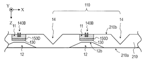
図2は、発光セル100Uの例示的な構成を模式的に示す。図2に示す発光セル100Aは、上述の発光セル100Uの一例である。図2は、導光板210の上面210aに垂直に発光セル100Aを切断したときの断面を模式的に示している。図示するように、発光セル100Aは、上面110aおよび上面110aとは反対側に位置する下面110bを有する導光板110と、導光板110の下面110b側に位置する光反射性部材120とを含む。導光板110および光反射性部材120は、それぞれ、図1を参照して説明した導光板210の一部および光反射性部材220の一部である。なお、図2に例示する構成において、光反射性部材120は、導光板110の下面110bを覆う層状の基部120mと、基部120mから導光板110の上面110aに向かって立ち上がる壁部120wとを含む。
FIG. 2 schematically shows an exemplary configuration of the light emitting cell 100U. A light-emitting cell 100A shown in FIG. 2 is an example of the above-described light-emitting cell 100U. FIG. 2 schematically shows a cross section when the light emitting cell 100A is cut perpendicular to the upper surface 210a of the light guide plate 210. As shown in FIG. As shown, the light emitting cell 100A includes a light guide plate 110 having an upper surface 110a and a lower surface 110b located opposite to the upper surface 110a, and a light reflecting member 120 located on the lower surface 110b side of the light guide plate 110. Light guide plate 110 and light reflective member 120 are part of light guide plate 210 and light reflective member 220 described with reference to FIG. 1, respectively. 2, the light reflecting member 120 includes a layered base portion 120m covering the lower surface 110b of the light guide plate 110, and a wall portion 120w rising from the base portion 120m toward the upper surface 110a of the light guide plate 110. .
図示するように、発光セル100Aは、さらに、光反射性樹脂層130と、発光素子140Aと、波長変換部材150Aと、光反射性部材120上の配線層160とを含む。以下、発光セル100Aの各構成要素をより詳細に説明する。
As shown, the light emitting cell 100A further includes a light reflecting resin layer 130, a light emitting element 140A, a wavelength converting member 150A, and a wiring layer 160 on the light reflecting member 120. FIG. Each component of the light emitting cell 100A will be described in more detail below.
[導光板110]
導光板110は、アクリル、ポリカーボネート、環状ポリオレフィン、ポリエチレンテレフタレート、ポリエステル等の熱可塑性樹脂、エポキシ、シリコーン等の熱硬化性樹脂、または、ガラスから形成される概ね板状の部材であり、透光性を有する。これらの材料のうち、特に、ポリカーボネートは、安価でありながら、高い透明度を得ることが可能である。なお、本明細書における「透光性」および「透光」の用語は、入射した光に対して拡散性を示すことをも包含するように解釈され、「透明」であることに限定されない。導光板110は、例えば母材とは異なる屈折率を有する材料が分散させられることにより、光拡散機能を有していてもよい。
[Light guide plate 110]
The light guide plate 110 is a generally plate-shaped member made of thermoplastic resin such as acrylic, polycarbonate, cyclic polyolefin, polyethylene terephthalate, polyester, thermosetting resin such as epoxy or silicone, or glass. have Among these materials, polycarbonate, in particular, can provide high transparency while being inexpensive. The terms “translucent” and “translucent” in this specification are interpreted to include the ability to diffuse incident light, and are not limited to being “transparent”. The light guide plate 110 may have a light diffusion function, for example, by dispersing a material having a refractive index different from that of the base material.
導光板110は、後述する発光素子140Aからの光を拡散させて上面110aから出射させる機能を有する。導光板110の上面110aは、上述の上面210aの一部である。すなわち、本実施形態において、上面110aの集合は、発光装置200において光が出射される発光面を構成する。
The light guide plate 110 has a function of diffusing light from the light emitting elements 140A described later and emitting the light from the upper surface 110a. The top surface 110a of the light guide plate 110 is part of the top surface 210a described above. That is, in the present embodiment, the set of upper surfaces 110a constitutes a light-emitting surface from which light is emitted in the light-emitting device 200. FIG.
導光板110は、上面110aに光拡散構造を有する。光拡散構造は、発光素子140Aから出射されて導光板110に入射した光を例えば空気層との界面で反射させて導光板110の面内に拡散させる。導光板110の上面110aに光拡散構造を設けることによ
り、上面110aのうち、発光素子140Aの直上以外の領域における輝度が向上し、導光板の上面110a、換言すれば、発光セル100Aの上面における輝度ムラを効果的に抑制し得る。すなわち、光拡散構造は、導光板110の薄化に貢献する。導光板110の厚さは、典型的には、0.1mm以上5mm以下程度であり、特に、本開示の実施形態によれば、0.5mm以上3mm以下程度の範囲とすることも可能である。
The light guide plate 110 has a light diffusion structure on the upper surface 110a. The light diffusing structure reflects the light emitted from the light emitting element 140A and incident on the light guide plate 110 at the interface with the air layer, for example, and diffuses the light within the plane of the light guide plate 110 . By providing the light diffusion structure on the upper surface 110a of the light guide plate 110, the luminance in the area of the upper surface 110a other than directly above the light emitting elements 140A is improved, and the brightness of the upper surface 110a of the light guide plate, in other words, on the upper surface of the light emitting cell 100A is improved. Brightness unevenness can be effectively suppressed. That is, the light diffusion structure contributes to thinning the light guide plate 110 . The thickness of the light guide plate 110 is typically about 0.1 mm or more and 5 mm or less, and in particular, according to the embodiment of the present disclosure, it can be set to a range of about 0.5 mm or more and 3 mm or less. .
図2に例示する構成において、光拡散構造は、底面12bおよび側面12cを含む逆円錐台形状の凹部12の形で導光板110の上面110aに設けられている。凹部12は、導光板110の内部を上面110aに向かって進行する光を傾斜面である側面12cと空気層との界面で反射させる。底面12bおよび側面12cの断面視における形状は、図示するような直線状に限定されず、曲線状であってもよいし、屈曲、段差を含む形状であってもよい。導光板110本体の材料とは屈折率の異なる材料で凹部12の内部が充填されていてもよい。あるいは、底面12b上および側面12c上に、金属等の反射膜、白色樹脂層等の光反射性の部材が配置されていてもよい。
In the configuration illustrated in FIG. 2, the light diffusing structure is provided on the top surface 110a of the light guide plate 110 in the form of an inverted truncated conical recess 12 including a bottom surface 12b and a side surface 12c. The concave portion 12 reflects light traveling toward the upper surface 110a inside the light guide plate 110 at the interface between the inclined side surface 12c and the air layer. The cross-sectional shape of the bottom surface 12b and the side surface 12c is not limited to a linear shape as shown in the figure, and may be a curved shape or a shape including bends and steps. The interior of the concave portion 12 may be filled with a material having a different refractive index from the material of the light guide plate 110 main body. Alternatively, a light-reflective member such as a reflective film made of metal or the like, a white resin layer, or the like may be arranged on the bottom surface 12b and the side surface 12c.
光拡散構造の具体的な構成は、図2に示す凹部12のような構造に限定されない。光拡散構造の具体的な構成は、導光板110の下面110b側に配置される発光素子の形状および特性等に応じて適宜に決定され得る。また、光拡散構造を凹部の形とする場合であっても、凹部の形状は、逆円錐台形状に限定されず、所望の光学特性に応じて適宜変更され得る。凹部12の形状は、例えば、円錐、または、四角錐、六角錐等の多角錐形状、あるいは多角錐台形状等であってもよい。凹部12の深さは、例えば、0.05mm以上3mm以下の範囲である。光拡散構造として、凹部に代えて、上面110aから突出する凸部が適用されることもあり得る。
A specific configuration of the light diffusing structure is not limited to a structure like the concave portion 12 shown in FIG. A specific configuration of the light diffusing structure can be appropriately determined according to the shape and characteristics of the light emitting elements arranged on the lower surface 110b side of the light guide plate 110 . Moreover, even when the light diffusion structure is formed in the shape of a concave portion, the shape of the concave portion is not limited to an inverted truncated cone shape, and can be appropriately changed according to desired optical characteristics. The shape of the concave portion 12 may be, for example, a cone, a polygonal pyramid shape such as a quadrangular pyramid or a hexagonal pyramid, or a polygonal truncated pyramid shape. The depth of the concave portion 12 is, for example, in the range of 0.05 mm or more and 3 mm or less. As the light diffusing structure, instead of the concave portion, a convex portion projecting from the upper surface 110a may be applied.
導光板110は、単層であってもよく、複数の透光性の層を含む積層構造を有していてもよい。複数の透光性の層を積層する場合には、任意の層間に空気層等の、他とは屈折率の異なる層を介在させてもよい。積層構造の任意の層間に例えば空気層を介在させることにより、発光素子140Aからの光をより拡散させやすくなり、輝度ムラをより低減し得る。
Light guide plate 110 may be a single layer or may have a laminated structure including a plurality of translucent layers. When laminating a plurality of translucent layers, a layer having a refractive index different from that of the others, such as an air layer, may be interposed between arbitrary layers. By interposing, for example, an air layer between arbitrary layers of the laminated structure, the light from the light emitting element 140A can be diffused more easily, and luminance unevenness can be further reduced.
導光板110は、さらに、下面110b側に凹部11を有する。図2に例示する構成において、発光素子140Aの一部、光反射性樹脂層130および波長変換部材150Aは、凹部11の内部に位置している。図2から理解されるように、典型的には、凹部11は、上述の複数の凹部12のうちの対応する1つの直下に位置する。すなわち、ここでは、導光板210の上面210aが二次元に配列された複数の光拡散構造を有することに対応して、導光板210の上面210aとは反対側の主面(下面)は、二次元に配列された複数の凹部12を有する。もちろん、光拡散構造の配置によっては、導光板210の下面側に凹部12が例えば一列に並ぶこともあり得る。
The light guide plate 110 further has a recess 11 on the lower surface 110b side. In the configuration illustrated in FIG. 2 , a portion of the light emitting element 140A, the light reflecting resin layer 130 and the wavelength conversion member 150A are positioned inside the recess 11 . As can be seen from FIG. 2, typically the recess 11 is located directly below a corresponding one of the plurality of recesses 12 described above. That is, here, in response to the fact that the upper surface 210a of the light guide plate 210 has a plurality of light diffusion structures arranged two-dimensionally, the main surface (lower surface) of the light guide plate 210 opposite to the upper surface 210a has two It has a plurality of recesses 12 that are dimensionally arranged. Of course, depending on the arrangement of the light diffusion structure, the concave portions 12 may be arranged in a row on the lower surface side of the light guide plate 210, for example.
図3は、導光板210の上面210aの法線方向から発光セル100Aを見たときの外観の一例を示す。図3に例示する構成において、発光セル100Aは、正方形状の外形を有する。したがって、発光セル100Aの導光板110の集合体としての導光板210も、全体として矩形状を有する。ここでは、上述のX方向およびY方向は、導光板210の矩形状の互いに直交する辺の一方および他方にそれぞれ一致している(図1参照)。
FIG. 3 shows an example of the appearance when the light emitting cell 100A is viewed from the normal direction of the upper surface 210a of the light guide plate 210. As shown in FIG. In the configuration illustrated in FIG. 3, the light emitting cell 100A has a square outline. Therefore, light guide plate 210 as an aggregate of light guide plates 110 of light emitting cell 100A also has a rectangular shape as a whole. Here, the X direction and the Y direction described above correspond to one side and the other side of the rectangular shape of the light guide plate 210, which are orthogonal to each other, respectively (see FIG. 1).
発光装置200の発光面を構成する、導光板210の上面210aの矩形状の一辺の長さは、例えば1cm以上200cm以下の範囲であり得る。本開示の典型的な実施形態では、導光板210の上面210aの矩形状の一辺は、20mm以上25mm以下の長さを有する。
The length of one side of the rectangular shape of the upper surface 210a of the light guide plate 210, which constitutes the light emitting surface of the light emitting device 200, can be, for example, in the range of 1 cm or more and 200 cm or less. In a typical embodiment of the present disclosure, one rectangular side of the upper surface 210a of the light guide plate 210 has a length of 20 mm or more and 25 mm or less.
図3に示す例において、導光板110の下面110b側に設けられる凹部11は、正方形状の外形を有する。すなわち、この例では、凹部11は、四角柱形状の穴部である。このように、凹部11は、導光板110の外形に相似な外形を有し得る。典型的には、導光板110の下面110b側に位置する第1凹部としての凹部11の中心と、上面110a側に位置する第2凹部としての凹部12の中心とは、概ね一致させられる。
In the example shown in FIG. 3, the recess 11 provided on the lower surface 110b side of the light guide plate 110 has a square shape. That is, in this example, the recessed portion 11 is a rectangular prism-shaped hole. Thus, the concave portion 11 can have an outer shape similar to the outer shape of the light guide plate 110 . Typically, the center of the concave portion 11 as the first concave portion located on the lower surface 110b side of the light guide plate 110 and the center of the concave portion 12 as the second concave portion located on the upper surface 110a side are substantially aligned.
図3に示す、凹部11の矩形状の底面(あるいは開口)の対角線方向に沿った長さは、例えば、0.05mm以上10mm以下とすることができ、好ましくは、0.1mm以上1mm以下である。四角柱形状の底面の対角線方向における長さを、導光板110の上面110a側に設けられた凹部12の底面12bの直径とほぼ同じとしてもよい。凹部11の形状および大きさは、求める光学特性に応じて適宜に決定し得る。
The length along the diagonal direction of the rectangular bottom surface (or opening) of the recess 11 shown in FIG. be. The length in the diagonal direction of the bottom surface of the quadrangular prism shape may be substantially the same as the diameter of the bottom surface 12b of the recess 12 provided on the upper surface 110a side of the light guide plate 110 . The shape and size of the concave portion 11 can be appropriately determined according to desired optical characteristics.
凹部11の平面視における形状が矩形状である場合、導光板110の矩形状の一辺に対して凹部11の矩形状の一辺が平行であることは必須ではない。例えば、凹部11の矩形状を導光板110の矩形状に対して45°傾けてもよい。すなわち、図3に模式的に示すように、凹部11の矩形状の外形の各辺が導光板110の矩形状の対角線と概ね平行となるように、導光板110の下面110bに凹部11を設けてもよい。図3に例示するように、凹部11の矩形状を導光板110の矩形状に対して45°傾けることにより、凹部11の矩形状の辺と導光板110の矩形状の角とが対向することになる。
When the concave portion 11 has a rectangular shape in plan view, it is not essential that one side of the rectangular shape of the concave portion 11 is parallel to one side of the rectangular shape of the light guide plate 110 . For example, the rectangular shape of the concave portion 11 may be inclined by 45° with respect to the rectangular shape of the light guide plate 110 . That is, as schematically shown in FIG. 3, the concave portion 11 is provided on the lower surface 110b of the light guide plate 110 so that each side of the rectangular outer shape of the concave portion 11 is substantially parallel to the diagonal line of the rectangular shape of the light guide plate 110. may As illustrated in FIG. 3, by inclining the rectangular shape of the concave portion 11 by 45° with respect to the rectangular shape of the light guide plate 110, the sides of the rectangular shape of the concave portion 11 and the corners of the rectangular shape of the light guide plate 110 face each other. become.
凹部11の平面視における形状が矩形状であると、凹部11から、凹部11の矩形状の対角線の延びる方向に出射される光の量は、凹部11の矩形状の辺に垂直な方向に出射される光の量と比較して一般に小さくなりやすい。そのため、仮に、導光板110の矩形状の一辺と凹部11の矩形状の一辺とが互いに平行であるとすると、導光板110を上面110a側から見たとき、上面110aの4つの角部における輝度が相対的に小さくなることがある。これに対し、図3の例のように、導光板110の矩形状の一辺に対して矩形状の一辺を傾けて凹部11を形成すると、凹部11の矩形状の辺から光反射性部材120の壁部120wのうち上面110aの角部に位置する部分までの距離(図3中に両矢印dsで示す)を拡大しながら、矩形状の角から光反射性部材120の壁部120wまでの距離(図3中に両矢印dvで示す)を縮小することができる。
If the recess 11 has a rectangular shape in plan view, the amount of light emitted from the recess 11 in the direction in which the diagonal lines of the rectangular shape of the recess 11 extend is the same as the direction perpendicular to the sides of the rectangular shape of the recess 11. generally tends to be small compared to the amount of light applied. Therefore, assuming that one side of the rectangular shape of the light guide plate 110 and one side of the rectangular shape of the concave portion 11 are parallel to each other, when the light guide plate 110 is viewed from the side of the upper surface 110a, the luminance at the four corners of the upper surface 110a is can be relatively small. On the other hand, as in the example of FIG. The distance from the rectangular corner to the wall portion 120w of the light reflecting member 120 is increased while enlarging the distance to the portion of the wall portion 120w located at the corner portion of the upper surface 110a (indicated by a double-headed arrow ds in FIG. 3). (indicated by a double arrow dv in FIG. 3) can be reduced.
後に詳しく説明するように、光反射性部材120の壁部120wは、導光板110の下面110bに対して傾斜する傾斜面120dを有する。壁部120wに形成された傾斜面120dは、入射する光を導光板110の上面110aに向けて反射させる反射面として機能し得る。そのため、図3に示すように、凹部11の矩形状を導光板110の矩形状に対して例えば45°傾けることにより、導光板110の矩形状の4つの角部の輝度を向上させるとともに、辺の中央付近の輝度を相対的に低下させ得る。換言すれば、導光板110の矩形状の一辺に対して凹部11の矩形状の一辺が平行となるように凹部11を形成した場合と比較して、導光板110の矩形状の4つの角部と、導光板110の矩形状の辺の中央付近との間の輝度差を縮小し得る。したがって、導光板110の上面110aにおける輝度ムラを抑制することが可能になる。
As will be described in detail later, the wall portion 120w of the light reflecting member 120 has an inclined surface 120d inclined with respect to the lower surface 110b of the light guide plate 110. As shown in FIG. The inclined surface 120 d formed on the wall portion 120 w can function as a reflecting surface that reflects incident light toward the upper surface 110 a of the light guide plate 110 . Therefore, as shown in FIG. 3, by inclining the rectangular shape of the concave portion 11 by 45°, for example, with respect to the rectangular shape of the light guide plate 110, the luminance of the four corners of the rectangular shape of the light guide plate 110 is improved, can relatively reduce the brightness near the center of . In other words, compared to the case where the concave portion 11 is formed so that one side of the rectangular shape of the concave portion 11 is parallel to one side of the rectangular shape of the light guide plate 110, four corners of the rectangular shape of the light guide plate 110 , and near the center of the rectangular side of the light guide plate 110 can be reduced. Therefore, it is possible to suppress luminance unevenness on the upper surface 110 a of the light guide plate 110 .
凹部11の平面視における形状としては、図3に示すような矩形状のほか、円形状も採用し得る。凹部11が例えば円柱形状を有する場合、円柱形状の底面の直径は、導光板110の上面110a側に設けられた凹部12の円錐台形状の底面12bの直径とほぼ同じであってもよい。
As for the shape of the concave portion 11 in a plan view, a circular shape may be employed in addition to the rectangular shape shown in FIG. When the recess 11 has a cylindrical shape, for example, the diameter of the cylindrical bottom surface may be substantially the same as the diameter of the truncated conical bottom surface 12b of the recess 12 provided on the upper surface 110a side of the light guide plate 110 .
[光反射性樹脂層130]
再び図2を参照する。図2に示す例は、複数の凹部11の各々の内部に光反射性樹脂層130が配置されている。図2に示すように、光反射性樹脂層130は、凹部11の底部
に位置する。ここで、「凹部11の底部」とは、導光板110の下面110bを上に向けて凹部11を穴とみなしたときの底に相当する部分を意味する。ここでは、光反射性樹脂層130は、凹部11を規定する面のうち、上面110a側の凹部12の底面12bに対向する底面11b上に配置されている。このように、本明細書では、発光装置について図面に表された姿勢に拘泥することなく、「底部」および「底面」の用語を使用することがある。凹部11の底部は、発光セル100Aを図2に示す姿勢としたとき、導光板110の下面110b側に形成されるドーム状の構造の天井部分であるともいえる。
[Light-reflective resin layer 130]
Refer to FIG. 2 again. In the example shown in FIG. 2, a light reflective resin layer 130 is arranged inside each of the plurality of recesses 11 . As shown in FIG. 2 , the light-reflective resin layer 130 is positioned at the bottom of the recess 11 . Here, the “bottom portion of the concave portion 11” means a portion corresponding to the bottom when the concave portion 11 is regarded as a hole with the lower surface 110b of the light guide plate 110 facing upward. Here, the light-reflective resin layer 130 is disposed on the bottom surface 11b of the surfaces defining the recess 11, which faces the bottom surface 12b of the recess 12 on the side of the upper surface 110a. Thus, in this specification, the terms "bottom" and "bottom" may be used without adhering to the orientation of the light emitting device shown in the drawings. The bottom of the concave portion 11 can also be said to be the ceiling portion of the dome-shaped structure formed on the lower surface 110b side of the light guide plate 110 when the light emitting cell 100A is in the posture shown in FIG.
光反射性樹脂層130は、光反射性の材料から形成され、凹部11の底面11bと、発光素子140Aとの間に位置する。本明細書において、「光反射性」とは、発光素子140Aの発光ピーク波長における反射率が60%以上であることを指す。光反射性樹脂層130の、発光素子140Aの発光ピーク波長における反射率が70%以上であるとより有益であり、80%以上であるとさらに有益である。
The light reflective resin layer 130 is made of a light reflective material and positioned between the bottom surface 11b of the recess 11 and the light emitting element 140A. In this specification, "light reflectivity" refers to a reflectance of 60% or more at the emission peak wavelength of the light emitting element 140A. It is more beneficial if the reflectance of the light-reflective resin layer 130 at the emission peak wavelength of the light-emitting element 140A is 70% or more, and even more beneficial if it is 80% or more.
光反射性樹脂層130の材料としては、例えば光反射性のフィラーが分散された樹脂材料を用いることができる。光反射性樹脂層130を形成するための樹脂材料の母材としては、シリコーン樹脂、フェノール樹脂、エポキシ樹脂、BTレジン、ポリフタルアミド(PPA)等を用い得る。光反射性のフィラーとしては、金属の粒子、または、光反射性のフィラーを分散させる母材よりも高い屈折率を有する無機材料もしくは有機材料の粒子を用いることができる。光反射性のフィラーの例は、二酸化チタン、酸化ケイ素、二酸化ジルコニウム、チタン酸カリウム、酸化アルミニウム、窒化アルミニウム、窒化ホウ素、ムライト、酸化ニオブ、硫酸バリウムの粒子、または、酸化イットリウムおよび酸化ガドリニウム等の各種希土類酸化物の粒子等である。光反射性樹脂層130が白色を有すると有益である。
As the material of the light-reflective resin layer 130, for example, a resin material in which a light-reflective filler is dispersed can be used. Silicone resin, phenol resin, epoxy resin, BT resin, polyphthalamide (PPA), or the like can be used as the base material of the resin material for forming the light-reflecting resin layer 130 . As the light-reflecting filler, metal particles, or inorganic or organic material particles having a higher refractive index than the base material in which the light-reflecting filler is dispersed can be used. Examples of light-reflecting fillers are particles of titanium dioxide, silicon oxide, zirconium dioxide, potassium titanate, aluminum oxide, aluminum nitride, boron nitride, mullite, niobium oxide, barium sulfate, or particles such as yttrium oxide and gadolinium oxide. Examples include particles of various rare earth oxides. Beneficially, the light-reflective resin layer 130 has a white color.
発光素子140Aの上方に光反射性樹脂層130を配置することにより、発光素子140Aから出射されて導光板110の中央付近で導光板110の上面110aに向かって進行する光を光反射性樹脂層130で反射させることができる。したがって、発光素子140Aから出射された光を導光板110の面内で効率的に拡散させることが可能になる。また、導光板110の上面110aのうち発光素子140Aの直上の領域の輝度が局所的に極端に高くなることを抑制することができる。ただし、光反射性樹脂層130が発光素子140Aからの光を完全に遮蔽することは必須ではない。この意味で、光反射性樹脂層130は、発光素子140Aからの光の一部を透過する半透過の性質を有していてもよい。
By arranging the light-reflective resin layer 130 above the light-emitting element 140A, the light emitted from the light-emitting element 140A and traveling toward the upper surface 110a of the light guide plate 110 near the center of the light guide plate 110 is blocked by the light-reflective resin layer. It can be reflected at 130 . Therefore, it is possible to efficiently diffuse the light emitted from the light emitting element 140A within the plane of the light guide plate 110 . In addition, it is possible to suppress local extremely high luminance in the region of the upper surface 110a of the light guide plate 110 directly above the light emitting element 140A. However, it is not essential that the light reflective resin layer 130 completely shield the light from the light emitting element 140A. In this sense, the light-reflecting resin layer 130 may have a semi-transmissive property of transmitting part of the light from the light emitting element 140A.
[発光素子140A]
図4は、図2のうち発光素子140Aおよびその周辺を拡大して示す。図4に示すように、導光板110の凹部11内には発光素子140Aが位置する。すなわち、発光装置200は、導光板210に複数の凹部11が設けられることに対応して、複数の発光素子140Aを含んでいる。複数の凹部11の各々は、導光板110の上面110a側の凹部12のうち対応する1つの直下に位置する。したがって、複数の発光素子140Aの各々は、導光板210の上面210a側に設けられた複数の光拡散構造のうち対応する1つの直下に位置している。
[Light emitting element 140A]
FIG. 4 shows an enlarged view of the light emitting element 140A and its periphery in FIG. As shown in FIG. 4, the light emitting element 140A is positioned within the concave portion 11 of the light guide plate 110. As shown in FIG. That is, the light-emitting device 200 includes a plurality of light-emitting elements 140A corresponding to the plurality of concave portions 11 provided in the light guide plate 210 . Each of the plurality of recesses 11 is positioned immediately below one corresponding one of the recesses 12 on the upper surface 110 a side of the light guide plate 110 . Therefore, each of the plurality of light emitting elements 140A is positioned directly below one of the plurality of light diffusion structures provided on the upper surface 210a side of the light guide plate 210 .
発光素子140Aの典型例は、LEDである。図4に例示する構成おいて、発光素子140Aは、素子本体142と、発光素子140Aの上面140aとは反対側に位置する電極144とを有する。素子本体142は、例えば、サファイアまたは窒化ガリウム等の支持基板と、支持基板上の半導体積層構造とを含む。半導体積層構造は、活性層と、活性層を挟むn型半導体層およびp型半導体層とを含む。半導体積層構造は、紫外~可視域の発光が可能な窒化物半導体(InxAlyGa1-x-yN、0≦x、0≦y、x+y≦1)を含
んでいてもよい。この例では、発光素子140Aの上面140aは、素子本体142の上
面に一致している。電極144は、正極および負極の組を含み、半導体積層構造に所定の電流を供給する機能を有する。
A typical example of the light emitting element 140A is an LED. In the configuration illustrated in FIG. 4, the light emitting element 140A has an element body 142 and an electrode 144 located on the side opposite to the upper surface 140a of the light emitting element 140A. The element body 142 includes, for example, a support substrate such as sapphire or gallium nitride, and a semiconductor lamination structure on the support substrate. The semiconductor laminated structure includes an active layer, and an n-type semiconductor layer and a p-type semiconductor layer sandwiching the active layer. The semiconductor laminated structure may contain a nitride semiconductor (In x Al y Ga 1-xy N, 0≦x, 0≦y, x+y≦1) capable of emitting light in the ultraviolet to visible region. In this example, the top surface 140a of the light emitting element 140A matches the top surface of the element body 142. As shown in FIG. The electrode 144 includes a pair of positive and negative electrodes and has the function of supplying a predetermined current to the semiconductor laminated structure.
発光装置200に設けられる複数の発光素子140Aの各々は、青色光を出射する素子であってもよいし、白色光を出射する素子であってもよい。複数の発光素子140Aは、互いに異なる色の光を発する素子を含んでいてもよい。例えば、複数の発光素子140Aが、赤色光を出射する素子、青色光を出射する素子および緑色光を出射する素子を含んでいてもよい。ここでは、発光素子140Aとして、青色光を出射するLEDを例示する。
Each of the plurality of light emitting elements 140A provided in the light emitting device 200 may be an element that emits blue light, or may be an element that emits white light. The plurality of light emitting elements 140A may include elements that emit light of different colors. For example, the plurality of light emitting elements 140A may include an element that emits red light, an element that emits blue light, and an element that emits green light. Here, an LED that emits blue light is exemplified as the light emitting element 140A.
複数の発光素子140Aの各々は、導光板210に設けられた各凹部11内に配置された光反射性樹脂層130のうち、対応する1つに接合される。この例では、発光素子140Aは、後述の接合部材170を介してその上面140aが光反射性樹脂層130に接合されることにより、凹部11内の所定の位置に固定されている。接合部材170の詳細は、後述する。
Each of the plurality of light emitting elements 140A is joined to a corresponding one of the light reflecting resin layers 130 arranged in each recess 11 provided in the light guide plate 210 . In this example, the light emitting element 140A is fixed at a predetermined position within the recess 11 by bonding its upper surface 140a to the light reflecting resin layer 130 via a bonding member 170 which will be described later. Details of the joint member 170 will be described later.
発光素子140Aの上面視における形状は、典型的には、矩形状である。発光素子140Aの矩形状の一辺の長さは、例えば1000μm以下である。発光素子140Aの矩形状の縦および横の寸法は、500μm以下であってもよい。縦および横の寸法が500μm以下の発光素子は、安価に調達しやすい。あるいは、発光素子140Aの矩形状の縦および横の寸法は、200μm以下であってもよい。発光素子140Aの矩形状の一辺の長さが小さいと、液晶表示装置のバックライトユニットへの適用において、高精細な映像の表現、ローカルディミング動作等に有利である。特に、縦および横の両方の寸法が250μm以下であるような発光素子は、上面の面積が小さくなるので発光素子の側面からの光の出射量が相対的に大きくなる。したがって、バットウィング型の配光特性を得やすい。ここで、バットウィング型の配光特性とは、広義には、発光素子の上面に垂直な光軸を0°として、0°よりも配光角の絶対値が大きい角度において発光強度が高い発光強度分布で定義されるような配光特性を指す。
The top view shape of the light emitting element 140A is typically rectangular. The length of one side of the rectangular shape of the light emitting element 140A is, for example, 1000 μm or less. The vertical and horizontal dimensions of the rectangular light emitting element 140A may be 500 μm or less. A light-emitting element with vertical and horizontal dimensions of 500 μm or less can be easily procured at low cost. Alternatively, the vertical and horizontal dimensions of the rectangular light emitting element 140A may be 200 μm or less. If the length of one side of the rectangular shape of the light emitting element 140A is small, it is advantageous for high-definition image expression, local dimming operation, etc. in application to a backlight unit of a liquid crystal display device. In particular, a light-emitting element having both vertical and horizontal dimensions of 250 μm or less has a small upper surface area, so that the amount of light emitted from the side surfaces of the light-emitting element is relatively large. Therefore, it is easy to obtain a batwing type light distribution characteristic. Here, in a broad sense, the batwing type light distribution characteristic means light emission with high emission intensity at an angle where the absolute value of the light distribution angle is larger than 0°, with the optical axis perpendicular to the upper surface of the light emitting element being 0°. It refers to the light distribution characteristics as defined by the intensity distribution.
発光素子140Aの上面視における形状が特に長方形状であると、導光板210に対して複数の発光素子140Aを二次元に配置した際に、所定の基準方向に対する面内での発光素子の回転、換言すれば、所定の基準方向と発光素子の長方形状の例えば長辺との間のずれを発見しやすくなる。また、発光素子140Aの上面140aの反対側において正極と負極とを離して形成することができ、正極に接続された配線および負極に接続された配線を含む配線層160を光反射性部材120上に形成することが容易になる。なお、所定の基準方向が凹部11の矩形状の一辺または導光板110の矩形状の一辺と平行であることは必須ではない。
If the shape of the light emitting elements 140A in a top view is particularly rectangular, when the plurality of light emitting elements 140A are arranged two-dimensionally with respect to the light guide plate 210, the rotation of the light emitting elements within a plane with respect to a predetermined reference direction, In other words, it becomes easy to find the deviation between the predetermined reference direction and the rectangular shape of the light emitting element, for example, the long side. In addition, the positive electrode and the negative electrode can be formed separately on the opposite side of the upper surface 140a of the light emitting element 140A, and the wiring layer 160 including the wiring connected to the positive electrode and the wiring connected to the negative electrode is formed on the light reflective member 120. It becomes easier to form into Note that it is not essential that the predetermined reference direction is parallel to one side of the rectangular shape of the concave portion 11 or one side of the rectangular shape of the light guide plate 110 .
発光装置200において、複数の発光素子140Aは、X方向およびY方向に沿って二次元に配列されている。発光素子140Aの配置ピッチは、例えば0.05mm以上20mm以下程度とすることができ、1mm以上10mm以下程度の範囲であってもよい。ここで、発光素子140Aの配置ピッチとは、発光素子140Aの光軸間の距離を意味する。発光素子140Aは、等間隔に配置されてもよいし、不等間隔で配置されてもよい。発光素子140Aの配置ピッチは、互いに異なる二方向の間で同じであってもよいし、異なっていてもよい。発光素子140Aの数および配置は、図1を参照して説明した例に限定されず、任意の数および配置を採用し得る。
In the light emitting device 200, the plurality of light emitting elements 140A are arranged two-dimensionally along the X direction and the Y direction. The arrangement pitch of the light emitting elements 140A can be, for example, about 0.05 mm or more and 20 mm or less, and may be in the range of about 1 mm or more and 10 mm or less. Here, the arrangement pitch of the light emitting elements 140A means the distance between the optical axes of the light emitting elements 140A. 140 A of light emitting elements may be arrange|positioned at equal intervals, and may be arrange|positioned at uneven intervals. The arrangement pitch of the light emitting elements 140A may be the same or different between two mutually different directions. The number and arrangement of light emitting elements 140A are not limited to the example described with reference to FIG. 1, and any number and arrangement may be adopted.
[接合部材170]
接合部材170は、発光素子140Aの側面140cの少なくとも一部を覆う透光性の部材である。図4に模式的に示すように、典型的には、接合部材170は、発光素子140Aの上面140aと光反射性樹脂層130との間に位置する層状の部分を有する。本実
施形態では、各凹部11内に配置された光反射性樹脂層130に対応させて光反射性樹脂層130上に1つの接合部材170が配置される。これにより、発光素子140Aを複数の接合部材170の1つによって光反射性樹脂層130のうち対応する1つに接合することができる。
[Joining member 170]
The joining member 170 is a translucent member that covers at least part of the side surface 140c of the light emitting element 140A. As schematically shown in FIG. 4, the bonding member 170 typically has a layered portion located between the upper surface 140a of the light emitting element 140A and the light reflecting resin layer 130. As shown in FIG. In this embodiment, one bonding member 170 is arranged on the light-reflective resin layer 130 corresponding to the light-reflective resin layer 130 arranged in each recess 11 . Thereby, the light emitting element 140A can be bonded to the corresponding one of the light reflective resin layers 130 by one of the plurality of bonding members 170 .
接合部材170の材料としては、透明な樹脂材料を母材として含む樹脂組成物を用いることができる。接合部材170は、発光素子140Aの発光ピーク波長を有する光に対して、例えば60%以上の透過率を有する。光を有効に利用する観点から、発光素子140Aの発光ピーク波長における接合部材170の透過率が70%以上であると有益であり、80%以上であるとより有益である。
As a material of the joining member 170, a resin composition containing a transparent resin material as a base material can be used. The bonding member 170 has a transmittance of, for example, 60% or more with respect to light having an emission peak wavelength of the light emitting element 140A. From the viewpoint of effective use of light, it is beneficial if the transmittance of the bonding member 170 at the peak emission wavelength of the light emitting element 140A is 70% or more, and more beneficial if it is 80% or more.
接合部材170の母材の典型例は、エポキシ樹脂、シリコーン樹脂等の熱硬化性樹脂である。接合部材170の母材として、シリコーン樹脂、シリコーン変性樹脂、エポキシ樹脂、フェノール樹脂、ポリカーボネート樹脂、アクリル樹脂、ポリメチルペンテン樹脂もしくはポリノルボルネン樹脂、または、これらの2種以上を含む材料を用いてもよい。接合部材170は、例えば母材とは異なる屈折率を有する材料が分散させられることにより、光拡散機能を有していてもよい。
A typical example of the base material of the joining member 170 is thermosetting resin such as epoxy resin or silicone resin. As the base material of the joining member 170, a silicone resin, a modified silicone resin, an epoxy resin, a phenol resin, a polycarbonate resin, an acrylic resin, a polymethylpentene resin, a polynorbornene resin, or a material containing two or more of these may be used. good. The bonding member 170 may have a light diffusion function, for example, by dispersing a material having a refractive index different from that of the base material.
上述したように、接合部材170は、発光素子140Aの側面140cの少なくとも一部を覆う。また、接合部材170は、後述の波長変換部材150Aとの界面である外面170cを有する。発光素子140Aの側面140cから出射されて接合部材170に入射した光は、外面170cの位置で発光素子140Aの上方に向けて反射される。ただし、凹部11の底部に光反射性樹脂層130が位置していることから、発光素子140Aの上方に向かう光は、光反射性樹脂層130によってさらに反射され、結局、波長変換部材150Aに入射する。波長変換部材150Aに戻された光は、光反射性部材120の基部120mと光反射性樹脂層130との間で導光板110の面内の方向に伝搬する。
As described above, the bonding member 170 covers at least part of the side surface 140c of the light emitting element 140A. In addition, the joining member 170 has an outer surface 170c that is an interface with the wavelength converting member 150A, which will be described later. Light emitted from the side surface 140c of the light emitting element 140A and incident on the bonding member 170 is reflected upward from the light emitting element 140A at the position of the outer surface 170c. However, since the light-reflecting resin layer 130 is positioned at the bottom of the recess 11, the light directed upward from the light-emitting element 140A is further reflected by the light-reflecting resin layer 130, and eventually enters the wavelength conversion member 150A. do. The light returned to the wavelength converting member 150A propagates in the in-plane direction of the light guide plate 110 between the base portion 120m of the light reflecting member 120 and the light reflecting resin layer .
断面視における接合部材170の外面170cの形状は、図4に示すような直線状に限定されない。断面視における外面170cの形状は、折れ線状、発光素子140Aに近づく方向に凸の曲線状、発光素子140Aから離れる方向に凸の曲線状等であってもよい。
The shape of the outer surface 170c of the joint member 170 in a cross-sectional view is not limited to a linear shape as shown in FIG. The shape of the outer surface 170c in a cross-sectional view may be a polygonal shape, a curvilinear shape convex in a direction toward the light emitting element 140A, a curvilinear shape convex in a direction away from the light emitting element 140A, or the like.
[波長変換部材150A]
図4に例示する構成において、波長変換部材150Aは、凹部11の内部のうち、上述の光反射性樹脂層130、発光素子140Aおよび接合部材170を除く部分を占める。図4に模式的に示すように、各凹部11の内部に配置された波長変換部材150Aは、凹部11の内部において、発光素子140Aの側面140cを覆う。なお、本明細書における「覆う」は、被覆される部材と、被覆する部材とが直接に接触している態様に限定されず、これらの間に他の部材が介在するような態様をも包含する。この例では、発光素子140Aの側面140cの一部と波長変換部材150Aとの間には接合部材170が介在している。ただし、波長変換部材150Aは、接合部材170の外面170cの全体をも覆っており、したがって、発光素子140Aの4つの側面140cの全体は、波長変換部材150Aに覆われているといってよい。
[Wavelength conversion member 150A]
In the configuration illustrated in FIG. 4 , the wavelength conversion member 150A occupies a portion of the interior of the recess 11 excluding the light-reflective resin layer 130, the light-emitting element 140A, and the bonding member 170 described above. As schematically shown in FIG. 4 , the wavelength conversion member 150A arranged inside each recess 11 covers the side surface 140c of the light emitting element 140A inside the recess 11 . In this specification, the term "covering" is not limited to the aspect in which the member to be covered and the member to be covered are in direct contact, but also includes aspects in which another member is interposed between them. do. In this example, a joining member 170 is interposed between a portion of the side surface 140c of the light emitting element 140A and the wavelength converting member 150A. However, the wavelength converting member 150A also covers the entire outer surface 170c of the joining member 170, and therefore, it can be said that the entire four side surfaces 140c of the light emitting element 140A are covered with the wavelength converting member 150A.
図示するように、凹部11の内部において波長変換部材150Aが光反射性樹脂層130に接していると有益である。光反射性樹脂層130が凹部11の内部において波長変換部材150Aに隣接して配置されていることにより、発光素子140Aの側面140cから出射して波長変換部材150Aに向かう光および接合部材170の外面170cから出射して波長変換部材150Aに向かう光を光反射性樹脂層130および波長変換部材150Aの界面の位置で反射させて波長変換部材150Aに戻すことができるからである。
As illustrated, it is beneficial if the wavelength conversion member 150A is in contact with the light-reflective resin layer 130 inside the recess 11 . Since the light reflective resin layer 130 is arranged adjacent to the wavelength conversion member 150A inside the recess 11, the light emitted from the side surface 140c of the light emitting element 140A and directed toward the wavelength conversion member 150A and the outer surface of the bonding member 170 This is because the light emitted from 170c and directed toward the wavelength conversion member 150A can be reflected at the position of the interface between the light-reflective resin layer 130 and the wavelength conversion member 150A and returned to the wavelength conversion member 150A.
波長変換部材150Aは、典型的には、樹脂中に蛍光体の粒子が分散された部材である。波長変換部材150Aは、発光素子140Aから出射された光の少なくとも一部を吸収し、発光素子140Aからの光の波長とは異なる波長の光を発する。例えば、波長変換部材150Aは、発光素子140Aからの青色光の一部を波長変換して黄色光を発する。このような構成によれば、波長変換部材150Aを通過した青色光と、波長変換部材150Aから発せられた黄色光との混色によって、白色光が得られる。特に、この例では、波長変換部材150Aは、発光素子140Aの側面140cおよび接合部材170の外面170cを覆い、かつ、光反射性部材120の基部120mおよび光反射性樹脂層130の間に位置している。そのため、波長変換された光との混色がなされた光を導光板110の面内に効果的に拡散でき、色ムラ抑制の効果が期待できる。このように、本開示の実施形態は、光を導光板110内に拡散させてから波長変換する場合と比較して光の均一化に有利である。
The wavelength conversion member 150A is typically a member in which phosphor particles are dispersed in resin. The wavelength conversion member 150A absorbs at least part of the light emitted from the light emitting element 140A and emits light with a wavelength different from that of the light emitted from the light emitting element 140A. For example, the wavelength conversion member 150A emits yellow light by wavelength-converting part of the blue light from the light emitting element 140A. According to such a configuration, white light is obtained by mixing the blue light that has passed through the wavelength conversion member 150A and the yellow light emitted from the wavelength conversion member 150A. In particular, in this example, wavelength conversion member 150A covers side surface 140c of light emitting element 140A and outer surface 170c of bonding member 170, and is positioned between base portion 120m of light reflecting member 120 and light reflecting resin layer 130. ing. Therefore, the light mixed with the wavelength-converted light can be effectively diffused in the plane of the light guide plate 110, and the effect of suppressing color unevenness can be expected. In this way, the embodiments of the present disclosure are advantageous in homogenizing the light compared to the case where the light is diffused in the light guide plate 110 and then wavelength-converted.
蛍光体等の粒子を分散させる樹脂としては、シリコーン樹脂、変性シリコーン樹脂、エポキシ樹脂、変性エポキシ樹脂、ユリア樹脂、フェノール樹脂、アクリル樹脂、ウレタン樹脂もしくはフッ素樹脂、または、これらの樹脂の2種以上を含む樹脂を用いることができる。導光板110に効率的に光を導入する観点からは、波長変換部材150Aの母材が導光板110の材料よりも低い屈折率を有すると有益である。波長変換部材150Aの材料に母材とは屈折率の異なる材料を分散させることにより、波長変換部材150Aに光拡散の機能を付与してもよい。例えば、波長変換部材150Aの母材に、二酸化チタン、酸化ケイ素等の粒子を分散させてもよい。
As the resin for dispersing particles such as phosphor, silicone resin, modified silicone resin, epoxy resin, modified epoxy resin, urea resin, phenol resin, acrylic resin, urethane resin, fluorine resin, or two or more of these resins. can be used. From the viewpoint of efficiently introducing light into light guide plate 110 , it is beneficial if the base material of wavelength conversion member 150</b>A has a lower refractive index than the material of light guide plate 110 . A light diffusion function may be imparted to the wavelength conversion member 150A by dispersing a material having a refractive index different from that of the base material in the material of the wavelength conversion member 150A. For example, particles of titanium dioxide, silicon oxide, or the like may be dispersed in the base material of the wavelength conversion member 150A.
蛍光体には、公知の材料を適用することができる。蛍光体の例は、YAG系蛍光体、KSF系蛍光体等のフッ化物系蛍光体およびCASN等の窒化物系蛍光体、βサイアロン蛍光体等である。YAG系蛍光体は、青色光を黄色光に変換する波長変換物質の例であり、KSF系蛍光体およびCASNは、青色光を赤色光に変換する波長変換物質の例であり、βサイアロン蛍光体は、青色光を緑色光に変換する波長変換物質の例である。蛍光体は、量子ドット蛍光体であってもよい。
A known material can be applied to the phosphor. Examples of phosphors include fluoride-based phosphors such as YAG-based phosphors and KSF-based phosphors, nitride-based phosphors such as CASN, and β-sialon phosphors. YAG phosphors are examples of wavelength conversion substances that convert blue light into yellow light, KSF phosphors and CASN are examples of wavelength conversion substances that convert blue light into red light, and β-SiAlON phosphors are examples of wavelength conversion substances that convert blue light into red light. is an example of a wavelength converting material that converts blue light to green light. The phosphor may be a quantum dot phosphor.
波長変換部材150Aに含まれる蛍光体が同一の発光セル100A内で共通であることは必須ではない。単一の発光セル100A中の異なる凹部11の間で、母材に分散させる蛍光体を異ならせることも可能である。例えば、複数の凹部11のうち、ある一部の凹部11内に、入射した青色光を黄色光に変換する波長変換部材を配置し、他のある一部の凹部11内に、入射した青色光を緑色光に変換する波長変換部材を配置してもよい。さらに、残余の凹部11内に、入射した青色光を赤色光に変換する波長変換部材を配置してもよい。
It is not essential that the phosphor contained in the wavelength conversion member 150A be common within the same light emitting cell 100A. It is also possible to use different phosphors dispersed in the base material between different recesses 11 in a single light-emitting cell 100A. For example, among the plurality of recesses 11, a wavelength conversion member that converts incident blue light into yellow light is arranged in some of the recesses 11, and the incident blue light is arranged in some other recesses 11. A wavelength conversion member may be arranged to convert the to green light. Furthermore, a wavelength conversion member that converts incident blue light into red light may be arranged in the remaining concave portion 11 .
[光反射性部材120]
図4に示すように、導光板110の下面110bおよび波長変換部材150Aの下面150bは、光反射性部材120によって覆われ得る。図2を参照しながら説明したように、光反射性部材120は、導光板110の下面110b側に位置する層状の基部120mを含む。この例では、光反射性部材120の基部120mは、導光板110の下面110bおよび波長変換部材150Aの下面150bに加えて、発光素子140Aのうち電極144以外の領域をも覆う。すなわち、図4に模式的に示すように、光反射性部材120の基部120mは、電極144の側面を覆い、他方、電極144の下面144bは、光反射性部材120の下面120bから露出されている。
[Light Reflective Member 120]
As shown in FIG. 4, the lower surface 110b of the light guide plate 110 and the lower surface 150b of the wavelength converting member 150A can be covered with the light reflecting member 120. As shown in FIG. As described with reference to FIG. 2 , the light reflective member 120 includes a layered base portion 120m located on the lower surface 110b side of the light guide plate 110 . In this example, the base portion 120m of the light reflective member 120 covers not only the lower surface 110b of the light guide plate 110 and the lower surface 150b of the wavelength conversion member 150A, but also the regions other than the electrodes 144 in the light emitting element 140A. That is, as schematically shown in FIG. 4, the base portion 120m of the light reflecting member 120 covers the side surface of the electrode 144, while the lower surface 144b of the electrode 144 is exposed from the lower surface 120b of the light reflecting member 120. there is
光反射性部材120の材料としては、光反射性樹脂層130の材料と同様の材料を適用し得る。したがって、光反射性部材120は、入射した光を導光板110に向けて反射させる光反射層として機能する。光反射性部材120の特に基部120mは、入射した光を
導光板110の上面110a側に向けて反射させる。導光板110の下面110b側を光反射性部材120で覆うことにより、発光セル100Aの下面側、換言すれば、導光板110の下面110bからの光の漏れを抑制できる。したがって、光の利用効率を向上させ得る。また、導光板110の下面110b側に層状に光反射性部材120の基部120mを形成することにより、導光板110からの発光素子140Aの脱落の防止、導光板110の補強等の効果も期待できる。
As the material of the light reflecting member 120, the same material as the material of the light reflecting resin layer 130 can be applied. Therefore, the light reflecting member 120 functions as a light reflecting layer that reflects incident light toward the light guide plate 110 . Particularly, the base portion 120m of the light reflecting member 120 reflects incident light toward the upper surface 110a of the light guide plate 110 . By covering the lower surface 110b side of the light guide plate 110 with the light reflecting member 120, leakage of light from the lower surface side of the light emitting cell 100A, in other words, from the lower surface 110b of the light guide plate 110 can be suppressed. Therefore, it is possible to improve the light utilization efficiency. Further, by forming the base portion 120m of the light reflecting member 120 in layers on the side of the lower surface 110b of the light guide plate 110, effects such as preventing the light emitting element 140A from falling off from the light guide plate 110 and reinforcing the light guide plate 110 can be expected. .
図2に示すように、ここでは、光反射性部材120は、導光板110の下面110b側から上面110a側に向かって突出する壁部120wをも含む。図2に示す例において、壁部120wは、基部120mの上面、すなわち、導光板110の下面110bに対して傾斜する傾斜面120dを有している。図3を参照すれば理解されるように、この傾斜面120dは、発光素子140Aを矩形状に取り囲んでいる。
As shown in FIG. 2, here, the light reflecting member 120 also includes a wall portion 120w protruding from the lower surface 110b side of the light guide plate 110 toward the upper surface 110a side. In the example shown in FIG. 2 , the wall portion 120 w has an inclined surface 120 d that is inclined with respect to the upper surface of the base portion 120 m, that is, the lower surface 110 b of the light guide plate 110 . As can be understood by referring to FIG. 3, the inclined surface 120d surrounds the light emitting element 140A in a rectangular shape.
図3を参照して既に説明したように、壁部120wの傾斜面120dは、入射する光を導光板110の上面110aに向けて反射させる機能を有する。したがって、傾斜面120dを有する壁部120wを導光板110の周縁部に配置することにより、導光板110の周縁部における輝度が中心部と比較して相対的に低くなることを回避し得る。
As already described with reference to FIG. 3, the inclined surface 120d of the wall portion 120w has a function of reflecting incident light toward the upper surface 110a of the light guide plate 110. As shown in FIG. Therefore, by arranging the wall portion 120w having the inclined surface 120d at the peripheral portion of the light guide plate 110, it is possible to prevent the luminance from being relatively lower at the peripheral portion of the light guide plate 110 than at the central portion.
[配線層160]
配線層160は、光反射性部材120の下面120b上に位置し、各発光素子140Aの電極144に接続された配線を含む。配線層160は、典型的には、Cu等の金属から形成された単層膜または積層膜である。配線層160は、不図示の電源等に接続されることにより各発光素子140Aに所定の電流を供給する機能を有する。
[Wiring layer 160]
The wiring layer 160 is located on the lower surface 120b of the light reflecting member 120 and includes wiring connected to the electrodes 144 of the light emitting elements 140A. The wiring layer 160 is typically a single-layer film or laminated film made of metal such as Cu. The wiring layer 160 has a function of supplying a predetermined current to each light emitting element 140A by being connected to a power source (not shown) or the like.
発光装置200の裏面側に配線層160を設けることにより、例えば発光装置200中の複数の発光素子140A同士を配線層160によって電気的に接続することができる。すなわち、発光素子140Aを例えば発光装置200の単位で駆動させることができ、後述するように、複数の発光装置200を組み合わせて発光モジュールを構築することにより、発光モジュールをローカルディミング動作させることができる。もちろん、発光素子140Aを1以上の発光セル100Aの単位で駆動させてもかまわない。
By providing the wiring layer 160 on the back side of the light emitting device 200, for example, the plurality of light emitting elements 140A in the light emitting device 200 can be electrically connected by the wiring layer 160. FIG. That is, the light-emitting element 140A can be driven, for example, in units of light-emitting devices 200, and as described later, by constructing a light-emitting module by combining a plurality of light-emitting devices 200, the light-emitting module can be locally dimmed. . Of course, the light emitting element 140A may be driven in units of one or more light emitting cells 100A.
本開示の実施形態によれば、複数の発光素子が、発光面を構成する導光板210の上面210aとは反対側において例えば二次元に配置されて導光板210に光学的に結合されるので、より薄型の面光源を提供することが可能になる。特に、導光板210の上面210aとは反対側に複数の凹部11を設け、各凹部11内に例えば光反射性樹脂層130を配置して光反射性樹脂層130上に発光素子を配置することにより、さらなる薄化を実現し得る。すなわち、光反射性樹脂層130による光の反射によって発光素子の直上の位置での輝度の極端な上昇を抑制しながら、発光素子からの光を導光板210の面内で拡散させることができる。これにより、薄型でありながら均一な光を提供することが可能になる。
According to the embodiment of the present disclosure, a plurality of light emitting elements are arranged, for example, two-dimensionally on the side opposite to the upper surface 210a of the light guide plate 210 that constitutes the light emitting surface, and are optically coupled to the light guide plate 210. It becomes possible to provide a thinner surface light source. In particular, a plurality of recesses 11 are provided on the side opposite to the upper surface 210a of the light guide plate 210, for example, a light-reflecting resin layer 130 is placed in each recess 11, and a light-emitting element is placed on the light-reflecting resin layer 130. Further thinning can be achieved by That is, light from the light-emitting elements can be diffused within the plane of the light guide plate 210 while suppressing an extreme increase in luminance at positions directly above the light-emitting elements due to reflection of light by the light-reflective resin layer 130 . This makes it possible to provide uniform light while being thin.
本開示の実施形態によれば、例えば、光反射性部材120を含めた構造の厚さ、換言すれば、発光素子の電極の下面から導光板210の上面210aまでの距離を例えば5mm以下、3mm以下または1mm以下に縮小し得る。発光素子の電極の下面から導光板210の上面210aまでの距離は、0.7mm以上1.1mm以下程度であり得る。
According to the embodiment of the present disclosure, for example, the thickness of the structure including the light reflecting member 120, in other words, the distance from the lower surface of the electrode of the light emitting element to the upper surface 210a of the light guide plate 210 is set to 5 mm or less, 3 mm, for example. or less than 1 mm. The distance from the bottom surface of the electrode of the light emitting device to the top surface 210a of the light guide plate 210 may be approximately 0.7 mm or more and 1.1 mm or less.
さらに、凹部11内を波長変換部材150Aで充填することによって波長変換部材150Aで電極を除いて発光素子を覆うことにより、混色後の光を導光板210の面内で拡散させてから導光板210の上面210aから出射させることができる。したがって、上面210aにおける色ムラを抑制してより均一な例えば白色光が得られる。図1等を参照し
て説明したように、発光素子の位置に対応させて導光板210の上面210a側に光拡散構造を設けておくことにより、発光素子の直上の領域に向かう光を光拡散構造によってより効果的に導光板210の面内に拡散できるようになる。したがって、光拡散構造によって、より効率的な光の均一化の効果が得られる。例えば凹部の形で導光板210の上面210a側に光拡散構造を設けることにより、発光素子の直上の領域に向かう光を、凹部を規定する側面における反射によって導光板210の面内に拡散し得る。
Furthermore, by filling the concave portion 11 with the wavelength conversion member 150A to cover the light emitting elements except for the electrodes with the wavelength conversion member 150A, the mixed light is diffused within the surface of the light guide plate 210, and then the light guide plate 210 can be emitted from the upper surface 210a. Therefore, color unevenness on the upper surface 210a is suppressed, and more uniform white light, for example, can be obtained. As described with reference to FIG. 1 and the like, by providing a light diffusion structure on the upper surface 210a side of the light guide plate 210 so as to correspond to the position of the light emitting element, the light directed to the region directly above the light emitting element is diffused. Due to the structure, the light can be diffused in the plane of the light guide plate 210 more effectively. Therefore, the light diffusion structure provides a more efficient light homogenization effect. For example, by providing a light diffusion structure in the form of a recess on the side of the upper surface 210a of the light guide plate 210, the light directed to the region directly above the light emitting element can be diffused within the plane of the light guide plate 210 by reflection on the side surfaces defining the recess. .
上述の例のように、導光板210の上面210aとは反対側にさらに光反射性部材120を設けることにより、発光装置の下面側に向かう光を光反射性部材120によって反射させることができ、発光装置の下面側からの光の漏れが抑制される。すなわち、光の利用効率を向上させることができる。上述の例のように、光反射性部材120に、導光板210の上面210aに向かって立ち上がる傾斜面を有する壁部120wを形成することにより、傾斜面の位置での光の反射を利用して、上面210aからより効率的に光を取り出すことが可能になる。特に、各発光セルの導光板110の上面視における形状、および、導光板110の下面110b側に設けられる複数の凹部11の各々の上面視における形状が共に矩形状である場合、凹部11の矩形状の外形の各辺を導光板110の矩形状の対角線に概ね平行としてもよい。凹部11についてこのような配置を採用することにより、導光板110の上面110a側から見たときの、導光板110の矩形状の対角線の方向と、矩形状の辺に沿った方向との間における輝度の差を低減し得る。
As in the above example, by further providing the light reflecting member 120 on the opposite side of the light guide plate 210 to the upper surface 210a, the light directed toward the lower surface of the light emitting device can be reflected by the light reflecting member 120. Leakage of light from the lower surface side of the light emitting device is suppressed. That is, it is possible to improve the light utilization efficiency. As in the above example, by forming the wall portion 120w having an inclined surface rising toward the upper surface 210a of the light guide plate 210 in the light reflective member 120, the reflection of light at the position of the inclined surface is utilized. , the light can be more efficiently extracted from the upper surface 210a. In particular, when both the shape of the light guide plate 110 of each light emitting cell when viewed from above and the shape of each of the plurality of recesses 11 provided on the lower surface 110b side of the light guide plate 110 when viewed from above are both rectangular, the shape of the recesses 11 is rectangular. Each side of the outline of the shape may be substantially parallel to the diagonal line of the rectangular shape of the light guide plate 110 . By adopting such an arrangement for the concave portion 11, when viewed from the side of the upper surface 110a of the light guide plate 110, the direction of the diagonal line of the rectangular shape of the light guide plate 110 and the direction along the side of the rectangular shape. Brightness differences can be reduced.
図2等に例示するように、発光素子に電気的に接続された配線を含む配線層160を光反射性部材120上に設けてもよい。このような構成を採用することにより、複数の発光素子ごとに配線基板との間の電気的接続を形成する必要がなくなり、配線層160に電源を接続することによって複数の発光素子に対する電気的接続を一括して得ることができる。すなわち、本開示の実施形態による発光装置は、電源、ドライバ回路等と発光素子との間の接続の形成が容易であり、配線層160に電源、ドライバ回路等を接続することによって容易に所望の動作を得ることができる。
As illustrated in FIG. 2 and the like, a wiring layer 160 including wiring electrically connected to the light emitting elements may be provided on the light reflecting member 120 . By adopting such a configuration, it is not necessary to form an electrical connection between each of the plurality of light emitting elements and the wiring substrate, and by connecting a power source to the wiring layer 160, the plurality of light emitting elements can be electrically connected. can be obtained collectively. That is, in the light-emitting device according to the embodiment of the present disclosure, it is easy to form connections between the power supply, driver circuits, etc., and the light-emitting elements. You can get the action.
(第1の変形例)
図5は、本開示の第1の実施形態による発光装置のある変形例を示す。図5では、図4と同様に、発光セルのうち発光素子とその周辺とを取り出して示している。
(First modification)
FIG. 5 shows a variation of the light emitting device according to the first embodiment of the present disclosure. In FIG. 5, similarly to FIG. 4, a light-emitting element and its surroundings are extracted from the light-emitting cell.
図5に示す発光セル100Bと、図2~図4を参照して説明した発光セル100Aとの間の主な相違点は、発光セル100Bでは、発光素子140Aに代えて発光素子140Bが導光板110の凹部11の内部に配置されている点である。
The main difference between the light-emitting cell 100B shown in FIG. 5 and the light-emitting cell 100A described with reference to FIGS. 110 in that it is arranged inside the recess 11 .
図5に例示する構成において、発光素子140Bは、素子本体142の上面142a上に反射膜148を有する。したがってこの例では、上述の光反射性樹脂層130の少なくとも一部は、発光素子140Bの反射膜148と、凹部11の底部を構成する底面11bとの間に位置する。複数の発光素子140Bの各々も、上述の発光素子140Aと同様に、対応する凹部11内に接合部材170を介して固定され得る。この例では、発光素子140Bは、接合部材170を介してその上面140aが光反射性樹脂層130に接合されている。
In the configuration illustrated in FIG. 5, the light emitting element 140B has a reflective film 148 on the top surface 142a of the element body 142. In the configuration shown in FIG. Therefore, in this example, at least a portion of the light-reflective resin layer 130 described above is located between the reflective film 148 of the light-emitting element 140B and the bottom surface 11b forming the bottom of the recess 11 . Each of the plurality of light emitting elements 140B can also be fixed in the corresponding recess 11 via the bonding member 170, similar to the light emitting element 140A described above. In this example, the light-emitting element 140B has its upper surface 140a bonded to the light-reflective resin layer 130 via the bonding member 170 .
反射膜148は、例えば誘電体多層膜である。反射膜148は、金属膜、あるいは、酸化アルミニウム等のセラミックスの半透過膜であってもよい。素子本体142の上面142a上に反射膜148を設けることにより、発光素子140Bの直上の光量を抑制して、例えばバットウィング型の配光特性を実現し得る。すなわち、素子本体142の上面142aから導光板110の上面110aに直接に到達する光を減少させることができ、導光板110の上面110aにおける輝度ムラをさらに効果的に抑制し得る。なお、素子本体
142の上面142a上に反射膜148を設けた場合、光反射性樹脂層130は、省略されることがあり得る。すなわち、本実施形態において、光反射性樹脂層130は、必須の要素ではない。
The reflective film 148 is, for example, a dielectric multilayer film. The reflective film 148 may be a metal film or a semi-transmissive film of ceramics such as aluminum oxide. By providing the reflective film 148 on the upper surface 142a of the element main body 142, the amount of light directly above the light emitting element 140B can be suppressed, and, for example, a batwing type light distribution characteristic can be realized. That is, the light directly reaching the upper surface 110a of the light guide plate 110 from the upper surface 142a of the element body 142 can be reduced, and the luminance unevenness on the upper surface 110a of the light guide plate 110 can be suppressed more effectively. Note that when the reflective film 148 is provided on the upper surface 142a of the element body 142, the light-reflective resin layer 130 may be omitted. That is, in this embodiment, the light-reflective resin layer 130 is not an essential element.
(発光装置の例示的な製造方法)
ここで、本開示の第1の実施形態による発光装置の例示的な製造方法の概略を説明する。
(Exemplary manufacturing method of light-emitting device)
An exemplary method for manufacturing a light emitting device according to the first embodiment of the present disclosure will now be outlined.
まず、図6に示すように、一方の主面に複数の凹部11の例えば二次元配列を有する導光板210を準備する。導光板210は、例えば、ポリカーボネートを母材とする原料を用いて射出成型によって形成することができる。上述した材料のうち、熱可塑性の樹脂材料は、射出成型によって効率よく導光板210を製造可能であるので有利である。母材とは異なる屈折率を有する材料を母材中に分散させることによって導光板210に光拡散機能を付加してもよい。導光板210の形成には、射出成型のほか、トランスファー成型、熱転写等も適用し得る。
First, as shown in FIG. 6, a light guide plate 210 having, for example, a two-dimensional arrangement of a plurality of recesses 11 on one main surface is prepared. The light guide plate 210 can be formed, for example, by injection molding using a raw material having polycarbonate as a base material. Among the materials described above, thermoplastic resin materials are advantageous because the light guide plate 210 can be efficiently manufactured by injection molding. A light diffusion function may be added to the light guide plate 210 by dispersing a material having a refractive index different from that of the base material in the base material. For forming the light guide plate 210, in addition to injection molding, transfer molding, thermal transfer, or the like can be applied.
図6に例示する構成において、導光板210は、その上面210a側に、二次元に配置された光拡散構造としての複数の凹部12を有する。また、導光板210は、上面210aとは反対側の主面である下面210bに、複数の凹部11を有する。典型的には、複数の凹部11の各々は、上面210a側に位置する複数の凹部12のうちの対応する1つの直下に形成される。すなわち、ここでは、導光板210の下面210bは、複数の凹部11の二次元配列を有し、上面210a側の凹部12の底面12bと、下面210b側の凹部11の底面11bとが互いに対向している。図示する例において、導光板210は、各々が凹部11および凹部12を有する複数の単位構造である導光板110の二次元配列によって構成されているといってもよい。
In the configuration illustrated in FIG. 6, the light guide plate 210 has a plurality of recesses 12 as a light diffusion structure arranged two-dimensionally on its upper surface 210a side. Further, the light guide plate 210 has a plurality of recesses 11 on a lower surface 210b, which is a main surface opposite to the upper surface 210a. Typically, each of the plurality of recesses 11 is formed immediately below one corresponding one of the plurality of recesses 12 located on the upper surface 210a side. That is, here, the bottom surface 210b of the light guide plate 210 has a two-dimensional arrangement of a plurality of recesses 11, and the bottom surfaces 12b of the recesses 12 on the top surface 210a side and the bottom surfaces 11b of the recesses 11 on the bottom surface 210b side face each other. ing. In the illustrated example, it can be said that the light guide plate 210 is configured by a two-dimensional arrangement of the light guide plates 110 that are a plurality of unit structures each having the concave portions 11 and the concave portions 12 .
さらにこの例では、導光板210は、下面210b側に複数の溝部14を有している。各溝部14は、互いに隣接する2つの単位構造の間、換言すれば、互いに隣接する2つの導光板110の間の位置に設けられる。ここでは、導光板110が二次元の配列を有することに対応して、複数の溝部14の集合は、グリッド状の溝構造を構成する。この例では、複数の溝部14の各々は、図6に模式的に示すように、V字状の断面形状を有する。
Furthermore, in this example, the light guide plate 210 has a plurality of grooves 14 on the lower surface 210b side. Each groove 14 is provided between two unit structures adjacent to each other, in other words, between two light guide plates 110 adjacent to each other. Here, a set of the plurality of grooves 14 forms a grid-like groove structure corresponding to the two-dimensional arrangement of the light guide plate 110 . In this example, each of the plurality of grooves 14 has a V-shaped cross-sectional shape, as schematically shown in FIG.
図6に例示するような、上面210a側および下面210b側のそれぞれに凹部(あるいは溝部)を有する構造は、例えば射出成型を適用する場合、キャビティの内側に向けて突出する凸部を金型の所定の位置に設けておくことによって得ることができる。このような手法によれば、上面210a側の凹部と、下面210b側の凹部とを一括して形成できるので、上面210a側の凹部と、下面210b側の凹部との間の位置ずれの発生を回避し得る。なお、光拡散構造が凹部12の形で上面210aに設けられる場合、下面210bに位置する凹部11の深さは、凹部12の底面12bに到達しない限りにおいて適宜に設定され得る。凹部11の深さは、例えば、0.05mm以上4mm以下の範囲であり、好ましくは、0.1mm以上1mm以下である。
A structure having recesses (or grooves) on each of the upper surface 210a side and the lower surface 210b side, as illustrated in FIG. It can be obtained by providing it at a predetermined position. According to such a method, since the concave portion on the upper surface 210a side and the concave portion on the lower surface 210b side can be formed collectively, the occurrence of misalignment between the concave portion on the upper surface 210a side and the concave portion on the lower surface 210b side can be prevented. can be avoided. When the light diffusing structure is provided on the upper surface 210 a in the form of the recess 12 , the depth of the recess 11 located on the lower surface 210 b can be appropriately set as long as it does not reach the bottom surface 12 b of the recess 12 . The depth of the concave portion 11 is, for example, in the range of 0.05 mm or more and 4 mm or less, preferably 0.1 mm or more and 1 mm or less.
次に、各凹部11の底部に光反射性樹脂層130を形成する。例えば、光反射性のフィラーが分散された樹脂材料をディスペンサ等を用いて各凹部11の内部に配置後、各凹部11内の樹脂材料を硬化させることにより、図7に模式的に示すように、各凹部11の内部に光反射性樹脂層130を形成することができる。あるいは、光反射性のフィラーが分散された樹脂材料から板状の樹脂シートを形成し、切断、パンチング等によって、凹部11の平面視形状に対応した形状(例えば正方形)を有する複数の樹脂片を樹脂シートから得てもよい。このような樹脂片を各凹部11の底部に配置してもよい。樹脂シートは、射出成型、圧縮成型、トランスファー成型等によって得ることができる。
Next, a light-reflective resin layer 130 is formed on the bottom of each recess 11 . For example, after disposing a resin material in which a light-reflecting filler is dispersed inside each concave portion 11 using a dispenser or the like, the resin material in each concave portion 11 is cured to obtain a resin material as schematically shown in FIG. , a light-reflective resin layer 130 can be formed inside each recess 11 . Alternatively, a plate-like resin sheet is formed from a resin material in which a light-reflecting filler is dispersed, and a plurality of resin pieces having a shape (for example, a square) corresponding to the shape of the concave portion 11 in plan view is formed by cutting, punching, or the like. It may be obtained from a resin sheet. Such a resin piece may be arranged at the bottom of each recess 11 . A resin sheet can be obtained by injection molding, compression molding, transfer molding, or the like.
次に、各凹部11内に配置された光反射性樹脂層130に発光素子140Aを接合する。ここでは、まず、図8に模式的に示すように、接合部材170の材料となる樹脂組成物170rをディスペンサ等によって光反射性樹脂層130上に付与する。さらに、付与された樹脂組成物170r上に発光素子140Aを配置する。このとき、発光素子140Aの上面140aが光反射性樹脂層130に対向するようにして発光素子140Aを樹脂組成物170r上に配置する。樹脂組成物170rを硬化させることにより、図9に模式的に示すように、樹脂組成物170rから接合部材170を形成して、接合部材170によって発光素子140Aを光反射性樹脂層130に固定することができる。発光素子140Aに代えて、反射膜148を有する発光素子140Bを光反射性樹脂層130に固定してもよい。
Next, the light emitting element 140A is bonded to the light reflecting resin layer 130 arranged in each recess 11. Next, as shown in FIG. Here, first, as schematically shown in FIG. 8, a resin composition 170r to be the material of the joining member 170 is applied onto the light-reflective resin layer 130 by a dispenser or the like. Furthermore, the light emitting element 140A is arranged on the applied resin composition 170r. At this time, the light emitting element 140A is arranged on the resin composition 170r so that the upper surface 140a of the light emitting element 140A faces the light reflecting resin layer 130. As shown in FIG. By curing the resin composition 170r, a bonding member 170 is formed from the resin composition 170r, as schematically shown in FIG. be able to. A light emitting element 140B having a reflective film 148 may be fixed to the light reflecting resin layer 130 instead of the light emitting element 140A.
光反射性樹脂層130上への樹脂組成物170rの付与の工程において、樹脂組成物170rの粘度および量等を調整することにより、樹脂組成物170rが上面視において光反射性樹脂層130の外縁に達しないようにすることが有益である。接合部材が、凹部11を規定する側面11cに達するような形状を有すると、接合部材から導光板210に直接に入射する光が生じ得る。このような光は、発光面において輝度ムラおよび色ムラを生じさせる原因となり得る。上面視における接合部材170のサイズを光反射性樹脂層130のサイズよりも小さくすることにより、接合部材から導光板210に直接に入射する光の発生を回避して輝度ムラおよび/または色ムラの発生を抑制し得る。
In the step of applying the resin composition 170r onto the light-reflective resin layer 130, by adjusting the viscosity and amount of the resin composition 170r, the resin composition 170r can be seen from the outer edge of the light-reflective resin layer 130 when viewed from above. It is beneficial to avoid reaching If the bonding member has a shape that reaches the side surface 11c that defines the recess 11, light can be directly incident on the light guide plate 210 from the bonding member. Such light can cause luminance unevenness and color unevenness on the light emitting surface. By making the size of the bonding member 170 smaller than the size of the light-reflective resin layer 130 when viewed from the top, the generation of light that directly enters the light guide plate 210 from the bonding member is avoided, thereby preventing uneven brightness and/or uneven color. It can suppress the occurrence.
図9に例示するように複数の光反射性樹脂層130の各々上に発光素子140Aを配置する構成によれば、光拡散構造としての凹部12の直下にある光反射性樹脂層130の位置を基準として、導光板210の下面210b側の所定の位置に発光素子を配置し得る。換言すれば、例えば光反射性樹脂層130を発光素子の位置決めに利用することができる。特に、ここでは、凹部12の直下の位置に凹部11が設けられているので、凹部12の底面12bに垂直かつ底面12bの中心を通る軸と、発光素子の光軸とが概ね一致するように発光素子を凹部11内に配置することが容易になる。上面視において光拡散構造の中心と発光素子の中心とが概ね一致するように導光板210に対して複数の発光素子を配置することにより、例えば、凹部11の内部に位置する発光素子からの光を光拡散構造としての凹部12によってより均一に導光板210の面内に拡散させることが可能になる。
According to the configuration in which the light-emitting elements 140A are arranged on each of the plurality of light-reflecting resin layers 130 as illustrated in FIG. As a reference, a light emitting element can be arranged at a predetermined position on the lower surface 210b side of the light guide plate 210 . In other words, for example, the light reflecting resin layer 130 can be used for positioning the light emitting elements. In particular, here, since the recess 11 is provided at a position directly below the recess 12, the axis perpendicular to the bottom surface 12b of the recess 12 and passing through the center of the bottom surface 12b is substantially aligned with the optical axis of the light emitting element. It becomes easy to dispose the light emitting element in the recess 11 . By arranging a plurality of light emitting elements with respect to the light guide plate 210 so that the center of the light diffusion structure and the center of the light emitting element substantially coincide when viewed from above, for example, the light from the light emitting element located inside the recess 11 can be can be more uniformly diffused in the plane of the light guide plate 210 by the concave portion 12 as the light diffusion structure.
次に、各凹部11内に波長変換部材150Aを配置する。例えば、ディスペンサ等を利用して、蛍光体等の粒子が分散された樹脂組成物で各凹部11の内部を充填し、樹脂組成物を硬化させる。これにより、図10に模式的に示すように、発光素子140Aの側面140cの少なくとも一部を覆う波長変換部材150Aを各凹部11内に形成することができる。このとき、波長変換部材150Aの表面が導光板210の下面210bよりも盛り上がったり、下面210bに対して窪んだ形状になったりすることがあり得る。ただし、発光素子140Aの電極144が波長変換部材150Aによって完全に覆われていなければ、波長変換部材150Aの表面が導光板210の下面210bに整合した平坦面でなくてもかまわない。
Next, the wavelength conversion member 150A is arranged inside each recess 11 . For example, a dispenser or the like is used to fill the inside of each recess 11 with a resin composition in which particles such as a phosphor are dispersed, and the resin composition is cured. Thereby, as schematically shown in FIG. 10, the wavelength conversion member 150A covering at least a part of the side surface 140c of the light emitting element 140A can be formed in each recess 11. As shown in FIG. At this time, the surface of the wavelength conversion member 150A may rise above the lower surface 210b of the light guide plate 210, or may become recessed with respect to the lower surface 210b. However, if the electrodes 144 of the light emitting element 140A are not completely covered with the wavelength conversion member 150A, the surface of the wavelength conversion member 150A does not have to be flat and aligned with the lower surface 210b of the light guide plate 210.
この例のように、導光板210の下面210bに複数の凹部11を設けて各凹部11内に波長変換部材150Aを形成することにより、複数の発光素子140Aに共通して単一の層の形で波長変換部材を形成するような構成と比較して、波長変換部材の材料を節約することができる。なお、波長変換部材150Aを形成した状態において、発光素子140Aの電極144は、図10に模式的に示すように、波長変換部材150Aから露出された状態にある。
As in this example, by providing a plurality of recesses 11 in the lower surface 210b of the light guide plate 210 and forming the wavelength conversion member 150A in each of the recesses 11, a single layer shape can be formed in common with the plurality of light emitting elements 140A. The material for the wavelength conversion member can be saved as compared with a configuration in which the wavelength conversion member is formed by . In the state where the wavelength conversion member 150A is formed, the electrodes 144 of the light emitting element 140A are exposed from the wavelength conversion member 150A as schematically shown in FIG.
次に、図11に模式的に示すように、発光素子140Aを覆うようにして導光板210
の下面210b側に光反射性樹脂層120Tを形成する。例えば、発光素子140Aの電極144が埋め込まれるように光反射性樹脂層120Tの材料を導光板210の下面210bに付与した後、付与された材料を硬化させる。光反射性樹脂層120Tの形成には、例えばトランスファー成型、圧縮成型、スプレー塗布、印刷、ポッティング等の各種の方法を適用できる。このとき、複数の溝部14の内部も光反射性樹脂層120Tの材料で充填され得る。光反射性樹脂層120Tの材料としては、光反射性樹脂層130の材料と同様に、光反射性のフィラーが分散された樹脂材料を適用することができる。
Next, as schematically shown in FIG. 11, the light guide plate 210 is formed so as to cover the light emitting elements 140A.
A light reflecting resin layer 120T is formed on the lower surface 210b side of the . For example, after the material of the light-reflective resin layer 120T is applied to the lower surface 210b of the light guide plate 210 so that the electrodes 144 of the light emitting elements 140A are embedded, the applied material is cured. Various methods such as transfer molding, compression molding, spray coating, printing, and potting can be applied to form the light-reflective resin layer 120T. At this time, the inside of the plurality of grooves 14 can also be filled with the material of the light-reflective resin layer 120T. As the material of the light-reflective resin layer 120T, a resin material in which a light-reflective filler is dispersed can be used, like the material of the light-reflective resin layer 130 .
その後、研削加工等により、光反射性樹脂層120Tの表面から電極144の下面を露出させる。これにより、図12に模式的に示すように、光反射性樹脂層120Tから光反射性部材120を形成することができる。発光素子140Aの下面のうち、電極144が配置された領域を除く領域を光反射性部材120によって覆うことにより、光反射性部材120の下面120b側への光の漏れを抑制して光の取出し効率を向上させ得る。
After that, the lower surface of the electrode 144 is exposed from the surface of the light-reflective resin layer 120T by grinding or the like. Thereby, as schematically shown in FIG. 12, the light reflective member 120 can be formed from the light reflective resin layer 120T. By covering the area of the lower surface of the light emitting element 140A excluding the area where the electrode 144 is arranged with the light reflective member 120, leakage of light to the lower surface 120b side of the light reflective member 120 is suppressed and light is extracted. can improve efficiency.
その後、必要に応じて、図13に模式的に示すように、光反射性部材120の下面120b上に配線層160を形成する。配線層160は、例えば光反射性部材120の形成後に、スパッタリング等によって光反射性部材120の下面120b上に金属膜を形成し、例えばレーザアブレーションによって金属膜をパターニングすることによって形成可能である。金属膜は、積層膜の形で光反射性部材120の下面120b上に形成されてもよい。例えば、Cu、NiおよびAuを順次に堆積することにより、光反射性部材120の下面120b上に金属膜を形成してもよい。
After that, if necessary, a wiring layer 160 is formed on the lower surface 120b of the light reflecting member 120 as schematically shown in FIG. The wiring layer 160 can be formed by, for example, forming a metal film on the lower surface 120b of the light reflecting member 120 by sputtering after forming the light reflecting member 120, and patterning the metal film by, for example, laser ablation. The metal film may be formed on the bottom surface 120b of the light reflecting member 120 in the form of a laminated film. For example, a metal film may be formed on the lower surface 120b of the light reflecting member 120 by sequentially depositing Cu, Ni and Au.
以上の工程により、図1に示す発光装置200が得られる。なお、図13に例示する構成において、導光板210の上面210aのうち凹部12以外の領域、ならびに、下面210bのうち凹部11および溝部14以外の領域は、概ね平坦な面である。しかしながら、導光板210の上面210aおよび下面210bの形状は、この例に限定されず、例えば、凹部12、凹部11および溝部14を除く領域に、光を拡散または反射させる構造が形成されていてもよい。例えば、凹部12、凹部11および溝部14を除く領域に微細な凹凸パターンを設けたり、凹部12、凹部11および溝部14を除く領域を粗面としたりしてもよい。
Through the above steps, the light emitting device 200 shown in FIG. 1 is obtained. In the configuration illustrated in FIG. 13, the area of the upper surface 210a of the light guide plate 210 other than the recesses 12 and the area of the lower surface 210b other than the recesses 11 and the grooves 14 are substantially flat surfaces. However, the shape of the upper surface 210a and the lower surface 210b of the light guide plate 210 is not limited to this example. good. For example, areas other than the recesses 12, the recesses 11 and the grooves 14 may be provided with fine uneven patterns, or areas other than the recesses 12, the recesses 11 and the grooves 14 may be roughened.
上述の例示的な製造工程から理解されるように、本実施形態では、発光素子140A(または発光素子140B)が、配線基板側ではなく発光セル100U側に予め固定されるので、発光素子140Aと、導光板110の上面110a側の光拡散構造との間の位置ずれの発生を抑制し得る。さらに、発光セル100Uの上面、すなわち、導光板110の上面110aからは波長変換部材150Aおよび/または導光板110によって拡散させられた光が出射されるので、より均一な光を実現し得る。
As can be understood from the exemplary manufacturing process described above, in this embodiment, the light-emitting element 140A (or the light-emitting element 140B) is fixed in advance to the light-emitting cell 100U side, not to the wiring substrate side. , the occurrence of misalignment with the light diffusion structure on the upper surface 110a side of the light guide plate 110 can be suppressed. Furthermore, the light diffused by the wavelength conversion member 150A and/or the light guide plate 110 is emitted from the upper surface of the light emitting cell 100U, that is, the upper surface 110a of the light guide plate 110, so that more uniform light can be realized.
なお、図1を参照して説明した例では、複数の発光セル100Uは、4行4列に配列されている。したがって、光反射性部材120の壁部120w(図2参照)は、ここでは、4行4列に配列された発光素子140Aの各々を取り囲むようなグリッド状の配置を有する。ここで、発光装置200を構成する複数の発光セル100Uの構造は、典型的には、これらの発光セル100Uの間で共通である。しかしながら、共通の構造を有する複数の発光セルのみによって発光装置が構築されることは、本開示の実施形態において必須ではない。
In the example described with reference to FIG. 1, the plurality of light emitting cells 100U are arranged in 4 rows and 4 columns. Therefore, the wall portion 120w (see FIG. 2) of the light reflecting member 120 has a grid-like arrangement surrounding each of the light emitting elements 140A arranged in four rows and four columns. Here, the structure of the plurality of light emitting cells 100U forming the light emitting device 200 is typically common among these light emitting cells 100U. However, it is not essential in the embodiments of the present disclosure that the light emitting device is constructed only with a plurality of light emitting cells having a common structure.
例えば、4行4列に配列された16個の発光セル100Uのうち、発光面の中央部に位置する4個の発光セルと、これらのセルを取り囲む、外周部の12個の発光セルとの間で、壁部120wの高さを異ならせてもよい。特に、外周部の12個の発光セルにおいて、発光面を規定する矩形状の4つの辺の位置にある壁部120wの高さを相対的に大きくし
てもよい。導光板210の最外周に位置する壁部120wを相対的に高くすることにより、発光面を規定する矩形状の4つの辺の位置における輝度を向上させ得る。すなわち、壁部120wの高さを複数の発光セル100Uの間で異ならせることにより、導光板210の周縁部における輝度と、中央部における輝度との間の差が縮小されることもあり得る。あるいは、発光面の中央部に位置する1以上の発光セルと、外周部に位置する複数の発光セルとの間で、光拡散構造の構成、例えば、凹部12の大きさを変えてもよい。
For example, among the 16 light emitting cells 100U arranged in 4 rows and 4 columns, 4 light emitting cells located in the central part of the light emitting surface and 12 light emitting cells in the peripheral part surrounding these cells. The height of the wall portion 120w may be different between them. In particular, in the 12 light emitting cells in the outer peripheral portion, the height of the wall portions 120w located at the positions of the four sides of the rectangular shape that defines the light emitting surface may be relatively increased. By making the wall portion 120w located at the outermost periphery of the light guide plate 210 relatively high, it is possible to improve the brightness at the positions of the four sides of the rectangular shape that defines the light emitting surface. In other words, by varying the height of the wall portion 120w among the plurality of light emitting cells 100U, the difference between the brightness at the periphery of the light guide plate 210 and the brightness at the central portion may be reduced. Alternatively, the configuration of the light diffusion structure, for example, the size of the recesses 12 may be changed between one or more light emitting cells located in the central portion of the light emitting surface and a plurality of light emitting cells located in the outer peripheral portion.
(第2の変形例)
図14は、本開示の第1の実施形態による発光装置のある他の変形例を示す模式的な断面図である。図14では、図5等と同様に、発光セルのうち発光素子およびその周辺を拡大して示している。
(Second modification)
FIG. 14 is a schematic cross-sectional view showing another modified example of the light emitting device according to the first embodiment of the present disclosure; In FIG. 14, similarly to FIG. 5 and the like, the light-emitting element and its surroundings in the light-emitting cell are shown in an enlarged manner.
図14に示す発光セル100Cは、図5に示す例と同様に、導光板110の凹部11の内部に配置された発光素子140Bを含む。図5を参照しながら既に説明したように、発光素子140Bは、その上面140a側に位置する反射膜148を有する。発光セル100Cと、図5を参照して説明した発光セル100Bとの間の主な相違点は、図14に示す発光セル100Cでは、光反射性樹脂層130が、凹部11の底面11bのうち、発光素子140Bの上面140aに対向する領域以外の領域上に形成されている点である。
A light emitting cell 100C shown in FIG. 14 includes a light emitting element 140B arranged inside the concave portion 11 of the light guide plate 110, as in the example shown in FIG. As already described with reference to FIG. 5, the light emitting element 140B has the reflective film 148 positioned on its upper surface 140a side. The main difference between the light emitting cell 100C and the light emitting cell 100B described with reference to FIG. 5 is that in the light emitting cell 100C shown in FIG. , is formed on a region other than the region facing the upper surface 140a of the light emitting element 140B.
図14に示す例では、凹部11の底面11bの中央付近に配置された接合部材170によって発光素子140Bの反射膜148が凹部11の底部に接合されている。すなわち、ここでは、発光素子140Bは、光反射性樹脂層130を介さずに導光板110に固定されている。そのため、凹部11の底面11bと、発光素子140Bの上面140aとの間には光反射性樹脂層130は位置しない。換言すれば、この例では、光反射性樹脂層130は、平面視において発光素子140Bを取り囲む環状に凹部11の底面11b上に形成されている。なお、発光素子140Bの上面140aは、凹部11の底面11bに接していてもかまわない。
In the example shown in FIG. 14, the reflecting film 148 of the light emitting element 140B is joined to the bottom of the recess 11 by a joining member 170 arranged near the center of the bottom surface 11b of the recess 11. In the example shown in FIG. That is, here, the light emitting element 140B is fixed to the light guide plate 110 without the light reflecting resin layer 130 interposed therebetween. Therefore, the light reflecting resin layer 130 is not located between the bottom surface 11b of the recess 11 and the top surface 140a of the light emitting element 140B. In other words, in this example, the light-reflective resin layer 130 is formed on the bottom surface 11b of the concave portion 11 in a ring shape surrounding the light emitting element 140B in plan view. The top surface 140a of the light emitting element 140B may be in contact with the bottom surface 11b of the recess 11. FIG.
図5に示す発光セル100Bと比較して、発光セル100Cは、波長変換部材150Aに代えて波長変換部材150Cを有する。波長変換部材150Cが凹部11の内部において発光素子140Bの側面140cを覆っている点は、図5を参照しながら説明した例と同様である。また、凹部11の底面11bのうち、反射膜148が接合された領域以外の領域上には光反射性樹脂層130が形成されているので、発光素子140Bの側面140cから出射されて波長変換部材150Cに入射した光を導光板110の面内方向に拡散させてから導光板110に導入することができる。すなわち、これまでに説明した例と同様に、波長変換部材150Cによって波長変換された光および波長変換部材150Cをそのまま通過した光を効果的に導光板110の面内で拡散し得る。
Compared with the light emitting cell 100B shown in FIG. 5, the light emitting cell 100C has a wavelength converting member 150C instead of the wavelength converting member 150A. The point that the wavelength conversion member 150C covers the side surface 140c of the light emitting element 140B inside the recess 11 is the same as the example described with reference to FIG. In addition, since the light reflecting resin layer 130 is formed on the area of the bottom surface 11b of the concave portion 11 other than the area where the reflecting film 148 is joined, light is emitted from the side surface 140c of the light emitting element 140B and the wavelength conversion member is emitted. The light incident on 150C can be diffused in the in-plane direction of the light guide plate 110 and then introduced into the light guide plate 110 . That is, similarly to the examples described so far, the light that has been wavelength-converted by the wavelength conversion member 150C and the light that has passed through the wavelength conversion member 150C can be effectively diffused within the plane of the light guide plate 110. FIG.
この例では、発光素子140Bの直上に光反射性樹脂層130は配置されていない。しかしながら、発光素子140Bが反射膜148を有するので、導光板110の上面110a側から発光装置200を見たとき、発光素子140Bの直上の領域において局所的に青みが極端に強くなることを回避し得る。なお、発光素子140Bの直上の領域における青みを低減する観点からは、平面視において、反射膜148の面積に対する、接合部材170および導光板110の界面の面積との間の比が1に近いことが有益である。あるいは、接合部材170に、光を反射する添加物である白色粉末(例えば二酸化チタンの粒子)等を含有させてもよい。図14に例示する構成によれば、発光素子140Bの直上に光反射性樹脂層130が位置しない分、導光板210の下面210bから上面210aまでの距離を低減して、より薄型の発光装置を提供することが可能である。
In this example, the light reflective resin layer 130 is not arranged directly above the light emitting element 140B. However, since the light-emitting element 140B has the reflective film 148, when the light-emitting device 200 is viewed from the upper surface 110a side of the light guide plate 110, local extremely strong bluishness in the region immediately above the light-emitting element 140B can be avoided. obtain. From the viewpoint of reducing the bluishness in the region immediately above the light emitting element 140B, the ratio of the area of the interface between the bonding member 170 and the light guide plate 110 to the area of the reflective film 148 in plan view should be close to 1. is useful. Alternatively, the bonding member 170 may contain white powder (for example, particles of titanium dioxide) or the like, which is an additive that reflects light. According to the configuration illustrated in FIG. 14, the distance from the lower surface 210b to the upper surface 210a of the light guide plate 210 is reduced to the extent that the light-reflective resin layer 130 is not positioned directly above the light-emitting element 140B, and a thinner light-emitting device can be obtained. It is possible to provide
(発光セル100Cを有する発光装置の例示的な製造方法)
ここで、図14に示す発光セル100Cを含む発光装置の例示的な製造方法を簡単に説明する。まず、導光板210を準備する。導光板210は、図6を参照して説明した上述の例と同様にして準備できる。この例では、導光板210が有する複数の凹部11は、図6に示す例と比較して小さな深さを有し得る。
(Exemplary Manufacturing Method of Light Emitting Device Having Light Emitting Cell 100C)
An exemplary method of manufacturing a light emitting device including the light emitting cell 100C shown in FIG. 14 will now be briefly described. First, the light guide plate 210 is prepared. The light guide plate 210 can be prepared in a manner similar to the example described above with reference to FIG. In this example, the multiple recesses 11 of the light guide plate 210 can have a smaller depth than the example shown in FIG.
次に、図15に模式的に示すように、各凹部11の底面11bに樹脂組成物170rを付与する。さらに、図16に模式的に示すように、樹脂組成物170r上に発光素子140Bを配置する。このとき、発光素子140Bの上面140a、換言すれば、反射膜148の側を凹部11の底面11bに向けて各凹部11内に発光素子140Bを配置する。その後、樹脂組成物170rを硬化させることにより、接合部材170を形成し、接合部材170によって発光素子140Bを各凹部11の底部に固定することができる。
Next, as schematically shown in FIG. 15, a resin composition 170r is applied to the bottom surface 11b of each recess 11. Then, as shown in FIG. Furthermore, as schematically shown in FIG. 16, the light emitting element 140B is arranged on the resin composition 170r. At this time, the light emitting element 140B is placed in each recess 11 with the upper surface 140a of the light emitting element 140B, in other words, the side of the reflective film 148 facing the bottom surface 11b of the recess 11 . Thereafter, by curing the resin composition 170 r , the bonding member 170 is formed, and the light emitting element 140 B can be fixed to the bottom of each recess 11 by the bonding member 170 .
次に、ディスペンサ等を用いて、光反射性のフィラーが分散された樹脂材料を各凹部11の底面11bに付与する。付与された樹脂材料を硬化させることにより、図17に模式的に示すように、凹部11の底面11bのうち、発光素子140Bの反射膜148が接合された領域を除いて光反射性樹脂層130を形成することができる。このとき、光反射性樹脂層130の厚さは、各凹部11の底面11bに付与する樹脂材料の量によって調節することができる。光反射性樹脂層130の厚さは、求める光学特性に応じて適宜に決定することができ、したがって、図14等に示す厚さに限定されないことは言うまでもない。
Next, using a dispenser or the like, a resin material in which a light-reflecting filler is dispersed is applied to the bottom surface 11 b of each recess 11 . By curing the applied resin material, as schematically shown in FIG. 17, the light reflective resin layer 130 is removed from the bottom surface 11b of the concave portion 11 except for the region where the reflective film 148 of the light emitting element 140B is bonded. can be formed. At this time, the thickness of the light-reflective resin layer 130 can be adjusted by adjusting the amount of the resin material applied to the bottom surface 11 b of each recess 11 . The thickness of the light-reflecting resin layer 130 can be appropriately determined according to the required optical characteristics, and therefore, it goes without saying that the thickness is not limited to the thickness shown in FIG. 14 and the like.
次に、各凹部11の内部を波長変換部材150Cの材料で充填し、充填された材料を硬化させる。これにより、図18に模式的に示すように、発光素子140Bの側面140cの少なくとも一部を覆う波長変換部材150Cを各凹部11の内部に形成できる。
Next, the inside of each recess 11 is filled with the material of the wavelength conversion member 150C, and the filled material is cured. Thereby, as schematically shown in FIG. 18, a wavelength conversion member 150C that covers at least a portion of the side surface 140c of the light emitting element 140B can be formed inside each recess 11. As shown in FIG.
その後の工程は、上述した製造工程と同様であり得る。すなわち、導光板210の下面210b側に光反射性樹脂層120Tを形成し、研削加工等により、光反射性樹脂層120Tの表面から電極144の下面を露出させる。これにより、光反射性樹脂層120Tから光反射性部材120を形成することができる。必要に応じて、図19に模式的に示すように、光反射性部材120の下面120b上に配線層160を形成する。以上の工程により、複数の発光セル100Cを有する発光装置が得られる。
Subsequent steps may be similar to the manufacturing steps described above. That is, the light reflective resin layer 120T is formed on the lower surface 210b side of the light guide plate 210, and the lower surfaces of the electrodes 144 are exposed from the surface of the light reflective resin layer 120T by grinding or the like. Thereby, the light reflective member 120 can be formed from the light reflective resin layer 120T. If necessary, a wiring layer 160 is formed on the lower surface 120b of the light reflecting member 120, as schematically shown in FIG. Through the above steps, a light-emitting device having a plurality of light-emitting cells 100C is obtained.
(第2の実施形態)
図20は、本開示の第2の実施形態による発光装置の例示的な構成を示す。図20では、図5、図14等と同様に、発光セルのうち発光素子およびその周辺を拡大して示している。
(Second embodiment)
FIG. 20 shows an exemplary configuration of a light emitting device according to the second embodiment of the disclosure. 20, similarly to FIG. 5, FIG. 14, etc., the light-emitting element and its surroundings in the light-emitting cell are shown in an enlarged manner.
図5を参照して説明した発光セル100Bと比較して、図20に示す発光セル100Dは、波長変換部材150Aに代えて波長変換部材150Dを有する。図5および図14を参照しながら説明した例と同様に、波長変換部材150Dは、凹部11の内部において発光素子140Bの側面140cを覆う。この例では、波長変換部材150Dの一部が、図20に模式的に示すように、発光素子140Bの上面140a側に配置された反射膜148と、凹部11の底面11bとの間に位置している。すなわち、この例では、波長変換部材150Dは、発光素子140Bの上面140aをも覆っている。
Compared with the light emitting cell 100B described with reference to FIG. 5, the light emitting cell 100D shown in FIG. 20 has a wavelength converting member 150D instead of the wavelength converting member 150A. Similar to the example described with reference to FIGS. 5 and 14, the wavelength conversion member 150D covers the side surface 140c of the light emitting element 140B inside the recess 11. FIG. In this example, part of the wavelength converting member 150D is located between the reflecting film 148 arranged on the upper surface 140a side of the light emitting element 140B and the bottom surface 11b of the recess 11, as schematically shown in FIG. ing. That is, in this example, the wavelength conversion member 150D also covers the upper surface 140a of the light emitting element 140B.
この例のように、発光素子140Bの反射膜148と、導光板110との間に波長変換部材150Dの一部を介在させてもよい。このような構成によっても、第1の実施形態と同様に、基本的に配線基板の不要な面光源が提供される。なお、図5に示す発光セル100Bと比較して、発光セル100Dは、光反射性樹脂層130を有しない。しかしながら、図示する例において、発光素子140Bは、上面140a側に反射膜148を有し、かつ、その上面140aを複数の凹部11のうちの対応する1つの底部に向けて凹部11の
内部に配置されている。したがって、素子本体142の上面142aから発光素子140Bの直上に向かって出射される光が反射膜148によって低減される結果、導光板110を上面110a側から見たときの、発光素子140Bの直上の領域における輝度が極端に高くなることが回避される。すなわち、第1の実施形態と同様に、輝度ムラが抑制された薄型の面光源を提供し得る。
As in this example, part of the wavelength conversion member 150D may be interposed between the reflective film 148 of the light emitting element 140B and the light guide plate 110. FIG. This configuration also provides a surface light source that basically does not require a wiring board, as in the first embodiment. Note that the light-emitting cell 100D does not have the light-reflective resin layer 130 as compared with the light-emitting cell 100B shown in FIG. However, in the illustrated example, the light emitting element 140B has a reflective film 148 on the side of the upper surface 140a, and the upper surface 140a is arranged inside the recess 11 with the upper surface 140a facing the bottom of one corresponding one of the plurality of recesses 11. It is Therefore, the light emitted directly above the light emitting element 140B from the upper surface 142a of the element main body 142 is reduced by the reflective film 148. As a result, when the light guide plate 110 is viewed from the upper surface 110a side, the light directly above the light emitting element 140B is reduced. Extremely high brightness in the region is avoided. That is, as in the first embodiment, it is possible to provide a thin surface light source in which luminance unevenness is suppressed.
(第3の変形例)
図21は、本開示の第2の実施形態による発光装置のある変形例を模式的に示す。図20に示す発光セル100Dと比較して、図21に示す発光セル100Eは、凹部11の底部と波長変換部材150Dとの間に位置する光反射性樹脂層130をさらに有する。この例のように、その少なくとも一部が凹部11の底面11bと波長変換部材150Dとの間に位置する光反射性樹脂層130を凹部11内にさらに配置することにより、凹部11内において導光板110の上面110aに向かって進行する光を光反射性樹脂層130の位置で反射させることができる。したがって、波長変換部材150Dによって波長変換された光を効果的に導光板110の面内に拡散させ得る。
(Third modification)
FIG. 21 schematically shows a variation of the light emitting device according to the second embodiment of the present disclosure. Compared with the light emitting cell 100D shown in FIG. 20, the light emitting cell 100E shown in FIG. 21 further has a light reflecting resin layer 130 located between the bottom of the recess 11 and the wavelength conversion member 150D. As in this example, the light-reflecting resin layer 130, at least a part of which is located between the bottom surface 11b of the recess 11 and the wavelength converting member 150D, is further arranged in the recess 11, so that the light guide plate 100 is formed inside the recess 11. Light traveling toward the upper surface 110 a of 110 can be reflected at the position of the light-reflective resin layer 130 . Therefore, the light wavelength-converted by the wavelength converting member 150D can be effectively diffused within the plane of the light guide plate 110. FIG.
(発光セル100Dまたは発光セル100Eを有する発光装置の例示的な製造方法)
ここで、図20に示す発光セル100Dまたは図21に示す発光セル100Eを含む発光装置の例示的な製造方法を簡単に説明する。
(Exemplary Method for Manufacturing a Light-Emitting Device Having Light-Emitting Cell 100D or Light-Emitting Cell 100E)
An exemplary method of manufacturing a light emitting device including the light emitting cell 100D shown in FIG. 20 or the light emitting cell 100E shown in FIG. 21 will now be briefly described.
まず、これまでに説明した例と同様に導光板210を準備する。次に、図22に示すように、ディスペンサ等を用い、各凹部11の底面11bに波長変換部材150Dの材料である樹脂組成物150Drを付与する。このとき、各凹部11に対して凹部11の全体を充填するのではなく、凹部11内に導入される樹脂組成物150Drの体積が、凹部11の容積から発光素子140Bのうち電極144を除く部分の体積を差し引いた体積に概ね等しくなるように樹脂組成物150Drの量を調整する。
First, the light guide plate 210 is prepared in the same manner as the examples described so far. Next, as shown in FIG. 22, a dispenser or the like is used to apply a resin composition 150Dr, which is the material of the wavelength conversion member 150D, to the bottom surface 11b of each recess 11. Next, as shown in FIG. At this time, the volume of the resin composition 150Dr introduced into each recess 11 does not fill the entire recess 11, but the volume of the resin composition 150Dr introduced into the recess 11 is the portion of the light emitting element 140B excluding the electrode 144 from the volume of the recess 11. Adjust the amount of the resin composition 150Dr so that it is approximately equal to the volume minus the volume of .
次に、凹部11内に、発光素子140Bを配置する。このとき、未硬化状態の樹脂組成物150Drに発光素子140Bを押し込むことにより、凹部11の側面11cと、発光素子140Bの側面140cとの間の空間が樹脂組成物150Drによって充填される。その状態で樹脂組成物150Drを硬化させることにより、図23に模式的に示すように、発光素子140Bの側面140cおよび上面140aを覆う波長変換部材150Dを各凹部11の内部に形成することができる。
Next, the light emitting element 140B is arranged inside the recess 11 . At this time, by pressing the light emitting element 140B into the uncured resin composition 150Dr, the space between the side surface 11c of the recess 11 and the side surface 140c of the light emitting element 140B is filled with the resin composition 150Dr. By curing the resin composition 150Dr in this state, as schematically shown in FIG. 23, the wavelength conversion member 150D covering the side surface 140c and the upper surface 140a of the light emitting element 140B can be formed inside each recess 11. .
その後の工程は、第1の実施形態と同様であり得る。例えば、導光板210の下面210b側に光反射性樹脂層120Tを形成した後、光反射性樹脂層120Tの表面から電極144の下面を露出させ、光反射性部材120を形成する。さらに、図24に模式的に示すように、必要に応じて光反射性部材120の下面120b上に配線層160を形成すればよい。以上の工程により、図20に示す発光セル100Dを単位とする発光装置が得られる。
Subsequent steps may be the same as in the first embodiment. For example, after forming the light reflective resin layer 120T on the side of the lower surface 210b of the light guide plate 210, the light reflective member 120 is formed by exposing the lower surface of the electrode 144 from the surface of the light reflective resin layer 120T. Furthermore, as schematically shown in FIG. 24, a wiring layer 160 may be formed on the lower surface 120b of the light reflecting member 120 as required. Through the above steps, the light-emitting device having the light-emitting cell 100D shown in FIG. 20 as a unit is obtained.
図21に示す発光セル100Eを単位とする発光装置を得たい場合には、導光板210を準備した後、波長変換部材150Dを形成する前に、図7を参照して説明した例と同様にして、光反射性のフィラーが分散された樹脂材料を各凹部11の内部に配置後、各凹部11内の樹脂材料を硬化させることにより、光反射性樹脂層130を形成する。次に、図25に示すように、光反射性樹脂層130上に未硬化状態の樹脂組成物150Drを付与する。
If it is desired to obtain a light-emitting device in which the light-emitting cell 100E shown in FIG. 21 is a unit, after preparing the light guide plate 210 and before forming the wavelength conversion member 150D, the same procedure as in the example described with reference to FIG. 7 is performed. Then, the resin material in which the light-reflecting filler is dispersed is placed inside each recess 11, and then the resin material in each recess 11 is cured to form the light-reflecting resin layer 130. FIG. Next, as shown in FIG. 25 , an uncured resin composition 150Dr is applied onto the light-reflective resin layer 130 .
その後の工程は、図23および図24を参照して説明した例と同様であり得る。すなわち、樹脂組成物150Drが付与された凹部11内に、発光素子140Bを配置する。樹
脂組成物150Drに発光素子140Bを沈めることにより、図23を参照して説明した上述の例と同様に、凹部11の側面11cと、発光素子140Bの側面140cとの間の空間を樹脂組成物150Drで満たすことができる。各凹部11への樹脂組成物150Drの付与の工程において、凹部11内に配置される樹脂組成物150Drの量を調整することにより、樹脂組成物150Drに発光素子140Bを沈めた状態での樹脂組成物150Drの表面の位置を導光板210の下面210bの位置に概ね一致させ得る。
Subsequent steps may be similar to the example described with reference to FIGS. That is, the light emitting element 140B is arranged in the concave portion 11 to which the resin composition 150Dr is applied. By submerging the light emitting element 140B in the resin composition 150Dr, the space between the side surface 11c of the recess 11 and the side surface 140c of the light emitting element 140B is filled with the resin composition, as in the above-described example described with reference to FIG. 150Dr can be filled. In the step of applying the resin composition 150Dr to each recess 11, by adjusting the amount of the resin composition 150Dr placed in the recess 11, the resin composition in the state where the light emitting element 140B is submerged in the resin composition 150Dr The position of the surface of the object 150Dr can be approximately matched with the position of the lower surface 210b of the light guide plate 210. FIG.
その後、樹脂組成物150Drを硬化させる。樹脂組成物150Drの硬化により、図26に示すように、樹脂組成物150Drから、発光素子140Bの側面140cおよび上面140aを覆う波長変換部材150Dを各凹部11の内部に形成することができる。
After that, the resin composition 150Dr is cured. By curing the resin composition 150Dr, as shown in FIG. 26, the wavelength conversion member 150D covering the side surface 140c and the upper surface 140a of the light emitting element 140B can be formed inside each recess 11 from the resin composition 150Dr.
その後、例えば、導光板210の下面210b側に光反射性部材120を形成し、必要に応じて光反射性部材120の下面120b上に配線層160を形成する。以上の工程により、図27に示すように、発光セル100Eを単位とする発光装置が得られる。
After that, for example, the light reflecting member 120 is formed on the lower surface 210b side of the light guide plate 210, and the wiring layer 160 is formed on the lower surface 120b of the light reflecting member 120 as necessary. As shown in FIG. 27, a light-emitting device having the light-emitting cell 100E as a unit is obtained through the above steps.
(波長変換部材150Dの他の製造方法)
あるいは、以下に説明するようにして波長変換部材150Dを形成してもよい。まず、これまでに説明した例と同様に導光板210を準備する。次に、ディスペンサ等を用い、各凹部11の底面11bに未硬化状態の樹脂組成物150Drを付与する。その後、加熱等により、樹脂組成物150Drを予備硬化の状態とする。これにより、図28に模式的に示すように、凹部11の底部に第1波長変換層150Daを形成することができる。
(Other Manufacturing Method of Wavelength Conversion Member 150D)
Alternatively, the wavelength conversion member 150D may be formed as described below. First, the light guide plate 210 is prepared in the same manner as the examples described so far. Next, an uncured resin composition 150Dr is applied to the bottom surface 11b of each recess 11 using a dispenser or the like. Thereafter, the resin composition 150Dr is precured by heating or the like. Thereby, as schematically shown in FIG. 28, the first wavelength conversion layer 150Da can be formed on the bottom of the concave portion 11 .
次に、図29に示すように、予備硬化の状態にある第1波長変換層150Da上に発光素子140Bを配置する。その後、各凹部11の内部を未硬化状態の樹脂組成物150Drでさらに充填する。充填された樹脂組成物150Drとともに第1波長変換層150Daを硬化させることにより、第1波長変換層150Daと未硬化状態にあった樹脂組成物150Drとから、発光素子140Bの側面140cおよび上面140aを覆う波長変換部材150Dを各凹部11の内部に形成することができる。すなわち、図20に示す構成と同様の構造を得ることができる。なお、図25を参照しながら説明した例と同様にして、第1波長変換層150Daの形成の前に各凹部11の底面11b上に予め光反射性樹脂層130を形成しておくことにより、図21に示す発光セル100Eと同様の構造を得ることができる。
Next, as shown in FIG. 29, the light-emitting element 140B is arranged on the precured first wavelength conversion layer 150Da. After that, the inside of each concave portion 11 is further filled with an uncured resin composition 150Dr. By curing the first wavelength conversion layer 150Da together with the filled resin composition 150Dr, the side surface 140c and the upper surface 140a of the light emitting element 140B are separated from the first wavelength conversion layer 150Da and the uncured resin composition 150Dr. A covering wavelength conversion member 150</b>D can be formed inside each recess 11 . That is, a structure similar to that shown in FIG. 20 can be obtained. In addition, in the same manner as the example described with reference to FIG. A structure similar to that of the light emitting cell 100E shown in FIG. 21 can be obtained.
(第3の実施形態)
図30は、本開示の第3の実施形態による発光モジュールの例を示す。図30に示す発光モジュール300は、複数の発光装置200の二次元配列を含む。図30は、上述の発光装置200を8行16列に配置した例であり、発光装置200の二次元配列を導光板210の上面210a側から見た外観を模式的に示している。
(Third Embodiment)
FIG. 30 shows an example of a light emitting module according to the third embodiment of the disclosure. A light-emitting module 300 shown in FIG. 30 includes a two-dimensional array of multiple light-emitting devices 200 . FIG. 30 is an example in which the light emitting devices 200 described above are arranged in 8 rows and 16 columns, and schematically shows the appearance of the two-dimensional arrangement of the light emitting devices 200 as viewed from the upper surface 210 a side of the light guide plate 210 .
行方向または列方向において隣接する2つの発光装置200の導光板210は、典型的には、互いに直接に接触する。しかしながら、隣接する2つの発光装置200の導光板210が互いに直接に接触するようにして二次元配列が形成されることは必須ではなく、互いに隣接する2つの導光板210間に、これらを互いに光学的に結合する導光構造が介在されてもよい。このような導光構造は、例えば、導光板210の側面に透光性の接着剤を付与した後、付与した接着剤を硬化させることによって形成できる。あるいは、互いに間隔をあけて複数の発光装置200を二次元に配置し、互いに隣接する2つの導光板210の間の領域を透光性の樹脂材料で充填後、樹脂材料を硬化させることによって導光構造を形成してもよい。導光板210間に位置する導光構造の材料としては、上述の接合部材170と同様の材料を用いることができる。導光構造の母材として、導光板210の材料と同等かそれ以上の屈折率を有する材料を用いることができると有益である。導光板210
間に位置する導光構造に光拡散機能を付与してもよい。
The light guide plates 210 of two light emitting devices 200 adjacent in the row direction or column direction are typically in direct contact with each other. However, it is not essential that the two-dimensional array is formed such that the light guide plates 210 of the two adjacent light emitting devices 200 are in direct contact with each other. A direct coupling light guide structure may be interposed. Such a light guide structure can be formed, for example, by applying a translucent adhesive to the side surface of the light guide plate 210 and then curing the applied adhesive. Alternatively, a plurality of light emitting devices 200 are arranged two-dimensionally with a gap between each other, and the region between two light guide plates 210 adjacent to each other is filled with a translucent resin material, and then the resin material is cured. A light structure may be formed. As the material of the light guide structure positioned between the light guide plates 210, the same material as the bonding member 170 described above can be used. Advantageously, a material having a refractive index equal to or greater than that of the material of the light guide plate 210 can be used as the base material of the light guide structure. Light guide plate 210
A light diffusing function may be imparted to the light guide structure located in between.
図30に示す例において、各発光装置200の縦方向の長さLおよび横方向の長さWは、例えば、それぞれおよそ24.3mmおよび21.5mmである。したがって、図30に示す発光装置200の配列は、アスペクト比が16:9の、15.6インチのスクリーンサイズに適合している。例えば、図30に示す発光装置200の配列は、15.6インチのスクリーンサイズを有するラップトップパソコンのバックライトユニットに好適に用いることができる。なお、複数の発光装置200を組み合わせた構成においては、各発光装置200の導光板210上の領域と比較して発光装置200の境界の直上では若干輝度が低下する可能性がある。しかしながら、例えば液晶表示装置のバックライトユニットへの適用において、発光装置200と液晶パネルとの間には、典型的には光拡散シート等を含む複数の光学シートが介在する。そのため、発光装置200の境界が暗線として観察される可能性は低いといえる。
In the example shown in FIG. 30, the vertical length L and horizontal length W of each light emitting device 200 are, for example, approximately 24.3 mm and 21.5 mm, respectively. Therefore, the arrangement of light emitting devices 200 shown in FIG. 30 is suitable for a screen size of 15.6 inches with an aspect ratio of 16:9. For example, the arrangement of light-emitting devices 200 shown in FIG. 30 can be suitably used for a backlight unit of a laptop computer having a screen size of 15.6 inches. In addition, in a configuration in which a plurality of light emitting devices 200 are combined, there is a possibility that the brightness may be slightly lower immediately above the boundary of the light emitting devices 200 compared to the area on the light guide plate 210 of each light emitting device 200 . However, in application to a backlight unit of a liquid crystal display device, for example, a plurality of optical sheets including a light diffusion sheet and the like are typically interposed between the light emitting device 200 and the liquid crystal panel. Therefore, it can be said that the possibility that the boundary of the light-emitting device 200 is observed as a dark line is low.
本開示の実施形態によれば、各発光装置200の上面である、導光板210の上面210aの集合が発光面を構成する。そのため、発光装置200の配置を変更したり、発光モジュール300に含まれる発光装置200の数を変更したりすることにより、スクリーンサイズの異なる複数種の液晶パネルに容易に発光モジュール300を適用することができる。すなわち、発光装置200中の導光板210等に関する光学計算をやり直したり、導光板210を形成するための金型を再製作したりする必要なく、スクリーンサイズの変更に対して柔軟に対応することが可能である。そのため、スクリーンサイズの変更に対して製造コストおよびリードタイムの増大を招来させずに済む。
According to an embodiment of the present disclosure, the collection of upper surfaces 210a of the light guide plates 210, which are the upper surfaces of the light emitting devices 200, constitutes a light emitting surface. Therefore, by changing the arrangement of the light emitting devices 200 or changing the number of the light emitting devices 200 included in the light emitting module 300, the light emitting module 300 can be easily applied to a plurality of types of liquid crystal panels having different screen sizes. can be done. That is, it is possible to flexibly respond to changes in screen size without redoing optical calculations for the light guide plate 210 and the like in the light emitting device 200 and remanufacturing the mold for forming the light guide plate 210. It is possible. Therefore, the change in screen size does not lead to an increase in manufacturing cost and lead time.
図31は、図30に示す複数の発光装置200のセットをさらに2行2列に配列した構成を示す。この場合、合計512個の発光装置200により、アスペクト比が16:9の、31.2インチのスクリーンサイズに適合した面光源を構成することができる。例えば、図31に示す発光装置200の配列は、液晶テレビのバックライトユニット等に用いることができる。このように本実施形態によれば、大面積の発光面を得ることも比較的容易である。
FIG. 31 shows a configuration in which a set of a plurality of light emitting devices 200 shown in FIG. 30 are further arranged in two rows and two columns. In this case, a total of 512 light-emitting devices 200 can constitute a surface light source having an aspect ratio of 16:9 and a screen size of 31.2 inches. For example, the arrangement of the light emitting devices 200 shown in FIG. 31 can be used for backlight units of liquid crystal televisions. As described above, according to this embodiment, it is relatively easy to obtain a large-area light-emitting surface.
複数の発光装置200の組み合わせによって発光モジュール300の発光面を構成する手法によれば、スクリーンサイズに応じて光学系の設計をやり直したり、導光板の形成のための金型を再製作したりすることなく、多様なスクリーンサイズの液晶パネルに柔軟に対応することが可能になる。すなわち、スクリーンサイズに適合したバックライトユニットを低コストかつ短納期で提供し得る。また、仮に、断線等により点灯しない発光素子が存在した場合であっても、不具合が生じた発光素子を含む発光装置を交換すれば済むという利点も得られる。
According to the method of configuring the light-emitting surface of the light-emitting module 300 by combining a plurality of light-emitting devices 200, it is necessary to redo the design of the optical system or re-manufacture the mold for forming the light guide plate according to the screen size. This makes it possible to flexibly deal with liquid crystal panels of various screen sizes. That is, a backlight unit suitable for the screen size can be provided at low cost and in a short delivery time. In addition, even if there is a light emitting element that does not light up due to disconnection or the like, there is an advantage that the light emitting device including the defective light emitting element can be replaced.
(複数の発光装置200の間の電気的接続)
図2等を参照しながら説明したように、光反射性部材120の下面120b上には、発光セル中の発光素子との電気的接続を有する配線層160が設けられ得る。このような構成においては、配線層160に対する電源等の接続によって、発光装置200中の発光素子と電源等との間に容易に電気的接続を形成することができる。すなわち、配線層160に電源を接続することによって簡単に面発光が得られる。
(Electrical connection between multiple light emitting devices 200)
As described with reference to FIG. 2 and the like, on the lower surface 120b of the light reflecting member 120, the wiring layer 160 having electrical connection with the light emitting elements in the light emitting cells may be provided. In such a configuration, electrical connection can be easily formed between the light emitting element in the light emitting device 200 and the power source by connecting the power source or the like to the wiring layer 160 . That is, by connecting a power supply to the wiring layer 160, surface emission can be easily obtained.
図32は、発光装置200を配線基板260に接続した状態を示す。ある実施形態において、本開示の発光装置は、図32に示すように、配線基板260を有し得る。図32に例示する構成において、配線基板260は、絶縁基材265と、絶縁基材265上の第1配線層261および第2配線層262と、複数のビア264とを有する。第1配線層261は、絶縁基材265の一方の主面上に設けられ、第2配線層262は、絶縁基材265
の他方の主面に位置する。これら第1配線層261および第2配線層262は、絶縁基材265の内部に配置されたビア264によって互いに電気的に接続される。
FIG. 32 shows a state in which the light emitting device 200 is connected to the wiring substrate 260. FIG. In one embodiment, the light emitting device of the present disclosure can have a wiring substrate 260 as shown in FIG. In the configuration illustrated in FIG. 32 , a wiring substrate 260 has an insulating base material 265 , a first wiring layer 261 and a second wiring layer 262 on the insulating base material 265 , and a plurality of vias 264 . The first wiring layer 261 is provided on one main surface of the insulating base material 265 , and the second wiring layer 262 is provided on the insulating base material 265 .
located on the other major surface of the The first wiring layer 261 and the second wiring layer 262 are electrically connected to each other by vias 264 arranged inside the insulating base material 265 .
配線基板260は、発光装置200の下面側、すなわち、導光板210の上面210aとは反対側に位置し、発光装置200の配線層160に対して第1配線層261が対向させられている。発光装置200は、配線層160がはんだ等によって配線基板260の第1配線層261に結合させることにより、配線基板260に実装される。本実施形態によれば、各発光素子との接続を有する配線層160を発光装置200側に設けることができるので、配線基板260側に複雑な配線パターンを形成することなく、ローカルディミング等に要求される接続を容易に形成することができる。配線層160は、各発光素子の電極144の下面よりも大きな面積を有し得るので、第1配線層261に対する電気的な接続の形成も比較的容易である。あるいは、例えば発光装置200が配線層160を有しない場合には、発光素子の電極を配線基板260の第1配線層261に接続してもよい。
The wiring substrate 260 is located on the lower surface side of the light emitting device 200 , that is, on the side opposite to the upper surface 210 a of the light guide plate 210 , and the first wiring layer 261 faces the wiring layer 160 of the light emitting device 200 . The light emitting device 200 is mounted on the wiring board 260 by bonding the wiring layer 160 to the first wiring layer 261 of the wiring board 260 by soldering or the like. According to this embodiment, since the wiring layer 160 having connections with the respective light emitting elements can be provided on the light emitting device 200 side, local dimming or the like can be achieved without forming a complicated wiring pattern on the wiring substrate 260 side. connections can be easily formed. Since the wiring layer 160 can have an area larger than the lower surface of the electrode 144 of each light emitting element, it is relatively easy to form an electrical connection with the first wiring layer 261 . Alternatively, for example, when the light emitting device 200 does not have the wiring layer 160 , the electrodes of the light emitting elements may be connected to the first wiring layer 261 of the wiring board 260 .
図33は、配線層160の配線パターンの一例を示す。簡単のために、図33では、発光モジュール300に含まれ得る複数の発光装置200のうちの4つを取り出してそれらの電気的接続を模式的に示している。
FIG. 33 shows an example of the wiring pattern of the wiring layer 160. As shown in FIG. For simplicity, FIG. 33 schematically shows four of the plurality of light emitting devices 200 that can be included in the light emitting module 300 and their electrical connections.
発光モジュール300は、発光装置200ごとに配線層160を有し、各発光装置200の配線層160は、発光装置200に含まれる複数の発光素子140を互いに電気的に接続している。ここで、図33に示す発光素子140は、上述の発光素子140Aまたは発光素子140Bである。図33に示す例では、各発光装置200の配線層160は、4個の発光素子140を直列に接続し、かつ、直列に接続された発光素子140の4個の群を並列に接続している。
The light emitting module 300 has a wiring layer 160 for each light emitting device 200, and the wiring layer 160 of each light emitting device 200 electrically connects the plurality of light emitting elements 140 included in the light emitting device 200 to each other. Here, the light-emitting element 140 shown in FIG. 33 is the above-described light-emitting element 140A or light-emitting element 140B. In the example shown in FIG. 33, the wiring layer 160 of each light emitting device 200 connects four light emitting elements 140 in series and connects four groups of the light emitting elements 140 connected in series in parallel. there is
図33に示すように、これら配線層160の各々は、発光素子140を駆動するドライバ250に接続され得る。ドライバ250は、発光モジュールを支持する基板等(例えば配線基板260)の上に配置されて配線層160に電気的に接続されてもよいし、発光モジュールを支持する基板等とは別個の基板上に配置されて配線層160に電気的に接続されてもよい。このような回路構成のもとでは、16個の発光素子140を含む発光装置200を単位とするローカルディミング動作が可能である。もちろん、配線層160による複数の発光素子140の接続は、図33に示す例に限定されず、発光装置200中の各発光素子140が独立して駆動するように接続されていてもよい。あるいは、発光装置200に含まれる発光素子140を複数の群に分割し、複数の発光素子140を含む群の単位で発光素子140を駆動可能に複数の発光素子140を電気的に接続してもよい。
As shown in FIG. 33, each of these wiring layers 160 can be connected to a driver 250 that drives the light emitting element 140. FIG. The driver 250 may be arranged on a substrate or the like (for example, a wiring substrate 260) supporting the light emitting modules and electrically connected to the wiring layer 160, or may be arranged on a substrate separate from the substrate or the like supporting the light emitting modules. and electrically connected to the wiring layer 160 . With such a circuit configuration, a local dimming operation is possible for each light emitting device 200 including 16 light emitting elements 140 . Of course, the connection of the plurality of light emitting elements 140 by the wiring layer 160 is not limited to the example shown in FIG. Alternatively, the light-emitting elements 140 included in the light-emitting device 200 may be divided into a plurality of groups, and the plurality of light-emitting elements 140 may be electrically connected so that the light-emitting elements 140 can be driven in units of groups including the plurality of light-emitting elements 140. good.
以上に説明したように、本開示の実施形態によれば、厚さをより低減しながら、多様なスクリーンサイズに柔軟に対応可能な光源装置を提供することができる。なお、上述した各実施形態において、図に示す発光素子140A、140Bおよび発光装置200の配列は、あくまでも例示であり、例えば発光モジュール中の発光装置200の数および配置は、任意に設定し得る。また、上述した各実施形態は、あくまでも例示であり、技術的に矛盾が生じない限りにおいて種々の組み合わせが可能である。
As described above, according to the embodiments of the present disclosure, it is possible to provide a light source device that can flexibly adapt to various screen sizes while further reducing the thickness. In each of the embodiments described above, the arrangement of the light emitting elements 140A and 140B and the light emitting devices 200 shown in the drawings is merely an example, and the number and arrangement of the light emitting devices 200 in the light emitting module, for example, can be set arbitrarily. Moreover, each embodiment described above is merely an example, and various combinations are possible as long as there is no technical contradiction.