JP7100577B2 - Display devices and electronic devices - Google Patents
Display devices and electronic devices Download PDFInfo
- Publication number
- JP7100577B2 JP7100577B2 JP2018513064A JP2018513064A JP7100577B2 JP 7100577 B2 JP7100577 B2 JP 7100577B2 JP 2018513064 A JP2018513064 A JP 2018513064A JP 2018513064 A JP2018513064 A JP 2018513064A JP 7100577 B2 JP7100577 B2 JP 7100577B2
- Authority
- JP
- Japan
- Prior art keywords
- transistor
- video signal
- display device
- drive transistor
- signal writing
- Prior art date
- Legal status (The legal status is an assumption and is not a legal conclusion. Google has not performed a legal analysis and makes no representation as to the accuracy of the status listed.)
- Active
Links
- 239000010408 film Substances 0.000 claims description 43
- 239000000758 substrate Substances 0.000 claims description 34
- 239000011229 interlayer Substances 0.000 claims description 15
- 239000004065 semiconductor Substances 0.000 claims description 15
- 239000003990 capacitor Substances 0.000 claims description 14
- XUIMIQQOPSSXEZ-UHFFFAOYSA-N Silicon Chemical compound [Si] XUIMIQQOPSSXEZ-UHFFFAOYSA-N 0.000 claims description 12
- 239000010410 layer Substances 0.000 claims description 12
- 229910052710 silicon Inorganic materials 0.000 claims description 12
- 239000010703 silicon Substances 0.000 claims description 12
- 239000002184 metal Substances 0.000 claims description 5
- 239000012212 insulator Substances 0.000 claims description 4
- 239000010409 thin film Substances 0.000 claims description 4
- 238000009413 insulation Methods 0.000 claims description 2
- 230000037230 mobility Effects 0.000 description 30
- 238000012937 correction Methods 0.000 description 20
- 238000000034 method Methods 0.000 description 19
- 239000008186 active pharmaceutical agent Substances 0.000 description 16
- 230000000694 effects Effects 0.000 description 13
- 238000010586 diagram Methods 0.000 description 11
- 230000008569 process Effects 0.000 description 10
- 241000750042 Vini Species 0.000 description 9
- 230000007423 decrease Effects 0.000 description 8
- 230000006866 deterioration Effects 0.000 description 5
- 238000005401 electroluminescence Methods 0.000 description 4
- 230000007704 transition Effects 0.000 description 4
- 210000000746 body region Anatomy 0.000 description 3
- 230000007257 malfunction Effects 0.000 description 3
- 229910021421 monocrystalline silicon Inorganic materials 0.000 description 3
- 239000011368 organic material Substances 0.000 description 3
- XKRFYHLGVUSROY-UHFFFAOYSA-N Argon Chemical compound [Ar] XKRFYHLGVUSROY-UHFFFAOYSA-N 0.000 description 2
- 230000008859 change Effects 0.000 description 2
- 230000001771 impaired effect Effects 0.000 description 2
- 230000001151 other effect Effects 0.000 description 2
- 230000003071 parasitic effect Effects 0.000 description 2
- 238000012545 processing Methods 0.000 description 2
- 230000004043 responsiveness Effects 0.000 description 2
- 238000000926 separation method Methods 0.000 description 2
- 229910052786 argon Inorganic materials 0.000 description 1
- 230000000295 complement effect Effects 0.000 description 1
- 230000008878 coupling Effects 0.000 description 1
- 238000010168 coupling process Methods 0.000 description 1
- 238000005859 coupling reaction Methods 0.000 description 1
- 239000013078 crystal Substances 0.000 description 1
- 230000002542 deteriorative effect Effects 0.000 description 1
- 230000006872 improvement Effects 0.000 description 1
- 239000012535 impurity Substances 0.000 description 1
- 230000010354 integration Effects 0.000 description 1
- 238000010030 laminating Methods 0.000 description 1
- 239000011159 matrix material Substances 0.000 description 1
- 238000012986 modification Methods 0.000 description 1
- 230000004048 modification Effects 0.000 description 1
- 230000003647 oxidation Effects 0.000 description 1
- 238000007254 oxidation reaction Methods 0.000 description 1
- 239000013589 supplement Substances 0.000 description 1
Images


Classifications
-
- G—PHYSICS
- G09—EDUCATION; CRYPTOGRAPHY; DISPLAY; ADVERTISING; SEALS
- G09G—ARRANGEMENTS OR CIRCUITS FOR CONTROL OF INDICATING DEVICES USING STATIC MEANS TO PRESENT VARIABLE INFORMATION
- G09G3/00—Control arrangements or circuits, of interest only in connection with visual indicators other than cathode-ray tubes
- G09G3/20—Control arrangements or circuits, of interest only in connection with visual indicators other than cathode-ray tubes for presentation of an assembly of a number of characters, e.g. a page, by composing the assembly by combination of individual elements arranged in a matrix no fixed position being assigned to or needed to be assigned to the individual characters or partial characters
- G09G3/22—Control arrangements or circuits, of interest only in connection with visual indicators other than cathode-ray tubes for presentation of an assembly of a number of characters, e.g. a page, by composing the assembly by combination of individual elements arranged in a matrix no fixed position being assigned to or needed to be assigned to the individual characters or partial characters using controlled light sources
- G09G3/30—Control arrangements or circuits, of interest only in connection with visual indicators other than cathode-ray tubes for presentation of an assembly of a number of characters, e.g. a page, by composing the assembly by combination of individual elements arranged in a matrix no fixed position being assigned to or needed to be assigned to the individual characters or partial characters using controlled light sources using electroluminescent panels
- G09G3/32—Control arrangements or circuits, of interest only in connection with visual indicators other than cathode-ray tubes for presentation of an assembly of a number of characters, e.g. a page, by composing the assembly by combination of individual elements arranged in a matrix no fixed position being assigned to or needed to be assigned to the individual characters or partial characters using controlled light sources using electroluminescent panels semiconductive, e.g. using light-emitting diodes [LED]
- G09G3/3208—Control arrangements or circuits, of interest only in connection with visual indicators other than cathode-ray tubes for presentation of an assembly of a number of characters, e.g. a page, by composing the assembly by combination of individual elements arranged in a matrix no fixed position being assigned to or needed to be assigned to the individual characters or partial characters using controlled light sources using electroluminescent panels semiconductive, e.g. using light-emitting diodes [LED] organic, e.g. using organic light-emitting diodes [OLED]
- G09G3/3225—Control arrangements or circuits, of interest only in connection with visual indicators other than cathode-ray tubes for presentation of an assembly of a number of characters, e.g. a page, by composing the assembly by combination of individual elements arranged in a matrix no fixed position being assigned to or needed to be assigned to the individual characters or partial characters using controlled light sources using electroluminescent panels semiconductive, e.g. using light-emitting diodes [LED] organic, e.g. using organic light-emitting diodes [OLED] using an active matrix
-
- G—PHYSICS
- G09—EDUCATION; CRYPTOGRAPHY; DISPLAY; ADVERTISING; SEALS
- G09G—ARRANGEMENTS OR CIRCUITS FOR CONTROL OF INDICATING DEVICES USING STATIC MEANS TO PRESENT VARIABLE INFORMATION
- G09G3/00—Control arrangements or circuits, of interest only in connection with visual indicators other than cathode-ray tubes
- G09G3/20—Control arrangements or circuits, of interest only in connection with visual indicators other than cathode-ray tubes for presentation of an assembly of a number of characters, e.g. a page, by composing the assembly by combination of individual elements arranged in a matrix no fixed position being assigned to or needed to be assigned to the individual characters or partial characters
- G09G3/22—Control arrangements or circuits, of interest only in connection with visual indicators other than cathode-ray tubes for presentation of an assembly of a number of characters, e.g. a page, by composing the assembly by combination of individual elements arranged in a matrix no fixed position being assigned to or needed to be assigned to the individual characters or partial characters using controlled light sources
- G09G3/30—Control arrangements or circuits, of interest only in connection with visual indicators other than cathode-ray tubes for presentation of an assembly of a number of characters, e.g. a page, by composing the assembly by combination of individual elements arranged in a matrix no fixed position being assigned to or needed to be assigned to the individual characters or partial characters using controlled light sources using electroluminescent panels
- G09G3/32—Control arrangements or circuits, of interest only in connection with visual indicators other than cathode-ray tubes for presentation of an assembly of a number of characters, e.g. a page, by composing the assembly by combination of individual elements arranged in a matrix no fixed position being assigned to or needed to be assigned to the individual characters or partial characters using controlled light sources using electroluminescent panels semiconductive, e.g. using light-emitting diodes [LED]
- G09G3/3208—Control arrangements or circuits, of interest only in connection with visual indicators other than cathode-ray tubes for presentation of an assembly of a number of characters, e.g. a page, by composing the assembly by combination of individual elements arranged in a matrix no fixed position being assigned to or needed to be assigned to the individual characters or partial characters using controlled light sources using electroluminescent panels semiconductive, e.g. using light-emitting diodes [LED] organic, e.g. using organic light-emitting diodes [OLED]
- G09G3/3266—Details of drivers for scan electrodes
-
- G—PHYSICS
- G09—EDUCATION; CRYPTOGRAPHY; DISPLAY; ADVERTISING; SEALS
- G09G—ARRANGEMENTS OR CIRCUITS FOR CONTROL OF INDICATING DEVICES USING STATIC MEANS TO PRESENT VARIABLE INFORMATION
- G09G3/00—Control arrangements or circuits, of interest only in connection with visual indicators other than cathode-ray tubes
- G09G3/20—Control arrangements or circuits, of interest only in connection with visual indicators other than cathode-ray tubes for presentation of an assembly of a number of characters, e.g. a page, by composing the assembly by combination of individual elements arranged in a matrix no fixed position being assigned to or needed to be assigned to the individual characters or partial characters
- G09G3/22—Control arrangements or circuits, of interest only in connection with visual indicators other than cathode-ray tubes for presentation of an assembly of a number of characters, e.g. a page, by composing the assembly by combination of individual elements arranged in a matrix no fixed position being assigned to or needed to be assigned to the individual characters or partial characters using controlled light sources
- G09G3/30—Control arrangements or circuits, of interest only in connection with visual indicators other than cathode-ray tubes for presentation of an assembly of a number of characters, e.g. a page, by composing the assembly by combination of individual elements arranged in a matrix no fixed position being assigned to or needed to be assigned to the individual characters or partial characters using controlled light sources using electroluminescent panels
- G09G3/32—Control arrangements or circuits, of interest only in connection with visual indicators other than cathode-ray tubes for presentation of an assembly of a number of characters, e.g. a page, by composing the assembly by combination of individual elements arranged in a matrix no fixed position being assigned to or needed to be assigned to the individual characters or partial characters using controlled light sources using electroluminescent panels semiconductive, e.g. using light-emitting diodes [LED]
- G09G3/3208—Control arrangements or circuits, of interest only in connection with visual indicators other than cathode-ray tubes for presentation of an assembly of a number of characters, e.g. a page, by composing the assembly by combination of individual elements arranged in a matrix no fixed position being assigned to or needed to be assigned to the individual characters or partial characters using controlled light sources using electroluminescent panels semiconductive, e.g. using light-emitting diodes [LED] organic, e.g. using organic light-emitting diodes [OLED]
- G09G3/3225—Control arrangements or circuits, of interest only in connection with visual indicators other than cathode-ray tubes for presentation of an assembly of a number of characters, e.g. a page, by composing the assembly by combination of individual elements arranged in a matrix no fixed position being assigned to or needed to be assigned to the individual characters or partial characters using controlled light sources using electroluminescent panels semiconductive, e.g. using light-emitting diodes [LED] organic, e.g. using organic light-emitting diodes [OLED] using an active matrix
- G09G3/3233—Control arrangements or circuits, of interest only in connection with visual indicators other than cathode-ray tubes for presentation of an assembly of a number of characters, e.g. a page, by composing the assembly by combination of individual elements arranged in a matrix no fixed position being assigned to or needed to be assigned to the individual characters or partial characters using controlled light sources using electroluminescent panels semiconductive, e.g. using light-emitting diodes [LED] organic, e.g. using organic light-emitting diodes [OLED] using an active matrix with pixel circuitry controlling the current through the light-emitting element
-
- G—PHYSICS
- G09—EDUCATION; CRYPTOGRAPHY; DISPLAY; ADVERTISING; SEALS
- G09F—DISPLAYING; ADVERTISING; SIGNS; LABELS OR NAME-PLATES; SEALS
- G09F9/00—Indicating arrangements for variable information in which the information is built-up on a support by selection or combination of individual elements
- G09F9/30—Indicating arrangements for variable information in which the information is built-up on a support by selection or combination of individual elements in which the desired character or characters are formed by combining individual elements
-
- G—PHYSICS
- G09—EDUCATION; CRYPTOGRAPHY; DISPLAY; ADVERTISING; SEALS
- G09G—ARRANGEMENTS OR CIRCUITS FOR CONTROL OF INDICATING DEVICES USING STATIC MEANS TO PRESENT VARIABLE INFORMATION
- G09G3/00—Control arrangements or circuits, of interest only in connection with visual indicators other than cathode-ray tubes
- G09G3/20—Control arrangements or circuits, of interest only in connection with visual indicators other than cathode-ray tubes for presentation of an assembly of a number of characters, e.g. a page, by composing the assembly by combination of individual elements arranged in a matrix no fixed position being assigned to or needed to be assigned to the individual characters or partial characters
- G09G3/22—Control arrangements or circuits, of interest only in connection with visual indicators other than cathode-ray tubes for presentation of an assembly of a number of characters, e.g. a page, by composing the assembly by combination of individual elements arranged in a matrix no fixed position being assigned to or needed to be assigned to the individual characters or partial characters using controlled light sources
- G09G3/30—Control arrangements or circuits, of interest only in connection with visual indicators other than cathode-ray tubes for presentation of an assembly of a number of characters, e.g. a page, by composing the assembly by combination of individual elements arranged in a matrix no fixed position being assigned to or needed to be assigned to the individual characters or partial characters using controlled light sources using electroluminescent panels
-
- H—ELECTRICITY
- H01—ELECTRIC ELEMENTS
- H01L—SEMICONDUCTOR DEVICES NOT COVERED BY CLASS H10
- H01L29/00—Semiconductor devices adapted for rectifying, amplifying, oscillating or switching, or capacitors or resistors with at least one potential-jump barrier or surface barrier, e.g. PN junction depletion layer or carrier concentration layer; Details of semiconductor bodies or of electrodes thereof ; Multistep manufacturing processes therefor
- H01L29/66—Types of semiconductor device ; Multistep manufacturing processes therefor
- H01L29/68—Types of semiconductor device ; Multistep manufacturing processes therefor controllable by only the electric current supplied, or only the electric potential applied, to an electrode which does not carry the current to be rectified, amplified or switched
- H01L29/76—Unipolar devices, e.g. field effect transistors
- H01L29/772—Field effect transistors
- H01L29/78—Field effect transistors with field effect produced by an insulated gate
- H01L29/786—Thin film transistors, i.e. transistors with a channel being at least partly a thin film
-
- H—ELECTRICITY
- H10—SEMICONDUCTOR DEVICES; ELECTRIC SOLID-STATE DEVICES NOT OTHERWISE PROVIDED FOR
- H10K—ORGANIC ELECTRIC SOLID-STATE DEVICES
- H10K59/00—Integrated devices, or assemblies of multiple devices, comprising at least one organic light-emitting element covered by group H10K50/00
- H10K59/10—OLED displays
- H10K59/12—Active-matrix OLED [AMOLED] displays
- H10K59/121—Active-matrix OLED [AMOLED] displays characterised by the geometry or disposition of pixel elements
- H10K59/1213—Active-matrix OLED [AMOLED] displays characterised by the geometry or disposition of pixel elements the pixel elements being TFTs
-
- H—ELECTRICITY
- H10—SEMICONDUCTOR DEVICES; ELECTRIC SOLID-STATE DEVICES NOT OTHERWISE PROVIDED FOR
- H10K—ORGANIC ELECTRIC SOLID-STATE DEVICES
- H10K59/00—Integrated devices, or assemblies of multiple devices, comprising at least one organic light-emitting element covered by group H10K50/00
- H10K59/10—OLED displays
- H10K59/12—Active-matrix OLED [AMOLED] displays
- H10K59/121—Active-matrix OLED [AMOLED] displays characterised by the geometry or disposition of pixel elements
- H10K59/1216—Active-matrix OLED [AMOLED] displays characterised by the geometry or disposition of pixel elements the pixel elements being capacitors
-
- G—PHYSICS
- G09—EDUCATION; CRYPTOGRAPHY; DISPLAY; ADVERTISING; SEALS
- G09G—ARRANGEMENTS OR CIRCUITS FOR CONTROL OF INDICATING DEVICES USING STATIC MEANS TO PRESENT VARIABLE INFORMATION
- G09G2320/00—Control of display operating conditions
- G09G2320/02—Improving the quality of display appearance
- G09G2320/0252—Improving the response speed
-
- H—ELECTRICITY
- H01—ELECTRIC ELEMENTS
- H01L—SEMICONDUCTOR DEVICES NOT COVERED BY CLASS H10
- H01L27/00—Devices consisting of a plurality of semiconductor or other solid-state components formed in or on a common substrate
- H01L27/02—Devices consisting of a plurality of semiconductor or other solid-state components formed in or on a common substrate including semiconductor components specially adapted for rectifying, oscillating, amplifying or switching and having at least one potential-jump barrier or surface barrier; including integrated passive circuit elements with at least one potential-jump barrier or surface barrier
- H01L27/12—Devices consisting of a plurality of semiconductor or other solid-state components formed in or on a common substrate including semiconductor components specially adapted for rectifying, oscillating, amplifying or switching and having at least one potential-jump barrier or surface barrier; including integrated passive circuit elements with at least one potential-jump barrier or surface barrier the substrate being other than a semiconductor body, e.g. an insulating body
- H01L27/1214—Devices consisting of a plurality of semiconductor or other solid-state components formed in or on a common substrate including semiconductor components specially adapted for rectifying, oscillating, amplifying or switching and having at least one potential-jump barrier or surface barrier; including integrated passive circuit elements with at least one potential-jump barrier or surface barrier the substrate being other than a semiconductor body, e.g. an insulating body comprising a plurality of TFTs formed on a non-semiconducting substrate, e.g. driving circuits for AMLCDs
- H01L27/1255—Devices consisting of a plurality of semiconductor or other solid-state components formed in or on a common substrate including semiconductor components specially adapted for rectifying, oscillating, amplifying or switching and having at least one potential-jump barrier or surface barrier; including integrated passive circuit elements with at least one potential-jump barrier or surface barrier the substrate being other than a semiconductor body, e.g. an insulating body comprising a plurality of TFTs formed on a non-semiconducting substrate, e.g. driving circuits for AMLCDs integrated with passive devices, e.g. auxiliary capacitors
Description
本開示は、表示装置および電子機器に関する。 The present disclosure relates to display devices and electronic devices.
近年、有機エレクトロルミネッセンス素子(以下、単に、「有機EL素子」と略称する場合がある)を用いた有機エレクトロルミネッセンス表示装置(以下、単に、「有機EL表示装置」と略称する場合がある)が注目されている。有機EL表示装置は、自発光型であり、消費電力が低いという特性を有しており、また、高精細度の高速ビデオ信号に対しても十分な応答性を有するので、実用化に向けての開発、商品化が鋭意進められている(例えば特許文献1、2など参照)。 In recent years, an organic electroluminescence display device (hereinafter, may be simply abbreviated as "organic EL display device") using an organic electroluminescence element (hereinafter, may be simply abbreviated as "organic EL element") has been used. Attention has been paid. The organic EL display device is a self-luminous type, has a characteristic of low power consumption, and has sufficient responsiveness to a high-definition high-definition video signal, so that it can be put into practical use. Is being enthusiastically developed and commercialized (see, for example, Patent Documents 1 and 2).
有機EL表示装置は、駆動回路の微細化を進めることで、高精細化を実現できる。そこで、駆動回路の微細化を進めるにあたり、画面の表示性能を低下させずに、駆動回路を微細化することが求められる。 The organic EL display device can realize high definition by advancing the miniaturization of the drive circuit. Therefore, in advancing the miniaturization of the drive circuit, it is required to miniaturize the drive circuit without deteriorating the display performance of the screen.
そこで、本開示では、画面の表示性能の向上及び高精細化が可能な、新規かつ改良された表示装置および電子機器を提案する。 Therefore, this disclosure proposes a new and improved display device and electronic device capable of improving the display performance of the screen and increasing the definition.
本開示によれば、発光部及び前記発光部を駆動するための駆動回路を備えた発光素子を複数有し、前記駆動回路は、前記発光部を制御する駆動トランジスタと、映像信号の書き込みを制御する映像信号書き込みトランジスタと、容量素子と、を備え、前記駆動トランジスタは、一方のソース・ドレイン領域が電流供給線に接続され、他方のソース・ドレイン領域が前記発光部及び前記容量素子の第1ノードに接続され、ゲート電極が前記容量素子の第2ノードに接続され、前記映像信号書込みトランジスタは、一方のソース・ドレイン領域がデータ線に接続され、他方のソース・ドレイン領域が前記駆動トランジスタのゲート電極に接続され、ゲート電極が走査線に接続され、前記駆動トランジスタと、前記映像信号書き込みトランジスタとはキャリア移動度が異なる、表示装置が提供される。 According to the present disclosure, a plurality of light emitting elements including a light emitting unit and a drive circuit for driving the light emitting unit are provided, and the drive circuit controls a drive transistor for controlling the light emitting unit and writing of a video signal. The drive transistor includes a video signal writing transistor and a capacitive element, one source / drain region of which is connected to a current supply line, and the other source / drain region of which is the light emitting portion and the first capacitive element. Connected to a node, the gate electrode is connected to the second node of the capacitive element, the video signal writing transistor has one source / drain region connected to the data line and the other source / drain region of the drive transistor. A display device is provided which is connected to a gate electrode, the gate electrode is connected to a scanning line, and the carrier mobility of the driving transistor and the video signal writing transistor are different from each other.
また本開示によれば、上記の表示装置を備える、電子機器が提供される。 Further, according to the present disclosure, an electronic device including the above-mentioned display device is provided.
以上説明したように本開示によれば、画面の表示性能の向上及び高精細化が可能な、新規かつ改良された表示装置および電子機器を提供することが出来る。 As described above, according to the present disclosure, it is possible to provide a new and improved display device and electronic device capable of improving the display performance of a screen and increasing the definition.
なお、上記の効果は必ずしも限定的なものではなく、上記の効果とともに、または上記の効果に代えて、本明細書に示されたいずれかの効果、または本明細書から把握され得る他の効果が奏されてもよい。 It should be noted that the above effects are not necessarily limited, and either along with or in place of the above effects, any of the effects shown herein, or any other effect that can be ascertained from this specification. May be played.
以下に添付図面を参照しながら、本開示の好適な実施の形態について詳細に説明する。なお、本明細書及び図面において、実質的に同一の機能構成を有する構成要素については、同一の符号を付することにより重複説明を省略する。 Preferred embodiments of the present disclosure will be described in detail below with reference to the accompanying drawings. In the present specification and the drawings, components having substantially the same functional configuration are designated by the same reference numerals, and duplicate description will be omitted.
なお、説明は以下の順序で行うものとする。
1.本開示の実施の形態
1.1.概要
1.2.表示装置及び画素の構成例
1.3.画素の動作例
1.4.断面例
2.まとめThe explanations will be given in the following order.
1. 1. Embodiments of the present disclosure 1.1. Overview 1.2. Display device and pixel configuration example 1.3. Pixel operation example 1.4. Cross section example 2. summary
<1.本開示の実施の形態>
[1.1.概要]
まず、本開示の実施の形態について詳細に説明する前に、本開示の実施の形態の概要について説明する。<1. Embodiments of the present disclosure>
[1.1. Overview]
First, an outline of the embodiments of the present disclosure will be described before the embodiments of the present disclosure are described in detail.
上述したように、近年、有機EL素子を用いた有機エレクトロルミネッセンス表示装置(以下、単に、「有機EL表示装置」と略称する場合がある)が注目されている。有機EL表示装置は、自発光型であり、消費電力が低いという特性を有しており、また、高精細度の高速ビデオ信号に対しても十分な応答性を有するので、実用化に向けての開発、商品化が鋭意進められている。 As described above, in recent years, an organic electroluminescence display device using an organic EL element (hereinafter, may be simply abbreviated as "organic EL display device") has attracted attention. The organic EL display device is a self-luminous type, has a characteristic of low power consumption, and has sufficient responsiveness to a high-definition high-definition video signal, so that it can be put into practical use. Is being enthusiastically developed and commercialized.
有機EL表示装置の画素を駆動させる駆動回路の一つに、1つの画素あたり、有機EL素子を駆動するための駆動トランジスタと、映像信号を書き込むための映像信号書き込みトランジスタの2つのトランジスタで構成される2Tr駆動回路がある。 One of the drive circuits for driving the pixels of the organic EL display device is composed of two transistors, a drive transistor for driving the organic EL element and a video signal writing transistor for writing a video signal, per pixel. There is a 2Tr drive circuit.
有機EL表示装置の駆動回路を、シリコン半導体プロセスによってシリコンウェハ上に形成すると、微細化が容易になる。駆動回路が微細化出来ると、有機EL表示装置の高精細化を実現できる。一方、駆動トランジスタにnチャネル型MOSトランジスタを用い、駆動トランジスタの動作の安定化のためにp型ウェルを設置した場合、有機EL素子が発光すると、駆動トランジスタのソース電位も上昇する。駆動トランジスタのソース電位が上昇すると、p型ウェルと駆動トランジスタとの電位も上昇する。p型ウェルと駆動トランジスタとの電位も上昇すると、いわゆる基板バイアス効果に起因して駆動トランジスタの電流が減少する。駆動トランジスタの電流が減少すると、有機EL素子の輝度が低下する。 If the drive circuit of the organic EL display device is formed on a silicon wafer by a silicon semiconductor process, miniaturization becomes easy. If the drive circuit can be miniaturized, the organic EL display device can be miniaturized. On the other hand, when an n-channel type MOS transistor is used as the drive transistor and a p-type well is installed to stabilize the operation of the drive transistor, when the organic EL element emits light, the source potential of the drive transistor also rises. When the source potential of the drive transistor rises, the potential between the p-type well and the drive transistor also rises. When the potential between the p-type well and the drive transistor also rises, the current of the drive transistor decreases due to the so-called substrate bias effect. When the current of the drive transistor decreases, the brightness of the organic EL element decreases.
そこで、上記特許文献1では、基板バイアス効果を抑制するために、p型シリコン基板に形成された埋め込みn型ウェル内のp型ウェルに駆動トランジスタを形成し、駆動トランジスタのソースとp型ウェルとを電気的に接続する技術が開示されている。この技術では基板バイアス効果の抑制は可能になるが、その一方で駆動トランジスタのp型ウェルを、隣接する駆動回路間で電気的に分離する必要がある。 Therefore, in Patent Document 1, in order to suppress the substrate bias effect, a drive transistor is formed in the p-type well in the embedded n-type well formed on the p-type silicon substrate, and the source of the drive transistor and the p-type well are used. The technique of electrically connecting the two is disclosed. This technique makes it possible to suppress the substrate bias effect, but on the other hand, it is necessary to electrically separate the p-type wells of the drive transistors between adjacent drive circuits.
図1は、駆動トランジスタ及び映像信号書き込みトランジスタの断面例を示す説明図である。図1に示したのは、p型シリコン基板に形成された埋め込みn型ウェル内のp型ウェルに駆動トランジスタが形成されている例を示したものである。図1に示したように、駆動トランジスタのp型ウェルを、隣接する駆動回路間で電気的に分離するために、駆動トランジスタのp型ウェル間にn型ウェルを形成すると、駆動回路の微細化が困難になる。 FIG. 1 is an explanatory diagram showing a cross-sectional example of a drive transistor and a video signal writing transistor. FIG. 1 shows an example in which a drive transistor is formed in a p-type well in an embedded n-type well formed on a p-type silicon substrate. As shown in FIG. 1, in order to electrically separate the p-type wells of the drive transistor between adjacent drive circuits, when an n-type well is formed between the p-type wells of the drive transistor, the drive circuit is miniaturized. Becomes difficult.
駆動回路を微細化しようとすれば、駆動トランジスタのサイズを、n型ウェル領域を形成するスペースを確保するために小さくする必要がある。しかし、例えばゲート長を縮小すると、駆動トランジスタの特性ばらつきが増大する。駆動トランジスタの特性ばらつきの増大は、各駆動回路に設けられる有機EL素子の輝度のばらつきが増大することに繋がり、画面のユニフォーミティが損なわれる。従って、p型シリコン基板に形成された埋め込みn型ウェル内のp型ウェルに駆動トランジスタを形成すると、駆動回路の微細化と、画面のユニフォーミティを向上させることとを両立させることが困難になる。 If the drive circuit is to be miniaturized, the size of the drive transistor needs to be reduced in order to secure a space for forming the n-type well region. However, if the gate length is reduced, for example, the variation in the characteristics of the drive transistor increases. The increase in the variation in the characteristics of the drive transistor leads to the increase in the variation in the brightness of the organic EL element provided in each drive circuit, and the uniformity of the screen is impaired. Therefore, if a drive transistor is formed in a p-type well in an embedded n-type well formed on a p-type silicon substrate, it becomes difficult to achieve both miniaturization of the drive circuit and improvement of screen uniformity. ..
また、駆動トランジスタとして単結晶シリコンウェハに形成したMOSトランジスタを用いる技術もある。しかし、単結晶シリコンウェハに形成したMOSトランジスタを駆動トランジスタとして用いると、移動度補正が過剰にかかり、画面のユニフォーミティが損なわれる。特許文献2では、移動度補正が過剰にかかる現象に起因する表示むらを抑制する技術が開示されている。特許文献2では、駆動トランジスタのp型ウェル(バックゲート)の電位を、閾値電圧が高くなるように制御することで、移動度補正が過剰にかかることを避ける技術が開示されている。しかし、基板バイアスを制御する回路や端子を設けると、駆動回路の高集積密度化、すなわち、表示装置の高精細化の妨げとなる。 There is also a technique of using a MOS transistor formed on a single crystal silicon wafer as a drive transistor. However, when a MOS transistor formed on a single crystal silicon wafer is used as a drive transistor, mobility correction is excessively applied and the uniformity of the screen is impaired. Patent Document 2 discloses a technique for suppressing display unevenness caused by a phenomenon in which mobility correction is excessively applied. Patent Document 2 discloses a technique for avoiding excessive mobility correction by controlling the potential of a p-type well (back gate) of a drive transistor so that the threshold voltage becomes high. However, if a circuit or terminal for controlling the substrate bias is provided, it hinders the high integration density of the drive circuit, that is, the high definition of the display device.
そこで本件開示者は、上述した内容に鑑み、有機EL素子などの自発光デバイスを用いた表示装置において、画面の表示性能の向上及び高精細化が可能な技術について鋭意検討を行った。その結果、本件開示者は、以下で説明するように、自発光デバイスを用いた表示装置において、画面の表示性能の向上及び高精細化が可能な技術を考案するに至った。 Therefore, in view of the above-mentioned contents, the Discloser has diligently studied a technique capable of improving the display performance of the screen and improving the definition in the display device using the self-luminous device such as the organic EL element. As a result, the Discloser has come up with a technique capable of improving the display performance of the screen and increasing the definition in the display device using the self-luminous device, as described below.
以上、本開示の実施の形態の概要について説明した。 The outline of the embodiment of the present disclosure has been described above.
[1.2.表示装置及び画素の構成例]
続いて、本開示の実施の形態に係る有機EL表示装置の構成例を説明する。図2は、本開示の実施の形態に係る有機EL表示装置の構成例を示す説明図である。以下、図2を用いて本開示の実施の形態に係る有機EL表示装置の構成例について説明する。[1.2. Display device and pixel configuration example]
Subsequently, a configuration example of the organic EL display device according to the embodiment of the present disclosure will be described. FIG. 2 is an explanatory diagram showing a configuration example of the organic EL display device according to the embodiment of the present disclosure. Hereinafter, a configuration example of the organic EL display device according to the embodiment of the present disclosure will be described with reference to FIG.
なお、以下の回路構成の説明においては、「電気的に接続」を単に「接続」と記載するし、この「電気的に接続」は、直接に接続されることに限らず、他のトランジスタ(スイッチングトランジスタが典型例である)その他の電気素子(能動素子に限らず受動素子でもよい)を介して接続されることも含む。 In the following circuit configuration description, "electrically connected" is simply referred to as "connection", and this "electrically connected" is not limited to being directly connected, but is not limited to other transistors (electrically connected). It also includes connection via other electric elements (not limited to active elements but may be passive elements) (typically a switching transistor).
図2に示したように、本開示の実施の形態に係る有機EL表示装置1は、画素アレイ部11と、ライトスキャナ12と、ドライブスキャナ13と、水平セレクタ14と、を含んで構成される。
As shown in FIG. 2, the organic EL display device 1 according to the embodiment of the present disclosure includes a
画素アレイ部11は、有機EL素子OLEDを含む複数の画素15が行列状に2次元配置される。有機EL表示装置1がカラー表示に対応している場合、カラー画像を形成する単位となる1つの画素(単位画素)は複数の副画素(サブピクセル)から構成され、この副画素それぞれが図2の画素15に相当する。具体的には、カラー表示対応の表示装置において、1つの画素は、例えば、赤色(R)光を発光する副画素、緑色(G)光を発光する副画素、青色(B)光を発光する副画素の3つの副画素から構成される。なお、1つの画素としては、RGB3色の副画素の組み合わせに限られるものではなく、3色の副画素にさらに1色または複数色の副画素を加えて1つの画素を構成することも可能である。具体的には、輝度向上のために白色(W)光を発光する副画素を加えて1つの画素を構成したり、色再現範囲を拡大するために補色光を発光する少なくとも1つの副画素を加えて1つの画素を構成したりすることも可能である。
In the
画素アレイ部11においては、m行n列の画素15の配列に対して、行方向(画素行の画素の配列方向)に沿って走査線WSと電源供給線DSとが、画素行毎に配線されている。さらに、m行n列の画素15の配列に対して、列方向(画素列の画素の配列方向)に沿って信号線16が画素列毎に配線されている。
In the
走査線WSは、ライトスキャナ12の対応する行の端にそれぞれ接続されている。電源供給線DSは、ドライブスキャナ13の対応する行の端にそれぞれ接続されている。
The scan lines WS are connected to the ends of the corresponding rows of the
ライトスキャナ12は、クロックパルスに同期してスタートパルスを順にシフト(転送)するシフトレジスタ回路等によって構成されている。ライトスキャナ12は、画素アレイ部11のそれぞれの画素15への映像信号の信号電圧の書込みに際して、走査線WSに対して書込み走査信号を順次供給することによって、画素アレイ部11のそれぞれの画素15を行単位で順番に走査(線順次走査)する。
The
ドライブスキャナ13は、クロックパルスに同期してスタートパルスを順にシフトするシフトレジスタ回路等によって構成されている。ドライブスキャナ13は、ライトスキャナ12による線順次走査に同期して、第1電源電位Vccpと、第1電源電位Vccpよりも低い第2電源電位Viniとで切替え可能な電源電位を電源供給線DSに供給する。この電源電位の第1電源電位Vccp、第2電源電位Viniの切替えによって、それぞれの画素15の発光状態と非発光状態との制御が行われる。
The
水平セレクタ14は、図示せぬ信号供給源から供給される輝度情報に応じた映像信号の信号電圧Vsigと基準電圧Vofsとを選択的に出力する。ここで、基準電圧Vofsは、映像信号の信号電圧Vsigの基準となる電位(例えば、映像信号の黒レベルに相当する電位)であり、後述する閾値補正処理の際に用いられる。
The
水平セレクタ14から出力される信号電圧Vsigおよび基準電圧Vofsは、信号線16を介して画素アレイ部11のそれぞれの画素15に対して、ライトスキャナ12による走査によって選択された画素行の単位で書込まれる。すなわち、水平セレクタ14は、信号電圧Vsigを行単位で書込む線順次書込みの駆動形態をとっている。
The signal voltage Vsig and the reference voltage Vofs output from the
以上、図2を用いて本開示の実施の形態に係る有機EL表示装置1の構成例について説明した。続いて、画素アレイ部11のそれぞれの画素15の具体的な構成例について説明する。
As described above, the configuration example of the organic EL display device 1 according to the embodiment of the present disclosure has been described with reference to FIG. Subsequently, a specific configuration example of each
図3は、本開示の実施の形態に係る有機EL表示装置1における、画素アレイ部11のそれぞれの画素15の構成例を示す説明図である。以下、図3を用いて画素15の構成例について説明する。
FIG. 3 is an explanatory diagram showing a configuration example of each
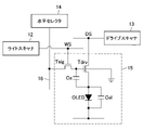
図3に示したように、画素15は、有機EL素子OLEDと、駆動トランジスタTdrvと、映像信号書き込みトランジスタTsigと、保持容量Csと、補助容量Celと、を含んで構成される。
As shown in FIG. 3, the
有機EL素子OLEDは、全ての画素15に対して共通に配線された電源供給線DSにカソード電極が接続されている。そして有機EL素子OLEDを駆動するための駆動回路は、駆動トランジスタTdrvと、映像信号書き込みトランジスタTsigと、保持容量Csと、補助容量Celと、で構成される。
In the organic EL element OLED, the cathode electrode is connected to the power supply line DS which is commonly wired for all the
駆動トランジスタTdrvは、一方の電極(ソース・ドレイン電極)が有機EL素子OLEDのアノード電極に接続され、他方の電極(ソース・ドレイン電極)が電源供給線DSに接続されている。また駆動トランジスタTdrvのバックゲートは接地されている。 In the drive transistor Tdrv, one electrode (source / drain electrode) is connected to the anode electrode of the organic EL element OLED, and the other electrode (source / drain electrode) is connected to the power supply line DS. The back gate of the drive transistor Tdrv is grounded.
映像信号書き込みトランジスタTsigは、一方の電極(ソース・ドレイン電極)が信号線16に接続され、他方の電極(ソース・ドレイン電極)が駆動トランジスタTdrvのゲート電極に接続されている。また、映像信号書き込みトランジスタTsigのゲート電極は、走査線WSに接続されている。
In the video signal writing transistor Tsig, one electrode (source / drain electrode) is connected to the
駆動トランジスタTdrvおよび映像信号書き込みトランジスタTsigにおいて、一方の電極とは、ソース・ドレイン領域に電気的に接続された金属配線をいい、他方の電極とは、ドレイン・ソース領域に電気的に接続された金属配線をいう。また、一方の電極と他方の電極との電位関係によって一方の電極がソース電極ともなればドレイン電極ともなり、他方の電極がドレイン電極ともなればソース電極ともなる。 In the drive transistor Tdrv and the video signal writing transistor Tsig, one electrode is a metal wiring electrically connected to the source / drain region, and the other electrode is electrically connected to the drain / source region. Refers to metal wiring. Further, depending on the potential relationship between one electrode and the other electrode, one electrode may be a source electrode or a drain electrode, and the other electrode may be a drain electrode or a source electrode.
本実施形態では、駆動トランジスタTdrvと、映像信号書き込みトランジスタTsigとで、キャリア移動度が異なるトランジスタを用いる。例えば、映像信号書き込みトランジスタTsigには、シリコン(Si)半導体基板上に形成したMOSトランジスタを用い、駆動トランジスタTdrvには薄膜トランジスタ(Thin Film Transistor;TFT)を用い、それぞれ使い分ける。本実施形態では、映像信号書き込みトランジスタTsigには、例えばnチャネル型のMOSTFTが用いられる。なお、映像信号書き込みトランジスタTsigの導電型はpチャネル型であってもよい。 In this embodiment, a transistor having a different carrier mobility is used between the drive transistor Tdrv and the video signal writing transistor Tsig. For example, a MOS transistor formed on a silicon (Si) semiconductor substrate is used as the video signal writing transistor Tsig, and a thin film transistor (TFT) is used as the drive transistor Tdrv, and these are used properly. In the present embodiment, for example, an n-channel type MOS TFT is used for the video signal writing transistor Tsig. The conductive type of the video signal writing transistor Tsig may be a p-channel type.
Si半導体基板上に形成したMOSトランジスタは、多結晶もしくは非晶質のTFTを用いる場合に比べチャネル移動度が高く、特性バラつきが小さいという特長を有する。本実施形態に係る有機EL表示装置1は、映像信号書き込みトランジスタTsigに、Si半導体基板上に形成したMOSトランジスタを用いることで、この特長から、パネル外部からの映像信号を、その品質を高く維持したまま、駆動トランジスタTdrvのゲート端子に入力することが出来る。 The MOS transistor formed on the Si semiconductor substrate has features that the channel mobility is high and the characteristic variation is small as compared with the case where a polycrystalline or amorphous TFT is used. The organic EL display device 1 according to the present embodiment uses a MOS transistor formed on a Si semiconductor substrate for the video signal writing transistor Tsig, and because of this feature, the video signal from the outside of the panel is maintained at a high quality. It can be input to the gate terminal of the drive transistor Tdrv as it is.
一方、TFTはボディ領域が電気的に浮遊状態のため基板バイアス効果を受けないという特長を有する。従って、本実施形態に係る有機EL表示装置1は、駆動トランジスタにTFTを用いることで、基板バイアス効果による駆動電流の低下、すなわち、表示装置としては輝度の劣化を抑制することができる。さらに、単結晶Si-MOSトランジスタに比べてTFTはチャネル移動度が低いため、図3に示した画素15において、上述したような過剰な移動度補正がかかってしまうことがなく、画面のユニフォーミティが損なわれるようなことも無い。本実施形態では、駆動トランジスタTdrvのキャリア移動度は、映像信号書き込みトランジスタTsigのキャリア移動度より低くなるよう形成される。図3に示した画素15において、駆動トランジスタTdrvのキャリア移動度が映像信号書き込みトランジスタTsigのキャリア移動度より低くなるよう形成されることで、本実施形態に係る有機EL表示装置1は、画面の表示性能の向上が可能となる。
On the other hand, the TFT has a feature that it is not affected by the substrate bias effect because the body region is electrically suspended. Therefore, in the organic EL display device 1 according to the present embodiment, by using the TFT as the drive transistor, it is possible to suppress a decrease in the drive current due to the substrate bias effect, that is, a deterioration in brightness as a display device. Further, since the TFT has a lower channel mobility than the single crystal Si-MOS transistor, the
保持容量Csは、一方の電極(第1ノード)が駆動トランジスタTdrvの他方のソース・ドレイン領域、および、有機EL素子OLEDのアノード電極に接続されており、他方の電極(第2ノード)が駆動トランジスタTdrvのゲート電極および映像信号書き込みトランジスタTsigのソース・ドレイン領域に接続されている。 In the holding capacitance Cs, one electrode (first node) is connected to the other source / drain region of the drive transistor Tdrv and the anode electrode of the organic EL element OLED, and the other electrode (second node) is driven. It is connected to the gate electrode of the transistor Tdrv and the source / drain region of the video signal writing transistor Tsig.
補助容量Celは、一方の電極が有機EL素子OLEDのアノード電極に、他方の電極が電源供給線DSにそれぞれ接続されている。補助容量Celは、有機EL素子OLEDの等価容量の容量不足分を補うべく、その等価容量の補助となって、保持容量Csに対する映像信号の書込みゲインを高めるために設けられている。 In the auxiliary capacitance Cel, one electrode is connected to the anode electrode of the organic EL element OLED, and the other electrode is connected to the power supply line DS. The auxiliary capacity Cel is provided to supplement the equivalent capacity in order to make up for the capacity shortage of the equivalent capacity of the organic EL element OLED, and to increase the write gain of the video signal with respect to the holding capacity Cs.
なお図3においては、補助容量Celの他方の電極が電源供給線DSに接続されるように構成されているが、補助容量Celの他方の電極の接続先としては、電源供給線DSに限られるものではなく、固定電位のノードであればよい。補助容量Celの他方の電極を固定電位のノードに接続することで、有機EL素子OLEDの容量不足分を補い、保持容量Csに対する映像信号の書込みゲインを高めることができる。 In FIG. 3, the other electrode of the auxiliary capacitance Cel is configured to be connected to the power supply line DS, but the connection destination of the other electrode of the auxiliary capacitance Cel is limited to the power supply line DS. It may be a node with a fixed potential, not a node. By connecting the other electrode of the auxiliary capacitance Cel to the node of the fixed potential, it is possible to make up for the capacity shortage of the organic EL element OLED and increase the write gain of the video signal with respect to the holding capacitance Cs.
以上、図3を用いて画素15の具体的な構成例について説明した。続いて、有機EL表示装置1の画素15の動作例について説明する。
As described above, a specific configuration example of the
[1.3.画素の動作例]
図4は、本開示の実施の形態に係る有機EL表示装置1の画素15の動作例をタイミングチャートで示す説明図である。以下、図4を用いて本開示の実施の形態に係る有機EL表示装置1の画素15の動作例について説明する。[1.3. Pixel operation example]
FIG. 4 is an explanatory diagram showing an operation example of the
図4に示したタイミングチャートには、電源供給線DSの電位、走査線WSの電位、信号線16の電位(Vsig/Vofs)、図3の画素15における駆動トランジスタTdrvのゲート電位Gateおよび駆動トランジスタTdrvのソースSourceのそれぞれの変化が示されている。
The timing chart shown in FIG. 4 shows the potential of the power supply line DS, the potential of the scanning line WS, the potential of the signal line 16 (Vsig / Vofs), the gate potential Gate of the drive transistor Tdrv in the
図4において、時刻t0以前は、前の表示フレーム(前フレーム)における有機EL素子OLEDの発光期間となる。前フレームの発光期間では、電源供給線DSの電位が第1電源電位(以下、高電位という)Vccpにあり、また、映像信号書き込みトランジスタTsigが非導通状態にある。 In FIG. 4, before the time t0, it is the light emitting period of the organic EL element OLED in the previous display frame (previous frame). During the light emission period of the previous frame, the potential of the power supply line DS is at the first power supply potential (hereinafter referred to as high potential) Vccp, and the video signal writing transistor Tsig is in a non-conducting state.
ここで、駆動トランジスタTdrvは、飽和領域で動作するように設計されている。これにより、駆動トランジスタTdrvのゲート-ソース間電圧Vgsに応じた駆動電流(ドレイン-ソース間電流)Idsが、電源供給線DSから駆動トランジスタTdrvを通して有機EL素子OLEDに供給される。そして、有機EL素子OLEDは、駆動電流Idsの電流値に応じた輝度で発光する。 Here, the drive transistor Tdrv is designed to operate in the saturation region. As a result, the drive current (drain-source current) Ids corresponding to the gate-source voltage Vgs of the drive transistor Tdrv is supplied from the power supply line DS to the organic EL element OLED through the drive transistor Tdrv. Then, the organic EL element OLED emits light with a brightness corresponding to the current value of the drive current Ids.
時刻t0になると、線順次走査の新しい表示フレーム(現フレーム)に入る。駆動トランジスタTdrvの閾値電圧をVthとすると、電源供給線DSの電位が、高電位Vccpから、信号線16の基準電圧Vofsに対してVofs-Vthよりも十分に低い第2電源電位(以下、低電位という)Viniに切替わる。
At time t0, a new display frame (current frame) for line sequential scanning is entered. Assuming that the threshold voltage of the drive transistor Tdrv is Vth, the potential of the power supply line DS is sufficiently lower than the Vofs-Vth with respect to the reference voltage Vofs of the
ここで、有機EL素子OLEDの閾値電圧をVthel、共通電源供給線の電位(カソード電位)をVcathとする。このとき、低電位Viniを、Vini<Vthel+Vcathとすると、Sourceの電位が低電位Viniに略等しくなるため、有機EL素子OLEDは逆バイアス状態となって消光する。 Here, the threshold voltage of the organic EL element OLED is Vthel, and the potential (cathode potential) of the common power supply line is Vcat. At this time, if the low potential Vini is set to Vini <Vthel + Vcat, the potential of the Source becomes substantially equal to the low potential Vini, so that the organic EL element OLED is in a reverse bias state and extinguished.
続いて、時刻t1において、走査線WSの電位が低電位側から高電位側に遷移することで、映像信号書き込みトランジスタTsigが導通状態となる。このとき、水平セレクタ14から信号線16に対して基準電圧Vofsが供給されている状態にあるため、Gateの電位が基準電圧Vofsになる。また、Sourceの電位は、基準電圧Vofsよりも十分に低い電位、すなわち低電位Viniにある。
Subsequently, at time t1, the potential of the scanning line WS transitions from the low potential side to the high potential side, so that the video signal writing transistor Tsig becomes conductive. At this time, since the reference voltage Vofs is supplied from the
またこのとき、駆動トランジスタTdrvのゲート-ソース間電圧VgsはVofs-Viniとなる。ここで、Vofs-Viniが駆動トランジスタTdrvの閾値電圧Vthよりも大きくないと、後述する閾値補正処理を行うことができないため、Vofs-Vini>Vthとなる関係に設定する必要がある。 At this time, the gate-source voltage Vgs of the drive transistor Tdrv becomes Vofs-Vini. Here, if Vofs-Vini is not larger than the threshold voltage Vth of the drive transistor Tdrv, the threshold correction process described later cannot be performed, so it is necessary to set the relationship of Vofs-Vini> Vth.
このように、Gateの電位を基準電圧Vofsに固定し、かつ、Sourceの電位を低電位Viniに固定して初期化する処理が、後述する閾値補正処理(Vth補正)を行う前の準備(閾値補正準備)の処理である。 In this way, the process of fixing the potential of Gate to the reference voltage Vofs and fixing the potential of Source to the low potential Vini to initialize is the preparation (threshold value) before performing the threshold value correction process (Vth correction) described later. Preparation for correction).
続いて、時刻t2において、電源供給線DSの電位が低電位Viniから高電位Vccpに切替わると、Gateの電位が基準電圧Vofsに保たれた状態で閾値補正処理(Vth補正)が開始される。すなわち、Gateの電位から駆動トランジスタTdrvの閾値電圧Vthを減じた電位に向けてSourceの電位が上昇を開始する。 Subsequently, at time t2, when the potential of the power supply line DS is switched from the low potential Vini to the high potential Vccp, the threshold value correction process (Vth correction) is started while the potential of the Gate is maintained at the reference voltage Vofs. .. That is, the potential of Source starts to rise toward the potential obtained by subtracting the threshold voltage Vth of the drive transistor Tdrv from the potential of Gate.
この閾値補正処理が進むと、やがて駆動トランジスタTdrvのゲート-ソース間電圧Vgsが駆動トランジスタTdrvの閾値電圧Vthに収束する。この閾値電圧Vthに相当する電圧は保持容量Csに保持される。 When this threshold correction process proceeds, the gate-source voltage Vgs of the drive transistor Tdrv eventually converges to the threshold voltage Vth of the drive transistor Tdrv. The voltage corresponding to this threshold voltage Vth is held in the holding capacity Cs.
なお、閾値補正処理を行う期間(閾値補正期間)において、電流が専ら保持容量Cs側に流れ、有機EL素子OLED側には流れないようにするために、有機EL素子OLEDがカットオフ状態となるように、電源供給線には電位Vcathを設定しておくこととする。 In the period for performing the threshold value correction process (threshold value correction period), the organic EL element OLED is in a cutoff state in order to prevent the current from flowing exclusively to the holding capacity Cs side and not to the organic EL element OLED side. As described above, the potential Vcat is set for the power supply line.
続いて時刻t3において、走査線WSの電位が低電位側に遷移することで、映像信号書き込みトランジスタTsigが非導通状態となる。このとき、駆動トランジスタTdrvのゲート電極が信号線16から電気的に切り離されることによってフローティング状態になる。しかしながら、ゲート-ソース間電圧Vgsが駆動トランジスタTdrvの閾値電圧Vthに等しいために、駆動トランジスタTdrvはカットオフ状態にある。したがって、駆動トランジスタTdrvに駆動電流Idsは流れない。
Subsequently, at time t3, the potential of the scanning line WS transitions to the low potential side, so that the video signal writing transistor Tsig is in a non-conducting state. At this time, the gate electrode of the drive transistor Tdrv is electrically disconnected from the
続いて時刻t4において、信号線16の電位が基準電圧Vofsから映像信号の信号電圧Vsigに切替わる。続いて、時刻t5において、走査線WSの電位が高電位側に遷移することで、映像信号書き込みトランジスタTsigは、導通状態となって映像信号の信号電圧Vsigをサンプリングし、映像信号を画素15に書込む。
Subsequently, at time t4, the potential of the
この映像信号書き込みトランジスタTsigによる信号電圧Vsigの書込みにより、Gateの電位が信号電圧Vsigになる。そして、映像信号の信号電圧Vsigによる駆動トランジスタTdrvの駆動の際に、駆動トランジスタTdrvの閾値電圧Vthが、保持容量Csに保持された閾値電圧Vthに相当する電圧と相殺される。 By writing the signal voltage Vsig by the video signal writing transistor Tsig, the potential of Gate becomes the signal voltage Vsig. Then, when the drive transistor Tdrv is driven by the signal voltage Vsig of the video signal, the threshold voltage Vth of the drive transistor Tdrv is offset by the voltage corresponding to the threshold voltage Vth held in the holding capacitance Cs.
このとき、有機EL素子OLEDは、カットオフ状態(ハイインピーダンス状態)にある。従って、映像信号の信号電圧Vsigに応じて電源供給線DSから駆動トランジスタTdrvに流れる駆動電流Idsは、有機EL素子OLEDの等価容量および補助容量Celに流れ込む。これにより、有機EL素子OLEDの等価容量および補助容量Celの充電が開始される。 At this time, the organic EL element OLED is in a cutoff state (high impedance state). Therefore, the drive current Ids flowing from the power supply line DS to the drive transistor Tdrv according to the signal voltage Vsig of the video signal flows into the equivalent capacitance and the auxiliary capacitance Cel of the organic EL element OLED. As a result, charging of the equivalent capacity and auxiliary capacity Cel of the organic EL element OLED is started.
有機EL素子OLEDの等価容量および補助容量Celが充電されることにより、Sourceの電位が時間の経過とともに上昇していく。このとき、すでに、駆動トランジスタTdrvの閾値電圧Vthの画素毎のばらつきがキャンセルされており、駆動トランジスタTdrvの駆動電流Idsは、駆動トランジスタTdrvの移動度μに依存したものとなる。なお、駆動トランジスタTdrvの移動度μは、駆動トランジスタTdrvのチャネルを構成する半導体薄膜の移動度である。 By charging the equivalent capacity and auxiliary capacity Cel of the organic EL element OLED, the potential of Source increases with the passage of time. At this time, the variation in the threshold voltage Vth of the drive transistor Tdrv for each pixel has already been canceled, and the drive current Ids of the drive transistor Tdrv depends on the mobility μ of the drive transistor Tdrv. The mobility μ of the drive transistor Tdrv is the mobility of the semiconductor thin film constituting the channel of the drive transistor Tdrv.
ここで、映像信号の信号電圧Vsigに対する保持容量Csの保持電圧(駆動トランジスタTdrvのゲート-ソース間電圧)Vgsの比率、すなわち書込みゲインが1(理想値)であると仮定する。すると、Sourceの電位がVofs-Vth+ΔVの電位まで上昇することで、駆動トランジスタTdrvのゲート‐ソース間電圧VgsはVsig-Vofs+Vth-ΔVとなる。 Here, it is assumed that the ratio of the holding voltage (gate-source voltage of the drive transistor Tdrv) Vgs to the signal voltage Vsig of the video signal, that is, the write gain is 1 (ideal value). Then, the potential of Source rises to the potential of Vofs-Vth + ΔV, and the gate-source voltage Vgs of the drive transistor Tdrv becomes Vsig-Vth + Vth-ΔV.
すなわち、Sourceの電位の上昇分ΔVは、保持容量Csに保持された電圧(Vsig-Vofs+Vth)から差し引かれるように、すなわち、保持容量Csの充電電荷を放電するように作用する。言い換えると、Sourceの電位の上昇分ΔVは、保持容量Csに対して負帰還がかけられたことになる。従って、Sourceの電位の上昇分ΔVは負帰還の帰還量となる。 That is, the increase ΔV of the potential of the Source acts so as to be subtracted from the voltage (Vsig-Vofs + Vth) held in the holding capacity Cs, that is, to discharge the charge charge of the holding capacity Cs. In other words, the increase in the potential of Source ΔV is negatively fed back to the holding capacity Cs. Therefore, the increase ΔV of the potential of Source is the feedback amount of negative feedback.
このように、駆動トランジスタTdrvに流れる駆動電流Idsに応じた帰還量ΔVでゲート-ソース間電圧Vgsに負帰還をかけることで、駆動トランジスタTdrvの駆動電流Idsの移動度μに対する依存性を打ち消すことができる。この処理が、駆動トランジスタTdrvの移動度μの画素毎のばらつきを補正する移動度補正処理である。 In this way, by applying negative feedback to the gate-source voltage Vgs with the feedback amount ΔV corresponding to the drive current Ids flowing through the drive transistor Tdrv, the dependence of the drive transistor Tdrv on the mobility μ of the drive current Ids can be canceled. Can be done. This process is a mobility correction process that corrects the variation of the mobility μ of the drive transistor Tdrv for each pixel.
続いて、時刻t6において、走査線WSが低電位側に遷移することで、映像信号書き込みトランジスタTsigが非導通状態となる。これにより、駆動トランジスタTdrvのゲート電極は、信号線16から電気的に切り離されるためにフローティング状態になる。
Subsequently, at time t6, the scanning line WS transitions to the low potential side, so that the video signal writing transistor Tsig is in a non-conducting state. As a result, the gate electrode of the drive transistor Tdrv is electrically separated from the
ここで、駆動トランジスタTdrvのゲート電極がフローティング状態にあるときは、駆動トランジスタTdrvのゲート-ソース間に保持容量Csが接続されていることにより、Sourceの電位の変動に連動してGateの電位も変動する。 Here, when the gate electrode of the drive transistor Tdrv is in a floating state, the holding capacitance Cs is connected between the gate and the source of the drive transistor Tdrv, so that the potential of Gate is also linked to the fluctuation of the potential of Source. fluctuate.
このように、駆動トランジスタTdrvのゲート電位がソース電位の変動に連動して変動する動作が、言い換えると、保持容量Csに保持されたゲート-ソース間電圧Vgsを保ったまま、駆動トランジスタTdrvのゲート電位およびソース電位が上昇する動作が、いわゆるブートストラップ動作である。 In this way, the operation in which the gate potential of the drive transistor Tdrv fluctuates in conjunction with the fluctuation of the source potential, in other words, the gate of the drive transistor Tdrv while maintaining the gate-source voltage Vgs held in the holding capacity Cs. The operation in which the potential and the source potential rise is the so-called bootstrap operation.
駆動トランジスタTdrvのゲート電極がフローティング状態になり、それと同時に、駆動トランジスタTdrvの駆動電流Idsが有機EL素子OLEDに流れ始めることにより、有機EL素子OLEDのアノード電位が上昇する。 The gate electrode of the drive transistor Tdrv becomes a floating state, and at the same time, the drive current Ids of the drive transistor Tdrv begins to flow in the organic EL element OLED, so that the anode potential of the organic EL element OLED rises.
そして、有機EL素子OLEDのアノード電位がVthel+Vcathを越えると、有機EL素子OLEDに駆動電流が流れ始め、有機EL素子OLEDが発光を開始する。また、有機EL素子OLEDのアノード電位の上昇は、駆動トランジスタTdrvのソース電位、すなわちSourceの電位の上昇に他ならない。そして、Sourceの電位が上昇すると、保持容量Csのブートストラップ動作により、Gateの電位も連動して上昇する。 Then, when the anode potential of the organic EL element OLED exceeds Vthel + Vcat, a drive current starts to flow in the organic EL element OLED, and the organic EL element OLED starts light emission. Further, the increase in the anode potential of the organic EL element OLED is nothing but an increase in the source potential of the drive transistor Tdrv, that is, the potential of the Source. Then, when the potential of Source rises, the potential of Gate also rises in conjunction with the bootstrap operation of the holding capacity Cs.
このとき、ブートストラップゲインが1(理想値)であると仮定した場合、Gateの電位の上昇量はSourceの電位の上昇量に等しくなる。従って、発光期間中、駆動トランジスタTdrvのゲート-ソース間電圧Vgsは、Vsig-Vofs+Vth-ΔVで一定に保持される。そして、時刻t7で信号線16の電位が映像信号の信号電圧Vsigから基準電圧Vofsに切替わる。
At this time, assuming that the bootstrap gain is 1 (ideal value), the amount of increase in the potential of Gate is equal to the amount of increase in the potential of Source. Therefore, during the light emission period, the gate-source voltage Vgs of the drive transistor Tdrv is kept constant at Vsig-Vofs + Vth-ΔV. Then, at time t7, the potential of the
上述した一連の回路動作において、閾値補正準備、閾値補正、信号電圧Vsigの書込み(信号書込み)、および移動度補正の各処理動作は、1水平走査期間(1H)において実行される。また、信号書込みおよび移動度補正の各処理動作は、時刻t5~t6の期間において並行して実行される。 In the series of circuit operations described above, each processing operation of threshold value correction preparation, threshold value correction, signal voltage Vsig writing (signal writing), and mobility correction is executed in one horizontal scanning period (1H). Further, the signal writing and mobility correction processing operations are executed in parallel during the period from time t5 to t6.
以上、図4を用いて本開示の実施の形態に係る有機EL表示装置1の画素15の動作例について説明した。続いて、本開示の実施の形態に係る有機EL表示装置1の画素15の断面の例を説明する。
As described above, an operation example of the
[1.4.断面例]
本開示の実施の形態に係る有機EL表示装置1の画素15は、上述したように、映像信号書き込みトランジスタTsigには、Si半導体基板上に形成したMOSトランジスタを用い、駆動トランジスタTdrvにはTFTを用い、それぞれ使い分ける。[1.4. Cross section example]
As described above, the
図5は、本開示の実施の形態に係る有機EL表示装置1の画素15に形成される映像信号書き込みトランジスタTsig及び駆動トランジスタTdrvの断面の構成例を示す説明図である。
FIG. 5 is an explanatory diagram showing a configuration example of a cross section of a video signal writing transistor Tsig and a driving transistor Tdrv formed in the
映像信号書き込みトランジスタTsigは、Si基板101にソース・ドレイン領域111、112が形成され、ゲート絶縁膜115上に、ゲート電極114がサイドウォール113に囲まれるよう形成される。
The video signal writing transistor Tsig has source /
一方、駆動トランジスタTdrvは、Si基板101上に形成された酸化膜102の上部にソース・ドレイン領域121、122が形成され、ゲート絶縁膜124上に、ゲート電極125が形成される。
On the other hand, in the drive transistor Tdrv, the source /
このように映像信号書き込みトランジスタTsigにはSi基板101に形成したMOSトランジスタを用い、駆動トランジスタTdrvにはTFTを用いることで、本開示の実施の形態に係る有機EL表示装置1は、映像の高品質化及びユニフォーミティの低下の回避が可能となる。
As described above, by using the MOS transistor formed on the
図6は、本開示の実施の形態に係る有機EL表示装置1の画素15に形成される映像信号書き込みトランジスタTsig及び駆動トランジスタTdrvの断面の別の構成例を示す説明図である。図6に示したのは、SOI(Silicon on Insulator)基板を用いた場合の映像信号書き込みトランジスタTsig及び駆動トランジスタTdrvの断面例である。
FIG. 6 is an explanatory diagram showing another configuration example of a cross section of the video signal writing transistor Tsig and the driving transistor Tdrv formed in the
SOI基板を用いる場合、Si基板101上に埋め込み酸化膜103を形成し、埋め込み酸化膜103の上にソース・ドレイン領域121、122が形成され、ゲート絶縁膜124上に、ゲート電極125が形成されることで駆動トランジスタTdrvが形成される。また埋め込み酸化膜103の上にソース・ドレイン領域111、112が形成され、ゲート絶縁膜115上に、ゲート電極114がサイドウォール113に囲まれるよう形成されることで映像信号書き込みトランジスタTsigが形成される。
When the SOI substrate is used, the embedded
なおSOI基板を用いる場合、映像信号書き込みトランジスタTsigは、動作を安定にするためにボディ領域を接地し、駆動トランジスタTdrvはボディ領域を意図的に浮遊状態にすればよい。駆動トランジスタTdrvのチャネル移動度を下げるには、駆動トランジスタTdrvを形成する領域のみに、選択的に不純物(例えば、アルゴン(Ar)など)をイオン注入してSOI層を非晶質化した後に、図6のように駆動トランジスタTdrvを形成すればよい。また駆動トランジスタTdrvのチャネル移動度を下げるために、駆動トランジスタTdrvを形成する領域のSOI層を選択的に除去した後に駆動トランジスタTdrvとして用いるTFTを形成してもよい When the SOI substrate is used, the video signal writing transistor Tsig may ground the body region in order to stabilize the operation, and the drive transistor Tdrv may intentionally make the body region a floating state. In order to reduce the channel mobility of the drive transistor Tdrv, impurities (for example, argon (Ar)) are selectively ion-implanted only in the region forming the drive transistor Tdrv to amorphize the SOI layer, and then the SOI layer is amorphized. The drive transistor Tdrv may be formed as shown in FIG. Further, in order to reduce the channel mobility of the drive transistor Tdrv, a TFT used as the drive transistor Tdrv may be formed after selectively removing the SOI layer in the region forming the drive transistor Tdrv.
このように、映像信号書き込みトランジスタTsigにはSi基板に形成したMOSトランジスタを用い、駆動トランジスタTdrvにはTFTを用いることで、駆動トランジスタTdrvと駆動トランジスタTdrvとを、ウェル分離を用いて電気的に分離する方法に比べ、駆動トランジスタTdrvの基板バイアス効果の抑制が省スペースで実現できる。 In this way, by using a MOS transistor formed on a Si substrate for the video signal writing transistor Tsig and using a TFT for the drive transistor Tdrv, the drive transistor Tdrv and the drive transistor Tdrv are electrically separated by using well separation. Compared with the separation method, the substrate bias effect of the drive transistor Tdrv can be suppressed in a space-saving manner.
図7は、画素15の断面例を示す説明図であり、映像信号書き込みトランジスタTsig及び駆動トランジスタTdrvを水平方向に並べて形成した場合の例を示す説明図である。
FIG. 7 is an explanatory diagram showing a cross-sectional example of the
図7に示したように映像信号書き込みトランジスタTsig及び駆動トランジスタTdrvを水平方向に並べて形成しても良いが、画素15をより高精細化するために、映像信号書き込みトランジスタTsig及び駆動トランジスタTdrvを積層させて形成してもよい。すなわち、Si基板に映像信号書き込みトランジスタTsigを形成し、映像信号書き込みトランジスタTsigの上部に積層された配線層にTFTとして駆動トランジスタTdrvを形成しても良い。
As shown in FIG. 7, the video signal writing transistor Tsig and the driving transistor Tdrv may be formed side by side in the horizontal direction, but in order to make the
図8は、本開示の実施の形態に係る有機EL表示装置1の画素15の断面例を示す説明図である。図8に示した画素15は、Si基板101上に映像信号書き込みトランジスタTsigを形成し、映像信号書き込みトランジスタTsigの上部に配線層間膜131、132、133を形成し、配線層間膜133が形成された領域に保持容量Cs及び駆動トランジスタTdrvが形成されている。そして図8に示した画素15は、駆動トランジスタTdrvの上部に配線層間膜134、135、136が形成されているとともに、配線層間膜135の上部にアノード電極151、有機材料層152、カソード電極153が形成されている。なおアノード電極151、有機材料層152、カソード電極153によって有機EL素子OLEDが構成される。
FIG. 8 is an explanatory diagram showing a cross-sectional example of the
映像信号書き込みトランジスタTsigの一方のソース・ドレイン領域には、コンタクトホール及びコンタクトビア140を介して映像信号線(Vsig)16が接続され、ゲート電極114にはコンタクトホール及びコンタクトビア140を介して走査線WSが接続される。また、駆動トランジスタTdrvの一方のソース・ドレイン領域121には、コンタクトホール及びコンタクトビア140を介して電源供給線DSが接続されており、ゲート電極125にはコンタクトホール及びコンタクトビア140を介して保持容量Csの一方の電極161が接続されている。保持容量Csの他方の電極162は、有機EL素子OLEDのアノード電極151に接続される。
A video signal line (Vsig) 16 is connected to one source / drain region of the video signal writing transistor Tsig via a contact hole and a contact via 140, and the
Si基板に映像信号書き込みトランジスタTsigを形成し、映像信号書き込みトランジスタTsigの上部に積層された配線層にTFTとして駆動トランジスタTdrvを形成することで、高精細化のために駆動回路を微細化してもトランジスタサイズを小さくしなくて済む。従って、本開示の実施の形態に係る有機EL表示装置は、映像信号書き込みトランジスタTsigと駆動トランジスタTdrvとを図8のように積層させて形成することで、トランジスタ特性のバラつきに起因するユニフォーミティの劣化を回避出来るという効果を有する。 By forming the video signal writing transistor Tsig on the Si substrate and forming the drive transistor Tdrv as a TFT in the wiring layer laminated on the video signal writing transistor Tsig, even if the drive circuit is miniaturized for high definition. There is no need to reduce the transistor size. Therefore, the organic EL display device according to the embodiment of the present disclosure is formed by stacking the video signal writing transistor Tsig and the drive transistor Tdrv as shown in FIG. 8, thereby achieving uniformity due to variation in transistor characteristics. It has the effect of avoiding deterioration.
また、Si基板に映像信号書き込みトランジスタTsigを形成し、映像信号書き込みトランジスタTsigの上部に積層された配線層にTFTとして駆動トランジスタTdrvを形成することで、駆動トランジスタTdrvのゲート長を短くしなくて済むという効果もある。駆動トランジスタTdrvのゲート長が短くなると、ドレイン電圧に依存して駆動トランジスタTdrvの電流が増加するからである。 Further, by forming the video signal writing transistor Tsig on the Si substrate and forming the driving transistor Tdrv as a TFT in the wiring layer laminated on the video signal writing transistor Tsig, the gate length of the driving transistor Tdrv can be shortened. There is also the effect of finishing. This is because when the gate length of the drive transistor Tdrv becomes shorter, the current of the drive transistor Tdrv increases depending on the drain voltage.
図9は、駆動トランジスタTdrvの電圧電流特性の例を示す説明図である。図9に示したグラフの破線は理想的な電圧電流特性の例であり、実線は実際の電圧電流特性の例である。理想的には、駆動トランジスタTdrvのドレイン-ソース間の電圧Vdsがある程度まで低下しても、駆動トランジスタTdrvのドレイン電流Idは不変である。しかし駆動トランジスタTdrvのゲート長が短くなると、実際には、駆動トランジスタTdrvのドレイン-ソース間の電圧Vdsが低下するにつれてドレイン電流Idも低下するために、輝度が劣化する。 FIG. 9 is an explanatory diagram showing an example of the voltage-current characteristics of the drive transistor Tdrv. The broken line in the graph shown in FIG. 9 is an example of an ideal voltage-current characteristic, and the solid line is an example of an actual voltage-current characteristic. Ideally, the drain current Id of the drive transistor Tdrv does not change even if the voltage Vds between the drain and the source of the drive transistor Tdrv drops to some extent. However, when the gate length of the drive transistor Tdrv is shortened, the brightness is actually deteriorated because the drain current Id also decreases as the voltage Vds between the drain and the source of the drive transistor Tdrv decreases.
しかし、駆動トランジスタTdrvのゲート長を長くすることで、駆動トランジスタTdrvの電圧電流特性を理想的な状態に近付けることが出来る。すなわち、駆動トランジスタTdrvのゲート長を長くすることで、電圧Vdsの低下によってもドレイン電流Idが低下せず、輝度の劣化を回避出来る。すなわち、駆動トランジスタTdrvを定電流源に近い状態で使用できることになる。 However, by lengthening the gate length of the drive transistor Tdrv, the voltage-current characteristics of the drive transistor Tdrv can be brought closer to the ideal state. That is, by lengthening the gate length of the drive transistor Tdrv, the drain current Id does not decrease even when the voltage Vds decreases, and the deterioration of the luminance can be avoided. That is, the drive transistor Tdrv can be used in a state close to a constant current source.
また、映像信号書き込みトランジスタTsigと駆動トランジスタTdrvとを並べて形成すると、基板内に形成されるPN接合における寄生容量や寄生リークに起因し、隣接している駆動回路が誤動作を起こし、本来出力したいものとは違う情報が表示される場合がありうる。これに対し、図8のように、映像信号書き込みトランジスタTsigと駆動トランジスタTdrvとを、配線層間膜131、132、133を介して(例えば、500nm以上の酸化膜を介して)遠ざけることで、このような誤動作を回避することが出来る。
Further, when the video signal writing transistor Tsig and the drive transistor Tdrv are formed side by side, the adjacent drive circuit malfunctions due to the parasitic capacitance and the parasitic leak in the PN junction formed in the substrate, and the original output is desired. Information different from that may be displayed. On the other hand, as shown in FIG. 8, the video signal writing transistor Tsig and the driving transistor Tdrv are separated from each other via the
図8に示したのは、保持容量CsをMIMキャパシタとした例であるが、保持容量CsをMIS(Metal Insulator Semiconductor)キャパシタとしてもよい。 FIG. 8 shows an example in which the holding capacity Cs is a MIM capacitor, but the holding capacity Cs may be a MIS (Metal Insulator Semiconductor) capacitor.
図10は、本開示の実施の形態に係る有機EL表示装置1の画素15の別の断面例を示す説明図である。図10に示した画素15は、保持容量CsをMISキャパシタとした例である。保持容量Csを、配線層に形成したMIMキャパシタとする場合に比べ、MISキャパシタは誘電体膜の膜厚を薄くできる。例えば、MISキャパシタは誘電体膜の膜厚を10nm以下の酸化膜とすることが出来る。このため、映像信号書き込みトランジスタTsigのゲート酸化膜厚と、MISキャパシタで構成した保持容量Csの絶縁膜厚とを異ならせることが出来る。従って、保持容量CsをMISキャパシタとすることで、小面積ながらも高い容量を確保することが出来る。
FIG. 10 is an explanatory diagram showing another cross-sectional example of the
なお、図10に示したように映像信号書き込みトランジスタTsigと保持容量Csとを並べて形成する場合、保持容量Csには映像信号書き込みトランジスタTsigと同じ絶縁膜を用いてもよく、保持容量Csの高容量化のために、映像信号書き込みトランジスタTsigと保持容量Csの誘電体膜とを個別に作り分けても良い。 When the video signal writing transistor Tsig and the holding capacity Cs are formed side by side as shown in FIG. 10, the same insulating film as the video signal writing transistor Tsig may be used for the holding capacity Cs, and the holding capacity Cs is high. In order to increase the capacitance, the video signal writing transistor Tsig and the dielectric film having the holding capacitance Cs may be made separately.
<2.まとめ>
以上説明したように本開示の実施の形態によれば、駆動トランジスタと、映像信号書き込みトランジスタとでキャリア移動度が異なるトランジスタ、例えば、映像信号書き込みトランジスタには単結晶Si基板上に形成されたMOSトランジスタを用い、駆動トランジスタにはTFTを用いる、有機EL表示装置1が提供される。<2. Summary>
As described above, according to the embodiment of the present disclosure, a transistor having a different carrier mobility between a drive transistor and a video signal writing transistor, for example, a video signal writing transistor is a MOS formed on a single crystal Si substrate. An organic EL display device 1 using a transistor and a TFT as a drive transistor is provided.
本開示の実施の形態に係る有機EL表示装置1は、駆動トランジスタと、映像信号書き込みトランジスタとでキャリア移動度が異なるトランジスタを用いることで、信号品質を高く維持できるとともに、輝度劣化を起こさず、また移動度補正が過剰にかかることに起因する画面のユニフォーミティが損なわれることを回避出来る。 The organic EL display device 1 according to the embodiment of the present disclosure can maintain high signal quality and does not cause deterioration of brightness by using transistors having different carrier mobilities between the drive transistor and the video signal writing transistor. In addition, it is possible to avoid impairing the uniformity of the screen due to excessive mobility correction.
本開示の実施の形態に係る有機EL表示装置1は、キャリア移動度が異なる駆動トランジスタと、映像信号書き込みトランジスタとを、配線層間膜を介して積層させて形成することができる。駆動トランジスタと、映像信号書き込みトランジスタとを配線層間膜を介して積層させることで、駆動トランジスタのゲート長を長くすることができ、駆動トランジスタTdrvを定電流源に近い状態で使用できる。また駆動トランジスタと、映像信号書き込みトランジスタとを配線層間膜を介して積層させることで、駆動トランジスタと、映像信号書き込みトランジスタとの間のカップリングを抑制し、本来出力したいものとは違う情報が表示される誤動作を回避することが出来る。 The organic EL display device 1 according to the embodiment of the present disclosure can be formed by laminating a drive transistor having different carrier mobility and a video signal writing transistor via a wiring interlayer film. By stacking the drive transistor and the video signal writing transistor via the wiring interlayer film, the gate length of the drive transistor can be lengthened, and the drive transistor Tdrv can be used in a state close to a constant current source. In addition, by stacking the drive transistor and the video signal writing transistor via the wiring interlayer film, the coupling between the drive transistor and the video signal writing transistor is suppressed, and information different from what is originally desired to be output is displayed. It is possible to avoid the malfunction that occurs.
本開示の実施の形態に係る有機EL表示装置1は、様々な機器に搭載することが可能である。例えば、本開示の実施の形態に係る有機EL表示装置1は、テレビジョン受像機、パーソナルコンピュータ、携帯電話、高機能携帯電話(スマートフォン)、タブレット型携帯端末、携帯型音楽プレーヤ、ゲーム機、デジタルスチルカメラ、デジタルビデオカメラ、腕時計型、頭部装着型、ペンダント型その他のウェアラブルコンピュータ等、様々な機器に搭載できる。 The organic EL display device 1 according to the embodiment of the present disclosure can be mounted on various devices. For example, the organic EL display device 1 according to the embodiment of the present disclosure includes a television receiver, a personal computer, a mobile phone, a high-performance mobile phone (smartphone), a tablet-type mobile terminal, a portable music player, a game machine, and a digital device. It can be installed in various devices such as still cameras, digital video cameras, watch-type, head-mounted types, pendant-type and other wearable computers.
以上、添付図面を参照しながら本開示の好適な実施形態について詳細に説明したが、本開示の技術的範囲はかかる例に限定されない。本開示の技術分野における通常の知識を有する者であれば、特許請求の範囲に記載された技術的思想の範疇内において、各種の変更例または修正例に想到し得ることは明らかであり、これらについても、当然に本開示の技術的範囲に属するものと了解される。 Although the preferred embodiments of the present disclosure have been described in detail with reference to the accompanying drawings, the technical scope of the present disclosure is not limited to such examples. It is clear that anyone with ordinary knowledge in the technical field of the present disclosure may come up with various modifications or amendments within the scope of the technical ideas described in the claims. Is, of course, understood to belong to the technical scope of the present disclosure.
例えば、上記実施形態では、発光素子として有機EL素子を用いていたが、本技術はかかる例に限定されない。例えば、無機エレクトロルミネッセンス発光部、LED発光部、半導体レーザー発光部等の自発光型の発光部を用いた表示装置に対しても、上記実施形態と同様に、駆動トランジスタと、映像信号書き込みトランジスタとはキャリア移動度が異なるトランジスタを用いてもよい。 For example, in the above embodiment, the organic EL element is used as the light emitting element, but the present technique is not limited to such an example. For example, for a display device using a self-luminous light emitting unit such as an inorganic electroluminescence light emitting unit, an LED light emitting unit, and a semiconductor laser light emitting unit, a drive transistor and a video signal writing transistor may be used as in the above embodiment. May use transistors having different carrier mobility.
また、本明細書に記載された効果は、あくまで説明的または例示的なものであって限定的ではない。つまり、本開示に係る技術は、上記の効果とともに、または上記の効果に代えて、本明細書の記載から当業者には明らかな他の効果を奏しうる。 In addition, the effects described herein are merely explanatory or exemplary and are not limited. That is, the techniques according to the present disclosure may have other effects apparent to those skilled in the art from the description herein, in addition to or in place of the above effects.
なお、以下のような構成も本開示の技術的範囲に属する。
(1)
発光部及び前記発光部を駆動するための駆動回路を備えた発光素子を複数有し、
前記駆動回路は、
前記発光部を制御する駆動トランジスタと、
映像信号の書き込みを制御する映像信号書き込みトランジスタと、
容量素子と、
を備え、
前記駆動トランジスタは、一方のソース・ドレイン領域が電流供給線に接続され、他方のソース・ドレイン領域が前記発光部及び前記容量素子の第1ノードに接続され、ゲート電極が前記容量素子の第2ノードに接続され、
前記映像信号書き込みトランジスタは、一方のソース・ドレイン領域がデータ線に接続され、他方のソース・ドレイン領域が前記駆動トランジスタのゲート電極及び前記容量素子の第2ノードに接続され、ゲート電極が走査線に接続され、
前記駆動トランジスタと、前記映像信号書き込みトランジスタとはキャリア移動度が異なる、表示装置。
(2)
前記駆動トランジスタのキャリア移動度は、前記映像信号書き込みトランジスタのキャリア移動度より低い、前記(1)に記載の表示装置。
(3)
前記映像信号書き込みトランジスタはシリコン半導体基板上に形成され、前記駆動トランジスタは薄膜トランジスタを用いる、前記(1)に記載の表示装置。
(4)
前記駆動トランジスタは、nチャネル型のMOSトランジスタである、前記(2)に記載の表示装置。
(5)
前記駆動トランジスタは配線層に形成される、前記(2)または(3)に記載の表示装置。
(6)
前記駆動トランジスタと前記映像信号書き込みトランジスタとは水平方向において少なくとも一部が重なる位置に形成される、前記(5)に記載の表示装置。
(7)
前記容量素子は、前記駆動トランジスタのソース・ドレイン領域を第1ノードとして、前記映像信号書き込みトランジスタのソース・ドレイン領域を第2ノードとする、前記(1)~(6)のいずれかに記載の表示装置。
(8)
前記容量素子は、MIS(Metal Insulator Semiconductor)キャパシタである前記(7)に記載の表示装置。
(9)
前記映像信号書き込みトランジスタのゲート酸化膜厚と、前記MISキャパシタの絶縁膜厚とが異なる、前記(8)に記載の表示装置。
(10)
前記(1)~(9)のいずれかに記載の表示装置を備える、電子機器。The following configurations also belong to the technical scope of the present disclosure.
(1)
It has a plurality of light emitting elements having a light emitting unit and a drive circuit for driving the light emitting unit, and has a plurality of light emitting elements.
The drive circuit
The drive transistor that controls the light emitting part and
A video signal writing transistor that controls the writing of video signals,
Capacitive element and
Equipped with
In the drive transistor, one source / drain region is connected to the current supply line, the other source / drain region is connected to the light emitting portion and the first node of the capacitive element, and the gate electrode is the second of the capacitive element. Connected to the node
In the video signal writing transistor, one source / drain region is connected to a data line, the other source / drain region is connected to the gate electrode of the drive transistor and the second node of the capacitive element, and the gate electrode is a scanning line. Connected to
A display device in which the carrier mobility differs between the drive transistor and the video signal writing transistor.
(2)
The display device according to (1), wherein the carrier mobility of the drive transistor is lower than the carrier mobility of the video signal writing transistor.
(3)
The display device according to (1) above, wherein the video signal writing transistor is formed on a silicon semiconductor substrate, and the driving transistor uses a thin film transistor.
(4)
The display device according to (2) above, wherein the drive transistor is an n-channel type MOS transistor.
(5)
The display device according to (2) or (3) above, wherein the drive transistor is formed in a wiring layer.
(6)
The display device according to (5) above, wherein the drive transistor and the video signal writing transistor are formed at a position where at least a part of the drive transistor and the video signal writing transistor overlap each other in the horizontal direction.
(7)
The capacitive element according to any one of (1) to (6) above, wherein the source / drain region of the drive transistor is the first node and the source / drain region of the video signal writing transistor is the second node. Display device.
(8)
The display device according to (7) above, wherein the capacitive element is a MIS (Metal Insulator Semiconductor) capacitor.
(9)
The display device according to (8), wherein the gate oxide film thickness of the video signal writing transistor and the insulation film thickness of the MIS capacitor are different.
(10)
An electronic device including the display device according to any one of (1) to (9).
1 :有機EL表示装置
11 :画素アレイ部
12 :ライトスキャナ
13 :ドライブスキャナ
14 :水平セレクタ
15 :画素
16 :信号線
32 :電源供給線
101 :Si基板
102 :酸化膜
103 :埋め込み酸化膜
111 :ソース・ドレイン領域
112 :ソース・ドレイン領域
113 :サイドウォール
114 :ゲート電極
115 :ゲート絶縁膜
121 :ソース・ドレイン領域
122 :ソース・ドレイン領域
124 :ゲート絶縁膜
125 :ゲート電極
131 :配線層間膜
132 :配線層間膜
133 :配線層間膜
134 :配線層間膜
135 :配線層間膜
136 :配線層間膜
140 :コンタクトホール及びコンタクトビア
151 :アノード電極
152 :有機材料層
153 :カソード電極
161 :電極
162 :電極
Cs :保持容量
Cel :補助容量
DS :電源供給線
Tdrv :駆動トランジスタ
Tsig :映像信号書き込みトランジスタ
WS :走査線1: Organic EL display device 11: Pixel array unit 12: Light scanner 13: Drive scanner 14: Horizontal selector 15: Pixel 16: Signal line 32: Power supply line 101: Si substrate 102: Oxidation film 103: Embedded oxide film 111: Source / drain region 112: Source / drain region 113: Sidewall 114: Gate electrode 115: Gate insulating film 121: Source / drain region 122: Source / drain region 124: Gate insulating film 125: Gate electrode 131: Wiring interlayer film 132 : Wiring interlayer film 133: Wiring interlayer film 134: Wiring interlayer film 135: Wiring interlayer film 136: Wiring interlayer film 140: Contact hole and contact via 151: Anode electrode 152: Organic material layer 153: Cathode electrode 161: Electrode 162: Electrode Cs: Holding capacity Cel: Auxiliary capacity DS: Power supply line Tdrv: Drive transistor Tsig: Video signal writing transistor WS: Scanning line
Claims (9)
前記駆動回路は、
前記発光部を制御する駆動トランジスタと、
シリコン半導体基板に形成されたMOSトランジスタにより構成されて映像信号の書き込みを制御する映像信号書き込みトランジスタと、
容量素子と、
を備え、
前記駆動トランジスタは、前記シリコン半導体基板に積層された配線層間膜に形成される薄膜トランジスタにより構成されて、一方のソース・ドレイン領域が電流供給線に接続され、他方のソース・ドレイン領域が前記発光部及び前記容量素子の第1ノードに接続され、ゲート電極が前記容量素子の第2ノードに接続され、
前記映像信号書き込みトランジスタは、一方のソース・ドレイン領域がデータ線に接続され、他方のソース・ドレイン領域が前記駆動トランジスタのゲート電極及び前記容量素子の第2ノードに接続され、ゲート電極が走査線に接続され、
前記駆動トランジスタは、前記映像信号書き込みトランジスタ及び前記容量素子とは異なる層に配置されるとともに前記シリコン半導体基板表面に対する法線方向から見て少なくとも一部が重なる位置に形成され、
前記駆動トランジスタのキャリア移動度は、前記映像信号書き込みトランジスタのキャリア移動度より低い、表示装置。 It has a plurality of light emitting elements having a light emitting unit and a drive circuit for driving the light emitting unit, and has a plurality of light emitting elements.
The drive circuit
The drive transistor that controls the light emitting part and
A video signal writing transistor that is composed of MOS transistors formed on a silicon semiconductor substrate and controls the writing of video signals.
Capacitive element and
Equipped with
The drive transistor is composed of a thin film transistor formed on a wiring interlayer film laminated on the silicon semiconductor substrate, one source / drain region is connected to a current supply line, and the other source / drain region is the light emitting unit. And connected to the first node of the capacitive element, the gate electrode is connected to the second node of the capacitive element,
In the video signal writing transistor, one source / drain region is connected to a data line, the other source / drain region is connected to the gate electrode of the drive transistor and the second node of the capacitive element, and the gate electrode is a scanning line. Connected to
The drive transistor is arranged in a layer different from the video signal writing transistor and the capacitive element, and is formed at a position where at least a part of the drive transistor overlaps with respect to the surface of the silicon semiconductor substrate when viewed from the normal direction .
A display device in which the carrier mobility of the drive transistor is lower than the carrier mobility of the video signal writing transistor.
Applications Claiming Priority (3)
| Application Number | Priority Date | Filing Date | Title |
|---|---|---|---|
| JP2016085682 | 2016-04-22 | ||
| JP2016085682 | 2016-04-22 | ||
| PCT/JP2017/009691 WO2017183355A1 (en) | 2016-04-22 | 2017-03-10 | Display apparatus and electronic device |
Publications (2)
| Publication Number | Publication Date |
|---|---|
| JPWO2017183355A1 JPWO2017183355A1 (en) | 2019-02-28 |
| JP7100577B2 true JP7100577B2 (en) | 2022-07-13 |
Family
ID=60116021
Family Applications (1)
| Application Number | Title | Priority Date | Filing Date |
|---|---|---|---|
| JP2018513064A Active JP7100577B2 (en) | 2016-04-22 | 2017-03-10 | Display devices and electronic devices |
Country Status (5)
| Country | Link |
|---|---|
| US (3) | US11081057B2 (en) |
| JP (1) | JP7100577B2 (en) |
| CN (3) | CN113936601A (en) |
| DE (1) | DE112017002103B4 (en) |
| WO (1) | WO2017183355A1 (en) |
Families Citing this family (9)
| Publication number | Priority date | Publication date | Assignee | Title |
|---|---|---|---|---|
| JP6867737B2 (en) * | 2016-08-30 | 2021-05-12 | ソニーセミコンダクタソリューションズ株式会社 | Display devices and electronic devices |
| JP7011449B2 (en) * | 2017-11-21 | 2022-01-26 | ソニーセミコンダクタソリューションズ株式会社 | Pixel circuits, display devices and electronic devices |
| EP3861715A4 (en) * | 2018-10-27 | 2022-04-27 | Huawei Technologies Co., Ltd. | Sensor and display device |
| WO2021064954A1 (en) * | 2019-10-03 | 2021-04-08 | シャープ株式会社 | Display device |
| KR20210116735A (en) * | 2020-03-12 | 2021-09-28 | 삼성디스플레이 주식회사 | Display device and driving method thereof |
| TWI744024B (en) * | 2020-10-07 | 2021-10-21 | 聯嘉光電股份有限公司 | Crystal grain structure of miniature light-emitting diode display |
| CN113013163A (en) * | 2021-02-25 | 2021-06-22 | 安徽熙泰智能科技有限公司 | Micro-display driving chip structure and manufacturing process thereof |
| CN112951824A (en) * | 2021-02-25 | 2021-06-11 | 安徽熙泰智能科技有限公司 | Combined driving chip structure for micro-display and manufacturing process thereof |
| CN114005409B (en) * | 2021-10-29 | 2022-11-25 | 绵阳惠科光电科技有限公司 | Pixel driving circuit, method and display panel |
Citations (3)
| Publication number | Priority date | Publication date | Assignee | Title |
|---|---|---|---|---|
| JP2005300786A (en) | 2004-04-09 | 2005-10-27 | Sanyo Electric Co Ltd | Display device and method for manufacturing the same |
| JP2015194577A (en) | 2014-03-31 | 2015-11-05 | ソニー株式会社 | Display device and electronic apparatus |
| US20160064421A1 (en) | 2014-08-29 | 2016-03-03 | Lg Display Co., Ltd. | Thin film transistor substrate and display device using the same |
Family Cites Families (40)
| Publication number | Priority date | Publication date | Assignee | Title |
|---|---|---|---|---|
| TW486869B (en) * | 1999-12-27 | 2002-05-11 | Sanyo Electric Co | Voltage producing circuit and a display device provided with such voltage producing circuit |
| US20030003665A1 (en) * | 2001-06-27 | 2003-01-02 | Nakagawa Osamu Samuel | Process for high-dielectric constant metal-insulator metal capacitor in VLSI multi-level metallization systems |
| JP3800050B2 (en) * | 2001-08-09 | 2006-07-19 | 日本電気株式会社 | Display device drive circuit |
| KR100458710B1 (en) * | 2001-11-06 | 2004-12-03 | 네오폴리((주)) | A Crystalline Silicon Thin Film Transistor Panel for OELD and a Fabrication Method Thereof |
| US7230592B2 (en) * | 2002-03-04 | 2007-06-12 | Hitachi, Ltd. | Organic electroluminescent light emitting display device |
| JP4683825B2 (en) | 2002-04-24 | 2011-05-18 | 株式会社半導体エネルギー研究所 | Semiconductor device and manufacturing method thereof |
| JP4128045B2 (en) * | 2002-07-26 | 2008-07-30 | 三洋電機株式会社 | Organic EL panel |
| KR100466628B1 (en) * | 2002-11-12 | 2005-01-15 | 삼성에스디아이 주식회사 | Flat panel display and fabrication method thereof |
| TWI334313B (en) * | 2005-02-23 | 2010-12-01 | Au Optronics Corp | Organic electroluminiscent display and fabricating method thereof |
| JP2006284915A (en) * | 2005-03-31 | 2006-10-19 | Toshiba Matsushita Display Technology Co Ltd | Display device and array substrate |
| TWI429327B (en) * | 2005-06-30 | 2014-03-01 | Semiconductor Energy Lab | Semiconductor device, display device, and electronic appliance |
| JP2007316510A (en) * | 2006-05-29 | 2007-12-06 | Toshiba Matsushita Display Technology Co Ltd | Active matrix type display device |
| JP2008085091A (en) * | 2006-09-28 | 2008-04-10 | Sony Corp | Method for manufacturing thin film transistor, thin film transistor, and display unit |
| JP2008256916A (en) * | 2007-04-04 | 2008-10-23 | Sony Corp | Driving method of organic electroluminescence light emission part |
| JP4479755B2 (en) * | 2007-07-03 | 2010-06-09 | ソニー株式会社 | ORGANIC ELECTROLUMINESCENT ELEMENT AND ORGANIC ELECTROLUMINESCENT DISPLAY DEVICE |
| JP5251034B2 (en) * | 2007-08-15 | 2013-07-31 | ソニー株式会社 | Display device and electronic device |
| JP4978435B2 (en) * | 2007-11-14 | 2012-07-18 | ソニー株式会社 | Display device, display device driving method, and electronic apparatus |
| JP5181164B2 (en) * | 2008-03-17 | 2013-04-10 | ユー・ディー・シー アイルランド リミテッド | Organic electroluminescence display |
| JP2009271200A (en) * | 2008-05-01 | 2009-11-19 | Sony Corp | Display apparatus and driving method for display apparatus |
| KR101341011B1 (en) * | 2008-05-17 | 2013-12-13 | 엘지디스플레이 주식회사 | Light emitting display |
| KR101681884B1 (en) * | 2009-03-27 | 2016-12-05 | 가부시키가이샤 한도오따이 에네루기 켄큐쇼 | Semiconductor device, display device, and electronic appliance |
| KR101022652B1 (en) * | 2009-04-02 | 2011-03-22 | 삼성모바일디스플레이주식회사 | Method for manufacturing thin film transistor substrate and method for manufacturing organic light emitting display apparatus |
| JP2010243938A (en) * | 2009-04-09 | 2010-10-28 | Sony Corp | Display and method of driving the same |
| JP5644511B2 (en) * | 2011-01-06 | 2014-12-24 | ソニー株式会社 | Organic EL display device and electronic device |
| JP2012255874A (en) | 2011-06-08 | 2012-12-27 | Sony Corp | Pixel circuit, display device, electronic appliance, and driving method for pixel circuit |
| JP5870546B2 (en) * | 2011-08-23 | 2016-03-01 | ソニー株式会社 | Display device and electronic device |
| KR20130024029A (en) * | 2011-08-30 | 2013-03-08 | 삼성디스플레이 주식회사 | Organic light emitting diode display and method for manufacturing the same |
| CN103189970B (en) * | 2011-10-28 | 2016-09-28 | 株式会社日本有机雷特显示器 | Thin film semiconductor device and the manufacture method of thin film semiconductor device |
| TW201324760A (en) * | 2011-12-07 | 2013-06-16 | Chunghwa Picture Tubes Ltd | Pixel structure and manufacturing method of the same |
| JP2013168341A (en) * | 2012-02-17 | 2013-08-29 | Seiko Epson Corp | Organic el device and electronic apparatus |
| JP6056175B2 (en) * | 2012-04-03 | 2017-01-11 | セイコーエプソン株式会社 | Electro-optical device and electronic apparatus |
| JP6031652B2 (en) * | 2012-08-31 | 2016-11-24 | 株式会社Joled | Display device and electronic device |
| JP6286941B2 (en) * | 2013-08-27 | 2018-03-07 | セイコーエプソン株式会社 | LIGHT EMITTING DEVICE, LIGHT EMITTING DEVICE MANUFACTURING METHOD, ELECTRONIC DEVICE |
| JP5770236B2 (en) * | 2013-09-18 | 2015-08-26 | 株式会社ジャパンディスプレイ | Display device |
| US9083320B2 (en) * | 2013-09-20 | 2015-07-14 | Maofeng YANG | Apparatus and method for electrical stability compensation |
| TWI663726B (en) * | 2014-05-30 | 2019-06-21 | Semiconductor Energy Laboratory Co., Ltd. | Semiconductor device, module, and electronic device |
| KR102296945B1 (en) * | 2014-07-04 | 2021-09-01 | 엘지디스플레이 주식회사 | Organic light emitting display and method of fabricating the same |
| EP2966705B1 (en) * | 2014-07-11 | 2018-09-19 | LG Display Co., Ltd. | Organic light-emitting diode display device and method of fabricating the same |
| CN104201188B (en) * | 2014-08-22 | 2017-07-25 | 京东方科技集团股份有限公司 | OLED pixel unit and preparation method thereof, display panel and display device |
| KR20180099020A (en) * | 2017-02-28 | 2018-09-05 | 엘지디스플레이 주식회사 | Electroluminescent Display Device |
-
2017
- 2017-03-10 CN CN202111209606.2A patent/CN113936601A/en active Pending
- 2017-03-10 US US16/088,162 patent/US11081057B2/en active Active
- 2017-03-10 JP JP2018513064A patent/JP7100577B2/en active Active
- 2017-03-10 WO PCT/JP2017/009691 patent/WO2017183355A1/en active Application Filing
- 2017-03-10 DE DE112017002103.0T patent/DE112017002103B4/en active Active
- 2017-03-10 CN CN202111209345.4A patent/CN113948560A/en active Pending
- 2017-03-10 CN CN201780023790.7A patent/CN109074765B/en active Active
-
2021
- 2021-07-20 US US17/380,346 patent/US11710456B2/en active Active
-
2023
- 2023-06-20 US US18/337,754 patent/US20240038178A1/en active Pending
Patent Citations (3)
| Publication number | Priority date | Publication date | Assignee | Title |
|---|---|---|---|---|
| JP2005300786A (en) | 2004-04-09 | 2005-10-27 | Sanyo Electric Co Ltd | Display device and method for manufacturing the same |
| JP2015194577A (en) | 2014-03-31 | 2015-11-05 | ソニー株式会社 | Display device and electronic apparatus |
| US20160064421A1 (en) | 2014-08-29 | 2016-03-03 | Lg Display Co., Ltd. | Thin film transistor substrate and display device using the same |
Also Published As
| Publication number | Publication date |
|---|---|
| DE112017002103B4 (en) | 2022-06-15 |
| US11081057B2 (en) | 2021-08-03 |
| JPWO2017183355A1 (en) | 2019-02-28 |
| CN113948560A (en) | 2022-01-18 |
| US11710456B2 (en) | 2023-07-25 |
| US20240038178A1 (en) | 2024-02-01 |
| DE112017002103T5 (en) | 2019-01-03 |
| CN109074765B (en) | 2021-11-05 |
| US20220028343A1 (en) | 2022-01-27 |
| CN113936601A (en) | 2022-01-14 |
| CN109074765A (en) | 2018-12-21 |
| WO2017183355A1 (en) | 2017-10-26 |
| US20200302873A1 (en) | 2020-09-24 |
Similar Documents
| Publication | Publication Date | Title |
|---|---|---|
| JP7100577B2 (en) | Display devices and electronic devices | |
| US10885837B2 (en) | Driving circuit for a light-emitting unit of a display device and electronic apparatus | |
| TWI729671B (en) | Electronic display with hybrid in-pixel and external compensation | |
| US10559256B2 (en) | Pixel driver circuitry for a display device | |
| US9792860B2 (en) | Light-emitting element, display device and electronic apparatus | |
| WO2020001026A1 (en) | Pixel driving circuit and method, and display panel | |
| US10546526B2 (en) | Display device | |
| TWI633529B (en) | Display, display drive circuit, display drive method, and electronic apparatus | |
| JP2014160203A (en) | Display unit and driving method of the same, and electronic apparatus | |
| US20240029652A1 (en) | Pixel circuit, display device, and electronic apparatus | |
| JP2010139926A (en) | Electronic equipment and display device | |
| JP2004341351A (en) | Active matrix type display device | |
| US10985216B2 (en) | Display apparatus and imaging apparatus | |
| JP2009282191A (en) | Display device, method for driving display device, and electronic equipment | |
| JP2014163972A (en) | Display device, method of driving the same, and electronic apparatus | |
| JP2010276734A (en) | Display device, method for driving the display device and electronic equipment |
Legal Events
| Date | Code | Title | Description |
|---|---|---|---|
| RD04 | Notification of resignation of power of attorney |
Free format text: JAPANESE INTERMEDIATE CODE: A7424 Effective date: 20190208 |
|
| RD03 | Notification of appointment of power of attorney |
Free format text: JAPANESE INTERMEDIATE CODE: A7423 Effective date: 20190214 |
|
| RD04 | Notification of resignation of power of attorney |
Free format text: JAPANESE INTERMEDIATE CODE: A7424 Effective date: 20190222 |
|
| RD02 | Notification of acceptance of power of attorney |
Free format text: JAPANESE INTERMEDIATE CODE: A7422 Effective date: 20190515 |
|
| RD04 | Notification of resignation of power of attorney |
Free format text: JAPANESE INTERMEDIATE CODE: A7424 Effective date: 20190522 |
|
| A621 | Written request for application examination |
Free format text: JAPANESE INTERMEDIATE CODE: A621 Effective date: 20200302 |
|
| A131 | Notification of reasons for refusal |
Free format text: JAPANESE INTERMEDIATE CODE: A131 Effective date: 20200915 |
|
| A521 | Request for written amendment filed |
Free format text: JAPANESE INTERMEDIATE CODE: A523 Effective date: 20201027 |
|
| A02 | Decision of refusal |
Free format text: JAPANESE INTERMEDIATE CODE: A02 Effective date: 20210202 |
|
| A521 | Request for written amendment filed |
Free format text: JAPANESE INTERMEDIATE CODE: A523 Effective date: 20210506 |
|
| C60 | Trial request (containing other claim documents, opposition documents) |
Free format text: JAPANESE INTERMEDIATE CODE: C60 Effective date: 20210506 |
|
| A911 | Transfer to examiner for re-examination before appeal (zenchi) |
Free format text: JAPANESE INTERMEDIATE CODE: A911 Effective date: 20210513 |
|
| C21 | Notice of transfer of a case for reconsideration by examiners before appeal proceedings |
Free format text: JAPANESE INTERMEDIATE CODE: C21 Effective date: 20210518 |
|
| A912 | Re-examination (zenchi) completed and case transferred to appeal board |
Free format text: JAPANESE INTERMEDIATE CODE: A912 Effective date: 20210604 |
|
| C211 | Notice of termination of reconsideration by examiners before appeal proceedings |
Free format text: JAPANESE INTERMEDIATE CODE: C211 Effective date: 20210608 |
|
| C22 | Notice of designation (change) of administrative judge |
Free format text: JAPANESE INTERMEDIATE CODE: C22 Effective date: 20211019 |
|
| C13 | Notice of reasons for refusal |
Free format text: JAPANESE INTERMEDIATE CODE: C13 Effective date: 20220201 |
|
| C19 | Decision taken to dismiss amendment |
Free format text: JAPANESE INTERMEDIATE CODE: C19 Effective date: 20220215 |
|
| C30A | Notification sent |
Free format text: JAPANESE INTERMEDIATE CODE: C3012 Effective date: 20220215 |
|
| A521 | Request for written amendment filed |
Free format text: JAPANESE INTERMEDIATE CODE: A523 Effective date: 20220404 |
|
| C22 | Notice of designation (change) of administrative judge |
Free format text: JAPANESE INTERMEDIATE CODE: C22 Effective date: 20220426 |
|
| C23 | Notice of termination of proceedings |
Free format text: JAPANESE INTERMEDIATE CODE: C23 Effective date: 20220510 |
|
| C03 | Trial/appeal decision taken |
Free format text: JAPANESE INTERMEDIATE CODE: C03 Effective date: 20220607 |
|
| C30A | Notification sent |
Free format text: JAPANESE INTERMEDIATE CODE: C3012 Effective date: 20220607 |
|
| A61 | First payment of annual fees (during grant procedure) |
Free format text: JAPANESE INTERMEDIATE CODE: A61 Effective date: 20220701 |
|
| R150 | Certificate of patent or registration of utility model |
Ref document number: 7100577 Country of ref document: JP Free format text: JAPANESE INTERMEDIATE CODE: R150 |