JP7098413B2 - Imaging device - Google Patents
Imaging device Download PDFInfo
- Publication number
- JP7098413B2 JP7098413B2 JP2018095427A JP2018095427A JP7098413B2 JP 7098413 B2 JP7098413 B2 JP 7098413B2 JP 2018095427 A JP2018095427 A JP 2018095427A JP 2018095427 A JP2018095427 A JP 2018095427A JP 7098413 B2 JP7098413 B2 JP 7098413B2
- Authority
- JP
- Japan
- Prior art keywords
- wiring
- flexible printed
- connection
- board
- wiring portion
- Prior art date
- Legal status (The legal status is an assumption and is not a legal conclusion. Google has not performed a legal analysis and makes no representation as to the accuracy of the status listed.)
- Active
Links
Images


Landscapes
- Adjustment Of Camera Lenses (AREA)
- Camera Bodies And Camera Details Or Accessories (AREA)
Description
本発明は、撮像装置に関し、特に、撮像素子を含むユニットを変位させて光学的に像ブレを補正する補正手段を有する撮像装置に関する。 The present invention relates to an image pickup device, and more particularly to an image pickup device having a correction means for displacing a unit including an image pickup element to optically correct image blur.
近年、撮像装置において、撮像素子を含むユニットを変位させて光学的に被写体のブレを補正する補正手段の搭載が進んでいる。このような補正手段では、主として撮像素子を含む可動ユニットを光軸と直交方向に変位させることで被写体のブレ補正を行っている。可動ユニットには、撮像素子を実装した回路基板が搭載され、この回路基板には、コネクタ等の電気的接続部品も実装されている。可動ユニットを保持する固定筐体側には、可動ユニットの駆動制御を行う制御基板が搭載され、この制御基板には、コネクタ等の電気的接続部品も実装されている。可動ユニット側のコネクタと固定筐体側のコネクタとは、フレキシブルプリント基板によって電気的に接続されている。このフレキシブルプリント基板の持つ可撓性を利用して、固定筐体は可動ユニットを電気的に接続しつつ、可動ユニットを駆動制御している(特許文献1)。 In recent years, in an image pickup apparatus, a correction means for optically correcting a blur of a subject by displacing a unit including an image pickup element has been installed. In such a correction means, the blur correction of the subject is mainly performed by displacing the movable unit including the image pickup element in the direction orthogonal to the optical axis. A circuit board on which an image sensor is mounted is mounted on the movable unit, and electrical connection components such as connectors are also mounted on the circuit board. A control board that controls the drive of the movable unit is mounted on the fixed housing side that holds the movable unit, and electrical connection parts such as connectors are also mounted on the control board. The connector on the movable unit side and the connector on the fixed housing side are electrically connected by a flexible printed circuit board. Utilizing the flexibility of this flexible printed circuit board, the fixed housing electrically connects the movable unit and drives and controls the movable unit (Patent Document 1).
可動ユニットと固定筐体とを電気的に接続しているフレキシブルプリント基板は、可動ユニットの変位に応じて配線部の一部が変形することが可能になっている。フレキシブルプリント基板の変形によって生じる反力は、可動ユニットを駆動する際の負荷になる。そのため、負荷低減を図る方法の一例として、フレキシブルプリント基板の可撓部分の長さを長く形成してフレキシブルプリント基板の単位長さあたりの変形量を小さくし、フレキシブルプリント基板の変形によって生じる反力を小さくする方法が考えられる。しかし、このような対策では、フレキシブルプリント基板を収容する空間が大きくなってしまい、撮像装置が大型化してしまう恐れがある。 In the flexible printed board that electrically connects the movable unit and the fixed housing, a part of the wiring portion can be deformed according to the displacement of the movable unit. The reaction force generated by the deformation of the flexible printed circuit board becomes a load when driving the movable unit. Therefore, as an example of a method for reducing the load, the length of the flexible portion of the flexible printed circuit board is formed to be long to reduce the amount of deformation per unit length of the flexible printed circuit board, and the reaction force generated by the deformation of the flexible printed circuit board is reduced. Is conceivable. However, with such measures, the space for accommodating the flexible printed circuit board becomes large, and the image pickup apparatus may become large in size.
本発明は、上記課題を鑑みて、フレキシブルプリント基板の変形によって生じる負荷の増大を抑えつつ、小型化できる撮像装置を提供することを目的とする。 In view of the above problems, it is an object of the present invention to provide an image pickup apparatus that can be miniaturized while suppressing an increase in load caused by deformation of a flexible printed circuit board.
上記の課題を解決するために、本発明の撮像装置は、筐体と、前記筐体に対して光軸と直交する方向に移動可能な可動ユニットを有する撮像装置であって、前記可動ユニットに固定され、撮像素子を実装する基板と、前記基板と電気的に接続されるフレキシブルプリント基板と、前記筐体に固定され、光軸と直交する平面に対して前記基板と平行に配置されて前記フレキシブルプリント基板を介して前記基板と電気的に接続される制御基板と、を備え、前記フレキシブルプリント基板は、前記基板と接続するための第一の接続部と、可撓性を有し、前記第一の接続部を中心として対称な方向に延在し、前記第一の接続部から等しい長さ及びほぼ等しい幅を有する第一の配線部及び第二の配線部と、前記第一の配線部の端部に設けられ、前記制御基板と接続されるための第二の接続部と、前記第二の配線部の端部に設けられ、前記制御基板と接続されるための第三の接続部とを備え、前記撮像素子の有効画素中心が前記光軸の中心と一致する姿勢において、前記第一の配線部及び前記第二の配線部を湾曲させて、前記第二の接続部及び前記第三の接続部を前記制御基板と電気的に接続した状態で、前記第一の接続部と前記第一の配線部との境界から前記第二の接続部と前記第一の配線部との境界までの距離が、前記第一の接続部と前記第二の配線部との境界から前記第三の接続部と前記第二の配線部との境界までの距離と、同じ距離に形成し、前記フレキシブルプリント基板は、前記撮像素子と前記制御基板を電気的に接続する複数の差動信号配線パターンをさらに備え、前記複数の差動信号配線パターンは、前記第一の配線部に配線される第一の差動信号配線パターンと、前記第二の配線部に配線される第二の差動信号配線パターンとは、伝送路がほぼ等しい長さになるように形成されていることを特徴とする。 In order to solve the above problems, the image pickup device of the present invention is an image pickup device having a housing and a movable unit that can move in a direction orthogonal to the optical axis with respect to the housing, and the movable unit has a housing. The substrate that is fixed and mounts the image pickup element, the flexible printed substrate that is electrically connected to the substrate, and the flexible printed substrate that is fixed to the housing and arranged parallel to the substrate with respect to a plane orthogonal to the optical axis. The flexible printed board comprises a control board that is electrically connected to the board via the flexible printed board, and the flexible printed board has a first connection portion for connecting to the board and is flexible and said. The first wiring portion and the second wiring portion extending in a symmetrical direction about the first connection portion and having the same length and substantially the same width from the first connection portion, and the first wiring portion. A second connection portion provided at the end of the portion for connecting to the control board, and a third connection provided at the end of the second wiring portion for connecting to the control board. In a posture in which the effective pixel center of the image pickup element coincides with the center of the optical axis, the first wiring portion and the second wiring portion are curved to form the second connection portion and the second connection portion. In a state where the third connection portion is electrically connected to the control board, the second connection portion and the first wiring portion are connected to each other from the boundary between the first connection portion and the first wiring portion. The distance to the boundary is formed to be the same as the distance from the boundary between the first connection portion and the second wiring portion to the boundary between the third connection portion and the second wiring portion. The flexible printed board further includes a plurality of differential signal wiring patterns that electrically connect the image pickup element and the control board, and the plurality of differential signal wiring patterns are wired to the first wiring portion. The first differential signal wiring pattern and the second differential signal wiring pattern wired to the second wiring portion are characterized in that the transmission lines are formed to have substantially the same length. do.
本発明によれば、フレキシブルプリント基板の変形によって生じる負荷の増大を抑えつつ、小型化できる撮像装置を提供することができる。 According to the present invention, it is possible to provide an image pickup apparatus that can be miniaturized while suppressing an increase in load caused by deformation of a flexible printed circuit board.
以下、本発明を実施するための最良の形態について図面などを参照して説明する。なお、以下の説明に用いる図面において、同一の要素部品は同じ符号としている。本実施形態では、本発明の実施形態の一例として、撮像装置(所謂、デジタルカメラ)を取り上げる。但し、本発明は、これに限定されるものではなく、撮像素子を含むユニットを変位させて光学的に像ブレを補正する補正手段を有する電子機器に広く適用することができる。 Hereinafter, the best mode for carrying out the present invention will be described with reference to the drawings and the like. In the drawings used in the following description, the same element parts have the same reference numerals. In this embodiment, an image pickup device (so-called digital camera) is taken up as an example of the embodiment of the present invention. However, the present invention is not limited to this, and can be widely applied to an electronic device having a correction means for optically correcting image blur by displacing a unit including an image sensor.
(第1実施形態)
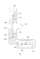
図1は、本実施形態に係る撮像装置10を表す分解斜視図である。図1では、本来撮像装置10を表す場合に必要になる外装カバー等を不図示にしている。本実施形態では、本発明を説明するために必要な部分のみを図示し、その他の部分を不図示として説明に用いる図を簡潔に表現する。また、本実施形態では、便宜上、撮像素子に対して被写体側に向いた方向を前側と呼び、撮影者側に向いた方向を後側と呼ぶことにする。
(First Embodiment)
FIG. 1 is an exploded perspective view showing the
像ブレ補正ユニット200は、シャッタユニット300とともにベース部材400に固定される。そして、ベース部材400と制御基板100は、不図示の外装カバーに固定される構成になっている。像ブレ補正ユニット200は、撮像素子を含む可動ユニットと、可動ユニットを固定保持する固定ユニット(筐体)で構成されている。そして、可動ユニットは、光軸と直交する平面方向に変位することで移動可能であり、光学的な像ブレを補正可能に構成されている。像ブレ補正ユニット200の詳細は後述する。
The
ベース部材400に対してシャッタユニット300を組みつける。その後、像ブレ補正ユニット200は、3本のビス600a、600b、及び600cと3つのコイルばね500a、500b、及び500c(不図示)によってベース部材400に対して光軸方向に若干量変位可能に支持される。そして、ビス600a、600b、及び600cの締め込み量を調整することでベース部材400に対する撮像素子の撮像面の傾きを調整する。調整が完了すると、ビス600a、600b、及び600cの緩みを防止するため像ブレ補正ユニット200の固定ユニットに接着固定される。
The
次に、制御基板100には、撮像信号を制御する制御IC(撮像制御部)101が実装されている。そして、コネクタ102、103、及び104が実装されている。制御基板100には、他にもチップ抵抗やセラミックコンデンサ、インダクタ、トランジスタ等、様々な電子部品が実装されているが、図1においては不図示としている。コネクタ102、103は、像ブレ補正ユニット200から延出するフレキシブルプリント基板と接続して、制御基板100と像ブレ補正ユニット200とを電気的に接続する。そして、コネクタ104は、シャッタユニット300から延出するフレキシブルプリント基板と接続して、制御基板100とシャッタユニット300とを電気的に接続する。
Next, a control IC (imaging control unit) 101 that controls an imaging signal is mounted on the
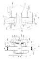
次に、像ブレ補正ユニット200の構成について図2~図4を用いて説明する。図2及び図3は、本実施形態に係る像ブレ補正ユニット200の構成を表す分解斜視図である。図4は、本実施形態に係るフレキシブルプリント基板240の構成を表す正面図である。像ブレ補正ユニット200は、ベース部材400に固定される固定ユニットと、固定ユニットに対して光軸と直交する平面方向に変位可能に保持される可動ユニットとで構成される。まず、固定ユニットは、主に前側ヨーク210と、ベースプレート250と、後側ヨーク260とで構成されている。そして、可動ユニットは、主にセンサホルダ220と、フレキシブルプリント基板240と、フレキシブルプリント基板270とで構成されている。
Next, the configuration of the
センサホルダ220には、撮像素子230と、撮像素子230が実装されているプリント基板231が接着固定されている。そして、センサホルダ220は、撮像素子230よりも前側にローパスフィルタ221が配置されており、赤外線の入射を防止し、色モアレ等の発生を防止する。また、センサホルダ220には、3か所の開口部223a、223b、及び223cが形成されている。そして、フレキシブルプリント基板(第二のフレキシブルプリント基板)240には、3つのコイル(駆動部材)241a、241b、及び241cが搭載されている。フレキシブルプリント基板240は、開口部223a、223b、及び223cに対してコイル241a、241b、及び241cが内部に収容されるように、センサホルダ220に対して後側からフレキシブルプリント基板240を組み込み、接着固定している。
The
次に、センサホルダ220には、3か所の球受け部222a、222b、及び222cが形成されている。前側ヨーク210は、球受け部222a、222b、及び222cと対向する位置に球受け部213a、213b、及び213cが形成されている。撮像素子230とプリント基板231を接着固定した状態のセンサホルダ220は、球受け部同士の間に球体215a、215b、及び215cを挟持することで前側ヨーク210に対してボール支持される。ここで、前側ヨーク210には、不図示の磁石がセンサホルダ220と対向する任意の位置に接着固定されており、対してセンサホルダ220側には、磁石と対向する位置に不図示の強磁性材料(鉄等)の板材が貼り合わされている。そして、センサホルダ220を一定距離まで近接させると、センサホルダ220が前側ヨーク210に磁気吸引されて、球体215a、215b、及び215cを介して、光軸と直交する平面方向に変位可能に保持される。
Next, the
前側ヨーク210には、コイル241a、241b、及び241cと対向する位置に磁石212a、212b、及び212cが貼りつけられている。また、前側ヨーク210には、支柱211a、211b、及び211cがベースプレート250に向けて立設されている。支柱211a、211b、及び211cは、もう一端がベースプレート250に圧入されて、センサホルダ220を挟み込むように、前側ヨーク210とベースプレート250が接合される。
後側ヨーク260には、光軸方向からの平面視において、コイル241a、241b、及び241cと、磁石261a、261b、及び261cとの中心が一致する位置に磁石261a、261b、及び261cが位置決めされて貼りつけられている。そして、ベースプレート250には、光軸方向からの平面視において、磁石261a、261b、及び261cとほぼ同じ位置、形状の開口部251a、251b、及び251cが形成されている。後側ヨーク260は、開口部251a、251b、及び251cに対して、磁石261a、261b、及び261cが内部に収容されるようにベースプレート250に対して後側から後側ヨーク260を装着する。後側ヨーク260及びベースプレート250は、それぞれ強磁性材料で構成されている。そして、磁石261a、261b、及び261cが貼り合わされた後側ヨーク260をベースプレート250に位置合わせして接触させるだけで磁気吸着し、別途接着材料を用いることなく2つの部品の接合が可能である。
さらに、ベースプレート250には、開口部252が形成されている。センサホルダ220を前側ヨーク210とベースプレート250とで挟持すると、開口部252からプリント基板231が後側から露出する。プリント基板231には、コネクタ232が実装されている。そして、フレキシブルプリント基板270にコネクタ(第1コネクタ)271が実装されており、フレキシブルプリント基板270をプリント基板231に対して後側から開口部252を通過するように組み込み、コネクタ232とコネクタ271を嵌合させる。コネクタ232とコネクタ271は、互いに嵌合形状が適合するプラグコネクタとリセプタクルコネクタの関係になっている。
Further, the
フレキシブルプリント基板270は、長尺の板状の形状を成しており、その中央部にコネクタ271が実装されている。そして、コネクタ271の近傍にコネクタ272が実装されており、長尺の長手方向の一方にコネクタ273が実装され、他方にコネクタ274が実装されている。コネクタ273は、制御基板100に実装されているコネクタ102と嵌合形状が適合するプラグコネクタとリセプタクルコネクタの関係になっている。同様に、コネクタ274は、制御基板100に実装されているコネクタ103と嵌合形状が適合するプラグコネクタとリセプタクルコネクタの関係になっている。
The flexible printed
前述のとおり、フレキシブルプリント基板240は、コイル241a、241b、及び241cが接着固定されている。図4に示すフレキシブルプリント基板240には、コイルの巻き線と電気的に接続するための半田付けランド243a、243b、243c、243d、243e、及び243fが形成されている。コイル241aの巻きはじめと巻き終わりの線を半田付けランド243a及び243bに半田付けし、コイル241bの巻きはじめと巻き終わりの線を半田付けランド243c及び243dに半田付けする。そして、コイル241cの巻きはじめと巻き終わりの線を半田付けランド243e及び243fに半田付けすることで、各コイルは、フレキシブルプリント基板240と電気的に接続される。さらに、フレキシブルプリント基板240は、コイル241a、241b、及び241cの巻き線の内側にホール素子242a、242b、及び242cが実装されている。フレキシブルプリント基板240には、コネクタ端子部244が形成されており、各半田付けランドや各ホール素子からの配線パターンがフレキシブルプリント基板240の内部に展開されて、コネクタ端子部244へ接続されている。コネクタ端子部244は、フレキシブルプリント基板270に実装されているコネクタ272に接続することで、フレキシブルプリント基板270を介して制御基板100とフレキシブルプリント基板240が電気的に接続される。
As described above, in the flexible printed
従って、ブレ補正ユニット200は、前側ヨーク210に設置されている磁石212a~212cと後側ヨーク260に設置されている磁石261a~261cとで形成される磁界環境中にコイル241a~241cを配置している。そして、これらのコイルに電流を流すことによって、各コイルにローレンツ力を発生させてこの力を推力としてセンサホルダ220を光軸と直交する平面方向に変位させることが可能な構成としている。また、コイル241a、241b、及び241cの内側に実装されているホール素子242a、242b、及び242cによって、センサホルダ220が磁石212a、212b、及び212cに対して相対的に移動することによる磁力の変化が検出される。そして、固定ユニットに対する可動ユニットの光軸と直交する平面方向の変位量を検出することができる。
Therefore, the
次に、フレキシブルプリント基板270の構成について、図5を用いて説明する。図5は、本実施形態に係るフレキシブルプリント基板270の構成を表す図である。本実施形態では、便宜上、像ブレ補正ユニット200を組み立てた状態において、撮像素子230に対してコイル241cが搭載されている方向を下側と呼び、その反対方向を上側と呼ぶことにする。
Next, the configuration of the flexible printed
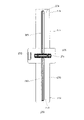
フレキシブルプリント基板270は、前述のとおりコネクタ271とコネクタ231とが嵌合することでプリント基板231と電気的に接続し、可動ユニットに固定される。図5(A)では、フレキシブルプリント基板270が可動ユニットに固定されている状態を後側から俯瞰している図である。フレキシブルプリント基板270は、大別すると5つの領域で構成されて、3つの剛体部分(接続部)と剛体部分同士をつなぐ可撓部分(配線部)とで構成される。
As described above, the flexible printed
まず、第一の接続部275と、第二の接続部278と、第三の接続部279には、ガラスエポキシ樹脂などの絶縁補強材料を熱硬化性接着剤などで貼り合わせることで剛性を持たせている。そして、補強材料を貼り合わせている面とは反対の面に対して、基板間接続コネクタを実装している。第一の接続部275には、コネクタ271及びコネクタ272を実装している。第二の接続部278には、コネクタ273を実装している。そして、第三の接続部279にはコネクタ274を実装している。次に、第一の接続部275と第二の接続部278の間には、可撓性を有し、且つコネクタ271及び272とコネクタ273を電気的に接続している第一の配線部276が形成(延在)されている。さらに、第一の接続部275と第三の接続部279の間には、可撓性を有し、且つコネクタ271及び272とコネクタ274を電気的に接続している第二の配線部277が形成(延在)されている。ここで、フレキシブルプリント基板270は、第一の配線部276の配線長さL1と、第二の配線部277の配線長さL2が同じ長さになるように構成されている。さらに、第一の配線部276の外形幅W1と、第二の配線部277の外形幅W2が同じ幅になるように構成されている。
First, the
次に、図5(B)は、フレキシブルプリント基板270のコネクタ273、274が制御基板100側に実装されているコネクタ102、103と嵌合して電気的に接続されている状態を後側から俯瞰している図である。前述のとおり、像ブレ補正ユニット200は、シャッタユニット300とともにベース部材400に固定される。そして、ベース部材400と制御基板100は、不図示の外装カバーに固定される構成になっている。図5(B)は、制御基板100、像ブレ補正ユニット200、シャッタユニット300、及びベース部材400が不図示の外装カバーに組み込まれた後、フレキシブルプリント基板270と制御基板100とを電気的に接続した状態を表している。
Next, FIG. 5B shows a state in which the
この状態において、制御基板100の外側の下方向から第一の配線部276を延出し、制御基板100の上方向(反対の外側)から第二の配線部277を延出する。そして、後側に湾曲させてコネクタ(第2コネクタ)273とコネクタ(第4コネクタ)102を嵌合させ、コネクタ(第3コネクタ)274とコネクタ(第5コネクタ)103を嵌合させている。フレキシブルプリント基板270は、第一の配線部276と第二の配線部277とで制御基板100の一部を覆い囲うように配線される構成になっている。つまり、フレキシブルプリント基板270は、第一の配線部276と第二の配線部277とで制御基板100を抱きかかえるように構成される。撮像装置10の後側からの投影視において、第一の接続部275と第一の配線部276の境界部と、第二の接続部278と第一の配線部276の境界部との上下方向の距離をL3とする。そして、第一の接続部275と第二の配線部277の境界部と、第三の接続部279と第二の配線部277の境界部との上下方向の距離をL4とする。この場合、フレキシブルプリント基板270及び制御基板100は、L3とL4が同じ距離になるように構成されている。
In this state, the
第一の配線部276の配線長さL1と、第二の配線部277の配線長さL2が同じ長さになるように構成して、且つ第一の配線部276の外形幅W1と、第二の配線部277の外形幅W2が同じ幅になるように構成する。さらに、L3とL4を同じ距離になるように構成する。これにより、第一の配線部276と、第二の配線部277を第一の接続部275の中心から上下対称な形状で制御基板100に固定保持することができる。具体的には、第一の接続部275に対して撮像装置10の下方向から配線される第一の配線部276と、第一の接続部275に対して撮像装置10の上方向から配線される第二の配線部277を制御基板100に固定保持することができる。
The wiring length L1 of the
以上から、可動ユニットを上下方向に並進駆動させる場合の中心から上方向へ駆動させる際のフレキシブルプリント基板270の変形で生じる負荷と下方向へ駆動させる際のフレキシブルプリント基板270の変形で生じる負荷をほぼ等しくすることができる。同様に、可動ユニットを左右方向に並進駆動させる場合の中心から右方向へ駆動させる際のフレキシブルプリント基板270の変形で生じる負荷と左方向へ駆動させる際のフレキシブルプリント基板270の変形で生じる負荷をほぼ等しくすることができる。例えば、第一の配線部276の配線長さL1が本実施形態の構成よりも短く構成されている場合、フレキシブルプリント基板270の変形によって生じる負荷のバランスが上下方向で不均等になってしまう。そして、この状態で上方向に可動ユニットを駆動させると、負荷のバランスが均等になっている場合と比較して単位変位量に対して発生するフレキの負荷がより大きな負荷になってしまう。この構成では、可動ユニットを高精度に制御するために必要になる磁石の大きさやコイルの大きさが大型化してしまい、撮像装置10の大型化を招く虞がある。また、制御するために必要な消費電力も増大してしまう虞がある。したがって、フレキシブルプリント基板270が対称形状になるように制御基板100に結線させる本実施形態の構成は撮像装置10の小型化、消費電力低減に寄与する。
From the above, the load caused by the deformation of the flexible printed
また、図5(A)において、光軸中心Pは、撮像装置10における光軸中心を表している。フレキシブルプリント基板270は、光軸中心Pから第一の接続部275と第一の配線部276との境界までの上下方向の距離をX1、光軸中心Pから第一の接続部275と第二の配線部277との境界までの上下方向の距離をX2とする。この場合、X1とX2が等しくなるように構成してよい。従って、可動ユニットが光軸中心Pを回転中心として時計回りに回転駆動する際のフレキシブルプリント基板270の変形で生じる負荷と、反時計回りに回転駆動する際のフレキシブルプリント基板270の変形で生じる負荷をほぼ等しくすることができる。フレキシブルプリント基板270を対称形状に構成し、且つ光軸中心Pを対称の起点にすることによって、可動ユニットを並進駆動させることで発生する負荷だけでなく、可動ユニットを回転駆動させることにで発生する負荷のバランス調整も行うことができる。従ってて、上述の構成は、撮像装置10の小型化、消費電力低減により好適である。なお、本実施形態では、フレキシブルプリント基板240に3つのコイル(駆動部材)241a、241b、及び241cが搭載されている構成としている。しかしながら、これに限定することなく、例えば、第一の接続部275の外形の一部が延出することでフレキシブルプリント基板270が3つのコイル241a、241b、及び241cを搭載可能な駆動部材搭載部を有してもよい。そして、第一の配線部276と第二の配線部277の両方、或いは第一の配線部276と第二の配線部277の何れか一方を介して、3つのコイルと、制御基板100とが電気的に接続される構成としてもよい。
Further, in FIG. 5A, the optical axis center P represents the optical axis center in the
次に、撮像装置10の内部で展開される配線パターンについて図6及び図7を用いて説明する。図6は、本実施形態に係るフレキシブルプリント基板270の内部に展開される配線パターンを表す平面図である。そして、図7は、本実施形態に係る制御基板100の内部に展開される配線パターンを表す平面図である。
Next, the wiring pattern developed inside the
図6において、フレキシブルプリント基板270には、第一の接続部275に実装されているコネクタ271から第一の配線部276を介して第二の接続部278に実装されているコネクタ273まで電気的に接続されている高速伝送配線280が形成されている。更に、コネクタ271から第二の配線部277を介して第三の接続部279に実装されているコネクタ274まで電気的に接続されている高速伝送配線281が形成されている。この高速伝送配線280及び281は、例えば、LVDS(Low Voltage Differential Signal:低電圧差動信号)等の伝送方式を採用した、2本の信号線を1対とする伝送路である。本実施形態に係る撮像装置10は、この高速伝送配線280及び281を使って撮像素子と制御基板との間で撮像信号伝送が行われ、撮像信号の高速伝送に対応している。フレキシブルプリント基板270には、高速伝送配線280及び281以外にもグランド配線や撮像素子を駆動させる電源配線等も配線されているが、図6では不図示としている。
In FIG. 6, the flexible printed
本実施形態では、第一の配線部276に配線される高速伝送配線(第一の差動信号配線パターン)280として、3対の差動伝送配線が配線されている。そして、第二の配線部277に配線される高速伝送配線(第二の差動信号配線パターン)281として、3対の差動伝送配線が配線されている。コネクタ271は、互いに平行な2列の信号端子列を有しており、第一の配線部276側に近接する信号端子列に対して高速伝送配線280の信号が割り当てられるように撮像素子230を実装するプリント基板231の内部配線が設計されている。さらに、第二の配線部277側に近接する信号端子列に対して高速伝送配線281の信号が割り当てられるように、プリント基板231の内部配線が設計されている。コネクタ273及び274は、コネクタ271と同様に、互いに平行な2列の信号端子列を有する構造を成している。フレキシブルプリント基板270は、積層構造が多層の層構成を有しており、本実施形態では、2層構成としている。そして、コネクタ271が実装されている面とは反対側の面にコネクタ273、及び274が実装されている。高速伝送配線280は、コネクタ271の信号端子列から配線が延出し、コネクタ273の平行な2列の信号端子列の内、コネクタ271から見て奥側の端子列に配置される信号端子列と電気的に接続されている。具体的には、コネクタ273の裏面を高速伝送配線280が通過した後、スルーホールによってコネクタ273が実装されている側の面に配線されている伝送路と電気的に接続し、コネクタ271から見て奥側の端子列に配置される信号端子と接続する。同様に、高速伝送配線281は、コネクタ271から見て奥側にあるコネクタ274の信号端子列に配置される信号端子と電気的に接続する構成になっている。
In the present embodiment, three pairs of differential transmission wirings are wired as high-speed transmission wirings (first differential signal wiring pattern) 280 to be wired to the
ここで、前述のとおり、フレキシブルプリント基板270は、第一の配線部276と第二の配線部277が同じ配線長さになるように形成されており、高速伝送配線280及び281も各対をなす高速伝送路がほぼ等しい配線長さになるように形成されている。高速伝送路において、同期をとることを必要とする複数の電気信号を伝送する場合、配線による遅延時間の差が十分小さくなるように、複数の電気信号が伝送される配線それぞれの長さが等しくなるように構成する等長配線を行うことが望ましい。したがって、高速伝送配線280及び281を等長配線で構成することは高速伝送品質を確保するうえで有益に作用する。また、コネクタ273に近い列に結線されている高速伝送配線280をコネクタ273側に延出させて、且つコネクタ274に近い列に結線されている高速伝送配線281をコネクタ274側に配線を延出させる。これににより、コネクタ271を実装している近傍の高速伝送配線を簡潔な構成として、異なる差動配線対とのクリアランスを適正量確保することによって、隣接パターン間におけるクロストーク、及び裏面パターンとのクロストークの低減を図ることができる。
Here, as described above, the flexible printed
次に、図7によると、制御基板100に実装されているコネクタ102及び103の間に矩形状のパッケージ外形をなす制御IC101が実装されている。制御IC101には、複数の信号端子(複数の電極部)が形成されており、制御基板100と半田接合されて制御基板100と電気的に接続されている。制御基板100には、コネクタ102から制御IC101の信号端子の一部まで電気的に接続されている高速伝送配線(第三の差動信号配線パターン)105が形成されている。更に、コネクタ103から制御IC101の信号端子の一部まで電気的に接続されている高速伝送配線(第四の差動信号配線パターン)106が形成されている。高速伝送配線105は、フレキシブルプリント基板270の内部を配線される高速伝送配線280に対してコネクタ273、及びコネクタ102を介して電気的に接続されている。そして、高速伝送配線106は、フレキシブルプリント基板270の内部を配線される高速伝送配線281に対してコネクタ274及びコネクタ103を介して電気的に接続されている。高速伝送配線105及び106は、高速伝送配線280、及び281と同様の差動伝送路を形成している。制御基板100には、高速伝送配線105及び106以外にも様々な信号配線やグランド配線が展開されているが、図7では不図示としている。
Next, according to FIG. 7, a
制御基板100は、積層構造が多層の層構成を有しており、例えば、複数層のコア層の両面にビルドアップ層を積層したビルドアップ基板や、全ての積層において層間ビアによる接続構造が可能なANY-LAYER基板などが例示される。高速伝送配線105及び106は、コネクタ102及び103の信号端子列から制御基板100の表層を配線が延出し、そのまま制御IC101の信号端子の一部に接続されるように構成されている。制御基板100は、基板の厚さを比較的薄く形成し、且つ、多数の導体層を積層する場合には隣接する導体層同士のクリアランスがより近接することになる。
The
この構成において、ある層を高速伝送路が配線されると、その配線層に隣接する導体層両面に対して、投影上、高速伝送路と重なる領域に対してグランドプレーンのみを形成する、或いは導体層の全てまたは一部をエッチング除去する等の措置をとる。これにより、高速伝送路のインピーダンスを適正に管理することができる。これらの措置は、導体層の一定量の面積を占めてしまい、基板配線の制約に繋がってしまう。制御IC101は、撮像信号を制御するICであり、多くの信号線や電源線が制御IC101の信号端子に接続されており、制御IC101の直下の配線密度は、非常に高密度に配線されている場合が多い。高速伝送配線105及び106を制御基板100の表層を使って配線することによって、高速伝送路のインピーダンスを一定に管理するために所定の措置を要する導体層は、1つ内側の内層一層のみで対処可能になるため、基板配線の自由度を高めることができる。また、高速伝送配線105及び106は、それぞれの差動伝送路がほぼ等しい配線長さになるように形成されている。高速伝送配線280及び281と同様に、差動伝送路を等長配線で構成することによって高速伝送品質を確保するうえで有益に作用することができる。
In this configuration, when a high-speed transmission line is wired in a certain layer, only a ground plane is formed in a region overlapping the high-speed transmission line in terms of projection on both sides of the conductor layer adjacent to the wiring layer, or a conductor. Take measures such as etching and removing all or part of the layer. This makes it possible to properly manage the impedance of the high-speed transmission line. These measures occupy a certain area of the conductor layer, which leads to restrictions on the board wiring. The
なお、可動ユニットを構成するフレキシブルプリント基板270と、フレキシブルプリント基板240とは、別体に形成する必要はなく、一体的な形状をなしてもよい。この場合、双方を電気的に接続しているコネクタ272を省略することができる。また、図7では、制御IC101のパッケージ辺に対してほぼ平行に且つ等間隔に信号端子列が配列されているが、パッケージの信号端子配置は、図示されている構成に限定されない。例えば、制御基板100の表層配線で接続可能な信号配列であれば、いずれの信号配列であっても、不均一な信号配置であっても本発明の目的は達成される。そして、制御IC101は、例えば、図7の状態から45度回転した位相で制御基板100に実装されていてもよい。この場合、コネクタ103及び104それぞれに近接する制御IC101の2辺にわたって配置されている一部の信号端子が高速伝送配線105及び106と電気的に接続されることで、より効率的に制御基板100での高速伝送路配線を行うことができる。また、各基板間の接続部品としてプラグコネクタとリセプタクルコネクタのコネクタを採用することは必須の構成ではなく、フレキシブルプリント基板270の配線長さL1及びL2を等しい長さで形成する等の本実施形態の要旨に沿った範囲で適宜変更が可能である。例えば、フレキシブルプリント基板270の両端に実装されるコネクタ273及び274を廃止し、コネクタ端子部を形成し、制御基板100に対してコネクタ端子部が適合するコネクタを実装するように構成してもよい。
The flexible printed
(第2実施形態)
次に、本実施形態について図8を用いて以下に説明する。なお、第1実施形態で説明した撮像装置10の構成要素と同じ部分については、同じ符号を用いて、その詳細な説明は省略する。図8は、本実施形態における像ブレ補正ユニット700の構成を表す図である。像ブレ補正ユニット700は、第1実施形態で説明した像ブレ補正ユニット200に対して後側ヨーク260を後側ヨーク265へ組み替えられている。そして、フレキシブルプリント基板270がフレキシブルプリント基板770に組み替えられている。後側ヨーク265は、外形形状がコの字状に形成された平板形状を成している。後側ヨーク265には、光軸方向からの平面視において、後側ヨーク260と同様にコイル241a~241cと磁石261a~261cとの中心が一致する位置に磁石261a~261cが位置決めされて貼りつけられている。後側ヨーク265は、強磁性材料で構成されており、開口部251a~251cに対して、磁石261a~261cが内部に収容されるようにベースプレート250に対して後側から装着され、磁気吸着によりベースプレート250に接合される。
(Second Embodiment)
Next, this embodiment will be described below with reference to FIG. The same reference numerals are used for the same parts as the components of the
フレキシブルプリント基板770は、長尺の板状の形状を成しており、その中央部にコネクタ271が実装されている。そして、コネクタ271の近傍にコネクタ272が実装されており、フレキシブルプリント基板770をプリント基板231に対して後側から開口部252を通過するように組み込み、コネクタ232とコネクタ271を嵌合させて可動ユニットに組み込まれる。そして、コネクタ端子部244がコネクタ272接続されて、フレキシブルプリント基板240とフレキシブルプリント基板770が電気的に接続される。また、長尺の長手方向の一方にはコネクタ273、他方にはコネクタ274が実装されている。コネクタ273は、制御基板100に実装されているコネクタ102と嵌合形状が適合するプラグコネクタとリセプタクルコネクタの関係になっている。同様に、コネクタ274は、制御基板100に実装されているコネクタ103と嵌合形状が適合するプラグコネクタとリセプタクルコネクタの関係になっている。
The flexible printed
フレキシブルプリント基板770は、3つの剛体部分(接続部)を有し、第一の接続部775には、コネクタ271及びコネクタ272を実装している。第二の接続部782には、コネクタ273を実装している。そして、第三の接続部783には、コネクタ274を実装している。次に、第一の接続部775と第二の接続部782との間には、第一の固定部778が形成されており、後側ヨーク265に固定接合されている。そして、第一の接続部775と第三の接続部783との間には、第二の固定部779が形成されており、後側ヨーク265に固定接合される。第一の固定部778及び第二の固定部779には、それぞれ後側ヨーク265に対して位置合わせを行う穴が空けられており、治具などを用いて後側ヨーク265に位置合わせを行った後、両面テープや接着剤等によって後側ヨーク265に固定接合される。
The flexible printed
次に、第一の接続部775と第一の固定部778との間には、可撓性を有する配線領域である第一の配線部776が形成されている。そして、第一の接続部775と第二の固定部779との間には、可撓性を有する配線領域である第二の配線部777が形成されている。更に、第一の固定部778と第二の接続部782との間には、可撓性を有する配線領域である第三の配線部780が形成されている。そして、第二の固定部779と第三の接続部783との間には可撓性を有する配線領域である第四の配線部781が形成されている。フレキシブルプリント基板770には、第一の接続部775に実装されているコネクタ271から第一の配線部776及び第三の配線部780を介して第二の接続部782に実装されているコネクタ273まで電気的に接続される不図示の配線路が形成されている。更に、コネクタ271から第二の配線部777及び第四の配線部781を介して第三の接続部783に実装されているコネクタ274まで電気的に接続される不図示の配線路が形成されている。
Next, a
ここで、フレキシブルプリント基板770は、第一の配線部776の配線長さと、第二の配線部777の配線長さが同じ長さになるように構成されている。そして、第一の配線部776は一定量の撓みを形成した状態で第一の固定部778に接続されて撓み形状が維持される。同様に、第二の配線部777は、一定量の撓みを形成した状態で第二の固定部779に接続されて撓み形状が維持される。ここで、第一の接続部775と第一の配線部776との境界から第一の固定部778までの距離L5は、第一の接続部775と第二の配線部777との境界から第二の固定部779までの距離L6が等しくなるように像ブレ補正ユニット700は構成されている。第一の接続部775と第一の配線部776との境界から第一の固定部778と第一の配線部776との境界までの距離が、第一の接続部775と第二の配線部777との境界から第二の固定部779と第二の配線部777との境界までの距離と、同じ距離に形成される。更に、第一の配線部776の外形幅W3と、第二の配線部777の外形幅W4が同じ幅になるように構成されている。ここで、第一の配線部776及び第二の配線部777に形成される撓み量は、可動ユニットの変位量が最も光軸中心から離れた位置に達した場合、第一の配線部776及び第二の配線部777がに延びきってしまうことがない。そして、ともに一定量の撓み量を維持することができるように設定される。
Here, the flexible printed
第一の配線部776の配線長さと、第二の配線部777の配線長さが同じ長さになるように構成し、且つ第一の配線部776の外形幅W3と、第二の配線部777の外形幅W4が同じ幅になるように構成する。さらに、第一の配線部776と第二の配線部777の撓み量を等しくなるように構成する。これにより、第一の接続部775と第二の配線部777を第一の接続部の中心から上下対称な形状で制御基板100に固定保持することができる。従って、可動ユニットを上下方向に並進駆動させる場合の中心から上方向へ駆動させる際のフレキシブルプリント基板770の変形で生じる負荷と下方向へ駆動させる際のフレキシブルプリント基板770の変形で生じる負荷をほぼ等しくすることができる。同様に、可動ユニットを左右方向に並進駆動させる場合の中心から右方向へ駆動させる際のフレキシブルプリント基板770の変形で生じる負荷と左方向へ駆動させる際のフレキシブルプリント基板770の変形で生じる負荷をほぼ等しくすることができる。以上のように、像ブレ補正ユニット700を構成することは、像ブレ補正ユニット700のサイズを最適化し、可動ユニットを制御するために必要な消費電力の低減に寄与する。また、二つの配線路は、互いの配線長さが同じ長さになるように形成されている。この二つの配線路を使って高速伝送路を形成し、同期をとることを必要とする複数の電気信号を伝送する場合、配線による遅延時間の差が十分小さくなるように、複数の電気信号が伝送される配線それぞれの長さが等しくなるような等長配線を行うことが望ましい。従って、高速伝送路を等長配線で構成することは高速伝送品質を確保するうえで有益に作用する。
The wiring length of the
また、図8において、フレキシブルプリント基板770は、光軸中心Pから第一の接続部775と第一の配線部776との境界までの上下方向の距離をX3とする。そして、光軸中心Pから第一の接続部775と第二の配線部777との境界までの上下方向の距離をX4とする。この場合、X3とX4が等しくなるようにフレキシブルプリント基板770を構成してもよい。従って、可動ユニットが光軸中心Pを回転中心として時計回りに回転駆動する際のフレキシブルプリント基板270の変形で生じる負荷と、反時計回りに回転駆動する際のフレキシブルプリント基板770の変形で生じる負荷をほぼ等しくすることができる。フレキシブルプリント基板770を対称形状に構成し、且つ光軸中心Pを対称の起点にする。これにより、可動ユニットを並進駆動させることによって発生する負荷だけではなく、可動ユニットを回転駆動させることによって発生する負荷のバランス調整も行うことができる。従って、上述の構成は撮像装置10の小型化、消費電力低減により好適に作用する。
Further, in FIG. 8, in the flexible printed
なお、可動ユニットを構成するフレキシブルプリント基板770と、フレキシブルプリント基板240とは、別体に形成する必要はなく、一体的な形状をなしてもよい。この場合、双方を電気的に接続しているコネクタ272を省略することができる。また、本実施形態では、第一の固定部778と第二の固定部779との間で可動ユニットの変位によるフレキシブルプリント基板770の変形が発生する構成になっている。そして、第一の配線部776及び第二の配線部777には、例えば、図8に記載のように配線路と平行な方向に沿ったスリットを形成する等、フレキシブルプリント基板770の変形によって生じる負荷を低減させる措置を適宜講じる。このことは、像ブレ補正ユニット700を高精度に制御するうえで好適に作用する。また、第一の固定部778と第二の固定部779との間で可動ユニットの変位によるフレキシブルプリント基板770の変形が発生する構成になっている。このため、第三の配線部780及び第四の配線部781は、互いに同一形状にする必要はなく、制御基板100の部品配置の自由度を向上させることができる。そして、フレキシブルプリント基板770の内部に配線される高速伝送路を等長配線で揃えつつ、第三の配線部780及び第四の配線部781を適宜好適な形状にする。これにより、高速伝送路の伝送品質を確保しつつ、制御基板100の部品配置、配線の自由度を向上させることができる。
The flexible printed
(第3実施形態)
次に、本実施形態について図9~図11を用いて以下に説明する。なお、第1実施形態及び第2実施形態で説明した撮像装置10の構成要素と同じ部分については、同じ符号を用いて、その詳細な説明は省略する。図9~図11は、本実施形態における像ブレ補正ユニット800の構成を表す斜視図である。像ブレ補正ユニット800は、第1実施形態で説明した像ブレ補正ユニット200に対してフレキシブルプリント基板240がフレキシブルプリント基板810へ組み替えられている。そして、後側ヨーク260を後側ヨーク830へ組み替えられている。そして、フレキシブルプリント基板270がフレキシブルプリント基板840に組み替えられている。更に熱移送部材820と、放熱板850が組み込まれている。また、制御基板100から制御基板150に組み替えられる。
(Third Embodiment)
Next, this embodiment will be described below with reference to FIGS. 9 to 11. The same reference numerals are used for the same parts as the components of the
後側ヨーク830には、光軸方向からの平面視において、後側ヨーク260と同様にコイル241a~241cと磁石261a~261cとの中心が一致する位置に磁石261a~261cが位置決めされて貼りつけられている。後側ヨーク830は、強磁性材料で構成されており、開口部251a~251cに対して、磁石261a~261cが内部に収容されるようにベースプレート250に対して後側から装着され、磁気吸着によりベースプレート250に接合される。
フレキシブルプリント基板840は、長尺の板状の形状を成しており、その中央部にコネクタ271が実装されている。そして、フレキシブルプリント基板840をプリント基板231に対して後側から開口部252を通過するように組み込み、コネクタ232とコネクタ271を嵌合させて可動ユニットに組み込まれる。また、長尺の長手方向の一方には、コネクタ841、他方にはコネクタ842が実装されている。コネクタ841及び842は、制御基板150に実装されているコネクタとそれぞれ嵌合して、像ブレ補正ユニット800と制御基板150を電気的に接続する。フレキシブルプリント基板840には、コネクタ272は搭載されておらず、コイルやホール素子を実装するフレキシブルプリント基板810は直接制御基板150に接続される構成になっている。
The flexible printed
可動ユニットにフレキシブルプリント基板840を組み込んだ後、放熱板850を後側から像ブレ補正ユニット800に組み込む。放熱板850は、後側ヨーク830に形成されている位置決め穴に対して、対向する位置に位置決めピンが打たれている。ピンと穴の嵌合により、放熱板850は、後側ヨーク830に対して位置決めされて両面テープ、接着剤、或いはビス等の任意の固定手段によって固定される。プリント基板231及びセンサホルダ220には、予め熱移送部材820が組み込まれている。この熱移送部材820は、熱伝導性の優れた材料が含まれており、例えば、グラファイトカーボン材やシリコンゲル、金属発泡剤、多孔質結晶体、グラファイトシート等、またはこれらの組み合わせで構成されている。
After incorporating the flexible printed
熱移送部材820は、撮像素子230の発熱によってプリント基板231及びセンサホルダ220へ伝熱する熱量を撮像装置10内部に熱移送する機能を担う。具体的には、二本の熱移送部821及び822によって、撮像素子230の発熱を接合部823へ熱移送させる。熱移送部821及び822は、可撓性を有し、更に高い柔軟性を有する構成が採用される。例えば、グラファイトシートをベースとして両面を薄手の保護フィルムで密封加工したシート等である。接合部(第二の接合部)823は、放熱板850に対して両面テープ等の接合材料で固定保持されている。より好適には、熱伝導性の高い部材による接合が望ましい。この熱移送部材820によって、可動ユニットから固定ユニットへの熱移送が行われる。
The
次に、フレキシブルプリント基板810は、第1実施形態と同様にコイル241a、241b、及び241cとホール素子242a、242b、及び242cを実装しており、これらの配線がコネクタ端子部815まで延出している。そして、制御基板150に接続される経路の途中で、放熱板850に対して、接合部(第一の接合部)813が両面テープ等の接合材料で固定保持されている。コイルやホール素子の部品実装部と接合部813との間は細い腕状の配線部811及び812によって配線がつながっている。接合部813の端部には、更に配線部814が形成されており、二つの配線部811及び812に配線されている信号線が合流し、コネクタ端子部815に接続されている。制御基板150が組み込まれた後、制御基板150に実装されているコネクタ152に対してコネクタ端子部815が嵌合してフレキシブルプリント基板810と制御基板150が電気的に接続される構成になっている。
Next, the flexible printed
熱移送部材820の熱移送部821及び822とフレキシブルプリント基板810の配線部811及び812の延出方向は、フレキシブルプリント基板840の配線部の延出方向に対して直交する方向に延出する構成になっている。そして、可動ユニットが変位すると、熱移送部材820の熱移送部821及び822とフレキシブルプリント基板810の配線部811及び812が変形して可動ユニットの動きに追従するように構成されている。ここで、熱移送部821及び822の厚さや幅の設定は、配線部811及び812の厚さや幅を考慮して設定されている。具体的には、例えば、可動ユニットを上下方向に並進駆動させる場合に熱移送部821及び822の変形によって生じる負荷と、配線部811及び812の変形によって生じる負荷がほぼ等しくなるように設定されている。同様に、可動ユニットを左右方向に並進駆動させる場合に配線部811及び812の変形によって生じる負荷がほぼ等しくなるように設定されている。フレキシブルプリント基板810は、複数のコイル及びホール素子の配線が展開されている。そして、フレキシブルプリント基板840のように撮像素子230の撮像信号や電源ライン等を配線しておらず、相対的に配線本数を少なく構成できるため、可動ユニットの変位によって配線部811及び812が変形して生じる負荷も相対的に小さい。そのため、熱移送部821及び822の幅寸法を配線部811及び812と同じ寸法に揃えるだけでも可動ユニットの変位によって生じる負荷のバランスをとる効果を得ることができる。
The extension directions of the
また、本発明の好ましい実施形態について説明したが、本発明は、これらの実施形態に限定されず、その要旨の範囲内で種々の変形および変更が可能である。 Moreover, although the preferred embodiment of the present invention has been described, the present invention is not limited to these embodiments, and various modifications and modifications can be made within the scope of the gist thereof.
10 撮像装置
100 制御基板
230 撮像素子
231 プリント基板
270 フレキシブルプリント基板
275 第一の接続部
276 第一の配線部
277 第二の配線部
278 第二の接続部
279 第三の接続部
10
Claims (13)
前記可動ユニットに固定され、撮像素子を実装する基板と、
前記基板と電気的に接続されるフレキシブルプリント基板と、
前記筐体に固定され、光軸と直交する平面に対して前記基板と平行に配置されて前記フレキシブルプリント基板を介して前記基板と電気的に接続される制御基板と、
を備え、
前記フレキシブルプリント基板は、
前記基板と接続するための第一の接続部と、
可撓性を有し、前記第一の接続部を中心として対称な方向に延在し、前記第一の接続部から等しい長さ及びほぼ等しい幅を有する第一の配線部及び第二の配線部と、
前記第一の配線部の端部に設けられ、前記制御基板と接続されるための第二の接続部と、
前記第二の配線部の端部に設けられ、前記制御基板と接続されるための第三の接続部と
を備え、
前記撮像素子の有効画素中心が前記光軸の中心と一致する姿勢において、前記第一の配線部及び前記第二の配線部を湾曲させて、前記第二の接続部及び前記第三の接続部を前記制御基板と電気的に接続した状態で、前記第一の接続部と前記第一の配線部との境界から前記第二の接続部と前記第一の配線部との境界までの距離が、前記第一の接続部と前記第二の配線部との境界から前記第三の接続部と前記第二の配線部との境界までの距離と、同じ距離に形成し、
前記フレキシブルプリント基板は、前記撮像素子と前記制御基板を電気的に接続する複数の差動信号配線パターンをさらに備え、
前記複数の差動信号配線パターンは、前記第一の配線部に配線される第一の差動信号配線パターンと、前記第二の配線部に配線される第二の差動信号配線パターンとは、伝送路がほぼ等しい長さになるように形成されている
ことを特徴とする撮像装置。 An imaging device having a housing and a movable unit that can move in a direction orthogonal to the optical axis with respect to the housing.
A substrate fixed to the movable unit and mounting an image sensor,
A flexible printed circuit board that is electrically connected to the board,
A control board fixed to the housing, arranged parallel to the board with respect to a plane orthogonal to the optical axis, and electrically connected to the board via the flexible printed circuit board.
Equipped with
The flexible printed substrate is
The first connection part for connecting to the board and
A first and second wiring that is flexible, extends symmetrically about the first connection, and has the same length and width from the first connection. Department and
A second connection portion provided at the end of the first wiring portion and for connecting to the control board,
A third connection portion provided at the end of the second wiring portion and for connecting to the control board is provided.
In a posture in which the effective pixel center of the image pickup element coincides with the center of the optical axis, the first wiring portion and the second wiring portion are curved to form the second connection portion and the third connection portion. Is electrically connected to the control board, and the distance from the boundary between the first connection portion and the first wiring portion to the boundary between the second connection portion and the first wiring portion is , The distance from the boundary between the first connection portion and the second wiring portion to the boundary between the third connection portion and the second wiring portion is formed at the same distance.
The flexible printed circuit board further includes a plurality of differential signal wiring patterns that electrically connect the image pickup device and the control board.
The plurality of differential signal wiring patterns are a first differential signal wiring pattern wired to the first wiring portion and a second differential signal wiring pattern wired to the second wiring portion. , The transmission lines are formed so that they have almost the same length.
An imaging device characterized by this.
前記可動ユニットに固定され、撮像素子を実装する基板と、
前記基板と電気的に接続されるフレキシブルプリント基板と、
前記筐体に固定され、光軸と直交する平面に対して前記基板と平行に配置されて前記フレキシブルプリント基板を介して前記基板と電気的に接続される制御基板と、
を備え、
前記フレキシブルプリント基板は、
前記基板と接続するための第一の接続部と、
可撓性を有し、前記第一の接続部を中心として対称な方向に延在し、前記第一の接続部から等しい長さ及びほぼ等しい幅を有する第一の配線部及び第二の配線部と、
前記第一の配線部の端部に設けられ、前記制御基板と接続されるための第二の接続部と、
前記第二の配線部の端部に設けられ、前記制御基板と接続されるための第三の接続部と、
前記第一の接続部と前記第二の接続部との間に形成され、前記筐体に固定保持される第一の固定部と、
前記第一の接続部と前記第三の接続部との間に形成され、前記筐体に固定保持される第二の固定部と
を備え、
前記撮像素子の有効画素中心が前記光軸の中心と一致する姿勢において、前記第一の配線部及び前記第二の配線部を湾曲させて、前記第二の接続部及び前記第三の接続部を前記制御基板と電気的に接続した状態で、前記第一の接続部と前記第一の配線部との境界から前記第一の固定部と前記第一の配線部との境界までの距離が、前記第一の接続部と前記第二の配線部との境界から前記第二の固定部と前記第二の配線部との境界までの距離と、同じ距離に形成し、
前記フレキシブルプリント基板は、前記撮像素子と前記制御基板を電気的に接続する複数の差動信号配線パターンをさらに備え、
前記複数の差動信号配線パターンは、前記第一の配線部に配線される第一の差動信号配線パターンと、前記第二の配線部に配線される第二の差動信号配線パターンとは、伝送路がほぼ等しい長さになるように形成されている
ことを特徴とする撮像装置。 An imaging device having a housing and a movable unit that can move in a direction orthogonal to the optical axis with respect to the housing.
A substrate fixed to the movable unit and mounting an image sensor,
A flexible printed circuit board that is electrically connected to the board,
A control board fixed to the housing, arranged parallel to the board with respect to a plane orthogonal to the optical axis, and electrically connected to the board via the flexible printed circuit board.
Equipped with
The flexible printed substrate is
The first connection part for connecting to the board and
A first and second wiring that is flexible, extends symmetrically about the first connection, and has the same length and width from the first connection. Department and
A second connection portion provided at the end of the first wiring portion and for connecting to the control board,
A third connection portion provided at the end of the second wiring portion and for connecting to the control board,
A first fixing portion formed between the first connecting portion and the second connecting portion and fixedly held in the housing,
A second fixing portion formed between the first connecting portion and the third connecting portion and fixedly held in the housing is provided.
In a posture in which the effective pixel center of the image pickup element coincides with the center of the optical axis, the first wiring portion and the second wiring portion are curved to form the second connection portion and the third connection portion. Is electrically connected to the control board, and the distance from the boundary between the first connection portion and the first wiring portion to the boundary between the first fixing portion and the first wiring portion is , The distance from the boundary between the first connecting portion and the second wiring portion to the boundary between the second fixed portion and the second wiring portion is formed at the same distance.
The flexible printed circuit board further includes a plurality of differential signal wiring patterns that electrically connect the image pickup device and the control board.
The plurality of differential signal wiring patterns are a first differential signal wiring pattern wired to the first wiring portion and a second differential signal wiring pattern wired to the second wiring portion. , The transmission lines are formed so that they have almost the same length.
An imaging device characterized by this.
ことを特徴とする請求項1または2に記載の撮像装置。 In the second connection portion and the third connection portion, the first wiring portion and the second wiring portion are curved so as to be opposite to the surface facing the flexible printed circuit board from the outside of the control board. The image pickup apparatus according to claim 1 or 2 , wherein the image pickup device is connected to the control board in terms of.
ことを特徴とする請求項1~3のいずれか1項に記載の撮像装置。 The image pickup apparatus according to any one of claims 1 to 3, wherein the center of the first connection portion and the center of the optical axis are arranged at coincident positions.
前記撮像制御部は、前記第二の接続部及び前記第三の接続部と接続する面に配置され、前記第二の接続部から前記撮像制御部までの距離が、前記第三の接続部から前記撮像制御部までの距離と同じ距離になる
ことを特徴とする請求項1~4のいずれか1項に記載の撮像装置。 The control board has an image pickup control unit that is electrically connected to the plurality of differential signal wiring patterns and controls the image pickup element.
The image pickup control unit is arranged on a surface connecting to the second connection unit and the third connection unit, and the distance from the second connection unit to the image pickup control unit is from the third connection unit. The imaging device according to any one of claims 1 to 4, wherein the distance is the same as the distance to the imaging control unit.
前記複数の電極部の内、前記撮像制御部の端部に近接する電極部の一部が前記差動信号配線パターンと電気的に接続する
ことを特徴とする請求項5に記載の撮像装置。 The image pickup control unit has a plurality of electrode units that are formed in a rectangular shape and are electrically connected to the control board.
The image pickup apparatus according to claim 5 , wherein a part of the electrode part close to the end portion of the image pickup control unit is electrically connected to the differential signal wiring pattern among the plurality of electrode parts.
前記制御基板は、積層構造が多層の層構成を有しており、前記第三の差動信号配線パターンと前記第四の差動信号配線パターンは、前記第二及び第三の接続部から前記制御基板の前記撮像制御部が搭載されている側の表層を配線が延出して、前記複数の電極部の一部に接続されるように構成される
ことを特徴とする請求項6に記載の撮像装置。 A third differential signal wiring pattern for connecting a part of the plurality of electrode portions to the first differential signal wiring pattern, and a second differential signal wiring from a part of the plurality of electrode portions. A fourth differential signal wiring pattern for connecting to the pattern is formed on the control board.
The control board has a multi-layered structure, and the third differential signal wiring pattern and the fourth differential signal wiring pattern are described from the second and third connection portions. The sixth aspect of claim 6 , wherein the wiring extends from the surface layer of the control board on the side on which the image pickup control unit is mounted so as to be connected to a part of the plurality of electrode units. Imaging device.
前記可動ユニットに固定され、撮像素子を実装する基板と、
前記基板と電気的に接続されるフレキシブルプリント基板と、
前記筐体に固定され、光軸と直交する平面に対して前記基板と平行に配置されて前記フレキシブルプリント基板を介して前記基板と電気的に接続される制御基板と、
を備え、
前記フレキシブルプリント基板は、
前記基板と接続するための第一の接続部と、
可撓性を有し、前記第一の接続部を中心として対称な方向に延在し、前記第一の接続部から等しい長さ及びほぼ等しい幅を有する第一の配線部及び第二の配線部と、
前記第一の配線部の端部に設けられ、前記制御基板と接続されるための第二の接続部と、
前記第二の配線部の端部に設けられ、前記制御基板と接続されるための第三の接続部と
を備え、
前記撮像素子の有効画素中心が前記光軸の中心と一致する姿勢において、前記第一の配線部及び前記第二の配線部を湾曲させて、前記第二の接続部及び前記第三の接続部を前記制御基板と電気的に接続した状態で、前記第一の接続部と前記第一の配線部との境界から前記第二の接続部と前記第一の配線部との境界までの距離が、前記第一の接続部と前記第二の配線部との境界から前記第三の接続部と前記第二の配線部との境界までの距離と、同じ距離に形成し、
前記可動ユニットは、前記筐体に対して前記可動ユニットを相対的に駆動させる駆動部材と、前記駆動部材を搭載し、前記駆動部材と電気的に接続されている第二のフレキシブルプリント基板とを有し、
前記フレキシブルプリント基板は、前記第一の接続部の近傍、或いは前記第一の接続部の内部であって、前記第一の配線部と、前記第二の配線部との間に第四の接続部を有し、
前記第二のフレキシブルプリント基板は、前記第四の接続部において、前記フレキシブルプリント基板と電気的に接続し、前記フレキシブルプリント基板を介して前記駆動部材と、前記制御基板と、が電気的に接続される
ことを特徴とする撮像装置。 An imaging device having a housing and a movable unit that can move in a direction orthogonal to the optical axis with respect to the housing.
A substrate fixed to the movable unit and mounting an image sensor,
A flexible printed circuit board that is electrically connected to the board,
A control board fixed to the housing, arranged parallel to the board with respect to a plane orthogonal to the optical axis, and electrically connected to the board via the flexible printed circuit board.
Equipped with
The flexible printed substrate is
The first connection part for connecting to the board and
A first and second wiring that is flexible, extends symmetrically about the first connection, and has the same length and width from the first connection. Department and
A second connection portion provided at the end of the first wiring portion and for connecting to the control board,
With a third connection portion provided at the end of the second wiring portion and for connecting to the control board.
Equipped with
In a posture in which the effective pixel center of the image pickup element coincides with the center of the optical axis, the first wiring portion and the second wiring portion are curved to form the second connection portion and the third connection portion. Is electrically connected to the control board, and the distance from the boundary between the first connection portion and the first wiring portion to the boundary between the second connection portion and the first wiring portion is , The distance from the boundary between the first connection portion and the second wiring portion to the boundary between the third connection portion and the second wiring portion is formed at the same distance.
The movable unit includes a drive member that drives the movable unit relative to the housing, and a second flexible printed substrate on which the drive member is mounted and electrically connected to the drive member. Have and
The flexible printed board is in the vicinity of the first connection portion or inside the first connection portion, and is a fourth connection between the first wiring portion and the second wiring portion. Has a part,
The second flexible printed circuit board is electrically connected to the flexible printed circuit board at the fourth connection portion, and the drive member and the control board are electrically connected via the flexible printed circuit board. An imaging device characterized by being
前記可動ユニットに固定され、撮像素子を実装する基板と、
前記基板と電気的に接続されるフレキシブルプリント基板と、
前記筐体に固定され、光軸と直交する平面に対して前記基板と平行に配置されて前記フレキシブルプリント基板を介して前記基板と電気的に接続される制御基板と、
を備え、
前記フレキシブルプリント基板は、
前記基板と接続するための第一の接続部と、
可撓性を有し、前記第一の接続部を中心として対称な方向に延在し、前記第一の接続部から等しい長さ及びほぼ等しい幅を有する第一の配線部及び第二の配線部と、
前記第一の配線部の端部に設けられ、前記制御基板と接続されるための第二の接続部と、
前記第二の配線部の端部に設けられ、前記制御基板と接続されるための第三の接続部と、
前記第一の接続部と前記第二の接続部との間に形成され、前記筐体に固定保持される第一の固定部と、
前記第一の接続部と前記第三の接続部との間に形成され、前記筐体に固定保持される第二の固定部と
を備え、
前記撮像素子の有効画素中心が前記光軸の中心と一致する姿勢において、前記第一の配線部及び前記第二の配線部を湾曲させて、前記第二の接続部及び前記第三の接続部を前記制御基板と電気的に接続した状態で、前記第一の接続部と前記第一の配線部との境界から前記第一の固定部と前記第一の配線部との境界までの距離が、前記第一の接続部と前記第二の配線部との境界から前記第二の固定部と前記第二の配線部との境界までの距離と、同じ距離に形成し、
前記可動ユニットは、前記筐体に対して前記可動ユニットを相対的に駆動させる駆動部材と、前記駆動部材を搭載し、前記駆動部材と電気的に接続されている第二のフレキシブルプリント基板とを有し、
前記フレキシブルプリント基板は、前記第一の接続部の近傍、或いは前記第一の接続部の内部であって、前記第一の配線部と、前記第二の配線部との間に第四の接続部を有し、
前記第二のフレキシブルプリント基板は、前記第四の接続部において、前記フレキシブルプリント基板と電気的に接続し、前記フレキシブルプリント基板を介して前記駆動部材と、前記制御基板と、が電気的に接続される
ことを特徴とする撮像装置。 An imaging device having a housing and a movable unit that can move in a direction orthogonal to the optical axis with respect to the housing.
A substrate fixed to the movable unit and mounting an image sensor,
A flexible printed circuit board that is electrically connected to the board,
A control board fixed to the housing, arranged parallel to the board with respect to a plane orthogonal to the optical axis, and electrically connected to the board via the flexible printed circuit board.
Equipped with
The flexible printed substrate is
The first connection part for connecting to the board and
A first and second wiring that is flexible, extends symmetrically about the first connection, and has the same length and width from the first connection. Department and
A second connection portion provided at the end of the first wiring portion and for connecting to the control board,
A third connection portion provided at the end of the second wiring portion and for connecting to the control board,
A first fixing portion formed between the first connecting portion and the second connecting portion and fixedly held in the housing,
A second fixing portion formed between the first connection portion and the third connection portion and fixedly held in the housing.
Equipped with
In a posture in which the effective pixel center of the image pickup element coincides with the center of the optical axis, the first wiring portion and the second wiring portion are curved to form the second connection portion and the third connection portion. Is electrically connected to the control board, and the distance from the boundary between the first connection portion and the first wiring portion to the boundary between the first fixing portion and the first wiring portion is , The distance from the boundary between the first connecting portion and the second wiring portion to the boundary between the second fixed portion and the second wiring portion is formed at the same distance.
The movable unit includes a drive member that drives the movable unit relative to the housing, and a second flexible printed substrate on which the drive member is mounted and electrically connected to the drive member. Have and
The flexible printed board is in the vicinity of the first connection portion or inside the first connection portion, and is a fourth connection between the first wiring portion and the second wiring portion. Has a part,
The second flexible printed circuit board is electrically connected to the flexible printed circuit board at the fourth connection portion, and the drive member and the control board are electrically connected via the flexible printed circuit board. An imaging device characterized by being
前記可動ユニットに固定され、撮像素子を実装する基板と、
前記基板と電気的に接続されるフレキシブルプリント基板と、
前記筐体に固定され、光軸と直交する平面に対して前記基板と平行に配置されて前記フレキシブルプリント基板を介して前記基板と電気的に接続される制御基板と、
を備え、
前記フレキシブルプリント基板は、
前記基板と接続するための第一の接続部と、
可撓性を有し、前記第一の接続部を中心として対称な方向に延在し、前記第一の接続部から等しい長さ及びほぼ等しい幅を有する第一の配線部及び第二の配線部と、
前記第一の配線部の端部に設けられ、前記制御基板と接続されるための第二の接続部と、
前記第二の配線部の端部に設けられ、前記制御基板と接続されるための第三の接続部と
を備え、
前記撮像素子の有効画素中心が前記光軸の中心と一致する姿勢において、前記第一の配線部及び前記第二の配線部を湾曲させて、前記第二の接続部及び前記第三の接続部を前記制御基板と電気的に接続した状態で、前記第一の接続部と前記第一の配線部との境界から前記第二の接続部と前記第一の配線部との境界までの距離が、前記第一の接続部と前記第二の配線部との境界から前記第三の接続部と前記第二の配線部との境界までの距離と、同じ距離に形成し、
前記フレキシブルプリント基板は、前記筐体に対して前記可動ユニットを相対的に駆動させる駆動部材を搭載可能な駆動部材搭載部を有し、
前記第一の接続部の外形の一部が延出することで前記駆動部材搭載部を形成し、前記第一の配線部と前記第二の配線部の両方、或いは前記第一の配線部と前記第二の配線部の何れか一方を介して、前記駆動部材と、前記制御基板とが電気的に接続される
ことを特徴とする撮像装置。 An imaging device having a housing and a movable unit that can move in a direction orthogonal to the optical axis with respect to the housing.
A substrate fixed to the movable unit and mounting an image sensor,
A flexible printed circuit board that is electrically connected to the board,
A control board fixed to the housing, arranged parallel to the board with respect to a plane orthogonal to the optical axis, and electrically connected to the board via the flexible printed circuit board.
Equipped with
The flexible printed substrate is
The first connection part for connecting to the board and
A first and second wiring that is flexible, extends symmetrically about the first connection, and has the same length and width from the first connection. Department and
A second connection portion provided at the end of the first wiring portion and for connecting to the control board,
With a third connection portion provided at the end of the second wiring portion and for connecting to the control board.
Equipped with
In a posture in which the effective pixel center of the image pickup element coincides with the center of the optical axis, the first wiring portion and the second wiring portion are curved to form the second connection portion and the third connection portion. Is electrically connected to the control board, and the distance from the boundary between the first connection portion and the first wiring portion to the boundary between the second connection portion and the first wiring portion is , The distance from the boundary between the first connection portion and the second wiring portion to the boundary between the third connection portion and the second wiring portion is formed at the same distance.
The flexible printed board has a drive member mounting portion on which a drive member that drives the movable unit relative to the housing can be mounted.
A part of the outer shape of the first connection portion extends to form the drive member mounting portion, and the first wiring portion and the second wiring portion, or the first wiring portion and the same. An image pickup apparatus characterized in that the drive member and the control board are electrically connected via any one of the second wiring portions.
前記可動ユニットに固定され、撮像素子を実装する基板と、A substrate fixed to the movable unit and mounting an image sensor,
前記基板と電気的に接続されるフレキシブルプリント基板と、A flexible printed circuit board that is electrically connected to the board,
前記筐体に固定され、光軸と直交する平面に対して前記基板と平行に配置されて前記フレキシブルプリント基板を介して前記基板と電気的に接続される制御基板と、A control board fixed to the housing, arranged parallel to the board with respect to a plane orthogonal to the optical axis, and electrically connected to the board via the flexible printed circuit board.
を備え、Equipped with
前記フレキシブルプリント基板は、The flexible printed substrate is
前記基板と接続するための第一の接続部と、The first connection part for connecting to the board and
可撓性を有し、前記第一の接続部を中心として対称な方向に延在し、前記第一の接続部から等しい長さ及びほぼ等しい幅を有する第一の配線部及び第二の配線部と、A first and second wiring that is flexible, extends symmetrically about the first connection, and has the same length and width from the first connection. Department and
前記第一の配線部の端部に設けられ、前記制御基板と接続されるための第二の接続部と、A second connection portion provided at the end of the first wiring portion and for connecting to the control board,
前記第二の配線部の端部に設けられ、前記制御基板と接続されるための第三の接続部と、A third connection portion provided at the end of the second wiring portion and for connecting to the control board,
前記第一の接続部と前記第二の接続部との間に形成され、前記筐体に固定保持される第一の固定部と、A first fixing portion formed between the first connecting portion and the second connecting portion and fixedly held in the housing,
前記第一の接続部と前記第三の接続部との間に形成され、前記筐体に固定保持される第二の固定部とA second fixing portion formed between the first connection portion and the third connection portion and fixedly held in the housing.
を備え、Equipped with
前記撮像素子の有効画素中心が前記光軸の中心と一致する姿勢において、前記第一の配線部及び前記第二の配線部を湾曲させて、前記第二の接続部及び前記第三の接続部を前記制御基板と電気的に接続した状態で、前記第一の接続部と前記第一の配線部との境界から前記第一の固定部と前記第一の配線部との境界までの距離が、前記第一の接続部と前記第二の配線部との境界から前記第二の固定部と前記第二の配線部との境界までの距離と、同じ距離に形成し、In a posture in which the effective pixel center of the image pickup element coincides with the center of the optical axis, the first wiring portion and the second wiring portion are curved to form the second connection portion and the third connection portion. Is electrically connected to the control board, and the distance from the boundary between the first connection portion and the first wiring portion to the boundary between the first fixing portion and the first wiring portion is , The distance from the boundary between the first connecting portion and the second wiring portion to the boundary between the second fixed portion and the second wiring portion is formed at the same distance.
前記フレキシブルプリント基板は、前記筐体に対して前記可動ユニットを相対的に駆動させる駆動部材を搭載可能な駆動部材搭載部を有し、The flexible printed board has a drive member mounting portion on which a drive member that drives the movable unit relative to the housing can be mounted.
前記第一の接続部の外形の一部が延出することで前記駆動部材搭載部を形成し、前記第一の配線部と前記第二の配線部の両方、或いは前記第一の配線部と前記第二の配線部の何れか一方を介して、前記駆動部材と、前記制御基板とが電気的に接続されるA part of the outer shape of the first connection portion extends to form the drive member mounting portion, and the first wiring portion and the second wiring portion, or the first wiring portion and the same. The drive member and the control board are electrically connected via either one of the second wiring portions.
ことを特徴とする撮像装置。An imaging device characterized by this.
前記可動ユニットに固定され、撮像素子を実装する基板と、A substrate fixed to the movable unit and mounting an image sensor,
前記基板と電気的に接続されるフレキシブルプリント基板と、A flexible printed circuit board that is electrically connected to the board,
前記筐体に固定され、光軸と直交する平面に対して前記基板と平行に配置されて前記フレキシブルプリント基板を介して前記基板と電気的に接続される制御基板と、A control board fixed to the housing, arranged parallel to the board with respect to a plane orthogonal to the optical axis, and electrically connected to the board via the flexible printed circuit board.
を備え、Equipped with
前記フレキシブルプリント基板は、The flexible printed substrate is
前記基板と接続するための第一の接続部と、The first connection part for connecting to the board and
可撓性を有し、前記第一の接続部を中心として対称な方向に延在し、前記第一の接続部から等しい長さ及びほぼ等しい幅を有する第一の配線部及び第二の配線部と、A first and second wiring that is flexible, extends symmetrically about the first connection, and has the same length and width from the first connection. Department and
前記第一の配線部の端部に設けられ、前記制御基板と接続されるための第二の接続部と、A second connection portion provided at the end of the first wiring portion and for connecting to the control board,
前記第二の配線部の端部に設けられ、前記制御基板と接続されるための第三の接続部とWith a third connection portion provided at the end of the second wiring portion and for connecting to the control board.
を備え、Equipped with
前記撮像素子の有効画素中心が前記光軸の中心と一致する姿勢において、前記第一の配線部及び前記第二の配線部を湾曲させて、前記第二の接続部及び前記第三の接続部を前記制御基板と電気的に接続した状態で、前記第一の接続部と前記第一の配線部との境界から前記第二の接続部と前記第一の配線部との境界までの距離が、前記第一の接続部と前記第二の配線部との境界から前記第三の接続部と前記第二の配線部との境界までの距離と、同じ距離に形成し、In a posture in which the effective pixel center of the image pickup element coincides with the center of the optical axis, the first wiring portion and the second wiring portion are curved to form the second connection portion and the third connection portion. Is electrically connected to the control board, and the distance from the boundary between the first connection portion and the first wiring portion to the boundary between the second connection portion and the first wiring portion is , The distance from the boundary between the first connection portion and the second wiring portion to the boundary between the third connection portion and the second wiring portion is formed at the same distance.
前記可動ユニットは、前記筐体に対して前記可動ユニットを相対的に駆動させる駆動部材と、前記駆動部材を搭載し、前記駆動部材と電気的に接続されている第三のフレキシブルプリント基板と、前記可動ユニットの一部に一端を接合し、もう一端を前記筐体の一部に接合して、前記可動ユニットと前記筐体との間で熱移送を可能に構成される熱移送部材と、を有し、The movable unit includes a drive member that drives the movable unit relative to the housing, and a third flexible printed substrate on which the drive member is mounted and electrically connected to the drive member. A heat transfer member configured by joining one end to a part of the movable unit and joining the other end to a part of the housing to enable heat transfer between the movable unit and the housing. Have,
前記フレキシブルプリント基板と前記制御基板との間に前記筐体に固定された放熱板を備え、A heat sink fixed to the housing is provided between the flexible printed circuit board and the control board.
前記第三のフレキシブルプリント基板は、前記放熱板と接合する第一の接合部を有し、前記熱移送部材は、前記放熱板と接合する第二の接合部を有し、The third flexible printed substrate has a first joining portion to be joined to the heat sink, and the heat transfer member has a second joining portion to be joined to the heat sink.
光軸方向からの投影視において、前記第三のフレキシブルプリント基板は、前記第一の配線部が延出する方向に対して直交する方向に延出して前記放熱板に固定保持され、且つ前記熱移送部材は、前記第三のフレキシブルプリント基板が延出する方向に対向する方向から延出して前記放熱板に固定保持されるIn the projection view from the optical axis direction, the third flexible printed circuit board extends in a direction orthogonal to the extending direction of the first wiring portion, is fixedly held by the heat sink, and has the heat. The transfer member extends from the direction facing the extending direction of the third flexible printed substrate and is fixedly held by the heat sink.
ことを特徴とする撮像装置。An imaging device characterized by this.
前記可動ユニットに固定され、撮像素子を実装する基板と、A substrate fixed to the movable unit and mounting an image sensor,
前記基板と電気的に接続されるフレキシブルプリント基板と、A flexible printed circuit board that is electrically connected to the board,
前記筐体に固定され、光軸と直交する平面に対して前記基板と平行に配置されて前記フレキシブルプリント基板を介して前記基板と電気的に接続される制御基板と、A control board fixed to the housing, arranged parallel to the board with respect to a plane orthogonal to the optical axis, and electrically connected to the board via the flexible printed circuit board.
を備え、Equipped with
前記フレキシブルプリント基板は、The flexible printed substrate is
前記基板と接続するための第一の接続部と、The first connection part for connecting to the board and
可撓性を有し、前記第一の接続部を中心として対称な方向に延在し、前記第一の接続部から等しい長さ及びほぼ等しい幅を有する第一の配線部及び第二の配線部と、A first and second wiring that is flexible, extends symmetrically about the first connection, and has the same length and width from the first connection. Department and
前記第一の配線部の端部に設けられ、前記制御基板と接続されるための第二の接続部と、A second connection portion provided at the end of the first wiring portion and for connecting to the control board,
前記第二の配線部の端部に設けられ、前記制御基板と接続されるための第三の接続部と、A third connection portion provided at the end of the second wiring portion and for connecting to the control board,
前記第一の接続部と前記第二の接続部との間に形成され、前記筐体に固定保持される第一の固定部と、A first fixing portion formed between the first connecting portion and the second connecting portion and fixedly held in the housing,
前記第一の接続部と前記第三の接続部との間に形成され、前記筐体に固定保持される第二の固定部とA second fixing portion formed between the first connection portion and the third connection portion and fixedly held in the housing.
を備え、Equipped with
前記撮像素子の有効画素中心が前記光軸の中心と一致する姿勢において、前記第一の配線部及び前記第二の配線部を湾曲させて、前記第二の接続部及び前記第三の接続部を前記制御基板と電気的に接続した状態で、前記第一の接続部と前記第一の配線部との境界から前記第一の固定部と前記第一の配線部との境界までの距離が、前記第一の接続部と前記第二の配線部との境界から前記第二の固定部と前記第二の配線部との境界までの距離と、同じ距離に形成し、In a posture in which the effective pixel center of the image pickup element coincides with the center of the optical axis, the first wiring portion and the second wiring portion are curved to form the second connection portion and the third connection portion. Is electrically connected to the control board, and the distance from the boundary between the first connection portion and the first wiring portion to the boundary between the first fixing portion and the first wiring portion is , The distance from the boundary between the first connecting portion and the second wiring portion to the boundary between the second fixed portion and the second wiring portion is formed at the same distance.
前記可動ユニットは、前記筐体に対して前記可動ユニットを相対的に駆動させる駆動部材と、前記駆動部材を搭載し、前記駆動部材と電気的に接続されている第三のフレキシブルプリント基板と、前記可動ユニットの一部に一端を接合し、もう一端を前記筐体の一部に接合して、前記可動ユニットと前記筐体との間で熱移送を可能に構成される熱移送部材と、を有し、The movable unit includes a drive member that drives the movable unit relative to the housing, and a third flexible printed substrate on which the drive member is mounted and electrically connected to the drive member. A heat transfer member configured by joining one end to a part of the movable unit and joining the other end to a part of the housing to enable heat transfer between the movable unit and the housing. Have,
前記フレキシブルプリント基板と前記制御基板との間に前記筐体に固定された放熱板を備え、A heat sink fixed to the housing is provided between the flexible printed circuit board and the control board.
前記第三のフレキシブルプリント基板は、前記放熱板と接合する第一の接合部を有し、前記熱移送部材は、前記放熱板と接合する第二の接合部を有し、The third flexible printed substrate has a first joining portion to be joined to the heat sink, and the heat transfer member has a second joining portion to be joined to the heat sink.
光軸方向からの投影視において、前記第三のフレキシブルプリント基板は、前記第一の配線部が延出する方向に対して直交する方向に延出して前記放熱板に固定保持され、且つ前記熱移送部材は、前記第三のフレキシブルプリント基板が延出する方向に対向する方向から延出して前記放熱板に固定保持されるIn the projection view from the optical axis direction, the third flexible printed circuit board extends in a direction orthogonal to the extending direction of the first wiring portion, is fixedly held by the heat sink, and has the heat. The transfer member extends from the direction facing the extending direction of the third flexible printed substrate and is fixedly held by the heat sink.
ことを特徴とする撮像装置。An imaging device characterized by this.
Priority Applications (1)
| Application Number | Priority Date | Filing Date | Title |
|---|---|---|---|
| JP2018095427A JP7098413B2 (en) | 2018-05-17 | 2018-05-17 | Imaging device |
Applications Claiming Priority (1)
| Application Number | Priority Date | Filing Date | Title |
|---|---|---|---|
| JP2018095427A JP7098413B2 (en) | 2018-05-17 | 2018-05-17 | Imaging device |
Publications (3)
| Publication Number | Publication Date |
|---|---|
| JP2019200349A JP2019200349A (en) | 2019-11-21 |
| JP2019200349A5 JP2019200349A5 (en) | 2021-07-26 |
| JP7098413B2 true JP7098413B2 (en) | 2022-07-11 |
Family
ID=68612479
Family Applications (1)
| Application Number | Title | Priority Date | Filing Date |
|---|---|---|---|
| JP2018095427A Active JP7098413B2 (en) | 2018-05-17 | 2018-05-17 | Imaging device |
Country Status (1)
| Country | Link |
|---|---|
| JP (1) | JP7098413B2 (en) |
Families Citing this family (6)
| Publication number | Priority date | Publication date | Assignee | Title |
|---|---|---|---|---|
| JP7483354B2 (en) * | 2019-11-27 | 2024-05-15 | キヤノン株式会社 | Imaging device |
| JP7520549B2 (en) | 2020-03-30 | 2024-07-23 | キヤノン株式会社 | Electronics |
| JP7137610B2 (en) * | 2020-12-21 | 2022-09-14 | ジョウシュウシ レイテック オプトロニクス カンパニーリミテッド | Anti-vibration mechanisms for imaging devices, optical systems, cameras and electronic devices |
| JP7108676B2 (en) * | 2020-12-21 | 2022-07-28 | ジョウシュウシ レイテック オプトロニクス カンパニーリミテッド | Anti-vibration mechanisms for imaging devices, optical systems, cameras and electronic devices |
| JP7463412B2 (en) * | 2022-01-07 | 2024-04-08 | 維沃移動通信有限公司 | Sensor shift type optical image stabilization actuator and camera module |
| WO2024053255A1 (en) * | 2022-09-06 | 2024-03-14 | 富士フイルム株式会社 | Image blur correction device and imaging device |
Citations (5)
| Publication number | Priority date | Publication date | Assignee | Title |
|---|---|---|---|---|
| JP2006031023A (en) | 2004-07-21 | 2006-02-02 | Hewlett-Packard Development Co Lp | Method of compensating for effect of temperature on control system |
| JP2010192749A (en) | 2009-02-19 | 2010-09-02 | Konica Minolta Opto Inc | Flexible printed circuit board and image blur correcting device using the same, imaging apparatus, and method of fabricating flexible printed circuit board |
| JP2010286567A (en) | 2009-06-09 | 2010-12-24 | Tamron Co Ltd | Shake correction mechanism and image capturing apparatus |
| JP2013044960A (en) | 2011-08-24 | 2013-03-04 | Nikon Corp | Vibration isolator, lens barrel, and optical device |
| JP2015075658A (en) | 2013-10-09 | 2015-04-20 | 株式会社ニコン | Optical device |
Family Cites Families (2)
| Publication number | Priority date | Publication date | Assignee | Title |
|---|---|---|---|---|
| JPH0447774A (en) * | 1990-06-14 | 1992-02-17 | Canon Inc | Image pickup device |
| JPH0980516A (en) * | 1995-09-14 | 1997-03-28 | Nikon Corp | Image blurring correction device |
-
2018
- 2018-05-17 JP JP2018095427A patent/JP7098413B2/en active Active
Patent Citations (5)
| Publication number | Priority date | Publication date | Assignee | Title |
|---|---|---|---|---|
| JP2006031023A (en) | 2004-07-21 | 2006-02-02 | Hewlett-Packard Development Co Lp | Method of compensating for effect of temperature on control system |
| JP2010192749A (en) | 2009-02-19 | 2010-09-02 | Konica Minolta Opto Inc | Flexible printed circuit board and image blur correcting device using the same, imaging apparatus, and method of fabricating flexible printed circuit board |
| JP2010286567A (en) | 2009-06-09 | 2010-12-24 | Tamron Co Ltd | Shake correction mechanism and image capturing apparatus |
| JP2013044960A (en) | 2011-08-24 | 2013-03-04 | Nikon Corp | Vibration isolator, lens barrel, and optical device |
| JP2015075658A (en) | 2013-10-09 | 2015-04-20 | 株式会社ニコン | Optical device |
Also Published As
| Publication number | Publication date |
|---|---|
| JP2019200349A (en) | 2019-11-21 |
Similar Documents
| Publication | Publication Date | Title |
|---|---|---|
| JP7098413B2 (en) | Imaging device | |
| JP7520549B2 (en) | Electronics | |
| US11050913B2 (en) | Integrated substrate for anti-shake apparatus | |
| US10725314B2 (en) | Optical image stabilization (OIS) unit of a camera module | |
| JP6711370B2 (en) | Substrate, imaging unit and imaging device | |
| JP2023100676A (en) | Imaging device and electronic apparatus | |
| US11317027B2 (en) | Imaging unit and imaging apparatus | |
| CN111147706B (en) | Image pickup apparatus having movable unit and control unit | |
| US20220329713A1 (en) | Imaging apparatus | |
| JP7483354B2 (en) | Imaging device | |
| JP2022082426A (en) | Module and device | |
| JP2023157249A (en) | Imaging apparatus | |
| JP2021190953A (en) | Imaging device | |
| WO2007094234A1 (en) | Imaging device |
Legal Events
| Date | Code | Title | Description |
|---|---|---|---|
| A521 | Request for written amendment filed |
Free format text: JAPANESE INTERMEDIATE CODE: A523 Effective date: 20210511 |
|
| A621 | Written request for application examination |
Free format text: JAPANESE INTERMEDIATE CODE: A621 Effective date: 20210511 |
|
| A977 | Report on retrieval |
Free format text: JAPANESE INTERMEDIATE CODE: A971007 Effective date: 20220124 |
|
| A131 | Notification of reasons for refusal |
Free format text: JAPANESE INTERMEDIATE CODE: A131 Effective date: 20220201 |
|
| A521 | Request for written amendment filed |
Free format text: JAPANESE INTERMEDIATE CODE: A523 Effective date: 20220325 |
|
| TRDD | Decision of grant or rejection written | ||
| A01 | Written decision to grant a patent or to grant a registration (utility model) |
Free format text: JAPANESE INTERMEDIATE CODE: A01 Effective date: 20220531 |
|
| A61 | First payment of annual fees (during grant procedure) |
Free format text: JAPANESE INTERMEDIATE CODE: A61 Effective date: 20220629 |
|
| R151 | Written notification of patent or utility model registration |
Ref document number: 7098413 Country of ref document: JP Free format text: JAPANESE INTERMEDIATE CODE: R151 |