JP7085472B2 - Light emitting unit, liquid crystal module, display device and lighting device - Google Patents
Light emitting unit, liquid crystal module, display device and lighting device Download PDFInfo
- Publication number
- JP7085472B2 JP7085472B2 JP2018519113A JP2018519113A JP7085472B2 JP 7085472 B2 JP7085472 B2 JP 7085472B2 JP 2018519113 A JP2018519113 A JP 2018519113A JP 2018519113 A JP2018519113 A JP 2018519113A JP 7085472 B2 JP7085472 B2 JP 7085472B2
- Authority
- JP
- Japan
- Prior art keywords
- display device
- light
- support substrate
- display panel
- emitting unit
- Prior art date
- Legal status (The legal status is an assumption and is not a legal conclusion. Google has not performed a legal analysis and makes no representation as to the accuracy of the status listed.)
- Active
Links
Images


Classifications
-
- G—PHYSICS
- G02—OPTICS
- G02B—OPTICAL ELEMENTS, SYSTEMS OR APPARATUS
- G02B6/00—Light guides; Structural details of arrangements comprising light guides and other optical elements, e.g. couplings
- G02B6/0001—Light guides; Structural details of arrangements comprising light guides and other optical elements, e.g. couplings specially adapted for lighting devices or systems
- G02B6/0011—Light guides; Structural details of arrangements comprising light guides and other optical elements, e.g. couplings specially adapted for lighting devices or systems the light guides being planar or of plate-like form
- G02B6/0081—Mechanical or electrical aspects of the light guide and light source in the lighting device peculiar to the adaptation to planar light guides, e.g. concerning packaging
- G02B6/0086—Positioning aspects
- G02B6/0088—Positioning aspects of the light guide or other optical sheets in the package
-
- G—PHYSICS
- G02—OPTICS
- G02F—OPTICAL DEVICES OR ARRANGEMENTS FOR THE CONTROL OF LIGHT BY MODIFICATION OF THE OPTICAL PROPERTIES OF THE MEDIA OF THE ELEMENTS INVOLVED THEREIN; NON-LINEAR OPTICS; FREQUENCY-CHANGING OF LIGHT; OPTICAL LOGIC ELEMENTS; OPTICAL ANALOGUE/DIGITAL CONVERTERS
- G02F1/00—Devices or arrangements for the control of the intensity, colour, phase, polarisation or direction of light arriving from an independent light source, e.g. switching, gating or modulating; Non-linear optics
- G02F1/01—Devices or arrangements for the control of the intensity, colour, phase, polarisation or direction of light arriving from an independent light source, e.g. switching, gating or modulating; Non-linear optics for the control of the intensity, phase, polarisation or colour
- G02F1/13—Devices or arrangements for the control of the intensity, colour, phase, polarisation or direction of light arriving from an independent light source, e.g. switching, gating or modulating; Non-linear optics for the control of the intensity, phase, polarisation or colour based on liquid crystals, e.g. single liquid crystal display cells
- G02F1/133—Constructional arrangements; Operation of liquid crystal cells; Circuit arrangements
- G02F1/1333—Constructional arrangements; Manufacturing methods
- G02F1/133308—Support structures for LCD panels, e.g. frames or bezels
-
- G—PHYSICS
- G02—OPTICS
- G02F—OPTICAL DEVICES OR ARRANGEMENTS FOR THE CONTROL OF LIGHT BY MODIFICATION OF THE OPTICAL PROPERTIES OF THE MEDIA OF THE ELEMENTS INVOLVED THEREIN; NON-LINEAR OPTICS; FREQUENCY-CHANGING OF LIGHT; OPTICAL LOGIC ELEMENTS; OPTICAL ANALOGUE/DIGITAL CONVERTERS
- G02F1/00—Devices or arrangements for the control of the intensity, colour, phase, polarisation or direction of light arriving from an independent light source, e.g. switching, gating or modulating; Non-linear optics
- G02F1/01—Devices or arrangements for the control of the intensity, colour, phase, polarisation or direction of light arriving from an independent light source, e.g. switching, gating or modulating; Non-linear optics for the control of the intensity, phase, polarisation or colour
- G02F1/13—Devices or arrangements for the control of the intensity, colour, phase, polarisation or direction of light arriving from an independent light source, e.g. switching, gating or modulating; Non-linear optics for the control of the intensity, phase, polarisation or colour based on liquid crystals, e.g. single liquid crystal display cells
- G02F1/133—Constructional arrangements; Operation of liquid crystal cells; Circuit arrangements
- G02F1/1333—Constructional arrangements; Manufacturing methods
- G02F1/1335—Structural association of cells with optical devices, e.g. polarisers or reflectors
- G02F1/1336—Illuminating devices
- G02F1/133602—Direct backlight
- G02F1/133608—Direct backlight including particular frames or supporting means
-
- G—PHYSICS
- G02—OPTICS
- G02F—OPTICAL DEVICES OR ARRANGEMENTS FOR THE CONTROL OF LIGHT BY MODIFICATION OF THE OPTICAL PROPERTIES OF THE MEDIA OF THE ELEMENTS INVOLVED THEREIN; NON-LINEAR OPTICS; FREQUENCY-CHANGING OF LIGHT; OPTICAL LOGIC ELEMENTS; OPTICAL ANALOGUE/DIGITAL CONVERTERS
- G02F1/00—Devices or arrangements for the control of the intensity, colour, phase, polarisation or direction of light arriving from an independent light source, e.g. switching, gating or modulating; Non-linear optics
- G02F1/01—Devices or arrangements for the control of the intensity, colour, phase, polarisation or direction of light arriving from an independent light source, e.g. switching, gating or modulating; Non-linear optics for the control of the intensity, phase, polarisation or colour
- G02F1/13—Devices or arrangements for the control of the intensity, colour, phase, polarisation or direction of light arriving from an independent light source, e.g. switching, gating or modulating; Non-linear optics for the control of the intensity, phase, polarisation or colour based on liquid crystals, e.g. single liquid crystal display cells
- G02F1/133—Constructional arrangements; Operation of liquid crystal cells; Circuit arrangements
- G02F1/1333—Constructional arrangements; Manufacturing methods
- G02F1/133308—Support structures for LCD panels, e.g. frames or bezels
- G02F1/133317—Intermediate frames, e.g. between backlight housing and front frame
-
- G—PHYSICS
- G02—OPTICS
- G02F—OPTICAL DEVICES OR ARRANGEMENTS FOR THE CONTROL OF LIGHT BY MODIFICATION OF THE OPTICAL PROPERTIES OF THE MEDIA OF THE ELEMENTS INVOLVED THEREIN; NON-LINEAR OPTICS; FREQUENCY-CHANGING OF LIGHT; OPTICAL LOGIC ELEMENTS; OPTICAL ANALOGUE/DIGITAL CONVERTERS
- G02F1/00—Devices or arrangements for the control of the intensity, colour, phase, polarisation or direction of light arriving from an independent light source, e.g. switching, gating or modulating; Non-linear optics
- G02F1/01—Devices or arrangements for the control of the intensity, colour, phase, polarisation or direction of light arriving from an independent light source, e.g. switching, gating or modulating; Non-linear optics for the control of the intensity, phase, polarisation or colour
- G02F1/13—Devices or arrangements for the control of the intensity, colour, phase, polarisation or direction of light arriving from an independent light source, e.g. switching, gating or modulating; Non-linear optics for the control of the intensity, phase, polarisation or colour based on liquid crystals, e.g. single liquid crystal display cells
- G02F1/133—Constructional arrangements; Operation of liquid crystal cells; Circuit arrangements
- G02F1/1333—Constructional arrangements; Manufacturing methods
- G02F1/1335—Structural association of cells with optical devices, e.g. polarisers or reflectors
- G02F1/1336—Illuminating devices
- G02F1/133615—Edge-illuminating devices, i.e. illuminating from the side
Description
本開示は、面光源である発光ユニット、ならびにそれを備えた液晶モジュール、表示装置および照明装置に関する。 The present disclosure relates to a light emitting unit that is a surface light source, and a liquid crystal module, a display device, and a lighting device including the light emitting unit.
液晶素子を利用した表示パネルと、光源としてのバックライトとを重ね合わせた表示装置が既に提案されている(例えば特許文献1~3参照)。 A display device in which a display panel using a liquid crystal element and a backlight as a light source are superimposed has already been proposed (see, for example,
最近では、表示装置の薄型化への要求がさらに強まっている。したがって、薄型化に適した構造を有する表示装置、ならびにそれに好適な発光ユニットおよび液晶モジュールを提供することが望ましい。 Recently, there has been an increasing demand for thinner display devices. Therefore, it is desirable to provide a display device having a structure suitable for thinning, and a light emitting unit and a liquid crystal module suitable for the display device.
本開示の一実施形態としての表示装置は、表示パネルと、その表示パネルを照明する発光ユニットとを有する液晶モジュールを備える。ここで発光ユニットは、表示パネルと対向配置された支持基板と、表示パネルと支持基板との間に設けられ、第1の端面および第2の端面を含む導光部材と、第1の端面と対向するように配置された光源と、表示パネルと支持基板との間において支持基板の外縁に沿って設けられ、第2の端面と接合された対向面を含む保持部材とを有する。 A display device as an embodiment of the present disclosure includes a liquid crystal module having a display panel and a light emitting unit that illuminates the display panel. Here, the light source unit is provided between the display panel and the support substrate arranged to face each other, the light guide member including the first end face and the second end face, and the first end face. It has a light source arranged so as to face each other, and a holding member provided along the outer edge of the support substrate between the display panel and the support substrate and including a facing surface joined to the second end surface.
本開示の一実施形態としての発光ユニットは、支持基板と、その支持基板と対向するように配置され、第1の端面および第2の端面を含む導光部材と、第1の端面と対向するように配置された光源と、支持基板の外縁に沿って設けられ、第2の端面と接合された対向面を含む保持部材とを有する。 The light source unit as an embodiment of the present disclosure is arranged so as to face the support substrate and the support substrate, and faces the light guide member including the first end face and the second end face and the first end face. It has a light source arranged in such a manner and a holding member provided along the outer edge of the support substrate and including a facing surface joined to the second end surface.
本開示の照明装置は、上記発光ユニットを備えたものである。また、本開示の液晶モジュールは、表示パネルと、その表示パネルを照明する上記発光ユニットとを備えたものである。 The lighting device of the present disclosure includes the above-mentioned light emitting unit. Further, the liquid crystal module of the present disclosure includes a display panel and the light emitting unit for illuminating the display panel.
本開示の一実施形態としての発光ユニット、液晶モジュール、表示装置および照明装置では、支持基板の外縁に沿って設けられた保持部材が、その対向面と導光部材の第2の端面との接合により、その導光部材を保持するようになっている。よって、保持部材が、例えば導光部材の端部を厚さ方向に挟持するような構造を有する場合と比較して、保持部材の厚さが低減される。 In the light emitting unit, the liquid crystal module, the display device, and the lighting device as one embodiment of the present disclosure, a holding member provided along the outer edge of the support substrate is a joint between the facing surface thereof and the second end surface of the light guide member. Therefore, the light guide member is held. Therefore, the thickness of the holding member is reduced as compared with the case where the holding member has a structure for sandwiching the end portion of the light guide member in the thickness direction, for example.
本開示の一実施形態としての発光ユニット、液晶モジュール、表示装置および照明装置によれば、薄型化に適した構造が実現できる。なお、本開示の効果はこれに限定されるものではなく、以下に記載のいずれの効果であってもよい。 According to the light emitting unit, the liquid crystal module, the display device, and the lighting device as one embodiment of the present disclosure, a structure suitable for thinning can be realized. The effect of the present disclosure is not limited to this, and may be any of the effects described below.
以下、本開示の実施の形態について図面を参照して詳細に説明する。なお、説明は以下の順序で行う。
1.第1の実施の形態
表示パネルおよび発光ユニットをベゼルにより挟み込むようにした表示装置の例。
2.第2の実施の形態
表示パネルと発光ユニットとの間にベゼルの一部を挟み込むようにした表示装置の例。3.変形例
4.照明装置への適用例Hereinafter, embodiments of the present disclosure will be described in detail with reference to the drawings. The explanation will be given in the following order.
1. 1. First Embodiment An example of a display device in which a display panel and a light emitting unit are sandwiched by a bezel.
2. 2. Second Embodiment An example of a display device in which a part of a bezel is sandwiched between a display panel and a light emitting unit. 3. 3. Modification example 4. Application example to lighting equipment
<1.第1の実施の形態>
[表示装置1の構成]
図1Aは、本開示の第1の実施の形態としての表示装置1の要部の断面構成例を表しており、図1Bは、表示装置1の内部構成例を表す部分破断斜視図である。また、図2は、表示装置1の全体構成を表したものである。表示装置1は、例えばテレビジョン装置として用いられる液晶表示装置である。<1. First Embodiment>
[Configuration of display device 1]
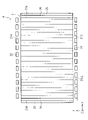
FIG. 1A shows a cross-sectional configuration example of a main part of the
表示装置1は、表示パネル10と、発光ユニット20と、ベゼル30と、スタンド40とを備えている。表示装置1では、表示パネル10と発光ユニット20とが対向配置され、それらの周縁部をベゼル30が覆うように構成されている。ここで、例えば表示パネル10、発光ユニット20およびベゼル30が、本開示の液晶モジュールに相当する一具体例である。スタンド40は、図2に示したように、表示パネル10、発光ユニット20およびベゼル30が一体となった表示部を床面上などに立設するものである。スタンド40は、例えば光源22(後述)を駆動する駆動回路やスピーカなどを搭載している。なお、本明細書では、表示パネル10の水平方向をX軸方向とし、表示パネル10の高さ方向をY軸方向とし、表示パネル10と発光ユニット20との積層方向をZ軸方向とする。 The
発光ユニット20は表示パネル10に照明光を提供する、いわゆるバックライトユニットである。発光ユニット20は、導光板21と、複数の光源22(図2)と、光学シート群23と、支持基板24と、保持部材25と、接着層26と、反射シート27と、光学膜28とを有している。 The
支持基板24は、表示パネル10の背面12(後出)と対向するように配置された、いわゆるバックシャーシであり、例えばステンレス鋼板やカラー鋼板などの高い剛性を有する金属材料を主たる構成材料とするものである。支持基板24は、背面12と対向する前面241と、その前面241と反対側の背面242とを有する。背面242の外縁近傍には、突出した爪部243が設けられている。 The
導光板21は、表示パネル10と支持基板24との間に設けられ、例えば対向する前面211および背面212と、それらを繋ぐ端面213~216とを含む平板状の部材である。なお、本実施の形態では、前面211および背面212が広がる面をXY平面とし、端面213および端面214が広がる面をXZ平面とし、一対の側面である端面215および端面216が広がる面をYZ平面としている。ここで、下面である端面213は光入射面として機能する。導光板21は、光源22からの光を表示パネル10へ導く部材である。具体的には、導光板21は、光源22から発せられたのち光入射面たる端面213に入射した光を内部において伝播させ、光出射面たる前面211から表示パネル10へ向けて出射するように機能する。導光板21の構成材料としては透明性の高い材料が好適であり、例えばガラスのほか、ポリメチルメタクリレート(Poly Methyl Methacrylate:PMMA)などのアクリル樹脂や、ポリカーボネート(PC)および環状ポリオレフィン(COP)などの他の樹脂材料が挙げられる。これらの構成材料のうち、特にガラスが好ましい。樹脂材料と比較して、温度変化に伴う寸法の変化(すなわち体積膨張率)が小さいうえ、高い剛性を有するからである。 The
なお、本実施の形態では、下面である端面213のみから光を入射するようにしたが、例えば上面である端面214から光を入射するようにしてもよい。あるいは、側面である端面215および端面216から光を入射するようにしてもよい。 In the present embodiment, the light is incident only from the
端面214~216は研磨処理などにより加工された鏡面であり、光学膜28により覆われている。光学膜28は、例えば光反射層として機能するものであり、反射インキなどを印刷、塗布または蒸着により端面214~216に付着させることにより得られる。また、光学膜28は光吸収層として機能するものとしてもよい。その場合、例えば黒色樹脂などの光吸収材料を印刷、塗布または蒸着等することにより光吸収層を形成するとよい。このような光学膜28を設けることにより、端面214~216に到達した光源22からの光が端面214~216から導光板21の外へ漏れたり、端面214~216において散乱したりするのを防ぐことができる。ただし、発光効率の観点から、光学膜28は、光吸収層よりも光反射層であることが望ましい。 The end faces 214 to 216 are mirror surfaces processed by polishing or the like, and are covered with an
なお、本実施の形態では、光学膜28と接着層26とをそれぞれ別体として設けるようにしたが、光学膜28および接着層26の機能を兼ね備えた接着テープにより構成してもよい。 In the present embodiment, the
複数の光源22はいずれも点光源であり、例えば白色光を発振する発光ダイオード(LED:Light Emitting Diode)により構成されている。複数の光源22は、導光板21における光入射面としての端面213と対向しており、X軸方向に並ぶように配置されている。1または2以上の光源22が1つの回路基板に載置されて1つの光源ユニットを構成するようにしてもよい。 Each of the plurality of
反射シート27は導光板21の背面212と対向するように設けられている。反射シート27は、導光板21の背面212から漏れる光源22からの光を反射させ、導光板21へ戻すように機能するものである。これにより、発光ユニット20の発光効率を高めることができる。反射シート27の構成材料としては、例えばポリカーボネート樹脂、PMMA(ポリメチルメタクリレート樹脂)などのアクリル樹脂、ポリエチレンテレフタレートなどのポリエステル樹脂、MS(メチルメタクリレートとスチレンの共重合体)などの非晶性共重合ポリエステル樹脂、ポリスチレン樹脂およびポリ塩化ビニル樹脂などが挙げられる。 The
保持部材25は、表示パネル10と支持基板24との間において支持基板24の外縁に沿って設けられている。保持部材25は、例えば導光板21の端面214と接合された対向面251を有している。保持部材25の対向面251と導光板21の端面214とは、接着層26を介して接合されている。接着層26の構成材料としては、例えば、十分な接着力および弾性を有する接着剤、具体的には、アクリル樹脂,ウレタン樹脂,エポキシ樹脂,塩化ビニル樹脂,変成シリコーン樹脂等の接着剤が挙げられる。さらに、保持部材25と支持基板24とが、例えばねじ29により互いに固定されている。保持部材25は、例えばアルミニウムやステンレス鋼などの金属材料により構成されるとよい。また、保持部材25は、支持基板24上の領域のうち、導光板21が占める中央領域以外の周辺領域に設けられている。また、保持部材25は、緩衝材51を介して表示パネル10を保持している。なお、図2では、導光板21の端面214と対向する位置にのみ保持部材25を設けるようにした例を記載したが、例えば端面215および端面216とそれぞれ対向する位置にも他の保持部材25を設けるようにしてもよい。 The holding
光学シート群23は、光源22から発せられたのち、導光板21を経由して表示パネル10へ向かう光に対して種々の光学的作用を付与するものである。光学シート群23は、例えば拡散板,拡散シート,レンズフィルム,偏光分離シートなどのシート状部材が複数積層されたものである。 The
表示パネル10は、動画像または静止画像などの画像を表示する透過型の液晶表示パネルであり、例えばTFT基板とカラーフィルタ基板との間に液晶層が設けられたものである。表示パネル10は、発光ユニット20からの光が入射することとなる背面12と、その光が出射することとなる前面11とを有している。表示パネル10は、さらに偏光板等を有していてもよい。 The
ベゼル30は、表示パネル10の周縁部および発光ユニット20の周縁部をそれぞれ保護すると共に審美性を向上させるための枠部材である。ベゼル30は、図2に示したように、例えば4つの部材30A~30Dに分割可能に構成されている。部材30A~30Dは、導光板21の端面213~216とそれぞれ対向するように設けられている。ただし、部材30Bと導光板21の端面214との間には、保持部材25が設けられている。さらに、部材30Cと端面215との間、および部材30Dと端面216との間にもそれぞれ保持部材25を設けるようにしてもよい。 The
各部材30A~30Dは、図1Aおよび図1Bに示したように、例えば厚さ方向(Z軸方向)に表示パネル10の周縁部および発光ユニット20の周縁部を挟み込むように設けられた前方部分31および後方部分32と、それら前方部分31と後方部分32とを繋ぐように設けられた側方部分33とを有している。各部材30A~30Dは、前方部分31、後方部分32および側方部分33を全て一体に成型したものであってもよい。または、各部材30A~30Dは、前方部分31、後方部分32および側方部分33を個別に成型したものを、ねじ留めや接着等により連結することにより構成されたものであってもよい。また、後方部分32は、支持基板24の爪部243と係合可能に設けられた凹部32Uを有しているとよい。その場合、凹部32Uが爪部243と係合することにより、ベゼル30が支持基板24の所定の位置に保持されることとなる。さらに、ベゼル30は支持基板24にねじ留めされ、または磁力により支持基板24に保持されるようになっているとよい。また、表示パネル10の前面とベゼル30の前方部分31との間には、発光ユニット20の周縁部からの漏れ光を遮蔽するための遮光シート52が設けられているとよい。遮光シート52は、表示パネル10とベゼル30とを安定的に保持するための緩衝材としても機能するよう、弾性を有するものであるとよい。 As shown in FIGS. 1A and 1B, the
[表示装置1の作用および効果]
このように、本実施の形態の表示装置1では、表示パネル10と支持基板24との間に挟まれた保持部材25が、その対向面251と導光板21の端面214との接合により、導光板21を保持するようになっている。よって、保持部材25が、例えば導光板21の端部を厚さ方向(Z軸方向)に挟持するような構造を有する場合と比較して、保持部材25の厚さが低減される。したがって、表示装置1によれば、薄型化に適した構造が実現できる。[Action and effect of display device 1]
As described above, in the
また、表示装置1では、導光板21をガラス材料により構成することで、さらなる薄型化が可能である。樹脂材料と比較してガラス材料は剛性が高いので、ガラス材料からなる導光板21が構造体としての機能を果たすからである。すなわち、樹脂材料ではなくガラス材料を用いることで導光板21の歪みや撓みが抑制され、表示パネル10と発光ユニット20との間隔(例えば背面12と光学シート群23の前面231との間隔)が狭小化できる。その結果、表示装置1全体としての薄型化が実現される。 Further, in the
また、導光板21をガラス材料により構成することで、いわゆる狭額縁化に有利となる。樹脂材料と比較してガラス材料は熱膨張率が低いので、ガラス材料からなる導光板21の温度変化に伴う膨張収縮が抑制できる。このため、例えば図1Aにおいて、ベゼル30の側方部分33の内面と保持部材25との隙間を縮小できる。結果としてY軸方向のベゼル30の寸法を縮小でき、表示装置1の狭額縁化が実現できる。 Further, by forming the
また、表示装置1では、保持部材25と支持基板24とをねじ29により締結し、ベゼル30を支持基板24の爪部243と係合することにより支持基板24に保持するようにしたので、高解体性が確保されている。 Further, in the
また、表示装置1では、導光板21をガラス材料により構成し、支持基板24を金属材料により構成することにより、発光ユニット20の高剛性化を実現することができる。 Further, in the
<2.第2の実施の形態>
[表示装置2の構成]
主に図3Aおよび図3Bを参照して、本開示の第2の実施の形態としての表示装置2について説明する。図3Aは、表示装置2の要部の断面構成例を表しており、図3Bは、表示装置2の内部構成例を表す部分破断斜視図である。表示装置2もまた、例えばテレビジョン装置として用いられる液晶表示装置である。表示装置2は、ベゼル30の代わりにベゼル60を設けるようにしたことを除き、他は上記第1の実施の形態の表示装置1と同じ構造を有する。<2. Second Embodiment>
[Configuration of display device 2]
The
表示装置1では、ベゼル30が、厚さ方向に表示パネル10および発光ユニット20を挟むように設けられた前方部分31および後方部分32を有するようにした。これに対し、表示装置2では、ベゼル60が厚さ方向において表示パネル10と発光ユニット20との間に挟まれた部分(第2部分62)を有するようにした。 In the
具体的には、ベゼル60は、表示パネル10の端面および発光ユニット20の端面の双方を覆う第1部分61と、その第1部分61に立設する第2部分62と、その第2部分62に立設する第3部分63とを有する。 Specifically, the
ここで、ベゼル60の第3部分63が支持基板24と、例えばねじにより固定されている。あるいは、第3部分63を永久磁石により構成し、支持基板24を第3部分63が磁力により引き付けるようにしてもよい。また、保持部材25は、ベゼル60の第3部分63と支持基板24との固定により、それらに挟持されている。 Here, the
この表示装置2においても、保持部材25が、その対向面251と導光板21の端面214との接合により、導光板21を保持するようになっている。よって、上記第1の実施の形態における表示装置1と同様の効果が期待できる。 Also in this
<3.変形例>
上記実施の形態では、光学膜28を、導光板21における端面213以外の端面214~216の全てに設けるようにしたが、本開示はそのような構成に限定されるものではない。例えば図4Aおよび図4Bに示した第1の変形例としての表示装置3では、前面211に、例えば、Y軸方向に伸びる微細な凸部(シリンドリカルレンズ)がX軸方向に複数並んでなるレンチキュラーレンズ21LLが設けられている。このようなレンチキュラーレンズ21LLの存在により、導光板21内を伝播する光の直進性を向上させることができる。この場合、光源22から発せられたのち端面213に入射した光は、おおよそ+Y方向へ直進することとなり、X軸方向への広がりが抑制される。このため、表示装置3では、端面215,216に到達する光成分が十分に低減されるので、端面213と対向する端面214のみに光学膜28を形成すれば足り、端面215,216には光学膜28を設けなくてすむ。<3. Modification example>
In the above embodiment, the
また、上記実施の形態では、導光板21の下部に位置する端面213と対向するように複数の光源22を配置したが、本開示はこれに限定されるものではない。例えば図5に示した第2の変形例としての表示装置4のように、例えば導光板21の端面213と対向する位置および端面214と対向する位置の双方に光源22を配置するようにしてもよい。この場合も、導光板21の前面211にレンチキュラーレンズ21LLを設けるようにし、導光板21へ入射する光のY軸方向への直進性を高めるようにすれば、端面215,216には光学膜28を設けなくてすむ。 Further, in the above embodiment, a plurality of
さらに、導光板21の背面212には、導光板21内を伝播する光を散乱し、均一化させる散乱部として、例えば、散乱剤が離散的に印刷されてなる散乱構造が形成されていてもよい。なお、そのような散乱構造は、散乱剤のパターン印刷に代えて、フィラーを含んだ部位を設けたものであってもよいし、表面を部分的に粗面化したものであってもよい。このような構成により、発光ユニット20の発光輝度分布のさらなる均質化が可能となる。 Further, on the
<4.照明装置への適用例>
図6は、上記実施の形態の発光ユニット20が適用される室内用の照明装置の外観を表したものである。この照明装置は、例えば、上記実施の形態に係る発光ユニット20により構成された照明部844を有している。照明部844は、建造物の天井850Aに適宜の個数および間隔で配置されている。なお、照明部844は、用途に応じて、天井850Aに限らず、壁850Bまたは床(図示せず)など任意の場所に設置することが可能である。<4. Application example to lighting equipment>
FIG. 6 shows the appearance of an indoor lighting device to which the
この照明装置では、発光ユニット20からの光により、照明が行われる。この照明装置は薄型化、挟額縁化および高剛性化された発光ユニット20を備えているので、省スペースへの設置が可能である。 In this lighting device, lighting is performed by the light from the
以上、いくつかの実施の形態および変形例を挙げて本開示を説明したが、本開示は上記実施の形態等に限定されるものではなく、種々の変形が可能である。例えば、上記実施の形態等において説明した保持部材、ベゼルおよび支持基板等の配置位置や形状などは一例であって、それらに限定されるものではない。 Although the present disclosure has been described above with reference to some embodiments and modifications, the present disclosure is not limited to the above embodiments and the like, and various modifications are possible. For example, the arrangement positions and shapes of the holding member, the bezel, the support substrate, and the like described in the above-described embodiment are merely examples, and the present invention is not limited thereto.
また、各図に示した各構成要素の寸法および寸法比や形状は一例であって本開示がこれに限定されるものではない。 Further, the dimensions, dimensional ratios and shapes of each component shown in each figure are examples, and the present disclosure is not limited thereto.
また、上記実施の形態等では、光源22としてLEDを用いるようにしたが、光源22として半導体レーザ等を用いるようにしてもよい。 Further, in the above-described embodiment or the like, the LED is used as the
さらに、例えば、上記実施の形態等に記載した表示装置は、説明した全ての構成要素を備えた場合に限定されるものではなく、いくつかの構成要素を欠いてもよいし、他の構成要素をさらに備えていてもよい。 Further, for example, the display device described in the above-described embodiment is not limited to the case where all the components described above are provided, and some components may be omitted or other components may be omitted. May be further provided.
例えば、上記実施の形態等で説明した表示装置1,2は、発光ユニット20の支持基板24の、表示パネル10と反対側に配置されるリアカバーをさらに備えるようにしてもよい。リアカバーは、例えばポリスチレン(PS:polystyrene)、ポリスチレンとポリフェニレンエーテル(PPE:polyphenyleneether)との混合材料等により構成される。表示装置1,2は、さらに他の化粧部材を備えるようにしてもよい。また、支持基板24は、アルミニウムにより構成されてもよい。また、支持基板24の背面242に、発光ユニット20を駆動する駆動回路を含む基板やチューナーを搭載するようにしてもよい。 For example, the
また、上記実施の形態等で説明した表示装置1,2は、家庭内で使用されるテレビジョンに限定されるものではなく、広く屋内外で情報表示を行うものも含まれる。さらには、各種医療機器(例えば内視鏡手術システム、手術室システムあるいは顕微鏡手術システムなど)への適用可能性を有する。 Further, the
なお、本明細書中に記載された効果はあくまで例示であってその記載に限定されるものではなく、他の効果があってもよい。また、本技術は以下のような構成を取り得るものである。
(1)
表示パネルと、前記表示パネルを照明する発光ユニットとを有する液晶モジュールを備え、
前記発光ユニットは、
前記表示パネルと対向配置された支持基板と、
前記表示パネルと前記支持基板との間に設けられ、第1の端面および第2の端面を含む導光部材と、
前記第1の端面と対向するように配置された光源と、
前記表示パネルと前記支持基板との間において前記支持基板の外縁に沿って設けられ、前記第2の端面と接合された対向面を含む保持部材と
を有する
表示装置。
(2)
前記第2の端面は鏡面であり、光反射層または光吸収層により覆われている
上記(1)記載の表示装置。
(3)
前記第2の端面と前記対向面とは接着部材により接合されている
上記(1)または(2)に記載の表示装置。
(4)
前記支持基板は金属材料からなり、
前記導光部材はガラス材料からなり、
前記保持部材は金属材料からなる
上記(1)から(3)のいずれか1つに記載の表示装置。
(5)
前記支持基板と前記保持部材とを固定するねじをさらに備える
上記(4)に記載の表示装置。
(6)
前記保持部材は、前記支持基板の上の、前記導光部材が占める中央領域以外の周辺領域に設けられている
上記(1)から(5)のいずれか1つに記載の表示装置。
(7)
枠部材をさらに備え、
前記枠部材は前記支持基板にねじ留めされ、または前記枠部材は磁力により前記支持基板に保持されている
上記(1)から(6)のいずれか1つに記載の表示装置。
(8)
支持基板と、
前記支持基板と対向するように配置され、第1の端面および第2の端面を含む導光部材と、
前記第1の端面と対向するように配置された光源と、
前記支持基板の外縁に沿って設けられ、前記第2の端面と接合された対向面を含む保持部材と
を有する
発光ユニット。
(9)
発光ユニットを備え、
前記発光ユニットは、
支持基板と、
前記支持基板と対向するように配置され、第1の端面および第2の端面を含む導光部材と、
前記第1の端面と対向するように配置された光源と、
前記支持基板の外縁に沿って設けられ、前記第2の端面と接合された対向面を含む保持部材と
を有する
照明装置。
(10)
表示パネルと、
前記表示パネルを照明する発光ユニットと
を備え、
前記発光ユニットは、
前記表示パネルと対向配置された支持基板と、
前記表示パネルと前記支持基板との間に設けられ、第1の端面および第2の端面を含む導光部材と、
前記第1の端面と対向するように配置された光源と、
前記表示パネルと前記支持基板との間において前記支持基板の外縁に沿って設けられ、前記第2の端面と接合された対向面を含む保持部材と
を有する
液晶モジュール。It should be noted that the effects described in the present specification are merely examples and are not limited to the description thereof, and other effects may be obtained. In addition, the present technology can have the following configurations.
(1)
A liquid crystal module having a display panel and a light emitting unit for illuminating the display panel is provided.
The light emitting unit is
A support board arranged to face the display panel and
A light guide member provided between the display panel and the support substrate and including a first end face and a second end face,
A light source arranged so as to face the first end face,
A display device having a holding member provided between the display panel and the support substrate along the outer edge of the support substrate and including a facing surface joined to the second end surface.
(2)
The display device according to (1) above, wherein the second end surface is a mirror surface and is covered with a light reflecting layer or a light absorbing layer.
(3)
The display device according to (1) or (2) above, wherein the second end surface and the facing surface are joined by an adhesive member.
(4)
The support substrate is made of a metal material and is made of a metal material.
The light guide member is made of glass material.
The display device according to any one of (1) to (3) above, wherein the holding member is made of a metal material.
(5)
The display device according to (4) above, further comprising a screw for fixing the support substrate and the holding member.
(6)
The display device according to any one of (1) to (5) above, wherein the holding member is provided on a support substrate in a peripheral region other than the central region occupied by the light guide member.
(7)
With more frame members
The display device according to any one of (1) to (6) above, wherein the frame member is screwed to the support substrate, or the frame member is held by the support substrate by a magnetic force.
(8)
Support board and
A light guide member arranged so as to face the support substrate and including a first end face and a second end face,
A light source arranged so as to face the first end face,
A light emitting unit provided along the outer edge of the support substrate and having a holding member including a facing surface joined to the second end surface.
(9)
Equipped with a light emitting unit
The light emitting unit is
Support board and
A light guide member arranged so as to face the support substrate and including a first end face and a second end face,
A light source arranged so as to face the first end face,
A lighting device provided along the outer edge of the support substrate and having a holding member including a facing surface joined to the second end surface.
(10)
Display panel and
It is equipped with a light emitting unit that illuminates the display panel.
The light emitting unit is
A support board arranged to face the display panel and
A light guide member provided between the display panel and the support substrate and including a first end face and a second end face,
A light source arranged so as to face the first end face,
A liquid crystal module having a holding member provided between the display panel and the support substrate along the outer edge of the support substrate and including a facing surface joined to the second end surface.
本出願は、日本国特許庁において2016年5月25日に出願された日本特許出願番号2016-104062号を基礎として優先権を主張するものであり、この出願のすべての内容を参照によって本出願に援用する。 This application claims priority on the basis of Japanese Patent Application No. 2016-104062 filed at the Japan Patent Office on May 25, 2016, and this application is made by reference to all the contents of this application. Invite to.
当業者であれば、設計上の要件や他の要因に応じて、種々の修正、コンビネーション、サブコンビネーション、および変更を想到し得るが、それらは添付の請求の範囲やその均等物の範囲に含まれるものであることが理解される。 Those skilled in the art may conceive various modifications, combinations, sub-combinations, and changes, depending on design requirements and other factors, which are included in the claims and their equivalents. It is understood that it is a person skilled in the art.
Claims (8)
前記発光ユニットは、
前記表示パネルと対向配置された支持基板と、
前記表示パネルと前記支持基板との間に設けられ、第1の端面および第2の端面を含む導光部材と、
前記第1の端面と対向するように配置された光源と、
前記表示パネルと前記支持基板との間において前記支持基板の外縁に沿って設けられ、前記第2の端面と接合された対向面を含む保持部材と
を有し、
前記遮光シートは、前記枠部材と、前記表示パネルのうち前記発光ユニットとは反対側の面との間に設けられ、弾性を有する
表示装置。 A display panel, a light emitting unit facing the display panel in the first direction and illuminating the display panel, a frame member sandwiching a peripheral portion of the display panel and a peripheral edge of the light emitting unit, and a light-shielding sheet are provided. ,
The light emitting unit is
A support board arranged to face the display panel and
A light guide member provided between the display panel and the support substrate and including a first end face and a second end face,
A light source arranged so as to face the first end face,
It has a holding member provided between the display panel and the support substrate along the outer edge of the support substrate and includes a facing surface joined to the second end surface.
The light-shielding sheet is provided between the frame member and the surface of the display panel on the side opposite to the light-emitting unit, and has elasticity.
Display device.
請求項1記載の表示装置。 The display device according to claim 1, wherein the second end surface is a mirror surface and is covered with a light reflecting layer or a light absorbing layer.
請求項1記載の表示装置。 The display device according to claim 1, wherein the second end surface and the facing surface are joined by an adhesive member.
前記導光部材はガラス材料からなり、
前記保持部材は金属材料からなる
請求項1記載の表示装置。 The support substrate is made of a metal material and is made of a metal material.
The light guide member is made of glass material.
The display device according to claim 1, wherein the holding member is made of a metal material.
請求項4記載の表示装置。 The display device according to claim 4, further comprising a screw for fixing the support substrate and the holding member.
請求項1記載の表示装置。 The display device according to claim 1, wherein the holding member is provided on a support substrate in a peripheral region other than the central region occupied by the light guide member.
請求項1記載の表示装置。 The display device according to claim 1, wherein the frame member is screwed to the support substrate, or the frame member is held on the support substrate by a magnetic force.
請求項1から請求項7のいずれか1項に記載の表示装置。 The display device according to any one of claims 1 to 7, wherein the holding member has a thickness equal to or less than the thickness of the light guide member in the first direction.
Priority Applications (1)
| Application Number | Priority Date | Filing Date | Title |
|---|---|---|---|
| JP2021081047A JP7150093B2 (en) | 2016-05-25 | 2021-05-12 | Display device and liquid crystal module |
Applications Claiming Priority (3)
| Application Number | Priority Date | Filing Date | Title |
|---|---|---|---|
| JP2016104062 | 2016-05-25 | ||
| JP2016104062 | 2016-05-25 | ||
| PCT/JP2017/011629 WO2017203816A1 (en) | 2016-05-25 | 2017-03-23 | Light emitting unit, liquid crystal module, display device, and illuminating device |
Related Child Applications (1)
| Application Number | Title | Priority Date | Filing Date |
|---|---|---|---|
| JP2021081047A Division JP7150093B2 (en) | 2016-05-25 | 2021-05-12 | Display device and liquid crystal module |
Publications (2)
| Publication Number | Publication Date |
|---|---|
| JPWO2017203816A1 JPWO2017203816A1 (en) | 2019-03-22 |
| JP7085472B2 true JP7085472B2 (en) | 2022-06-16 |
Family
ID=60412164
Family Applications (2)
| Application Number | Title | Priority Date | Filing Date |
|---|---|---|---|
| JP2018519113A Active JP7085472B2 (en) | 2016-05-25 | 2017-03-23 | Light emitting unit, liquid crystal module, display device and lighting device |
| JP2021081047A Active JP7150093B2 (en) | 2016-05-25 | 2021-05-12 | Display device and liquid crystal module |
Family Applications After (1)
| Application Number | Title | Priority Date | Filing Date |
|---|---|---|---|
| JP2021081047A Active JP7150093B2 (en) | 2016-05-25 | 2021-05-12 | Display device and liquid crystal module |
Country Status (5)
| Country | Link |
|---|---|
| US (3) | US11460630B2 (en) |
| EP (1) | EP3467580A4 (en) |
| JP (2) | JP7085472B2 (en) |
| CN (1) | CN109154744B (en) |
| WO (1) | WO2017203816A1 (en) |
Families Citing this family (3)
| Publication number | Priority date | Publication date | Assignee | Title |
|---|---|---|---|---|
| WO2017203816A1 (en) * | 2016-05-25 | 2017-11-30 | ソニー株式会社 | Light emitting unit, liquid crystal module, display device, and illuminating device |
| US10571690B2 (en) * | 2018-06-29 | 2020-02-25 | GM Global Technology Operations LLC | Automotive window with transparent light guide display |
| CN108957620B (en) * | 2018-08-01 | 2020-07-07 | 京东方科技集团股份有限公司 | Light guide plate, preparation method of light guide plate, backlight module and display device |
Citations (3)
| Publication number | Priority date | Publication date | Assignee | Title |
|---|---|---|---|---|
| JP2015176752A (en) | 2014-03-14 | 2015-10-05 | 日本精機株式会社 | Lighting device and display device |
| WO2016031397A1 (en) | 2014-08-28 | 2016-03-03 | ソニー株式会社 | Display device and lighting device |
| WO2016031394A1 (en) | 2014-08-28 | 2016-03-03 | ソニー株式会社 | Display device |
Family Cites Families (29)
| Publication number | Priority date | Publication date | Assignee | Title |
|---|---|---|---|---|
| JPH08190085A (en) * | 1995-01-09 | 1996-07-23 | Citizen Watch Co Ltd | Liquid crystal display device |
| JP4923490B2 (en) * | 2005-09-06 | 2012-04-25 | カシオ計算機株式会社 | Display device |
| JP2006108116A (en) * | 2005-12-07 | 2006-04-20 | Enplas Corp | Surface light source device and image display device |
| JP2007163620A (en) * | 2005-12-12 | 2007-06-28 | Hitachi Displays Ltd | Liquid crystal display device and backlight device |
| JP5098549B2 (en) * | 2007-10-04 | 2012-12-12 | 船井電機株式会社 | LCD module |
| KR100893619B1 (en) * | 2008-02-18 | 2009-04-20 | 삼성모바일디스플레이주식회사 | Electronic device having organic light emitting display |
| KR101607572B1 (en) | 2009-10-12 | 2016-03-31 | 삼성디스플레이 주식회사 | Back-light assembly and display device having the same |
| KR101354223B1 (en) * | 2009-12-14 | 2014-01-22 | 엘지디스플레이 주식회사 | Liquid crystal display device |
| JP2012208254A (en) * | 2011-03-29 | 2012-10-25 | Funai Electric Co Ltd | Illumination device for display device and display device |
| JP5892736B2 (en) * | 2011-05-24 | 2016-03-23 | ソニー株式会社 | Display device |
| JP2013008016A (en) * | 2011-05-24 | 2013-01-10 | Sony Corp | Display unit |
| KR20130034470A (en) * | 2011-09-28 | 2013-04-05 | 삼성디스플레이 주식회사 | Back-light unit and display device having the same |
| KR101347566B1 (en) | 2012-05-01 | 2014-01-06 | 엘지디스플레이 주식회사 | Display apparatus and method for manufacturing the same |
| KR101952774B1 (en) * | 2012-05-17 | 2019-02-27 | 엘지디스플레이 주식회사 | Back light unit and liquid crystal display device comprising the same |
| TWI522690B (en) | 2012-07-26 | 2016-02-21 | 揚昇照明股份有限公司 | Hybrid light guide plate and display device |
| WO2014034487A1 (en) * | 2012-08-28 | 2014-03-06 | シャープ株式会社 | Lighting apparatus, display apparatus, and television receiver |
| JP5519758B2 (en) | 2012-11-09 | 2014-06-11 | シャープ株式会社 | Liquid crystal display |
| KR20150027969A (en) * | 2013-09-05 | 2015-03-13 | 삼성디스플레이 주식회사 | Liquid Crystal Display device united Touch Screen Panel |
| US10042110B2 (en) | 2014-07-21 | 2018-08-07 | Samsung Display Co., Ltd. | Liquid crystal display and manufacturing method thereof |
| WO2016046973A1 (en) | 2014-09-26 | 2016-03-31 | 堺ディスプレイプロダクト株式会社 | Display device |
| CN104267524A (en) * | 2014-10-20 | 2015-01-07 | 京东方科技集团股份有限公司 | Backlight module and display device |
| CN104819440B (en) * | 2015-05-07 | 2017-12-05 | 武汉华星光电技术有限公司 | Light guide plate and preparation method thereof, backlight module |
| CN104914624A (en) * | 2015-06-19 | 2015-09-16 | 京东方科技集团股份有限公司 | Light guide structure, backlight module and display device |
| CN105044981B (en) * | 2015-08-10 | 2018-03-02 | 武汉华星光电技术有限公司 | A kind of backlight module and liquid crystal display device |
| CN105278030A (en) * | 2015-10-20 | 2016-01-27 | 深圳市华星光电技术有限公司 | Backlight module and liquid crystal display |
| CN105384337A (en) * | 2015-11-04 | 2016-03-09 | 芜湖东旭光电装备技术有限公司 | Glass, light guide plate, backlight unit, liquid crystal panel, liquid crystal display terminal and preparation method of glass |
| CN205193310U (en) * | 2015-11-06 | 2016-04-27 | 乐视致新电子科技(天津)有限公司 | Leaded light module reaches display device including leaded light module |
| CN105549265B (en) * | 2016-03-03 | 2018-11-09 | 武汉华星光电技术有限公司 | A kind of backlight module and liquid crystal display |
| WO2017203816A1 (en) * | 2016-05-25 | 2017-11-30 | ソニー株式会社 | Light emitting unit, liquid crystal module, display device, and illuminating device |
-
2017
- 2017-03-23 WO PCT/JP2017/011629 patent/WO2017203816A1/en unknown
- 2017-03-23 JP JP2018519113A patent/JP7085472B2/en active Active
- 2017-03-23 CN CN201780030082.6A patent/CN109154744B/en active Active
- 2017-03-23 US US16/096,067 patent/US11460630B2/en active Active
- 2017-03-23 EP EP17802418.8A patent/EP3467580A4/en active Pending
-
2021
- 2021-05-12 JP JP2021081047A patent/JP7150093B2/en active Active
-
2022
- 2022-08-09 US US17/883,657 patent/US11726255B2/en active Active
-
2023
- 2023-06-27 US US18/214,730 patent/US20230408753A1/en active Pending
Patent Citations (3)
| Publication number | Priority date | Publication date | Assignee | Title |
|---|---|---|---|---|
| JP2015176752A (en) | 2014-03-14 | 2015-10-05 | 日本精機株式会社 | Lighting device and display device |
| WO2016031397A1 (en) | 2014-08-28 | 2016-03-03 | ソニー株式会社 | Display device and lighting device |
| WO2016031394A1 (en) | 2014-08-28 | 2016-03-03 | ソニー株式会社 | Display device |
Also Published As
| Publication number | Publication date |
|---|---|
| US20190129091A1 (en) | 2019-05-02 |
| CN109154744A (en) | 2019-01-04 |
| US11726255B2 (en) | 2023-08-15 |
| WO2017203816A1 (en) | 2017-11-30 |
| US20230408753A1 (en) | 2023-12-21 |
| JP7150093B2 (en) | 2022-10-07 |
| JP2021122020A (en) | 2021-08-26 |
| US11460630B2 (en) | 2022-10-04 |
| EP3467580A4 (en) | 2019-05-15 |
| CN109154744B (en) | 2023-03-10 |
| JPWO2017203816A1 (en) | 2019-03-22 |
| US20220390667A1 (en) | 2022-12-08 |
| EP3467580A1 (en) | 2019-04-10 |
Similar Documents
| Publication | Publication Date | Title |
|---|---|---|
| JP7150093B2 (en) | Display device and liquid crystal module | |
| US7576976B2 (en) | Display device | |
| JP6991373B2 (en) | Light emitting device, display device and lighting device | |
| JP2013218953A (en) | Light-emitting device, display device and lighting device | |
| JP2022000857A (en) | Light-emitting device, display device, and lighting device | |
| JP2019185921A (en) | Illuminating device and display device comprising the same | |
| JP6567576B2 (en) | Display device | |
| WO2017068845A1 (en) | Light-emission device, display device, and illumination device | |
| JP2022031473A (en) | Display device | |
| JP7249779B2 (en) | Displays and electronics | |
| US20210109260A1 (en) | Optical Member, Light-Emitting Device, Display, And Illuminator | |
| JP7097812B2 (en) | Display device | |
| WO2018037892A1 (en) | Light-emitting device, display device, and illumination device | |
| WO2017073175A1 (en) | Light emitting device, display apparatus, and illumination apparatus | |
| WO2017064919A1 (en) | Light emission device, display device, and illumination device | |
| JP2020009661A (en) | Surface light source device and display device | |
| JP2015128011A (en) | Light emitting unit, light emitting device, display device and illumination device |
Legal Events
| Date | Code | Title | Description |
|---|---|---|---|
| A621 | Written request for application examination |
Free format text: JAPANESE INTERMEDIATE CODE: A621 Effective date: 20200213 |
|
| A131 | Notification of reasons for refusal |
Free format text: JAPANESE INTERMEDIATE CODE: A131 Effective date: 20200929 |
|
| A521 | Request for written amendment filed |
Free format text: JAPANESE INTERMEDIATE CODE: A523 Effective date: 20201117 |
|
| A02 | Decision of refusal |
Free format text: JAPANESE INTERMEDIATE CODE: A02 Effective date: 20210216 |
|
| A521 | Request for written amendment filed |
Free format text: JAPANESE INTERMEDIATE CODE: A523 Effective date: 20210512 |
|
| C60 | Trial request (containing other claim documents, opposition documents) |
Free format text: JAPANESE INTERMEDIATE CODE: C60 Effective date: 20210512 |
|
| A911 | Transfer to examiner for re-examination before appeal (zenchi) |
Free format text: JAPANESE INTERMEDIATE CODE: A911 Effective date: 20210527 |
|
| C21 | Notice of transfer of a case for reconsideration by examiners before appeal proceedings |
Free format text: JAPANESE INTERMEDIATE CODE: C21 Effective date: 20210601 |
|
| A912 | Re-examination (zenchi) completed and case transferred to appeal board |
Free format text: JAPANESE INTERMEDIATE CODE: A912 Effective date: 20210827 |
|
| C211 | Notice of termination of reconsideration by examiners before appeal proceedings |
Free format text: JAPANESE INTERMEDIATE CODE: C211 Effective date: 20210831 |
|
| C22 | Notice of designation (change) of administrative judge |
Free format text: JAPANESE INTERMEDIATE CODE: C22 Effective date: 20211109 |
|
| C13 | Notice of reasons for refusal |
Free format text: JAPANESE INTERMEDIATE CODE: C13 Effective date: 20220111 |
|
| A521 | Request for written amendment filed |
Free format text: JAPANESE INTERMEDIATE CODE: A523 Effective date: 20220310 |
|
| C23 | Notice of termination of proceedings |
Free format text: JAPANESE INTERMEDIATE CODE: C23 Effective date: 20220405 |
|
| C22 | Notice of designation (change) of administrative judge |
Free format text: JAPANESE INTERMEDIATE CODE: C22 Effective date: 20220412 |
|
| C03 | Trial/appeal decision taken |
Free format text: JAPANESE INTERMEDIATE CODE: C03 Effective date: 20220510 |
|
| C30A | Notification sent |
Free format text: JAPANESE INTERMEDIATE CODE: C3012 Effective date: 20220510 |
|
| A61 | First payment of annual fees (during grant procedure) |
Free format text: JAPANESE INTERMEDIATE CODE: A61 Effective date: 20220606 |
|
| R150 | Certificate of patent or registration of utility model |
Ref document number: 7085472 Country of ref document: JP Free format text: JAPANESE INTERMEDIATE CODE: R150 |