JP7083683B2 - Liquid crystal display device - Google Patents
Liquid crystal display device Download PDFInfo
- Publication number
- JP7083683B2 JP7083683B2 JP2018077772A JP2018077772A JP7083683B2 JP 7083683 B2 JP7083683 B2 JP 7083683B2 JP 2018077772 A JP2018077772 A JP 2018077772A JP 2018077772 A JP2018077772 A JP 2018077772A JP 7083683 B2 JP7083683 B2 JP 7083683B2
- Authority
- JP
- Japan
- Prior art keywords
- liquid crystal
- wiring board
- crystal display
- display device
- double
- Prior art date
- Legal status (The legal status is an assumption and is not a legal conclusion. Google has not performed a legal analysis and makes no representation as to the accuracy of the status listed.)
- Active
Links
Images


Description
本発明の実施形態は、液晶表示装置に関する。 Embodiments of the present invention relate to a liquid crystal display device.
近年、スマートフォン、タブレットコンピュータ、カーナビゲーションシステム等の表示装置として、液晶表示装置が広く用いられている。一般に、液晶表示装置は、液晶パネルと、この液晶パネルの背面に重ねて配置され液晶パネルを照明するバックライト装置と、を備えている。バックライト装置は、反射層、導光板、光学シート、光源ユニット、これらを収容する収容ケース(ベゼル)等を有している。光源ユニットは、配線基板と、この配線基板上に実装された複数の光源、例えば、発光ダイオード(LED)と、を有している。 In recent years, liquid crystal displays have been widely used as display devices for smartphones, tablet computers, car navigation systems, and the like. Generally, a liquid crystal display device includes a liquid crystal panel and a backlight device that is arranged on the back surface of the liquid crystal panel and illuminates the liquid crystal panel. The backlight device includes a reflective layer, a light guide plate, an optical sheet, a light source unit, a storage case (bezel) for accommodating these, and the like. The light source unit has a wiring board and a plurality of light sources mounted on the wiring board, for example, a light emitting diode (LED).
ところで、光源ユニットの配線基板は、収容ケースの背面側に折り込まれ、そこで中継プリント回路基板に電気的に接続される。この際、ハンダを用いて配線基板を中継プリント回路基板に電気的かつ機械的に接続するものがある。しかしながら、ハンダにより接合する場合、ハンダ付部は比較的大きな高さを有するハンダバンプを形成する。これらのハンダバンプは、バックライト装置および液晶表示装置を薄型化する上で、障害と成り得る。
ここで述べる実施形態の目的は、狭額縁化および薄型化が可能な液晶表示装置を提供することにある。
By the way, the wiring board of the light source unit is folded into the back side of the housing case, and is electrically connected to the relay printed circuit board there. At this time, there is a case where the wiring board is electrically and mechanically connected to the relay printed circuit board by using solder. However, when joined by soldering, the soldered portion forms a solder bump with a relatively large height. These solder bumps can be an obstacle in reducing the thickness of the backlight device and the liquid crystal display device.
An object of the embodiment described here is to provide a liquid crystal display device capable of narrowing the frame and making it thinner.
実施形態に係る液晶表示装置は、第1基板と、この第1基板に対向して配置された第2基板と、前記第1基板と第2基板との間に設けられた液晶層と、を有する液晶パネルと、前記第1基板に対向して設けられたバックライト装置と、を備えている。前記バックライト装置は、底板および底板の側縁に沿って立設された側板を備えるケースと、出射面と前記出射面に交差して延びる入射面とを有し、前記底板上に配置された導光板と、前記導光板の入射面に光を入射する光源ユニットと、を備えている。前記光源ユニットは、複数の配線を有する配線基板と、前記配線基板に実装された発光素子と、を有し、前記発光素子は、前記導光板の入射面に対向する発光面と、前記発光面の反対側に位置し前記配線基板に実装される実装面と、を有している。前記配線基板は、前記発光素子が実装されているとともに前記発光素子を挟んで前記入射面と対向する実装部と、前記底板の背面側に配置される接続配線部と、前記実装部と前記接続配線部とを連結している連結部と、を一体に備えている。前記ケースの側板と前記液晶パネルとの間にギャップが設けられ、前記ギャップを通じて前記配線基板の連結部が前記側板の端縁を回り込んだ状態で前記側板の端縁および前記側板の外面に沿って前記ケースの内側から外側に延在している。前記側板の内面と前記実装部との間、前記側板の端縁と前記連結部との間、および前記側板の外面と前記連結部との間、に両面テープが設けられている。 The liquid crystal display device according to the embodiment includes a first substrate, a second substrate arranged to face the first substrate, and a liquid crystal layer provided between the first substrate and the second substrate. It includes a liquid crystal panel having a liquid crystal panel and a backlight device provided so as to face the first substrate. The backlight device has a bottom plate and a case including a side plate erected along the side edge of the bottom plate, and an exit surface and an incident surface extending so as to intersect the exit surface, and are arranged on the bottom plate. It includes a light guide plate and a light source unit that incidents light on the incident surface of the light guide plate. The light source unit includes a wiring board having a plurality of wirings and a light emitting element mounted on the wiring board, and the light emitting element has a light emitting surface facing an incident surface of the light guide plate and the light emitting surface. It has a mounting surface, which is located on the opposite side of the wiring board and is mounted on the wiring board. The wiring board includes a mounting portion on which the light emitting element is mounted and facing the incident surface across the light emitting element, a connection wiring portion arranged on the back surface side of the bottom plate, and the mounting portion and the connection. It is integrally provided with a connecting portion that connects the wiring portion. A gap is provided between the side plate of the case and the liquid crystal panel, and the connecting portion of the wiring board wraps around the edge of the side plate through the gap and is along the edge of the side plate and the outer surface of the side plate. It extends from the inside to the outside of the case. Double-sided tape is provided between the inner surface of the side plate and the mounting portion, between the edge of the side plate and the connecting portion, and between the outer surface of the side plate and the connecting portion.
以下、図面を参照しながら、この発明の実施形態について詳細に説明する。
なお、開示はあくまで一例にすぎず、当業者において、発明の主旨を保っての適宜変更であって容易に想到し得るものについては、当然に本発明の範囲に含有されるものである。また、図面は説明をより明確にするため、実際の態様に比べ、各部の幅、厚さ、形状等について模式的に表される場合があるが、あくまで一例であって、本発明の解釈を限定するものではない。また、本明細書と各図において、既出の図に関して前述したものと同様の要素には、同一の符号を付して、詳細な説明を適宜省略することがある。
Hereinafter, embodiments of the present invention will be described in detail with reference to the drawings.
It should be noted that the disclosure is merely an example, and those skilled in the art who are appropriately modified while maintaining the gist of the invention and which can be easily conceived are naturally included in the scope of the present invention. Further, in order to clarify the explanation, the drawings may schematically represent the width, thickness, shape, etc. of each part as compared with the actual embodiment, but this is just an example, and the interpretation of the present invention is used. It is not limited. Further, in the present specification and each figure, the same elements as those described above with respect to the above-mentioned figures may be designated by the same reference numerals, and detailed description thereof may be omitted as appropriate.
(実施形態)
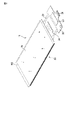
図1および図2は、実施形態に係る液晶表示装置の表示面側および背面側をそれぞれ示す斜視図、図3は、ドライバICが実装されたメインFPCを背面側に折り重ねた状態における液晶表示装置の背面側を示す斜視図、図4は、液晶表示装置の分解斜視図である。
液晶表示装置10は、例えばスマートフォン、タブレット端末、携帯電話機、ノートブックタイプPC、携帯型ゲーム機、電子辞書、テレビ装置、カーナビゲーションシステムなどの各種の電子機器に組み込んで使用することができる。
(Embodiment)
1 and 2 are perspective views showing the display surface side and the back surface side of the liquid crystal display device according to the embodiment, respectively, and FIG. 3 is a liquid crystal display in a state where the main FPC on which the driver IC is mounted is folded back side. A perspective view showing the back side of the device, FIG. 4 is an exploded perspective view of the liquid crystal display device.
The liquid
図1、図2、図4に示すように、液晶表示装置10は、アクティブマトリクス型の平板状の液晶パネル12と、液晶パネル12の一方の平板面である表示面12aに重ねて配置され、この表示面12a全体を覆う透明なカバーパネル14と、液晶パネル12の他方の平板面である背面に対向して配置されたバックライト装置としてのバックライトユニット20と、を備えている。
As shown in FIGS. 1, 2, and 4, the liquid
液晶パネル12は、矩形平板状の第1基板SUB1と、第1基板SUB1に対向配置された矩形平板状の第2基板SUB2と、第1基板SUB1と第2基板SUB2との間に保持された液晶層LQと、を備えている。第2基板SUB2の周縁部は、シール材SEにより第1基板SUB1に貼り合わされている。第2基板SUB2の表面に偏光板PL2が貼付され、液晶パネル12の表示面12aを形成している。第1基板SUB1の表面(液晶パネル12の背面)に偏光板PL1が貼付されている。
The
液晶パネル12は、平面視(液晶パネルの表示面の法線方向から当該液晶パネルを視認する状態をいう。以下同様。)でシール材SEの内側となる領域に矩形状の表示領域(アクティブ領域)DAが設けられ、該表示領域DAに画像が表示される。表示領域DAの周囲に、矩形枠状の額縁領域EDが設けられている。液晶パネル12は、バックライトユニット20からの光を表示領域DAに選択的に透過又は変調することで画像を表示する透過表示機能を備えた透過型の液晶パネルである。液晶パネル12は、主として基板主面に沿った横電界を利用する横電界モードに対応した構成を有していても良いし、主として基板主面に交差する縦電界を利用する縦電界モードに対応した構成を有していても良い。
The
図示した例では、第1基板SUB1の短辺側の端部にフレキシブルプリント回路基板(メインFPC)23が接合され、液晶パネル12から外方に延出している。メインFPC23には、液晶パネル12を駆動するのに必要な信号を供給する信号供給源として、ドライバIC24等の半導体素子が実装されている(かかるFPCにドライバICを実装した構成物をCOF(Chip On Flexible printed circuit)と称することがある)。メインFPC23の延出端に、サブFPC25が接合されている。このサブFPC25上に、コンデンサC1、コネクタ26、27等が実装されている。図3に示すように、メインFPC23およびサブFPC25は、第1基板SUB1の短辺側端縁に沿って折り返され、バックライトユニット20の底板に重ねて配置される。後述するように、メインFPC23およびサブFPC25は、両面テープ等の粘着部材により、バックライトユニット20の底板に貼付される。
In the illustrated example, the flexible printed circuit board (main FPC) 23 is bonded to the short side end of the first substrate SUB1 and extends outward from the
図1および図4に示すように、カバーパネル14は、例えば、ガラス板あるいはアクリル系の透明樹脂等により、矩形平板状に形成されている。カバーパネル14の下面(裏面、液晶パネル側の面)に枠状の遮光層RSが形成されている。カバーパネル14において、液晶パネル12の表示領域DAと対向する領域以外の領域は、遮光層RSにより遮光されている。遮光層RSは、カバーパネル14の上面(外面)に形成してもよい。なお、カバーパネル14は、液晶表示装置10の使用状況に応じて、省略してもよい。
As shown in FIGS. 1 and 4, the
バックライトユニット20は、偏平な矩形状の収容ケース22と、この収容ケース22内に敷設あるいは配置された光学部材および光源ユニット50と、を備えている。バックライトユニット20は、枠状の粘着部材、例えば、両面テープTP1により液晶パネル12の背面、例えば、偏光板PL1に貼付されている。
The
図4に示すように、液晶パネル12は、各辺の非表示領域EDの幅がいずれも同じか、或いは略同じとなっている。より具体的には、表示領域DAの一対の長辺に対する非表示領域EDの幅WL1、WL2は、互いに等しい大きさとなっている(WL1=WL2)。ここで、非表示領域の幅WL1、WL2とは、具体的には、当該表示領域DAの長辺において、表示領域DAと非表示領域EDの境界から第1基板SUB1(及び第2基板SUB2)の外縁までの大きさのことを示している。また、表示領域DAの一対の短辺のうち、フレキシブルプリント回路基板23が設けられる側(以下、実装側とも称する)の非表示領域EDの幅をWS1、これとは反対側となる短辺側の非表示領域EDの幅をWS2とすると、WS2≦WS1であって且つ、WS1/WS2≦2.0となることが好ましく、より好ましくWS1/WS2≦1.5、さらに好ましくはWS1/WS2≦1.0を採用することができる。ここで、非表示領域の幅WS1とは、当該表示領域DAの実装側の短辺において、表示領域DAと非表示領域EDの境界から第2基板SUB2の外縁までの大きさのことを示している。また、非表示領域EDの幅WS2とは、当該表示領域の実装側とは反対側となる短辺において、表示領域DAと非表示領域EDの境界から第1基板SUB1(及び第2基板SUB2)の外縁までの大きさのことを示している。
また、これらの構成において、いずれも、WL1=WL2<1.5mmかつWS2<1.5mmが好ましく、WL1=WL2<1.0mm且つWS2<1.0mmとする構成がさらに好ましい。さらには、これらいずれの構成においても、WL1=WL2=WS2を採用することも可能である。
かかる構成を採用することにより、本実施形態においては、液晶パネル12の実装側の非表示領域EDの幅WS1を従来よりも著しく狭くした構成、即ち、当該実装側の非表示領域の幅WS1を他の非表示領域EDの幅と略同等とした構成となる。
As shown in FIG. 4, in the
Further, in each of these configurations, WL1 = WL2 <1.5 mm and WS2 <1.5 mm are preferable, and WL1 = WL2 <1.0 mm and WS2 <1.0 mm are more preferable. Furthermore, it is also possible to adopt WL1 = WL2 = WS2 in any of these configurations.
By adopting such a configuration, in the present embodiment, the width WS1 of the non-display area ED on the mounting side of the
次に、バックライトユニット20について詳細に説明する。以下においては、バックライトユニットの特に光源側の構成についてより詳細に説明を進めていく。
図5は、バックライトユニット20の分解斜視図、図6は、光源ユニットの斜視図および光源ユニットの一部を拡大して示す斜視図、図7は、配線基板の断面図、図8は、図3の線A-Aに沿った液晶表示装置の光源側部分の断面図である。
図5に示すように、バックライトユニット20は、偏平な矩形状の収容ケース(ベゼル)22と、収容ケース22内に配置された複数の光学部材と、光学部材に入射する光を供給する光源ユニット50と、を備えている。
Next, the
5 is an exploded perspective view of the
As shown in FIG. 5, the
収容ケース22は、例えば、0.1mm厚のステンレス板材を折曲げ加工やプレス成形等することにより、偏平な矩形蓋状(或いは上部開放された箱状)に形成されている。収容ケース22は、矩形状の底板16と、底板16の各側縁に立設された一対の長辺側の側板18aおよび一対の短辺側の側板18bと、を一体に有している。長辺側の側板18aは、底板16に対してほぼ垂直に立設し、底板16の長辺の全長に亘って延びている。短辺側の側板18bは、底板16に対してほぼ垂直に立設し、底板16の短辺の全長に亘って延びている。これら側板18a、18bの底板16からの高さは、例えば、1mm程度に形成されている。
The
図5および図8に示すように、本実施形態において、底板16の内、光源ユニット50に対向する端部は、他の部分よりも一段低い段差部(凸部)16aとして形成されている。段差部16aは、外側に向かって、すなわち、収容ケース22に収容された光源ユニット50から離れる方向に向かって僅かに突出している。
As shown in FIGS. 5 and 8, in the present embodiment, the end portion of the
バックライトユニット20は、光学部材として、平面視で矩形状の反射シートRE、導光板LG、複数枚、例えば、2枚の第1光学シートOS1および第2光学シートOS2を有している。本実施形態によれば、第1光学シートOS1および第2光学シートOS2として、例えば、ポリエチレンテレフタレート等の合成樹脂で形成された光透過性を有する拡散シートおよびプリズムシートを用いている。光学シートは、2枚に限らず、3枚以上の光学シートを用いてもよい。
反射シートREは、収容ケース22の底板16の内形寸法とほぼ等しい外形寸法に形成されている。反射シートREは、底板16上の平坦部分のほぼ全面を覆って敷設されている。図8に示すように、反射シートREの光源側の端部REaは、液晶パネル12の表示領域DAを越えて光源側に延出し、かつ、導光板LGの入射面EFよりも手前に位置している。端部REaを含む反射シートREの少なくとも一部は、両面テープTP6により底板16に貼付されている。
The
The reflective sheet RE is formed to have an outer dimension substantially equal to the inner dimension of the
図5および図8に示すように、矩形状の導光板LGは、出射面となる第1主面S1と、この第1主面S1に対向する第2主面S2と、一対の長辺側の側面と、および一対の短辺側の側面と、を有している。本実施形態では、導光板LGの短辺側の一側面を入射面EFとしている。導光板LGは、板厚が例えば、0.23mm~0.32mm程度のものを用いている。また、導光板LGは、例えば、ポリカーボネイトやアクリル系、シリコン系等の樹脂で形成されている。
導光板LGは、平面視で、収容ケース22の内径寸法よりも僅かに小さい外形寸法(長さ、幅)、かつ、液晶パネル12の表示領域DAよりも僅かに大きな外形寸法に形成されている。導光板LGは、第2主面S2側が反射シートREと対向した状態で、収容ケース22内に配置されている。これにより、導光板LGの第1主面(出射面)S1は、収容ケース22の底板16とほぼ平行に位置し、入射面EFは、底板16に対してほぼ垂直に位置している。
As shown in FIGS. 5 and 8, the rectangular light guide plate LG has a first main surface S1 as an emission surface, a second main surface S2 facing the first main surface S1, and a pair of long side sides. It has a side surface and a pair of side surfaces on the short side. In the present embodiment, one side surface of the light guide plate LG on the short side is the incident surface EF. The light guide plate LG is used, for example, having a plate thickness of about 0.23 mm to 0.32 mm. Further, the light guide plate LG is made of, for example, a resin such as polycarbonate, acrylic, or silicon.
The light guide plate LG is formed to have an outer dimension (length, width) slightly smaller than the inner diameter of the
図8に示すように、導光板LGの入射面側の端部は、液晶パネル12の表示領域DAを越えて光源側に延出している。更に、導光板LGの入射面側の端部は、反射シートREの端部REaよりも光源側に延出している。これにより、導光板LGの入射面EFは、収容ケース22の短辺側の側板18bと僅かな隙間を置いて対向している。当該隙間は、1.0mm以下が好ましく、0.8mm以下であるとさらに好ましい。より好ましくは0.5mm以下である。従来、当該隙間は3.0mm~4.0mm程度である。これに対し、本実施形態におけるかかる隙間は著しく狭い。そして、かかる狭い隙間に光源ユニット50が設けられる。
As shown in FIG. 8, the end portion of the light guide plate LG on the incident surface side extends beyond the display area DA of the
図5および図6に示すように、光源ユニット50は、例えば、フレキシブルプリント回路基板(FPC)で構成された配線基板52と、この配線基板52上に並べて実装された複数の光源と、を備えている。光源としては、発光素子、例えば、発光ダイオード(LED)54を用いている。配線基板52は、LED54が実装される細長い帯状の実装部(実装領域)52aと、収容ケース22の背面側に配置される細長い帯状の接続配線部52bと、実装部52aと接続配線部52bとを連結している複数のブリッジ部(連結部、連結領域)52cと、を一体に有している。接続配線部52bは、実装部52aと隙間を置いて平行に並んでいる。例えば、3本のブリッジ部52cが設けられ、これらのブリッジ部52cは、実装部52aの長手方向に所定の間隔を置いて配置されている。また、3本のブリッジ部52cの間にはそれぞれ開口部51が形成されているともいえる。このように、本実施形態において、配線基板52は、実装部52a、接続配線部52b、ブリッジ部52cを一体に有して形成される。より具体的には、配線基板52に複数の開口部51が形成され、当該開口部51の一側を実装部52a、他側を接続配線部52bとし、これらに亘ってブリッジ部52cを架け渡す構成が採用される。
As shown in FIGS. 5 and 6, the
図6および図7に示すように、配線基板52は、第1面(おもて面)53aおよび反対側の第2面(裏面)53bを有している。配線基板52は、ポリイミド等の絶縁材料で形成されたベース層(絶縁層)56、ベース層56の一方の表面上に形成された銅箔等の第1導電層58a、第1導電層58aに重ねて形成されたカバー層(カバー絶縁層)60a、およびベース層56の他方の表面上に形成された銅箔等の第2導電層58b、第2導電層58bに重ねて形成されたカバー層(カバー絶縁層)60b、を有している。第1導電層58aは、パターニングすることにより、接続パッド62等の複数の接続パッドおよび複数の配線を形成している。同様に、第2導電層58bは、パターニングすることにより、複数の接続パッドおよび複数の配線を形成している。
As shown in FIGS. 6 and 7, the
図6および図7に示すように、本実施形態では、配線基板52のおもて面53aにおいて、実装部52aに多数の接続パッド62が設けられている。接続パッド62は、実装部52aの長手方向に所定の間隔を置いて並んで設けられている。おもて面53aにおいて、接続配線部52bおよびブリッジ部52cの一部に、複数の配線63が設けられている。配線63は、接続配線部52bの長手方向一端側から他端側まで連続して延在している。
配線基板52の裏面53bにおいて、実装部52aおよびブリッジ部52cに多数の配線64が設けられている。これらの配線64は、例えば、複数のメッキスルーホール67を介して、対応するおもて面53a側の接続パッド62および配線63に電気的に接続されている。
なお、配線基板52における配線パターンおよび接続パッドパターンの配置、形状は、上述した実施形態に限定されることなく、適宜変更可能である。
As shown in FIGS. 6 and 7, in the present embodiment, a large number of
On the
The arrangement and shape of the wiring pattern and the connection pad pattern on the
図6に示すように、実装部52aの長さLは、導光板LGの入射面EFの長さとほぼ等しく形成されている。LED54は、例えば、樹脂で形成されたほぼ直方体形状のケース(パッケージ)60を有している。ケース60の上面は、発光面65を形成し、この発光面65と反対側に位置するケース60の底面が実装面を形成している。ケース60の底面に接続端子66(図8参照)が設けられている。なお、LED54は、概略的に直方体形状としているが、これに限定されるものではない。すなわち、LED54の側面は凹凸を有していてもよく、あるいは、湾曲した形状としてもよい。
As shown in FIG. 6, the length L of the mounting
LED54は、底面が実装部52aのおもて面53a上に実装され、接続端子66が接続パッド62に電気的に接合される。LED54の発光面65は、配線基板52とほぼ平行に位置し、LED54は、配線基板52に対してほぼ垂直な方向に、発光面65から光を出射する。
光源ユニット50は、表示領域DAの幅に応じた個数のLED54を搭載している。本実施形態において、LEDの搭載個数は、同じ面積の表示領域を有する従来構成と比較した場合、2.5~3倍程度としている。これらのLED54は、実装部52aの長手方向一端から他端まで、一列に並べて実装部52a上に配置されている。
The bottom surface of the
The
本実施形態において、これらLED54の配列ピッチPは、当該LED54の並び方向の長さL1の1.1倍~1.5倍程度とし、隣り合うLED54の間隔DはLED54の長さL1の10%~50%程度としている。本実施形態では、LED54の間隔Dを従来よりも狭めて設置することで、隣り合う点光源間に発生する輝度ムラの領域の狭小化が図られている。
LED54の搭載数は、必要に応じて増減可能である。より長さL1の長いLEDを用いることにより、LEDの搭載数を低減してもよい。
In the present embodiment, the arrangement pitch P of these
The number of
図9は、バックライトユニット20の光源側部分を破断して示す斜視図である。図8および図9に示すように、上記のように構成された光源ユニット50は、一部が収容ケース22内に配置され、一部が収容ケース22の外面側に配置されている。配線基板52の実装部52aおよびLED54は、導光板LGの入射面EFと収容ケース22の側板18bとの間に配置されている。複数のLED54の発光面65は、導光板LGの入射面EFに対向し、あるいは、入射面EFに当接している。配線基板52の実装部52aは、粘着部材、例えば、両面テープTP3により、側板18bの内面に貼付されている。実装部52aは、LED54を挟んで、入射面EFに対向している。
FIG. 9 is a perspective view showing the light source side portion of the
全てのLED54の側面(図では、収容ケース22の底板16側の側面54b)および導光板LGの第2主面S2に亘って帯状の固定テープTP2が貼付されている。LED54は、この固定テープTP2により、導光板LGに対して位置決めおよび固定されている。固定テープTP2は、幅方向の約半分の領域がLED54に貼付され、残り半分の領域は、導光板LGに貼付される。固定テープTP2は、例えば、ポリエチレンテレフタレート(PET)で形成された帯状の基材55aと、基材55aの少なくとも一方の面に形成された接着剤層55bあるいは粘着剤層と、を有している。また、基材55aおよび接着剤層55bの少なくとも一方は、例えば、微細な黒色粒子や黒色インク等により黒色に着色されている。これにより、固定テープTP2は、遮光機能を有する遮光部材を構成している。
A band-shaped fixing tape TP2 is attached to the side surfaces of all the LEDs 54 (in the figure, the
更に、固定テープTP2は、導光板LGの面方向に、反射シートREと並んで配置されている。すなわち、固定テープTP2は、反射シートREの光源側端部REaの近傍まで延在し、僅かな隙間を置いて、反射シートREと面方向に並んでおり、これら固定テープTP2と反射シートREは互いに積層される関係ではない。
本実施形態によれば、固定テープTP2は、反射シートREよりも厚く形成され、収容ケース22の底板16の段差部16a内に配置されている。固定テープTP2は、底板16の内面に当接している。なお、固定テープTP2は、連続した1本のテープに限らず、複数の分割された固定テープを用いてもよい。
Further, the fixing tape TP2 is arranged side by side with the reflective sheet RE in the surface direction of the light guide plate LG. That is, the fixed tape TP2 extends to the vicinity of the light source side end portion REa of the reflective sheet RE and is aligned with the reflective sheet RE in the plane direction with a slight gap. It is not a stacking relationship with each other.
According to the present embodiment, the fixing tape TP2 is formed thicker than the reflective sheet RE and is arranged in the stepped
図8および図9に示すように、実装側において、ケース22の側板18bと第1基板SUB1の端部との間にギャップGが設けられ、このギャップGを通じて、配線基板52のブリッジ部52cがケース22の内側から外側に延在している。また、ブリッジ部52cは、側板18bの上端縁に沿って外側に折曲げられ、側板18bの外面に沿って延在している。すなわち、ブリッジ部52cは、ケース22の側板18bの端部を回り込んでケース22の内側から外側に延在している。接続配線部52bは、ケース22の底板16の背面上に配置されている。本実施形態では、ブリッジ部52cと側板18bとの間に、スペーサ70が挟まれている。スペーサ70は、合成樹脂により帯状に形成され、側板18bのほぼ全長に亘って延在している(図4参照)。これにより、スペーサ70は、3本のブリッジ部52cと側板18bとの間に配置されている。スペーサ70は、バックライトユニット20の長さ方向の寸法を調整するために設けている。
As shown in FIGS. 8 and 9, a gap G is provided between the
配線基板52の裏面53bに前述した両面テープTP3が貼付されている。本実施形態において、両面テープTP3は、配線基板52とほぼ同一の形状、寸法に形成され(図5参照)、裏面53bの全面に貼付されている。これにより、各ブリッジ部52cは、両面テープTP3により、側板18bの上端縁、スペーサ70の外面に貼付されている。更に、接続配線部52bは、両面テープTP3により、収容ケース22の底板16の背面(外面)に貼付されている。
両面テープTP3は、電気的な絶縁性を有している。そのため、両面テープTP3は、配線基板52を収容ケース22およびスペーサ70に貼付するばかりでなく、配線基板52と収容ケース22との間の電気的絶縁を担保している。更に、側板18bの上端縁(エッジ部)と配線基板52との間に両面テープTP3を設けることにより、エッジ部による配線基板52の損傷を防止し、配線基板52を保護するようにしている。
The double-sided tape TP3 described above is attached to the
The double-sided tape TP3 has electrical insulation. Therefore, the double-sided tape TP3 not only affixes the
図8に示すように、配線基板52において、ブリッジ部52cには裏面53b側のみに配線(導電層)を設ける構成(第1導電層及びカバー層がない構成)としてもよい。この場合、ブリッジ部52cの層厚を実装部52aおよび接続配線部52bの層厚よりも薄く形成することができる。これにより、ブリッジ部52cを曲げ易くし、配線基板52の取付け、配置を容易に行うことが可能となる。また、本実施形態の配線基板52は、ブリッジ部52cが折り曲げ箇所となるが、当該折り曲げ箇所はブリッジ部52cを除いては開口部51であるので、その折り曲げ反力(弾性復帰力)は著しく小さい。この結果、配線基板52の折り曲げを容易に実施することができることはもちろん、折り曲げ状態を良好に維持できる。
As shown in FIG. 8, in the
図8および図9に示すように、第1光学シートOS1の短辺側の端部は、導光板LGの入射面EFを越えてLED54と対向する位置まで延出している。本実施形態では、遮光テープTP4が第1光学シートOS1の端部に貼付され、LED54に対向している。第2光学シートOS2の光源側の端部は、表示領域DAから非表示領域EDに向けて突出し、第1光学シートOS1の端部および遮光テープTP4に重なって位置している。
このように、非表示領域EDにおいても、導光板LGの端部および入射面EF、LED54の発光面65、遮光テープTP4の端部に対向して、第1光学シートOS1およびプリズムシートからなる第2光学シートOS2が積層配置されている。そのため、この種の発光部位に近接した空間に発生しやすい不測の漏れ光において、液晶パネル12に向かう光は、表示領域ADと同様に、第1光学シートOS1および第2光学シートOS2を通過するものとなり、特に表示領域端部(発光部位側端部)におけるバックライト装置の出射光の乱れを抑制することができるものとなる。
As shown in FIGS. 8 and 9, the short-side end of the first optical sheet OS1 extends beyond the incident surface EF of the light guide plate LG to a position facing the
As described above, even in the non-display area ED, the first optical sheet OS1 and the prism sheet are formed so as to face the end of the light guide plate LG, the incident surface EF, the
図4および図8に示すように、上記のように構成されたバックライトユニット20は、枠状の両面テープTP1により液晶パネル12の背面に貼付されている。両面テープTP1は、第2光学シートOS2の周縁部に貼付けられている。光源側においては、両面テープTP1は、配線基板52のブリッジ部52c、およびスペーサ70上にも貼付されている。また、液晶パネル12側では、両面テープTP1は、偏光板PL1の周縁部、およびスペーサ72を挟んで第1基板SUB1の周縁部に、貼付されている。
また、上述の如く両面テープTP1が設けられることにより、ブリッジ部52cは、両面テープTP1を介して液晶パネル12の第1基板SUB1に対向する。より具体的には、配線基板52のブリッジ部52cは、両面テープTP1及びスペーサ72を介して第1基板SUB1と対向している。また、ブリッジ部52cは両面テープTP1に一部覆われ、保護されている。両面テープTP1の介在により、液晶パネル12にバックライトユニット20を取り付ける際に、配線基板52のブリッジ部52cに液晶パネル12の第1基板SUB1等が接触する虞はなく、当該取付けに伴う不良品の発生頻度も抑えられる。
As shown in FIGS. 4 and 8, the
Further, by providing the double-sided tape TP1 as described above, the
図3に示すように、液晶パネル12から延出したメインFPC23およびサブFPC25は、収容ケース22の側板18bに沿って底板16の背面側に折り返されている。メインFPC23およびサブFPC25は、図示しない粘着部材により、底板16に貼付される。図2および図3に示すように、配線基板52の接続配線部52bは、収容ケース22の長手方向に延出する延出部を一体に有している。この延出部の延出端に設けられたコネクタ74は、サブFPC25上のコネクタ27に接続される。
As shown in FIG. 3, the
以上のように構成された液晶表示装置10によれば、光源ユニット50の配線基板52は、LED54が実装された実装部52aと、収容ケース22の底板上に設けられた接続配線部52bと、これを連結する連結部52cと、を一体に有するプリント回路基板で構成している。配線基板52内で配線の上下つなぎ替えを実施することができ、かかるつなぎ替えのための中継配線基板を必要としない。また、実装部52aと接続配線部52bとをハンダ等で接合する必要が無く、ハンダ接合部(ハンダバンプ)を無くすことができる。その結果、ハンダバンプの高さ分を削減し、バックライトユニット20の薄型化を図ることが可能となる。
これにより、本実施形態によれば、狭額縁化および薄型化が可能なバックライト装置、およびこのバックライト装置を備えた液晶表示装置が得られる。
According to the liquid
Thereby, according to the present embodiment, a backlight device capable of narrowing the frame and thinning, and a liquid crystal display device provided with the backlight device can be obtained.
次に、変形例に係る液晶表示装置について説明する。なお、以下に説明する変形例において、前述した実施形態と同一の部分には、同一の参照符号を付してその詳細な説明を省略あるいは簡略化し、前述した第1の実施形態と異なる部分を中心に詳しく説明する。
(第1変形例)
図10は、第1変形例に係る液晶表示装置の光源側部分の断面図である。第1変形例によれば、スペーサ70が省略されている。この場合、配線基板52のブリッジ部52cは、両面テープTP3により、側板18bの外面に貼付されている。前述したように、ブリッジ部52cは、比較的薄い層厚に形成され曲げ易い構成となっているため、側板18bに沿って容易に折り曲げることが可能である。また、スペーサ70を省略することにより、バックライトユニット20全体の長さ、寸法を小さくすることが可能となる。
Next, the liquid crystal display device according to the modified example will be described. In the modified example described below, the same reference numerals are given to the same parts as those in the above-described embodiment, and the detailed description thereof is omitted or simplified, and the parts different from the above-mentioned first embodiment are omitted. I will explain in detail in the center.
(First modification)
FIG. 10 is a cross-sectional view of a light source side portion of the liquid crystal display device according to the first modification. According to the first modification, the
(第2変形例)
図11は、第2変形例に係る液晶表示装置の光源側部分の断面図である。配線基板52を貼付するための粘着材(両面テープTP3)は、配線基板52の全面に設けなくてもよい。第2変形例によれば、両面テープTP3は、側板18の上端エッジ部を含む側板18と配線基板52の実装部52aと間、および接続配線部52bと底板16との間に設けている。ブリッジ部52cとスペーサ70との間の両面テープを省略している。このような構成においても、両面テープTP3により、配線基板52と収容ケース22との間の電気的絶縁を担保することができるとともに、側板18bのエッジ部に対して配線基板52を保護することが可能である。
(Second modification)
FIG. 11 is a cross-sectional view of a light source side portion of the liquid crystal display device according to the second modification. The adhesive material (double-sided tape TP3) for attaching the
本発明の実施形態および変形例を説明したが、これらの実施形態および変形例は、例として提示したものであり、発明の範囲を限定することは意図していない。新規な実施形態は、その他の様々な形態で実施されることが可能であり、発明の要旨を逸脱しない範囲で、種々の省略、置き換え、変更を行うことができる。実施形態やその変形例は、発明の範囲や要旨に含まれるとともに、特許請求の範囲に記載された発明とその均等の範囲に含まれる。 Although embodiments and modifications of the present invention have been described, these embodiments and modifications are presented as examples and are not intended to limit the scope of the invention. The novel embodiment can be implemented in various other embodiments, and various omissions, replacements, and changes can be made without departing from the gist of the invention. The embodiments and variations thereof are included in the scope and gist of the invention, and are included in the scope of the invention described in the claims and the equivalent scope thereof.
本発明の実施形態として上述した各構成を基にして、当業者が適宜設計変更して実施し得る全ての構成及び製造工程も、本発明の要旨を包含する限り、本発明の範囲に属する。また、上述した実施形態によりもたらされる他の作用効果について本明細書の記載から明らかなもの、又は当業者において適宜想到し得るものついては、当然に本発明によりもたらされるものと解される。
液晶パネル、およびバックライトユニットの構成部材の外形状および内形状は、矩形状に限定されることなく、外形あるいは内径のいずれか一方あるいは両方を平面視多角形状や円形、楕円形、およびこれらを組み合わせた形状等の他の形状としてもよい。液晶パネル、およびバックライトユニットは、平坦な形状に限らず、少なくとも一部、あるいは、全体が湾曲した形状としてもよい。構成部材の材料は、上述した例に限らず、種々選択可能である。
All configurations and manufacturing processes that can be appropriately designed and implemented by those skilled in the art based on the configurations described above as embodiments of the present invention also belong to the scope of the present invention as long as the gist of the present invention is included. Further, it is naturally understood that the other functions and effects brought about by the above-described embodiments are apparent from the description of the present specification, or those which can be appropriately conceived by those skilled in the art are brought about by the present invention.
The outer shape and inner shape of the liquid crystal panel and the constituent members of the backlight unit are not limited to a rectangular shape, and one or both of the outer shape and the inner diameter may be a polygonal shape in a plan view, a circular shape, an elliptical shape, and these. Other shapes such as a combined shape may be used. The liquid crystal panel and the backlight unit are not limited to a flat shape, but may have a shape that is at least partially or entirely curved. The material of the constituent member is not limited to the above-mentioned example, and various materials can be selected.
10…液晶表示装置、12…液晶パネル、14…カバーパネル、
16…底板、18a、18b…側板、20…バックライトユニット、
22…収容ケース、23…メインFPC、50…光源ユニット、52…配線基板、
52a…実装部、52b…接続配線部、52c…ブリッジ部(連結部)、
54…光源(LED)、60…ケース、65…発光面、SUB1…第1基板、
SUB2…第2基板、LQ…液晶層、EF…入射面、RE…反射シート、
DA…表示領域、ED…額縁領域、LG…導光板、OS1、OS2…光学シート、
PL1、PL2…偏光板、TP2…固定テープ、TP3…両面テープ
10 ... Liquid crystal display device, 12 ... Liquid crystal panel, 14 ... Cover panel,
16 ... bottom plate, 18a, 18b ... side plate, 20 ... backlight unit,
22 ... storage case, 23 ... main FPC, 50 ... light source unit, 52 ... wiring board,
52a ... Mounting part, 52b ... Connection wiring part, 52c ... Bridge part (connecting part),
54 ... light source (LED), 60 ... case, 65 ... light emitting surface, SUB1 ... first substrate,
SUB2 ... second substrate, LQ ... liquid crystal layer, EF ... incident surface, RE ... reflective sheet,
DA ... Display area, ED ... Frame area, LG ... Light guide plate, OS1, OS2 ... Optical sheet,
PL1, PL2 ... Polarizing plate, TP2 ... Fixed tape, TP3 ... Double-sided tape
Claims (8)
前記第1基板に対向して設けられたバックライト装置と、を備え、
前記バックライト装置は、底板および底板の側縁に沿って立設された側板を備えるケースと、出射面と前記出射面に交差して延びる入射面とを有し、前記底板上に配置された導光板と、前記導光板の入射面に光を入射する光源ユニットと、を備え、
前記光源ユニットは、複数の配線を有する配線基板と、前記配線基板に実装された発光素子と、を有し、前記発光素子は、前記導光板の入射面に対向する発光面と、前記発光面の反対側に位置し前記配線基板に実装される実装面と、を有し、
前記配線基板は、前記発光素子が実装されているとともに前記発光素子を挟んで前記入射面と対向する実装部と、前記底板の背面側に配置される接続配線部と、前記実装部と前記接続配線部とを連結している連結部と、を一体に備え、
前記ケースの側板と前記液晶パネルとの間にギャップが設けられ、前記ギャップを通じて前記配線基板の連結部が前記側板の端縁を回り込んだ状態で前記側板の端縁および前記側板の外面に沿って前記ケースの内側から外側に延在し、
前記側板の内面と前記実装部との間、前記側板の端縁と前記連結部との間、および前記側板の外面と前記連結部との間、に両面テープが設けられている、
液晶表示装置。 A liquid crystal panel having a first substrate, a second substrate arranged to face the first substrate, and a liquid crystal layer provided between the first substrate and the second substrate.
A backlight device provided so as to face the first substrate is provided.
The backlight device has a bottom plate and a case including a side plate erected along the side edge of the bottom plate, and an exit surface and an incident surface extending so as to intersect the exit surface, and are arranged on the bottom plate. A light guide plate and a light source unit that incidents light on the incident surface of the light guide plate are provided.
The light source unit includes a wiring board having a plurality of wirings and a light emitting element mounted on the wiring board, and the light emitting element has a light emitting surface facing an incident surface of the light guide plate and the light emitting surface. It has a mounting surface, which is located on the opposite side of the wiring board and is mounted on the wiring board.
The wiring board includes a mounting portion on which the light emitting element is mounted and facing the incident surface across the light emitting element, a connection wiring portion arranged on the back surface side of the bottom plate, and the mounting portion and the connection. It is integrally equipped with a connecting part that connects to the wiring part.
A gap is provided between the side plate of the case and the liquid crystal panel, and the connecting portion of the wiring board wraps around the edge of the side plate through the gap and is along the edge of the side plate and the outer surface of the side plate. Extends from the inside to the outside of the case ,
Double-sided tape is provided between the inner surface of the side plate and the mounting portion, between the edge of the side plate and the connecting portion, and between the outer surface of the side plate and the connecting portion.
Liquid crystal display device.
Priority Applications (2)
| Application Number | Priority Date | Filing Date | Title |
|---|---|---|---|
| US15/961,034 US10732347B2 (en) | 2017-04-25 | 2018-04-24 | Liquid crystal display device having a joint portion of a wiring substrate extending from an inside to an outside of the case |
| US16/911,027 US11054570B2 (en) | 2017-04-25 | 2020-06-24 | Liquid crystal display device having a joint portion of a wiring substrate extending from an inside to an outside of the case |
Applications Claiming Priority (2)
| Application Number | Priority Date | Filing Date | Title |
|---|---|---|---|
| JP2017086614 | 2017-04-25 | ||
| JP2017086614 | 2017-04-25 |
Publications (2)
| Publication Number | Publication Date |
|---|---|
| JP2018185509A JP2018185509A (en) | 2018-11-22 |
| JP7083683B2 true JP7083683B2 (en) | 2022-06-13 |
Family
ID=64355966
Family Applications (1)
| Application Number | Title | Priority Date | Filing Date |
|---|---|---|---|
| JP2018077772A Active JP7083683B2 (en) | 2017-04-25 | 2018-04-13 | Liquid crystal display device |
Country Status (1)
| Country | Link |
|---|---|
| JP (1) | JP7083683B2 (en) |
Families Citing this family (3)
| Publication number | Priority date | Publication date | Assignee | Title |
|---|---|---|---|---|
| TWI684835B (en) | 2018-12-25 | 2020-02-11 | 同泰電子科技股份有限公司 | Substrate structure with high reflectivity and manufacturing method thereof |
| JP7360268B2 (en) * | 2019-08-01 | 2023-10-12 | 株式会社ジャパンディスプレイ | display device |
| CN116416857A (en) * | 2021-12-31 | 2023-07-11 | 华为技术有限公司 | Display module and electronic equipment |
Citations (11)
| Publication number | Priority date | Publication date | Assignee | Title |
|---|---|---|---|---|
| JP2003090993A (en) | 2001-09-19 | 2003-03-28 | Kawaguchiko Seimitsu Co Ltd | Backlight structure for liquid crystal display device |
| JP2005173236A (en) | 2003-12-11 | 2005-06-30 | Seiko Epson Corp | Electrooptical device and method for manufacturing the same, and electronic equipment |
| JP2006154132A (en) | 2004-11-26 | 2006-06-15 | Sanyo Electric Co Ltd | Display device, mobile telephone including display device, and manufacturing method for display device |
| JP2006324608A (en) | 2005-05-20 | 2006-11-30 | Pioneer Electronic Corp | Flexible substrate and its manufacturing method, and led-mounted flexible substrate and illuminating device |
| JP2006349788A (en) | 2005-06-14 | 2006-12-28 | Sanyo Epson Imaging Devices Corp | Electrooptical apparatus, manufacturing method for the same and electronic equipment |
| JP2009098556A (en) | 2007-10-19 | 2009-05-07 | Nec Lcd Technologies Ltd | Display device |
| WO2010026810A1 (en) | 2008-09-04 | 2010-03-11 | シャープ株式会社 | Illuminating device and liquid crystal display device provided with the same |
| JP2011180402A (en) | 2010-03-02 | 2011-09-15 | Sony Corp | Liquid crystal module and electronic equipment |
| JP2013097087A (en) | 2011-10-31 | 2013-05-20 | Japan Display East Co Ltd | Liquid crystal display |
| JP2015141895A (en) | 2014-01-28 | 2015-08-03 | 瑞儀光電股▲分▼有限公司Raditant Opto−Electronics Corpration | Light bar structure, light source module and lamp |
| WO2017043429A1 (en) | 2015-09-11 | 2017-03-16 | シャープ株式会社 | Display device and circuit member |
-
2018
- 2018-04-13 JP JP2018077772A patent/JP7083683B2/en active Active
Patent Citations (11)
| Publication number | Priority date | Publication date | Assignee | Title |
|---|---|---|---|---|
| JP2003090993A (en) | 2001-09-19 | 2003-03-28 | Kawaguchiko Seimitsu Co Ltd | Backlight structure for liquid crystal display device |
| JP2005173236A (en) | 2003-12-11 | 2005-06-30 | Seiko Epson Corp | Electrooptical device and method for manufacturing the same, and electronic equipment |
| JP2006154132A (en) | 2004-11-26 | 2006-06-15 | Sanyo Electric Co Ltd | Display device, mobile telephone including display device, and manufacturing method for display device |
| JP2006324608A (en) | 2005-05-20 | 2006-11-30 | Pioneer Electronic Corp | Flexible substrate and its manufacturing method, and led-mounted flexible substrate and illuminating device |
| JP2006349788A (en) | 2005-06-14 | 2006-12-28 | Sanyo Epson Imaging Devices Corp | Electrooptical apparatus, manufacturing method for the same and electronic equipment |
| JP2009098556A (en) | 2007-10-19 | 2009-05-07 | Nec Lcd Technologies Ltd | Display device |
| WO2010026810A1 (en) | 2008-09-04 | 2010-03-11 | シャープ株式会社 | Illuminating device and liquid crystal display device provided with the same |
| JP2011180402A (en) | 2010-03-02 | 2011-09-15 | Sony Corp | Liquid crystal module and electronic equipment |
| JP2013097087A (en) | 2011-10-31 | 2013-05-20 | Japan Display East Co Ltd | Liquid crystal display |
| JP2015141895A (en) | 2014-01-28 | 2015-08-03 | 瑞儀光電股▲分▼有限公司Raditant Opto−Electronics Corpration | Light bar structure, light source module and lamp |
| WO2017043429A1 (en) | 2015-09-11 | 2017-03-16 | シャープ株式会社 | Display device and circuit member |
Also Published As
| Publication number | Publication date |
|---|---|
| JP2018185509A (en) | 2018-11-22 |
Similar Documents
| Publication | Publication Date | Title |
|---|---|---|
| KR102055485B1 (en) | Backlight device and liquid crystal display device having the same | |
| US11054570B2 (en) | Liquid crystal display device having a joint portion of a wiring substrate extending from an inside to an outside of the case | |
| JP6779805B2 (en) | Backlight device and liquid crystal display device equipped with this | |
| US9170365B2 (en) | Illumination apparatus, display apparatus, and electronic device | |
| US10551556B2 (en) | Light source device and light source unit comprising the same | |
| JP2019124829A (en) | Display device | |
| WO2010013530A1 (en) | Display panel and display device provided with the same | |
| JP7083683B2 (en) | Liquid crystal display device | |
| JP6971802B2 (en) | Backlight device and liquid crystal display device | |
| JP2019139072A (en) | Display device and flexible wiring board | |
| US20180031918A1 (en) | Backlight unit and liquid crystal display device comprising the same | |
| KR20130105163A (en) | Semiconductor packages and display devices including the same | |
| JP2018026324A (en) | Backlight device and liquid crystal display including the same | |
| JP2018014315A (en) | Backlight device and liquid crystal display device including the same | |
| JP7086717B2 (en) | Light source device, backlight device equipped with this, and liquid crystal display device | |
| US10725232B2 (en) | Backlight device and liquid crystal display device comprising the same | |
| US20180011241A1 (en) | Backlight device and liquid crystal display device with the same | |
| JP6855617B2 (en) | Backlight device and liquid crystal display device equipped with this | |
| JP2007292826A (en) | Liquid crystal module | |
| JP2018026531A (en) | Light source device and light source unit including the same | |
| US20180252859A1 (en) | Lighting device and display device | |
| JP7102296B2 (en) | Display device |
Legal Events
| Date | Code | Title | Description |
|---|---|---|---|
| A621 | Written request for application examination |
Free format text: JAPANESE INTERMEDIATE CODE: A621 Effective date: 20210128 |
|
| A977 | Report on retrieval |
Free format text: JAPANESE INTERMEDIATE CODE: A971007 Effective date: 20211228 |
|
| A131 | Notification of reasons for refusal |
Free format text: JAPANESE INTERMEDIATE CODE: A131 Effective date: 20220111 |
|
| A521 | Request for written amendment filed |
Free format text: JAPANESE INTERMEDIATE CODE: A523 Effective date: 20220210 |
|
| TRDD | Decision of grant or rejection written | ||
| A01 | Written decision to grant a patent or to grant a registration (utility model) |
Free format text: JAPANESE INTERMEDIATE CODE: A01 Effective date: 20220517 |
|
| A61 | First payment of annual fees (during grant procedure) |
Free format text: JAPANESE INTERMEDIATE CODE: A61 Effective date: 20220601 |
|
| R150 | Certificate of patent or registration of utility model |
Ref document number: 7083683 Country of ref document: JP Free format text: JAPANESE INTERMEDIATE CODE: R150 |