JP6971802B2 - Backlight device and liquid crystal display device - Google Patents
Backlight device and liquid crystal display device Download PDFInfo
- Publication number
- JP6971802B2 JP6971802B2 JP2017226210A JP2017226210A JP6971802B2 JP 6971802 B2 JP6971802 B2 JP 6971802B2 JP 2017226210 A JP2017226210 A JP 2017226210A JP 2017226210 A JP2017226210 A JP 2017226210A JP 6971802 B2 JP6971802 B2 JP 6971802B2
- Authority
- JP
- Japan
- Prior art keywords
- light
- light emitting
- guide plate
- light guide
- main surface
- Prior art date
- Legal status (The legal status is an assumption and is not a legal conclusion. Google has not performed a legal analysis and makes no representation as to the accuracy of the status listed.)
- Active
Links
Images


Classifications
-
- G—PHYSICS
- G02—OPTICS
- G02F—OPTICAL DEVICES OR ARRANGEMENTS FOR THE CONTROL OF LIGHT BY MODIFICATION OF THE OPTICAL PROPERTIES OF THE MEDIA OF THE ELEMENTS INVOLVED THEREIN; NON-LINEAR OPTICS; FREQUENCY-CHANGING OF LIGHT; OPTICAL LOGIC ELEMENTS; OPTICAL ANALOGUE/DIGITAL CONVERTERS
- G02F1/00—Devices or arrangements for the control of the intensity, colour, phase, polarisation or direction of light arriving from an independent light source, e.g. switching, gating or modulating; Non-linear optics
- G02F1/01—Devices or arrangements for the control of the intensity, colour, phase, polarisation or direction of light arriving from an independent light source, e.g. switching, gating or modulating; Non-linear optics for the control of the intensity, phase, polarisation or colour
- G02F1/13—Devices or arrangements for the control of the intensity, colour, phase, polarisation or direction of light arriving from an independent light source, e.g. switching, gating or modulating; Non-linear optics for the control of the intensity, phase, polarisation or colour based on liquid crystals, e.g. single liquid crystal display cells
- G02F1/133—Constructional arrangements; Operation of liquid crystal cells; Circuit arrangements
- G02F1/1333—Constructional arrangements; Manufacturing methods
- G02F1/1335—Structural association of cells with optical devices, e.g. polarisers or reflectors
- G02F1/1336—Illuminating devices
- G02F1/133602—Direct backlight
-
- G—PHYSICS
- G02—OPTICS
- G02B—OPTICAL ELEMENTS, SYSTEMS OR APPARATUS
- G02B6/00—Light guides; Structural details of arrangements comprising light guides and other optical elements, e.g. couplings
- G02B6/0001—Light guides; Structural details of arrangements comprising light guides and other optical elements, e.g. couplings specially adapted for lighting devices or systems
- G02B6/0011—Light guides; Structural details of arrangements comprising light guides and other optical elements, e.g. couplings specially adapted for lighting devices or systems the light guides being planar or of plate-like form
- G02B6/0081—Mechanical or electrical aspects of the light guide and light source in the lighting device peculiar to the adaptation to planar light guides, e.g. concerning packaging
- G02B6/0086—Positioning aspects
- G02B6/0091—Positioning aspects of the light source relative to the light guide
-
- G—PHYSICS
- G02—OPTICS
- G02B—OPTICAL ELEMENTS, SYSTEMS OR APPARATUS
- G02B6/00—Light guides; Structural details of arrangements comprising light guides and other optical elements, e.g. couplings
- G02B6/0001—Light guides; Structural details of arrangements comprising light guides and other optical elements, e.g. couplings specially adapted for lighting devices or systems
- G02B6/0011—Light guides; Structural details of arrangements comprising light guides and other optical elements, e.g. couplings specially adapted for lighting devices or systems the light guides being planar or of plate-like form
- G02B6/0081—Mechanical or electrical aspects of the light guide and light source in the lighting device peculiar to the adaptation to planar light guides, e.g. concerning packaging
- G02B6/0095—Light guides as housings, housing portions, shelves, doors, tiles, windows, or the like
-
- G—PHYSICS
- G02—OPTICS
- G02F—OPTICAL DEVICES OR ARRANGEMENTS FOR THE CONTROL OF LIGHT BY MODIFICATION OF THE OPTICAL PROPERTIES OF THE MEDIA OF THE ELEMENTS INVOLVED THEREIN; NON-LINEAR OPTICS; FREQUENCY-CHANGING OF LIGHT; OPTICAL LOGIC ELEMENTS; OPTICAL ANALOGUE/DIGITAL CONVERTERS
- G02F1/00—Devices or arrangements for the control of the intensity, colour, phase, polarisation or direction of light arriving from an independent light source, e.g. switching, gating or modulating; Non-linear optics
- G02F1/01—Devices or arrangements for the control of the intensity, colour, phase, polarisation or direction of light arriving from an independent light source, e.g. switching, gating or modulating; Non-linear optics for the control of the intensity, phase, polarisation or colour
- G02F1/13—Devices or arrangements for the control of the intensity, colour, phase, polarisation or direction of light arriving from an independent light source, e.g. switching, gating or modulating; Non-linear optics for the control of the intensity, phase, polarisation or colour based on liquid crystals, e.g. single liquid crystal display cells
- G02F1/133—Constructional arrangements; Operation of liquid crystal cells; Circuit arrangements
- G02F1/1333—Constructional arrangements; Manufacturing methods
- G02F1/1335—Structural association of cells with optical devices, e.g. polarisers or reflectors
- G02F1/1336—Illuminating devices
- G02F1/133615—Edge-illuminating devices, i.e. illuminating from the side
-
- G—PHYSICS
- G02—OPTICS
- G02F—OPTICAL DEVICES OR ARRANGEMENTS FOR THE CONTROL OF LIGHT BY MODIFICATION OF THE OPTICAL PROPERTIES OF THE MEDIA OF THE ELEMENTS INVOLVED THEREIN; NON-LINEAR OPTICS; FREQUENCY-CHANGING OF LIGHT; OPTICAL LOGIC ELEMENTS; OPTICAL ANALOGUE/DIGITAL CONVERTERS
- G02F1/00—Devices or arrangements for the control of the intensity, colour, phase, polarisation or direction of light arriving from an independent light source, e.g. switching, gating or modulating; Non-linear optics
- G02F1/01—Devices or arrangements for the control of the intensity, colour, phase, polarisation or direction of light arriving from an independent light source, e.g. switching, gating or modulating; Non-linear optics for the control of the intensity, phase, polarisation or colour
- G02F1/13—Devices or arrangements for the control of the intensity, colour, phase, polarisation or direction of light arriving from an independent light source, e.g. switching, gating or modulating; Non-linear optics for the control of the intensity, phase, polarisation or colour based on liquid crystals, e.g. single liquid crystal display cells
- G02F1/133—Constructional arrangements; Operation of liquid crystal cells; Circuit arrangements
- G02F1/136—Liquid crystal cells structurally associated with a semi-conducting layer or substrate, e.g. cells forming part of an integrated circuit
- G02F1/1362—Active matrix addressed cells
- G02F1/136286—Wiring, e.g. gate line, drain line
-
- G—PHYSICS
- G02—OPTICS
- G02F—OPTICAL DEVICES OR ARRANGEMENTS FOR THE CONTROL OF LIGHT BY MODIFICATION OF THE OPTICAL PROPERTIES OF THE MEDIA OF THE ELEMENTS INVOLVED THEREIN; NON-LINEAR OPTICS; FREQUENCY-CHANGING OF LIGHT; OPTICAL LOGIC ELEMENTS; OPTICAL ANALOGUE/DIGITAL CONVERTERS
- G02F1/00—Devices or arrangements for the control of the intensity, colour, phase, polarisation or direction of light arriving from an independent light source, e.g. switching, gating or modulating; Non-linear optics
- G02F1/01—Devices or arrangements for the control of the intensity, colour, phase, polarisation or direction of light arriving from an independent light source, e.g. switching, gating or modulating; Non-linear optics for the control of the intensity, phase, polarisation or colour
- G02F1/13—Devices or arrangements for the control of the intensity, colour, phase, polarisation or direction of light arriving from an independent light source, e.g. switching, gating or modulating; Non-linear optics for the control of the intensity, phase, polarisation or colour based on liquid crystals, e.g. single liquid crystal display cells
- G02F1/133—Constructional arrangements; Operation of liquid crystal cells; Circuit arrangements
- G02F1/1333—Constructional arrangements; Manufacturing methods
- G02F1/1335—Structural association of cells with optical devices, e.g. polarisers or reflectors
- G02F1/133509—Filters, e.g. light shielding masks
- G02F1/133512—Light shielding layers, e.g. black matrix
-
- G—PHYSICS
- G02—OPTICS
- G02F—OPTICAL DEVICES OR ARRANGEMENTS FOR THE CONTROL OF LIGHT BY MODIFICATION OF THE OPTICAL PROPERTIES OF THE MEDIA OF THE ELEMENTS INVOLVED THEREIN; NON-LINEAR OPTICS; FREQUENCY-CHANGING OF LIGHT; OPTICAL LOGIC ELEMENTS; OPTICAL ANALOGUE/DIGITAL CONVERTERS
- G02F1/00—Devices or arrangements for the control of the intensity, colour, phase, polarisation or direction of light arriving from an independent light source, e.g. switching, gating or modulating; Non-linear optics
- G02F1/01—Devices or arrangements for the control of the intensity, colour, phase, polarisation or direction of light arriving from an independent light source, e.g. switching, gating or modulating; Non-linear optics for the control of the intensity, phase, polarisation or colour
- G02F1/13—Devices or arrangements for the control of the intensity, colour, phase, polarisation or direction of light arriving from an independent light source, e.g. switching, gating or modulating; Non-linear optics for the control of the intensity, phase, polarisation or colour based on liquid crystals, e.g. single liquid crystal display cells
- G02F1/133—Constructional arrangements; Operation of liquid crystal cells; Circuit arrangements
- G02F1/1333—Constructional arrangements; Manufacturing methods
- G02F1/1335—Structural association of cells with optical devices, e.g. polarisers or reflectors
- G02F1/1336—Illuminating devices
- G02F1/133602—Direct backlight
- G02F1/133612—Electrical details
Description
本発明の実施形態は、バックライト装置、およびこれを備える液晶表示装置に関する。 An embodiment of the present invention relates to a backlight device and a liquid crystal display device including the backlight device.
スマートフォン、タブレットコンピュータ、カーナビゲーションシステム等の表示装置として、液晶表示装置が広く用いられている。一般に、液晶表示装置は、液晶パネルと、この液晶パネルを照明するバックライト装置と、を備えている。バックライト装置は、フレーム(あるいはベゼル)、反射層、導光板(ライトガイド)、光学シート(プリズムシート、拡散シート)、導光板に入射する光を供給する光源装置(光源ユニット)等を有している。光源ユニットは、FPC等の配線基板と、配線基板上に実装された複数の光源(例えば、発光ダイオード、LED)とを有している。
液晶表示装置の狭額縁化は、主に左右辺側の額縁を縮小していたが、近年、光源側(入光側)を大幅に縮小する要求が高まっている。
Liquid crystal displays are widely used as display devices for smartphones, tablet computers, car navigation systems, and the like. Generally, a liquid crystal display device includes a liquid crystal panel and a backlight device for illuminating the liquid crystal panel. The backlight device has a frame (or bezel), a reflective layer, a light guide plate (light guide), an optical sheet (prism sheet, diffusion sheet), a light source device (light source unit) that supplies light incident on the light guide plate, and the like. ing. The light source unit has a wiring board such as an FPC and a plurality of light sources (for example, a light emitting diode and an LED) mounted on the wiring board.
The narrowing of the frame of the liquid crystal display device has mainly reduced the frame on the left and right sides, but in recent years, there has been an increasing demand for significantly reducing the light source side (light entry side).
ここで述べる実施形態の目的は、狭額縁化および薄型化が可能なバックライト装置、およびこのバックライト装置を備えた液晶表示装置を提供することにある。 An object of the embodiment described here is to provide a backlight device capable of narrowing and thinning a frame, and a liquid crystal display device including the backlight device.
実施形態に係るバックライト装置は、底板を有するケースと、出射面を構成する第1主面と、前記第1主面と対向する第2主面と、前記第1主面および第2主面と交差する入射面と、を有し、前記第2主面が前記底板上に配置される導光板と、配線を有する配線基板と前記配線基板に実装された複数の発光素子と、を有し、前記導光板の入射面に光を入射する光源ユニットと、を備えている。前記配線基板は、前記入射面に沿って延在しているとともに前記入射面から離間して位置する側縁を有し、前記発光素子を挟んで前記底板に対向し、かつ、前記導光板から離間して配置され、前記発光素子は、前記配線基板に一部が実装され前記側縁から前記導光板の側に延出した実装面と、前記実装面と交差する方向に延在し前記側縁から前記導光板側に突出して位置した発光面と、前記発光面と交差し前記実装面と対向した第1側面と、を有している。前記発光素子は、前記発光面が前記導光板の入射面と対向し、前記第1側面が前記第2主面と平行に並んで配置され、前記第1側面および前記第2主面に亘って貼付された固定テープにより前記導光板に固定されている。 The backlight device according to the embodiment includes a case having a bottom plate, a first main surface constituting an exit surface, a second main surface facing the first main surface, and the first main surface and the second main surface. It has an incident surface that intersects with, a light guide plate whose second main surface is arranged on the bottom plate, a wiring board having wiring, and a plurality of light emitting elements mounted on the wiring board. A light source unit that incidents light on the incident surface of the light guide plate is provided. The wiring board has a side edge extending along the incident surface and located away from the incident surface, facing the bottom plate with the light emitting element interposed therebetween, and from the light guide plate. The light emitting elements are arranged apart from each other, and the light emitting element extends in a direction intersecting the mounting surface, which is partially mounted on the wiring board and extends from the side edge to the light guide plate side, and the side. It has a light emitting surface located so as to project from the edge toward the light guide plate, and a first side surface that intersects the light emitting surface and faces the mounting surface. In the light emitting element, the light emitting surface faces the incident surface of the light guide plate, the first side surface is arranged side by side in parallel with the second main surface, and the light emitting element extends over the first side surface and the second main surface. It is fixed to the light guide plate by the attached fixing tape.
以下、図面を参照しながら、この発明の実施形態について詳細に説明する。
なお、開示はあくまで一例にすぎず、当業者において、発明の主旨を保っての適宜変更であって容易に想到し得るものについては、当然に本発明の範囲に含有されるものである。また、図面は説明をより明確にするため、実際の態様に比べ、各部の幅、厚さ、形状等について模式的に表される場合があるが、あくまで一例であって、本発明の解釈を限定するものではない。また、本明細書と各図において、既出の図に関して前述したものと同様の要素には、同一の符号を付して、詳細な説明を適宜省略することがある。
Hereinafter, embodiments of the present invention will be described in detail with reference to the drawings.
It should be noted that the disclosure is merely an example, and those skilled in the art who are appropriately modified while maintaining the gist of the invention and which can be easily conceived are naturally included in the scope of the present invention. Further, in order to clarify the explanation, the drawings may schematically represent the width, thickness, shape, etc. of each part as compared with the actual embodiment, but this is just an example, and the interpretation of the present invention is used. It is not limited. Further, in the present specification and each figure, the same elements as those described above with respect to the above-mentioned figures may be designated by the same reference numerals, and detailed description thereof may be omitted as appropriate.
(第1の実施形態)
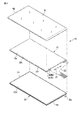
図1は、第1の実施形態に係る液晶表示装置の表示面側を示す斜視図、図2は、液晶表示装置の分解斜視図である。
液晶表示装置10は、例えばスマートフォン、タブレット端末、携帯電話機、ノートブックタイプPC、携帯型ゲーム機、電子辞書、テレビ装置、カーナビゲーションシステムなどの各種の電子機器に組み込んで使用することができる。
(First Embodiment)
FIG. 1 is a perspective view showing the display surface side of the liquid crystal display device according to the first embodiment, and FIG. 2 is an exploded perspective view of the liquid crystal display device.
The liquid
図1および図2に示すように、液晶表示装置10は、アクティブマトリクス型の液晶表示パネル(液晶パネル)12と、液晶パネル12の一方の表面である表示面12aに重ねて配置され、表示面12a全体を覆うカバーパネル14と、液晶パネル12の他方の表面である背面に対向配置されたバックライトユニット(バックライト装置)20と、を備えている。
As shown in FIGS. 1 and 2, the liquid
図4は、図1の線A−Aに沿った液晶表示装置の光源側の断面図である。図2および図4に示すように、液晶パネル12は、矩形平板状の第1基板SUB1と、第1基板SUB1に対向配置された矩形平板状の第2基板SUB2と、第1基板SUB1と第2基板SUB2との間に設けられた液晶層LQと、を備えている。第1基板SUB1および第2基板SUB2は、それぞれガラス板あるいは樹脂板等の透明な絶縁基板により形成されている。第2基板SUB2の周縁部は、シール材SEにより第1基板SUB1に貼り合わされている。第2基板SUB2の表面に偏光板PL2が貼付され、液晶パネル12の表示面12aを形成している。第1基板SUB1の表面(液晶パネル12の背面)に偏光板PL1が貼付されている。
FIG. 4 is a cross-sectional view of the liquid crystal display device along the line AA of FIG. 1 on the light source side. As shown in FIGS. 2 and 4, the
液晶パネル12では、表示面12aを平面視(液晶パネルの表面の法線方向から当該液晶パネルを視認する状態をいう。以下同様である)した状態で、シール材SEの内側となる領域に矩形状の表示領域(アクティブ領域)DAが設けられている。該表示領域DAに画像が表示される。表示領域DAの周囲に、矩形枠状の額縁領域(非表示領域)EDが設けられている。液晶パネル12は、バックライトユニット20からの光を表示領域DAに選択的に透過させることで画像を表示する透過表示機能を備えている。
In the
図示した例では、第1基板SUB1の短辺側の端部にフレキシブルプリント回路基板(FPC)22が接合され、液晶パネル12から外方に延出している。FPC22には、液晶パネル12を駆動するのに必要な信号を供給する信号供給源として、駆動ICチップ21等の半導体素子が実装されている。
In the illustrated example, a flexible printed circuit board (FPC) 22 is joined to the short side end of the first substrate SUB1 and extends outward from the
図1、図2、図4に示すように、カバーパネル14は、例えば、ガラス板製あるいはアクリル系の透明樹脂製であり、矩形板状を呈している。カバーパネル14の背面(液晶パネル12側の面、あるいは、観察者に対向する面と反対側となる面)の周縁部に枠状の遮光層RSが形成されている。なお、遮光層RSは、カバーパネル14の上面(表示面)に形成してもよい。カバーパネル14の背面(裏面)は、光透過性を有する接着剤あるいは粘着剤により、液晶パネル12の偏光板PL2に貼付されている。
As shown in FIGS. 1, 2, and 4, the
図3は、バックライトユニット20の分解斜視図である。図2、図3、図4に示すように、バックライトユニット20は、ケース23と、ケース23内に配置された複数の光学部材と、光学部材に入射する光を供給する光源ユニット30と、を備えている。本実施形態において、ケース23は、矩形状の底板17と、底板17の側縁に沿って立設された複数の側板と、側板に密着して設けられる矩形枠状のフレーム16と、を有している。これらフレーム16と底板17は、いずれも樹脂製あるいは金属製として一体に形成することが可能であり、あるいは、いずれか一方を樹脂製、他方を金属製とする構成も採用可能である。本実施形態では、底板17及び側板をステンレス(SUS)等の金属で形成し、フレーム16を樹脂で形成している。フレーム16は、インサートモールディング等により側板と一体化されている。フレーム16および側板は、互いに対向する一対の長側板16a、16bと、互いに対向する一対の短側板16c、16dと、を構成している。
なお、フレーム16は、本実施形態においては枠状に形成されているが、バックライトユニットの一対の短辺側にのみ設ける構成を採用することもできる。また、一対の短辺側のうち、一方の短辺側にのみフレームを設ける構成を採用することもできる。
FIG. 3 is an exploded perspective view of the
Although the
バックライトユニット20の光学部材は、フレーム16内で底板17上に載置された反射シートRE、導光板LG、および導光板LG上に重ねて配置された複数枚、例えば、2枚の第1光学シートOS1、第2光学シートOS2を有している。
反射シートREは、平面視で矩形状に形成され、フレーム16の内形寸法よりも僅かに小さい寸法に形成されている。反射シートREは、底板17上に載置され、底板17のほぼ全面を覆っている。
The optical member of the
The reflective sheet RE is formed in a rectangular shape in a plan view, and is formed in a dimension slightly smaller than the internal dimension of the
導光板LGは、透光性を有する樹脂、例えば、アクリル系あるいはシリコン系の樹脂、を矩形状に形成してなり、直方体状を成している。導光板LGは、出射面となる第1主面S1と、この第1主面S1の反対側の第2主面S2と、第1主面および第2主面とそれぞれ交差する複数の側面と、を有している。本実施形態では、導光板LGの短辺側の一側面を入射面EFとしている。
導光板LGは、第2主面S2側が反射シートREと対向した状態で、フレーム16内に配置され、反射シートRE上に載置されている。導光板LGの入射面EFは、フレーム16の短側板16dと隙間を空けて対向している。
The light guide plate LG is formed by forming a translucent resin, for example, an acrylic resin or a silicon resin in a rectangular shape, and has a rectangular parallelepiped shape. The light guide plate LG includes a first main surface S1 to be an emission surface, a second main surface S2 on the opposite side of the first main surface S1, and a plurality of side surfaces intersecting the first main surface and the second main surface, respectively. ,have. In the present embodiment, one side surface of the light guide plate LG on the short side is the incident surface EF.
The light guide plate LG is arranged in the
本実施形態によれば、第1光学シートOS1として拡散シートを用い、第2光学シートOS2としてプリズムシートを用いている。光学シートOS1、OS2は、導光板LGの第1主面S1上に順に重ねて載置されている。光学シートは、2枚に限らず、3枚以上あるいは2枚以下の光学シートを用いてもよい。
図4に示すように、第1光学シート(拡散シート)OS1は、光源側の端部(短辺側端部)OSEを有している。この端部OSEは、導光板LGの入射面EFを超えて、導光板LGから光源側に突出している。より具体的には、当該端部OSEが導光板LGの入射面EFと光源ユニットのLED(後述)との当接面を覆っている。端部OSEの上面(液晶パネル12側の表面)に黒色印刷BPが形成されている。黒色印刷BPは、第1光学シートOS1の短辺の全長に渡って延在している。なお、第1光学シートのうち、黒色印刷が施されている領域を端部OSEとしてよい。
更に、黒色印刷BPに重ねて帯状の遮光テープ45が貼付されている。これら黒色印刷BPおよび遮光テープ45により、拡散シートOS1の端部OSEを遮光し、端部OSEからの光漏れを抑制している。本実施形態では、遮光テープ45の幅は、黒色印刷BPの幅(すなわち端部OSEの幅)より小さい。これに対し、遮光テープ45の幅を黒色印刷BPの幅よりも大きくする構成も採用可能である。また、この遮光テープ45の端部を第1光学シートOS1よりも外方に突出させる構成も採用可能である。
According to this embodiment, a diffusion sheet is used as the first optical sheet OS1, and a prism sheet is used as the second optical sheet OS2. The optical sheets OS1 and OS2 are sequentially stacked and placed on the first main surface S1 of the light guide plate LG. The optical sheet is not limited to two, and three or more or two or less optical sheets may be used.
As shown in FIG. 4, the first optical sheet (diffusion sheet) OS1 has an end portion (short side end portion) OSE on the light source side. This end OSE extends beyond the incident surface EF of the light guide plate LG from the light guide plate LG toward the light source. More specifically, the end OSE covers the contact surface between the incident surface EF of the light guide plate LG and the LED (described later) of the light source unit. A black printing BP is formed on the upper surface (the surface on the
Further, a band-shaped light-shielding
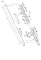
次に、バックライトユニット20の光源ユニット(光源装置)30について詳細に説明する。図5は、光源ユニットのLED実装側を示す斜視図である。
図5に示すように、光源ユニット30は、配線基板として機能する帯状のフレキシブルプリント回路基板(FPC)32と、FPC32上に実装された複数の光源と、を有している。FPC32は、ケース23の短辺とほぼ等しい長さに形成され、互いに平行に延びる一対の側縁32a、32bを有している。FPC32は、一方の側縁32bから延出した接続端部32cを一体に有している。FPC32は、導電層で形成された複数の接続パッド41および配線40を有し、接続パッド41はFPC32の一方の表面に露出している。FPC32の幅W1は、導光板LGの入射面EFと短側板16dの外面との間の距離D1(図4参照)よりも小さく形成されている。
Next, the light source unit (light source device) 30 of the
As shown in FIG. 5, the
本実施形態では、光源として、点光源である発光素子、例えば、発光ダイオード(LED)34を所定の間隔で複数個、並べたものを用いている。LED34の各々は、ほぼ直方体形状のケース(エンクロージャ)を有している。ケースは、光を出射する発光面34aと、発光面34aと直交する実装面34bと、発光面34aと直交し実装面34bに対向する第1側面34cと、を有している。実装面34bには、図示しない一対の接続端子が設けられている。
複数のLED34は、実装面34b側がFPC32の一方の表面上にそれぞれ実装されている。具体的には、LED34の一対の接続端子は、FPC32の接続パッド41に電気的、機械的に接合されている。LED34は、発光面34aを含む端部が、FPC32の側縁32aから外側に突出した状態でFPC32に実装されている。発光面34aは、側縁32aから離間し、かつ、側縁32aとほぼ平行に位置している。
In the present embodiment, as the light source, a light emitting element which is a point light source, for example, a plurality of light emitting diodes (LEDs) 34 arranged at predetermined intervals are used. Each of the
The plurality of
複数のLED34は、FPC32の長手方向(側縁32a、32bと平行な方向、あるいは、フレーム16の短側板16dと平行な方向)に沿って互いに所定の間隔をおいて並んでいる。複数のLED34の発光面34aは、側縁32aに沿ってほぼ面一に並んでいる。LED34の配列ピッチ、隣合う2つのLED34間の間隔は、適宜設定可能である。上述の如く、FPC32の幅W1は可及的小さく形成され、その結果としてLED34の発光面34aがFPC32から突出するものとなっている。なお、当該FPC32の幅W1は、LED34の発光面34aからの奥行の1〜1.5倍程度の大きさが好ましい。
上記のように構成された光源ユニット30は、ケース23内に配置され、更に、固定テープTP2により、導光板LGに固定、支持される。
The plurality of
The
図4に示すように、光源ユニット30は、ケース23内に配置されている。すなわち、複数のLED34は、ケース23内で、導光板LGの入射面EFと短側板16dとの間に配置され、LED34の発光面34aは、入射面EFと平行に隣接対向し、あるいは、入射面EFに平行に当接している。FPC32は短側板16dに沿って配置され、側縁32b側の側縁部が短側板16d上に載置されている。FPC32は、第1光学シートOS1とほぼ同一平面上に位置し、LED34を挟んで底板17に対向している。FPC32の側縁32aは、入射面EFから短側板16d側に離間して位置し、第1光学シートOS1の端部OSEに隙間を置いて対向している。なお、FPC32の側縁部は、接着剤(粘着テープ)42によりフレーム16上に貼付してもよい。
As shown in FIG. 4, the
LED34の第1側面34cは、導光板LGの第2主面S2とほぼ面一に並んでいる。第1側面34cおよび導光板LGの第2主面S2に亘って固定テープTP2が貼付されている。複数のLED34は、固定テープTP2により導光板LGに固定され、所定位置に支持されている。固定テープTP2は、例えば、ポリエチレンテレフタレート(PET)等で形成された帯状の基材42aと、基材42aに重ねて形成された帯状の粘着シート42bと、を有している。粘着シート42bは、一例では、ポリウレタン等で形成された熱反応型の粘着シートを用いている。粘着シート42bは、約70〜120℃程度に加熱すると、接着対象物との反応により接着力を発生する。熱反応型の粘着シート42bは、一般的な両面テープの約3〜5倍程度の接着力を発生することができる。粘着シート42bは、透明でもよいし、あるいは、黒インク等を含有した黒色とし遮光機能を有していてもよい。
なお、固定テープTP2はLED34から導光板LGに跨って設けられ、これらを互いに当接した状態で固定するためのものであるが、当該固定テープTP2は底板17には接着されていない。
The
The fixing tape TP2 is provided so as to straddle the light guide plate LG from the
固定テープTP2は、LED34の幅よりも大きな幅W2、および導光板LGの短辺とほぼ等しい長さL(図5参照)を有している。固定テープTP2は、導光板LGの短辺に沿って配置され、粘着シート42bの幅方向ほぼ半分の領域が複数のLED34の第1側面34cに貼付されている。粘着シート42bの残りの領域は、導光板LGの第2主面S2に貼付されている。
上述したように、粘着シート42bは、強い接着力を発生するため、比較的小さな接着面積に貼付した場合でも、強固に接着することができる。従って、固定テープTP2により、複数のLED34を導光板LGに強固に固定し、所定位置に安定して保持することが可能である。なお、前述したFPC32を短側板16dに貼付する接着剤として、上記熱反応型の粘着シートを用いてもよい。
The fixing tape TP2 has a width W2 larger than the width of the
As described above, since the
図2および図3に示すように、バックライトユニット20は、枠状の両面テープTP1を備えている。両面テープTP1は、フレーム16上に貼付されている。
図4に示すように、ケース23の光源側端部において、両面テープTP1は、スペーサSP1を介して、FPC32上に貼付され、更に、遮光テープ45上に貼付されている。
As shown in FIGS. 2 and 3, the
As shown in FIG. 4, at the light source side end portion of the
上記のように構成されたバックライトユニット20は、両面テープTP1により、液晶パネル12に取り付けられている。両面テープTP1の内周部は偏光板PL1に貼り付けられ、外周部は、スペーサSP2を挟んで、第1基板SUB1に貼り付けられている。バックライトユニット20の外周縁は、第1基板SUB1の外周縁に一致している。
光源ユニット30のFPC32は、接続端部32cを介してFPC22に接続されている(図1、図2参照)。FPC22およびFPC32を介してLED34に駆動電流が通電することにより、LED34が点灯する。LED34から出射された光は、入射面EFから導光板LG内に入射し、導光板LG内を伝播し、或いは反射シートREで反射され、第1主面(出射面)S1から液晶パネル12側に出射される。
The
The
以上のように構成された本実施形態に係るバックライトユニット20および液晶表示装置10によれば、光源ユニット30のLED34は、固定テープTP2により導光板LGに強固に固定され、所定位置に保持される。そのため、光源ユニット30のFPC(配線基板)32に、光源ユニット30を支持および固定する機能を持たせる必要がなく、FPC32の幅W1を大幅に削減することが可能となる。FPC32の幅W1を小さくすることにより、ケース23の短側板16dと導光板LGの入射面EFとの間隔を短くすることができる。これにより、バックライトユニット20の光源側の額縁幅および液晶表示装置10の光源側の額縁幅を小さくし、狭額縁化を図ることができる。
FPC32は、導光板LGに重なることなく、入射面EFから離間している。そのため、バックライトユニット20の薄型化が可能となる。
According to the
The
また、入射面EF側から見た場合に、FPC32の側縁32aがLED34の発光面34aよりも後退した位置となるため、LED34の発光面34aからの光が上方に漏れることが考えられる。これに対し、本実施形態では、第1光学シート(拡散シート)OS1は、光源側端部OSEを有し、当該光源側端部OSEは、入射面EFを超えて導光板LGから延出し、入射面EFおよびLED34の発光面34aを覆っている。光源側端部OSE上に黒色印刷BPおよび遮光テープ45を設けることにより、光源側端部OSEに遮光機能を持たせている。従って、FPC32と入射面EFとの間の隙間を第1光学シートOS1の光源側端部OSEによって遮光し、LED34からの光漏れを防止することができる。
このように、従来の構成では、光源ユニットの配線基板(FPC)に、LEDを固定および電気接続する機能のみならず、LEDからの光を遮光する機能やLEDを導光板に当接した状態で固定する機能を付与していたが、本実施形態においては、FPC32にはLED34への通電機能だけに特化させ、遮光機能は光学シートOS1に、固定機能は固定テープTP2に付与するものとなっている。具体的には、光学シートOS1を導光板LGよりも突出させると共に遮光領域を形成することで、遮光機能を付与している。また、LED34から見て固定テープTP2をFPC32とは反対側(反射シート側)に設け、当該遮光テープTP2に粘着性の高い粘着シートを採用することで、単一での固定機能を付与しているのである。この結果、FPC32の大幅な小型化が可能となり、結果として液晶表示パネルの光源側の狭額縁化が図れるものとなっている。
以上のことから、本実施形態によれば、狭額縁化および薄型化が可能なバックライト装置および液晶表示装置が得られる。
Further, when viewed from the incident surface EF side, the
As described above, in the conventional configuration, not only the function of fixing and electrically connecting the LED to the wiring board (FPC) of the light source unit, but also the function of blocking the light from the LED and the state where the LED is in contact with the light guide plate. Although the function of fixing was given, in the present embodiment, the
From the above, according to the present embodiment, a backlight device and a liquid crystal display device capable of narrowing the frame and making the frame thinner can be obtained.
本発明の実施形態を説明したが、この実施形態は、例として提示したものであり、発明の範囲を限定することは意図していない。新規な実施形態および変形例は、その他の様々な形態で実施されることが可能であり、発明の要旨を逸脱しない範囲で、種々の省略、置き換え、変更を行うことができる。実施形態やその変形例は、発明の範囲や要旨に含まれるとともに、特許請求の範囲に記載された発明とその均等の範囲に含まれる。 Although embodiments of the present invention have been described, these embodiments are presented as examples and are not intended to limit the scope of the invention. The novel embodiments and modifications can be implemented in various other embodiments, and various omissions, replacements, and changes can be made without departing from the gist of the invention. The embodiments and variations thereof are included in the scope and gist of the invention, and are also included in the scope of the invention described in the claims and the equivalent scope thereof.
本発明の実施形態として上述した各構成を基にして、当業者が適宜設計変更して実施し得る全ての構成も、本発明の要旨を包含する限り、本発明の範囲に属する。例えば、液晶パネル、バックライトユニットの構成部材、およびケースの外形状および内形状は、矩形状に限定されることなく、外形あるいは内形のいずれか一方あるいは両方を平面視で多角形状や円形、楕円形、およびこれらを組み合わせた形状等の他の形状としてもよい。液晶表示装置およびバックライト装置は、平坦な形状に限らず、一部あるいは全部が湾曲あるいは傾斜した形状としてもよい。構成部材の材料は、上述した例に限らず、種々選択可能である。
上述した実施形態によりもたらされる他の作用効果について本明細書の記載から明らかなもの、又は当業者において適宜想到し得るものついては、当然に本発明によりもたらされるものと解される。
All configurations that can be appropriately designed and implemented by those skilled in the art based on the configurations described above as embodiments of the present invention also belong to the scope of the present invention as long as the gist of the present invention is included. For example, the outer and inner shapes of the liquid crystal panel, the constituent members of the backlight unit, and the case are not limited to a rectangular shape, and either the outer shape or the inner shape, or both, may be polygonal or circular in a plan view. Other shapes such as an elliptical shape and a shape in which these are combined may be used. The liquid crystal display device and the backlight device are not limited to a flat shape, and may have a partially or completely curved or inclined shape. The material of the constituent member is not limited to the above-mentioned example, and various materials can be selected.
Other effects brought about by the above-described embodiments are clearly understood from the description of the present specification, or those which can be appropriately conceived by those skilled in the art are naturally understood to be brought about by the present invention.
10…液晶表示装置、12…液晶パネル、14…カバーパネル、
16…フレーム、20…バックライトユニット(バックライト装置)、23…ケース、
30…光源ユニット(光源装置)、32…配線基板(FPC)、34…LED、
34a…発光面、34b…実装面、34c…第1側面、TP2…固定テープ、
42a…基材、42b…粘着シート、SUB1…第1基板、
SUB2…第2基板、LQ…液晶層、DA…表示領域、
ED…額縁領域(非表示領域)、LG…導光板、EF…入射面
OS1…第1光学シート、OS2…第2光学シート
10 ... Liquid crystal display device, 12 ... Liquid crystal panel, 14 ... Cover panel,
16 ... frame, 20 ... backlight unit (backlight device), 23 ... case,
30 ... Light source unit (light source device), 32 ... Wiring board (FPC), 34 ... LED,
34a ... light emitting surface, 34b ... mounting surface, 34c ... first side surface, TP2 ... fixing tape,
42a ... base material, 42b ... adhesive sheet, SUB1 ... first substrate,
SUB2 ... second substrate, LQ ... liquid crystal layer, DA ... display area,
ED ... Frame area (non-display area), LG ... Light guide plate, EF ... Incident surface
OS1 ... 1st optical sheet, OS2 ... 2nd optical sheet
Claims (7)
出射面を構成する第1主面と、前記第1主面と対向する第2主面と、前記第1主面および第2主面と交差する入射面と、を有し、前記第2主面が前記底板上に配置される導光板と、
配線を有する配線基板と前記配線基板に実装された複数の発光素子と、を有し、前記導光板の入射面に光を入射する光源ユニットと、を備え、
前記配線基板は、前記入射面に沿って延在しているとともに前記入射面から離間して位置する側縁を有し、前記発光素子を挟んで前記底板に対向し、かつ、前記導光板から離間して配置され、
前記発光素子は、前記配線基板に一部が実装され前記側縁から前記導光板の側に延出した実装面と、前記実装面と交差する方向に延在し前記側縁から前記導光板側に突出して位置した発光面と、前記発光面と交差し前記実装面と対向した第1側面と、を有し、
前記発光素子は、前記発光面が前記導光板の入射面と対向し、前記第1側面が前記第2主面と平行に並んで配置され、前記第1側面および前記第2主面に亘って貼付された固定テープにより前記導光板に固定されているバックライト装置。 A case with a bottom plate and
It has a first main surface constituting an emission surface, a second main surface facing the first main surface, and an incident surface intersecting the first main surface and the second main surface, and the second main surface. A light guide plate whose surface is arranged on the bottom plate, and
A wiring board having wiring, a plurality of light emitting elements mounted on the wiring board, and a light source unit for incident light on an incident surface of the light guide plate.
The wiring board has a side edge extending along the incident surface and located away from the incident surface, facing the bottom plate with the light emitting element interposed therebetween, and from the light guide plate. Arranged apart,
The light emitting element has a mounting surface that is partially mounted on the wiring board and extends from the side edge to the light guide plate side, and extends in a direction intersecting the mounting surface and extends from the side edge to the light guide plate side. It has a light emitting surface protruding from the light emitting surface and a first side surface that intersects with the light emitting surface and faces the mounting surface.
In the light emitting element, the light emitting surface faces the incident surface of the light guide plate, the first side surface is arranged side by side in parallel with the second main surface, and the light emitting element extends over the first side surface and the second main surface. A backlight device fixed to the light guide plate by a fixed tape attached.
前記光学シートは、前記入射面から前記発光素子側に突出し前記発光素子の実装面と対向した光源側端部を有している請求項1に記載のバックライト装置。 Further, an optical sheet arranged on the first main surface of the light guide plate is further provided.
The backlight device according to claim 1 , wherein the optical sheet projects from the incident surface toward the light emitting element and has a light source side end portion facing the mounting surface of the light emitting element.
前記配線基板の一部は、前記側板上に配置され、接着剤で前記側板に貼付されている請求項1に記載のバックライト装置。 The case has side plates that are erected along the side edges of the bottom plate and face the light emitting element with a gap.
The backlight device according to claim 1, wherein a part of the wiring board is arranged on the side plate and is attached to the side plate with an adhesive.
前記液晶パネルに対向して設けられた請求項1から6のいずれか1項に記載のバックライト装置と、
を備える液晶表示装置。 LCD panel and
The backlight device according to any one of claims 1 to 6 , which is provided so as to face the liquid crystal panel.
A liquid crystal display device.
Priority Applications (5)
| Application Number | Priority Date | Filing Date | Title |
|---|---|---|---|
| JP2017226210A JP6971802B2 (en) | 2017-11-24 | 2017-11-24 | Backlight device and liquid crystal display device |
| US16/196,428 US10948768B2 (en) | 2017-11-24 | 2018-11-20 | Backlight device and liquid crystal display device |
| US17/200,224 US11209695B2 (en) | 2017-11-24 | 2021-03-12 | Backlight device and a liquid crystal display device |
| US17/545,560 US11686972B2 (en) | 2017-11-24 | 2021-12-08 | Backlight device |
| US18/197,346 US11874553B2 (en) | 2017-11-24 | 2023-05-15 | Backlight device |
Applications Claiming Priority (1)
| Application Number | Priority Date | Filing Date | Title |
|---|---|---|---|
| JP2017226210A JP6971802B2 (en) | 2017-11-24 | 2017-11-24 | Backlight device and liquid crystal display device |
Publications (2)
| Publication Number | Publication Date |
|---|---|
| JP2019096525A JP2019096525A (en) | 2019-06-20 |
| JP6971802B2 true JP6971802B2 (en) | 2021-11-24 |
Family
ID=66632349
Family Applications (1)
| Application Number | Title | Priority Date | Filing Date |
|---|---|---|---|
| JP2017226210A Active JP6971802B2 (en) | 2017-11-24 | 2017-11-24 | Backlight device and liquid crystal display device |
Country Status (2)
| Country | Link |
|---|---|
| US (4) | US10948768B2 (en) |
| JP (1) | JP6971802B2 (en) |
Families Citing this family (5)
| Publication number | Priority date | Publication date | Assignee | Title |
|---|---|---|---|---|
| JP6971802B2 (en) * | 2017-11-24 | 2021-11-24 | 株式会社ジャパンディスプレイ | Backlight device and liquid crystal display device |
| CN211123566U (en) * | 2020-01-20 | 2020-07-28 | 京东方科技集团股份有限公司 | Backlight module and display device |
| CN112051688B (en) * | 2020-09-11 | 2022-09-16 | 深圳市利航电子有限公司 | Backlight source for AR glasses |
| JP2023003910A (en) * | 2021-06-25 | 2023-01-17 | 株式会社ジャパンディスプレイ | Display device |
| WO2024040725A1 (en) * | 2022-08-22 | 2024-02-29 | 瑞仪(广州)光电子器件有限公司 | Backlight module and display device |
Family Cites Families (11)
| Publication number | Priority date | Publication date | Assignee | Title |
|---|---|---|---|---|
| JPH10247412A (en) | 1997-03-03 | 1998-09-14 | Omron Corp | Surface light source device |
| JP2003076287A (en) | 2001-09-04 | 2003-03-14 | Sony Corp | Backlight device |
| JP2007026859A (en) | 2005-07-15 | 2007-02-01 | Minebea Co Ltd | Planar lighting fixture |
| KR101313653B1 (en) * | 2009-06-24 | 2013-10-02 | 엘지디스플레이 주식회사 | Liquid crystal display device |
| JP6303646B2 (en) | 2014-03-13 | 2018-04-04 | オムロン株式会社 | Surface light source device |
| CN104456302B (en) | 2014-11-17 | 2017-03-08 | 深圳市华星光电技术有限公司 | Backlight module and display |
| JP6284277B2 (en) | 2015-04-15 | 2018-02-28 | ミネベアミツミ株式会社 | Surface lighting device |
| KR102377116B1 (en) * | 2015-06-29 | 2022-03-22 | 엘지디스플레이 주식회사 | Circuit Device Emitting Heat and Backlight Unit Comprising Thereof |
| JP2017157467A (en) | 2016-03-03 | 2017-09-07 | オムロン株式会社 | Surface light source device, display device, and electronic equipment |
| JP6709768B2 (en) | 2017-09-28 | 2020-06-17 | ミネベアミツミ株式会社 | Area lighting device |
| JP6971802B2 (en) * | 2017-11-24 | 2021-11-24 | 株式会社ジャパンディスプレイ | Backlight device and liquid crystal display device |
-
2017
- 2017-11-24 JP JP2017226210A patent/JP6971802B2/en active Active
-
2018
- 2018-11-20 US US16/196,428 patent/US10948768B2/en active Active
-
2021
- 2021-03-12 US US17/200,224 patent/US11209695B2/en active Active
- 2021-12-08 US US17/545,560 patent/US11686972B2/en active Active
-
2023
- 2023-05-15 US US18/197,346 patent/US11874553B2/en active Active
Also Published As
| Publication number | Publication date |
|---|---|
| US20230280614A1 (en) | 2023-09-07 |
| US11686972B2 (en) | 2023-06-27 |
| JP2019096525A (en) | 2019-06-20 |
| US20210200025A1 (en) | 2021-07-01 |
| US20190163014A1 (en) | 2019-05-30 |
| US20220100034A1 (en) | 2022-03-31 |
| US11209695B2 (en) | 2021-12-28 |
| US10948768B2 (en) | 2021-03-16 |
| US11874553B2 (en) | 2024-01-16 |
Similar Documents
| Publication | Publication Date | Title |
|---|---|---|
| US10281636B2 (en) | Back light | |
| JP6971802B2 (en) | Backlight device and liquid crystal display device | |
| JP7043267B2 (en) | Display device | |
| TWI655481B (en) | Backlight device and liquid crystal display device including the same | |
| JP5091602B2 (en) | Surface light source device and liquid crystal display device using the same | |
| US10545281B2 (en) | Backlight device and liquid crystal display device comprising the same | |
| US10551556B2 (en) | Light source device and light source unit comprising the same | |
| US10739514B2 (en) | Light source device, backlight device comprising the same and liquid crystal display device | |
| JP2019139072A (en) | Display device and flexible wiring board | |
| KR102538982B1 (en) | Liquid crystal display module and liquid crystal display apparatus using the same | |
| JP7086717B2 (en) | Light source device, backlight device equipped with this, and liquid crystal display device | |
| JP2018014315A (en) | Backlight device and liquid crystal display device including the same | |
| JP2018026324A (en) | Backlight device and liquid crystal display including the same | |
| JP2017188304A (en) | Backlight device and display device including the same | |
| WO2020153090A1 (en) | Liquid crystal display device | |
| US10725232B2 (en) | Backlight device and liquid crystal display device comprising the same | |
| JP2014085545A (en) | Liquid crystal display device | |
| JP7102296B2 (en) | Display device | |
| US20180011241A1 (en) | Backlight device and liquid crystal display device with the same | |
| JP7110427B2 (en) | BACKLIGHT DEVICE AND LIQUID CRYSTAL DISPLAY DEVICE WITH THE SAME |
Legal Events
| Date | Code | Title | Description |
|---|---|---|---|
| A621 | Written request for application examination |
Free format text: JAPANESE INTERMEDIATE CODE: A621 Effective date: 20200708 |
|
| A977 | Report on retrieval |
Free format text: JAPANESE INTERMEDIATE CODE: A971007 Effective date: 20210520 |
|
| A131 | Notification of reasons for refusal |
Free format text: JAPANESE INTERMEDIATE CODE: A131 Effective date: 20210525 |
|
| A521 | Request for written amendment filed |
Free format text: JAPANESE INTERMEDIATE CODE: A523 Effective date: 20210713 |
|
| TRDD | Decision of grant or rejection written | ||
| A01 | Written decision to grant a patent or to grant a registration (utility model) |
Free format text: JAPANESE INTERMEDIATE CODE: A01 Effective date: 20211005 |
|
| A61 | First payment of annual fees (during grant procedure) |
Free format text: JAPANESE INTERMEDIATE CODE: A61 Effective date: 20211102 |
|
| R150 | Certificate of patent or registration of utility model |
Ref document number: 6971802 Country of ref document: JP Free format text: JAPANESE INTERMEDIATE CODE: R150 |