JP7081628B2 - 発光装置、および電子機器 - Google Patents
発光装置、および電子機器 Download PDFInfo
- Publication number
- JP7081628B2 JP7081628B2 JP2020133672A JP2020133672A JP7081628B2 JP 7081628 B2 JP7081628 B2 JP 7081628B2 JP 2020133672 A JP2020133672 A JP 2020133672A JP 2020133672 A JP2020133672 A JP 2020133672A JP 7081628 B2 JP7081628 B2 JP 7081628B2
- Authority
- JP
- Japan
- Prior art keywords
- light emitting
- layer
- electrode
- view
- plan
- Prior art date
- Legal status (The legal status is an assumption and is not a legal conclusion. Google has not performed a legal analysis and makes no representation as to the accuracy of the status listed.)
- Active
Links
- 239000000758 substrate Substances 0.000 claims description 79
- 238000007789 sealing Methods 0.000 claims description 40
- 239000010410 layer Substances 0.000 description 198
- 239000012044 organic layer Substances 0.000 description 21
- 239000004065 semiconductor Substances 0.000 description 21
- 239000000463 material Substances 0.000 description 16
- 238000005401 electroluminescence Methods 0.000 description 11
- 239000000470 constituent Substances 0.000 description 9
- 230000007547 defect Effects 0.000 description 9
- 230000003287 optical effect Effects 0.000 description 8
- 229910052581 Si3N4 Inorganic materials 0.000 description 7
- HQVNEWCFYHHQES-UHFFFAOYSA-N silicon nitride Chemical compound N12[Si]34N5[Si]62N3[Si]51N64 HQVNEWCFYHHQES-UHFFFAOYSA-N 0.000 description 7
- 238000000034 method Methods 0.000 description 6
- 230000004048 modification Effects 0.000 description 6
- 238000012986 modification Methods 0.000 description 6
- 238000010586 diagram Methods 0.000 description 5
- VYPSYNLAJGMNEJ-UHFFFAOYSA-N Silicium dioxide Chemical compound O=[Si]=O VYPSYNLAJGMNEJ-UHFFFAOYSA-N 0.000 description 4
- XUIMIQQOPSSXEZ-UHFFFAOYSA-N Silicon Chemical compound [Si] XUIMIQQOPSSXEZ-UHFFFAOYSA-N 0.000 description 4
- 239000000853 adhesive Substances 0.000 description 4
- 230000001070 adhesive effect Effects 0.000 description 4
- 229910052710 silicon Inorganic materials 0.000 description 4
- 239000010703 silicon Substances 0.000 description 4
- 230000007423 decrease Effects 0.000 description 3
- 238000002347 injection Methods 0.000 description 3
- 239000007924 injection Substances 0.000 description 3
- 229910010272 inorganic material Inorganic materials 0.000 description 3
- 239000011147 inorganic material Substances 0.000 description 3
- 239000011810 insulating material Substances 0.000 description 3
- 239000002346 layers by function Substances 0.000 description 3
- 239000011347 resin Substances 0.000 description 3
- 229920005989 resin Polymers 0.000 description 3
- 229910052814 silicon oxide Inorganic materials 0.000 description 3
- 239000004925 Acrylic resin Substances 0.000 description 2
- 229920000178 Acrylic resin Polymers 0.000 description 2
- 239000000956 alloy Substances 0.000 description 2
- 229910045601 alloy Inorganic materials 0.000 description 2
- 230000005540 biological transmission Effects 0.000 description 2
- 239000004020 conductor Substances 0.000 description 2
- 230000007797 corrosion Effects 0.000 description 2
- 238000005260 corrosion Methods 0.000 description 2
- 230000002950 deficient Effects 0.000 description 2
- 238000001514 detection method Methods 0.000 description 2
- 239000003822 epoxy resin Substances 0.000 description 2
- 239000011521 glass Substances 0.000 description 2
- 238000004519 manufacturing process Methods 0.000 description 2
- 229910052751 metal Inorganic materials 0.000 description 2
- 239000002184 metal Substances 0.000 description 2
- 230000003647 oxidation Effects 0.000 description 2
- 238000007254 oxidation reaction Methods 0.000 description 2
- 238000005192 partition Methods 0.000 description 2
- 229920000647 polyepoxide Polymers 0.000 description 2
- 229910052709 silver Inorganic materials 0.000 description 2
- 239000004332 silver Substances 0.000 description 2
- 239000012808 vapor phase Substances 0.000 description 2
- FYYHWMGAXLPEAU-UHFFFAOYSA-N Magnesium Chemical compound [Mg] FYYHWMGAXLPEAU-UHFFFAOYSA-N 0.000 description 1
- 229910052782 aluminium Inorganic materials 0.000 description 1
- XAGFODPZIPBFFR-UHFFFAOYSA-N aluminium Chemical compound [Al] XAGFODPZIPBFFR-UHFFFAOYSA-N 0.000 description 1
- QVGXLLKOCUKJST-UHFFFAOYSA-N atomic oxygen Chemical compound [O] QVGXLLKOCUKJST-UHFFFAOYSA-N 0.000 description 1
- 230000004888 barrier function Effects 0.000 description 1
- 239000000919 ceramic Substances 0.000 description 1
- 239000007789 gas Substances 0.000 description 1
- 230000012447 hatching Effects 0.000 description 1
- 230000005525 hole transport Effects 0.000 description 1
- 238000005286 illumination Methods 0.000 description 1
- 229910052738 indium Inorganic materials 0.000 description 1
- APFVFJFRJDLVQX-UHFFFAOYSA-N indium atom Chemical compound [In] APFVFJFRJDLVQX-UHFFFAOYSA-N 0.000 description 1
- AMGQUBHHOARCQH-UHFFFAOYSA-N indium;oxotin Chemical compound [In].[Sn]=O AMGQUBHHOARCQH-UHFFFAOYSA-N 0.000 description 1
- 238000007733 ion plating Methods 0.000 description 1
- 238000010030 laminating Methods 0.000 description 1
- 238000000608 laser ablation Methods 0.000 description 1
- 239000007791 liquid phase Substances 0.000 description 1
- 229910052749 magnesium Inorganic materials 0.000 description 1
- 239000011777 magnesium Substances 0.000 description 1
- 239000011159 matrix material Substances 0.000 description 1
- 150000002736 metal compounds Chemical class 0.000 description 1
- 150000002739 metals Chemical class 0.000 description 1
- 239000011368 organic material Substances 0.000 description 1
- 239000001301 oxygen Substances 0.000 description 1
- 229910052760 oxygen Inorganic materials 0.000 description 1
- 238000007639 printing Methods 0.000 description 1
- 239000010453 quartz Substances 0.000 description 1
- 238000007650 screen-printing Methods 0.000 description 1
- 229920002050 silicone resin Polymers 0.000 description 1
- 238000004544 sputter deposition Methods 0.000 description 1
- 229920002803 thermoplastic polyurethane Polymers 0.000 description 1
- 238000007740 vapor deposition Methods 0.000 description 1
Images


Description
1-1.第1実施形態
本発明の発光装置の一例として、画像を表示する有機EL表示装置を例に説明する。
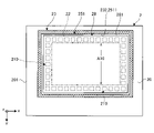
図1は、第1実施形態に係る発光装置を示す平面図である。なお、以下では、説明の便宜上、図1に示す互いに直交するx軸、y軸およびz軸を適宜用いて説明する。なお、z軸のうち矢印の方向が+z方向でありこれを「上側」とし、z軸のうち矢印とは反対方向が-z方向でありこれを「下側」とする。また、本明細書では、-z方向から見ることを「平面視」という。また、x-y平面に平行な方向から見ることを「断面視」という。
図2は、第1実施形態における表示パネルの電気的な構成を示すブロック図である。なお、以下では、説明の便宜上、図2に示す互いに直交するX軸およびY軸を適宜用いて説明する。
次に、表示パネルの構成を簡単に説明する。図4は、第1実施形態に係る発光装置の部分断面図である。なお、z軸のうち矢印の方向が+z方向でありこれを「上側」とし、z軸のうち矢印とは反対方向が-z方向でありこれを「下側」とする。
図5は、第1実施形態における素子基板の一部を示す概略断面図である。図6は、第1実施形態における有機層と平坦化層との配置を説明するための概略平面図である。また、図5では、有機層25のうち発光層251以外の層の図示は省略する。図6では、コンタクト部23に網掛けを付す。
次に、本発明の第2実施形態について説明する。図8は、第2実施形態における素子基板の一部を示す概略断面図である。
次に、本発明の第3実施形態について説明する。図9は、第3実施形態における素子基板の一部を示す概略断面図である。
以上に例示した各実施形態は多様に変形され得る。前述の各形態に適用され得る具体的な変形の態様を以下に例示する。以下の例示から任意に選択された2以上の態様は、相互に矛盾しない範囲で適宜に併合され得る。
前述の実施形態または変形例の発光装置100は、それぞれ、各種の電子機器に適用することができ、特に2K2K以上の高精細な画像の表示を要求され、かつ小型であることを要求される電子機器に好適である。
Claims (8)
- 基板と、
第1の電極と、
第2の電極と、
前記第1の電極と前記第2の電極との間に設けられた発光層と、
前記第2の電極の前記発光層とは反対側に設けられた平坦化層を含む封止層と、
前記第1の電極と同層に設けられ、平面視において前記第1の電極と前記基板の外縁との間に設けられるダミー電極と、
を備え、
平面視において、前記平坦化層の外縁は、前記発光層と重なり、
平面視において、前記平坦化層の外縁は、前記ダミー電極の外縁と前記発光層の外縁との間に位置する、
発光装置。 - 前記基板と前記平坦化層との間に設けられ、配線と前記第2の電極との間を電気的に接続させるコンタクト部を有する、
請求項1に記載の発光装置。 - 平面視において、前記平坦化層の外縁は、前記ダミー電極と前記コンタクト部との間に位置する、
請求項2に記載の発光装置。 - 平面視において、前記平坦化層は、前記ダミー電極の全体と重なる、
請求項1ないし3のいずれか1項に記載の発光装置。 - 基板と、
第1の電極と、
第2の電極と、
前記第1の電極と前記第2の電極との間に設けられた発光層と、
前記第2の電極の前記発光層とは反対側に設けられた平坦化層を含む封止層と、
前記第1の電極と同層に設けられ、平面視において前記第1の電極と前記基板の外縁との間に設けられるダミー電極と、
を備え、
平面視において、前記平坦化層の外縁は、前記発光層と重なり、
平面視において、前記ダミー電極の外縁は、前記平坦化層の外縁と前記発光層の外縁との間に位置する、
発光装置。 - 前記基板と前記平坦化層との間に設けられ、配線と前記第2の電極との間を電気的に接続させるコンタクト部を有する、
請求項5に記載の発光装置。 - 平面視において、前記平坦化層は、前記ダミー電極の一部と重なる、
請求項5または6に記載の発光装置。 - 請求項1ないし7のいずれか1項に記載の発光装置を備える電子機器。
Priority Applications (1)
| Application Number | Priority Date | Filing Date | Title |
|---|---|---|---|
| JP2020133672A JP7081628B2 (ja) | 2020-08-06 | 2020-08-06 | 発光装置、および電子機器 |
Applications Claiming Priority (1)
| Application Number | Priority Date | Filing Date | Title |
|---|---|---|---|
| JP2020133672A JP7081628B2 (ja) | 2020-08-06 | 2020-08-06 | 発光装置、および電子機器 |
Related Parent Applications (1)
| Application Number | Title | Priority Date | Filing Date |
|---|---|---|---|
| JP2018156999A Division JP6750651B2 (ja) | 2018-08-24 | 2018-08-24 | 発光装置、および電子機器 |
Publications (3)
| Publication Number | Publication Date |
|---|---|
| JP2020177933A JP2020177933A (ja) | 2020-10-29 |
| JP2020177933A5 JP2020177933A5 (ja) | 2021-09-09 |
| JP7081628B2 true JP7081628B2 (ja) | 2022-06-07 |
Family
ID=72916238
Family Applications (1)
| Application Number | Title | Priority Date | Filing Date |
|---|---|---|---|
| JP2020133672A Active JP7081628B2 (ja) | 2020-08-06 | 2020-08-06 | 発光装置、および電子機器 |
Country Status (1)
| Country | Link |
|---|---|
| JP (1) | JP7081628B2 (ja) |
Families Citing this family (1)
| Publication number | Priority date | Publication date | Assignee | Title |
|---|---|---|---|---|
| CN115769703A (zh) * | 2021-06-25 | 2023-03-07 | 京东方科技集团股份有限公司 | 显示基板及其制作方法、显示装置 |
Citations (4)
| Publication number | Priority date | Publication date | Assignee | Title |
|---|---|---|---|---|
| JP2004127607A (ja) | 2002-09-30 | 2004-04-22 | Seiko Epson Corp | 電気光学装置およびその製造方法、電子機器 |
| JP2007157606A (ja) | 2005-12-08 | 2007-06-21 | Seiko Epson Corp | 発光装置、発光装置の製造方法、及び電子機器 |
| JP2007265792A (ja) | 2006-03-28 | 2007-10-11 | Dainippon Printing Co Ltd | 有機エレクトロルミネッセンス素子 |
| US20180151831A1 (en) | 2016-11-30 | 2018-05-31 | Lg Display Co., Ltd. | Organic light-emitting display device |
Family Cites Families (1)
| Publication number | Priority date | Publication date | Assignee | Title |
|---|---|---|---|---|
| JP4428005B2 (ja) * | 2003-09-04 | 2010-03-10 | セイコーエプソン株式会社 | 電気光学装置、電気光学装置の製造方法、及び電子機器 |
-
2020
- 2020-08-06 JP JP2020133672A patent/JP7081628B2/ja active Active
Patent Citations (4)
| Publication number | Priority date | Publication date | Assignee | Title |
|---|---|---|---|---|
| JP2004127607A (ja) | 2002-09-30 | 2004-04-22 | Seiko Epson Corp | 電気光学装置およびその製造方法、電子機器 |
| JP2007157606A (ja) | 2005-12-08 | 2007-06-21 | Seiko Epson Corp | 発光装置、発光装置の製造方法、及び電子機器 |
| JP2007265792A (ja) | 2006-03-28 | 2007-10-11 | Dainippon Printing Co Ltd | 有機エレクトロルミネッセンス素子 |
| US20180151831A1 (en) | 2016-11-30 | 2018-05-31 | Lg Display Co., Ltd. | Organic light-emitting display device |
Also Published As
| Publication number | Publication date |
|---|---|
| JP2020177933A (ja) | 2020-10-29 |
Similar Documents
| Publication | Publication Date | Title |
|---|---|---|
| US10026800B2 (en) | Light emitting device and electronic apparatus | |
| US10490776B2 (en) | Electro-optical apparatus, manufacturing method thereof, and electronic device | |
| US11925089B2 (en) | Electro-optical device and electronic device | |
| JP2006251774A (ja) | 電気光学装置 | |
| JP2019012621A (ja) | 電気光学装置、および電子機器 | |
| JP6930565B2 (ja) | 電気光学装置 | |
| US10861915B2 (en) | Light-emitting device and electronic apparatus | |
| US10810924B2 (en) | Electro-optical device and electronic apparatus | |
| US10236473B2 (en) | Electro-optical device, electro-optical device manufacturing method, and electronic apparatus | |
| JP7081628B2 (ja) | 発光装置、および電子機器 | |
| JP6844283B2 (ja) | 電気光学装置、及び、電子機器 | |
| US20180138245A1 (en) | Electro-optical device, method for manufacturing electro-optical device, and electronic apparatus | |
| JP2007156388A (ja) | 発光装置および電子機器 | |
| JP7050772B2 (ja) | 表示装置及び電子機器 | |
| JP2012252822A (ja) | 発光装置および電子機器 | |
| US11545531B2 (en) | Display device comprising a conductor having a width of the first portion in the second direction being greater than a width of the second portion in the first direction | |
| US20230309349A1 (en) | Electro-optical device and electronic apparatus | |
| US20230110908A1 (en) | Electro-optical device and electronic device | |
| US20220238844A1 (en) | Electro-optical device and electronic apparatus | |
| JP2004355014A (ja) | 表示装置 | |
| JP2016170936A (ja) | 発光素子、電気光学装置、電子機器、及び発光素子の製造方法 | |
| JP2023034970A (ja) | 電気光学装置および電子機器 |
Legal Events
| Date | Code | Title | Description |
|---|---|---|---|
| A521 | Request for written amendment filed |
Free format text: JAPANESE INTERMEDIATE CODE: A523 Effective date: 20210728 |
|
| A621 | Written request for application examination |
Free format text: JAPANESE INTERMEDIATE CODE: A621 Effective date: 20210728 |
|
| RD04 | Notification of resignation of power of attorney |
Free format text: JAPANESE INTERMEDIATE CODE: A7424 Effective date: 20210915 |
|
| RD03 | Notification of appointment of power of attorney |
Free format text: JAPANESE INTERMEDIATE CODE: A7423 Effective date: 20211108 |
|
| TRDD | Decision of grant or rejection written | ||
| A977 | Report on retrieval |
Free format text: JAPANESE INTERMEDIATE CODE: A971007 Effective date: 20220420 |
|
| A01 | Written decision to grant a patent or to grant a registration (utility model) |
Free format text: JAPANESE INTERMEDIATE CODE: A01 Effective date: 20220426 |
|
| A61 | First payment of annual fees (during grant procedure) |
Free format text: JAPANESE INTERMEDIATE CODE: A61 Effective date: 20220509 |
|
| R150 | Certificate of patent or registration of utility model |
Ref document number: 7081628 Country of ref document: JP Free format text: JAPANESE INTERMEDIATE CODE: R150 |