JP7071085B2 - Diffractive optical element, optical system, and image pickup device - Google Patents
Diffractive optical element, optical system, and image pickup device Download PDFInfo
- Publication number
- JP7071085B2 JP7071085B2 JP2017198312A JP2017198312A JP7071085B2 JP 7071085 B2 JP7071085 B2 JP 7071085B2 JP 2017198312 A JP2017198312 A JP 2017198312A JP 2017198312 A JP2017198312 A JP 2017198312A JP 7071085 B2 JP7071085 B2 JP 7071085B2
- Authority
- JP
- Japan
- Prior art keywords
- optical element
- diffractive optical
- thin film
- diffraction grating
- phase difference
- Prior art date
- Legal status (The legal status is an assumption and is not a legal conclusion. Google has not performed a legal analysis and makes no representation as to the accuracy of the status listed.)
- Expired - Fee Related
Links
Images


Classifications
-
- G—PHYSICS
- G02—OPTICS
- G02B—OPTICAL ELEMENTS, SYSTEMS OR APPARATUS
- G02B27/00—Optical systems or apparatus not provided for by any of the groups G02B1/00 - G02B26/00, G02B30/00
- G02B27/42—Diffraction optics, i.e. systems including a diffractive element being designed for providing a diffractive effect
- G02B27/4272—Diffraction optics, i.e. systems including a diffractive element being designed for providing a diffractive effect having plural diffractive elements positioned sequentially along the optical path
-
- G—PHYSICS
- G02—OPTICS
- G02B—OPTICAL ELEMENTS, SYSTEMS OR APPARATUS
- G02B5/00—Optical elements other than lenses
- G02B5/18—Diffraction gratings
- G02B5/1866—Transmission gratings characterised by their structure, e.g. step profile, contours of substrate or grooves, pitch variations, materials
- G02B5/1871—Transmissive phase gratings
-
- G—PHYSICS
- G02—OPTICS
- G02B—OPTICAL ELEMENTS, SYSTEMS OR APPARATUS
- G02B27/00—Optical systems or apparatus not provided for by any of the groups G02B1/00 - G02B26/00, G02B30/00
- G02B27/0018—Optical systems or apparatus not provided for by any of the groups G02B1/00 - G02B26/00, G02B30/00 with means for preventing ghost images
-
- G—PHYSICS
- G02—OPTICS
- G02B—OPTICAL ELEMENTS, SYSTEMS OR APPARATUS
- G02B27/00—Optical systems or apparatus not provided for by any of the groups G02B1/00 - G02B26/00, G02B30/00
- G02B27/42—Diffraction optics, i.e. systems including a diffractive element being designed for providing a diffractive effect
- G02B27/4205—Diffraction optics, i.e. systems including a diffractive element being designed for providing a diffractive effect having a diffractive optical element [DOE] contributing to image formation, e.g. whereby modulation transfer function MTF or optical aberrations are relevant
-
- G—PHYSICS
- G02—OPTICS
- G02B—OPTICAL ELEMENTS, SYSTEMS OR APPARATUS
- G02B5/00—Optical elements other than lenses
- G02B5/18—Diffraction gratings
- G02B5/1814—Diffraction gratings structurally combined with one or more further optical elements, e.g. lenses, mirrors, prisms or other diffraction gratings
- G02B5/1819—Plural gratings positioned on the same surface, e.g. array of gratings
- G02B5/1823—Plural gratings positioned on the same surface, e.g. array of gratings in an overlapping or superposed manner
Landscapes
- Physics & Mathematics (AREA)
- General Physics & Mathematics (AREA)
- Optics & Photonics (AREA)
- Diffracting Gratings Or Hologram Optical Elements (AREA)
- Lenses (AREA)
Description
本発明は、光学系に適して用いられる回折光学素子に関する。 The present invention relates to a diffractive optical element suitable for an optical system.
特許文献1には、回折格子の壁面部に格子材料とは異なる材料層を設けることにより、設計入射光束とは異なる斜入射光束が入射したときに発生する不要光を低減した回折光学素子が開示されている。また、特許文献2には、回折格子の壁面部に格子材料とは異なる材料層を設けることにより、回折効率を向上させた回折光学素子が開示されている。
しかしながら、特許文献1および特許文献2には、回折光学素子の径方向の位置に応じて壁面部の膜の特性を適切に設定することが開示されていない。このため、回折光学素子の光学性能を向上させることができない。
However,
そこで本発明は、径方向の位置に応じて膜の特性を適切に設定することにより光学性能を向上させた回折光学素子、光学系、および、撮像装置を提供することを目的とする。 Therefore, an object of the present invention is to provide a diffractive optical element, an optical system, and an image pickup apparatus having improved optical performance by appropriately setting the characteristics of the film according to the position in the radial direction.
本発明の一側面としての回折光学素子は、第1の格子面及び第1の格子壁面の夫々を複数備えた第1の回折格子と、第2の格子面及び第2の格子壁面の夫々を複数備えた第2の回折格子と、を有し、複数の第1の格子壁面の夫々と複数の第2の格子壁面の夫々は、薄膜を介して互いに密着しており、設計波長λd(nm)において、第1及び第2の回折格子のそれぞれの屈折率n1、n2、有効径内の第m輪帯(m=1、2、…)における薄膜の屈折率及び膜厚(nm)nhm及びdm、該屈折率nhmの平均値nha、有効径内の薄膜と第1の回折格子との位相差Pm=(nhm-n1)×dm/λd、該Pmの最大値Pmax、位相差Pmのうち最も周辺側の薄膜と第1の回折格子との位相差Pe、位相差Pmのうち最も周辺側ではない少なくとも一つの輪帯における薄膜と第1の回折格子との間の位相差Pmaは、所定の条件を満足する。第m輪帯における薄膜の屈折率及び膜厚は均一であるとする。
The diffractive optical element as one aspect of the present invention includes a first diffraction grating having a plurality of first lattice planes and a plurality of first lattice wall surfaces, and a second lattice surface and a second lattice wall surface, respectively. It has a plurality of second diffraction gratings, and each of the plurality of first lattice wall surfaces and each of the plurality of second lattice wall surfaces are in close contact with each other via a thin film, and has a design wavelength of λd (nm). ), The refractive index n1, n2 of each of the first and second diffraction gratings, the refractive index and the film thickness (nm) nhm of the thin film in the mth ring zone (m = 1, 2, ...) Within the effective diameter. Of the dm, the average value nha of the refractive index nhm, the phase difference Pm = (nhm-n1) × dm / λd between the thin film within the effective diameter and the first diffraction grating, the maximum value Pmax of the Pm, and the phase difference Pm. The phase difference Pe between the thinnest thin film and the first diffraction grating and the phase difference Pma between the thin film and the first diffraction grating in at least one annular zone that is not the most peripheral side of the phase difference Pm are predetermined. Satisfy the conditions of. It is assumed that the refractive index and the film thickness of the thin film in the m-th wheel zone are uniform.
本発明の他の側面としての光学系は、前記回折光学素子と、該回折光学素子の物体側又は像側に配置された光学素子とを有する。 The optical system as another aspect of the present invention includes the diffractive optical element and an optical element arranged on the object side or the image side of the diffractive optical element.
本発明の他の側面としての撮像装置は、前記光学系と、前記光学系により形成された像を受光する撮像素子とを有する。 The image pickup apparatus as another aspect of the present invention includes the optical system and an image pickup element that receives an image formed by the optical system.
本発明の他の目的及び特徴は、以下の実施例において説明される。 Other objects and features of the present invention will be described in the following examples.
本発明によれば、径方向の位置に応じて膜の特性を適切に設定することにより光学性能を向上させた回折光学素子、光学系、および、撮像装置を提供することができる。 According to the present invention, it is possible to provide a diffractive optical element, an optical system, and an image pickup apparatus having improved optical performance by appropriately setting the characteristics of the film according to the position in the radial direction.
以下、本発明の実施例について、図面を参照しながら詳細に説明する。 Hereinafter, examples of the present invention will be described in detail with reference to the drawings.
まず、図1および図2を参照して、本発明の実施例1における回折光学素子の構成について説明する。図1(a)は、本実施例の回折光学素子1の正面図、図1(b)は回折光学素子1の側面図である。図2は、回折光学素子1を図1(a)中のA-A’線で切断したときの断面形状の一部を拡大した部分拡大図である。ただし、図2は格子深さ方向にデフォルメされた図として示されている。
First, the configuration of the diffractive optical element according to the first embodiment of the present invention will be described with reference to FIGS. 1 and 2. 1 (a) is a front view of the diffractive
図1および図2に示されるように、回折光学素子1は、第1の素子部2と第2の素子部3とを備えて構成される。また、第1の回折格子8と第2の回折格子9は、誘電体薄膜10を挟んで密着して積層されている。図2に示されるように、第1の素子部2は、第1の透明基板4と第1の格子ベース部6と第1の回折格子8とを備えて構成される。第1の回折格子8は第1の格子ベース部6と一体的に形成されており、第1の格子ベース部6と第1の回折格子8は第1の格子形成層を構成する。第2の素子部3は、第2の透明基板5と第2の格子ベース部7と第2の回折格子9とを備えて構成される。第2の回折格子9は第2の格子ベース部7と一体的に形成されており、第2の格子ベース部7と第2の回折格子9は第2の格子形成層を構成する。第1の回折格子8と第2の回折格子9は、第1の回折格子8の格子斜面(第1の格子面)8aと第2の回折格子9の格子斜面(第2の格子面)9aとを互いに密着して積層されている。第1の回折格子8の格子壁面(第1の格子壁面)8bと第2の回折格子9の格子壁面(第2の格子壁面)9bとの間には、誘電体薄膜(薄膜)10が設けられている。誘電体薄膜10は、格子壁面8bおよび格子壁面9bの両方と接している。
As shown in FIGS. 1 and 2, the diffractive
第1の素子部2および第2の素子部3の全体で、1つの回折光学素子1として作用する。第1の回折格子8および第2の回折格子9は、光軸Oを中心とした同心円状の格子形状を有し、径方向における格子ピッチが変化することによりレンズ作用を有する。本実施例において、回折光学素子1に入射させる光の波長領域、すなわち使用波長領域は可視領域であり、第1の回折格子8および第2の回折格子9を構成する材料および格子厚さは、可視領域全体で1次の回折光の回折効率が高くなるように選択される。
The
次に、回折光学素子1の具体的な構成について説明する。図2に示される回折光学素子1において、第1の回折格子8を形成する第1の材料として、アクリル系樹脂にZrO2微粒子を混合させた樹脂(Nd=1.619、N55=1.6216、νd=44.3、θgF=0.569)が用いられる。一方、第2の回折格子9を形成する第2の材料として、アクリル系樹脂にITO微粒子を混合させた樹脂(Nd=1.565、N55=1.5718、νd=19.2、θgF=0.425)が用いられる。
Next, a specific configuration of the diffractive
格子壁面部の誘電体薄膜10としては、Al2O3とZrO2の混合材料の薄膜が用いられており、格子壁面上の膜厚(誘電体薄膜10の膜厚)は、回折光学素子1の径方向における位置に応じて変化する。また、回折光学素子1の径方向における位置に応じて屈折率が変化する。なお各実施例において、アッベ数νdおよび部分分散比θgFのそれぞれの定義は、一般に用いられる定義と同じである。すなわち、フラウンホーファー線のg線、F線、d線、C線に対する屈折率をそれぞれNg、NF、Nd、NCとするとき、アッベ数νdおよび部分分散比θgFはそれぞれ以下の式(a)、(b)で表される。
As the dielectric
νd=(Nd-1)/(NF-NC) … (a)
θgF=(Ng-NF)/(NF-NC) … (b)
N55は波長550nmにおける屈折率である。第1の格子ベース部6の厚さは40μm、第2の格子ベース部7の厚さは2μm、回折ピッチPは100~3000μm、格子高さd1は10.96~11.00μmである。
νd = (Nd-1) / (NF-NC) ... (a)
θgF = (Ng-NF) / (NF-NC) ... (b)
N55 is the refractive index at a wavelength of 550 nm. The thickness of the first
次に、本実施例の回折光学素子1の位相差と回折効率との関係について説明する。本実施例の回折光学素子1において、波長λの場合に回折次数mの回折光の回折効率が最大となる条件は、光路長差Φ(λ)が以下の条件式(c)を満足することである。
Next, the relationship between the phase difference of the diffraction
Φ(λ)=-(n02-n01)×d1=mλ … (c)
条件式(c)において、n01は第1の回折格子8を形成する材料の波長λの光に対する屈折率、n02は第2の回折格子9を形成する材料の波長λの光に対する屈折率である。d1は第1の回折格子8および第2の回折格子9のそれぞれの格子厚さである。
Φ (λ) =-(n02-n01) x d1 = mλ ... (c)
In the conditional equation (c), n01 is the refractive index of the material forming the
図2中の0次回折光から下向きに回折する光の回折次数を負の回折次数、0次回折光から上向きに回折する光の回折次数を正の回折次数とする。このとき、図2に示されるような入射側の第1の回折格子8の格子厚さが図2中の下から上に増加する格子形状を有する回折格子の場合、条件式(c)における格子厚d1の符号は、正となる。また、任意の波長λでの回折効率η(λ)は、以下の式(d)で表すことができる。
The diffraction order of the light diffracted downward from the 0th-order diffracted light in FIG. 2 is defined as the negative diffraction order, and the diffraction order of the light diffracted upward from the 0th-order diffracted light is defined as the positive diffraction order. At this time, in the case of a diffraction grating having a lattice shape in which the lattice thickness of the
η(λ)=sinc2〔π{m-Φ(λ)/λ}〕 … (d)
式(d)において、mは評価すべき回折光の次数、Φ(λ)は波長λの光に対する回折光学素子1の1つの単位格子における光路長差である。また、sinc(x)は、{sin(x)/x}で表される関数である。なお、本実施例の回折光学素子1の設計波長は550nmである。本実施例の回折光学素子1において、格子高さd1=10.96μmのときに視波長域で最も回折効率が高い状態となる。
η (λ) = sinc 2 [π {m-Φ (λ) / λ}] ... (d)
In the formula (d), m is the order of the diffracted light to be evaluated, and Φ (λ) is the optical path length difference in one unit cell of the diffractive
本実施例において、第1の回折格子8および第2の回折格子9は互いに異なる材料により形成されている。第2の回折格子9は低屈折率高分散材料から構成され、第1の回折格子8は第2の回折格子9よりも高い屈折率を有する高屈折率低分散材料から構成されている。以下の条件式(1)、(2)、および(3)を満足することにより、高い回折効率を得ることができる。
In this embodiment, the
νd1>35 … (1)
νd2<25 … (2)
0.960≦(n1d-n2d)×d/(m×λd)≦1.040 … (3)
条件式(1)~(3)において、d線における第1の回折格子8および第2の回折格子9を構成する材料の屈折率をそれぞれn1d、n2d、アッべ数をνd1、νd2、格子高さをd、設計次数をmとする。
νd1> 35 ... (1)
νd2 <25 ... (2)
0.960 ≤ (n1d-n2d) x d / (m x λd) ≤ 1.040 ... (3)
In the conditional equations (1) to (3), the refractive indexes of the materials constituting the
次に、本実施例における回折格子の壁面部に設けられた誘電体薄膜10について説明する。誘電体薄膜10は、格子壁面に沿って略均一な厚さを有し、第1の回折格子8と第2の回折格子9との境界面の少なくとも一部に配置されている。本実施例において、誘電体薄膜10は、第1の回折格子8の壁面部と第2の回折格子9の壁面部との間に密着接合されている。誘電体薄膜10は、格子壁面付近に入射する光束がその内部に閉じ込められ、光導波路になっている。
Next, the dielectric
回折光学素子1に光導波路効果を持たせるには、設計波長λd(nm)の光に対して、誘電体薄膜10の有効径内における屈折率(平均屈折率)nha、第1の回折格子8および第2の回折格子9の屈折率n1、n2が以下の条件式(4)を満足することが好ましい。ここで有効径とは、光束が通過する領域の光軸Oからの最大径である。
In order to give the diffractive
n2<n1<nha … (4)
条件式(4)に加えて、比屈折率差Δが以下の条件式(5)を満足することが好ましい。これにより、設計入射角度で入射する光束の設計次数の回折効率を向上し、設計次数±1次の回折効率を低減させ、かつ斜入射角度で入射する光束による不要光のうち、結像面に到達する不要光を低減させ、かつ波長特性および偏光特性を低減することができる。
n2 <n1 <nha ... (4)
In addition to the conditional expression (4), it is preferable that the specific refractive index difference Δ satisfies the following conditional expression (5). As a result, the diffraction efficiency of the design order of the luminous flux incident at the design incident angle is improved, the diffraction efficiency of the design order ± 1st order is reduced, and the unnecessary light due to the luminous flux incident at the oblique incident angle is on the image plane. It is possible to reduce the unwanted light that reaches and reduce the wavelength characteristics and the polarization characteristics.
0.005<Δ<0.090 … (5)
ただし、比屈折率差Δは以下の式(5a)より求められる。
0.005 <Δ <0.090 ... (5)
However, the specific refractive index difference Δ can be obtained from the following equation (5a).

条件式(5)の下限を満足することにより、斜入射角度で入射する光束による不要光のうち、結像面に到達する不要光を低減させることができる。また、条件式(5)の上限を満足することにより、偏光依存性を低減することができる。 By satisfying the lower limit of the conditional expression (5), it is possible to reduce the unnecessary light that reaches the image plane among the unnecessary light due to the luminous flux incident at the oblique incident angle. Further, by satisfying the upper limit of the conditional expression (5), the polarization dependence can be reduced.
好ましくは、条件式(5)は、以下の条件式(5b)を満足する。 Preferably, the conditional expression (5) satisfies the following conditional expression (5b).
0.010<Δ<0.080 … (5b)
誘電体薄膜10、第1の回折格子8、および、第2の回折格子9を構成する材料は非対称3層平板導波路を構成するため、導波モードが以下の式(6)、(7)で表される固有値方程式を満たすことが知られている。式(6)はTE偏光、式(7)はTM偏光に関する。
0.010 <Δ <0.080 ... (5b)
Since the materials constituting the dielectric


式(6)、(7)において、k0は以下の式(8)で表される。 In equations (6) and (7), k 0 is represented by the following equation (8).

また、非対称3層平板導波路の単一モードが発生するカットオフ幅は、TE偏光が式(8a)、TM偏光が式(8b)でそれぞれ表される。 Further, the cutoff width in which the single mode of the asymmetric three-layer plate waveguide is generated is expressed by the equation (8a) for TE polarization and the equation (8b) for TM polarization.


式(8a)、(8b)において、κc、δcは以下の式(9)で表される。 In the formulas (8a) and (8b), κc and δc are represented by the following formula (9).

本実施例において、壁面部の誘電体薄膜10の膜幅dmと式(11)のTE偏光とTM偏光の単一モードが発生するカットオフ幅の平均Wcが以下の条件式(10)を満足することが好ましい。これにより、設計入射角度で入射する光束の設計次数の回折効率が向上し、設計次数±1次の回折効率を低減させることができる。また、斜入射角度で入射する光束による不要光のうち、結像面に到達する不要光を低減させ、かつ波長特性および偏光特性を低減することができる。
In this embodiment, the average Wc of the film width dm of the dielectric
0.500≦dm/Wc≦2.000 … (10)
式(10)において、カットオフ幅の平均Wcは、以下の式(11)で表される。
0.500 ≤ dm / Wc ≤ 2.000 ... (10)
In the formula (10), the average Wc of the cutoff width is expressed by the following formula (11).

好ましくは、条件式(10)は、以下の条件式(10a)を満足する。 Preferably, the conditional expression (10) satisfies the following conditional expression (10a).
0.750≦dm/Wc≦1.750 … (10a)
本発明の回折光学素子においては、壁面部の誘電体薄膜10からなる導波路の屈折率と第1の回折格子8の高屈折率材料との位相差を適切に制御する。これにより、誘電体薄膜10が設けられていない場合は不要光となっていた光を光導波路内に閉じ込め、導波モードと回折格子の位相整合させることができる。
0.750 ≤ dm / Wc ≤ 1.750 ... (10a)
In the diffractive optical element of the present invention, the phase difference between the refractive index of the waveguide made of the dielectric
その結果、設計次数の回折効率を向上や斜入射角度(画面外光入射角度)で入射する光束による不要光のうち、結像面に到達する不要光を低減することができる。好ましくは、少なくとも一つ以上の第m輪帯に関し、壁面部の位相差Pmaは、以下の条件式(12)を満足する。ここで、第m輪帯とは、回折格子の格子番号であり、光軸中心から光軸中心に対して垂直方向に離れる順に付される格子番号(m=1、2、…)である。 As a result, it is possible to improve the diffraction efficiency of the design order and reduce the unnecessary light that reaches the image plane among the unnecessary light due to the luminous flux incident at the oblique incident angle (out-of-screen light incident angle). Preferably, with respect to at least one m-wheel zone, the phase difference Pma of the wall surface portion satisfies the following conditional expression (12). Here, the m-th ring band is a lattice number of a diffraction grating, and is a lattice number (m = 1, 2, ...) Assigned in the order of being separated from the center of the optical axis in the direction perpendicular to the center of the optical axis.
0.013<Pma<0.035 … (12)
式(12)において、Pma=(nhm-n1)×dm/λdで与えられる。ここで、nhmは第m輪帯における格子壁面上の誘電体薄膜10の屈折率、dmは第m輪帯における格子壁面上の誘電体薄膜10の膜厚(nm)、λdは設計波長(nm)である。設計波長λdは、回折光学素子1の使用波長の平均値付近の値であり、具体的には、使用波長の平均値をλave(nm)とするとき、以下の条件式(13)を満足する波長範囲にある。
0.013 <Pma <0.035 ... (12)
In the formula (12), it is given by Pma = (nhm-n1) × dm / λd. Here, nhm is the refractive index of the dielectric
0.900<λd/λave<1.100 … (13)
本実施例の回折光学素子は可視域において使用され、その使用波長は400nm~700nm、使用波長の平均値λaveは550nmである。条件式(12)の上限を超えるかまたは下限を下回ると、導波モードの最適条件から外れるため、光の閉じ込め効果が少なくなり、例えば斜入射角度(画面外光入射角度)で入射する光束による不要光のうち、結像面に到達する不要光の低減効果が少なくなる。
0.900 <λd / λave <1.10 ... (13)
The diffractive optical element of this embodiment is used in the visible region, and the wavelength used is 400 nm to 700 nm, and the average value λave of the wavelength used is 550 nm. If the upper limit or the lower limit of the conditional expression (12) is exceeded or the lower limit is exceeded, the optimum condition of the waveguide mode is deviated, so that the light confinement effect is reduced. Of the unnecessary light, the effect of reducing the unnecessary light that reaches the image plane is reduced.
好ましくは、条件式(12)、以下の条件式(12a)を満足する。 Preferably, the conditional expression (12) and the following conditional expression (12a) are satisfied.
0.015<Pma<0.030 … (12a)
より好ましくは、条件式(12)は、以下の条件式(12b)を満足する。
0.015 <Pma <0.030 ... (12a)
More preferably, the conditional expression (12) satisfies the following conditional expression (12b).
0.017<Pma<0.026 … (12b)
次に、本実施例の回折光学素子1に斜入射角度(画面外光入射角度)で入射した光束による不要光の振る舞いについて、厳密波動計算のうち厳密結合波解析(RCWA:Regorous Coupled Wave Analysis)を用いて説明する。図3は、RCWAで計算した回折格子の断面図である。図3に示される断面図は、図1(b)に示される回折光学素子1の下側の部分断面図に相当する。
0.017 <Pma <0.026 ... (12b)
Next, regarding the behavior of unnecessary light due to the luminous flux incident on the diffractive
回折光学素子1の格子先端を連ねた包絡面の面法線と格子壁面がなす角度θtは15°であり、角度θtは回折光学素子1に入射する有効光束(撮影に使用する光束)の重心角度と略一致するように設定されている。また回折光学素子1において、像面に到達する出射光線角度は、角度θt=15°で入射した光線の出射角度の方向に相当し、回折光学素子1の格子先端を連ねた包絡面の面法線に対して、15.5°前後の方向となる。
The angle θt formed by the surface normal of the encapsulation surface connecting the lattice tips of the diffractive
回折光学素子1は、回折ピッチが100μm、格子高さd1tが10.65μmであり、1次の回折光が最大の強度となるように最適化されており、正の屈折力を有する。第1の回折格子8および第2の回折格子9の格子材料は、図2を参照して説明した材料と同じである。格子壁面上の誘電体薄膜10は、波長550nmにおける屈折率が1.7460、膜厚が99nmである。
The diffractive
図3の回折光学素子1の格子壁面に対し、斜入射角度(画面外光入射角度)で入射した光束(図3中の光線1、光線2)の2つの光線においてRCWA計算を行う。図3中の上側から入射する光線1は、回折光学素子1の格子先端を連ねた包絡面の面法線に対して25°で入射している。図3中の下側から入射する光線2は、回折光学素子1の格子先端を連ねた包絡面の面法線に対して5°で入射している。それぞれの光線の波長は550nmである。
RCWA calculation is performed with two light rays (
図4(a)は、光線1(25°)における、出射角度に対する回折効率を示す。同様に、図4(b)は、光線2(5°)における、出射角度に対する回折効率を示す。また、比較例として、図3と同様の回折光学素子の構成において、誘電体薄膜10を設けていない回折光学素子(格子壁面上の誘電体薄膜10と第1の回折格子8との間の位相差が小さい構成)についても、同様のRCWAによる回折効率の計算を行う。図5(a)は、比較例としての回折光学素子に関し、光線1(25°)における出射角度に対する回折効率を示す。同様に、図5(b)は、比較例としての回折光学素子に関し、光線2(5°)における出射角度に対する回折効率を示す。
FIG. 4A shows the diffraction efficiency with respect to the emission angle in the light ray 1 (25 °). Similarly, FIG. 4 (b) shows the diffraction efficiency with respect to the emission angle in the light ray 2 (5 °). Further, as a comparative example, in the same configuration of the diffractive optical element as in FIG. 3, the diffractive optical element not provided with the dielectric thin film 10 (the position between the dielectric
図4および図5から分かるように、光線1に関しては、格子壁面部に所望の誘電体薄膜10を設けることにより不要回折光の光量が若干増加している。一方、光線2に関しては、不要回折光の光量が大幅に低減しているため、全体として不要回折光を減らすことができる。また、本実施例の回折光学素子1に関しては、格子壁面上の誘電体薄膜10と第1の回折格子8との間の位相差を回折光学素子1の径方向の位置に応じて変化させている。すなわち、回折光学素子1の周辺部において格子壁面上の誘電体薄膜10と第1の回折格子8との間の位相差を減らすような構成としている。
As can be seen from FIGS. 4 and 5, with respect to the
ここで、回折光学素子1の周辺部において格子壁面上の誘電体薄膜10と第1の回折格子8との間の位相差を減らすことによる効果について説明する。図3に示されるような回折光学素子1の場合、回折光学素子1の周辺部に近くなるほど回折光学素子1を保持する鏡筒や、回折光学素子1より入射側に配置したレンズ等により、入射光線が遮蔽されやすくなる。すなわち、光線2のような格子壁面部に対して光軸と反対側から入射する光線は、周辺部に近くなるほど遮蔽されやすくなる。逆に、光線1のような格子壁面部に対して光軸側から入射する光線は、周辺部においても遮蔽されにくい。このため、回折光学素子1の周辺部においては、光線1のような格子壁面部に対して光軸側から入射する光線の割合が多くなる。
Here, the effect of reducing the phase difference between the dielectric
そこで、回折光学素子1の周辺部において、格子壁面上の誘電体薄膜10と第1の回折格子8との間の位相差を減らすことにより、図4(a)に示される不要光の光量から図5(a)に示される不要光の光量へシフトさせ、不要な回折光量を低減することができる。具体的には、以下の条件式(14)を満足する。
Therefore, by reducing the phase difference between the dielectric
-0.500<Pe/Pmax<0.700 … (14)
条件式(14)において、Pmは第m輪帯(m=1、2、…)のそれぞれにおける格子壁面上の誘電体薄膜10と第1の回折格子8との間の位相差、Pmaxは全輪帯の位相差Pmの最大値である。Peは、有効径(光線最大有効径部)における誘電体薄膜10と第1の回折格子8との位相差である。
-0.500 <Pe / Pmax <0.700 ... (14)
In the conditional expression (14), Pm is the phase difference between the dielectric
条件式(14)の上限を超えると、回折光学素子1の周辺部において格子壁面上の誘電体薄膜10と第1の回折格子8との間の位相差が増加し、不要回折光の光量が増加してしまう。一方、条件式(14)の下限値を下回ると、格子壁面上の屈折率が小さくなり過ぎ、誘電体薄膜10内での導波モードがくずれ、不要回折光の光量が増加してしまう。
When the upper limit of the conditional equation (14) is exceeded, the phase difference between the dielectric
好ましくは、条件式(14)は、以下の条件式(14a)を満足する。 Preferably, the conditional expression (14) satisfies the following conditional expression (14a).
-0.400<Pe/Pmax<0.600 … (14a)
より好ましくは、条件式(14)は、以下の条件式(14b)を満足する。
-0.400 <Pe / Pmax <0.600 ... (14a)
More preferably, the conditional expression (14) satisfies the following conditional expression (14b).
-0.200<Pe/Pmax<0.400 … (14b)
また、有効径における位相差Peが以下の条件式(15)を満足することにより、周辺部の位相差を低減することができ、不要回折光の光量を低減することができるため、好ましい。
-0.200 <Pe / Pmax <0.400 ... (14b)
Further, when the phase difference Pe in the effective diameter satisfies the following conditional expression (15), the phase difference in the peripheral portion can be reduced and the amount of unnecessary diffracted light can be reduced, which is preferable.
-0.015<Pe<0.018 … (15)
好ましくは、条件式(15)は、以下の条件式(15a)を満足する。
-0.015 <Pe <0.018 ... (15)
Preferably, the conditional expression (15) satisfies the following conditional expression (15a).
-0.005<Pe<0.012 … (15a)
本実施例の回折光学素子1において、有効径の8割から10割の範囲の輪帯における壁面上の位相差Pmの平均値をPedgとするとき、以下の条件式(16)を満足することが好ましい。
-0.005 <Pe <0.012 ... (15a)
In the diffractive
-0.005<Pedg<0.021 … (16)
条件式(16)を満足することにより、最周辺部だけでなく周辺部の広い領域において、不要回折光の光量の低減効果を最適化することができる。
-0.005 <Pedg <0.021 ... (16)
By satisfying the conditional expression (16), it is possible to optimize the effect of reducing the amount of unnecessary diffracted light not only in the outermost peripheral portion but also in a wide region of the peripheral portion.
好ましくは、条件式(16)は、以下の条件式(16a)を満足する。 Preferably, the conditional expression (16) satisfies the following conditional expression (16a).
0.000<Pedg<0.019 … (16a)
また、本実施例の回折光学素子1に関して、周辺部においては前述したように光軸から離れた側からの入射光線を遮蔽しやすいが、中心部においては入射光線の遮蔽効果は少なくなる。このため、中心部においては、格子壁面上の誘電体薄膜10と第1の回折格子8との間の位相差を確保して、導波モードが成り立つ範囲とすることにより、図4および図5を参照して説明したように、全体として不要回折光を低減することができる。具体的には、有効径の2割から6割の範囲の輪帯における壁面上の位相差Pmの平均値をPcntとするとき、以下の条件式(17)を満足する。
0.000 <Pedg <0.019 ... (16a)
Further, with respect to the diffractive
0.013<Pcnt<0.035 … (17)
好ましくは、条件式(17)は、以下の条件式(17a)を満足する。
0.013 <Pct <0.035 ... (17)
Preferably, the conditional expression (17) satisfies the following conditional expression (17a).
0.017<Pcnt<0.026 … (17a)
条件式(17)を満足することにより、中心部の広い領域において、不要回折光の光量を低減することができる。有効径の0割(光軸)から2割の範囲においても、条件式(17)の範囲を満足することが好ましい。ただし、光軸付近の回折格子は格子ピッチが広いため、不要回折光の強度が小さい。このため、条件式(17)の範囲を超えたとしても不要回折光の影響が小さい。また、光軸付近においては、誘電体薄膜10の制御が難しくなるため、位相差Pmの制御範囲を緩和することにより、容易に回折光学素子1を製造することができる。
0.017 <Pct <0.026 ... (17a)
By satisfying the conditional expression (17), the amount of unnecessary diffracted light can be reduced in a wide region of the central portion. It is preferable that the range of the conditional expression (17) is satisfied even in the range of 0% (optical axis) to 20% of the effective diameter. However, since the diffraction grating near the optical axis has a wide lattice pitch, the intensity of unnecessary diffracted light is low. Therefore, even if the range of the conditional expression (17) is exceeded, the influence of unnecessary diffracted light is small. Further, since it is difficult to control the dielectric
以上の関係を満足する誘電体薄膜10の材料および膜幅を適切に設定することにより、本実施例の効果を得ることができるため、誘電体薄膜10の材料は特に限定されるものではない。また、誘電体薄膜10の製造方法も特に限定されるものではない。例えば、第2の回折格子9を製造し、その後、誘電体薄膜10を選択的に形成してもよい。具体的には、誘電体薄膜10を構成する材料を真空蒸着等の物理蒸着手法やスピンコート法等で薄膜形状に成膜した後、リソグラフィー手法やナノインプリント法等によるによるパターニングしてエッチング手法等で選択的に形成する手法を用いることができる。また、マスクパターンを用いて選択的に蒸着手法等で形成する方法等を用いることができる。また、回折光学素子1の輪帯毎に薄膜の幅、屈折率、または形状を変えることにより輪帯毎に制御してもよい。いずれの製法においても、格子壁面部と格子斜面部の誘電体薄膜10とを同じ原材料とすることにより、壁面部と斜面部を同時に形成することが可能になり、より簡素な製造方法となるため好ましい。
The material of the dielectric
本実施例の回折光学素子1において、周辺部における格子壁面上の誘電体薄膜10と第1の回折格子8との間の位相差を小さくしている。位相差を小さくする方法としては、誘電体薄膜10の厚さを減らす方法と、誘電体薄膜10の屈折率を小さくする方法があるが、膜厚と屈折率とを同時に制御して位相差を所望の値に制御することは困難である。このため、回折光学素子1の周辺部の位相差を小さくする際に、誘電体薄膜10の膜厚を主体的に制御して周辺部の位相差を小さくするか、誘電体薄膜10の屈折率を主体的に制御して周辺部の位相差を小さくするかのいずれか一方を選択する。これにより、回折光学素子1を容易に製造することができる。
In the diffractive
図6(a)は、本実施例の回折光学素子1の径方向の位置における、壁面部の誘電体薄膜10の屈折率を示す。図6(b)は、壁面部の誘電体薄膜10の膜厚を示す。図6(c)は、壁面部の誘電体薄膜10の位相差Pmを示す。図6(a)、図6(b)、図6(c)において、横軸は径方向の比率を示し、0は光軸上を表し、1は光線有効径を示している。図6(b)において、膜厚dmは実線で示し、式(11)から計算されるカットオフ幅Wcは破線で示している。
FIG. 6A shows the refractive index of the dielectric
本実施例の回折光学素子1において、壁面部の誘電体薄膜10の膜厚dmを光線最大径の9割付近の位置から最大有効径となる位置へ徐々に減らすことにより、周辺部において壁面部の誘電体薄膜10の位相差Pmを減らしている。このため、周辺部の不要回折光を低減することができる。光軸付近から光線最大径の9割付近の範囲においては、所望の位相差を確保した構成となっているため、斜入射光束が入射した際の不要回折光を良好に低減することが可能となる。
In the diffractive
膜厚の制御により壁面部の誘電体薄膜10の位相差を制御する場合、格子壁面上の誘電体薄膜10の膜厚の最大値をdmax、光線最大有効径部における格子壁面上の誘電体薄膜の膜厚をdeとするとき、以下の条件式(18)を満足することが好ましい。
When controlling the phase difference of the dielectric
0.000≦de/dmax<0.700 … (18)
より好ましくは、条件式(18)は、以下の条件式(18a)を満足する。
0.000 ≦ de / dmax <0.700… (18)
More preferably, the conditional expression (18) satisfies the following conditional expression (18a).
0.000≦de/dmax<0.500 … (18a) 0.000 ≤ de / dmax <0.500 ... (18a)
次に、本発明の実施例2における回折光学素子について説明する。実施例1の回折光学素子は、光線入射側から高屈折率低分散材料、低屈折率高分散材料からなる格子の順に構成されているが、本発明はこれに限定されるものではない。 Next, the diffractive optical element according to the second embodiment of the present invention will be described. The diffractive optical element of Example 1 is configured in the order of a lattice made of a high-refractive index low-dispersion material and a low-refractive index high-dispersion material from the light incident side, but the present invention is not limited thereto.
図7(a)は、本実施例における回折光学素子1aの正面図であり、図7(b)は回折光学素子1aの側面図である。図8は、図7(a)に示される回折光学素子1aをA-A’線で切断したときの断面形状の一部を拡大して示している。ただし、図8は格子深さ方向にデフォルメされた図となっている。本実施例の回折光学素子1aは、実施例1の回折光学素子1と同様に、それぞれ異なる材料からなる第1の素子部2a(第1の回折格子8)および第2の素子部3b(第2の回折格子9)が誘電体薄膜10を挟んで密着して積層されている。図8に示される回折光学素子1aにおいて、光線出射側の第2の回折格子9を形成する第2の材料として、アクリル系樹脂にZrO2微粒子を混合させた樹脂(Nd=1.619、N55=1.6216、νd=44.3、θgF=0.569)が用いられる。一方、第1の回折格子8を形成する第1の材料として、アクリル系樹脂にITO微粒子を混合させた樹脂(Nd=1.565、N55=1.5718、νd=19.2、θgF=0.425)が用いられる。
7 (a) is a front view of the diffractive
第1の材料からなる第1の格子ベース部6の厚さは40μm、第2の材料からなる第2の格子ベース部7の厚さは2μm、回折ピッチPは100~3000μm、格子高さd1は10.96~11.00μmである。格子壁面部の誘電体薄膜10としては、Al2O3とZrO2の混合材料の薄膜が用いられており、回折光学素子1aの径方向の位置に応じて格子壁面上の膜厚が変化している。また、回折光学素子1aの径方向の位置に応じて屈折率もわずかに変化している。本実施例の回折光学素子1aにおいても、実施例1の回折光学素子1と同様に、回折光学素子の周辺部の誘電体薄膜10の厚さを薄くすることにより、誘電体薄膜10の位相差Pmを小さくして不要回折光を低減することができる。
The thickness of the first
図9(a)は、本実施例の回折光学素子1aの径方向の位置における、誘電体薄膜10の屈折率を示す。図9(b)は、誘電体薄膜10の膜厚を示す。図9(c)は、誘電体薄膜10の位相差Pmを示す。図9(a)、図9(b)、図9(c)において、横軸は径方向の比率を示し、0は光軸上を表し、1は光線有効径を示している。図9(b)において、膜厚dmは実線で示し、式(11)から計算されるカットオフ幅Wcは破線で示している。
FIG. 9A shows the refractive index of the dielectric
本実施例の回折光学素子1aにおいて、誘電体薄膜10の膜厚を光線最大径の7割付近の位置から最大有効径となる位置へ徐々に減らすことにより、周辺部において誘電体薄膜10と第1の回折格子8との間の位相差Pmを小さくしている。このため、周辺部の不要回折光を低減することができる。また、光軸付近から光線最大径の7割付近の範囲においては、所望の位相差を確保した構成となっているため、斜入射光束が入射した際の不要回折光を良好に低減することが可能である。
In the diffractive
次に、本発明の実施例3における回折光学素子について説明する。前述の回折光学素子1aにおいては、周辺部の膜厚を減らすことにより、壁面部における誘電体薄膜10と第1の回折格子8との間の位相差Pmを小さくしているが、本発明はこれに限定されるものではない。
Next, the diffractive optical element according to the third embodiment of the present invention will be described. In the above-mentioned diffractive
本実施例の回折光学素子において、第1の回折格子8および第2の回折格子9は実施例2の構成と同じであり、壁面部の誘電体薄膜10の特性を変更した構成となっている。
In the diffractive optical element of this embodiment, the
図10(a)は、本実施例の回折光学素子の径方向の位置における、壁面部の誘電体薄膜10の屈折率を示す。図10(b)は、誘電体薄膜10の膜厚を示す。図10(c)は、誘電体薄膜10の位相差Pmを示す。図10(a)、図10(b)、図10(c)において、横軸は径方向の比率を示し、0は光軸上を表し、1は光線有効径を示している。図10(b)において、膜厚dmは実線で示し、式(11)から計算されるカットオフ幅Wcは破線で示している。図10(a)~(c)に示されるように、本実施例の回折光学素子は、回折光学素子の周辺部の誘電体薄膜10の屈折率を小さくすることにより、誘電体薄膜10の位相差Pmを小さくし、斜入射光束が入射した際の不要回折光を低減している。
FIG. 10A shows the refractive index of the dielectric
本実施例のように、屈折率を制御することで壁面部の誘電体薄膜10の位相差を制御する場合、以下の条件式(19)を満足することが好ましい。
When controlling the phase difference of the dielectric
-0.500<ΔNe/ΔNmax<0.700 … (19)
条件式(19)において、ΔNmaxは格子壁面上の誘電体薄膜10の屈折率と第1の回折格子8の屈折率との差の最大値、ΔNeは有効径における格子壁面上の誘電体薄膜10の屈折率と第1の回折格子8の屈折率との差である。より好ましくは、式(19)は、以下の条件式(19a)を満足する。
-0.500 <ΔNe / ΔNmax <0.700 ... (19)
In the conditional equation (19), ΔNmax is the maximum value of the difference between the refractive index of the dielectric
-0.200<ΔNe/ΔNmax<0.500 … (19a)
表1は、実施例1~3の回折光学素子の各条件式に対応する値を示す。
-0.200 <ΔNe / ΔNmax <0.500 ... (19a)
Table 1 shows the values corresponding to each conditional expression of the diffractive optical elements of Examples 1 to 3.

次に、本発明の実施例4における回折光学素子について説明する。実施例1~3の回折光学素子においては、格子壁面部のみに誘電体薄膜10が形成された構成であるが、本発明はこれに限定されるものではない。
Next, the diffractive optical element according to the fourth embodiment of the present invention will be described. The diffractive optical elements of Examples 1 to 3 have a configuration in which the dielectric
図11は、本実施例における回折光学素子1bの断面図である。本実施例の回折光学素子1bにおいて、第1の回折格子8の格子斜面8aと第2の回折格子9の格子斜面9aとの間に、誘電体薄膜10aを密着して積層させている。また、第1の回折格子8の格子壁面8bと第2の回折格子8の格子壁面9bとの間に、誘電体薄膜10bを密着して積層させている。
FIG. 11 is a cross-sectional view of the diffractive
本実施例のように格子斜面8aと格子斜面9aとが互いに密着していない構成でも、前述の条件式(1)~(19)を満足することにより、回折光学素子1bに斜入射光束が入射した場合に像面に不要回折光が到達することを抑制することができる。格子斜面部の誘電体薄膜10aと格子壁面部の誘電体薄膜10bは、同一の材料または異なる材料のいずれであってもよい。
Even in a configuration in which the
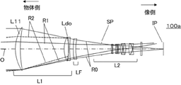
次に、図12を参照して、本発明の実施例5における光学系について説明する。図12は、回折光学素子Ldo(実施例1~4の回折光学素子に相当)を有する光学系100aの光路図である。
Next, the optical system according to the fifth embodiment of the present invention will be described with reference to FIG. FIG. 12 is an optical path diagram of an
本実施例の光学系100aは、焦点距離f=780mm、Fナンバー=5.8、最大像高Y=21.6mmである。光学系100は、物体側から像側へ順に、正の屈折力を有する第1レンズ群L1、フォーカス群LF、開口絞りSP、および、負の屈折力を有する第2レンズ群L2を有する。IPは像面である。光学系100aは、フォーカシングの際に、フォーカス群LFを像側に移動することにより、近距離物体への合焦が可能である。また、第1レンズ群L1は、レンズL11および回折光学素子Ldoを有する。
The
図12において、R0は軸上光束、R1は最大像高となる軸外光束、R2は回折光学素子Ldoに入射する画面外光束(最大像高光束以上の入射角度で入射する光束)をそれぞれ示す。光学系100aにおいて、回折光学素子Ldoを物体側のレンズL11から離れた位置に配置しているため、像高が図12中の上側にシフトして光束の入射角度が大きくなるにつれて、回折光学素子Ldoの図12中の下側に当たる光線の範囲が狭くなっている。このため、図3を参照して説明した光線2のように格子壁面に対して光軸Oと反対側から入射する光束が、回折光学素子Ldoよりも物体側のレンズL11により遮光されて回折光学素子Ldoの周辺部に入射しなくなる。すなわち光学系100aは、軸上光束の回折光学素子Ldoにおける最大有効径よりも最大像高光束の回折光学素子Ldoにおける最大有効径の方が小さい。このため、条件式(14)のように回折光学素子の周辺部の位相差を小さくしたことによる不要光の低減効果を効果的に得ることができる。
In FIG. 12, R0 indicates an on-axis luminous flux, R1 indicates an off-axis luminous flux having a maximum image height, and R2 indicates an off-screen luminous flux incident on the diffractive optical element Ldo (a luminous flux incident at an incident angle equal to or higher than the maximum image high luminous flux). .. In the
本実施例において、最も物体側の面から回折面までの距離をLd(mm)、最も物体側の面の光線有効径をE0(mm)とするとき、以下の条件式(20)を満足することが好ましい。 In this embodiment, the following conditional expression (20) is satisfied when the distance from the surface on the most object side to the diffraction surface is Ld (mm) and the effective diameter of the light beam on the surface on the most object side is E0 (mm). Is preferable.
0.300<E0/Ld<2.000 … (20)
条件式(20)の上限値を上回ると、回折光学素子Ldoよりも物体側のレンズL11による入射光束の遮蔽効果が小さくなり、不要光の低減効果が小さくなる。一方、条件式(20)の下限値を下回ると、回折光学素子Ldoによる収差補正効果が小さくなるため、光学系100aの諸収差の影響を受けることになる。
0.300 <E0 / Ld <2.000 ... (20)
When the upper limit of the conditional expression (20) is exceeded, the shielding effect of the incident light beam by the lens L11 on the object side becomes smaller than that of the diffractive optical element Ldo, and the effect of reducing unnecessary light becomes smaller. On the other hand, if it is less than the lower limit of the conditional expression (20), the aberration correction effect of the diffractive optical element Ldo becomes small, so that it is affected by various aberrations of the
また、本実施例の回折光学素子Ldoは、開口絞りSPよりも物体側に配置されることが好ましい。開口絞りSPよりも像側に回折光学素子Ldoを配置すると、画面外光束が回折光学素子Ldoに入射しにくくなる。このため、回折光学素子Ldoの周辺部における、壁面部の位相差を小さくしても十分な不要光の低減効果が得られにくい。また不要光の低減効果が得られた場合でも、効果が得られる画角が一部の画角のみとなり、好ましくない。 Further, it is preferable that the diffractive optical element Ldo of this embodiment is arranged closer to the object than the aperture stop SP. When the diffractive optical element Ldo is arranged on the image side of the aperture stop SP, the extrascreen light flux is less likely to be incident on the diffractive optical element Ldo. Therefore, even if the phase difference of the wall surface portion in the peripheral portion of the diffractive optical element Ldo is reduced, it is difficult to obtain a sufficient effect of reducing unnecessary light. Further, even when the effect of reducing unnecessary light is obtained, the angle of view from which the effect can be obtained is only a part of the angle of view, which is not preferable.
次に、図13を参照して、本発明の実施例6における光学系について説明する。図12は、回折光学素子Ldo(前述の各実施例の回折光学素子に相当)を有する光学系100bの光路図である。
Next, the optical system according to the sixth embodiment of the present invention will be described with reference to FIG. FIG. 12 is an optical path diagram of an
本実施例の光学系100bは、焦点距離f=196mm、Fナンバー=2.05、最大像高Y=21.6mmである。光学系100bは、物体側から像側へ順に、正の屈折力を有する第1レンズ群L1、フォーカス群LF、開口絞りSP、および、正の屈折力を有する第2レンズ群L2を有する。IPは像面である。光学系100bは、フォーカシングの際に、フォーカス群LFを像側に移動することにより、近距離物体への合焦が可能である。また、第1レンズ群L1は、レンズL11、および、回折光学素子Ldo(実施例1~4の回折光学素子に相当)を有する。
The
図13において、R0は軸上光束、R1は最大像高となる軸外光束をそれぞれ示す。光学系100bにおいて、回折光学素子Ldoを物体側のレンズL11から離れた位置に配置しているため、像高が図13中の上側にシフトして光束の入射角度が大きくなるにつれて、回折光学素子Ldoの図13中の下側に当たる光線の範囲が狭くなっている。このため、図3を参照して説明した光線2のように格子壁面に対して光軸Oと反対側から入射する光束が、回折光学素子Ldoよりも物体側のレンズL11により遮光されて回折光学素子Ldoの周辺部に入射しなくなる。回折光学素子の周辺部の位相差を小さくしたことによる不要光の低減効果を効果的に得ることができる。
In FIG. 13, R0 indicates an on-axis luminous flux, and R1 indicates an off-axis luminous flux having a maximum image height. In the
表2は、実施例5および実施例6の光学系100a、100bの各条件式に対応する値を示す。
Table 2 shows the values corresponding to the conditional expressions of the

なお実施例5および実施例6において、光学系100a、100bには1つの回折光学素子Ldoが配置されているが、これに限定されるものではなく、光学系100a、100bに複数の回折光学素子Ldoを配置してもよい。
In Examples 5 and 6, one diffractive optical element Ldo is arranged in the
次に、図14を参照して、本発明の実施例7における双眼鏡の観察光学系について説明する。図14は、観察光学系110の構成図である。
Next, the observation optical system of the binoculars according to the seventh embodiment of the present invention will be described with reference to FIG. FIG. 14 is a block diagram of the observation
図14において、103は結像面、104は対物レンズ、105は倒立像を正立させるためのプリズム、106は接眼レンズ、107は瞳面である。対物レンズ104は、レンズL11および回折光学素子Ldo(実施例1~4の回折光学素子に相当)を有する。回折光学素子Ldoは、対物レンズ104の結像面103での色収差等を補正する目的で設けられている。観察光学系110は、実施例1~4にて説明したように、回折効率特性が従来に比べて大幅に改善されているため、フレア光が少なく低周波数での解像力も高く、高い光学性能を有する。なお本実施例では、平板ガラス面に回折光学素子Ldoを設けているが、本発明はこれに限定されるものではなく、回折光学素子Ldoをレンズの凹面又は凸面上に設けてもよい。また、観察光学系110に複数の回折光学素子Ldoを配置してもよい。
In FIG. 14, 103 is an image plane, 104 is an objective lens, 105 is a prism for erecting an inverted image, 106 is an eyepiece, and 107 is a pupil plane. The
また本実施例では、対物レンズ104に回折光学素子Ldoを設けているが、これに限定されるものではなく、プリズム105の表面や接眼レンズ106内に開設光学素子Ldoを設けることもでき、この場合にも前述と同様の効果が得られる。ただし、回折光学素子Ldoを結像面103よりも物体側に設けることにより、対物レンズ104における色収差低減効果がある。このため、肉眼の観察系の場合、少なくとも対物レンズ104に回折光学素子Ldoを設けることが好ましい。なお本実施例では、双眼鏡の観察光学系110について説明したが、回折光学素子Ldoは、地上望遠鏡や天体観測用望遠鏡等の観察光学系にも適用可能である。また回折光学素子Ldoは、レンズシャッターカメラやビデオカメラなどの光学式ファインダにも適用可能である。これらの場合にも、前述と同様の効果が得られる。
Further, in this embodiment, the diffractive optical element Ldo is provided on the
次に、図15を参照して、本発明の実施例8における撮像装置について説明する。図15は、撮像装置120の概略図である。撮像装置120は、実施例1~4の回折光学素子を有する光学系を撮像光学系として用いたデジタルスチルカメラである。
Next, the image pickup apparatus according to the eighth embodiment of the present invention will be described with reference to FIG. FIG. 15 is a schematic view of the
図15において、125はカメラ本体、121は撮像光学系である。122は、カメラ本体125に内蔵され、撮像光学系121により形成された被写体像(光学像)を受光するCCDセンサやCMOSセンサ等の撮像素子(光電変換素子)である。123は撮像素子122によって光電変換された被写体像に対応する情報を記録するメモリ、124は液晶ディスプレイパネル等により構成され、撮像素子122上に形成された被写体像を観察するためのファインダである。このように各実施例の回折光学素子を備えた撮像光学系を用いることにより、フレアやゴーストが少ない、高い光学性能を有する撮像装置を実現することができる。
In FIG. 15, 125 is a camera body and 121 is an imaging optical system.
各実施例によれば、簡素な構成の回折光学素子において可視域全域で高い回折効率を得ると共に、設計入射光束とは異なる斜入射光束が回折光学素子に入射したときの、不要光の低減効果が場所ごとに最適化された回折光学素子を得ることができる。また、回折光学素子を光学系中に用いることにより、色収差等の諸収差やフレアが良好に低減された光学系を得ることができる。このため各実施例によれば、径方向の位置に応じて膜の特性を適切に設定することにより光学性能を向上させた回折光学素子、光学系、および、撮像装置を提供することができる。 According to each embodiment, a diffractive optical element having a simple structure can obtain high diffraction efficiency over the entire visible range, and can reduce unnecessary light when an oblique incident light beam different from the design incident light beam is incident on the diffractive optical element. It is possible to obtain a diffractive optical element optimized for each location. Further, by using the diffractive optical element in the optical system, it is possible to obtain an optical system in which various aberrations such as chromatic aberration and flare are satisfactorily reduced. Therefore, according to each embodiment, it is possible to provide a diffractive optical element, an optical system, and an image pickup apparatus having improved optical performance by appropriately setting the characteristics of the film according to the position in the radial direction.
以上、本発明の好ましい実施例について説明したが、本発明はこれらの実施例に限定されず、その要旨の範囲内で種々の変形及び変更が可能である。 Although the preferred embodiments of the present invention have been described above, the present invention is not limited to these examples, and various modifications and modifications can be made within the scope of the gist thereof.
1 回折光学素子
8 第1の回折格子
9 第2の回折格子
10 誘電体薄膜(薄膜)
1 Diffractive
Claims (11)
第2の格子面及び第2の格子壁面の夫々を複数備えた第2の回折格子と、を有し、
前記複数の第1の格子壁面の夫々と前記複数の第2の格子壁面の夫々は、薄膜を介して互いに密着しており、
設計波長λd(nm)において、前記第1及び第2の回折格子の屈折率をそれぞれn1及びn2、有効径内の第m輪帯(m=1、2、…)における前記薄膜の屈折率及び膜厚(nm)をそれぞれnhm及びdm、該屈折率nhmの平均値をnha、有効径内の前記薄膜と前記第1の回折格子との位相差をPm=(nhm-n1)×dm/λd、該Pmの最大値をPmax、前記位相差Pmのうち最も周辺側の前記薄膜と前記第1の回折格子との位相差をPe、前記位相差Pmのうち最も周辺側ではない少なくとも一つの輪帯における前記薄膜と前記第1の回折格子との間の位相差をPmaとし、前記第m輪帯における前記薄膜の屈折率及び前記膜厚は均一であるとするとき、
n2<n1<nha
-0.500<Pe/Pmax<0.700
0.013<Pma<0.035
なる条件式を満足することを特徴とする回折光学素子。 A first diffraction grating having a plurality of first lattice planes and a plurality of first lattice wall surfaces,
It has a second diffraction grating having a plurality of second lattice planes and a plurality of second lattice wall surfaces, respectively.
Each of the plurality of first lattice wall surfaces and each of the plurality of second lattice wall surfaces are in close contact with each other via a thin film.
At the design wavelength λd (nm), the refractive indexes of the first and second diffraction gratings are n1 and n2, respectively, and the refractive index and the refractive index of the thin film in the mth ring zone (m = 1, 2, ...) Within the effective diameter. The film thickness (nm) is nhm and dm, the average value of the refractive index nhm is nha, and the phase difference between the thin film within the effective diameter and the first diffraction grating is Pm = (nhm-n1) × dm / λd. The maximum value of the Pm is Pmax, the phase difference between the thin film on the peripheral side of the phase difference Pm and the first diffraction grating is Pe, and at least one ring of the phase difference Pm that is not the peripheral side. When the phase difference between the thin film and the first diffraction grating in the band is Pma, and the refractive index and the film thickness of the thin film in the m ring band are uniform .
n2 <n1 <nha
-0.500 <Pe / Pmax <0.700
0.013 <Pma <0.035
A diffractive optical element characterized by satisfying the conditional expression.
0.013<Pcnt<0.035
なる条件式を満足することを特徴とする請求項1に記載の回折光学素子。 When the average value of the phase difference between the thin film and the first diffraction grating within the range of 20% to 60% of the effective diameter of the phase difference Pm is PCNT.
0.013 <Pct <0.035
The diffractive optical element according to claim 1, wherein the diffractive optical element satisfies the conditional expression.
なる条件式を満足することを特徴とする請求項1または2に記載の回折光学素子。 -0.015 <Pe <0.018
The diffractive optical element according to claim 1 or 2, wherein the diffractive optical element satisfies the conditional expression.
-0.005<Pedg<0.021
なる条件式を満足することを特徴とする請求項1乃至3の何れか一項に記載の回折光学素子。 When the average value of the phase difference between the thin film and the first diffraction grating within the range of 80% to 100% of the effective diameter of the phase difference Pm is Pedg.
-0.005 <Pedg <0.021
The diffractive optical element according to any one of claims 1 to 3, wherein the diffractive optical element satisfies the conditional expression.
0.000≦de/dmax<0.700
なる条件式を満足することを特徴とする請求項1乃至4の何れか一項に記載の回折光学素子。 When the maximum value of the film thickness dm is dmax and the film thickness of the thin film on the peripheral side of the film thickness dm is de.
0.000 ≤ de / dmax <0.700
The diffractive optical element according to any one of claims 1 to 4, wherein the diffractive optical element satisfies the conditional expression.
-0.500<ΔNe/ΔNmax<0.700
なる条件式を満足することを特徴とする請求項1乃至5の何れか一項に記載の回折光学素子。 When the maximum value of the difference between the refractive index nhm and the refractive index n1 is ΔNmax, and the difference between the refractive index of the thin film on the peripheral side of the refractive index nhm and the refractive index n1 is ΔNe.
-0.500 <ΔNe / ΔNmax <0.700
The diffractive optical element according to any one of claims 1 to 5, wherein the diffractive optical element satisfies the conditional expression.
0.300<E0/Ld<2.000
なる条件式を満足することを特徴とする請求項7に記載の光学系。 When the distance from the surface on the most object side to the diffraction surface of the diffractive optical element is Ld and the effective diameter of the surface on the most object side is E0,
0.300 <E0 / Ld <2.000
The optical system according to claim 7, wherein the optical system satisfies the conditional expression.
該光学系により形成された像を受光する撮像素子とを有することを特徴とする撮像装置。 The optical system according to any one of claims 7 to 10.
An image pickup device comprising an image pickup element that receives an image formed by the optical system.
Priority Applications (2)
| Application Number | Priority Date | Filing Date | Title |
|---|---|---|---|
| JP2017198312A JP7071085B2 (en) | 2017-10-12 | 2017-10-12 | Diffractive optical element, optical system, and image pickup device |
| US16/154,789 US10890698B2 (en) | 2017-10-12 | 2018-10-09 | Diffraction optical element, optical system, and imaging apparatus |
Applications Claiming Priority (1)
| Application Number | Priority Date | Filing Date | Title |
|---|---|---|---|
| JP2017198312A JP7071085B2 (en) | 2017-10-12 | 2017-10-12 | Diffractive optical element, optical system, and image pickup device |
Publications (3)
| Publication Number | Publication Date |
|---|---|
| JP2019074551A JP2019074551A (en) | 2019-05-16 |
| JP2019074551A5 JP2019074551A5 (en) | 2020-11-19 |
| JP7071085B2 true JP7071085B2 (en) | 2022-05-18 |
Family
ID=66096447
Family Applications (1)
| Application Number | Title | Priority Date | Filing Date |
|---|---|---|---|
| JP2017198312A Expired - Fee Related JP7071085B2 (en) | 2017-10-12 | 2017-10-12 | Diffractive optical element, optical system, and image pickup device |
Country Status (2)
| Country | Link |
|---|---|
| US (1) | US10890698B2 (en) |
| JP (1) | JP7071085B2 (en) |
Families Citing this family (6)
| Publication number | Priority date | Publication date | Assignee | Title |
|---|---|---|---|---|
| JP7581059B2 (en) | 2021-01-13 | 2024-11-12 | キヤノン株式会社 | Optical system and imaging device |
| US12276863B2 (en) | 2021-01-13 | 2025-04-15 | Canon Kabushiki Kaisha | Optical system and image pickup apparatus |
| JP2023132925A (en) | 2022-03-11 | 2023-09-22 | キヤノン株式会社 | Optical system and imaging device |
| CN115079322B (en) * | 2022-06-30 | 2024-03-12 | 歌尔光学科技有限公司 | Grating structure, processing method thereof, lens and head-mounted display device |
| JP2024106445A (en) * | 2023-01-27 | 2024-08-08 | キヤノン株式会社 | Diffractive optical element, optical system, imaging device, and display device |
| JP2024106462A (en) * | 2023-01-27 | 2024-08-08 | キヤノン株式会社 | Diffractive optical element, optical system, imaging device, and display device |
Citations (2)
| Publication number | Priority date | Publication date | Assignee | Title |
|---|---|---|---|---|
| JP2016218436A (en) | 2015-05-15 | 2016-12-22 | キヤノン株式会社 | Diffraction optical element, optical system, and optical instrument |
| US20170123208A1 (en) | 2015-10-29 | 2017-05-04 | Tuomas Vallius | Diffractive optical element with uncoupled grating structures |
Family Cites Families (15)
| Publication number | Priority date | Publication date | Assignee | Title |
|---|---|---|---|---|
| US6650477B2 (en) * | 2000-06-07 | 2003-11-18 | Canon Kabushiki Kaisha | Diffractive optical element and optical apparatus having the same |
| JP4341332B2 (en) * | 2002-07-31 | 2009-10-07 | 旭硝子株式会社 | Optical head device |
| JP2004126394A (en) * | 2002-10-04 | 2004-04-22 | Nikon Corp | Diffractive optical element |
| JP4898379B2 (en) * | 2006-10-11 | 2012-03-14 | キヤノン株式会社 | Imaging optical system and imaging apparatus having the same |
| DE102007032371A1 (en) * | 2007-07-06 | 2009-01-15 | Carl Zeiss Laser Optics Gmbh | Method for coating an optical component for a laser arrangement |
| JP5132284B2 (en) * | 2007-12-03 | 2013-01-30 | キヤノン株式会社 | Diffractive optical element, optical system having the same, and optical instrument |
| WO2011099550A1 (en) | 2010-02-15 | 2011-08-18 | 株式会社ニコン | Optical element and optical system |
| JP2011242762A (en) * | 2010-04-23 | 2011-12-01 | Panasonic Corp | Diffraction optical element and optical instrument |
| JP5777353B2 (en) * | 2010-06-11 | 2015-09-09 | キヤノン株式会社 | Diffractive optical element, optical system, and optical instrument |
| JP5700984B2 (en) * | 2010-09-15 | 2015-04-15 | キヤノン株式会社 | Phase difference plate and projection type image display device |
| JP5787508B2 (en) * | 2010-11-11 | 2015-09-30 | キヤノン株式会社 | Diffractive optical element and optical system |
| CN103026273B (en) * | 2010-12-10 | 2014-12-03 | 松下电器产业株式会社 | Diffraction-grating lens, and imaging optical system and imaging device using said diffraction-grating lens |
| JP2013125259A (en) * | 2011-12-16 | 2013-06-24 | Canon Inc | Diffractive optical element, optical system, and optical apparatus |
| JP5885518B2 (en) * | 2012-01-30 | 2016-03-15 | キヤノン株式会社 | Imaging optical system and imaging apparatus having the same |
| JP2014170109A (en) | 2013-03-04 | 2014-09-18 | Canon Inc | Diffraction optical element, optical system and optical device |
-
2017
- 2017-10-12 JP JP2017198312A patent/JP7071085B2/en not_active Expired - Fee Related
-
2018
- 2018-10-09 US US16/154,789 patent/US10890698B2/en active Active
Patent Citations (2)
| Publication number | Priority date | Publication date | Assignee | Title |
|---|---|---|---|---|
| JP2016218436A (en) | 2015-05-15 | 2016-12-22 | キヤノン株式会社 | Diffraction optical element, optical system, and optical instrument |
| US20170123208A1 (en) | 2015-10-29 | 2017-05-04 | Tuomas Vallius | Diffractive optical element with uncoupled grating structures |
Also Published As
| Publication number | Publication date |
|---|---|
| US20190113663A1 (en) | 2019-04-18 |
| US10890698B2 (en) | 2021-01-12 |
| JP2019074551A (en) | 2019-05-16 |
Similar Documents
| Publication | Publication Date | Title |
|---|---|---|
| JP7071085B2 (en) | Diffractive optical element, optical system, and image pickup device | |
| US8223436B2 (en) | Rear attachment lens, imaging optical system and image pickup apparatus | |
| US8120852B2 (en) | Diffractive optical element, optical system, and optical apparatus | |
| JP5137432B2 (en) | Adherent two-layer type diffractive optical element and optical system and optical apparatus using the same | |
| JP5074790B2 (en) | Zoom lens and imaging apparatus having the same | |
| US9030750B2 (en) | Objective lens | |
| JPWO2011024258A1 (en) | Optical system and optical apparatus having the same | |
| WO2013141284A1 (en) | Infrared-ray optical system | |
| JP5258204B2 (en) | Diffractive optical element, optical system using the same, and optical instrument | |
| JP6971654B2 (en) | Optical system and an image pickup device having it | |
| JP4776988B2 (en) | Optical system and optical apparatus having the same | |
| KR20020071752A (en) | Diffracting optical element, and optical system and optical apparatus having the same | |
| JP2014109700A (en) | Image capturing optical system and image capturing device having the same | |
| JP3833754B2 (en) | Electronic camera with diffractive optical element | |
| JP2005215387A (en) | Optical system | |
| JPH10186223A (en) | Triplet lens | |
| WO2013161197A1 (en) | Zoom lens and optical equipment having same | |
| JP6192325B2 (en) | Imaging optical system and imaging apparatus having the same | |
| JP2018146879A (en) | Optical system and imaging apparatus having the same | |
| JP3467018B2 (en) | Optical system and optical equipment | |
| JP4817705B2 (en) | Optical system | |
| JPH1152233A (en) | Attachment lens and optical system equipped with it | |
| JP2015203790A (en) | Optical system and optical apparatus using the same | |
| JP4650715B2 (en) | Front teleconverter lens | |
| JP6991756B2 (en) | Imaging optical system and an imaging device having it |
Legal Events
| Date | Code | Title | Description |
|---|---|---|---|
| A521 | Request for written amendment filed |
Free format text: JAPANESE INTERMEDIATE CODE: A523 Effective date: 20201006 |
|
| A621 | Written request for application examination |
Free format text: JAPANESE INTERMEDIATE CODE: A621 Effective date: 20201006 |
|
| A977 | Report on retrieval |
Free format text: JAPANESE INTERMEDIATE CODE: A971007 Effective date: 20210730 |
|
| A131 | Notification of reasons for refusal |
Free format text: JAPANESE INTERMEDIATE CODE: A131 Effective date: 20210803 |
|
| A521 | Request for written amendment filed |
Free format text: JAPANESE INTERMEDIATE CODE: A523 Effective date: 20210916 |
|
| A131 | Notification of reasons for refusal |
Free format text: JAPANESE INTERMEDIATE CODE: A131 Effective date: 20211130 |
|
| A521 | Request for written amendment filed |
Free format text: JAPANESE INTERMEDIATE CODE: A523 Effective date: 20220121 |
|
| TRDD | Decision of grant or rejection written | ||
| A01 | Written decision to grant a patent or to grant a registration (utility model) |
Free format text: JAPANESE INTERMEDIATE CODE: A01 Effective date: 20220405 |
|
| A61 | First payment of annual fees (during grant procedure) |
Free format text: JAPANESE INTERMEDIATE CODE: A61 Effective date: 20220506 |
|
| R151 | Written notification of patent or utility model registration |
Ref document number: 7071085 Country of ref document: JP Free format text: JAPANESE INTERMEDIATE CODE: R151 |
|
| LAPS | Cancellation because of no payment of annual fees |