JP7068772B2 - Light emitting element - Google Patents
Light emitting element Download PDFInfo
- Publication number
- JP7068772B2 JP7068772B2 JP2017038861A JP2017038861A JP7068772B2 JP 7068772 B2 JP7068772 B2 JP 7068772B2 JP 2017038861 A JP2017038861 A JP 2017038861A JP 2017038861 A JP2017038861 A JP 2017038861A JP 7068772 B2 JP7068772 B2 JP 7068772B2
- Authority
- JP
- Japan
- Prior art keywords
- light emitting
- emitting element
- layer
- electrode
- current
- Prior art date
- Legal status (The legal status is an assumption and is not a legal conclusion. Google has not performed a legal analysis and makes no representation as to the accuracy of the status listed.)
- Active
Links
Images


Classifications
-
- H—ELECTRICITY
- H01—ELECTRIC ELEMENTS
- H01S—DEVICES USING THE PROCESS OF LIGHT AMPLIFICATION BY STIMULATED EMISSION OF RADIATION [LASER] TO AMPLIFY OR GENERATE LIGHT; DEVICES USING STIMULATED EMISSION OF ELECTROMAGNETIC RADIATION IN WAVE RANGES OTHER THAN OPTICAL
- H01S5/00—Semiconductor lasers
- H01S5/04—Processes or apparatus for excitation, e.g. pumping, e.g. by electron beams
- H01S5/042—Electrical excitation ; Circuits therefor
- H01S5/0421—Electrical excitation ; Circuits therefor characterised by the semiconducting contacting layers
-
- H—ELECTRICITY
- H01—ELECTRIC ELEMENTS
- H01L—SEMICONDUCTOR DEVICES NOT COVERED BY CLASS H10
- H01L33/00—Semiconductor devices with at least one potential-jump barrier or surface barrier specially adapted for light emission; Processes or apparatus specially adapted for the manufacture or treatment thereof or of parts thereof; Details thereof
- H01L33/48—Semiconductor devices with at least one potential-jump barrier or surface barrier specially adapted for light emission; Processes or apparatus specially adapted for the manufacture or treatment thereof or of parts thereof; Details thereof characterised by the semiconductor body packages
- H01L33/62—Arrangements for conducting electric current to or from the semiconductor body, e.g. lead-frames, wire-bonds or solder balls
-
- H—ELECTRICITY
- H01—ELECTRIC ELEMENTS
- H01S—DEVICES USING THE PROCESS OF LIGHT AMPLIFICATION BY STIMULATED EMISSION OF RADIATION [LASER] TO AMPLIFY OR GENERATE LIGHT; DEVICES USING STIMULATED EMISSION OF ELECTROMAGNETIC RADIATION IN WAVE RANGES OTHER THAN OPTICAL
- H01S5/00—Semiconductor lasers
- H01S5/10—Construction or shape of the optical resonator, e.g. extended or external cavity, coupled cavities, bent-guide, varying width, thickness or composition of the active region
- H01S5/12—Construction or shape of the optical resonator, e.g. extended or external cavity, coupled cavities, bent-guide, varying width, thickness or composition of the active region the resonator having a periodic structure, e.g. in distributed feedback [DFB] lasers
- H01S5/125—Distributed Bragg reflector [DBR] lasers
-
- H—ELECTRICITY
- H01—ELECTRIC ELEMENTS
- H01L—SEMICONDUCTOR DEVICES NOT COVERED BY CLASS H10
- H01L33/00—Semiconductor devices with at least one potential-jump barrier or surface barrier specially adapted for light emission; Processes or apparatus specially adapted for the manufacture or treatment thereof or of parts thereof; Details thereof
- H01L33/0004—Devices characterised by their operation
- H01L33/0045—Devices characterised by their operation the devices being superluminescent diodes
-
- H—ELECTRICITY
- H01—ELECTRIC ELEMENTS
- H01L—SEMICONDUCTOR DEVICES NOT COVERED BY CLASS H10
- H01L33/00—Semiconductor devices with at least one potential-jump barrier or surface barrier specially adapted for light emission; Processes or apparatus specially adapted for the manufacture or treatment thereof or of parts thereof; Details thereof
- H01L33/02—Semiconductor devices with at least one potential-jump barrier or surface barrier specially adapted for light emission; Processes or apparatus specially adapted for the manufacture or treatment thereof or of parts thereof; Details thereof characterised by the semiconductor bodies
- H01L33/10—Semiconductor devices with at least one potential-jump barrier or surface barrier specially adapted for light emission; Processes or apparatus specially adapted for the manufacture or treatment thereof or of parts thereof; Details thereof characterised by the semiconductor bodies with a light reflecting structure, e.g. semiconductor Bragg reflector
-
- H—ELECTRICITY
- H01—ELECTRIC ELEMENTS
- H01L—SEMICONDUCTOR DEVICES NOT COVERED BY CLASS H10
- H01L33/00—Semiconductor devices with at least one potential-jump barrier or surface barrier specially adapted for light emission; Processes or apparatus specially adapted for the manufacture or treatment thereof or of parts thereof; Details thereof
- H01L33/02—Semiconductor devices with at least one potential-jump barrier or surface barrier specially adapted for light emission; Processes or apparatus specially adapted for the manufacture or treatment thereof or of parts thereof; Details thereof characterised by the semiconductor bodies
- H01L33/14—Semiconductor devices with at least one potential-jump barrier or surface barrier specially adapted for light emission; Processes or apparatus specially adapted for the manufacture or treatment thereof or of parts thereof; Details thereof characterised by the semiconductor bodies with a carrier transport control structure, e.g. highly-doped semiconductor layer or current-blocking structure
- H01L33/145—Semiconductor devices with at least one potential-jump barrier or surface barrier specially adapted for light emission; Processes or apparatus specially adapted for the manufacture or treatment thereof or of parts thereof; Details thereof characterised by the semiconductor bodies with a carrier transport control structure, e.g. highly-doped semiconductor layer or current-blocking structure with a current-blocking structure
-
- H—ELECTRICITY
- H01—ELECTRIC ELEMENTS
- H01L—SEMICONDUCTOR DEVICES NOT COVERED BY CLASS H10
- H01L33/00—Semiconductor devices with at least one potential-jump barrier or surface barrier specially adapted for light emission; Processes or apparatus specially adapted for the manufacture or treatment thereof or of parts thereof; Details thereof
- H01L33/36—Semiconductor devices with at least one potential-jump barrier or surface barrier specially adapted for light emission; Processes or apparatus specially adapted for the manufacture or treatment thereof or of parts thereof; Details thereof characterised by the electrodes
-
- H—ELECTRICITY
- H01—ELECTRIC ELEMENTS
- H01S—DEVICES USING THE PROCESS OF LIGHT AMPLIFICATION BY STIMULATED EMISSION OF RADIATION [LASER] TO AMPLIFY OR GENERATE LIGHT; DEVICES USING STIMULATED EMISSION OF ELECTROMAGNETIC RADIATION IN WAVE RANGES OTHER THAN OPTICAL
- H01S5/00—Semiconductor lasers
- H01S5/04—Processes or apparatus for excitation, e.g. pumping, e.g. by electron beams
- H01S5/042—Electrical excitation ; Circuits therefor
- H01S5/0425—Electrodes, e.g. characterised by the structure
- H01S5/04252—Electrodes, e.g. characterised by the structure characterised by the material
- H01S5/04253—Electrodes, e.g. characterised by the structure characterised by the material having specific optical properties, e.g. transparent electrodes
-
- H—ELECTRICITY
- H01—ELECTRIC ELEMENTS
- H01S—DEVICES USING THE PROCESS OF LIGHT AMPLIFICATION BY STIMULATED EMISSION OF RADIATION [LASER] TO AMPLIFY OR GENERATE LIGHT; DEVICES USING STIMULATED EMISSION OF ELECTROMAGNETIC RADIATION IN WAVE RANGES OTHER THAN OPTICAL
- H01S5/00—Semiconductor lasers
- H01S5/04—Processes or apparatus for excitation, e.g. pumping, e.g. by electron beams
- H01S5/042—Electrical excitation ; Circuits therefor
- H01S5/0425—Electrodes, e.g. characterised by the structure
- H01S5/04254—Electrodes, e.g. characterised by the structure characterised by the shape
-
- H—ELECTRICITY
- H01—ELECTRIC ELEMENTS
- H01S—DEVICES USING THE PROCESS OF LIGHT AMPLIFICATION BY STIMULATED EMISSION OF RADIATION [LASER] TO AMPLIFY OR GENERATE LIGHT; DEVICES USING STIMULATED EMISSION OF ELECTROMAGNETIC RADIATION IN WAVE RANGES OTHER THAN OPTICAL
- H01S5/00—Semiconductor lasers
- H01S5/10—Construction or shape of the optical resonator, e.g. extended or external cavity, coupled cavities, bent-guide, varying width, thickness or composition of the active region
- H01S5/18—Surface-emitting [SE] lasers, e.g. having both horizontal and vertical cavities
- H01S5/183—Surface-emitting [SE] lasers, e.g. having both horizontal and vertical cavities having only vertical cavities, e.g. vertical cavity surface-emitting lasers [VCSEL]
- H01S5/18308—Surface-emitting [SE] lasers, e.g. having both horizontal and vertical cavities having only vertical cavities, e.g. vertical cavity surface-emitting lasers [VCSEL] having a special structure for lateral current or light confinement
- H01S5/18322—Position of the structure
-
- H—ELECTRICITY
- H01—ELECTRIC ELEMENTS
- H01S—DEVICES USING THE PROCESS OF LIGHT AMPLIFICATION BY STIMULATED EMISSION OF RADIATION [LASER] TO AMPLIFY OR GENERATE LIGHT; DEVICES USING STIMULATED EMISSION OF ELECTROMAGNETIC RADIATION IN WAVE RANGES OTHER THAN OPTICAL
- H01S5/00—Semiconductor lasers
- H01S5/10—Construction or shape of the optical resonator, e.g. extended or external cavity, coupled cavities, bent-guide, varying width, thickness or composition of the active region
- H01S5/18—Surface-emitting [SE] lasers, e.g. having both horizontal and vertical cavities
- H01S5/183—Surface-emitting [SE] lasers, e.g. having both horizontal and vertical cavities having only vertical cavities, e.g. vertical cavity surface-emitting lasers [VCSEL]
- H01S5/18344—Surface-emitting [SE] lasers, e.g. having both horizontal and vertical cavities having only vertical cavities, e.g. vertical cavity surface-emitting lasers [VCSEL] characterized by the mesa, e.g. dimensions or shape of the mesa
-
- H—ELECTRICITY
- H01—ELECTRIC ELEMENTS
- H01S—DEVICES USING THE PROCESS OF LIGHT AMPLIFICATION BY STIMULATED EMISSION OF RADIATION [LASER] TO AMPLIFY OR GENERATE LIGHT; DEVICES USING STIMULATED EMISSION OF ELECTROMAGNETIC RADIATION IN WAVE RANGES OTHER THAN OPTICAL
- H01S5/00—Semiconductor lasers
- H01S5/10—Construction or shape of the optical resonator, e.g. extended or external cavity, coupled cavities, bent-guide, varying width, thickness or composition of the active region
- H01S5/18—Surface-emitting [SE] lasers, e.g. having both horizontal and vertical cavities
- H01S5/183—Surface-emitting [SE] lasers, e.g. having both horizontal and vertical cavities having only vertical cavities, e.g. vertical cavity surface-emitting lasers [VCSEL]
- H01S5/18386—Details of the emission surface for influencing the near- or far-field, e.g. a grating on the surface
- H01S5/18394—Apertures, e.g. defined by the shape of the upper electrode
-
- H—ELECTRICITY
- H01—ELECTRIC ELEMENTS
- H01S—DEVICES USING THE PROCESS OF LIGHT AMPLIFICATION BY STIMULATED EMISSION OF RADIATION [LASER] TO AMPLIFY OR GENERATE LIGHT; DEVICES USING STIMULATED EMISSION OF ELECTROMAGNETIC RADIATION IN WAVE RANGES OTHER THAN OPTICAL
- H01S5/00—Semiconductor lasers
- H01S5/10—Construction or shape of the optical resonator, e.g. extended or external cavity, coupled cavities, bent-guide, varying width, thickness or composition of the active region
- H01S5/18—Surface-emitting [SE] lasers, e.g. having both horizontal and vertical cavities
- H01S5/185—Surface-emitting [SE] lasers, e.g. having both horizontal and vertical cavities having only horizontal cavities, e.g. horizontal cavity surface-emitting lasers [HCSEL]
- H01S5/187—Surface-emitting [SE] lasers, e.g. having both horizontal and vertical cavities having only horizontal cavities, e.g. horizontal cavity surface-emitting lasers [HCSEL] using Bragg reflection
-
- H—ELECTRICITY
- H01—ELECTRIC ELEMENTS
- H01S—DEVICES USING THE PROCESS OF LIGHT AMPLIFICATION BY STIMULATED EMISSION OF RADIATION [LASER] TO AMPLIFY OR GENERATE LIGHT; DEVICES USING STIMULATED EMISSION OF ELECTROMAGNETIC RADIATION IN WAVE RANGES OTHER THAN OPTICAL
- H01S5/00—Semiconductor lasers
- H01S5/20—Structure or shape of the semiconductor body to guide the optical wave ; Confining structures perpendicular to the optical axis, e.g. index or gain guiding, stripe geometry, broad area lasers, gain tailoring, transverse or lateral reflectors, special cladding structures, MQW barrier reflection layers
- H01S5/22—Structure or shape of the semiconductor body to guide the optical wave ; Confining structures perpendicular to the optical axis, e.g. index or gain guiding, stripe geometry, broad area lasers, gain tailoring, transverse or lateral reflectors, special cladding structures, MQW barrier reflection layers having a ridge or stripe structure
- H01S5/2205—Structure or shape of the semiconductor body to guide the optical wave ; Confining structures perpendicular to the optical axis, e.g. index or gain guiding, stripe geometry, broad area lasers, gain tailoring, transverse or lateral reflectors, special cladding structures, MQW barrier reflection layers having a ridge or stripe structure comprising special burying or current confinement layers
- H01S5/2213—Structure or shape of the semiconductor body to guide the optical wave ; Confining structures perpendicular to the optical axis, e.g. index or gain guiding, stripe geometry, broad area lasers, gain tailoring, transverse or lateral reflectors, special cladding structures, MQW barrier reflection layers having a ridge or stripe structure comprising special burying or current confinement layers based on polyimide or resin
-
- H—ELECTRICITY
- H01—ELECTRIC ELEMENTS
- H01S—DEVICES USING THE PROCESS OF LIGHT AMPLIFICATION BY STIMULATED EMISSION OF RADIATION [LASER] TO AMPLIFY OR GENERATE LIGHT; DEVICES USING STIMULATED EMISSION OF ELECTROMAGNETIC RADIATION IN WAVE RANGES OTHER THAN OPTICAL
- H01S5/00—Semiconductor lasers
- H01S5/20—Structure or shape of the semiconductor body to guide the optical wave ; Confining structures perpendicular to the optical axis, e.g. index or gain guiding, stripe geometry, broad area lasers, gain tailoring, transverse or lateral reflectors, special cladding structures, MQW barrier reflection layers
- H01S5/22—Structure or shape of the semiconductor body to guide the optical wave ; Confining structures perpendicular to the optical axis, e.g. index or gain guiding, stripe geometry, broad area lasers, gain tailoring, transverse or lateral reflectors, special cladding structures, MQW barrier reflection layers having a ridge or stripe structure
- H01S5/2205—Structure or shape of the semiconductor body to guide the optical wave ; Confining structures perpendicular to the optical axis, e.g. index or gain guiding, stripe geometry, broad area lasers, gain tailoring, transverse or lateral reflectors, special cladding structures, MQW barrier reflection layers having a ridge or stripe structure comprising special burying or current confinement layers
- H01S5/2214—Structure or shape of the semiconductor body to guide the optical wave ; Confining structures perpendicular to the optical axis, e.g. index or gain guiding, stripe geometry, broad area lasers, gain tailoring, transverse or lateral reflectors, special cladding structures, MQW barrier reflection layers having a ridge or stripe structure comprising special burying or current confinement layers based on oxides or nitrides
- H01S5/2216—Structure or shape of the semiconductor body to guide the optical wave ; Confining structures perpendicular to the optical axis, e.g. index or gain guiding, stripe geometry, broad area lasers, gain tailoring, transverse or lateral reflectors, special cladding structures, MQW barrier reflection layers having a ridge or stripe structure comprising special burying or current confinement layers based on oxides or nitrides nitrides
-
- H—ELECTRICITY
- H01—ELECTRIC ELEMENTS
- H01S—DEVICES USING THE PROCESS OF LIGHT AMPLIFICATION BY STIMULATED EMISSION OF RADIATION [LASER] TO AMPLIFY OR GENERATE LIGHT; DEVICES USING STIMULATED EMISSION OF ELECTROMAGNETIC RADIATION IN WAVE RANGES OTHER THAN OPTICAL
- H01S5/00—Semiconductor lasers
- H01S5/30—Structure or shape of the active region; Materials used for the active region
- H01S5/34—Structure or shape of the active region; Materials used for the active region comprising quantum well or superlattice structures, e.g. single quantum well [SQW] lasers, multiple quantum well [MQW] lasers or graded index separate confinement heterostructure [GRINSCH] lasers
- H01S5/343—Structure or shape of the active region; Materials used for the active region comprising quantum well or superlattice structures, e.g. single quantum well [SQW] lasers, multiple quantum well [MQW] lasers or graded index separate confinement heterostructure [GRINSCH] lasers in AIIIBV compounds, e.g. AlGaAs-laser, InP-based laser
-
- H—ELECTRICITY
- H01—ELECTRIC ELEMENTS
- H01L—SEMICONDUCTOR DEVICES NOT COVERED BY CLASS H10
- H01L2924/00—Indexing scheme for arrangements or methods for connecting or disconnecting semiconductor or solid-state bodies as covered by H01L24/00
- H01L2924/10—Details of semiconductor or other solid state devices to be connected
- H01L2924/11—Device type
- H01L2924/12—Passive devices, e.g. 2 terminal devices
- H01L2924/1204—Optical Diode
- H01L2924/12041—LED
-
- H—ELECTRICITY
- H01—ELECTRIC ELEMENTS
- H01L—SEMICONDUCTOR DEVICES NOT COVERED BY CLASS H10
- H01L2933/00—Details relating to devices covered by the group H01L33/00 but not provided for in its subgroups
- H01L2933/0008—Processes
- H01L2933/0033—Processes relating to semiconductor body packages
- H01L2933/0066—Processes relating to semiconductor body packages relating to arrangements for conducting electric current to or from the semiconductor body
-
- H—ELECTRICITY
- H01—ELECTRIC ELEMENTS
- H01S—DEVICES USING THE PROCESS OF LIGHT AMPLIFICATION BY STIMULATED EMISSION OF RADIATION [LASER] TO AMPLIFY OR GENERATE LIGHT; DEVICES USING STIMULATED EMISSION OF ELECTROMAGNETIC RADIATION IN WAVE RANGES OTHER THAN OPTICAL
- H01S2301/00—Functional characteristics
- H01S2301/18—Semiconductor lasers with special structural design for influencing the near- or far-field
-
- H—ELECTRICITY
- H01—ELECTRIC ELEMENTS
- H01S—DEVICES USING THE PROCESS OF LIGHT AMPLIFICATION BY STIMULATED EMISSION OF RADIATION [LASER] TO AMPLIFY OR GENERATE LIGHT; DEVICES USING STIMULATED EMISSION OF ELECTROMAGNETIC RADIATION IN WAVE RANGES OTHER THAN OPTICAL
- H01S5/00—Semiconductor lasers
- H01S5/02—Structural details or components not essential to laser action
- H01S5/022—Mountings; Housings
- H01S5/0233—Mounting configuration of laser chips
- H01S5/02345—Wire-bonding
-
- H—ELECTRICITY
- H01—ELECTRIC ELEMENTS
- H01S—DEVICES USING THE PROCESS OF LIGHT AMPLIFICATION BY STIMULATED EMISSION OF RADIATION [LASER] TO AMPLIFY OR GENERATE LIGHT; DEVICES USING STIMULATED EMISSION OF ELECTROMAGNETIC RADIATION IN WAVE RANGES OTHER THAN OPTICAL
- H01S5/00—Semiconductor lasers
- H01S5/02—Structural details or components not essential to laser action
- H01S5/026—Monolithically integrated components, e.g. waveguides, monitoring photo-detectors, drivers
-
- H—ELECTRICITY
- H01—ELECTRIC ELEMENTS
- H01S—DEVICES USING THE PROCESS OF LIGHT AMPLIFICATION BY STIMULATED EMISSION OF RADIATION [LASER] TO AMPLIFY OR GENERATE LIGHT; DEVICES USING STIMULATED EMISSION OF ELECTROMAGNETIC RADIATION IN WAVE RANGES OTHER THAN OPTICAL
- H01S5/00—Semiconductor lasers
- H01S5/02—Structural details or components not essential to laser action
- H01S5/028—Coatings ; Treatment of the laser facets, e.g. etching, passivation layers or reflecting layers
- H01S5/0282—Passivation layers or treatments
- H01S5/0283—Optically inactive coating on the facet, e.g. half-wave coating
-
- H—ELECTRICITY
- H01—ELECTRIC ELEMENTS
- H01S—DEVICES USING THE PROCESS OF LIGHT AMPLIFICATION BY STIMULATED EMISSION OF RADIATION [LASER] TO AMPLIFY OR GENERATE LIGHT; DEVICES USING STIMULATED EMISSION OF ELECTROMAGNETIC RADIATION IN WAVE RANGES OTHER THAN OPTICAL
- H01S5/00—Semiconductor lasers
- H01S5/02—Structural details or components not essential to laser action
- H01S5/028—Coatings ; Treatment of the laser facets, e.g. etching, passivation layers or reflecting layers
- H01S5/0286—Coatings with a reflectivity that is not constant over the facets, e.g. apertures
-
- H—ELECTRICITY
- H01—ELECTRIC ELEMENTS
- H01S—DEVICES USING THE PROCESS OF LIGHT AMPLIFICATION BY STIMULATED EMISSION OF RADIATION [LASER] TO AMPLIFY OR GENERATE LIGHT; DEVICES USING STIMULATED EMISSION OF ELECTROMAGNETIC RADIATION IN WAVE RANGES OTHER THAN OPTICAL
- H01S5/00—Semiconductor lasers
- H01S5/10—Construction or shape of the optical resonator, e.g. extended or external cavity, coupled cavities, bent-guide, varying width, thickness or composition of the active region
- H01S5/18—Surface-emitting [SE] lasers, e.g. having both horizontal and vertical cavities
- H01S5/183—Surface-emitting [SE] lasers, e.g. having both horizontal and vertical cavities having only vertical cavities, e.g. vertical cavity surface-emitting lasers [VCSEL]
- H01S5/18308—Surface-emitting [SE] lasers, e.g. having both horizontal and vertical cavities having only vertical cavities, e.g. vertical cavity surface-emitting lasers [VCSEL] having a special structure for lateral current or light confinement
-
- H—ELECTRICITY
- H01—ELECTRIC ELEMENTS
- H01S—DEVICES USING THE PROCESS OF LIGHT AMPLIFICATION BY STIMULATED EMISSION OF RADIATION [LASER] TO AMPLIFY OR GENERATE LIGHT; DEVICES USING STIMULATED EMISSION OF ELECTROMAGNETIC RADIATION IN WAVE RANGES OTHER THAN OPTICAL
- H01S5/00—Semiconductor lasers
- H01S5/10—Construction or shape of the optical resonator, e.g. extended or external cavity, coupled cavities, bent-guide, varying width, thickness or composition of the active region
- H01S5/18—Surface-emitting [SE] lasers, e.g. having both horizontal and vertical cavities
- H01S5/183—Surface-emitting [SE] lasers, e.g. having both horizontal and vertical cavities having only vertical cavities, e.g. vertical cavity surface-emitting lasers [VCSEL]
- H01S5/18344—Surface-emitting [SE] lasers, e.g. having both horizontal and vertical cavities having only vertical cavities, e.g. vertical cavity surface-emitting lasers [VCSEL] characterized by the mesa, e.g. dimensions or shape of the mesa
- H01S5/1835—Non-circular mesa
-
- H—ELECTRICITY
- H01—ELECTRIC ELEMENTS
- H01S—DEVICES USING THE PROCESS OF LIGHT AMPLIFICATION BY STIMULATED EMISSION OF RADIATION [LASER] TO AMPLIFY OR GENERATE LIGHT; DEVICES USING STIMULATED EMISSION OF ELECTROMAGNETIC RADIATION IN WAVE RANGES OTHER THAN OPTICAL
- H01S5/00—Semiconductor lasers
- H01S5/10—Construction or shape of the optical resonator, e.g. extended or external cavity, coupled cavities, bent-guide, varying width, thickness or composition of the active region
- H01S5/18—Surface-emitting [SE] lasers, e.g. having both horizontal and vertical cavities
- H01S5/183—Surface-emitting [SE] lasers, e.g. having both horizontal and vertical cavities having only vertical cavities, e.g. vertical cavity surface-emitting lasers [VCSEL]
- H01S5/18386—Details of the emission surface for influencing the near- or far-field, e.g. a grating on the surface
- H01S5/18391—Aperiodic structuring to influence the near- or far-field distribution
-
- H—ELECTRICITY
- H01—ELECTRIC ELEMENTS
- H01S—DEVICES USING THE PROCESS OF LIGHT AMPLIFICATION BY STIMULATED EMISSION OF RADIATION [LASER] TO AMPLIFY OR GENERATE LIGHT; DEVICES USING STIMULATED EMISSION OF ELECTROMAGNETIC RADIATION IN WAVE RANGES OTHER THAN OPTICAL
- H01S5/00—Semiconductor lasers
- H01S5/40—Arrangement of two or more semiconductor lasers, not provided for in groups H01S5/02 - H01S5/30
- H01S5/42—Arrays of surface emitting lasers
- H01S5/423—Arrays of surface emitting lasers having a vertical cavity
Description
本発明は、発光素子に関し、特にレーザ及び発光ダイオード特性を有する発光素子に関する。 The present invention relates to a light emitting device, particularly to a light emitting device having laser and light emitting diode characteristics.
発光ダイオードは、固体照明光源に幅広く使われている。従来の白熱電球及び蛍光灯に比べて、発光ダイオードは低消費電力及び長寿命などの利点を有するため、発光ダイオードは、次第に従来の光源に取って代わり、交通標識、バックライトモジュール、街路照明、医療機器などの各種の分野に応用されている。 Light emitting diodes are widely used in solid-state lighting sources. Since light emitting diodes have advantages such as low power consumption and long life compared to conventional incandescent lamps and fluorescent lamps, light emitting diodes gradually replace conventional light sources, such as traffic signs, backlight modules, street lighting, etc. It is applied to various fields such as medical equipment.
図24は従来の垂直キャビティ面発光レーザ(VCSEL:Vertical-Cavity Surface-Emitting Laser)の断面図である。垂直キャビティ面発光レーザは、活性領域に垂直な方向にコヒーレント光を発することができる。VCSELは、基板300、及び基板300上に位置し、且つ活性領域230を挟む一対のDBR(Distributed Bragg Reflector:分布ブラッグ反射鏡)スタック200、210を有する構造を含み、活性領域230は、電子と正孔とが結合して光を発生させる場所である。活性領域230に電流を注入して光を発生させるために、第1電極240及び第2電極250を設け、光はVCSELの上面に位置する開孔(aperture)から逃げる。
FIG. 24 is a cross-sectional view of a conventional vertical cavity surface emitting laser (VCSEL: Vertical-cavity Surface-Emitting Laser). The vertical cavity surface emitting laser can emit coherent light in a direction perpendicular to the active region. The VCSEL comprises a structure having a
DBRスタック210において、垂直キャビティ面発光レーザはアンダーカット260を有することができる。図24の例では、アンダーカット260は、DBRスタック210における1つの層の周辺部を選択的に除去することで隙間を形成し、隙間に空気が入ることができ、空気の導電率が半導体材料の導電率よりも明らかに低いため、DBRスタック210における他の層の導電率に比べて、DBRスタック210に形成されたアンダーカット260は比較的に低い導電率を有する。
In the
本発明は発光素子を提供する。 The present invention provides a light emitting device.
放射を放出可能な発光素子であって、基板と、前記基板の上に位置し、第1DBR(Distributed Bragg Reflector:分布ブラッグ反射鏡)スタック、発光スタック、第2DBRスタック及びコンタクト層を順次含むエピタキシャル構造と、電極と、前記コンタクト層と前記電極との間に位置する電流ブロック層と、前記電流ブロック層の中に形成された第1開口と、前記電極の中に形成され、且つ前記第1開口の内に位置する第2開口と、を含み、前記電極の一部は、前記第1開口の中に埋め込まれ、且つ前記コンタクト層と接触し、前記発光素子は、前記第2DBRスタックにおいて、酸化層及びイオン注入層を有しない、発光素子を開示する。 An epitaxial structure that is a light emitting element capable of emitting radiation and is located on the substrate and sequentially includes a first DBR (Distributed Bragg Reflector) stack, a light emitting stack, a second DBR stack, and a contact layer. The electrode, the current block layer located between the contact layer and the electrode, the first opening formed in the current block layer, and the first opening formed in the electrode. A part of the electrode is embedded in the first opening and in contact with the contact layer, and the light emitting element is oxidized in the second DBR stack. A light emitting element having no layer and an ion injection layer is disclosed.
以下は図面を参照しながら本発明の概念を説明し、図面又は説明では、類似又は同一の部分について同一の符号を使用し、図面において、素子の形状又は厚さを拡大、或いは縮小してもよい。なお、図面に示せず、或いは明細書に説明されていない素子は、当業者にとって自明な形であってもよい。 The following describes the concept of the present invention with reference to the drawings, in which the same reference numerals are used for similar or identical parts in the drawings or description, and the shape or thickness of the element may be enlarged or reduced in the drawings. good. It should be noted that elements not shown in the drawings or not described in the specification may be of a form obvious to those skilled in the art.
本開示内容では、特段の説明がない限り、通式AlGaAsはAlxGa(1-x)Asを表し、0≦x≦1、通式AlInPはAlxIn(1-x)Pを表し、0≦x≦1、通式AlGaInPは(AlyGa(1-y))1-xInxPを表し、0≦x≦1、0≦y≦1、通式AlGaNはAlxGa(1-x)Nを表し、0≦x≦1、通式AlAsSbはAlAs(1-x)Sbxを表し、0≦x≦1、通式InGaPはInxGa1-xPを表し、0≦x≦1。元素の含有量を調整することで異なる目的を達成でき、例えばエネルギーレベル又は主発光波長を調整する。 In the present disclosure, unless otherwise specified, the general AlGaAs represents Al x Ga (1-x) As, 0 ≦ x ≦ 1, and the general AlInP represents Al x In (1-x) P. 0 ≦ x ≦ 1, general AlGaInP represents (Al y Ga (1-y) ) 1-x In x P, 0 ≦ x ≦ 1, 0 ≦ y ≦ 1, general AlGaN is Al x Ga (1) -X ) N, 0 ≦ x ≦ 1, general AlAsSb represents AlAs (1-x) Sb x , 0 ≦ x ≦ 1, general InGaP represents In x Ga 1-x P, 0 ≦ x ≦ 1. Different objectives can be achieved by adjusting the element content, for example adjusting the energy level or the main emission wavelength.
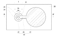
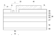
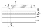
図1Aは本開示内容の第1実施例の発光素子の平面図である。図1Bは本開示内容の第1実施例の発光素子の図1AのA-A’線に沿う断面図である。本実施例では、発光素子は、基板10、基板10の上に位置するエピタキシャル構造20、電流ブロック層30、第1電極40及び第2電極50を含む。エピタキシャル構造20は、第1DBR(Distributed Bragg Reflector:分布ブラッグ反射鏡)スタック21、発光スタック22、第2DBRスタック23及びコンタクト層24を順次含む。第1DBRスタック21の導電形態は第2DBRスタック23の導電形態と異なる。本実施例では、第1DBRスタック21はn型であり、第2DBRスタック23はp型である。電流ブロック層30は、コンタクト層24と第1電極40との間に位置する。第1開口31は電流ブロック層30の中に形成され、コンタクト層24を露出させる。第1開口31は第1最大幅W1を有する。第1電極40の一部は、第1開口31の中に埋め込まれ、且つコンタクト層24と直接接触する。第2開口25は第1電極40の中に形成され、コンタクト層24を露出させ、第2開口25は、第1最大幅W1よりも小さい第2最大幅W2を有する。第2電極50は、基板10のエピタキシャル構造20に対向する側に位置する。発光素子は放射Rを放出でき、放射Rは600ナノメートル(nm)~1600ナノメートル(nm)のピーク波長を有し、好ましくは、ピーク波長は830ナノメートル~1000ナノメートルである。
FIG. 1A is a plan view of a light emitting device according to the first embodiment of the present disclosure. FIG. 1B is a cross-sectional view taken along the line AA'of FIG. 1A of the light emitting device of the first embodiment of the present disclosure. In this embodiment, the light emitting device includes a
図1Bに示すように、本実施例では、基板10の幅、エピタキシャル構造20の幅及び電流ブロック層30の幅は略同じである。本実施例では、第1開口31の形状は円形であり、第1最大幅W1は円形の直径である。第1開口31の形状は、本実施例に限定されず、楕円形、矩形、正方形、菱形又は他の任意の形状であってもよい。第1最大幅W1は20ミクロン(μm)~50ミクロンであってもよいが、これに限定されない。電流ブロック層30は、アルミニウム酸化物(AlOx)、シリコン酸化物(SiOx)、シリコン酸窒化物(SiOxNy)、シリコン窒化物(SixNy)、エポキシ樹脂(epoxy)、ポリイミド(polyimide)、ペルフルオロシクロブタン(perfluorocyclobutane)、ベンゾシクロブテン(BCB:benzocyclobutene)又はシリコーン(silicone)を含む絶縁材料を含む。好ましくは、発光スタックにより放出された放射は、実質的に電流ブロック層30を透過できる。電流ブロック層30は、100nmよりも大きい厚さを有し、好ましくは、2μmよりも小さく、より好ましくは、nλ/4に近く、或いは等しく、λは発光スタック22により放出された放射のピーク波長であり、nは奇数の正整数である。
As shown in FIG. 1B, in this embodiment, the width of the
本実施例では、第2開口25の形状は円形であり、第2最大幅W2は円形の直径である。第2開口25の形状は、本実施例に限定されず、楕円形、矩形、正方形、菱形又は他の任意の形状であってもよい。好ましくは、第2開口25の形状は、第1開口31の形状と略同じである。好ましくは、第1開口31と第2開口25は略同心円である。
In this embodiment, the shape of the
図1A及び図1Bに示すように、第1電極40は、連続的な層であり、リード線に接続するためのワイヤボンディング部41、電流を注入してエピタキシャル構造20を通過させるための電流注入部42、及びワイヤボンディング部41と電流注入部42とを接続するためのブリッジング部43を含む。ワイヤボンディング部41は電流ブロック層30上に位置する。電流注入部42は、第1開口31内に埋め込まれ、且つコンタクト層24と接触する。1つの態様では、第1開口25は電流注入部42内に形成されているため、電流注入部42は環状の形である。具体的には、本実施例では、図1A及び図1Bに示すように、電流注入部42の一部は電流ブロック層30の側壁と分離されているため、電流注入部42と電流ブロック層30の側壁との間に隙間が形成され、エピタキシャル構造20の一部を露出させる。本実施例の第1電極40は、電流ブロック層30の50%未満の表面積を覆う。電流ブロック層30のブリッジング部43とエピタキシャル構造20との間に位置する部分及びワイヤボンディング部41とエピタキシャル構造20との間に位置する部分は、電流がワイヤボンディング部41及びブリッジング部43からエピタキシャル構造20に直接流れることを防止するためのものである。
As shown in FIGS. 1A and 1B, the
本実施例では、発光素子は、第2DBRスタック23において、高抵抗構造を有しておらず、ここで、高抵抗構造は、第2DBRスタック23において第1電極40の直下に位置し、且つ第1電極40により覆われている層を意味し、第2DBR23において第1電極40の直下に位置し、且つ第1電極により覆われている他の層に比べて、相対的に低い導電率を有する。具体的には、高抵抗構造は、酸化層、イオン注入層又は図24に示すアンダーカットである。好ましくは、第2DBRスタック23の電流ブロック層30の直下に位置する部分及び/又は第1電極40の直下に位置する部分は酸化層、イオン注入層又はアンダーカットを有しない。即ち、第2DBRスタック23の第1開口31の直下に位置する部分の導電率は、全体から見ると、第2DBRスタック23の電流ブロック層30により覆われている部分の導電率に略同じである。
In this embodiment, the light emitting element does not have a high resistance structure in the
好ましくは、第2DBRスタック23は、実質的には、III-V族半導体材料、例えばAlGaAsからなるものである。第2DBRスタック23は、酸化物、例えば意図的に形成されたアルミナを有せず、ここで、アルミナはAlaObの実験式を有し、a及びbはゼロを除く自然数である。また、第2DBRスタック23は、任意の導電率を低減させるイオンを有せず、導電率を低減させるイオンは、第2DBRスタック23の一部の導電率を低減させ、且つ他の導電部分の第2DBR23スタックの導電率に比べて3桁以上、好ましくは5桁以上だけ低減するように、意図的に形成されたものである。導電率を低減させるイオンは、アルゴン(Ar)イオン、ヘリウム(He)イオン又は水素(H)イオンを含む。第2DBRスタック23は、環境に存在する不可避なイオンを含む可能性があるが、不可避なイオンが第2DBRスタック23の導電率を実質的に変化させなく、例えば他の導電部分の第2DBRスタック23の導電率に比べて不可避なイオンが導電率を実質的に1桁以上だけ低減させることがないため、本開示内容では不可避なイオンを考慮すべきではない。1つの態様では、発光素子が第2DBRスタック23において図24に示すアンダーカットを有しないため、第2DBRスタック23の各層が実質的にIII-V族半導体材料からなり、且つ空気の隙間が第2DBRスタック23の何れの層にも存在しない。
Preferably, the
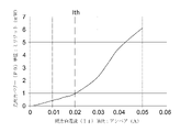
電流がエピタキシャル構造20に流入する際に、第1開口31における電流注入部42がエピタキシャル構造20のコンタクト層24と直接接触し、且つワイヤボンディング部41及びブリッジング部43が電流ブロック層30によりエピタキシャル構造20と分離し、且つ絶縁するため、電流は、主にエピタキシャル構造20の電流ブロック層30により覆われておらず、且つ電流注入部42と直接接触する部分を介して流れる。即ち、電流がエピタキシャル構造20に流入する際に、第2DBRスタック23の電流ブロック層30の直下に位置する部分の電流密度は、第2DBRスタック23の電流ブロック層により覆われていない部分の電流密度よりも遥かに低い。このため、エピタキシャル構造20の電流注入部42と直接接触し、且つ概ね第1開口31の直下に位置する部分は、放射Rを発生する放射放出領域Iとなる。放射Rは、第1開口により発光素子から逃げる。具体的には、エピタキシャル構造20の最上層、即ち本実施例のコンタクト層24は、エピタキシャル構造20のうち発光素子の制限後の電流を伝導する半導体層の1番目の層である。図2は本開示内容の第1実施例の発光素子の光出力パワー(optical output power、P0)と順方向電流(forward current、If)の関係曲線を示す図である。本実施例では、発光素子は、順方向電圧Vf、レーザ閾値電流Ith、及び飽和電流Isatを有する。発光素子は、順方向電圧Vfにおいて明らかな順方向電流を伝導し始め、例えば、本実施例では、明らかな順方向電流は5ミリアンペア(mA)である。レーザ閾値電流Ithは発光素子の放射放出領域により放出された放射の誘導放出(stimulated emission)が自然放出(spontaneous emission)を超えた場合の最小電流であるため、レーザ閾値電流Ithにおける放射はコヒーレントのものである。飽和電流Isatは、放射の出力が順方向電流の増加に伴って増加しない場合の電流である。発光素子が発光素子の順方向電圧Vfよりも大きい動作電圧Vop及びレーザ閾値電流Ithよりも小さい順方向電流で動作する場合、本開示内容の発光素子の放射放出領域Iにより放出された放射は非コヒーレント光である。好ましくは、発光素子が発光素子の順方向電圧Vfよりも大きい動作電圧Vop及びレーザ閾値電流Ithよりも小さい順方向電流で動作する場合、非コヒーレント光は60度よりも大きいファーフィールド角を有する。発光素子がレーザ閾値電流Ithより大きく、且つ飽和電流Isatよりも小さい順方向電流で動作する場合、発光素子の放射放出領域Iにより放出された放射Rは15度よりも小さいファーフィールド角を有するコヒーレント光である。具体的には、発光素子の順方向電流がレーザ閾値電流Ithに実質的に等しい場合、エピタキシャル構造20の非放射放出領域の電流密度は放射放出領域Iの電流密度よりも遥かに小さく、且つワイヤボンディング部41及びブリッジング部43がエピタキシャル構造20により放出された放射を遮蔽し、エピタキシャル構造20の非放射放出領域であり、且つ第1電極40により覆われていない領域は非コヒーレント光R1を放出する。
When the current flows into the
本実施例では、レーザ閾値電流Ithは約20ミリアンペアである。レーザ閾値電流Ith、飽和電流Isat及びレーザ閾値電流Ithと飽和電流Isatの差は、異なる応用要求に応じて第1開口31の第1最大幅W1で調整されてもよい。例えば、高いレーザ閾値電流Ith、高い飽和電流Isat及び高いレーザ閾値電流Ithと飽和電流Isatの差が必要となる場合、第1最大幅W1が大きい方が好ましい。具体的には、レーザ閾値電流Ithと第1最大幅W1は次の式を満たす。
In this embodiment, the laser threshold current Ith is about 20mA. The difference between the laser threshold current It, the saturation current Ist , and the laser threshold current It and the saturation current Isat may be adjusted by the first maximum width W1 of the
0.4W1(μm)-7≦Ith(ミリアンペア)≦0.4W1(μm)+7
表1は、異なる順方向電流の場合の発光素子の放射のファーフィールド角を示している。光束の発散度を明確に説明するために、本開示内容のファーフィールド角は半ビーム幅の発散角である。
0.4W 1 (μm) -7 ≤ If (milliampere) ≤ 0.4W 1 (μm) +7
Table 1 shows the farfield angle of radiation of the light emitting device for different forward currents. In order to clearly explain the divergence of the luminous flux, the farfield angle of the present disclosure is a divergence angle of a half beam width.

表1から分かるように、順方向電流がレーザ閾値電流Ithよりも高く、且つ飽和電流Isatよりも低い場合、放射のファーフィールド角は15度よりも小さく、好ましくは、5度~15度であり、より好ましくは、5度~13度である。
As can be seen from Table 1, when the forward current is higher than the laser threshold current It and lower than the saturation current Isat , the farfield angle of radiation is less than 15 degrees, preferably 5 degrees to 15 degrees. It is more preferably 5 to 13 degrees.
本開示内容では、発光素子が第2DBRスタック23において酸化層及びイオン注入層を含む高抵抗構造を有しないが、電流ブロック層30及び第1電極を含むことで、エピタキシャル構造20の最上層がエピタキシャル構造20の発光素子の制限後の電流を伝導する1番目の層となり、順方向電流がレーザ閾値電流Ithと飽和電流Isatとの間のものである場合、発光素子は15度よりも小さいファーフィールド角を有する。また、従来技術の発光素子が第2DBRスタック23において酸化層などの高抵抗構造を含み、正常の動作条件で、特に高い順方向電流の動作では、従来技術の発光素子は大きいファーフィールド角を有する。しかし、順方向電流がレーザ閾値電流Ithと飽和電流Isatとの間のものである場合、本開示内容の発光素子は15度よりも小さいファーフィールド角を有する。発光素子は、例えば近接センサ、ナイトビジョンシステム又は血液酸素検出器などのセンサに適用されてもよい。
In the present disclosure, the light emitting device does not have a high resistance structure including an oxide layer and an ion injection layer in the
図3A乃至図4Bは図1A及び図1Bに示す発光素子の製造方法を示す図である。図3Bは本開示内容の図3AのA-A’線に沿う断面図である。図4Bは本開示内容の図4AのA-A’線に沿う断面図である。本方法は下記のステップを含む。 3A to 4B are diagrams showing a method of manufacturing the light emitting element shown in FIGS. 1A and 1B. FIG. 3B is a cross-sectional view taken along the line AA'of FIG. 3A of the present disclosure. FIG. 4B is a cross-sectional view taken along the line AA'of FIG. 4A of the present disclosure. The method includes the following steps.
a.図3A及び図3Bに示すように、基板10を提供する。
a. As shown in FIGS. 3A and 3B, the
b.エピタキシャル成長により基板10の上にエピタキシャル構造20を形成する。
b. The
c.任意の適切な方法、例えばスパッタリング又は蒸着により、エピタキシャル構造20の上に電流ブロック層30を形成する。
c. The
d.フォトリソグラフィ・マスクにより電流ブロック層30をパターン化し、任意の適切な方法で第1開口31を形成してエピタキシャル構造20の一部を露出させる。
d. The
e.電流ブロック層30の上に金属層(図示せず)を形成し、図4A及び図4Bに示す第1開口31を覆う。
e. A metal layer (not shown) is formed on the
f.フォトリソグラフィ・マスクにより金属層をパターン化して第1電極40を形成し、第1電極は電流注入部42、ワイヤボンディング部41、及びワイヤボンディング部41と電流注入部42を接続させるブリッジング部43を含み、ワイヤボンディング部41及びブリッジング部43は電流ブロック層30の上に位置し、電流注入部42は第1開口31の中に埋め込まれ、第2開口25を電流注入部42内に形成してエピタキシャル構造20を露出させる。
f. A metal layer is patterned by a photolithographic mask to form a
g.任意の適切な方法により基板10のエピタキシャル構造20に対向する他方側に第2電極50を形成する。
g. The
h.ステップgにおいて形成された構造を切断し、図1A及び図1Bに示すそれぞれ形成された発光素子を取得する。 h. The structure formed in step g is cut to obtain the formed light emitting elements shown in FIGS. 1A and 1B, respectively.
本開示内容の方法は、第2DBRスタック23の導電率を低減させるステップ、例えば酸化領域の導電率、イオン注入領域の導電率又は図24に示すアンダーカットの導電率が第2DBRスタック23の処理領域以外の他部の導電率よりも低くするための、第2DBRスタック23のうち少なくとも1つの層を酸化する酸化ステップ、第2DBRスタック23のうち少なくとも1つの層において少なくとも導電率を低減させるイオンを注入するステップ、及び/又は第2DBRスタック23のうち少なくとも1つの層の周辺部を選択的にエッチングして図24に示すアンダーカットを形成するステップを含まない。酸化ステップ、イオン注入ステップ及び第2DBRスタック23のうち1つの層をエッチングするステップは、第2DBRスタック23の第1電極40の直下に位置する部分を略絶縁の領域に変換して第2DBRスタック23に高抵抗構造を形成するためのものである。本開示内容の方法は、パターン化プロセスにおいて、4種類以下の異なるフォトリソグラフィ・マスクを用いる。本実施例では、本方法は、パターン化プロセスにおいて、2種類の異なるフォトリソグラフィ・マスクを用いる。従って、本開示内容の発光素子の製造方法は簡単であり、且つ低コストの利点を有する。
In the method of the present disclosure, a step of reducing the conductivity of the
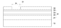
図5Aは本開示内容の第2実施例の発光素子の平面図である。図5Bは本開示内容の第1実施例の発光素子の図5AのA-A’線に沿う断面図である。本明細書では、特段の説明がない限り、同一の符号は、異なる図面において、本開示内容の全ての説明された同一又は略同一の構造、材料、材料組成及び/又は製造方法に対応する。本開示内容の第2実施例の発光素子は、第1実施例と略同一の構成を含み、相違点として、電流ブロック層30の幅はエピタキシャル構造20の幅よりも小さい。従って、発光素子の平面において、エピタキシャル構造20の周辺部は電流ブロック層30から露出している。また、第1電極40は第1実施例と異なる形状を有する。具体的には、第1電極40は、電流ブロック層30の第1開口31を囲む側壁全体を覆うため、コンタクト層24の第2開口25の直下に位置する部分のみを露出させる。このため、エピタキシャル構造20は電流注入部42と直接接触し、概ね第1開口31の直下に位置する部分は放射放出領域Iとなり、放射Rは主に第2開口25を介して発光素子の表面から逃げる。また、第1電極40は電流ブロック層30の表面積の50%以上を覆い、第1電極40は電流ブロック層30と略同一の形状を有する。好ましくは、第1電極40は電流ブロック層30の表面積の80%以上を覆い、より好ましくは、第1電極40は電流ブロック層30の表面積の90%以上を覆う。第1電極40の第2開口25から離れる部分はリード線と接続するためのものである。第1電極40が電流ブロック層30の表面積の50%以上を覆い、且つ電流ブロック層30の第1開口31を囲む側壁全体を覆うため、順方向電流が発光素子のレーザ閾値電流Ithよりも高い場合、概ね第1電極40の直下に位置する発光スタック22により放出された非コヒーレント光は第1電極40により遮蔽されるが、発光スタック22により放出されたコヒーレント光は第2開口25から逃げる。図5A及び図5Bに示す発光素子の製造方法は図1A及び図1Bに示す発光素子の製造方法と略同じである。相違点として、金属層をパターン化するためのフォトリソグラフィ・マスクが異なるため、第2実施例における第1電極40のパターンは第1実施例における第1電極のパターンと異なる。
FIG. 5A is a plan view of the light emitting device according to the second embodiment of the present disclosure. FIG. 5B is a cross-sectional view taken along the line AA'of FIG. 5A of the light emitting device of the first embodiment of the present disclosure. In the present specification, unless otherwise specified, the same reference numerals correspond to all described identical or substantially identical structures, materials, material compositions and / or manufacturing methods of the present disclosure in different drawings. The light emitting device of the second embodiment of the present disclosure includes substantially the same configuration as that of the first embodiment, and the difference is that the width of the
図6は本開示内容の第3実施例の発光素子の断面図である。本明細書では、特段の説明がない限り、同一の符号は、異なる図面において、本開示内容の全ての説明された同一又は略同一の構造、材料、材料組成及び/又は製造方法に対応する。本開示内容の第3実施例の発光素子は、第2実施例と略同一の構成を含み、相違点として、エピタキシャル構造20の周辺部は任意の適切な方法により除去され、幅を有する突出部26が形成される。突出部26の幅は基板10の幅よりも小さく、突出部26は露出されている台部側壁261を有する。台部側壁261は、基板10の最も外側の縁部に比べて、第2開口25に近い。具体的には、電流ブロック層30は、台部側壁261及び第1DBRスタック21の上面を覆う。本実施例では、電流ブロック層30は、エピタキシャル構造20の突出部26の台部側壁261を保護する。よって、エピタキシャル構造20の信頼性及び発光素子の信頼性が向上する。図6に示す発光素子の製造方法は図5A及び図5Bに示す発光素子の製造方法と略同一である。相違点として、エピタキシャル構造20の上に電流ブロック層30を形成する前に、本方法はエピタキシャル構造20をパターン化するステップをさらに含み、任意の適切な方法によりエピタキシャル構造20の第2DBRスタック23の周辺部、発光スタック22の周辺部及び第1DBRスタック21の周辺部を除去して、台部側壁261を含む突出部26を形成する。本実施例では、本開示内容の方法は、パターン化プロセスにおいて、3個以下の異なるフォトリソグラフィ・マスクを用いる。従って、本開示内容の発光素子の製造方法は簡単であり、且つ低コストの利点を有する。
FIG. 6 is a cross-sectional view of a light emitting device according to a third embodiment of the present disclosure. In the present specification, unless otherwise specified, the same reference numerals correspond to all described identical or substantially identical structures, materials, material compositions and / or manufacturing methods of the present disclosure in different drawings. The light emitting device of the third embodiment of the present disclosure includes substantially the same configuration as that of the second embodiment, and the difference is that the peripheral portion of the
図7は本開示内容の第4実施例の発光素子の断面図である。特段の説明がない限り、同一の符号は、異なる図面において、本開示内容の全ての説明された同一又は略同一の構造、材料、材料組成及び/又は製造方法に対応する。本開示内容の第4実施例の発光素子は、第3実施例と略同一の構成を含み、相違点として、第1電極40は、台部側壁261に沿って台部側壁261を覆うため、電流ブロック層30はエピタキシャル構造20と第1電極40との間に位置する。第1電極40が台部側壁261に沿って電流ブロック層30を覆うことで、発光スタック22により放出された放射が台部側壁261から放出されることを防止できる。図7に示す発光素子の製造方法は図6に示す発光装置の製造方法と略同一である。相違点として、金属層をパターン化するためのフォトリソグラフィ・マスクは異なる。
FIG. 7 is a cross-sectional view of a light emitting device according to a fourth embodiment of the present disclosure. Unless otherwise specified, the same reference numerals correspond to all described identical or substantially identical structures, materials, material compositions and / or manufacturing methods of the present disclosure in different drawings. The light emitting element of the fourth embodiment of the present disclosure includes substantially the same configuration as that of the third embodiment, and the difference is that the
図8Aは本開示内容の第5実施例の発光素子の平面図である。図8Bは本開示内容の第5実施例の発光素子の図8AのA-A’線に沿う断面図である。特段の説明がない限り、同一の符号は、異なる図面において、本開示内容の全ての説明された同一又は略同一の構造、材料、材料組成及び/又は製造方法に対応する。本開示内容の第5実施例の発光素子は、第5実施例と略同一の構成を含み、相違点として、第1開口31は電流ブロック層30により確定されている環状である。電流ブロック層30は内部301及び外部302を含み、外部302により囲まれて形成された円形の直径は第1最大幅W1である。第1開口31は、電流ブロック層30の内部301と電流ブロック層30の外部302とに分けることで、電流ブロック層30の内部301に放射放出領域を保護させる。本実施例では、電流ブロック層30はnλ/4に略等しい厚さを有し、λは発光スタックから放出された放射のピーク波長であり、nは奇数の正整数である。第1電極は第1開口31に埋め込まれ、電流ブロック層30の内部301の側壁に沿って覆い、且つ電流ブロック層30の内部301の外側領域に位置する。第2開口25は、下方の電流ブロック層30の内部301を露出させる。図8A及び図8Bに示す発光素子の製造方法は図7に示す発光装置の製造方法と略同一である。相違点として、電流ブロック層30をパターン化するためのフォトリソグラフィ・マスクは異なる。
FIG. 8A is a plan view of the light emitting device according to the fifth embodiment of the present disclosure. FIG. 8B is a cross-sectional view taken along the line AA'of FIG. 8A of the light emitting device according to the fifth embodiment of the present disclosure. Unless otherwise specified, the same reference numerals correspond to all described identical or substantially identical structures, materials, material compositions and / or manufacturing methods of the present disclosure in different drawings. The light emitting device of the fifth embodiment of the present disclosure includes substantially the same configuration as that of the fifth embodiment, and the difference is that the
図9Aは本開示内容の第6実施例の発光素子の平面図である。図9Bは本開示内容の第6実施例の発光素子の図9AのA-A’線に沿う断面図である。図10A本開示内容の図9Aに示す第6実施例の発光素子の電流ブロック層30の平面図である。図10Bは本開示内容の発光素子の図10AのA-A’線に沿う断面図である。特段の説明がない限り、同一の符号は、異なる図面において、本開示内容の全ての説明された同一又は略同一の構造、材料、材料組成及び/又は製造方法に対応する。本開示内容の第6実施例の発光素子は、第4実施例と略同一の構成を含み、相違点として、本実施例の発光素子は、単一ダイ(die)において、2次元アレイ状に配列された複数の放射放出領域Iを含む。具体的には、複数の第1開口31は電流ブロック層30内に形成され、コンタクト層24を露出させる。図10Aに示すように、電流ブロック層30は連続的な層である。第1開口31同士は電流ブロック層により分離されている。2次元アレイ状に配列された複数の第2開口25は第1電極40内に形成され、且つ互いに分離され、各第2開口25は対応する第1開口31内に形成され、コンタクト層24を露出させるため、対応する第1開口31と第2開口25は同心円となる。第1電極40は連続的な層であり、且つワイヤボンディング部41を有し、リード線と接続するように任意の第2開口を有しない。第1電極40の一部は第1開口31内に埋め込まれ、第1開口31を囲む電流ブロック層30の側壁に沿って覆い、且つエピタキシャル構造20のコンタクト層24と直接接触する。エピタキシャル構造20の第1電極40と直接接触し、且つ概ね第1開口31の直下に位置する部分は放射放出領域となる。放射放出領域Iの配置方法は本実施例に限定されず、例えば放射放出領域Iは交差するように配列されてもよいし、隣接する2つの行及び/又は列の放射放出領域Iの数は異なってもよい。
FIG. 9A is a plan view of the light emitting device according to the sixth embodiment of the present disclosure. FIG. 9B is a cross-sectional view taken along the line AA'of FIG. 9A of the light emitting device of the sixth embodiment of the present disclosure. FIG. 10A is a plan view of the
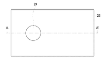
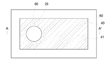
図11Aは本開示内容の第7実施例の発光素子の平面図である。図11Bは本開示内容の発光素子の図11AのA-A’線に沿う断面図である。本明細書では、特段の説明がない限り、同一の符号は、異なる図面において、本開示内容の全ての説明された同一又は略同一の構造、材料、材料組成及び/又は製造方法に対応する。本実施例では、基板10、第1DBRスタック21、発光スタック22及び第2DBRスタック23は第2実施例と略同一である。相違点として、コンタクト層24は第3幅W3を有し、第2DBRスタック23は第3幅W3よりも大きい第4幅W4を有する。発光素子は、コンタクト層24を覆い、且つ第1電極40とコンタクト層24との間に設けられた導電層60をさらに含む。導電層60は、第2DBRスタック23の第4幅W4に略等しい第5幅W5を有する。第1電極40は、導電層60の表面積の50%以上を覆う。好ましくは、第1電極40は導電層60の表面積の80%以上、より好ましくは、導電層60の表面積の90%以上を覆う。第1電極40の輪郭は導電層60の輪郭と略同一である。第1電極40は、コンタクト層24と直接接触することではなく、導電層60と直接接触する。放射放出領域Iは、コンタクト層24の直下に位置する第2DBRスタック23、発光スタック22及び第1DBRスタック21を含む。放射Rは第2開口25を介して発光素子から逃げる。
FIG. 11A is a plan view of the light emitting device according to the seventh embodiment of the present disclosure. FIG. 11B is a cross-sectional view taken along the line AA'of FIG. 11A of the light emitting element of the present disclosure. In the present specification, unless otherwise specified, the same reference numerals correspond to all described identical or substantially identical structures, materials, material compositions and / or manufacturing methods of the present disclosure in different drawings. In this embodiment, the
第2開口25は、コンタクト層24の直上に位置し、且つ下方の導電層60を露出させる。コンタクト層24の第3幅W3と第2開口25の第2最大幅W2との比は0.1~3であり、好ましくは、0.5~1.1であり、より好ましくは、0.6~0.8である。第3幅W3と第2最大幅W2との比を1よりも小さいものとすることで、第1電極40は放射放出領域Iにより放出された光を遮蔽しにくく、より多くの光は第2開口を介して逃げることができる。
The
第2DBRスタック23のコンタクト層24の直下に位置する部分の導電率は、第2DBRスタック23のコンタクト層24により覆われていない部分の導電率に略同一である。導電層60はnλ/4に近く、或いは等しい厚さを有し、λは発光スタック22から放出された放射のピーク波長であり、nは奇数の正整数である。導電層60は、透明の導電性金属酸化物の材料、例えばインジウムスズ酸化物(ITO)、アルミニウム亜鉛酸化物(AZO)、カドミウム錫酸化物(SnCdO)、アンチモンスズ酸化物(ATO)、亜鉛酸化物(ZnO)、亜鉛スズ酸化物(ZTO)、インジウム亜鉛酸化物(IZO)を含む。導電層60は、実質的に、発光スタック22により放出された放射を透過させることができる。
The conductivity of the portion directly below the
電流が第1電極40からエピタキシャル構造20に流入する際に、コンタクト層24と第2DBRスタック23との間の接触抵抗は、導電層60とエピタキシャル構造20との間の接触抵抗に比べて相対的に低いため、電流は殆ど導電層60からコンタクト層24に流れ、コンタクト層24を介してエピタキシャル構造20に流入する。即ち、第2DBRスタック23のコンタクト層24の直下に位置する部分の電流密度は、第2DBRスタック23のコンタクト層24により覆われていない部分の電流密度よりも高い。具体的には、エピタキシャル構造20の最上層、即ち本実施例のコンタクト層24は、エピタキシャル構造20のうち発光素子の制限後の電流を伝導する半導体層の1番目の層である。
When a current flows from the
図12Aは本開示内容の第7実施例の発光素子の光出力パワー(optical output power)と順方向電流(forward current)の関係曲線を示す図であり、ここで、コンタクト層24の第3幅W3と第2開口25の第2最大幅W2との比は約1である。図12Bは図12Aにおける領域Iの拡大図である。本実施例では、レーザ閾値電流Ithは約13ミリアンペアであり、飽和電流Isatは約79ミリアンペアである。レーザ閾値電流Ith、飽和電流Isat及びレーザ閾値電流Ithと飽和電流Isatの差は、異なる応用要求に応じてコンタクト層24の第3幅W3で調整されてもよい。例えば、高いレーザ閾値電流Ith、高い飽和電流Isat及び高いレーザ閾値電流Ithと飽和電流Isatの差が必要となる場合、第3幅W3が大きい方が好ましい。具体的には、レーザ閾値電流Ithと第3幅W3は次の式を満たす。
FIG. 12A is a diagram showing a relationship curve between the optical output power and the forward current of the light emitting element of the seventh embodiment of the present disclosure, wherein the third width of the
0.4W3(μm)-7≦Ith(ミリアンペア)≦0.4W3(μm)+7
1つの態様では、放射は約850±10ナノメートルのピーク波長を有する。1つの態様では、放射は約940±10ナノメートルのピーク波長を有する。
0.4W 3 (μm) -7 ≤ If (milliampere) ≤ 0.4W 3 (μm) +7
In one embodiment, the radiation has a peak wavelength of about 850 ± 10 nanometers. In one embodiment, the radiation has a peak wavelength of about 940 ± 10 nanometers.
表2は、異なる順方向電流の場合の第7実施例の発光素子の放射のファーフィールド角を示し、放射は約850±10ナノメートルのピーク波長を有する。 Table 2 shows the farfield angle of the emission of the light emitting element of the seventh embodiment for different forward currents, the emission having a peak wavelength of about 850 ± 10 nanometers.

表3は、異なる順方向電流の場合の第7実施例の発光素子の放射のファーフィールド角を示し、放射は約940±10ナノメートルのピーク波長を有する。本実施例では、レーザ閾値電流Ithは約13ミリアンペアであり、飽和電流Isatは約80ミリアンペアである。
Table 3 shows the farfield angle of the emission of the light emitting element of the seventh embodiment for different forward currents, the emission having a peak wavelength of about 940 ± 10 nanometers. In this embodiment, the laser threshold current Is is about 13mA and the saturation current Isat is about 80mA .

表2及び表3に示すように、順方向電流がレーザ閾値電流Ithよりも高く、且つ飽和電流Isatよりも低い場合、放射のファーフィールド角は15度よりも小さく、好ましくは、5度~15度であり、より好ましくは、8度~13度である。
As shown in Tables 2 and 3, when the forward current is higher than the laser threshold current I th and lower than the saturation current Isat, the farfield angle of radiation is less than 15 degrees, preferably 5 degrees. It is ~ 15 degrees, more preferably 8 degrees to 13 degrees.
本開示内容では、発光素子が第2DBRスタック23において酸化層及びイオン注入層を含む高抵抗構造を有しないが、コンタクト層24及び導電層60を含むことで、エピタキシャル構造20の最上層がエピタキシャル構造20の発光素子の制限後の電流を伝導する1番目の層となり、順方向電流がレーザ閾値電流Ithと飽和電流Isatとの間のものである場合、発光素子は15度よりも小さいファーフィールド角を有する。
In the present disclosure, the light emitting device does not have a high resistance structure including an oxide layer and an ion implantation layer in the
図13A乃至図16Bは図11A及び図11Bに示す発光素子の製造方法を示す図である。本方法は下記のステップを含む。 13A to 16B are diagrams showing a method of manufacturing the light emitting element shown in FIGS. 11A and 11B. The method includes the following steps.
a.図13A及び図13Bに示すように、基板10を提供する。
a. As shown in FIGS. 13A and 13B, the
b.エピタキシャル成長により基板10の上にエピタキシャル構造20を形成する。
b. The
c.フォトリソグラフィ・マスクによりコンタクト層24をパターン化する。
c. The
d.図14A及び図14Bに示すように、任意の適切な方法、例えばスパッタリング又は蒸着により、パターン化されたコンタクト層24を覆う導電層60を形成する。
d. As shown in FIGS. 14A and 14B, the
e.図15A及び図15Bに示すように、金属層60の上に金属層(図示せず)を形成する。
e. As shown in FIGS. 15A and 15B, a metal layer (not shown) is formed on the
f.フォトリソグラフィ・マスクにより金属層をパターン化し、第1電極40を形成して第1電極40内に第2開口25を形成する。ここで、第1電極40はコンタクト層24のパターンと略相補的なパターンを有し、即ち、コンタクト層24のパターンは第1電極40の第2開口25のパターンと略等しく、且つ第2開口25は概ねコンタクト層24の直上に位置する。
f. The metal layer is patterned by a photolithography mask to form the
g.図16A及び図16Bに示すように、エピタキシャル構造20の周辺部を除去して突出部26を形成する。突出部26は、露出している台部側壁261を含み、基板10の最も外側の縁部に比べて、第2開口25に近い。
g. As shown in FIGS. 16A and 16B, the peripheral portion of the
h.基板10のエピタキシャル構造20に対向する他方側に第2電極50を形成する。
h. The
i.ステップhにおいて形成された構造を切断し、図11A及び図11Bに示すそれぞれ形成された発光素子を取得する。 i. The structure formed in step h is cut to obtain the formed light emitting elements shown in FIGS. 11A and 11B, respectively.
本開示内容の方法は、第2DBRスタック23の一部の領域の導電率を低減させるステップ、例えば酸化領域の導電率、イオン注入領域の導電率又は図24に示すアンダーカットの導電率が第2DBRスタック23の処理領域以外の他部の導電率よりも低くするための、第2DBRスタック23のうち少なくとも1つの層を酸化する酸化ステップ、第2DBRスタック23のうち少なくとも1つの層において少なくとも導電率を低減させるイオンを注入するステップ、及び/又は第2DBRスタック23のうち少なくとも1つの層の周辺部を選択的にエッチングして図24に示すアンダーカットを形成するステップを含まない。酸化ステップ、イオン注入ステップ及び第2DBRスタック23のうち1つの層をエッチングするステップは、第2DBRスタック23の第1電極40の直下に位置する部分を略絶縁の領域に変換して第2DBRスタック23に高抵抗構造を形成するためのものである。好ましくは、本開示内容の方法は、パターン化プロセスにおいて、3種類以下の異なるフォトリソグラフィ・マスクを用いる。従って、本開示内容の発光素子の製造方法は簡単であり、且つ低コストの利点を有する。
In the method of the present disclosure, a step of reducing the conductivity of a part of the
図17Aは本開示内容の第8実施例の発光素子の平面図である。図17Bは本開示内容の発光素子の図17AのA-A’線に沿う断面図である。本明細書では、特段の説明がない限り、同一の符号は、異なる図面において、本開示内容の全ての説明された同一又は略同一の構造、材料、材料組成及び/又は製造方法に対応する。本開示内容の第8実施例の発光素子は、第7実施例と略同一の構成を含み、相違点として、発光素子は、エピタキシャル構造20、導電層60及び第1電極40と同一の形状を有するようにエピタキシャル構造20、導電層60及び第1電極40を覆うパッシベーション層110をさらに含む。パッシベーション層110は、リード線に接続するように、下方の第1電極40を露出させ、且つコンタクト層24から離れる開孔111を含む。図17A及び図17Bに示す発光素子の製造方法は図16A及び図16Bに示す発光素子の製造方法と略同一である。相違点として、露出する台部側壁261を含む突出部26を形成した後に、本方法は、エピタキシャル構造20の露出する台部側壁261、導電層60の側壁、第1電極40の側壁に沿って同一の形状を有するパッシベーション層110を形成するステップをさらに含み、パッシベーション層110は導電層60及び第1電極40を覆う。次に、パッシベーション層110をパターン化し、パッシベーション層110内に開孔111を形成して下方の第1電極40を露出させる。本開示内容の方法は、パターン化プロセスにおいて、4以下の異なるフォトリソグラフィ・マスクを用いる。従って、本開示内容の発光素子の製造方法は簡単であり、且つ低コストの利点を有する。
FIG. 17A is a plan view of the light emitting device according to the eighth embodiment of the present disclosure. FIG. 17B is a cross-sectional view taken along the line AA'of FIG. 17A of the light emitting element of the present disclosure. In the present specification, unless otherwise specified, the same reference numerals correspond to all described identical or substantially identical structures, materials, material compositions and / or manufacturing methods of the present disclosure in different drawings. The light emitting element of the eighth embodiment of the present disclosure includes substantially the same configuration as that of the seventh embodiment, and the difference is that the light emitting element has the same shape as the
図18は開示内容の第9実施例の発光素子の断面図であり、その平面図は図11Aと同じである。本明細書では、特段の説明がない限り、同一の符号は、異なる図面において、本開示内容の全ての説明された同一又は略同一の構造、材料、材料組成及び/又は製造方法に対応する。本開示内容の第9実施例の発光素子は、第7実施例と略同一の構成を含み、相違点として、本実施例の発光素子は、永久基板90、及び永久基板90とエピタキシャル構造20との間の接着層100を含む。本実施例では、永久基板90は、基板10の熱伝導率よりも高い熱伝導率を有する。接着層100は、永久基板90とエピタキシャル構造20とを接続させるために用いられる。図19A~図19Dは図18に示す発光素子の製造方法を示す図である。図18に示す発光素子の製造方法は図11A及び図11Bに示す発光素子の製造方法と略同一である。相違点として、コンタクト層24をパターン化する前に、図19Aに示すように、本方法は、一時的な接着層80によりエピタキシャル構造20を一時的な基板70に接着するステップをさらに含み、本実施例では、一時的な基板はガラスを含む。図19Bに示すように、任意の適切な方法により基板10を除去する。図19Cに示すように、接着層100によりエピタキシャル構造20を永久基板90に接着する。図19Dに示すように、一時的な基板70及び一時的な接着層80を除去する。本実施例では、接着ステップにより、発光素子は高い熱伝導率を有する永久基板90を含む。従って、発光素子は高い出力電力を達成できる。
FIG. 18 is a cross-sectional view of the light emitting element of the ninth embodiment of the disclosed contents, and the plan view thereof is the same as that of FIG. 11A. In the present specification, unless otherwise specified, the same reference numerals correspond to all described identical or substantially identical structures, materials, material compositions and / or manufacturing methods of the present disclosure in different drawings. The light emitting device of the ninth embodiment of the present disclosure includes substantially the same configuration as that of the seventh embodiment, and the difference is that the light emitting element of the present embodiment includes the
図20Aは本開示内容の第10実施例の発光素子の平面図である。図20Bは本開示内容の発光素子の図20AのA-A’線に沿う断面図である。本明細書では、特段の説明がない限り、同一の符号は、異なる図面において、本開示内容の全ての説明された同一又は略同一の構造、材料、材料組成及び/又は製造方法に対応する。本開示内容の第10実施例の発光素子は、第7実施例と略同一の構成を含み、相違点として、本実施例の発光素子は、単一ダイにおいて、アレイ状に配列された複数の放射放出領域Iを含む。具体的には、コンタクト層24は複数の分離しているコンタクト領域241を含み、図20Aに示すように、コンタクト領域241は二次元のアレイ状に配列されている。各コンタクト領域241は第3幅W3を有する。本実施例では、複数のコンタクト領域241の第3幅W3は略等しい。図20Bに示すように、導電層60は、連続的な層であり、且つ複数の分離しているコンタクト領域241を覆う。第1電極40は導電層60上に位置し、且つ連続的な層である。複数の第2開口25は第1電極40内に形成され、且つ互いに分離し、各第2開口25は対応するコンタクト領域241に位置合わせるように形成される。第2開口25は導電層60を露出させる。コンタクト領域241の第3幅W3と対応する第2開口25の第2幅W2との比は0.1~3であり、好ましくは、0.9~1.1である。本実施例では、各比は略同一である。コンタクト層24の直下に位置する第2DBRスタック23、発光スタック22及び第1DBRスタック21は放射放出領域Iとなる。コンタクト領域241及び第2開口25の数は本実施例に限定されず、放射放出領域Iの配置方法も本実施例に限定されない。例えば放射放出領域Iは交差するように配列されてもよいし、隣接する2つの行及び/又は列の放射放出領域Iの数は異なってもよい。具体的には、エピタキシャル構造20の最上層、即ち本実施例のコンタクト層24は、エピタキシャル構造20のうち発光素子の制限後の電流を伝導する半導体層の1番目の層である。
FIG. 20A is a plan view of the light emitting device according to the tenth embodiment of the present disclosure. FIG. 20B is a cross-sectional view of the light emitting device of the present disclosure content along the line AA'of FIG. 20A. In the present specification, unless otherwise specified, the same reference numerals correspond to all described identical or substantially identical structures, materials, material compositions and / or manufacturing methods of the present disclosure in different drawings. The light emitting elements of the tenth embodiment of the present disclosure include substantially the same configuration as that of the seventh embodiment, and the difference is that the light emitting elements of the present embodiment have a plurality of light emitting elements arranged in an array on a single die. Includes radiation emission region I. Specifically, the
図21Aは本開示内容の第11実施例の発光素子の平面図である。図21Bは本開示内容の発光素子の図21AのA-A’線に沿う断面図である。本明細書では、特段の説明がない限り、同一の符号は、異なる図面において、本開示内容の全ての説明された同一又は略同一の構造、材料、材料組成及び/又は製造方法に対応する。本開示内容の第11実施例の発光素子は、第10実施例と略同一の構成を含み、相違点として、本実施例の発光素子は、少なくとも1つのコンタクト領域241の第3幅W3’は他のコンタクト領域241の第3幅W3と異なり、複数の異なるレーザ閾値電流Ithを有する。本実施例では、図21Bに示すように、中央のコンタクト領域241の第3幅W3’は他のコンタクト領域241の第3幅W3よりも小さい。中央のコンタクト領域241の第3幅W3’と他の2つのコンタクト領域241のうち1つの第3幅W3との差は3ミクロン(μm)以上であり、好ましくは、8ミクロンよりも大きく、且つ40ミクロンよりも小さい。図21に示すように、中央のコンタクト領域241に対応する第2開口25は他の第2開口25よりも小さい。コンタクト領域241の第3幅と各コンタクト領域241に対応する第2開口25の第2最大幅W2との比は0.1~3であり、好ましくは、0.5~1.1であり、より好ましくは、0.6~0.8である。発光素子は複数の異なるレーザ閾値電流Ithを有する。各レーザ閾値電流Ithは、放射放出領域Iにコヒーレント光を発生させるために用いられる。具体的には、中央のコンタクト領域241の第3幅W3’が他のコンタクト領域241の第3幅W3よりも小さいため、中央の放射放出領域Iにコヒーレント光を放出させるためのレーザ閾値電流Ithは他の2つの放射放出領域Iのうち1つにコヒーレント光を放出させるためのレーザ閾値電流Ithよりも小さい。このため、本実施例では、順方向電流が中央の放射放出領域Iにコヒーレント光を放出させるためのレーザ閾値電流Ithよりも大きく、且つ他の放射放出領域Iにコヒーレント光を放出させるためのレーザ閾値電流Ithよりも小さい場合、中央の放射放出領域Iにより放出された放射は15度よりも小さいファーフィールド角を有するコヒーレント光であるが、他の放射放出領域Iにより放出された放射は60度よりも大きいファーフィールド角を有する非コヒーレント光である。従って、発光素子は、遠距離及び近距離の両方の特性が必要な応用、例えば監視機器に適用する。第3幅を有するコンタクト領域241の配置方法は本実施例に限定されない。例えば、他のコンタクト領域241の第3幅よりも小さい第3幅を有するコンタクト領域241を端部に設けてもよい。或いは、交差して配列するように、比較的に小さい第3幅を有するコンタクト領域241及び比較的に大きい第3幅を有するコンタクト領域241を行及び/又は列ごとに間隔を空けて設けてもよい。
FIG. 21A is a plan view of the light emitting device according to the eleventh embodiment of the present disclosure. FIG. 21B is a cross-sectional view of the light emitting device of the present disclosure content along the line AA'of FIG. 21A. In the present specification, unless otherwise specified, the same reference numerals correspond to all described identical or substantially identical structures, materials, material compositions and / or manufacturing methods of the present disclosure in different drawings. The light emitting element of the eleventh embodiment of the present disclosure includes substantially the same configuration as that of the tenth embodiment, and the difference is that the light emitting element of the present embodiment has a third width W 3'of at least one
図22は本開示内容の第12実施例の発光素子の平面図である。本明細書では、特段の説明がない限り、同一の符号は、異なる図面において、本開示内容の全ての説明された同一又は略同一の構造、材料、材料組成及び/又は製造方法に対応する。本開示内容の第12実施例の発光素子は、第11実施例と略同一の構成を含み、相違点として、本実施例の発光素子は、複数の互いに同一のレーザ閾値電流Ithを有する。各レーザ閾値電流Ithは、放射放出領域Iにコヒーレント光を発生させるために用いられる。第1電極40の異なるレイアウトに応じて、異なる量の電流が異なるコンタクト領域241に流入するように制御し、電流が発光素子に流入する際に、他のコンタクト領域241により吸引された電流に比べて、1つのコンタクト領域241はより多い電流を吸引する。具体的には、本実施例では、中央のコンタクト領域241の幅は他のコンタクト領域241の幅に略等しい。中央のコンタクト領域241に対応する第2開口25の幅は他の第2開口25の幅に略等しい。図21Aに示す第1電極40に比べると、本実施例の導電層60上の第1電極40は異なるレイアウトを有する。具体的には、第1電極は、ワイヤボンディング部、複数の第1延在電極44及び第2延在電極45を含む。ワイヤボンディング部41はリード線に接続するために用いられる。各第1延在電極44は第2開口25を囲む。各第2延在電極45は、実質的にワイヤボンディング部41から垂直に延伸し、且つ少なくとも3つの第1延在電極44に接続する。本実施例では、各第1延在電極44の幅は略同一である。各第2延在電極45の幅は略同一である。中央の第2開口25を囲む第1延在電極44は2つの第2延在電極45に接続し、他の2つの第2開口25を囲む第1延在電極44は1つのみの第2延在電極45に接続する。このため、発光素子を駆動する際に、他のコンタクト領域241により吸引された電流に比べて、中央のコンタクト領域241はより多い電流を吸引する。中央の各コンタクト領域241を流れる順方向電流が対応する放射放出領域Iのレーザ閾値電流Ithに達した場合、他の2つの各コンタクト領域241を流れる順方向電流は、依然として対応する放射放出領域Iのレーザ閾値電流Ithよりも低い。このため、中央の放射放出領域Iにより放出された放射は15度よりも小さいファーフィールド角を有するコヒーレント光であるが、他の放射放出領域Iにより放出された放射は60度よりも大きいファーフィールド角を有する非コヒーレント光である。従って、発光素子は、遠距離及び近距離の両方の特性が必要な応用、例えば監視機器に適用する。もう1つの態様では、類似の結果を達成するために、中央の第1延在電極44の幅は他の2つの第1延在電極44の幅よりも大きくてもよい。もう1つの態様では、類似の結果を達成するために、中央の第2延在電極45の幅は他の2つの第2延在電極45の幅よりも大きく、且つ2つの第2延在電極45が中央の第1延在電極44に接続することを含まなくてもよい。第1延在電極44及び第2延在電極45の配置方法は本実施例に限定されない。例えば、端部の第2開口25を囲む第1延在電極44は2つの第2延在電極45に接続してもよく、第1延在電極44の幅及び第2延在電極45の幅をそれに応じて変更してもよい。
FIG. 22 is a plan view of the light emitting device according to the twelfth embodiment of the present disclosure. In the present specification, unless otherwise specified, the same reference numerals correspond to all described identical or substantially identical structures, materials, material compositions and / or manufacturing methods of the present disclosure in different drawings. The light emitting element of the twelfth embodiment of the present disclosure includes substantially the same configuration as that of the eleventh embodiment, and the difference is that the light emitting element of the present embodiment has a plurality of laser threshold currents that are the same as each other. Each laser threshold current I th is used to generate coherent light in the radiation emission region I. Depending on the different layout of the
図23は本開示内容の第13実施例の発光素子の平面図である。特段の説明がない限り、同一の符号は、異なる図面において、本開示内容の全ての説明された同一又は略同一の構造、材料、材料組成及び/又は製造方法に対応する。本開示内容の第13実施例の発光素子は、第12実施例と略同一の構成を含み、相違点として、本実施例の発光素子の導電層60上に位置する第1電極40は異なるパターンを有する。第1電極40は幅を有する第3延在電極46を含み、第3延在電極46の幅は第1延在電極44の幅及び第2延在電極45の幅よりも大きい。このため、第2開口25の周辺の第1延在電極44及び第2延在電極45により覆われている領域に比べて、第3延在電極46は第2開口25の周辺のより広い領域を覆う。よって、中央の第2開口25を囲む導電層60と第1電極40との間の接触面積は、他の第2開口25を囲む導電層60と第1電極40との間の接触面積よりも大きい。このため、発光素子を駆動する際に、他のコンタクト領域241により吸引された電流に比べて、中央のコンタクト領域241はより多い電流を吸引する。中央の各コンタクト領域241を流れる順方向電流が対応する放射放出領域Iのレーザ閾値電流Ithに達した場合、他の2つの各コンタクト領域241を流れる順方向電流は、依然として対応する放射放出領域Iのレーザ閾値電流Ithよりも低い。このため、中央の放射放出領域Iにより放出された放射は15度よりも小さいファーフィールド角を有するコヒーレント光であるが、他の放射放出領域Iにより放出された放射は60度よりも大きいファーフィールド角を有する非コヒーレント光である。従って、発光素子は、遠距離及び近距離の両方の特性が必要な応用、例えば監視機器に適用する。第1延在電極44及び第2延在電極45のパターンは本実施例に限定されない。例えば、第1電極40は、中央の第2開口25でなく、端部の第2開口25のより多い周辺領域を覆ってもよい。
FIG. 23 is a plan view of the light emitting device according to the thirteenth embodiment of the present disclosure. Unless otherwise specified, the same reference numerals correspond to all described identical or substantially identical structures, materials, material compositions and / or manufacturing methods of the present disclosure in different drawings. The light emitting element of the thirteenth embodiment of the present disclosure includes substantially the same configuration as that of the twelfth embodiment, and the difference is that the
発光スタック22は活性領域を含み、活性領域は単一ヘテロ構造(SH:single heterostructure)、ダブルヘテロ構造(DH:double heterostructure)又は多重量子井戸(MQW)を含む。好ましくは、活性領域は多重量子井戸(MQW)を含み、多重量子井戸は交互に設けられた井戸層とバリア層を含む。各バリア層のエネルギーレベルは井戸層のエネルギーレベルよりも大きい。活性領域により放出されたピーク波長は井戸層の厚さ又は材料を変更することで変更される。好ましくは、井戸層の材料はIII-V族半導体材料、例えばひ化ガリウムアルミニウム(AlGaAs)を含む。バリア層の材料は、III-V族半導体材料、例えばひ化ガリウムアルミニウム(AlGaAs)を含む。発光スタック22は、発光スタック22の厚さを調整してnλ/2の厚さに近く、或いは等しくするように、活性領域と第1DBRスタック21との間及び/又は活性領域と第2DBRスタック23との間にスペーサ層をさらに含んでもよく、ここで、λは発光スタック22により放出された放射のピーク波長であり、nは正整数である。スペーサ層の材料はIII-V族半導体材料、例えばひ化ガリウムアルミニウム(AlGaAs)を含む。
The
第1DBRスタック21及び第2DBRスタック23は複数の交互に設けられた高屈折率半導体層及び低屈折率半導体層を含む。第1DBRスタック21及び第2DBRスタック23の材料は、III-V族半導体材料、例えばひ化ガリウムアルミニウムAlxGa(1-x)As/AlyGa(1-y)Asを含み、xはyに等しくなく、アルミニウム及びガリウムの含有量を調整して波長範囲の光を反射してもよい。各半導体層はλ/4nに近く、或いは等しい厚さを有し、λは発光スタック22により放出された放射のピーク波長であり、nは層の屈折率である。第1DBRスタック21はピーク波長において99%以上の反射率を有する。第2DBRスタック23はピーク波長において98%以上の反射率を有する。好ましくは、第1DBRスタック21の反射率は第2DBRスタック23の反射率よりも大きい。第1DBRスタック21の組の数は第2DBRスタック23の組の数よりも大きく、高屈折率半導体層及び低屈折率半導体層を1つの組と見なされる。好ましくは、第1DBRスタック21の組の数は15よりも大きく、より好ましくは、30よりも大きく、且つ80よりも小さい。第2DBRスタック23の組の数は15よりも大きく、より好ましくは、20よりも大きく、且つ80よりも小さい。
The
本実施例では、基板10は、エピタキシャル構造20をエピタキシャル成長するための上面を有する。基板10は、基板10上に成長された層又は構造を十分に支持できる厚さを有する。好ましくは、基板10の厚さは、100ミクロン以上であり、より好ましくは、250ミクロン以下である。基板10は、単結晶基板であり、半導体材料、例えばIII-V族半導体材料又はIV族半導体材料を含む。1つの態様では、基板は、n型又はp型のIII-V族半導体材料を含む。本実施例では、III-V族半導体材料は、n型のヒ化ガリウム(GaAs)、n型ドーパントはケイ素(Si)である。
In this embodiment, the
永久基板80は、導電的なものであり、第1電極40と第2電極50との間で電流を伝導する。永久基板80は、その上の層又は構造を十分に支持できる厚さ、例えば100ミクロン以上の厚さを有する。永久基板80は、ケイ素(Si)、ゲルマニウム(Ge)、銅(Cu)、モリブデン(Mo)、タングステン-モリブデン(MoW)、窒化アルミニウム(AlN)、酸化亜鉛(ZnO)又は銅-タングステン(CuW)を含む導電材料を含む。好ましくは、永久基板80は、ケイ素又は銅-タングステン(CuW)を含む。
The permanent substrate 80 is conductive and conducts a current between the
第1電極40及び第2電極50は外部電源に接続し、且つ両者の間に電流を伝導するために用いられる。第1電極40及び第2電極50の材料は、透明導電材料又は金属材料を含む。透明導電材料は透明の導電酸化物を含み、金属材料は、金(Au)、白金(Pt)、ゲルマニウム-ニッケル-金(GeAuNi)、チタン(Ti)、ベリリウム-金(BeAu)、ゲルマニウム-金(GeAu)、アルミニウム(Al)、亜鉛-金(ZnAu)又はニッケルを含む。
The
第1電極40はコンタクト層24及び第2DBRスタック23により低抵抗接触又はオーム接触を形成し、第1電極40と第2DBRスタック23との間の抵抗は10-2ohm-cmよりも低い。コンタクト層24の導電形態は第2DBRスタック23の導電形態と同じである。1つの態様では、コンタクト層24はp型であり、且つ高いp型ドープ濃度を有し、例えば、1018/cm3よりも高く、好ましくは、1019/cm3よりも高く、より好ましくは、1×1019/cm3~5×1022/cm3である(両者を共に含む)。コンタクト層24の材料は、III-V族半導体材料、例えばひ化ガリウム(GaAs)又はひ化ガリウムアルミニウム(AlGaAs)を含む。
The
接着層100及び/又は一時的な接着層80は、透明導電酸化物、金属材料、絶縁酸化物又はポリマー材料を含む。透明導電酸化物は、酸化インジウムスズ(ITO)、酸化インジウム(InO)、酸化スズ(SnO)、酸化カドミウム錫(CTO)、酸化アンチモンスズ(ATO)、酸化アルミニウム亜鉛(AZO)、酸化亜鉛スズ(ZTO)、酸化ガリウム亜鉛(GZO)、酸化インジウムタングステン(IWO)、酸化亜鉛(ZnO)、酸化インジウム亜鉛(IZO)を含む。金属材料は、インジウム、スズ、金、チタン、ニッケル、白金、タングステン又はそれらの合金を含む。絶縁酸化物は、アルミナ(AlOx)、酸化ケイ素(SiOx)又は窒酸化ケイ素(SiOxNy)を含む。ポリマー材料は、エポキシ樹脂(epoxy)、ポリイミド(polyimide)、ペルフルオロシクロブタン(perfluorocyclobutane)、ベンゾシクロブテン(BCB:benzocyclobutene)又はシリコーン(silicone)を含む。接着層100は、400ナノメートル~5000ナノメートルの厚さを有する。
The
エピタキシャルの方法は、有機金属化学気相成長法(MOCVD:metal-organic chemical vapor deposition)、ハイドライド気相成長法(HVPE:hydride vapor phase epitaxy)、分子線エピタキシー法(MBE:molecular beam epitaxy)、液相エピタキシー法(LPE:liquid-phase epitaxy)を含むが、これらに限定されない。 The epitaxial method is organic metal chemical vapor deposition (MOCVD), hydride vapor deposition (HVPE), molecular beam epitaxy (MBE) epitaxy, molecular beam epitaxy (MBE) It includes, but is not limited to, the phase epitaxy method (LPE: liquid-phase epitaxy).
本開示内容の他の実施例では、上記実施例の構造を組み合わせ、或いは変更してもよい。例えば、図1A又は図1bに示す発光素子はパッシベーション層を含んでもよい。 In other embodiments of the present disclosure, the structures of the above embodiments may be combined or modified. For example, the light emitting element shown in FIG. 1A or FIG. 1b may include a passivation layer.
なお、本発明の列記した各実施例は単なる本発明を説明するためのものであり、本発明の範囲を限定するものではない。本発明の主旨又は範囲から逸脱することなく、本発明について明らかな修正又は変更を行ってもよい。異なる実施例における同一若しくは類似の構成要件、又は異なる実施例における同一の符号を有する構成要件は同一の物理的若しくは化学的な特性を有する。また、本発明の実施例は、適切な場合に、互いに組合せ又は置換してもよく、上述した特定の実施例に限定されない。1つの実施例において詳細に説明された特定の構成要件と他の構成要件との接続関係は他の実施例にも適用されてもよく、本発明の権利保護の範囲に属するものである。 It should be noted that the examples listed in the present invention are merely for explaining the present invention, and do not limit the scope of the present invention. You may make obvious modifications or changes to the invention without departing from the gist or scope of the invention. The same or similar constituents in different embodiments, or constituents with the same reference numerals in different embodiments, have the same physical or chemical properties. Moreover, the examples of the present invention may be combined or substituted with each other, if appropriate, and are not limited to the specific examples described above. The connection relationship between a specific configuration requirement and another configuration requirement described in detail in one embodiment may be applied to other embodiments and belongs to the scope of protection of rights of the present invention.
10 基板
20 エピタキシャル構造
30 電流ブロック層
40 第1電極
50 第2電極
60 導電層
21 第1DBRスタック
31 第1開口
22 発光スタック
23 第2DBRスタック
24 コンタクト層
25 第2開口
W1 第1最大幅
W2 第2最大幅
R 放射
41 ワイヤボンディング部
42 電流注入部
43 ブリッジング部
I 放射放出領域
26 突出部
261 台部側壁
301 内部
302 外部
W3 第3幅
W4 第4幅
W5 第5幅
W3’ 第3幅
Ith レーザ閾値電流
110 パッシベーション層
111 開孔
90 永久基板
100 接着層
70 一時的な基板
44 第1延在電極
45 第2延在電極
46 第3延在電極
241 コンタクト領域
Isat 飽和電流Isat
10
Claims (10)
基板と、
前記基板の上に位置し、且つ第1部分及び第2部分を含むエピタキシャル構造であって、前記第1部分及び前記第2部分のそれぞれは、第1DBRスタック、発光スタック、第2DBRスタック及びコンタクト層を順次含む、エピタキシャル構造と、
前記エピタキシャル構造の上に位置する電極と、
前記コンタクト層と前記電極との間に位置する電流ブロック層と、
前記電流ブロック層の中に形成された複数の第1開口であって、前記複数の第1開口のうちの2つの第1開口は、前記第1部分及び前記第2部分にそれぞれ対応する、複数の第1開口と、を含み、
前記電極は、前記複数の第1開口の中に埋め込まれ、且つ前記コンタクト層と接触し、
前記第1部分の前記第2DBRスタックは、前記第2部分の前記第2DBRスタックに接続する、発光素子。 It is a light emitting element
With the board
An epitaxial structure that is located on the substrate and includes a first portion and a second portion, each of the first portion and the second portion is a first DBR stack, a light emitting stack, a second DBR stack, and a contact layer. Including epitaxial structures and
An electrode located on the epitaxial structure and
A current block layer located between the contact layer and the electrode,
A plurality of first openings formed in the current block layer, wherein the two first openings of the plurality of first openings correspond to the first portion and the second portion, respectively. Including the first opening of
The electrode is embedded in the plurality of first openings and is in contact with the contact layer.
The second DBR stack of the first portion is a light emitting element connected to the second DBR stack of the second portion.
前記第1部分は、前記第2部分よりも前記発光面の中央に近く、
前記第1電流は、前記第2電流よりも大きい、請求項9に記載の発光素子。 The light emitting element has a light emitting surface and has a light emitting surface.
The first portion is closer to the center of the light emitting surface than the second portion .
The light emitting element according to claim 9 , wherein the first current is larger than the second current .
Priority Applications (1)
| Application Number | Priority Date | Filing Date | Title |
|---|---|---|---|
| JP2022075846A JP2022093631A (en) | 2016-03-07 | 2022-05-02 | Light-emitting element |
Applications Claiming Priority (2)
| Application Number | Priority Date | Filing Date | Title |
|---|---|---|---|
| US15/062,995 US9837792B2 (en) | 2016-03-07 | 2016-03-07 | Light-emitting device |
| US15/062,995 | 2016-03-07 |
Related Child Applications (1)
| Application Number | Title | Priority Date | Filing Date |
|---|---|---|---|
| JP2022075846A Division JP2022093631A (en) | 2016-03-07 | 2022-05-02 | Light-emitting element |
Publications (3)
| Publication Number | Publication Date |
|---|---|
| JP2017163140A JP2017163140A (en) | 2017-09-14 |
| JP2017163140A5 JP2017163140A5 (en) | 2020-04-09 |
| JP7068772B2 true JP7068772B2 (en) | 2022-05-17 |
Family
ID=59650704
Family Applications (2)
| Application Number | Title | Priority Date | Filing Date |
|---|---|---|---|
| JP2017038861A Active JP7068772B2 (en) | 2016-03-07 | 2017-03-02 | Light emitting element |
| JP2022075846A Pending JP2022093631A (en) | 2016-03-07 | 2022-05-02 | Light-emitting element |
Family Applications After (1)
| Application Number | Title | Priority Date | Filing Date |
|---|---|---|---|
| JP2022075846A Pending JP2022093631A (en) | 2016-03-07 | 2022-05-02 | Light-emitting element |
Country Status (6)
| Country | Link |
|---|---|
| US (3) | US9837792B2 (en) |
| JP (2) | JP7068772B2 (en) |
| KR (1) | KR102336974B1 (en) |
| CN (1) | CN107171180A (en) |
| DE (1) | DE102017101731A1 (en) |
| TW (3) | TW202322503A (en) |
Families Citing this family (9)
| Publication number | Priority date | Publication date | Assignee | Title |
|---|---|---|---|---|
| US11381060B2 (en) | 2017-04-04 | 2022-07-05 | Apple Inc. | VCSELs with improved optical and electrical confinement |
| WO2019181757A1 (en) * | 2018-03-19 | 2019-09-26 | Ricoh Company, Ltd. | Surface-emitting laser array, detection device, and laser device |
| WO2020205166A1 (en) * | 2019-04-01 | 2020-10-08 | Apple Inc. | Vcsel array with tight pitch and high efficiency |
| US20200365767A1 (en) * | 2019-05-17 | 2020-11-19 | Shin-Etsu Opto Electronic Co., Ltd. | Light-emitting diode structure and method for forming the same |
| US11374381B1 (en) | 2019-06-10 | 2022-06-28 | Apple Inc. | Integrated laser module |
| JP7056628B2 (en) * | 2019-06-28 | 2022-04-19 | セイコーエプソン株式会社 | Luminous device and projector |
| CN113410349B (en) * | 2021-04-30 | 2022-05-13 | 华灿光电(苏州)有限公司 | Light-emitting diode chip with double-layer Bragg reflector and preparation method thereof |
| CN113488568B (en) * | 2021-05-12 | 2022-06-14 | 华灿光电(浙江)有限公司 | Flip light-emitting diode chip and preparation method thereof |
| CN116565093A (en) * | 2023-07-11 | 2023-08-08 | 江西兆驰半导体有限公司 | LED chip preparation method and LED chip |
Citations (3)
| Publication number | Priority date | Publication date | Assignee | Title |
|---|---|---|---|---|
| JP2000031589A (en) | 1998-07-08 | 2000-01-28 | Oki Electric Ind Co Ltd | Semiconductor light emitting device |
| JP2000277852A (en) | 1999-03-24 | 2000-10-06 | Fuji Xerox Co Ltd | Surface emitting semiconductor laser and manufacturing method |
| JP2013171892A (en) | 2012-02-20 | 2013-09-02 | Ricoh Co Ltd | Optical sensor and image forming device |
Family Cites Families (31)
| Publication number | Priority date | Publication date | Assignee | Title |
|---|---|---|---|---|
| US3835415A (en) * | 1972-06-28 | 1974-09-10 | Ibm | High radiance semiconductor laser |
| US5008889A (en) * | 1989-11-06 | 1991-04-16 | Wilson Keith E | High-accuracy wavelength stabilization of angled-stripe super luminescent laser diode sources |
| JP3635880B2 (en) * | 1997-07-25 | 2005-04-06 | セイコーエプソン株式会社 | Surface emitting semiconductor laser and manufacturing method thereof |
| JP3551718B2 (en) * | 1997-08-18 | 2004-08-11 | 富士ゼロックス株式会社 | Surface emitting semiconductor laser |
| JP2000299492A (en) | 1999-04-15 | 2000-10-24 | Daido Steel Co Ltd | Quantum well type light emitting diode |
| JP3837969B2 (en) * | 1999-07-06 | 2006-10-25 | 富士ゼロックス株式会社 | Surface emitting semiconductor laser and manufacturing method thereof |
| JP2002289976A (en) * | 2001-03-23 | 2002-10-04 | Ricoh Co Ltd | Semiconductor structure, its manufacturing method and semiconductor laser element, semiconductor laser array as well as optical interconnection system and optical lan system |
| KR100909733B1 (en) * | 2002-01-28 | 2009-07-29 | 니치아 카가쿠 고교 가부시키가이샤 | Nitride semiconductor device having support substrate and manufacturing method thereof |
| JP4366522B2 (en) * | 2002-11-29 | 2009-11-18 | 信越半導体株式会社 | Light emitting element |
| JP2004193330A (en) * | 2002-12-11 | 2004-07-08 | Sharp Corp | Monolithic multiwavelength laser element and its manufacturing method |
| JP2004288674A (en) * | 2003-03-19 | 2004-10-14 | Fuji Xerox Co Ltd | Surface-emitting semiconductor laser and optical communication system using it |
| TW200505120A (en) * | 2003-07-29 | 2005-02-01 | Copax Photonics Corp | Single transverse mode vertical cavity surface emitting laser device with array structure and method for fabricating the same |
| KR20050019485A (en) * | 2003-08-19 | 2005-03-03 | 삼성전자주식회사 | Vertical cavity Surface Emitting Laser with integrated photodetector |
| JP4138629B2 (en) * | 2003-11-06 | 2008-08-27 | 株式会社東芝 | Surface emitting semiconductor device and manufacturing method thereof |
| DE102004004781A1 (en) * | 2004-01-30 | 2005-08-18 | Osram Opto Semiconductors Gmbh | Radiation-emitting semiconductor component has first active zone for generating coherent radiation of first wavelength and second active zone for generating incoherent radiation of second wavelength |
| US7889774B2 (en) * | 2004-03-05 | 2011-02-15 | The Trustees Of Princeton University | Organic polariton laser |
| JP4899344B2 (en) | 2004-06-29 | 2012-03-21 | 富士ゼロックス株式会社 | Surface emitting semiconductor laser and manufacturing method thereof |
| EP1703603B1 (en) * | 2005-03-17 | 2015-03-18 | Fujitsu Limited | Tunable laser |
| JP2007294732A (en) * | 2006-04-26 | 2007-11-08 | Matsushita Electric Ind Co Ltd | Semiconductor laser device and method of manufacturing the same |
| JP2008028120A (en) * | 2006-07-20 | 2008-02-07 | Sumitomo Electric Ind Ltd | Surface-emitting semiconductor element |
| JP4878322B2 (en) * | 2007-03-29 | 2012-02-15 | 古河電気工業株式会社 | Surface emitting laser element and method for manufacturing surface emitting laser element |
| DE102008012859B4 (en) * | 2007-12-21 | 2023-10-05 | OSRAM Opto Semiconductors Gesellschaft mit beschränkter Haftung | Laser light source with a filter structure |
| JP2009246291A (en) * | 2008-03-31 | 2009-10-22 | Furukawa Electric Co Ltd:The | Surface emitting laser element array |
| KR101438818B1 (en) * | 2008-04-01 | 2014-09-05 | 엘지이노텍 주식회사 | light emitting diode |
| JP2010219287A (en) * | 2009-03-17 | 2010-09-30 | Sony Corp | Semiconductor light emitting element and method for manufacturing thereof |
| JP5475398B2 (en) * | 2009-05-15 | 2014-04-16 | 日本オクラロ株式会社 | Semiconductor light emitting device |
| JP2011165869A (en) * | 2010-02-09 | 2011-08-25 | Mitsubishi Electric Corp | Semiconductor light-emitting element and method for manufacturing the same |
| KR20120131983A (en) * | 2011-05-27 | 2012-12-05 | 삼성전자주식회사 | Semiconductor light emitting device having current blocking layer |
| JP6303255B2 (en) * | 2011-12-02 | 2018-04-04 | 株式会社リコー | Surface emitting laser element and atomic oscillator |
| JP2015103727A (en) * | 2013-11-27 | 2015-06-04 | 株式会社村田製作所 | Manufacturing method for vertical resonator type surface light emission laser |
| US20150255954A1 (en) * | 2014-03-05 | 2015-09-10 | The Board Of Trustees Of The University Of Illinois | Method And Device For Producing Laser Emission |
-
2016
- 2016-03-07 US US15/062,995 patent/US9837792B2/en active Active
-
2017
- 2017-01-30 DE DE102017101731.3A patent/DE102017101731A1/en active Pending
- 2017-03-02 TW TW112103232A patent/TW202322503A/en unknown
- 2017-03-02 TW TW106106890A patent/TWI734750B/en active
- 2017-03-02 TW TW110123117A patent/TWI794849B/en active
- 2017-03-02 JP JP2017038861A patent/JP7068772B2/en active Active
- 2017-03-07 KR KR1020170028823A patent/KR102336974B1/en active IP Right Grant
- 2017-03-07 CN CN201710130811.7A patent/CN107171180A/en active Pending
- 2017-10-26 US US15/794,756 patent/US10090643B2/en active Active
-
2018
- 2018-08-21 US US16/106,458 patent/US10511140B2/en active Active
-
2022
- 2022-05-02 JP JP2022075846A patent/JP2022093631A/en active Pending
Patent Citations (3)
| Publication number | Priority date | Publication date | Assignee | Title |
|---|---|---|---|---|
| JP2000031589A (en) | 1998-07-08 | 2000-01-28 | Oki Electric Ind Co Ltd | Semiconductor light emitting device |
| JP2000277852A (en) | 1999-03-24 | 2000-10-06 | Fuji Xerox Co Ltd | Surface emitting semiconductor laser and manufacturing method |
| JP2013171892A (en) | 2012-02-20 | 2013-09-02 | Ricoh Co Ltd | Optical sensor and image forming device |
Also Published As
| Publication number | Publication date |
|---|---|
| US20180048119A1 (en) | 2018-02-15 |
| US10511140B2 (en) | 2019-12-17 |
| TW202322503A (en) | 2023-06-01 |
| TW201801431A (en) | 2018-01-01 |
| KR20170104401A (en) | 2017-09-15 |
| US20170256914A1 (en) | 2017-09-07 |
| TWI794849B (en) | 2023-03-01 |
| TW202139549A (en) | 2021-10-16 |
| US20180358780A1 (en) | 2018-12-13 |
| DE102017101731A1 (en) | 2017-09-07 |
| KR102336974B1 (en) | 2021-12-08 |
| JP2022093631A (en) | 2022-06-23 |
| US10090643B2 (en) | 2018-10-02 |
| US9837792B2 (en) | 2017-12-05 |
| CN107171180A (en) | 2017-09-15 |
| TWI734750B (en) | 2021-08-01 |
| JP2017163140A (en) | 2017-09-14 |
Similar Documents
| Publication | Publication Date | Title |
|---|---|---|
| JP7068772B2 (en) | Light emitting element | |
| US20230261148A1 (en) | Light-emitting device | |
| US9825088B2 (en) | Light-emitting device and manufacturing method thereof | |
| US7714343B2 (en) | Light emitting device | |
| US10756960B2 (en) | Light-emitting device | |
| JP2017050463A (en) | Surface emission semiconductor laser array and manufacturing method of surface emission semiconductor laser array | |
| US20230067254A1 (en) | Semiconductor device | |
| US20230135799A1 (en) | Light-emitting device | |
| US11894489B2 (en) | Semiconductor device, semiconductor component and display panel including the same | |
| US11588072B2 (en) | Semiconductor device and semiconductor component including ihe same | |
| JP2017147461A (en) | Surface-emitting semiconductor laser array | |
| US20230058195A1 (en) | Semiconductor device | |
| US20230129560A1 (en) | Semiconductor device and semiconductor component including the same | |
| TW202406173A (en) | Semiconductor device | |
| JP2020010056A (en) | Semiconductor light-emitting component |
Legal Events
| Date | Code | Title | Description |
|---|---|---|---|
| A521 | Request for written amendment filed |
Free format text: JAPANESE INTERMEDIATE CODE: A523 Effective date: 20200302 |
|
| A621 | Written request for application examination |
Free format text: JAPANESE INTERMEDIATE CODE: A621 Effective date: 20200302 |
|
| A977 | Report on retrieval |
Free format text: JAPANESE INTERMEDIATE CODE: A971007 Effective date: 20210322 |
|
| A131 | Notification of reasons for refusal |
Free format text: JAPANESE INTERMEDIATE CODE: A131 Effective date: 20210413 |
|
| A521 | Request for written amendment filed |
Free format text: JAPANESE INTERMEDIATE CODE: A523 Effective date: 20210708 |
|
| A131 | Notification of reasons for refusal |
Free format text: JAPANESE INTERMEDIATE CODE: A131 Effective date: 20211116 |
|
| A521 | Request for written amendment filed |
Free format text: JAPANESE INTERMEDIATE CODE: A523 Effective date: 20220215 |
|
| TRDD | Decision of grant or rejection written | ||
| A01 | Written decision to grant a patent or to grant a registration (utility model) |
Free format text: JAPANESE INTERMEDIATE CODE: A01 Effective date: 20220405 |
|
| A61 | First payment of annual fees (during grant procedure) |
Free format text: JAPANESE INTERMEDIATE CODE: A61 Effective date: 20220502 |
|
| R150 | Certificate of patent or registration of utility model |
Ref document number: 7068772 Country of ref document: JP Free format text: JAPANESE INTERMEDIATE CODE: R150 |