JP7066325B2 - Light emitting elements, display devices, electronic devices, and lighting devices - Google Patents
Light emitting elements, display devices, electronic devices, and lighting devices Download PDFInfo
- Publication number
- JP7066325B2 JP7066325B2 JP2017050720A JP2017050720A JP7066325B2 JP 7066325 B2 JP7066325 B2 JP 7066325B2 JP 2017050720 A JP2017050720 A JP 2017050720A JP 2017050720 A JP2017050720 A JP 2017050720A JP 7066325 B2 JP7066325 B2 JP 7066325B2
- Authority
- JP
- Japan
- Prior art keywords
- light emitting
- organic compound
- abbreviation
- layer
- energy
- Prior art date
- Legal status (The legal status is an assumption and is not a legal conclusion. Google has not performed a legal analysis and makes no representation as to the accuracy of the status listed.)
- Active
Links
- 239000000463 material Substances 0.000 claims description 467
- 150000002894 organic compounds Chemical class 0.000 claims description 363
- 230000005284 excitation Effects 0.000 claims description 118
- 238000004770 highest occupied molecular orbital Methods 0.000 claims description 59
- 238000000295 emission spectrum Methods 0.000 claims description 41
- 230000001747 exhibiting effect Effects 0.000 claims description 33
- 238000010521 absorption reaction Methods 0.000 claims description 13
- JYEUMXHLPRZUAT-UHFFFAOYSA-N 1,2,3-triazine Chemical group C1=CN=NN=C1 JYEUMXHLPRZUAT-UHFFFAOYSA-N 0.000 claims description 10
- 238000004020 luminiscence type Methods 0.000 claims description 5
- 238000004768 lowest unoccupied molecular orbital Methods 0.000 claims 9
- 239000010410 layer Substances 0.000 description 809
- 239000000758 substrate Substances 0.000 description 234
- 239000010408 film Substances 0.000 description 199
- 230000006870 function Effects 0.000 description 169
- 238000000034 method Methods 0.000 description 145
- 150000001875 compounds Chemical class 0.000 description 104
- -1 biphenyldiyl group Chemical group 0.000 description 103
- 230000005281 excited state Effects 0.000 description 103
- 238000007789 sealing Methods 0.000 description 101
- 238000002347 injection Methods 0.000 description 81
- 239000007924 injection Substances 0.000 description 81
- 239000004973 liquid crystal related substance Substances 0.000 description 80
- 239000000126 substance Substances 0.000 description 77
- 230000003287 optical effect Effects 0.000 description 69
- 238000012546 transfer Methods 0.000 description 66
- 229910052757 nitrogen Inorganic materials 0.000 description 57
- 125000001997 phenyl group Chemical group [H]C1=C([H])C([H])=C(*)C([H])=C1[H] 0.000 description 54
- 239000004065 semiconductor Substances 0.000 description 49
- 230000005525 hole transport Effects 0.000 description 43
- 229920005989 resin Polymers 0.000 description 43
- 239000011347 resin Substances 0.000 description 43
- 239000010409 thin film Substances 0.000 description 41
- 230000007246 mechanism Effects 0.000 description 40
- 238000005401 electroluminescence Methods 0.000 description 39
- 230000003111 delayed effect Effects 0.000 description 37
- 238000004519 manufacturing process Methods 0.000 description 35
- 230000008569 process Effects 0.000 description 34
- 239000007850 fluorescent dye Substances 0.000 description 33
- 229910052751 metal Inorganic materials 0.000 description 33
- 239000002184 metal Substances 0.000 description 33
- 125000004432 carbon atom Chemical group C* 0.000 description 32
- 238000005192 partition Methods 0.000 description 30
- 238000010586 diagram Methods 0.000 description 29
- 239000011521 glass Substances 0.000 description 29
- 230000002829 reductive effect Effects 0.000 description 29
- 238000005259 measurement Methods 0.000 description 27
- 239000004020 conductor Substances 0.000 description 24
- 210000003128 head Anatomy 0.000 description 23
- 229910052741 iridium Inorganic materials 0.000 description 23
- GKOZUEZYRPOHIO-UHFFFAOYSA-N iridium atom Chemical compound [Ir] GKOZUEZYRPOHIO-UHFFFAOYSA-N 0.000 description 23
- 239000003566 sealing material Substances 0.000 description 23
- 239000003446 ligand Substances 0.000 description 20
- 239000002096 quantum dot Substances 0.000 description 20
- 125000001424 substituent group Chemical group 0.000 description 20
- 239000007983 Tris buffer Substances 0.000 description 19
- 125000003118 aryl group Chemical group 0.000 description 19
- 125000001072 heteroaryl group Chemical group 0.000 description 19
- 239000011229 interlayer Substances 0.000 description 19
- CUJRVFIICFDLGR-UHFFFAOYSA-N acetylacetonate Chemical compound CC(=O)[CH-]C(C)=O CUJRVFIICFDLGR-UHFFFAOYSA-N 0.000 description 18
- MILUBEOXRNEUHS-UHFFFAOYSA-N iridium(3+) Chemical compound [Ir+3] MILUBEOXRNEUHS-UHFFFAOYSA-N 0.000 description 18
- 229910052799 carbon Inorganic materials 0.000 description 17
- 239000003086 colorant Substances 0.000 description 17
- 239000000370 acceptor Substances 0.000 description 16
- 125000000217 alkyl group Chemical group 0.000 description 16
- 239000002131 composite material Substances 0.000 description 16
- XSCHRSMBECNVNS-UHFFFAOYSA-N quinoxaline Chemical class N1=CC=NC2=CC=CC=C21 XSCHRSMBECNVNS-UHFFFAOYSA-N 0.000 description 16
- 239000012071 phase Substances 0.000 description 15
- 239000000203 mixture Substances 0.000 description 14
- 229920000642 polymer Polymers 0.000 description 14
- 238000007740 vapor deposition Methods 0.000 description 14
- UJOBWOGCFQCDNV-UHFFFAOYSA-N 9H-carbazole Chemical compound C1=CC=C2C3=CC=CC=C3NC2=C1 UJOBWOGCFQCDNV-UHFFFAOYSA-N 0.000 description 13
- VYPSYNLAJGMNEJ-UHFFFAOYSA-N Silicium dioxide Chemical compound O=[Si]=O VYPSYNLAJGMNEJ-UHFFFAOYSA-N 0.000 description 13
- 239000012790 adhesive layer Substances 0.000 description 13
- 239000000956 alloy Substances 0.000 description 13
- 230000008859 change Effects 0.000 description 13
- 239000002346 layers by function Substances 0.000 description 13
- 239000011669 selenium Substances 0.000 description 13
- ODHXBMXNKOYIBV-UHFFFAOYSA-N triphenylamine Chemical compound C1=CC=CC=C1N(C=1C=CC=CC=1)C1=CC=CC=C1 ODHXBMXNKOYIBV-UHFFFAOYSA-N 0.000 description 13
- ZMXDDKWLCZADIW-UHFFFAOYSA-N N,N-Dimethylformamide Chemical compound CN(C)C=O ZMXDDKWLCZADIW-UHFFFAOYSA-N 0.000 description 12
- 150000004982 aromatic amines Chemical group 0.000 description 12
- 125000000319 biphenyl-4-yl group Chemical group [H]C1=C([H])C([H])=C([H])C([H])=C1C1=C([H])C([H])=C([*])C([H])=C1[H] 0.000 description 12
- 239000012535 impurity Substances 0.000 description 12
- 229910010272 inorganic material Inorganic materials 0.000 description 12
- 230000006798 recombination Effects 0.000 description 12
- 238000005215 recombination Methods 0.000 description 12
- 239000004925 Acrylic resin Substances 0.000 description 11
- 229920000178 Acrylic resin Polymers 0.000 description 11
- 125000005595 acetylacetonate group Chemical group 0.000 description 11
- 229910045601 alloy Inorganic materials 0.000 description 11
- 239000000969 carrier Substances 0.000 description 11
- 230000005283 ground state Effects 0.000 description 11
- 229910052738 indium Inorganic materials 0.000 description 11
- APFVFJFRJDLVQX-UHFFFAOYSA-N indium atom Chemical compound [In] APFVFJFRJDLVQX-UHFFFAOYSA-N 0.000 description 11
- 239000011147 inorganic material Substances 0.000 description 11
- 239000011159 matrix material Substances 0.000 description 11
- 229920000647 polyepoxide Polymers 0.000 description 11
- 229920001721 polyimide Polymers 0.000 description 11
- IJGRMHOSHXDMSA-UHFFFAOYSA-N Atomic nitrogen Chemical compound N#N IJGRMHOSHXDMSA-UHFFFAOYSA-N 0.000 description 10
- JUJWROOIHBZHMG-UHFFFAOYSA-N Pyridine Chemical group C1=CC=NC=C1 JUJWROOIHBZHMG-UHFFFAOYSA-N 0.000 description 10
- CZPWVGJYEJSRLH-UHFFFAOYSA-N Pyrimidine Chemical compound C1=CN=CN=C1 CZPWVGJYEJSRLH-UHFFFAOYSA-N 0.000 description 10
- 229910052581 Si3N4 Inorganic materials 0.000 description 10
- MWPLVEDNUUSJAV-UHFFFAOYSA-N anthracene Chemical compound C1=CC=CC2=CC3=CC=CC=C3C=C21 MWPLVEDNUUSJAV-UHFFFAOYSA-N 0.000 description 10
- 230000002950 deficient Effects 0.000 description 10
- 230000005684 electric field Effects 0.000 description 10
- 239000003822 epoxy resin Substances 0.000 description 10
- 230000037230 mobility Effects 0.000 description 10
- 238000006862 quantum yield reaction Methods 0.000 description 10
- XLYOFNOQVPJJNP-UHFFFAOYSA-N water Substances O XLYOFNOQVPJJNP-UHFFFAOYSA-N 0.000 description 10
- 229910052782 aluminium Inorganic materials 0.000 description 9
- 229910000808 amorphous metal alloy Inorganic materials 0.000 description 9
- 238000000576 coating method Methods 0.000 description 9
- 238000004891 communication Methods 0.000 description 9
- 150000004696 coordination complex Chemical class 0.000 description 9
- 125000000753 cycloalkyl group Chemical group 0.000 description 9
- 230000000694 effects Effects 0.000 description 9
- 238000010438 heat treatment Methods 0.000 description 9
- 239000011368 organic material Substances 0.000 description 9
- 230000002093 peripheral effect Effects 0.000 description 9
- BASFCYQUMIYNBI-UHFFFAOYSA-N platinum Chemical compound [Pt] BASFCYQUMIYNBI-UHFFFAOYSA-N 0.000 description 9
- 229920000728 polyester Polymers 0.000 description 9
- 239000011701 zinc Substances 0.000 description 9
- OKTJSMMVPCPJKN-UHFFFAOYSA-N Carbon Chemical compound [C] OKTJSMMVPCPJKN-UHFFFAOYSA-N 0.000 description 8
- PXHVJJICTQNCMI-UHFFFAOYSA-N Nickel Chemical compound [Ni] PXHVJJICTQNCMI-UHFFFAOYSA-N 0.000 description 8
- XLOMVQKBTHCTTD-UHFFFAOYSA-N Zinc monoxide Chemical compound [Zn]=O XLOMVQKBTHCTTD-UHFFFAOYSA-N 0.000 description 8
- XAGFODPZIPBFFR-UHFFFAOYSA-N aluminium Chemical compound [Al] XAGFODPZIPBFFR-UHFFFAOYSA-N 0.000 description 8
- 150000004945 aromatic hydrocarbons Chemical class 0.000 description 8
- 239000012298 atmosphere Substances 0.000 description 8
- 238000006243 chemical reaction Methods 0.000 description 8
- 239000010949 copper Substances 0.000 description 8
- 238000000151 deposition Methods 0.000 description 8
- 238000009792 diffusion process Methods 0.000 description 8
- 239000000284 extract Substances 0.000 description 8
- 229910052733 gallium Inorganic materials 0.000 description 8
- 238000005286 illumination Methods 0.000 description 8
- 238000009413 insulation Methods 0.000 description 8
- 229920003023 plastic Polymers 0.000 description 8
- 239000004033 plastic Substances 0.000 description 8
- 239000009719 polyimide resin Substances 0.000 description 8
- 230000007704 transition Effects 0.000 description 8
- 125000000391 vinyl group Chemical group [H]C([*])=C([H])[H] 0.000 description 8
- GYHNNYVSQQEPJS-UHFFFAOYSA-N Gallium Chemical compound [Ga] GYHNNYVSQQEPJS-UHFFFAOYSA-N 0.000 description 7
- KDLHZDBZIXYQEI-UHFFFAOYSA-N Palladium Chemical compound [Pd] KDLHZDBZIXYQEI-UHFFFAOYSA-N 0.000 description 7
- XUIMIQQOPSSXEZ-UHFFFAOYSA-N Silicon Chemical compound [Si] XUIMIQQOPSSXEZ-UHFFFAOYSA-N 0.000 description 7
- HCHKCACWOHOZIP-UHFFFAOYSA-N Zinc Chemical compound [Zn] HCHKCACWOHOZIP-UHFFFAOYSA-N 0.000 description 7
- 125000000732 arylene group Chemical group 0.000 description 7
- 150000001716 carbazoles Chemical class 0.000 description 7
- 239000004800 polyvinyl chloride Substances 0.000 description 7
- 229920000915 polyvinyl chloride Polymers 0.000 description 7
- 238000006722 reduction reaction Methods 0.000 description 7
- 229910052710 silicon Inorganic materials 0.000 description 7
- 239000010703 silicon Substances 0.000 description 7
- HQVNEWCFYHHQES-UHFFFAOYSA-N silicon nitride Chemical compound N12[Si]34N5[Si]62N3[Si]51N64 HQVNEWCFYHHQES-UHFFFAOYSA-N 0.000 description 7
- 229910052814 silicon oxide Inorganic materials 0.000 description 7
- 239000010936 titanium Substances 0.000 description 7
- WFKWXMTUELFFGS-UHFFFAOYSA-N tungsten Chemical compound [W] WFKWXMTUELFFGS-UHFFFAOYSA-N 0.000 description 7
- 229910052721 tungsten Inorganic materials 0.000 description 7
- 239000010937 tungsten Substances 0.000 description 7
- 229910052725 zinc Inorganic materials 0.000 description 7
- UHOVQNZJYSORNB-UHFFFAOYSA-N Benzene Chemical compound C1=CC=CC=C1 UHOVQNZJYSORNB-UHFFFAOYSA-N 0.000 description 6
- RYGMFSIKBFXOCR-UHFFFAOYSA-N Copper Chemical compound [Cu] RYGMFSIKBFXOCR-UHFFFAOYSA-N 0.000 description 6
- IAZDPXIOMUYVGZ-UHFFFAOYSA-N Dimethylsulphoxide Chemical compound CS(C)=O IAZDPXIOMUYVGZ-UHFFFAOYSA-N 0.000 description 6
- SMWDFEZZVXVKRB-UHFFFAOYSA-N Quinoline Chemical compound N1=CC=CC2=CC=CC=C21 SMWDFEZZVXVKRB-UHFFFAOYSA-N 0.000 description 6
- 125000006268 biphenyl-3-yl group Chemical group [H]C1=C([H])C([H])=C(C([H])=C1[H])C1=C([H])C(*)=C([H])C([H])=C1[H] 0.000 description 6
- DQXBYHZEEUGOBF-UHFFFAOYSA-N but-3-enoic acid;ethene Chemical compound C=C.OC(=O)CC=C DQXBYHZEEUGOBF-UHFFFAOYSA-N 0.000 description 6
- 229910052793 cadmium Inorganic materials 0.000 description 6
- BDOSMKKIYDKNTQ-UHFFFAOYSA-N cadmium atom Chemical compound [Cd] BDOSMKKIYDKNTQ-UHFFFAOYSA-N 0.000 description 6
- 229910052802 copper Inorganic materials 0.000 description 6
- 230000008878 coupling Effects 0.000 description 6
- 238000010168 coupling process Methods 0.000 description 6
- 238000005859 coupling reaction Methods 0.000 description 6
- 238000002484 cyclic voltammetry Methods 0.000 description 6
- 230000009849 deactivation Effects 0.000 description 6
- 239000002274 desiccant Substances 0.000 description 6
- 238000001514 detection method Methods 0.000 description 6
- 239000005038 ethylene vinyl acetate Substances 0.000 description 6
- 150000002391 heterocyclic compounds Chemical class 0.000 description 6
- AMWRITDGCCNYAT-UHFFFAOYSA-L hydroxy(oxo)manganese;manganese Chemical compound [Mn].O[Mn]=O.O[Mn]=O AMWRITDGCCNYAT-UHFFFAOYSA-L 0.000 description 6
- 239000011261 inert gas Substances 0.000 description 6
- 150000002503 iridium Chemical class 0.000 description 6
- TWNQGVIAIRXVLR-UHFFFAOYSA-N oxo(oxoalumanyloxy)alumane Chemical compound O=[Al]O[Al]=O TWNQGVIAIRXVLR-UHFFFAOYSA-N 0.000 description 6
- 229920001200 poly(ethylene-vinyl acetate) Polymers 0.000 description 6
- 229920002037 poly(vinyl butyral) polymer Polymers 0.000 description 6
- 230000009467 reduction Effects 0.000 description 6
- 238000002834 transmittance Methods 0.000 description 6
- LENZDBCJOHFCAS-UHFFFAOYSA-N tris Chemical compound OCC(N)(CO)CO LENZDBCJOHFCAS-UHFFFAOYSA-N 0.000 description 6
- 239000004952 Polyamide Substances 0.000 description 5
- BUGBHKTXTAQXES-UHFFFAOYSA-N Selenium Chemical compound [Se] BUGBHKTXTAQXES-UHFFFAOYSA-N 0.000 description 5
- 239000004783 Serene Substances 0.000 description 5
- 229910008449 SnF 2 Inorganic materials 0.000 description 5
- YTPLMLYBLZKORZ-UHFFFAOYSA-N Thiophene Chemical group C=1C=CSC=1 YTPLMLYBLZKORZ-UHFFFAOYSA-N 0.000 description 5
- XHCLAFWTIXFWPH-UHFFFAOYSA-N [O-2].[O-2].[O-2].[O-2].[O-2].[V+5].[V+5] Chemical compound [O-2].[O-2].[O-2].[O-2].[O-2].[V+5].[V+5] XHCLAFWTIXFWPH-UHFFFAOYSA-N 0.000 description 5
- NIXOWILDQLNWCW-UHFFFAOYSA-N acrylic acid group Chemical group C(C=C)(=O)O NIXOWILDQLNWCW-UHFFFAOYSA-N 0.000 description 5
- 150000001412 amines Chemical class 0.000 description 5
- 239000002585 base Substances 0.000 description 5
- WZJYKHNJTSNBHV-UHFFFAOYSA-N benzo[h]quinoline Chemical compound C1=CN=C2C3=CC=CC=C3C=CC2=C1 WZJYKHNJTSNBHV-UHFFFAOYSA-N 0.000 description 5
- 230000005540 biological transmission Effects 0.000 description 5
- 230000006866 deterioration Effects 0.000 description 5
- 125000005331 diazinyl group Chemical group N1=NC(=CC=C1)* 0.000 description 5
- 238000001035 drying Methods 0.000 description 5
- 238000001194 electroluminescence spectrum Methods 0.000 description 5
- 210000001508 eye Anatomy 0.000 description 5
- XEEYBQQBJWHFJM-UHFFFAOYSA-N iron Substances [Fe] XEEYBQQBJWHFJM-UHFFFAOYSA-N 0.000 description 5
- 125000001449 isopropyl group Chemical group [H]C([H])([H])C([H])(*)C([H])([H])[H] 0.000 description 5
- 150000002605 large molecules Chemical class 0.000 description 5
- 239000011777 magnesium Substances 0.000 description 5
- 150000002739 metals Chemical class 0.000 description 5
- 238000002156 mixing Methods 0.000 description 5
- 125000001280 n-hexyl group Chemical group C(CCCCC)* 0.000 description 5
- 125000001624 naphthyl group Chemical group 0.000 description 5
- 125000002524 organometallic group Chemical group 0.000 description 5
- 238000007254 oxidation reaction Methods 0.000 description 5
- 229920003227 poly(N-vinyl carbazole) Polymers 0.000 description 5
- 229920002647 polyamide Polymers 0.000 description 5
- 229920001296 polysiloxane Polymers 0.000 description 5
- 229920002635 polyurethane Polymers 0.000 description 5
- 239000004814 polyurethane Substances 0.000 description 5
- 238000012545 processing Methods 0.000 description 5
- 125000000714 pyrimidinyl group Chemical group 0.000 description 5
- 229910052711 selenium Inorganic materials 0.000 description 5
- MTCFGRXMJLQNBG-UHFFFAOYSA-N serine Chemical compound OCC(N)C(O)=O MTCFGRXMJLQNBG-UHFFFAOYSA-N 0.000 description 5
- 235000012239 silicon dioxide Nutrition 0.000 description 5
- 150000003384 small molecules Chemical class 0.000 description 5
- 239000002904 solvent Substances 0.000 description 5
- 238000004528 spin coating Methods 0.000 description 5
- 238000004544 sputter deposition Methods 0.000 description 5
- 238000003860 storage Methods 0.000 description 5
- 150000003852 triazoles Chemical class 0.000 description 5
- 229910001935 vanadium oxide Inorganic materials 0.000 description 5
- 125000001637 1-naphthyl group Chemical group [H]C1=C([H])C([H])=C2C(*)=C([H])C([H])=C([H])C2=C1[H] 0.000 description 4
- ZVFQEOPUXVPSLB-UHFFFAOYSA-N 3-(4-tert-butylphenyl)-4-phenyl-5-(4-phenylphenyl)-1,2,4-triazole Chemical compound C1=CC(C(C)(C)C)=CC=C1C(N1C=2C=CC=CC=2)=NN=C1C1=CC=C(C=2C=CC=CC=2)C=C1 ZVFQEOPUXVPSLB-UHFFFAOYSA-N 0.000 description 4
- XKRFYHLGVUSROY-UHFFFAOYSA-N Argon Chemical compound [Ar] XKRFYHLGVUSROY-UHFFFAOYSA-N 0.000 description 4
- ROFVEXUMMXZLPA-UHFFFAOYSA-N Bipyridyl Chemical class N1=CC=CC=C1C1=CC=CC=N1 ROFVEXUMMXZLPA-UHFFFAOYSA-N 0.000 description 4
- OYPRJOBELJOOCE-UHFFFAOYSA-N Calcium Chemical compound [Ca] OYPRJOBELJOOCE-UHFFFAOYSA-N 0.000 description 4
- 239000004677 Nylon Substances 0.000 description 4
- RTAQQCXQSZGOHL-UHFFFAOYSA-N Titanium Chemical compound [Ti] RTAQQCXQSZGOHL-UHFFFAOYSA-N 0.000 description 4
- 239000005083 Zinc sulfide Substances 0.000 description 4
- 230000001133 acceleration Effects 0.000 description 4
- REDXJYDRNCIFBQ-UHFFFAOYSA-N aluminium(3+) Chemical compound [Al+3] REDXJYDRNCIFBQ-UHFFFAOYSA-N 0.000 description 4
- 239000004760 aramid Substances 0.000 description 4
- 229920003235 aromatic polyamide Polymers 0.000 description 4
- QVGXLLKOCUKJST-UHFFFAOYSA-N atomic oxygen Chemical compound [O] QVGXLLKOCUKJST-UHFFFAOYSA-N 0.000 description 4
- QVQLCTNNEUAWMS-UHFFFAOYSA-N barium oxide Chemical compound [Ba]=O QVQLCTNNEUAWMS-UHFFFAOYSA-N 0.000 description 4
- 230000015572 biosynthetic process Effects 0.000 description 4
- 239000004305 biphenyl Substances 0.000 description 4
- 125000006267 biphenyl group Chemical group 0.000 description 4
- 125000000484 butyl group Chemical group [H]C([*])([H])C([H])([H])C([H])([H])C([H])([H])[H] 0.000 description 4
- XJHCXCQVJFPJIK-UHFFFAOYSA-M caesium fluoride Chemical compound [F-].[Cs+] XJHCXCQVJFPJIK-UHFFFAOYSA-M 0.000 description 4
- 229910052791 calcium Inorganic materials 0.000 description 4
- 239000011575 calcium Substances 0.000 description 4
- 229910052800 carbon group element Inorganic materials 0.000 description 4
- 125000001995 cyclobutyl group Chemical group [H]C1([H])C([H])([H])C([H])(*)C1([H])[H] 0.000 description 4
- 125000000113 cyclohexyl group Chemical group [H]C1([H])C([H])([H])C([H])([H])C([H])(*)C([H])([H])C1([H])[H] 0.000 description 4
- 125000001511 cyclopentyl group Chemical group [H]C1([H])C([H])([H])C([H])([H])C([H])(*)C1([H])[H] 0.000 description 4
- 125000001559 cyclopropyl group Chemical group [H]C1([H])C([H])([H])C1([H])* 0.000 description 4
- 230000007423 decrease Effects 0.000 description 4
- ZUOUZKKEUPVFJK-UHFFFAOYSA-N diphenyl Chemical compound C1=CC=CC=C1C1=CC=CC=C1 ZUOUZKKEUPVFJK-UHFFFAOYSA-N 0.000 description 4
- 125000001495 ethyl group Chemical group [H]C([H])([H])C([H])([H])* 0.000 description 4
- 238000000605 extraction Methods 0.000 description 4
- 238000010304 firing Methods 0.000 description 4
- 125000003983 fluorenyl group Chemical group C1(=CC=CC=2C3=CC=CC=C3CC12)* 0.000 description 4
- 238000002189 fluorescence spectrum Methods 0.000 description 4
- 229910021389 graphene Inorganic materials 0.000 description 4
- 125000000959 isobutyl group Chemical group [H]C([H])([H])C([H])(C([H])([H])[H])C([H])([H])* 0.000 description 4
- 239000007788 liquid Substances 0.000 description 4
- 125000002496 methyl group Chemical group [H]C([H])([H])* 0.000 description 4
- CWQXQMHSOZUFJS-UHFFFAOYSA-N molybdenum disulfide Chemical compound S=[Mo]=S CWQXQMHSOZUFJS-UHFFFAOYSA-N 0.000 description 4
- 229910000476 molybdenum oxide Inorganic materials 0.000 description 4
- IBHBKWKFFTZAHE-UHFFFAOYSA-N n-[4-[4-(n-naphthalen-1-ylanilino)phenyl]phenyl]-n-phenylnaphthalen-1-amine Chemical group C1=CC=CC=C1N(C=1C2=CC=CC=C2C=CC=1)C1=CC=C(C=2C=CC(=CC=2)N(C=2C=CC=CC=2)C=2C3=CC=CC=C3C=CC=2)C=C1 IBHBKWKFFTZAHE-UHFFFAOYSA-N 0.000 description 4
- 229910052759 nickel Inorganic materials 0.000 description 4
- QGLKJKCYBOYXKC-UHFFFAOYSA-N nonaoxidotritungsten Chemical compound O=[W]1(=O)O[W](=O)(=O)O[W](=O)(=O)O1 QGLKJKCYBOYXKC-UHFFFAOYSA-N 0.000 description 4
- 229920001778 nylon Polymers 0.000 description 4
- 150000004866 oxadiazoles Chemical class 0.000 description 4
- 230000003647 oxidation Effects 0.000 description 4
- PQQKPALAQIIWST-UHFFFAOYSA-N oxomolybdenum Chemical compound [Mo]=O PQQKPALAQIIWST-UHFFFAOYSA-N 0.000 description 4
- 229910052760 oxygen Inorganic materials 0.000 description 4
- 239000001301 oxygen Substances 0.000 description 4
- KBBSSGXNXGXONI-UHFFFAOYSA-N phenanthro[9,10-b]pyrazine Chemical compound C1=CN=C2C3=CC=CC=C3C3=CC=CC=C3C2=N1 KBBSSGXNXGXONI-UHFFFAOYSA-N 0.000 description 4
- IEQIEDJGQAUEQZ-UHFFFAOYSA-N phthalocyanine Chemical class N1C(N=C2C3=CC=CC=C3C(N=C3C4=CC=CC=C4C(=N4)N3)=N2)=C(C=CC=C2)C2=C1N=C1C2=CC=CC=C2C4=N1 IEQIEDJGQAUEQZ-UHFFFAOYSA-N 0.000 description 4
- 229910052697 platinum Inorganic materials 0.000 description 4
- 229920000098 polyolefin Polymers 0.000 description 4
- 238000007639 printing Methods 0.000 description 4
- 125000001436 propyl group Chemical group [H]C([*])([H])C([H])([H])C([H])([H])[H] 0.000 description 4
- 125000003373 pyrazinyl group Chemical group 0.000 description 4
- 150000003222 pyridines Chemical class 0.000 description 4
- 150000003230 pyrimidines Chemical class 0.000 description 4
- 239000010453 quartz Substances 0.000 description 4
- 229910052761 rare earth metal Inorganic materials 0.000 description 4
- 150000002910 rare earth metals Chemical class 0.000 description 4
- 239000002990 reinforced plastic Substances 0.000 description 4
- 239000002356 single layer Substances 0.000 description 4
- 238000001228 spectrum Methods 0.000 description 4
- 229910052717 sulfur Inorganic materials 0.000 description 4
- 229910052714 tellurium Inorganic materials 0.000 description 4
- PORWMNRCUJJQNO-UHFFFAOYSA-N tellurium atom Chemical compound [Te] PORWMNRCUJJQNO-UHFFFAOYSA-N 0.000 description 4
- 125000000999 tert-butyl group Chemical group [H]C([H])([H])C(*)(C([H])([H])[H])C([H])([H])[H] 0.000 description 4
- 229910052718 tin Inorganic materials 0.000 description 4
- 229910052719 titanium Inorganic materials 0.000 description 4
- 125000005259 triarylamine group Chemical group 0.000 description 4
- 229910001930 tungsten oxide Inorganic materials 0.000 description 4
- 239000003981 vehicle Substances 0.000 description 4
- 229910052727 yttrium Inorganic materials 0.000 description 4
- 229910052984 zinc sulfide Inorganic materials 0.000 description 4
- XESMNQMWRSEIET-UHFFFAOYSA-N 2,9-dinaphthalen-2-yl-4,7-diphenyl-1,10-phenanthroline Chemical compound C1=CC=CC=C1C1=CC(C=2C=C3C=CC=CC3=CC=2)=NC2=C1C=CC1=C(C=3C=CC=CC=3)C=C(C=3C=C4C=CC=CC4=CC=3)N=C21 XESMNQMWRSEIET-UHFFFAOYSA-N 0.000 description 3
- ZWEHNKRNPOVVGH-UHFFFAOYSA-N 2-Butanone Chemical compound CCC(C)=O ZWEHNKRNPOVVGH-UHFFFAOYSA-N 0.000 description 3
- GEQBRULPNIVQPP-UHFFFAOYSA-N 2-[3,5-bis(1-phenylbenzimidazol-2-yl)phenyl]-1-phenylbenzimidazole Chemical compound C1=CC=CC=C1N1C2=CC=CC=C2N=C1C1=CC(C=2N(C3=CC=CC=C3N=2)C=2C=CC=CC=2)=CC(C=2N(C3=CC=CC=C3N=2)C=2C=CC=CC=2)=C1 GEQBRULPNIVQPP-UHFFFAOYSA-N 0.000 description 3
- NSMJMUQZRGZMQC-UHFFFAOYSA-N 2-naphthalen-1-yl-1H-imidazo[4,5-f][1,10]phenanthroline Chemical compound C12=CC=CN=C2C2=NC=CC=C2C2=C1NC(C=1C3=CC=CC=C3C=CC=1)=N2 NSMJMUQZRGZMQC-UHFFFAOYSA-N 0.000 description 3
- WUPHOULIZUERAE-UHFFFAOYSA-N 3-(oxolan-2-yl)propanoic acid Chemical compound OC(=O)CCC1CCCO1 WUPHOULIZUERAE-UHFFFAOYSA-N 0.000 description 3
- DHDHJYNTEFLIHY-UHFFFAOYSA-N 4,7-diphenyl-1,10-phenanthroline Chemical compound C1=CC=CC=C1C1=CC=NC2=C1C=CC1=C(C=3C=CC=CC=3)C=CN=C21 DHDHJYNTEFLIHY-UHFFFAOYSA-N 0.000 description 3
- AZFHXIBNMPIGOD-UHFFFAOYSA-N 4-hydroxypent-3-en-2-one iridium Chemical compound [Ir].CC(O)=CC(C)=O.CC(O)=CC(C)=O.CC(O)=CC(C)=O AZFHXIBNMPIGOD-UHFFFAOYSA-N 0.000 description 3
- DIVZFUBWFAOMCW-UHFFFAOYSA-N 4-n-(3-methylphenyl)-1-n,1-n-bis[4-(n-(3-methylphenyl)anilino)phenyl]-4-n-phenylbenzene-1,4-diamine Chemical compound CC1=CC=CC(N(C=2C=CC=CC=2)C=2C=CC(=CC=2)N(C=2C=CC(=CC=2)N(C=2C=CC=CC=2)C=2C=C(C)C=CC=2)C=2C=CC(=CC=2)N(C=2C=CC=CC=2)C=2C=C(C)C=CC=2)=C1 DIVZFUBWFAOMCW-UHFFFAOYSA-N 0.000 description 3
- VIJYEGDOKCKUOL-UHFFFAOYSA-N 9-phenylcarbazole Chemical compound C1=CC=CC=C1N1C2=CC=CC=C2C2=CC=CC=C21 VIJYEGDOKCKUOL-UHFFFAOYSA-N 0.000 description 3
- 239000004593 Epoxy Substances 0.000 description 3
- XEKOWRVHYACXOJ-UHFFFAOYSA-N Ethyl acetate Chemical compound CCOC(C)=O XEKOWRVHYACXOJ-UHFFFAOYSA-N 0.000 description 3
- YLQBMQCUIZJEEH-UHFFFAOYSA-N Furan Chemical group C=1C=COC=1 YLQBMQCUIZJEEH-UHFFFAOYSA-N 0.000 description 3
- WHXSMMKQMYFTQS-UHFFFAOYSA-N Lithium Chemical compound [Li] WHXSMMKQMYFTQS-UHFFFAOYSA-N 0.000 description 3
- HBBGRARXTFLTSG-UHFFFAOYSA-N Lithium ion Chemical compound [Li+] HBBGRARXTFLTSG-UHFFFAOYSA-N 0.000 description 3
- FYYHWMGAXLPEAU-UHFFFAOYSA-N Magnesium Chemical compound [Mg] FYYHWMGAXLPEAU-UHFFFAOYSA-N 0.000 description 3
- ZOKXTWBITQBERF-UHFFFAOYSA-N Molybdenum Chemical compound [Mo] ZOKXTWBITQBERF-UHFFFAOYSA-N 0.000 description 3
- ZCQWOFVYLHDMMC-UHFFFAOYSA-N Oxazole Chemical compound C1=COC=N1 ZCQWOFVYLHDMMC-UHFFFAOYSA-N 0.000 description 3
- YNPNZTXNASCQKK-UHFFFAOYSA-N Phenanthrene Natural products C1=CC=C2C3=CC=CC=C3C=CC2=C1 YNPNZTXNASCQKK-UHFFFAOYSA-N 0.000 description 3
- OAICVXFJPJFONN-UHFFFAOYSA-N Phosphorus Chemical compound [P] OAICVXFJPJFONN-UHFFFAOYSA-N 0.000 description 3
- 229920003171 Poly (ethylene oxide) Polymers 0.000 description 3
- 239000002202 Polyethylene glycol Substances 0.000 description 3
- 239000004642 Polyimide Substances 0.000 description 3
- BQCADISMDOOEFD-UHFFFAOYSA-N Silver Chemical compound [Ag] BQCADISMDOOEFD-UHFFFAOYSA-N 0.000 description 3
- UCKMPCXJQFINFW-UHFFFAOYSA-N Sulphide Chemical compound [S-2] UCKMPCXJQFINFW-UHFFFAOYSA-N 0.000 description 3
- FZWLAAWBMGSTSO-UHFFFAOYSA-N Thiazole Chemical compound C1=CSC=N1 FZWLAAWBMGSTSO-UHFFFAOYSA-N 0.000 description 3
- ATJFFYVFTNAWJD-UHFFFAOYSA-N Tin Chemical compound [Sn] ATJFFYVFTNAWJD-UHFFFAOYSA-N 0.000 description 3
- YXFVVABEGXRONW-UHFFFAOYSA-N Toluene Chemical compound CC1=CC=CC=C1 YXFVVABEGXRONW-UHFFFAOYSA-N 0.000 description 3
- DGEZNRSVGBDHLK-UHFFFAOYSA-N [1,10]phenanthroline Chemical compound C1=CN=C2C3=NC=CC=C3C=CC2=C1 DGEZNRSVGBDHLK-UHFFFAOYSA-N 0.000 description 3
- 238000000862 absorption spectrum Methods 0.000 description 3
- 229910052783 alkali metal Inorganic materials 0.000 description 3
- 150000001340 alkali metals Chemical class 0.000 description 3
- WATWJIUSRGPENY-UHFFFAOYSA-N antimony atom Chemical compound [Sb] WATWJIUSRGPENY-UHFFFAOYSA-N 0.000 description 3
- 229910052788 barium Inorganic materials 0.000 description 3
- DSAJWYNOEDNPEQ-UHFFFAOYSA-N barium atom Chemical compound [Ba] DSAJWYNOEDNPEQ-UHFFFAOYSA-N 0.000 description 3
- 230000004888 barrier function Effects 0.000 description 3
- 230000008901 benefit Effects 0.000 description 3
- 125000005605 benzo group Chemical group 0.000 description 3
- 230000008033 biological extinction Effects 0.000 description 3
- 229910052980 cadmium sulfide Inorganic materials 0.000 description 3
- BRPQOXSCLDDYGP-UHFFFAOYSA-N calcium oxide Chemical class [O-2].[Ca+2] BRPQOXSCLDDYGP-UHFFFAOYSA-N 0.000 description 3
- 235000012255 calcium oxide Nutrition 0.000 description 3
- 125000000609 carbazolyl group Chemical group C1(=CC=CC=2C3=CC=CC=C3NC12)* 0.000 description 3
- 238000005266 casting Methods 0.000 description 3
- 230000000295 complement effect Effects 0.000 description 3
- PMHQVHHXPFUNSP-UHFFFAOYSA-M copper(1+);methylsulfanylmethane;bromide Chemical compound Br[Cu].CSC PMHQVHHXPFUNSP-UHFFFAOYSA-M 0.000 description 3
- 230000007547 defect Effects 0.000 description 3
- 239000000412 dendrimer Substances 0.000 description 3
- 229920000736 dendritic polymer Polymers 0.000 description 3
- 238000013461 design Methods 0.000 description 3
- IYYZUPMFVPLQIF-UHFFFAOYSA-N dibenzothiophene Chemical compound C1=CC=C2C3=CC=CC=C3SC2=C1 IYYZUPMFVPLQIF-UHFFFAOYSA-N 0.000 description 3
- IYYZUPMFVPLQIF-ALWQSETLSA-N dibenzothiophene Chemical group C1=CC=CC=2[34S]C3=C(C=21)C=CC=C3 IYYZUPMFVPLQIF-ALWQSETLSA-N 0.000 description 3
- 235000014113 dietary fatty acids Nutrition 0.000 description 3
- 239000000194 fatty acid Substances 0.000 description 3
- 229930195729 fatty acid Natural products 0.000 description 3
- 238000007646 gravure printing Methods 0.000 description 3
- 229910052739 hydrogen Inorganic materials 0.000 description 3
- 239000001257 hydrogen Substances 0.000 description 3
- RAXXELZNTBOGNW-UHFFFAOYSA-N imidazole Natural products C1=CNC=N1 RAXXELZNTBOGNW-UHFFFAOYSA-N 0.000 description 3
- AMGQUBHHOARCQH-UHFFFAOYSA-N indium;oxotin Chemical compound [In].[Sn]=O AMGQUBHHOARCQH-UHFFFAOYSA-N 0.000 description 3
- KMGCVGZFTMILPV-UHFFFAOYSA-N iridium(3+);pentane-2,4-dione Chemical compound [Ir+3].CC(=O)CC(C)=O KMGCVGZFTMILPV-UHFFFAOYSA-N 0.000 description 3
- UQSXHKLRYXJYBZ-UHFFFAOYSA-N iron oxide Inorganic materials [Fe]=O UQSXHKLRYXJYBZ-UHFFFAOYSA-N 0.000 description 3
- 229910052744 lithium Inorganic materials 0.000 description 3
- PQXKHYXIUOZZFA-UHFFFAOYSA-M lithium fluoride Chemical compound [Li+].[F-] PQXKHYXIUOZZFA-UHFFFAOYSA-M 0.000 description 3
- 229910001416 lithium ion Inorganic materials 0.000 description 3
- FUJCRWPEOMXPAD-UHFFFAOYSA-N lithium oxide Chemical compound [Li+].[Li+].[O-2] FUJCRWPEOMXPAD-UHFFFAOYSA-N 0.000 description 3
- 229910001947 lithium oxide Inorganic materials 0.000 description 3
- 238000001459 lithography Methods 0.000 description 3
- 125000000040 m-tolyl group Chemical group [H]C1=C([H])C(*)=C([H])C(=C1[H])C([H])([H])[H] 0.000 description 3
- 229910052749 magnesium Inorganic materials 0.000 description 3
- 239000003550 marker Substances 0.000 description 3
- 229910044991 metal oxide Inorganic materials 0.000 description 3
- 150000004706 metal oxides Chemical class 0.000 description 3
- 238000004776 molecular orbital Methods 0.000 description 3
- 229910052750 molybdenum Inorganic materials 0.000 description 3
- 239000011733 molybdenum Substances 0.000 description 3
- 229910052763 palladium Inorganic materials 0.000 description 3
- 125000002080 perylenyl group Chemical group C1(=CC=C2C=CC=C3C4=CC=CC5=CC=CC(C1=C23)=C45)* 0.000 description 3
- 150000002987 phenanthrenes Chemical class 0.000 description 3
- 125000000843 phenylene group Chemical group C1(=C(C=CC=C1)*)* 0.000 description 3
- 229910052698 phosphorus Inorganic materials 0.000 description 3
- 239000011574 phosphorus Substances 0.000 description 3
- 229910052696 pnictogen Inorganic materials 0.000 description 3
- 229920005668 polycarbonate resin Polymers 0.000 description 3
- 239000004431 polycarbonate resin Substances 0.000 description 3
- 229920001223 polyethylene glycol Polymers 0.000 description 3
- 229920002620 polyvinyl fluoride Polymers 0.000 description 3
- 150000004032 porphyrins Chemical class 0.000 description 3
- 125000006239 protecting group Chemical group 0.000 description 3
- 239000003223 protective agent Substances 0.000 description 3
- UMJSCPRVCHMLSP-UHFFFAOYSA-N pyridine Natural products COC1=CC=CN=C1 UMJSCPRVCHMLSP-UHFFFAOYSA-N 0.000 description 3
- 230000005855 radiation Effects 0.000 description 3
- 229940065287 selenium compound Drugs 0.000 description 3
- 239000011257 shell material Substances 0.000 description 3
- 229920002050 silicone resin Polymers 0.000 description 3
- 229910052709 silver Inorganic materials 0.000 description 3
- 239000004332 silver Substances 0.000 description 3
- OGIDPMRJRNCKJF-UHFFFAOYSA-N titanium oxide Inorganic materials [Ti]=O OGIDPMRJRNCKJF-UHFFFAOYSA-N 0.000 description 3
- 229910052723 transition metal Inorganic materials 0.000 description 3
- 229910000314 transition metal oxide Inorganic materials 0.000 description 3
- 150000003624 transition metals Chemical class 0.000 description 3
- VWQVUPCCIRVNHF-UHFFFAOYSA-N yttrium atom Chemical compound [Y] VWQVUPCCIRVNHF-UHFFFAOYSA-N 0.000 description 3
- YVTHLONGBIQYBO-UHFFFAOYSA-N zinc indium(3+) oxygen(2-) Chemical compound [O--].[Zn++].[In+3] YVTHLONGBIQYBO-UHFFFAOYSA-N 0.000 description 3
- 239000011787 zinc oxide Substances 0.000 description 3
- 229910052726 zirconium Inorganic materials 0.000 description 3
- SKJCKYVIQGBWTN-UHFFFAOYSA-N (4-hydroxyphenyl) methanesulfonate Chemical compound CS(=O)(=O)OC1=CC=C(O)C=C1 SKJCKYVIQGBWTN-UHFFFAOYSA-N 0.000 description 2
- UHXOHPVVEHBKKT-UHFFFAOYSA-N 1-(2,2-diphenylethenyl)-4-[4-(2,2-diphenylethenyl)phenyl]benzene Chemical group C=1C=C(C=2C=CC(C=C(C=3C=CC=CC=3)C=3C=CC=CC=3)=CC=2)C=CC=1C=C(C=1C=CC=CC=1)C1=CC=CC=C1 UHXOHPVVEHBKKT-UHFFFAOYSA-N 0.000 description 2
- HDMYKJVSQIHZLM-UHFFFAOYSA-N 1-[3,5-di(pyren-1-yl)phenyl]pyrene Chemical compound C1=CC(C=2C=C(C=C(C=2)C=2C3=CC=C4C=CC=C5C=CC(C3=C54)=CC=2)C=2C3=CC=C4C=CC=C5C=CC(C3=C54)=CC=2)=C2C=CC3=CC=CC4=CC=C1C2=C43 HDMYKJVSQIHZLM-UHFFFAOYSA-N 0.000 description 2
- IANQTJSKSUMEQM-UHFFFAOYSA-N 1-benzofuran Chemical compound C1=CC=C2OC=CC2=C1 IANQTJSKSUMEQM-UHFFFAOYSA-N 0.000 description 2
- IYZMXHQDXZKNCY-UHFFFAOYSA-N 1-n,1-n-diphenyl-4-n,4-n-bis[4-(n-phenylanilino)phenyl]benzene-1,4-diamine Chemical compound C1=CC=CC=C1N(C=1C=CC(=CC=1)N(C=1C=CC(=CC=1)N(C=1C=CC=CC=1)C=1C=CC=CC=1)C=1C=CC(=CC=1)N(C=1C=CC=CC=1)C=1C=CC=CC=1)C1=CC=CC=C1 IYZMXHQDXZKNCY-UHFFFAOYSA-N 0.000 description 2
- SPDPTFAJSFKAMT-UHFFFAOYSA-N 1-n-[4-[4-(n-[4-(3-methyl-n-(3-methylphenyl)anilino)phenyl]anilino)phenyl]phenyl]-4-n,4-n-bis(3-methylphenyl)-1-n-phenylbenzene-1,4-diamine Chemical compound CC1=CC=CC(N(C=2C=CC(=CC=2)N(C=2C=CC=CC=2)C=2C=CC(=CC=2)C=2C=CC(=CC=2)N(C=2C=CC=CC=2)C=2C=CC(=CC=2)N(C=2C=C(C)C=CC=2)C=2C=C(C)C=CC=2)C=2C=C(C)C=CC=2)=C1 SPDPTFAJSFKAMT-UHFFFAOYSA-N 0.000 description 2
- ZABORCXHTNWZRV-UHFFFAOYSA-N 10-[4-(4,6-diphenyl-1,3,5-triazin-2-yl)phenyl]phenoxazine Chemical compound O1C2=CC=CC=C2N(C2=CC=C(C=C2)C2=NC(=NC(=N2)C2=CC=CC=C2)C2=CC=CC=C2)C2=C1C=CC=C2 ZABORCXHTNWZRV-UHFFFAOYSA-N 0.000 description 2
- ASXSTQHYXCIZRV-UHFFFAOYSA-N 10-phenylspiro[acridine-9,10'-anthracene]-9'-one Chemical compound C12=CC=CC=C2C(=O)C2=CC=CC=C2C1(C1=CC=CC=C11)C2=CC=CC=C2N1C1=CC=CC=C1 ASXSTQHYXCIZRV-UHFFFAOYSA-N 0.000 description 2
- HYZJCKYKOHLVJF-UHFFFAOYSA-N 1H-benzimidazole Chemical class C1=CC=C2NC=NC2=C1 HYZJCKYKOHLVJF-UHFFFAOYSA-N 0.000 description 2
- BFTIPCRZWILUIY-UHFFFAOYSA-N 2,5,8,11-tetratert-butylperylene Chemical group CC(C)(C)C1=CC(C2=CC(C(C)(C)C)=CC=3C2=C2C=C(C=3)C(C)(C)C)=C3C2=CC(C(C)(C)C)=CC3=C1 BFTIPCRZWILUIY-UHFFFAOYSA-N 0.000 description 2
- UWCWUCKPEYNDNV-LBPRGKRZSA-N 2,6-dimethyl-n-[[(2s)-pyrrolidin-2-yl]methyl]aniline Chemical compound CC1=CC=CC(C)=C1NC[C@H]1NCCC1 UWCWUCKPEYNDNV-LBPRGKRZSA-N 0.000 description 2
- OISVCGZHLKNMSJ-UHFFFAOYSA-N 2,6-dimethylpyridine Chemical compound CC1=CC=CC(C)=N1 OISVCGZHLKNMSJ-UHFFFAOYSA-N 0.000 description 2
- XANIFASCQKHXRC-UHFFFAOYSA-N 2-(1,3-benzothiazol-2-yl)phenol zinc Chemical compound [Zn].Oc1ccccc1-c1nc2ccccc2s1.Oc1ccccc1-c1nc2ccccc2s1 XANIFASCQKHXRC-UHFFFAOYSA-N 0.000 description 2
- FQJQNLKWTRGIEB-UHFFFAOYSA-N 2-(4-tert-butylphenyl)-5-[3-[5-(4-tert-butylphenyl)-1,3,4-oxadiazol-2-yl]phenyl]-1,3,4-oxadiazole Chemical compound C1=CC(C(C)(C)C)=CC=C1C1=NN=C(C=2C=C(C=CC=2)C=2OC(=NN=2)C=2C=CC(=CC=2)C(C)(C)C)O1 FQJQNLKWTRGIEB-UHFFFAOYSA-N 0.000 description 2
- IXHWGNYCZPISET-UHFFFAOYSA-N 2-[4-(dicyanomethylidene)-2,3,5,6-tetrafluorocyclohexa-2,5-dien-1-ylidene]propanedinitrile Chemical compound FC1=C(F)C(=C(C#N)C#N)C(F)=C(F)C1=C(C#N)C#N IXHWGNYCZPISET-UHFFFAOYSA-N 0.000 description 2
- OBAJPWYDYFEBTF-UHFFFAOYSA-N 2-tert-butyl-9,10-dinaphthalen-2-ylanthracene Chemical compound C1=CC=CC2=CC(C3=C4C=CC=CC4=C(C=4C=C5C=CC=CC5=CC=4)C4=CC=C(C=C43)C(C)(C)C)=CC=C21 OBAJPWYDYFEBTF-UHFFFAOYSA-N 0.000 description 2
- FTZXDZQJFKXEGW-UHFFFAOYSA-N 3-(9,9-dimethylacridin-10-yl)xanthen-9-one Chemical compound C12=CC=CC=C2C(C)(C)C2=CC=CC=C2N1C1=CC=C2C(=O)C3=CC=CC=C3OC2=C1 FTZXDZQJFKXEGW-UHFFFAOYSA-N 0.000 description 2
- MFWOWURWNZHYLA-UHFFFAOYSA-N 3-[3-(3-dibenzothiophen-4-ylphenyl)phenyl]phenanthro[9,10-b]pyrazine Chemical compound C1=CC=C2C3=NC(C=4C=CC=C(C=4)C=4C=CC=C(C=4)C4=C5SC=6C(C5=CC=C4)=CC=CC=6)=CN=C3C3=CC=CC=C3C2=C1 MFWOWURWNZHYLA-UHFFFAOYSA-N 0.000 description 2
- QVSJCRDHNCCXFC-UHFFFAOYSA-N 3-[9-[4-(4,6-diphenyl-1,3,5-triazin-2-yl)phenyl]carbazol-3-yl]-9-phenylcarbazole Chemical compound C1=CC=CC=C1C1=NC(C=2C=CC=CC=2)=NC(C=2C=CC(=CC=2)N2C3=CC=C(C=C3C3=CC=CC=C32)C=2C=C3C4=CC=CC=C4N(C=4C=CC=CC=4)C3=CC=2)=N1 QVSJCRDHNCCXFC-UHFFFAOYSA-N 0.000 description 2
- OIWCPLBCWJUCMR-UHFFFAOYSA-N 3-amino-4-chlorobenzenesulfonamide Chemical compound NC1=CC(S(N)(=O)=O)=CC=C1Cl OIWCPLBCWJUCMR-UHFFFAOYSA-N 0.000 description 2
- ZOKIJILZFXPFTO-UHFFFAOYSA-N 4-methyl-n-[4-[1-[4-(4-methyl-n-(4-methylphenyl)anilino)phenyl]cyclohexyl]phenyl]-n-(4-methylphenyl)aniline Chemical compound C1=CC(C)=CC=C1N(C=1C=CC(=CC=1)C1(CCCCC1)C=1C=CC(=CC=1)N(C=1C=CC(C)=CC=1)C=1C=CC(C)=CC=1)C1=CC=C(C)C=C1 ZOKIJILZFXPFTO-UHFFFAOYSA-N 0.000 description 2
- AEJARLYXNFRVLK-UHFFFAOYSA-N 4H-1,2,3-triazole Chemical compound C1C=NN=N1 AEJARLYXNFRVLK-UHFFFAOYSA-N 0.000 description 2
- USIXUMGAHVBSHQ-UHFFFAOYSA-N 9,10-bis(3,5-diphenylphenyl)anthracene Chemical compound C1=CC=CC=C1C1=CC(C=2C=CC=CC=2)=CC(C=2C3=CC=CC=C3C(C=3C=C(C=C(C=3)C=3C=CC=CC=3)C=3C=CC=CC=3)=C3C=CC=CC3=2)=C1 USIXUMGAHVBSHQ-UHFFFAOYSA-N 0.000 description 2
- VIZUPBYFLORCRA-UHFFFAOYSA-N 9,10-dinaphthalen-2-ylanthracene Chemical compound C12=CC=CC=C2C(C2=CC3=CC=CC=C3C=C2)=C(C=CC=C2)C2=C1C1=CC=C(C=CC=C2)C2=C1 VIZUPBYFLORCRA-UHFFFAOYSA-N 0.000 description 2
- FCNCGHJSNVOIKE-UHFFFAOYSA-N 9,10-diphenylanthracene Chemical compound C1=CC=CC=C1C(C1=CC=CC=C11)=C(C=CC=C2)C2=C1C1=CC=CC=C1 FCNCGHJSNVOIKE-UHFFFAOYSA-N 0.000 description 2
- VDHOGVHFPFGPIP-UHFFFAOYSA-N 9-[3-[5-(3-carbazol-9-ylphenyl)pyridin-3-yl]phenyl]carbazole Chemical compound C12=CC=CC=C2C2=CC=CC=C2N1C1=CC(C=2C=NC=C(C=2)C=2C=CC=C(C=2)N2C3=CC=CC=C3C3=CC=CC=C32)=CC=C1 VDHOGVHFPFGPIP-UHFFFAOYSA-N 0.000 description 2
- VFUDMQLBKNMONU-UHFFFAOYSA-N 9-[4-(4-carbazol-9-ylphenyl)phenyl]carbazole Chemical group C12=CC=CC=C2C2=CC=CC=C2N1C1=CC=C(C=2C=CC(=CC=2)N2C3=CC=CC=C3C3=CC=CC=C32)C=C1 VFUDMQLBKNMONU-UHFFFAOYSA-N 0.000 description 2
- SXGIRTCIFPJUEQ-UHFFFAOYSA-N 9-anthracen-9-ylanthracene Chemical compound C1=CC=CC2=CC3=CC=CC=C3C(C=3C4=CC=CC=C4C=C4C=CC=CC4=3)=C21 SXGIRTCIFPJUEQ-UHFFFAOYSA-N 0.000 description 2
- 102100025982 BMP/retinoic acid-inducible neural-specific protein 1 Human genes 0.000 description 2
- ZOXJGFHDIHLPTG-UHFFFAOYSA-N Boron Chemical compound [B] ZOXJGFHDIHLPTG-UHFFFAOYSA-N 0.000 description 2
- 229910052684 Cerium Inorganic materials 0.000 description 2
- VYZAMTAEIAYCRO-UHFFFAOYSA-N Chromium Chemical compound [Cr] VYZAMTAEIAYCRO-UHFFFAOYSA-N 0.000 description 2
- QPLDLSVMHZLSFG-UHFFFAOYSA-N Copper oxide Chemical compound [Cu]=O QPLDLSVMHZLSFG-UHFFFAOYSA-N 0.000 description 2
- 239000005751 Copper oxide Substances 0.000 description 2
- 229910021591 Copper(I) chloride Inorganic materials 0.000 description 2
- 108091006149 Electron carriers Proteins 0.000 description 2
- 229920002430 Fibre-reinforced plastic Polymers 0.000 description 2
- 101000933342 Homo sapiens BMP/retinoic acid-inducible neural-specific protein 1 Proteins 0.000 description 2
- 101000715194 Homo sapiens Cell cycle and apoptosis regulator protein 2 Proteins 0.000 description 2
- UFHFLCQGNIYNRP-UHFFFAOYSA-N Hydrogen Chemical compound [H][H] UFHFLCQGNIYNRP-UHFFFAOYSA-N 0.000 description 2
- 229920001609 Poly(3,4-ethylenedioxythiophene) Polymers 0.000 description 2
- 229920001167 Poly(triaryl amine) Polymers 0.000 description 2
- 239000004698 Polyethylene Substances 0.000 description 2
- 239000004983 Polymer Dispersed Liquid Crystal Substances 0.000 description 2
- KYQCOXFCLRTKLS-UHFFFAOYSA-N Pyrazine Chemical compound C1=CN=CC=N1 KYQCOXFCLRTKLS-UHFFFAOYSA-N 0.000 description 2
- KAESVJOAVNADME-UHFFFAOYSA-N Pyrrole Chemical group C=1C=CNC=1 KAESVJOAVNADME-UHFFFAOYSA-N 0.000 description 2
- NINIDFKCEFEMDL-UHFFFAOYSA-N Sulfur Chemical compound [S] NINIDFKCEFEMDL-UHFFFAOYSA-N 0.000 description 2
- GWEVSGVZZGPLCZ-UHFFFAOYSA-N Titan oxide Chemical compound O=[Ti]=O GWEVSGVZZGPLCZ-UHFFFAOYSA-N 0.000 description 2
- 229910052769 Ytterbium Inorganic materials 0.000 description 2
- QCWXUUIWCKQGHC-UHFFFAOYSA-N Zirconium Chemical compound [Zr] QCWXUUIWCKQGHC-UHFFFAOYSA-N 0.000 description 2
- DBKNIEBLJMAJHX-UHFFFAOYSA-N [As]#B Chemical compound [As]#B DBKNIEBLJMAJHX-UHFFFAOYSA-N 0.000 description 2
- SORGEQQSQGNZFI-UHFFFAOYSA-N [azido(phenoxy)phosphoryl]oxybenzene Chemical compound C=1C=CC=CC=1OP(=O)(N=[N+]=[N-])OC1=CC=CC=C1 SORGEQQSQGNZFI-UHFFFAOYSA-N 0.000 description 2
- 230000002776 aggregation Effects 0.000 description 2
- 238000004220 aggregation Methods 0.000 description 2
- 229910000272 alkali metal oxide Inorganic materials 0.000 description 2
- 229910052784 alkaline earth metal Inorganic materials 0.000 description 2
- 229910000287 alkaline earth metal oxide Inorganic materials 0.000 description 2
- ILRRQNADMUWWFW-UHFFFAOYSA-K aluminium phosphate Chemical compound O1[Al]2OP1(=O)O2 ILRRQNADMUWWFW-UHFFFAOYSA-K 0.000 description 2
- 229910021417 amorphous silicon Inorganic materials 0.000 description 2
- 229910052786 argon Inorganic materials 0.000 description 2
- 238000000231 atomic layer deposition Methods 0.000 description 2
- CJDPJFRMHVXWPT-UHFFFAOYSA-N barium sulfide Chemical compound [S-2].[Ba+2] CJDPJFRMHVXWPT-UHFFFAOYSA-N 0.000 description 2
- 235000010290 biphenyl Nutrition 0.000 description 2
- UFVXQDWNSAGPHN-UHFFFAOYSA-K bis[(2-methylquinolin-8-yl)oxy]-(4-phenylphenoxy)alumane Chemical compound [Al+3].C1=CC=C([O-])C2=NC(C)=CC=C21.C1=CC=C([O-])C2=NC(C)=CC=C21.C1=CC([O-])=CC=C1C1=CC=CC=C1 UFVXQDWNSAGPHN-UHFFFAOYSA-K 0.000 description 2
- 229910052796 boron Inorganic materials 0.000 description 2
- 229910052795 boron group element Inorganic materials 0.000 description 2
- YZYDPPZYDIRSJT-UHFFFAOYSA-K boron phosphate Chemical compound [B+3].[O-]P([O-])([O-])=O YZYDPPZYDIRSJT-UHFFFAOYSA-K 0.000 description 2
- 229910000149 boron phosphate Inorganic materials 0.000 description 2
- 239000005388 borosilicate glass Substances 0.000 description 2
- 210000005252 bulbus oculi Anatomy 0.000 description 2
- 229910052792 caesium Inorganic materials 0.000 description 2
- TVFDJXOCXUVLDH-UHFFFAOYSA-N caesium atom Chemical compound [Cs] TVFDJXOCXUVLDH-UHFFFAOYSA-N 0.000 description 2
- 239000000292 calcium oxide Substances 0.000 description 2
- ODINCKMPIJJUCX-UHFFFAOYSA-N calcium oxide Inorganic materials [Ca]=O ODINCKMPIJJUCX-UHFFFAOYSA-N 0.000 description 2
- JGIATAMCQXIDNZ-UHFFFAOYSA-N calcium sulfide Chemical compound [Ca]=S JGIATAMCQXIDNZ-UHFFFAOYSA-N 0.000 description 2
- 229910052798 chalcogen Inorganic materials 0.000 description 2
- 230000003098 cholesteric effect Effects 0.000 description 2
- 229910052804 chromium Inorganic materials 0.000 description 2
- 239000011651 chromium Substances 0.000 description 2
- WDECIBYCCFPHNR-UHFFFAOYSA-N chrysene Chemical class C1=CC=CC2=CC=C3C4=CC=CC=C4C=CC3=C21 WDECIBYCCFPHNR-UHFFFAOYSA-N 0.000 description 2
- 229910017052 cobalt Inorganic materials 0.000 description 2
- 239000010941 cobalt Substances 0.000 description 2
- GUTLYIVDDKVIGB-UHFFFAOYSA-N cobalt atom Chemical compound [Co] GUTLYIVDDKVIGB-UHFFFAOYSA-N 0.000 description 2
- 229910000431 copper oxide Inorganic materials 0.000 description 2
- OXBLHERUFWYNTN-UHFFFAOYSA-M copper(I) chloride Chemical compound [Cu]Cl OXBLHERUFWYNTN-UHFFFAOYSA-M 0.000 description 2
- 239000011258 core-shell material Substances 0.000 description 2
- VPUGDVKSAQVFFS-UHFFFAOYSA-N coronene Chemical compound C1=C(C2=C34)C=CC3=CC=C(C=C3)C4=C4C3=CC=C(C=C3)C4=C2C3=C1 VPUGDVKSAQVFFS-UHFFFAOYSA-N 0.000 description 2
- 239000013078 crystal Substances 0.000 description 2
- JHIVVAPYMSGYDF-UHFFFAOYSA-N cyclohexanone Chemical compound O=C1CCCCC1 JHIVVAPYMSGYDF-UHFFFAOYSA-N 0.000 description 2
- NNBZCPXTIHJBJL-UHFFFAOYSA-N decalin Chemical compound C1CCCC2CCCCC21 NNBZCPXTIHJBJL-UHFFFAOYSA-N 0.000 description 2
- 230000007812 deficiency Effects 0.000 description 2
- 150000004826 dibenzofurans Chemical class 0.000 description 2
- 125000002147 dimethylamino group Chemical group [H]C([H])([H])N(*)C([H])([H])[H] 0.000 description 2
- 229910001873 dinitrogen Inorganic materials 0.000 description 2
- DKHNGUNXLDCATP-UHFFFAOYSA-N dipyrazino[2,3-f:2',3'-h]quinoxaline-2,3,6,7,10,11-hexacarbonitrile Chemical group C12=NC(C#N)=C(C#N)N=C2C2=NC(C#N)=C(C#N)N=C2C2=C1N=C(C#N)C(C#N)=N2 DKHNGUNXLDCATP-UHFFFAOYSA-N 0.000 description 2
- 238000007599 discharging Methods 0.000 description 2
- 238000006073 displacement reaction Methods 0.000 description 2
- SNRUBQQJIBEYMU-UHFFFAOYSA-N dodecane Chemical compound CCCCCCCCCCCC SNRUBQQJIBEYMU-UHFFFAOYSA-N 0.000 description 2
- 230000009977 dual effect Effects 0.000 description 2
- 125000006575 electron-withdrawing group Chemical group 0.000 description 2
- 238000005538 encapsulation Methods 0.000 description 2
- 238000005530 etching Methods 0.000 description 2
- 239000000835 fiber Substances 0.000 description 2
- 239000011151 fibre-reinforced plastic Substances 0.000 description 2
- 239000011888 foil Substances 0.000 description 2
- 229910000154 gallium phosphate Inorganic materials 0.000 description 2
- LWFNJDOYCSNXDO-UHFFFAOYSA-K gallium;phosphate Chemical compound [Ga+3].[O-]P([O-])([O-])=O LWFNJDOYCSNXDO-UHFFFAOYSA-K 0.000 description 2
- 229910052736 halogen Inorganic materials 0.000 description 2
- IPCSVZSSVZVIGE-UHFFFAOYSA-N hexadecanoic acid Chemical compound CCCCCCCCCCCCCCCC(O)=O IPCSVZSSVZVIGE-UHFFFAOYSA-N 0.000 description 2
- 125000004435 hydrogen atom Chemical class [H]* 0.000 description 2
- 229910003437 indium oxide Inorganic materials 0.000 description 2
- UJXZVRRCKFUQKG-UHFFFAOYSA-K indium(3+);phosphate Chemical compound [In+3].[O-]P([O-])([O-])=O UJXZVRRCKFUQKG-UHFFFAOYSA-K 0.000 description 2
- PJXISJQVUVHSOJ-UHFFFAOYSA-N indium(iii) oxide Chemical compound [O-2].[O-2].[O-2].[In+3].[In+3] PJXISJQVUVHSOJ-UHFFFAOYSA-N 0.000 description 2
- 230000003993 interaction Effects 0.000 description 2
- 229910052742 iron Inorganic materials 0.000 description 2
- 235000013980 iron oxide Nutrition 0.000 description 2
- 238000010030 laminating Methods 0.000 description 2
- 229910052746 lanthanum Inorganic materials 0.000 description 2
- 229910000464 lead oxide Inorganic materials 0.000 description 2
- 239000000395 magnesium oxide Substances 0.000 description 2
- CPLXHLVBOLITMK-UHFFFAOYSA-N magnesium oxide Inorganic materials [Mg]=O CPLXHLVBOLITMK-UHFFFAOYSA-N 0.000 description 2
- AXZKOIWUVFPNLO-UHFFFAOYSA-N magnesium;oxygen(2-) Chemical compound [O-2].[Mg+2] AXZKOIWUVFPNLO-UHFFFAOYSA-N 0.000 description 2
- 230000005389 magnetism Effects 0.000 description 2
- NUJOXMJBOLGQSY-UHFFFAOYSA-N manganese dioxide Chemical compound O=[Mn]=O NUJOXMJBOLGQSY-UHFFFAOYSA-N 0.000 description 2
- 239000012528 membrane Substances 0.000 description 2
- 239000007769 metal material Substances 0.000 description 2
- 238000001451 molecular beam epitaxy Methods 0.000 description 2
- 239000002159 nanocrystal Substances 0.000 description 2
- 229910000484 niobium oxide Inorganic materials 0.000 description 2
- URLJKFSTXLNXLG-UHFFFAOYSA-N niobium(5+);oxygen(2-) Chemical compound [O-2].[O-2].[O-2].[O-2].[O-2].[Nb+5].[Nb+5] URLJKFSTXLNXLG-UHFFFAOYSA-N 0.000 description 2
- QIQXTHQIDYTFRH-UHFFFAOYSA-N octadecanoic acid Chemical compound CCCCCCCCCCCCCCCCCC(O)=O QIQXTHQIDYTFRH-UHFFFAOYSA-N 0.000 description 2
- 239000003960 organic solvent Substances 0.000 description 2
- YEXPOXQUZXUXJW-UHFFFAOYSA-N oxolead Chemical compound [Pb]=O YEXPOXQUZXUXJW-UHFFFAOYSA-N 0.000 description 2
- 125000004430 oxygen atom Chemical group O* 0.000 description 2
- RVTZCBVAJQQJTK-UHFFFAOYSA-N oxygen(2-);zirconium(4+) Chemical compound [O-2].[O-2].[Zr+4] RVTZCBVAJQQJTK-UHFFFAOYSA-N 0.000 description 2
- 239000012466 permeate Substances 0.000 description 2
- CSHWQDPOILHKBI-UHFFFAOYSA-N peryrene Natural products C1=CC(C2=CC=CC=3C2=C2C=CC=3)=C3C2=CC=CC3=C1 CSHWQDPOILHKBI-UHFFFAOYSA-N 0.000 description 2
- 238000000206 photolithography Methods 0.000 description 2
- 239000000049 pigment Substances 0.000 description 2
- 229920000301 poly(3-hexylthiophene-2,5-diyl) polymer Polymers 0.000 description 2
- 229920000553 poly(phenylenevinylene) Polymers 0.000 description 2
- 229920000172 poly(styrenesulfonic acid) Polymers 0.000 description 2
- 239000004417 polycarbonate Substances 0.000 description 2
- 229920000515 polycarbonate Polymers 0.000 description 2
- 229920000139 polyethylene terephthalate Polymers 0.000 description 2
- 239000005020 polyethylene terephthalate Substances 0.000 description 2
- 229920001343 polytetrafluoroethylene Polymers 0.000 description 2
- 239000004810 polytetrafluoroethylene Substances 0.000 description 2
- 229920000123 polythiophene Polymers 0.000 description 2
- 230000001737 promoting effect Effects 0.000 description 2
- OWJJRQSAIMYXQJ-UHFFFAOYSA-N pyrene-1,6-diamine Chemical compound C1=C2C(N)=CC=C(C=C3)C2=C2C3=C(N)C=CC2=C1 OWJJRQSAIMYXQJ-UHFFFAOYSA-N 0.000 description 2
- 150000003220 pyrenes Chemical class 0.000 description 2
- 125000000168 pyrrolyl group Chemical group 0.000 description 2
- 238000010791 quenching Methods 0.000 description 2
- 230000000171 quenching effect Effects 0.000 description 2
- 238000009877 rendering Methods 0.000 description 2
- 230000004044 response Effects 0.000 description 2
- YYMBJDOZVAITBP-UHFFFAOYSA-N rubrene Chemical compound C1=CC=CC=C1C(C1=C(C=2C=CC=CC=2)C2=CC=CC=C2C(C=2C=CC=CC=2)=C11)=C(C=CC=C2)C2=C1C1=CC=CC=C1 YYMBJDOZVAITBP-UHFFFAOYSA-N 0.000 description 2
- 229910001925 ruthenium oxide Inorganic materials 0.000 description 2
- WOCIAKWEIIZHES-UHFFFAOYSA-N ruthenium(iv) oxide Chemical compound O=[Ru]=O WOCIAKWEIIZHES-UHFFFAOYSA-N 0.000 description 2
- WVGIJSKXRWIMLY-UHFFFAOYSA-N selanylidenemagnesium Chemical compound [Se]=[Mg] WVGIJSKXRWIMLY-UHFFFAOYSA-N 0.000 description 2
- 239000006104 solid solution Substances 0.000 description 2
- 238000007711 solidification Methods 0.000 description 2
- 230000008023 solidification Effects 0.000 description 2
- 239000000243 solution Substances 0.000 description 2
- 238000001179 sorption measurement Methods 0.000 description 2
- 239000010935 stainless steel Substances 0.000 description 2
- 229910001220 stainless steel Inorganic materials 0.000 description 2
- IATRAKWUXMZMIY-UHFFFAOYSA-N strontium oxide Chemical compound [O-2].[Sr+2] IATRAKWUXMZMIY-UHFFFAOYSA-N 0.000 description 2
- 239000011593 sulfur Substances 0.000 description 2
- 125000004434 sulfur atom Chemical group 0.000 description 2
- 150000003464 sulfur compounds Chemical class 0.000 description 2
- JBQYATWDVHIOAR-UHFFFAOYSA-N tellanylidenegermanium Chemical compound [Te]=[Ge] JBQYATWDVHIOAR-UHFFFAOYSA-N 0.000 description 2
- 150000003512 tertiary amines Chemical class 0.000 description 2
- UGNWTBMOAKPKBL-UHFFFAOYSA-N tetrachloro-1,4-benzoquinone Chemical class ClC1=C(Cl)C(=O)C(Cl)=C(Cl)C1=O UGNWTBMOAKPKBL-UHFFFAOYSA-N 0.000 description 2
- FHCPAXDKURNIOZ-UHFFFAOYSA-N tetrathiafulvalene Chemical compound S1C=CSC1=C1SC=CS1 FHCPAXDKURNIOZ-UHFFFAOYSA-N 0.000 description 2
- 238000007736 thin film deposition technique Methods 0.000 description 2
- AFNRRBXCCXDRPS-UHFFFAOYSA-N tin(ii) sulfide Chemical compound [Sn]=S AFNRRBXCCXDRPS-UHFFFAOYSA-N 0.000 description 2
- TVIVIEFSHFOWTE-UHFFFAOYSA-K tri(quinolin-8-yloxy)alumane Chemical compound [Al+3].C1=CN=C2C([O-])=CC=CC2=C1.C1=CN=C2C([O-])=CC=CC2=C1.C1=CN=C2C([O-])=CC=CC2=C1 TVIVIEFSHFOWTE-UHFFFAOYSA-K 0.000 description 2
- 150000003918 triazines Chemical class 0.000 description 2
- 210000003462 vein Anatomy 0.000 description 2
- 238000001039 wet etching Methods 0.000 description 2
- NAWDYIZEMPQZHO-UHFFFAOYSA-N ytterbium Chemical compound [Yb] NAWDYIZEMPQZHO-UHFFFAOYSA-N 0.000 description 2
- HTPBWAPZAJWXKY-UHFFFAOYSA-L zinc;quinolin-8-olate Chemical compound [Zn+2].C1=CN=C2C([O-])=CC=CC2=C1.C1=CN=C2C([O-])=CC=CC2=C1 HTPBWAPZAJWXKY-UHFFFAOYSA-L 0.000 description 2
- DRDVZXDWVBGGMH-UHFFFAOYSA-N zinc;sulfide Chemical compound [S-2].[Zn+2] DRDVZXDWVBGGMH-UHFFFAOYSA-N 0.000 description 2
- 229910001928 zirconium oxide Inorganic materials 0.000 description 2
- YBNMDCCMCLUHBL-UHFFFAOYSA-N (2,5-dioxopyrrolidin-1-yl) 4-pyren-1-ylbutanoate Chemical compound C=1C=C(C2=C34)C=CC3=CC=CC4=CC=C2C=1CCCC(=O)ON1C(=O)CCC1=O YBNMDCCMCLUHBL-UHFFFAOYSA-N 0.000 description 1
- WRIDQFICGBMAFQ-UHFFFAOYSA-N (E)-8-Octadecenoic acid Natural products CCCCCCCCCC=CCCCCCCC(O)=O WRIDQFICGBMAFQ-UHFFFAOYSA-N 0.000 description 1
- FFJCNSLCJOQHKM-CLFAGFIQSA-N (z)-1-[(z)-octadec-9-enoxy]octadec-9-ene Chemical compound CCCCCCCC\C=C/CCCCCCCCOCCCCCCCC\C=C/CCCCCCCC FFJCNSLCJOQHKM-CLFAGFIQSA-N 0.000 description 1
- IWZZBBJTIUYDPZ-DVACKJPTSA-N (z)-4-hydroxypent-3-en-2-one;iridium;2-phenylpyridine Chemical compound [Ir].C\C(O)=C\C(C)=O.[C-]1=CC=CC=C1C1=CC=CC=N1.[C-]1=CC=CC=C1C1=CC=CC=N1 IWZZBBJTIUYDPZ-DVACKJPTSA-N 0.000 description 1
- POILWHVDKZOXJZ-ARJAWSKDSA-M (z)-4-oxopent-2-en-2-olate Chemical compound C\C([O-])=C\C(C)=O POILWHVDKZOXJZ-ARJAWSKDSA-M 0.000 description 1
- XGCDBGRZEKYHNV-UHFFFAOYSA-N 1,1-bis(diphenylphosphino)methane Chemical compound C=1C=CC=CC=1P(C=1C=CC=CC=1)CP(C=1C=CC=CC=1)C1=CC=CC=C1 XGCDBGRZEKYHNV-UHFFFAOYSA-N 0.000 description 1
- RTSZQXSYCGBHMO-UHFFFAOYSA-N 1,2,4-trichloro-3-prop-1-ynoxybenzene Chemical compound CC#COC1=C(Cl)C=CC(Cl)=C1Cl RTSZQXSYCGBHMO-UHFFFAOYSA-N 0.000 description 1
- OCJBOOLMMGQPQU-UHFFFAOYSA-N 1,4-dichlorobenzene Chemical compound ClC1=CC=C(Cl)C=C1 OCJBOOLMMGQPQU-UHFFFAOYSA-N 0.000 description 1
- FJLUATLTXUNBOT-UHFFFAOYSA-N 1-Hexadecylamine Chemical compound CCCCCCCCCCCCCCCCN FJLUATLTXUNBOT-UHFFFAOYSA-N 0.000 description 1
- VRHPTNPRFKGMEH-UHFFFAOYSA-N 1-N,3-N,5-N-triphenyl-1-N,3-N,5-N-tris(9-phenylcarbazol-3-yl)benzene-1,3,5-triamine Chemical compound C1=CC=CC=C1N(C=1C=C2C3=CC=CC=C3N(C=3C=CC=CC=3)C2=CC=1)C1=CC(N(C=2C=CC=CC=2)C=2C=C3C4=CC=CC=C4N(C=4C=CC=CC=4)C3=CC=2)=CC(N(C=2C=CC=CC=2)C=2C=C3C4=CC=CC=C4N(C=4C=CC=CC=4)C3=CC=2)=C1 VRHPTNPRFKGMEH-UHFFFAOYSA-N 0.000 description 1
- MZOOQUNEOSFPPR-UHFFFAOYSA-N 1-N,6-N-bis(4-tert-butylphenyl)-1-N,6-N-bis[4-(9-phenylfluoren-9-yl)phenyl]pyrene-1,6-diamine Chemical compound C1=CC(C(C)(C)C)=CC=C1N(C=1C2=CC=C3C=CC(=C4C=CC(C2=C43)=CC=1)N(C=1C=CC(=CC=1)C(C)(C)C)C=1C=CC(=CC=1)C1(C2=CC=CC=C2C2=CC=CC=C21)C=1C=CC=CC=1)C1=CC=C(C2(C3=CC=CC=C3C3=CC=CC=C32)C=2C=CC=CC=2)C=C1 MZOOQUNEOSFPPR-UHFFFAOYSA-N 0.000 description 1
- LOWMYOWHQMKBTM-UHFFFAOYSA-N 1-butylsulfinylbutane Chemical compound CCCCS(=O)CCCC LOWMYOWHQMKBTM-UHFFFAOYSA-N 0.000 description 1
- MNZAKDODWSQONA-UHFFFAOYSA-N 1-dibutylphosphorylbutane Chemical compound CCCCP(=O)(CCCC)CCCC MNZAKDODWSQONA-UHFFFAOYSA-N 0.000 description 1
- PPDZLUVUQQGIOJ-UHFFFAOYSA-N 1-dihexylphosphorylhexane Chemical compound CCCCCCP(=O)(CCCCCC)CCCCCC PPDZLUVUQQGIOJ-UHFFFAOYSA-N 0.000 description 1
- SNZSAFILJOCMFM-UHFFFAOYSA-N 1-dipropylphosphorylpropane Chemical compound CCCP(=O)(CCC)CCC SNZSAFILJOCMFM-UHFFFAOYSA-N 0.000 description 1
- BMVXCPBXGZKUPN-UHFFFAOYSA-N 1-hexanamine Chemical compound CCCCCCN BMVXCPBXGZKUPN-UHFFFAOYSA-N 0.000 description 1
- NXVCHTPHKWNQBW-UHFFFAOYSA-N 1-n,1-n,4-n-triphenyl-4-n-(9,9'-spirobi[fluorene]-2-yl)benzene-1,4-diamine Chemical compound C1=CC=CC=C1N(C=1C=CC(=CC=1)N(C=1C=CC=CC=1)C=1C=C2C3(C4=CC=CC=C4C4=CC=CC=C43)C3=CC=CC=C3C2=CC=1)C1=CC=CC=C1 NXVCHTPHKWNQBW-UHFFFAOYSA-N 0.000 description 1
- QXPAPGDQRWESTP-UHFFFAOYSA-N 1-n,1-n,4-n-triphenyl-4-n-(9-phenylcarbazol-3-yl)benzene-1,4-diamine Chemical compound C1=CC=CC=C1N(C=1C=CC(=CC=1)N(C=1C=CC=CC=1)C=1C=C2C3=CC=CC=C3N(C=3C=CC=CC=3)C2=CC=1)C1=CC=CC=C1 QXPAPGDQRWESTP-UHFFFAOYSA-N 0.000 description 1
- XOYZGLGJSAZOAG-UHFFFAOYSA-N 1-n,1-n,4-n-triphenyl-4-n-[4-[4-(n-[4-(n-phenylanilino)phenyl]anilino)phenyl]phenyl]benzene-1,4-diamine Chemical group C1=CC=CC=C1N(C=1C=CC(=CC=1)N(C=1C=CC=CC=1)C=1C=CC(=CC=1)C=1C=CC(=CC=1)N(C=1C=CC=CC=1)C=1C=CC(=CC=1)N(C=1C=CC=CC=1)C=1C=CC=CC=1)C1=CC=CC=C1 XOYZGLGJSAZOAG-UHFFFAOYSA-N 0.000 description 1
- JYLIWIHHHFIIJG-UHFFFAOYSA-N 1-n,3-n-diphenyl-1-n,3-n-bis(9-phenylcarbazol-3-yl)benzene-1,3-diamine Chemical compound C1=CC=CC=C1N(C=1C=C2C3=CC=CC=C3N(C=3C=CC=CC=3)C2=CC=1)C1=CC=CC(N(C=2C=CC=CC=2)C=2C=C3C4=CC=CC=C4N(C=4C=CC=CC=4)C3=CC=2)=C1 JYLIWIHHHFIIJG-UHFFFAOYSA-N 0.000 description 1
- FQNVFRPAQRVHKO-UHFFFAOYSA-N 1-n,4-n-bis(4-methylphenyl)-1-n,4-n-diphenylbenzene-1,4-diamine Chemical compound C1=CC(C)=CC=C1N(C=1C=CC(=CC=1)N(C=1C=CC=CC=1)C=1C=CC(C)=CC=1)C1=CC=CC=C1 FQNVFRPAQRVHKO-UHFFFAOYSA-N 0.000 description 1
- XNCMQRWVMWLODV-UHFFFAOYSA-N 1-phenylbenzimidazole Chemical compound C1=NC2=CC=CC=C2N1C1=CC=CC=C1 XNCMQRWVMWLODV-UHFFFAOYSA-N 0.000 description 1
- NYPMWIHVZGWERR-UHFFFAOYSA-N 10-(3-dibenzothiophen-4-ylphenyl)phenanthro[9,10-b]pyrazine Chemical compound C1=C2C3=CC=CC=C3C3=NC=CN=C3C2=CC=C1C1=CC(C2=C3SC=4C(C3=CC=C2)=CC=CC=4)=CC=C1 NYPMWIHVZGWERR-UHFFFAOYSA-N 0.000 description 1
- CYPVTICNYNXTQP-UHFFFAOYSA-N 10-[4-[4-(9,9-dimethylacridin-10-yl)phenyl]sulfonylphenyl]-9,9-dimethylacridine Chemical compound C12=CC=CC=C2C(C)(C)C2=CC=CC=C2N1C1=CC=C(S(=O)(=O)C=2C=CC(=CC=2)N2C3=CC=CC=C3C(C)(C)C3=CC=CC=C32)C=C1 CYPVTICNYNXTQP-UHFFFAOYSA-N 0.000 description 1
- QWENRTYMTSOGBR-UHFFFAOYSA-N 1H-1,2,3-Triazole Chemical compound C=1C=NNN=1 QWENRTYMTSOGBR-UHFFFAOYSA-N 0.000 description 1
- OOWLPGTVRWFLCX-UHFFFAOYSA-N 2,3,6,7-tetramethyl-9,10-dinaphthalen-1-ylanthracene Chemical compound C1=CC=C2C(C=3C4=CC(C)=C(C)C=C4C(C=4C5=CC=CC=C5C=CC=4)=C4C=C(C(=CC4=3)C)C)=CC=CC2=C1 OOWLPGTVRWFLCX-UHFFFAOYSA-N 0.000 description 1
- JEBPFDQAOYARIB-UHFFFAOYSA-N 2,3,6,7-tetramethyl-9,10-dinaphthalen-2-ylanthracene Chemical compound C1=CC=CC2=CC(C=3C4=CC(C)=C(C)C=C4C(C=4C=C5C=CC=CC5=CC=4)=C4C=C(C(=CC4=3)C)C)=CC=C21 JEBPFDQAOYARIB-UHFFFAOYSA-N 0.000 description 1
- HQYLCTWBSBBHPN-UHFFFAOYSA-N 2,3-bis[4-(10-phenylanthracen-9-yl)phenyl]-6-pyridin-2-ylpyridine Chemical compound C1=CC=CC=C1C(C1=CC=CC=C11)=C(C=CC=C2)C2=C1C1=CC=C(C=2C(=NC(=CC=2)C=2N=CC=CC=2)C=2C=CC(=CC=2)C=2C3=CC=CC=C3C(C=3C=CC=CC=3)=C3C=CC=CC3=2)C=C1 HQYLCTWBSBBHPN-UHFFFAOYSA-N 0.000 description 1
- GOOJXIXLPNPOQI-UHFFFAOYSA-N 2,7-bis(diphenylphosphoryl)-9-phenylcarbazole Chemical compound C=1C=CC=CC=1P(C=1C=C2C(C3=CC=C(C=C3N2C=2C=CC=CC=2)P(=O)(C=2C=CC=CC=2)C=2C=CC=CC=2)=CC=1)(=O)C1=CC=CC=C1 GOOJXIXLPNPOQI-UHFFFAOYSA-N 0.000 description 1
- CNSRBJWFPJMRFB-UHFFFAOYSA-N 2,8-diphenyl-4-[4-(9-phenylfluoren-9-yl)phenyl]dibenzothiophene Chemical compound C1=CC=CC=C1C1=CC=C(SC=2C3=CC(=CC=2C=2C=CC(=CC=2)C2(C4=CC=CC=C4C4=CC=CC=C42)C=2C=CC=CC=2)C=2C=CC=CC=2)C3=C1 CNSRBJWFPJMRFB-UHFFFAOYSA-N 0.000 description 1
- WFQFDAGQJUVDKP-UHFFFAOYSA-N 2,8-ditert-butyl-5,11-bis(4-tert-butylphenyl)-6,12-diphenyltetracene Chemical compound C1=CC(C(C)(C)C)=CC=C1C(C1=C(C=2C=CC=CC=2)C2=CC(=CC=C2C(C=2C=CC(=CC=2)C(C)(C)C)=C11)C(C)(C)C)=C(C=CC(=C2)C(C)(C)C)C2=C1C1=CC=CC=C1 WFQFDAGQJUVDKP-UHFFFAOYSA-N 0.000 description 1
- UOCMXZLNHQBBOS-UHFFFAOYSA-N 2-(1,3-benzoxazol-2-yl)phenol zinc Chemical compound [Zn].Oc1ccccc1-c1nc2ccccc2o1.Oc1ccccc1-c1nc2ccccc2o1 UOCMXZLNHQBBOS-UHFFFAOYSA-N 0.000 description 1
- NBYLBWHHTUWMER-UHFFFAOYSA-N 2-Methylquinolin-8-ol Chemical compound C1=CC=C(O)C2=NC(C)=CC=C21 NBYLBWHHTUWMER-UHFFFAOYSA-N 0.000 description 1
- QKJDMEYPAOZBHV-UHFFFAOYSA-N 2-N',7-N'-bis(4-carbazol-9-ylphenyl)-2-N',7-N'-diphenyl-9,9'-spirobi[fluorene]-2',7'-diamine Chemical compound C1=CC=CC=C1N(C=1C=C2C3(C4=CC=CC=C4C4=CC=CC=C43)C3=CC(=CC=C3C2=CC=1)N(C=1C=CC=CC=1)C=1C=CC(=CC=1)N1C2=CC=CC=C2C2=CC=CC=C21)C1=CC=C(N2C3=CC=CC=C3C3=CC=CC=C32)C=C1 QKJDMEYPAOZBHV-UHFFFAOYSA-N 0.000 description 1
- XAKPFODBBSRRLO-UHFFFAOYSA-N 2-N',7-N'-diphenyl-2-N',7-N'-bis(9-phenylcarbazol-3-yl)-9,9'-spirobi[fluorene]-2',7'-diamine Chemical compound C1=CC=CC=C1N(C=1C=C2C3=CC=CC=C3N(C=3C=CC=CC=3)C2=CC=1)C1=CC=C(C=2C(=CC(=CC=2)N(C=2C=CC=CC=2)C=2C=C3C4=CC=CC=C4N(C=4C=CC=CC=4)C3=CC=2)C23C4=CC=CC=C4C4=CC=CC=C43)C2=C1 XAKPFODBBSRRLO-UHFFFAOYSA-N 0.000 description 1
- PJEQASXKXVZLEK-UHFFFAOYSA-N 2-N',7-N'-diphenyl-2-N',7-N'-bis[4-(N-phenylanilino)phenyl]-9,9'-spirobi[fluorene]-2',7'-diamine Chemical compound C1=CC=CC=C1N(C=1C=CC(=CC=1)N(C=1C=CC=CC=1)C=1C=C2C3(C4=CC=CC=C4C4=CC=CC=C43)C3=CC(=CC=C3C2=CC=1)N(C=1C=CC=CC=1)C=1C=CC(=CC=1)N(C=1C=CC=CC=1)C=1C=CC=CC=1)C1=CC=CC=C1 PJEQASXKXVZLEK-UHFFFAOYSA-N 0.000 description 1
- YLYPIBBGWLKELC-RMKNXTFCSA-N 2-[2-[(e)-2-[4-(dimethylamino)phenyl]ethenyl]-6-methylpyran-4-ylidene]propanedinitrile Chemical compound C1=CC(N(C)C)=CC=C1\C=C\C1=CC(=C(C#N)C#N)C=C(C)O1 YLYPIBBGWLKELC-RMKNXTFCSA-N 0.000 description 1
- WTDIWRSEQPCOSH-UHFFFAOYSA-N 2-[6-(4,6-diphenylpyrimidin-2-yl)pyridin-2-yl]-4,6-diphenylpyrimidine Chemical compound N1=C(C=CC=C1C1=NC(=CC(=N1)C1=CC=CC=C1)C1=CC=CC=C1)C1=NC(=CC(=N1)C1=CC=CC=C1)C1=CC=CC=C1 WTDIWRSEQPCOSH-UHFFFAOYSA-N 0.000 description 1
- ZVUNTIMPQCQCAQ-UHFFFAOYSA-N 2-dodecanoyloxyethyl dodecanoate Chemical compound CCCCCCCCCCCC(=O)OCCOC(=O)CCCCCCCCCCC ZVUNTIMPQCQCAQ-UHFFFAOYSA-N 0.000 description 1
- HONWGFNQCPRRFM-UHFFFAOYSA-N 2-n-(3-methylphenyl)-1-n,1-n,2-n-triphenylbenzene-1,2-diamine Chemical compound CC1=CC=CC(N(C=2C=CC=CC=2)C=2C(=CC=CC=2)N(C=2C=CC=CC=2)C=2C=CC=CC=2)=C1 HONWGFNQCPRRFM-UHFFFAOYSA-N 0.000 description 1
- 125000001622 2-naphthyl group Chemical group [H]C1=C([H])C([H])=C2C([H])=C(*)C([H])=C([H])C2=C1[H] 0.000 description 1
- VQGHOUODWALEFC-UHFFFAOYSA-N 2-phenylpyridine Chemical compound C1=CC=CC=C1C1=CC=CC=N1 VQGHOUODWALEFC-UHFFFAOYSA-N 0.000 description 1
- IBHNCJLKIQIKFU-UHFFFAOYSA-N 2-tert-butyl-9,10-bis(2-naphthalen-1-ylphenyl)anthracene Chemical compound C1=CC=C2C(C3=CC=CC=C3C3=C4C=CC=CC4=C(C=4C(=CC=CC=4)C=4C5=CC=CC=C5C=CC=4)C4=CC=C(C=C43)C(C)(C)C)=CC=CC2=C1 IBHNCJLKIQIKFU-UHFFFAOYSA-N 0.000 description 1
- MNHPNCZSKTUPMB-UHFFFAOYSA-N 2-tert-butyl-9,10-bis(4-phenylphenyl)anthracene Chemical compound C=12C=CC=CC2=C(C=2C=CC(=CC=2)C=2C=CC=CC=2)C2=CC(C(C)(C)C)=CC=C2C=1C(C=C1)=CC=C1C1=CC=CC=C1 MNHPNCZSKTUPMB-UHFFFAOYSA-N 0.000 description 1
- WBPXZSIKOVBSAS-UHFFFAOYSA-N 2-tert-butylanthracene Chemical compound C1=CC=CC2=CC3=CC(C(C)(C)C)=CC=C3C=C21 WBPXZSIKOVBSAS-UHFFFAOYSA-N 0.000 description 1
- LQJBNNIYVWPHFW-UHFFFAOYSA-N 20:1omega9c fatty acid Natural products CCCCCCCCCCC=CCCCCCCCC(O)=O LQJBNNIYVWPHFW-UHFFFAOYSA-N 0.000 description 1
- DMEVMYSQZPJFOK-UHFFFAOYSA-N 3,4,5,6,9,10-hexazatetracyclo[12.4.0.02,7.08,13]octadeca-1(18),2(7),3,5,8(13),9,11,14,16-nonaene Chemical group N1=NN=C2C3=CC=CC=C3C3=CC=NN=C3C2=N1 DMEVMYSQZPJFOK-UHFFFAOYSA-N 0.000 description 1
- RJEQIFUMSTUESG-UHFFFAOYSA-N 3,5-di(carbazol-9-yl)-n,n-diphenylaniline Chemical compound C1=CC=CC=C1N(C=1C=C(C=C(C=1)N1C2=CC=CC=C2C2=CC=CC=C21)N1C2=CC=CC=C2C2=CC=CC=C21)C1=CC=CC=C1 RJEQIFUMSTUESG-UHFFFAOYSA-N 0.000 description 1
- GNWOHNVMSHTPKO-UHFFFAOYSA-N 3,8-dicyclohexyl-1-N,6-N-diphenyl-1-N,6-N-bis[4-(9-phenylfluoren-9-yl)phenyl]pyrene-1,6-diamine Chemical compound C1CCCCC1C(C1=CC=C23)=CC(N(C=4C=CC=CC=4)C=4C=CC(=CC=4)C4(C5=CC=CC=C5C5=CC=CC=C54)C=4C=CC=CC=4)=C(C=C4)C1=C2C4=C(C1CCCCC1)C=C3N(C=1C=CC(=CC=1)C1(C2=CC=CC=C2C2=CC=CC=C21)C=1C=CC=CC=1)C1=CC=CC=C1 GNWOHNVMSHTPKO-UHFFFAOYSA-N 0.000 description 1
- ZVNRWHFNRDRTBD-UHFFFAOYSA-N 3-(3-carbazol-9-ylphenyl)-[1,2,4]triazolo[4,3-f]phenanthridine Chemical compound C12=CC=CC=C2C2=CC=CC=C2N1C1=CC=CC(C=2N3C4=CC=CC=C4C4=CC=CC=C4C3=NN=2)=C1 ZVNRWHFNRDRTBD-UHFFFAOYSA-N 0.000 description 1
- MKAQNAJLIITRHR-UHFFFAOYSA-N 3-(3-dibenzothiophen-4-ylphenyl)phenanthro[9,10-b]pyrazine Chemical compound C1=CC=C2C3=NC(C=4C=CC=C(C=4)C4=C5SC=6C(C5=CC=C4)=CC=CC=6)=CN=C3C3=CC=CC=C3C2=C1 MKAQNAJLIITRHR-UHFFFAOYSA-N 0.000 description 1
- CWMRCWLCHQMXOQ-UHFFFAOYSA-N 3-(3-phenylphenyl)pyridine Chemical compound C1=CC=CC=C1C1=CC=CC(C=2C=NC=CC=2)=C1 CWMRCWLCHQMXOQ-UHFFFAOYSA-N 0.000 description 1
- WAJDLGKOJABKAN-UHFFFAOYSA-N 3-(4-naphthalen-1-ylphenyl)-9-phenylcarbazole Chemical compound C1=CC=CC=C1N1C2=CC=C(C=3C=CC(=CC=3)C=3C4=CC=CC=C4C=CC=3)C=C2C2=CC=CC=C21 WAJDLGKOJABKAN-UHFFFAOYSA-N 0.000 description 1
- PXPYKGYTDLRFFP-UHFFFAOYSA-N 3-(9-phenylcarbazol-3-yl)-9-triphenylen-2-ylcarbazole Chemical compound C1=CC=CC=C1N1C2=CC=C(C=3C=C4C5=CC=CC=C5N(C=5C=C6C7=CC=CC=C7C7=CC=CC=C7C6=CC=5)C4=CC=3)C=C2C2=CC=CC=C21 PXPYKGYTDLRFFP-UHFFFAOYSA-N 0.000 description 1
- GKTLHQFSIDFAJH-UHFFFAOYSA-N 3-(9h-carbazol-3-yl)-9-phenylcarbazole Chemical group C1=CC=CC=C1N1C2=CC=C(C=3C=C4C5=CC=CC=C5NC4=CC=3)C=C2C2=CC=CC=C21 GKTLHQFSIDFAJH-UHFFFAOYSA-N 0.000 description 1
- QIEWTACDLJLBTE-UHFFFAOYSA-N 3-N,6-N,9-triphenyl-3-N,6-N-bis[4-(N-phenylanilino)phenyl]carbazole-3,6-diamine Chemical compound C1=CC=CC=C1N(C=1C=CC(=CC=1)N(C=1C=CC=CC=1)C=1C=C2C3=CC(=CC=C3N(C=3C=CC=CC=3)C2=CC=1)N(C=1C=CC=CC=1)C=1C=CC(=CC=1)N(C=1C=CC=CC=1)C=1C=CC=CC=1)C1=CC=CC=C1 QIEWTACDLJLBTE-UHFFFAOYSA-N 0.000 description 1
- DPECCMXOGAHFKQ-UHFFFAOYSA-N 3-N,6-N-dinaphthalen-1-yl-9-phenyl-3-N,6-N-bis[4-(N-phenylanilino)phenyl]carbazole-3,6-diamine Chemical compound C1=CC=CC=C1N(C=1C=CC(=CC=1)N(C=1C=C2C3=CC(=CC=C3N(C=3C=CC=CC=3)C2=CC=1)N(C=1C=CC(=CC=1)N(C=1C=CC=CC=1)C=1C=CC=CC=1)C=1C2=CC=CC=C2C=CC=1)C=1C2=CC=CC=C2C=CC=1)C1=CC=CC=C1 DPECCMXOGAHFKQ-UHFFFAOYSA-N 0.000 description 1
- LLDZJTIZVZFNCM-UHFFFAOYSA-J 3-[18-(2-carboxyethyl)-8,13-diethyl-3,7,12,17-tetramethylporphyrin-21,24-diid-2-yl]propanoic acid;dichlorotin(2+) Chemical compound [H+].[H+].[Cl-].[Cl-].[Sn+4].[N-]1C(C=C2C(=C(C)C(=CC=3C(=C(C)C(=C4)N=3)CC)[N-]2)CCC([O-])=O)=C(CCC([O-])=O)C(C)=C1C=C1C(C)=C(CC)C4=N1 LLDZJTIZVZFNCM-UHFFFAOYSA-J 0.000 description 1
- ZNZCYPBXKNMRMF-UHFFFAOYSA-N 3-[3-(3-naphtho[2,1-b][1]benzofuran-8-ylphenyl)phenyl]phenanthro[9,10-b]pyrazine Chemical compound O1C2=CC=C3C=CC=CC3=C2C2=C1C(C=1C=CC=C(C=1)C=1C=CC=C(C=1)C=1N=C3C4=CC=CC=C4C4=CC=CC=C4C3=NC=1)=CC=C2 ZNZCYPBXKNMRMF-UHFFFAOYSA-N 0.000 description 1
- GQPYCKKMGDWMGM-UHFFFAOYSA-N 3-[3-(9-phenylcarbazol-3-yl)phenyl]phenanthro[9,10-b]pyrazine Chemical compound C1=CC=CC=C1N1C2=CC=C(C=3C=C(C=CC=3)C=3N=C4C5=CC=CC=C5C5=CC=CC=C5C4=NC=3)C=C2C2=CC=CC=C21 GQPYCKKMGDWMGM-UHFFFAOYSA-N 0.000 description 1
- WUGUFMCKXKEQJO-UHFFFAOYSA-N 3-[3-[2-(9-phenylcarbazol-3-yl)carbazol-9-yl]phenyl]phenanthro[9,10-b]pyrazine Chemical compound C1(=CC=CC=C1)N1C2=CC=CC=C2C=2C=C(C=CC1=2)C1=CC=2N(C3=CC=CC=C3C=2C=C1)C=1C=C(C=CC=1)C1=NC2=C3C(=C4C(=C2N=C1)C=CC=C4)C=CC=C3 WUGUFMCKXKEQJO-UHFFFAOYSA-N 0.000 description 1
- CINYXYWQPZSTOT-UHFFFAOYSA-N 3-[3-[3,5-bis(3-pyridin-3-ylphenyl)phenyl]phenyl]pyridine Chemical compound C1=CN=CC(C=2C=C(C=CC=2)C=2C=C(C=C(C=2)C=2C=C(C=CC=2)C=2C=NC=CC=2)C=2C=C(C=CC=2)C=2C=NC=CC=2)=C1 CINYXYWQPZSTOT-UHFFFAOYSA-N 0.000 description 1
- ODBZHOGLANYLNZ-UHFFFAOYSA-N 3-[3-[3-(2,8-diphenyldibenzofuran-4-yl)phenyl]phenyl]phenanthro[9,10-b]pyrazine Chemical compound C1=CC=CC=C1C1=CC=C(OC=2C3=CC(=CC=2C=2C=C(C=CC=2)C=2C=C(C=CC=2)C=2N=C4C5=CC=CC=C5C5=CC=CC=C5C4=NC=2)C=2C=CC=CC=2)C3=C1 ODBZHOGLANYLNZ-UHFFFAOYSA-N 0.000 description 1
- PUPWXRLGTNNSEJ-UHFFFAOYSA-N 3-[3-[3-(2,8-diphenyldibenzothiophen-4-yl)phenyl]phenyl]phenanthro[9,10-b]pyrazine Chemical compound C1=CC=CC=C1C1=CC=C(SC=2C3=CC(=CC=2C=2C=C(C=CC=2)C=2C=C(C=CC=2)C=2N=C4C5=CC=CC=C5C5=CC=CC=C5C4=NC=2)C=2C=CC=CC=2)C3=C1 PUPWXRLGTNNSEJ-UHFFFAOYSA-N 0.000 description 1
- XAAFINHMIALONF-UHFFFAOYSA-N 3-[3-[3-(3-dibenzothiophen-4-ylphenyl)phenyl]phenyl]phenanthro[9,10-b]pyrazine Chemical compound C1=CC=C(C=2SC3=C(C=21)C=CC=C3)C=1C=C(C=CC=1)C=1C=C(C=CC=1)C=1C=C(C=CC=1)C1=NC2=C3C(=C4C(=C2N=C1)C=CC=C4)C=CC=C3 XAAFINHMIALONF-UHFFFAOYSA-N 0.000 description 1
- HRFCEYNBAFKHKC-UHFFFAOYSA-N 3-[3-[3-(9-phenylcarbazol-3-yl)phenyl]phenyl]phenanthro[9,10-b]pyrazine Chemical compound C1=CC=CC=C1N1C2=CC=C(C=3C=C(C=CC=3)C=3C=C(C=CC=3)C=3N=C4C5=CC=CC=C5C5=CC=CC=C5C4=NC=3)C=C2C2=CC=CC=C21 HRFCEYNBAFKHKC-UHFFFAOYSA-N 0.000 description 1
- BWLNRXMAFRYJKG-UHFFFAOYSA-N 3-[3-[4-(3-dibenzothiophen-4-ylphenyl)phenyl]phenyl]phenanthro[9,10-b]pyrazine Chemical compound C1=CC=C(C=2SC3=C(C=21)C=CC=C3)C=1C=C(C=CC=1)C1=CC=C(C=C1)C=1C=C(C=CC=1)C1=NC2=C3C(=C4C(=C2N=C1)C=CC=C4)C=CC=C3 BWLNRXMAFRYJKG-UHFFFAOYSA-N 0.000 description 1
- FMZPYSMSGMVDJZ-UHFFFAOYSA-N 3-[4-(3-dibenzothiophen-4-ylphenyl)phenyl]phenanthro[9,10-b]pyrazine Chemical compound C1=CC=C2C3=NC(C4=CC=C(C=C4)C=4C=CC=C(C=4)C4=C5SC=6C(C5=CC=C4)=CC=CC=6)=CN=C3C3=CC=CC=C3C2=C1 FMZPYSMSGMVDJZ-UHFFFAOYSA-N 0.000 description 1
- SIZDRHMJZRWOHY-UHFFFAOYSA-N 3-[4-[3-(2,8-diphenyldibenzothiophen-4-yl)phenyl]phenyl]phenanthro[9,10-b]pyrazine Chemical compound C1=CC=CC=C1C1=CC=C(SC=2C3=CC(=CC=2C=2C=C(C=CC=2)C=2C=CC(=CC=2)C=2N=C4C5=CC=CC=C5C5=CC=CC=C5C4=NC=2)C=2C=CC=CC=2)C3=C1 SIZDRHMJZRWOHY-UHFFFAOYSA-N 0.000 description 1
- OGGKVJMNFFSDEV-UHFFFAOYSA-N 3-methyl-n-[4-[4-(n-(3-methylphenyl)anilino)phenyl]phenyl]-n-phenylaniline Chemical compound CC1=CC=CC(N(C=2C=CC=CC=2)C=2C=CC(=CC=2)C=2C=CC(=CC=2)N(C=2C=CC=CC=2)C=2C=C(C)C=CC=2)=C1 OGGKVJMNFFSDEV-UHFFFAOYSA-N 0.000 description 1
- ALEAISKRDWWJRK-UHFFFAOYSA-N 4,6-bis(3-dibenzothiophen-4-ylphenyl)pyrimidine Chemical compound C12=CC=CC=C2SC2=C1C=CC=C2C1=CC(C=2C=C(N=CN=2)C=2C=CC=C(C=2)C2=C3SC=4C(C3=CC=C2)=CC=CC=4)=CC=C1 ALEAISKRDWWJRK-UHFFFAOYSA-N 0.000 description 1
- DGVHCUNJUVMAKG-UHFFFAOYSA-N 4,6-bis(3-phenanthren-9-ylphenyl)pyrimidine Chemical compound C1=CC=C2C(C=3C=CC=C(C=3)C=3C=C(N=CN=3)C=3C=CC=C(C=3)C=3C4=CC=CC=C4C4=CC=CC=C4C=3)=CC3=CC=CC=C3C2=C1 DGVHCUNJUVMAKG-UHFFFAOYSA-N 0.000 description 1
- IHGYYNZZZYKGDC-UHFFFAOYSA-N 4,6-bis(3-triphenylen-2-ylphenyl)pyrimidine Chemical compound C1=CC=C2C3=CC(C=4C=CC=C(C=4)C=4N=CN=C(C=4)C=4C=C(C=CC=4)C=4C=C5C6=CC=CC=C6C6=CC=CC=C6C5=CC=4)=CC=C3C3=CC=CC=C3C2=C1 IHGYYNZZZYKGDC-UHFFFAOYSA-N 0.000 description 1
- MJKITCLLIBDQFS-UHFFFAOYSA-N 4,6-bis[3-(9,9-dimethylfluoren-2-yl)phenyl]pyrimidine Chemical compound CC1(C2=CC=CC=C2C=2C=CC(=CC12)C=1C=C(C=CC1)C1=NC=NC(=C1)C1=CC(=CC=C1)C1=CC=2C(C3=CC=CC=C3C2C=C1)(C)C)C MJKITCLLIBDQFS-UHFFFAOYSA-N 0.000 description 1
- AXYONMLWXSIIJV-UHFFFAOYSA-N 4,6-bis[3-[3-(9,9-dimethylfluoren-2-yl)phenyl]phenyl]pyrimidine Chemical compound CC1(C2=CC=CC=C2C=2C=CC(=CC12)C=1C=C(C=CC1)C=1C=C(C=CC1)C1=NC=NC(=C1)C1=CC(=CC=C1)C1=CC(=CC=C1)C1=CC=2C(C3=CC=CC=C3C2C=C1)(C)C)C AXYONMLWXSIIJV-UHFFFAOYSA-N 0.000 description 1
- HXWWMGJBPGRWRS-CMDGGOBGSA-N 4- -2-tert-butyl-6- -4h-pyran Chemical compound O1C(C(C)(C)C)=CC(=C(C#N)C#N)C=C1\C=C\C1=CC(C(CCN2CCC3(C)C)(C)C)=C2C3=C1 HXWWMGJBPGRWRS-CMDGGOBGSA-N 0.000 description 1
- QKVWPNRUXZYLQV-UHFFFAOYSA-N 4-(3-triphenylen-2-ylphenyl)dibenzothiophene Chemical compound C1=CC=C2C3=CC(C=4C=CC=C(C=4)C4=C5SC=6C(C5=CC=C4)=CC=CC=6)=CC=C3C3=CC=CC=C3C2=C1 QKVWPNRUXZYLQV-UHFFFAOYSA-N 0.000 description 1
- CIBBMXIYECPUAN-UHFFFAOYSA-N 4-(4-anilinophenyl)-2,3-bis(3-methylphenyl)-n-phenylaniline Chemical compound CC1=CC=CC(C=2C(=C(C=3C=CC(NC=4C=CC=CC=4)=CC=3)C=CC=2NC=2C=CC=CC=2)C=2C=C(C)C=CC=2)=C1 CIBBMXIYECPUAN-UHFFFAOYSA-N 0.000 description 1
- ZNJRONVKWRHYBF-VOTSOKGWSA-N 4-(dicyanomethylene)-2-methyl-6-julolidyl-9-enyl-4h-pyran Chemical compound O1C(C)=CC(=C(C#N)C#N)C=C1\C=C\C1=CC(CCCN2CCC3)=C2C3=C1 ZNJRONVKWRHYBF-VOTSOKGWSA-N 0.000 description 1
- QEQDJFPCTMCRPC-UHFFFAOYSA-N 4-N-(9,9-dimethylfluoren-2-yl)benzene-1,4-diamine Chemical compound CC1(C)c2ccccc2-c2ccc(Nc3ccc(N)cc3)cc12 QEQDJFPCTMCRPC-UHFFFAOYSA-N 0.000 description 1
- SMAJQIMJGFHCCR-UHFFFAOYSA-N 4-[3,5-di(dibenzothiophen-4-yl)phenyl]dibenzothiophene Chemical compound C12=CC=CC=C2SC2=C1C=CC=C2C1=CC(C=2C=3SC4=CC=CC=C4C=3C=CC=2)=CC(C2=C3SC=4C(C3=CC=C2)=CC=CC=4)=C1 SMAJQIMJGFHCCR-UHFFFAOYSA-N 0.000 description 1
- YMRYNNZQIZLKNO-UHFFFAOYSA-N 4-[3-(3-dibenzothiophen-4-ylphenyl)phenyl]-6-(9,9-dimethylfluoren-2-yl)-2-phenylpyrimidine Chemical compound C1(=CC=CC=C1)C1=NC(=CC(=N1)C=1C=C(C=CC=1)C1=CC(=CC=C1)C1=CC=CC2=C1SC1=C2C=CC=C1)C1=CC=2C(C3=CC=CC=C3C=2C=C1)(C)C YMRYNNZQIZLKNO-UHFFFAOYSA-N 0.000 description 1
- STDUINVNIDGIOZ-UHFFFAOYSA-N 4-[3-(3-dibenzothiophen-4-ylphenyl)phenyl]-6-(9,9-dimethylfluoren-2-yl)pyrimidine Chemical compound C12=CC=CC=C2SC2=C1C=CC=C2C1=CC(C=2C=CC=C(C=2)C=2C=C(N=CN=2)C2=CC=C3C4=CC=CC=C4C(C3=C2)(C)C)=CC=C1 STDUINVNIDGIOZ-UHFFFAOYSA-N 0.000 description 1
- RVTNHUBWDWSZKX-UHFFFAOYSA-N 4-[3-[3-(9-phenylfluoren-9-yl)phenyl]phenyl]dibenzofuran Chemical compound C1=CC=CC=C1C1(C=2C=C(C=CC=2)C=2C=C(C=CC=2)C=2C=3OC4=CC=CC=C4C=3C=CC=2)C2=CC=CC=C2C2=CC=CC=C21 RVTNHUBWDWSZKX-UHFFFAOYSA-N 0.000 description 1
- LGDCSNDMFFFSHY-UHFFFAOYSA-N 4-butyl-n,n-diphenylaniline Polymers C1=CC(CCCC)=CC=C1N(C=1C=CC=CC=1)C1=CC=CC=C1 LGDCSNDMFFFSHY-UHFFFAOYSA-N 0.000 description 1
- AWXGSYPUMWKTBR-UHFFFAOYSA-N 4-carbazol-9-yl-n,n-bis(4-carbazol-9-ylphenyl)aniline Chemical compound C12=CC=CC=C2C2=CC=CC=C2N1C1=CC=C(N(C=2C=CC(=CC=2)N2C3=CC=CC=C3C3=CC=CC=C32)C=2C=CC(=CC=2)N2C3=CC=CC=C3C3=CC=CC=C32)C=C1 AWXGSYPUMWKTBR-UHFFFAOYSA-N 0.000 description 1
- 125000001255 4-fluorophenyl group Chemical group [H]C1=C([H])C(*)=C([H])C([H])=C1F 0.000 description 1
- 125000000590 4-methylphenyl group Chemical group [H]C1=C([H])C(=C([H])C([H])=C1*)C([H])([H])[H] 0.000 description 1
- HGHBHXZNXIDZIZ-UHFFFAOYSA-N 4-n-(9,10-diphenylanthracen-2-yl)-1-n,1-n,4-n-triphenylbenzene-1,4-diamine Chemical compound C1=CC=CC=C1N(C=1C=CC(=CC=1)N(C=1C=CC=CC=1)C=1C=C2C(C=3C=CC=CC=3)=C3C=CC=CC3=C(C=3C=CC=CC=3)C2=CC=1)C1=CC=CC=C1 HGHBHXZNXIDZIZ-UHFFFAOYSA-N 0.000 description 1
- IJVFZXJHZBXCJC-UHFFFAOYSA-N 4-n-[4-(9,10-diphenylanthracen-2-yl)phenyl]-1-n,1-n,4-n-triphenylbenzene-1,4-diamine Chemical compound C1=CC=CC=C1N(C=1C=CC(=CC=1)N(C=1C=CC=CC=1)C=1C=CC(=CC=1)C=1C=C2C(C=3C=CC=CC=3)=C3C=CC=CC3=C(C=3C=CC=CC=3)C2=CC=1)C1=CC=CC=C1 IJVFZXJHZBXCJC-UHFFFAOYSA-N 0.000 description 1
- KLNDKWAYVMOOFU-UHFFFAOYSA-N 4-n-[9,10-bis(2-phenylphenyl)anthracen-2-yl]-1-n,1-n,4-n-triphenylbenzene-1,4-diamine Chemical compound C1=CC=CC=C1N(C=1C=CC(=CC=1)N(C=1C=CC=CC=1)C=1C=C2C(C=3C(=CC=CC=3)C=3C=CC=CC=3)=C3C=CC=CC3=C(C=3C(=CC=CC=3)C=3C=CC=CC=3)C2=CC=1)C1=CC=CC=C1 KLNDKWAYVMOOFU-UHFFFAOYSA-N 0.000 description 1
- CRHRWHRNQKPUPO-UHFFFAOYSA-N 4-n-naphthalen-1-yl-1-n,1-n-bis[4-(n-naphthalen-1-ylanilino)phenyl]-4-n-phenylbenzene-1,4-diamine Chemical compound C1=CC=CC=C1N(C=1C2=CC=CC=C2C=CC=1)C1=CC=C(N(C=2C=CC(=CC=2)N(C=2C=CC=CC=2)C=2C3=CC=CC=C3C=CC=2)C=2C=CC(=CC=2)N(C=2C=CC=CC=2)C=2C3=CC=CC=C3C=CC=2)C=C1 CRHRWHRNQKPUPO-UHFFFAOYSA-N 0.000 description 1
- OPYUBDQDQKABTN-UHFFFAOYSA-N 4-phenyl-6-[4-(9-phenylfluoren-9-yl)phenyl]dibenzothiophene Chemical compound C1=CC=CC=C1C1=CC=CC2=C1SC1=C(C=3C=CC(=CC=3)C3(C4=CC=CC=C4C4=CC=CC=C43)C=3C=CC=CC=3)C=CC=C12 OPYUBDQDQKABTN-UHFFFAOYSA-N 0.000 description 1
- JYUYDXDFWLZHBI-UHFFFAOYSA-N 4-pyridin-2-yl-2-[8-(4-pyridin-2-ylpyrimidin-2-yl)dibenzofuran-2-yl]pyrimidine Chemical compound c1ccc(nc1)-c1ccnc(n1)-c1ccc2oc3ccc(cc3c2c1)-c1nccc(n1)-c1ccccn1 JYUYDXDFWLZHBI-UHFFFAOYSA-N 0.000 description 1
- KIYZNTXHGDXHQH-UHFFFAOYSA-N 5,12-diphenyl-6,11-bis(4-phenylphenyl)tetracene Chemical compound C1=CC=CC=C1C1=CC=C(C=2C3=C(C=4C=CC=CC=4)C4=CC=CC=C4C(C=4C=CC=CC=4)=C3C(C=3C=CC(=CC=3)C=3C=CC=CC=3)=C3C=CC=CC3=2)C=C1 KIYZNTXHGDXHQH-UHFFFAOYSA-N 0.000 description 1
- TYGSHIPXFUQBJO-UHFFFAOYSA-N 5-n,5-n,11-n,11-n-tetrakis(4-methylphenyl)tetracene-5,11-diamine Chemical compound C1=CC(C)=CC=C1N(C=1C2=CC3=CC=CC=C3C(N(C=3C=CC(C)=CC=3)C=3C=CC(C)=CC=3)=C2C=C2C=CC=CC2=1)C1=CC=C(C)C=C1 TYGSHIPXFUQBJO-UHFFFAOYSA-N 0.000 description 1
- CFNMUZCFSDMZPQ-GHXNOFRVSA-N 7-[(z)-3-methyl-4-(4-methyl-5-oxo-2h-furan-2-yl)but-2-enoxy]chromen-2-one Chemical compound C=1C=C2C=CC(=O)OC2=CC=1OC/C=C(/C)CC1OC(=O)C(C)=C1 CFNMUZCFSDMZPQ-GHXNOFRVSA-N 0.000 description 1
- UOOBIWAELCOCHK-BQYQJAHWSA-N 870075-87-9 Chemical compound O1C(C(C)C)=CC(=C(C#N)C#N)C=C1\C=C\C1=CC(C(CCN2CCC3(C)C)(C)C)=C2C3=C1 UOOBIWAELCOCHK-BQYQJAHWSA-N 0.000 description 1
- NKEZXXDRXPPROK-UHFFFAOYSA-N 9,10-bis(2-naphthalen-1-ylphenyl)anthracene Chemical compound C12=CC=CC=C2C(C2=CC=CC=C2C=2C3=CC=CC=C3C=CC=2)=C(C=CC=C2)C2=C1C1=CC=CC=C1C1=CC=CC2=CC=CC=C12 NKEZXXDRXPPROK-UHFFFAOYSA-N 0.000 description 1
- UCFDALUXSMNRHK-UHFFFAOYSA-N 9,9'-spirobi[fluorene]-2-amine Chemical compound C12=CC=CC=C2C2=CC=CC=C2C21C1=CC=CC=C1C1=CC=C(N)C=C12 UCFDALUXSMNRHK-UHFFFAOYSA-N 0.000 description 1
- JSEQNGYLWKBMJI-UHFFFAOYSA-N 9,9-dimethyl-10h-acridine Chemical compound C1=CC=C2C(C)(C)C3=CC=CC=C3NC2=C1 JSEQNGYLWKBMJI-UHFFFAOYSA-N 0.000 description 1
- OAXLYKRMEWDQGS-UHFFFAOYSA-N 9,9-dimethyl-2-n,2-n,7-n,7-n-tetraphenylfluorene-2,7-diamine Chemical compound C1=C2C(C)(C)C3=CC(N(C=4C=CC=CC=4)C=4C=CC=CC=4)=CC=C3C2=CC=C1N(C=1C=CC=CC=1)C1=CC=CC=C1 OAXLYKRMEWDQGS-UHFFFAOYSA-N 0.000 description 1
- WRYWWJSNCZVTTR-UHFFFAOYSA-N 9,9-dimethyl-n-(4-naphthalen-1-ylphenyl)-n-[4-(9-phenylcarbazol-3-yl)phenyl]fluoren-2-amine Chemical compound C1=C2C(C)(C)C3=CC=CC=C3C2=CC=C1N(C=1C=CC(=CC=1)C=1C2=CC=CC=C2C=CC=1)C(C=C1)=CC=C1C(C=C1C2=CC=CC=C22)=CC=C1N2C1=CC=CC=C1 WRYWWJSNCZVTTR-UHFFFAOYSA-N 0.000 description 1
- GJWBRYKOJMOBHH-UHFFFAOYSA-N 9,9-dimethyl-n-[4-(9-phenylcarbazol-3-yl)phenyl]-n-(4-phenylphenyl)fluoren-2-amine Chemical compound C1=C2C(C)(C)C3=CC=CC=C3C2=CC=C1N(C=1C=CC(=CC=1)C=1C=C2C3=CC=CC=C3N(C=3C=CC=CC=3)C2=CC=1)C(C=C1)=CC=C1C1=CC=CC=C1 GJWBRYKOJMOBHH-UHFFFAOYSA-N 0.000 description 1
- OECUOIZJQQWDRY-UHFFFAOYSA-N 9,9-dimethyl-n-[4-(9-phenylcarbazol-3-yl)phenyl]-n-(4-phenylphenyl)fluoren-3-amine Chemical compound C=1C=C2C(C)(C)C3=CC=CC=C3C2=CC=1N(C=1C=CC(=CC=1)C=1C=C2C3=CC=CC=C3N(C=3C=CC=CC=3)C2=CC=1)C(C=C1)=CC=C1C1=CC=CC=C1 OECUOIZJQQWDRY-UHFFFAOYSA-N 0.000 description 1
- QUSBGJQBCNEPES-UHFFFAOYSA-N 9,9-dimethyl-n-phenyl-n-[4-(9-phenylcarbazol-3-yl)phenyl]fluoren-2-amine Chemical compound C1=C2C(C)(C)C3=CC=CC=C3C2=CC=C1N(C=1C=CC(=CC=1)C=1C=C2C3=CC=CC=C3N(C=3C=CC=CC=3)C2=CC=1)C1=CC=CC=C1 QUSBGJQBCNEPES-UHFFFAOYSA-N 0.000 description 1
- FUKMZONXXALQHQ-UHFFFAOYSA-N 9,9-dimethylfluorene-2,7-diamine Chemical compound C1=C(N)C=C2C(C)(C)C3=CC(N)=CC=C3C2=C1 FUKMZONXXALQHQ-UHFFFAOYSA-N 0.000 description 1
- OEYLQYLOSLLBTR-UHFFFAOYSA-N 9-(2-phenylphenyl)-10-[10-(2-phenylphenyl)anthracen-9-yl]anthracene Chemical compound C1=CC=CC=C1C1=CC=CC=C1C(C1=CC=CC=C11)=C(C=CC=C2)C2=C1C(C1=CC=CC=C11)=C(C=CC=C2)C2=C1C1=CC=CC=C1C1=CC=CC=C1 OEYLQYLOSLLBTR-UHFFFAOYSA-N 0.000 description 1
- MZYDBGLUVPLRKR-UHFFFAOYSA-N 9-(3-carbazol-9-ylphenyl)carbazole Chemical compound C12=CC=CC=C2C2=CC=CC=C2N1C1=CC(N2C3=CC=CC=C3C3=CC=CC=C32)=CC=C1 MZYDBGLUVPLRKR-UHFFFAOYSA-N 0.000 description 1
- QSBYPNXLFMSGKH-UHFFFAOYSA-N 9-Heptadecensaeure Natural products CCCCCCCC=CCCCCCCCC(O)=O QSBYPNXLFMSGKH-UHFFFAOYSA-N 0.000 description 1
- RGUUJRHVSAPBJJ-UHFFFAOYSA-N 9-[3-[2-[4-(3-carbazol-9-ylphenyl)pyridin-2-yl]pyridin-4-yl]phenyl]carbazole Chemical compound c1cc(cc(c1)-n1c2ccccc2c2ccccc12)-c1ccnc(c1)-c1cc(ccn1)-c1cccc(c1)-n1c2ccccc2c2ccccc12 RGUUJRHVSAPBJJ-UHFFFAOYSA-N 0.000 description 1
- WLNKPQFBVNGIBO-UHFFFAOYSA-N 9-[3-[3-(2,6-diphenylpyrimidin-4-yl)phenyl]phenyl]carbazole Chemical compound C1=CC=CC=C1C1=CC(C=2C=C(C=CC=2)C=2C=C(C=CC=2)N2C3=CC=CC=C3C3=CC=CC=C32)=NC(C=2C=CC=CC=2)=N1 WLNKPQFBVNGIBO-UHFFFAOYSA-N 0.000 description 1
- KTHWGBNGMSMQCE-UHFFFAOYSA-N 9-[3-[3-[6-[3-(3-carbazol-9-ylphenyl)phenyl]-2-phenylpyrimidin-4-yl]phenyl]phenyl]carbazole Chemical compound C1(=CC=CC=C1)C1=NC(=CC(=N1)C=1C=C(C=CC=1)C1=CC(=CC=C1)N1C2=CC=CC=C2C=2C=CC=CC1=2)C=1C=C(C=CC=1)C1=CC(=CC=C1)N1C2=CC=CC=C2C=2C=CC=CC1=2 KTHWGBNGMSMQCE-UHFFFAOYSA-N 0.000 description 1
- RHDHEQINAXAJSU-UHFFFAOYSA-N 9-[3-[3-[6-[3-(3-carbazol-9-ylphenyl)phenyl]pyrimidin-4-yl]phenyl]phenyl]carbazole Chemical compound N1=CN=C(C=C1C=1C=C(C=CC=1)C1=CC(=CC=C1)N1C2=CC=CC=C2C=2C=CC=CC1=2)C=1C=C(C=CC=1)C1=CC(=CC=C1)N1C2=CC=CC=C2C=2C=CC=CC1=2 RHDHEQINAXAJSU-UHFFFAOYSA-N 0.000 description 1
- GQZRDFBUNFFSLO-UHFFFAOYSA-N 9-[3-[6-(3-carbazol-9-ylphenyl)-2-phenylpyrimidin-4-yl]phenyl]carbazole Chemical compound C1(=CC=CC=C1)C1=NC(=CC(=N1)C1=CC(=CC=C1)N1C2=CC=CC=C2C=2C=CC=CC1=2)C1=CC(=CC=C1)N1C2=CC=CC=C2C=2C=CC=CC1=2 GQZRDFBUNFFSLO-UHFFFAOYSA-N 0.000 description 1
- UFWDOFZYKRDHPB-UHFFFAOYSA-N 9-[3-[6-(3-carbazol-9-ylphenyl)pyridin-2-yl]phenyl]carbazole Chemical compound C12=CC=CC=C2C2=CC=CC=C2N1C1=CC(C=2C=CC=C(N=2)C=2C=CC=C(C=2)N2C3=CC=CC=C3C3=CC=CC=C32)=CC=C1 UFWDOFZYKRDHPB-UHFFFAOYSA-N 0.000 description 1
- LNNMKLNCLINVKV-UHFFFAOYSA-N 9-[3-[6-(3-carbazol-9-ylphenyl)pyrimidin-4-yl]phenyl]carbazole Chemical compound C12=CC=CC=C2C2=CC=CC=C2N1C1=CC(C=2C=C(N=CN=2)C=2C=CC=C(C=2)N2C3=CC=CC=C3C3=CC=CC=C32)=CC=C1 LNNMKLNCLINVKV-UHFFFAOYSA-N 0.000 description 1
- XCICDYGIJBPNPC-UHFFFAOYSA-N 9-[4-[3,5-bis(4-carbazol-9-ylphenyl)phenyl]phenyl]carbazole Chemical compound C12=CC=CC=C2C2=CC=CC=C2N1C1=CC=C(C=2C=C(C=C(C=2)C=2C=CC(=CC=2)N2C3=CC=CC=C3C3=CC=CC=C32)C=2C=CC(=CC=2)N2C3=CC=CC=C3C3=CC=CC=C32)C=C1 XCICDYGIJBPNPC-UHFFFAOYSA-N 0.000 description 1
- ZWSVEGKGLOHGIQ-UHFFFAOYSA-N 9-[4-[4-(4-carbazol-9-ylphenyl)-2,3,5,6-tetraphenylphenyl]phenyl]carbazole Chemical compound C1=CC=CC=C1C(C(=C(C=1C=CC=CC=1)C(C=1C=CC=CC=1)=C1C=2C=CC(=CC=2)N2C3=CC=CC=C3C3=CC=CC=C32)C=2C=CC(=CC=2)N2C3=CC=CC=C3C3=CC=CC=C32)=C1C1=CC=CC=C1 ZWSVEGKGLOHGIQ-UHFFFAOYSA-N 0.000 description 1
- NBYGJKGEGNTQBK-UHFFFAOYSA-N 9-phenyl-10-(10-phenylanthracen-9-yl)anthracene Chemical compound C1=CC=CC=C1C(C1=CC=CC=C11)=C(C=CC=C2)C2=C1C(C1=CC=CC=C11)=C(C=CC=C2)C2=C1C1=CC=CC=C1 NBYGJKGEGNTQBK-UHFFFAOYSA-N 0.000 description 1
- MQFCCSXRKNAXFS-UHFFFAOYSA-N 9-phenyl-3-[3-(9-phenylcarbazol-3-yl)phenyl]carbazole Chemical compound C1=CC=CC=C1N1C2=CC=C(C=3C=C(C=CC=3)C=3C=C4C5=CC=CC=C5N(C=5C=CC=CC=5)C4=CC=3)C=C2C2=CC=CC=C21 MQFCCSXRKNAXFS-UHFFFAOYSA-N 0.000 description 1
- ZJQCOVBALALRCC-UHFFFAOYSA-N 9-phenyl-9h-fluorene Chemical compound C1=CC=CC=C1C1C2=CC=CC=C2C2=CC=CC=C21 ZJQCOVBALALRCC-UHFFFAOYSA-N 0.000 description 1
- QTBSBXVTEAMEQO-UHFFFAOYSA-M Acetate Chemical compound CC([O-])=O QTBSBXVTEAMEQO-UHFFFAOYSA-M 0.000 description 1
- 229910018072 Al 2 O 3 Inorganic materials 0.000 description 1
- 229910000838 Al alloy Inorganic materials 0.000 description 1
- 229910017073 AlLi Inorganic materials 0.000 description 1
- 229910017115 AlSb Inorganic materials 0.000 description 1
- PIGFYZPCRLYGLF-UHFFFAOYSA-N Aluminum nitride Chemical compound [Al]#N PIGFYZPCRLYGLF-UHFFFAOYSA-N 0.000 description 1
- JBRZTFJDHDCESZ-UHFFFAOYSA-N AsGa Chemical compound [As]#[Ga] JBRZTFJDHDCESZ-UHFFFAOYSA-N 0.000 description 1
- PZNSFCLAULLKQX-UHFFFAOYSA-N Boron nitride Chemical compound N#B PZNSFCLAULLKQX-UHFFFAOYSA-N 0.000 description 1
- ZYNFGMXIAPFYDQ-UHFFFAOYSA-N C1=CC=C(C=C1)N1C(=NN=C1C1=CC=C(C=C1)N1C2=CC=CC=C2N(C2=CC=CC=C2)C2=CC=CC=C12)C1=CC=CC=C1 Chemical compound C1=CC=C(C=C1)N1C(=NN=C1C1=CC=C(C=C1)N1C2=CC=CC=C2N(C2=CC=CC=C2)C2=CC=CC=C12)C1=CC=CC=C1 ZYNFGMXIAPFYDQ-UHFFFAOYSA-N 0.000 description 1
- HBGCUQDFPASOAO-UHFFFAOYSA-N C1=CC=CC=2OC3=C(C=21)C=C1C=CC(=CC1=C3)C=1C=C(C=CC=1)C1=CC(=CC=C1)C1=NC2=C3C(=C4C(=C2N=C1)C=CC=C4)C=CC=C3 Chemical compound C1=CC=CC=2OC3=C(C=21)C=C1C=CC(=CC1=C3)C=1C=C(C=CC=1)C1=CC(=CC=C1)C1=NC2=C3C(=C4C(=C2N=C1)C=CC=C4)C=CC=C3 HBGCUQDFPASOAO-UHFFFAOYSA-N 0.000 description 1
- MSDMPJCOOXURQD-UHFFFAOYSA-N C545T Chemical compound C1=CC=C2SC(C3=CC=4C=C5C6=C(C=4OC3=O)C(C)(C)CCN6CCC5(C)C)=NC2=C1 MSDMPJCOOXURQD-UHFFFAOYSA-N 0.000 description 1
- XMWRBQBLMFGWIX-UHFFFAOYSA-N C60 fullerene Chemical class C12=C3C(C4=C56)=C7C8=C5C5=C9C%10=C6C6=C4C1=C1C4=C6C6=C%10C%10=C9C9=C%11C5=C8C5=C8C7=C3C3=C7C2=C1C1=C2C4=C6C4=C%10C6=C9C9=C%11C5=C5C8=C3C3=C7C1=C1C2=C4C6=C2C9=C5C3=C12 XMWRBQBLMFGWIX-UHFFFAOYSA-N 0.000 description 1
- FTKDCHXSHSMXML-UHFFFAOYSA-N CC1(C2=CC=CC=C2C=2C=CC(=CC12)C1=CC=CC=2C3=C(SC21)C(=CC=C3)C=3C=C(C=CC3)C=3C=C(C=CC3)C3=NC2=C1C(=C4C(=C2N=C3)C=CC=C4)C=CC=C1)C Chemical compound CC1(C2=CC=CC=C2C=2C=CC(=CC12)C1=CC=CC=2C3=C(SC21)C(=CC=C3)C=3C=C(C=CC3)C=3C=C(C=CC3)C3=NC2=C1C(=C4C(=C2N=C3)C=CC=C4)C=CC=C1)C FTKDCHXSHSMXML-UHFFFAOYSA-N 0.000 description 1
- LOYVDQGRRUYZAQ-UHFFFAOYSA-N CC1(C2=CC=CC=C2C=2C=CC(=CC12)C=1C=C(C=CC1)C=1C=C(C=CC1)C1=NC2=C3C(=C4C(=C2N=C1)C=CC=C4)C=CC=C3)C Chemical compound CC1(C2=CC=CC=C2C=2C=CC(=CC12)C=1C=C(C=CC1)C=1C=C(C=CC1)C1=NC2=C3C(=C4C(=C2N=C1)C=CC=C4)C=CC=C3)C LOYVDQGRRUYZAQ-UHFFFAOYSA-N 0.000 description 1
- 229920000049 Carbon (fiber) Polymers 0.000 description 1
- BVKZGUZCCUSVTD-UHFFFAOYSA-L Carbonate Chemical compound [O-]C([O-])=O BVKZGUZCCUSVTD-UHFFFAOYSA-L 0.000 description 1
- 229920000298 Cellophane Polymers 0.000 description 1
- 239000004986 Cholesteric liquid crystals (ChLC) Substances 0.000 description 1
- 229910021594 Copper(II) fluoride Inorganic materials 0.000 description 1
- 229920000742 Cotton Polymers 0.000 description 1
- XDTMQSROBMDMFD-UHFFFAOYSA-N Cyclohexane Chemical compound C1CCCCC1 XDTMQSROBMDMFD-UHFFFAOYSA-N 0.000 description 1
- MHZGKXUYDGKKIU-UHFFFAOYSA-N Decylamine Chemical compound CCCCCCCCCCN MHZGKXUYDGKKIU-UHFFFAOYSA-N 0.000 description 1
- HTIRHQRTDBPHNZ-UHFFFAOYSA-N Dibutyl sulfide Chemical compound CCCCSCCCC HTIRHQRTDBPHNZ-UHFFFAOYSA-N 0.000 description 1
- 229910052691 Erbium Inorganic materials 0.000 description 1
- FPVVYTCTZKCSOJ-UHFFFAOYSA-N Ethylene glycol distearate Chemical compound CCCCCCCCCCCCCCCCCC(=O)OCCOC(=O)CCCCCCCCCCCCCCCCC FPVVYTCTZKCSOJ-UHFFFAOYSA-N 0.000 description 1
- MBMLMWLHJBBADN-UHFFFAOYSA-N Ferrous sulfide Chemical compound [Fe]=S MBMLMWLHJBBADN-UHFFFAOYSA-N 0.000 description 1
- 244000228957 Ferula foetida Species 0.000 description 1
- 229910005542 GaSb Inorganic materials 0.000 description 1
- JMASRVWKEDWRBT-UHFFFAOYSA-N Gallium nitride Chemical compound [Ga]#N JMASRVWKEDWRBT-UHFFFAOYSA-N 0.000 description 1
- 229910004262 HgTe Inorganic materials 0.000 description 1
- 239000005264 High molar mass liquid crystal Substances 0.000 description 1
- 101000796140 Homo sapiens Ankyrin-1 Proteins 0.000 description 1
- 101000617808 Homo sapiens Synphilin-1 Proteins 0.000 description 1
- 101000837344 Homo sapiens T-cell leukemia translocation-altered gene protein Proteins 0.000 description 1
- 101000892398 Homo sapiens Tryptophan 2,3-dioxygenase Proteins 0.000 description 1
- 101000830742 Homo sapiens Tryptophan 5-hydroxylase 1 Proteins 0.000 description 1
- 101000851865 Homo sapiens Tryptophan 5-hydroxylase 2 Proteins 0.000 description 1
- 239000002879 Lewis base Substances 0.000 description 1
- 229910000861 Mg alloy Inorganic materials 0.000 description 1
- YGJSZDLENCSIPY-UHFFFAOYSA-N N-(4-dibenzothiophen-4-ylphenyl)-9,9-dimethyl-N-(4-phenylphenyl)fluoren-2-amine Chemical compound C1=C2C(C)(C)C3=CC=CC=C3C2=CC=C1N(C=1C=CC(=CC=1)C=1C2=C(C3=CC=CC=C3S2)C=CC=1)C(C=C1)=CC=C1C1=CC=CC=C1 YGJSZDLENCSIPY-UHFFFAOYSA-N 0.000 description 1
- XAXUVBSTXGYHIJ-UHFFFAOYSA-N N-[4-(9-phenylcarbazol-3-yl)phenyl]-N-(4-phenylphenyl)-9H-fluoren-2-amine Chemical compound C1(=CC=C(C=C1)N(C1=CC=2CC3=CC=CC=C3C=2C=C1)C1=CC=C(C=C1)C=1C=CC=2N(C3=CC=CC=C3C=2C=1)C1=CC=CC=C1)C1=CC=CC=C1 XAXUVBSTXGYHIJ-UHFFFAOYSA-N 0.000 description 1
- GJPMYSXCTMGACQ-UHFFFAOYSA-N N-phenyl-N-[4-[4-(N-phenylanilino)phenyl]phenyl]-9,9'-spirobi[fluorene]-2-amine Chemical compound c1ccc(cc1)N(c1ccccc1)c1ccc(cc1)-c1ccc(cc1)N(c1ccccc1)c1ccc2-c3ccccc3C3(c4ccccc4-c4ccccc34)c2c1 GJPMYSXCTMGACQ-UHFFFAOYSA-N 0.000 description 1
- VUMVABVDHWICAZ-UHFFFAOYSA-N N-phenyl-N-[4-[4-[N-(9,9'-spirobi[fluorene]-2-yl)anilino]phenyl]phenyl]-9,9'-spirobi[fluorene]-2-amine Chemical group C1=CC=CC=C1N(C=1C=C2C3(C4=CC=CC=C4C4=CC=CC=C43)C3=CC=CC=C3C2=CC=1)C1=CC=C(C=2C=CC(=CC=2)N(C=2C=CC=CC=2)C=2C=C3C4(C5=CC=CC=C5C5=CC=CC=C54)C4=CC=CC=C4C3=CC=2)C=C1 VUMVABVDHWICAZ-UHFFFAOYSA-N 0.000 description 1
- CTQNGGLPUBDAKN-UHFFFAOYSA-N O-Xylene Chemical compound CC1=CC=CC=C1C CTQNGGLPUBDAKN-UHFFFAOYSA-N 0.000 description 1
- REYJJPSVUYRZGE-UHFFFAOYSA-N Octadecylamine Chemical compound CCCCCCCCCCCCCCCCCCN REYJJPSVUYRZGE-UHFFFAOYSA-N 0.000 description 1
- 239000005642 Oleic acid Substances 0.000 description 1
- ZQPPMHVWECSIRJ-UHFFFAOYSA-N Oleic acid Natural products CCCCCCCCC=CCCCCCCCC(O)=O ZQPPMHVWECSIRJ-UHFFFAOYSA-N 0.000 description 1
- 235000003889 Paeonia suffruticosa Nutrition 0.000 description 1
- 240000005001 Paeonia suffruticosa Species 0.000 description 1
- 235000021314 Palmitic acid Nutrition 0.000 description 1
- 229910002668 Pd-Cu Inorganic materials 0.000 description 1
- PCNDJXKNXGMECE-UHFFFAOYSA-N Phenazine Natural products C1=CC=CC2=NC3=CC=CC=C3N=C21 PCNDJXKNXGMECE-UHFFFAOYSA-N 0.000 description 1
- 206010034972 Photosensitivity reaction Diseases 0.000 description 1
- 229920001157 Poly(2-vinylnaphthalene) Polymers 0.000 description 1
- 229920012266 Poly(ether sulfone) PES Polymers 0.000 description 1
- 229920002873 Polyethylenimine Polymers 0.000 description 1
- 229920000265 Polyparaphenylene Polymers 0.000 description 1
- 239000004743 Polypropylene Substances 0.000 description 1
- WDVSHHCDHLJJJR-UHFFFAOYSA-N Proflavine Chemical compound C1=CC(N)=CC2=NC3=CC(N)=CC=C3C=C21 WDVSHHCDHLJJJR-UHFFFAOYSA-N 0.000 description 1
- 229920000297 Rayon Polymers 0.000 description 1
- 239000004990 Smectic liquid crystal Substances 0.000 description 1
- 235000021355 Stearic acid Nutrition 0.000 description 1
- 102100021997 Synphilin-1 Human genes 0.000 description 1
- 102100028692 T-cell leukemia translocation-altered gene protein Human genes 0.000 description 1
- PLZVEHJLHYMBBY-UHFFFAOYSA-N Tetradecylamine Chemical compound CCCCCCCCCCCCCCN PLZVEHJLHYMBBY-UHFFFAOYSA-N 0.000 description 1
- XBDYBAVJXHJMNQ-UHFFFAOYSA-N Tetrahydroanthracene Natural products C1=CC=C2C=C(CCCC3)C3=CC2=C1 XBDYBAVJXHJMNQ-UHFFFAOYSA-N 0.000 description 1
- 239000004974 Thermotropic liquid crystal Substances 0.000 description 1
- 229910010413 TiO 2 Inorganic materials 0.000 description 1
- WGLPBDUCMAPZCE-UHFFFAOYSA-N Trioxochromium Chemical compound O=[Cr](=O)=O WGLPBDUCMAPZCE-UHFFFAOYSA-N 0.000 description 1
- 102100024971 Tryptophan 5-hydroxylase 1 Human genes 0.000 description 1
- 102100036474 Tryptophan 5-hydroxylase 2 Human genes 0.000 description 1
- PTFCDOFLOPIGGS-UHFFFAOYSA-N Zinc dication Chemical compound [Zn+2] PTFCDOFLOPIGGS-UHFFFAOYSA-N 0.000 description 1
- AWZUBAXLQIZOFX-UHFFFAOYSA-L [Ir+3].C(C)(C)(C)C1=CC(=NC(=N1)C(=O)[O-])C1=CC=CC=C1.C(C)(C)(C)C1=CC(=NC(=N1)C(=O)[O-])C1=CC=CC=C1 Chemical compound [Ir+3].C(C)(C)(C)C1=CC(=NC(=N1)C(=O)[O-])C1=CC=CC=C1.C(C)(C)(C)C1=CC(=NC(=N1)C(=O)[O-])C1=CC=CC=C1 AWZUBAXLQIZOFX-UHFFFAOYSA-L 0.000 description 1
- VOMUODVGLFDTHY-UHFFFAOYSA-L [Ir+3].C1(=CC=CC=C1)C1=NC(=NC(=C1)C1=CC=CC=C1)C(=O)[O-].C1(=CC=CC=C1)C1=NC(=NC(=C1)C1=CC=CC=C1)C(=O)[O-] Chemical compound [Ir+3].C1(=CC=CC=C1)C1=NC(=NC(=C1)C1=CC=CC=C1)C(=O)[O-].C1(=CC=CC=C1)C1=NC(=NC(=C1)C1=CC=CC=C1)C(=O)[O-] VOMUODVGLFDTHY-UHFFFAOYSA-L 0.000 description 1
- XFBODHDSOWJVOW-UHFFFAOYSA-L [Ir+3].C12C(CC(CC1)C2)C2=CC(=NC(=N2)C(=O)[O-])C2=CC=CC=C2.C21C(CC(CC2)C1)C1=CC(=NC(=N1)C(=O)[O-])C1=CC=CC=C1 Chemical compound [Ir+3].C12C(CC(CC1)C2)C2=CC(=NC(=N2)C(=O)[O-])C2=CC=CC=C2.C21C(CC(CC2)C1)C1=CC(=NC(=N1)C(=O)[O-])C1=CC=CC=C1 XFBODHDSOWJVOW-UHFFFAOYSA-L 0.000 description 1
- UQTFIXNHFSUCBI-UHFFFAOYSA-K [Ir+3].CC1(NN(C(=N1)C1=CC=CC=C1)C1=C(C=CC=C1)C)C(=O)[O-].CC1(NN(C(=N1)C1=CC=CC=C1)C1=C(C=CC=C1)C)C(=O)[O-].CC1(NN(C(=N1)C1=CC=CC=C1)C1=C(C=CC=C1)C)C(=O)[O-] Chemical compound [Ir+3].CC1(NN(C(=N1)C1=CC=CC=C1)C1=C(C=CC=C1)C)C(=O)[O-].CC1(NN(C(=N1)C1=CC=CC=C1)C1=C(C=CC=C1)C)C(=O)[O-].CC1(NN(C(=N1)C1=CC=CC=C1)C1=C(C=CC=C1)C)C(=O)[O-] UQTFIXNHFSUCBI-UHFFFAOYSA-K 0.000 description 1
- COCWWKTUVNVNES-UHFFFAOYSA-L [Ir+3].CC1=CC(=NC(=N1)C(=O)[O-])C1=CC=CC=C1.CC1=CC(=NC(=N1)C(=O)[O-])C1=CC=CC=C1 Chemical compound [Ir+3].CC1=CC(=NC(=N1)C(=O)[O-])C1=CC=CC=C1.CC1=CC(=NC(=N1)C(=O)[O-])C1=CC=CC=C1 COCWWKTUVNVNES-UHFFFAOYSA-L 0.000 description 1
- ZVLPHXRYMYVVRV-UHFFFAOYSA-K [Ir+3].CC1=NC(=NC(=C1)C1=CC=CC=C1)C(=O)[O-].CC1=NC(=NC(=C1)C1=CC=CC=C1)C(=O)[O-].CC1=NC(=NC(=C1)C1=CC=CC=C1)C(=O)[O-] Chemical compound [Ir+3].CC1=NC(=NC(=C1)C1=CC=CC=C1)C(=O)[O-].CC1=NC(=NC(=C1)C1=CC=CC=C1)C(=O)[O-].CC1=NC(=NC(=C1)C1=CC=CC=C1)C(=O)[O-] ZVLPHXRYMYVVRV-UHFFFAOYSA-K 0.000 description 1
- UUZNAHMBDODUEY-UHFFFAOYSA-K [Ir+3].CC=1N(C(NN1)(C(=O)[O-])C1=CC=CC=C1)C1=CC=CC=C1.CC=1N(C(NN1)(C(=O)[O-])C1=CC=CC=C1)C1=CC=CC=C1.CC=1N(C(NN1)(C(=O)[O-])C1=CC=CC=C1)C1=CC=CC=C1 Chemical compound [Ir+3].CC=1N(C(NN1)(C(=O)[O-])C1=CC=CC=C1)C1=CC=CC=C1.CC=1N(C(NN1)(C(=O)[O-])C1=CC=CC=C1)C1=CC=CC=C1.CC=1N(C(NN1)(C(=O)[O-])C1=CC=CC=C1)C1=CC=CC=C1 UUZNAHMBDODUEY-UHFFFAOYSA-K 0.000 description 1
- SYVIZIUKAOBZPN-UHFFFAOYSA-K [Ir+3].CN1NC(N=C1C1=CC=CC=C1)(C(=O)[O-])CCC.CN1NC(N=C1C1=CC=CC=C1)(C(=O)[O-])CCC.CN1NC(N=C1C1=CC=CC=C1)(C(=O)[O-])CCC Chemical compound [Ir+3].CN1NC(N=C1C1=CC=CC=C1)(C(=O)[O-])CCC.CN1NC(N=C1C1=CC=CC=C1)(C(=O)[O-])CCC.CN1NC(N=C1C1=CC=CC=C1)(C(=O)[O-])CCC SYVIZIUKAOBZPN-UHFFFAOYSA-K 0.000 description 1
- OEEBMHFZRDUQFW-UHFFFAOYSA-L [Pt](Cl)Cl.C(C)C1=C(C=2C=C3C(=C(C(=CC=4C(=C(C(=CC5=C(C(=C(N5)C=C1N2)CC)CC)N4)CC)CC)N3)CC)CC)CC Chemical compound [Pt](Cl)Cl.C(C)C1=C(C=2C=C3C(=C(C(=CC=4C(=C(C(=CC5=C(C(=C(N5)C=C1N2)CC)CC)N4)CC)CC)N3)CC)CC)CC OEEBMHFZRDUQFW-UHFFFAOYSA-L 0.000 description 1
- JCQJNKYQIFXNRE-UHFFFAOYSA-N [SeH2].[Sn+4] Chemical compound [SeH2].[Sn+4] JCQJNKYQIFXNRE-UHFFFAOYSA-N 0.000 description 1
- FYNZMQVSXQQRNQ-UHFFFAOYSA-J [Sn](F)(F)(F)F.C(C)C1=C(C=2C=C3C(=C(C(=CC=4C(=C(C(=CC5=C(C(=C(N5)C=C1N2)CC)CC)N4)CC)CC)N3)CC)CC)CC Chemical compound [Sn](F)(F)(F)F.C(C)C1=C(C=2C=C3C(=C(C(=CC=4C(=C(C(=CC5=C(C(=C(N5)C=C1N2)CC)CC)N4)CC)CC)N3)CC)CC)CC FYNZMQVSXQQRNQ-UHFFFAOYSA-J 0.000 description 1
- SUFKFXIFMLKZTD-UHFFFAOYSA-N [Tb+3].N1=CC=CC2=CC=C3C=CC=NC3=C12 Chemical compound [Tb+3].N1=CC=CC2=CC=C3C=CC=NC3=C12 SUFKFXIFMLKZTD-UHFFFAOYSA-N 0.000 description 1
- 239000002250 absorbent Substances 0.000 description 1
- 230000002745 absorbent Effects 0.000 description 1
- 150000001251 acridines Chemical class 0.000 description 1
- FZEYVTFCMJSGMP-UHFFFAOYSA-N acridone Chemical class C1=CC=C2C(=O)C3=CC=CC=C3NC2=C1 FZEYVTFCMJSGMP-UHFFFAOYSA-N 0.000 description 1
- 150000001298 alcohols Chemical class 0.000 description 1
- 150000001338 aliphatic hydrocarbons Chemical class 0.000 description 1
- 150000001342 alkaline earth metals Chemical class 0.000 description 1
- 229920000109 alkoxy-substituted poly(p-phenylene vinylene) Polymers 0.000 description 1
- 150000005215 alkyl ethers Chemical class 0.000 description 1
- MDPILPRLPQYEEN-UHFFFAOYSA-N aluminium arsenide Chemical compound [As]#[Al] MDPILPRLPQYEEN-UHFFFAOYSA-N 0.000 description 1
- COOGPNLGKIHLSK-UHFFFAOYSA-N aluminium sulfide Chemical compound [Al+3].[Al+3].[S-2].[S-2].[S-2] COOGPNLGKIHLSK-UHFFFAOYSA-N 0.000 description 1
- 239000005407 aluminoborosilicate glass Substances 0.000 description 1
- 238000000137 annealing Methods 0.000 description 1
- 125000005577 anthracene group Chemical group 0.000 description 1
- 150000001454 anthracenes Chemical class 0.000 description 1
- 229910000410 antimony oxide Inorganic materials 0.000 description 1
- 229940027998 antiseptic and disinfectant acridine derivative Drugs 0.000 description 1
- 238000013459 approach Methods 0.000 description 1
- 229920006231 aramid fiber Polymers 0.000 description 1
- 238000000149 argon plasma sintering Methods 0.000 description 1
- 150000001491 aromatic compounds Chemical class 0.000 description 1
- LVUSOPAPRGOTPX-UHFFFAOYSA-N arsane selane Chemical compound [SeH2].[AsH3] LVUSOPAPRGOTPX-UHFFFAOYSA-N 0.000 description 1
- 229910052785 arsenic Inorganic materials 0.000 description 1
- RQNWIZPPADIBDY-UHFFFAOYSA-N arsenic atom Chemical compound [As] RQNWIZPPADIBDY-UHFFFAOYSA-N 0.000 description 1
- 150000001495 arsenic compounds Chemical class 0.000 description 1
- LULLIKNODDLMDQ-UHFFFAOYSA-N arsenic(3+) Chemical compound [As+3] LULLIKNODDLMDQ-UHFFFAOYSA-N 0.000 description 1
- 125000005264 aryl amine group Chemical group 0.000 description 1
- 125000004429 atom Chemical group 0.000 description 1
- 230000002238 attenuated effect Effects 0.000 description 1
- NWAIGJYBQQYSPW-UHFFFAOYSA-N azanylidyneindigane Chemical compound [In]#N NWAIGJYBQQYSPW-UHFFFAOYSA-N 0.000 description 1
- JRPBQTZRNDNNOP-UHFFFAOYSA-N barium titanate Chemical compound [Ba+2].[Ba+2].[O-][Ti]([O-])([O-])[O-] JRPBQTZRNDNNOP-UHFFFAOYSA-N 0.000 description 1
- 229910002113 barium titanate Inorganic materials 0.000 description 1
- CSSYLTMKCUORDA-UHFFFAOYSA-N barium(2+);oxygen(2-) Chemical class [O-2].[Ba+2] CSSYLTMKCUORDA-UHFFFAOYSA-N 0.000 description 1
- 238000005452 bending Methods 0.000 description 1
- HFACYLZERDEVSX-UHFFFAOYSA-N benzidine Chemical class C1=CC(N)=CC=C1C1=CC=C(N)C=C1 HFACYLZERDEVSX-UHFFFAOYSA-N 0.000 description 1
- 229910052790 beryllium Inorganic materials 0.000 description 1
- ATBAMAFKBVZNFJ-UHFFFAOYSA-N beryllium atom Chemical compound [Be] ATBAMAFKBVZNFJ-UHFFFAOYSA-N 0.000 description 1
- 239000011230 binding agent Substances 0.000 description 1
- 229910000416 bismuth oxide Inorganic materials 0.000 description 1
- 230000000903 blocking effect Effects 0.000 description 1
- 239000001055 blue pigment Substances 0.000 description 1
- KGBXLFKZBHKPEV-UHFFFAOYSA-N boric acid Chemical compound OB(O)O KGBXLFKZBHKPEV-UHFFFAOYSA-N 0.000 description 1
- 239000004327 boric acid Substances 0.000 description 1
- 229910052810 boron oxide Inorganic materials 0.000 description 1
- ODWXUNBKCRECNW-UHFFFAOYSA-M bromocopper(1+) Chemical compound Br[Cu+] ODWXUNBKCRECNW-UHFFFAOYSA-M 0.000 description 1
- XZCJVWCMJYNSQO-UHFFFAOYSA-N butyl pbd Chemical compound C1=CC(C(C)(C)C)=CC=C1C1=NN=C(C=2C=CC(=CC=2)C=2C=CC=CC=2)O1 XZCJVWCMJYNSQO-UHFFFAOYSA-N 0.000 description 1
- UUSKZCLDYJDBDG-UHFFFAOYSA-N c1cc(cc(c1)-c1cnc2c3ccccc3c3ccccc3c2n1)-c1ccc2oc3ccc(cc3c2c1)-c1cccc(c1)-c1cnc2c3ccccc3c3ccccc3c2n1 Chemical compound c1cc(cc(c1)-c1cnc2c3ccccc3c3ccccc3c2n1)-c1ccc2oc3ccc(cc3c2c1)-c1cccc(c1)-c1cnc2c3ccccc3c3ccccc3c2n1 UUSKZCLDYJDBDG-UHFFFAOYSA-N 0.000 description 1
- HNYJOVJXPNUAIY-UHFFFAOYSA-N c1ccc2c(c1)oc1c(cccc21)-c1cccc(c1)-c1ccnc(c1)-c1cc(ccn1)-c1cccc(c1)-c1cccc2c3ccccc3oc12 Chemical compound c1ccc2c(c1)oc1c(cccc21)-c1cccc(c1)-c1ccnc(c1)-c1cc(ccn1)-c1cccc(c1)-c1cccc2c3ccccc3oc12 HNYJOVJXPNUAIY-UHFFFAOYSA-N 0.000 description 1
- JLRBKPLLNFOCQU-UHFFFAOYSA-N c1ccc2c(c1)sc1c(cccc21)-c1cccc2c3cccc(-c4cnc5c6ccccc6c6ccccc6c5n4)c3sc12 Chemical compound c1ccc2c(c1)sc1c(cccc21)-c1cccc2c3cccc(-c4cnc5c6ccccc6c6ccccc6c5n4)c3sc12 JLRBKPLLNFOCQU-UHFFFAOYSA-N 0.000 description 1
- YVVVSJAMVJMZRF-UHFFFAOYSA-N c1cncc(c1)-c1cccc(c1)-c1cccc(c1)-c1nc(nc(n1)-c1cccc(c1)-c1cccc(c1)-c1cccnc1)-c1cccc(c1)-c1cccc(c1)-c1cccnc1 Chemical compound c1cncc(c1)-c1cccc(c1)-c1cccc(c1)-c1nc(nc(n1)-c1cccc(c1)-c1cccc(c1)-c1cccnc1)-c1cccc(c1)-c1cccc(c1)-c1cccnc1 YVVVSJAMVJMZRF-UHFFFAOYSA-N 0.000 description 1
- KOPBYBDAPCDYFK-UHFFFAOYSA-N caesium oxide Chemical compound [O-2].[Cs+].[Cs+] KOPBYBDAPCDYFK-UHFFFAOYSA-N 0.000 description 1
- 229910001942 caesium oxide Inorganic materials 0.000 description 1
- WUKWITHWXAAZEY-UHFFFAOYSA-L calcium difluoride Chemical compound [F-].[F-].[Ca+2] WUKWITHWXAAZEY-UHFFFAOYSA-L 0.000 description 1
- 239000006229 carbon black Substances 0.000 description 1
- 239000004917 carbon fiber Substances 0.000 description 1
- 239000003575 carbonaceous material Substances 0.000 description 1
- 230000015556 catabolic process Effects 0.000 description 1
- 229920002678 cellulose Polymers 0.000 description 1
- 239000001913 cellulose Substances 0.000 description 1
- 239000000919 ceramic Substances 0.000 description 1
- ZMIGMASIKSOYAM-UHFFFAOYSA-N cerium Chemical compound [Ce][Ce][Ce][Ce][Ce][Ce][Ce][Ce][Ce][Ce][Ce][Ce][Ce][Ce][Ce][Ce][Ce][Ce][Ce][Ce][Ce][Ce][Ce][Ce][Ce][Ce][Ce][Ce][Ce][Ce][Ce][Ce][Ce][Ce][Ce][Ce][Ce][Ce] ZMIGMASIKSOYAM-UHFFFAOYSA-N 0.000 description 1
- 150000004770 chalcogenides Chemical class 0.000 description 1
- 238000005229 chemical vapour deposition Methods 0.000 description 1
- 229910000423 chromium oxide Inorganic materials 0.000 description 1
- 150000001846 chrysenes Chemical class 0.000 description 1
- 238000010549 co-Evaporation Methods 0.000 description 1
- 229910000428 cobalt oxide Inorganic materials 0.000 description 1
- INPLXZPZQSLHBR-UHFFFAOYSA-N cobalt(2+);sulfide Chemical compound [S-2].[Co+2] INPLXZPZQSLHBR-UHFFFAOYSA-N 0.000 description 1
- IVMYJDGYRUAWML-UHFFFAOYSA-N cobalt(ii) oxide Chemical compound [Co]=O IVMYJDGYRUAWML-UHFFFAOYSA-N 0.000 description 1
- 238000004040 coloring Methods 0.000 description 1
- 239000000805 composite resin Substances 0.000 description 1
- GWFAVIIMQDUCRA-UHFFFAOYSA-L copper(ii) fluoride Chemical compound [F-].[F-].[Cu+2] GWFAVIIMQDUCRA-UHFFFAOYSA-L 0.000 description 1
- GBRBMTNGQBKBQE-UHFFFAOYSA-L copper;diiodide Chemical compound I[Cu]I GBRBMTNGQBKBQE-UHFFFAOYSA-L 0.000 description 1
- JRUYYVYCSJCVMP-UHFFFAOYSA-N coumarin 30 Chemical compound C1=CC=C2N(C)C(C=3C4=CC=C(C=C4OC(=O)C=3)N(CC)CC)=NC2=C1 JRUYYVYCSJCVMP-UHFFFAOYSA-N 0.000 description 1
- VBVAVBCYMYWNOU-UHFFFAOYSA-N coumarin 6 Chemical compound C1=CC=C2SC(C3=CC4=CC=C(C=C4OC3=O)N(CC)CC)=NC2=C1 VBVAVBCYMYWNOU-UHFFFAOYSA-N 0.000 description 1
- 238000007766 curtain coating Methods 0.000 description 1
- 238000005520 cutting process Methods 0.000 description 1
- 125000004093 cyano group Chemical group *C#N 0.000 description 1
- HHNHBFLGXIUXCM-GFCCVEGCSA-N cyclohexylbenzene Chemical compound [CH]1CCCC[C@@H]1C1=CC=CC=C1 HHNHBFLGXIUXCM-GFCCVEGCSA-N 0.000 description 1
- 238000013016 damping Methods 0.000 description 1
- 230000003247 decreasing effect Effects 0.000 description 1
- TXCDCPKCNAJMEE-UHFFFAOYSA-N dibenzofuran Chemical group C1=CC=C2C3=CC=CC=C3OC2=C1 TXCDCPKCNAJMEE-UHFFFAOYSA-N 0.000 description 1
- TYIXMATWDRGMPF-UHFFFAOYSA-N dibismuth;oxygen(2-) Chemical compound [O-2].[O-2].[O-2].[Bi+3].[Bi+3] TYIXMATWDRGMPF-UHFFFAOYSA-N 0.000 description 1
- JKWMSGQKBLHBQQ-UHFFFAOYSA-N diboron trioxide Chemical compound O=BOB=O JKWMSGQKBLHBQQ-UHFFFAOYSA-N 0.000 description 1
- 229940117389 dichlorobenzene Drugs 0.000 description 1
- 238000007607 die coating method Methods 0.000 description 1
- 150000005690 diesters Chemical class 0.000 description 1
- HPYNZHMRTTWQTB-UHFFFAOYSA-N dimethylpyridine Natural products CC1=CC=CN=C1C HPYNZHMRTTWQTB-UHFFFAOYSA-N 0.000 description 1
- KPUWHANPEXNPJT-UHFFFAOYSA-N disiloxane Chemical class [SiH3]O[SiH3] KPUWHANPEXNPJT-UHFFFAOYSA-N 0.000 description 1
- 239000004815 dispersion polymer Substances 0.000 description 1
- JRBPAEWTRLWTQC-UHFFFAOYSA-N dodecylamine Chemical compound CCCCCCCCCCCCN JRBPAEWTRLWTQC-UHFFFAOYSA-N 0.000 description 1
- 238000001312 dry etching Methods 0.000 description 1
- 239000000428 dust Substances 0.000 description 1
- 239000000975 dye Substances 0.000 description 1
- 229920001971 elastomer Polymers 0.000 description 1
- 238000007772 electroless plating Methods 0.000 description 1
- 239000003792 electrolyte Substances 0.000 description 1
- 238000010893 electron trap Methods 0.000 description 1
- 238000009713 electroplating Methods 0.000 description 1
- YQGOJNYOYNNSMM-UHFFFAOYSA-N eosin Chemical compound [Na+].OC(=O)C1=CC=CC=C1C1=C2C=C(Br)C(=O)C(Br)=C2OC2=C(Br)C(O)=C(Br)C=C21 YQGOJNYOYNNSMM-UHFFFAOYSA-N 0.000 description 1
- 125000003700 epoxy group Chemical group 0.000 description 1
- UYAHIZSMUZPPFV-UHFFFAOYSA-N erbium Chemical compound [Er] UYAHIZSMUZPPFV-UHFFFAOYSA-N 0.000 description 1
- ADHNFLCTOCFIFV-UHFFFAOYSA-N europium(3+) 1,10-phenanthroline Chemical compound [Eu+3].c1cnc2c(c1)ccc1cccnc21 ADHNFLCTOCFIFV-UHFFFAOYSA-N 0.000 description 1
- RRXYBJYIUHTJTO-UHFFFAOYSA-N europium;1,10-phenanthroline Chemical compound [Eu].C1=CN=C2C3=NC=CC=C3C=CC2=C1 RRXYBJYIUHTJTO-UHFFFAOYSA-N 0.000 description 1
- 238000001704 evaporation Methods 0.000 description 1
- 230000008020 evaporation Effects 0.000 description 1
- 210000000744 eyelid Anatomy 0.000 description 1
- 239000004744 fabric Substances 0.000 description 1
- 150000004665 fatty acids Chemical class 0.000 description 1
- 239000005262 ferroelectric liquid crystals (FLCs) Substances 0.000 description 1
- 239000011152 fibreglass Substances 0.000 description 1
- 239000002657 fibrous material Substances 0.000 description 1
- 230000005669 field effect Effects 0.000 description 1
- 239000000945 filler Substances 0.000 description 1
- NIHNNTQXNPWCJQ-UHFFFAOYSA-N fluorene Chemical compound C1=CC=C2CC3=CC=CC=C3C2=C1 NIHNNTQXNPWCJQ-UHFFFAOYSA-N 0.000 description 1
- 150000002220 fluorenes Chemical class 0.000 description 1
- 239000003205 fragrance Substances 0.000 description 1
- 229910003472 fullerene Inorganic materials 0.000 description 1
- 150000002240 furans Chemical class 0.000 description 1
- QNWMNMIVDYETIG-UHFFFAOYSA-N gallium(ii) selenide Chemical compound [Se]=[Ga] QNWMNMIVDYETIG-UHFFFAOYSA-N 0.000 description 1
- 239000007789 gas Substances 0.000 description 1
- 229910052732 germanium Inorganic materials 0.000 description 1
- GNPVGFCGXDBREM-UHFFFAOYSA-N germanium atom Chemical compound [Ge] GNPVGFCGXDBREM-UHFFFAOYSA-N 0.000 description 1
- BIXHRBFZLLFBFL-UHFFFAOYSA-N germanium nitride Chemical compound N#[Ge]N([Ge]#N)[Ge]#N BIXHRBFZLLFBFL-UHFFFAOYSA-N 0.000 description 1
- VDDXNVZUVZULMR-UHFFFAOYSA-N germanium tellurium Chemical compound [Ge].[Te] VDDXNVZUVZULMR-UHFFFAOYSA-N 0.000 description 1
- 239000003365 glass fiber Substances 0.000 description 1
- 230000009477 glass transition Effects 0.000 description 1
- 229940100608 glycol distearate Drugs 0.000 description 1
- PCHJSUWPFVWCPO-UHFFFAOYSA-N gold Chemical compound [Au] PCHJSUWPFVWCPO-UHFFFAOYSA-N 0.000 description 1
- 229910052737 gold Inorganic materials 0.000 description 1
- 239000010931 gold Substances 0.000 description 1
- 239000001056 green pigment Substances 0.000 description 1
- 229910052735 hafnium Inorganic materials 0.000 description 1
- 150000004820 halides Chemical class 0.000 description 1
- 150000008282 halocarbons Chemical class 0.000 description 1
- 125000005843 halogen group Chemical group 0.000 description 1
- 201000008112 hereditary spherocytosis type 1 Diseases 0.000 description 1
- 201000008111 hereditary spherocytosis type 2 Diseases 0.000 description 1
- 125000000623 heterocyclic group Chemical group 0.000 description 1
- BHEPBYXIRTUNPN-UHFFFAOYSA-N hydridophosphorus(.) (triplet) Chemical compound [PH] BHEPBYXIRTUNPN-UHFFFAOYSA-N 0.000 description 1
- 238000003384 imaging method Methods 0.000 description 1
- 125000002883 imidazolyl group Chemical group 0.000 description 1
- 230000001771 impaired effect Effects 0.000 description 1
- WPYVAWXEWQSOGY-UHFFFAOYSA-N indium antimonide Chemical compound [Sb]#[In] WPYVAWXEWQSOGY-UHFFFAOYSA-N 0.000 description 1
- RPQDHPTXJYYUPQ-UHFFFAOYSA-N indium arsenide Chemical compound [In]#[As] RPQDHPTXJYYUPQ-UHFFFAOYSA-N 0.000 description 1
- 229910000337 indium(III) sulfate Inorganic materials 0.000 description 1
- XGCKLPDYTQRDTR-UHFFFAOYSA-H indium(iii) sulfate Chemical compound [In+3].[In+3].[O-]S([O-])(=O)=O.[O-]S([O-])(=O)=O.[O-]S([O-])(=O)=O XGCKLPDYTQRDTR-UHFFFAOYSA-H 0.000 description 1
- 125000001041 indolyl group Chemical group 0.000 description 1
- 230000010365 information processing Effects 0.000 description 1
- 150000002484 inorganic compounds Chemical class 0.000 description 1
- 239000011810 insulating material Substances 0.000 description 1
- 239000012212 insulator Substances 0.000 description 1
- CECAIMUJVYQLKA-UHFFFAOYSA-N iridium 1-phenylisoquinoline Chemical compound [Ir].C1=CC=CC=C1C1=NC=CC2=CC=CC=C12.C1=CC=CC=C1C1=NC=CC2=CC=CC=C12.C1=CC=CC=C1C1=NC=CC2=CC=CC=C12 CECAIMUJVYQLKA-UHFFFAOYSA-N 0.000 description 1
- AOZVYCYMTUWJHJ-UHFFFAOYSA-K iridium(3+) pyridine-2-carboxylate Chemical compound [Ir+3].[O-]C(=O)C1=CC=CC=N1.[O-]C(=O)C1=CC=CC=N1.[O-]C(=O)C1=CC=CC=N1 AOZVYCYMTUWJHJ-UHFFFAOYSA-K 0.000 description 1
- VBMVTYDPPZVILR-UHFFFAOYSA-N iron(2+);oxygen(2-) Chemical class [O-2].[Fe+2] VBMVTYDPPZVILR-UHFFFAOYSA-N 0.000 description 1
- QXJSBBXBKPUZAA-UHFFFAOYSA-N isooleic acid Natural products CCCCCCCC=CCCCCCCCCC(O)=O QXJSBBXBKPUZAA-UHFFFAOYSA-N 0.000 description 1
- AWJUIBRHMBBTKR-UHFFFAOYSA-N isoquinoline Chemical compound C1=NC=CC2=CC=CC=C21 AWJUIBRHMBBTKR-UHFFFAOYSA-N 0.000 description 1
- 150000002576 ketones Chemical class 0.000 description 1
- FZLIPJUXYLNCLC-UHFFFAOYSA-N lanthanum atom Chemical compound [La] FZLIPJUXYLNCLC-UHFFFAOYSA-N 0.000 description 1
- 239000005355 lead glass Substances 0.000 description 1
- HTUMBQDCCIXGCV-UHFFFAOYSA-N lead oxide Chemical compound [O-2].[Pb+2] HTUMBQDCCIXGCV-UHFFFAOYSA-N 0.000 description 1
- XCAUINMIESBTBL-UHFFFAOYSA-N lead(ii) sulfide Chemical compound [Pb]=S XCAUINMIESBTBL-UHFFFAOYSA-N 0.000 description 1
- 239000010985 leather Substances 0.000 description 1
- 150000007527 lewis bases Chemical class 0.000 description 1
- 230000031700 light absorption Effects 0.000 description 1
- 125000005647 linker group Chemical group 0.000 description 1
- 239000011344 liquid material Substances 0.000 description 1
- CUONGYYJJVDODC-UHFFFAOYSA-N malononitrile Chemical compound N#CCC#N CUONGYYJJVDODC-UHFFFAOYSA-N 0.000 description 1
- WPBNNNQJVZRUHP-UHFFFAOYSA-L manganese(2+);methyl n-[[2-(methoxycarbonylcarbamothioylamino)phenyl]carbamothioyl]carbamate;n-[2-(sulfidocarbothioylamino)ethyl]carbamodithioate Chemical compound [Mn+2].[S-]C(=S)NCCNC([S-])=S.COC(=O)NC(=S)NC1=CC=CC=C1NC(=S)NC(=O)OC WPBNNNQJVZRUHP-UHFFFAOYSA-L 0.000 description 1
- AUHZEENZYGFFBQ-UHFFFAOYSA-N mesitylene Substances CC1=CC(C)=CC(C)=C1 AUHZEENZYGFFBQ-UHFFFAOYSA-N 0.000 description 1
- 125000001827 mesitylenyl group Chemical group [H]C1=C(C(*)=C(C([H])=C1C([H])([H])[H])C([H])([H])[H])C([H])([H])[H] 0.000 description 1
- 229910001507 metal halide Inorganic materials 0.000 description 1
- 150000005309 metal halides Chemical class 0.000 description 1
- 239000005300 metallic glass Substances 0.000 description 1
- FQPSGWSUVKBHSU-UHFFFAOYSA-N methacrylamide Chemical compound CC(=C)C(N)=O FQPSGWSUVKBHSU-UHFFFAOYSA-N 0.000 description 1
- VNWKTOKETHGBQD-UHFFFAOYSA-N methane Chemical compound C VNWKTOKETHGBQD-UHFFFAOYSA-N 0.000 description 1
- 239000013081 microcrystal Substances 0.000 description 1
- 229910021424 microcrystalline silicon Inorganic materials 0.000 description 1
- 230000004048 modification Effects 0.000 description 1
- 238000012986 modification Methods 0.000 description 1
- JKQOBWVOAYFWKG-UHFFFAOYSA-N molybdenum trioxide Chemical compound O=[Mo](=O)=O JKQOBWVOAYFWKG-UHFFFAOYSA-N 0.000 description 1
- 238000012544 monitoring process Methods 0.000 description 1
- 229910021421 monocrystalline silicon Inorganic materials 0.000 description 1
- CMLCVSPDRZVSRT-UHFFFAOYSA-N n,9-diphenyl-n-(9,9'-spirobi[fluorene]-2-yl)carbazol-3-amine Chemical compound C1=CC=CC=C1N(C=1C=C2C3=CC=CC=C3N(C=3C=CC=CC=3)C2=CC=1)C1=CC=C(C=2C(=CC=CC=2)C23C4=CC=CC=C4C4=CC=CC=C43)C2=C1 CMLCVSPDRZVSRT-UHFFFAOYSA-N 0.000 description 1
- WOYDRSOIBHFMGB-UHFFFAOYSA-N n,9-diphenyl-n-(9-phenylcarbazol-3-yl)carbazol-3-amine Chemical compound C1=CC=CC=C1N(C=1C=C2C3=CC=CC=C3N(C=3C=CC=CC=3)C2=CC=1)C1=CC=C(N(C=2C=CC=CC=2)C=2C3=CC=CC=2)C3=C1 WOYDRSOIBHFMGB-UHFFFAOYSA-N 0.000 description 1
- BBNZOXKLBAWRSH-UHFFFAOYSA-N n,9-diphenyl-n-[4-(10-phenylanthracen-9-yl)phenyl]carbazol-3-amine Chemical compound C1=CC=CC=C1N(C=1C=C2C3=CC=CC=C3N(C=3C=CC=CC=3)C2=CC=1)C1=CC=C(C=2C3=CC=CC=C3C(C=3C=CC=CC=3)=C3C=CC=CC3=2)C=C1 BBNZOXKLBAWRSH-UHFFFAOYSA-N 0.000 description 1
- NCCYEOZLSGJEDF-UHFFFAOYSA-N n,n,9-triphenyl-10h-anthracen-9-amine Chemical compound C12=CC=CC=C2CC2=CC=CC=C2C1(C=1C=CC=CC=1)N(C=1C=CC=CC=1)C1=CC=CC=C1 NCCYEOZLSGJEDF-UHFFFAOYSA-N 0.000 description 1
- LKRBRJVNQJYRHZ-UHFFFAOYSA-N n,n-diphenyl-4-[9-[4-(n-phenylanilino)phenyl]fluoren-9-yl]aniline Chemical compound C1=CC=CC=C1N(C=1C=CC(=CC=1)C1(C2=CC=CC=C2C2=CC=CC=C21)C=1C=CC(=CC=1)N(C=1C=CC=CC=1)C=1C=CC=CC=1)C1=CC=CC=C1 LKRBRJVNQJYRHZ-UHFFFAOYSA-N 0.000 description 1
- DKQKUOFOSZLDGL-UHFFFAOYSA-N n-(4-carbazol-9-ylphenyl)-n-phenyl-9,10-bis(2-phenylphenyl)anthracen-2-amine Chemical compound C1=CC=CC=C1N(C=1C=C2C(C=3C(=CC=CC=3)C=3C=CC=CC=3)=C3C=CC=CC3=C(C=3C(=CC=CC=3)C=3C=CC=CC=3)C2=CC=1)C1=CC=C(N2C3=CC=CC=C3C3=CC=CC=C32)C=C1 DKQKUOFOSZLDGL-UHFFFAOYSA-N 0.000 description 1
- VWGIKZHALMXCKJ-UHFFFAOYSA-N n-(4-dibenzofuran-4-ylphenyl)-9,9-dimethyl-n-(4-phenylphenyl)fluoren-2-amine Chemical compound C1=C2C(C)(C)C3=CC=CC=C3C2=CC=C1N(C=1C=CC(=CC=1)C=1C2=C(C3=CC=CC=C3O2)C=CC=1)C(C=C1)=CC=C1C1=CC=CC=C1 VWGIKZHALMXCKJ-UHFFFAOYSA-N 0.000 description 1
- ICVMQQGAVAIFOG-UHFFFAOYSA-N n-(9,9-dimethylfluoren-2-yl)-9-phenyl-n-(9-phenylcarbazol-3-yl)carbazol-3-amine Chemical compound C1=C2C(C)(C)C3=CC=CC=C3C2=CC=C1N(C=1C=C2C3=CC=CC=C3N(C=3C=CC=CC=3)C2=CC=1)C(C=C1C2=CC=CC=C22)=CC=C1N2C1=CC=CC=C1 ICVMQQGAVAIFOG-UHFFFAOYSA-N 0.000 description 1
- UMFJAHHVKNCGLG-UHFFFAOYSA-N n-Nitrosodimethylamine Chemical compound CN(C)N=O UMFJAHHVKNCGLG-UHFFFAOYSA-N 0.000 description 1
- WQEPLUUGTLDZJY-UHFFFAOYSA-N n-Pentadecanoic acid Natural products CCCCCCCCCCCCCCC(O)=O WQEPLUUGTLDZJY-UHFFFAOYSA-N 0.000 description 1
- RVHDEFQSXAYURV-UHFFFAOYSA-N n-[4-(9,10-diphenylanthracen-2-yl)phenyl]-n,9-diphenylcarbazol-3-amine Chemical compound C1=CC=CC=C1N(C=1C=C2C3=CC=CC=C3N(C=3C=CC=CC=3)C2=CC=1)C1=CC=C(C=2C=C3C(C=4C=CC=CC=4)=C4C=CC=CC4=C(C=4C=CC=CC=4)C3=CC=2)C=C1 RVHDEFQSXAYURV-UHFFFAOYSA-N 0.000 description 1
- COVCYOMDZRYBNM-UHFFFAOYSA-N n-naphthalen-1-yl-9-phenyl-n-(9-phenylcarbazol-3-yl)carbazol-3-amine Chemical compound C1=CC=CC=C1N1C2=CC=C(N(C=3C=C4C5=CC=CC=C5N(C=5C=CC=CC=5)C4=CC=3)C=3C4=CC=CC=C4C=CC=3)C=C2C2=CC=CC=C21 COVCYOMDZRYBNM-UHFFFAOYSA-N 0.000 description 1
- 239000002121 nanofiber Substances 0.000 description 1
- QEFYFXOXNSNQGX-UHFFFAOYSA-N neodymium atom Chemical compound [Nd] QEFYFXOXNSNQGX-UHFFFAOYSA-N 0.000 description 1
- 230000006855 networking Effects 0.000 description 1
- 229910000480 nickel oxide Inorganic materials 0.000 description 1
- QELJHCBNGDEXLD-UHFFFAOYSA-N nickel zinc Chemical compound [Ni].[Zn] QELJHCBNGDEXLD-UHFFFAOYSA-N 0.000 description 1
- VOFUROIFQGPCGE-UHFFFAOYSA-N nile red Chemical compound C1=CC=C2C3=NC4=CC=C(N(CC)CC)C=C4OC3=CC(=O)C2=C1 VOFUROIFQGPCGE-UHFFFAOYSA-N 0.000 description 1
- 229910052758 niobium Inorganic materials 0.000 description 1
- 239000010955 niobium Substances 0.000 description 1
- GUCVJGMIXFAOAE-UHFFFAOYSA-N niobium atom Chemical compound [Nb] GUCVJGMIXFAOAE-UHFFFAOYSA-N 0.000 description 1
- 239000012299 nitrogen atmosphere Substances 0.000 description 1
- 125000003261 o-tolyl group Chemical group [H]C1=C([H])C(*)=C(C([H])=C1[H])C([H])([H])[H] 0.000 description 1
- OQCDKBAXFALNLD-UHFFFAOYSA-N octadecanoic acid Natural products CCCCCCCC(C)CCCCCCCCC(O)=O OQCDKBAXFALNLD-UHFFFAOYSA-N 0.000 description 1
- IOQPZZOEVPZRBK-UHFFFAOYSA-N octan-1-amine Chemical compound CCCCCCCCN IOQPZZOEVPZRBK-UHFFFAOYSA-N 0.000 description 1
- SWMBQMGPRYJSCI-UHFFFAOYSA-N octylphosphane Chemical compound CCCCCCCCP SWMBQMGPRYJSCI-UHFFFAOYSA-N 0.000 description 1
- ZQPPMHVWECSIRJ-KTKRTIGZSA-N oleic acid Chemical compound CCCCCCCC\C=C/CCCCCCCC(O)=O ZQPPMHVWECSIRJ-KTKRTIGZSA-N 0.000 description 1
- 238000005457 optimization Methods 0.000 description 1
- 150000002897 organic nitrogen compounds Chemical class 0.000 description 1
- 150000002898 organic sulfur compounds Chemical class 0.000 description 1
- 150000002903 organophosphorus compounds Chemical class 0.000 description 1
- AHLBNYSZXLDEJQ-FWEHEUNISA-N orlistat Chemical compound CCCCCCCCCCC[C@H](OC(=O)[C@H](CC(C)C)NC=O)C[C@@H]1OC(=O)[C@H]1CCCCCC AHLBNYSZXLDEJQ-FWEHEUNISA-N 0.000 description 1
- 230000010355 oscillation Effects 0.000 description 1
- 230000001151 other effect Effects 0.000 description 1
- BASAKOUVGYHNRZ-UHFFFAOYSA-N oxido(tridecyl)phosphanium Chemical compound C(CCCCCCCCCCCC)[PH2]=O BASAKOUVGYHNRZ-UHFFFAOYSA-N 0.000 description 1
- VTRUBDSFZJNXHI-UHFFFAOYSA-N oxoantimony Chemical compound [Sb]=O VTRUBDSFZJNXHI-UHFFFAOYSA-N 0.000 description 1
- GNRSAWUEBMWBQH-UHFFFAOYSA-N oxonickel Chemical compound [Ni]=O GNRSAWUEBMWBQH-UHFFFAOYSA-N 0.000 description 1
- DYIZHKNUQPHNJY-UHFFFAOYSA-N oxorhenium Chemical compound [Re]=O DYIZHKNUQPHNJY-UHFFFAOYSA-N 0.000 description 1
- SJLOMQIUPFZJAN-UHFFFAOYSA-N oxorhodium Chemical compound [Rh]=O SJLOMQIUPFZJAN-UHFFFAOYSA-N 0.000 description 1
- BPUBBGLMJRNUCC-UHFFFAOYSA-N oxygen(2-);tantalum(5+) Chemical compound [O-2].[O-2].[O-2].[O-2].[O-2].[Ta+5].[Ta+5] BPUBBGLMJRNUCC-UHFFFAOYSA-N 0.000 description 1
- SOQBVABWOPYFQZ-UHFFFAOYSA-N oxygen(2-);titanium(4+) Chemical class [O-2].[O-2].[Ti+4] SOQBVABWOPYFQZ-UHFFFAOYSA-N 0.000 description 1
- NRNFFDZCBYOZJY-UHFFFAOYSA-N p-quinodimethane Chemical class C=C1C=CC(=C)C=C1 NRNFFDZCBYOZJY-UHFFFAOYSA-N 0.000 description 1
- NFHFRUOZVGFOOS-UHFFFAOYSA-N palladium;triphenylphosphane Chemical compound [Pd].C1=CC=CC=C1P(C=1C=CC=CC=1)C1=CC=CC=C1.C1=CC=CC=C1P(C=1C=CC=CC=1)C1=CC=CC=C1.C1=CC=CC=C1P(C=1C=CC=CC=1)C1=CC=CC=C1.C1=CC=CC=C1P(C=1C=CC=CC=1)C1=CC=CC=C1 NFHFRUOZVGFOOS-UHFFFAOYSA-N 0.000 description 1
- 230000036961 partial effect Effects 0.000 description 1
- 239000002245 particle Substances 0.000 description 1
- 230000000149 penetrating effect Effects 0.000 description 1
- SLIUAWYAILUBJU-UHFFFAOYSA-N pentacene Chemical compound C1=CC=CC2=CC3=CC4=CC5=CC=CC=C5C=C4C=C3C=C21 SLIUAWYAILUBJU-UHFFFAOYSA-N 0.000 description 1
- JZRYQZJSTWVBBD-UHFFFAOYSA-N pentaporphyrin i Chemical compound N1C(C=C2NC(=CC3=NC(=C4)C=C3)C=C2)=CC=C1C=C1C=CC4=N1 JZRYQZJSTWVBBD-UHFFFAOYSA-N 0.000 description 1
- VLTRZXGMWDSKGL-UHFFFAOYSA-N perchloric acid Chemical class OCl(=O)(=O)=O VLTRZXGMWDSKGL-UHFFFAOYSA-N 0.000 description 1
- 230000000737 periodic effect Effects 0.000 description 1
- 150000005041 phenanthrolines Chemical class 0.000 description 1
- 125000001484 phenothiazinyl group Chemical class C1(=CC=CC=2SC3=CC=CC=C3NC12)* 0.000 description 1
- 150000002991 phenoxazines Chemical class 0.000 description 1
- 150000004986 phenylenediamines Chemical class 0.000 description 1
- 150000005359 phenylpyridines Chemical class 0.000 description 1
- 239000005365 phosphate glass Substances 0.000 description 1
- 238000001296 phosphorescence spectrum Methods 0.000 description 1
- 229910001392 phosphorus oxide Inorganic materials 0.000 description 1
- 230000001443 photoexcitation Effects 0.000 description 1
- 230000036211 photosensitivity Effects 0.000 description 1
- 150000003057 platinum Chemical class 0.000 description 1
- HRGDZIGMBDGFTC-UHFFFAOYSA-N platinum(2+) Chemical compound [Pt+2] HRGDZIGMBDGFTC-UHFFFAOYSA-N 0.000 description 1
- 229920000078 poly(4-vinyltriphenylamine) Polymers 0.000 description 1
- 229920000767 polyaniline Polymers 0.000 description 1
- 229920001230 polyarylate Polymers 0.000 description 1
- 229910021420 polycrystalline silicon Inorganic materials 0.000 description 1
- 239000011112 polyethylene naphthalate Substances 0.000 description 1
- 229920000259 polyoxyethylene lauryl ether Polymers 0.000 description 1
- 229920001155 polypropylene Polymers 0.000 description 1
- 229920005591 polysilicon Polymers 0.000 description 1
- 239000011148 porous material Substances 0.000 description 1
- CHWRSCGUEQEHOH-UHFFFAOYSA-N potassium oxide Chemical compound [O-2].[K+].[K+] CHWRSCGUEQEHOH-UHFFFAOYSA-N 0.000 description 1
- 229910001950 potassium oxide Inorganic materials 0.000 description 1
- 238000002360 preparation method Methods 0.000 description 1
- 238000003825 pressing Methods 0.000 description 1
- 125000002924 primary amino group Chemical group [H]N([H])* 0.000 description 1
- 239000000047 product Substances 0.000 description 1
- 229960000286 proflavine Drugs 0.000 description 1
- VLRICFVOGGIMKK-UHFFFAOYSA-N pyrazol-1-yloxyboronic acid Chemical compound OB(O)ON1C=CC=N1 VLRICFVOGGIMKK-UHFFFAOYSA-N 0.000 description 1
- PBMFSQRYOILNGV-UHFFFAOYSA-N pyridazine Chemical group C1=CC=NN=C1 PBMFSQRYOILNGV-UHFFFAOYSA-N 0.000 description 1
- 229940083082 pyrimidine derivative acting on arteriolar smooth muscle Drugs 0.000 description 1
- 125000002943 quinolinyl group Chemical group N1=C(C=CC2=CC=CC=C12)* 0.000 description 1
- 125000004262 quinoxalin-2-yl group Chemical group [H]C1=NC2=C([H])C([H])=C([H])C([H])=C2N=C1* 0.000 description 1
- 150000003254 radicals Chemical class 0.000 description 1
- 150000002909 rare earth metal compounds Chemical class 0.000 description 1
- 239000002994 raw material Substances 0.000 description 1
- 239000002964 rayon Substances 0.000 description 1
- 230000009257 reactivity Effects 0.000 description 1
- WPPDXAHGCGPUPK-UHFFFAOYSA-N red 2 Chemical group C1=CC=CC=C1C(C1=CC=CC=C11)=C(C=2C=3C4=CC=C5C6=CC=C7C8=C(C=9C=CC=CC=9)C9=CC=CC=C9C(C=9C=CC=CC=9)=C8C8=CC=C(C6=C87)C(C=35)=CC=2)C4=C1C1=CC=CC=C1 WPPDXAHGCGPUPK-UHFFFAOYSA-N 0.000 description 1
- 239000001054 red pigment Substances 0.000 description 1
- 230000007261 regionalization Effects 0.000 description 1
- 239000005871 repellent Substances 0.000 description 1
- 238000012827 research and development Methods 0.000 description 1
- 230000002441 reversible effect Effects 0.000 description 1
- 229910003449 rhenium oxide Inorganic materials 0.000 description 1
- 229910052703 rhodium Inorganic materials 0.000 description 1
- 239000010948 rhodium Substances 0.000 description 1
- MHOVAHRLVXNVSD-UHFFFAOYSA-N rhodium atom Chemical compound [Rh] MHOVAHRLVXNVSD-UHFFFAOYSA-N 0.000 description 1
- 229910003450 rhodium oxide Inorganic materials 0.000 description 1
- 239000005060 rubber Substances 0.000 description 1
- IRPLSAGFWHCJIQ-UHFFFAOYSA-N selanylidenecopper Chemical compound [Se]=[Cu] IRPLSAGFWHCJIQ-UHFFFAOYSA-N 0.000 description 1
- VSZWPYCFIRKVQL-UHFFFAOYSA-N selanylidenegallium;selenium Chemical compound [Se].[Se]=[Ga].[Se]=[Ga] VSZWPYCFIRKVQL-UHFFFAOYSA-N 0.000 description 1
- YQMLDSWXEQOSPP-UHFFFAOYSA-N selanylidenemercury Chemical compound [Hg]=[Se] YQMLDSWXEQOSPP-UHFFFAOYSA-N 0.000 description 1
- 150000003343 selenium compounds Chemical class 0.000 description 1
- 229910002027 silica gel Inorganic materials 0.000 description 1
- 239000000741 silica gel Substances 0.000 description 1
- HBMJWWWQQXIZIP-UHFFFAOYSA-N silicon carbide Chemical compound [Si+]#[C-] HBMJWWWQQXIZIP-UHFFFAOYSA-N 0.000 description 1
- 239000000377 silicon dioxide Substances 0.000 description 1
- BSWGGJHLVUUXTL-UHFFFAOYSA-N silver zinc Chemical compound [Zn].[Ag] BSWGGJHLVUUXTL-UHFFFAOYSA-N 0.000 description 1
- 239000005361 soda-lime glass Substances 0.000 description 1
- PUZPDOWCWNUUKD-UHFFFAOYSA-M sodium fluoride Chemical compound [F-].[Na+] PUZPDOWCWNUUKD-UHFFFAOYSA-M 0.000 description 1
- KKCBUQHMOMHUOY-UHFFFAOYSA-N sodium oxide Chemical compound [O-2].[Na+].[Na+] KKCBUQHMOMHUOY-UHFFFAOYSA-N 0.000 description 1
- 229910001948 sodium oxide Inorganic materials 0.000 description 1
- 239000002689 soil Substances 0.000 description 1
- 239000007790 solid phase Substances 0.000 description 1
- 125000006850 spacer group Chemical group 0.000 description 1
- 101150074925 sph2 gene Proteins 0.000 description 1
- 229910052566 spinel group Inorganic materials 0.000 description 1
- 238000005507 spraying Methods 0.000 description 1
- 239000008117 stearic acid Substances 0.000 description 1
- PJANXHGTPQOBST-UHFFFAOYSA-N stilbene Chemical class C=1C=CC=CC=1C=CC1=CC=CC=C1 PJANXHGTPQOBST-UHFFFAOYSA-N 0.000 description 1
- 235000021286 stilbenes Nutrition 0.000 description 1
- 239000004575 stone Substances 0.000 description 1
- 125000003107 substituted aryl group Chemical group 0.000 description 1
- 238000006467 substitution reaction Methods 0.000 description 1
- UQMCSSLUTFUDSN-UHFFFAOYSA-N sulfanylidenegermane Chemical compound [GeH2]=S UQMCSSLUTFUDSN-UHFFFAOYSA-N 0.000 description 1
- SMDQFHZIWNYSMR-UHFFFAOYSA-N sulfanylidenemagnesium Chemical compound S=[Mg] SMDQFHZIWNYSMR-UHFFFAOYSA-N 0.000 description 1
- QXKXDIKCIPXUPL-UHFFFAOYSA-N sulfanylidenemercury Chemical compound [Hg]=S QXKXDIKCIPXUPL-UHFFFAOYSA-N 0.000 description 1
- 150000003457 sulfones Chemical class 0.000 description 1
- 150000003462 sulfoxides Chemical class 0.000 description 1
- 150000003467 sulfuric acid derivatives Chemical class 0.000 description 1
- 238000003786 synthesis reaction Methods 0.000 description 1
- 229920002994 synthetic fiber Polymers 0.000 description 1
- 239000012209 synthetic fiber Substances 0.000 description 1
- 229940042055 systemic antimycotics triazole derivative Drugs 0.000 description 1
- GUVRBAGPIYLISA-UHFFFAOYSA-N tantalum atom Chemical compound [Ta] GUVRBAGPIYLISA-UHFFFAOYSA-N 0.000 description 1
- 229910001936 tantalum oxide Inorganic materials 0.000 description 1
- 150000003498 tellurium compounds Chemical class 0.000 description 1
- XPDICGYEJXYUDW-UHFFFAOYSA-N tetraarsenic tetrasulfide Chemical compound S1[As]2S[As]3[As]1S[As]2S3 XPDICGYEJXYUDW-UHFFFAOYSA-N 0.000 description 1
- IFLREYGFSNHWGE-UHFFFAOYSA-N tetracene Chemical compound C1=CC=CC2=CC3=CC4=CC=CC=C4C=C3C=C21 IFLREYGFSNHWGE-UHFFFAOYSA-N 0.000 description 1
- 150000003518 tetracenes Chemical class 0.000 description 1
- 125000003698 tetramethyl group Chemical group [H]C([H])([H])* 0.000 description 1
- VSAISIQCTGDGPU-UHFFFAOYSA-N tetraphosphorus hexaoxide Chemical compound O1P(O2)OP3OP1OP2O3 VSAISIQCTGDGPU-UHFFFAOYSA-N 0.000 description 1
- 230000008646 thermal stress Effects 0.000 description 1
- 229920002803 thermoplastic polyurethane Polymers 0.000 description 1
- 229920001187 thermosetting polymer Polymers 0.000 description 1
- 150000003568 thioethers Chemical class 0.000 description 1
- 229930192474 thiophene Natural products 0.000 description 1
- 150000003577 thiophenes Chemical class 0.000 description 1
- XOLBLPGZBRYERU-UHFFFAOYSA-N tin dioxide Chemical compound O=[Sn]=O XOLBLPGZBRYERU-UHFFFAOYSA-N 0.000 description 1
- 229910001887 tin oxide Inorganic materials 0.000 description 1
- WYUZTTNXJUJWQQ-UHFFFAOYSA-N tin telluride Chemical compound [Te]=[Sn] WYUZTTNXJUJWQQ-UHFFFAOYSA-N 0.000 description 1
- QUBMWJKTLKIJNN-UHFFFAOYSA-B tin(4+);tetraphosphate Chemical compound [Sn+4].[Sn+4].[Sn+4].[O-]P([O-])([O-])=O.[O-]P([O-])([O-])=O.[O-]P([O-])([O-])=O.[O-]P([O-])([O-])=O QUBMWJKTLKIJNN-UHFFFAOYSA-B 0.000 description 1
- PJANXHGTPQOBST-VAWYXSNFSA-N trans-stilbene Chemical compound C=1C=CC=CC=1/C=C/C1=CC=CC=C1 PJANXHGTPQOBST-VAWYXSNFSA-N 0.000 description 1
- 238000011282 treatment Methods 0.000 description 1
- TUQOTMZNTHZOKS-UHFFFAOYSA-N tributylphosphine Chemical compound CCCCP(CCCC)CCCC TUQOTMZNTHZOKS-UHFFFAOYSA-N 0.000 description 1
- QGJSAGBHFTXOTM-UHFFFAOYSA-K trifluoroerbium Chemical compound F[Er](F)F QGJSAGBHFTXOTM-UHFFFAOYSA-K 0.000 description 1
- 125000002023 trifluoromethyl group Chemical group FC(F)(F)* 0.000 description 1
- FPZZZGJWXOHLDJ-UHFFFAOYSA-N trihexylphosphane Chemical compound CCCCCCP(CCCCCC)CCCCCC FPZZZGJWXOHLDJ-UHFFFAOYSA-N 0.000 description 1
- ZMBHCYHQLYEYDV-UHFFFAOYSA-N trioctylphosphine oxide Chemical compound CCCCCCCCP(=O)(CCCCCCCC)CCCCCCCC ZMBHCYHQLYEYDV-UHFFFAOYSA-N 0.000 description 1
- 125000005580 triphenylene group Chemical group 0.000 description 1
- KCTAHLRCZMOTKM-UHFFFAOYSA-N tripropylphosphane Chemical compound CCCP(CCC)CCC KCTAHLRCZMOTKM-UHFFFAOYSA-N 0.000 description 1
- RFDGVZHLJCKEPT-UHFFFAOYSA-N tris(2,4,6-trimethyl-3-pyridin-3-ylphenyl)borane Chemical compound CC1=C(B(C=2C(=C(C=3C=NC=CC=3)C(C)=CC=2C)C)C=2C(=C(C=3C=NC=CC=3)C(C)=CC=2C)C)C(C)=CC(C)=C1C1=CC=CN=C1 RFDGVZHLJCKEPT-UHFFFAOYSA-N 0.000 description 1
- LSGOVYNHVSXFFJ-UHFFFAOYSA-N vanadate(3-) Chemical compound [O-][V]([O-])([O-])=O LSGOVYNHVSXFFJ-UHFFFAOYSA-N 0.000 description 1
- 229910052720 vanadium Inorganic materials 0.000 description 1
- GPPXJZIENCGNKB-UHFFFAOYSA-N vanadium Chemical compound [V]#[V] GPPXJZIENCGNKB-UHFFFAOYSA-N 0.000 description 1
- PXXNTAGJWPJAGM-UHFFFAOYSA-N vertaline Natural products C1C2C=3C=C(OC)C(OC)=CC=3OC(C=C3)=CC=C3CCC(=O)OC1CC1N2CCCC1 PXXNTAGJWPJAGM-UHFFFAOYSA-N 0.000 description 1
- 239000002023 wood Substances 0.000 description 1
- 239000008096 xylene Substances 0.000 description 1
- 239000010457 zeolite Substances 0.000 description 1
Images


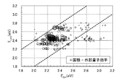

Classifications
-
- H—ELECTRICITY
- H10—SEMICONDUCTOR DEVICES; ELECTRIC SOLID-STATE DEVICES NOT OTHERWISE PROVIDED FOR
- H10K—ORGANIC ELECTRIC SOLID-STATE DEVICES
- H10K50/00—Organic light-emitting devices
- H10K50/10—OLEDs or polymer light-emitting diodes [PLED]
- H10K50/11—OLEDs or polymer light-emitting diodes [PLED] characterised by the electroluminescent [EL] layers
-
- H—ELECTRICITY
- H10—SEMICONDUCTOR DEVICES; ELECTRIC SOLID-STATE DEVICES NOT OTHERWISE PROVIDED FOR
- H10K—ORGANIC ELECTRIC SOLID-STATE DEVICES
- H10K50/00—Organic light-emitting devices
- H10K50/10—OLEDs or polymer light-emitting diodes [PLED]
- H10K50/14—Carrier transporting layers
- H10K50/15—Hole transporting layers
-
- H—ELECTRICITY
- H10—SEMICONDUCTOR DEVICES; ELECTRIC SOLID-STATE DEVICES NOT OTHERWISE PROVIDED FOR
- H10K—ORGANIC ELECTRIC SOLID-STATE DEVICES
- H10K50/00—Organic light-emitting devices
- H10K50/10—OLEDs or polymer light-emitting diodes [PLED]
- H10K50/14—Carrier transporting layers
- H10K50/16—Electron transporting layers
-
- H—ELECTRICITY
- H10—SEMICONDUCTOR DEVICES; ELECTRIC SOLID-STATE DEVICES NOT OTHERWISE PROVIDED FOR
- H10K—ORGANIC ELECTRIC SOLID-STATE DEVICES
- H10K59/00—Integrated devices, or assemblies of multiple devices, comprising at least one organic light-emitting element covered by group H10K50/00
- H10K59/10—OLED displays
- H10K59/12—Active-matrix OLED [AMOLED] displays
-
- H—ELECTRICITY
- H10—SEMICONDUCTOR DEVICES; ELECTRIC SOLID-STATE DEVICES NOT OTHERWISE PROVIDED FOR
- H10K—ORGANIC ELECTRIC SOLID-STATE DEVICES
- H10K59/00—Integrated devices, or assemblies of multiple devices, comprising at least one organic light-emitting element covered by group H10K50/00
- H10K59/30—Devices specially adapted for multicolour light emission
- H10K59/38—Devices specially adapted for multicolour light emission comprising colour filters or colour changing media [CCM]
-
- H—ELECTRICITY
- H10—SEMICONDUCTOR DEVICES; ELECTRIC SOLID-STATE DEVICES NOT OTHERWISE PROVIDED FOR
- H10K—ORGANIC ELECTRIC SOLID-STATE DEVICES
- H10K2101/00—Properties of the organic materials covered by group H10K85/00
- H10K2101/10—Triplet emission
-
- H—ELECTRICITY
- H10—SEMICONDUCTOR DEVICES; ELECTRIC SOLID-STATE DEVICES NOT OTHERWISE PROVIDED FOR
- H10K—ORGANIC ELECTRIC SOLID-STATE DEVICES
- H10K2101/00—Properties of the organic materials covered by group H10K85/00
- H10K2101/20—Delayed fluorescence emission
-
- H—ELECTRICITY
- H10—SEMICONDUCTOR DEVICES; ELECTRIC SOLID-STATE DEVICES NOT OTHERWISE PROVIDED FOR
- H10K—ORGANIC ELECTRIC SOLID-STATE DEVICES
- H10K2101/00—Properties of the organic materials covered by group H10K85/00
- H10K2101/30—Highest occupied molecular orbital [HOMO], lowest unoccupied molecular orbital [LUMO] or Fermi energy values
-
- H—ELECTRICITY
- H10—SEMICONDUCTOR DEVICES; ELECTRIC SOLID-STATE DEVICES NOT OTHERWISE PROVIDED FOR
- H10K—ORGANIC ELECTRIC SOLID-STATE DEVICES
- H10K2101/00—Properties of the organic materials covered by group H10K85/00
- H10K2101/40—Interrelation of parameters between multiple constituent active layers or sublayers, e.g. HOMO values in adjacent layers
-
- H—ELECTRICITY
- H10—SEMICONDUCTOR DEVICES; ELECTRIC SOLID-STATE DEVICES NOT OTHERWISE PROVIDED FOR
- H10K—ORGANIC ELECTRIC SOLID-STATE DEVICES
- H10K2101/00—Properties of the organic materials covered by group H10K85/00
- H10K2101/90—Multiple hosts in the emissive layer
-
- H—ELECTRICITY
- H10—SEMICONDUCTOR DEVICES; ELECTRIC SOLID-STATE DEVICES NOT OTHERWISE PROVIDED FOR
- H10K—ORGANIC ELECTRIC SOLID-STATE DEVICES
- H10K50/00—Organic light-emitting devices
- H10K50/10—OLEDs or polymer light-emitting diodes [PLED]
- H10K50/11—OLEDs or polymer light-emitting diodes [PLED] characterised by the electroluminescent [EL] layers
- H10K50/12—OLEDs or polymer light-emitting diodes [PLED] characterised by the electroluminescent [EL] layers comprising dopants
-
- H—ELECTRICITY
- H10—SEMICONDUCTOR DEVICES; ELECTRIC SOLID-STATE DEVICES NOT OTHERWISE PROVIDED FOR
- H10K—ORGANIC ELECTRIC SOLID-STATE DEVICES
- H10K85/00—Organic materials used in the body or electrodes of devices covered by this subclass
- H10K85/30—Coordination compounds
- H10K85/321—Metal complexes comprising a group IIIA element, e.g. Tris (8-hydroxyquinoline) gallium [Gaq3]
- H10K85/322—Metal complexes comprising a group IIIA element, e.g. Tris (8-hydroxyquinoline) gallium [Gaq3] comprising boron
-
- H—ELECTRICITY
- H10—SEMICONDUCTOR DEVICES; ELECTRIC SOLID-STATE DEVICES NOT OTHERWISE PROVIDED FOR
- H10K—ORGANIC ELECTRIC SOLID-STATE DEVICES
- H10K85/00—Organic materials used in the body or electrodes of devices covered by this subclass
- H10K85/30—Coordination compounds
- H10K85/321—Metal complexes comprising a group IIIA element, e.g. Tris (8-hydroxyquinoline) gallium [Gaq3]
- H10K85/324—Metal complexes comprising a group IIIA element, e.g. Tris (8-hydroxyquinoline) gallium [Gaq3] comprising aluminium, e.g. Alq3
-
- H—ELECTRICITY
- H10—SEMICONDUCTOR DEVICES; ELECTRIC SOLID-STATE DEVICES NOT OTHERWISE PROVIDED FOR
- H10K—ORGANIC ELECTRIC SOLID-STATE DEVICES
- H10K85/00—Organic materials used in the body or electrodes of devices covered by this subclass
- H10K85/60—Organic compounds having low molecular weight
- H10K85/615—Polycyclic condensed aromatic hydrocarbons, e.g. anthracene
- H10K85/622—Polycyclic condensed aromatic hydrocarbons, e.g. anthracene containing four rings, e.g. pyrene
-
- H—ELECTRICITY
- H10—SEMICONDUCTOR DEVICES; ELECTRIC SOLID-STATE DEVICES NOT OTHERWISE PROVIDED FOR
- H10K—ORGANIC ELECTRIC SOLID-STATE DEVICES
- H10K85/00—Organic materials used in the body or electrodes of devices covered by this subclass
- H10K85/60—Organic compounds having low molecular weight
- H10K85/615—Polycyclic condensed aromatic hydrocarbons, e.g. anthracene
- H10K85/624—Polycyclic condensed aromatic hydrocarbons, e.g. anthracene containing six or more rings
-
- H—ELECTRICITY
- H10—SEMICONDUCTOR DEVICES; ELECTRIC SOLID-STATE DEVICES NOT OTHERWISE PROVIDED FOR
- H10K—ORGANIC ELECTRIC SOLID-STATE DEVICES
- H10K85/00—Organic materials used in the body or electrodes of devices covered by this subclass
- H10K85/60—Organic compounds having low molecular weight
- H10K85/615—Polycyclic condensed aromatic hydrocarbons, e.g. anthracene
- H10K85/626—Polycyclic condensed aromatic hydrocarbons, e.g. anthracene containing more than one polycyclic condensed aromatic rings, e.g. bis-anthracene
-
- H—ELECTRICITY
- H10—SEMICONDUCTOR DEVICES; ELECTRIC SOLID-STATE DEVICES NOT OTHERWISE PROVIDED FOR
- H10K—ORGANIC ELECTRIC SOLID-STATE DEVICES
- H10K85/00—Organic materials used in the body or electrodes of devices covered by this subclass
- H10K85/60—Organic compounds having low molecular weight
- H10K85/631—Amine compounds having at least two aryl rest on at least one amine-nitrogen atom, e.g. triphenylamine
- H10K85/633—Amine compounds having at least two aryl rest on at least one amine-nitrogen atom, e.g. triphenylamine comprising polycyclic condensed aromatic hydrocarbons as substituents on the nitrogen atom
-
- H—ELECTRICITY
- H10—SEMICONDUCTOR DEVICES; ELECTRIC SOLID-STATE DEVICES NOT OTHERWISE PROVIDED FOR
- H10K—ORGANIC ELECTRIC SOLID-STATE DEVICES
- H10K85/00—Organic materials used in the body or electrodes of devices covered by this subclass
- H10K85/60—Organic compounds having low molecular weight
- H10K85/631—Amine compounds having at least two aryl rest on at least one amine-nitrogen atom, e.g. triphenylamine
- H10K85/636—Amine compounds having at least two aryl rest on at least one amine-nitrogen atom, e.g. triphenylamine comprising heteroaromatic hydrocarbons as substituents on the nitrogen atom
-
- H—ELECTRICITY
- H10—SEMICONDUCTOR DEVICES; ELECTRIC SOLID-STATE DEVICES NOT OTHERWISE PROVIDED FOR
- H10K—ORGANIC ELECTRIC SOLID-STATE DEVICES
- H10K85/00—Organic materials used in the body or electrodes of devices covered by this subclass
- H10K85/60—Organic compounds having low molecular weight
- H10K85/649—Aromatic compounds comprising a hetero atom
- H10K85/654—Aromatic compounds comprising a hetero atom comprising only nitrogen as heteroatom
-
- H—ELECTRICITY
- H10—SEMICONDUCTOR DEVICES; ELECTRIC SOLID-STATE DEVICES NOT OTHERWISE PROVIDED FOR
- H10K—ORGANIC ELECTRIC SOLID-STATE DEVICES
- H10K85/00—Organic materials used in the body or electrodes of devices covered by this subclass
- H10K85/60—Organic compounds having low molecular weight
- H10K85/649—Aromatic compounds comprising a hetero atom
- H10K85/656—Aromatic compounds comprising a hetero atom comprising two or more different heteroatoms per ring
- H10K85/6565—Oxadiazole compounds
-
- H—ELECTRICITY
- H10—SEMICONDUCTOR DEVICES; ELECTRIC SOLID-STATE DEVICES NOT OTHERWISE PROVIDED FOR
- H10K—ORGANIC ELECTRIC SOLID-STATE DEVICES
- H10K85/00—Organic materials used in the body or electrodes of devices covered by this subclass
- H10K85/60—Organic compounds having low molecular weight
- H10K85/649—Aromatic compounds comprising a hetero atom
- H10K85/657—Polycyclic condensed heteroaromatic hydrocarbons
- H10K85/6572—Polycyclic condensed heteroaromatic hydrocarbons comprising only nitrogen in the heteroaromatic polycondensed ring system, e.g. phenanthroline or carbazole
-
- H—ELECTRICITY
- H10—SEMICONDUCTOR DEVICES; ELECTRIC SOLID-STATE DEVICES NOT OTHERWISE PROVIDED FOR
- H10K—ORGANIC ELECTRIC SOLID-STATE DEVICES
- H10K85/00—Organic materials used in the body or electrodes of devices covered by this subclass
- H10K85/60—Organic compounds having low molecular weight
- H10K85/649—Aromatic compounds comprising a hetero atom
- H10K85/657—Polycyclic condensed heteroaromatic hydrocarbons
- H10K85/6574—Polycyclic condensed heteroaromatic hydrocarbons comprising only oxygen in the heteroaromatic polycondensed ring system, e.g. cumarine dyes
-
- H—ELECTRICITY
- H10—SEMICONDUCTOR DEVICES; ELECTRIC SOLID-STATE DEVICES NOT OTHERWISE PROVIDED FOR
- H10K—ORGANIC ELECTRIC SOLID-STATE DEVICES
- H10K85/00—Organic materials used in the body or electrodes of devices covered by this subclass
- H10K85/60—Organic compounds having low molecular weight
- H10K85/649—Aromatic compounds comprising a hetero atom
- H10K85/657—Polycyclic condensed heteroaromatic hydrocarbons
- H10K85/6576—Polycyclic condensed heteroaromatic hydrocarbons comprising only sulfur in the heteroaromatic polycondensed ring system, e.g. benzothiophene
Description
本発明の一態様は、発光素子、または該発光素子を有する表示装置、電子機器、及び照明装置に関する。 One aspect of the present invention relates to a light emitting element, or a display device, an electronic device, and a lighting device having the light emitting element.
なお、本発明の一態様は、上記の技術分野に限定されない。本明細書等で開示する発明の一態様の技術分野は、物、方法、または、製造方法に関する。または、本発明の一態様は、プロセス、マシン、マニュファクチャ、または、組成物(コンポジション・オブ・マター)に関する。そのため、より具体的に本明細書で開示する本発明の一態様の技術分野としては、半導体装置、表示装置、液晶表示装置、発光装置、照明装置、蓄電装置、記憶装置、それらの駆動方法、または、それらの製造方法、を一例として挙げることができる。 It should be noted that one aspect of the present invention is not limited to the above technical fields. The technical field of one aspect of the invention disclosed in the present specification and the like relates to a product, a method, or a manufacturing method. Alternatively, one aspect of the invention relates to a process, machine, manufacture, or composition (composition of matter). Therefore, more specifically, the technical fields of one aspect of the present invention disclosed in the present specification include semiconductor devices, display devices, liquid crystal display devices, light emitting devices, lighting devices, power storage devices, storage devices, and driving methods thereof. Alternatively, those manufacturing methods can be given as an example.
近年、エレクトロルミネッセンス(Electroluminescence:EL)を利用した発光素子の研究開発が盛んに行われている。これら発光素子の基本的な構成は、一対の電極間に発光性の物質を含む層(EL層)を挟んだ構成である。この素子の電極間に電圧を印加することにより、発光性の物質からの発光が得られる。 In recent years, research and development of light emitting devices using electroluminescence (EL) have been actively carried out. The basic configuration of these light emitting elements is such that a layer (EL layer) containing a light emitting substance is sandwiched between a pair of electrodes. By applying a voltage between the electrodes of this device, light emission from a luminescent substance can be obtained.
上述の発光素子は自発光型であるため、これを用いた表示装置は、視認性に優れ、バックライトが不要であり、消費電力が少ない等の利点を有する。さらに、薄型軽量に作製でき、応答速度が高いなどの利点も有する。 Since the above-mentioned light emitting element is a self-luminous type, a display device using the above-mentioned light emitting element has advantages such as excellent visibility, no backlight, and low power consumption. Further, it can be manufactured thin and lightweight, and has advantages such as high response speed.
発光性の物質に有機化合物を用い、一対の電極間に当該発光性の有機化合物を含むEL層を設けた発光素子(例えば、有機EL素子)の場合、一対の電極間に電圧を印加することにより、陰極から電子が、陽極から正孔(ホール)がそれぞれ発光性のEL層に注入され、電流が流れる。そして、注入された電子及び正孔が再結合することによって発光性の有機化合物が励起状態となり、励起された発光性の有機化合物から発光を得ることができる。 In the case of a light emitting element (for example, an organic EL element) in which an organic compound is used as a luminescent substance and an EL layer containing the luminescent organic compound is provided between a pair of electrodes, a voltage is applied between the pair of electrodes. As a result, electrons are injected from the cathode and holes are injected from the anode into the luminescent EL layer, and a current flows. Then, the injected electrons and holes are recombined to bring the luminescent organic compound into an excited state, and light emission can be obtained from the excited luminescent organic compound.
有機化合物が形成する励起状態の種類としては、一重項励起状態(S*)と三重項励起状態(T*)があり、一重項励起状態からの発光が蛍光、三重項励起状態からの発光が燐光と呼ばれている。また、発光素子におけるそれらの統計的な生成比率は、S*:T*=1:3である。そのため、蛍光を発する化合物(蛍光性化合物)を用いた発光素子より、燐光を発する化合物(燐光性化合物)を用いた発光素子の方が、高い発光効率を得ることが可能となる。したがって、三重項励起状態を発光に変換することが可能な燐光性化合物を用いた発光素子の開発が近年盛んに行われている。 There are two types of excited states formed by organic compounds: singlet excited state (S * ) and triplet excited state (T * ). Emission from the singlet excited state is fluorescence, and emission from the triplet excited state is emission. It is called phosphorescence. Moreover, their statistical generation ratio in the light emitting element is S * : T * = 1: 3. Therefore, a luminous element using a phosphorescent compound (phosphorescent compound) can obtain higher luminous efficiency than a light emitting element using a phosphorescent compound (fluorescent compound). Therefore, in recent years, a light emitting device using a phosphorescent compound capable of converting a triplet excited state into light emission has been actively developed.
燐光性化合物を用いた発光素子のうち、特に青色の発光を呈する発光素子においては、高い三重項励起エネルギー準位を有する安定な化合物の開発が困難であるため、未だ実用化に至っていない。そのため、より安定な蛍光性化合物を用いた発光素子の開発が行われており、蛍光性化合物を用いた発光素子(蛍光発光素子)の発光効率を高める手法が探索されている。 Among the light emitting elements using phosphorescent compounds, particularly in the light emitting element exhibiting blue light emission, it is difficult to develop a stable compound having a high triplet excitation energy level, so that it has not been put into practical use yet. Therefore, a light emitting element using a more stable fluorescent compound has been developed, and a method for increasing the luminous efficiency of the light emitting element (fluorescent light emitting element) using the fluorescent compound is being sought.
三重項励起状態の一部を発光に変換することが可能な材料として、熱活性化遅延蛍光(Thermally Activated Delayed Fluorescence:TADF)体が知られている。熱活性化遅延蛍光体では、三重項励起状態から逆項間交差により一重項励起状態が生成され、一重項励起状態から発光に変換される。 As a material capable of converting a part of the triplet excited state into light emission, a Thermally Activated Fluorescence (TADF) body is known. In a thermal activated delayed fluorescent state, a singlet excited state is generated from a triplet excited state by an intersystem crossing, and the singlet excited state is converted into light emission.
熱活性化遅延蛍光体を用いた発光素子において、発光効率を高めるためには、熱活性化遅延蛍光体において、三重項励起状態から一重項励起状態が効率よく生成するだけでなく、一重項励起状態から効率よく発光が得られること、すなわち蛍光量子収率が高いことが重要となる。 In order to improve the emission efficiency of a thermally activated delayed fluorescent element, not only is the triplet excited state efficiently generated from the triplet excited state, but also the singlet excited state is efficiently generated. It is important that light emission can be efficiently obtained from the state, that is, the fluorescence quantum yield is high.
2種類の有機化合物で形成される励起錯体は、一重項励起状態と三重項励起状態のエネルギー差が小さくなるため、当該励起錯体を熱活性化遅延蛍光体として用いる方法が提案されている(例えば、特許文献1参照)。 Since the energy difference between the singlet excited state and the triplet excited state of the excited complex formed by the two kinds of organic compounds is small, a method of using the excited complex as a thermal activated delayed fluorescent substance has been proposed (for example). , Patent Document 1).
また、熱活性化遅延蛍光体と、蛍光性化合物と、を有する発光素子において、熱活性化遅延蛍光体の一重項励起エネルギーを、蛍光性化合物へと移動させ、当該蛍光性化合物から発光を得る方法が提案されている(例えば、特許文献2参照)。 Further, in a light emitting element having a thermally activated delayed fluorescent substance and a fluorescent compound, the singlet excitation energy of the thermally activated delayed fluorescent substance is transferred to the fluorescent compound to obtain light emission from the fluorescent compound. A method has been proposed (see, for example, Patent Document 2).
熱活性化遅延蛍光体を有する発光素子において、発光効率を高めるためには、三重項励起状態から一重項励起状態が効率よく生成することが好ましい。しかしながら、熱活性化遅延蛍光体として励起錯体を用いる場合、発光効率を高めるための手段は明らかになっていない。 In a light emitting element having a thermally activated delayed fluorescent substance, it is preferable to efficiently generate a singlet excited state from a triplet excited state in order to increase the luminous efficiency. However, when an excited complex is used as the thermally activated delayed fluorescent substance, the means for increasing the luminous efficiency has not been clarified.
また、熱活性化遅延蛍光体と蛍光性化合物とを有する発光素子において、発光効率を高めるためには、熱活性化遅延蛍光体の一重項励起状態から蛍光性化合物の一重項励起状態へ、効率よくエネルギーが移動することが好ましい。また、熱活性化遅延蛍光体の三重項励起状態から蛍光性化合物の三重項励起状態へのエネルギー移動を抑制することが好ましい。そのためには、当該熱活性化遅延蛍光体の発光効率が高いことが好ましいが、熱活性化遅延蛍光体として励起錯体を用いる場合、励起錯体の発光効率を高める手段は明らかになっていない。 Further, in a light emitting element having a thermally activated delayed fluorescent substance and a fluorescent compound, in order to increase the light emission efficiency, the efficiency is changed from the singlet excited state of the thermally activated delayed fluorescent substance to the singlet excited state of the fluorescent compound. It is preferable that energy is transferred well. Further, it is preferable to suppress the energy transfer from the triplet excited state of the thermally activated delayed fluorescent substance to the triplet excited state of the fluorescent compound. For that purpose, it is preferable that the luminous efficiency of the thermally activated delayed fluorescent substance is high, but when an excited complex is used as the thermally activated delayed fluorescent substance, a means for increasing the luminous efficiency of the excited complex has not been clarified.
したがって、本発明の一態様では、発光効率が高い発光素子を提供することを課題の一とする。または、本発明の一態様では、消費電力が低減された発光素子を提供することを課題の一とする。または、本発明の一態様では、新規な発光素子を提供することを課題の一とする。または、本発明の一態様では、新規な発光装置を提供することを課題の一とする。または、本発明の一態様では、新規な表示装置を提供することを課題の一とする。 Therefore, in one aspect of the present invention, one of the problems is to provide a light emitting element having high luminous efficiency. Alternatively, in one aspect of the present invention, one of the problems is to provide a light emitting element having reduced power consumption. Alternatively, in one aspect of the present invention, it is an object of the present invention to provide a novel light emitting device. Alternatively, one aspect of the present invention is to provide a novel light emitting device. Alternatively, one aspect of the present invention is to provide a new display device.
なお、上記の課題の記載は、他の課題の存在を妨げない。なお、本発明の一態様は、必ずしも、これらの課題の全てを解決する必要はない。上記以外の課題は、明細書等の記載から自ずと明らかであり、明細書等の記載から上記以外の課題を抽出することが可能である。 The description of the above problem does not prevent the existence of other problems. It should be noted that one aspect of the present invention does not necessarily have to solve all of these problems. Issues other than the above are self-evident from the description of the specification and the like, and it is possible to extract problems other than the above from the description of the specification and the like.
本発明の一態様は、励起錯体を形成する組み合わせの2種類の有機化合物を有する発光素子である。 One aspect of the present invention is a light emitting device having two kinds of organic compounds in a combination forming an excitation complex.
また、本発明の一態様は、第1の有機化合物と、第2の有機化合物と、を有する発光素子であって、第1の有機化合物と、第2の有機化合物と、が励起錯体を形成する組み合わせであり、第1の有機化合物の最低三重項励起エネルギー準位または第2の有機化合物の最低三重項励起エネルギー準位のうちエネルギーが低い一方は、励起錯体が呈する発光のエネルギーの-0.2eV以上0.4eV以下のエネルギーを有する発光素子である。 Further, one aspect of the present invention is a light emitting element having a first organic compound and a second organic compound, wherein the first organic compound and the second organic compound form an excitation complex. Of the lowest triple-term excitation energy level of the first organic compound or the lowest triple-term excitation energy level of the second organic compound, the one with the lower energy is the emission energy of -0 exhibited by the excitation complex. It is a light emitting element having an energy of .2 eV or more and 0.4 eV or less.
また、本発明の他の一態様は、第1の有機化合物と、第2の有機化合物と、を有する発光素子であって、第1の有機化合物と、第2の有機化合物と、が励起錯体を形成する組み合わせであり、第1の有機化合物のLUMO準位と第2の有機化合物のHOMO準位とのエネルギー差は、励起錯体が呈する発光のエネルギーの-0.1eV以上0.4eV以下である、発光素子である。 Further, another aspect of the present invention is a light emitting element having a first organic compound and a second organic compound, wherein the first organic compound and the second organic compound are excited complexes. The energy difference between the LUMO level of the first organic compound and the HOMO level of the second organic compound is −0.1 eV or more and 0.4 eV or less of the emission energy exhibited by the excited complex. There is a light emitting element.
また、本発明の他の一態様は、第1の有機化合物と、第2の有機化合物と、を有する発光素子であって、第1の有機化合物と、第2の有機化合物と、が励起錯体を形成する組み合わせであり、第1の有機化合物のLUMO準位と第2の有機化合物のHOMO準位とのエネルギー差は、励起錯体が呈する発光のエネルギーの-0.1eV以上0.4eV以下であり、第1の有機化合物の最低三重項励起エネルギー準位または第2の有機化合物の最低三重項励起エネルギー準位のうちエネルギーが低い一方は、励起錯体が呈する発光のエネルギーの-0.2eV以上0.4eV以下のエネルギーを有する発光素子である。 Further, another aspect of the present invention is a light emitting element having a first organic compound and a second organic compound, wherein the first organic compound and the second organic compound are excited complexes. The energy difference between the LUMO level of the first organic compound and the HOMO level of the second organic compound is -0.1 eV or more and 0.4 eV or less of the emission energy exhibited by the excited complex. There, one of the lowest triple-term excitation energy levels of the first organic compound or the lowest triple-term excitation energy level of the second organic compound, whichever has the lower energy, is -0.2 eV or more of the emission energy exhibited by the excitation complex. It is a light emitting element having an energy of 0.4 eV or less.
上記各構成において、発光素子は、さらにゲスト材料を有し、ゲスト材料は、発光を呈する機能を有し、励起錯体は、ゲスト材料へ励起エネルギーを供与する機能を有すると好ましい。また、ゲスト材料は、蛍光性化合物を有し、励起錯体が呈する発光スペクトルが、ゲスト材料の最も低いエネルギー側の吸収帯と重なる領域を有すると好ましい。 In each of the above configurations, it is preferable that the light emitting device further has a guest material, the guest material has a function of exhibiting light emission, and the excitation complex has a function of supplying excitation energy to the guest material. Further, it is preferable that the guest material has a fluorescent compound and has a region in which the emission spectrum exhibited by the excitation complex overlaps with the absorption band on the lowest energy side of the guest material.
また、上記各構成において、第1の有機化合物は、電子を輸送する機能を有し、第2の有機化合物は、正孔を輸送する機能を有すると好ましい。また、第1の有機化合物は、π電子不足型複素芳香環骨格を有し、第2の有機化合物は、π電子過剰型複素芳香環骨格または芳香族アミン骨格の少なくとも一方を有すると好ましい。また、第1の有機化合物は、ジアジン骨格を有し、第2の有機化合物は、カルバゾール骨格およびトリアリールアミン骨格を有すると好ましい。 Further, in each of the above configurations, it is preferable that the first organic compound has a function of transporting electrons and the second organic compound has a function of transporting holes. Further, it is preferable that the first organic compound has a π-electron-deficient heteroaromatic ring skeleton, and the second organic compound has at least one of a π-electron-rich heteroaromatic ring skeleton or an aromatic amine skeleton. Further, it is preferable that the first organic compound has a diazine skeleton and the second organic compound has a carbazole skeleton and a triarylamine skeleton.
また、本発明の他の一態様は、上記各構成の発光素子と、カラーフィルタまたはトランジスタの少なくとも一方と、を有する表示装置である。また、本発明の他の一態様は、当該表示装置と、筐体またはタッチセンサの少なくとも一方と、を有する電子機器である。また、本発明の他の一態様は、上記各構成の発光素子と、筐体またはタッチセンサの少なくとも一方と、を有する照明装置である。また、本発明の一態様は、発光素子を有する発光装置だけでなく、発光装置を有する電子機器も範疇に含める。従って、本明細書中における発光装置とは、画像表示デバイス、もしくは光源(照明装置含む)を指す。また、発光素子にコネクター、例えばFPC(Flexible Printed Circuit)、TCP(Tape Carrier Package)が取り付けられた表示モジュール、TCPの先にプリント配線板が設けられた表示モジュール、または発光素子にCOG(Chip On Glass)方式によりIC(集積回路)が直接実装された表示モジュールも発光装置に含む場合がある。 Further, another aspect of the present invention is a display device having a light emitting element having each of the above configurations and at least one of a color filter or a transistor. Further, another aspect of the present invention is an electronic device having the display device and at least one of a housing or a touch sensor. Further, another aspect of the present invention is a lighting device having a light emitting element having each of the above configurations and at least one of a housing or a touch sensor. Further, one aspect of the present invention includes not only a light emitting device having a light emitting element but also an electronic device having a light emitting device. Therefore, the light emitting device in the present specification refers to an image display device or a light source (including a lighting device). Further, a display module in which a connector such as an FPC (Flexible Printed Circuit) or TCP (Tape Carrier Package) is attached to the light emitting element, a display module in which a printed wiring board is provided at the end of the TCP, or a COG (Chip On) in the light emitting element. A display module in which an IC (integrated circuit) is directly mounted by the Glass) method may also be included in the light emitting device.
本発明の一態様により、発光効率が高い発光素子を提供することができる。または、本発明の一態様により、消費電力が低減された発光素子を提供することができる。または、本発明の一態様により、新規な発光素子を提供することができる。または、本発明の一態様により、新規な発光装置を提供することができる。または、本発明の一態様により、新規な表示装置を提供することができる。 According to one aspect of the present invention, it is possible to provide a light emitting device having high luminous efficiency. Alternatively, according to one aspect of the present invention, it is possible to provide a light emitting element having reduced power consumption. Alternatively, according to one aspect of the present invention, a novel light emitting device can be provided. Alternatively, according to one aspect of the present invention, a novel light emitting device can be provided. Alternatively, according to one aspect of the present invention, a new display device can be provided.
なお、これらの効果の記載は、他の効果の存在を妨げない。なお、本発明の一態様は、必ずしも、これらの効果の全てを有する必要はない。なお、これら以外の効果は、明細書、図面、請求項などの記載から、自ずと明らかであり、明細書、図面、請求項などの記載から、これら以外の効果を抽出することが可能である。 The description of these effects does not preclude the existence of other effects. It should be noted that one aspect of the present invention does not necessarily have to have all of these effects. It should be noted that the effects other than these are naturally clear from the description of the description, drawings, claims and the like, and it is possible to extract the effects other than these from the description of the description, drawings, claims and the like.
以下、本発明の実施の態様について図面を用いて詳細に説明する。但し、本発明は以下の説明に限定されず、本発明の趣旨及びその範囲から逸脱することなくその形態及び詳細を様々に変更し得ることが可能である。従って、本発明は以下に示す実施の形態の記載内容に限定して解釈されない。 Hereinafter, embodiments of the present invention will be described in detail with reference to the drawings. However, the present invention is not limited to the following description, and its form and details can be variously changed without departing from the spirit and scope of the present invention. Therefore, the present invention is not construed as being limited to the description of the embodiments shown below.
なお、図面等において示す各構成の、位置、大きさ、範囲などは、理解の簡単のため、実際の位置、大きさ、範囲などを表していない場合がある。このため、開示する発明は、必ずしも、図面等に開示された位置、大きさ、範囲などに限定されない。 The position, size, range, etc. of each configuration shown in the drawings may not represent the actual position, size, range, etc. for the sake of easy understanding. Therefore, the disclosed invention is not necessarily limited to the position, size, range, etc. disclosed in the drawings and the like.
また、本明細書等において、第1、第2等として付される序数詞は便宜上用いており、工程順又は積層順を示さない場合がある。そのため、例えば、「第1の」を「第2の」又は「第3の」などと適宜置き換えて説明することができる。また、本明細書等に記載されている序数詞と、本発明の一態様を特定するために用いられる序数詞は一致しない場合がある。 Further, in the present specification and the like, the ordinal numbers attached as the first, second, etc. are used for convenience, and may not indicate the process order or the stacking order. Therefore, for example, the "first" can be appropriately replaced with the "second" or "third" for explanation. In addition, the ordinal numbers described in the present specification and the like may not match the ordinal numbers used to specify one aspect of the present invention.
また、本明細書等において、図面を用いて発明の構成を説明するにあたり、同じものを指す符号は異なる図面間でも共通して用いる場合がある。 Further, in the present specification and the like, when explaining the structure of the invention by using the drawings, the reference numerals indicating the same may be commonly used between different drawings.
また、本明細書等において、「膜」という用語と、「層」という用語とは、互いに入れ替えることが可能である。例えば、「導電層」という用語を、「導電膜」という用語に変更することが可能な場合がある。または、例えば、「絶縁膜」という用語を、「絶縁層」という用語に変更することが可能な場合がある。 Further, in the present specification and the like, the term "membrane" and the term "layer" can be interchanged with each other. For example, it may be possible to change the term "conductive layer" to the term "conductive layer". Alternatively, for example, it may be possible to change the term "insulating film" to the term "insulating layer".
また、本明細書等において、一重項励起状態(S*)は、励起エネルギーを有する一重項状態のことである。また、S1準位は一重項励起エネルギー準位の最も低い準位であり、最も低い一重項励起状態(S1状態)の励起エネルギー準位のことである。また、三重項励起状態(T*)は、励起エネルギーを有する三重項状態のことである。また、T1準位は、三重項励起エネルギー準位の最も低い準位であり、最も低い三重項励起状態(T1状態)の励起エネルギー準位のことである。なお、本明細書等において、単に一重項励起状態および一重項励起エネルギー準位と表記した場合であっても、S1状態およびS1準位を表す場合がある。また、三重項励起状態および三重項励起エネルギー準位と表記した場合であっても、T1状態およびT1準位を表す場合がある。 Further, in the present specification and the like, the singlet excited state (S * ) is a singlet state having excitation energy. Further, the S1 level is the lowest level of the singlet excited energy level, and is the excited energy level of the lowest singlet excited state (S1 state). The triplet excited state (T * ) is a triplet state having excitation energy. The T1 level is the lowest level of the triplet excited energy level, and is the excited energy level of the lowest triplet excited state (T1 state). In addition, in this specification and the like, even if it is simply described as a singlet excited state and a singlet excited energy level, it may represent an S1 state and an S1 level. Further, even when the triplet excited state and the triplet excited energy level are described, they may represent the T1 state and the T1 level.
また、本明細書等において蛍光性化合物とは、一重項励起状態から基底状態へ緩和する際に可視光領域に発光を与える化合物である。燐光性化合物とは、三重項励起状態から基底状態へ緩和する際に、室温において可視光領域に発光を与える化合物である。換言すると燐光性化合物とは、三重項励起エネルギーを可視光へ変換可能な化合物の一つである。 Further, in the present specification and the like, the fluorescent compound is a compound that gives light to the visible light region when the singlet excited state is relaxed to the ground state. The phosphorescent compound is a compound that emits light in the visible light region at room temperature when the triplet excited state is relaxed to the ground state. In other words, a phosphorescent compound is one of the compounds capable of converting triplet excitation energy into visible light.
なお、本明細書等において、室温とは、0℃以上40℃以下のいずれかの温度をいう。 In the present specification and the like, room temperature means any temperature of 0 ° C. or higher and 40 ° C. or lower.
また、本明細書等において、青色の波長領域は、400nm以上490nm未満であり、青色の発光は、該波長領域に少なくとも一つの発光スペクトルピークを有する。また、緑色の波長領域は、490nm以上580nm未満であり、緑色の発光は、該波長領域に少なくとも一つの発光スペクトルピークを有する。また、赤色の波長領域は、580nm以上680nm以下であり、赤色の発光は、該波長領域に少なくとも一つの発光スペクトルピークを有する。 Further, in the present specification and the like, the blue wavelength region is 400 nm or more and less than 490 nm, and the blue emission has at least one emission spectrum peak in the wavelength region. Further, the green wavelength region is 490 nm or more and less than 580 nm, and the green emission has at least one emission spectrum peak in the wavelength region. Further, the red wavelength region is 580 nm or more and 680 nm or less, and the red emission has at least one emission spectrum peak in the wavelength region.
(実施の形態1)
本実施の形態では、本発明の一態様の発光素子について、図1乃至図3を用いて以下説明する。
(Embodiment 1)
In the present embodiment, the light emitting device of one aspect of the present invention will be described below with reference to FIGS. 1 to 3.
<発光素子の構成例1>
まず、本発明の一態様の発光素子の構成について、図1(A)及び(B)を用いて、以下説明する。
<Structure example 1 of light emitting element>
First, the configuration of the light emitting device according to one aspect of the present invention will be described below with reference to FIGS. 1 (A) and 1 (B).
図1(A)は、本発明の一態様の発光素子450の断面模式図である。
FIG. 1A is a schematic cross-sectional view of a
発光素子450は、一対の電極(電極401及び電極402)を有し、該一対の電極間に設けられたEL層400を有する。EL層400は、少なくとも発光層430を有する。
The
また、図1(A)に示すEL層400は、発光層430の他に、正孔注入層411、正孔輸送層412、電子輸送層418、及び電子注入層419等の機能層を有する。
Further, the
なお、本実施の形態においては、一対の電極のうち、電極401を陽極として、電極402を陰極として説明するが、発光素子450の構成としては、その限りではない。つまり、電極401を陰極とし、電極402を陽極とし、当該電極間の各層の積層を、逆の順番にしてもよい。すなわち、陽極側から、正孔注入層411と、正孔輸送層412と、発光層430と、電子輸送層418と、電子注入層419と、が積層する順番とすればよい。
In the present embodiment, of the pair of electrodes, the
なお、EL層400の構成は、図1(A)に示す構成に限定されず、正孔注入層411、正孔輸送層412、電子輸送層418、及び電子注入層419の中から選ばれた少なくとも一つを有する構成とすればよい。あるいは、EL層400は、正孔または電子の注入障壁を低減する、正孔または電子の輸送性を向上する、正孔または電子の輸送性を阻害する、または電極による消光現象を抑制する、ことができる等の機能を有する機能層を有する構成としてもよい。なお、機能層はそれぞれ単層であっても、複数の層が積層された構成であってもよい。
The configuration of the
図1(B)は、図1(A)に示す発光層430の一例を示す断面模式図である。図1(B)に示す発光層430は、有機化合物431と、有機化合物432と、を有する。
FIG. 1B is a schematic cross-sectional view showing an example of the
本発明の一態様の発光素子450においては、一対の電極(電極401及び電極402)間に電圧を印加することにより、陰極から電子が、陽極から正孔(ホール)が、それぞれEL層400に注入され、電流が流れる。そして、注入された電子及び正孔が再結合することによって、励起子が形成される。キャリア(電子および正孔)の再結合によって生じる励起子のうち、一重項励起子と三重項励起子の比(以下、励起子生成確率)は、統計的確率により、1:3となる。そのため、蛍光性の発光素子において、発光に寄与する一重項励起子が生成する割合は25%であり、発光に寄与しない三重項励起子が生成する割合は75%となる。したがって、発光に寄与しない三重項励起子を、発光に寄与する一重項励起子へ変換することが、発光素子の発光効率を向上させるためには重要である。
In the
<発光素子の発光機構1>
次に、発光層430の発光機構について、以下説明を行う。
<Light emitting mechanism of light emitting
Next, the light emitting mechanism of the
発光層430が有する有機化合物431および有機化合物432は、励起錯体(エキサイプレックス、エキシプレックスまたはExciplexともいう)を形成する組み合わせであると好ましい。
The
有機化合物431と有機化合物432との組み合わせは、励起錯体を形成することが可能な組み合わせであればよいが、一方が正孔を輸送する機能(正孔輸送性)を有する化合物であり、他方が電子を輸送する機能(電子輸送性)を有する化合物であることが、より好ましい。この場合、ドナー-アクセプター型の励起錯体を形成しやすくなり、効率よく励起錯体を形成することができる。また、有機化合物431と有機化合物432との組み合わせが、正孔輸送性を有する化合物と電子輸送性を有する化合物との組み合わせである場合、その混合比によってキャリアバランスを容易に制御することが可能となる。具体的には、正孔輸送性を有する化合物:電子輸送性を有する化合物=1:9から9:1(重量比)の範囲が好ましい。また、該構成を有することで、容易にキャリアバランスを制御することができることから、キャリア再結合領域の制御も簡便に行うことができる。
The combination of the
また、効率よく励起錯体を形成するホスト材料の組み合わせとしては、有機化合物431及び有機化合物432のうち一方のHOMO(Highest Occupied Molecular Orbital、最高被占軌道ともいう)準位が他方のHOMO準位より高く、一方のLUMO(Lowest Unoccupied Molecular Orbital、最低空軌道ともいう)準位が他方のLUMO準位より高いことが好ましい。
As a combination of host materials that efficiently form an excitation complex, the HOMO (Highest Occupied Molecular Orbital) level of one of the
例えば、有機化合物431が電子輸送性を有し、有機化合物432が正孔輸送性を有する場合、図2(A)に示すエネルギーバンド図のように、有機化合物432のHOMO準位が有機化合物431のHOMO準位より高いことが好ましく、有機化合物432のLUMO準位が有機化合物431のLUMO準位より高いことが好ましい。具体的には、有機化合物431のHOMO準位と有機化合物432のHOMO準位とのエネルギー差は、好ましくは0.05eV以上であり、より好ましくは0.1eV以上であり、さらに好ましくは0.2eV以上である。また、有機化合物431のLUMO準位と有機化合物432のLUMO準位とのエネルギー差は、好ましくは0.05eV以上であり、より好ましくは0.1eV以上であり、さらに好ましくは0.2eV以上である。該エネルギー差を有することで、一対の電極(電極401および電極402)から注入されたキャリアである電子及び正孔が、有機化合物431および有機化合物432に、それぞれ注入されやすくなり好適である。
For example, when the
なお、図2(A)において、Host(431)は有機化合物431を表し、Host(432)は有機化合物432を表し、ΔEH1は有機化合物431のLUMO準位とHOMO準位とのエネルギー差を表し、ΔEH2は有機化合物432のLUMO準位とHOMO準位とのエネルギー差を表し、ΔEEは有機化合物431のLUMO準位と有機化合物432のHOMO準位とのエネルギー差を表す、表記及び符号である。
In FIG. 2A, Host (431) represents the
また、このとき、有機化合物431と有機化合物432とが形成する励起錯体は、有機化合物431にLUMOの分子軌道を有し、有機化合物432にHOMOの分子軌道を有する励起錯体となる。また、該励起錯体の励起エネルギーは、有機化合物431のLUMO準位と有機化合物432のHOMO準位とのエネルギー差(ΔEE)に概ね相当し、有機化合物431のLUMO準位とHOMO準位とのエネルギー差(ΔEH1)及び有機化合物432のLUMO準位とHOMO準位とのエネルギー差(ΔEH2)より小さくなる。したがって、有機化合物431と有機化合物432とが励起錯体を形成することで、より低い励起エネルギーで励起状態を形成することが可能となる。また、より低い励起エネルギーを有するため、該励起錯体は、安定な励起状態を形成することができる。
Further, at this time, the excitation complex formed by the
また、発光層430における有機化合物431と、有機化合物432とのエネルギー準位の相関を図2(B)に示す。なお、図2(B)における表記及び符号は、以下の通りである。
・Host(431):有機化合物431
・Host(432):有機化合物432
・SH1:有機化合物431のS1準位
・TH1:有機化合物431のT1準位
・SH2:有機化合物432のS1準位
・TH2:有機化合物432のT1準位
・SE:励起錯体のS1準位
・TE:励起錯体のT1準位
Further, FIG. 2B shows the correlation between the energy levels of the
Host (431):
Host (432):
・SH1 : S1 level of
本発明の一態様の発光素子においては、発光層430が有する有機化合物431と有機化合物432とが励起錯体を形成する。励起錯体のS1準位(SE)と励起錯体のT1準位(TE)とは、互いに隣接したエネルギー準位となる(図2(B) ルートE1参照)。
In the light emitting element of one aspect of the present invention, the
励起錯体は、2種類の物質からなる励起状態であり、光励起の場合、励起状態となった一方の物質が基底状態である他方の物質と相互作用することによって形成される。そして、光を発することによって基底状態になると、励起錯体を形成していた2種類の物質は、また元の別々の物質として振る舞う。電気励起の場合は、一方が励起状態になると、速やかに他方と相互作用することで励起錯体を形成する。あるいは、一方が正孔を、他方が電子を受け取ることで速やかに励起錯体を形成することができる。この場合、いずれの物質においても励起状態を形成することなく励起錯体を形成することができるため、発光層430における励起子のほとんどが励起錯体として存在することが可能となる。励起錯体の励起エネルギー準位(SEおよびTE)は、励起錯体を形成する各有機化合物(有機化合物431および有機化合物432)のS1準位(SH1およびSH2)より低くなるため、より低い励起エネルギーで有機化合物431の励起状態を形成することが可能となる。これによって、発光素子450の駆動電圧を低減することができる。
The excited complex is an excited state composed of two kinds of substances, and in the case of photoexcitation, it is formed by interacting with one substance in the excited state with the other substance in the ground state. Then, when the ground state is reached by emitting light, the two kinds of substances forming the excited complex also behave as the original separate substances. In the case of electrical excitation, when one is excited, it quickly interacts with the other to form an excited complex. Alternatively, an excited complex can be rapidly formed by receiving holes on one side and electrons on the other side. In this case, since the excited complex can be formed in any substance without forming an excited state, most of the excitons in the
励起錯体のS1準位(SE)とT1準位(TE)は、互いに隣接したエネルギー準位であるため、熱活性化遅延蛍光を呈する機能を有する。すなわち、励起錯体は三重項励起エネルギーを逆項間交差(アップコンバージョン)によって一重項励起エネルギーに変換する機能を有する(図2(B) ルートE2参照)。したがって、発光層430で生成した三重項励起エネルギーの一部は励起錯体により一重項励起エネルギーに変換される。そのためには、励起錯体のS1準位(SE)とT1準位(TE)とのエネルギー差は、0eVより大きく0.2eV以下であると好ましく、0eVより大きく0.1eV以下であるとより好ましい。なお、逆項間交差を効率よく生じさせるためには、励起錯体のT1準位(TE)が、励起錯体を形成する各有機化合物(有機化合物431および有機化合物432)のT1準位(TH1およびTH2)よりも低いことが好ましい。これにより、各有機化合物による励起錯体の三重項励起エネルギーのクエンチが生じにくくなり、効率よく逆項間交差が発生する。
Since the S1 level ( SE ) and the T1 level ( TE ) of the excited complex are energy levels adjacent to each other, they have a function of exhibiting thermal activated delayed fluorescence. That is, the excitation complex has a function of converting triplet excitation energy into singlet excitation energy by intersystem crossing (up-conversion) (see Route E2 in FIG . 2B). Therefore, a part of the triplet excitation energy generated in the
また、キャリアの再結合によって直接および逆項間交差を経て生成した一重項励起状態の励起錯体から、発光が得られる。なお、励起錯体が呈する発光のエネルギー(略称:ΔEEm)は、励起錯体のS1準位(SE)のエネルギーに相当するが、励起錯体のLUMO準位とHOMO準位とのエネルギー差(ΔEE)と同等か、それよりも小さくなる(ΔEE≧ΔEEm)。このとき、励起錯体を形成する各有機化合物(有機化合物431および有機化合物432)のT1準位(TH1およびTH2)のうちエネルギーが低い一方のエネルギーが、励起錯体が呈する発光のエネルギー(ΔEEm)の-0.2eV以上、好ましくは0eV以上のエネルギーであれば、有機化合物431と有機化合物432とで形成する励起錯体から効率よく発光を得ることができることを本発明者は見出した。これにより、各有機化合物による励起錯体の三重項励起エネルギーのクエンチが生じにくくなり、効率よく逆項間交差が発生する。
In addition, emission is obtained from the excited complex in the singlet excited state generated through direct and inverse intersystem crossing by carrier recombination. The emission energy (abbreviation: ΔE Em ) exhibited by the excited complex corresponds to the energy of the S1 level (SE) of the excited complex, but the energy difference ( ΔE ) between the LUMO level and the HOMO level of the excited complex. E ) equal to or less than (ΔE E ≧ ΔE Em ). At this time, one of the lower energies of the T1 levels ( TH1 and TH2 ) of each organic compound (
なお、発光のエネルギーは、発光スペクトルの最も短波長側の発光ピーク(極大値、またはショルダーを含む)の波長から導出することができる。 The emission energy can be derived from the wavelength of the emission peak (including the maximum value or the shoulder) on the shortest wavelength side of the emission spectrum.
また、各有機化合物(有機化合物431および有機化合物432)のT1準位(TH1およびTH2)が励起錯体のT1準位(TE)より十分に大きいとき、各有機化合物(有機化合物431および有機化合物432)のT1準位(TH1及びTH2)およびS1準位(SH1およびSH2)の双方が大きな励起エネルギーを有することになり、各有機化合物(有機化合物431および有機化合物432)のLUMO準位とHOMO準位とのエネルギー差(ΔEH1およびΔEH2)も大きくなる。そうすると、有機化合物431および有機化合物432へのキャリア(電子および正孔)の注入が困難となるため、結果として、励起錯体が形成されにくくなってしまう。また、有機化合物431または有機化合物432の一方でキャリア再結合が生じ、他方と励起錯体を形成する場合に、有機化合物431および有機化合物432が大きな励起エネルギーを有すると、有機化合物431および有機化合物432の励起エネルギーと、励起錯体の励起エネルギーと、のエネルギー差が大きくなるため、励起錯体を形成する際に該エネルギー差に相当するエネルギーを放出する無輻射失活過程を経る必要があり、分子の立体構造における構造緩和が大きくなる。有機化合物431の励起状態または有機化合物432の励起状態と、励起錯体と、の分子の立体構造が大きく異なると、励起錯体を形成する反応の速度定数は小さくなるため、励起錯体が形成されにくくなってしまう。そのため、励起錯体を形成する各有機化合物(有機化合物431および有機化合物432)のT1準位(TH1およびTH2)のうち少なくともエネルギーが低い一方のエネルギーと、励起錯体が呈する発光のエネルギー(ΔEEm)とのエネルギー差は小さい方が好ましく、具体的には励起錯体を形成する各有機化合物(有機化合物431および有機化合物432)のT1準位(TH1およびTH2)のうちエネルギーが低い一方のエネルギーと、励起錯体が呈する発光のエネルギー(ΔEEm)とのエネルギー差は0.4eV以下であると好ましい。
Further, when the T1 level ( TH1 and TH2 ) of each organic compound (
以上の理由から、励起錯体を形成する各有機化合物(有機化合物431および有機化合物432)のT1準位(TH1およびTH2)のうちエネルギーが低い一方のエネルギーが、励起錯体が呈する発光のエネルギー(ΔEEm)の-0.2eV以上0.4eV以下のエネルギーであると好ましく、0eV以上0.4eV以下のエネルギーであるとより好ましい。
For the above reasons, the energy of one of the lower energies of the T1 levels ( TH1 and TH2 ) of each organic compound (
また、有機化合物431のLUMO準位と有機化合物432のHOMO準位とのエネルギー差(ΔEE)は、これらが形成する励起錯体の発光のエネルギー(ΔEEm)と同等かそれ以上のエネルギーを有する(ΔEE≧ΔEEm)が、励起状態である励起錯体(有機化合物431および有機化合物432)の分子の立体構造と、基底状態の有機化合物431および有機化合物432の分子の立体構造とで、立体構造が大きく異なる場合、励起錯体の発光過程において分子の立体構造の構造緩和が大きくなり、ΔEEとΔEEmとのエネルギー差が大きくなる。このとき、励起錯体の発光の速度定数は小さくなるため、励起錯体の発光効率が低下する場合がある。したがって、有機化合物431のLUMO準位と有機化合物432のHOMO準位とのエネルギー差(ΔEE)と、これらが形成する励起錯体の発光のエネルギー(ΔEEm)と、のエネルギー差は小さいことが好ましい。具体的には、有機化合物431のLUMO準位と有機化合物432のHOMO準位とのエネルギー差(ΔEE)は、これらが形成する励起錯体の発光のエネルギー(ΔEEm)の-0.1eV以上0.4eV以下のエネルギー(ΔEEm-0.1eV≦ΔEE≦ΔEEm+0.4eV)であると好ましく、0eV以上0.4eV以下のエネルギー(ΔEEm≦ΔEE≦ΔEEm+0.4eV)であるとより好ましい。
Further, the energy difference (ΔE E ) between the LUMO level of the
なお、有機化合物のLUMO準位およびHOMO準位は、サイクリックボルタンメトリ(CV)測定によって測定される有機化合物の電気化学特性(還元電位および酸化電位)から導出することができる。
<発光素子の構成例2>
The LUMO level and the HOMO level of the organic compound can be derived from the electrochemical properties (reduction potential and oxidation potential) of the organic compound measured by cyclic voltammetry (CV) measurement.
<Structure example 2 of light emitting element>
次に、図1(B)に示す発光層と異なる構成例について、図3(A)を用いて、以下説明を行う。 Next, a configuration example different from the light emitting layer shown in FIG. 1 (B) will be described below with reference to FIG. 3 (A).
図3(A)は、図1(A)に示す発光層430の一例を示す断面模式図である。図3(A)に示す発光層430は、有機化合物431と、有機化合物432と、ゲスト材料433と、を有する。
FIG. 3A is a schematic cross-sectional view showing an example of the
なお、ゲスト材料433としては、発光性の有機化合物を用いればよく、該発光性の有機化合物としては、蛍光を発することができる物質(以下、蛍光性化合物ともいう)であると好適である。以下の説明においては、ゲスト材料433として、蛍光性化合物を用いる構成について説明する。なお、ゲスト材料433を蛍光性化合物として読み替えてもよい。
As the
<発光素子の発光機構2>
図3(A)に示す発光層430における有機化合物431と、有機化合物432と、ゲスト材料433とのエネルギー準位の相関を図3(B)に示す。なお、図3(B)における表記及び符号は、以下の通りである。
・Host(431):有機化合物431
・Host(432):有機化合物432
・Guest(433):ゲスト材料433(蛍光性化合物)
・SH1:有機化合物431のS1準位
・TH1:有機化合物431のT1準位
・SH2:有機化合物432のS1準位
・TH2:有機化合物432のT1準位
・SG:ゲスト材料433(蛍光性化合物)のS1準位
・TG:ゲスト材料433(蛍光性化合物)のT1準位
・SE:励起錯体のS1準位
・TE:励起錯体のT1準位
<Light emitting mechanism of light emitting
FIG. 3B shows the correlation between the energy levels of the
Host (431):
Host (432):
Guest (433): Guest material 433 (fluorescent compound)
・SH1 : S1 level of
発光層430中では、ホスト材料(有機化合物431および有機化合物432)が重量比で最も多く存在し、ゲスト材料433(蛍光性化合物)は、ホスト材料(有機化合物431および有機化合物432)中に分散される。発光層430のホスト材料(有機化合物431及び有機化合物432)のS1準位(SH1およびSH2)は、発光層430のゲスト材料433(蛍光性化合物)のS1準位(SG)よりも高いことが好ましい。また、発光層430のホスト材料(有機化合物431及び有機化合物432)のT1準位(TH1およびTH2)は、発光層430のゲスト材料433(蛍光性化合物)のT1準位(TG)よりも高いことが好ましい。
In the
また、励起錯体のS1準位(SE)は、ゲスト材料433のS1準位(SG)より高いことが好ましい。そうすることで、生成した励起錯体の一重項励起エネルギーは、励起錯体のS1準位(SE)からゲスト材料433のS1準位(SG)へエネルギー移動することができ、ゲスト材料433が一重項励起状態となり、発光する(図3(B) ルートE3参照)。
Further, the S1 level ( SE ) of the excited complex is preferably higher than the S1 level ( SG ) of the
なお、ゲスト材料433の一重項励起状態から効率よく発光を得るためには、ゲスト材料433の蛍光量子収率は高いことが好ましく、具体的には、好ましくは50%以上、より好ましくは70%以上、さらに好ましくは90%以上である。
In order to efficiently obtain light emission from the singlet excited state of the
なお、励起錯体のS1準位(SE)から、ゲスト材料433のT1準位(TG)へのエネルギー移動は、ゲスト材料433における一重項基底状態から三重項励起状態への直接遷移が禁制であることから、主たるエネルギー移動過程になりにくい。
The energy transfer from the S1 level ( SE) of the excited complex to the T1 level (TG ) of the
また、励起錯体のT1準位(TE)からゲスト材料433のT1準位(TG)へ三重項励起エネルギー移動が生じると、三重項励起エネルギーは失活してしまう(図3(B) ルートE4参照)。そのため、ルートE4のエネルギー移動が少ない方が、ゲスト材料433の三重項励起状態の生成効率を低減することができ、熱失活を減少することができるため好ましい。そのためには、有機化合物431および有機化合物432の総量とゲスト材料433との重量比は、ゲスト材料433の重量比が低いことが好ましく、具体的には有機化合物431と有機化合物432の総量に対するゲスト材料433の重量比が、好ましくは0.001以上0.05以下であり、より好ましくは0.001以上0.01以下である。
Further, when triplet excitation energy transfer occurs from the T1 level (TE) of the excitation complex to the T1 level ( TG ) of the
なお、ゲスト材料433においてキャリアの直接再結合過程が支配的になると、発光層430において三重項励起子が多数生成することになり、熱失活によって発光効率を損ねてしまう。そのため、ゲスト材料433においてキャリアが直接再結合する過程よりも、励起錯体の生成過程を経たエネルギー移動過程(図3(B) ルートE2及びE3)の割合が多い方が、ゲスト材料433の三重項励起状態の生成効率を低減することができ、熱失活を抑制することができるため好ましい。そのためには、やはり有機化合物431及び有機化合物432の総量とゲスト材料433との重量比は、ゲスト材料433の重量比が低いことが好ましく、具体的には有機化合物431及び有機化合物432の総量に対するゲスト材料433の重量比が、好ましくは0.001以上0.05以下であり、より好ましくは0.001以上0.01以下である。
When the direct recombination process of carriers becomes dominant in the
以上のように、上述のルートE2及びE3のエネルギー移動過程が全て効率よく生じれば、有機化合物431の一重項励起エネルギー及び三重項励起エネルギーの双方が効率よくゲスト材料433の一重項励起状態のエネルギーに変換されるため、発光素子450は高い発光効率で発光することが可能となる。
As described above, if all the energy transfer processes of the above routes E 2 and E 3 occur efficiently, both the singlet excitation energy and the triplet excitation energy of the
上記に示すルートE1乃至E3の過程を、本明細書等において、ExSET(Exciplex-Singlet Energy Transfer)またはExEF(Exciplex-Enhanced Fluorescence)と呼称する場合がある。別言すると、発光層430は、励起錯体からゲスト材料433への励起エネルギーの供与がある。
The process of routes E1 to E3 shown above may be referred to as ExSET ( Exciplex -Singlet Energy Transfer) or ExEF (Exciplex-Enhanced Fluorescence) in the present specification and the like. In other words, the
発光層430を上述の構成とすることで、発光層430のゲスト材料433からの発光を効率よく得ることができる。
By configuring the
<エネルギー移動機構>
次に、ホスト材料(有機化合物431及び有機化合物432)と、ゲスト材料433との分子間のエネルギー移動過程の支配因子について説明する。分子間のエネルギー移動の機構としては、フェルスター機構(双極子-双極子相互作用)と、デクスター機構(電子交換相互作用)の2つの機構が提唱されている。ここでは、ホスト材料とゲスト材料433との分子間のエネルギー移動過程について説明するが、ホスト材料が励起錯体の場合も同様である。
<Energy transfer mechanism>
Next, the controlling factors of the energy transfer process between the molecules of the host material (
≪フェルスター機構≫
フェルスター機構では、エネルギー移動に、分子間の直接的接触を必要とせず、ホスト材料及びゲスト材料433間の双極子振動の共鳴現象を通じてエネルギー移動が起こる。双極子振動の共鳴現象によってホスト材料がゲスト材料433にエネルギーを受け渡し、励起状態のホスト材料が基底状態になり、基底状態のゲスト材料433が励起状態になる。なお、フェルスター機構の速度定数kh*→gを数式(1)に示す。
≪Felster mechanism≫
In the Felster mechanism, energy transfer does not require direct contact between molecules, and energy transfer occurs through the resonance phenomenon of dipole oscillation between the host material and
![]()
![]()
数式(1)において、νは、振動数を表し、f’h(ν)は、ホスト材料の規格化された発光スペクトル(一重項励起状態からのエネルギー移動を論じる場合は蛍光スペクトル、三重項励起状態からのエネルギー移動を論じる場合は燐光スペクトル)を表し、εg(ν)は、ゲスト材料433のモル吸光係数を表し、Nは、アボガドロ数を表し、nは、媒体の屈折率を表し、Rは、ホスト材料とゲスト材料433の分子間距離を表し、τは、実測される励起状態の寿命(蛍光寿命や燐光寿命)を表し、cは、光速を表し、φは、発光量子収率(一重項励起状態からのエネルギー移動を論じる場合は蛍光量子収率、三重項励起状態からのエネルギー移動を論じる場合は燐光量子収率)を表し、K2は、ホスト材料とゲスト材料433の遷移双極子モーメントの配向を表す係数(0から4)である。なお、ランダム配向の場合はK2=2/3である。
In equation (1), ν represents the frequency, and f'h (ν) is the standardized emission spectrum of the host material (fluorescence spectrum, triple-term excitation when discussing energy transfer from a single-term excited state). When discussing energy transfer from state, it represents the phosphorescence spectrum), where ε g (ν) represents the molar extinction coefficient of the
≪デクスター機構≫
デクスター機構では、ホスト材料とゲスト材料433が軌道の重なりを生じる接触有効距離に近づき、励起状態のホスト材料の電子と、基底状態のゲスト材料433との電子の交換を通じてエネルギー移動が起こる。なお、デクスター機構の速度定数kh*→gを数式(2)に示す。
≪Dexter mechanism≫
In the Dexter mechanism, the host material and the
![]()
![]()
数式(2)において、hは、プランク定数であり、Kは、エネルギーの次元を持つ定数であり、νは、振動数を表し、f’h(ν)は、ホスト材料の規格化された発光スペクトル(一重項励起状態からのエネルギー移動を論じる場合は蛍光スペクトル、三重項励起状態からのエネルギー移動を論じる場合は燐光スペクトル)を表し、ε’g(ν)は、ゲスト材料433の規格化された吸収スペクトルを表し、Lは、実効分子半径を表し、Rは、ホスト材料とゲスト材料433の分子間距離を表す。
In equation (2), h is the Planck constant, K is the constant with the dimension of energy, ν represents the frequency, and f'h (ν) is the standardized emission of the host material. Represents a spectrum (a fluorescence spectrum when discussing energy transfer from a single-term excited state, a phosphorescent spectrum when discussing energy transfer from a triple-term excited state), and ε'g (ν) is standardized for
ここで、ホスト材料からゲスト材料433へのエネルギー移動効率φETは、数式(3)で表される。krは、ホスト材料の発光過程(一重項励起状態からのエネルギー移動を論じる場合は蛍光、三重項励起状態からのエネルギー移動を論じる場合は燐光)の速度定数を表し、knは、ホスト材料の非発光過程(熱失活や項間交差)の速度定数を表し、τは、実測されるホスト材料の励起状態の寿命を表す。
Here, the energy transfer efficiency φ ET from the host material to the

数式(3)より、エネルギー移動効率φETを高くするためには、エネルギー移動の速度定数kh*→gを大きくし、他の競合する速度定数kr+kn(=1/τ)が相対的に小さくなれば良いことがわかる。 From equation (3), in order to increase the energy transfer efficiency φ ET , the energy transfer rate constant kh * → g is increased, and other competing rate constants kr + k n ( = 1 / τ) are relative. It turns out that it should be smaller.
≪エネルギー移動を高めるための概念≫
まず、フェルスター機構によるエネルギー移動を考える。数式(3)に数式(1)を代入することでτを消去することができる。したがって、フェルスター機構の場合、エネルギー移動効率φETは、ホスト材料の励起状態の寿命τに依存しない。また、エネルギー移動効率φETは、発光量子収率φ(一重項励起状態からのエネルギー移動を論じているので、蛍光量子収率)が高い方が良いと言える。一般的に、有機化合物の三重項励起状態からの発光量子収率は室温において非常に低い。そのため、ホスト材料が三重項励起状態である場合、フェルスター機構によるエネルギー移動過程は無視でき、ホスト材料が一重項励起状態である場合のみ考慮すればよい。
≪Concept for increasing energy transfer≫
First, consider the energy transfer by the Felster mechanism. By substituting the formula (1) into the formula (3), τ can be eliminated. Therefore, in the case of the Felster mechanism, the energy transfer efficiency φ ET does not depend on the lifetime τ of the excited state of the host material. Further, it can be said that the energy transfer efficiency φ ET should have a high emission quantum yield φ (fluorescence quantum yield because energy transfer from the singlet excited state is discussed). In general, the emission quantum yield of an organic compound from the triplet excited state is very low at room temperature. Therefore, when the host material is in the triplet excited state, the energy transfer process by the Felster mechanism can be ignored, and it is only necessary to consider the case where the host material is in the singlet excited state.
また、ホスト材料の発光スペクトル(一重項励起状態からのエネルギー移動を論じる場合は蛍光スペクトル)とゲスト材料433の吸収スペクトル(一重項基底状態から一重項励起状態への遷移に相当する吸収)との重なりが大きいことが好ましい。さらに、ゲスト材料433のモル吸光係数も高い方が好ましい。このことは、ホスト材料の発光スペクトルと、ゲスト材料433の最も長波長側に現れる吸収帯とが重なることを意味する。なお、ゲスト材料433における一重項基底状態から三重項励起状態への直接遷移が禁制であることから、ゲスト材料433において三重項励起状態が係わるモル吸光係数は無視できる量である。このことから、フェルスター機構によるゲスト材料433の三重項励起状態へのエネルギー移動過程は無視でき、ゲスト材料433の一重項励起状態へのエネルギー移動過程のみ考慮すればよい。すなわち、フェルスター機構においては、ホスト材料の一重項励起状態からゲスト材料433の一重項励起状態へのエネルギー移動過程を考えればよい。
In addition, the emission spectrum of the host material (fluorescence spectrum when discussing energy transfer from the single-term excited state) and the absorption spectrum of the guest material 433 (absorption corresponding to the transition from the single-term ground state to the single-term excited state). It is preferable that the overlap is large. Further, it is preferable that the
次に、デクスター機構によるエネルギー移動を考える。数式(2)によれば、速度定数kh*→gを大きくするにはホスト材料の発光スペクトル(一重項励起状態からのエネルギー移動を論じる場合は蛍光スペクトル)とゲスト材料433の吸収スペクトル(一重項基底状態から一重項励起状態への遷移に相当する吸収)との重なりが大きい方が良いことがわかる。したがって、エネルギー移動効率の最適化は、ホスト材料の発光スペクトルと、ゲスト材料433の最も長波長側に現れる吸収帯とが重なることによって実現される。
Next, consider energy transfer by the Dexter mechanism. According to equation (2), in order to increase the velocity constant kh * → g , the emission spectrum of the host material (fluorescence spectrum when discussing energy transfer from the single-term excited state) and the absorption spectrum of the guest material 433 (single). It can be seen that the larger the overlap with the absorption) corresponding to the transition from the term ground state to the single term excited state, the better. Therefore, the optimization of energy transfer efficiency is realized by overlapping the emission spectrum of the host material and the absorption band appearing on the longest wavelength side of the
また、数式(3)に数式(2)を代入すると、デクスター機構におけるエネルギー移動効率φETは、τに依存することが分かる。デクスター機構は、電子交換に基づくエネルギー移動過程であるため、ホスト材料の一重項励起状態からゲスト材料433の一重項励起状態へのエネルギー移動と同様に、ホスト材料の三重項励起状態からゲスト材料433の三重項励起状態へのエネルギー移動も生じる。
Further, by substituting the mathematical formula (2) into the mathematical formula (3), it can be seen that the energy transfer efficiency φ ET in the Dexter mechanism depends on τ. Since the Dexter mechanism is an energy transfer process based on electron exchange, the energy transfer from the singlet excited state of the host material to the singlet excited state of the
本発明の一態様の発光素子においては、ゲスト材料433は蛍光性化合物であるため、ゲスト材料433の三重項励起状態へのエネルギー移動効率は低いことが好ましい。すなわち、ホスト材料からゲスト材料433へのデクスター機構に基づくエネルギー移動効率は低いことが好ましく、ホスト材料からゲスト材料433へのフェルスター機構に基づくエネルギー移動効率は高いことが好ましい。
In the light emitting element of one aspect of the present invention, since the
ホスト材料からゲスト材料433へのフェルスター機構に基づくエネルギー移動効率を高めるためには、ホスト材料の蛍光量子収率(発光効率ともいう)を高めることが好ましい。
In order to increase the energy transfer efficiency based on the Felster mechanism from the host material to the
また、既に述べたように、フェルスター機構におけるエネルギー移動効率は、ホスト材料の励起状態の寿命τに依存しない。一方、デクスター機構におけるエネルギー移動効率は、ホスト材料の励起寿命τに依存し、デクスター機構におけるエネルギー移動効率を低下させるためには、ホスト材料の励起寿命τは短いことが好ましい。 Further, as already described, the energy transfer efficiency in the Felster mechanism does not depend on the lifetime τ of the excited state of the host material. On the other hand, the energy transfer efficiency in the Dexter mechanism depends on the excitation lifetime τ of the host material, and in order to reduce the energy transfer efficiency in the Dexter mechanism, it is preferable that the excitation lifetime τ of the host material is short.
なお、ホスト材料からゲスト材料433へのエネルギー移動と同様に、励起錯体からゲスト材料433へのエネルギー移動過程についても、フェルスター機構、及びデクスター機構の双方の機構によるエネルギー移動が生じる。
Similar to the energy transfer from the host material to the
そこで、本発明の一態様は、ゲスト材料433に効率的にエネルギー移動が可能なエネルギードナーとしての機能を有する励起錯体、を形成する組み合わせの有機化合物431および有機化合物432をホスト材料として有する発光素子を提供する。有機化合物431および有機化合物432が形成する励起錯体は、S1準位とT1準位とが近接しているという特徴を有する。そのため、発光層430において生成する三重項励起子から一重項励起子への遷移(逆項間交差)が起こりやすい。したがって、発光層430において一重項励起子の生成効率を高めることができる。さらに、励起錯体の一重項励起状態からエネルギーアクセプターとなるゲスト材料433の一重項励起状態へのエネルギー移動を生じやすくするためには、励起錯体の発光スペクトルと、ゲスト材料433の最も長波長側(低エネルギー側)に現れる吸収帯と、が重なると好ましい。そうすることで、ゲスト材料433の一重項励起状態の生成効率を高めることができる。
Therefore, one aspect of the present invention is a light emitting element having an
励起錯体の発光効率を高めるためには、既に述べたように、励起錯体を形成する各有機化合物(有機化合物431および有機化合物432)のT1準位(TH1およびTH2)のうちエネルギーが低い一方のエネルギーが、励起錯体が呈する発光のエネルギー(ΔEEm)の-0.2eV以上0.4eV以下のエネルギーであると好ましい。また、有機化合物431のLUMO準位と有機化合物432のHOMO準位とのエネルギー差(ΔEE)は、これらが形成する励起錯体の発光のエネルギー(ΔEEm)の-0.1eV以上0.4eV以下のエネルギーであると好ましく、0eV以上0.4eV以下のエネルギーであるとより好ましい。
In order to increase the emission efficiency of the excited complex, as described above, the energy of each organic compound (
また、励起錯体が呈する発光のうち、熱活性化遅延蛍光成分における蛍光寿命は短いことが好ましく、具体的には、好ましくは10ns以上50μs以下、より好ましくは10ns以上40μs以下、さらに好ましくは10ns以上30μs以下である。 Further, among the light emission exhibited by the excited complex, the fluorescent lifetime of the thermally activated delayed fluorescent component is preferably short, specifically, preferably 10 ns or more and 50 μs or less, more preferably 10 ns or more and 40 μs or less, still more preferably 10 ns or more. It is 30 μs or less.
また、励起錯体が呈する発光のうち、熱活性化遅延蛍光成分が占める割合は高いことが好ましい。具体的には、励起錯体が呈する発光のうち、熱活性化遅延蛍光成分が占める割合は好ましくは5%以上、より好ましくは8%以上、さらに好ましくは10%以上である。 Further, it is preferable that the ratio of the thermally activated delayed fluorescent component to the light emitted by the excited complex is high. Specifically, the ratio of the thermally activated delayed fluorescent component to the light emitted by the excited complex is preferably 5% or more, more preferably 8% or more, still more preferably 10% or more.
<材料>
次に、本発明の一態様に係わる発光素子の構成要素の詳細について、以下説明を行う。
<Material>
Next, the details of the components of the light emitting element according to one aspect of the present invention will be described below.
≪発光層≫
発光層430に用いることができる材料について、それぞれ以下に説明する。
≪Light emitting layer≫
The materials that can be used for the
有機化合物431および有機化合物432としては、互いに励起錯体を形成する組み合わせであれば、特に限定はないが、一方が電子を輸送する機能を有し、他方が正孔を輸送する機能を有すると好ましい。また、一方がπ電子不足型複素芳香環骨格を有し、他方がπ電子過剰型複素芳香環骨格または芳香族アミン骨格の少なくとも一を有すると好ましい。
The
有機化合物431または有機化合物432が有する芳香族アミン骨格としては、NH結合を有さないいわゆる3級アミンが好ましく、特にトリアリールアミン骨格が好ましい。トリアリールアミン骨格のアリール基としては、環を形成する炭素数が6乃至13の置換又は無置換のアリール基が好ましく、例えば、フェニル基、ナフチル基、フルオレニル基等が挙げられる。
As the aromatic amine skeleton of the
また、有機化合物431または有機化合物432が有するπ電子過剰型複素芳香環骨格のうち、フラン骨格、チオフェン骨格、およびピロール骨格は、安定で信頼性が良好なため、当該骨格の中から選ばれるいずれか一つまたは複数を有することが、好ましい。なお、フラン骨格としてはジベンゾフラン骨格が、チオフェン骨格としてはジベンゾチオフェン骨格が、それぞれ好ましい。また、ピロール骨格としては、インドール骨格、カルバゾール骨格、及び3-(9-フェニル-9H-カルバゾール-3-イル)-9H-カルバゾール骨格、が特に好ましい。なお、これらの骨格は置換基を有していても良い。
Further, among the π-electron-rich heteroaromatic ring skeletons of the
また、π電子過剰型複素芳香環骨格および芳香族アミン骨格を有する構造は、正孔輸送性に優れ、安定で信頼性が良好なため、特に好ましく、例えば、カルバゾール骨格およびアリールアミン骨格を有する構造が挙げられる。 Further, a structure having a π-electron-rich heteroaromatic ring skeleton and an aromatic amine skeleton is particularly preferable because it has excellent hole transport properties, is stable and has good reliability, and is particularly preferable. For example, a structure having a carbazole skeleton and an arylamine skeleton. Can be mentioned.
上記の芳香族アミン骨格およびπ電子過剰型複素芳香環骨格としては、例えば、下記一般式(101)乃至(117)で表される骨格が挙げられる。なお、一般式(115)乃至(117)中のXは、酸素原子または硫黄原子を表す。 Examples of the above-mentioned aromatic amine skeleton and π-electron excess type complex aromatic ring skeleton include skeletons represented by the following general formulas (101) to (117). In addition, X in general formulas (115) to (117) represents an oxygen atom or a sulfur atom.

また、π電子不足型複素芳香環骨格のうち、ピリジン骨格、ジアジン骨格(ピリミジン骨格、ピラジン骨格、ピリダジン骨格)、またはトリアジン骨格が好ましく、中でもジアジン骨格またはトリアジン骨格は、安定で信頼性が良好なため、好ましい。 Of the π-electron-deficient heteroaromatic ring skeletons, pyridine skeleton, diazine skeleton (pyrimidine skeleton, pyrazine skeleton, pyridazine skeleton), or triazine skeleton is preferable, and diazine skeleton or triazine skeleton is stable and reliable. Therefore, it is preferable.
上記のπ電子不足型複素芳香環骨格としては、例えば、下記一般式(201)乃至(218)で表される骨格が挙げられる。なお、一般式(209)乃至(211)中のXは、酸素原子または硫黄原子を表す。 Examples of the above-mentioned π-electron-deficient complex aromatic ring skeleton include skeletons represented by the following general formulas (201) to (218). In addition, X in general formulas (209) to (211) represents an oxygen atom or a sulfur atom.

また、正孔輸送性を有する骨格(具体的にはπ電子過剰型複素芳香環骨格および芳香族アミン骨格の少なくとも一方)と、電子輸送性を有する骨格(具体的にはπ電子不足型複素芳香環骨格)とが、直接またはアリーレン基を介して結合した化合物を用いてもよい。なお、当該アリーレン基としては、例えば、フェニレン基、ビフェニルジイル基、ナフタレンジイル基、フルオレンジイル基等が挙げられる。 In addition, a skeleton having a hole transporting property (specifically, at least one of a π-electron-rich heteroaromatic ring skeleton and an aromatic amine skeleton) and a skeleton having an electron-transporting property (specifically, a π-electron-deficient complex aromatic fragrance). A compound bonded to the ring skeleton directly or via an arylene group may be used. Examples of the arylene group include a phenylene group, a biphenyldiyl group, a naphthalenediyl group, a fluorinatedyl group and the like.
上記の正孔輸送性を有する骨格と、電子輸送性を有する骨格とを結合する結合基としては、例えば、下記一般式(301)乃至(315)で表される基が挙げられる。 Examples of the bonding group that binds the skeleton having the hole transport property and the skeleton having the electron transport property include the groups represented by the following general formulas (301) to (315).

上述した芳香族アミン骨格(具体的には例えばトリアリールアミン骨格)、π電子過剰型複素芳香環骨格(具体的には例えばフラン骨格、チオフェン骨格、ピロール骨格を有する環)、π電子不足型複素芳香環骨格(具体的には例えばジアジン骨格またはトリアジン骨格を有する環)、あるいは上記の一般式(101)乃至(115)、一般式(201)乃至(218)、及び一般式(301)乃至(315)は、置換基を有していてもよい。当該置換基としては、炭素数1乃至炭素数6のアルキル基、炭素数3乃至炭素数6のシクロアルキル基、または炭素数6乃至炭素数13の置換もしくは無置換のアリール基も置換基として選択することができる。炭素数1乃至炭素数6のアルキル基としては具体的には、例えば、メチル基、エチル基、プロピル基、イソプロピル基、ブチル基、イソブチル基、tert-ブチル基、n-ヘキシル基などを挙げることができる。また、炭素数3乃至炭素数6のシクロアルキル基、としては具体的には、例えば、シクロプロピル基、シクロブチル基、シクロペンチル基、シクロヘキシル基などを挙げることができる。また、炭素数6乃至炭素数13のアリール基としては、例えば、フェニル基、ナフチル基、ビフェニル基などを具体例として挙げることができる。また、上記置換基は互いに結合して環を形成してもよい。このような例としては、例えば、フルオレン骨格における9位の炭素が置換基としてフェニル基を二つ有する場合、当該フェニル基同士が結合することによって、スピロフルオレン骨格を形成するような場合が挙げられる。なお、無置換の場合、合成の容易さや原料の価格の面で有利である。 The above-mentioned aromatic amine skeleton (specifically, for example, triarylamine skeleton), π-electron-rich heteroaromatic ring skeleton (specifically, for example, a ring having a furan skeleton, thiophene skeleton, pyrrole skeleton), π-electron-deficient complex. Aromatic ring skeleton (specifically, for example, a ring having a diazine skeleton or triazine skeleton), or the above general formulas (101) to (115), general formulas (201) to (218), and general formulas (301) to (1). 315) may have a substituent. As the substituent, an alkyl group having 1 to 6 carbon atoms, a cycloalkyl group having 3 to 6 carbon atoms, or a substituted or unsubstituted aryl group having 6 to 13 carbon atoms is also selected as the substituent. can do. Specific examples of the alkyl group having 1 to 6 carbon atoms include a methyl group, an ethyl group, a propyl group, an isopropyl group, a butyl group, an isobutyl group, a tert-butyl group, an n-hexyl group and the like. Can be done. Specific examples of the cycloalkyl group having 3 to 6 carbon atoms include a cyclopropyl group, a cyclobutyl group, a cyclopentyl group, and a cyclohexyl group. Further, as the aryl group having 6 to 13 carbon atoms, for example, a phenyl group, a naphthyl group, a biphenyl group and the like can be mentioned as specific examples. Further, the above-mentioned substituents may be bonded to each other to form a ring. Examples of such an example include a case where the carbon at the 9-position in the fluorene skeleton has two phenyl groups as substituents, and the phenyl groups are bonded to each other to form a spirofluorene skeleton. .. In the case of no substitution, it is advantageous in terms of ease of synthesis and price of raw materials.
また、Arは、単結合または炭素数6乃至炭素数13のアリーレン基を表し、該アリーレン基は置換基を有していてもよく、該置換基は互いに結合して環を形成してもよい。このような例としては、例えば、フルオレニル基の9位の炭素が置換基としてフェニル基を二つ有し、当該フェニル基同士が結合することによって、スピロフルオレン骨格を形成するような場合が挙げられる。炭素数6乃至炭素数13のアリーレン基としては、例えば、フェニレン基、ナフタレンジイル基、ビフェニルジイル基、フルオレンジイル基などを具体例として挙げることができる。なお、該アリーレン基が置換基を有する場合、当該置換基としては、炭素数1乃至炭素数6のアルキル基、炭素数3乃至炭素数6のシクロアルキル基、または炭素数6乃至炭素数13のアリール基も置換基として選択することができる。炭素数1乃至炭素数6のアルキル基としては具体的には、例えば、メチル基、エチル基、プロピル基、イソプロピル基、ブチル基、イソブチル基、tert-ブチル基、n-ヘキシル基などを挙げることができる。また、炭素数3乃至炭素数6のシクロアルキル基としては具体的には、例えば、シクロプロピル基、シクロブチル基、シクロペンチル基、シクロヘキシル基などを挙げることができる。また、炭素数6乃至炭素数13のアリール基としては、例えば、フェニル基、ナフチル基、ビフェニル基などを具体例として挙げることができる。 Further, Ar represents a single bond or an arylene group having 6 to 13 carbon atoms, and the arylene group may have a substituent, and the substituents may be bonded to each other to form a ring. .. Examples of such a case include a case where the carbon at the 9-position of the fluorenyl group has two phenyl groups as substituents and the phenyl groups are bonded to each other to form a spirofluorene skeleton. .. Specific examples of the arylene group having 6 to 13 carbon atoms include a phenylene group, a naphthalenediyl group, a biphenyldiyl group, and a fluorinatedyl group. When the arylene group has a substituent, the substituent may be an alkyl group having 1 to 6 carbon atoms, a cycloalkyl group having 3 to 6 carbon atoms, or a substituent having 6 to 13 carbon atoms. The aryl group can also be selected as the substituent. Specific examples of the alkyl group having 1 to 6 carbon atoms include a methyl group, an ethyl group, a propyl group, an isopropyl group, a butyl group, an isobutyl group, a tert-butyl group, an n-hexyl group and the like. Can be done. Specific examples of the cycloalkyl group having 3 to 6 carbon atoms include a cyclopropyl group, a cyclobutyl group, a cyclopentyl group, and a cyclohexyl group. Further, as the aryl group having 6 to 13 carbon atoms, for example, a phenyl group, a naphthyl group, a biphenyl group and the like can be mentioned as specific examples.
また、Arで表されるアリーレン基は、例えば、下記構造式(Ar-1)乃至(Ar-18)で表される基を適用することができる。なお、Arとして用いることのできる基はこれらに限られない。 Further, as the arylene group represented by Ar, for example, a group represented by the following structural formulas (Ar-1) to (Ar-18) can be applied. The groups that can be used as Ar are not limited to these.

また、R1及びR2は、それぞれ独立に、水素、炭素数1乃至炭素数6のアルキル基、炭素数3乃至炭素数6のシクロアルキル基、または炭素数6乃至炭素数13の置換もしくは無置換のアリール基のいずれかを表す。炭素数1乃至炭素数6のアルキル基としては具体的には、例えば、メチル基、エチル基、プロピル基、イソプロピル基、ブチル基、イソブチル基、tert-ブチル基、n-ヘキシル基などを挙げることができる。また、炭素数3乃至炭素数6のシクロアルキル基、としては具体的には、例えば、シクロプロピル基、シクロブチル基、シクロペンチル基、シクロヘキシル基などを挙げることができる。また、炭素数6乃至炭素数13のアリール基としては、例えば、フェニル基、ナフチル基、ビフェニル基、フルオレニル基などを具体例として挙げることができる。さらに、上述したアリール基やフェニル基は置換基を有していてもよく、該置換基は互いに結合して環を形成してもよい。当該置換基としては、炭素数1乃至炭素数6のアルキル基、炭素数3乃至炭素数6のシクロアルキル基、または炭素数6乃至炭素数13のアリール基も置換基として選択することができる。炭素数1乃至炭素数6のアルキル基としては具体的には、例えば、メチル基、エチル基、プロピル基、イソプロピル基、ブチル基、イソブチル基、tert-ブチル基、n-ヘキシル基などを挙げることができる。また、炭素数3乃至炭素数6のシクロアルキル基としては具体的には、例えば、シクロプロピル基、シクロブチル基、シクロペンチル基、シクロヘキシル基などを挙げることができる。また、炭素数6乃至炭素数13のアリール基としては、例えば、フェニル基、ナフチル基、ビフェニル基などを具体例として挙げることができる。 Further, R 1 and R 2 are independently substituted with or without hydrogen, an alkyl group having 1 to 6 carbon atoms, a cycloalkyl group having 3 to 6 carbon atoms, or 6 to 13 carbon atoms. Represents one of the substituted aryl groups. Specific examples of the alkyl group having 1 to 6 carbon atoms include a methyl group, an ethyl group, a propyl group, an isopropyl group, a butyl group, an isobutyl group, a tert-butyl group, an n-hexyl group and the like. Can be done. Specific examples of the cycloalkyl group having 3 to 6 carbon atoms include a cyclopropyl group, a cyclobutyl group, a cyclopentyl group, and a cyclohexyl group. Further, as the aryl group having 6 to 13 carbon atoms, for example, a phenyl group, a naphthyl group, a biphenyl group, a fluorenyl group and the like can be mentioned as specific examples. Further, the above-mentioned aryl group or phenyl group may have a substituent, and the substituents may be bonded to each other to form a ring. As the substituent, an alkyl group having 1 to 6 carbon atoms, a cycloalkyl group having 3 to 6 carbon atoms, or an aryl group having 6 to 13 carbon atoms can also be selected as the substituent. Specific examples of the alkyl group having 1 to 6 carbon atoms include a methyl group, an ethyl group, a propyl group, an isopropyl group, a butyl group, an isobutyl group, a tert-butyl group, an n-hexyl group and the like. Can be done. Specific examples of the cycloalkyl group having 3 to 6 carbon atoms include a cyclopropyl group, a cyclobutyl group, a cyclopentyl group, and a cyclohexyl group. Further, as the aryl group having 6 to 13 carbon atoms, for example, a phenyl group, a naphthyl group, a biphenyl group and the like can be mentioned as specific examples.
また、R1及びR2で表されるアルキル基またはアリール基は、例えば、下記構造式(R-1)乃至(R-29)で表される基を適用することができる。なお、アルキル基またはアリール基として用いることのできる基はこれらに限られない。 Further, as the alkyl group or aryl group represented by R 1 and R 2 , for example, a group represented by the following structural formulas (R-1) to (R-29) can be applied. The group that can be used as an alkyl group or an aryl group is not limited to these.

また、一般式(101)乃至(117)、一般式(201)乃至(218)、一般式(301)乃至(315)、及びAr、R1及びR2が有することができる置換基は、例えば、上記構造式(R-1)乃至(R-24)で表されるアルキル基またはアリール基を適用することができる。なお、アルキル基またはアリール基として用いることのできる基はこれらに限られない。 Further, the substituents that the general formulas (101) to (117), the general formulas (201) to (218), the general formulas (301) to (315), and Ar, R1 and R2 can have are, for example. , The alkyl group or aryl group represented by the above structural formulas (R-1) to (R-24) can be applied. The group that can be used as an alkyl group or an aryl group is not limited to these.
有機化合物431としては、例えば、オキサジアゾール誘導体、トリアゾール誘導体、ベンゾイミダゾール誘導体、キノキサリン誘導体、ジベンゾキノキサリン誘導体、ジベンゾチオフェン誘導体、ジベンゾフラン誘導体、ピリミジン誘導体、トリアジン誘導体、ピリジン誘導体、ビピリジン誘導体、フェナントロリン誘導体などの他、亜鉛やアルミニウム系金属錯体が挙げられる。他の例としては、芳香族アミンやカルバゾール誘導体などが挙げられる。
Examples of the
また、以下の正孔輸送性材料および電子輸送性材料を用いることができる。 In addition, the following hole-transporting materials and electron-transporting materials can be used.
正孔輸送性材料としては、電子よりも正孔の輸送性の高い材料を用いることができ、1×10⁻⁶cm2/Vs以上の正孔移動度を有する材料であることが好ましい。具体的には、芳香族アミン、カルバゾール誘導体などを用いることができる。また、該正孔輸送性材料は高分子化合物であっても良い。 As the hole transporting material, a material having a hole transporting property higher than that of electrons can be used, and a material having a hole mobility of 1 × 10 -6 cm 2 / Vs or more is preferable. Specifically, aromatic amines, carbazole derivatives and the like can be used. Further, the hole transporting material may be a polymer compound.
これら正孔輸送性の高い材料として、例えば、芳香族アミン化合物としては、N,N’-ジ(p-トリル)-N,N’-ジフェニル-p-フェニレンジアミン(略称:DTDPPA)、4,4’-ビス[N-(4-ジフェニルアミノフェニル)-N-フェニルアミノ]ビフェニル(略称:DPAB)、N,N’-ビス{4-[ビス(3-メチルフェニル)アミノ]フェニル}-N,N’-ジフェニル-(1,1’-ビフェニル)-4,4’-ジアミン(略称:DNTPD)、1,3,5-トリス[N-(4-ジフェニルアミノフェニル)-N-フェニルアミノ]ベンゼン(略称:DPA3B)等を挙げることができる。 As these materials having high hole transport properties, for example, as aromatic amine compounds, N, N'-di (p-tolyl) -N, N'-diphenyl-p-phenylenediamine (abbreviation: DTDPPA), 4, 4'-bis [N- (4-diphenylaminophenyl) -N-phenylamino] biphenyl (abbreviation: DPAB), N, N'-bis {4- [bis (3-methylphenyl) amino] phenyl} -N , N'-diphenyl- (1,1'-biphenyl) -4,4'-diamine (abbreviation: DNTPD), 1,3,5-tris [N- (4-diphenylaminophenyl) -N-phenylamino] Examples thereof include benzene (abbreviation: DPA3B).
また、カルバゾール誘導体としては、具体的には、3-[N-(4-ジフェニルアミノフェニル)-N-フェニルアミノ]-9-フェニルカルバゾール(略称:PCzDPA1)、3,6-ビス[N-(4-ジフェニルアミノフェニル)-N-フェニルアミノ]-9-フェニルカルバゾール(略称:PCzDPA2)、3,6-ビス[N-(4-ジフェニルアミノフェニル)-N-(1-ナフチル)アミノ]-9-フェニルカルバゾール(略称:PCzTPN2)、3-[N-(9-フェニルカルバゾール-3-イル)-N-フェニルアミノ]-9-フェニルカルバゾール(略称:PCzPCA1)、3,6-ビス[N-(9-フェニルカルバゾール-3-イル)-N-フェニルアミノ]-9-フェニルカルバゾール(略称:PCzPCA2)、3-[N-(1-ナフチル)-N-(9-フェニルカルバゾール-3-イル)アミノ]-9-フェニルカルバゾール(略称:PCzPCN1)等を挙げることができる。 Specific examples of the carbazole derivative include 3- [N- (4-diphenylaminophenyl) -N-phenylamino] -9-phenylcarbazole (abbreviation: PCzDPA1) and 3,6-bis [N- ( 4-Diphenylaminophenyl) -N-Phenylamino] -9-Phenylcarbazole (abbreviation: PCzDPA2), 3,6-bis [N- (4-diphenylaminophenyl) -N- (1-naphthyl) amino] -9 -Phenylcarbazole (abbreviation: PCzTPN2), 3- [N- (9-phenylcarbazole-3-yl) -N-phenylamino] -9-phenylcarbazole (abbreviation: PCzPCA1), 3,6-bis [N-( 9-Phenylcarbazole-3-yl) -9-Phenylamino] -9-Phenylcarbazole (abbreviation: PCzPCA2), 3- [N- (1-naphthyl) -N- (9-phenylcarbazole-3-yl) amino ] -9-Phenylcarbazole (abbreviation: PCzPCN1) and the like can be mentioned.
また、カルバゾール誘導体としては、他に、4,4’-ジ(N-カルバゾリル)ビフェニル(略称:CBP)、1,3,5-トリス[4-(N-カルバゾリル)フェニル]ベンゼン(略称:TCPB)、1,4-ビス[4-(N-カルバゾリル)フェニル]-2,3,5,6-テトラフェニルベンゼン等を用いることができる。 Other carbazole derivatives include 4,4'-di (N-carbazolyl) biphenyl (abbreviation: CBP) and 1,3,5-tris [4- (N-carbazolyl) phenyl] benzene (abbreviation: TCPB). ), 1,4-Bis [4- (N-carbazolyl) phenyl] -2,3,5,6-tetraphenylbenzene and the like can be used.
また、正孔輸送性の高い材料としては、例えば、4,4’-ビス[N-(1-ナフチル)-N-フェニルアミノ]ビフェニル(略称:NPBまたはα-NPD)やN,N’-ビス(3-メチルフェニル)-N,N’-ジフェニル-[1,1’-ビフェニル]-4,4’-ジアミン(略称:TPD)、4,4’,4’’-トリス(カルバゾール-9-イル)トリフェニルアミン(略称:TCTA)、4,4’,4’’-トリス[N-(1-ナフチル)-N-フェニルアミノ]トリフェニルアミン(略称:1’-TNATA)、4,4’,4’’-トリス(N,N-ジフェニルアミノ)トリフェニルアミン(略称:TDATA)、4,4’,4’’-トリス[N-(3-メチルフェニル)-N-フェニルアミノ]トリフェニルアミン(略称:m-MTDATA)、4,4’-ビス[N-(スピロ-9,9’-ビフルオレン-2-イル)-N―フェニルアミノ]ビフェニル(略称:BSPB)、4-フェニル-4’-(9-フェニルフルオレン-9-イル)トリフェニルアミン(略称:BPAFLP)、4-フェニル-3’-(9-フェニルフルオレン-9-イル)トリフェニルアミン(略称:mBPAFLP)、N-(9,9-ジメチル-9H-フルオレン-2-イル)-N-{9,9-ジメチル-2-[N’-フェニル-N’-(9,9-ジメチル-9H-フルオレン-2-イル)アミノ]-9H-フルオレン-7-イル}フェニルアミン(略称:DFLADFL)、N-(9,9-ジメチル-2-ジフェニルアミノ-9H-フルオレン-7-イル)ジフェニルアミン(略称:DPNF)、2-[N-(4-ジフェニルアミノフェニル)-N-フェニルアミノ]スピロ-9,9’-ビフルオレン(略称:DPASF)、4-フェニル-4’-(9-フェニル-9H-カルバゾール-3-イル)トリフェニルアミン(略称:PCBA1BP)、4,4’-ジフェニル-4’’-(9-フェニル-9H-カルバゾール-3-イル)トリフェニルアミン(略称:PCBBi1BP)、4-(1-ナフチル)-4’-(9-フェニル-9H-カルバゾール-3-イル)トリフェニルアミン(略称:PCBANB)、4,4’-ジ(1-ナフチル)-4’’-(9-フェニル-9H-カルバゾール-3-イル)トリフェニルアミン(略称:PCBNBB)、4-フェニルジフェニル-(9-フェニル-9H-カルバゾール-3-イル)アミン(略称:PCA1BP)、N,N’-ビス(9-フェニルカルバゾール-3-イル)-N,N’-ジフェニルベンゼン-1,3-ジアミン(略称:PCA2B)、N,N’,N’’-トリフェニル-N,N’,N’’-トリス(9-フェニルカルバゾール-3-イル)ベンゼン-1,3,5-トリアミン(略称:PCA3B)、N-(4-ビフェニル)-N-(9,9-ジメチル-9H-フルオレン-2-イル)-9-フェニル-9H-カルバゾール-3-アミン(略称:PCBiF)、N-(1,1’-ビフェニル-4-イル)-N-[4-(9-フェニル-9H-カルバゾール-3-イル)フェニル]-9,9-ジメチル-9H-フルオレン-2-アミン(略称:PCBBiF)、9,9-ジメチル-N-フェニル-N-[4-(9-フェニル-9H-カルバゾール-3-イル)フェニル]フルオレン-2-アミン(略称:PCBAF)、N-フェニル-N-[4-(9-フェニル-9H-カルバゾール-3-イル)フェニル]スピロ-9,9’-ビフルオレン-2-アミン(略称:PCBASF)、2-[N-(9-フェニルカルバゾール-3-イル)-N-フェニルアミノ]スピロ-9,9’-ビフルオレン(略称:PCASF)、2,7-ビス[N-(4-ジフェニルアミノフェニル)-N-フェニルアミノ]-スピロ-9,9’-ビフルオレン(略称:DPA2SF)、N-[4-(9H-カルバゾール-9-イル)フェニル]-N-(4-フェニル)フェニルアニリン(略称:YGA1BP)、N,N’-ビス[4-(カルバゾール-9-イル)フェニル]-N,N’-ジフェニル-9,9-ジメチルフルオレン-2,7-ジアミン(略称:YGA2F)などの芳香族アミン化合物等を用いることができる。また、3-[4-(1-ナフチル)-フェニル]-9-フェニル-9H-カルバゾール(略称:PCPN)、3-[4-(9-フェナントリル)-フェニル]-9-フェニル-9H-カルバゾール(略称:PCPPn)、3,3’-ビス(9-フェニル-9H-カルバゾール)(略称:PCCP)、1,3-ビス(N-カルバゾリル)ベンゼン(略称:mCP)、3,6-ビス(3,5-ジフェニルフェニル)-9-フェニルカルバゾール(略称:CzTP)、4-{3-[3-(9-フェニル-9H-フルオレン-9-イル)フェニル]フェニル}ジベンゾフラン(略称:mmDBFFLBi-II)、4,4’,4’’-(ベンゼン-1,3,5-トリイル)トリ(ジベンゾフラン)(略称:DBF3P-II)、1,3,5-トリ(ジベンゾチオフェン-4-イル)-ベンゼン(略称:DBT3P-II)、2,8-ジフェニル-4-[4-(9-フェニル-9H-フルオレン-9-イル)フェニル]ジベンゾチオフェン(略称:DBTFLP-III)、4-[4-(9-フェニル-9H-フルオレン-9-イル)フェニル]-6-フェニルジベンゾチオフェン(略称:DBTFLP-IV)、4-[3-(トリフェニレン-2-イル)フェニル]ジベンゾチオフェン(略称:mDBTPTp-II)等のアミン化合物、カルバゾール化合物、チオフェン化合物、フラン化合物、フルオレン化合物、トリフェニレン化合物、フェナントレン化合物等を用いることができる。ここに述べた物質は、主に1×10-6cm2/Vs以上の正孔移動度を有する物質である。但し、電子よりも正孔の輸送性の高い物質であれば、これら以外の物質を用いてもよい。 Examples of materials having high hole transport properties include 4,4'-bis [N- (1-naphthyl) -N-phenylamino] biphenyl (abbreviation: NPB or α-NPD) and N, N'-. Bis (3-methylphenyl) -N, N'-diphenyl- [1,1'-biphenyl] -4,4'-diamine (abbreviation: TPD), 4,4', 4''-tris (carbazole-9) -Il) Triphenylamine (abbreviation: TCTA), 4,4', 4''-tris [N- (1-naphthyl) -N-phenylamino] triphenylamine (abbreviation: 1'-TNATA), 4, 4', 4''-Tris (N, N-diphenylamino) Triphenylamine (abbreviation: TDATA), 4,4', 4''-Tris [N- (3-methylphenyl) -N-phenylamino] Triphenylamine (abbreviation: m-MTDATA), 4,4'-bis [N- (spiro-9,9'-bifluoren-2-yl) -N-phenylamino] biphenyl (abbreviation: BPBB), 4-phenyl -4'-(9-phenylfluoren-9-yl) triphenylamine (abbreviation: BPAFLP), 4-phenyl-3'-(9-phenylfluoren-9-yl) triphenylamine (abbreviation: mBPAFLP), N -(9,9-dimethyl-9H-fluoren-2-yl) -N- {9,9-dimethyl-2- [N'-phenyl-N'-(9,9-dimethyl-9H-fluoren-2-yl)-(9,9-dimethyl-9H-fluoren-2-yl) Il) Amino] -9H-Fluoren-7-yl} phenylamine (abbreviation: DFLADFL), N- (9,9-dimethyl-2-diphenylamino-9H-fluoren-7-yl) diphenylamine (abbreviation: DPNF), 2- [N- (4-diphenylaminophenyl) -N-phenylamino] Spiro-9,9'-bifluorene (abbreviation: DPASF), 4-phenyl-4'-(9-phenyl-9H-carbazole-3-3 Il) Triphenylamine (abbreviation: PCBA1BP), 4,4'-diphenyl-4''-(9-phenyl-9H-carbazole-3-yl) triphenylamine (abbreviation: PCBBi1BP), 4- (1-naphthyl) ) -4'-(9-phenyl-9H-carbazole-3-yl) triphenylamine (abbreviation: PCBANB), 4,4'-di (1-naphthyl) -4''-(9-phenyl-9H-) Carbazole-3-yl) Triphenylamine (abbreviation: PCBNBB), 4-phenyldiphenyl- (9-phenyl-9H-carbazole-3-yl) a Min (abbreviation: PCA1BP), N, N'-bis (9-phenylcarbazole-3-yl) -N, N'-diphenylbenzene-1,3-diamine (abbreviation: PCA2B), N, N', N''-Triphenyl-N,N',N''-Tris (9-phenylcarbazole-3-yl) benzene-1,3,5-triamine (abbreviation: PCA3B), N- (4-biphenyl) -N- (9,9-dimethyl-9H-fluoren-2-yl) -9-phenyl-9H-carbazole-3-amine (abbreviation: PCBiF), N- (1,1'-biphenyl-4-yl) -N- [4- (9-Phenyl-9H-carbazole-3-yl) phenyl] -9,9-dimethyl-9H-fluorene-2-amine (abbreviation: PCBBiF), 9,9-dimethyl-N-phenyl-N- [4- (9-Phenyl-9H-carbazole-3-yl) phenyl] Fluoren-2-amine (abbreviation: PCBAF), N-phenyl-N- [4- (9-phenyl-9H-carbazole-3-yl) ) Phenyl] Spiro-9,9'-bifluorene-2-amine (abbreviation: PCBASF), 2- [N- (9-phenylcarbazole-3-yl) -N-phenylamino] Spiro-9,9'-bifluorene (Abbreviation: PCASF), 2,7-bis [N- (4-diphenylaminophenyl) -N-phenylamino] -spiro-9,9'-bifluorene (abbreviation: DPA2SF), N- [4- (9H-) Carbazole-9-yl) phenyl] -N- (4-phenyl) phenylaniline (abbreviation: YGA1BP), N, N'-bis [4- (carbazole-9-yl) phenyl] -N, N'-diphenyl- Aromatic amine compounds such as 9,9-dimethylfluorene-2,7-diamine (abbreviation: YGA2F) can be used. In addition, 3- [4- (1-naphthyl) -phenyl] -9-phenyl-9H-carbazole (abbreviation: PCPN), 3- [4- (9-phenanthril) -phenyl] -9-phenyl-9H-carbazole. (Abbreviation: PCPPn), 3,3'-bis (9-phenyl-9H-carbazole) (abbreviation: PCCP), 1,3-bis (N-carbazolyl) benzene (abbreviation: mCP), 3,6-bis (abbreviation: mCP) 3,5-Diphenylphenyl) -9-phenylcarbazole (abbreviation: CzTP), 4- {3- [3- (9-phenyl-9H-fluoren-9-yl) phenyl] phenyl} dibenzofuran (abbreviation: mmDBFFLBi-II) ), 4,4', 4''- (benzene-1,3,5-triyl) tri (dibenzofuran) (abbreviation: DBF3P-II), 1,3,5-tri (dibenzothiophen-4-yl)- Benzene (abbreviation: DBT3P-II), 2,8-diphenyl-4- [4- (9-phenyl-9H-fluoren-9-yl) phenyl] dibenzothiophene (abbreviation: DBTFLP-III), 4- [4- (9-Phenyl-9H-fluoren-9-yl) phenyl] -6-phenyldibenzothiophene (abbreviation: DBTFLP-IV), 4- [3- (triphenylene-2-yl) phenyl] dibenzothiophene (abbreviation: mDBTPTp- Amine compounds such as II), carbazole compounds, thiophene compounds, furan compounds, fluorene compounds, triphenylene compounds, phenanthrene compounds and the like can be used. The substances described here are mainly substances having a hole mobility of 1 × 10 -6 cm 2 / Vs or more. However, any substance other than these may be used as long as it is a substance having a higher hole transport property than electrons.
また、例えば、10,15-ジヒドロ-5,10,15-トリビフェニル-5H-ジインドロ[3,2-a:3’,2’-c]カルバゾール(略称:BP3Dic)、2,8-ジ(9H-カルバゾール-9-イル)-ジベンゾチオフェン(略称:Cz2DBT)、N-フェニル-N-(4’-ジフェニルアミノビフェニル-4-イル)-スピロ-9,9’-ビフルオレン-2-アミン(略称:DPBASF)、9,9-ビス(4-ジフェニルアミノフェニル)フルオレン(略称:DPhA2FLP)、3,5-ジ(カルバゾール-9-イル)-N,N-ジフェニルアニリン(略称:DPhAmCP)、N,N’-ジ(4-ビフェニル)-N,N’-ビス(9,9-ジメチルフルオレン-2-イル)-1,4-フェニレンジアミン(略称:FBi2P)、N-(4-ビフェニル)-N-{4-[(9-フェニル)-9H-フルオレン-9-イル]-フェニル}-9,9-ジメチル-9H-フルオレン-2-アミン(略称:FBiFLP)、5,10-ジフェニル-フロ[3,2-c:4,5-c’]ジカルバゾール(略称:Fdcz)、N-(1,1’-ビフェニル-4-イル)-N-[4-(ジベンゾフラン-4-イル)フェニル]-9,9-ジメチル-9H-フルオレン-2-アミン(略称:FrBBiF-II)、N-(4-ビフェニル)-N-(9,9-ジメチル-9H-フルオレン-2-イル)ジベンゾフラン-4-アミン(略称:FrBiF)、N-(4-ビフェニル)-N-(9,9-ジメチル-9H-フルオレン-2-イル)ジベンゾフラン-2-アミン(略称:FrBiF‐02)、9-[3-(9-フェニル-9H-フルオレン-9-イル)フェニル]9H-カルバゾール(略称:mCzFLP)、12-[3-(9H-カルバゾール-9-イル)フェニル]-5,12-ジヒドロ-5-フェニルインドロ[3,2-a]カルバゾール(略称:mCzPICz)、1,3-ビス(9-フェニル-9H-カルバゾール-3-イル)ベンゼン(略称:mPC2P)、N-(3-ビフェニル)-N-(9,9-ジメチル-9H-フルオレン-2-イル)-9-フェニル-9H-カルバゾール-3-アミン(略称:mPCBiF)、10,15-ジヒドロ-5,10,15-トリフェニル-5H-ジインドロ[3,2-a:3’,2’-c]カルバゾール(略称:P3Dic)、N,N’-ビス(9-フェニル-9H-カルバゾール-3-イル)-N,N’-ジフェニル-スピロ-9,9’-ビフルオレン-2,7-ジアミン(略称:PCA2SF)、N-(1,1’-ビフェニル-4-イル)-N-[4-(9-フェニル-9H-カルバゾール-3-イル)フェニル]-9,9-ジメチル-9H-フルオレン-3-アミン(略称:PCBBiF-02)、N-(1,1’-ビフェニル-4-イル)-N-[4-(9-フェニル-9H-カルバゾール-3-イル)フェニル]-9H-フルオレン-2-アミン(略称:PCBBiF-03)、N-(1,1’-ビフェニル-4-イル)-N-[4-(9-フェニル-9H-カルバゾール-3-イル)フェニル]-9,9’-スピロビ[9H-フルオレン]-2-アミン(略称:PCBBiSF)、N-(4-ビフェニル)-N-(9,9-ジメチル-9H-フルオレン-2-イル)-9-フェニル-9H-カルバゾール-2-アミン(略称:PCBiF-02)、N-(4-ビフェニル)-N-(9,9’-スピロビ-9H-フルオレン-2-イル)-9-フェニル-9H-カルバゾール-3-アミン(略称:PCBiSF)、9,9-ジメチル-N-[4-(1-ナフチル)フェニル]-N-[4-(9-フェニル-9H-カルバゾール-3-イル)フェニル]-9H-フルオレン-2-アミン(略称:PCBNBF)、9-フェニル-9’-(トリフェニレン-2-イル)-3,3’-ビ-9H-カルバゾール(略称:PCCzTp)、ビス(ビフェニル-4-イル)[4’-(9-フェニル-9H-カルバゾール-3-イル)ビフェニル-4-イル]アミン(略称:PCTBi1BP)、N,N-ジ(ビフェニル-4-イル)-N-(9-フェニル-9H-カルバゾール-3-イル)アミン(略称:PCzBBA1)、3-[N-(9,9-ジメチル-9H-フルオレン-2-イル)-N-(9-フェニルカルバゾール-3-イル)アミノ]-9-フェニルカルバゾール(略称:PCzPCFL)、3,6-ジ(9H-カルバゾール-9-イル)-9-フェニル-9H-カルバゾール(略称:PhCzGI)、1,1-ビス[4-ビス(4-メチル-フェニル)-アミノ-フェニル]-シクロヘキサン(略称:TAPC)、5,10-ジフェニル-チエノ[3,2-c:4,5-c’]ジカルバゾール(略称:Tdcz)、N-(1,1’-ビフェニル-4-イル)-N-[4-(ジベンゾチオフェン-4-イル)フェニル]-9,9-ジメチル-9H-フルオレン-2-アミン(略称:ThBBiF)、N,N’-ビス{4-(9H-カルバゾール-9-イル)フェニル}-N,N’-ジフェニル-スピロ-9,9’-ビフルオレン-2,7-ジアミン(略称:YGA2SF)、N-フェニル-N-[4’-(9H-カルバゾール-9-イル)ビフェニル-4-イル]-スピロ-9,9’-ビフルオレン-2-アミン(略称:YGBASF)、N-(ビフェニル-4-イル)-N-[4’-(9H-カルバゾール-9-イル)ビフェニル-4-イル]-9,9-ジメチル-9H-フルオレン-2-アミン(略称:YGBBiF)、N,N-ジ(ビフェニル-4-イル)-N-(9H-カルバゾール-9-イル)フェニル-4-アミン(略称:YGBi1BP)、N-(4-ビフェニル)-N-[4-(9H-カルバゾール-9-イル)フェニル]-9,9-ジメチル-9H-フルオレン-2-アミン(略称:YGBiF)等を用いることができる。 Also, for example, 10,15-dihydro-5,10,15-tribiphenyl-5H-diindro [3,2-a: 3', 2'-c] carbazole (abbreviation: BP3Dic), 2,8-di (abbreviation: BP3Dic). 9H-carbazole-9-yl) -dibenzothiophene (abbreviation: Cz2DBT), N-phenyl-N- (4'-diphenylaminobiphenyl-4-yl) -spiro-9,9'-bifluoren-2-amine (abbreviation) : DPBASF), 9,9-bis (4-diphenylaminophenyl) fluorene (abbreviation: DPhA2FLP), 3,5-di (carbazole-9-yl) -N, N-diphenylaniline (abbreviation: DPhAmCP), N, N'-di (4-biphenyl) -N, N'-bis (9,9-dimethylfluoren-2-yl) -1,4-phenylenediamine (abbreviation: FBi2P), N- (4-biphenyl) -N -{4- [(9-phenyl) -9H-fluoren-9-yl] -phenyl} -9,9-dimethyl-9H-fluoren-2-amine (abbreviation: FBiFLP), 5,10-diphenyl-flo [ 3,2-c: 4,5-c'] Dicarbazole (abbreviation: Fdcz), N- (1,1'-biphenyl-4-yl) -N- [4- (dibenzofuran-4-yl) phenyl] -9,9-dimethyl-9H-fluoren-2-amine (abbreviation: FrBBiF-II), N- (4-biphenyl) -N- (9,9-dimethyl-9H-fluoren-2-yl) dibenzofuran-4 -Amin (abbreviation: FrBiF), N- (4-biphenyl) -N- (9,9-dimethyl-9H-fluoren-2-yl) dibenzofuran-2-amine (abbreviation: FrBiF-02), 9- [3 -(9-Phenyl-9H-fluoren-9-yl) phenyl] 9H-carbazole (abbreviation: mCzFLP), 12- [3- (9H-carbazole-9-yl) phenyl] -5,12-dihydro-5- Phenylindro [3,2-a] carbazole (abbreviation: mCzPICz), 1,3-bis (9-phenyl-9H-carbazole-3-yl) benzene (abbreviation: mPC2P), N- (3-biphenyl)- N- (9,9-dimethyl-9H-fluoren-2-yl) -9-phenyl-9H-carbazole-3-amine (abbreviation: mPCBiF), 10,15-dihydro-5,10,15-triphenyl- 5H-diindro [3,2-a: 3', 2'-c] carbazole (abbreviation: P3Dic), N, N'-bis (9-phenyl- 9H-carbazole-3-yl) -N, N'-diphenyl-spiro-9,9'-bifluorene-2,7-diamine (abbreviation: PCA2SF), N- (1,1'-biphenyl-4-yl) -N- [4- (9-phenyl-9H-carbazole-3-yl) phenyl] -9,9-dimethyl-9H-fluoren-3-amine (abbreviation: PCBbiF-02), N- (1,1' -Biphenyl-4-yl) -N- [4- (9-phenyl-9H-carbazole-3-yl) phenyl] -9H-fluoren-2-amine (abbreviation: PCBBiF-03), N- (1,1) '-Biphenyl-4-yl) -N- [4- (9-phenyl-9H-carbazole-3-yl) phenyl] -9,9'-spirobi [9H-fluorene] -2-amine (abbreviation: PCBBiSF) , N- (4-biphenyl) -N- (9,9-dimethyl-9H-fluoren-2-yl) -9-phenyl-9H-carbazole-2-amine (abbreviation: PCBiF-02), N- (4) -Biphenyl) -N- (9,9'-spirobi-9H-fluoren-2-yl) -9-phenyl-9H-carbazole-3-amine (abbreviation: PCBiSF), 9,9-dimethyl-N- [4 -(1-naphthyl) phenyl] -N- [4- (9-phenyl-9H-carbazole-3-yl) phenyl] -9H-fluoren-2-amine (abbreviation: PCBNBF), 9-phenyl-9'- (Triphenylene-2-yl) -3,3'-bi-9H-carbazole (abbreviation: PCCzTp), bis (biphenyl-4-yl) [4'-(9-phenyl-9H-carbazole-3-yl) biphenyl -4-yl] amine (abbreviation: PCTBi1BP), N, N-di (biphenyl-4-yl) -N- (9-phenyl-9H-carbazole-3-yl) amine (abbreviation: PCzBBA1), 3-[ N- (9,9-dimethyl-9H-fluoren-2-yl) -N- (9-phenylcarbazole-3-yl) amino] -9-phenylcarbazole (abbreviation: PCzPCFL), 3,6-di (9H) -Carbazole-9-yl) -9-Phenyl-9H-Carbazole (abbreviation: PhCzGI), 1,1-bis [4-bis (4-methyl-phenyl) -amino-phenyl] -cyclohexane (abbreviation: TAPC), 5,10-Diphenyl-thieno [3,2-c: 4,5-c'] dicarbazole (abbreviation: Tdcz), N- (1,1'-biphenyl-4-yl) -N- [4- (Dibenzothiophen-4-yl) phenyl] -9,9-dimethyl-9H-fluoren-2-amine (abbreviation: ThBBiF), N, N'-bis {4- (9H-carbazole-9-yl) phenyl} -N, N'-diphenyl-spiro-9,9'-bifluorene-2,7-diamine (abbreviation: YGA2SF), N-phenyl-N- [4'-(9H-carbazole-9-yl) biphenyl-4 -Il] -Spiro-9,9'-bifluoren-2-amine (abbreviation: YGBASF), N- (biphenyl-4-yl) -N- [4'-(9H-carbazole-9-yl) biphenyl-4 -Il] -9,9-dimethyl-9H-fluoren-2-amine (abbreviation: YGBBiF), N, N-di (biphenyl-4-yl) -N- (9H-carbazole-9-yl) phenyl-4 -Amine (abbreviation: YGBi1BP), N- (4-biphenyl) -N- [4- (9H-carbazole-9-yl) phenyl] -9,9-dimethyl-9H-fluoren-2-amine (abbreviation: YGBiF) ) Etc. can be used.
電子輸送性材料としては、正孔よりも電子の輸送性の高い材料を用いることができ、1×10⁻⁶cm2/Vs以上の電子移動度を有する材料であることが好ましい。電子を受け取りやすい材料(電子輸送性を有する材料)としては、含窒素複素芳香環化合物のようなπ電子不足型複素芳香環や金属錯体などを用いることができる。具体的には、キノリン配位子、ベンゾキノリン配位子、オキサゾール配位子、あるいはチアゾール配位子を有する金属錯体が挙げられる。また、オキサジアゾール誘導体、トリアゾール誘導体、フェナントロリン誘導体、ピリジン誘導体、ビピリジン誘導体、ピリミジン誘導体などが挙げられる。 As the electron transporting material, a material having a higher electron transporting property than holes can be used, and a material having an electron mobility of 1 × 10 -6 cm 2 / Vs or more is preferable. As a material that easily receives electrons (a material having electron transportability), a π-electron-deficient heteroaromatic ring such as a nitrogen-containing heteroaromatic ring compound, a metal complex, or the like can be used. Specific examples thereof include a quinoline ligand, a benzoquinoline ligand, an oxazole ligand, and a metal complex having a thiazole ligand. Further, oxadiazole derivative, triazole derivative, phenanthroline derivative, pyridine derivative, bipyridine derivative, pyrimidine derivative and the like can be mentioned.
例えば、トリス(8-キノリノラト)アルミニウム(III)(略称:Alq)、トリス(4-メチル-8-キノリノラト)アルミニウム(III)(略称:Almq3)、ビス(10-ヒドロキシベンゾ[h]キノリナト)ベリリウム(II)(略称:BeBq2)、ビス(2-メチル-8-キノリノラト)(4-フェニルフェノラト)アルミニウム(III)(略称:BAlq)、ビス(8-キノリノラト)亜鉛(II)(略称:Znq)など、キノリン骨格またはベンゾキノリン骨格を有する金属錯体等である。また、この他ビス[2-(2-ベンゾオキサゾリル)フェノラト]亜鉛(II)(略称:ZnPBO)、ビス[2-(2-ベンゾチアゾリル)フェノラト]亜鉛(II)(略称:ZnBTZ)などのオキサゾール系、チアゾール系配位子を有する金属錯体なども用いることができる。さらに、金属錯体以外にも、2-(4-ビフェニリル)-5-(4-tert-ブチルフェニル)-1,3,4-オキサジアゾール(略称:PBD)や、1,3-ビス[5-(p-tert-ブチルフェニル)-1,3,4-オキサジアゾール-2-イル]ベンゼン(略称:OXD-7)、9-[4-(5-フェニル-1,3,4-オキサジアゾール-2-イル)フェニル]-9H-カルバゾール(略称:CO11)、3-(4-ビフェニリル)-4-フェニル-5-(4-tert-ブチルフェニル)-1,2,4-トリアゾール(略称:TAZ)、2,2’,2’’-(1,3,5-ベンゼントリイル)トリス(1-フェニル-1H-ベンゾイミダゾール)(略称:TPBI)、2-[3-(ジベンゾチオフェン-4-イル)フェニル]-1-フェニル-1H-ベンゾイミダゾール(略称:mDBTBIm-II)、バソフェナントロリン(略称:BPhen)、バソキュプロイン(略称:BCP)、2,9-ビス(ナフタレン-2-イル)-4,7-ジフェニル-1,10-フェナントロリン(略称:NBPhen)などの複素環化合物や、2-[3-(ジベンゾチオフェン-4-イル)フェニル]ジベンゾ[f,h]キノキサリン(略称:2mDBTPDBq-II)、2-[3’-(ジベンゾチオフェン-4-イル)ビフェニル-3-イル]ジベンゾ[f,h]キノキサリン(略称:2mDBTBPDBq-II)、2-[3’-(9H-カルバゾール-9-イル)ビフェニル-3-イル]ジベンゾ[f,h]キノキサリン(略称:2mCzBPDBq)、2-[4-(3,6-ジフェニル-9H-カルバゾール-9-イル)フェニル]ジベンゾ[f,h]キノキサリン(略称:2CzPDBq-III)、7-[3-(ジベンゾチオフェン-4-イル)フェニル]ジベンゾ[f,h]キノキサリン(略称:7mDBTPDBq-II)、及び、6-[3-(ジベンゾチオフェン-4-イル)フェニル]ジベンゾ[f,h]キノキサリン(略称:6mDBTPDBq-II)、4,6-ビス[3-(フェナントレン-9-イル)フェニル]ピリミジン(略称:4,6mPnP2Pm)、4,6-ビス[3-(4-ジベンゾチエニル)フェニル]ピリミジン(略称:4,6mDBTP2Pm-II)、4,6-ビス[3-(9H-カルバゾール-9-イル)フェニル]ピリミジン(略称:4,6mCzP2Pm)などのジアジン骨格を有する複素環化合物や、2-{4-[3-(N-フェニル-9H-カルバゾール-3-イル)-9H-カルバゾール-9-イル]フェニル}-4,6-ジフェニル-1,3,5-トリアジン(略称:PCCzPTzn)などのトリアジン骨格を有する複素環化合物や、3,5-ビス[3-(9H-カルバゾール-9-イル)フェニル]ピリジン(略称:35DCzPPy)、1,3,5-トリ[3-(3-ピリジル)フェニル]ベンゼン(略称:TmPyPB)などのピリジン骨格を有する複素環化合物、4,4’-ビス(5-メチルベンゾオキサゾール-2-イル)スチルベン(略称:BzOs)などの複素芳香環化合物も用いることができる。また、ポリ(2,5-ピリジンジイル)(略称:PPy)、ポリ[(9,9-ジヘキシルフルオレン-2,7-ジイル)-co-(ピリジン-3,5-ジイル)](略称:PF-Py)、ポリ[(9,9-ジオクチルフルオレン-2,7-ジイル)-co-(2,2’-ビピリジン-6,6’-ジイル)](略称:PF-BPy)のような高分子化合物を用いることもできる。ここに述べた物質は、主に1×10-6cm2/Vs以上の電子移動度を有する物質である。なお、正孔よりも電子の輸送性の高い物質であれば、上記以外の物質を用いても構わない。 For example, tris (8-quinolinolato) aluminum (III) (abbreviation: Alq), tris (4-methyl-8-quinolinolato) aluminum (III) (abbreviation: Almq 3 ), bis (10-hydroxybenzo [h] quinolinato). Berylium (II) (abbreviation: BeBq 2 ), bis (2-methyl-8-quinolinolato) (4-phenylphenorato) aluminum (III) (abbreviation: BAlq), bis (8-quinolinolato) zinc (II) (abbreviation) : Znq) or the like, such as a metal complex having a quinoline skeleton or a benzoquinoline skeleton. In addition, bis [2- (2-benzoxazolyl) phenolato] zinc (II) (abbreviation: ZnPBO), bis [2- (2-benzothiazolyl) phenolato] zinc (II) (abbreviation: ZnBTZ), etc. A metal complex having an oxazole-based or thiazole-based ligand can also be used. Furthermore, in addition to the metal complex, 2- (4-biphenylyl) -5- (4-tert-butylphenyl) -1,3,4-oxadiazole (abbreviation: PBD) and 1,3-bis [5 -(P-tert-butylphenyl) -1,3,4-oxadiazole-2-yl] benzene (abbreviation: OXD-7), 9- [4- (5-phenyl-1,3,4-oxa) Diazole-2-yl) phenyl] -9H-carbazole (abbreviation: CO11), 3- (4-biphenylyl) -4-phenyl-5- (4-tert-butylphenyl) -1,2,4-triazole ( Abbreviation: TAZ), 2,2', 2''-(1,3,5-benzenetriyl) Tris (1-phenyl-1H-benzoimidazole) (abbreviation: TPBI), 2- [3- (dibenzothiophene) -4-Il) phenyl] -1-phenyl-1H-benzoimidazole (abbreviation: mDBTBIm-II), vasophenantroline (abbreviation: BPhen), vasocuproin (abbreviation: BCP), 2,9-bis (naphthalen-2-yl). ) -4,7-Diphenyl-1,10-phenanthroline (abbreviation: NBPhen) and other heterocyclic compounds and 2- [3- (dibenzothiophen-4-yl) phenyl] dibenzo [f, h] quinoxalin (abbreviation:: 2mDBTPDBq-II), 2- [3'-(dibenzothiophen-4-yl) biphenyl-3-yl] dibenzo [f, h] quinoxalin (abbreviation: 2mDBTBPDBq-II), 2- [3'-(9H-carbazole) -9-yl) Biphenyl-3-yl] dibenzo [f, h] quinoxaline (abbreviation: 2mCzBPDBq), 2- [4- (3,6-diphenyl-9H-carbazole-9-yl) phenyl] dibenzo [f, h] Kinoxalin (abbreviation: 2CzPDBq-III), 7- [3- (dibenzothiophen-4-yl) phenyl] dibenzo [f, h] quinoxalin (abbreviation: 7mDBTPDBq-II), and 6- [3- (dibenzo). Thiophen-4-yl) phenyl] dibenzo [f, h] quinoxalin (abbreviation: 6mDBTPDBq-II), 4,6-bis [3- (phenanthren-9-yl) phenyl] pyrimidin (abbreviation: 4,6mPnP2Pm), 4 , 6-Bis [3- (4-dibenzothienyl) phenyl] pyrimidin (abbreviation: 4,6mDBTP2Pm-II), 4,6-bis [3- (9H-carbazole-9-yl) phenyl] pyrimidin (abbreviation: 4) , 6mCzP2Pm) Heterocyclic compounds with any diazine skeleton and 2- {4- [3- (N-phenyl-9H-carbazole-3-yl) -9H-carbazole-9-yl] phenyl} -4,6-diphenyl-1 , 3,5-Triazine (abbreviation: PCCzPTzn) and other heterocyclic compounds having a triazine skeleton, and 3,5-bis [3- (9H-carbazole-9-yl) phenyl] pyridine (abbreviation: 35DCzPPy), 1, A heterocyclic compound having a pyridine skeleton such as 3,5-tri [3- (3-pyridyl) phenyl] benzene (abbreviation: TmPyPB), 4,4'-bis (5-methylbenzoxazole-2-yl) stilben ( Heterocyclic ring compounds such as (abbreviation: BzOs) can also be used. In addition, poly (2,5-pyridinediyl) (abbreviation: PPy), poly [(9,9-dihexylfluorene-2,7-diyl) -co- (pyridine-3,5-diyl)] (abbreviation: PF). -Py), poly [(9,9-dioctylfluorene-2,7-diyl) -co- (2,2'-bipyridine-6,6'-diyl)] (abbreviation: PF-BPy) Molecular compounds can also be used. The substances described here are mainly substances having electron mobilities of 1 × 10 -6 cm 2 / Vs or more. A substance other than the above may be used as long as it is a substance having a higher electron transport property than holes.
また、例えば、9,9’-(2,4-ピリジンジイル-3,1-フェニレン)ビス-9H-カルバゾール(略称:2,4mCzP2Py)、2,5-[3-(ジベンゾフラン-4-イル)フェニル]ピリミジン(略称:2,5mDBFP2Pm-II)、2,2’-(ピリジン-2,6-ジイル)ビス(4,6-ジフェニルピリミジン)(略称:2,6(P2Pm)2Py)、2,2’-[(ジベンゾフラン-2,8-ジイル)ジ(3,1-フェニレン)]ジ(ジベンゾ[f,h]キノキサリン)(略称:2,8DBqP2DBf)、2,2’-[(ジベンゾチオフェン-2,8-ジイル)ジ(3,1-フェニレン)]ジ(ジベンゾ[f,h]キノキサリン)(略称:2,8mDBqP2DBT)、2,6-ビス(3-9H-カルバゾール-9-イル-フェニル)ピリジン(略称:26DCzPPy)、2-[6-(ジベンゾチオフェン-4-イル)ジベンゾチオフェン-4-イル]ジベンゾ[f,h]キノキサリン(略称:2DBtDBq-02)、2-[3’’-(ジベンゾチオフェン-4-イル)-3,1’:4’,1’’-テルフェニル-1-イル]ジベンゾ[f,h]キノキサリン(略称:2DBtTPDBq)、2-[4’’-(ジベンゾチオフェン-4-イル)-4,1’:3’,1’’-テルフェニル-1-イル]ジベンゾ[f,h]キノキサリン(略称:2DBtTPDBq-02)、2-[4’’-(ジベンゾチオフェン-4-イル)-3,1’:4’,1’’-テルフェニル-1-イル]ジベンゾ[f,h]キノキサリン(略称:2DBtTPDBq-03)、2-[4’’-(ジベンゾチオフェン-4-イル)-3,1’:3’,1’’-テルフェニル-1-イル]ジベンゾ[f,h]キノキサリン(略称:2DBtTPDBq-04)、2-[3’-(ベンゾ[1,2‐b:5,6‐b’]ビスベンゾフラン-4-イル)-1,1’-ビフェニル-3-イル]ジベンゾ[f,h]キノキサリン(略称:2mBbf(III)BPDBq)、2-[3’-(ベンゾ[b]ナフト[2,3-d]フラン-8-イル)ビフェニル-3-イル]ジベンゾ[f,h]キノキサリン(略称:2mBnf(II)BPDBq)、2-{3-[3-(ベンゾ[b]ナフト[1,2-d]フラン-8-イル)フェニル]フェニル}ジベンゾ[f,h]キノキサリン(略称:2mBnfBPDBq)、2-(3-9H-カルバゾール-9-イル-フェニル)ジベンゾ[f,h]キノキサリン(略称:2mCzPDBq)、2-{3-[3-(2,8-ジフェニルジベンゾフラン-4-イル)フェニル]フェニル}ジベンゾ[f,h]キノキサリン(略称:2mDBfBPDBq-02)、2-(3-{ジスピロ[9H-フルオレン-9,9’(10’H)-アントラセン-10’,9’’-(9H)フルオレン]2’-イル}フェニル)ジベンゾ[f,h]キノキサリン(略称:2mDBqPDfha)、2-{3-[3-(2,8-ジフェニルジベンゾチオフェン-4-イル)フェニル]フェニル}ジベンゾ[f,h]キノキサリン(略称:2mDBTBPDBq-III)、2-(3-{3-[6-(9,9-ジメチルフルオレン-2-イル)ジベンゾチオフェン-4-イル]フェニル}フェニル)ジベンゾ[f,h]キノキサリン(略称:2mDBtBPDBq-VIII)、2-[3’-(ジベンゾチオフェン-4-イル)(1,1’-ビフェニル-3-イル)]ジベンゾ[f,h]キナゾリン(略称:2mDBtBPDBqz)、2-[3’’-(ジベンゾチオフェン-4-イル)-3,1’:3’,1’’-テルフェニル-1-イル]ジベンゾ[f,h]キノキサリン(略称:2mDBtTPDBq-II)、2-{3-[3-(9,9-ジメチルフルオレン-2-イル)フェニル]フェニル}ジベンゾ[f,h]キノキサリン(略称:2mFBPDBq)、2-{3-[6-(9,9-ジメチルフルオレン-2-イル)ジベンゾチオフェン-4-イル]フェニル}ジベンゾ[f,h]キノキサリン(略称:2mFDBtPDBq)、2-{3-[3-(9-フェニル-9H-カルバゾール-3-イル)フェニル]フェニル}ジベンゾ[f,h]キノキサリン(略称:2mPCBPDBq)、2-{3-[3-(N-フェニル-9H-カルバゾール-3-イル)-9H-カルバゾール-9-イル]フェニル}ジベンゾ[f,h]キノキサリン(略称2mPCCzPDBq)、2-{3-[2-(N-フェニル-9H-カルバゾール-3-イル)-9H-カルバゾール-9-イル]フェニル}ジベンゾ[f,h]キノキサリン(略称2mPCCzPDBq-02)、2-[3-(9-フェニル-9H-カルバゾール-3-イル)フェニル]ジベンゾ[f,h]キノキサリン(略称:2mPCPDBq)、2-{4-[3-(N-フェニル-9H-カルバゾール-3-イル)-9H-カルバゾール-9-イル]フェニル}ジベンゾ[f,h]キノキサリン(略称:2PCCzPDBq)、2-{4-[2-(N-フェニル-9H-カルバゾール-3-イル)-9H-カルバゾール-9-イル]フェニル}ジベンゾ[f,h]キノキサリン(略称:2PCCzPDBq-02)、9,9’-[(2-フェニル-ピリミジン-4,6-ジイル)ビス(ビフェニル-3,3’-ジイル)]ビス(9H-カルバゾール)(略称:2Ph-4,6mCzBP2Pm)、2-フェニル-4,6-ビス[3-(9H-カルバゾール-9-イル)フェニル]ピリミジン(略称:2Ph-4,6mCzP2Pm)、2-フェニル-4-[3-{3’-(9H-カルバゾール-9-イル)}ビフェニル-3-イル]ベンゾフロ[3,2-d]ピリミジン(略称:2Ph-4mCzBPBfpm)、2-{4-[3-(2,8-ジフェニルジベンゾチオフェン-4-イル)フェニル]フェニル}ジベンゾ[f,h]キノキサリン(略称:2pmDBtBPDBq-02)、2-{4-[3-(ジベンゾチオフェン-4-イル)フェニル]フェニル}ジベンゾ[f,h]キノキサリン(略称:2pmDBTBPDBq-II)、2-{4-[3-(9-フェニル-9H-カルバゾール-3-イル)フェニル]フェニル}ジベンゾ[f,h]キノキサリン(略称:2pmPCBPDBq)、2-[3’-(ジベンゾチオフェン-4-イル)ビフェニル-3-イル]-3-フェニルジベンゾ[f,h]キノキサリン(略称:3Ph-2mDBtBPDBq)、トリス(2,4,6-トリメチルー3-(ピリジン-3-イル)フェニル)ボラン(略称:3TPYMB)、4,4’―ビス[3-(ジベンゾフラン-4-イル)フェニル]-2,2’-ビピリジン(略称:4,4’DBfP2BPy-II)、4,4’-ビス[3-(9H-カルバゾール-9-イル)フェニル]-2,2’-ビピリジン(略称:4,4’mCzP2BPy)、4,4’―ビス[3-(ジベンゾチオフェン-4-イル)フェニル]-2,2’-ビピリジン(略称:4,4’mDBTP2BPy-II)、9,9’-[ピリミジン-4,6-ジイルビス(ビフェニル-3,3’-ジイル)]ビス(9H-カルバゾール)(略称:4,6mCzBP2Pm)、4,6-ビス[3-(ジベンゾフラン-4-イル)フェニル]ピリミジン(略称:4,6mDBFP2Pm-II)、4,6-ビス{3-[3-(9,9-ジメチルフルオレン-2-イル)フェニル]フェニル}ピリミジン(略称:4,6mFBP2Pm)、4,6-ビス[3-(9,9-ジメチルフルオレン-2-イル)フェニル]ピリミジン(略称:4,6mFP2Pm)、4,6-ビス[3-(9-フェニル-9H-カルバゾール-3-イル)フェニル]ピリミジン(略称:4,6mPCP2Pm)、4,6-ビス[3-(トリフェニレン-2-イル)フェニル]ピリミジン(略称:4,6mTpP2Pm)、4,8-ビス[3-(9H-カルバゾール-9-イル)フェニル]-[1]ベンゾフロ[3,2-d]ピリミジン(略称:4,8mCzP2Bfpm)、4,8-ビス[3-(ジベンゾチオフェン-4-イル)フェニル]-[1]ベンゾフロ[3,2-d]ピリミジン(略称:4,8mDBtP2Bfpm)、4-{3-[3’-(9H-カルバゾール-9-イル)]ビフェニル-3-イル}ベンゾフロ[3,2-d]ピリミジン(略称:4mCzBPBfPm)、4-[3’-(9H-カルバゾール-9-イル)ビフェニル-3-イル]ベンゾチエノ[3,2-d]ピリミジン(略称:4mCzBPBtpm)、4-[3’-(ジベンゾチオフェン-4-イル)ビフェニル-3-イル]ベンゾフロ[3,2-d]ピリミジン(略称:4mDBTBPBfpm-II)、4-[3’-(ジベンゾチオフェン-4-イル)-1,1’-ビフェニル-3-イル]-6-(9,9-ジメチルフルオレン-2-イル)ピリミジン(略称:6FL-4mDBtBPPm)、2-フェニル-4-[3’-(ジベンゾチオフェン-4-イル)-1,1’-ビフェニル-3-イル]-6-(9,9-ジメチルフルオレン-2-イル)ピリミジン(略称:6FL-4mDBtBPPm-02)、6-[3-(3’-ジベンゾチオフェン-4-イル)ビフェニル]ジベンゾ[f,h]キノキサリン(略称:6mDBTBPDBq-II)、4-[3’-(4-ジベンゾチエニル)-1,1’-ビフェニル-3-イル]-6-フェニルピリミジン(略称:6Ph-4mDBTBPPm-II)、5-{3-[3-(ジベンゾ[f,h]キノキサリン-7-イル)フェニル]フェニル}インドロ[3,2,1-jk]カルバゾール(略称:7mIcBPDBq)、9-[4-(3,5-ジフェニル-1H-ピラゾール-1-イル)フェニル]-9H-カルバゾール(略称:CzPz)、4-[3’-(9H-カルバゾール-9-イル)-1,1’-ビフェニル-3-イル]-2,6-ジフェニルピリミジン(略称:2,6Ph-4mCzBPPm)、3-[3-(9H-カルバゾール-9-イル)フェニル]-1,2,4-トリアゾロ[4,3-f]フェナントリジン(略称:mCzTPt)、2,2’-(1,1’-ビフェニル-3,3’-ジイル)ジ(ジベンゾ[f,h]キノキサリン)(略称:mDBq2BP)、2,2’-[(9,9-ジメチル-9H-フルオレン-2,7-ジイル)ジ(3,1-フェニレン)]ジ(ジベンゾ[f,h]キノキサリン)(略称:mDBqP2F)、2,2’-(1,1’:3’,1’’-テルフェニレン-3,3’’-ジイル)ジ(ジベンゾ[f,h]キノキサリン)(略称:mDBqP2P)、9-[3-(4,6-ジフェニル-1,3,5-トリアジン-2-イル)フェニル]-9’-フェニル-2,3’-ビ-9H-カルバゾール(略称:mPCCzPTzn-02)、4-(ジベンゾ[f,h]キノキサリン-2-イル)-4’-(9-フェニル-9H-カルバゾール-3-イル)トリフェニルアミン(略称:PCBAPDBq)、2-[4-(9-フェニル-9H-カルバゾール-3-イル)フェニル]ジベンゾ[f,h]キノキサリン(略称:PCPDBq)、2,7-ビス(ジフェニルフォスフォリル)-9-フェニル-9H-カルバゾール(略称:PPO27)、2,2’-(ジベンゾフラン-2,8-ジイル)ビス[4-(2-ピリジル)ピリミジン](略称:PyPm2DBF-01)、2,4,6-トリス(3’-(ピリジン-3-イル)ビフェニル-3-イル)-1,3,5-トリアジン(略称:TmPPPyTz)等を用いることができる。 Further, for example, 9,9'-(2,4-pyridinediyl-3,1-phenylene) bis-9H-carbazole (abbreviation: 2,4 mCzP2Py), 2,5- [3- (dibenzofuran-4-yl)). Phenyl] pyrimidine (abbreviation: 2.5mDBFP2Pm-II), 2,2'-(pyridine-2,6-diyl) bis (4,6-diphenylpyrimidine) (abbreviation: 2,6 (P2Pm) 2Py), 2, 2'-[(dibenzofuran-2,8-diyl) di (3,1-phenylene)] di (dibenzo [f, h] quinoxalin) (abbreviation: 2,8DBqP2DBf), 2,2'-[(dibenzothiophene-) 2,8-diyl) di (3,1-phenylene)] di (dibenzo [f, h] quinoxalin) (abbreviation: 2.8mDBqP2DBT), 2,6-bis (3-9H-carbazole-9-yl-phenyl) ) Pyridine (abbreviation: 26DCzPPy), 2- [6- (dibenzothiophen-4-yl) dibenzothiophene-4-yl] dibenzo [f, h] quinoxalin (abbreviation: 2DBtDBq-02), 2- [3''- (Dibenzothiophene-4-yl) -3,1': 4', 1''-terphenyl-1-yl] dibenzo [f, h] quinoxalin (abbreviation: 2DBtTPDBq), 2- [4''-(dibenzo) Thiophene-4-yl) -4,1': 3', 1''-terphenyl-1-yl] dibenzo [f, h] quinoxalin (abbreviation: 2DBtTPDBq-02), 2- [4''-(dibenzo) Thiophene-4-yl) -3,1': 4', 1''-terphenyl-1-yl] dibenzo [f, h] quinoxalin (abbreviation: 2DBtTPDBq-03), 2- [4''-(dibenzo) Thiophene-4-yl) -3,1': 3', 1''-terphenyl-1-yl] dibenzo [f, h] quinoxalin (abbreviation: 2DBtTPDBq-04), 2- [3'-(benzo [ 1,2-b: 5,6-b'] bisbenzofuran-4-yl) -1,1'-biphenyl-3-yl] dibenzo [f, h] quinoxaline (abbreviation: 2mBbf (III) BPDBq), 2 -[3'-(benzo [b] naphtho [2,3-d] furan-8-yl) biphenyl-3-yl] dibenzo [f, h] quinoxaline (abbreviation: 2mBnf (II) BPDBq), 2-{ 3- [3- (benzo [b] naphtho [1,2-d] furan-8-yl) phenyl] phenyl} dibenzo [f, h] quinoxalin (abbreviation: 2mBnfBPDBq), 2- (3-9H) -Carbazole-9-yl-phenyl) dibenzo [f, h] quinoxaline (abbreviation: 2mCzPDBq), 2- {3- [3- (2,8-diphenyldibenzofuran-4-yl) phenyl] phenyl} dibenzo [f, h] Quinoxaline (abbreviation: 2mDBfBPDBq-02), 2- (3- {Dispiro [9H-fluoren-9,9'(10'H) -anthracen-10', 9''-(9H) fluoren] 2'- Il} phenyl) dibenzo [f, h] quinoxaline (abbreviation: 2mDBqPDfha), 2- {3- [3- (2,8-diphenyldibenzothiophen-4-yl) phenyl] phenyl} dibenzo [f, h] quinoxaline ( Abbreviation: 2mDBTBPDBq-III), 2- (3- {3- [6- (9,9-dimethylfluoren-2-yl) dibenzothiophene-4-yl] phenyl} phenyl) dibenzo [f, h] quinoxaline (abbreviation) : 2mDBtBPDBq-VIII), 2- [3'-(dibenzothiophen-4-yl) (1,1'-biphenyl-3-yl)] dibenzo [f, h] quinoxaline (abbreviation: 2mDBtBPDBqz), 2- [3 ''-(Dibenzothiophen-4-yl) -3,1': 3', 1''-terphenyl-1-yl] dibenzo [f, h] quinoxaline (abbreviation: 2mDBtTPDBq-II), 2- {3 -[3- (9,9-dimethylfluoren-2-yl) phenyl] phenyl} dibenzo [f, h] quinoxaline (abbreviation: 2mFBPDBq), 2- {3- [6- (9,9-dimethylfluoren-2) -Il) dibenzothiophen-4-yl] phenyl} dibenzo [f, h] quinoxaline (abbreviation: 2mFDBtPDBq), 2- {3- [3- (9-phenyl-9H-carbazole-3-yl) phenyl] phenyl} Dibenzo [f, h] quinoxaline (abbreviation: 2mPCBPDBq), 2- {3- [3- (N-phenyl-9H-carbazole-3-yl) -9H-carbazole-9-yl] phenyl} dibenzo [f, h] ] Quinoxaline (abbreviated as 2mPCCzPDBq), 2- {3- [2- (N-phenyl-9H-carbazole-3-yl) -9H-carbazole-9-yl] phenyl} dibenzo [f, h] quinoxaline (abbreviated as 2mPCCzPDBq- 02), 2- [3- (9-phenyl-9H-carbazole-3-yl) phenyl] dibenzo [f, h] quinoxaline (abbreviation: 2mPCPDBq), 2- {4- [3- (N-) Phenyl-9H-carbazole-3-yl) -9H-carbazole-9-yl] phenyl} dibenzo [f, h] quinoxalin (abbreviation: 2PCCzPDBq), 2- {4- [2- (N-phenyl-9H-carbazole) -3-yl) -9H-carbazole-9-yl] phenyl} dibenzo [f, h] quinoxalin (abbreviation: 2PCCzPDBq-02), 9,9'-[(2-phenyl-pyrimidine-4,6-diyl) Bis (biphenyl-3,3'-diyl)] Bis (9H-carbazole) (abbreviation: 2Ph-4,6mCzBP2Pm), 2-phenyl-4,6-bis [3- (9H-carbazole-9-yl) phenyl ] Pyrimidine (abbreviation: 2Ph-4,6mCzP2Pm), 2-phenyl-4- [3- {3'-(9H-carbazole-9-yl)} biphenyl-3-yl] benzofuran [3,2-d] pyrimidin (Abbreviation: 2Ph-4mCzBPBfpm), 2- {4- [3- (2,8-diphenyldibenzothiophen-4-yl) phenyl] phenyl} dibenzo [f, h] quinoxalin (abbreviation: 2pmDBtBPDBq-02), 2- {4- [3- (Dibenzothiophen-4-yl) phenyl] phenyl} Dibenzo [f, h] quinoxalin (abbreviation: 2pmDBTBPDBq-II), 2- {4- [3- (9-phenyl-9H-carbazole-) 3-Il) phenyl] phenyl} dibenzo [f, h] quinoxalin (abbreviation: 2pmPCBPDBq), 2- [3'-(dibenzothiophen-4-yl) biphenyl-3-yl] -3-phenyldibenzo [f, h] ] Kinoxalin (abbreviation: 3Ph-2mDBtBPDBq), Tris (2,4,6-trimethyl-3- (pyridine-3-yl) phenyl) Bolan (abbreviation: 3TPYMB), 4,4'-bis [3- (dibenzofuran-4) -Il) phenyl] -2,2'-bipyridine (abbreviation: 4,4'DBfP2BPy-II), 4,4'-bis [3- (9H-carbazole-9-yl) phenyl] -2,2'- Bipyridine (abbreviation: 4,4'mCzP2BPy), 4,4'-bis [3- (dibenzofuran-4-yl) phenyl] -2,2'-bipyridine (abbreviation: 4,4'mDBTP2BPy-II), 9 , 9'-[pyrimidine-4,6-diylbis (biphenyl-3,3'-diyl)] bis (9H-carbazole) (abbreviation: 4.6mCzBP2Pm), 4,6-bis [3- (dibenzofuran-4-) Il) Enil] pyrimidine (abbreviation: 4,6mDBFP2Pm-II), 4,6-bis {3- [3- (9,9-dimethylfluoren-2-yl) phenyl] phenyl} pyrimidin (abbreviation: 4,6mFBP2Pm), 4 , 6-bis [3- (9,9-dimethylfluoren-2-yl) phenyl] pyrimidin (abbreviation: 4,6mFP2Pm), 4,6-bis [3- (9-phenyl-9H-carbazole-3-yl) ) Phenyl] pyrimidine (abbreviation: 4,6 mPCP2Pm), 4,6-bis [3- (triphenylene-2-yl) phenyl] pyrimidin (abbreviation: 4,6 mTpP2Pm), 4,8-bis [3- (9H-carbazole) -9-Il) phenyl]-[1] benzoflo [3,2-d] pyrimidin (abbreviation: 4.8mCzP2Bfpm), 4,8-bis [3- (dibenzothiophen-4-yl) phenyl]-[1] Benzoflo [3,2-d] pyrimidin (abbreviation: 4.8mDBtP2Bfpm), 4- {3- [3'-(9H-carbazole-9-yl)] biphenyl-3-yl} benzoflo [3,2-d] Pyrimidine (abbreviation: 4mCzBPBfPm), 4- [3'-(9H-carbazole-9-yl) biphenyl-3-yl] benzothioeno [3,2-d] pyrimidine (abbreviation: 4mCzBPBtpm), 4- [3'-(abbreviation: 4mCzBPBtpm) Dibenzothiophene-4-yl) biphenyl-3-yl] benzoflo [3,2-d] pyrimidin (abbreviation: 4mDBTBPBfpm-II), 4- [3'-(dibenzothiophen-4-yl) -1,1'- Biphenyl-3-yl] -6- (9,9-dimethylfluoren-2-yl) pyrimidin (abbreviation: 6FL-4mDBtBPPm), 2-phenyl-4- [3'-(dibenzothiophen-4-yl) -1 , 1'-biphenyl-3-yl] -6- (9,9-dimethylfluoren-2-yl) pyrimidin (abbreviation: 6FL-4mDBtBPPm-02), 6- [3- (3'-dibenzothiophen-4- Il) biphenyl] dibenzo [f, h] quinoxalin (abbreviation: 6mDBTBPDBq-II), 4- [3'-(4-dibenzothioenyl) -1,1'-biphenyl-3-yl] -6-phenylpyrimidine (abbreviation) : 6Ph-4mDBTBPPm-II), 5- {3- [3- (dibenzo [f, h] quinoxalin-7-yl) phenyl] phenyl} indro [3,2,1-jk] carbazole (abbreviation: 7mIcBPDBq), 9- [4- (3,5-ji) Phenyl-1H-pyrazole-1-yl) phenyl] -9H-carbazole (abbreviation: CzPz), 4- [3'-(9H-carbazole-9-yl) -1,1'-biphenyl-3-yl]- 2,6-Diphenylpyrimidine (abbreviation: 2,6Ph-4mCzBPPm), 3- [3- (9H-carbazole-9-yl) phenyl] -1,2,4-triazolo [4,3-f] phenanthridin (Abbreviation: mCzTPt), 2,2'-(1,1'-biphenyl-3,3'-diyl) di (dibenzo [f, h] quinoxalin) (abbreviation: mDBq2BP), 2,2'-[(9) , 9-dimethyl-9H-fluoren-2,7-diyl) di (3,1-phenylene)] di (dibenzo [f, h] quinoxalin) (abbreviation: mDBqP2F), 2,2'-(1,1' : 3', 1''-terphenylene-3,3''-diyl) di (dibenzo [f, h] quinoxalin) (abbreviation: mDBqP2P), 9- [3- (4,6-diphenyl-1,3) , 5-Phenyl-2-yl) phenyl] -9'-Phenyl-2,3'-bi-9H-carbazole (abbreviation: mPCCzPTzhn-02), 4- (dibenzo [f, h] quinoxalin-2-yl) -4'-(9-Phenyl-9H-carbazole-3-yl) triphenylamine (abbreviation: PCBPDBq), 2- [4- (9-phenyl-9H-carbazole-3-yl) phenyl] dibenzo [f, h] Kinoxalin (abbreviation: PCPDBq), 2,7-bis (diphenylphosphoryl) -9-phenyl-9H-carbazole (abbreviation: PPO27), 2,2'-(dibenzofuran-2,8-diyl) bis [ 4- (2-Pyridyl) pyrimidine] (abbreviation: PyPm2DBF-01), 2,4,6-tris (3'-(pyridine-3-yl) biphenyl-3-yl) -1,3,5-triazine ( Abbreviation: TmPPPyTz) and the like can be used.
有機化合物432としては、有機化合物431と励起錯体を形成できる組み合わせとする。具体的には、上記で示した正孔輸送性材料および電子輸送性材料を用いることができる。発光層にゲスト材料433(蛍光性化合物)を用いる場合、有機化合物431と有機化合物432とで形成される励起錯体の発光ピークが、ゲスト材料433(蛍光性化合物)の最も長波長側(低エネルギー側)の吸収帯と重なるように、有機化合物431、有機化合物432、およびゲスト材料433(蛍光性化合物)を選択することが好ましい。これにより、発光効率が飛躍的に向上した発光素子とすることができる。
The
なお、励起錯体を形成する各有機化合物(有機化合物431および有機化合物432)のT1準位のうちエネルギーが低い一方のエネルギーが、励起錯体が呈する発光のエネルギーの-0.2eV以上0.4eV以下のエネルギーであると好ましい。
The energy of one of the lower energies of the T1 levels of each organic compound (
また、有機化合物431のLUMO準位と有機化合物432のHOMO準位とのエネルギー差は、これらが形成する励起錯体の発光のエネルギーの-0.1eV以上0.4eV以下のエネルギーであると好ましく、0eV以上0.4eV以下のエネルギーであるとより好ましい。
Further, the energy difference between the LUMO level of the
発光層430が有するホスト材料(有機化合物431および有機化合物432)としては、三重項励起エネルギーを一重項励起エネルギーに変換する機能を有する材料であればよい。該三重項励起エネルギーを一重項励起エネルギーに変換する機能を有する材料としては、励起錯体の他に、熱活性化遅延蛍光(Thermally activated delayed fluorescence:TADF)材料が挙げられる。したがって、励起錯体と記載した部分に関しては、熱活性化遅延蛍光材料と読み替えても構わない。なお、熱活性化遅延蛍光材料とは、T1準位とS1準位との差が小さく、逆項間交差によって三重項励起状態から一重項励起状態へエネルギーを変換する機能を有する材料である。そのため、三重項励起状態をわずかな熱エネルギーによって一重項励起状態にアップコンバート(逆項間交差)が可能で、一重項励起状態からの発光(蛍光)を効率よく呈することができる。また、熱活性化遅延蛍光が効率良く得られる条件としては、T1準位とS1準位のエネルギー差が好ましくは0eVより大きく0.2eV以下、さらに好ましくは0eVより大きく0.1eV以下であることが挙げられる。
The host material (
また、熱活性化遅延蛍光を示す材料は、単独で三重項励起状態から逆項間交差により一重項励起状態を生成できる材料であっても良い。熱活性化遅延蛍光材料が、一種類の材料から構成される場合、例えば以下の材料を用いることができる。 Further, the material exhibiting thermal activated delayed fluorescence may be a material capable of generating a singlet excited state by crossing between triplet excited states by itself. When the thermal activated delayed fluorescent material is composed of one kind of material, for example, the following materials can be used.
まず、フラーレンやその誘導体、プロフラビン等のアクリジン誘導体、エオシン等が挙げられる。また、マグネシウム(Mg)、亜鉛(Zn)、カドミウム(Cd)、スズ(Sn)、白金(Pt)、インジウム(In)、もしくはパラジウム(Pd)等を含む金属含有ポルフィリンが挙げられる。該金属含有ポルフィリンとしては、例えば、プロトポルフィリン-フッ化スズ錯体(SnF2(Proto IX))、メソポルフィリン-フッ化スズ錯体(SnF2(Meso IX))、ヘマトポルフィリン-フッ化スズ錯体(SnF2(Hemato IX))、コプロポルフィリンテトラメチルエステル-フッ化スズ錯体(SnF2(Copro III-4Me))、オクタエチルポルフィリン-フッ化スズ錯体(SnF2(OEP))、エチオポルフィリン-フッ化スズ錯体(SnF2(Etio I))、オクタエチルポルフィリン-塩化白金錯体(PtCl2OEP)等が挙げられる。 First, fullerenes and derivatives thereof, acridine derivatives such as proflavine, eosin and the like can be mentioned. Further, metal-containing porphyrin containing magnesium (Mg), zinc (Zn), cadmium (Cd), tin (Sn), platinum (Pt), indium (In), palladium (Pd) and the like can be mentioned. Examples of the metal-containing porphyrin include a protoporphyrin-tin fluoride complex (SnF 2 (Proto IX)), a mesoporphyrin-tin fluoride complex (SnF 2 (Meso IX)), and a hematoporphyrin-tin fluoride complex (SnF). 2 (Hemato IX)), coproporphyrin tetramethyl ester-tin fluoride complex (SnF 2 (Copro III-4Me)), octaethylporphyrin-tin fluoride complex (SnF 2 (OEP)), ethioporphyrin-tin fluoride complex. Examples thereof include a complex (SnF 2 (Etio I)), an octaethylporphyrin-platinum chloride complex (PtCl 2 OEP), and the like.
また、一種の材料から構成される熱活性化遅延蛍光材料としては、π電子過剰型複素芳香環及びπ電子不足型複素芳香環を有する複素環化合物も用いることができる。具体的には、2-(ビフェニル-4-イル)-4,6-ビス(12-フェニルインドロ[2,3-a]カルバゾール-11-イル)-1,3,5-トリアジン(略称:PIC-TRZ)、2-{4-[3-(N-フェニル-9H-カルバゾール-3-イル)-9H-カルバゾール-9-イル]フェニル}-4,6-ジフェニル-1,3,5-トリアジン(略称:PCCzPTzn)、2-[4-(10H-フェノキサジン-10-イル)フェニル]-4,6-ジフェニル-1,3,5-トリアジン(略称:PXZ-TRZ)、3-[4-(5-フェニル-5,10-ジヒドロフェナジン-10-イル)フェニル]-4,5-ジフェニル-1,2,4-トリアゾール(略称:PPZ-3TPT)、3-(9,9-ジメチル-9H-アクリジン-10-イル)-9H-キサンテン-9-オン(略称:ACRXTN)、ビス[4-(9,9-ジメチル-9,10-ジヒドロアクリジン)フェニル]スルホン(略称:DMAC-DPS)、10-フェニル-10H,10’H-スピロ[アクリジン-9,9’-アントラセン]-10’-オン(略称:ACRSA)等が挙げられる。該複素環化合物は、π電子過剰型複素芳香環及びπ電子不足型複素芳香環を有するため、電子輸送性及び正孔輸送性が高く、好ましい。なお、π電子過剰型複素芳香環とπ電子不足型複素芳香環とが直接結合した物質は、π電子過剰型複素芳香環のドナー性とπ電子不足型複素芳香環のアクセプター性が共に強く、S1準位とT1準位の差が小さくなるため、特に好ましい。 Further, as the thermally activated delayed fluorescent material composed of one kind of material, a heterocyclic compound having a π-electron excess type heteroaromatic ring and a π-electron deficiency type heteroaromatic ring can also be used. Specifically, 2- (biphenyl-4-yl) -4,6-bis (12-phenylindro [2,3-a] carbazole-11-yl) -1,3,5-triazine (abbreviation:: PIC-TRZ), 2- {4- [3- (N-phenyl-9H-carbazole-3-yl) -9H-carbazole-9-yl] phenyl} -4,6-diphenyl-1,3,5- Triazine (abbreviation: PCCzPTzn), 2- [4- (10H-phenoxazine-10-yl) phenyl] -4,6-diphenyl-1,3,5-triazine (abbreviation: PXZ-TRZ), 3- [4 -(5-Phenyl-5,10-dihydrophenazine-10-yl) phenyl] -4,5-diphenyl-1,2,4-triazole (abbreviation: PPZ-3TPT), 3- (9,9-dimethyl- 9H-acridin-10-yl) -9H-xanthene-9-one (abbreviation: ACRXTN), bis [4- (9,9-dimethyl-9,10-dihydroacridin) phenyl] sulfone (abbreviation: DMAC-DPS) Examples thereof include 10-phenyl-10H, 10'H-spiro [acridin-9,9'-anthracene] -10'-on (abbreviation: ACRSA). Since the heterocyclic compound has a π-electron excess type heteroaromatic ring and a π-electron deficiency type heteroaromatic ring, it is preferable because it has high electron transport property and hole transport property. The substance in which the π-electron-rich heteroaromatic ring and the π-electron-deficient heteroaromatic ring are directly bonded has strong donor properties of the π-electron-rich heteroaromatic ring and strong acceptability of the π-electron-deficient heteroaromatic ring. This is particularly preferable because the difference between the S1 level and the T1 level is small.
発光層430において、ゲスト材料433としては、特に限定はないが、アントラセン誘導体、テトラセン誘導体、クリセン誘導体、フェナントレン誘導体、ピレン誘導体、ペリレン誘導体、スチルベン誘導体、アクリドン誘導体、クマリン誘導体、フェノキサジン誘導体、フェノチアジン誘導体などが好ましく、例えば以下の蛍光性化合物を用いることができる。
In the
具体的には、5,6-ビス[4-(10-フェニル-9-アントリル)フェニル]-2,2’-ビピリジン(略称:PAP2BPy)、5,6-ビス[4’-(10-フェニル-9-アントリル)ビフェニル-4-イル]-2,2’-ビピリジン(略称:PAPP2BPy)、N,N’-ジフェニル-N,N’-ビス[4-(9-フェニル-9H-フルオレン-9-イル)フェニル]ピレン-1,6-ジアミン(略称:1,6FLPAPrn)、N,N’-ビス(3-メチルフェニル)-N,N’-ビス[3-(9-フェニル-9H-フルオレン-9-イル)フェニル]ピレン-1,6-ジアミン(略称:1,6mMemFLPAPrn)、N,N’-ビス[4-(9-フェニル-9H-フルオレン-9-イル)フェニル]-N,N’-ビス(4-tert-ブチルフェニル)ピレン-1,6-ジアミン(略称:1,6tBu-FLPAPrn)、N,N’-ビス[4-(9-フェニル-9H-フルオレン-9-イル)フェニル]-N,N’-ジフェニル-3,8-ジシクロヘキシルピレン-1,6-ジアミン(略称:ch-1,6FLPAPrn)、N,N’-ビス[4-(9H-カルバゾール-9-イル)フェニル]-N,N’-ジフェニルスチルベン-4,4’-ジアミン(略称:YGA2S)、4-(9H-カルバゾール-9-イル)-4’-(10-フェニル-9-アントリル)トリフェニルアミン(略称:YGAPA)、4-(9H-カルバゾール-9-イル)-4’-(9,10-ジフェニル-2-アントリル)トリフェニルアミン(略称:2YGAPPA)、N,9-ジフェニル-N-[4-(10-フェニル-9-アントリル)フェニル]-9H-カルバゾール-3-アミン(略称:PCAPA)、ペリレン、2,5,8,11-テトラ(tert-ブチル)ペリレン(略称:TBP)、4-(10-フェニル-9-アントリル)-4’-(9-フェニル-9H-カルバゾール-3-イル)トリフェニルアミン(略称:PCBAPA)、N,N’’-(2-tert-ブチルアントラセン-9,10-ジイルジ-4,1-フェニレン)ビス[N,N’,N’-トリフェニル-1,4-フェニレンジアミン](略称:DPABPA)、N,9-ジフェニル-N-[4-(9,10-ジフェニル-2-アントリル)フェニル]-9H-カルバゾール-3-アミン(略称:2PCAPPA)、N-[4-(9,10-ジフェニル-2-アントリル)フェニル]-N,N’,N’-トリフェニル-1,4-フェニレンジアミン(略称:2DPAPPA)、N,N,N’,N’,N’’,N’’,N’’’,N’’’-オクタフェニルジベンゾ[g,p]クリセン-2,7,10,15-テトラアミン(略称:DBC1)、クマリン30、N-(9,10-ジフェニル-2-アントリル)-N,9-ジフェニル-9H-カルバゾール-3-アミン(略称:2PCAPA)、N-[9,10-ビス(1,1’-ビフェニル-2-イル)-2-アントリル]-N,9-ジフェニル-9H-カルバゾール-3-アミン(略称:2PCABPhA)、N-(9,10-ジフェニル-2-アントリル)-N,N’,N’-トリフェニル-1,4-フェニレンジアミン(略称:2DPAPA)、N-[9,10-ビス(1,1’-ビフェニル-2-イル)-2-アントリル]-N,N’,N’-トリフェニル-1,4-フェニレンジアミン(略称:2DPABPhA)、9,10-ビス(1,1’-ビフェニル-2-イル)-N-[4-(9H-カルバゾール-9-イル)フェニル]-N-フェニルアントラセン-2-アミン(略称:2YGABPhA)、N,N,9-トリフェニルアントラセン-9-アミン(略称:DPhAPhA)、クマリン6、クマリン545T、N,N’-ジフェニルキナクリドン(略称:DPQd)、ルブレン、2,8-ジ-tert-ブチル-5,11-ビス(4-tert-ブチルフェニル)-6,12-ジフェニルテトラセン(略称:TBRb)、ナイルレッド、5,12-ビス(1,1’-ビフェニル-4-イル)-6,11-ジフェニルテトラセン(略称:BPT)、2-(2-{2-[4-(ジメチルアミノ)フェニル]エテニル}-6-メチル-4H-ピラン-4-イリデン)プロパンジニトリル(略称:DCM1)、2-{2-メチル-6-[2-(2,3,6,7-テトラヒドロ-1H,5H-ベンゾ[ij]キノリジン-9-イル)エテニル]-4H-ピラン-4-イリデン}プロパンジニトリル(略称:DCM2)、N,N,N’,N’-テトラキス(4-メチルフェニル)テトラセン-5,11-ジアミン(略称:p-mPhTD)、7,14-ジフェニル-N,N,N’,N’-テトラキス(4-メチルフェニル)アセナフト[1,2-a]フルオランテン-3,10-ジアミン(略称:p-mPhAFD)、2-{2-イソプロピル-6-[2-(1,1,7,7-テトラメチル-2,3,6,7-テトラヒドロ-1H,5H-ベンゾ[ij]キノリジン-9-イル)エテニル]-4H-ピラン-4-イリデン}プロパンジニトリル(略称:DCJTI)、2-{2-tert-ブチル-6-[2-(1,1,7,7-テトラメチル-2,3,6,7-テトラヒドロ-1H,5H-ベンゾ[ij]キノリジン-9-イル)エテニル]-4H-ピラン-4-イリデン}プロパンジニトリル(略称:DCJTB)、2-(2,6-ビス{2-[4-(ジメチルアミノ)フェニル]エテニル}-4H-ピラン-4-イリデン)プロパンジニトリル(略称:BisDCM)、2-{2,6-ビス[2-(8-メトキシ-1,1,7,7-テトラメチル-2,3,6,7-テトラヒドロ-1H,5H-ベンゾ[ij]キノリジン-9-イル)エテニル]-4H-ピラン-4-イリデン}プロパンジニトリル(略称:BisDCJTM)、5,10,15,20-テトラフェニルビスベンゾ[5,6]インデノ[1,2,3-cd:1’,2’,3’-lm]ペリレン、などが挙げられる。 Specifically, 5,6-bis [4- (10-phenyl-9-anthryl) phenyl] -2,2'-bipyridine (abbreviation: PAP2BPy), 5,6-bis [4'-(10-phenyl). -9-Anthryl) Biphenyl-4-yl] -2,2'-Bipyridine (abbreviation: PAPP2BPy), N, N'-diphenyl-N, N'-bis [4- (9-phenyl-9H-fluoren-9) -Il) phenyl] pyrene-1,6-diamine (abbreviation: 1,6FLPAPrn), N, N'-bis (3-methylphenyl) -N, N'-bis [3- (9-phenyl-9H-fluorene) -9-Il) phenyl] pyrene-1,6-diamine (abbreviation: 1,6 mMFLPAPrn), N, N'-bis [4- (9-phenyl-9H-fluoren-9-yl) phenyl] -N, N '-Bis (4-tert-butylphenyl) pyrene-1,6-diamine (abbreviation: 1,6tBu-FLPAPrun), N, N'-bis [4- (9-phenyl-9H-fluoren-9-yl) Phenyl] -N, N'-diphenyl-3,8-dicyclohexylpyrene-1,6-diamine (abbreviation: ch-1,6FLPAPrun), N, N'-bis [4- (9H-carbazole-9-yl)) Phenyl] -N, N'-diphenylstylben-4,4'-diamine (abbreviation: YGA2S), 4- (9H-carbazole-9-yl) -4'-(10-phenyl-9-anthryl) triphenylamine (Abbreviation: YGAPA), 4- (9H-carbazole-9-yl) -4'-(9,10-diphenyl-2-anthril) triphenylamine (abbreviation: 2YGAPPA), N, 9-diphenyl-N- [ 4- (10-Phenyl-9-anthryl) phenyl] -9H-carbazole-3-amine (abbreviation: PCAPA), perylene, 2,5,8,11-tetra (tert-butyl) perylene (abbreviation: TBP), 4- (10-Phenyl-9-anthril) -4'-(9-phenyl-9H-carbazole-3-yl) triphenylamine (abbreviation: PCBAPA), N, N''-(2-tert-butylanthracene) -9,10-diyldi-4,1-phenylene) Bis [N, N', N'-triphenyl-1,4-phenylenediamine] (abbreviation: DPABPA), N, 9-diphenyl-N- [4- (9,10-diphenyl-2-anthryl) phenyl] -9H-carbazole-3-amine (abbreviation: 2PCAPPA), N- [4- (9, 10-Diphenyl-2-anthryl) phenyl] -N, N', N'-triphenyl-1,4-phenylenediamine (abbreviation: 2DPAPPA), N, N, N', N', N'', N' ', N''', N'''-Octaphenyldibenzo [g, p] chrysen-2,7,10,15-tetraamine (abbreviation: DBC1), coumarin 30, N- (9,10-diphenyl-2) -Anthryl) -N, 9-diphenyl-9H-carbazole-3-amine (abbreviation: 2PCAPA), N- [9,10-bis (1,1'-biphenyl-2-yl) -2-anthril] -N , 9-Diphenyl-9H-carbazole-3-amine (abbreviation: 2PCABPhA), N- (9,10-diphenyl-2-anthryl) -N, N', N'-triphenyl-1,4-phenylenediamine ( Abbreviation: 2DPAPA), N- [9,10-bis (1,1'-biphenyl-2-yl) -2-anthryl] -N, N', N'-triphenyl-1,4-phenylenediamine (abbreviation) : 2DPABPhA), 9,10-bis (1,1'-biphenyl-2-yl) -N- [4- (9H-carbazole-9-yl) phenyl] -N-phenylanthracene-2-amine (abbreviation: 2YGABPhA), N, N, 9-triphenylanthracene-9-amine (abbreviation: DPhAPhA), coumarin 6, coumarin 545T, N, N'-diphenylquinacridone (abbreviation: DPQd), rubrene, 2,8-di-tert -Butyl-5,11-bis (4-tert-butylphenyl) -6,12-diphenyltetracene (abbreviation: TBRb), Nile Red, 5,12-bis (1,1'-biphenyl-4-yl)- 6,11-Diphenyltetracene (abbreviation: BPT), 2- (2- {2- [4- (dimethylamino) phenyl] ethenyl} -6-methyl-4H-pyran-4-iriden) propandinitrile (abbreviation: DCM1), 2- {2-methyl-6- [2- (2,3,6,7-tetrahydro-1H, 5H-benzo [ij] quinolidine-9-yl) ethenyl] -4H-pyran-4-iriden } Propanedinitrile (abbreviation: DCM2), N, N, N', N'-tetrakis (4-methylphenyl) tetracene-5,11-diamine (abbreviation: p-mPhTD), 7,14-diphenyl-N, N, N', N'-tetrakis (4-methylphenyl) acenaft [1,2-a] fluoranten-3,10-diamine (abbreviation: p- mPhAFD), 2- {2-isopropyl-6- [2- (1,1,7,7-tetramethyl-2,3,6,7-tetrahydro-1H, 5H-benzo [ij] quinolidine-9-yl) ) Ethenyl] -4H-pyran-4-iriden} propandinitrile (abbreviation: DCJTI), 2- {2-tert-butyl-6- [2- (1,1,7,7-tetramethyl-2,3) , 6,7-Tetrahydro-1H, 5H-benzo [ij] quinolidine-9-yl) ethenyl] -4H-pyran-4-iriden} propandinitrile (abbreviation: DCJTB), 2- (2,6-bis { 2- [4- (dimethylamino) phenyl] ethenyl} -4H-pyran-4-iriden) propanidinitrile (abbreviation: BisDCM), 2- {2,6-bis [2- (8-methoxy-1,1) , 7,7-Tetramethyl-2,3,6,7-Tetrahydro-1H, 5H-benzo [ij] quinolidine-9-yl) ethenyl] -4H-pyran-4-iriden} propandinitrile (abbreviation: BisDCJTM) ), 5,10,15,20-tetraphenylbisbenzo [5,6] indeno [1,2,3-cd: 1', 2', 3'-lm] perylene, and the like.
また、ゲスト材料433として、上記に挙げた熱活性化遅延蛍光材料を用いることができる。
Further, as the
なお、上述した通り、ホスト材料(あるいは励起錯体)からゲスト材料433へのデクスター機構に基づくエネルギー移動効率は低いことが好ましい。デクスター機構の速度定数は、二分子間の距離の指数関数に反比例する。そのため、二分子間の距離がおよそ1nm以下ではデクスター機構が優勢となり、およそ1nm以上ではフェルスター機構が優勢となる。したがって、デクスター機構におけるエネルギー移動効率を低下させるためには、ホスト材料(あるいは励起錯体)とゲスト材料433との距離を大きくすることが好ましく、具体的には0.7nm以上、より好ましくは0.9nm以上、さらに好ましくは1nm以上である。このような観点から、ゲスト材料433が、ホスト材料との近接を阻害する置換基を有することが好ましく、該置換基としては、脂肪族炭化水素が好ましく、より好ましくはアルキル基、さらに好ましくは分岐を有するアルキル基である。具体的には、ゲスト材料433は、炭素数2以上のアルキル基を少なくとも2つ以上有すると好ましい。あるいは、ゲスト材料433は、炭素数3以上10以下の分岐を有するアルキル基を少なくとも2つ以上有すると好ましい。あるいは、ゲスト材料433は、炭素数3以上10以下のシクロアルキル基を少なくとも2つ以上有すると好ましい。
As described above, it is preferable that the energy transfer efficiency based on the Dexter mechanism from the host material (or the excited complex) to the
なお、発光層430は2層以上の複数層を有しても良い。例えば、第1の発光層と第2の発光層を正孔輸送層側から順に積層して発光層430とする場合、第1の発光層のホスト材料として正孔輸送性を有する物質を用い、第2の発光層のホスト材料として電子輸送性を有する物質を用いる構成などがある。
The
また、発光層430において、有機化合物431、有機化合物432、及びゲスト材料433以外の材料を有していても良い。
Further, the
≪一対の電極≫
電極401及び電極402は、発光層430へ正孔と電子を注入する機能を有する。電極401及び電極402は、金属、合金、導電性化合物、およびこれらの混合物や積層体などを用いて形成することができる。金属としてはアルミニウム(Al)が典型例であり、その他、銀(Ag)、タングステン、クロム、モリブデン、銅、チタンなどの遷移金属、リチウム(Li)やセシウムなどのアルカリ金属、カルシウム、マグネシウム(Mg)などの第2族金属を用いることができる。遷移金属としてイッテルビウム(Yb)などの希土類金属を用いても良い。合金としては、上記金属を含む合金を使用することができ、例えばMgAg、AlLiなどが挙げられる。導電性化合物としては、例えば、インジウム錫酸化物(Indium Tin Oxide、以下ITO)、珪素または酸化珪素を含むインジウム錫酸化物(略称:ITSO)、インジウム亜鉛酸化物(Indium Zinc Oxide)、タングステン及び亜鉛を含有したインジウム酸化物などの金属酸化物が挙げられる。導電性化合物としてグラフェンなどの無機炭素系材料を用いても良い。上述したように、これらの材料の複数を積層することによって電極401及び電極402の一方または双方を形成しても良い。
≪Pair of electrodes≫
The
また、発光層430から得られる発光は、電極401及び電極402の一方または双方を通して取り出される。したがって、電極401及び電極402の少なくとも一つは可視光を透過する機能を有する。光を透過する機能を有する導電性材料としては、可視光の透過率が40%以上100%以下、好ましくは60%以上100%以下であり、かつその抵抗率が1×10⁻²Ω・cm以下の導電性材料が挙げられる。また、光を取り出す方の電極は、光を透過する機能と、光を反射する機能と、を有する導電性材料により形成されても良い。該導電性材料としては、可視光の反射率が20%以上80%以下、好ましくは40%以上70%以下であり、かつその抵抗率が1×10⁻²Ω・cm以下の導電性材料が挙げられる。光を取り出す方の電極に金属や合金などの光透過性の低い材料を用いる場合には、可視光を透過できる程度の厚さ(例えば、1nmから10nmの厚さ)で電極401及び電極402の一方または双方を形成すればよい。
Further, the light emitted from the
なお、本明細書等において、光を透過する機能を有する電極には、可視光を透過する機能を有し、且つ導電性を有する材料を用いればよく、例えば上記のようなITOに代表される酸化物導電体層に加えて、酸化物半導体層、または有機物を含む有機導電体層を含む。有機物を含む有機導電体層としては、例えば、有機化合物と電子供与体(ドナー)とを混合してなる複合材料を含む層、有機化合物と電子受容体(アクセプター)とを混合してなる複合材料を含む層等が挙げられる。また、透明導電層の抵抗率としては、好ましくは1×10⁵Ω・cm以下、さらに好ましくは1×10⁴Ω・cm以下である。 In the present specification and the like, as the electrode having a function of transmitting light, a material having a function of transmitting visible light and having conductivity may be used, and is represented by, for example, ITO as described above. In addition to the oxide conductor layer, an oxide semiconductor layer or an organic conductor layer containing an organic substance is included. Examples of the organic conductor layer containing an organic substance include a layer containing a composite material obtained by mixing an organic compound and an electron donor (donor), and a composite material obtained by mixing an organic compound and an electron acceptor (acceptor). Examples include layers containing. The resistivity of the transparent conductive layer is preferably 1 × 10 5 Ω · cm or less, and more preferably 1 × 10 4 Ω · cm or less.
また、電極401及び電極402の成膜方法は、スパッタリング法、蒸着法、印刷法、塗布法、MBE(Molecular Beam Epitaxy)法、CVD法、パルスレーザ堆積法、ALD(Atomic Layer Deposition)法等を適宜用いることができる。
Further, as the film forming method of the
≪正孔注入層≫
正孔注入層411は、一対の電極の一方(電極401または電極402)からのホール注入障壁を低減することでホール注入を促進する機能を有し、例えば遷移金属酸化物、フタロシアニン誘導体、あるいは芳香族アミンなどによって形成される。遷移金属酸化物としては、モリブデン酸化物やバナジウム酸化物、ルテニウム酸化物、タングステン酸化物、マンガン酸化物などが挙げられる。フタロシアニン誘導体としては、フタロシアニンや金属フタロシアニンなどが挙げられる。芳香族アミンとしてはベンジジン誘導体やフェニレンジアミン誘導体などが挙げられる。ポリチオフェンやポリアニリンなどの高分子化合物を用いることもでき、例えば自己ドープされたポリチオフェンであるポリ(エチレンジオキシチオフェン)/ポリ(スチレンスルホン酸)などがその代表例である。
≪Hole injection layer≫
The
正孔注入層411として、正孔輸送性材料と、これに対して電子受容性を示す材料の複合材料を有する層を用いることもできる。あるいは、電子受容性を示す材料を含む層と正孔輸送性材料を含む層の積層を用いても良い。これらの材料間では定常状態、あるいは電界存在下において電荷の授受が可能である。電子受容性を示す材料としては、キノジメタン誘導体やクロラニル誘導体、ヘキサアザトリフェニレン誘導体などの有機アクセプターを挙げることができる。具体的には、7,7,8,8-テトラシアノ-2,3,5,6-テトラフルオロキノジメタン(略称:F4-TCNQ)、クロラニル、2,3,6,7,10,11-ヘキサシアノ-1,4,5,8,9,12-ヘキサアザトリフェニレン(略称:HAT-CN)等の電子吸引基(ハロゲン基やシアノ基)を有する化合物である。また、遷移金属酸化物、例えば第4族から第8族金属の酸化物を用いることができる。具体的には、酸化バナジウム、酸化ニオブ、酸化タンタル、酸化クロム、酸化モリブデン、酸化タングステン、酸化マンガン、酸化レニウムなどである。中でも酸化モリブデンは大気中でも安定であり、吸湿性が低く、扱いやすいため好ましい。
As the
正孔輸送性材料としては、電子よりも正孔の輸送性の高い材料を用いることができ、1×10⁻⁶cm2/Vs以上の正孔移動度を有する材料であることが好ましい。具体的には、発光層430に用いることができる正孔輸送性材料として挙げた芳香族アミンおよびカルバゾール誘導体を用いることができる。また、芳香族炭化水素およびスチルベン誘導体などを用いることができる。また、該正孔輸送性材料は高分子化合物であっても良い。
As the hole transporting material, a material having a hole transporting property higher than that of electrons can be used, and a material having a hole mobility of 1 × 10 -6 cm 2 / Vs or more is preferable. Specifically, the aromatic amines and carbazole derivatives mentioned as the hole transporting materials that can be used for the
芳香族炭化水素としては、例えば、2-tert-ブチル-9,10-ジ(2-ナフチル)アントラセン(略称:t-BuDNA)、2-tert-ブチル-9,10-ジ(1-ナフチル)アントラセン、9,10-ビス(3,5-ジフェニルフェニル)アントラセン(略称:DPPA)、2-tert-ブチル-9,10-ビス(4-フェニルフェニル)アントラセン(略称:t-BuDBA)、9,10-ジ(2-ナフチル)アントラセン(略称:DNA)、9,10-ジフェニルアントラセン(略称:DPAnth)、2-tert-ブチルアントラセン(略称:t-BuAnth)、9,10-ビス(4-メチル-1-ナフチル)アントラセン(略称:DMNA)、2-tert-ブチル-9,10-ビス[2-(1-ナフチル)フェニル]アントラセン、9,10-ビス[2-(1-ナフチル)フェニル]アントラセン、2,3,6,7-テトラメチル-9,10-ジ(1-ナフチル)アントラセン、2,3,6,7-テトラメチル-9,10-ジ(2-ナフチル)アントラセン、9,9’-ビアントリル、10,10’-ジフェニル-9,9’-ビアントリル、10,10’-ビス(2-フェニルフェニル)-9,9’-ビアントリル、10,10’-ビス[(2,3,4,5,6-ペンタフェニル)フェニル]-9,9’-ビアントリル、アントラセン、テトラセン、ルブレン、ペリレン、2,5,8,11-テトラ(tert-ブチル)ペリレン等が挙げられる。また、この他、ペンタセン、コロネン等も用いることができる。このように、1×10-6cm2/Vs以上の正孔移動度を有し、炭素数14以上炭素数42以下である芳香族炭化水素を用いることがより好ましい。 Examples of the aromatic hydrocarbon include 2-tert-butyl-9,10-di (2-naphthyl) anthracene (abbreviation: t-BuDNA) and 2-tert-butyl-9,10-di (1-naphthyl). Anthracene, 9,10-bis (3,5-diphenylphenyl) anthracene (abbreviation: DPPA), 2-tert-butyl-9,10-bis (4-phenylphenyl) anthracene (abbreviation: t-BuDBA), 9, 10-di (2-naphthyl) anthracene (abbreviation: DNA), 9,10-diphenylanthracene (abbreviation: DPAnth), 2-tert-butylanthracene (abbreviation: t-BuAnth), 9,10-bis (4-methyl) -1-naphthyl) anthracene (abbreviation: DMNA), 2-tert-butyl-9,10-bis [2- (1-naphthyl) phenyl] anthracene, 9,10-bis [2- (1-naphthyl) phenyl] Anthracene, 2,3,6,7-tetramethyl-9,10-di (1-naphthyl) anthracene, 2,3,6,7-tetramethyl-9,10-di (2-naphthyl) anthracene, 9, 9'-Bianthracene, 10,10'-Diphenyl-9,9'-Bianthracene, 10,10'-Bis (2-phenylphenyl) -9,9'-Bianthracene, 10,10'-Bis [(2,3) , 4,5,6-pentaphenyl) phenyl] -9,9'-bianthracene, anthracene, tetracene, rubrene, perylene, 2,5,8,11-tetra (tert-butyl) perylene and the like. In addition, pentacene, coronene and the like can also be used. As described above, it is more preferable to use an aromatic hydrocarbon having a hole mobility of 1 × 10 -6 cm 2 / Vs or more and having 14 or more carbon atoms and 42 or less carbon atoms.
なお、芳香族炭化水素は、ビニル骨格を有していてもよい。ビニル基を有している芳香族炭化水素としては、例えば、4,4’-ビス(2,2-ジフェニルビニル)ビフェニル(略称:DPVBi)、9,10-ビス[4-(2,2-ジフェニルビニル)フェニル]アントラセン(略称:DPVPA)等が挙げられる。 The aromatic hydrocarbon may have a vinyl skeleton. Examples of aromatic hydrocarbons having a vinyl group include 4,4'-bis (2,2-diphenylvinyl) biphenyl (abbreviation: DPVBi) and 9,10-bis [4- (2,2-). Diphenylvinyl) phenyl] anthracene (abbreviation: DPVPA) and the like.
また、ポリ(N-ビニルカルバゾール)(略称:PVK)やポリ(4-ビニルトリフェニルアミン)(略称:PVTPA)、ポリ[N-(4-{N’-[4-(4-ジフェニルアミノ)フェニル]フェニル-N’-フェニルアミノ}フェニル)メタクリルアミド](略称:PTPDMA)、ポリ[N,N’-ビス(4-ブチルフェニル)-N,N’-ビス(フェニル)ベンジジン](略称:Poly-TPD)等の高分子化合物を用いることもできる。 In addition, poly (N-vinylcarbazole) (abbreviation: PVK), poly (4-vinyltriphenylamine) (abbreviation: PVTPA), poly [N- (4- {N'- [4- (4-diphenylamino)) Phenyl] phenyl-N'-phenylamino} phenyl) methacrylicamide] (abbreviation: PTPDMA), poly [N, N'-bis (4-butylphenyl) -N, N'-bis (phenyl) benzidine] (abbreviation: A polymer compound such as Poly-TPD) can also be used.
≪正孔輸送層≫
正孔輸送層412は正孔輸送性材料を含む層であり、正孔注入層411の材料として例示した材料を使用することができる。正孔輸送層412は正孔注入層411に注入された正孔を発光層430へ輸送する機能を有するため、正孔注入層411のHOMO準位と同じ、あるいは近いHOMO準位を有することが好ましい。
≪Hole transport layer≫
The
上記正孔輸送性材料として、正孔注入層411の材料として例示した材料を用いることができる。また、1×10⁻⁶cm2/Vs以上の正孔移動度を有する物質であることが好ましい。但し、電子よりも正孔の輸送性の高い物質であれば、これら以外の物質を用いてもよい。なお、正孔輸送性の高い物質を含む層は、単層だけでなく、上記物質からなる層が二層以上積層してもよい。
As the hole transporting material, the material exemplified as the material of the
≪電子輸送層≫
電子輸送層418は、電子注入層419を経て一対の電極の他方(電極401または電極402)から注入された電子を発光層430へ輸送する機能を有する。電子輸送性材料としては、正孔よりも電子の輸送性の高い材料を用いることができ、1×10⁻⁶cm2/Vs以上の電子移動度を有する材料であることが好ましい。電子を受け取りやすい化合物(電子輸送性を有する材料)としては、含窒素複素芳香環化合物のようなπ電子不足型複素芳香環や金属錯体などを用いることができる。具体的には、発光層430に用いることができる電子輸送性材料として挙げたキノリン配位子、ベンゾキノリン配位子、オキサゾール配位子、あるいはチアゾール配位子を有する金属錯体が挙げられる。また、オキサジアゾール誘導体、トリアゾール誘導体、フェナントロリン誘導体、ピリジン誘導体、ビピリジン誘導体、ピリミジン誘導体などが挙げられる。また、1×10-6cm2/Vs以上の電子移動度を有する物質であることが好ましい。なお、正孔よりも電子の輸送性の高い物質であれば、上記以外の物質を電子輸送層として用いても構わない。また、電子輸送層418は、単層だけでなく、上記物質からなる層が二層以上積層してもよい。
≪Electron transport layer≫
The
また、電子輸送層418と発光層430との間に電子キャリアの移動を制御する層を設けても良い。これは上述したような電子輸送性の高い材料に、電子トラップ性の高い物質を少量添加した層であって、電子キャリアの移動を抑制することによって、キャリアバランスを調節することが可能となる。このような構成は、発光層を電子が突き抜けてしまうことにより発生する問題(例えば素子寿命の低下)の抑制に大きな効果を発揮する。
Further, a layer for controlling the movement of electron carriers may be provided between the
≪電子注入層≫
電子注入層419は電極402からの電子注入障壁を低減することで電子注入を促進する機能を有し、例えば第1族金属、第2族金属、あるいはこれらの酸化物、ハロゲン化物、炭酸塩などを用いることができる。また、先に示す電子輸送性材料と、これに対して電子供与性を示す材料の複合材料を用いることもできる。電子供与性を示す材料としては、第1族金属、第2族金属、あるいはこれらの酸化物などを挙げることができる。具体的には、フッ化リチウム(LiF)、フッ化ナトリウム(NaF)、フッ化セシウム(CsF)、フッ化カルシウム(CaF2)、リチウム酸化物(LiOx)等のようなアルカリ金属、アルカリ土類金属、またはそれらの化合物を用いることができる。また、フッ化エルビウム(ErF3)のような希土類金属化合物を用いることができる。また、電子注入層419にエレクトライドを用いてもよい。該エレクトライドとしては、例えば、カルシウムとアルミニウムの混合酸化物に電子を高濃度添加した物質等が挙げられる。また、電子注入層419に、電子輸送層418で用いることが出来る物質を用いても良い。
≪Electron injection layer≫
The
また、電子注入層419に、有機化合物と電子供与体(ドナー)とを混合してなる複合材料を用いてもよい。このような複合材料は、電子供与体によって有機化合物に電子が発生するため、電子注入性および電子輸送性に優れている。この場合、有機化合物としては、発生した電子の輸送に優れた材料であることが好ましく、具体的には、例えば上述した電子輸送層418を構成する物質(金属錯体や複素芳香環化合物等)を用いることができる。電子供与体としては、有機化合物に対し電子供与性を示す物質であればよい。具体的には、アルカリ金属やアルカリ土類金属や希土類金属が好ましく、リチウム、セシウム、マグネシウム、カルシウム、エルビウム、イッテルビウム等が挙げられる。また、アルカリ金属酸化物やアルカリ土類金属酸化物が好ましく、リチウム酸化物、カルシウム酸化物、バリウム酸化物等が挙げられる。また、酸化マグネシウムのようなルイス塩基を用いることもできる。また、テトラチアフルバレン(略称:TTF)等の有機化合物を用いることもできる。
Further, a composite material formed by mixing an organic compound and an electron donor (donor) may be used for the
なお、上述した、発光層、正孔注入層、正孔輸送層、電子輸送層、及び電子注入層は、それぞれ、蒸着法(真空蒸着法を含む)、インクジェット法、塗布法、ノズルプリント法、グラビア印刷等の方法で形成することができる。また、上述した、発光層、正孔注入層、正孔輸送層、電子輸送層、及び電子注入層には、上述した材料の他、量子ドットなどの無機化合物または高分子化合物(オリゴマー、デンドリマー、ポリマー等)を用いてもよい。 The above-mentioned light emitting layer, hole injection layer, hole transport layer, electron transport layer, and electron injection layer are each described by a vapor deposition method (including a vacuum vapor deposition method), an inkjet method, a coating method, and a nozzle printing method. It can be formed by a method such as gravure printing. Further, in the above-mentioned light emitting layer, hole injection layer, hole transport layer, electron transport layer, and electron injection layer, in addition to the above-mentioned materials, an inorganic compound such as a quantum dot or a polymer compound (oligoform, dendrimer, etc.) Polymers, etc.) may be used.
≪量子ドット≫
量子ドットを構成する材料としては、第14族元素、第15族元素、第16族元素、複数の第14族元素からなる化合物、第4族から第14族に属する元素と第16族元素との化合物、第2族元素と第16族元素との化合物、第13族元素と第15族元素との化合物、第13族元素と第17族元素との化合物、第14族元素と第15族元素との化合物、第11族元素と第17族元素との化合物、酸化鉄類、酸化チタン類、カルコゲナイドスピネル類、各種半導体クラスターなどを挙げることができる。
≪Quantum dot≫
The materials constituting the quantum dots include
具体的には、セレン化カドミウム(CdSe)、硫化カドミウム(CdS)、テルル化カドミウム(CdTe)、セレン化亜鉛(ZnSe)、酸化亜鉛(ZnO)、硫化亜鉛(ZnS)、テルル化亜鉛(ZnTe)、硫化水銀(HgS)、セレン化水銀(HgSe)、テルル化水銀(HgTe)、砒化インジウム(InAs)、リン化インジウム(InP)、砒化ガリウム(GaAs)、リン化ガリウム(GaP)、窒化インジウム(InN)、窒化ガリウム(GaN)、アンチモン化インジウム(InSb)、アンチモン化ガリウム(GaSb)、リン化アルミニウム(AlP)、砒化アルミニウム(AlAs)、アンチモン化アルミニウム(AlSb)、セレン化鉛(II)(PbSe)、テルル化鉛(II)(PbTe)、硫化鉛(II)(PbS)、セレン化インジウム(In2Se3)、テルル化インジウム(In2Te3)、硫化インジウム(In2S3)、セレン化ガリウム(Ga2Se3)、硫化砒素(III)(As2S3)、セレン化砒素(III)(As2Se3)、テルル化砒素(III)(As2Te3)、硫化アンチモン(III)(Sb2S3)、セレン化アンチモン(III)(Sb2Se3)、テルル化アンチモン(III)(Sb2Te3)、硫化ビスマス(III)(Bi2S3)、セレン化ビスマス(III)(Bi2Se3)、テルル化ビスマス(III)(Bi2Te3)、ケイ素(Si)、炭化ケイ素(SiC)、ゲルマニウム(Ge)、錫(Sn)、セレン(Se)、テルル(Te)、ホウ素(B)、炭素(C)、リン(P)、窒化ホウ素(BN)、リン化ホウ素(BP)、砒化ホウ素(BAs)、窒化アルミニウム(AlN)、硫化アルミニウム(Al2S3)、硫化バリウム(BaS)、セレン化バリウム(BaSe)、テルル化バリウム(BaTe)、硫化カルシウム(CaS)、セレン化カルシウム(CaSe)、テルル化カルシウム(CaTe)、硫化ベリリウム(BeS)、セレン化ベリリウム(BeSe)、テルル化ベリリウム(BeTe)、硫化マグネシウム(MgS)、セレン化マグネシウム(MgSe)、硫化ゲルマニウム(GeS)、セレン化ゲルマニウム(GeSe)、テルル化ゲルマニウム(GeTe)、硫化錫(IV)(SnS2)、硫化錫(II)(SnS)、セレン化錫(II)(SnSe)、テルル化錫(II)(SnTe)、酸化鉛(II)(PbO)、フッ化銅(I)(CuF)、塩化銅(I)(CuCl)、臭化銅(I)(CuBr)、ヨウ化銅(I)(CuI)、酸化銅(I)(Cu2O)、セレン化銅(I)(Cu2Se)、酸化ニッケル(II)(NiO)、酸化コバルト(II)(CoO)、硫化コバルト(II)(CoS)、四酸化三鉄(Fe3O4)、硫化鉄(II)(FeS)、酸化マンガン(II)(MnO)、硫化モリブデン(IV)(MoS2)、酸化バナジウム(II)(VO)、酸化バナジウム(IV)(VO2)、酸化タングステン(IV)(WO2)、酸化タンタル(V)(Ta2O5)、酸化チタン(TiO2、Ti2O5、Ti2O3、Ti5O9など)、酸化ジルコニウム(ZrO2)、窒化ケイ素(Si3N4)、窒化ゲルマニウム(Ge3N4)、酸化アルミニウム(Al2O3)、チタン酸バリウム(BaTiO3)、セレンと亜鉛とカドミウムの化合物(CdZnSe)、インジウムと砒素とリンの化合物(InAsP)、カドミウムとセレンと硫黄の化合物(CdSeS)、カドミウムとセレンとテルルの化合物(CdSeTe)、インジウムとガリウムと砒素の化合物(InGaAs)、インジウムとガリウムとセレンの化合物(InGaSe)、インジウムとセレンと硫黄の化合物(InSeS)、銅とインジウムと硫黄の化合物(例えばCuInS2)およびこれらの組合せなどを挙げることができるが、これらに限定されない。また、組成が任意の比率で表される、いわゆる合金型量子ドットを用いても良い。例えば、CdSxSe1-x(xは0から1の任意の数)で表される合金型量子ドットは、xの比率を変化させることで発光波長を変えることができるため、青色発光を得るには有効な手段の一つである。 Specifically, cadmium serene (CdSe), cadmium sulfide (CdS), cadmium tellurated (CdTe), zinc serened (ZnSe), zinc oxide (ZnO), zinc sulfide (ZnS), zinc telluride (ZnTe). , Mercury sulfide (HgS), mercury selenium (HgSe), tellurium (HgTe), indium arsenide (InAs), indium phosphate (InP), gallium arsenide (GaAs), gallium phosphate (GaP), indium nitride ( InN), gallium nitride (GaN), indium antimonized (InSb), gallium antimonized (GaSb), aluminum phosphate (AlP), aluminum arsenide (AlAs), aluminum antimonized (AlSb), lead serene (II) ( PbSe), Lead Tellurized (II) (PbTe), Lead Sulphide (II) (PbS), Indium Serenated (In 2 Se 3 ), Indium Tellurized (In 2 Te 3 ), Indium Sulfate (In 2 S 3 ) , Gallium selenium (Ga 2 Se 3 ), arsenic sulfide (III) (As 2 S 3 ), arsenic selenium (III) (As 2 Se 3 ), tellurated arsenic (III) (As 2 Te 3 ), sulfide Antimon (III) (Sb 2 S 3 ), Serene Antimon (III) (Sb 2 Se 3 ), Tellurized Antimon (III) (Sb 2 Te 3 ), Bismus Sulfide (III) (Bi 2 S 3 ), Serene Bismas (III) (Bi 2 Se 3 ), Tellurized Bismas (III) (Bi 2 Te 3 ), Silicon (Si), Silicon Carbide (SiC), Germanium (Ge), Tin (Sn), Serene (Se) , Tellurium (Te), boron (B), carbon (C), phosphorus (P), boron nitride (BN), boron phosphate (BP), boron arsenide (BAs), aluminum nitride (AlN), aluminum sulfide (Al) 2 S 3 ), barium sulfide (BaS), barium tellurized (BaSe), barium tellurized (BaTe), calcium sulfide (CaS), calcium selenate (CaSe), calcium tellurated (CaTe), berylium sulfide (BeS) , Berylium selenium (BeSe), Berylium tellurium (BeTe), Magnesium sulfide (MgS), Magnesium selenium (MgSe), Germanium sulfide (GeS), Germanium tellurium (GeSe), Germanium telluride (GeTe), Tin sulfide (I V) (SnS 2 ), tin sulfide (II) (SnS), tin selenium (II) (SnSe), tin telluride (II) (SnTe), lead oxide (II) (PbO), copper fluoride (I). ) (CuF), copper (I) chloride (CuCl), copper bromide (I) (CuBr), copper iodide (I) (CuI), copper oxide (I) (Cu 2 O), copper selenium (I). ) (Cu 2 Se), nickel oxide (II) (NiO), cobalt oxide (II) (CoO), cobalt sulfide (II) (CoS), triiron tetroxide (Fe 3 O 4 ), iron sulfide (II). (FeS), manganese oxide (II) (MnO), molybdenum sulfide (IV) (MoS 2 ), vanadium oxide (II) (VO), vanadium oxide (IV) (VO 2 ), tungsten oxide (IV) (WO 2 ). ), Tantal oxide (V) (Ta 2 O 5 ), Titanium oxide (TiO 2 , Ti 2 O 5 , Ti 2 O 3 , Ti 5 O 9 , etc.), Zirconium oxide (ZrO 2 ), Silicon nitride (Si 3 N) 4 ), germanium nitride (Ge 3 N 4 ), aluminum oxide (Al 2 O 3 ), barium titanate (BaTIO 3 ), compound of selenium, zinc and cadmium (CdZnSe), compound of indium, arsenic and phosphorus (InAsP). , Cadmium / selenium / sulfur compound (CdSeS), cadmium / selenium / tellurium compound (CdSeTe), indium / gallium / arsenic compound (InGaAs), indium / gallium / selenium compound (InGaSe), indium / selenium / sulfur Compounds (InSeS), compounds of copper, indium and sulfur (for example, CuInS 2 ) and combinations thereof can be mentioned, but are not limited thereto. Further, so-called alloy-type quantum dots whose composition is represented by an arbitrary ratio may be used. For example, an alloy-type quantum dot represented by CdS x Se 1-x (x is an arbitrary number from 0 to 1) can change the emission wavelength by changing the ratio of x, so that blue emission is obtained. Is one of the effective means for.
量子ドットの構造としては、コア型、コア-シェル型、コア-マルチシェル型などがあり、そのいずれを用いても良いが、コアを覆ってより広いバンドギャップを持つ別の無機材料でシェルを形成することによって、ナノ結晶表面に存在する欠陥やダングリングボンドの影響を低減することができる。これにより、発光の量子効率が大きく改善するためコア-シェル型やコア-マルチシェル型の量子ドットを用いることが好ましい。シェルの材料の例としては、硫化亜鉛(ZnS)や酸化亜鉛(ZnO)が挙げられる。 The structure of the quantum dots includes a core type, a core-shell type, a core-multishell type, etc., and any of them may be used, but the shell is made of another inorganic material that covers the core and has a wider bandgap. By forming it, the influence of defects and dangling bonds existing on the surface of the nanocrystal can be reduced. As a result, it is preferable to use core-shell type or core-multi-shell type quantum dots because the quantum efficiency of light emission is greatly improved. Examples of shell materials include zinc sulfide (ZnS) and zinc oxide (ZnO).
また、量子ドットは、表面原子の割合が高いことから、反応性が高く、凝集が起こりやすい。そのため、量子ドットの表面には保護剤が付着している又は保護基が設けられていることが好ましい。当該保護剤が付着している又は保護基が設けられていることによって、凝集を防ぎ、溶媒への溶解性を高めることができる。また、反応性を低減させ、電気的安定性を向上させることも可能である。保護剤(又は保護基)としては、例えば、ポリオキシエチレンラウリルエーテル、ポリオキシエチレンステアリルエーテル、ポリオキシエチレンオレイルエーテル等のポリオキシエチレンアルキルエーテル類、トリプロピルホスフィン、トリブチルホスフィン、トリヘキシルホスフィン、トリオクチルホスフィン等のトリアルキルホスフィン類、ポリオキシエチレンn-オクチルフェニルエーテル、ポリオキシエチレンn-ノニルフェニルエーテル等のポリオキシエチレンアルキルフェニルエーテル類、トリ(n-ヘキシル)アミン、トリ(n-オクチル)アミン、トリ(n-デシル)アミン等の第3級アミン類、トリプロピルホスフィンオキシド、トリブチルホスフィンオキシド、トリヘキシルホスフィンオキシド、トリオクチルホスフィンオキシド、トリデシルホスフィンオキシド等の有機リン化合物、ポリエチレングリコールジラウレート、ポリエチレングリコールジステアレート等のポリエチレングリコールジエステル類、また、ピリジン、ルチジン、コリジン、キノリン類等の含窒素芳香族化合物等の有機窒素化合物、ヘキシルアミン、オクチルアミン、デシルアミン、ドデシルアミン、テトラデシルアミン、ヘキサデシルアミン、オクタデシルアミン等のアミノアルカン類、ジブチルスルフィド等のジアルキルスルフィド類、ジメチルスルホキシドやジブチルスルホキシド等のジアルキルスルホキシド類、チオフェン等の含硫黄芳香族化合物等の有機硫黄化合物、パルミチン酸、ステアリン酸、オレイン酸等の高級脂肪酸、アルコール類、ソルビタン脂肪酸エステル類、脂肪酸変性ポリエステル類、3級アミン変性ポリウレタン類、ポリエチレンイミン類等が挙げられる。 In addition, since quantum dots have a high proportion of surface atoms, they are highly reactive and are prone to aggregation. Therefore, it is preferable that a protective agent is attached or a protecting group is provided on the surface of the quantum dot. By the attachment of the protective agent or the provision of a protecting group, aggregation can be prevented and the solubility in a solvent can be enhanced. It is also possible to reduce reactivity and improve electrical stability. Examples of the protective agent (or protective group) include polyoxyethylene alkyl ethers such as polyoxyethylene lauryl ether, polyoxyethylene stearyl ether, and polyoxyethylene oleyl ether, tripropylphosphine, tributylphosphine, trihexylphosphine, and tri. Trialkylphosphins such as octylphosphine, polyoxyethylene alkylphenyl ethers such as polyoxyethylene n-octylphenyl ether, polyoxyethylene n-nonylphenyl ether, tri (n-hexyl) amine, tri (n-octyl) Tertiary amines such as amines and tri (n-decyl) amines, organic phosphorus compounds such as tripropylphosphine oxide, tributylphosphine oxide, trihexylphosphine oxide, trioctylphosphine oxide, tridecylphosphine oxide, polyethylene glycol dilaurate, Polyethylene glycol diesters such as polyethylene glycol distearate, organic nitrogen compounds such as nitrogen-containing aromatic compounds such as pyridine, lutidine, colidine and quinoline, hexylamine, octylamine, decylamine, dodecylamine, tetradecylamine, Amino alkanes such as hexadecylamine and octadecylamine, dialkyl sulfides such as dibutyl sulfide, dialkyl sulfoxides such as dimethyl sulfoxide and dibutyl sulfoxide, organic sulfur compounds such as sulfur-containing aromatic compounds such as thiophene, palmitic acid and stearic acid. , Higher fatty acids such as oleic acid, alcohols, sorbitan fatty acid esters, fatty acid-modified polyesters, tertiary amine-modified polyurethanes, polyethyleneimines and the like.
なお、量子ドットは、棒状の量子ロッドであっても良い。量子ロッドはc軸方向に偏光した指向性を有する光を呈するため、量子ロッドを発光材料として用いることにより、より外部量子効率が良好な発光素子を得ることができる。 The quantum dot may be a rod-shaped quantum rod. Since the quantum rod exhibits light having directivity polarized in the c-axis direction, it is possible to obtain a light emitting element having better external quantum efficiency by using the quantum rod as a light emitting material.
発光層の発光材料に量子ドットを用いる場合、当該発光層の膜厚は3nm乃至100nm、好ましくは10nm乃至100nmとし、発光層中の量子ドットの含有率は1乃至100体積%とする。ただし、量子ドットのみで発光層を形成することが好ましい。なお、当該量子ドットを発光材料としてホストに分散した発光層を形成する場合は、ホスト材料に量子ドットを分散させる、またはホスト材料と量子ドットとを適当な液媒体に溶解または分散させてウェットプロセス(スピンコート法、キャスト法、ダイコート法、ブレードコート法、ロールコート法、インクジェット法、印刷法、スプレーコート法、カーテンコート法、ラングミュア・ブロジェット法など)により形成すればよい。 When quantum dots are used as the light emitting material of the light emitting layer, the thickness of the light emitting layer is 3 nm to 100 nm, preferably 10 nm to 100 nm, and the content of the quantum dots in the light emitting layer is 1 to 100% by volume. However, it is preferable to form the light emitting layer only with quantum dots. When forming a light emitting layer dispersed in a host using the quantum dots as a light emitting material, the quantum dots are dispersed in the host material, or the host material and the quantum dots are dissolved or dispersed in an appropriate liquid medium to perform a wet process. It may be formed by a spin coating method, a casting method, a die coating method, a blade coating method, a roll coating method, an inkjet method, a printing method, a spray coating method, a curtain coating method, a Langmuir-brodget method, or the like).
ウェットプロセスに用いる液媒体としては、たとえば、メチルエチルケトン、シクロヘキサノン等のケトン類、酢酸エチル等の脂肪酸エステル類、ジクロロベンゼン等のハロゲン化炭化水素類、トルエン、キシレン、メシチレン、シクロヘキシルベンゼン等の芳香族炭化水素類、シクロヘキサン、デカリン、ドデカン等の脂肪族炭化水素類、ジメチルホルムアミド(DMF)、ジメチルスルホキシド(DMSO)等の有機溶媒を用いることができる。 Liquid media used in the wet process include, for example, ketones such as methyl ethyl ketone and cyclohexanone, fatty acid esters such as ethyl acetate, halogenated hydrocarbons such as dichlorobenzene, and aromatic hydrocarbons such as toluene, xylene, mesitylene and cyclohexylbenzene. Aromatic hydrocarbons such as hydrogens, cyclohexane, decalin and dodecane, and organic solvents such as dimethylformamide (DMF) and dimethylsulfoxide (DMSO) can be used.
また、発光層に用いることができる高分子化合物としては、例えば、ポリ[2-メトキシ-5-(2-エチルヘキシルオキシ)-1,4-フェニレンビニレン](略称:MEH-PPV)、ポリ(2,5-ジオクチル-1,4-フェニレンビニレン)等のポリフェニレンビニレン(PPV)誘導体、ポリ(9,9-ジ-n-オクチルフルオレニル-2,7-ジイル)(略称:PF8)、ポリ[(9,9-ジ-n-オクチルフルオレニル-2,7-ジイル)-alt-(ベンゾ[2,1,3]チアジアゾール-4,8-ジイル)](略称:F8BT)、ポリ[(9,9-ジ-n-オクチルフルオレニル-2,7-ジイル)-alt-(2,2’-ビチオフェン-5,5’-ジイル)](略称F8T2)、ポリ[(9,9-ジオクチル-2,7-ジビニレンフルオレニレン)-alt-(9,10-アントラセン)]、ポリ[(9,9-ジヘキシルフルオレン-2,7-ジイル)-alt-(2,5-ジメチル-1,4-フェニレン)]等のポリフルオレン誘導体、ポリ(3-ヘキシルチオフェン-2,5-ジイル)(略称:P3HT)等のポリアルキルチオフェン(PAT)誘導体、ポリフェニレン誘導体等が挙げられる。また、これらの高分子化合物や、ポリ(9-ビニルカルバゾール)(略称:PVK)、ポリ(2-ビニルナフタレン)、ポリ[ビス(4-フェニル)(2,4,6-トリメチルフェニル)アミン](略称:PTAA)等の高分子化合物に、発光性の低分子化合物をドープして発光層に用いてもよい。発光性の低分子化合物としては、先に挙げた蛍光性化合物を用いることができる。 Examples of the polymer compound that can be used for the light emitting layer include poly [2-methoxy-5- (2-ethylhexyloxy) -1,4-phenylene vinylene] (abbreviation: MEH-PPV) and poly (2). , 5-Dioctyl-1,4-phenylene vinylene) and other polyphenylene vinylene (PPV) derivatives, poly (9,9-di-n-octylfluorenyl-2,7-diyl) (abbreviation: PF8), poly [ (9,9-di-n-octylfluorenyl-2,7-diyl) -alt- (benzo [2,1,3] thiadiazol-4,8-diyl)] (abbreviation: F8BT), poly [(abbreviation: F8BT), poly [(abbreviation: F8BT), poly [(abbreviation: F8BT) 9,9-di-n-octylfluorenyl-2,7-diyl) -alt- (2,2'-bithiophene-5,5'-diyl)] (abbreviated as F8T2), poly [(9,9-) Dioctyl-2,7-divinylene phenylene) -alt- (9,10-anthracene)], poly [(9,9-dihexylphenyl-2,7-diyl) -alt- (2,5-dimethyl-) 1,4-phenylene)] and the like, polyalkylthiophene (PAT) derivatives such as poly (3-hexylthiophene-2,5-diyl) (abbreviation: P3HT), polyphenylene derivatives and the like can be mentioned. In addition, these polymer compounds, poly (9-vinylcarbazole) (abbreviation: PVK), poly (2-vinylnaphthalene), poly [bis (4-phenyl) (2,4,6-trimethylphenyl) amine] A high molecular weight compound such as (abbreviation: PTAA) may be doped with a light emitting low molecular weight compound and used for the light emitting layer. As the luminescent small molecule compound, the fluorescent compound mentioned above can be used.
≪基板≫
また、本発明の一態様に係る発光素子は、ガラス、プラスチックなどからなる基板上に作製すればよい。基板上に作製する順番としては、電極401側から順に積層しても、電極402側から順に積層しても良い。
≪Board≫
Further, the light emitting element according to one aspect of the present invention may be manufactured on a substrate made of glass, plastic or the like. As the order of forming on the substrate, the electrodes may be laminated in order from the
なお、本発明の一態様に係る発光素子を形成できる基板としては、例えばガラス、石英、又はプラスチックなどを用いることができる。また可撓性基板を用いてもよい。可撓性基板とは、曲げることができる(フレキシブル)基板のことであり、例えば、ポリカーボネート、ポリアリレートからなるプラスチック基板等が挙げられる。また、フィルム、無機蒸着フィルムなどを用いることもできる。なお、発光素子、及び光学素子の作製工程において支持体として機能するものであれば、これら以外のものでもよい。あるいは、発光素子、及び光学素子を保護する機能を有するものであればよい。 As the substrate on which the light emitting element according to one aspect of the present invention can be formed, for example, glass, quartz, plastic, or the like can be used. Further, a flexible substrate may be used. The flexible substrate is a bendable (flexible) substrate, and examples thereof include a plastic substrate made of polycarbonate and polyarylate. Further, a film, an inorganic vapor-deposited film, or the like can also be used. In addition, as long as it functions as a support in the manufacturing process of a light emitting element and an optical element, it may be other than these. Alternatively, it may have a function of protecting the light emitting element and the optical element.
例えば、本発明等においては、様々な基板を用いて発光素子を形成することが出来る。基板の種類は、特に限定されない。その基板の一例としては、半導体基板(例えば単結晶基板又はシリコン基板)、SOI基板、ガラス基板、石英基板、プラスチック基板、金属基板、ステンレス・スチル基板、ステンレス・スチル・ホイルを有する基板、タングステン基板、タングステン・ホイルを有する基板、可撓性基板、貼り合わせフィルム、繊維状の材料を含むセルロースナノファイバ(CNF)や紙、又は基材フィルムなどがある。ガラス基板の一例としては、バリウムホウケイ酸ガラス、アルミノホウケイ酸ガラス、又はソーダライムガラスなどがある。可撓性基板、貼り合わせフィルム、基材フィルムなどの一例としては、以下が挙げられる。例えば、ポリエチレンテレフタレート(PET)、ポリエチレンナフタレート(PEN)、ポリエーテルスルホン(PES)、ポリテトラフルオロエチレン(PTFE)に代表されるプラスチックがある。または、一例としては、アクリル等の樹脂などがある。または、一例としては、ポリプロピレン、ポリエステル、ポリフッ化ビニル、又はポリ塩化ビニルなどがある。または、一例としては、ポリアミド、ポリイミド、アラミド、エポキシ、無機蒸着フィルム、又は紙類などがある。 For example, in the present invention and the like, a light emitting element can be formed by using various substrates. The type of substrate is not particularly limited. Examples of the substrate include a semiconductor substrate (for example, a single crystal substrate or a silicon substrate), an SOI substrate, a glass substrate, a quartz substrate, a plastic substrate, a metal substrate, a stainless steel substrate, a substrate having a stainless steel still foil, and a tungsten substrate. , Tungsten foil substrates, flexible substrates, bonded films, cellulose nanofibers (CNFs) and papers containing fibrous materials, or substrate films. Examples of glass substrates include barium borosilicate glass, aluminoborosilicate glass, and soda lime glass. Examples of flexible substrates, laminated films, base films, etc. include the following. For example, there are plastics typified by polyethylene terephthalate (PET), polyethylene naphthalate (PEN), polyether sulfone (PES), and polytetrafluoroethylene (PTFE). Alternatively, as an example, there is a resin such as acrylic. Alternatively, as an example, there are polypropylene, polyester, polyvinyl fluoride, polyvinyl chloride and the like. Alternatively, examples include polyamides, polyimides, aramids, epoxies, inorganic vapor-deposited films, papers and the like.
また、基板として、可撓性基板を用い、可撓性基板上に直接、発光素子を形成してもよい。または、基板と発光素子との間に剥離層を設けてもよい。剥離層は、その上に発光素子を一部あるいは全部完成させた後、基板より分離し、他の基板に転載するために用いることができる。その際、耐熱性の劣る基板や可撓性の基板にも発光素子を転載できる。なお、上述の剥離層には、例えば、タングステン膜と酸化シリコン膜との無機膜の積層構造の構成や、基板上にポリイミド等の樹脂膜が形成された構成等を用いることができる。 Further, a flexible substrate may be used as the substrate, and the light emitting element may be formed directly on the flexible substrate. Alternatively, a release layer may be provided between the substrate and the light emitting element. The release layer can be used for separating a part or all of the light emitting element on the substrate, separating it from the substrate, and reprinting it on another substrate. At that time, the light emitting element can be reprinted on a substrate having inferior heat resistance or a flexible substrate. For the above-mentioned peeling layer, for example, a structure in which an inorganic film of a tungsten film and a silicon oxide film is laminated, a structure in which a resin film such as polyimide is formed on a substrate, or the like can be used.
つまり、ある基板を用いて発光素子を形成し、その後、別の基板に発光素子を転置し、別の基板上に発光素子を配置してもよい。発光素子が転置される基板の一例としては、上述した基板に加え、セロファン基板、石材基板、木材基板、布基板(天然繊維(絹、綿、麻)、合成繊維(ナイロン、ポリウレタン、ポリエステル)若しくは再生繊維(アセテート、キュプラ、レーヨン、再生ポリエステル)などを含む)、皮革基板、又はゴム基板などがある。これらの基板を用いることにより、壊れにくい発光素子、耐熱性の高い発光素子、軽量化された発光素子、または薄型化された発光素子とすることができる。 That is, a light emitting element may be formed using a certain substrate, then the light emitting element may be transposed to another substrate, and the light emitting element may be arranged on another substrate. As an example of the substrate on which the light emitting element is transferred, in addition to the above-mentioned substrate, cellophane substrate, stone substrate, wood substrate, cloth substrate (natural fiber (silk, cotton, linen), synthetic fiber (nylon, polyurethane, polyester) or There are recycled fibers (including acetate, cupra, rayon, recycled polyester), leather substrates, rubber substrates, and the like. By using these substrates, it is possible to obtain a light emitting element that is not easily broken, a light emitting element having high heat resistance, a lightweight light emitting element, or a thin light emitting element.
また、上述した基板上に、例えば電界効果トランジスタ(FET)を形成し、FETと電気的に接続された電極上に発光素子450を作製してもよい。これにより、FETによって発光素子の駆動を制御するアクティブマトリクス型の表示装置を作製できる。
Further, for example, a field effect transistor (FET) may be formed on the above-mentioned substrate, and a
なお、本実施の形態において、本発明の一態様について述べた。または、他の実施の形態において、本発明の一態様について述べる。ただし、本発明の一態様は、これらに限定されない。つまり、本実施の形態および他の実施の形態では、様々な発明の態様が記載されているため、本発明の一態様は、特定の態様に限定されない。例えば、本発明の一態様として、発光素子に適用した場合の例を示したが、本発明の一態様は、これに限定されない。例えば、場合によって、または、状況に応じて、本発明の一態様は、発光素子に適用しなくてもよい。または、例えば、本発明の一態様では、発光素子が励起錯体を形成する組み合わせの二種類の有機化合物を有する場合の例を示したが、本発明の一態様は、これに限定されない。場合によっては、または、状況に応じて、本発明の一態様では、例えば、励起錯体を形成する二種類の有機化合物を有さなくてもよい。あるいは、二種類の有機化合物が励起錯体を形成しなくてもよい。または、例えば、本発明の一態様では、二種類の有機化合物のうちエネルギーが低い一方のT1準位が、励起錯体が呈する発光のエネルギーの-0.2eV以上0.4eV以下のエネルギーを有する場合の例を示したが、本発明の一態様は、これに限定されない。場合によっては、または、状況に応じて、本発明の一態様では、例えば、二種類の有機化合物のうちエネルギーが低い一方のT1準位が、励起錯体が呈する発光のエネルギーの0.4eVより大きいエネルギーであってもよい。または、例えば、本発明の一態様では、励起錯体のLUMO準位とHOMO準位とのエネルギー差が、励起錯体が呈する発光のエネルギーの-0.1eV以上0.4eV以下のエネルギーを有する場合の例を示したが、本発明の一態様は、これに限定されない。場合によっては、または、状況に応じて、本発明の一態様では、例えば、励起錯体のLUMO準位とHOMO準位とのエネルギー差は、励起錯体が呈する発光のエネルギーの0.4eVより大きいエネルギーであってもよい。 In the present embodiment, one aspect of the present invention has been described. Alternatively, in another embodiment, one aspect of the present invention will be described. However, one aspect of the present invention is not limited to these. That is, since various aspects of the invention are described in this embodiment and other embodiments, one aspect of the present invention is not limited to a specific aspect. For example, as one aspect of the present invention, an example when applied to a light emitting device has been shown, but one aspect of the present invention is not limited to this. For example, in some cases or in some circumstances, one aspect of the invention may not apply to the light emitting device. Alternatively, for example, in one aspect of the present invention, an example is shown in which the light emitting element has two types of organic compounds in a combination forming an excitation complex, but one aspect of the present invention is not limited thereto. In some cases, or depending on the circumstances, in one aspect of the invention, for example, it is not necessary to have the two organic compounds forming an excited complex. Alternatively, the two organic compounds do not have to form an excited complex. Or, for example, in one aspect of the present invention, the T1 level of one of the two organic compounds having a lower energy has an energy of −0.2 eV or more and 0.4 eV or less of the emission energy exhibited by the excited complex. However, one aspect of the present invention is not limited thereto. In some cases, or depending on the circumstances, in one aspect of the invention, for example, the lower energy T1 level of the two organic compounds is greater than 0.4 eV of the luminescence energy exhibited by the excited complex. It may be energy. Alternatively, for example, in one aspect of the present invention, the energy difference between the LUMO level and the HOMO level of the excited complex has an energy of −0.1 eV or more and 0.4 eV or less of the emission energy exhibited by the excited complex. Although an example is shown, one aspect of the present invention is not limited to this. In some cases, or depending on the circumstances, in one aspect of the invention, for example, the energy difference between the LUMO level and the HOMO level of the excited complex is greater than 0.4 eV of the luminescence energy of the excited complex. May be.
以上、本実施の形態に示す構成は、他の実施の形態と適宜組み合わせて用いることができる。 As described above, the configuration shown in this embodiment can be used in combination with other embodiments as appropriate.
(実施の形態2)
本実施の形態においては、実施の形態1に示す構成と異なる構成の発光素子、及び当該発光素子の発光機構について、図4及び図5を用いて、以下説明を行う。なお、図4及び図5において、図1(A)に示す符号と同様の機能を有する箇所には、同様のハッチパターンとし、符号を省略する場合がある。また、同様の機能を有する箇所には、同様の符号を付し、その詳細な説明は省略する場合がある。
(Embodiment 2)
In the present embodiment, a light emitting element having a configuration different from that shown in the first embodiment and a light emitting mechanism of the light emitting element will be described below with reference to FIGS. 4 and 5. In FIGS. 4 and 5, the same hatch pattern may be used in places having the same function as the reference numerals shown in FIG. 1 (A), and the reference numerals may be omitted. In addition, parts having the same function may be designated by the same reference numerals, and detailed description thereof may be omitted.
<発光素子の構成例1>
図4(A)は、発光素子460の断面模式図である。
<Structure example 1 of light emitting element>
FIG. 4A is a schematic cross-sectional view of the
図4(A)に示す発光素子460は、一対の電極(電極401及び電極402)の間に、複数の発光ユニット(図4(A)においては、発光ユニット406及び発光ユニット408)を有する。1つの発光ユニットは、図1(A)で示すEL層400と同様な構成を有する。つまり、図1(A)で示した発光素子450は、1つの発光ユニットを有し、発光素子460は、複数の発光ユニットを有する。なお、発光素子460において、電極401が陽極として機能し、電極402が陰極として機能するとして、以下説明するが、発光素子460の構成としては、逆であっても構わない。
The
また、図4(A)に示す発光素子460において、発光ユニット406と発光ユニット408とが積層されており、発光ユニット406と発光ユニット408との間には電荷発生層415が設けられる。なお、発光ユニット406と発光ユニット408は、同じ構成でも異なる構成でもよい。例えば、発光ユニット408に、図1(A)で示すEL層400を用いると好ましい。
Further, in the
また、発光素子460は、発光層430と、発光層420と、を有する。また、発光ユニット406は、発光層430の他に、正孔注入層411、正孔輸送層412、電子輸送層413、及び電子注入層414を有する。また、発光ユニット408は、発光層420の他に、正孔注入層416、正孔輸送層417、電子輸送層418、及び電子注入層419を有する。
Further, the
電荷発生層415は、正孔輸送性材料に電子受容体であるアクセプター性物質が添加された構成であっても、電子輸送性材料に電子供与体であるドナー性物質が添加された構成であってもよい。また、これらの両方の構成が積層されていても良い。
The
電荷発生層415に、有機化合物とアクセプター性物質の複合材料が含まれる場合、該複合材料には実施の形態1に示す正孔注入層411に用いることができる複合材料を用いればよい。有機化合物としては、芳香族アミン化合物、カルバゾール化合物、芳香族炭化水素、高分子化合物(オリゴマー、デンドリマー、ポリマー等)など、種々の化合物を用いることができる。なお、有機化合物としては、正孔移動度が1×10⁻⁶cm2/Vs以上である物質を適用することが好ましい。ただし、電子よりも正孔の輸送性の高い物質であれば、これら以外の物質を用いてもよい。有機化合物とアクセプター性物質の複合材料は、キャリア注入性、キャリア輸送性に優れているため、低電圧駆動、低電流駆動を実現することができる。なお、発光ユニット408のように、発光ユニットの陽極側の面が電荷発生層415に接している場合は、電荷発生層415が発光ユニットの正孔注入層または正孔輸送層の役割も担うことができるため、該発光ユニットには正孔注入層または正孔輸送層を設けなくとも良い。
When the
なお、電荷発生層415は、有機化合物とアクセプター性物質の複合材料を含む層と他の材料により構成される層を組み合わせた積層構造として形成してもよい。例えば、有機化合物とアクセプター性物質の複合材料を含む層と、電子供与性物質の中から選ばれた一の化合物と電子輸送性の高い化合物とを含む層とを組み合わせて形成してもよい。また、有機化合物とアクセプター性物質の複合材料を含む層と、透明導電性材料を含む層とを組み合わせて形成してもよい。
The
なお、発光ユニット406と発光ユニット408とに挟まれる電荷発生層415は、電極401と電極402とに電圧を印加したときに、一方の発光ユニットに電子を注入し、他方の発光ユニットに正孔を注入するものであれば良い。例えば、図4(A)において、電極401の電位の方が電極402の電位よりも高くなるように電圧を印加した場合、電荷発生層415は、発光ユニット406に電子を注入し、発光ユニット408に正孔を注入する。
The
なお、電荷発生層415は、光取出し効率の点から、可視光に対して透光性(具体的には、電荷発生層415に対する可視光の透過率が40%以上)を有することが好ましい。また、電荷発生層415は、一対の電極(電極401及び電極402)よりも低い導電率であっても機能する。電荷発生層415の導電率が一対の電極と同程度に高い場合、電荷発生層415によって発生したキャリアが、膜面方向に流れることで、電極401と電極402とが重ならない領域で発光が生じてしまう場合がある。このような不良を抑制するためには、電荷発生層415は、一対の電極よりも導電率が低い材料で形成されると好ましい。
From the viewpoint of light extraction efficiency, the
上述した材料を用いて電荷発生層415を形成することにより、発光層が積層された場合における駆動電圧の上昇を抑制することができる。
By forming the
また、図4(A)においては、2つの発光ユニットを有する発光素子について説明したが、3つ以上の発光ユニットを積層した発光素子についても、同様に適用することが可能である。発光素子460に示すように、一対の電極間に複数の発光ユニットを電荷発生層で仕切って配置することで、電流密度を低く保ったまま、高輝度発光を可能とし、さらに長寿命な発光素子を実現できる。また、消費電力が低い発光素子を実現することができる。
Further, in FIG. 4A, a light emitting element having two light emitting units has been described, but the same can be applied to a light emitting element in which three or more light emitting units are laminated. As shown in the
なお、複数のユニットのうち、少なくとも一つのユニットに、図1(A)で示すEL層400の構成を適用することによって、発光効率の高い、発光素子を提供することができる。
By applying the configuration of the
また、発光ユニット406が有する発光層430は、実施の形態1で示した構成を有すると好ましい。そうすることで、発光素子460は、発光効率の高い発光素子となり好適である。
Further, it is preferable that the
また、発光ユニット408が有する発光層420は、図4(B)に示すように、ホスト材料421と、ゲスト材料422とを有する。なお、ゲスト材料422は蛍光性化合物として、以下説明する。
Further, the
≪発光層420の発光機構≫
発光層420の発光機構について、以下説明を行う。
<< Light emitting mechanism of light emitting
The light emitting mechanism of the
一対の電極(電極401及び電極402)あるいは電荷発生層415から注入された電子および正孔が発光層420において再結合することにより、励起子が生成する。ゲスト材料422と比較してホスト材料421は大量に存在するので、励起子の生成により、ホスト材料421の励起状態が形成される。
Excitons are generated by the recombination of electrons and holes injected from the pair of electrodes (
なお、励起子はキャリア(電子および正孔)対のことである。励起子はエネルギーを有するため、励起子が生成した材料は励起状態となる。 Exciton is a carrier (electron and hole) pair. Since excitons have energy, the material produced by excitons is in an excited state.
形成されたホスト材料421の励起状態が一重項励起状態である場合、ホスト材料421のS1準位からゲスト材料422のS1準位へ一重項励起エネルギーがエネルギー移動し、ゲスト材料422の一重項励起状態が形成される。
When the excited state of the formed
ゲスト材料422は蛍光性化合物であるため、ゲスト材料422において一重項励起状態が形成されると、ゲスト材料422は速やかに発光する。このとき、高い発光効率を得るためには、ゲスト材料422の蛍光量子収率は高いことが好ましい。なお、ゲスト材料422において、キャリアが再結合し、生成した励起状態が一重項励起状態である場合も同様である。
Since the
次に、キャリアの再結合によってホスト材料421の三重項励起状態が形成される場合について説明する。この場合のホスト材料421およびゲスト材料422のエネルギー準位の相関を図4(C)に示す。また、図4(C)における表記および符号は、以下の通りである。なお、ホスト材料421のT1準位がゲスト材料422のT1準位より低いことが好ましいため、図4(C)では、この場合を図示するが、ホスト材料421のT1準位がゲスト材料422のT1準位よりも高くてもよい。
Next, a case where a triplet excited state of the
・Host(421):ホスト材料421
・Guest(422):ゲスト材料422(蛍光性化合物)
・SFH:ホスト材料421のS1準位
・TFH:ホスト材料421のT1準位
・SFG:ゲスト材料422(蛍光性化合物)のS1準位
・TFG:ゲスト材料422(蛍光性化合物)のT1準位
Host (421):
-Guest (422): Guest material 422 (fluorescent compound)
・ S FH : S1 level of
図4(C)に示すように、キャリアの再結合によって生成した三重項励起子同士が近接することにより、一方がホスト材料421のS1準位(SFH)のエネルギーを有する一重項励起子に変換される反応、すなわち三重項-三重項消滅(TTA:Triplet-Triplet Annihilation)が生じる(図4(C) TTA参照)。ホスト材料421の一重項励起エネルギーは、ホスト材料421のS1準位(SFH)から、それよりもエネルギーの低いゲスト材料422のS1準位(SFG)へエネルギー移動が生じ(図4(C) ルートE5参照)、ゲスト材料422の一重項励起状態が形成され、ゲスト材料422が発光する。
As shown in FIG. 4C, the triplet excitons generated by carrier recombination are close to each other, so that one becomes a singlet exciton having the energy of the S1 level ( SFH ) of the
なお、発光層420における三重項励起子の密度が十分に高い場合(例えば1×1012cm-3以上)では、三重項励起子単体の失活を無視し、2つの近接した三重項励起子による反応のみを考えることができる。
When the density of triplet excitons in the
また、ゲスト材料422においてキャリアが再結合し三重項励起状態が形成されるとき、ゲスト材料422の三重項励起状態は熱失活するため、発光に利用することが困難となる。しかしながら、ホスト材料421のT1準位(TFH)がゲスト材料422のT1準位(TFG)より低い場合、ゲスト材料422の三重項励起エネルギーは、ゲスト材料422のT1準位(TFG)からホスト材料421のT1準位(TFH)へエネルギー移動する(図4(C) ルートE6参照)ことが可能であり、その後TTAに利用される。
Further, when the carriers are recombined in the
すなわち、ホスト材料421は、三重項励起エネルギーをTTAによって一重項励起エネルギーに変換する機能を有すると好ましい。そうすることで、発光層420で生成した三重項励起エネルギーの一部を、ホスト材料421におけるTTAによって一重項励起エネルギーに変換し、該一重項励起エネルギーをゲスト材料422に移動することで、蛍光発光として取り出すことが可能となる。そのためには、ホスト材料421のS1準位(SFH)は、ゲスト材料422のS1準位(SFG)より高いことが好ましい。また、ホスト材料421のT1準位(TFH)は、ゲスト材料422のT1準位(TFG)より低いことが好ましい。
That is, it is preferable that the
なお、特にゲスト材料422のT1準位(TFG)がホスト材料421のT1準位(TFH)よりも低い場合においては、ホスト材料421とゲスト材料422との重量比は、ゲスト材料422の重量比が低い方が好ましい。具体的には、ホスト材料421に対するゲスト材料422の重量比が、0より大きく0.05以下が好ましい。そうすることで、ゲスト材料422でキャリアが再結合する確率を低減させることができる。また、ホスト材料421のT1準位(TFH)からゲスト材料422のT1準位(TFG)へのエネルギー移動が生じる確率を低減させることができる。
In particular, when the T1 level ( TFG) of the guest material 422 is lower than the T1 level (TFH ) of the
なお、ホスト材料421は単一の化合物で構成されていても良く、複数の化合物から構成されていても良い。
The
なお、上記各構成において、発光ユニット406および発光ユニット408に用いるゲスト材料(蛍光性化合物)としては、同じであっても異なっていてもよい。発光ユニット406と発光ユニット408とで同じゲスト材料を有する場合、発光素子460は少ない電流値で高い発光輝度を呈する発光素子となり好ましい。また、発光ユニット406と発光ユニット408とで異なるゲスト材料を有する場合、発光素子460は多色発光を呈する発光素子となり好ましい。特に、演色性の高い白色発光、あるいは少なくとも赤色と緑色と青色とを有する発光、になるようゲスト材料を選択することが好適である。
In each of the above configurations, the guest materials (fluorescent compounds) used in the
<発光素子の構成例2>
図5(A)は、発光素子462の断面模式図である。
<Structure example 2 of light emitting element>
FIG. 5A is a schematic cross-sectional view of the
図5(A)に示す発光素子462は、先に示した発光素子460と同様に、一対の電極(電極401及び電極402)の間に、複数の発光ユニット(図5(A)においては、発光ユニット406及び発光ユニット410)を有する。1つの発光ユニットは、図1(A)で示すEL層400と同様な構成を有する。なお、発光ユニット406と発光ユニット410は、同じ構成でも異なる構成でもよい。
Similar to the
また、図5(A)に示す発光素子462において、発光ユニット406と発光ユニット410とが積層されており、発光ユニット406と発光ユニット410との間には電荷発生層415が設けられる。例えば、発光ユニット406に、図1(A)で示すEL層400を用いると好ましい。
Further, in the
また、発光素子462は、発光層430と、発光層440と、を有する。また、発光ユニット406は、発光層430の他に、正孔注入層411、正孔輸送層412、電子輸送層413、及び電子注入層414を有する。また、発光ユニット410は、発光層440の他に、正孔注入層416、正孔輸送層417、電子輸送層418、及び電子注入層419を有する。
Further, the
また、発光ユニット410の発光層が燐光性化合物を有すると好適である。すなわち、発光ユニット406が有する発光層430は、実施の形態1で示した構成を有し、発光ユニット410が有する発光層440は、燐光性化合物を有すると好適である。この場合の発光素子462の構成例について、以下説明を行う。
Further, it is preferable that the light emitting layer of the
また、発光ユニット410が有する発光層440は、図5(B)で示すように、ホスト材料441と、ゲスト材料442とを有する。また、ホスト材料441は、有機化合物441_1と、有機化合物441_2と、を有する。なお、発光層440が有するゲスト材料442が燐光性化合物として、以下説明する。
Further, the
≪発光層440の発光機構≫
次に、発光層440の発光機構について、以下説明を行う。
<< Light emitting mechanism of light emitting
Next, the light emitting mechanism of the
発光層440が有する、有機化合物441_1と、有機化合物441_2とは励起錯体を形成する。
The organic compound 441_1 contained in the
発光層440における励起錯体を形成する有機化合物441_1と有機化合物441_2との組み合わせは、励起錯体を形成することが可能な組み合わせであればよいが、一方が正孔輸送性を有する化合物であり、他方が電子輸送性を有する化合物であることが、より好ましい。
The combination of the organic compound 441_1 forming the excitation complex in the
発光層440における有機化合物441_1と、有機化合物441_2と、ゲスト材料442とのエネルギー準位の相関を図5(C)に示す。なお、図5(C)における表記及び符号は、以下の通りである。
・Host(441_1):有機化合物441_1(ホスト材料)
・Host(441_2):有機化合物441_2(ホスト材料)
・Guest(442):ゲスト材料442(燐光性化合物)
・SPH:有機化合物441_1(ホスト材料)のS1準位
・TPH:有機化合物441_1(ホスト材料)のT1準位
・TPG:ゲスト材料442(燐光性化合物)のT1準位
・SPE:励起錯体のS1準位
・TPE:励起錯体のT1準位
FIG. 5C shows the correlation between the energy levels of the organic compound 441_1 in the
Host (441_1): Organic compound 441_1 (host material)
Host (441_2): Organic compound 441_2 (host material)
Guest (442): Guest material 442 (phosphorescent compound)
S PH : S1 level of organic compound 441_1 (host material) T PH : T1 level of organic compound 441_1 (host material) T PG : T1 level of guest material 442 (phosphorescent compound) S PE : S1 level of the excited complex ・ T PE : T1 level of the excited complex
有機化合物441_1と有機化合物441_2とにより形成される、励起錯体のS1準位(SPE)と励起錯体のT1準位(TPE)とは互いに隣接することになる(図5(C) ルートE7参照)。 The S1 level (SPE) of the excited complex and the T1 level (TPE) of the excited complex formed by the organic compound 441_1 and the organic compound 441_2 are adjacent to each other (FIG. 5 (C) Route E). 7 ).
有機化合物441_1及び有機化合物441_2は、一方がホールを、他方が電子を受け取ることで速やかに励起錯体を形成する。あるいは、一方が励起状態となると、速やかに他方と相互作用することで励起錯体を形成する。したがって、発光層440における励起子のほとんどが励起錯体として存在する。励起錯体の励起エネルギー準位(SPE及びSTE)は、励起錯体を形成する各有機化合物(有機化合物441_1及び有機化合物441_2)のS1準位(SPH1及びSPH2)より小さくなるため、より低い励起エネルギーで発光層に励起状態を形成することが可能となる。これによって、発光素子の駆動電圧を下げることができる。
The organic compound 441_1 and the organic compound 441_2 rapidly form an excited complex by receiving holes on one side and electrons on the other side. Alternatively, when one is in an excited state, it rapidly interacts with the other to form an excited complex. Therefore, most of the excitons in the
そして、励起錯体の(SPE)と(TPE)の双方のエネルギーを、ゲスト材料442(燐光性化合物)のT1準位へ移動させて発光が得られる(図5(C) ルートE8及びE9参照)。 Then, the energies of both ( SPE ) and ( TPE ) of the excited complex are transferred to the T1 level of the guest material 442 (phosphorescent compound) to obtain light emission (FIG. 5 (C) Route E8 and See E9 ).
なお、上記に示すルートE7乃至E9の過程を、本明細書等においてExTET(Exciplex-Triplet Energy Transfer)と呼称する場合がある。 The process of routes E7 to E9 shown above may be referred to as ExTET ( Exciplex -Triplet Energy Transfer) in the present specification and the like.
なお、励起錯体のT1準位(TPE)は、ゲスト材料442のT1準位(TPG)より大きいことが好ましい。そうすることで、生成した励起錯体の一重項励起エネルギーおよび三重項励起エネルギーを、励起錯体のS1準位(SPE)およびT1準位(TPE)からゲスト材料442のT1準位(TPG)へエネルギー移動することができる。
The T1 level ( TPE ) of the excited complex is preferably larger than the T1 level ( TPG ) of the
また、励起錯体からゲスト材料442へ効率よく励起エネルギーを移動させるためには、励起錯体のT1準位(TPE)が、励起錯体を形成する各有機化合物(有機化合物441_1および有機化合物441_2)のT1準位(TPH1およびTPH2)と同等か、より小さいことが好ましい。これにより、各有機化合物(有機化合物441_1及び有機化合物441_2)による励起錯体の三重項励起エネルギーのクエンチが生じにくくなり、効率よく励起錯体からゲスト材料442へエネルギー移動が発生する。
Further, in order to efficiently transfer the excitation energy from the excitation complex to the
発光層440を上述の構成とすることで、発光層440のゲスト材料442(燐光性化合物)からの発光を、効率よく得ることが可能となる。
By configuring the
なお、発光層430からの発光が、発光層440からの発光よりも短波長側に発光のピークを有する構成とすることが好ましい。短波長の発光を呈する燐光性化合物を用いた発光素子は輝度劣化が早い傾向がある。そこで、短波長の発光を蛍光発光とすることによって、輝度劣化の小さい発光素子を提供することができる。
It is preferable that the light emitted from the
また、発光層430と発光層440とで異なる発光波長の光を得ることによって、多色発光の素子とすることができる。この場合、発光スペクトルは異なる発光ピークを有する発光が合成された光となるため、少なくとも二つの極大値を有する発光スペクトルとなる。
Further, by obtaining light having different emission wavelengths in the
また、上記の構成は白色発光を得るためにも好適である。発光層430と発光層440との光を互いに補色の関係とすることによって、白色発光を得ることができる。
The above configuration is also suitable for obtaining white light emission. White light emission can be obtained by setting the light of the
また、発光層430及び発光層440のいずれか一方または双方に発光波長の異なる複数の発光材料を用いることによって、三原色や、4色以上の発光色からなる演色性の高い白色発光を得ることもできる。この場合、発光層430及び発光層440のいずれか一方または双方を層状にさらに分割し、当該分割した層ごとに異なる発光材料を含有させるようにしても良い。
Further, by using a plurality of light emitting materials having different light emitting wavelengths for either one or both of the
<発光層に用いることができる材料の例>
次に、発光層420、発光層430、及び発光層440に用いることのできる材料について、以下説明する。
<Examples of materials that can be used for the light emitting layer>
Next, the materials that can be used for the
≪発光層430に用いることのできる材料≫
発光層430に用いることのできる材料としては、先の実施の形態1に示す発光層430に用いることのできる材料を援用すればよい。そうすることで、発光効率の高い発光素子を作製することができる。
<< Materials that can be used for the
As the material that can be used for the
≪発光層420に用いることのできる材料≫
発光層420中では、ホスト材料421が重量比で最も多く存在し、ゲスト材料422(蛍光性化合物)は、ホスト材料421中に分散される。ホスト材料421のS1準位は、ゲスト材料422(蛍光性化合物)のS1準位よりも高く、ホスト材料421のT1準位は、ゲスト材料422(蛍光性化合物)のT1準位よりも低いことが好ましい。
<< Materials that can be used for the
In the
発光層420において、ゲスト材料422としては、特に限定はないが、例えば実施の形態1で示したゲスト材料433として例示した材料を用いることができる。
In the
また、発光層420において、ホスト材料421に用いることが可能な材料としては、特に限定はないが、例えば、トリス(8-キノリノラト)アルミニウム(III)(略称:Alq)、トリス(4-メチル-8-キノリノラト)アルミニウム(III)(略称:Almq3)、ビス(10-ヒドロキシベンゾ[h]キノリナト)ベリリウム(II)(略称:BeBq2)、ビス(2-メチル-8-キノリノラト)(4-フェニルフェノラト)アルミニウム(III)(略称:BAlq)、ビス(8-キノリノラト)亜鉛(II)(略称:Znq)、ビス[2-(2-ベンゾオキサゾリル)フェノラト]亜鉛(II)(略称:ZnPBO)、ビス[2-(2-ベンゾチアゾリル)フェノラト]亜鉛(II)(略称:ZnBTZ)などの金属錯体、2-(4-ビフェニリル)-5-(4-tert-ブチルフェニル)-1,3,4-オキサジアゾール(略称:PBD)、1,3-ビス[5-(p-tert-ブチルフェニル)-1,3,4-オキサジアゾール-2-イル]ベンゼン(略称:OXD-7)、3-(4-ビフェニリル)-4-フェニル-5-(4-tert-ブチルフェニル)-1,2,4-トリアゾール(略称:TAZ)、2,2’,2’’-(1,3,5-ベンゼントリイル)-トリス(1-フェニル-1H-ベンゾイミダゾール)(略称:TPBI)、バソフェナントロリン(略称:BPhen)、バソキュプロイン(略称:BCP)、2,9-ビス(ナフタレン-2-イル)-4,7-ジフェニル-1,10-フェナントロリン(略称:NBPhen)、9-[4-(5-フェニル-1,3,4-オキサジアゾール-2-イル)フェニル]-9H-カルバゾール(略称:CO11)などの複素環化合物、4,4’-ビス[N-(1-ナフチル)-N-フェニルアミノ]ビフェニル(略称:NPBまたはα-NPD)、N,N’-ビス(3-メチルフェニル)-N,N’-ジフェニル-[1,1’-ビフェニル]-4,4’-ジアミン(略称:TPD)、4,4’-ビス[N-(スピロ-9,9’-ビフルオレン-2-イル)-N―フェニルアミノ]ビフェニル(略称:BSPB)などの芳香族アミン化合物が挙げられる。また、アントラセン誘導体、フェナントレン誘導体、ピレン誘導体、クリセン誘導体、ジベンゾ[g,p]クリセン誘導体等の縮合多環芳香族化合物が挙げられ、具体的には、9,10-ジフェニルアントラセン(略称:DPAnth)、N,N-ジフェニル-9-[4-(10-フェニル-9-アントリル)フェニル]-9H-カルバゾール-3-アミン(略称:CzA1PA)、4-(10-フェニル-9-アントリル)トリフェニルアミン(略称:DPhPA)、4-(9H-カルバゾール-9-イル)-4’-(10-フェニル-9-アントリル)トリフェニルアミン(略称:YGAPA)、N,9-ジフェニル-N-[4-(10-フェニル-9-アントリル)フェニル]-9H-カルバゾール-3-アミン(略称:PCAPA)、N,9-ジフェニル-N-{4-[4-(10-フェニル-9-アントリル)フェニル]フェニル}-9H-カルバゾール-3-アミン(略称:PCAPBA)、N,9-ジフェニル-N-(9,10-ジフェニル-2-アントリル)-9H-カルバゾール-3-アミン(略称:2PCAPA)、6,12-ジメトキシ-5,11-ジフェニルクリセン、N,N,N’,N’,N’’,N’’,N’’’,N’’’-オクタフェニルジベンゾ[g,p]クリセン-2,7,10,15-テトラアミン(略称:DBC1)、9-[4-(10-フェニル-9-アントリル)フェニル]-9H-カルバゾール(略称:CzPA)、3,6-ジフェニル-9-[4-(10-フェニル-9-アントリル)フェニル]-9H-カルバゾール(略称:DPCzPA)、7-[4-(10-フェニル-9-アントリル)フェニル]-7H-ジベンゾ[c,g]カルバゾール(略称:cgDBCzPA)、9-フェニル-3-[4-(10-フェニル-9-アントリル)フェニル]-9H-カルバゾール(略称:PCzPA)、9,10-ビス(3,5-ジフェニルフェニル)アントラセン(略称:DPPA)、9,10-ジ(2-ナフチル)アントラセン(略称:DNA)、2-tert-ブチル-9,10-ジ(2-ナフチル)アントラセン(略称:t-BuDNA)、9,9’-ビアントリル(略称:BANT)、9,9’-(スチルベン-3,3’-ジイル)ジフェナントレン(略称:DPNS)、9,9’-(スチルベン-4,4’-ジイル)ジフェナントレン(略称:DPNS2)、1,3,5-トリ(1-ピレニル)ベンゼン(略称:TPB3)などを挙げることができる。また、これら及び公知の物質の中から、上記ゲスト材料422のエネルギーギャップより大きなエネルギーギャップを有する物質を、一種もしくは複数種選択して用いればよい。
The material that can be used for the
なお、発光層420は2層以上の複数層でもって構成することもできる。例えば、第1の発光層と第2の発光層を正孔輸送層側から順に積層して発光層420とする場合、第1の発光層のホスト材料として正孔輸送性を有する物質を用い、第2の発光層のホスト材料として電子輸送性を有する物質を用いる構成などがある。
The
また、発光層420において、ホスト材料421は、一種の化合物から構成されていても良く、複数の化合物から構成されていても良い。あるいは、発光層420において、ホスト材料421およびゲスト材料422以外の材料を有していても良い。
Further, in the
≪発光層440に用いることのできる材料≫
発光層440中では、ホスト材料441が重量比で最も多く存在し、ゲスト材料442(燐光性化合物)は、ホスト材料441中に分散される。発光層440のホスト材料441(有機化合物441_1及び有機化合物441_2)のT1準位は、発光層440のゲスト材料(ゲスト材料442)のT1準位よりも高いことが好ましい。
<< Materials that can be used for the
In the
有機化合物441_1としては、亜鉛やアルミニウム系金属錯体の他、オキサジアゾール誘導体、トリアゾール誘導体、ベンゾイミダゾール誘導体、キノキサリン誘導体、ジベンゾキノキサリン誘導体、ジベンゾチオフェン誘導体、ジベンゾフラン誘導体、ピリミジン誘導体、トリアジン誘導体、ピリジン誘導体、ビピリジン誘導体、フェナントロリン誘導体などが挙げられる。他の例としては、芳香族アミンやカルバゾール誘導体などが挙げられる。具体的には、実施の形態1で示した電子輸送性材料および正孔輸送性材料を用いることができる。 Examples of the organic compound 441_1 include oxadiazole derivatives, triazole derivatives, benzoimidazole derivatives, quinoxalin derivatives, dibenzoquinoxaline derivatives, dibenzothiophene derivatives, dibenzofuran derivatives, pyrimidine derivatives, triazine derivatives, and pyridine derivatives, as well as zinc and aluminum-based metal complexes. Examples thereof include bipyridine derivatives and phenanthroline derivatives. Other examples include aromatic amines and carbazole derivatives. Specifically, the electron transporting material and the hole transporting material shown in the first embodiment can be used.
有機化合物441_2としては、有機化合物441_1と励起錯体を形成できる組み合わせが好ましい。具体的には、実施の形態1で示した電子輸送性材料および正孔輸送性材料を用いることができる。この場合、有機化合物441_1と有機化合物441_2とで形成される励起錯体の発光ピークが、ゲスト材料442(燐光性化合物)の三重項MLCT(Metal to Ligand Charge Transfer)遷移の吸収帯、より具体的には、最も長波長側の吸収帯と重なるように、有機化合物441_1、有機化合物441_2、およびゲスト材料442(燐光性化合物)を選択することが好ましい。これにより、発光効率が飛躍的に向上した発光素子とすることができる。ただし、燐光性化合物に替えて熱活性化遅延蛍光材料を用いる場合においては、最も長波長側の吸収帯は一重項の吸収帯であることが好ましい。 As the organic compound 441_2, a combination capable of forming an excited complex with the organic compound 441_1 is preferable. Specifically, the electron transporting material and the hole transporting material shown in the first embodiment can be used. In this case, the emission peak of the excitation complex formed by the organic compound 441_1 and the organic compound 441_2 is the absorption zone of the triple term MLCT (Metal to Ligand Change Transfer) transition of the guest material 442 (phosphorescent compound), more specifically. Is preferably selected from the organic compound 441_1, the organic compound 441_2, and the guest material 442 (phosphorescent compound) so as to overlap the absorption band on the longest wavelength side. As a result, it is possible to obtain a light emitting element having dramatically improved luminous efficiency. However, when a thermally activated delayed fluorescent material is used instead of the phosphorescent compound, the absorption band on the longest wavelength side is preferably a singlet absorption band.
ゲスト材料442(燐光性化合物)としては、イリジウム、ロジウム、または白金系の有機金属錯体、あるいは金属錯体が挙げられ、中でも有機イリジウム錯体、例えばイリジウム系オルトメタル錯体が好ましい。オルトメタル化する配位子としては4H-トリアゾール配位子、1H-トリアゾール配位子、イミダゾール配位子、ピリジン配位子、ピリミジン配位子、ピラジン配位子、あるいはイソキノリン配位子などが挙げられる。金属錯体としては、ポルフィリン配位子を有する白金錯体などが挙げられる。 Examples of the guest material 442 (phosphorescent compound) include iridium, rhodium, or platinum-based organic metal complexes or metal complexes, and among them, organic iridium complexes, for example, iridium-based orthometal complexes are preferable. Examples of the ligand for orthometallation include a 4H-triazole ligand, a 1H-triazole ligand, an imidazole ligand, a pyridine ligand, a pyrimidine ligand, a pyrazine ligand, and an isoquinolin ligand. Can be mentioned. Examples of the metal complex include a platinum complex having a porphyrin ligand.
青色または緑色に発光ピークを有する物質としては、例えば、トリス{2-[5-(2-メチルフェニル)-4-(2,6-ジメチルフェニル)-4H-1,2,4-トリアゾール-3-イル-κN2]フェニル-κC}イリジウム(III)(略称:Ir(mpptz-dmp)3)、トリス(5-メチル-3,4-ジフェニル-4H-1,2,4-トリアゾラト)イリジウム(III)(略称:Ir(Mptz)3)、トリス[4-(3-ビフェニル)-5-イソプロピル-3-フェニル-4H-1,2,4-トリアゾラト]イリジウム(III)(略称:Ir(iPrptz-3b)3)、トリス[3-(5-ビフェニル)-5-イソプロピル-4-フェニル-4H-1,2,4-トリアゾラト]イリジウム(III)(略称:Ir(iPr5btz)3)のような4H-トリアゾール骨格を有する有機金属イリジウム錯体や、トリス[3-メチル-1-(2-メチルフェニル)-5-フェニル-1H-1,2,4-トリアゾラト]イリジウム(III)(略称:Ir(Mptz1-mp)3)、トリス(1-メチル-5-フェニル-3-プロピル-1H-1,2,4-トリアゾラト)イリジウム(III)(略称:Ir(Prptz1-Me)3)のような1H-トリアゾール骨格を有する有機金属イリジウム錯体や、fac-トリス[1-(2,6-ジイソプロピルフェニル)-2-フェニル-1H-イミダゾール]イリジウム(III)(略称:Ir(iPrpmi)3)、トリス[3-(2,6-ジメチルフェニル)-7-メチルイミダゾ[1,2-f]フェナントリジナト]イリジウム(III)(略称:Ir(dmpimpt-Me)3)のようなイミダゾール骨格を有する有機金属イリジウム錯体や、ビス[2-(4’,6’-ジフルオロフェニル)ピリジナト-N,C2’]イリジウム(III)テトラキス(1-ピラゾリル)ボラート(略称:FIr6)、ビス[2-(4’,6’-ジフルオロフェニル)ピリジナト-N,C2’]イリジウム(III)ピコリナート(略称:FIrpic)、ビス{2-[3’,5’-ビス(トリフルオロメチル)フェニル]ピリジナト-N,C2’}イリジウム(III)ピコリナート(略称:Ir(CF3ppy)2(pic))、ビス[2-(4’,6’-ジフルオロフェニル)ピリジナト-N,C2’]イリジウム(III)アセチルアセトナート(略称:FIr(acac))のような電子吸引基を有するフェニルピリジン誘導体を配位子とする有機金属イリジウム錯体が挙げられる。上述した中でも、4H-トリアゾール骨格を有する有機金属イリジウム錯体は、信頼性や発光効率に優れるため、特に好ましい。 Examples of substances having a blue or green emission peak include tris {2- [5- (2-methylphenyl) -4- (2,6-dimethylphenyl) -4H-1,2,4-triazole-3. -Il-κN2] Phenyl-κC} Iridium (III) (abbreviation: Ir (mpptz-dmp) 3 ), Tris (5-methyl-3,4-diphenyl-4H-1,2,4-triazolat) Iridium (III) (Abbreviation: Ir (Mptz) 3 ), Tris [4- (3-biphenyl) -5-isopropyl-3-phenyl-4H-1,2,4-triazolat] Iridium (III) (abbreviation: Ir (iPrptz-) 3b) 3 ), Tris [3- (5-biphenyl) -5-isopropyl-4-phenyl-4H-1,2,4-triazolat] Iridium (III) (abbreviation: Ir (iPr5btz) 3 ) 4H -Organic metal iridium complex with triazole skeleton and tris [3-methyl-1- (2-methylphenyl) -5-phenyl-1H-1,2,4-triazolat] iridium (III) (abbreviation: Ir (Mptz1) -Mp) 3 ), 1H- such as Tris (1-methyl-5-phenyl-3-propyl-1H-1,2,4-triazolat) iridium (III) (abbreviation: Ir (Prptz1-Me) 3 ) Organic metal iridium complex with triazole skeleton, fac-tris [1- (2,6-diisopropylphenyl) -2-phenyl-1H-imidazole] iridium (III) (abbreviation: Ir (iPrpmi) 3 ), tris [3 -An organic metal having an imidazole skeleton such as (2,6-dimethylphenyl) -7-methylimidazole [1,2-f] phenanthridinato] iridium (III) (abbreviation: Ir (dmimpt-Me) 3 ). Iridium complex, bis [2- (4', 6'-difluorophenyl) pyridinato-N, C 2' ] iridium (III) tetrakis (1-pyrazolyl) borate (abbreviation: FIR6), bis [2- (4') , 6'-difluorophenyl) pyridinato-N, C 2' ] iridium (III) picolinate (abbreviation: Firpic), bis {2- [3', 5'-bis (trifluoromethyl) phenyl] pyridinato-N, C 2' } Iridium (III) picolinate (abbreviation: Ir (CF 3 py) 2 (pic)), bis [2- (4', 6'-difluorophenyl) pyridinato-N, C 2' ] An organometallic iridium complex having a phenylpyridine derivative having an electron-withdrawing group such as iridium (III) acetylacetonate (abbreviation: FIr (acac)) as a ligand can be mentioned. Among the above, the organometallic iridium complex having a 4H-triazole skeleton is particularly preferable because it is excellent in reliability and luminous efficiency.
また、緑色または黄色に発光ピークを有する物質としては、例えば、トリス(4-メチル-6-フェニルピリミジナト)イリジウム(III)(略称:Ir(mppm)3)、トリス(4-t-ブチル-6-フェニルピリミジナト)イリジウム(III)(略称:Ir(tBuppm)3)、(アセチルアセトナト)ビス(6-メチル-4-フェニルピリミジナト)イリジウム(III)(略称:Ir(mppm)2(acac))、(アセチルアセトナト)ビス(6-tert-ブチル-4-フェニルピリミジナト)イリジウム(III)(略称:Ir(tBuppm)2(acac))、(アセチルアセトナト)ビス[4-(2-ノルボルニル)-6-フェニルピリミジナト]イリジウム(III)(略称:Ir(nbppm)2(acac))、(アセチルアセトナト)ビス[5-メチル-6-(2-メチルフェニル)-4-フェニルピリミジナト]イリジウム(III)(略称:Ir(mpmppm)2(acac))、(アセチルアセトナト)ビス{4,6-ジメチル-2-[6-(2,6-ジメチルフェニル)-4-ピリミジニル-κN3]フェニル-κC}イリジウム(III)(略称:Ir(dmppm-dmp)2(acac))、(アセチルアセトナト)ビス(4,6-ジフェニルピリミジナト)イリジウム(III)(略称:Ir(dppm)2(acac))のようなピリミジン骨格を有する有機金属イリジウム錯体や、(アセチルアセトナト)ビス(3,5-ジメチル-2-フェニルピラジナト)イリジウム(III)(略称:Ir(mppr-Me)2(acac))、(アセチルアセトナト)ビス(5-イソプロピル-3-メチル-2-フェニルピラジナト)イリジウム(III)(略称:Ir(mppr-iPr)2(acac))のようなピラジン骨格を有する有機金属イリジウム錯体や、トリス(2-フェニルピリジナト-N,C2’)イリジウム(III)(略称:Ir(ppy)3)、ビス(2-フェニルピリジナト-N,C2’)イリジウム(III)アセチルアセトナート(略称:Ir(ppy)2(acac))、ビス(ベンゾ[h]キノリナト)イリジウム(III)アセチルアセトナート(略称:Ir(bzq)2(acac))、トリス(ベンゾ[h]キノリナト)イリジウム(III)(略称:Ir(bzq)3)、トリス(2-フェニルキノリナト-N,C2’)イリジウム(III)(略称:Ir(pq)3)、ビス(2-フェニルキノリナト-N,C2’)イリジウム(III)アセチルアセトナート(略称:Ir(pq)2(acac))のようなピリジン骨格を有する有機金属イリジウム錯体や、ビス(2,4-ジフェニル-1,3-オキサゾラト-N,C2’)イリジウム(III)アセチルアセトナート(略称:Ir(dpo)2(acac))、ビス{2-[4’-(パーフルオロフェニル)フェニル]ピリジナト-N,C2’}イリジウム(III)アセチルアセトナート(略称:Ir(p-PF-ph)2(acac))、ビス(2-フェニルベンゾチアゾラト-N,C2’)イリジウム(III)アセチルアセトナート(略称:Ir(bt)2(acac))など有機金属イリジウム錯体の他、トリス(アセチルアセトナト)(モノフェナントロリン)テルビウム(III)(略称:Tb(acac)3(Phen))のような希土類金属錯体が挙げられる。上述した中でも、ピリミジン骨格を有する有機金属イリジウム錯体は、信頼性や発光効率に際だって優れるため、特に好ましい。 Examples of substances having a green or yellow emission peak include tris (4-methyl-6-phenylpyrimidinat) iridium (III) (abbreviation: Ir (mppm) 3 ) and tris (4-t-butyl). -6-Phenylpyrimidineat) Iridium (III) (abbreviation: Ir (tBuppm) 3 ), (Acetylacetonato) bis (6-methyl-4-phenylpyrimidinat) Iridium (III) (abbreviation: Ir (mppm) 3) ) 2 (acac)), (acetylacetonato) bis (6-tert-butyl-4-phenylpyrimidinat) iridium (III) (abbreviation: Ir (tBuppm) 2 (acac)), (acetylacetonato) bis [4- (2-norbornyl) -6-phenylpyrimidinat] iridium (III) (abbreviation: Ir (nbppm) 2 (acac)), (acetylacetonato) bis [5-methyl-6- (2-methyl) Phenyl) -4-phenylpyrimidinat] iridium (III) (abbreviation: Ir (mpmppm) 2 (acac)), (acetylacetonato) bis {4,6-dimethyl-2- [6- (2,6-) Dimethylphenyl) -4-pyrimidinyl-κN3] phenyl-κC} iridium (III) (abbreviation: Ir (dmppm-dmp) 2 (acac)), (acetylacetonato) bis (4,6-diphenylpyrimidinat) iridium (III) Organic metal iridium complexes having a pyrimidine skeleton such as (abbreviation: Ir (dppm) 2 (acac)) and (acetylacetonato) bis (3,5-dimethyl-2-phenylpyrazinato) iridium ( III) (abbreviation: Ir (mppr-Me) 2 (acac)), (acetylacetonato) bis (5-isopropyl-3-methyl-2-phenylpyrazinato) iridium (III) (abbreviation: Ir (mppr-) Organic metal iridium complex having a pyrazine skeleton such as iPr) 2 (acac)), tris (2-phenylpyridinato-N, C 2' ) iridium (III) (abbreviation: Ir (ppy) 3 ), bis. (2-Phenylpyridinato-N, C 2' ) Iridium (III) Acetylacetone (abbreviation: Ir (ppy) 2 (acac)), Bis (benzo [h] quinolinato) Iridium (III) Acetylacetone ( Abbreviation: Ir (bzq) 2 (acac)), Tris (benzo [h] quinolinato) iridium (III) (abbreviation: I) r (bzq) 3 ), Tris (2-phenylquinolinato-N, C 2' ) Iridium (III) (abbreviation: Ir (pq) 3 ), Bis (2-phenylquinolinato-N, C 2' ) iridium (III) Organic metal iridium complexes having a pyridine skeleton such as acetylacetonate (abbreviation: Ir (pq) 2 (acac)) and bis (2,4-diphenyl-1,3-oxazolato-N, C 2'. ) Iridium (III) Acetylacetone (abbreviation: Ir (dpo) 2 (acac)), Bis {2- [4'-(perfluorophenyl) phenyl] pyridinato-N, C 2' } Iridium (III) Acetylacetone Nart (abbreviation: Ir (p-PF-ph) 2 (acac)), bis (2-phenylbenzothiazorat-N, C 2' ) iridium (III) acetylacetonate (abbreviation: Ir (bt) 2 (abbreviation: Ir (bt) 2) In addition to organic metal iridium complexes such as acac)), rare earth metal complexes such as tris (acetylacetonato) (monophenanthrolin) terbium (III) (abbreviation: Tb (acac) 3 (Phen)) can be mentioned. Among the above, the organometallic iridium complex having a pyrimidine skeleton is particularly preferable because it is remarkably excellent in reliability and luminous efficiency.
また、黄色または赤色に発光ピークを有する物質としては、例えば、(ジイソブチリルメタナト)ビス[4,6-ビス(3-メチルフェニル)ピリミジナト]イリジウム(III)(略称:Ir(5mdppm)2(dibm))、ビス[4,6-ビス(3-メチルフェニル)ピリミジナト](ジピバロイルメタナト)イリジウム(III)(略称:Ir(5mdppm)2(dpm))、ビス[4,6-ジ(ナフタレン-1-イル)ピリミジナト](ジピバロイルメタナト)イリジウム(III)(略称:Ir(d1npm)2(dpm))のようなピリミジン骨格を有する有機金属イリジウム錯体や、(アセチルアセトナト)ビス(2,3,5-トリフェニルピラジナト)イリジウム(III)(略称:Ir(tppr)2(acac))、ビス(2,3,5-トリフェニルピラジナト)(ジピバロイルメタナト)イリジウム(III)(略称:Ir(tppr)2(dpm))、(アセチルアセトナト)ビス[2,3-ビス(4-フルオロフェニル)キノキサリナト]イリジウム(III)(略称:[Ir(Fdpq)2(acac)])のようなピラジン骨格を有する有機金属イリジウム錯体や、トリス(1-フェニルイソキノリナト-N,C2’)イリジウム(III)(略称:Ir(piq)3)、ビス(1-フェニルイソキノリナト-N,C2’)イリジウム(III)アセチルアセトナート(略称:Ir(piq)2(acac))のようなピリジン骨格を有する有機金属イリジウム錯体の他、2,3,7,8,12,13,17,18-オクタエチル-21H,23H-ポルフィリン白金(II)(略称:PtOEP)のような白金錯体や、トリス(1,3-ジフェニル-1,3-プロパンジオナト)(モノフェナントロリン)ユーロピウム(III)(略称:Eu(DBM)3(Phen))、トリス[1-(2-テノイル)-3,3,3-トリフルオロアセトナト](モノフェナントロリン)ユーロピウム(III)(略称:Eu(TTA)3(Phen))のような希土類金属錯体が挙げられる。上述した中でも、ピリミジン骨格を有する有機金属イリジウム錯体は、信頼性や発光効率に際だって優れるため、特に好ましい。また、ピラジン骨格を有する有機金属イリジウム錯体は、色度の良い赤色発光が得られる。 Examples of the substance having a emission peak in yellow or red include (diisobutyrylmethanato) bis [4,6-bis (3-methylphenyl) pyrimidinato] iridium (III) (abbreviation: Ir (5 mdppm) 2 (. dibm)), bis [4,6-bis (3-methylphenyl) pyrimidinato] (dipivaloylmethanato) iridium (III) (abbreviation: Ir (5mdppm) 2 (dpm)), bis [4,6-di (Naphthalen-1-yl) pyrimidinato] (dipivaloylmethanato) Iridium (III) (abbreviation: Ir (d1npm) 2 (dpm)) An organic metal iridium complex having a pyrimidine skeleton, or (acetylacetonato). Bis (2,3,5-triphenylpyrazinato) Iridium (III) (abbreviation: Ir (tppr) 2 (acac)), Bis (2,3,5-triphenylpyrazinato) (zipivaloylme) Tanato) Iridium (III) (abbreviation: Ir (tppr) 2 (dpm)), (acetylacetonato) bis [2,3-bis (4-fluorophenyl) quinoxalinato] iridium (III) (abbreviation: [Ir (Fdpq) ) 2 (acac)]) organic metal iridium complexes with a pyrazine skeleton, tris (1-phenylisoquinolinato-N, C 2' ) iridium (III) (abbreviation: Ir (piq) 3 ), bis In addition to organic metal iridium complexes with a pyridine skeleton such as (1-phenylisoquinolinato-N, C 2' ) iridium (III) acetylacetonate (abbreviation: Ir (piq) 2 (acac)), a few , 7,8,12,13,17,18-octaethyl-21H, 23H-porphyrin platinum (II) (abbreviation: PtOEP) and platinum complexes, tris (1,3-diphenyl-1,3-propanedio). Nato) (monophenanthroline) europium (III) (abbreviation: Eu (DBM) 3 (Phen)), tris [1- (2-tenoyl) -3,3,3-trifluoroacetonato] (monophenanthroline) europium ( III) Rare earth metal complexes such as (abbreviation: Eu (TTA) 3 (Phen)) can be mentioned. Among the above, the organometallic iridium complex having a pyrimidine skeleton is particularly preferable because it is remarkably excellent in reliability and luminous efficiency. Further, the organometallic iridium complex having a pyrazine skeleton can obtain red light emission with good chromaticity.
発光層440に含まれる発光材料としては、三重項励起エネルギーを発光に変換できる材料であればよい。該三重項励起エネルギーを発光に変換できる材料としては、燐光性化合物の他に、熱活性化遅延蛍光材料が挙げられる。したがって、燐光性化合物と記載した部分に関しては、熱活性化遅延蛍光材料と読み替えても構わない。
The light emitting material contained in the
熱活性化遅延蛍光材料が、一種類の材料から構成される場合、具体的には、実施の形態1で示した熱活性化遅延蛍光材料を用いることができる。 When the thermally activated delayed fluorescent material is composed of one kind of material, specifically, the thermally activated delayed fluorescent material shown in the first embodiment can be used.
また、熱活性化遅延蛍光材料をホスト材料として用いる場合、励起錯体を形成する2種類の化合物を組み合わせて用いることが好ましい。この場合、上記に示した励起錯体を形成する組み合わせである電子を受け取りやすい化合物と、正孔を受け取りやすい化合物とを用いることが特に好ましい。 When a thermally activated delayed fluorescent material is used as a host material, it is preferable to use a combination of two types of compounds forming an excited complex. In this case, it is particularly preferable to use a compound that easily receives electrons and a compound that easily receives holes, which is a combination forming the excitation complex shown above.
また、発光層420、発光層430、及び発光層440に含まれる発光材料の発光色に限定は無く、それぞれ同じでも異なっていても良い。各々から得られる発光が混合されて素子外へ取り出されるので、例えば両者の発光色が互いに補色の関係にある場合、発光素子は白色の光を与えることができる。発光素子の信頼性を考慮すると、発光層420に含まれる発光材料の発光ピーク波長は発光層440に含まれる発光材料のそれよりも短いことが好ましい。
Further, the emission colors of the light emitting materials contained in the
なお、発光ユニット406、発光ユニット408、発光ユニット410、及び電荷発生層415は、蒸着法(真空蒸着法を含む)、インクジェット法、塗布法、グラビア印刷等の方法で形成することができる。
The
なお、本実施の形態に示す構成は、他の実施の形態に示した構成と適宜組み合わせて用いることができる。 The configuration shown in this embodiment can be used in combination with the configurations shown in other embodiments as appropriate.
(実施の形態3)
本実施の形態では、実施の形態1及び実施の形態2に示す構成と異なる構成の発光素子の例について、図6乃至図9を用いて以下に説明する。
(Embodiment 3)
In the present embodiment, an example of a light emitting device having a configuration different from that shown in the first and second embodiments will be described below with reference to FIGS. 6 to 9.
<発光素子の構成例1>
図6(A)(B)は、本発明の一態様の発光素子を示す断面図である。なお、図6(A)(B)において、図1(A)に示す符号と同様の機能を有する箇所には、同様のハッチパターンとし、符号を省略する場合がある。また、同様の機能を有する箇所には、同様の符号を付し、その詳細な説明は省略する場合がある。
<Structure example 1 of light emitting element>
6 (A) and 6 (B) are cross-sectional views showing a light emitting device according to one aspect of the present invention. In FIGS. 6 (A) and 6 (B), the same hatch pattern may be used in places having the same function as the reference numerals shown in FIG. 1 (A), and the reference numerals may be omitted. In addition, parts having the same function may be designated by the same reference numerals, and detailed description thereof may be omitted.
図6(A)(B)に示す発光素子464a及び発光素子464bは、基板480側に光を取り出す下面射出(ボトムエミッション)型の発光素子であってもよく、基板480と反対方向に光を取り出す上面射出(トップエミッション)型の発光素子であってもよい。なお、本発明の一態様はこれに限定されず、発光素子が呈する光を基板480の上方および下方の双方に取り出す両面射出(デュアルエミッション)型の発光素子であっても良い。
The
発光素子464a及び発光素子464bが、ボトムエミッション型である場合、電極401は、光を透過する機能を有することが好ましい。また、電極402は、光を反射する機能を有することが好ましい。あるいは、発光素子464a及び発光素子464bが、トップエミッション型である場合、電極401は、光を反射する機能を有することが好ましい。また、電極402は、光を透過する機能を有することが好ましい。
When the
発光素子464a及び発光素子464bは、基板480上に電極401と、電極402とを有する。また、電極401と電極402との間に、発光層423Bと、発光層423Gと、発光層423Rと、を有する。また、正孔注入層411と、正孔輸送層412と、電子輸送層418と、電子注入層419と、を有する。
The
また、発光素子464bは、電極401の構成の一部として、導電層401aと、導電層401a上の導電層401bと、導電層401a下の導電層401cとを有する。すなわち、発光素子464bは、導電層401aが、導電層401bと、導電層401cとで挟持された電極401の構成を有する。
Further, the
発光素子464bにおいて、導電層401bと、導電層401cとは、異なる材料で形成されてもよく、同じ材料で形成されても良い。導電層401bと、導電層401cが、同じ導電性材料で形成される場合、エッチング工程によるパターン形成が容易になるため好ましい。
In the
なお、発光素子464bにおいて、導電層401bまたは導電層401cのいずれか一方のみを有する構成としてもよい。
The
なお、電極401が有する導電層401a、導電層401b、及び導電層401cは、それぞれ実施の形態1で示した電極401または電極402と同様の構成および材料を用いることができる。
The
図6(A)(B)においては、電極401と電極402とで挟持された領域426B、領域426G、及び領域426R、の間に隔壁445を有する。隔壁445は、絶縁性を有する。隔壁445は、電極401の端部を覆い、該電極と重なる開口部を有する。隔壁445を設けることによって、各領域の基板480上の電極401を、それぞれ島状に分離することが可能となる。
In FIGS. 6A and 6B, a
なお、発光層423Bと、発光層423Gとは、隔壁445と重なる領域において、互いに重なる領域を有していてもよい。また、発光層423Gと、発光層423Rとは、隔壁445と重なる領域において、互いに重なる領域を有していてもよい。また、発光層423Rと、発光層423Bとは、隔壁445と重なる領域において、互いに重なる領域を有していてもよい。
The
隔壁445としては、絶縁性であればよく、無機材料または有機材料を用いて形成される。該無機材料としては、酸化シリコン、酸化窒化シリコン、窒化酸化シリコン、窒化シリコン、酸化アルミニウム、窒化アルミニウム等が挙げられる。該有機材料としては、例えば、アクリル樹脂、またはポリイミド樹脂等の感光性の樹脂材料が挙げられる。
The
また、発光層423R、発光層423G、発光層423Bは、それぞれ異なる色を呈する機能を有する発光材料を有することが好ましい。例えば、発光層423Rが赤色を呈する機能を有する発光材料を有することで、領域426Rは赤色の発光を呈し、発光層423Gが緑色を呈する機能を有する発光材料を有することで、領域426Gは緑色の発光を呈し、発光層423Bが青色を呈する機能を有する発光材料を有することで、領域426Bは青色の発光を呈する。このような構成を有する発光素子464aまたは発光素子464bを、表示装置の画素に用いることで、フルカラー表示が可能な表示装置を作製することができる。また、それぞれの発光層の膜厚は、同じであっても良いし、異なっていても良い。
Further, it is preferable that the
また、発光層423B、発光層423G、発光層423R、のいずれか一つまたは複数の発光層は、実施の形態1で示した発光層430を有することが好ましい。そうすることで、発光効率の良好な発光素子を作製することができる。
Further, it is preferable that any one or more of the
なお、発光層423B、発光層423G、発光層423R、のいずれか一つまたは複数の発光層は、2層以上が積層された構成としても良い。
The
以上のように、少なくとも一つの発光層が実施の形態1で示した発光層を有し、該発光層を有する発光素子464aまたは発光素子464bを、表示装置の画素に用いることで、発光効率の高い表示装置を作製することができる。すなわち、発光素子464aまたは発光素子464bを有する表示装置は、消費電力を低減することができる。
As described above, at least one light emitting layer has the light emitting layer shown in the first embodiment, and by using the
なお、光を取り出す電極上に、カラーフィルタを設けることで、発光素子464a及び発光素子464bの色純度を向上させることができる。そのため、発光素子464aまたは発光素子464bを有する表示装置の色純度を高めることができる。
By providing a color filter on the electrode that extracts light, the color purity of the
また、光を取り出す電極上に、偏光板を設けることで、発光素子464a及び発光素子464bの外光反射を低減することができる。そのため、発光素子464aまたは発光素子464bを有する表示装置のコントラスト比を高めることができる。
Further, by providing a polarizing plate on the electrode for extracting light, it is possible to reduce the reflection of external light by the
なお、発光素子464a及び発光素子464bにおける他の構成については、実施の形態1における発光素子の構成を参酌すればよい。
Regarding other configurations of the
<発光素子の構成例2>
次に、図6に示す発光素子と異なる構成例について、図7(A)(B)を用いて、以下説明を行う。
<Structure example 2 of light emitting element>
Next, a configuration example different from the light emitting element shown in FIG. 6 will be described below with reference to FIGS. 7 (A) and 7 (B).
図7(A)(B)は、本発明の一態様の発光素子を示す断面図である。なお、図7(A)(B)において、図6に示す符号と同様の機能を有する箇所には、同様のハッチパターンとし、符号を省略する場合がある。また、同様の機能を有する箇所には、同様の符号を付し、その詳細な説明は省略する場合がある。 7 (A) and 7 (B) are cross-sectional views showing a light emitting device according to one aspect of the present invention. In FIGS. 7A and 7B, the same hatch pattern may be used in places having the same function as the reference numerals shown in FIG. 6, and the reference numerals may be omitted. In addition, parts having the same function may be designated by the same reference numerals, and detailed description thereof may be omitted.
図7(A)(B)は、一対の電極間に、発光層を有する発光素子の構成例である。図7(A)に示す発光素子466aは、基板480と反対の方向に光を取り出す上面射出(トップエミッション)型の発光素子、図7(B)に示す発光素子466bは、基板480側に光を取り出す下面射出(ボトムエミッション)型の発光素子である。ただし、本発明の一態様はこれに限定されず、発光素子が呈する光を発光素子が形成される基板480の上方および下方の双方に取り出す両面射出(デュアルエミッション)型であっても良い。
7 (A) and 7 (B) are configuration examples of a light emitting element having a light emitting layer between a pair of electrodes. The
発光素子466a及び発光素子466bは、基板480上に電極401と、電極402と、電極403と、電極404とを有する。また、電極401と電極402との間、及び電極402と電極403との間、及び電極402と電極404との間に、少なくとも発光層430と、電荷発生層415とを有する。また、正孔注入層411と、正孔輸送層412と、発光層470と、電子輸送層413と、電子注入層414と、正孔注入層416と、正孔輸送層417と、電子輸送層418と、電子注入層419と、を有する。
The
また、電極401は、導電層401aと、導電層401a上に接する導電層401bと、を有する。また、電極403は、導電層403aと、導電層403a上に接する導電層403bと、を有する。電極404は、導電層404aと、導電層404a上に接する導電層404bと、を有する。
Further, the
図7(A)に示す発光素子466a、及び図7(B)に示す発光素子466bは、電極401と電極402とで挟持された領域428B、電極402と電極403とで挟持された領域428G、及び電極402と電極404とで挟持された領域428R、の間に、隔壁445を有する。隔壁445は、絶縁性を有する。隔壁445は、電極401、電極403、及び電極404の端部を覆い、該電極と重なる開口部を有する。隔壁445を設けることによって、各領域の基板480上の該電極を、それぞれ島状に分離することが可能となる。
The
また、発光素子466a及び発光素子466bは、領域428B、領域428G、及び領域428Rから呈される光が取り出される方向に、それぞれ光学素子424B、光学素子424G、及び光学素子424Rを有する基板482を有する。各領域から呈される光は、各光学素子を介して発光素子外部に射出される。すなわち、領域428Bから呈される光は、光学素子424Bを介して射出され、領域428Gから呈される光は、光学素子424Gを介して射出され、領域428Rから呈される光は、光学素子424Rを介して射出される。
Further, the
また、光学素子424B、光学素子424G、及び光学素子424Rは、入射される光から特定の色を呈する光を選択的に透過する機能を有する。例えば、光学素子424Bを介して射出される領域428Bから呈される光は、青色を呈する光となり、光学素子424Gを介して射出される領域428Gから呈される光は、緑色を呈する光となり、光学素子424Rを介して射出される領域428Rから呈される光は、赤色を呈する光となる。
Further, the
光学素子424R、光学素子424G、及び光学素子424Bには、例えば、着色層(カラーフィルタともいう)、バンドパスフィルタ、多層膜フィルタなどを適用できる。また、光学素子に色変換素子を適用することができる。色変換素子は、入射される光を、当該光の波長より長い波長の光に変換する光学素子である。色変換素子として、量子ドットを用いる素子であると好適である。量子ドットを用いることにより、表示装置の色再現性を高めることができる。
For example, a colored layer (also referred to as a color filter), a bandpass filter, a multilayer film filter, or the like can be applied to the
なお、光学素子424R、光学素子424G、及び光学素子424B上に複数の光学素子を重ねて設けてもよい。他の光学素子としては、例えば円偏光板や反射防止膜などを設けることができる。円偏光板を、表示装置の発光素子が発する光が取り出される側に設けると、表示装置の外部から入射した光が、表示装置の内部で反射されて、外部に射出される現象を防ぐことができる。また、反射防止膜を設けると、表示装置の表面で反射される外光を弱めることができる。これにより、表示装置が発する発光を、鮮明に観察できる。
A plurality of optical elements may be stacked on the
なお、図7(A)(B)において、各光学素子を介して各領域から射出される光を、青色(B)を呈する光、緑色(G)を呈する光、赤色(R)を呈する光、として、それぞれ破線の矢印で模式的に図示している。 In FIGS. 7A and 7B, the light emitted from each region via each optical element is the light exhibiting blue (B), the light exhibiting green (G), and the light exhibiting red (R). , Each of which is schematically illustrated by a broken line arrow.
また、各光学素子の間には、遮光層425を有する。遮光層425は、隣接する領域から発せられる光を遮光する機能を有する。なお、遮光層425を設けない構成としても良い。
Further, a light-
遮光層425としては、外光の反射を抑制する機能を有する。または、遮光層425としては、隣接する発光素子から発せられる光の混色を防ぐ機能を有する。遮光層425としては、金属、黒色顔料を含んだ樹脂、カーボンブラック、金属酸化物、複数の金属酸化物の固溶体を含む複合酸化物等を用いることができる。
The light-
なお、基板480、及び光学素子を有する基板482としては、実施の形態1を参酌すればよい。
As the
さらに、発光素子466a及び発光素子466bは、マイクロキャビティ構造を有する。
Further, the
≪マイクロキャビティ構造≫
発光層430、及び発光層470から射出される光は、一対の電極(例えば、電極401と電極402)の間で共振される。また、発光層430及び発光層470は、射出される光のうち所望の波長の光が強まる位置に形成される。例えば、電極401の反射領域から発光層430の発光領域までの光学距離と、電極402の反射領域から発光層430の発光領域までの光学距離と、を調整することにより、発光層430から射出される光のうち所望の波長の光を強めることができる。また、電極401の反射領域から発光層470の発光領域までの光学距離と、電極402の反射領域から発光層470の発光領域までの光学距離と、を調整することにより、発光層470から射出される光のうち所望の波長の光を強めることができる。すなわち、複数の発光層(ここでは、発光層430及び発光層470)を積層する発光素子の場合、発光層430及び発光層470のそれぞれの光学距離を最適化することが好ましい。
≪Microcavity structure≫
The light emitted from the
また、発光素子466a及び発光素子466bにおいては、各領域で導電層(導電層401b、導電層403b、及び導電層404b)の厚さを調整することで、発光層430及び発光層470から呈される光のうち所望の波長の光を強めることができる。なお、各領域で正孔注入層411及び正孔輸送層412のうち、少なくとも一つの厚さを異ならせることで、発光層430及び発光層470から呈される光を強めても良い。
Further, in the
例えば、電極401乃至電極404において、光を反射する機能を有する導電性材料の屈折率が、発光層430または発光層470の屈折率よりも小さい場合においては、電極401が有する導電層401bの膜厚を、電極401と電極402との間の光学距離がmBλB/2(mBは自然数、λBは領域428Bで強める光の波長を、それぞれ表す)となるよう調整する。同様に、電極403が有する導電層403bの膜厚を、電極403と電極402との間の光学距離がmGλG/2(mGは自然数、λGは領域428Gで強める光の波長を、それぞれ表す)となるよう調整する。さらに、電極404が有する導電層404bの膜厚を、電極404と電極402との間の光学距離がmRλR/2(mRは自然数、λRは領域428Rで強める光の波長を、それぞれ表す)となるよう調整する。
For example, in the
上記のように、マイクロキャビティ構造を設け、各領域の一対の電極間の光学距離を調整することで、各電極近傍における光の散乱および光の吸収を抑制し、高い光取り出し効率を実現することができる。なお、上記構成においては、導電層401b、導電層403b、導電層404bは、光を透過する機能を有することが好ましい。また、導電層401b、導電層403b、導電層404b、を構成する材料は、互いに同じであっても良いし、異なっていても良い。また、導電層401b、導電層403b、導電層404bは、それぞれ2層以上の層が積層された構成であっても良い。
As described above, by providing a microcavity structure and adjusting the optical distance between a pair of electrodes in each region, it is possible to suppress light scattering and light absorption in the vicinity of each electrode and realize high light extraction efficiency. Can be done. In the above configuration, it is preferable that the
なお、図7(A)に示す発光素子466aは、上面射出型の発光素子であるため、導電層401a、導電層403a、及び導電層404aは、光を反射する機能を有することが好ましい。また、電極402は、光を透過する機能と、光を反射する機能とを有することが好ましい。
Since the
また、図7(B)に示す発光素子466bは、下面射出型の発光素子であるため、導電層401a、導電層403a、導電層404aは、光を透過する機能と、光を反射する機能と、を有することが好ましい。また、電極402は、光を反射する機能を有することが好ましい。
Further, since the
また、発光素子466a及び発光素子466bにおいて、導電層401a、導電層403a、または導電層404a、に同じ材料を用いても良いし、異なる材料を用いても良い。導電層401a、導電層403a、導電層404a、に同じ材料を用いる場合、発光素子466a及び発光素子466bの製造コストを低減できる。なお、導電層401a、導電層403a、導電層404aは、それぞれ2層以上の層が積層された構成であっても良い。
Further, in the
また、発光素子466a及び発光素子466bにおける発光層430は、実施の形態1で示した構成を有することが好ましい。そうすることで、高い発光効率を示す発光素子を作製することができる。
Further, it is preferable that the
また、発光層430及び発光層470は、例えば発光層470a及び発光層470bのように、一方または双方で2層が積層された構成としてもよい。2層の発光層に、第1の発光材料及び第2の発光材料という、異なる色を呈する機能を有する2種類の発光材料をそれぞれ用いることで、複数の色を含む発光を得ることができる。特に発光層430と、発光層470と、が呈する発光により、白色となるよう、各発光層に用いる発光材料を選択すると好ましい。
Further, the
また、発光層430または発光層470は、一方または双方で3層以上が積層された構成としても良く、発光材料を有さない層が含まれていても良い。
Further, the
以上のように、実施の形態1で示した発光層の構成を有する発光素子466aまたは発光素子466bを、表示装置の画素に用いることで、発光効率の高い表示装置を作製することができる。すなわち、発光素子466aまたは発光素子466bを有する表示装置は、消費電力を低減することができる。
As described above, by using the
なお、発光素子466a及び発光素子466bにおける他の構成については、発光素子464aまたは発光素子464b、あるいは実施の形態1及び実施の形態2で示した発光素子の構成を参酌すればよい。
As for other configurations of the
<発光素子の作製方法>
次に、本発明の一態様の発光素子の作製方法について、図8及び図9を用いて以下説明を行う。なお、ここでは、図7(A)に示す発光素子466aの作製方法について説明する。
<Manufacturing method of light emitting element>
Next, a method for manufacturing the light emitting device according to one aspect of the present invention will be described below with reference to FIGS. 8 and 9. Here, a method of manufacturing the
図8及び図9は、本発明の一態様の発光素子の作製方法を説明するための断面図である。 8 and 9 are cross-sectional views for explaining a method for manufacturing a light emitting device according to an aspect of the present invention.
以下で説明する発光素子466aの作製方法は、第1乃至第7の7つのステップを有する。
The method for manufacturing the
≪第1のステップ≫
第1のステップは、発光素子の電極(具体的には、電極401を構成する導電層401a、電極403を構成する導電層403a、及び電極404を構成する導電層404a)を、基板480上に形成する工程である(図8(A)参照)。
≪First step≫
In the first step, the electrodes of the light emitting element (specifically, the
本実施の形態においては、基板480上に、光を反射する機能を有する導電層を形成し、該導電層を所望の形状に加工することで、導電層401a、導電層403a、及び導電層404aを形成する。上記光を反射する機能を有する導電層としては、銀とパラジウムと銅の合金膜(Ag-Pd-Cu膜、APCともいう)を用いる。このように、導電層401a、導電層403a、及び導電層404aを、同一の導電層を加工する工程を経て形成することで、製造コストを安くすることができるため好適である。
In the present embodiment, a conductive layer having a function of reflecting light is formed on the
なお、第1のステップの前に、基板480上に複数のトランジスタを形成してもよい。また、上記複数のトランジスタと、導電層401a、導電層403a、及び導電層404aとを、それぞれ電気的に接続させてもよい。
Before the first step, a plurality of transistors may be formed on the
≪第2のステップ≫
第2のステップは、電極401を構成する導電層401a上に光を透過する機能を有する導電層401bを、電極403を構成する導電層403a上に光を透過する機能を有する導電層403bを、電極404を構成する導電層404a上に光を透過する機能を有する導電層404bを、形成する工程である(図8(B)参照)。
≪Second step≫
In the second step, the
本実施の形態においては、光を反射する機能を有する導電層401a、導電層403a、及び404a、の上にそれぞれ、光を透過する機能を有する導電層401b、導電層403b、及び導電層404bを形成することで、電極401、電極403、及び電極404を形成する。上記の導電層401b、導電層403b、及び導電層404bとしては、ITSO膜を用いる。
In the present embodiment, the
なお、光を透過する機能を有する導電層401b、導電層403b、及び導電層404bは、複数回に分けて形成してもよい。複数回に分けて形成することで、各領域で適したマイクロキャビティ構造となる膜厚で、導電層401b、導電層403b、及び導電層404bを形成することができる。
The
≪第3のステップ≫
第3のステップは、発光素子の各電極の端部を覆う隔壁445を形成する工程である(図8(C)参照)。
≪Third step≫
The third step is a step of forming a
隔壁445は、電極と重なるように開口部を有する。該開口部によって露出する導電膜が発光素子の陽極として機能する。本実施の形態では、隔壁445として、ポリイミド樹脂を用いる。
The
なお、第1乃至第3のステップにおいては、EL層(有機化合物を含む層)を損傷するおそれがないため、さまざまな成膜方法及び微細加工技術を適用できる。本実施の形態では、スパッタリング法を用いて反射性の導電層を成膜し、リソグラフィ法を用いて、該導電層をパターン形成し、その後ドライエッチング法またはウエットエッチング法を用いて、該導電層を島状に加工することで、電極401を構成する導電層401a、電極403を構成する導電層403a、及び電極404を構成する導電層404a、を形成する。その後、スパッタリング法を用いて透明性を有する導電膜を成膜し、リソグラフィ法を用いて、該透明性を有する導電膜にパターンを形成し、その後ウエットエッチング法を用いて、該透明性を有する導電膜を島状に加工して、電極401、電極403、及び電極404を形成する。
In the first to third steps, since there is no risk of damaging the EL layer (layer containing an organic compound), various film forming methods and microfabrication techniques can be applied. In the present embodiment, a reflective conductive layer is formed by using a sputtering method, the conductive layer is patterned by using a lithography method, and then the conductive layer is formed by using a dry etching method or a wet etching method. Is processed into an island shape to form a
≪第4のステップ≫
第4のステップは、正孔注入層411、正孔輸送層412、発光層470、電子輸送層413、電子注入層414、及び電荷発生層415を形成する工程である(図9(A)参照)。
≪4th step≫
The fourth step is a step of forming the
正孔注入層411としては、正孔輸送性材料とアクセプター性物質を含む材料とを共蒸着することで形成することができる。なお、共蒸着とは、異なる複数の物質をそれぞれ異なる蒸発源から同時に蒸発させる蒸着法である。また、正孔輸送層412としては、正孔輸送性材料を蒸着することで形成することができる。
The
発光層470としては、青色、青緑色、緑色、黄緑色、黄色、橙色、または赤色の中から選ばれる少なくともいずれか一つの発光を呈するゲスト材料を蒸着することで形成することができる。ゲスト材料としては、蛍光または燐光を呈する発光性の有機化合物を用いることができる。また、実施の形態1及び実施の形態2で示した発光層の構成を用いることが好ましい。また、発光層470として、2層の構成としてもよい。その場合、2層の発光層は、それぞれ互いに異なる発光色を呈する発光性の物質を有することが好ましい。
The
電子輸送層413としては、電子輸送性の高い物質を蒸着することで形成することができる。また、電子注入層414としては、電子注入性の高い物質を蒸着することで形成することができる。
The
電荷発生層415としては、正孔輸送性材料に電子受容体(アクセプター)が添加された材料、または電子輸送性材料に電子供与体(ドナー)が添加された材料を蒸着することで形成することができる。
The
≪第5のステップ≫
第5のステップは、正孔注入層416、正孔輸送層417、発光層430、電子輸送層418、電子注入層419、及び電極402を形成する工程である(図9(B)参照)。
≪Fifth step≫
The fifth step is a step of forming the
正孔注入層416としては、先に示す正孔注入層411と同様の材料及び同様の方法により形成することができる。また、正孔輸送層417としては、先に示す正孔輸送層412と同様の材料及び同様の方法により形成することができる。
The
発光層430としては、青色、青緑色、緑色、黄緑色、黄色、橙色、または赤色の中から選ばれる少なくともいずれか一つの発光を呈するよう化合物を蒸着することで形成することができる。また、該化合物は、複数の化合物が混合するよう蒸着してもよいが、単独の化合物を蒸着してもよい。また、蛍光性の有機化合物をゲスト材料とし、ゲスト材料より励起エネルギーが大きなホスト材料に該ゲスト材料を分散して蒸着してもよい。
The
電子輸送層418としては、先に示す電子輸送層413と同様の材料及び同様の方法により形成することができる。また、電子注入層419としては、先に示す電子注入層414と同様の材料及び同様の方法により形成することができる。
The
電極402としては、反射性を有する導電膜と、透光性を有する導電膜を積層することで形成することができる。また、電極402としては、単層構造、または積層構造としてもよい。
The
上記工程を経て、電極401、電極403、及び電極404上に、それぞれ領域428B、領域428G、及び領域428Rを有する発光素子が基板480上に形成される。
Through the above steps, a light emitting element having a
≪第6のステップ≫
第6のステップは、基板482上に遮光層425、光学素子424B、光学素子424G、及び光学素子424Rを形成する工程である(図9(C)参照)。
≪Sixth step≫
The sixth step is a step of forming the light-
遮光層425としては、黒色顔料の含んだ樹脂膜を所望の領域に形成する。その後、基板482及び遮光層425上に、光学素子424B、光学素子424G、及び光学素子424Rを形成する。光学素子424Bとしては、青色顔料の含んだ樹脂膜を所望の領域に形成する。また、光学素子424Gとしては、緑色顔料の含んだ樹脂膜を所望の領域に形成する。また、光学素子424Rとしては、赤色顔料の含んだ樹脂膜を所望の領域に形成する。
As the light-
≪第7のステップ≫
第7のステップは、基板480上に形成された発光素子と、基板482上に形成された遮光層425、光学素子424B、光学素子424G、及び光学素子424Rと、を貼り合わせ、シール材を用いて封止する工程である(図示しない)。
≪7th step≫
In the seventh step, a light emitting element formed on the
以上の工程により、図7(A)に示す発光素子466aを形成することができる。
By the above steps, the
なお、本実施の形態に示す構成は、他の実施の形態に示した構成と適宜組み合わせて用いることができる。 The configuration shown in this embodiment can be used in combination with the configurations shown in other embodiments as appropriate.
(実施の形態4)
本実施の形態では、本発明の一態様の発光素子を有する表示装置について、図10乃至図20を用いて説明する。
(Embodiment 4)
In the present embodiment, the display device having the light emitting element of one aspect of the present invention will be described with reference to FIGS. 10 to 20.
<表示装置の構成例1>
図10(A)は表示装置600を示す上面図、図10(B)は図10(A)の一点鎖線A-B、及び一点鎖線C-Dで切断した断面図である。表示装置600は、駆動回路部(信号線駆動回路部601、及び走査線駆動回路部603)、並びに画素部602を有する。なお、信号線駆動回路部601、走査線駆動回路部603、及び画素部602は、発光素子の発光を制御する機能を有する。
<Display device configuration example 1>
10 (A) is a top view showing the
また、表示装置600は、素子基板610と、封止基板604と、シール材605と、シール材605で囲まれた領域607と、引き回し配線608と、FPC609と、を有する。
Further, the
なお、引き回し配線608は、信号線駆動回路部601及び走査線駆動回路部603に入力される信号を伝送するための配線であり、外部入力端子となるFPC609からビデオ信号、クロック信号、スタート信号、リセット信号等を受け取る。なお、ここではFPC609しか図示されていないが、FPC609にはプリント配線基板(PWB:Printed Wiring Board)が取り付けられていても良い。
The
また、信号線駆動回路部601は、Nチャネル型のトランジスタ623とPチャネル型のトランジスタ624とを組み合わせたCMOS回路が形成される。なお、信号線駆動回路部601または走査線駆動回路部603は、種々のCMOS回路、PMOS回路、またはNMOS回路を用いることが出来る。また、本実施の形態では、基板上に駆動回路部を形成したドライバと画素とを同一の表面上に設けた表示装置を示すが、必ずしもその必要はなく、駆動回路部を基板上ではなく外部に形成することもできる。
Further, the signal line
また、画素部602は、スイッチング用のトランジスタ611と、電流制御用のトランジスタ612と、電流制御用のトランジスタ612のドレインに電気的に接続された下部電極613と、を有する。なお、下部電極613の端部を覆って隔壁614が形成されている。隔壁614としては、ポジ型の感光性アクリル樹脂膜を用いることができる。
Further, the
また、被覆性を良好にするため、隔壁614の上端部または下端部に曲率を有する曲面が形成されるようにする。例えば、隔壁614の材料としてポジ型の感光性アクリルを用いた場合、隔壁614の上端部のみに曲率半径(0.2μm以上3μm以下)を有する曲面を持たせることが好ましい。また、隔壁614として、ネガ型の感光性樹脂、またはポジ型の感光性樹脂のいずれも使用することができる。
Further, in order to improve the covering property, a curved surface having a curvature is formed at the upper end portion or the lower end portion of the
なお、トランジスタ(トランジスタ611、612、623、624)の構造は、特に限定されない。例えば、スタガ型のトランジスタを用いてもよい。また、トランジスタの極性についても特に限定はなく、Nチャネル型およびPチャネル型のトランジスタを有する構造、及びNチャネル型のトランジスタまたはPチャネル型のトランジスタのいずれか一方のみからなる構造を用いてもよい。また、トランジスタに用いられる半導体膜の結晶性についても特に限定はない。例えば、非晶質半導体膜、結晶性半導体膜を用いることができる。また、半導体材料としては、14族(ケイ素等)半導体、化合物半導体(酸化物半導体を含む)、有機半導体等を用いることができる。トランジスタとしては、例えば、エネルギーギャップが2eV以上、好ましくは2.5eV以上、さらに好ましくは3eV以上の酸化物半導体を用いることで、トランジスタのオフ電流を低減することができるため好ましい。該酸化物半導体としては、In-Ga酸化物、In-M-Zn酸化物(Mは、アルミニウム(Al)、ガリウム(Ga)、イットリウム(Y)、ジルコニウム(Zr)、ランタン(La)、セリウム(Ce)、錫(Sn)、ハフニウム(Hf)、またはネオジム(Nd)を表す)等が挙げられる。
The structure of the transistor (
下部電極613上には、EL層616、および上部電極617がそれぞれ形成されている。なお、下部電極613は、陽極として機能し、上部電極617は、陰極として機能する。
An
また、EL層616は、蒸着マスクを用いた蒸着法(真空蒸着法を含む)、液滴吐出法(インクジェット法ともいう)、スピンコート法等の塗布法、グラビア印刷法等の種々の方法によって形成される。また、EL層616を構成する材料としては、低分子化合物、または高分子化合物(オリゴマー、デンドリマーを含む)であっても良い。
Further, the
なお、下部電極613、EL層616、及び上部電極617により、発光素子618が形成される。発光素子618は、実施の形態1乃至実施の形態3の構成を有する発光素子であると好ましい。なお、画素部に複数の発光素子が形成される場合、実施の形態1乃至実施の形態3に記載の発光素子と、それ以外の構成を有する発光素子の両方が含まれていても良い。
The
また、シール材605で封止基板604を素子基板610と貼り合わせることにより、素子基板610、封止基板604、およびシール材605で囲まれた領域607に発光素子618が備えられた構造になっている。なお、領域607には、充填材が充填されており、不活性気体(窒素やアルゴン等)が充填される場合の他、シール材605に用いることができる紫外線硬化樹脂または熱硬化樹脂で充填される場合もあり、例えば、PVC(ポリビニルクロライド)系樹脂、アクリル系樹脂、ポリイミド系樹脂、エポキシ系樹脂、シリコーン系樹脂、PVB(ポリビニルブチラル)系樹脂、またはEVA(エチレンビニルアセテート)系樹脂を用いることができる。封止基板には凹部を形成し、そこに乾燥剤を設けると水分の影響による劣化を抑制することができ、好ましい構成である。
Further, by bonding the sealing
また、発光素子618と互いに重なるように、光学素子621が封止基板604の下方に設けられる。また、封止基板604の下方には、遮光層622が設けられる。光学素子621及び遮光層622としては、それぞれ、実施の形態3に示す光学素子、及び遮光層と同様の構成とすればよい。
Further, the
なお、シール材605にはエポキシ系樹脂やガラスフリットを用いるのが好ましい。また、これらの材料はできるだけ水分や酸素を透過しにくい材料であることが望ましい。また、封止基板604に用いる材料としてガラス基板や石英基板の他、FRP(Fiber Reinforced Plastics)、PVF(ポリビニルフロライド)、ポリエステルまたはアクリル等からなるプラスチック基板を用いることができる。
It is preferable to use an epoxy resin or glass frit for the sealing
≪液滴吐出法による発光素子の形成方法≫
ここで、液滴吐出法を用いてEL層616を形成する方法について、図19を用いて説明する。図19(A)乃至図19(D)は、EL層616の作製方法を説明する断面図である。
<< Method of forming a light emitting element by the droplet ejection method >>
Here, a method of forming the
まず、図19(A)においては、下部電極613及び隔壁614が形成された素子基板610を図示しているが、図10のように絶縁膜上に下部電極613及び隔壁614が形成された基板を用いてもよい。
First, in FIG. 19A, the
次に、隔壁614の開口部である下部電極613の露出部に、液滴吐出装置683より液滴684を吐出し、組成物を含む層685を形成する。液滴684は、溶媒を含む組成物であり、下部電極613上に付着する(図19(B)参照)。
Next, the
なお、液滴684を吐出する工程を減圧下で行ってもよい。
The step of ejecting the
次に、組成物を含む層685より溶媒を除去し、固化することによってEL層616を形成する(図19(C)参照)。
Next, the solvent is removed from the
なお、溶媒の除去方法としては、乾燥工程または加熱工程を行えばよい。 As a method for removing the solvent, a drying step or a heating step may be performed.
次に、EL層616上に上部電極617を形成し、発光素子618を形成する(図19(D)参照)。
Next, the
このようにEL層616を液滴吐出法で行うと、選択的に組成物を吐出することができるため、材料のロスを削減することができる。また、形状を加工するためのリソグラフィ工程なども必要ないために工程も簡略化することができ、低コスト化が達成できる。
When the
なお、図19においては、EL層616を一層で形成する工程を説明したが、EL層616が発光層に加えて機能層を有する場合、各層を下部電極613側から順に形成していけばよい。このとき、正孔注入層、正孔輸送層、発光層、電子輸送層、及び電子注入層を液滴吐出法を用いて形成してもよく、正孔注入層、正孔輸送層、及び発光層を液滴吐出法を用いて形成し、電子輸送層及び電子注入層を蒸着法等にて形成してもよい。また、発光層を液滴吐出法と蒸着法等とで形成してもよい。
Although the process of forming the
正孔注入層としては、例えば、ポリ(エチレンジオキシチオフェン)/ポリ(スチレンスルホン酸)を液滴吐出法やスピンコート法等の塗布法を用いて形成することができる。また、正孔輸送層としては、正孔輸送性材料によって形成することができ、例えば、ポリビニルカルバゾールを液滴吐出法やスピンコート法等の塗布法を用いて形成することができる。正孔注入層の形成後および正孔輸送層の形成後に、大気雰囲気下または窒素などの不活性気体雰囲気下で、それぞれ加熱処理を行ってもよい。 As the hole injection layer, for example, poly (ethylenedioxythiophene) / poly (styrene sulfonic acid) can be formed by using a coating method such as a droplet ejection method or a spin coating method. Further, the hole transport layer can be formed of a hole transporting material, and for example, polyvinylcarbazole can be formed by a coating method such as a droplet ejection method or a spin coating method. After the formation of the hole injection layer and the hole transport layer, the heat treatment may be performed in an atmospheric atmosphere or in an atmosphere of an inert gas such as nitrogen, respectively.
発光層としては、紫色、青色、青緑色、緑色、黄緑色、黄色、橙色、または赤色の中から選ばれる少なくとも一つの発光を呈する高分子化合物または低分子化合物によって形成することができる。高分子化合物および低分子化合物としては、蛍光または燐光を呈する発光性の有機化合物を用いることができる。高分子化合物および低分子化合物は、溶媒に溶解させることで、液滴吐出法やスピンコート法等の塗布法により形成することができる。また、発光層の形成後に、大気雰囲気下または窒素などの不活性気体雰囲気下で、加熱処理を行ってもよい。なお、蛍光性または燐光性の有機化合物をゲスト材料とし、ゲスト材料より励起エネルギーが大きな高分子化合物または低分子化合物に該ゲスト材料を分散してもよい。また、該発光性の有機化合物は、単独で成膜してもよいが、他の物質と混合して成膜してもよい。また、発光層として、2層の構成としてもよい。その場合、2層の発光層は、それぞれ互いに異なる発光色を呈する発光性の有機化合物を有することが好ましい。また、発光層に低分子化合物を用いる場合、蒸着法を用いて形成することができる。 The light emitting layer can be formed of a high molecular weight compound or a low molecular weight compound that exhibits at least one emission selected from purple, blue, blue-green, green, yellow-green, yellow, orange, and red. As the high molecular weight compound and the low molecular weight compound, a luminescent organic compound exhibiting fluorescence or phosphorescence can be used. The high molecular weight compound and the low molecular weight compound can be formed by a coating method such as a droplet ejection method or a spin coating method by dissolving the compound in a solvent. Further, after the formation of the light emitting layer, the heat treatment may be performed under an atmospheric atmosphere or an atmosphere of an inert gas such as nitrogen. A fluorescent or phosphorescent organic compound may be used as a guest material, and the guest material may be dispersed in a polymer compound or a small molecule compound having a larger excitation energy than the guest material. Further, the luminescent organic compound may be formed alone, or may be mixed with another substance to form a film. Further, the light emitting layer may be composed of two layers. In that case, it is preferable that the two light emitting layers have luminescent organic compounds that exhibit different emission colors from each other. When a small molecule compound is used for the light emitting layer, it can be formed by a vapor deposition method.
電子輸送層としては、電子輸送性の高い物質を成膜することで形成することができる。また、電子注入層としては、電子注入性の高い物質を成膜することで形成することができる。なお、電子輸送層および電子注入層は、蒸着法を用いて形成することができる。 The electron transport layer can be formed by forming a film having a high electron transport property. Further, the electron injection layer can be formed by forming a film having a highly electron-injecting property. The electron transport layer and the electron injection layer can be formed by using a thin film deposition method.
上部電極617は、蒸着法を用いて形成することができる。上部電極617としては、反射性を有する導電膜を用いて形成することができる。また、上部電極617としては、反射性を有する導電膜と透光性を有する導電膜とを積層してもよい。
The
なお、上記説明した液滴吐出法とは、組成物の吐出口を有するノズル、または一つもしくは複数のノズルを有するヘッド等の液滴を吐出する手段を有するものの総称とする。 The droplet ejection method described above is a general term for a nozzle having a discharge port for the composition or a head having one or a plurality of nozzles and the like having a means for ejecting droplets.
≪液滴吐出装置≫
次に、液滴吐出法に用いる液滴吐出装置について、図20を用いて説明する。図20は、液滴吐出装置1400を説明する概念図である。
≪Drop discharge device≫
Next, the droplet ejection device used in the droplet ejection method will be described with reference to FIG. FIG. 20 is a conceptual diagram illustrating the
液滴吐出装置1400は、液滴吐出手段1403を有する。また、液滴吐出手段1403は、ヘッド1405と、ヘッド1412とを有する。
The
ヘッド1405、及びヘッド1412は制御手段1407に接続され、それがコンピュータ1410で制御することにより予めプログラミングされたパターンに描画することができる。
The
また、描画するタイミングとしては、例えば、基板1402上に形成されたマーカー1411を基準に行えば良い。あるいは、基板1402の外縁を基準にして基準点を確定させても良い。ここでは、マーカー1411を撮像手段1404で検出し、画像処理手段1409にてデジタル信号に変換したものをコンピュータ1410で認識して制御信号を発生させて制御手段1407に送る。
Further, as the drawing timing, for example, the
撮像手段1404としては、電荷結合素子(CCD)や相補型金属-酸化物-半導体(CMOS)を利用したイメージセンサなどを用いることができる。なお、基板1402上に形成されるべきパターンの情報は記憶媒体1408に格納されており、この情報を基にして制御手段1407に制御信号を送り、液滴吐出手段1403の個々のヘッド1405、ヘッド1412を個別に制御することができる。吐出する材料は、材料供給源1413、材料供給源1414より配管を通してヘッド1405、ヘッド1412にそれぞれ供給される。
As the image pickup means 1404, an image sensor using a charge-coupled device (CCD) or a complementary metal-oxide-semiconductor (CMOS) can be used. Information on the pattern to be formed on the
ヘッド1405の内部は、点線が示すように液状の材料を充填する空間1406と、吐出口であるノズルを有する構造となっている。図示しないが、ヘッド1412もヘッド1405と同様な内部構造を有する。ヘッド1405とヘッド1412のノズルを異なるサイズで設けると、異なる材料を異なる幅で同時に描画することができる。一つのヘッドで、複数種の発光材料などをそれぞれ吐出し、描画することができ、広領域に描画する場合は、スループットを向上させるため複数のノズルより同材料を同時に吐出し、描画することができる。大型基板を用いる場合、ヘッド1405、ヘッド1412は基板上を、図20中に示すX、Y、Zの矢印の方向に自在に走査し、描画する領域を自由に設定することができ、同じパターンを一枚の基板に複数描画することができる。
As shown by the dotted line, the inside of the
また、組成物を吐出する工程は、減圧下で行ってもよい。吐出時に基板を加熱しておいてもよい。組成物を吐出後、乾燥と焼成の一方又は両方の工程を行う。乾燥と焼成の工程は、両工程とも加熱処理の工程であるが、その目的、温度と時間が異なる。乾燥の工程、焼成の工程は、常圧下又は減圧下で、レーザ光の照射や瞬間熱アニール、加熱炉などにより行う。なお、この加熱処理を行うタイミング、加熱処理の回数は特に限定されない。乾燥と焼成の工程を良好に行うためには、そのときの温度は、基板の材質及び組成物の性質に依存する。 Further, the step of discharging the composition may be performed under reduced pressure. The substrate may be heated at the time of ejection. After discharging the composition, one or both steps of drying and firing are performed. The drying and firing steps are both heat treatment steps, but their purpose, temperature and time are different. The drying step and the firing step are performed under normal pressure or reduced pressure by irradiation with laser light, instantaneous heat annealing, a heating furnace, or the like. The timing of this heat treatment and the number of heat treatments are not particularly limited. In order to perform the drying and firing steps well, the temperature at that time depends on the material of the substrate and the properties of the composition.
以上のように、液滴吐出装置を用いてEL層616を作製することができる。
As described above, the
以上のようにして、実施の形態1乃至実施の形態3に記載の発光素子及び光学素子を有する表示装置を得ることができる。 As described above, the display device having the light emitting element and the optical element according to the first to third embodiments can be obtained.
<表示装置の構成例2>
次に、表示装置の別の一例について、図11(A)(B)及び図12を用いて説明を行う。なお、図11(A)(B)及び図12は、本発明の一態様の表示装置の断面図である。
<Display device configuration example 2>
Next, another example of the display device will be described with reference to FIGS. 11A and 11B. 11 (A) and 11 (B) and 12 are cross-sectional views of a display device according to an aspect of the present invention.
図11(A)には基板1001、下地絶縁膜1002、ゲート絶縁膜1003、ゲート電極1006、1007、1008、第1の層間絶縁膜1020、第2の層間絶縁膜1021、周辺部1042、画素部1040、駆動回路部1041、発光素子の下部電極1024R、1024G、1024B、隔壁1025、EL層1028、発光素子の上部電極1026、封止層1029、封止基板1031、シール材1032などが図示されている。
FIG. 11A shows a
また、図11(A)では、光学素子の一例として、着色層(赤色の着色層1034R、緑色の着色層1034G、及び青色の着色層1034B)を透明な基材1033に設けている。また、遮光層1035をさらに設けても良い。着色層及び遮光層が設けられた透明な基材1033は、位置合わせし、基板1001に固定する。なお、着色層、及び遮光層は、オーバーコート層1036で覆われている。また、図11(A)においては、着色層を透過する光は赤、緑、青となることから、3色の画素で映像を表現することができる。
Further, in FIG. 11A, as an example of the optical element, a colored layer (red
図11(B)では、光学素子の一例として、着色層(赤色の着色層1034R、緑色の着色層1034G、青色の着色層1034B)をゲート絶縁膜1003と第1の層間絶縁膜1020との間に形成する例を示している。このように、着色層は基板1001と封止基板1031の間に設けられていても良い。
In FIG. 11B, as an example of the optical element, a colored layer (red
図12では、光学素子の一例として、着色層(赤色の着色層1034R、緑色の着色層1034G、青色の着色層1034B)を第1の層間絶縁膜1020と第2の層間絶縁膜1021との間に形成する例を示している。このように、着色層は基板1001と封止基板1031の間に設けられていても良い。
In FIG. 12, as an example of the optical element, a colored layer (red
また、以上に説明した表示装置では、トランジスタが形成されている基板1001側に光を取り出す構造(ボトムエミッション型)の表示装置としたが、封止基板1031側に発光を取り出す構造(トップエミッション型)の表示装置としても良い。
Further, in the display device described above, the display device has a structure that extracts light to the
<表示装置の構成例3>
トップエミッション型の表示装置の断面図の一例を図13(A)(B)に示す。図13(A)(B)は、本発明の一態様の表示装置を説明する断面図であり、図11(A)(B)及び図12に示す駆動回路部1041、周辺部1042等を省略して例示している。
<Display device configuration example 3>
13 (A) and 13 (B) show an example of a cross-sectional view of a top emission type display device. 13 (A) and 13 (B) are cross-sectional views illustrating the display device of one aspect of the present invention, and the
この場合、基板1001は光を通さない基板を用いることができる。トランジスタと発光素子の陰極とを接続する接続電極を作製するまでは、ボトムエミッション型の表示装置と同様に形成する。その後、電極1022を覆うように、第3の層間絶縁膜1037を形成する。この絶縁膜は平坦化の役割を担っていても良い。第3の層間絶縁膜1037は第2の層間絶縁膜と同様の材料の他、他の様々な材料を用いて形成することができる。
In this case, the
発光素子の下部電極1024R、1024G、1024Bはここでは陰極とするが、陽極であっても構わない。また、図13(A)(B)のようなトップエミッション型の表示装置である場合、下部電極1024R、1024G、1024Bは光を反射する機能を有することが好ましい。また、EL層1028上に上部電極1026が設けられる。上部電極1026は光を反射する機能と、光を透過する機能を有し、下部電極1024R、1024G、1024Bと、上部電極1026との間で、マイクロキャビティ構造を採用し、特定波長における光強度を増加させると好ましい。
The
図13(A)のようなトップエミッションの構造では、着色層(赤色の着色層1034R、緑色の着色層1034G、及び青色の着色層1034B)を設けた封止基板1031で封止を行うことができる。封止基板1031には画素と画素との間に位置するように遮光層1035を設けても良い。なお、封止基板1031は透光性を有する基板を用いると好適である。
In the top emission structure as shown in FIG. 13A, sealing can be performed with a sealing
また、図13(A)においては、複数の発光素子と、該複数の発光素子にそれぞれ着色層を設ける構成を例示したが、これに限定されない。例えば、図13(B)に示すように、緑色の着色層を設けずに、赤色の着色層1034R、及び青色の着色層1034Bを設けて、赤、緑、青の3色でフルカラー表示を行う構成としてもよい。図13(A)に示すように、発光素子と、該発光素子にそれぞれ着色層を設ける構成とした場合、外光反射を抑制できるといった効果を奏する。一方で、図13(B)に示すように、発光素子に、緑色の着色層を設けずに、赤色の着色層、及び青色の着色層を設ける構成とした場合、緑色の発光素子から射出された光のエネルギー損失が少ないため、消費電力を低くできるといった効果を奏する。
Further, in FIG. 13A, a configuration in which a plurality of light emitting elements and a colored layer are provided in each of the plurality of light emitting elements is illustrated, but the present invention is not limited to this. For example, as shown in FIG. 13B, a red
<表示装置の構成例4>
以上に示す表示装置は、3色(赤色、緑色、青色)の副画素を有する構成を示したが、4色(赤色、緑色、青色、黄色、あるいは赤色、緑色、青色、白色)の副画素を有する構成としてもよい。図14乃至図16は、下部電極1024R、1024G、1024B、及び1024Yを有する表示装置の構成である。図14(A)(B)及び図15は、トランジスタが形成されている基板1001側に光を取り出す構造(ボトムエミッション型)の表示装置であり、図16(A)(B)は、封止基板1031側に発光を取り出す構造(トップエミッション型)の表示装置である。
<Display device configuration example 4>
The display device shown above has shown a configuration having sub-pixels of three colors (red, green, blue), but sub-pixels of four colors (red, green, blue, yellow, or red, green, blue, white). It may be configured to have. 14 to 16 are configurations of a display device having
図14(A)は、光学素子(着色層1034R、着色層1034G、着色層1034B、着色層1034Y)を透明な基材1033に設ける表示装置の例である。また、図14(B)は、光学素子(着色層1034R、着色層1034G、着色層1034B、着色層1034Y)をゲート絶縁膜1003と第1の層間絶縁膜1020との間に形成する表示装置の例である。また、図15は、光学素子(着色層1034R、着色層1034G、着色層1034B、着色層1034Y)を第1の層間絶縁膜1020と第2の層間絶縁膜1021との間に形成する表示装置の例である。
FIG. 14A is an example of a display device in which optical elements (
着色層1034Rは赤色の光を透過し、着色層1034Gは緑色の光を透過し、着色層1034Bは青色の光を透過する機能を有する。また、着色層1034Yは黄色の光を透過する機能、あるいは青色、緑色、黄色、赤色の中から選ばれる複数の光を透過する機能を有する。着色層1034Yが青色、緑色、黄色、赤色の中から選ばれる複数の光を透過する機能を有するとき、着色層1034Yを透過した光は白色であってもよい。黄色あるいは白色の発光を呈する発光素子は発光効率が高いため、着色層1034Yを有する表示装置は、消費電力を低減することができる。
The
また、図16に示すトップエミッション型の表示装置においては、下部電極1024Yを有する発光素子においても、図13(A)の表示装置と同様に、上部電極1026との間で、マイクロキャビティ構造を有する構成が好ましい。また、図16(A)の表示装置では、着色層(赤色の着色層1034R、緑色の着色層1034G、青色の着色層1034B、及び黄色の着色層1034Y)を設けた封止基板1031で封止を行うことができる。
Further, in the top emission type display device shown in FIG. 16, the light emitting element having the
マイクロキャビティ、及び黄色の着色層1034Yを介して呈される発光は、黄色の領域に発光スペクトルを有する発光となる。黄色は視感度が高い色であるため、黄色の発光を呈する発光素子は発光効率が高い。すなわち、図16(A)の構成を有する表示装置は、消費電力を低減することができる。
The emission emitted through the microcavity and the yellow
また、図16(A)においては、複数の発光素子と、該複数の発光素子にそれぞれ着色層を設ける構成を例示したが、これに限定されない。例えば、図16(B)に示すように、黄色の着色層を設けずに、赤色の着色層1034R、緑色の着色層1034G、及び青色の着色層1034Bを設けて、赤、緑、青、黄の4色、または赤、緑、青、白の4色でフルカラー表示を行う構成としてもよい。図16(A)に示すように、発光素子と、該発光素子にそれぞれ着色層を設ける構成とした場合、外光反射を抑制できるといった効果を奏する。一方で、図16(B)に示すように、発光素子に、黄色の着色層を設けずに、赤色の着色層、緑色の着色層、及び青色の着色層を設ける構成とした場合、黄色または白色の発光素子から射出された光のエネルギー損失が少ないため、消費電力を低くできるといった効果を奏する。
Further, in FIG. 16A, a configuration in which a plurality of light emitting elements and a colored layer are provided in each of the plurality of light emitting elements is illustrated, but the present invention is not limited to this. For example, as shown in FIG. 16B, a red
<表示装置の構成例5>
次に、本発明の他の一態様の表示装置について、図17に示す。図17は、図10(A)の一点鎖線A-B、及び一点鎖線C-Dで切断した断面図である。なお、図17において、図10(B)に示す符号と同様の機能を有する箇所には同様の符号を付し、その詳細な説明は省略する。
<Display device configuration example 5>
Next, the display device of another aspect of the present invention is shown in FIG. FIG. 17 is a cross-sectional view taken along the alternate long and short dash line AB of FIG. 10 (A) and the alternate long and short dash line CD. In FIG. 17, the same reference numerals are given to the parts having the same functions as the reference numerals shown in FIG. 10 (B), and detailed description thereof will be omitted.
図17に示す表示装置600は、素子基板610、封止基板604、及びシール材605で囲まれた領域607に、封止層607a、封止層607b、封止層607cを有する。封止層607a、封止層607b、封止層607cのいずれか一つまたは複数には、例えば、PVC(ポリビニルクロライド)系樹脂、アクリル系樹脂、ポリイミド系樹脂、エポキシ系樹脂、シリコーン系樹脂、PVB(ポリビニルブチラル)系樹脂、またはEVA(エチレンビニルアセテート)系樹脂等の樹脂を用いることができる。また、酸化シリコン、酸化窒化シリコン、窒化酸化シリコン、窒化シリコン、酸化アルミニウム、窒化アルミニウム等の無機材料を用いてもよい。封止層607a、封止層607b、封止層607cを形成することで、水などの不純物による発光素子618の劣化を抑制することができ好ましい。なお、封止層607a、封止層607b、封止層607cを形成する場合、シール材605を設けなくてもよい。
The
また、封止層607a、封止層607b、封止層607cは、いずれか一つまたは二つであってもよく、4つ以上の封止層が形成されてもよい。封止層を多層にすることで、水などの不純物が、表示装置600の外部から表示装置内部の発光素子618まで侵入するのを効果的に防ぐことができるため好ましい。なお、封止層が多層の場合、樹脂と無機材料とを積層させると好ましい構成である。
Further, the
<表示装置の構成例6>
また、本実施の形態における構成例1乃至構成例4に示す表示装置は、光学素子を有する構成を例示したが、本発明の一態様としては、光学素子を設けなくてもよい。
<Display device configuration example 6>
Moreover, although the display device shown in the configuration example 1 to the configuration example 4 in the present embodiment illustrates the configuration having an optical element, as one aspect of the present invention, the optical element may not be provided.
図18(A)(B)に示す表示装置は、封止基板1031側に発光を取り出す構造(トップエミッション型)の表示装置である。図18(A)は、発光層1028R、発光層1028G、発光層1028B、を有する表示装置の例である。また、図18(B)は、発光層1028R、発光層1028G、発光層1028B、発光層1028Y、を有する表示装置の例である。
The display device shown in FIGS. 18A and 18B is a display device having a structure (top emission type) that extracts light emission to the sealing
発光層1028Rは、赤色の発光を呈し、発光層1028Gは、緑色の発光を呈し、発光層1028Bは、青色の発光を呈する機能を有する。また、発光層1028Yは、黄色の発光を呈する機能、または青色、緑色、赤色の中から選ばれる複数の発光を呈する機能を有する。発光層1028Yが呈する発光は、白色であってもよい。黄色あるいは白色の発光を呈する発光素子は発光効率が高いため、発光層1028Yを有する表示装置は、消費電力を低減することができる。
The
図18(A)及び図18(B)に示す表示装置は、異なる色の発光を呈するEL層を副画素に有するため、光学素子となる着色層を設けなくてもよい。 Since the display devices shown in FIGS. 18A and 18B have EL layers that emit light of different colors in the sub-pixels, it is not necessary to provide a colored layer as an optical element.
また、封止層1029は、例えば、PVC(ポリビニルクロライド)系樹脂、アクリル系樹脂、ポリイミド系樹脂、エポキシ系樹脂、シリコーン系樹脂、PVB(ポリビニルブチラル)系樹脂、またはEVA(エチレンビニルアセテート)系樹脂等の樹脂を用いることができる。また、酸化シリコン、酸化窒化シリコン、窒化酸化シリコン、窒化シリコン、酸化アルミニウム、窒化アルミニウム等の無機材料を用いてもよい。封止層1029を形成することで、水などの不純物による発光素子の劣化を抑制することができ好ましい。
Further, the
また、封止層1029は、いずれか一つまたは二つであってもよく、4つ以上の封止層が形成されてもよい。封止層を多層にすることで、水などの不純物が、表示装置の外部から表示装置内部まで侵入するのを効果的に防ぐことができるため好ましい。なお、封止層が多層の場合、樹脂と無機材料とを積層させると好ましい構成である。
Further, the
なお、封止基板1031は、発光素子を保護する機能を有するものであればよい。そのため、封止基板1031には、可撓性を有する基板やフィルムを用いることができる。
The sealing
なお、本実施の形態に示す構成は、他の実施の形態や本実施の形態中の他の構成と適宜組み合わせることが可能である。 The configuration shown in the present embodiment can be appropriately combined with other embodiments or other configurations in the present embodiment.
(実施の形態5)
本実施の形態では、本発明の一態様の発光素子を有する表示装置について、図21を用いて説明を行う。
(Embodiment 5)
In the present embodiment, the display device having the light emitting element of one aspect of the present invention will be described with reference to FIG. 21.
なお、図21(A)は、本発明の一態様の表示装置を説明するブロック図であり、図21(B)は、本発明の一態様の表示装置が有する画素回路を説明する回路図である。 21 (A) is a block diagram illustrating a display device according to one aspect of the present invention, and FIG. 21 (B) is a circuit diagram illustrating a pixel circuit included in the display device according to one aspect of the present invention. be.
<表示装置に関する説明>
図21(A)に示す表示装置は、表示素子の画素を有する領域(以下、画素部802という)と、画素部802の外側に配置され、画素を駆動するための回路を有する回路部(以下、駆動回路部804という)と、素子の保護機能を有する回路(以下、保護回路806という)と、端子部807と、を有する。なお、保護回路806は、設けない構成としてもよい。
<Explanation of display device>
The display device shown in FIG. 21A has a region having pixels of a display element (hereinafter referred to as a pixel unit 802) and a circuit unit (hereinafter referred to as a circuit unit) arranged outside the
駆動回路部804の一部、または全部は、画素部802と同一基板上に形成されていることが望ましい。これにより、部品数や端子数を減らすことが出来る。駆動回路部804の一部、または全部が、画素部802と同一基板上に形成されていない場合には、駆動回路部804の一部、または全部は、COGやTAB(Tape Automated Bonding)によって、実装することができる。
It is desirable that a part or all of the
画素部802は、X行(Xは2以上の自然数)Y列(Yは2以上の自然数)に配置された複数の表示素子を駆動するための回路(以下、画素回路801という)を有し、駆動回路部804は、画素を選択する信号(走査信号)を出力する回路(以下、走査線駆動回路804aという)、画素の表示素子を駆動するための信号(データ信号)を供給するための回路(以下、信号線駆動回路804b)などの駆動回路を有する。
The
走査線駆動回路804aは、シフトレジスタ等を有する。走査線駆動回路804aは、端子部807を介して、シフトレジスタを駆動するための信号が入力され、信号を出力する。例えば、走査線駆動回路804aは、スタートパルス信号、クロック信号等が入力され、パルス信号を出力する。走査線駆動回路804aは、走査信号が与えられる配線(以下、走査線GL_1乃至GL_Xという)の電位を制御する機能を有する。なお、走査線駆動回路804aを複数設け、複数の走査線駆動回路804aにより、走査線GL_1乃至GL_Xを分割して制御してもよい。または、走査線駆動回路804aは、初期化信号を供給することができる機能を有する。ただし、これに限定されず、走査線駆動回路804aは、別の信号を供給することも可能である。
The scanning
信号線駆動回路804bは、シフトレジスタ等を有する。信号線駆動回路804bは、端子部807を介して、シフトレジスタを駆動するための信号の他、データ信号の元となる信号(画像信号)が入力される。信号線駆動回路804bは、画像信号を元に画素回路801に書き込むデータ信号を生成する機能を有する。また、信号線駆動回路804bは、スタートパルス、クロック信号等が入力されて得られるパルス信号に従って、データ信号の出力を制御する機能を有する。また、信号線駆動回路804bは、データ信号が与えられる配線(以下、データ線DL_1乃至DL_Yという)の電位を制御する機能を有する。または、信号線駆動回路804bは、初期化信号を供給することができる機能を有する。ただし、これに限定されず、信号線駆動回路804bは、別の信号を供給することも可能である。
The signal
信号線駆動回路804bは、例えば複数のアナログスイッチなどを用いて構成される。信号線駆動回路804bは、複数のアナログスイッチを順次オン状態にすることにより、画像信号を時分割した信号をデータ信号として出力できる。また、シフトレジスタなどを用いて信号線駆動回路804bを構成してもよい。
The signal
複数の画素回路801のそれぞれは、走査信号が与えられる複数の走査線GLの一つを介してパルス信号が入力され、データ信号が与えられる複数のデータ線DLの一つを介してデータ信号が入力される。また、複数の画素回路801のそれぞれは、走査線駆動回路804aによりデータ信号のデータの書き込み及び保持が制御される。例えば、m行n列目の画素回路801は、走査線GL_m(mはX以下の自然数)を介して走査線駆動回路804aからパルス信号が入力され、走査線GL_mの電位に応じてデータ線DL_n(nはY以下の自然数)を介して信号線駆動回路804bからデータ信号が入力される。
In each of the plurality of
図21(A)に示す保護回路806は、例えば、走査線駆動回路804aと画素回路801の間の配線である走査線GLに接続される。または、保護回路806は、信号線駆動回路804bと画素回路801の間の配線であるデータ線DLに接続される。または、保護回路806は、走査線駆動回路804aと端子部807との間の配線に接続することができる。または、保護回路806は、信号線駆動回路804bと端子部807との間の配線に接続することができる。なお、端子部807は、外部の回路から表示装置に電源及び制御信号、及び画像信号を入力するための端子が設けられた部分をいう。
The
保護回路806は、自身が接続する配線に一定の範囲外の電位が与えられたときに、該配線と別の配線とを導通状態にする回路である。
The
図21(A)に示すように、画素部802と駆動回路部804にそれぞれ保護回路806を接続することにより、ESD(Electro Static Discharge:静電気放電)などにより発生する過電流に対する表示装置の耐性を高めることができる。ただし、保護回路806の構成はこれに限定されず、例えば、走査線駆動回路804aに保護回路806を接続した構成、または信号線駆動回路804bに保護回路806を接続した構成とすることもできる。あるいは、端子部807に保護回路806を接続した構成とすることもできる。
As shown in FIG. 21 (A), by connecting the
また、図21(A)においては、走査線駆動回路804aと信号線駆動回路804bによって駆動回路部804を形成している例を示しているが、この構成に限定されない。例えば、走査線駆動回路804aのみを形成し、別途用意された信号線駆動回路が形成された基板(例えば、単結晶半導体膜、多結晶半導体膜で形成された駆動回路基板)を実装する構成としても良い。
Further, FIG. 21A shows an example in which the
<画素回路の構成例>
図21(A)に示す複数の画素回路801は、例えば、図21(B)に示す構成とすることができる。
<Pixel circuit configuration example>
The plurality of
図21(B)に示す画素回路801は、トランジスタ852、854と、容量素子862と、発光素子872と、を有する。
The
トランジスタ852のソース電極及びドレイン電極の一方は、データ信号が与えられる配線(データ線DL_n)に電気的に接続される。さらに、トランジスタ852のゲート電極は、ゲート信号が与えられる配線(走査線GL_m)に電気的に接続される。
One of the source electrode and the drain electrode of the
トランジスタ852は、データ信号のデータの書き込みを制御する機能を有する。
The
容量素子862の一対の電極の一方は、電位が与えられる配線(以下、電位供給線VL_aという)に電気的に接続され、他方は、トランジスタ852のソース電極及びドレイン電極の他方に電気的に接続される。
One of the pair of electrodes of the
容量素子862は、書き込まれたデータを保持する保持容量としての機能を有する。
The
トランジスタ854のソース電極及びドレイン電極の一方は、電位供給線VL_aに電気的に接続される。さらに、トランジスタ854のゲート電極は、トランジスタ852のソース電極及びドレイン電極の他方に電気的に接続される。
One of the source electrode and the drain electrode of the transistor 854 is electrically connected to the potential supply line VL_a. Further, the gate electrode of the transistor 854 is electrically connected to the other of the source electrode and the drain electrode of the
発光素子872のアノード及びカソードの一方は、電位供給線VL_bに電気的に接続され、他方は、トランジスタ854のソース電極及びドレイン電極の他方に電気的に接続される。
One of the anode and cathode of the
発光素子872としては、実施の形態1乃至実施の形態3に示す発光素子を用いることができる。
As the
なお、電位供給線VL_a及び電位供給線VL_bの一方には、高電源電位VDDが与えられ、他方には、低電源電位VSSが与えられる。 One of the potential supply line VL_a and the potential supply line VL_b is given a high power supply potential VDD, and the other is given a low power supply potential VSS.
図21(B)の画素回路801を有する表示装置では、例えば、図21(A)に示す走査線駆動回路804aにより各行の画素回路801を順次選択し、トランジスタ852をオン状態にしてデータ信号のデータを書き込む。
In the display device having the
データが書き込まれた画素回路801は、トランジスタ852がオフ状態になることで保持状態になる。さらに、書き込まれたデータ信号の電位に応じてトランジスタ854のソース電極とドレイン電極の間に流れる電流量が制御され、発光素子872は、流れる電流量に応じた輝度で発光する。これを行毎に順次行うことにより、画像を表示できる。
The
また、画素回路に、トランジスタのしきい値電圧等の変動の影響を補正する機能を持たせてもよい。 Further, the pixel circuit may be provided with a function of correcting the influence of fluctuations such as the threshold voltage of the transistor.
また、本発明の一態様の発光素子は、表示装置の画素に能動素子を有するアクティブマトリクス方式、または、表示装置の画素に能動素子を有しないパッシブマトリクス方式のそれぞれの方式に適用することができる。 Further, the light emitting element of one aspect of the present invention can be applied to each of an active matrix method in which the pixels of the display device have an active element and a passive matrix method in which the pixels of the display device do not have an active element. ..
アクティブマトリクス方式では、能動素子(アクティブ素子、非線形素子)として、トランジスタだけでなく、さまざまな能動素子(アクティブ素子、非線形素子)を用いることが出来る。例えば、MIM(Metal Insulator Metal)、又はTFD(Thin Film Diode)などを用いることも可能である。これらの素子は、製造工程が少ないため、製造コストの低減、又は歩留まりの向上を図ることができる。または、これらの素子は、素子のサイズが小さいため、開口率を向上させることができ、低消費電力化や高輝度化をはかることが出来る。 In the active matrix method, not only a transistor but also various active elements (active element, non-linear element) can be used as the active element (active element, non-linear element). For example, MIM (Metal Insulator Metal), TFD (Thin Film Diode), or the like can also be used. Since these elements have few manufacturing processes, it is possible to reduce the manufacturing cost or improve the yield. Alternatively, since these elements have a small size, the aperture ratio can be improved, and low power consumption and high brightness can be achieved.
アクティブマトリクス方式以外のものとして、能動素子(アクティブ素子、非線形素子)を用いないパッシブマトリクス型を用いることも可能である。能動素子(アクティブ素子、非線形素子)を用いないため、製造工程が少ないため、製造コストの低減、又は歩留まりの向上を図ることができる。または、能動素子(アクティブ素子、非線形素子)を用いないため、開口率を向上させることができ、低消費電力化、又は高輝度化などを図ることが出来る。 As a method other than the active matrix method, it is also possible to use a passive matrix type that does not use an active element (active element, non-linear element). Since no active element (active element, non-linear element) is used, the number of manufacturing processes is small, so that the manufacturing cost can be reduced or the yield can be improved. Alternatively, since an active element (active element, non-linear element) is not used, the aperture ratio can be improved, and low power consumption or high brightness can be achieved.
本実施の形態に示す構成は、他の実施の形態に示す構成と適宜組み合わせて用いることができる。 The configuration shown in this embodiment can be used in combination with the configurations shown in other embodiments as appropriate.
(実施の形態6)
本実施の形態においては、本発明の一態様の発光素子を有する表示装置、及び該表示装置に入力装置を取り付けた電子機器について、図22乃至図26を用いて説明を行う。
(Embodiment 6)
In the present embodiment, a display device having a light emitting element according to one aspect of the present invention and an electronic device in which an input device is attached to the display device will be described with reference to FIGS. 22 to 26.
<タッチパネルに関する説明1>
なお、本実施の形態において、電子機器の一例として、表示装置と、入力装置とを合わせたタッチパネル2000について説明する。また、入力装置の一例として、タッチセンサを有する場合について説明する。
<
In the present embodiment, as an example of the electronic device, the
図22(A)(B)は、タッチパネル2000の斜視図である。なお、図22(A)(B)において、明瞭化のため、タッチパネル2000の代表的な構成要素を示す。
22 (A) and 22 (B) are perspective views of the
タッチパネル2000は、表示装置2501とタッチセンサ2595とを有する(図22(B)参照)。また、タッチパネル2000は、基板2510、基板2570、及び基板2590を有する。なお、基板2510、基板2570、及び基板2590はいずれも可撓性を有する。ただし、基板2510、基板2570、及び基板2590のいずれか一つまたは全てが可撓性を有さない構成としてもよい。
The
表示装置2501は、基板2510上に複数の画素及び該画素に信号を供給することができる複数の配線2511を有する。複数の配線2511は、基板2510の外周部にまで引き回され、その一部が端子2519を構成している。端子2519はFPC2509(1)と電気的に接続する。また、複数の配線2511は、信号線駆動回路2503s(1)からの信号を複数の画素に供給することができる。
The
基板2590は、タッチセンサ2595と、タッチセンサ2595と電気的に接続する複数の配線2598とを有する。複数の配線2598は、基板2590の外周部に引き回され、その一部は端子を構成する。そして、該端子はFPC2509(2)と電気的に接続される。なお、図22(B)では明瞭化のため、基板2590の裏面側(基板2510と対向する面側)に設けられるタッチセンサ2595の電極や配線等を実線で示している。
The
タッチセンサ2595として、例えば静電容量方式のタッチセンサを適用できる。静電容量方式としては、表面型静電容量方式、投影型静電容量方式等がある。
As the
投影型静電容量方式としては、主に駆動方式の違いから自己容量方式、相互容量方式などがある。相互容量方式を用いると同時多点検出が可能となるため好ましい。 The projection type capacitance method includes a self-capacitance method and a mutual capacitance method mainly due to the difference in the drive method. It is preferable to use the mutual capacitance method because simultaneous multipoint detection is possible.
なお、図22(B)に示すタッチセンサ2595は、投影型静電容量方式のタッチセンサを適用した構成である。
The
なお、タッチセンサ2595には、指等の検知対象の近接または接触を検知することができる、様々なセンサを適用することができる。
In addition, various sensors capable of detecting the proximity or contact of a detection target such as a finger can be applied to the
投影型静電容量方式のタッチセンサ2595は、電極2591と電極2592とを有する。電極2591は、複数の配線2598のいずれかと電気的に接続し、電極2592は複数の配線2598の他のいずれかと電気的に接続する。
The projection type capacitance
電極2592は、図22(A)(B)に示すように、一方向に繰り返し配置された複数の四辺形が角部で接続される形状を有する。
As shown in FIGS. 22 (A) and 22 (B), the
電極2591は四辺形であり、電極2592が延在する方向と交差する方向に繰り返し配置されている。
The
配線2594は、電極2592を挟む二つの電極2591と電気的に接続する。このとき、電極2592と配線2594の交差部の面積ができるだけ小さくなる形状が好ましい。これにより、電極が設けられていない領域の面積を低減でき、透過率のバラツキを低減できる。その結果、タッチセンサ2595を透過する光の輝度のバラツキを低減することができる。
The
なお、電極2591及び電極2592の形状はこれに限定されず、様々な形状を取りうる。例えば、複数の電極2591をできるだけ隙間が生じないように配置し、絶縁層を介して電極2592を、電極2591と重ならない領域ができるように離間して複数設ける構成としてもよい。このとき、隣接する2つの電極2592の間に、これらとは電気的に絶縁されたダミー電極を設けると、透過率の異なる領域の面積を低減できるため好ましい。
The shapes of the
<表示装置に関する説明>
次に、図23(A)を用いて、表示装置2501の詳細について説明する。図23(A)は、図22(B)に示す一点鎖線X1-X2間の断面図に相当する。
<Explanation of display device>
Next, the details of the
表示装置2501は、マトリクス状に配置された複数の画素を有する。該画素は表示素子と、該表示素子を駆動する画素回路とを有する。
The
以下の説明においては、白色の光を射出する発光素子を表示素子に適用する場合について説明するが、表示素子はこれに限定されない。例えば、隣接する画素毎に射出する光の色が異なるように、発光色が異なる発光素子を適用してもよい。 In the following description, a case where a light emitting element that emits white light is applied to the display element will be described, but the display element is not limited to this. For example, light emitting elements having different emission colors may be applied so that the color of the emitted light is different for each adjacent pixel.
基板2510及び基板2570としては、例えば、水蒸気の透過率が1×10⁻⁵g・m-2・day-1以下、好ましくは1×10⁻⁶g・m-2・day-1以下である可撓性を有する材料を好適に用いることができる。または、基板2510の熱膨張率と、基板2570の熱膨張率とが、およそ等しい材料を用いると好適である。例えば、線膨張率が1×10⁻³/K以下、好ましくは5×10-5/K以下、より好ましくは1×10-5/K以下である材料を好適に用いることができる。
As the
なお、基板2510は、発光素子への不純物の拡散を防ぐ絶縁層2510aと、可撓性基板2510bと、絶縁層2510a及び可撓性基板2510bを貼り合わせる接着層2510cと、を有する積層体である。また、基板2570は、発光素子への不純物の拡散を防ぐ絶縁層2570aと、可撓性基板2570bと、絶縁層2570a及び可撓性基板2570bを貼り合わせる接着層2570cと、を有する積層体である。
The
接着層2510c及び接着層2570cとしては、例えば、ポリエステル、ポリオレフィン、ポリアミド(ナイロン、アラミド等)、ポリイミド、ポリカーボネートまたはアクリル樹脂、ポリウレタン、エポキシ樹脂を用いることができる。もしくは、シリコーンなどのシロキサン結合を有する樹脂を含む材料を用いることができる。
As the
また、基板2510と基板2570との間に封止層2560を有する。封止層2560は、空気より大きい屈折率を有すると好ましい。また、図23(A)に示すように、封止層2560側に光を取り出す場合は、封止層2560は光学的な接合層を兼ねることができる。
Further, a
また、封止層2560の外周部にシール材を形成してもよい。当該シール材を用いることにより、基板2510、基板2570、封止層2560、及びシール材で囲まれた領域に発光素子2550Rを有する構成とすることができる。なお、封止層2560として、不活性気体(窒素やアルゴン等)を充填してもよい。また、当該不活性気体内に、乾燥剤を設けて、水分等を吸着させる構成としてもよい。あるいは、アクリルやエポキシ等の樹脂によって充填してもよい。また、上述のシール材としては、例えば、エポキシ系樹脂やガラスフリットを用いるのが好ましい。また、シール材に用いる材料としては、水分や酸素を透過しない材料を用いると好適である。
Further, a sealing material may be formed on the outer peripheral portion of the
また、表示装置2501は、画素2502Rを有する。また、画素2502Rは発光モジュール2580Rを有する。
Further, the
画素2502Rは、発光素子2550Rと、発光素子2550Rに電力を供給することができるトランジスタ2502tとを有する。なお、トランジスタ2502tは、画素回路の一部として機能する。また、発光モジュール2580Rは、発光素子2550Rと、着色層2567Rとを有する。
The
発光素子2550Rは、下部電極と、上部電極と、下部電極と上部電極の間にEL層とを有する。発光素子2550Rとして、例えば、実施の形態1乃至実施の形態3に示す発光素子を適用することができる。
The
また、下部電極と上部電極との間で、マイクロキャビティ構造を採用し、特定波長における光強度を増加させてもよい。 Further, a microcavity structure may be adopted between the lower electrode and the upper electrode to increase the light intensity at a specific wavelength.
また、封止層2560が光を取り出す側に設けられている場合、封止層2560は、発光素子2550Rと着色層2567Rに接する。
When the
着色層2567Rは、発光素子2550Rと重なる位置にある。これにより、発光素子2550Rが発する光の一部は着色層2567Rを透過して、図中に示す矢印の方向の発光モジュール2580Rの外部に射出される。
The
また、表示装置2501には、光を射出する方向に遮光層2567BMが設けられる。遮光層2567BMは、着色層2567Rを囲むように設けられている。
Further, the
着色層2567Rとしては、特定の波長領域の光を透過する機能を有していればよく、例えば、赤色の波長領域の光を透過するカラーフィルタ、緑色の波長領域の光を透過するカラーフィルタ、青色の波長領域の光を透過するカラーフィルタ、黄色の波長領域の光を透過するカラーフィルタなどを用いることができる。各カラーフィルタは、様々な材料を用いて、印刷法、インクジェット法、フォトリソグラフィ技術を用いたエッチング方法などで形成することができる。
The
また、表示装置2501には、絶縁層2521が設けられる。絶縁層2521はトランジスタ2502tを覆う。なお、絶縁層2521は、画素回路に起因する凹凸を平坦化するための機能を有する。また、絶縁層2521に不純物の拡散を抑制できる機能を付与してもよい。これにより、不純物の拡散によるトランジスタ2502t等の信頼性の低下を抑制できる。
Further, the
また、発光素子2550Rは、絶縁層2521の上方に形成される。また、発光素子2550Rが有する下部電極には、該下部電極の端部に重なる隔壁2528が設けられる。なお、基板2510と、基板2570との間隔を制御するスペーサを、隔壁2528上に形成してもよい。
Further, the
走査線駆動回路2503g(1)は、トランジスタ2503tと、容量素子2503cとを有する。なお、駆動回路を画素回路と同一の工程で同一基板上に形成することができる。
The scanning
また、基板2510上には、信号を供給することができる配線2511が設けられる。また、配線2511上には、端子2519が設けられる。また、端子2519には、FPC2509(1)が電気的に接続される。また、FPC2509(1)は、ビデオ信号、クロック信号、スタート信号、リセット信号等を供給する機能を有する。なお、FPC2509(1)にはプリント配線基板(PWB)が取り付けられていても良い。
Further, a
また、表示装置2501には、様々な構造のトランジスタを適用することができる。図23(A)においては、ボトムゲート型のトランジスタを適用する場合について、例示しているが、これに限定されず、例えば、図23(B)に示す、トップゲート型のトランジスタを表示装置2501に適用する構成としてもよい。
Further, transistors having various structures can be applied to the
また、トランジスタ2502t及びトランジスタ2503tの極性については、特に限定はなく、Nチャネル型およびPチャネル型のトランジスタを有する構造、Nチャネル型のトランジスタまたはPチャネル型のトランジスタのいずれか一方のみからなる構造を用いてもよい。また、トランジスタ2502t及び2503tに用いられる半導体膜の結晶性についても特に限定はない。例えば、非晶質半導体膜、結晶性半導体膜を用いることができる。また、半導体材料としては、14族の半導体(例えば、ケイ素を有する半導体)、化合物半導体(酸化物半導体を含む)、有機半導体等を用いることができる。トランジスタ2502t及びトランジスタ2503tのいずれか一方または双方に、エネルギーギャップが2eV以上、好ましくは2.5eV以上、さらに好ましくは3eV以上の酸化物半導体を用いることで、トランジスタのオフ電流を低減することができるため好ましい。当該酸化物半導体としては、In-Ga酸化物、In-M-Zn酸化物(Mは、Al、Ga、Y、Zr、La、Ce、Sn、Hf、またはNdを表す)等が挙げられる。
The polarities of the
<タッチセンサに関する説明>
次に、図23(C)を用いて、タッチセンサ2595の詳細について説明する。図23(C)は、図22(B)に示す一点鎖線X3-X4間の断面図に相当する。
<Explanation of touch sensor>
Next, the details of the
タッチセンサ2595は、基板2590上に千鳥状に配置された電極2591及び電極2592と、電極2591及び電極2592を覆う絶縁層2593と、隣り合う電極2591を電気的に接続する配線2594とを有する。
The
電極2591及び電極2592は、透光性を有する導電材料を用いて形成する。透光性を有する導電性材料としては、酸化インジウム、インジウム錫酸化物、インジウム亜鉛酸化物、酸化亜鉛、ガリウムを添加した酸化亜鉛などの導電性酸化物を用いることができる。なお、グラフェンを含む膜を用いることもできる。グラフェンを含む膜は、例えば膜状に形成された酸化グラフェンを含む膜を還元して形成することができる。還元する方法としては、熱を加える方法等を挙げることができる。
The
例えば、透光性を有する導電性材料を基板2590上にスパッタリング法により成膜した後、フォトリソグラフィ法等の様々なパターン形成技術により、不要な部分を除去して、電極2591及び電極2592を形成することができる。
For example, after forming a film of a translucent conductive material on a
また、絶縁層2593に用いる材料としては、例えば、アクリル樹脂、エポキシ樹脂などの樹脂、シリコーンなどのシロキサン結合を有する樹脂の他、酸化シリコン、酸化窒化シリコン、酸化アルミニウムなどの無機絶縁材料を用いることもできる。
As the material used for the insulating
また、電極2591に達する開口が絶縁層2593に設けられ、配線2594が隣接する電極2591と電気的に接続する。透光性の導電性材料は、タッチパネルの開口率を高めることができるため、配線2594に好適に用いることができる。また、電極2591及び電極2592より導電性の高い材料は、電気抵抗を低減できるため配線2594に好適に用いることができる。
Further, an opening reaching the
電極2592は、一方向に延在し、複数の電極2592がストライプ状に設けられている。また、配線2594は電極2592と交差して設けられている。
The
一対の電極2591が1つの電極2592を挟んで設けられる。また、配線2594は一対の電極2591を電気的に接続している。
A pair of
なお、複数の電極2591は、1つの電極2592と必ずしも直交する方向に配置される必要はなく、0度より大きく90度未満の角度をなすように配置されてもよい。
The plurality of
また、配線2598は、電極2591または電極2592と電気的に接続される。また、配線2598の一部は、端子として機能する。配線2598としては、例えば、アルミニウム、金、白金、銀、ニッケル、チタン、タングステン、クロム、モリブデン、鉄、コバルト、銅、またはパラジウム等の金属材料や、該金属材料を含む合金材料を用いることができる。
Further, the
なお、絶縁層2593及び配線2594を覆う絶縁層を設けて、タッチセンサ2595を保護してもよい。
The
また、接続層2599は、配線2598とFPC2509(2)を電気的に接続させる。
Further, the
接続層2599としては、異方性導電フィルム(ACF:Anisotropic Conductive Film)や、異方性導電ペースト(ACP:Anisotropic Conductive Paste)などを用いることができる。
As the connecting
<タッチパネルに関する説明2>
次に、図24(A)を用いて、タッチパネル2000の詳細について説明する。図24(A)は、図22(A)に示す一点鎖線X5-X6間の断面図に相当する。
<
Next, the details of the
図24(A)に示すタッチパネル2000は、図23(A)で説明した表示装置2501と、図23(C)で説明したタッチセンサ2595と、を貼り合わせた構成である。
The
また、図24(A)に示すタッチパネル2000は、図23(A)及び図23(C)で説明した構成の他、接着層2597と、反射防止層2567pと、を有する。
Further, the
接着層2597は、配線2594と接して設けられる。なお、接着層2597は、タッチセンサ2595が表示装置2501に重なるように、基板2590を基板2570に貼り合わせている。また、接着層2597は、透光性を有すると好ましい。また、接着層2597としては、熱硬化性樹脂、または紫外線硬化樹脂を用いることができる。例えば、アクリル系樹脂、ウレタン系樹脂、エポキシ系樹脂、またはシロキサン系樹脂を用いることができる。
The
反射防止層2567pは、画素に重なる位置に設けられる。反射防止層2567pとして、例えば円偏光板を用いることができる。
The
次に、図24(A)に示す構成と異なる構成のタッチパネルについて、図24(B)を用いて説明する。 Next, a touch panel having a configuration different from that shown in FIG. 24 (A) will be described with reference to FIG. 24 (B).
図24(B)は、タッチパネル2001の断面図である。図24(B)に示すタッチパネル2001は、図24(A)に示すタッチパネル2000と、表示装置2501に対するタッチセンサ2595の位置が異なる。ここでは異なる構成について詳細に説明し、同様の構成を用いることができる部分は、タッチパネル2000の説明を援用する。
FIG. 24B is a cross-sectional view of the
着色層2567Rは、発光素子2550Rと重なる位置にある。また、図24(B)に示す発光素子2550Rは、トランジスタ2502tが設けられている側に光を射出する。これにより、発光素子2550Rが発する光の一部は、着色層2567Rを透過して、図中に示す矢印の方向の発光モジュール2580Rの外部に射出される。
The
また、タッチセンサ2595は、表示装置2501の基板2510側に設けられている。
Further, the
接着層2597は、基板2510と基板2590の間にあり、表示装置2501とタッチセンサ2595を貼り合わせる。
The
図24(A)(B)に示すように、発光素子から射出される光は、基板2510側及び基板2570側のいずれか一方または双方を通して射出されればよい。
As shown in FIGS. 24A and 24B, the light emitted from the light emitting element may be emitted through either or both of the
<タッチパネルの駆動方法に関する説明>
次に、タッチパネルの駆動方法の一例について、図25(A)(B)を用いて説明を行う。
<Explanation of how to drive the touch panel>
Next, an example of the touch panel driving method will be described with reference to FIGS. 25 (A) and 25 (B).
図25(A)は、相互容量方式のタッチセンサの構成を示すブロック図である。図25(A)では、パルス電圧出力回路2601、電流検出回路2602を示している。なお、図25(A)では、パルス電圧が与えられる電極2621をX1-X6として、電流の変化を検知する電極2622をY1-Y6として、それぞれ6本の配線で例示している。また、図25(A)は、電極2621と、電極2622とが重なることで形成される容量2603を示している。なお、電極2621と電極2622とはその機能を互いに置き換えてもよい。
FIG. 25A is a block diagram showing a configuration of a mutual capacitance type touch sensor. FIG. 25A shows a pulse
パルス電圧出力回路2601は、X1-X6の配線に順にパルスを印加するための回路である。X1-X6の配線にパルス電圧が印加されることで、容量2603を形成する電極2621と電極2622との間に電界が生じる。この電極間に生じる電界が遮蔽等により容量2603の相互容量に変化を生じさせることを利用して、被検知体の近接、または接触を検出することができる。
The pulse
電流検出回路2602は、容量2603での相互容量の変化による、Y1-Y6の配線での電流の変化を検出するための回路である。Y1-Y6の配線では、被検知体の近接、または接触がないと検出される電流値に変化はないが、検出する被検知体の近接、または接触により相互容量が減少する場合には電流値が減少する変化を検出する。なお電流の検出は、積分回路等を用いて行えばよい。
The
次に、図25(B)には、図25(A)で示す相互容量方式のタッチセンサにおける入出力波形のタイミングチャートを示す。図25(B)では、1フレーム期間で各行列での被検知体の検出を行う。また図25(B)では、被検知体を検出しない場合(非タッチ)と被検知体を検出する場合(タッチ)との2つの場合について示している。なお、図25(B)では、Y1-Y6の配線で検出される電流値に対応する電圧値の波形を示している。 Next, FIG. 25 (B) shows a timing chart of input / output waveforms in the mutual capacitance type touch sensor shown in FIG. 25 (A). In FIG. 25B, the detected object is detected in each matrix in one frame period. Further, FIG. 25B shows two cases, a case where the detected object is not detected (non-touch) and a case where the detected object is detected (touch). Note that FIG. 25B shows the waveform of the voltage value corresponding to the current value detected in the wiring of Y1-Y6.
X1-X6の配線には、順にパルス電圧が与えられ、該パルス電圧にしたがってY1-Y6の配線での波形が変化する。被検知体の近接または接触がない場合には、X1-X6の配線の電圧の変化に応じてY1-Y6の波形が一様に変化する。一方、被検知体が近接または接触する箇所では、電流値が減少するため、これに対応する電圧値の波形も変化する。 A pulse voltage is sequentially applied to the wiring of X1-X6, and the waveform in the wiring of Y1-Y6 changes according to the pulse voltage. When there is no proximity or contact with the object to be detected, the waveform of Y1-Y6 changes uniformly according to the change in the voltage of the wiring of X1-X6. On the other hand, since the current value decreases at the location where the object to be detected is close to or in contact with the object to be detected, the corresponding voltage value waveform also changes.
このように、相互容量の変化を検出することにより、被検知体の近接または接触を検知することができる。 By detecting the change in mutual capacitance in this way, it is possible to detect the proximity or contact of the object to be detected.
<センサ回路に関する説明>
また、図25(A)ではタッチセンサとして配線の交差部に容量2603のみを設けるパッシブマトリクス型のタッチセンサの構成を示したが、トランジスタと容量とを有するアクティブマトリクス型のタッチセンサとしてもよい。アクティブマトリクス型のタッチセンサに含まれるセンサ回路の一例を図26に示す。
<Explanation of sensor circuit>
Further, although FIG. 25A shows the configuration of a passive matrix type touch sensor in which only the
図26に示すセンサ回路は、容量2603と、トランジスタ2611と、トランジスタ2612と、トランジスタ2613とを有する。
The sensor circuit shown in FIG. 26 has a capacitance of 2603, a
トランジスタ2613はゲートに信号G2が与えられ、ソースまたはドレインの一方に電圧VRESが与えられ、他方が容量2603の一方の電極およびトランジスタ2611のゲートと電気的に接続する。トランジスタ2611は、ソースまたはドレインの一方がトランジスタ2612のソースまたはドレインの一方と電気的に接続し、他方に電圧VSSが与えられる。トランジスタ2612は、ゲートに信号G1が与えられ、ソースまたはドレインの他方が配線MLと電気的に接続する。容量2603の他方の電極には電圧VSSが与えられる。
次に、図26に示すセンサ回路の動作について説明する。まず、信号G2としてトランジスタ2613をオン状態とする電位が与えられることで、トランジスタ2611のゲートが接続されるノードnに電圧VRESに対応した電位が与えられる。次に、信号G2としてトランジスタ2613をオフ状態とする電位が与えられることで、ノードnの電位が保持される。
Next, the operation of the sensor circuit shown in FIG. 26 will be described. First, the potential for turning on the
続いて、指等の被検知体の近接または接触により、容量2603の相互容量が変化することに伴い、ノードnの電位がVRESから変化する。
Subsequently, the potential of the node n changes from VRES as the mutual capacity of the
読み出し動作は、信号G1にトランジスタ2612をオン状態とする電位を与える。ノードnの電位に応じてトランジスタ2611に流れる電流、すなわち配線MLに流れる電流が変化する。この電流を検出することにより、被検知体の近接または接触を検出することができる。
The read operation gives the signal G1 a potential to turn on the
トランジスタ2611、トランジスタ2612、及びトランジスタ2613としては、酸化物半導体層をチャネル領域が形成される半導体層に用いることが好ましい。とくにトランジスタ2613にこのようなトランジスタを適用することにより、ノードnの電位を長期間に亘って保持することが可能となり、ノードnにVRESを供給しなおす動作(リフレッシュ動作)の頻度を減らすことができる。
As the
本実施の形態に示す構成は、他の実施の形態に示す構成と適宜組み合わせて用いることができる。 The configuration shown in this embodiment can be used in combination with the configurations shown in other embodiments as appropriate.
(実施の形態7)
本実施の形態では、本発明の一態様の発光素子と、反射型の液晶素子とを有し、透過モードと反射モードの両方の表示を行うことが可能な表示装置について、図27乃至図30を用いて以下説明する。
(Embodiment 7)
In the present embodiment, the display device having the light emitting element of one aspect of the present invention and the reflective liquid crystal element and capable of displaying both the transmission mode and the reflection mode is shown in FIGS. 27 to 30. Will be described below with reference to.
図27(A)は、本発明の一態様の表示装置300の構成を説明する下面図である。また、図27(B)は、図27(A)の一部を説明する下面図である。なお、煩雑さを避けるため、図27(B)では図示する一部の構成を省略している。
FIG. 27A is a bottom view illustrating the configuration of the
図28は、本発明の一態様の表示装置300の構成を説明する断面図である。図28は、図27(A)の切断線X1-X2、X3-X4、X5-X6、X7-X8、X9-X10、X11-X12における断面図である。
FIG. 28 is a cross-sectional view illustrating the configuration of the
図29は、本発明の一態様の表示装置300が有する画素302の回路を説明する図である。
FIG. 29 is a diagram illustrating a circuit of
<表示装置の構成例>
図27(A)に示すように、本発明の一態様の表示装置300は、画素部502と、画素部502の外側に配置される駆動回路GD及び駆動回路SDとを有する。また、画素部502は、画素302を有する。
<Display device configuration example>
As shown in FIG. 27 (A), the
画素302は、液晶素子350と、発光素子550と、を有する。また、画素302は、トランジスタ581を有する。また、画素302は、トランジスタ585及びトランジスタ586を有する(図28参照)。
The
発光素子550は、液晶素子350が表示をする方向と同一の方向に表示をする機能を有する。例えば、液晶素子350が外光を反射する強度を制御して表示をする方向を、図28中の破線矢印で示す。また、発光素子550が表示をする方向を、図28中の実線矢印で示す。
The
液晶素子350は、入射する光を反射する機能を有する反射膜351Bと、反射する光の強さを制御する機能を有する材料を有する液晶層353と、を有する。そのため、液晶素子350は、入射する光を反射する機能と、反射する光の強さを制御する機能と、を有する。
The
液晶素子350には、反射型の液晶素子を用いることが好ましい。具体的には、液晶素子350は、液晶層353の他に、電極351と、電極352と、を有する。電極351は、光を反射する機能を有する反射膜351Bを有する。また、液晶層353は、液晶材料を有する。なお、電極352は、電極351との間に液晶材料の配向を制御する電界が形成されるよう配置される。また、液晶層353は、液晶素子350に入射し反射膜351Bで反射する光の強さを制御する機能を有する。
It is preferable to use a reflective liquid crystal element for the
電極351は、トランジスタ581と電気的に接続される。また、電極351は、反射膜351Bを挟持するように、導電膜351A及び導電膜351Cを有する構成であると好ましい。反射膜351Bを導電膜351A及び導電膜351Cが挟持することで、反射膜351Bが有する元素が他の層に拡散することを抑制することができる。また、外部から侵入する不純物によって反射膜351Bが汚染されることを抑制することができる。
The
また、導電膜351A、及び導電膜351Cは、光を透過する機能を有することが好ましい。導電膜351Aが光を透過する機能を有することで、外部から液晶素子350に入射した光を効率よく反射膜351Bで反射させることができる。また、導電膜351Cが光を透過する機能を有することで、後に示すように発光素子550が射出する光を効率よく外部へ取り出すことができる。
Further, it is preferable that the
また、表示装置300は、配向膜331および配向膜332を有する。配向膜332は、配向膜331との間に液晶層353を挟持するように配設される。
Further, the
また、表示装置300は、画素302と重なる領域に、着色層375と、遮光層373と、絶縁膜371と、機能膜370Dと、機能膜370Pと、を有する。
Further, the
着色層375は、液晶素子350と重なる領域を有する。遮光層373は、液晶素子350と重なる領域に開口部を有する。着色層375を設けることにより、外部から液晶素子350に入射する光が着色層375を介して反射膜351Bに入射し、反射膜351Bで反射した光が着色層375を介して外部へ取り出されるため、外部から液晶素子350に入射し、反射する光を所定の色で外部に取り出すことができる。
The colored layer 375 has a region overlapping with the
絶縁膜371は、着色層375と液晶層353との間、または遮光層373と液晶層353との間に配設される。これにより、遮光層373または着色層375等から液晶層353への不純物の拡散を抑制することができる。また、着色層375の厚さに基づく凹凸を平坦にするよう絶縁膜371を配設してもよい。
The insulating
機能膜370D及び機能膜370Pは、液晶素子350と重なる領域を有する。機能膜370Dは、液晶素子350との間に、基板370を挟持するように配設される。機能膜370D及び機能膜370Pには、液晶素子350及び発光素子550の表示を鮮明にする機能を有する膜や、表示装置300の表面を保護する機能を有する膜などを用いることができる。なお、機能膜370D及び機能膜370Pは、どちらか一方であってもよい。
The
また、表示装置300は、基板370と、基板570と、機能層520と、を有する。
Further, the
基板370は、基板570と重なる領域を有する。機能層520は、基板570および基板370との間に配設される。
The
機能層520は、画素302が有するトランジスタと、発光素子550と、絶縁膜521と、絶縁膜528と、を有する。
The
絶縁膜521は、画素302が有するトランジスタおよび発光素子550との間に配設される。絶縁膜521は、絶縁膜521と重なるさまざまな構造に由来する段差を平坦化することができるよう形成されると好ましい。
The insulating
また、発光素子550の構成としては、実施の形態1乃至実施の形態3で示した本発明の一態様の発光素子の構成を用いることが好ましい。
Further, as the configuration of the
発光素子550は、電極551と、電極552と、発光層553と、を有する。電極552は、電極551と重なる領域を有し、発光層553は、電極551及び電極552の間に配設される。そして、電極551は、接続部522において、画素302が有するトランジスタ585と電気的に接続される。
The
発光素子550が、ボトムエミッション型である場合、電極552は、光を反射する機能を有することが好ましい。そのため、電極552は、光を反射する機能を有する反射膜を有することが好ましい。また、電極551は、光を透過する機能を有することが好ましい。
When the
また、絶縁膜528は、電極551と電極552とで挟持される領域を有する。絶縁膜528は、絶縁性を有し、電極551及び電極552の短絡を防止することができる。そのためには、電極551の側端部は、絶縁膜528と接する領域を有すると好ましい。また、絶縁膜528は、発光素子550と重なる領域に開口部を有し、該開口部において、発光素子550が発光する。
Further, the insulating
発光層553は、発光性の材料として、有機材料または無機材料を有することが好ましい。具体的には、蛍光発光性の有機材料、または燐光発光性の有機材料を用いることができる。また、量子ドットなどの発光性の無機材料を用いることができる。
The
また、液晶素子350が有する反射膜351Bは、開口部351Hを有する。開口部351Hは、光を透過する機能を有する導電膜351A及び導電膜351Cと重なる領域を有する。発光素子550は、開口部351Hに向けて光を射出する機能を有する。換言すると、液晶素子350は、反射膜351Bと重なる領域に表示を行う機能を有し、発光素子550は、開口部351Hと重なる領域に表示を行う機能を有する。
Further, the
また、液晶素子は、反射膜351Bと重なる領域に表示をする機能を有し、発光素子は、開口部351Hと重なる領域に表示をする機能を有するため、発光素子550は、液晶素子350が表示をする領域に囲まれた領域に表示をする機能を有する(図27(B)参照)。
Further, since the liquid crystal element has a function of displaying in the region overlapping with the
以上のように、反射型の液晶素子を液晶素子350に用い、発光素子を発光素子550に用い、明るい環境下においては反射型の液晶素子350により表示を行い、暗い環境下においては発光素子550が射出する光を用いて表示を行うことで、消費電力が低減され、明るい環境下でも暗い環境下でも視認性の高く利便性の高い表示装置を提供することができる。また、薄暗い環境下においては、外光を利用した反射型の液晶素子による表示と、発光素子が射出する光を用いた表示を行うことで、視認性が高く消費電力が低減された利便性の高い表示装置を提供することができる。
As described above, the reflective liquid crystal element is used for the
また、本発明の一態様の表示装置は、発光素子550と重なる領域に、光学素子(例えば、着色層、色変換層(例えば量子ドット等)、偏光板、反射防止膜等)として機能する着色層375、機能膜370D、及び機能膜370Pを有する。そのため、発光素子550が呈する発光の色純度を向上させることができ、表示装置300の色純度を高めることができる。あるいは、表示装置300のコントラスト比を高めることができる。なお、機能膜370D及び機能膜370Pには、例えば、偏光板、位相差板、拡散フィルム、反射防止膜または集光フィルム等を用いることができる。または、2色性色素を含む偏光板を用いることができる。また、ゴミの付着を抑制する帯電防止膜、汚れを付着しにくくする撥水性の膜、使用に伴う傷の発生を抑制するハードコート膜などを、機能膜370D及び機能膜370Pに用いることができる。
Further, in the display device of one aspect of the present invention, the region overlapping the
また、液晶素子350と発光素子550とに挟持され開口部351Hと重なる領域に、着色層575を有する構成であってもよい。このような構成とすることで、発光素子550から射出される光が着色層575及び着色層375を通して外部に射出されるため、発光素子550から射出される光の色純度を高めることができ、且つ、発光素子550から射出される光の強度を高めることができる。
Further, the
なお、所定の色の光を透過する材料を着色層375及び着色層575に用いることができる。これにより、着色層375及び着色層575を例えばカラーフィルタに用いることができる。例えば、青色の光を透過する材料、緑色の光を透過する材料、赤色の光を透過する材料、黄色の光を透過する材料または白色の光を透過する材料などを着色層375及び着色層575に用いることができる。
A material that transmits light of a predetermined color can be used for the colored layer 375 and the
また、図28に示す表示装置300に、タッチパネルを設ける構成としてもよい。当該タッチパネルとしては、静電容量方式(表面型静電容量方式、投影型静電容量方式等)を好適に用いることができる。
Further, the
<画素および配線等の配置例>
駆動回路GDは、走査線GL1及びGL2と電気的に接続される。駆動回路GDは、例えば、トランジスタ586を有する。具体的には、画素302が有するトランジスタ(例えばトランジスタ581)と同じ工程で形成することができる半導体膜を有するトランジスタを、トランジスタ586に用いることができる(図28参照)。
<Example of arrangement of pixels and wiring>
The drive circuit GD is electrically connected to the scanning lines GL1 and GL2. The drive circuit GD has, for example, a
駆動回路SDは、信号線SL1及びSL2と電気的に接続される。駆動回路SDは、例えば、端子519Bまたは端子519Cと同一の工程で形成することができる端子に、導電性材料を用いて電気的に接続される。 The drive circuit SD is electrically connected to the signal lines SL1 and SL2. The drive circuit SD is electrically connected to, for example, a terminal that can be formed in the same process as the terminal 519B or the terminal 519C by using a conductive material.
また、画素302は、信号線SL1と電気的に接続される(図29参照)。なお、トランジスタ581のソース電極またはドレイン電極の一方が、信号線SL1と電気的に接続されると好ましい(図28および図29参照)。
Further, the
図30(A)は、本発明の一態様の表示装置300に用いることができる画素の回路および配線等の配置を説明するブロック図である。また、図30(B-1)および図30(B-2)は、本発明の一態様の表示装置300に用いることができる開口部351Hの配置を説明する模式図である。
FIG. 30A is a block diagram illustrating an arrangement of a pixel circuit, wiring, and the like that can be used in the
なお、本発明の一態様の表示装置300は、複数の画素302を有する。画素302は、それぞれ液晶素子350、発光素子550、トランジスタ581、及びトランジスタ585等を有し、行方向(図30(A)において矢印Rで示す方向)、及び行方向と交差する列方向(図30(A)において矢印Cで示す方向)に配設される。
The
行方向に配設される一群の画素302は、走査線GL1と電気的に接続される。また、列方向に配設される他の一群の画素302は、信号線SL1と電気的に接続される。
A group of
例えば、画素302の行方向(図30(B-1)において矢印Rで示す方向)に隣接する画素は、画素302が有する開口部351Hの配置と異なるように、配設される開口部を有する。また、例えば、画素302の列方向(図30(B-2)において矢印Cで示す方向)に隣接する画素は、画素302が有する開口部351Hの配置と異なるように、配置される開口部を有する。
For example, a pixel adjacent to the row direction of the pixel 302 (the direction indicated by the arrow R in FIG. 30B-1) has an opening arranged so as to be different from the arrangement of the
また、多角形(例えば四角形や十字等)、楕円形、または円形等の形状を開口部351Hの形状に用いることができる。また、細長い筋状、スリット状、市松模様状の形状を開口部351Hの形状に用いることができる。また、開口部351Hを隣接する画素に寄せて配置してもよい。好ましくは、開口部351Hを同じ色を表示する機能を有する他の画素に寄せて配置する。これにより、発光素子550が射出する光が隣接する画素に配置された着色膜に入射してしまう現象(クロストークともいう)を抑制できる。
Further, a shape such as a polygon (for example, a quadrangle, a cross, etc.), an ellipse, or a circle can be used for the shape of the
以上のように、本発明の一態様の表示装置300は、画素302を有し、画素302は、液晶素子350と、発光素子550とを有し、液晶素子350が有する電極351は、画素302が有するトランジスタ581と電気的に接続し、発光素子550が有する電極551は、画素302が有するトランジスタ585と電気的に接続し、発光素子は、開口部351Hを通して光を射出する機能を有し、液晶素子は、表示装置300に入射する光を反射する機能を有する。
As described above, the
これによって、例えば同一の工程を用いて形成することができるトランジスタを用いて、液晶素子350と、発光素子550と、を駆動することができる。
Thereby, for example, the
<表示装置の構成要素>
画素302は、信号線SL1、信号線SL2、走査線GL1、走査線GL2、配線CSCOMおよび配線ANOと電気的に接続される(図29参照)。
<Components of display device>
The
なお、信号線SL2に供給する信号に用いる電圧が、隣接する画素の信号線SL1に供給する信号に用いる電圧と異なる場合、隣接する画素の信号線SL1を信号線SL2から離して配置する。具体的には、信号線SL2と隣接する画素の信号線SL2とが隣接するように配置する。 When the voltage used for the signal supplied to the signal line SL2 is different from the voltage used for the signal supplied to the signal line SL1 of the adjacent pixel, the signal line SL1 of the adjacent pixel is arranged away from the signal line SL2. Specifically, the signal line SL2 and the signal line SL2 of the adjacent pixel are arranged so as to be adjacent to each other.
画素302は、トランジスタ581、容量素子C1、トランジスタ582、トランジスタ585および容量素子C2を有する。
The
例えば、走査線GL1と電気的に接続されるゲート電極と、信号線SL1と電気的に接続される第1の電極(ソース電極及びドレイン電極の一方)と、を有するトランジスタを、トランジスタ581に用いることができる。
For example, a transistor having a gate electrode electrically connected to the scanning line GL1 and a first electrode (one of the source electrode and the drain electrode) electrically connected to the signal line SL1 is used for the
容量素子C1は、トランジスタ581の第2の電極(ソース電極及びドレイン電極の他方)に電気的に接続される第1の電極と、配線CSCOMに電気的に接続される第2の電極と、を有する。
The capacitive element C1 has a first electrode electrically connected to a second electrode (the other of the source electrode and the drain electrode) of the
例えば、走査線GL2と電気的に接続されるゲート電極と、信号線SL2と電気的に接続される第1の電極(ソース電極及びドレイン電極の一方)と、を有するトランジスタを、トランジスタ582に用いることができる。
For example, a transistor having a gate electrode electrically connected to the scanning line GL2 and a first electrode (one of the source electrode and the drain electrode) electrically connected to the signal line SL2 is used for the
トランジスタ585は、トランジスタ582の第2の電極(ソース電極及びドレイン電極の他方)に電気的に接続されるゲート電極と、配線ANOと電気的に接続される第1の電極(ソース電極及びドレイン電極の一方)と、を有する。
The
なお、半導体膜をゲート電極との間に挟むように設けられた導電膜を有するトランジスタを、トランジスタ585に用いることができる。例えば、トランジスタ585の第1の電極(ソース電極及びドレイン電極の一方)と同じ電位を供給することができる配線と、電気的に接続された導電膜を該導電膜に用いることができる。
A transistor having a conductive film provided so as to sandwich the semiconductor film with the gate electrode can be used for the
容量素子C2は、トランジスタ582の第2の電極(ソース電極及びドレイン電極の他方)に電気的に接続される第1の電極と、トランジスタ585の第1の電極(ソース電極及びドレイン電極の一方)に電気的に接続される第2の電極と、を有する。 The capacitive element C2 has a first electrode electrically connected to a second electrode of the transistor 582 (the other of the source electrode and the drain electrode) and a first electrode of the transistor 585 (one of the source electrode and the drain electrode). It has a second electrode, which is electrically connected to the.
なお、液晶素子350の第1の電極をトランジスタ581の第2の電極(ソース電極及びドレイン電極の他方)と電気的に接続し、液晶素子350の第2の電極を配線VCOM1と電気的に接続する。これにより、液晶素子350を駆動することができる。
The first electrode of the
また、発光素子550の第1の電極をトランジスタ585の第2の電極(ソース電極及びドレイン電極の他方)と電気的に接続し、発光素子550の第2の電極を配線VCOM2と電気的に接続する。これにより、発光素子550を駆動することができる。
Further, the first electrode of the
≪画素の構成要素≫
また、画素302は、絶縁膜501Cと、中間膜354と、を有する。また、画素302は、トランジスタ581を有する。また、画素302は、トランジスタ585及びトランジスタ586を有する。これらのトランジスタに用いる半導体膜は、酸化物半導体であると好ましい。
≪Pixel components≫
Further, the
また、表示装置300は、端子519Bを有し、端子519Bは、導電膜511Bと、中間膜354と、を有する。また、表示装置300は、端子519Cと、導電体337とを有し、端子519Cは、導電膜511Cと、中間膜354とを有する(図28参照)。例えば、水素を透過または供給する機能を備える材料を中間膜354に用いることができる。また、導電性を有する材料を中間膜354に用いることができる。また、透光性を有する材料を中間膜354に用いることができる。
Further, the
絶縁膜501Cは、絶縁膜501Aと導電膜511Bとの間に挟持される領域を有する。
The insulating
導電膜511Bは、画素302と電気的に接続される。例えば、電極351または第1の導電膜を反射膜351Bに用いる場合、端子519Bの接点として機能する面は、電極351における、液晶素子350に入射する光に向いている面と同じ方向を向いている。
The
また、導電性材料339を用いて、フレキシブルプリント基板377と端子519Bとを電気的に接続することができる。これにより、端子519Bを介して電力または信号を、画素302に供給することができる。
Further, the flexible printed
導電膜511Cは、画素302と電気的に接続される。例えば、電極351または第1の導電膜を反射膜351Bに用いる場合、端子519Cの接点として機能する面は、電極351における、液晶素子350に入射する光に向いている面と同じ方向を向いている。
The
導電体337は、端子519Cと電極352との間に挟持され、端子519Cと電極352とを電気的に接続する。例えば、導電性の粒子を導電体337に用いることができる。
The
また、表示装置300は、接合層505と、シール材315と、構造体335と、を有する。
Further, the
接合層505は、機能層520および基板570との間に配設され、機能層520および基板570を貼り合わせる機能を有する。接合層505には、例えば、シール材315に用いることができる材料を用いることができる。
The
シール材315は、機能層520および基板370との間に配設され、機能層520および基板570を貼り合せる機能を有する。
The sealing
構造体335は、機能層520および基板570との間に所定の間隔を設ける機能を有する。
The structure 335 has a function of providing a predetermined distance between the
構造体335等には、例えば、有機材料、無機材料または有機材料と無機材料の複合材料を用いることができる。これにより、構造体335等を挟む構成の間に所定の間隔を設けることができる。具体的には、ポリエステル、ポリオレフィン、ポリアミド、ポリイミド、ポリカーボネート、ポリシロキサン若しくはアクリル樹脂等またはこれらから選択された複数の樹脂の複合材料などを用いることができる。また、感光性を有する材料を用いて形成してもよい。 For the structure 335 and the like, for example, an organic material, an inorganic material, or a composite material of an organic material and an inorganic material can be used. As a result, a predetermined interval can be provided between the configurations that sandwich the structure 335 and the like. Specifically, polyester, polyolefin, polyamide, polyimide, polycarbonate, polysiloxane, acrylic resin and the like, or a composite material of a plurality of resins selected from these can be used. Further, it may be formed by using a material having photosensitivity.
≪液晶素子の構成要素≫
次に、本発明の一態様の表示装置を構成する液晶素子の構成例について説明する。
≪Components of liquid crystal element≫
Next, a configuration example of the liquid crystal element constituting the display device of one aspect of the present invention will be described.
液晶素子350は、光の反射または透過を制御する機能を有する。例えば、液晶素子と偏光板とを組み合わせた構成、またはシャッター方式のMEMS表示素子等を用いることができる。また、反射型の表示素子を用いることにより、表示装置の消費電力を低減することができる。具体的には、反射型の液晶素子を液晶素子350に用いることが好ましい。
The
IPS(In-Plane-Switching)モード、TN(Twisted Nematic)モード、FFS(Fringe Field Switching)モード、ASM(Axially Symmetric aligned Micro-cell)モード、OCB(Optically Compensated Birefringence)モード、FLC(Ferroelectric Liquid Crystal)モード、AFLC(AntiFerroelectric Liquid Crystal)モードなどの駆動方法を用いて駆動することができる液晶素子を用いることができる。 IPS (In-Plane-Switching) mode, TN (Twisted Nematic) mode, FFS (Fringe Field Switching) mode, ASM (Axially Cyclo-aligned Micro-cell) mode, OCB (Optical Liquid Crystal) mode A liquid crystal element that can be driven by using a driving method such as a mode or an AFLC (Antiferroelectric Liquid Crystal) mode can be used.
また、例えば垂直配向(VA)モード、具体的には、MVA(Multi-Domain Vertical Alignment)モード、PVA(Patterned Vertical Alignment)モード、ECB(Electrically Controlled Birefringence)モード、CPA(Continuous Pinwheel Alignment)モード、ASV(Advanced Super-View)モードなどの駆動方法を用いて駆動することができる液晶素子を用いることができる。 Further, for example, a vertical orientation (VA) mode, specifically, an MVA (Multi-Domain Vertical Alignment) mode, a PVA (Patterned Vertical Alignment) mode, an ECB (Electrically Controlled Birefringence) mode, and a CB (Electrically Controlled Birefringence) mode. A liquid crystal element that can be driven by using a driving method such as the (Advanced Super-View) mode can be used.
また、液晶素子350の駆動方法としては、上述した駆動方法の他、PDLC(Polymer Dispersed Liquid Crystal)モード、PNLC(Polymer Network Liquid Crystal)モード、ゲストホストモードなどがある。ただし、これに限定されず、液晶素子およびその駆動方式として様々なものを用いることができる。
Further, as the driving method of the
液晶素子350には、液晶素子に用いることができる液晶材料等を用いればよい。例えば、サーモトロピック液晶、低分子液晶、高分子液晶、高分子分散型液晶、強誘電性液晶、反強誘電性液晶等を用いることができる。または、コレステリック相、スメクチック相、キュービック相、カイラルネマチック相、等方相等を示す液晶材料を用いることができる。または、ブルー相を示す液晶材料を用いることができる。
For the
また、配向膜を用いないブルー相(Blue Phase)を示す液晶を用いてもよい。ブルー相は液晶相の一つであり、コレステリック液晶を昇温していくと、コレステリック相から等方相へ転移する直前に発現する相である。ブルー相は狭い温度範囲でしか発現しないため、温度範囲を改善するために5重量%以上のカイラル剤を混合させた液晶組成物を液晶層に用いる。ブルー相を示す液晶とカイラル剤とを含む液晶組成物は、応答速度が1msec以下と短く、光学的等方性であるため配向処理が不要であり、かつ、視野角依存性が小さい。また配向膜を設けなくてもよいのでラビング処理も不要となるため、ラビング処理によって引き起こされる静電破壊を防止することができ、作製工程中の液晶表示装置の不良や破損を軽減することができる。よって液晶表示装置の生産性を向上させることが可能となる。 Further, a liquid crystal showing a blue phase without using an alignment film may be used. The blue phase is one of the liquid crystal phases, and is a phase that appears immediately before the transition from the cholesteric phase to the isotropic phase when the temperature of the cholesteric liquid crystal is raised. Since the blue phase is expressed only in a narrow temperature range, a liquid crystal composition mixed with 5% by weight or more of a chiral agent is used for the liquid crystal layer in order to improve the temperature range. The liquid crystal composition containing the liquid crystal showing the blue phase and the chiral agent has a short response speed of 1 msec or less, is optically isotropic, does not require an orientation treatment, and has a small viewing angle dependence. In addition, since it is not necessary to provide an alignment film, the rubbing process is not required, so that electrostatic breakdown caused by the rubbing process can be prevented, and defects and breakage of the liquid crystal display device during the manufacturing process can be reduced. .. Therefore, it is possible to improve the productivity of the liquid crystal display device.
また、画素(ピクセル)をいくつかの領域(サブピクセル)に分け、それぞれ別の方向に分子を倒すよう工夫されているマルチドメイン化あるいはマルチドメイン設計といわれる方法を用いることができる。 Further, it is possible to use a method called multi-domain or multi-domain design, in which a pixel is divided into several areas (sub-pixels) and the molecules are tilted in different directions.
≪トランジスタの構成要素≫
トランジスタ581、トランジスタ582、トランジスタ585、トランジスタ586等には、例えば、ボトムゲート型またはトップゲート型等のトランジスタを用いることができる。
≪Transistor components≫
For the
また、例えば、第14族の元素を含む半導体を上記トランジスタの半導体膜に利用することができる。具体的には、シリコンを含む半導体をトランジスタの半導体膜に用いることができる。例えば、単結晶シリコン、ポリシリコン、微結晶シリコンまたはアモルファスシリコンなどをトランジスタの半導体膜に用いることができる。
Further, for example, a semiconductor containing a
また、トランジスタ581、トランジスタ582、トランジスタ585、トランジスタ586等には、例えば、酸化物半導体を半導体膜に用いるトランジスタを利用することができる。具体的には、インジウムを含む酸化物半導体またはインジウムとガリウムと亜鉛を含む酸化物半導体を半導体膜に用いることができる。
Further, for the
酸化物半導体を用いたトランジスタをトランジスタ581、トランジスタ582、トランジスタ585、トランジスタ586等に用いることで、アモルファスシリコンを半導体膜に用いたトランジスタを利用する画素回路と比較して、画素回路が画像信号を保持することができる時間を長くすることができる。具体的には、フリッカーの発生を抑制しながら、選択信号を30Hz未満、好ましくは1Hz未満、より好ましくは一分に一回未満の頻度で供給することができる。その結果、情報処理装置の使用者に蓄積する疲労を低減することができる。また、駆動に伴う消費電力を低減することができる。
By using a transistor using an oxide semiconductor for a
本実施の形態で示す構成、方法は、他の実施の形態で示す構成、方法と適宜組み合わせて用いることができる。 The configuration and method shown in this embodiment can be used in appropriate combination with the configuration and method shown in other embodiments.
(実施の形態8)
本実施の形態では、本発明の一態様の発光素子を有する表示モジュール及び電子機器について、図31乃至図35を用いて説明を行う。
(Embodiment 8)
In the present embodiment, the display module and the electronic device having the light emitting element of one aspect of the present invention will be described with reference to FIGS. 31 to 35.
<電子機器に関する説明>
図31(A)乃至図31(G)は、電子機器を示す図である。これらの電子機器は、筐体9000、表示部9001、スピーカ9003、操作キー9005(電源スイッチ、又は操作スイッチを含む)、接続端子9006、センサ9007(力、変位、位置、速度、加速度、角速度、回転数、距離、光、液、磁気、温度、化学物質、音声、時間、硬度、電場、電流、電圧、電力、放射線、流量、湿度、傾度、振動、におい又は赤外線を測定する機能を含むもの)、マイクロフォン9008、等を有することができる。また、センサ9007は、脈拍センサや指紋センサ等のように生体情報を測定する機能を有してもよい。
<Explanation of electronic devices>
31 (A) to 31 (G) are views showing electronic devices. These electronic devices include a
図31(A)乃至図31(G)に示す電子機器は、様々な機能を有することができる。例えば、様々な情報(静止画、動画、テキスト画像など)を表示部に表示する機能、タッチセンサ機能、カレンダー、日付または時刻などを表示する機能、様々なソフトウェア(プログラム)によって処理を制御する機能、無線通信機能、無線通信機能を用いて様々なコンピュータネットワークに接続する機能、無線通信機能を用いて様々なデータの送信または受信を行う機能、記録媒体に記録されているプログラムまたはデータを読み出して表示部に表示する機能、等を有することができる。なお、図31(A)乃至図31(G)に示す電子機器が有することのできる機能はこれらに限定されず、様々な機能を有することができる。また、図31(A)乃至図31(G)には図示していないが、電子機器には、複数の表示部を有する構成としてもよい。また、該電子機器にカメラ等を設け、静止画を撮影する機能、動画を撮影する機能、撮影した画像を記録媒体(外部またはカメラに内蔵)に保存する機能、撮影した画像を表示部に表示する機能、等を有していてもよい。 The electronic devices shown in FIGS. 31 (A) to 31 (G) can have various functions. For example, a function to display various information (still images, moving images, text images, etc.) on the display unit, a touch sensor function, a function to display a calendar, date or time, etc., and a function to control processing by various software (programs). , Wireless communication function, function to connect to various computer networks using wireless communication function, function to transmit or receive various data using wireless communication function, read out program or data recorded on recording medium It can have a function of displaying on a display unit, and the like. The functions that the electronic devices shown in FIGS. 31 (A) to 31 (G) can have are not limited to these, and can have various functions. Further, although not shown in FIGS. 31 (A) to 31 (G), the electronic device may have a configuration having a plurality of display units. In addition, the electronic device is provided with a camera or the like, and has a function of shooting a still image, a function of shooting a moving image, a function of saving the shot image in a recording medium (external or built in the camera), and displaying the shot image on the display unit. It may have a function to perform, etc.
図31(A)乃至図31(G)に示す電子機器の詳細について、以下説明を行う。 The details of the electronic devices shown in FIGS. 31 (A) to 31 (G) will be described below.
図31(A)は、携帯情報端末9100を示す斜視図である。携帯情報端末9100が有する表示部9001は、可撓性を有する。そのため、湾曲した筐体9000の湾曲面に沿って表示部9001を組み込むことが可能である。また、表示部9001はタッチセンサを備え、指やスタイラスなどで画面に触れることで操作することができる。例えば、表示部9001に表示されたアイコンに触れることで、アプリケーションを起動することができる。
FIG. 31 (A) is a perspective view showing a
図31(B)は、携帯情報端末9101を示す斜視図である。携帯情報端末9101は、例えば電話機、手帳又は情報閲覧装置等から選ばれた一つ又は複数の機能を有する。具体的には、スマートフォンとして用いることができる。なお、携帯情報端末9101は、スピーカ9003、接続端子9006、センサ9007等を省略して図示しているが、図31(A)に示す携帯情報端末9100と同様の位置に設けることができる。また、携帯情報端末9101は、文字や画像情報をその複数の面に表示することができる。例えば、3つの操作ボタン9050(操作アイコンまたは単にアイコンともいう)を表示部9001の一の面に表示することができる。また、破線の矩形で示す情報9051を表示部9001の他の面に表示することができる。なお、情報9051の一例としては、電子メールやSNS(ソーシャル・ネットワーキング・サービス)や電話などの着信を知らせる表示、電子メールやSNSなどの題名、電子メールやSNSなどの送信者名、日時、時刻、バッテリの残量、電波等の受信信号の強度を示す表示などがある。または、情報9051が表示されている位置に、情報9051の代わりに、操作ボタン9050などを表示してもよい。
FIG. 31B is a perspective view showing a
筐体9000の材料としては、例えば、合金、プラスチック、セラミックス等を用いることができる。プラスチックとしては強化プラスチックを用いることもできる。強化プラスチックの一種である炭素繊維強化樹脂複合材(Carbon Fiber Reinforced Plastics:CFRP)は軽量であり且つ腐食しない利点がある。また、他の強化プラスチックとしては、ガラス繊維を用いた強化プラスチック、アラミド繊維を用いた強化プラスチックを挙げることができる。合金としては、アルミニウム合金やマグネシウム合金が挙げられるが、中でもジルコニウムと銅とニッケルとチタンを含む非晶質合金(金属ガラスとも呼ばれる)が弾性強度の点で優れている。この非晶質合金は、室温においてガラス遷移領域を有する非晶質合金であり、バルク凝固非晶質合金とも呼ばれ、実質的に非晶質原子構造を有する合金である。凝固鋳造法により、少なくとも一部の筐体の鋳型内に合金材料が鋳込まれ、凝固させて一部の筐体をバルク凝固非晶質合金で形成する。非晶質合金は、ジルコニウム、銅、ニッケル、チタン以外にもベリリウム、シリコン、ニオブ、ボロン、ガリウム、モリブデン、タングステン、マンガン、鉄、コバルト、イットリウム、バナジウム、リン、炭素などを含んでもよい。また、非晶質合金は、凝固鋳造法に限定されず、真空蒸着法、スパッタ法、電解めっき法、無電解メッキ法などによって形成してもよい。また、非晶質合金は、全体として長距離秩序(周期構造)を持たない状態を維持するのであれば、微結晶またはナノ結晶を含んでもよい。なお、合金とは、単一の固体相構造を有する完全固溶体合金と、2つ以上の相を有する部分溶体の両方を含むこととする。筐体9000に非晶質合金を用いることで高い弾性を有する筐体を実現できる。従って、携帯情報端末9101を落下させても、筐体9000が非晶質合金であれば、衝撃が加えられた瞬間には一時的に変形しても元に戻るため、携帯情報端末9101の耐衝撃性を向上させることができる。
As the material of the
図31(C)は、携帯情報端末9102を示す斜視図である。携帯情報端末9102は、表示部9001の3面以上に情報を表示する機能を有する。ここでは、情報9052、情報9053、情報9054がそれぞれ異なる面に表示されている例を示す。例えば、携帯情報端末9102の使用者は、洋服の胸ポケットに携帯情報端末9102を収納した状態で、その表示(ここでは情報9053)を確認することができる。具体的には、着信した電話の発信者の電話番号又は氏名等を、携帯情報端末9102の上方から観察できる位置に表示する。使用者は、携帯情報端末9102をポケットから取り出すことなく、表示を確認し、電話を受けるか否かを判断できる。
FIG. 31 (C) is a perspective view showing a
図31(D)は、腕時計型の携帯情報端末9200を示す斜視図である。携帯情報端末9200は、移動電話、電子メール、文章閲覧及び作成、音楽再生、インターネット通信、コンピュータゲームなどの種々のアプリケーションを実行することができる。また、表示部9001はその表示面が湾曲して設けられ、湾曲した表示面に沿って表示を行うことができる。また、携帯情報端末9200は、通信規格された近距離無線通信を実行することが可能である。例えば無線通信可能なヘッドセットと相互通信することによって、ハンズフリーで通話することもできる。また、携帯情報端末9200は、接続端子9006を有し、他の情報端末とコネクターを介して直接データのやりとりを行うことができる。また接続端子9006を介して充電を行うこともできる。なお、充電動作は接続端子9006を介さずに無線給電により行ってもよい。
FIG. 31 (D) is a perspective view showing a wristwatch-type
図31(E)(F)(G)は、折り畳み可能な携帯情報端末9201を示す斜視図である。また、図31(E)が携帯情報端末9201を展開した状態の斜視図であり、図31(F)が携帯情報端末9201を展開した状態または折り畳んだ状態の一方から他方に変化する途中の状態の斜視図であり、図31(G)が携帯情報端末9201を折り畳んだ状態の斜視図である。携帯情報端末9201は、折り畳んだ状態では可搬性に優れ、展開した状態では、継ぎ目のない広い表示領域により表示の一覧性に優れる。携帯情報端末9201が有する表示部9001は、ヒンジ9055によって連結された3つの筐体9000に支持されている。ヒンジ9055を介して2つの筐体9000間を屈曲させることにより、携帯情報端末9201を展開した状態から折りたたんだ状態に可逆的に変形させることができる。例えば、携帯情報端末9201は、曲率半径1mm以上150mm以下で曲げることができる。
31 (E), (F), and (G) are perspective views showing a foldable
また、電子機器としては、例えば、テレビジョン装置(テレビ、又はテレビジョン受信機ともいう)、コンピュータ用などのモニタ、デジタルカメラ、デジタルビデオカメラ、デジタルフォトフレーム、携帯電話機(携帯電話、携帯電話装置ともいう)、ゴーグル型ディスプレイ(ヘッドマウントディスプレイ)、携帯型ゲーム機、携帯情報端末、音響再生装置、パチンコ機などの大型ゲーム機などが挙げられる。 Examples of electronic devices include television devices (also referred to as televisions or television receivers), monitors for computers, digital cameras, digital video cameras, digital photo frames, and mobile phones (mobile phones, mobile phone devices). (Also known as), goggle-type displays (head-mounted displays), portable game machines, mobile information terminals, sound reproduction devices, large game machines such as pachinko machines, and the like.
また、本発明の一態様の電子機器は、二次電池を有していてもよく、非接触電力伝送を用いて、二次電池を充電することができると好ましい。 Further, the electronic device of one aspect of the present invention may have a secondary battery, and it is preferable that the secondary battery can be charged by using non-contact power transmission.
二次電池としては、例えば、ゲル状電解質を用いるリチウムポリマー電池(リチウムイオンポリマー電池)等のリチウムイオン二次電池、リチウムイオン電池、ニッケル水素電池、ニカド電池、有機ラジカル電池、鉛蓄電池、空気二次電池、ニッケル亜鉛電池、銀亜鉛電池などが挙げられる。 Examples of the secondary battery include a lithium ion secondary battery such as a lithium polymer battery (lithium ion polymer battery) using a gel-like electrolyte, a lithium ion battery, a nickel hydrogen battery, a nicad battery, an organic radical battery, a lead storage battery, and an air battery. Sub-batteries, nickel-zinc batteries, silver-zinc batteries, etc. may be mentioned.
本発明の一態様の電子機器は、アンテナを有していてもよい。アンテナで信号を受信することで、表示部で映像や情報等の表示を行うことができる。また、電子機器が二次電池を有する場合、アンテナを、非接触電力伝送に用いてもよい。 The electronic device of one aspect of the present invention may have an antenna. By receiving the signal with the antenna, the display unit can display images, information, and the like. Further, when the electronic device has a secondary battery, the antenna may be used for non-contact power transmission.
図32(A)はビデオカメラであり、筐体7701、筐体7702、表示部7703、操作キー7704、レンズ7705、接続部7706等を有する。操作キー7704およびレンズ7705は筐体7701に設けられており、表示部7703は筐体7702に設けられている。そして、筐体7701と筐体7702とは、接続部7706により接続されており、筐体7701と筐体7702の間の角度は、接続部7706により変更が可能である。表示部7703における映像を、接続部7706における筐体7701と筐体7702との間の角度にしたがって切り替える構成としてもよい。
FIG. 32A is a video camera, which includes a
図32(B)はノート型パーソナルコンピュータであり、筐体7121、表示部7122、キーボード7123、ポインティングデバイス7124等を有する。なお、表示部7122は、非常に画素密度が高く高精細とすることができるため、中小型でありながら8kの表示を行うことができ、非常に鮮明な画像を得ることができる。
FIG. 32B is a notebook personal computer, which includes a
図32(C)には、ヘッドマウントディスプレイ7200の外観を示している。
FIG. 32C shows the appearance of the head-mounted
ヘッドマウントディスプレイ7200は、装着部7201、レンズ7202、本体7203、表示部7204、ケーブル7205等を有している。また装着部7201には、バッテリ7206が内蔵されている。
The head-mounted
ケーブル7205は、バッテリ7206から本体7203に電力を供給する。本体7203は無線受信機等を備え、受信した画像データ等の映像情報を表示部7204に表示させることができる。また、本体7203に設けられたカメラで使用者の眼球やまぶたの動きを捉え、その情報をもとに使用者の視点の座標を算出することにより、使用者の視点を入力手段として用いることができる。
The
また、装着部7201には、使用者に触れる位置に複数の電極が設けられていてもよい。本体7203は使用者の眼球の動きに伴って電極に流れる電流を検知することにより、使用者の視点を認識する機能を有していてもよい。また、当該電極に流れる電流を検知することにより、使用者の脈拍をモニタする機能を有していてもよい。また、装着部7201には、温度センサ、圧力センサ、加速度センサ等の各種センサを有していてもよく、使用者の生体情報を表示部7204に表示する機能を有していてもよい。また、使用者の頭部の動きなどを検出し、表示部7204に表示する映像をその動きに合わせて変化させてもよい。
Further, the mounting
図32(D)に、カメラ7300の外観を示す。カメラ7300は、筐体7301、表示部7302、操作ボタン7303、シャッターボタン7304、結合部7305等を有する。またカメラ7300には、レンズ7306を取り付けることができる。
FIG. 32 (D) shows the appearance of the
結合部7305は、電極を有し、後述するファインダー7400のほか、ストロボ装置等を接続することができる。
The
ここではカメラ7300として、レンズ7306を筐体7301から取り外して交換することが可能な構成としたが、レンズ7306と筐体7301が一体となっていてもよい。
Here, the
シャッターボタン7304を押すことにより、撮像することができる。また、表示部7302はタッチセンサを有し、表示部7302を操作することにより撮像することも可能である。
An image can be taken by pressing the
表示部7302に、本発明の一態様の表示装置、またはタッチセンサを適用することができる。
A display device of one aspect of the present invention or a touch sensor can be applied to the
図32(E)には、カメラ7300にファインダー7400を取り付けた場合の例を示している。
FIG. 32 (E) shows an example in which the
ファインダー7400は、筐体7401、表示部7402、ボタン7403等を有する。
The
筐体7401には、カメラ7300の結合部7305と係合する結合部を有しており、ファインダー7400をカメラ7300に取り付けることができる。また当該結合部には電極を有し、当該電極を介してカメラ7300から受信した映像等を表示部7402に表示させることができる。
The
ボタン7403は、電源ボタンとしての機能を有する。ボタン7403により、表示部7402の表示のオンとオフとを切り替えることができる。
The
なお、図32(D)(E)では、カメラ7300とファインダー7400とを別の電子機器とし、これらを脱着可能な構成としたが、カメラ7300の筐体7301に、本発明の一態様の表示装置、またはタッチセンサを備えるファインダーが内蔵されていてもよい。
In FIGS. 32 (D) and 32 (E), the
図33(A)乃至(E)は、ヘッドマウントディスプレイ7500及び7510の外観を示す図である。
33 (A) to (E) are views showing the appearance of the head-mounted
ヘッドマウントディスプレイ7500は、筐体7501、2つの表示部7502、操作ボタン7503、及びバンド状の固定具7504を有する。
The head-mounted
ヘッドマウントディスプレイ7500は、上記ヘッドマウントディスプレイ7200が有する機能に加え、2つの表示部を備える。
The head-mounted
2つの表示部7502を有することで、使用者は片方の目につき1つの表示部を見ることができる。これにより、視差を用いた3次元表示等を行う際であっても、高い解像度の映像を表示することができる。また、表示部7502は使用者の目を概略中心とした円弧状に湾曲している。これにより、使用者の目から表示部の表示面までの距離が一定となるため、使用者はより自然な映像を見ることができる。また、表示部からの光の輝度や色度が見る角度によって変化してしまうような場合であっても、表示部の表示面の法線方向に使用者の目が位置するため、実質的にその影響を無視することができるため、より現実感のある映像を表示することができる。
By having two
操作ボタン7503は、電源ボタンなどの機能を有する。また操作ボタン7503の他にボタンを有していてもよい。
The
また、ヘッドマウントディスプレイ7510は、筐体7501、表示部7502、バンド状の固定具7504、及び一対のレンズ7505を有する。
Further, the head-mounted
使用者は、レンズ7505を通して、表示部7502の表示を視認することができる。なお、表示部7502を湾曲して配置させると好適である。表示部7502を湾曲して配置することで、使用者が高い臨場感を感じることができる。
The user can visually recognize the display of the
表示部7502に、本発明の一態様の表示装置を適用することができる。本発明の一態様の表示装置は、精細度を高くすることが可能なため、図33(E)のようにレンズ7505を用いて拡大したとしても、使用者に画素が視認されることなく、より現実感の高い映像を表示することができる。
A display device according to one aspect of the present invention can be applied to the
図34(A)にテレビジョン装置の一例を示す。テレビジョン装置9300は、筐体9000に表示部9001が組み込まれている。ここでは、スタンド9301により筐体9000を支持した構成を示している。
FIG. 34 (A) shows an example of a television device. In the
図34(A)に示すテレビジョン装置9300の操作は、筐体9000が備える操作スイッチや、別体のリモコン操作機9311により行うことができる。または、表示部9001にタッチセンサを備えていてもよく、指等で表示部9001に触れることで操作してもよい。リモコン操作機9311は、当該リモコン操作機9311から出力する情報を表示する表示部を有していてもよい。リモコン操作機9311が備える操作キー又はタッチパネルにより、チャンネルや音量の操作を行うことができ、表示部9001に表示される映像を操作することができる。
The operation of the
なお、テレビジョン装置9300は、受信機やモデムなどを備えた構成とする。受信機により一般のテレビ放送の受信を行うことができる。また、モデムを介して有線又は無線による通信ネットワークに接続することにより、一方向(送信者から受信者)又は双方向(送信者と受信者間、あるいは受信者間同士など)の情報通信を行うことも可能である。
The
また、本発明の一態様の電子機器又は照明装置は可撓性を有するため、家屋やビルの内壁もしくは外壁、又は、自動車の内装もしくは外装の曲面に沿って組み込むことも可能である。 Further, since the electronic device or lighting device of one aspect of the present invention has flexibility, it can be incorporated along the inner wall or outer wall of a house or building, or along the curved surface of the interior or exterior of an automobile.
図34(B)に自動車9700の外観を示す。図34(C)に自動車9700の運転席を示す。自動車9700は、車体9701、車輪9702、ダッシュボード9703、ライト9704等を有する。本発明の一態様の表示装置又は発光装置等は、自動車9700の表示部などに用いることができる。例えば、図34(C)に示す表示部9710乃至表示部9715に本発明の一態様の表示装置又は発光装置等を設けることができる。
FIG. 34 (B) shows the appearance of the
表示部9710と表示部9711は、自動車のフロントガラスに設けられた表示装置である。本発明の一態様の表示装置又は発光装置等は、電極や配線を、透光性を有する導電性材料で作製することによって、反対側が透けて見える、いわゆるシースルー状態とすることができる。表示部9710や表示部9710がシースルー状態であれば、自動車9700の運転時にも視界の妨げになることがない。よって、本発明の一態様の表示装置又は発光装置等を自動車9700のフロントガラスに設置することができる。なお、表示装置又は発光装置等を駆動するためのトランジスタなどを設ける場合には、有機半導体材料を用いた有機トランジスタや、酸化物半導体を用いたトランジスタなど、透光性を有するトランジスタを用いるとよい。
The
表示部9712はピラー部分に設けられた表示装置である。例えば、車体に設けられた撮像手段からの映像を表示部9712に映し出すことによって、ピラーで遮られた視界を補完することができる。表示部9713はダッシュボード部分に設けられた表示装置である。例えば、車体に設けられた撮像手段からの映像を表示部9713に映し出すことによって、ダッシュボードで遮られた視界を補完することができる。すなわち、自動車の外側に設けられた撮像手段からの映像を映し出すことによって、死角を補い、安全性を高めることができる。また、見えない部分を補完する映像を映すことによって、より自然に違和感なく安全確認を行うことができる。
The
また、図34(D)は、運転席と助手席にベンチシートを採用した自動車の室内を示している。表示部9721は、ドア部に設けられた表示装置である。例えば、車体に設けられた撮像手段からの映像を表示部9721に映し出すことによって、ドアで遮られた視界を補完することができる。また、表示部9722は、ハンドルに設けられた表示装置である。表示部9723は、ベンチシートの座面の中央部に設けられた表示装置である。なお、表示装置を座面や背もたれ部分などに設置して、当該表示装置を、当該表示装置の発熱を熱源としたシートヒーターとして利用することもできる。
Further, FIG. 34 (D) shows the interior of an automobile in which bench seats are used for the driver's seat and the passenger seat. The
表示部9714、表示部9715、または表示部9722はナビゲーション情報、スピードメーターやタコメーター、走行距離、給油量、ギア状態、エアコンの設定など、その他様々な情報を提供することができる。また、表示部に表示される表示項目やレイアウトなどは、使用者の好みに合わせて適宜変更することができる。なお、上記情報は、表示部9710乃至表示部9713、表示部9721、表示部9723にも表示することができる。また、表示部9710乃至表示部9715、表示部9721乃至表示部9723は照明装置として用いることも可能である。また、表示部9710乃至表示部9715、表示部9721乃至表示部9723は加熱装置として用いることも可能である。
The
図35(A)(B)に示す表示装置9500は、複数の表示パネル9501と、軸部9511と、軸受部9512と、を有する。また、複数の表示パネル9501は、表示領域9502と、透光性を有する領域9503と、を有する。
The
また、複数の表示パネル9501は、可撓性を有する。また、隣接する2つの表示パネル9501は、それらの一部が互いに重なるように設けられる。例えば、隣接する2つの表示パネル9501の透光性を有する領域9503を重ね合わせることができる。複数の表示パネル9501を用いることで、大画面の表示装置とすることができる。また、使用状況に応じて、表示パネル9501を巻き取ることが可能であるため、汎用性に優れた表示装置とすることができる。
Further, the plurality of
また、図35(A)(B)においては、表示領域9502が隣接する表示パネル9501で離間する状態を図示しているが、これに限定されず、例えば、隣接する表示パネル9501の表示領域9502を隙間なく重ねあわせることで、連続した表示領域9502としてもよい。
Further, in FIGS. 35A and 35B, a state in which the
本実施の形態において述べた電子機器は、何らかの情報を表示するための表示部を有する。ただし、本発明の一態様の発光素子は、表示部を有さない電子機器にも適用することができる。また、本実施の形態において述べた電子機器の表示部においては、可撓性を有し、湾曲した表示面に沿って表示を行うことができる構成、または折り畳み可能な表示部の構成について例示したが、これに限定されず、可撓性を有さず、平面部に表示を行う構成としてもよい。 The electronic device described in the present embodiment has a display unit for displaying some information. However, the light emitting device of one aspect of the present invention can also be applied to an electronic device having no display unit. Further, in the display unit of the electronic device described in the present embodiment, a configuration having flexibility and being able to display along a curved display surface, or a configuration of a foldable display unit has been exemplified. However, the present invention is not limited to this, and the configuration may be such that the display is performed on a flat surface portion without having flexibility.
本実施の形態に示す構成は、他の実施の形態に示す構成と適宜組み合わせて用いることができる。 The configuration shown in this embodiment can be used in combination with the configurations shown in other embodiments as appropriate.
(実施の形態9)
本実施の形態では、本発明の一態様の発光素子を有する発光装置について、図36及び図37を用いて説明する。
(Embodiment 9)
In the present embodiment, a light emitting device having a light emitting element according to one aspect of the present invention will be described with reference to FIGS. 36 and 37.
本実施の形態で示す、発光装置3000の斜視図を図36(A)に、図36(A)に示す一点鎖線E-F間に相当する断面図を図36(B)に、それぞれ示す。なお、図36(A)において、図面の煩雑さを避けるために、構成要素の一部を破線で表示している。
A perspective view of the
図36(A)(B)に示す発光装置3000は、基板3001と、基板3001上の発光素子3005と、発光素子3005の外周に設けられた第1の封止領域3007と、第1の封止領域3007の外周に設けられた第2の封止領域3009と、を有する。
The
また、発光素子3005からの発光は、基板3001及び基板3003のいずれか一方または双方から射出される。図36(A)(B)においては、発光素子3005からの発光が下方側(基板3001側)に射出される構成について説明する。
Further, the light emitted from the
また、図36(A)(B)に示すように、発光装置3000は、発光素子3005が第1の封止領域3007と、第2の封止領域3009とに、囲まれて配置される二重封止構造である。二重封止構造とすることで、発光素子3005側に入り込む外部の不純物(例えば、水、酸素など)を、好適に抑制することができる。ただし、第1の封止領域3007及び第2の封止領域3009を、必ずしも設ける必要はない。例えば、第1封止領域3007のみの構成としてもよい。
Further, as shown in FIGS. 36 (A) and 36 (B), in the
なお、図36(B)において、第1の封止領域3007及び第2の封止領域3009は、基板3001及び基板3003と接して設けられる。ただし、これに限定されず、例えば、第1の封止領域3007及び第2の封止領域3009の一方または双方は、基板3001の上方に形成される絶縁膜、あるいは導電膜と接して設けられる構成としてもよい。または、第1の封止領域3007及び第2の封止領域3009の一方または双方は、基板3003の下方に形成される絶縁膜、あるいは導電膜と接して設けられる構成としてもよい。
In FIG. 36B, the
基板3001及び基板3003としては、それぞれ先の実施の形態に記載の基板480と、基板482と同様の構成とすればよい。発光素子3005としては、先の実施の形態に記載の発光素子と同様の構成とすればよい。
The
第1の封止領域3007としては、ガラスを含む材料(例えば、ガラスフリット、ガラスリボン等)を用いればよい。また、第2の封止領域3009としては、樹脂を含む材料を用いればよい。第1の封止領域3007として、ガラスを含む材料を用いることで、生産性や封止性を高めることができる。また、第2の封止領域3009として、樹脂を含む材料を用いることで、耐衝撃性や耐熱性を高めることができる。ただし、第1の封止領域3007と、第2の封止領域3009とは、これに限定されず、第1の封止領域3007が樹脂を含む材料で形成され、第2の封止領域3009がガラスを含む材料で形成されてもよい。
As the
また、上述のガラスフリットとしては、例えば、酸化マグネシウム、酸化カルシウム、酸化ストロンチウム、酸化バリウム、酸化セシウム、酸化ナトリウム、酸化カリウム、酸化ホウ素、酸化バナジウム、酸化亜鉛、酸化テルル、酸化アルミニウム、二酸化珪素、酸化鉛、酸化スズ、酸化リン、酸化ルテニウム、酸化ロジウム、酸化鉄、酸化銅、二酸化マンガン、酸化モリブデン、酸化ニオブ、酸化チタン、酸化タングステン、酸化ビスマス、酸化ジルコニウム、酸化リチウム、酸化アンチモン、ホウ酸鉛ガラス、リン酸スズガラス、バナジン酸塩ガラス又はホウケイ酸ガラス等を含む。赤外光を吸収させるため、少なくとも一種類以上の遷移金属を含むことが好ましい。 The above-mentioned glass frit includes, for example, magnesium oxide, calcium oxide, strontium oxide, barium oxide, cesium oxide, sodium oxide, potassium oxide, boron oxide, vanadium oxide, zinc oxide, tellurium oxide, aluminum oxide, silicon dioxide, and the like. Lead oxide, tin oxide, phosphorus oxide, ruthenium oxide, rhodium oxide, iron oxide, copper oxide, manganese dioxide, molybdenum oxide, niobium oxide, titanium oxide, tungsten oxide, bismuth oxide, zirconium oxide, lithium oxide, antimony oxide, boric acid Includes lead glass, tin phosphate glass, vanadate glass, borosilicate glass and the like. In order to absorb infrared light, it is preferable to contain at least one kind of transition metal.
また、上述のガラスフリットとしては、例えば、基板上にフリットペーストを塗布し、これに加熱処理、またはレーザ照射などを行う。フリットペーストには、上記ガラスフリットと、有機溶媒で希釈した樹脂(バインダとも呼ぶ)とが含まれる。また、ガラスフリットにレーザ光の波長の光を吸収する吸収剤を添加したものを用いても良い。また、レーザとして、例えば、Nd:YAGレーザや半導体レーザなどを用いることが好ましい。また、レーザ照射の際のレーザの照射形状は、円形でも四角形でもよい。 Further, as the above-mentioned glass frit, for example, a frit paste is applied on a substrate, and heat treatment, laser irradiation, or the like is performed on the frit paste. The frit paste includes the glass frit and a resin (also referred to as a binder) diluted with an organic solvent. Further, a glass frit to which an absorbent for absorbing light having a wavelength of laser light is added may be used. Further, it is preferable to use, for example, an Nd: YAG laser, a semiconductor laser, or the like as the laser. Further, the irradiation shape of the laser at the time of laser irradiation may be circular or quadrangular.
また、上述の樹脂を含む材料としては、例えば、ポリエステル、ポリオレフィン、ポリアミド(ナイロン、アラミド等)、ポリイミド、ポリカーボネートまたはアクリル樹脂、ポリウレタン、エポキシ樹脂を用いることができる。もしくは、シリコーンなどのシロキサン結合を有する樹脂を含む材料を用いることができる。 Further, as the material containing the above-mentioned resin, for example, polyester, polyolefin, polyamide (nylon, aramid, etc.), polyimide, polycarbonate or acrylic resin, polyurethane, epoxy resin can be used. Alternatively, a material containing a resin having a siloxane bond such as silicone can be used.
なお、第1の封止領域3007及び第2の封止領域3009のいずれか一方または双方にガラスを含む材料を用いる場合、当該ガラスを含む材料と、基板3001との熱膨張率が近いことが好ましい。上記構成とすることで、熱応力によりガラスを含む材料または基板3001にクラックが入るのを抑制することができる。
When a material containing glass is used for either or both of the
例えば、第1の封止領域3007にガラスを含む材料を用い、第2の封止領域3009に樹脂を含む材料を用いる場合、以下の優れた効果を有する。
For example, when a material containing glass is used for the
第2の封止領域3009は、第1の封止領域3007よりも、発光装置3000の外周部に近い側に設けられる。発光装置3000は、外周部に向かうにつれ、外力等による歪みが大きくなる。よって、歪みが大きくなる発光装置3000の外周部側、すなわち第2の封止領域3009に、樹脂を含む材料によって封止し、第2の封止領域3009よりも内側に設けられる第1の封止領域3007にガラスを含む材料を用いて封止することで、外力等の歪みが生じても発光装置3000が壊れにくくなる。
The
また、図36(B)に示すように、基板3001、基板3003、第1の封止領域3007、及び第2の封止領域3009に囲まれた領域には、第1の領域3011が形成される。また、基板3001、基板3003、発光素子3005、及び第1の封止領域3007に囲まれた領域には、第2の領域3013が形成される。
Further, as shown in FIG. 36B, a
第1の領域3011及び第2の領域3013としては、例えば、希ガスまたは窒素ガス等の不活性ガスが充填されていると好ましい。あるいは、アクリルやエポキシ等の樹脂が充填されていると好ましい。なお、第1の領域3011及び第2の領域3013としては、大気圧状態よりも減圧状態であると好ましい。
The
また、図36(B)に示す構成の変形例を図36(C)に示す。図36(C)は、発光装置3000の変形例を示す断面図である。
Further, a modified example of the configuration shown in FIG. 36 (B) is shown in FIG. 36 (C). FIG. 36C is a cross-sectional view showing a modified example of the
図36(C)は、基板3003の一部に凹部を設け、該凹部に乾燥剤3018を設ける構成である。それ以外の構成については、図36(B)に示す構成と同じである。
FIG. 36C shows a configuration in which a recess is provided in a part of the
乾燥剤3018としては、化学吸着によって水分等を吸着する物質、または物理吸着によって水分等を吸着する物質を用いることができる。例えば、乾燥剤3018として用いることができる物質としては、アルカリ金属の酸化物、アルカリ土類金属の酸化物(酸化カルシウムや酸化バリウム等)、硫酸塩、金属ハロゲン化物、過塩素酸塩、ゼオライト、シリカゲル等が挙げられる。
As the
次に、図36(B)に示す発光装置3000の変形例について、図37(A)(B)(C)(D)を用いて説明する。なお、図37(A)(B)(C)(D)は、図36(B)に示す発光装置3000の変形例を説明する断面図である。
Next, a modification of the
図37(A)(B)(C)(D)に示す発光装置は、第2の封止領域3009を設けずに、第1の封止領域3007とした構成である。また、図37(A)(B)(C)(D)に示す発光装置は、図36(B)に示す第2の領域3013の代わりに領域3014を有する。
The light emitting device shown in FIGS. 37 (A), (B), (C), and (D) has a configuration in which the
領域3014としては、例えば、ポリエステル、ポリオレフィン、ポリアミド(ナイロン、アラミド等)、ポリイミド、ポリカーボネートまたはアクリル樹脂、ポリウレタン、エポキシ樹脂を用いることができる。もしくは、シリコーンなどのシロキサン結合を有する樹脂を含む材料を用いることができる。
As the
領域3014として、上述の材料を用いることで、いわゆる固体封止の発光装置とすることができる。
By using the above-mentioned material as the
また、図37(B)に示す発光装置は、図37(A)に示す発光装置の基板3001側に、基板3015を設ける構成である。
Further, the light emitting device shown in FIG. 37 (B) has a configuration in which a
基板3015は、図37(B)に示すように凹凸を有する。凹凸を有する基板3015を、発光素子3005の光を取り出す側に設ける構成とすることで、発光素子3005からの光の取出し効率を向上させることができる。なお、図37(B)に示すような凹凸を有する構造の代わりに、拡散板として機能する基板を設けてもよい。
The
また、図37(C)に示す発光装置は、図37(A)に示す発光装置が基板3001側から光を取り出す構造であったのに対し、基板3003側から光を取り出す構造である。
Further, the light emitting device shown in FIG. 37 (C) has a structure in which light is taken out from the
図37(C)に示す発光装置は、基板3003側に基板3015を有する。それ以外の構成は、図37(B)に示す発光装置と同様である。
The light emitting device shown in FIG. 37 (C) has a
また、図37(D)に示す発光装置は、図37(C)に示す発光装置の基板3003、3015を設けずに、基板3016を設ける構成である。
Further, the light emitting device shown in FIG. 37 (D) has a configuration in which a
基板3016は、発光素子3005の近い側に位置する第1の凹凸と、発光素子3005の遠い側に位置する第2の凹凸と、を有する。図37(D)に示す構成とすることで、発光素子3005からの光の取出し効率をさらに、向上させることができる。
The
したがって、本実施の形態に示す構成を実施することにより、水分や酸素などの不純物による発光素子の劣化が抑制された発光装置を実現することができる。または、本実施の形態に示す構成を実施することにより、光取出し効率の高い発光装置を実現することができる。 Therefore, by implementing the configuration shown in the present embodiment, it is possible to realize a light emitting device in which deterioration of the light emitting element due to impurities such as moisture and oxygen is suppressed. Alternatively, by implementing the configuration shown in the present embodiment, it is possible to realize a light emitting device having high light extraction efficiency.
なお、本実施の形態に示す構成は、他の実施の形態に示す構成と適宜組み合わせることができる。 The configuration shown in this embodiment can be appropriately combined with the configurations shown in other embodiments.
(実施の形態10)
本実施の形態では、本発明の一態様の発光素子を様々な照明装置及び電子機器に適用する一例について、図38及び図39を用いて説明する。
(Embodiment 10)
In the present embodiment, an example of applying the light emitting device of one aspect of the present invention to various lighting devices and electronic devices will be described with reference to FIGS. 38 and 39.
本発明の一態様の発光素子を、可撓性を有する基板上に作製することで、曲面を有する発光領域を有する電子機器、照明装置を実現することができる。 By manufacturing the light emitting element of one aspect of the present invention on a flexible substrate, it is possible to realize an electronic device and a lighting device having a light emitting region having a curved surface.
また、本発明の一態様を適用した発光装置は、自動車の照明にも適用することができ、例えば、ダッシュボードや、フロントガラス、天井等に照明を設置することもできる。 Further, the light emitting device to which one aspect of the present invention is applied can also be applied to lighting of an automobile, and for example, lighting can be installed on a dashboard, a windshield, a ceiling, or the like.
図38(A)は、多機能端末3500の一方の面の斜視図を示し、図38(B)は、多機能端末3500の他方の面の斜視図を示している。多機能端末3500は、筐体3502に表示部3504、カメラ3506、照明3508等が組み込まれている。本発明の一態様の発光装置を照明3508に用いることができる。
FIG. 38 (A) shows a perspective view of one side of the
照明3508は、本発明の一態様の発光装置を用いることで、面光源として機能する。したがって、LEDに代表される点光源と異なり、指向性が少ない発光が得られる。例えば、照明3508とカメラ3506とを組み合わせて用いる場合、照明3508を点灯または点滅させて、カメラ3506により撮像することができる。照明3508としては、面光源としての機能を有するため、自然光の下で撮影したような写真を撮影することができる。
The
なお、図38(A)、(B)に示す多機能端末3500は、図31(A)乃至図31(G)に示す電子機器と同様に、様々な機能を有することができる。 The multifunctional terminal 3500 shown in FIGS. 38 (A) and 38 (B) can have various functions like the electronic devices shown in FIGS. 31 (A) to 31 (G).
また、筐体3502の内部に、スピーカ、センサ(力、変位、位置、速度、加速度、角速度、回転数、距離、光、液、磁気、温度、化学物質、音声、時間、硬度、電場、電流、電圧、電力、放射線、流量、湿度、傾度、振動、におい又は赤外線を測定する機能を含むもの)、マイクロフォン等を有することができる。また、多機能端末3500の内部に、ジャイロ、加速度センサ等の傾きを検出するセンサを有する検出装置を設けることで、多機能端末3500の向き(縦か横か)を判断して、表示部3504の画面表示を自動的に切り替えるようにすることができる。
Further, inside the
表示部3504は、イメージセンサとして機能させることもできる。例えば、表示部3504に掌や指で触れ、掌紋、指紋等を撮像することで、本人認証を行うことができる。また、表示部3504に近赤外光を発光するバックライト又は近赤外光を発光するセンシング用光源を用いれば、指静脈、掌静脈などを撮像することもできる。なお、表示部3504に本発明の一態様の発光装置を適用してもよい。
The
図38(C)は、防犯用のライト3600の斜視図を示している。ライト3600は、筐体3602の外側に照明3608を有し、筐体3602には、スピーカ3610等が組み込まれている。本発明の一態様の発光装置を照明3608に用いることができる。
FIG. 38C shows a perspective view of the
ライト3600としては、例えば、照明3608を握持する、掴持する、または保持することで発光することができる。また、筐体3602の内部には、ライト3600からの発光方法を制御できる電子回路を備えていてもよい。該電子回路としては、例えば、1回または間欠的に複数回、発光が可能なような回路としてもよいし、発光の電流値を制御することで発光の光量が調整可能なような回路としてもよい。また、照明3608の発光と同時に、スピーカ3610から大音量の警報音が出力されるような回路を組み込んでもよい。
The light 3600 can emit light by, for example, holding, holding, or holding the
ライト3600としては、あらゆる方向に発光することが可能なため、例えば、暴漢等に向けて光、または光と音で威嚇することができる。また、ライト3600にデジタルスチルカメラ等のカメラ、撮影機能を有する機能を備えてもよい。 Since the light 3600 can emit light in all directions, it can be threatened with light or light and sound toward, for example, a thug. Further, the light 3600 may be provided with a camera such as a digital still camera and a function having a shooting function.
図39は、発光素子を室内の照明装置8501として用いた例である。なお、発光素子は大面積化も可能であるため、大面積の照明装置を形成することもできる。その他、曲面を有する筐体を用いることで、発光領域が曲面を有する照明装置8502を形成することもできる。本実施の形態で示す発光素子は薄膜状であり、筐体のデザインの自由度が高い。したがって、様々な意匠を凝らした照明装置を形成することができる。さらに、室内の壁面に大型の照明装置8503を備えても良い。また、照明装置8501、8502、8503に、タッチセンサを設けて、電源のオンまたはオフを行ってもよい。
FIG. 39 is an example in which the light emitting element is used as an
また、発光素子をテーブルの表面側に用いることによりテーブルとしての機能を備えた照明装置8504とすることができる。なお、その他の家具の一部に発光素子を用いることにより、家具としての機能を備えた照明装置とすることができる。
Further, by using the light emitting element on the surface side of the table, the
以上のようにして、本発明の一態様の発光装置を適用して照明装置及び電子機器を得ることができる。なお、適用できる照明装置及び電子機器は、本実施の形態に示したものに限らず、あらゆる分野の電子機器に適用することが可能である。 As described above, a lighting device and an electronic device can be obtained by applying the light emitting device of one aspect of the present invention. The applicable lighting devices and electronic devices are not limited to those shown in the present embodiment, and can be applied to electronic devices in all fields.
また、本実施の形態に示す構成は、他の実施の形態に示した構成と適宜組み合わせて用いることができる。 In addition, the configuration shown in this embodiment can be used in combination with the configurations shown in other embodiments as appropriate.
本実施例では、本発明の一態様の発光素子の作製例と、該発光素子の特性について、説明する。本実施例で作製した発光素子の構成は図1(A)と同様である。素子構造の詳細を表1に示す。また、使用した化合物の構造と略称を以下に示す。 In this embodiment, an example of manufacturing the light emitting device according to one aspect of the present invention and the characteristics of the light emitting device will be described. The configuration of the light emitting element produced in this embodiment is the same as that in FIG. 1 (A). The details of the element structure are shown in Table 1. The structures and abbreviations of the compounds used are shown below.


<発光素子1の作製>
以下に、本実施例で作製した発光素子の作製方法を示す。
<Manufacturing of light emitting
The method of manufacturing the light emitting device manufactured in this example is shown below.
ガラス基板上に電極401として、ITSO膜を厚さが70nmになるように形成した。なお、電極401の電極面積は、4mm2(2mm×2mm)とした。
An ITSO film was formed on a glass substrate as an
次に、電極401上に正孔注入層411として、DBT3P-IIと、酸化モリブデン(MoO3)と、を重量比(DBT3P-II:MoO3)が1:0.5になるように、且つ厚さが60nmになるように共蒸着した。
Next, as the
次に、正孔注入層411上に正孔輸送層412として、BPAFLPを厚さが20nmになるように蒸着した。
Next, BPAFLP was deposited on the
次に、正孔輸送層412上に発光層430として、4,6mCzP2Pmと、PCBBiFと、を重量比(4,6mCzP2Pm:PCBBiF)が0.8:0.2になるように、且つ厚さが40nmになるように共蒸着した。発光素子1においては、4,6mCzP2Pmを第1の有機化合物と、PCBBiFを第2の有機化合物と、呼称する。
Next, as the
次に、発光層430上に、電子輸送層418として、4,6mCzP2Pmを厚さが20nmになるよう、及びBPhenの厚さが10nmになるよう、順次蒸着した。次に、電子輸送層418上に、電子注入層419として、LiFを厚さが1nmになるように蒸着した。
Next, 4.6 mCzP2Pm was sequentially deposited on the
次に、電子注入層419上に、電極402として、アルミニウム(Al)を厚さが200nmになるように形成した。
Next, aluminum (Al) was formed as an
次に、窒素雰囲気のグローブボックス内において、封止するためのガラス基板を、有機EL用シール材を用いて、有機材料を形成したガラス基板に固定することで、発光素子1を封止した。具体的には、ガラス基板に形成した有機材料の周囲にシール材を塗布し、該ガラス基板と封止するためのガラス基板とを貼り合わせ、波長が365nmの紫外光を6J/cm2照射し、80℃にて1時間熱処理した。以上の工程により発光素子1を得た。
Next, in the glove box having a nitrogen atmosphere, the
<発光素子1の特性>
作製した発光素子1の輝度-電流密度特性を図40に示す。また、輝度-電圧特性を図41に示す。また、電流効率-輝度特性を図42に示す。また、外部量子効率-輝度特性を図43に示す。なお、各発光素子の測定は室温(23℃に保たれた雰囲気)で行った。
<Characteristics of light emitting
The luminance-current density characteristics of the manufactured
また、発光素子1に2.5mA/cm2の電流密度で電流を流した際の電界発光スペクトルを図44に示す。
Further, FIG. 44 shows an electroluminescence spectrum when a current is passed through the
また、電流効率が最大のときにおける発光素子1の素子特性を表2に示す。なお、本実施例で示す外部量子効率は、完全拡散面(ランバーシアン、またはLambertianともいう)を仮定して算出したものである。
Table 2 shows the element characteristics of the

図44に示すように、発光素子1は電界発光スペクトルのピーク波長が530nmの緑色の発光を示した。後に示すように、発光素子1の発光層に用いた4,6mCzP2Pm及びPCBBiFは、いずれも深い青色に発光する化合物である。また、後に示すように、発光素子1の電界発光スペクトルから導出される発光エネルギーは、4,6mCzP2PmのLUMO準位とPCBBiFのHOMO準位とのエネルギー差に概ね相当するエネルギーを有することから、発光素子1は、第1の有機化合物である4,6mCzP2Pmと第2の有機化合物であるPCBBiFとで形成する励起錯体からの発光を呈する発光素子であるといえる。
As shown in FIG. 44, the
また、図40乃至図43、及び表2で示すように、発光素子1は、外部量子効率の最大値が20%より高い値を示した。
Further, as shown in FIGS. 40 to 43 and Table 2, the
一対の電極から注入されたキャリア(正孔及び電子)の再結合によって生成する一重項励起子の生成確率が最大で25%であるため、外部への光取り出し効率を20%とした場合の外部量子効率は、最大で5%となる。発光素子1においては、外部量子効率が5%より高い効率が得られている。これは、発光素子1においては、一対の電極から注入されたキャリア(正孔及び電子)の再結合によって生成した一重項励起子に由来する発光に加えて、逆項間交差を経由し三重項励起子から生成した一重項励起子に由来する発光が含まれているためである。このことからも、発光素子1が、励起錯体からの発光を呈する発光素子であることが分かる。
Since the generation probability of singlet excitons generated by the recombination of carriers (holes and electrons) injected from a pair of electrodes is 25% at the maximum, the outside when the light extraction efficiency to the outside is 20%. Quantum efficiency is up to 5%. In the
また、発光素子1の発光開始電圧(輝度が1cd/m2を超える電圧)は2.4Vと低い駆動電圧で駆動した。これは、後に示すように、4,6mCzP2PmのLUMO準位とHOMO準位とのエネルギー差に相当する電圧より低く、PCBBiFのLUMO準位とHOMO準位とのエネルギー差に相当する電圧より低い。また、4,6mCzP2PmのLUMO準位とPCBBiFのHOMO準位とのエネルギー差に相当する電圧に概ね一致する電圧である。すなわち、発光層に励起錯体を形成する組み合わせの化合物を用いることで、駆動電圧が低い発光素子を提供することができる。
Further, the light emitting start voltage (voltage whose brightness exceeds 1 cd / m 2 ) of the
<薄膜サンプルの作製>
ここで、発光層に用いた化合物の発光スペクトルを測定するため、石英基板上に真空蒸着法により薄膜サンプルを作製した。
<Preparation of thin film sample>
Here, in order to measure the emission spectrum of the compound used for the light emitting layer, a thin film sample was prepared on a quartz substrate by a vacuum vapor deposition method.
薄膜サンプル1としては、4,6mCzP2Pm、及びPCBBiFを重量比(4,6mCzP2Pm:PCBBiF)が0.8:0.2になるように、且つ厚さが50nmになるように共蒸着した。
As the
薄膜サンプル2としては、4,6mCzP2Pmを厚さが50nmになるように蒸着した。
As the
薄膜サンプル3としては、PCBBiFを厚さが50nmになるように蒸着した。
As the
<発光スペクトルの測定>
発光スペクトルの測定にはPL-EL測定装置(浜松ホトニクス社製)を用い、室温(23℃に保たれた雰囲気)で測定を行った。発光スペクトルの測定結果を図45に示す。
<Measurement of emission spectrum>
The emission spectrum was measured using a PL-EL measuring device (manufactured by Hamamatsu Photonics Co., Ltd.) at room temperature (atmosphere maintained at 23 ° C.). The measurement result of the emission spectrum is shown in FIG.
図45に示すように、薄膜2(4,6mCzP2Pm)及び薄膜3(PCBBiF)の発光スペクトルは、ピーク波長がそれぞれ439nm及び436nmである発光スペクトルを示した。また、薄膜1(4,6mCzP2PmとPCBBiFとの混合膜)の発光スペクトルは、ピーク波長が520nmであり、薄膜2(4,6mCzP2Pm)及び薄膜3(PCBBiF)の発光スペクトルと互いに異なる発光スペクトルを示す結果が得られた。後に示すように、4,6mCzP2PmのLUMO準位は、PCBBiFのLUMO準位より低く、PCBBiFのHOMO準位は、4,6mCzP2PmのHOMO準位より高い。また、4,6mCzP2PmとPCBBiFとの混合膜である薄膜1の発光は、4,6mCzP2PmのLUMO準位とPCBBiFのHOMO準位とのエネルギー差に概ね相当するエネルギーを有し、薄膜1が呈する発光が、薄膜2(4,6mCzP2Pm)及び薄膜3(PCBBiF)の発光より長波長(低エネルギー)であることから、薄膜1の発光は、両化合物が形成する励起錯体からの発光であるといえる。すなわち、4,6mCzP2PmとPCBBiFとは、互いに励起錯体を形成する組み合わせの化合物である。
As shown in FIG. 45, the emission spectra of the thin film 2 (4.6 mCzP2Pm) and the thin film 3 (PCBBiF) showed emission spectra having peak wavelengths of 439 nm and 436 nm, respectively. The emission spectrum of the thin film 1 (mixed film of 4,6 mCzP2Pm and PCBBiF) has a peak wavelength of 520 nm, and shows emission spectra different from those of the thin film 2 (4.6 mCzP2Pm) and the thin film 3 (PCBBiF). Results were obtained. As will be shown later, the LUMO level of 4.6mCzP2Pm is lower than the LUMO level of PCBBiF, and the HOMO level of PCBBiF is higher than the HOMO level of 4.6mCzP2Pm. Further, the light emission of the
<薄膜サンプルの時間分解蛍光測定>
次に、上記作製した薄膜が呈する発光寿命を測定した。測定にはピコ秒蛍光寿命測定システム(浜松ホトニクス社製)を用いた。薄膜にパルスレーザを照射し、レーザ照射後から減衰していく発光をストリークカメラにより時間分解測定した。パルスレーザには波長が337nmの窒素ガスレーザを用い、500psのパルスレーザを10Hzの周期で薄膜に照射し、繰り返し測定したデータを積算することにより、S/N比の高いデータを得た。また、測定は室温(23℃に保たれた雰囲気)で行った。
<Time-resolved fluorescence measurement of thin film sample>
Next, the emission lifetime of the prepared thin film was measured. A picosecond fluorescence lifetime measurement system (manufactured by Hamamatsu Photonics) was used for the measurement. The thin film was irradiated with a pulse laser, and the light emission that was attenuated after the laser irradiation was time-resolved and measured by a streak camera. A nitrogen gas laser having a wavelength of 337 nm was used as the pulse laser, the thin film was irradiated with a pulse laser of 500 ps at a cycle of 10 Hz, and the repeatedly measured data were integrated to obtain data having a high S / N ratio. The measurement was performed at room temperature (atmosphere maintained at 23 ° C.).
薄膜1の時間分解蛍光測定の結果を図46に、薄膜2及び薄膜3の時間分解蛍光測定の結果を図47に、それぞれ示す。なお、図46及び図47において、縦軸はパルスレーザ照射時における発光強度で規格化した強度で示す。また、横軸はパルスレーザの立下りからの経過時間を示す。
The results of the time-resolved fluorescence measurement of the
また、図46に示す減衰曲線について、以下の数式(4)を用いてフィッティングを行った。 Further, the attenuation curve shown in FIG. 46 was fitted using the following mathematical formula (4).

数式(4)において、Lは規格化した発光強度を表し、tは経過時間を表す。減衰曲線のフィッティングを行った結果、nが1及び2でフィッティングを行うことができた。減衰曲線のフィッティング結果から、薄膜1の発光成分には、蛍光寿命が0.72μsの早い蛍光成分(prompt成分ともいう)と、蛍光寿命が55μsの遅延蛍光成分(delayed成分ともいう)が含まれていることが分かった。また、該遅延蛍光成分が発光に占める割合は、3.8%と算出された。
In the formula (4), L represents the normalized emission intensity and t represents the elapsed time. As a result of fitting the damping curve, it was possible to perform fitting with n of 1 and 2. From the fitting result of the attenuation curve, the light emitting component of the
一方、図47に示す薄膜2の減衰曲線及び薄膜3の減衰曲線は、それぞれ発光成分がほとんど単一指数関数的な減衰を示しており、薄膜2及び薄膜3の発光はそれぞれ十数nsから数十ns程度の短い蛍光寿命を示す早い蛍光成分が支配的であり、遅延蛍光成分は1%未満と、遅延蛍光がほとんど生じていない結果であった。
On the other hand, the attenuation curve of the
なお、励起錯体は、S1準位とT1準位とが近接する性質を有する。したがって、薄膜1が示した遅延蛍光成分は、該励起錯体の一重項励起状態および三重項励起状態間の項間交差および逆項間交差に由来する熱活性化遅延蛍光であるといえる。このように、2つの化合物を有する薄膜1が、遅延蛍光を示すことからも、薄膜1は、励起錯体を形成する化合物の組み合わせを有する薄膜であることが分かる。
The excited complex has a property that the S1 level and the T1 level are close to each other. Therefore, it can be said that the delayed fluorescent component shown by the
<T1準位の測定>
次に、発光素子1の発光層430に用いた化合物のT1準位を求めるため、上記作製した薄膜2及び薄膜3の発光スペクトルを低温(10K)で測定した。
<Measurement of T1 level>
Next, in order to obtain the T1 level of the compound used for the
測定には、顕微PL装置 LabRAM HR-PL ((株)堀場製作所)を用い、測定温度は10K、励起光として波長が325nmのHe-Cdレーザを用い、検出器にはCCD検出器を用いた。 A micro-PL device LabRAM HR-PL (HORIBA, Ltd.) was used for the measurement, a He-Cd laser with a measurement temperature of 10 K and a wavelength of 325 nm was used as the excitation light, and a CCD detector was used as the detector. ..
なお、該発光スペクトルの測定は、通常の発光スペクトルの測定に加えて、発光寿命が長い発光に着目した時間分解発光スペクトルの測定も行った。本発光スペクトルの測定は、低温(10K)で行ったため、通常の発光スペクトルの測定では、主な発光成分である蛍光に加えて、一部燐光も観測された。また、発光寿命が長い発光に着目した時間分解発光スペクトルの測定では、主に燐光が観測された。薄膜2及び薄膜3の低温で測定した時間分解スペクトルを図48に示す。
As for the measurement of the emission spectrum, in addition to the measurement of the normal emission spectrum, the time-resolved emission spectrum focusing on the emission having a long emission lifetime was also measured. Since the measurement of the main emission spectrum was performed at a low temperature (10K), in addition to the fluorescence which is the main emission component, some phosphorescence was also observed in the measurement of the normal emission spectrum. In addition, phosphorescence was mainly observed in the measurement of the time-resolved emission spectrum focusing on emission with a long emission lifetime. The time-resolved spectra of the
上記測定した発光スペクトルの結果より、4,6mCzP2Pmの発光スペクトルの燐光成分の最も短波長側のピーク(ショルダーを含む)の波長は459nmであった。また、PCBBiFの発光スペクトルの燐光成分の最も短波長側のピーク(ショルダーを含む)の波長は509nmであった。 From the results of the emission spectrum measured above, the wavelength of the peak (including the shoulder) on the shortest wavelength side of the phosphorescent component of the emission spectrum of 4.6 mCzP2Pm was 459 nm. Further, the wavelength of the peak (including the shoulder) on the shortest wavelength side of the phosphorescent component of the emission spectrum of PCBBiF was 509 nm.
したがって、上記ピーク波長より、4,6mCzP2PmのT1準位は2.70eVであり、PCBBiFのT1準位は2.44eVと算出された。 Therefore, from the above peak wavelength, the T1 level of 4.6 mCzP2Pm was calculated to be 2.70 eV, and the T1 level of PCBBiF was calculated to be 2.44 eV.
以上の測定結果から、4,6mCzP2PmのT1準位またはPCBBiFのT1準位のうちエネルギーが低い一方(すなわちPCBBiFのT1準位(2.44eV))は、図44で示した発光素子1の電界発光スペクトルの発光エネルギー(2.34eV)の-0.2eV以上0.4eV以下のエネルギーを有している。このことから、発光素子1は、効率よく発光する励起錯体を形成する組み合わせの化合物を有する発光素子であるといえる。
From the above measurement results, one of the lower energies of the T1 level of 4.6 mCzP2Pm or the T1 level of PCBBiF (that is, the T1 level of PCBBiF (2.44 eV)) is the electric field of the
<CV測定結果>
次に、上記の化合物の電気化学的特性(酸化反応特性および還元反応特性)をサイクリックボルタンメトリ(CV)測定によって測定した。なお測定には、電気化学アナライザー(ビー・エー・エス(株)製、型番:ALSモデル600Aまたは600C)を用い、各化合物をN,N-ジメチルホルムアミド(略称:DMF)に溶解させた溶液を測定した。測定では、参照電極に対する作用電極の電位を適切な範囲で変化させて各々酸化ピーク電位、還元電位ピーク電位を得た。また、参照電極のレドックスポテンシャルが-4.94eVであることが見積もられているため、この数値と得られたピーク電位から、各化合物のHOMO準位およびLUMO準位を算出した。
<CV measurement result>
Next, the electrochemical properties (oxidation reaction property and reduction reaction property) of the above compounds were measured by cyclic voltammetry (CV) measurement. For the measurement, an electrochemical analyzer (manufactured by BAS Co., Ltd., model number: ALS model 600A or 600C) was used, and a solution in which each compound was dissolved in N, N-dimethylformamide (abbreviation: DMF) was used. It was measured. In the measurement, the potential of the working electrode with respect to the reference electrode was changed in an appropriate range to obtain the oxidation peak potential and the reduction potential peak potential, respectively. Moreover, since the redox potential of the reference electrode is estimated to be -4.94 eV, the HOMO level and LUMO level of each compound were calculated from this value and the obtained peak potential.
CV測定の結果、4,6mCzP2Pmの酸化電位は0.95V、還元電位は-2.06Vであった。また、CV測定より算出した4,6mCzP2PmのHOMO準位は-5.89eV、LUMO準位は-2.88eVであった。このことから、4,6mCzP2Pmは、低いLUMO準位を有することが分かった。また、PCBBiFの酸化電位は0.42V、還元電位は-2.94Vであった。また、CV測定より算出したPCBBiFのHOMO準位は-5.36eV、LUMO準位は-2.00eVであった。このことから、PCBBiFは、高いHOMO準位を有することが分かった。 As a result of CV measurement, the oxidation potential of 4.6 mCzP2Pm was 0.95 V, and the reduction potential was −2.06 V. The HOMO level of 4.6 mCzP2Pm calculated from the CV measurement was −5.89 eV, and the LUMO level was -2.88 eV. From this, it was found that 4.6 mCzP2Pm had a low LUMO level. The oxidation potential of PCBBiF was 0.42V, and the reduction potential was -2.94V. The HOMO level of PCBiF calculated from the CV measurement was −5.36 eV, and the LUMO level was −2.00 eV. From this, it was found that PCBBiF has a high HOMO level.
以上のように、4,6mCzP2PmのLUMO準位は、PCBBiFのLUMO準位より低く、4,6mCzP2PmのHOMO準位は、PCBBiFのHOMO準位より低い。そのため、発光素子1のように発光層に当該化合物を用いた場合、一対の電極から注入されたキャリアである電子および正孔が、効率よく4,6mCzP2PmとPCBBiFにそれぞれ注入され、4,6mCzP2PmとPCBBiFとが励起錯体を形成することができる。
As described above, the LUMO level of 4.6 mCzP2Pm is lower than the LUMO level of PCBiF, and the HOMO level of 4.6 mCzP2Pm is lower than the HOMO level of PCBBiF. Therefore, when the compound is used in the light emitting layer as in the
また、4,6mCzP2PmとPCBBiFとで形成する励起錯体は、4,6mCzP2PmにLUMO準位を有し、PCBBiFにHOMO準位を有する励起錯体となる。そのため、該励起錯体のLUMO準位とHOMO準位とのエネルギー差は、2.48eVとなる。これは、図45で示した薄膜1の発光スペクトルのピーク波長から算出される発光エネルギー(2.38eV)と概ね一致している。また、図44で示した発光素子1の電界発光スペクトルのピーク波長から算出される発光エネルギー(2.34eV)とも概ね一致している。このことから、図45の発光スペクトル、及び図44の電界発光スペクトルは、4,6mCzP2Pm及びPCBBiFで形成する励起錯体に基づく発光であるといえる。
Further, the excited complex formed by 4.6 mCzP2Pm and PCBBiF is an excited complex having a LUMO level at 4.6 mCzP2Pm and a HOMO level at PCBBiF. Therefore, the energy difference between the LUMO level and the HOMO level of the excited complex is 2.48 eV. This is in good agreement with the emission energy (2.38 eV) calculated from the peak wavelength of the emission spectrum of the
また、4,6mCzP2PmのLUMO準位とPCBBiFのHOMO準位とのエネルギー差(2.48eV)は、図44で示した発光素子1の電界発光スペクトルの発光エネルギー(2.34eV)の-0.1eV以上0.4eV以下のエネルギーを有している。このことから、発光素子1は、効率よく発光する励起錯体を形成する組み合わせの化合物を有する発光素子であるといえる。
The energy difference (2.48 eV) between the LUMO level of 4.6 mCzP2Pm and the HOMO level of PCBBiF is −0. It has an energy of 1 eV or more and 0.4 eV or less. From this, it can be said that the
<発光素子2乃至282の作製>
次に、発光素子2乃至発光素子282の構造と作製方法を示す。なお、発光素子2乃至282は、先に示す発光素子1と、発光層430及び電子輸送層418に用いる材料が主に異なり、それ以外の工程は発光素子1と同様の作製方法とした。そのため、ここでは、発光素子2乃至発光素子282の作製方法の詳細は省略する。発光素子1乃至発光素子282の素子構造の詳細を表3乃至表7に示す。また、使用した化合物の構造と略称を以下に示す。なお、表3乃至表7において発光素子1と同様の材料及び構造を用いた箇所は、その記載を省略する。また、電極401として、発光素子2乃至198においては厚さが110nmのITSO膜を、発光素子199乃至282においては厚さが70nmのITSO膜をそれぞれ用いた。
<Manufacturing of
Next, the structure and manufacturing method of the


<発光素子1乃至282の特性>
発光素子1乃至発光素子282の電界発光スペクトルのピーク波長、及び外部量子効率の最大値を表8乃至表10にそれぞれ示す。
<Characteristics of
Tables 8 to 10 show the peak wavelengths of the electroluminescent spectra of the


また、発光素子1乃至発光素子282の発光層430に用いた化合物(第1の有機化合物及び第2の有機化合物)のHOMO準位、LUMO準位、及びT1準位の測定結果、及び第1の有機化合物のLUMO準位と第2の有機化合物のHOMO準位とのエネルギー差(略称:ΔEE)、を表11乃至表15にそれぞれ示す。なお、T1準位、HOMO準位、及びLUMO準位の測定方法は、先に示した方法と同様である。また、表11乃至表15において、測定結果が得られなかったもの、または未測定のものについては「-」で表す。
Further, the measurement results of the HOMO level, the LUMO level, and the T1 level of the compounds (the first organic compound and the second organic compound) used for the


次に、上記作製した発光素子1乃至発光素子282における、外部量子効率の最大値(略称:ηQE)と、電界発光スペクトルのピーク波長から換算した発光エネルギー(略称:EEm)と、第1の有機化合物のLUMO準位と第2の有機化合物のHOMO準位とのエネルギー差(ΔEE)と、の関係を図49に示す。また、発光素子1乃至発光素子282における、外部量子効率の最大値(ηQE)と、電界発光スペクトルのピーク波長から換算した発光エネルギー(EEm)と、第1の有機化合物のT1準位または第2の有機化合物のT1準位のうちエネルギーが低い一方(略称:TLow)と、の関係を図50に示す。なお、図49及び図50はバブルチャートであり、図49において、横軸はEEmを、縦軸はΔEEを表し、ηQEは図中のバブル(丸)の面積で表しており、図50において、横軸はEEmを、縦軸はTLowを表し、ηQEは図中のバブル(丸)の面積で表している。
Next, the maximum value of the external quantum efficiency (abbreviation: η QE ) in the
また上記発光素子の中から、正孔輸送層412にBPAFLPを用い、且つ、発光層430の第1の有機化合物に4,6mCzP2Pmを用いた発光素子のΔTlow-EEmと外部量子効率の最大値との関係との関係を図51に示す。
Further, among the above light emitting devices, ΔT low - Eem of the light emitting device using BPAFLP for the
図49のように、発光素子1乃至発光素子282の発光エネルギー(EEm)と、第1の有機化合物のLUMO準位と第2の有機化合物のHOMO準位とのエネルギー差(ΔEE)と、は相関があることから、発光素子1乃至発光素子282が呈する発光が励起錯体に由来する発光であることが分かる。
As shown in FIG. 49, the light emission energy (E Em ) of the
また、ΔEEがEEmの-0.1eVより低い、または0.4eVより大きいエネルギーを有するときに、発光素子の外部量子効率が低い結果となった。 Further, when ΔE E has an energy lower than −0.1 eV of E Em or larger than 0.4 eV, the result is that the external quantum efficiency of the light emitting device is low.
例えば、発光素子167は、第1の有機化合物として4,6mCzP2Pmを、第2の有機化合物としてCz2DBTを用いている。4,6mCzP2PmのLUMO準位は-2.88eVであり、Cz2DBTのHOMO準位は-5.86eVであることから、発光素子167のΔEEは2.98eVである。また、発光素子181は、第1の有機化合物として4,6mCzP2Pmを、第2の有機化合物としてBP3Dicを用いている。BP3DicのHOMO準位は-5.51eVであることから、発光素子181のΔEEは2.63eVである。また、発光素子167のEEmは2.46eV(504nm)、ηQEは1.48%であり、発光素子181のEEmは2.38eV(520nm)、ηQEは8.53%であった。すなわち、発光素子167は、ΔEEとEEmとのエネルギー差が0.52eVであり外部量子効率が低い結果であった。一方、発光素子181は、ΔEEとEEmとのエネルギー差が0.25eVであり外部量子効率が高い結果であった。 For example, the light emitting device 167 uses 4.6 mCzP2Pm as the first organic compound and Cz2DBT as the second organic compound. Since the LUMO level of 4.6 mCzP2Pm is -2.88 eV and the HOMO level of Cz2DBT is -5.86 eV, the ΔE E of the light emitting element 167 is 2.98 eV. Further, the light emitting device 181 uses 4.6 mCzP2Pm as the first organic compound and BP3Dic as the second organic compound. Since the HOMO level of the BP3Dic is −5.51 eV, the ΔE E of the light emitting element 181 is 2.63 eV. The E Em of the light emitting element 167 was 2.46 eV (504 nm) and the η QE was 1.48%, and the E Em of the light emitting element 181 was 2.38 eV (520 nm) and the η QE was 8.53%. .. That is, the light emitting element 167 had an energy difference of 0.52 eV between ΔE E and E Em , resulting in low external quantum efficiency. On the other hand, the light emitting element 181 has a high energy difference between ΔEE and EEm of 0.25 eV, resulting in high external quantum efficiency.
このことから、ΔEEがEEmの-0.1eV以上0.4eV以下のエネルギー(EEm-0.1eV≦ΔEE≦EEm+0.4eV)を有することで高い発光効率を有する発光素子を作製することができ好ましいといえる。 From this, a light emitting element having high luminous efficiency by having ΔE E of energy of −0.1 eV or more and 0.4 eV or less (E Em −0.1 eV ≦ ΔE E ≦ E Em + 0.4 eV) of E Em can be obtained. It can be produced and can be said to be preferable.
また、図50のように、発光素子1乃至発光素子282の発光エネルギー(EEm)と、第1の有機化合物のT1準位または第2の有機化合物のT1準位のうちエネルギーが低い一方(TLow)と、は相関があり、TLowがEEmの-0.2eVより低い、または0.4eVより大きいエネルギーを有するときに、外部量子効率が低い結果となった。
Further, as shown in FIG. 50, one of the lower energy (E Em ) of the
例えば、発光素子220は、第1の有機化合物として4,6mCzP2Pmを、第2の有機化合物としてm-MTDATAを用いている。4,6mCzP2Pm及びm-MTDATAのT1準位は2.70eV及び2.56eVであることから発光素子220のTLowは2.56eVである。また、発光素子136は、第1の有機化合物として4,6mCzP2Pmを、第2の有機化合物としてPCzPCA1を用いている。PCzPCA1のT1準位は2.50eVであることから発光素子136のTLowは2.50eVである。また、発光素子220のEEmは2.03eV(611nm)、ηQEは1.36%であり、発光素子136のEEmは2.22eV(558nm)、ηQEは11.27%であった。すなわち、発光素子220は、TLowとEEmとのエネルギー差が0.53eVであり外部量子効率が低い結果であった。また、発光素子136は、TLowとEEmとのエネルギー差が0.32eVであり外部量子効率が高い結果であった。 For example, the light emitting device 220 uses 4.6 mCzP2Pm as the first organic compound and m-MTDATA as the second organic compound. Since the T1 levels of 4.6 mCzP2Pm and m-MTDATA are 2.70 eV and 2.56 eV, the T Low of the light emitting element 220 is 2.56 eV. Further, the light emitting device 136 uses 4.6 mCzP2Pm as the first organic compound and PCzPCA1 as the second organic compound. Since the T1 level of PCzPCA1 is 2.50 eV, the T Low of the light emitting element 136 is 2.50 eV. The E Em of the light emitting element 220 was 2.03 eV (611 nm) and the η QE was 1.36%, and the E Em of the light emitting element 136 was 2.22 eV (558 nm) and the η QE was 11.27%. .. That is, the light emitting element 220 had an energy difference of 0.53 eV between T Low and E Em , resulting in low external quantum efficiency. Further, in the light emitting element 136, the energy difference between T Low and E Em was 0.32 eV, which was a result of high external quantum efficiency.
また、図51に示すように、TLowがEEmの-0.2eV以上0.4eV以下のエネルギーを有することで高い発光効率を有する発光素子を作製することができ好ましいといえる。 Further, as shown in FIG. 51, it can be said that it is preferable that T Low has an energy of −0.2 eV or more and 0.4 eV or less of Em , so that a light emitting element having high luminous efficiency can be manufactured.
また、既に述べた発光素子1のように、ΔEEがEEmの-0.1eV以上0.4eV以下のエネルギーを有し、且つ、TLowがEEmの-0.2eV以上0.4eV以下のエネルギーを有することで、高い発光効率を有する発光素子を作製することができ好ましい。
Further, as in the
以上、本発明の一態様の構成により、発光効率の高い発光素子を提供することができる。また、本発明の一態様の構成により、駆動電圧の低い発光素子を提供することができる。また、本発明の一態様の構成により、消費電力の低い発光素子を提供することができる。 As described above, according to the configuration of one aspect of the present invention, it is possible to provide a light emitting element having high luminous efficiency. Further, according to the configuration of one aspect of the present invention, it is possible to provide a light emitting element having a low drive voltage. Further, according to the configuration of one aspect of the present invention, it is possible to provide a light emitting element having low power consumption.
ANO 配線
C1 容量素子
C2 容量素子
CSCOM 配線
GD 駆動回路
GL 走査線
GL1 走査線
GL2 走査線
ML 配線
SL1 信号線
SL2 信号線
SD 駆動回路
VCOM1 配線
VCOM2 配線
300 表示装置
302 画素
315 シール材
331 配向膜
332 配向膜
335 構造体
337 導電体
339 導電性材料
350 液晶素子
351 電極
351A 導電膜
351B 反射膜
351C 導電膜
351H 開口部
352 電極
353 液晶層
354 中間膜
370 基板
370D 機能膜
370P 機能膜
371 絶縁膜
373 遮光層
375 着色層
377 フレキシブルプリント基板
400 EL層
401 電極
401a 導電層
401b 導電層
401c 導電層
402 電極
403 電極
403a 導電層
403b 導電層
404 電極
404a 導電層
404b 導電層
406 発光ユニット
408 発光ユニット
410 発光ユニット
411 正孔注入層
412 正孔輸送層
413 電子輸送層
414 電子注入層
415 電荷発生層
416 正孔注入層
417 正孔輸送層
418 電子輸送層
419 電子注入層
420 発光層
421 ホスト材料
422 ゲスト材料
423B 発光層
423G 発光層
423R 発光層
424B 光学素子
424G 光学素子
424R 光学素子
425 遮光層
426B 領域
426G 領域
426R 領域
428B 領域
428G 領域
428R 領域
430 発光層
431 有機化合物
432 有機化合物
433 ゲスト材料
440 発光層
441 ホスト材料
441_1 有機化合物
441_2 有機化合物
442 ゲスト材料
445 隔壁
450 発光素子
460 発光素子
462 発光素子
464a 発光素子
464b 発光素子
466a 発光素子
466b 発光素子
470 発光層
470a 発光層
470b 発光層
480 基板
482 基板
501A 絶縁膜
501C 絶縁膜
502 画素部
505 接合層
511B 導電膜
511C 導電膜
519B 端子
519C 端子
520 機能層
521 絶縁膜
522 接続部
528 絶縁膜
550 発光素子
551 電極
552 電極
553 発光層
570 基板
575 着色層
581 トランジスタ
582 トランジスタ
585 トランジスタ
586 トランジスタ
600 表示装置
601 信号線駆動回路部
602 画素部
603 走査線駆動回路部
604 封止基板
605 シール材
607 領域
607a 封止層
607b 封止層
607c 封止層
608 配線
609 FPC
610 素子基板
611 トランジスタ
612 トランジスタ
613 下部電極
614 隔壁
616 EL層
617 上部電極
618 発光素子
621 光学素子
622 遮光層
623 トランジスタ
624 トランジスタ
683 液滴吐出装置
684 液滴
685 層
801 画素回路
802 画素部
804 駆動回路部
804a 走査線駆動回路
804b 信号線駆動回路
806 保護回路
807 端子部
852 トランジスタ
854 トランジスタ
862 容量素子
872 発光素子
1001 基板
1002 下地絶縁膜
1003 ゲート絶縁膜
1006 ゲート電極
1007 ゲート電極
1008 ゲート電極
1020 層間絶縁膜
1021 層間絶縁膜
1022 電極
1024B 下部電極
1024G 下部電極
1024R 下部電極
1024Y 下部電極
1025 隔壁
1026 上部電極
1028 EL層
1028B 発光層
1028G 発光層
1028R 発光層
1028Y 発光層
1029 封止層
1031 封止基板
1032 シール材
1033 基材
1034B 着色層
1034G 着色層
1034R 着色層
1034Y 着色層
1035 遮光層
1036 オーバーコート層
1037 層間絶縁膜
1040 画素部
1041 駆動回路部
1042 周辺部
1400 液滴吐出装置
1402 基板
1403 液滴吐出手段
1404 撮像手段
1405 ヘッド
1406 空間
1407 制御手段
1408 記憶媒体
1409 画像処理手段
1410 コンピュータ
1411 マーカー
1412 ヘッド
1413 材料供給源
1414 材料供給源
2000 タッチパネル
2001 タッチパネル
2501 表示装置
2502R 画素
2502t トランジスタ
2503c 容量素子
2503g 走査線駆動回路
2503s 信号線駆動回路
2503t トランジスタ
2509 FPC
2510 基板
2510a 絶縁層
2510b 可撓性基板
2510c 接着層
2511 配線
2519 端子
2521 絶縁層
2528 隔壁
2550R 発光素子
2560 封止層
2567BM 遮光層
2567p 反射防止層
2567R 着色層
2570 基板
2570a 絶縁層
2570b 可撓性基板
2570c 接着層
2580R 発光モジュール
2590 基板
2591 電極
2592 電極
2593 絶縁層
2594 配線
2595 タッチセンサ
2597 接着層
2598 配線
2599 接続層
2601 パルス電圧出力回路
2602 電流検出回路
2603 容量
2611 トランジスタ
2612 トランジスタ
2613 トランジスタ
2621 電極
2622 電極
3000 発光装置
3001 基板
3003 基板
3005 発光素子
3007 封止領域
3009 封止領域
3011 領域
3013 領域
3014 領域
3015 基板
3016 基板
3018 乾燥剤
3500 多機能端末
3502 筐体
3504 表示部
3506 カメラ
3508 照明
3600 ライト
3602 筐体
3608 照明
3610 スピーカ
7121 筐体
7122 表示部
7123 キーボード
7124 ポインティングデバイス
7200 ヘッドマウントディスプレイ
7201 装着部
7202 レンズ
7203 本体
7204 表示部
7205 ケーブル
7206 バッテリ
7300 カメラ
7301 筐体
7302 表示部
7303 操作ボタン
7304 シャッターボタン
7305 結合部
7306 レンズ
7400 ファインダー
7401 筐体
7402 表示部
7403 ボタン
7500 ヘッドマウントディスプレイ
7501 筐体
7502 表示部
7503 操作ボタン
7504 固定具
7505 レンズ
7510 ヘッドマウントディスプレイ
7701 筐体
7702 筐体
7703 表示部
7704 操作キー
7705 レンズ
7706 接続部
8000 表示モジュール
8501 照明装置
8502 照明装置
8503 照明装置
8504 照明装置
9000 筐体
9001 表示部
9003 スピーカ
9005 操作キー
9006 接続端子
9007 センサ
9008 マイクロフォン
9050 操作ボタン
9051 情報
9052 情報
9053 情報
9054 情報
9055 ヒンジ
9100 携帯情報端末
9101 携帯情報端末
9102 携帯情報端末
9200 携帯情報端末
9201 携帯情報端末
9300 テレビジョン装置
9301 スタンド
9311 リモコン操作機
9500 表示装置
9501 表示パネル
9502 表示領域
9503 領域
9511 軸部
9512 軸受部
9700 自動車
9701 車体
9702 車輪
9703 ダッシュボード
9704 ライト
9710 表示部
9711 表示部
9712 表示部
9713 表示部
9714 表示部
9715 表示部
9721 表示部
9722 表示部
9723 表示部
ANO wiring C1 Capacitive element C2 Capacitive element CSCOM Wiring GD Drive circuit GL Scan line GL1 Scan line GL2 Scan line ML Wiring SL1 Signal line SL2 Signal line SD Drive circuit VCOM1 Wiring VCOM2 Wiring 300 Display device 302 Pixel 315 Sealing material 331 Orientation film 332 Film 335 Structure 337 Conductor 339 Conductive material 350 Liquid crystal element 351 Electrode 351A Conductive film 351B Reflective film 351C Conductive film 351H Opening 352 Electrode 353 Liquid crystal layer 354 Intermediate film 370 Substrate 370D Functional film 370P Functional film 371 Insulation film 373 Light shielding layer 375 Colored layer 377 Flexible printed substrate 400 EL layer 401 Electrode 401a Conductive layer 401b Conductive layer 401c Conductive layer 402 Electrode 403 Electrode 403a Conductive layer 403b Conductive layer 404 Electrode 404a Conductive layer 404b Conductive layer 406 Light emitting unit 408 Light emitting unit 410 Light emitting unit 411 Positive Pore injection layer 412 Hole injection layer 413 Electron transport layer 414 Electron injection layer 415 Charge generation layer 416 Hole injection layer 417 Hole injection layer 418 Electron transport layer 419 Electron injection layer 420 Light emitting layer 421 Host material 422 Guest material 423B Light emitting layer 423G light emitting layer 423R light emitting layer 424B optical element 424G optical element 424R optical element 425 light shielding layer 426B region 426G region 426R region 428B region 428G region 428R region 430 light emitting layer 431 organic compound 432 organic compound 433 guest material 440 light emitting layer 441 Compound 441_2 Organic compound 442 Guest material 445 Light emitting element 450 Light emitting element 460 Light emitting element 462 Light emitting element 464a Light emitting element 464b Light emitting element 466a Light emitting element 466b Light emitting element 470 Light emitting layer 470a Light emitting layer 470b Light emitting layer 480 Substrate 482 Substrate 501A Insulation film 501C Pixel part 505 Bonding layer 511B Conductive layer 511C Conductive 519B Terminal 519C Terminal 520 Functional layer 521 Insulation film 522 Connection part 528 Insulation film 550 Light emitting element 551 Electrode 552 Electrode 555 Light emitting layer 570 Substrate 575 Colored layer 581 Transistor 582 Transistor 585 Transistor 586 Transistor 600 Display device 601 Signal line drive circuit unit 602 Pixel unit 603 Scan line drive circuit unit 604 Sealing group Plate 605 Sealing material 607 Area 607a Sealing layer 607b Sealing layer 607c Sealing layer 608 Wiring 609 FPC
610 Element board 611 Transistor 612 Transistor 613 Lower electrode 614 Partition 616 EL layer 617 Upper electrode 618 Light emitting element 621 Optical element 622 Light-shielding layer 623 Transistor 624 Transistor 683 Droplet ejection device 684 Droplet 685 Layer 801 Pixel circuit 802 Pixel part 804 Drive circuit Part 804a Scanning line drive circuit 804b Signal line drive circuit 806 Protection circuit 807 Terminal part 852 Transistor 854 Transistor 862 Capacitive element 872 Light emitting element 1001 Substrate 1002 Underlayer insulating film 1003 Gate insulating film 1006 Gate electrode 1007 Gate electrode 1008 Gate electrode 1020 Interlayer insulating film 1021 interlayer insulating film 1022 electrode 1024B lower electrode 1024G lower electrode 1024R lower electrode 1024Y lower electrode 1025 partition wall 1026 upper electrode 1028 EL layer 1028B light emitting layer 1028G light emitting layer 1028R light emitting layer 1028Y light emitting layer 1029 sealing layer 1031 sealing substrate 1032 sealing material 1033 Substrate 1034B Colored layer 1034G Colored layer 1034R Colored layer 1034Y Colored layer 1035 Light-shielding layer 1036 Overcoat layer 1037 Interlayer insulating film 1040 Pixel part 1041 Drive circuit part 1042 Peripheral part 1400 Droplet ejection device 1402 Substrate 1403 Droplet ejection means 1404 Imaging means 1405 Head 1406 Space 1407 Control means 1408 Storage medium 1409 Image processing means 1410 Computer 1411 Marker 1412 Head 1413 Material source 1414 Material source 2000 Touch panel 2001 Touch panel 2501 Display device 2502R Pixel 250 2t Transistor 2503c Capacitive element 2503g Scan line Drive circuit 2503s Signal line Drive circuit 2503t Transistor 2509 FPC
2510 Substrate 2510a Insulation layer 2510b Flexible substrate 2510c Adhesive layer 2511 Wiring 2519 Terminal 2521 Insulation layer 2528 Partition 2550R Light emitting element 2560 Sealing layer 2567BM Light shielding layer 2567p Anti-reflection layer 2567R Colored layer 2570 Substrate 2570a Insulation layer 2570b Flexible substrate 2570c Adhesive layer 2580R Light emitting module 2590 Board 2591 Electron 2592 Electrode 259 Insulation layer 2594 Wiring 2595 Touch sensor 2597 Adhesive layer 2598 Wiring 2599 Connection layer 2601 Pulse voltage output circuit 2602 Current detection circuit 2603 Capacity 2611 Transistor 2612 Transistor 2613 Transistor 2621 Electrode 2622 Electrode 3000 Device 3001 Substrate 3003 Substrate 3005 Luminous element 3007 Encapsulation area 3011 Encapsulation area 3011 Area 3013 Area 3014 Area 3015 Substrate 3016 Substrate 3018 Drying agent 3500 Multi-function terminal 3502 Housing 3504 Display 3506 Camera 3508 Lighting 3600 Light 3602 Housing 3608 Lighting 3610 Speaker 7121 Housing 7122 Display 7123 Keyboard 7124 Pointing device 7200 Head mount display 7201 Mounting 7202 Lens 7203 Main unit 7204 Display 7205 Cable 7206 Battery 7300 Camera 7301 Housing 7302 Display 7303 Operation button 7304 Shutter button 7305 Coupling 7306 Lens 7400 Finder 7401 Housing 7402 Display 7403 Button 7500 Head mount display 7501 Housing 7502 Display 7503 Operation button 7504 Fixture 7505 Lens 7510 Head mount display 7701 Housing 7702 Housing 7703 Display 7704 Operation key 7705 Lens 7706 Connection 8000 Display module 8501 Lighting device 8502 Lighting device 8503 Lighting device 8504 Lighting device 9000 Housing 9001 Display unit 9003 Speaker 9005 Operation key 9006 Connection terminal 9007 Sensor 9008 Sensor 9000 Operation button 9051 Information 9052 Information 9053 Information 9054 Information 9055 Hing 9100 Mobile information terminal 9101 Mobile information terminal 9102 Mobile information terminal 9200 Mobile information Information terminal 9201 Mobile information terminal 9300 Television device 9301 Stand 9311 Remote control controller 9500 Display device 9501 Display panel 9502 Display area 9503 Area 9511 Shaft 9512 Bearing 9700 Car 9701 Body 9702 Wheel 9703 Dashboard 9704 Light 9710 Display 9711 Display 9712 Display unit 9713 Display unit 9714 Display unit 9715 Display unit 9721 Display unit 9722 Display unit 9723 Display unit
Claims (11)
前記第1の有機化合物と前記第2の有機化合物とは、励起錯体を形成する組み合わせであり、
前記第1の有機化合物の最低三重項励起エネルギー準位または前記第2の有機化合物の最低三重項励起エネルギー準位のうちエネルギーが低い一方は、前記励起錯体が呈する発光のエネルギーの-0.2eV以上0.4eV以下のエネルギーを有する、
(ただし、前記第1の有機化合物及び前記第2の有機化合物の一方が4,6mCzP2Pmで他方がPCBBiFである組み合わせ、前記第1の有機化合物及び前記第2の有機化合物の一方が4,6mCzP2Pmで他方がPCBiFである組み合わせ、前記第1の有機化合物及び前記第2の有機化合物の一方が4,6mDBTP2Pm-IIで他方がPCBNBBである組み合わせ、前記第1の有機化合物及び前記第2の有機化合物の一方が2mDBTPDBq-IIで他方がPCA2SFである組み合わせ、前記第1の有機化合物及び前記第2の有機化合物の一方が2mDBTPDBq-IIで他方がPCASFである組み合わせ、及び前記第1の有機化合物及び前記第2の有機化合物の一方が2mDBTBPDBq-IIで他方がPCBNBBである組み合わせを除く)
発光素子。 A light emitting device having a pair of electrodes and a light emitting layer provided between the pair of electrodes, and having a first organic compound and a second organic compound as a host material for the light emitting layer.
The first organic compound and the second organic compound are combinations that form an excited complex.
Of the lowest triplet excitation energy level of the first organic compound or the lowest triplet excitation energy level of the second organic compound, one of which has the lower energy is −0.2 eV of the emission energy exhibited by the excitation complex. It has an energy of 0.4 eV or less, and has an energy of 0.4 eV or less.
(However, a combination in which one of the first organic compound and the second organic compound is 4.6 mCzP2Pm and the other is PCBBiF, and one of the first organic compound and the second organic compound is 4.6 mCzP2Pm. A combination in which the other is PCBiF, one of the first organic compound and the second organic compound is 4.6mDBTP2Pm-II and the other is PCBNBB, the first organic compound and the second organic compound. A combination in which one is 2mDBTPDBq-II and the other is PCA2SF, one of the first organic compound and the second organic compound is 2mDBTPDBq-II and the other is PCASF, and the first organic compound and the first. Except for combinations in which one of the two organic compounds is 2mDBTBPDBq-II and the other is PCBNBB)
Light emitting element.
前記第1の有機化合物と前記第2の有機化合物とは、励起錯体を形成する組み合わせであり、
前記第2の有機化合物のHOMO準位は、前記第1の有機化合物のHOMO準位より高く、
前記第2の有機化合物のLUMO準位は、前記第1の有機化合物のLUMO準位より高く、
前記第1の有機化合物のLUMO準位と前記第2の有機化合物のHOMO準位とのエネルギー差は、前記励起錯体が呈する発光のエネルギーの-0.1eV以上0.4eV以下であり、
前記第1の有機化合物の最低三重項励起エネルギー準位または前記第2の有機化合物の最低三重項励起エネルギー準位のうちエネルギーが低い一方は、前記励起錯体が呈する発光のエネルギーの-0.2eV以上0.4eV以下のエネルギーを有する、
(ただし、前記第1の有機化合物及び前記第2の有機化合物の一方が4,6mCzP2Pmで他方がPCBBiFである組み合わせ、前記第1の有機化合物及び前記第2の有機化合物の一方が4,6mCzP2Pmで他方がPCBiFである組み合わせ、前記第1の有機化合物及び前記第2の有機化合物の一方が4,6mDBTP2Pm-IIで他方がPCBNBBである組み合わせ、前記第1の有機化合物及び前記第2の有機化合物の一方が2mDBTPDBq-IIで他方がPCA2SFである組み合わせ、前記第1の有機化合物及び前記第2の有機化合物の一方が2mDBTPDBq-IIで他方がPCASFである組み合わせ、及び前記第1の有機化合物及び前記第2の有機化合物の一方が2mDBTBPDBq-IIで他方がPCBNBBである組み合わせを除く)
発光素子。 A light emitting device having a pair of electrodes and a light emitting layer provided between the pair of electrodes, and having a first organic compound and a second organic compound as a host material for the light emitting layer.
The first organic compound and the second organic compound are combinations that form an excited complex.
The HOMO level of the second organic compound is higher than the HOMO level of the first organic compound.
The LUMO level of the second organic compound is higher than the LUMO level of the first organic compound.
The energy difference between the LUMO level of the first organic compound and the HOMO level of the second organic compound is −0.1 eV or more and 0.4 eV or less of the luminescence energy exhibited by the excited complex.
Of the lowest triplet excitation energy level of the first organic compound or the lowest triplet excitation energy level of the second organic compound, one of which has the lower energy is −0.2 eV of the emission energy exhibited by the excitation complex. It has an energy of 0.4 eV or less, and has an energy of 0.4 eV or less.
(However, a combination in which one of the first organic compound and the second organic compound is 4.6 mCzP2Pm and the other is PCBBiF, and one of the first organic compound and the second organic compound is 4.6 mCzP2Pm. A combination in which the other is PCBiF, one of the first organic compound and the second organic compound is 4.6mDBTP2Pm-II and the other is PCBNBB, the first organic compound and the second organic compound. A combination in which one is 2mDBTPDBq-II and the other is PCA2SF, one of the first organic compound and the second organic compound is 2mDBTPDBq-II and the other is PCASF, and the first organic compound and the first. Except for combinations in which one of the two organic compounds is 2mDBTBPDBq-II and the other is PCBNBB)
Light emitting element.
前記第1の有機化合物と前記第2の有機化合物とは、励起錯体を形成する組み合わせであり、The first organic compound and the second organic compound are combinations that form an excited complex.
前記第1の有機化合物または前記第2の有機化合物は、トリアジン骨格を有し、The first organic compound or the second organic compound has a triazine skeleton and has a triazine skeleton.
前記第1の有機化合物の最低三重項励起エネルギー準位または前記第2の有機化合物の最低三重項励起エネルギー準位のうちエネルギーが低い一方は、前記励起錯体が呈する発光のエネルギーの-0.2eV以上0.4eV以下のエネルギーを有する、Of the lowest triplet excitation energy level of the first organic compound or the lowest triplet excitation energy level of the second organic compound, one of which has the lower energy is −0.2 eV of the emission energy exhibited by the excitation complex. It has an energy of 0.4 eV or less, and has an energy of 0.4 eV or less.
発光素子。Light emitting element.
前記第1の有機化合物と前記第2の有機化合物とは、励起錯体を形成する組み合わせであり、The first organic compound and the second organic compound are combinations that form an excited complex.
前記第1の有機化合物または前記第2の有機化合物は、トリアジン骨格を有し、The first organic compound or the second organic compound has a triazine skeleton and has a triazine skeleton.
前記第2の有機化合物のHOMO準位は、前記第1の有機化合物のHOMO準位より高く、The HOMO level of the second organic compound is higher than the HOMO level of the first organic compound.
前記第2の有機化合物のLUMO準位は、前記第1の有機化合物のLUMO準位より高く、The LUMO level of the second organic compound is higher than the LUMO level of the first organic compound.
前記第1の有機化合物のLUMO準位と前記第2の有機化合物のHOMO準位とのエネルギー差は、前記励起錯体が呈する発光のエネルギーの-0.1eV以上0.4eV以下である、The energy difference between the LUMO level of the first organic compound and the HOMO level of the second organic compound is −0.1 eV or more and 0.4 eV or less of the luminescence energy exhibited by the excited complex.
発光素子。Light emitting element.
前記第1の有機化合物と前記第2の有機化合物とは、励起錯体を形成する組み合わせであり、The first organic compound and the second organic compound are combinations that form an excited complex.
前記第1の有機化合物または前記第2の有機化合物は、トリアジン骨格を有し、The first organic compound or the second organic compound has a triazine skeleton and has a triazine skeleton.
前記第2の有機化合物のHOMO準位は、前記第1の有機化合物のHOMO準位より高く、The HOMO level of the second organic compound is higher than the HOMO level of the first organic compound.
前記第2の有機化合物のLUMO準位は、前記第1の有機化合物のLUMO準位より高く、The LUMO level of the second organic compound is higher than the LUMO level of the first organic compound.
前記第1の有機化合物のLUMO準位と前記第2の有機化合物のHOMO準位とのエネルギー差は、前記励起錯体が呈する発光のエネルギーの-0.1eV以上0.4eV以下であり、The energy difference between the LUMO level of the first organic compound and the HOMO level of the second organic compound is −0.1 eV or more and 0.4 eV or less of the luminescence energy exhibited by the excited complex.
前記第1の有機化合物の最低三重項励起エネルギー準位または前記第2の有機化合物の最低三重項励起エネルギー準位のうちエネルギーが低い一方は、前記励起錯体が呈する発光のエネルギーの-0.2eV以上0.4eV以下のエネルギーを有する、Of the lowest triplet excitation energy level of the first organic compound or the lowest triplet excitation energy level of the second organic compound, one of which has the lower energy is −0.2 eV of the emission energy exhibited by the excitation complex. It has an energy of 0.4 eV or less, and has an energy of 0.4 eV or less.
発光素子。Light emitting element.
前記発光層は、ゲスト材料を有し、The light emitting layer has a guest material and has a guest material.
前記ゲスト材料は、発光を呈する機能を有する、The guest material has a function of exhibiting light emission.
発光素子。Light emitting element.
前記発光層は、ゲスト材料を有し、The light emitting layer has a guest material and has a guest material.
前記励起錯体は、前記ゲスト材料へ励起エネルギーを供与する機能を有する、The excitation complex has a function of supplying excitation energy to the guest material.
発光素子。Light emitting element.
前記励起錯体が呈する発光スペクトルが、前記ゲスト材料の最も低いエネルギー側の吸収帯と重なる領域を有する、The emission spectrum exhibited by the excitation complex has a region overlapping with the absorption band on the lowest energy side of the guest material.
発光素子。Light emitting element.
カラーフィルタまたはトランジスタの少なくとも一方と、
を有する表示装置。 The light emitting element according to any one of claims 1 to 8.
With at least one of the color filters or transistors,
Display device with.
筐体またはタッチセンサの少なくとも一方と、
を有する電子機器。 The display device according to claim 9 and
With at least one of the housing or touch sensor,
Electronic equipment with.
筐体またはタッチセンサの少なくとも一方と、
を有する照明装置。 The light emitting element according to any one of claims 1 to 8.
With at least one of the housing or touch sensor,
Lighting equipment with.
Priority Applications (1)
| Application Number | Priority Date | Filing Date | Title |
|---|---|---|---|
| JP2022073184A JP7292471B2 (en) | 2016-03-18 | 2022-04-27 | Light-emitting element, display device, electronic device, and lighting device |
Applications Claiming Priority (2)
| Application Number | Priority Date | Filing Date | Title |
|---|---|---|---|
| JP2016055246 | 2016-03-18 | ||
| JP2016055246 | 2016-03-18 |
Related Child Applications (1)
| Application Number | Title | Priority Date | Filing Date |
|---|---|---|---|
| JP2022073184A Division JP7292471B2 (en) | 2016-03-18 | 2022-04-27 | Light-emitting element, display device, electronic device, and lighting device |
Publications (2)
| Publication Number | Publication Date |
|---|---|
| JP2017175128A JP2017175128A (en) | 2017-09-28 |
| JP7066325B2 true JP7066325B2 (en) | 2022-05-13 |
Family
ID=59850697
Family Applications (3)
| Application Number | Title | Priority Date | Filing Date |
|---|---|---|---|
| JP2017050720A Active JP7066325B2 (en) | 2016-03-18 | 2017-03-16 | Light emitting elements, display devices, electronic devices, and lighting devices |
| JP2022073184A Active JP7292471B2 (en) | 2016-03-18 | 2022-04-27 | Light-emitting element, display device, electronic device, and lighting device |
| JP2023092983A Pending JP2023107853A (en) | 2016-03-18 | 2023-06-06 | Light-emitting element, display device, electronic device, and lighting device |
Family Applications After (2)
| Application Number | Title | Priority Date | Filing Date |
|---|---|---|---|
| JP2022073184A Active JP7292471B2 (en) | 2016-03-18 | 2022-04-27 | Light-emitting element, display device, electronic device, and lighting device |
| JP2023092983A Pending JP2023107853A (en) | 2016-03-18 | 2023-06-06 | Light-emitting element, display device, electronic device, and lighting device |
Country Status (4)
| Country | Link |
|---|---|
| US (1) | US20170271610A1 (en) |
| JP (3) | JP7066325B2 (en) |
| TW (2) | TW202139480A (en) |
| WO (1) | WO2017158475A1 (en) |
Families Citing this family (39)
| Publication number | Priority date | Publication date | Assignee | Title |
|---|---|---|---|---|
| JP6780925B2 (en) | 2014-07-25 | 2020-11-04 | 株式会社半導体エネルギー研究所 | Light emitting elements, light emitting devices, electronic devices and lighting devices |
| KR102353647B1 (en) | 2014-08-29 | 2022-01-20 | 가부시키가이샤 한도오따이 에네루기 켄큐쇼 | Light-emitting element, display device, electronic device, and lighting device |
| US20160104855A1 (en) | 2014-10-10 | 2016-04-14 | Semiconductor Energy Laboratory Co., Ltd. | Light-Emitting Element, Display Device, Electronic Device, and Lighting Device |
| CN113130808A (en) | 2016-05-06 | 2021-07-16 | 株式会社半导体能源研究所 | Light emitting element and display device |
| US10454056B1 (en) | 2017-03-30 | 2019-10-22 | Lg Chem, Ltd. | Organic light emitting device |
| DE102017117150A1 (en) * | 2017-07-28 | 2019-01-31 | Osram Opto Semiconductors Gmbh | Process for the production of optoelectronic semiconductor components and optoelectronic semiconductor component |
| CN108346750B (en) * | 2017-08-08 | 2019-07-19 | 广东聚华印刷显示技术有限公司 | Electroluminescent device and its luminescent layer and application |
| JP7143310B2 (en) * | 2017-09-20 | 2022-09-28 | 株式会社半導体エネルギー研究所 | organic compounds, light-emitting elements, light-emitting devices, electronic devices, and lighting devices |
| KR102226070B1 (en) * | 2017-09-26 | 2021-03-10 | 삼성에스디아이 주식회사 | Organic compound and composition and organic optoelectronic device and display device |
| CN111656549A (en) | 2017-11-02 | 2020-09-11 | 株式会社半导体能源研究所 | Light-emitting element, display device, electronic device, and lighting device |
| CN107994124B (en) * | 2017-11-29 | 2020-02-21 | 京东方科技集团股份有限公司 | Light emitting diode, preparation method thereof, array substrate and electronic device |
| CN108033886A (en) * | 2017-12-01 | 2018-05-15 | 吉林奥来德光电材料股份有限公司 | A kind of fluorene compound and preparation method thereof and organic electroluminescence device |
| TWI643001B (en) * | 2017-12-05 | 2018-12-01 | 友達光電股份有限公司 | Display panel |
| KR102171534B1 (en) * | 2017-12-27 | 2020-10-29 | 삼성에스디아이 주식회사 | Composition and organic optoelectronic device and display device |
| CN109994634B (en) * | 2017-12-29 | 2020-12-11 | 昆山国显光电有限公司 | Organic electroluminescent device |
| KR102480896B1 (en) * | 2018-01-12 | 2022-12-26 | 삼성디스플레이 주식회사 | Display device |
| KR101857632B1 (en) * | 2018-02-02 | 2018-05-14 | 덕산네오룩스 주식회사 | Compound for organic electronic element, organic electronic element using the same, and an electronic device thereof |
| CN110117276A (en) * | 2018-02-05 | 2019-08-13 | 北京鼎材科技有限公司 | Organic compound and its application in organic electroluminescence device |
| US11251430B2 (en) | 2018-03-05 | 2022-02-15 | The Research Foundation For The State University Of New York | ϵ-VOPO4 cathode for lithium ion batteries |
| WO2019171197A1 (en) | 2018-03-07 | 2019-09-12 | 株式会社半導体エネルギー研究所 | Light emitting element, display device, electronic device, organic compound, and lighting device |
| KR102262471B1 (en) * | 2018-04-02 | 2021-06-09 | 삼성에스디아이 주식회사 | Composition and organic optoelectronic device and display device |
| US11063224B2 (en) * | 2018-05-30 | 2021-07-13 | Kunshan Go-Visionox Opto-Electronics Co., Ltd. | Organic electroluminescent device |
| KR20210038406A (en) | 2018-07-27 | 2021-04-07 | 이데미쓰 고산 가부시키가이샤 | Compounds, materials for organic electroluminescent devices, organic electroluminescent devices, and electronic devices |
| CN110790754A (en) * | 2018-08-02 | 2020-02-14 | 昱镭光电科技股份有限公司 | Organic light-emitting device capable of generating light-emitting exciplex |
| KR102330776B1 (en) * | 2018-09-26 | 2021-12-01 | 가부시키가이샤 한도오따이 에네루기 켄큐쇼 | Light emitting device, light emitting device, electronic device, and lighting device |
| CN111092161B (en) * | 2018-10-23 | 2022-11-22 | 宸鸿光电科技股份有限公司 | Organic light emitting diode display device |
| US20220069232A1 (en) * | 2018-11-07 | 2022-03-03 | Idemitsu Kosan Co.,Ltd. | Organic electroluminescence device and electronic apparatus using the same |
| CN113412508A (en) | 2019-02-06 | 2021-09-17 | 株式会社半导体能源研究所 | Light emitting device, light emitting apparatus, display apparatus, electronic apparatus, and lighting apparatus |
| TW202043216A (en) * | 2019-02-27 | 2020-12-01 | 國立大學法人九州大學 | Compound, light emitting material, and organic semiconductor laser element |
| CN110003091A (en) * | 2019-04-09 | 2019-07-12 | 江苏三月光电科技有限公司 | A kind of compound containing triaryl amine and carbazole and its application |
| KR20210067752A (en) * | 2019-11-29 | 2021-06-08 | 삼성전자주식회사 | Organic light emitting device |
| KR20210086245A (en) * | 2019-12-31 | 2021-07-08 | 엘지디스플레이 주식회사 | Organic light emitting diode display device including touch sensor and manufacturing method thereof |
| US20230397494A1 (en) | 2020-10-30 | 2023-12-07 | Semiconductor Energy Laboratory Co., Ltd. | Organic compound, carrier-transport material, host material, light-emitting device, light-emitting apparatus, electronic device, and lighting device |
| WO2022197166A1 (en) * | 2021-03-19 | 2022-09-22 | 삼성에스디아이 주식회사 | Composition for organic optoelectronic device, organic optoelectronic device, and display device |
| CN113594395B (en) * | 2021-08-26 | 2024-04-12 | 长春海谱润斯科技股份有限公司 | Organic electroluminescent device |
| WO2023120485A1 (en) * | 2021-12-21 | 2023-06-29 | 出光興産株式会社 | Organic electroluminescence element, electronic device, composition, and mixture powder |
| TWI809908B (en) * | 2022-05-31 | 2023-07-21 | 友達光電股份有限公司 | Display apparatus |
| JP2024003294A (en) * | 2022-06-27 | 2024-01-15 | キヤノン株式会社 | Organic light-emitting element |
| CN115305081B (en) * | 2022-08-26 | 2024-04-05 | 山东大学 | Ternary excimer composite fluorescent material and preparation method and application thereof |
Citations (7)
| Publication number | Priority date | Publication date | Assignee | Title |
|---|---|---|---|---|
| JP2006032883A (en) | 2004-06-15 | 2006-02-02 | Canon Inc | Light emitting element |
| WO2009008344A1 (en) | 2007-07-07 | 2009-01-15 | Idemitsu Kosan Co., Ltd. | Organic el device |
| JP2014044942A (en) | 2012-08-03 | 2014-03-13 | Semiconductor Energy Lab Co Ltd | Light-emitting element, light-emitting device, display device, electronic apparatus and light device |
| JP2014045179A (en) | 2012-08-03 | 2014-03-13 | Semiconductor Energy Lab Co Ltd | Light-emitting element |
| JP2014192214A (en) | 2013-03-26 | 2014-10-06 | Semiconductor Energy Lab Co Ltd | Light-emitting element, light-emitting device, display device, electronic apparatus and light device |
| JP2014208621A (en) | 2013-03-26 | 2014-11-06 | 株式会社半導体エネルギー研究所 | Organic compound, light-emitting element, light-emitting device, display device, electronic device, and lighting device |
| JP2015220298A (en) | 2014-05-16 | 2015-12-07 | 日立化成株式会社 | Organic light-emitting element |
Family Cites Families (12)
| Publication number | Priority date | Publication date | Assignee | Title |
|---|---|---|---|---|
| US6849345B2 (en) * | 2001-09-28 | 2005-02-01 | Eastman Kodak Company | Organic electroluminescent devices with high luminance |
| JP4878819B2 (en) | 2005-11-18 | 2012-02-15 | ケミプロ化成株式会社 | Novel triazine derivative and organic electroluminescence device containing the same |
| KR102479832B1 (en) * | 2011-04-07 | 2022-12-22 | 가부시키가이샤 한도오따이 에네루기 켄큐쇼 | Light-emitting element |
| KR102021273B1 (en) * | 2011-05-27 | 2019-09-16 | 가부시키가이샤 한도오따이 에네루기 켄큐쇼 | Carbazole compound, light-emitting element, light-emitting device, electronic device, and lighting device |
| WO2013062075A1 (en) | 2011-10-26 | 2013-05-02 | 出光興産株式会社 | Organic electroluminescence element, and material for organic electroluminescence element |
| JP6158543B2 (en) * | 2012-04-13 | 2017-07-05 | 株式会社半導体エネルギー研究所 | LIGHT EMITTING ELEMENT, LIGHT EMITTING DEVICE, ELECTRONIC DEVICE, AND LIGHTING DEVICE |
| KR102055685B1 (en) * | 2012-12-27 | 2019-12-16 | 삼성디스플레이 주식회사 | Organic light emitting diode comprising the same |
| KR102457008B1 (en) | 2014-05-23 | 2022-10-19 | 가부시키가이샤 한도오따이 에네루기 켄큐쇼 | Heterocyclic compound, light-emitting element, light-emitting device, electronic device, and lighting device |
| US10297762B2 (en) | 2014-07-09 | 2019-05-21 | Universal Display Corporation | Organic electroluminescent materials and devices |
| KR102357467B1 (en) | 2014-07-22 | 2022-02-04 | 롬엔드하스전자재료코리아유한회사 | Organic Electroluminescence Device |
| JP6780925B2 (en) | 2014-07-25 | 2020-11-04 | 株式会社半導体エネルギー研究所 | Light emitting elements, light emitting devices, electronic devices and lighting devices |
| KR102353647B1 (en) * | 2014-08-29 | 2022-01-20 | 가부시키가이샤 한도오따이 에네루기 켄큐쇼 | Light-emitting element, display device, electronic device, and lighting device |
-
2017
- 2017-03-08 US US15/453,309 patent/US20170271610A1/en active Pending
- 2017-03-09 WO PCT/IB2017/051372 patent/WO2017158475A1/en active Application Filing
- 2017-03-10 TW TW110122438A patent/TW202139480A/en unknown
- 2017-03-10 TW TW106108013A patent/TWI731046B/en not_active IP Right Cessation
- 2017-03-16 JP JP2017050720A patent/JP7066325B2/en active Active
-
2022
- 2022-04-27 JP JP2022073184A patent/JP7292471B2/en active Active
-
2023
- 2023-06-06 JP JP2023092983A patent/JP2023107853A/en active Pending
Patent Citations (7)
| Publication number | Priority date | Publication date | Assignee | Title |
|---|---|---|---|---|
| JP2006032883A (en) | 2004-06-15 | 2006-02-02 | Canon Inc | Light emitting element |
| WO2009008344A1 (en) | 2007-07-07 | 2009-01-15 | Idemitsu Kosan Co., Ltd. | Organic el device |
| JP2014044942A (en) | 2012-08-03 | 2014-03-13 | Semiconductor Energy Lab Co Ltd | Light-emitting element, light-emitting device, display device, electronic apparatus and light device |
| JP2014045179A (en) | 2012-08-03 | 2014-03-13 | Semiconductor Energy Lab Co Ltd | Light-emitting element |
| JP2014192214A (en) | 2013-03-26 | 2014-10-06 | Semiconductor Energy Lab Co Ltd | Light-emitting element, light-emitting device, display device, electronic apparatus and light device |
| JP2014208621A (en) | 2013-03-26 | 2014-11-06 | 株式会社半導体エネルギー研究所 | Organic compound, light-emitting element, light-emitting device, display device, electronic device, and lighting device |
| JP2015220298A (en) | 2014-05-16 | 2015-12-07 | 日立化成株式会社 | Organic light-emitting element |
Also Published As
| Publication number | Publication date |
|---|---|
| JP7292471B2 (en) | 2023-06-16 |
| TWI731046B (en) | 2021-06-21 |
| TW201735392A (en) | 2017-10-01 |
| WO2017158475A1 (en) | 2017-09-21 |
| TW202139480A (en) | 2021-10-16 |
| US20170271610A1 (en) | 2017-09-21 |
| JP2022115904A (en) | 2022-08-09 |
| JP2017175128A (en) | 2017-09-28 |
| JP2023107853A (en) | 2023-08-03 |
Similar Documents
| Publication | Publication Date | Title |
|---|---|---|
| JP7066325B2 (en) | Light emitting elements, display devices, electronic devices, and lighting devices | |
| JP7055829B2 (en) | Light emitting elements, display devices, electronic devices, and lighting devices | |
| JP7346517B2 (en) | light emitting device | |
| JP7008399B2 (en) | Light emitting elements, display devices, electronic devices, and lighting devices | |
| TWI759107B (en) | Compound, light-emitting element, display device, electronic device, and lighting device | |
| JP6890381B2 (en) | Light emitting elements, display devices, electronic devices, and lighting devices | |
| JP6884005B2 (en) | Light emitting elements, display devices, electronic devices, and lighting devices | |
| JP6770827B2 (en) | Light emitting elements, light emitting devices, electronic devices and lighting devices | |
| CN108137611B (en) | Compound, light-emitting element, display device, electronic device, and lighting device | |
| JP6920794B2 (en) | Light emitting elements, display devices, electronic devices, and lighting devices | |
| JP6770806B2 (en) | Light emitting elements, display devices, electronic devices, and lighting devices | |
| JP6803667B2 (en) | Light emitting elements, display devices, electronic devices, and lighting devices | |
| JP2021122018A (en) | Light-emitting element, display device, electronic apparatus, and illumination device | |
| JP6851175B2 (en) | Dibenzocarbazole compounds, light emitting elements, light emitting devices, display devices, electronic devices, and lighting devices | |
| JP7055856B2 (en) | Light emitting device |
Legal Events
| Date | Code | Title | Description |
|---|---|---|---|
| A621 | Written request for application examination |
Free format text: JAPANESE INTERMEDIATE CODE: A621 Effective date: 20200311 |
|
| A977 | Report on retrieval |
Free format text: JAPANESE INTERMEDIATE CODE: A971007 Effective date: 20210212 |
|
| A131 | Notification of reasons for refusal |
Free format text: JAPANESE INTERMEDIATE CODE: A131 Effective date: 20210309 |
|
| A601 | Written request for extension of time |
Free format text: JAPANESE INTERMEDIATE CODE: A601 Effective date: 20210507 |
|
| A521 | Request for written amendment filed |
Free format text: JAPANESE INTERMEDIATE CODE: A523 Effective date: 20210707 |
|
| A131 | Notification of reasons for refusal |
Free format text: JAPANESE INTERMEDIATE CODE: A131 Effective date: 20220105 |
|
| A521 | Request for written amendment filed |
Free format text: JAPANESE INTERMEDIATE CODE: A523 Effective date: 20220303 |
|
| TRDD | Decision of grant or rejection written | ||
| A01 | Written decision to grant a patent or to grant a registration (utility model) |
Free format text: JAPANESE INTERMEDIATE CODE: A01 Effective date: 20220405 |
|
| A61 | First payment of annual fees (during grant procedure) |
Free format text: JAPANESE INTERMEDIATE CODE: A61 Effective date: 20220427 |
|
| R150 | Certificate of patent or registration of utility model |
Ref document number: 7066325 Country of ref document: JP Free format text: JAPANESE INTERMEDIATE CODE: R150 |