JP7045954B2 - A method and device for forming a hard mask film, and a method for manufacturing a semiconductor device. - Google Patents
A method and device for forming a hard mask film, and a method for manufacturing a semiconductor device. Download PDFInfo
- Publication number
- JP7045954B2 JP7045954B2 JP2018139051A JP2018139051A JP7045954B2 JP 7045954 B2 JP7045954 B2 JP 7045954B2 JP 2018139051 A JP2018139051 A JP 2018139051A JP 2018139051 A JP2018139051 A JP 2018139051A JP 7045954 B2 JP7045954 B2 JP 7045954B2
- Authority
- JP
- Japan
- Prior art keywords
- film
- hard mask
- forming
- microwave
- plasma
- Prior art date
- Legal status (The legal status is an assumption and is not a legal conclusion. Google has not performed a legal analysis and makes no representation as to the accuracy of the status listed.)
- Active
Links
Images


Classifications
-
- H—ELECTRICITY
- H01—ELECTRIC ELEMENTS
- H01J—ELECTRIC DISCHARGE TUBES OR DISCHARGE LAMPS
- H01J37/00—Discharge tubes with provision for introducing objects or material to be exposed to the discharge, e.g. for the purpose of examination or processing thereof
- H01J37/32—Gas-filled discharge tubes
- H01J37/32009—Arrangements for generation of plasma specially adapted for examination or treatment of objects, e.g. plasma sources
- H01J37/32192—Microwave generated discharge
- H01J37/32211—Means for coupling power to the plasma
- H01J37/3222—Antennas
-
- H—ELECTRICITY
- H01—ELECTRIC ELEMENTS
- H01L—SEMICONDUCTOR DEVICES NOT COVERED BY CLASS H10
- H01L21/00—Processes or apparatus adapted for the manufacture or treatment of semiconductor or solid state devices or of parts thereof
- H01L21/02—Manufacture or treatment of semiconductor devices or of parts thereof
- H01L21/027—Making masks on semiconductor bodies for further photolithographic processing not provided for in group H01L21/18 or H01L21/34
- H01L21/033—Making masks on semiconductor bodies for further photolithographic processing not provided for in group H01L21/18 or H01L21/34 comprising inorganic layers
- H01L21/0334—Making masks on semiconductor bodies for further photolithographic processing not provided for in group H01L21/18 or H01L21/34 comprising inorganic layers characterised by their size, orientation, disposition, behaviour, shape, in horizontal or vertical plane
- H01L21/0337—Making masks on semiconductor bodies for further photolithographic processing not provided for in group H01L21/18 or H01L21/34 comprising inorganic layers characterised by their size, orientation, disposition, behaviour, shape, in horizontal or vertical plane characterised by the process involved to create the mask, e.g. lift-off masks, sidewalls, or to modify the mask, e.g. pre-treatment, post-treatment
-
- C—CHEMISTRY; METALLURGY
- C23—COATING METALLIC MATERIAL; COATING MATERIAL WITH METALLIC MATERIAL; CHEMICAL SURFACE TREATMENT; DIFFUSION TREATMENT OF METALLIC MATERIAL; COATING BY VACUUM EVAPORATION, BY SPUTTERING, BY ION IMPLANTATION OR BY CHEMICAL VAPOUR DEPOSITION, IN GENERAL; INHIBITING CORROSION OF METALLIC MATERIAL OR INCRUSTATION IN GENERAL
- C23C—COATING METALLIC MATERIAL; COATING MATERIAL WITH METALLIC MATERIAL; SURFACE TREATMENT OF METALLIC MATERIAL BY DIFFUSION INTO THE SURFACE, BY CHEMICAL CONVERSION OR SUBSTITUTION; COATING BY VACUUM EVAPORATION, BY SPUTTERING, BY ION IMPLANTATION OR BY CHEMICAL VAPOUR DEPOSITION, IN GENERAL
- C23C16/00—Chemical coating by decomposition of gaseous compounds, without leaving reaction products of surface material in the coating, i.e. chemical vapour deposition [CVD] processes
- C23C16/22—Chemical coating by decomposition of gaseous compounds, without leaving reaction products of surface material in the coating, i.e. chemical vapour deposition [CVD] processes characterised by the deposition of inorganic material, other than metallic material
- C23C16/30—Deposition of compounds, mixtures or solid solutions, e.g. borides, carbides, nitrides
- C23C16/34—Nitrides
- C23C16/345—Silicon nitride
-
- C—CHEMISTRY; METALLURGY
- C23—COATING METALLIC MATERIAL; COATING MATERIAL WITH METALLIC MATERIAL; CHEMICAL SURFACE TREATMENT; DIFFUSION TREATMENT OF METALLIC MATERIAL; COATING BY VACUUM EVAPORATION, BY SPUTTERING, BY ION IMPLANTATION OR BY CHEMICAL VAPOUR DEPOSITION, IN GENERAL; INHIBITING CORROSION OF METALLIC MATERIAL OR INCRUSTATION IN GENERAL
- C23C—COATING METALLIC MATERIAL; COATING MATERIAL WITH METALLIC MATERIAL; SURFACE TREATMENT OF METALLIC MATERIAL BY DIFFUSION INTO THE SURFACE, BY CHEMICAL CONVERSION OR SUBSTITUTION; COATING BY VACUUM EVAPORATION, BY SPUTTERING, BY ION IMPLANTATION OR BY CHEMICAL VAPOUR DEPOSITION, IN GENERAL
- C23C16/00—Chemical coating by decomposition of gaseous compounds, without leaving reaction products of surface material in the coating, i.e. chemical vapour deposition [CVD] processes
- C23C16/44—Chemical coating by decomposition of gaseous compounds, without leaving reaction products of surface material in the coating, i.e. chemical vapour deposition [CVD] processes characterised by the method of coating
- C23C16/455—Chemical coating by decomposition of gaseous compounds, without leaving reaction products of surface material in the coating, i.e. chemical vapour deposition [CVD] processes characterised by the method of coating characterised by the method used for introducing gases into reaction chamber or for modifying gas flows in reaction chamber
- C23C16/45523—Pulsed gas flow or change of composition over time
- C23C16/45525—Atomic layer deposition [ALD]
- C23C16/45527—Atomic layer deposition [ALD] characterized by the ALD cycle, e.g. different flows or temperatures during half-reactions, unusual pulsing sequence, use of precursor mixtures or auxiliary reactants or activations
- C23C16/45536—Use of plasma, radiation or electromagnetic fields
-
- C—CHEMISTRY; METALLURGY
- C23—COATING METALLIC MATERIAL; COATING MATERIAL WITH METALLIC MATERIAL; CHEMICAL SURFACE TREATMENT; DIFFUSION TREATMENT OF METALLIC MATERIAL; COATING BY VACUUM EVAPORATION, BY SPUTTERING, BY ION IMPLANTATION OR BY CHEMICAL VAPOUR DEPOSITION, IN GENERAL; INHIBITING CORROSION OF METALLIC MATERIAL OR INCRUSTATION IN GENERAL
- C23C—COATING METALLIC MATERIAL; COATING MATERIAL WITH METALLIC MATERIAL; SURFACE TREATMENT OF METALLIC MATERIAL BY DIFFUSION INTO THE SURFACE, BY CHEMICAL CONVERSION OR SUBSTITUTION; COATING BY VACUUM EVAPORATION, BY SPUTTERING, BY ION IMPLANTATION OR BY CHEMICAL VAPOUR DEPOSITION, IN GENERAL
- C23C16/00—Chemical coating by decomposition of gaseous compounds, without leaving reaction products of surface material in the coating, i.e. chemical vapour deposition [CVD] processes
- C23C16/44—Chemical coating by decomposition of gaseous compounds, without leaving reaction products of surface material in the coating, i.e. chemical vapour deposition [CVD] processes characterised by the method of coating
- C23C16/455—Chemical coating by decomposition of gaseous compounds, without leaving reaction products of surface material in the coating, i.e. chemical vapour deposition [CVD] processes characterised by the method of coating characterised by the method used for introducing gases into reaction chamber or for modifying gas flows in reaction chamber
- C23C16/45563—Gas nozzles
-
- C—CHEMISTRY; METALLURGY
- C23—COATING METALLIC MATERIAL; COATING MATERIAL WITH METALLIC MATERIAL; CHEMICAL SURFACE TREATMENT; DIFFUSION TREATMENT OF METALLIC MATERIAL; COATING BY VACUUM EVAPORATION, BY SPUTTERING, BY ION IMPLANTATION OR BY CHEMICAL VAPOUR DEPOSITION, IN GENERAL; INHIBITING CORROSION OF METALLIC MATERIAL OR INCRUSTATION IN GENERAL
- C23C—COATING METALLIC MATERIAL; COATING MATERIAL WITH METALLIC MATERIAL; SURFACE TREATMENT OF METALLIC MATERIAL BY DIFFUSION INTO THE SURFACE, BY CHEMICAL CONVERSION OR SUBSTITUTION; COATING BY VACUUM EVAPORATION, BY SPUTTERING, BY ION IMPLANTATION OR BY CHEMICAL VAPOUR DEPOSITION, IN GENERAL
- C23C16/00—Chemical coating by decomposition of gaseous compounds, without leaving reaction products of surface material in the coating, i.e. chemical vapour deposition [CVD] processes
- C23C16/44—Chemical coating by decomposition of gaseous compounds, without leaving reaction products of surface material in the coating, i.e. chemical vapour deposition [CVD] processes characterised by the method of coating
- C23C16/458—Chemical coating by decomposition of gaseous compounds, without leaving reaction products of surface material in the coating, i.e. chemical vapour deposition [CVD] processes characterised by the method of coating characterised by the method used for supporting substrates in the reaction chamber
- C23C16/4582—Rigid and flat substrates, e.g. plates or discs
- C23C16/4583—Rigid and flat substrates, e.g. plates or discs the substrate being supported substantially horizontally
-
- C—CHEMISTRY; METALLURGY
- C23—COATING METALLIC MATERIAL; COATING MATERIAL WITH METALLIC MATERIAL; CHEMICAL SURFACE TREATMENT; DIFFUSION TREATMENT OF METALLIC MATERIAL; COATING BY VACUUM EVAPORATION, BY SPUTTERING, BY ION IMPLANTATION OR BY CHEMICAL VAPOUR DEPOSITION, IN GENERAL; INHIBITING CORROSION OF METALLIC MATERIAL OR INCRUSTATION IN GENERAL
- C23C—COATING METALLIC MATERIAL; COATING MATERIAL WITH METALLIC MATERIAL; SURFACE TREATMENT OF METALLIC MATERIAL BY DIFFUSION INTO THE SURFACE, BY CHEMICAL CONVERSION OR SUBSTITUTION; COATING BY VACUUM EVAPORATION, BY SPUTTERING, BY ION IMPLANTATION OR BY CHEMICAL VAPOUR DEPOSITION, IN GENERAL
- C23C16/00—Chemical coating by decomposition of gaseous compounds, without leaving reaction products of surface material in the coating, i.e. chemical vapour deposition [CVD] processes
- C23C16/44—Chemical coating by decomposition of gaseous compounds, without leaving reaction products of surface material in the coating, i.e. chemical vapour deposition [CVD] processes characterised by the method of coating
- C23C16/46—Chemical coating by decomposition of gaseous compounds, without leaving reaction products of surface material in the coating, i.e. chemical vapour deposition [CVD] processes characterised by the method of coating characterised by the method used for heating the substrate
-
- C—CHEMISTRY; METALLURGY
- C23—COATING METALLIC MATERIAL; COATING MATERIAL WITH METALLIC MATERIAL; CHEMICAL SURFACE TREATMENT; DIFFUSION TREATMENT OF METALLIC MATERIAL; COATING BY VACUUM EVAPORATION, BY SPUTTERING, BY ION IMPLANTATION OR BY CHEMICAL VAPOUR DEPOSITION, IN GENERAL; INHIBITING CORROSION OF METALLIC MATERIAL OR INCRUSTATION IN GENERAL
- C23C—COATING METALLIC MATERIAL; COATING MATERIAL WITH METALLIC MATERIAL; SURFACE TREATMENT OF METALLIC MATERIAL BY DIFFUSION INTO THE SURFACE, BY CHEMICAL CONVERSION OR SUBSTITUTION; COATING BY VACUUM EVAPORATION, BY SPUTTERING, BY ION IMPLANTATION OR BY CHEMICAL VAPOUR DEPOSITION, IN GENERAL
- C23C16/00—Chemical coating by decomposition of gaseous compounds, without leaving reaction products of surface material in the coating, i.e. chemical vapour deposition [CVD] processes
- C23C16/44—Chemical coating by decomposition of gaseous compounds, without leaving reaction products of surface material in the coating, i.e. chemical vapour deposition [CVD] processes characterised by the method of coating
- C23C16/50—Chemical coating by decomposition of gaseous compounds, without leaving reaction products of surface material in the coating, i.e. chemical vapour deposition [CVD] processes characterised by the method of coating using electric discharges
- C23C16/511—Chemical coating by decomposition of gaseous compounds, without leaving reaction products of surface material in the coating, i.e. chemical vapour deposition [CVD] processes characterised by the method of coating using electric discharges using microwave discharges
-
- H—ELECTRICITY
- H01—ELECTRIC ELEMENTS
- H01J—ELECTRIC DISCHARGE TUBES OR DISCHARGE LAMPS
- H01J37/00—Discharge tubes with provision for introducing objects or material to be exposed to the discharge, e.g. for the purpose of examination or processing thereof
- H01J37/32—Gas-filled discharge tubes
- H01J37/32431—Constructional details of the reactor
- H01J37/32715—Workpiece holder
- H01J37/32724—Temperature
-
- H—ELECTRICITY
- H01—ELECTRIC ELEMENTS
- H01L—SEMICONDUCTOR DEVICES NOT COVERED BY CLASS H10
- H01L21/00—Processes or apparatus adapted for the manufacture or treatment of semiconductor or solid state devices or of parts thereof
- H01L21/02—Manufacture or treatment of semiconductor devices or of parts thereof
- H01L21/02104—Forming layers
- H01L21/02107—Forming insulating materials on a substrate
- H01L21/02109—Forming insulating materials on a substrate characterised by the type of layer, e.g. type of material, porous/non-porous, pre-cursors, mixtures or laminates
- H01L21/02112—Forming insulating materials on a substrate characterised by the type of layer, e.g. type of material, porous/non-porous, pre-cursors, mixtures or laminates characterised by the material of the layer
- H01L21/02123—Forming insulating materials on a substrate characterised by the type of layer, e.g. type of material, porous/non-porous, pre-cursors, mixtures or laminates characterised by the material of the layer the material containing silicon
- H01L21/0217—Forming insulating materials on a substrate characterised by the type of layer, e.g. type of material, porous/non-porous, pre-cursors, mixtures or laminates characterised by the material of the layer the material containing silicon the material being a silicon nitride not containing oxygen, e.g. SixNy or SixByNz
-
- H—ELECTRICITY
- H01—ELECTRIC ELEMENTS
- H01L—SEMICONDUCTOR DEVICES NOT COVERED BY CLASS H10
- H01L21/00—Processes or apparatus adapted for the manufacture or treatment of semiconductor or solid state devices or of parts thereof
- H01L21/02—Manufacture or treatment of semiconductor devices or of parts thereof
- H01L21/02104—Forming layers
- H01L21/02107—Forming insulating materials on a substrate
- H01L21/02225—Forming insulating materials on a substrate characterised by the process for the formation of the insulating layer
- H01L21/0226—Forming insulating materials on a substrate characterised by the process for the formation of the insulating layer formation by a deposition process
- H01L21/02263—Forming insulating materials on a substrate characterised by the process for the formation of the insulating layer formation by a deposition process deposition from the gas or vapour phase
- H01L21/02271—Forming insulating materials on a substrate characterised by the process for the formation of the insulating layer formation by a deposition process deposition from the gas or vapour phase deposition by decomposition or reaction of gaseous or vapour phase compounds, i.e. chemical vapour deposition
- H01L21/02274—Forming insulating materials on a substrate characterised by the process for the formation of the insulating layer formation by a deposition process deposition from the gas or vapour phase deposition by decomposition or reaction of gaseous or vapour phase compounds, i.e. chemical vapour deposition in the presence of a plasma [PECVD]
-
- H—ELECTRICITY
- H01—ELECTRIC ELEMENTS
- H01L—SEMICONDUCTOR DEVICES NOT COVERED BY CLASS H10
- H01L21/00—Processes or apparatus adapted for the manufacture or treatment of semiconductor or solid state devices or of parts thereof
- H01L21/02—Manufacture or treatment of semiconductor devices or of parts thereof
- H01L21/027—Making masks on semiconductor bodies for further photolithographic processing not provided for in group H01L21/18 or H01L21/34
- H01L21/033—Making masks on semiconductor bodies for further photolithographic processing not provided for in group H01L21/18 or H01L21/34 comprising inorganic layers
- H01L21/0332—Making masks on semiconductor bodies for further photolithographic processing not provided for in group H01L21/18 or H01L21/34 comprising inorganic layers characterised by their composition, e.g. multilayer masks, materials
-
- H—ELECTRICITY
- H01—ELECTRIC ELEMENTS
- H01L—SEMICONDUCTOR DEVICES NOT COVERED BY CLASS H10
- H01L21/00—Processes or apparatus adapted for the manufacture or treatment of semiconductor or solid state devices or of parts thereof
- H01L21/02—Manufacture or treatment of semiconductor devices or of parts thereof
- H01L21/027—Making masks on semiconductor bodies for further photolithographic processing not provided for in group H01L21/18 or H01L21/34
- H01L21/033—Making masks on semiconductor bodies for further photolithographic processing not provided for in group H01L21/18 or H01L21/34 comprising inorganic layers
- H01L21/0334—Making masks on semiconductor bodies for further photolithographic processing not provided for in group H01L21/18 or H01L21/34 comprising inorganic layers characterised by their size, orientation, disposition, behaviour, shape, in horizontal or vertical plane
- H01L21/0335—Making masks on semiconductor bodies for further photolithographic processing not provided for in group H01L21/18 or H01L21/34 comprising inorganic layers characterised by their size, orientation, disposition, behaviour, shape, in horizontal or vertical plane characterised by their behaviour during the process, e.g. soluble masks, redeposited masks
-
- H—ELECTRICITY
- H01—ELECTRIC ELEMENTS
- H01L—SEMICONDUCTOR DEVICES NOT COVERED BY CLASS H10
- H01L21/00—Processes or apparatus adapted for the manufacture or treatment of semiconductor or solid state devices or of parts thereof
- H01L21/02—Manufacture or treatment of semiconductor devices or of parts thereof
- H01L21/04—Manufacture or treatment of semiconductor devices or of parts thereof the devices having at least one potential-jump barrier or surface barrier, e.g. PN junction, depletion layer or carrier concentration layer
- H01L21/18—Manufacture or treatment of semiconductor devices or of parts thereof the devices having at least one potential-jump barrier or surface barrier, e.g. PN junction, depletion layer or carrier concentration layer the devices having semiconductor bodies comprising elements of Group IV of the Periodic System or AIIIBV compounds with or without impurities, e.g. doping materials
- H01L21/30—Treatment of semiconductor bodies using processes or apparatus not provided for in groups H01L21/20 - H01L21/26
- H01L21/302—Treatment of semiconductor bodies using processes or apparatus not provided for in groups H01L21/20 - H01L21/26 to change their surface-physical characteristics or shape, e.g. etching, polishing, cutting
- H01L21/306—Chemical or electrical treatment, e.g. electrolytic etching
- H01L21/3065—Plasma etching; Reactive-ion etching
-
- H—ELECTRICITY
- H01—ELECTRIC ELEMENTS
- H01L—SEMICONDUCTOR DEVICES NOT COVERED BY CLASS H10
- H01L21/00—Processes or apparatus adapted for the manufacture or treatment of semiconductor or solid state devices or of parts thereof
- H01L21/02—Manufacture or treatment of semiconductor devices or of parts thereof
- H01L21/04—Manufacture or treatment of semiconductor devices or of parts thereof the devices having at least one potential-jump barrier or surface barrier, e.g. PN junction, depletion layer or carrier concentration layer
- H01L21/18—Manufacture or treatment of semiconductor devices or of parts thereof the devices having at least one potential-jump barrier or surface barrier, e.g. PN junction, depletion layer or carrier concentration layer the devices having semiconductor bodies comprising elements of Group IV of the Periodic System or AIIIBV compounds with or without impurities, e.g. doping materials
- H01L21/30—Treatment of semiconductor bodies using processes or apparatus not provided for in groups H01L21/20 - H01L21/26
- H01L21/31—Treatment of semiconductor bodies using processes or apparatus not provided for in groups H01L21/20 - H01L21/26 to form insulating layers thereon, e.g. for masking or by using photolithographic techniques; After treatment of these layers; Selection of materials for these layers
- H01L21/3105—After-treatment
- H01L21/311—Etching the insulating layers by chemical or physical means
- H01L21/31105—Etching inorganic layers
- H01L21/31111—Etching inorganic layers by chemical means
- H01L21/31116—Etching inorganic layers by chemical means by dry-etching
-
- H—ELECTRICITY
- H01—ELECTRIC ELEMENTS
- H01L—SEMICONDUCTOR DEVICES NOT COVERED BY CLASS H10
- H01L21/00—Processes or apparatus adapted for the manufacture or treatment of semiconductor or solid state devices or of parts thereof
- H01L21/02—Manufacture or treatment of semiconductor devices or of parts thereof
- H01L21/04—Manufacture or treatment of semiconductor devices or of parts thereof the devices having at least one potential-jump barrier or surface barrier, e.g. PN junction, depletion layer or carrier concentration layer
- H01L21/18—Manufacture or treatment of semiconductor devices or of parts thereof the devices having at least one potential-jump barrier or surface barrier, e.g. PN junction, depletion layer or carrier concentration layer the devices having semiconductor bodies comprising elements of Group IV of the Periodic System or AIIIBV compounds with or without impurities, e.g. doping materials
- H01L21/30—Treatment of semiconductor bodies using processes or apparatus not provided for in groups H01L21/20 - H01L21/26
- H01L21/31—Treatment of semiconductor bodies using processes or apparatus not provided for in groups H01L21/20 - H01L21/26 to form insulating layers thereon, e.g. for masking or by using photolithographic techniques; After treatment of these layers; Selection of materials for these layers
- H01L21/3105—After-treatment
- H01L21/311—Etching the insulating layers by chemical or physical means
- H01L21/31144—Etching the insulating layers by chemical or physical means using masks
-
- H—ELECTRICITY
- H01—ELECTRIC ELEMENTS
- H01L—SEMICONDUCTOR DEVICES NOT COVERED BY CLASS H10
- H01L21/00—Processes or apparatus adapted for the manufacture or treatment of semiconductor or solid state devices or of parts thereof
- H01L21/02—Manufacture or treatment of semiconductor devices or of parts thereof
- H01L21/04—Manufacture or treatment of semiconductor devices or of parts thereof the devices having at least one potential-jump barrier or surface barrier, e.g. PN junction, depletion layer or carrier concentration layer
- H01L21/18—Manufacture or treatment of semiconductor devices or of parts thereof the devices having at least one potential-jump barrier or surface barrier, e.g. PN junction, depletion layer or carrier concentration layer the devices having semiconductor bodies comprising elements of Group IV of the Periodic System or AIIIBV compounds with or without impurities, e.g. doping materials
- H01L21/30—Treatment of semiconductor bodies using processes or apparatus not provided for in groups H01L21/20 - H01L21/26
- H01L21/31—Treatment of semiconductor bodies using processes or apparatus not provided for in groups H01L21/20 - H01L21/26 to form insulating layers thereon, e.g. for masking or by using photolithographic techniques; After treatment of these layers; Selection of materials for these layers
- H01L21/3205—Deposition of non-insulating-, e.g. conductive- or resistive-, layers on insulating layers; After-treatment of these layers
- H01L21/321—After treatment
- H01L21/3213—Physical or chemical etching of the layers, e.g. to produce a patterned layer from a pre-deposited extensive layer
- H01L21/32133—Physical or chemical etching of the layers, e.g. to produce a patterned layer from a pre-deposited extensive layer by chemical means only
- H01L21/32135—Physical or chemical etching of the layers, e.g. to produce a patterned layer from a pre-deposited extensive layer by chemical means only by vapour etching only
-
- H—ELECTRICITY
- H01—ELECTRIC ELEMENTS
- H01L—SEMICONDUCTOR DEVICES NOT COVERED BY CLASS H10
- H01L21/00—Processes or apparatus adapted for the manufacture or treatment of semiconductor or solid state devices or of parts thereof
- H01L21/02—Manufacture or treatment of semiconductor devices or of parts thereof
- H01L21/04—Manufacture or treatment of semiconductor devices or of parts thereof the devices having at least one potential-jump barrier or surface barrier, e.g. PN junction, depletion layer or carrier concentration layer
- H01L21/18—Manufacture or treatment of semiconductor devices or of parts thereof the devices having at least one potential-jump barrier or surface barrier, e.g. PN junction, depletion layer or carrier concentration layer the devices having semiconductor bodies comprising elements of Group IV of the Periodic System or AIIIBV compounds with or without impurities, e.g. doping materials
- H01L21/30—Treatment of semiconductor bodies using processes or apparatus not provided for in groups H01L21/20 - H01L21/26
- H01L21/31—Treatment of semiconductor bodies using processes or apparatus not provided for in groups H01L21/20 - H01L21/26 to form insulating layers thereon, e.g. for masking or by using photolithographic techniques; After treatment of these layers; Selection of materials for these layers
- H01L21/3205—Deposition of non-insulating-, e.g. conductive- or resistive-, layers on insulating layers; After-treatment of these layers
- H01L21/321—After treatment
- H01L21/3213—Physical or chemical etching of the layers, e.g. to produce a patterned layer from a pre-deposited extensive layer
- H01L21/32139—Physical or chemical etching of the layers, e.g. to produce a patterned layer from a pre-deposited extensive layer using masks
-
- H—ELECTRICITY
- H01—ELECTRIC ELEMENTS
- H01L—SEMICONDUCTOR DEVICES NOT COVERED BY CLASS H10
- H01L21/00—Processes or apparatus adapted for the manufacture or treatment of semiconductor or solid state devices or of parts thereof
- H01L21/67—Apparatus specially adapted for handling semiconductor or electric solid state devices during manufacture or treatment thereof; Apparatus specially adapted for handling wafers during manufacture or treatment of semiconductor or electric solid state devices or components ; Apparatus not specifically provided for elsewhere
- H01L21/67005—Apparatus not specifically provided for elsewhere
- H01L21/67011—Apparatus for manufacture or treatment
- H01L21/67017—Apparatus for fluid treatment
-
- H—ELECTRICITY
- H05—ELECTRIC TECHNIQUES NOT OTHERWISE PROVIDED FOR
- H05H—PLASMA TECHNIQUE; PRODUCTION OF ACCELERATED ELECTRICALLY-CHARGED PARTICLES OR OF NEUTRONS; PRODUCTION OR ACCELERATION OF NEUTRAL MOLECULAR OR ATOMIC BEAMS
- H05H1/00—Generating plasma; Handling plasma
- H05H1/24—Generating plasma
- H05H1/46—Generating plasma using applied electromagnetic fields, e.g. high frequency or microwave energy
-
- H—ELECTRICITY
- H01—ELECTRIC ELEMENTS
- H01J—ELECTRIC DISCHARGE TUBES OR DISCHARGE LAMPS
- H01J2237/00—Discharge tubes exposing object to beam, e.g. for analysis treatment, etching, imaging
- H01J2237/32—Processing objects by plasma generation
- H01J2237/33—Processing objects by plasma generation characterised by the type of processing
- H01J2237/332—Coating
- H01J2237/3321—CVD [Chemical Vapor Deposition]
-
- H—ELECTRICITY
- H01—ELECTRIC ELEMENTS
- H01L—SEMICONDUCTOR DEVICES NOT COVERED BY CLASS H10
- H01L21/00—Processes or apparatus adapted for the manufacture or treatment of semiconductor or solid state devices or of parts thereof
- H01L21/67—Apparatus specially adapted for handling semiconductor or electric solid state devices during manufacture or treatment thereof; Apparatus specially adapted for handling wafers during manufacture or treatment of semiconductor or electric solid state devices or components ; Apparatus not specifically provided for elsewhere
- H01L21/67005—Apparatus not specifically provided for elsewhere
- H01L21/67011—Apparatus for manufacture or treatment
- H01L21/67098—Apparatus for thermal treatment
- H01L21/67103—Apparatus for thermal treatment mainly by conduction
-
- H—ELECTRICITY
- H01—ELECTRIC ELEMENTS
- H01L—SEMICONDUCTOR DEVICES NOT COVERED BY CLASS H10
- H01L21/00—Processes or apparatus adapted for the manufacture or treatment of semiconductor or solid state devices or of parts thereof
- H01L21/67—Apparatus specially adapted for handling semiconductor or electric solid state devices during manufacture or treatment thereof; Apparatus specially adapted for handling wafers during manufacture or treatment of semiconductor or electric solid state devices or components ; Apparatus not specifically provided for elsewhere
- H01L21/67005—Apparatus not specifically provided for elsewhere
- H01L21/67242—Apparatus for monitoring, sorting or marking
- H01L21/67248—Temperature monitoring
Description
本開示は、ハードマスク用膜を形成する方法および装置、ならびに半導体装置の製造方法に関する。 The present disclosure relates to a method and an apparatus for forming a hard mask film, and a method for manufacturing a semiconductor apparatus.
半導体デバイスの製造プロセスにおいては、所定の膜をプラズマエッチングにより加工する工程が存在する。エッチングの際のマスクとしては、従来からフォトレジストが広く用いられている。しかしながら、パターンの微細化にともないレジストマスクの材料がエッチングガスやプラズマに対する耐性が低いものとなっており、エッチング終了時までパターンを維持することが困難となっている。そこで、エッチングによりレジストマスクのパターンをSiN膜等に転写して形成されるハードマスクが用いられている。 In the manufacturing process of a semiconductor device, there is a step of processing a predetermined film by plasma etching. As a mask for etching, a photoresist has been widely used conventionally. However, as the pattern becomes finer, the resist mask material has a low resistance to etching gas and plasma, and it is difficult to maintain the pattern until the end of etching. Therefore, a hard mask formed by transferring a resist mask pattern to a SiN film or the like by etching is used.
近時、半導体デバイスのスケーリング(微細化)にともない、配線幅が狭くなっており、ハードマスクを用いてエッチングした後、ハードマスクにwiggling(ゆがみ、よれ)が発生することがある。 Recently, the wiring width has become narrower due to the scaling (miniaturization) of semiconductor devices, and after etching with a hard mask, wiggling (distortion, twisting) may occur in the hard mask.
このようなwigglingは、ハードマスクの膜ストレスが原因で生じることが知られており、特許文献1では、ハードマスクの材料自体を膜ストレスが小さいものとすることが提案されている。
It is known that such wigging is caused by the film stress of the hard mask, and
また、特許文献2には、wigglingを防止するために、マスク側壁に保護膜を形成することが提案されている。
Further,
さらに、特許文献3には、複数のコントロールゲート群の高さhと長さLの比を調整してwigglingを防止する技術が提案されている。
Further,
本開示は、エッチングパターンがより微細化しても、エッチングの際のwigglingの発生を有効に抑制することができるハードマスク用膜を形成する方法および装置、ならびに半導体装置の製造方法を提供する。 The present disclosure provides a method and an apparatus for forming a hard mask film capable of effectively suppressing the occurrence of wigging during etching even if the etching pattern becomes finer, and a method for manufacturing a semiconductor apparatus.
本開示の一態様に係るハードマスク用膜の形成する方法は、基体上にエッチング対象膜が形成された基板を準備する工程と、前記基板上に、ハードマスク用膜を、初期の膜ストレスが引張りストレスとなり、かつ引張りストレスが当該膜の底面から上面にかけて単調増加するように、成膜パラメータを制御しつつ成膜する工程と、を有する。 The method for forming a hard mask film according to one aspect of the present disclosure includes a step of preparing a substrate on which an etching target film is formed on a substrate, and a hard mask film on the substrate, which is subject to initial film stress. It has a step of forming a film while controlling the film forming parameters so that the tensile stress becomes a tensile stress and the tensile stress increases monotonically from the bottom surface to the upper surface of the film.
本開示によれば、エッチングパターンがより微細化しても、エッチングの際のwigglingの発生を有効に抑制することができるハードマスク用膜を形成する方法および装置、ならびに半導体装置の製造方法が提供される。 According to the present disclosure, there are provided a method and an apparatus for forming a hard mask film capable of effectively suppressing the occurrence of wigging during etching even if the etching pattern becomes finer, and a method for manufacturing a semiconductor apparatus. To.
以下、添付図面を参照して実施形態について説明する。 Hereinafter, embodiments will be described with reference to the accompanying drawings.
<経緯>
最初に、実施形態のハードマスク膜の形成方法に至った経緯について説明する。
ハードマスクとしては、SiN膜等のシリコン系のものや、TiN膜のようなメタル系のものが多用されている。
<Background>
First, the process leading to the method for forming the hard mask film of the embodiment will be described.
As the hard mask, silicon-based ones such as SiN film and metal-based ones such as TiN film are often used.
近時、半導体デバイスのスケーリング(微細化)にともない、配線幅が狭くなっており、ハードマスクを用いてエッチング対象膜をドライエッチングした際に、図1に示すように、残存するハードマスクHMの上端部分にwigglingが発生することがある。 Recently, the wiring width has become narrower due to the scaling (miniaturization) of semiconductor devices, and when the film to be etched is dry-etched using a hard mask, as shown in FIG. 1, the remaining hard mask HM Wiggling may occur at the upper end portion.
このようなwigglingは、ハードマスクの膜ストレスがその上端で開放されることが原因で生じることが知られており、特許文献1では、ハードマスクの材料自体を膜ストレスが小さいものとすることが提案されている。また、製造条件等をコントロールすることによりハードマスクを構成する膜のバルクストレスを制御することも行われている。
It is known that such wigging is caused by the film stress of the hard mask being released at the upper end thereof, and in
しかし、最近では、デバイスの微細化が益々進み、エッチング後の膜の幅が非常に薄くなり、アスペクト比も高くなっている。このため、ハードマスク用膜の材料自体をストレスが小さいものとすることや、ハードマスク用膜のバルクストレス制御することだけでは、wigglingを抑制することが困難となっている。 However, in recent years, the miniaturization of devices has been increasing, the width of the film after etching has become very thin, and the aspect ratio has also increased. Therefore, it is difficult to suppress wiggling only by making the material of the hard mask film itself have a small stress or by controlling the bulk stress of the hard mask film.
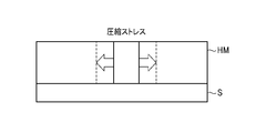
一方、上述したように、wigglingはハードマスクを構成する膜の上端でストレスが開放することにより生じる。このため、以下に説明するように、引張りストレス(膜が収縮しようとするストレス)が生じているほうがwiggling防止には有利である。 On the other hand, as described above, wigging occurs when stress is released at the upper end of the film constituting the hard mask. Therefore, as described below, it is advantageous to prevent wigging when tensile stress (stress at which the film tends to contract) is generated.
図2に示すように、エッチング後のハードマスクHMに圧縮ストレス(膜が膨張しようとするストレス)が生じている場合、ハードマスクHMを構成する膜は拡がろうとする。しかし、膜の底部は下地膜(基板)Sに拘束されて膨張は阻止され、膜の上端部分のみが拡がるため、上端部分にwigglingが生じる。これに対して、図3に示すように、エッチング後のハードマスクHMに引張りストレス(膜が収縮しようとするストレス)が生じている場合、膜は縮もうとする。しかし、ハードマスクを構成する膜の底部は下地膜(基板)Sに拘束されて収縮は阻止され、膜の上端部分では引っ張られるため、wigglingは生じ難いと考えられる。このため、ハードマスクを構成する膜に、適度な引張り応力を付与することにより、エッチングパターンがより微細化しても、wigglingの発生を抑制できると考えられる。 As shown in FIG. 2, when the hard mask HM after etching is subjected to compression stress (stress that the film tries to expand), the film constituting the hard mask HM tends to expand. However, the bottom portion of the film is constrained by the underlying film (substrate) S to prevent expansion, and only the upper end portion of the film expands, so that wiggling occurs at the upper end portion. On the other hand, as shown in FIG. 3, when the hard mask HM after etching is subjected to tensile stress (stress at which the film tends to shrink), the film tends to shrink. However, since the bottom portion of the film constituting the hard mask is restrained by the underlying film (substrate) S to prevent shrinkage and is pulled at the upper end portion of the film, it is considered that wigging is unlikely to occur. Therefore, it is considered that by applying an appropriate tensile stress to the film constituting the hard mask, the occurrence of wigging can be suppressed even if the etching pattern becomes finer.
しかし、図4Aに示すように、ハードマスク用膜Fの膜ストレスが膜内で一様な引張りストレス(T)になる理想的状態になるように制御しても、実際にはある程度のストレスのバラツキが生じてしまう。すなわち、実際のハードマスク用膜Fの膜中のストレス分布は、図4Bに示すように、一様な引張りストレス(T)ではない。具体的には、より強い引張りストレス(TT)の部分や、ストレスが存在しないニュートラル(0)の部分や、圧縮ストレス(C)の部分が存在する。この状態でハードマスク用膜Fをハードマスクとして用いて下地膜であるエッチング対象膜をエッチングする場合、ハードマスクのエッチング量はプロセスによって変化する。このため、図4Bに示すようにエッチング停止位置ESも変化し、これにともなってエッチング停止位置ESのストレスも変化する。パターンの幅が狭く、アスペクト比が大きくなると、エッチング停止位置ESのストレスによっては、wigglingが発生することがある。つまり、エッチングした後のハードマスクの上面領域のストレスが、その領域より深い領域のストレスよりも圧縮方向に向かう場合、上面領域は相対的に圧縮ストレスとなる。そのため、当該上面領域にwigglingが発生する可能性がある。 However, as shown in FIG. 4A, even if the film stress of the hard mask film F is controlled to be in an ideal state of becoming a uniform tensile stress (T) in the film, the stress is actually to some extent. There will be variations. That is, the stress distribution in the actual hard mask film F is not a uniform tensile stress (T) as shown in FIG. 4B. Specifically, there is a stronger tensile stress (TT) portion, a neutral (0) portion in which no stress exists, and a compression stress (C) portion. In this state, when the hard mask film F is used as the hard mask to etch the etching target film which is the base film, the etching amount of the hard mask changes depending on the process. Therefore, as shown in FIG. 4B, the etching stop position ES also changes, and the stress at the etching stop position ES also changes accordingly. When the width of the pattern is narrow and the aspect ratio is large, wigging may occur depending on the stress of the etching stop position ES. That is, when the stress in the upper surface region of the hard mask after etching tends toward the compression direction rather than the stress in the region deeper than that region, the upper surface region becomes relatively compressive stress. Therefore, wigging may occur in the upper surface region.
そこで、一実施形態では、ドライエッチングによりエッチングすべきエッチング対象膜の上にハードマスク用膜を成膜する際に、初期の膜ストレスが引張りストレスとなり、かつ引張りストレスが当該膜の底面から上面にかけて単調増加するように、成膜パラメータを制御しつつ成膜する。 Therefore, in one embodiment, when a film for a hard mask is formed on a film to be etched by dry etching, the initial film stress becomes tensile stress, and the tensile stress is applied from the bottom surface to the upper surface of the film. The film is formed while controlling the film forming parameters so as to increase monotonically.
このようなストレス分布を形成することにより、膜のどの部分も、それより深い部分よりも大きな引張りストレスを有する。このため、ハードマスク用膜をハードマスクとして用いてエッチング対象膜をエッチングした場合、ハードマスクのエッチングストップ位置にかかわらず、常にハードマスクの残存部分の上面側に引張り応力が作用するようになる。したがって、パターンがより微細化し、残存する部分の幅が薄く、かつその部分の形状のアスペクト比が高くなっても、wigglingの発生を有効に抑制することができる。 By forming such a stress distribution, any part of the membrane has greater tensile stress than deeper parts. Therefore, when the etching target film is etched using the hard mask film as the hard mask, the tensile stress always acts on the upper surface side of the remaining portion of the hard mask regardless of the etching stop position of the hard mask. Therefore, even if the pattern becomes finer, the width of the remaining portion is thin, and the aspect ratio of the shape of the portion is high, the occurrence of wigging can be effectively suppressed.
<ハードマスク用膜の形成方法>
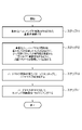
次に、一実施形態に係るハードマスク用膜の形成方法について説明する。
図5は一実施形態に係るハードマスク用膜の形成方法を示すフローチャート、図6A~6Bはその工程断面図である。
<Method of forming a hard mask film>
Next, a method for forming a hard mask film according to an embodiment will be described.
FIG. 5 is a flowchart showing a method of forming a hard mask film according to an embodiment, and FIGS. 6A to 6B are cross-sectional views of the process.
まず、基体1上にエッチング対象膜2が形成された基板3を準備する(ステップ1、図6A)。
First, a
基体1は、特に限定されないが、シリコン等の半導体が典型例として例示される。この場合は、基板3は半導体ウエハであってよい。また、エッチング対象膜2は特に限定されないが、例えば、タングステン膜、GST(GeSbTe)膜、Poly-Si膜、カーボン膜、SiO2膜、SiON膜等が例示される。また、エッチング対象膜2は、複数以上の膜が積層された積層膜であってもよい。
The
次に、基板3上に、ハードマスク用膜4を、初期の膜ストレスが引張りストレスとなり、かつ引張りストレスが当該膜の底面から上面にかけて単調増加するように、成膜パラメータを制御しつつ成膜する(ステップ2、図6B)。
Next, the
ハードマスク用膜4は、エッチング対象膜2をエッチングするためのハードマスクとして機能させるためのものであり、ハードマスクとなる膜であればよいが、SiN膜、SiO2膜、SiON膜等が好適なものとして例示される。SiN膜は、金属(Al等)を添加したものであってもよい。
The
この際の成膜方法は、特に限定されないが、CVD法を好適に用いることができる。例えば、プラズマCVD法(PE-CVD法)を用いることができる。また、プラズマCVD法で成膜する際のプラズマ源としてはマイクロ波プラズマ源を用いることができる。マイクロ波プラズマを用いることにより、比較的低温で成膜することができ、低電子温度で高密度のプラズマにより良好な膜質の膜を成膜することができる。例えば、SiN膜の場合は、250~550℃の範囲で成膜が行われ、400℃以下の低温成膜が可能である。 The film forming method at this time is not particularly limited, but the CVD method can be preferably used. For example, a plasma CVD method (PE-CVD method) can be used. Further, a microwave plasma source can be used as the plasma source when forming a film by the plasma CVD method. By using microwave plasma, a film can be formed at a relatively low temperature, and a film having a good film quality can be formed by high-density plasma at a low electron temperature. For example, in the case of a SiN film, the film is formed in the range of 250 to 550 ° C, and a low temperature film formation of 400 ° C or lower is possible.
このとき、成膜中に経時的に成膜パラメータ(プロセスパラメータ)を制御することにより、成膜するハードマスク用膜4の膜ストレスを制御することができる。例えば、マイクロ波プラズマCVDで成膜する際には、図7に示すように、成膜速度を大きくする(成膜ガス流量を多くする)ことにより、引張りストレスが大きくなる傾向となる。また、図8に示すように、圧力を高くすることにより、引張りストレスが大きくなる傾向となる。さらに、図9に示すように、プラズマ密度(パワー)を下げることにより、引張りストレスが大きくなる傾向にある。したがって、成膜パラメータとして成膜速度、圧力、プラズマ密度の少なくとも1種を制御することにより膜ストレスを制御することができる。このような成膜パラメータによる膜ストレスの制御は、他のプラズマCVDでも同様に行うことができる。
At this time, by controlling the film forming parameters (process parameters) over time during the film forming, the film stress of the
したがって、ハードマスク用膜4の成膜初期条件を膜ストレスが引張りストレスとなるような条件に設定し、上記成膜パラメータ(プロセスパラメータ)のうち少なくとも1種を、引張りストレスが単調増加するように制御する。例えば、初期の成膜条件からガス流量が漸次増加するような複数段階の処理レシピを用いて成膜を行う。
Therefore, the initial conditions for film formation of the
これにより、ハードマスク用膜を図10Aのような、ハードマスク用膜4の成膜初期の膜ストレスが引張りストレスとなり、当該膜の底面から上面にかけて引張りストレスが単調増加するストレス分布にすることができる。図10Bはこのときの膜のストレス分布を模式的に示したものである。なお、図10Bにおいて、「T」は引張りストレスを示し、「T」の数が多いほど引張りストレスが大きいことを表す。
As a result, the hard mask film can be made into a stress distribution as shown in FIG. 10A, in which the film stress at the initial stage of film formation of the
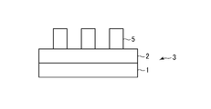
<半導体装置の製造方法>
次に、以上のように形成されたハードマスク用膜4をハードマスクとして用いた半導体装置の製造方法について説明する。
図11は一実施形態に係る半導体装置の製造方法を示すフローチャート、図12はその工程断面図である。
<Manufacturing method of semiconductor devices>
Next, a method for manufacturing a semiconductor device using the
FIG. 11 is a flowchart showing a manufacturing method of the semiconductor device according to the embodiment, and FIG. 12 is a process sectional view thereof.
まず、基体1上にエッチング対象膜2が形成された基板3を準備する(ステップ11、図12の(a))。次に、基板3上に、ハードマスク用膜4を、膜ストレスが引張りストレスとなるように、かつ引張りストレスが当該膜の底面から上面にかけて単調増加するように、成膜パラメータを制御しつつ成膜する(ステップ12、図12の(b))。これらのステップ11および12は、上記ステップ1および2と同様である。
First, a
次に、例えば、フォトリソグラフィにより所定パターンを形成し、そのパターンをマスクとして、ハードマスク用膜4を所定パターンにドライエッチングし、ハードマスク5を形成する(ステップ13、図12の(c))。
Next, for example, a predetermined pattern is formed by photolithography, and the
次に、ハードマスク5をマスクとして、エッチング対象膜2をドライエッチングする(ステップ14、図12の(d))。このエッチングにより、所定パターンでハードマスク5およびエッチング対象膜2が残存し、残存部分6となる。
Next, using the
ステップ13のハードマスク用膜4のエッチングとステップ14のエッチング対象膜2のエッチングは連続して行ってもよい。
The etching of the
半導体デバイスのスケーリング(微細化)にともない、パターン幅が薄くなっている。このため、エッチング後のエッチング対象膜2およびハードマスク5の残存部分6は、図13に示す幅Wが5~30nmと薄く、高さHは10~200nmである。幅Wが薄く高さHが高くなると、薄幅かつ高アスペクト比となるため、従来は、ハードマスク5の上面部分にwigglingが生じやすかった。
With the scaling (miniaturization) of semiconductor devices, the pattern width is becoming thinner. Therefore, the remaining
これに対し、本実施形態では、ハードマスク用膜4は、その膜ストレスが引張りストレスとなるように、かつ、引張りストレスが当該膜の底面から表面にかけて単調増加するように成膜パラメータを制御して成膜されている。すなわち、ハードマスク用膜4には、膜厚方向に引張りストレスのグラディエーションが形成される。
On the other hand, in the present embodiment, the film formation parameter of the
このようなストレス分布を形成することにより、ハードマスク用膜4のどの部分も、それより深い部分よりも大きな引張りストレスを有する。このため、ハードマスク用膜4をハードマスク5として用いてエッチング対象膜2をエッチングした場合、ハードマスク5のエッチングストップ位置にかかわらず、常にハードマスク5の上面側に引張り応力が作用するようになる。したがって、パターンがより微細化し、エッチング後の残存部分の幅が薄く、かつその部分の形状のアスペクト比が高くなっても、引張りストレスによりwigglingの発生を有効に抑制することができる。
By forming such a stress distribution, any portion of the
また、このように、ハードマスク用膜4に引張りストレスのグラディエーションが形成されることにより、ハードマスク用膜4のバルク膜ストレス自体が比較的小さくても、wigglingの抑制が可能である。このように大きなバルク膜ストレスが要求されないことにより、ハードマスク5の底面側に隣接するエッチング対象膜2に対する密着性要求条件の緩和が可能となる。
Further, by forming the gradient of tensile stress on the
さらに、ハードマスク用膜4に引張りストレスのグラディエーションが形成されることにより、インテグレーションの都合に合わせて、バルク膜ストレスを調整することが可能となる。
Further, the formation of the tensile stress gradient on the
さらにまた、wigglingを抑制するためにバルク膜ストレスを大きくする必要がないため、ハードマスク用膜4の膜質パラメータ(例えば、膜密度、モジュラス等)に対するマージンが広がる。
Furthermore, since it is not necessary to increase the bulk film stress in order to suppress wiggling, the margin for the film quality parameters (for example, film density, modulus, etc.) of the
<成膜装置>
次に、一実施形態に係るハードマスク用膜の形成に好適な成膜装置の例について説明する。本例の成膜装置は、小型のマイクロ波放射機構を複数有するマイクロ波プラズマ源を用いたマイクロ波プラズマ成膜装置として構成される。
<Film formation device>
Next, an example of a film forming apparatus suitable for forming a hard mask film according to an embodiment will be described. The film forming apparatus of this example is configured as a microwave plasma film forming apparatus using a microwave plasma source having a plurality of small microwave radiation mechanisms.
図14は、成膜装置の一例を模式的に示す断面図、図15は図14の成膜装置のマイクロ波導入装置の構成を示す構成図、図16は図14の成膜装置におけるマイクロ波放射機構を模式的に示す断面図、図17は図14の成膜装置における処理容器の天壁部を模式的に示す底面図である。 14 is a cross-sectional view schematically showing an example of the film forming apparatus, FIG. 15 is a block diagram showing the configuration of the microwave introducing apparatus of the film forming apparatus of FIG. 14, and FIG. 16 is a microwave in the film forming apparatus of FIG. A cross-sectional view schematically showing a radiation mechanism, and FIG. 17 is a bottom view schematically showing a top wall portion of a processing container in the film forming apparatus of FIG.
この成膜装置100は、処理容器101と、載置台102と、ガス供給機構103と、排気装置104と、マイクロ波導入装置105と、制御部106とを備えている。
The
処理容器101は、成膜処理に際して基板Wを収容するものであり、例えばアルミニウムおよびその合金等の金属材料によって形成され、略円筒形状をなしている。処理容器101は、板状の天壁部111および底壁部113と、これらを連結する側壁部112とを有している。
The
天壁部111には、マイクロ波導入装置105の後述するマイクロ波放射機構が嵌め込まれる複数の開口部を有している。側壁部112は、処理容器101に隣接する搬送室(図示せず)との間で成膜を行う基板Wの搬入出を行うための搬入出口114を有している。搬入出口114はゲートバルブ115により開閉されるようになっている。
The
載置台102は、処理容器101の内部で基板Wを載置するためのものであり、円板状をなしており、AlN等のセラミックスからなっている。載置台102は、処理容器101の底部中央から上方に延びる円筒状のAlN等のセラミックスからなる支持部材120により支持されている。
The mounting table 102 is for mounting the substrate W inside the
載置台102の外縁部には基板Wをガイドするためのガイドリング181が設けられている。ただし、ガイドリング181が存在しなくてもよく、また、ガイドリングが載置台102と一体となっていてもよい。また、載置台102の内部には、基板Wを昇降するための昇降ピン(図示せず)が載置台102の上面に対して突没可能に設けられている。
A
載置台102の内部には抵抗加熱型のヒータ182が埋め込まれており、このヒータ182はヒータ電源(図示せず)から給電されることにより載置台102を介してその上の基板Wを加熱する。また、載置台102には、熱電対(図示せず)が挿入されており、熱電対からの信号に基づいて、基板Wの加熱温度を、例えば200~600℃の範囲の所定の温度に制御可能となっている。
A resistance
載置台102内のヒータ182の上方には、基板Wと同程度の大きさの電極184が埋設されており、この電極184には、高周波バイアス電源122が電気的に接続されている。この高周波バイアス電源122から載置台102に、イオンを引き込むための高周波バイアスが印加される。なお、高周波バイアス電源122はプラズマ処理の特性によっては設けなくてもよい。
An
ガス供給機構103は、処理容器101内にハードマスク用膜を成膜するためのガスを処理容器内に供給するためのものである。ハードマスク用膜がSiN膜である場合、ガスとしては、Si原料ガス、例えばSiH4ガス、窒素含有ガス、例えばN2ガス、NH3ガス、プラズマ生成ガス(励起ガス)としての希ガス、例えばHeガスを用いることができる。
The
ガス供給機構103は、第1のガス供給部191と、第2のガス供給部192と、第1のガス吐出部193と、第2のガス吐出部194と、第3のガス吐出部195とを有する。
The
第1のガス供給部191からは、プラズマ生成ガスや、高エネルギーで解離させたい成膜用ガス、例えばN2ガスが、第1のガス吐出部193に供給される。第1のガス供給部191は、配管201を介して、天壁部111内に設けられた第1のガス吐出部193に接続されている。
From the first
第1のガス吐出部193は、天壁部111の内部に設けられた、天壁部111の中心を中心とした円周状をなすガス拡散空間203と、ガス拡散空間から処理容器101内に至る複数のガス吐出孔204とを有する。天壁部111の上面にはガス導入部202が設けられ、ガス導入部202には、第1のガス供給部191から延びる配管201が接続されている。したがって、第1のガス吐出部193は、第1のガス供給部191から配管201を介して供給されたプラズマ生成ガスおよび高エネルギーで解離させたいガスを、天壁部111の直下位置に吐出する。
The first
第2のガス供給部192からは、過剰解離を抑制したい成膜ガス、例えばSi原料であるSiH4ガスが、第2のガス吐出部194および第3のガス吐出部195に供給される。
From the second
第2のガス吐出部194は、天壁部111から下方に延びる複数のノズル206を有している。複数のノズル206は天壁部111の中心を中心とした円周上に等間隔で設けられている。図17ではノズル206が6個の例を示しているが、ノズル206の個数は6個に限らず、例えば、3個であっても、12個であってもよい。ノズル206内には、ガス流路207が設けられており、ガス流路207はノズル206の下端部で水平方向に屈曲し、ノズル206の側壁下部にガス吐出口(図示せず)が設けられている。各ノズル206は、配管205を介して第2のガス供給部192に接続されている。したがって、第2のガス吐出部194は、第2のガス供給部192から配管205を介して供給された過剰解離を抑制したいガスを天壁部111と載置台102の間の所定の高さ位置に吐出する。
The second
なお、第2のガス吐出部194としては、ノズル206を用いる場合に限らず、複数の天壁部111から垂下する複数(例えば6本)の柱を設け、これら柱の底部を、リング状の構造物でつなぎ、その構造物の底面に多数のガス吐出孔を設けたリングシャワーであってもよい。
The second
第3のガス吐出部195は、処理容器101の側壁部112内の天壁部111と載置台102の間の高さ位置に周方向に沿ってリング状に形成されたガス拡散空間211を有している。ガス拡散空間211は配管209を介して第2のガス供給部192に接続されている。ガス拡散空間211からは、側壁部112の内周面に至る複数のガス吐出孔212が延びており、複数のノズル213が複数のガス吐出孔212の各々に接続されている。したがって、第3のガス吐出部195は、第2のガス供給部192から配管209を介して供給された過剰解離を抑制したいガスを、外側から天壁部111と載置台102の間の所定の高さ位置に吐出する。
The third
排気装置104は底壁部113に接続された排気管116に設けられ、真空ポンプと圧力制御バルブを備えている。排気装置104の真空ポンプにより排気管116を介して処理容器101内が排気される。処理容器101内の圧力は圧力制御バルブにより制御される。
The
マイクロ波導入装置105は、処理容器101内にプラズマを生成させるためのマイクロ波を発生させるとともに、処理容器101内にマイクロ波を導入するためのものである。マイクロ波導入装置105は、処理容器101の上部に設けられ、処理容器101内に電磁波(マイクロ波)を導入してマイクロ波プラズマを生成するプラズマ生成手段として機能する。
The
マイクロ波導入装置105は、図14に示すように、処理容器101の天壁部111と、マイクロ波出力部130と、アンテナユニット140とを有する。天壁部111は天板として機能する。また、マイクロ波出力部130は、マイクロ波を生成するとともに、マイクロ波を複数の経路に分配して出力する。アンテナユニット140は、マイクロ波出力部130から出力されたマイクロ波を処理容器101に導入する。
As shown in FIG. 14, the
マイクロ波出力部130は、図15に示すように、マイクロ波電源131と、マイクロ波発振器132と、アンプ133と、分配器134とを有している。マイクロ波発振器132はソリッドステートであり、例えば、860MHzでマイクロ波を発振(例えば、PLL発振)させる。なお、マイクロ波の周波数は、860MHzに限らず、2.45GHz、8.35GHz、5.8GHz、1.98GHz等、700MHzから10GHzの範囲のものを用いることができる。アンプ133は、マイクロ波発振器132によって発振されたマイクロ波を増幅する。分配器134は、アンプ133によって増幅されたマイクロ波を複数の経路に分配するもので、入力側と出力側のインピーダンスを整合させながらマイクロ波を分配する。
As shown in FIG. 15, the
アンテナユニット140は、図15に示すように、複数のアンテナモジュール141を含んでいる。複数のアンテナモジュール141は、それぞれ、分配器134によって分配されたマイクロ波を処理容器101内に導入する。複数のアンテナモジュール141の構成は全て同一である。各アンテナモジュール141は、分配されたマイクロ波を主に増幅して出力するアンプ部142と、アンプ部142から出力されたマイクロ波を処理容器101内に放射するマイクロ波放射機構143とを有する。
As shown in FIG. 15, the
アンプ部142は、位相器145と、可変ゲインアンプ146と、メインアンプ147と、アイソレータ148とを有する。位相器145は、マイクロ波の位相を変化させる。可変ゲインアンプ146は、メインアンプ147に入力されるマイクロ波の電力レベルを調整する。メインアンプ147は、ソリッドステートアンプとして構成される。アイソレータ148は、後述するマイクロ波放射機構143のアンテナ部で反射されてメインアンプ147に向かう反射マイクロ波を分離する。
The
図14に示すように、複数のマイクロ波放射機構143は、天壁部111に設けられている。また、マイクロ波放射機構143は、図16に示すように、同軸管151と、給電部155と、チューナ154と、アンテナ部156を有する。
As shown in FIG. 14, a plurality of
同軸管151は、筒状をなす外側導体152および外側導体152内に外側導体152と同軸状に設けられた内側導体153を有し、それらの間がマイクロ波伝送路となる。
The
給電部155は、アンプ部142からの増幅されたマイクロ波をマイクロ波伝送路に給電するもので、同軸ケーブルにより、外側導体152の上端部の側方から増幅されたマイクロ波をマイクロ波伝送路に導入する。給電部155は、例えば、給電アンテナによりマイクロ波を放射することによりマイクロ波伝送路にマイクロ波電力を給電する。給電されたマイクロ波電力は、アンテナ部156に向かって伝播する。
The
アンテナ部156は、同軸管151からのマイクロ波を処理容器101内に放射するものであり、同軸管151の下端部に設けられている。アンテナ部156は、内側導体153の下端部に接続された平面アンテナ161と、平面アンテナ161の上面側に配置された遅波材162と、平面アンテナ161の下面側に配置されたマイクロ波透過板163とを有している。
The
平面アンテナ161は、円板状をなし、上下に貫通するように形成されたスロット161aを有している。スロット161aの形状は、マイクロ波が効率良く放射されるように適宜設定される。スロット161aには誘電体が挿入されていてもよい。
The
マイクロ波透過板163は天壁部111に嵌め込まれており、その下面は処理容器101の内部空間に露出している。マイクロ波透過板163は誘電体で構成されマイクロ波をTEモードで効率的に放射することができるような形状をなしている。そして、マイクロ波透過板163を透過したマイクロ波は、処理容器101内の空間にプラズマを生成する。
The
遅波材162は、真空よりも大きい誘電率を有する材料によって形成されており、その厚さによりマイクロ波の位相を調整することができ、マイクロ波の放射エネルギーが最大となるようにすることができる。
The
遅波材162およびマイクロ波透過板163を構成する材料としては、例えば、石英やセラミックス、ポリテトラフルオロエチレン樹脂等のフッ素系樹脂、ポリイミド樹脂等を用いることができる。
As the material constituting the
チューナ154は、スラグチューナを構成しており、図16に示すように、2つのスラグ171a、171bと、アクチュエータ172と、アクチュエータ172を制御するチューナコントローラ173とを有している。スラグ171a、171bは、同軸管151のアンテナ部156よりも基端部側(上端部側)の部分に配置されている。アクチュエータ172は、スラグ171a、171bをそれぞれ独立して駆動する。
The
スラグ171a,171bは、板状かつ環状をなし、セラミックス等の誘電体材料で構成され、同軸管151の外側導体152と内側導体153の間に配置されている。また、アクチュエータ172は、例えば、内側導体153の内部に設けられた、それぞれスラグ171a,171bが螺号する2本のねじを回転させることによりスラグ171a,171bを個別に駆動する。そして、チューナコントローラ173からの指令に基づいて、アクチュエータ172によって、スラグ171a,171bを上下方向に移動させる。チューナコントローラ173は、終端部のインピーダンスが50Ωになるように、スラグ171a,171bの位置を調整する。
The
メインアンプ147と、チューナ154と、平面アンテナ161とは近接配置している。そして、チューナ154と平面アンテナ161とは集中定数回路を構成し、かつ共振器として機能する。平面アンテナ161の取り付け部分には、インピーダンス不整合が存在するが、チューナ154によりプラズマ負荷に対して直接チューニングするので、プラズマを含めて高精度でチューニングすることができる。このため、平面アンテナ161における反射の影響を解消することができる。
The
図17に示すように、本例では、マイクロ波放射機構143は7本設けられており、これらに対応するマイクロ波透過板163は、均等に六方最密配置になるように配置されている。すなわち、7つのマイクロ波透過板163のうち1つは、天壁部111の中央に配置され、その周囲に、他の6つのマイクロ波透過板163が配置されている。これら7つのマイクロ波透過板163は隣接するマイクロ波透過板が等間隔になるように配置されている。また、ガス供給機構103における第2のガス吐出部194における複数(本例では6個)のノズル206は、中央のマイクロ波透過板の周囲を囲むように配置されている。第1のガス吐出部193の複数(本例では12個)のガス吐出孔204も同様に、中央のマイクロ波透過板の周囲を囲むように配置されている。なお、マイクロ波放射機構143の本数は7本に限るものではない。
As shown in FIG. 17, in this example, seven
制御部106は、典型的にはコンピュータからなり、成膜装置100の各部を制御するようになっている。制御部106は成膜装置100のプロセスシーケンスおよび制御パラメータであるプロセスレシピを記憶した記憶部や、入力手段およびディスプレイ等を備えており、選択されたプロセスレシピに従って所定の制御を行うことが可能である。
The
このように構成される成膜装置100により上記実施形態に従ってハードマスク用膜を形成するに際しては、まず、基板Wとして例えばシリコン等の半導体基体上にエッチング対象膜が形成された半導体ウエハを搬入し、載置台102の上に載置する。
When forming a hard mask film according to the above embodiment by the
次いで、処理容器101内の圧力および基板温度を所定の値に制御し、マイクロ波プラズマCVDによりハードマスク用膜を形成する。本例では、ハードマスク用膜としてSiN膜を形成する。
Next, the pressure in the
成膜に際しては、第1のガス供給部191から、プラズマ生成ガスであるHeガスを第1のガス吐出部193に供給し、複数のガス吐出孔204から処理容器101の天壁部111の直下領域に吐出する。それとともに、マイクロ波導入装置105のマイクロ波出力部130から複数に分配して出力されたマイクロ波を、アンテナユニット140の複数のアンテナモジュール141に導き、これらのマイクロ波放射機構143から放射させ、プラズマを着火させる。
At the time of film formation, He gas, which is a plasma generating gas, is supplied from the first
各アンテナモジュール141では、マイクロ波は、ソリッドステートアンプを構成するメインアンプ147で個別に増幅され、各マイクロ波放射機構143に給電され、同軸管151を伝送されてアンテナ部156に至る。その際に、マイクロ波は、チューナ154のスラグ171aおよびスラグ171bによりインピーダンスが自動整合される。このため、マイクロ波は、電力反射が実質的にない状態で、チューナ154からアンテナ部156の遅波材162を経て平面アンテナ161のスロット161aから放射される。そして、マイクロ波は、さらにマイクロ波透過板163を透過し、プラズマに接するマイクロ波透過板163の表面(下面)を伝送されて表面波を形成する。各アンテナ部156からのマイクロ波電力が処理容器101内で空間合成され、天壁部111の直下領域にHeガスによる表面波プラズマが生成される。
In each
そして、プラズマが着火したタイミングで、窒素含有ガスである例えばN2ガスまたはNH3ガスを、第1のガス供給部191から供給し、第1のガス吐出部193から吐出する。また、Si原料ガスである例えばSiH4ガスを、第2のガス供給部192から供給し、第2のガス吐出部194および第3のガス供給部195から吐出する。これにより窒素含有ガスとSi原料ガスとがプラズマにより励起されて反応し、基板W上にSiN膜が形成される。窒素含有ガスは、処理容器101の天壁部111の直下領域に吐出されるため、表面波プラズマにより十分に解離し、Si原料ガスは表面波プラズマから離れた位置に供給されて過剰解離が抑制される。
Then, at the timing when the plasma is ignited, nitrogen-containing gas such as N2 gas or NH3 gas is supplied from the first
このとき、窒化膜を、膜ストレスが、当該膜のいずれの部分も引張りストレスとなり、引張りストレスが当該膜の底面から上面にかけて単調増加するようにプロセスパラメータを制御する。このときのプロセスパラメータとしては、窒素含有ガスおよび/またはSi原料ガスの流量、圧力、マイクロ波パワー等を挙げることができる。これらのプロセスパラメータの少なくとも一種を成膜中に変化させる。例えば、窒素含有ガスおよび/またはSi原料ガスの流量が漸次増加するような複数段階の処理レシピを用いて成膜を行う。 At this time, the process parameters of the nitride film are controlled so that the film stress becomes tensile stress in any part of the film and the tensile stress increases monotonically from the bottom surface to the upper surface of the film. Examples of the process parameters at this time include the flow rate, pressure, microwave power, and the like of the nitrogen-containing gas and / or the Si raw material gas. At least one of these process parameters is changed during film formation. For example, the film formation is performed using a multi-step treatment recipe in which the flow rate of the nitrogen-containing gas and / or the Si raw material gas is gradually increased.
本例の成膜装置100では、大型のアイソレータや合成器が不要となり、コンパクトな装置構成で、反射の影響を確実に解消して高精度のプラズマ制御が可能となる。また、マイクロ波プラズマを用いることにより、成膜温度(基板温度)を400℃以下に低温化することができ、かつ低電子温度で高密度のプラズマにより良好な膜質の膜を成膜することができる。
The
<他の適用>
以上、実施形態について説明したが、今回開示された実施形態は、全ての点で例示であって制限的なものではないと考えられるべきである。上記の実施形態は、添付の特許請求の範囲およびその主旨を逸脱することなく、様々な形態で省略、置換、変更されてもよい。
<Other applications>
Although the embodiments have been described above, the embodiments disclosed this time should be considered to be exemplary in all respects and not restrictive. The above embodiments may be omitted, replaced or modified in various forms without departing from the scope of the appended claims and their gist.
例えば、上記実施形態ではハードマスク用膜の形成にマイクロ波プラズマCVD成膜装置を用いたが、これに限らず、他のプラズマCVD成膜装置であっても、プラズマを用いないCVD成膜装置であってもよい。また、CVDに限らず、ALDやPVD等、他の成膜手法であってもよい。 For example, in the above embodiment, the microwave plasma CVD film forming apparatus is used for forming the hard mask film, but the present invention is not limited to this, and other plasma CVD film forming apparatus is also a CVD film forming apparatus that does not use plasma. May be. Further, the film forming method is not limited to CVD, and other film forming methods such as ALD and PVD may be used.
また、上記実施形態では、成膜装置として枚葉式の装置を用いた例を示したが、複数の基板を一度に処理するバッチ式装置やセミバッチ式装置であってもよい。 Further, in the above embodiment, an example in which a single-wafer type device is used as the film forming device is shown, but a batch type device or a semi-batch type device that processes a plurality of substrates at once may be used.
1;基体
2;エッチング対象膜
3;基板
4;ハードマスク用膜
5;ハードマスク
6;残存部分
100;成膜装置
1;
Claims (16)
基体上にエッチング対象膜が形成された基板を準備する工程と、
前記基板上に、ハードマスク用膜を、初期の膜ストレスが引張りストレスとなり、かつ引張りストレスが当該膜の底面から上面にかけて単調増加するように、成膜パラメータを制御しつつ成膜する工程と、
を有する、方法。 It is a method of forming a hard mask film.
The process of preparing a substrate on which an etching target film is formed on the substrate, and
A step of forming a hard mask film on the substrate while controlling the film forming parameters so that the initial film stress becomes tensile stress and the tensile stress increases monotonically from the bottom surface to the upper surface of the film.
The method.
基体上にエッチング対象膜が形成された基板を準備する工程と、
前記基板上に、ハードマスク用膜を、初期の膜ストレスが引張りストレスとなり、かつ引張りストレスが当該膜の底面から上面にかけて単調増加するように、成膜パラメータを制御しつつ成膜する工程と、
前記ハードマスク用膜を所定パターンにエッチングし、ハードマスクを形成する工程と、
前記ハードマスクをマスクとして前記エッチング対象膜をエッチングする工程と、
を有する、方法。 It is a manufacturing method of semiconductor devices.
The process of preparing a substrate on which an etching target film is formed on the substrate, and
A step of forming a hard mask film on the substrate while controlling the film forming parameters so that the initial film stress becomes tensile stress and the tensile stress increases monotonically from the bottom surface to the upper surface of the film.
The process of etching the hard mask film into a predetermined pattern to form a hard mask, and
The step of etching the etching target film using the hard mask as a mask, and
The method.
基板を収容する処理容器と、
前記処理容器内で基板を載置する載置台と、
前記載置台上の被処理基板を加熱する加熱部と、
前記処理容器の天壁から前記処理容器内にマイクロ波を導入するマイクロ波導入部と、
前記処理容器内に成膜に用いる成膜ガスを供給するガス供給部と、
前記処理容器内を排気する排気部と、
制御部と、
を有し、
前記マイクロ波により成膜ガスのプラズマを生成し、該プラズマにより前記ハードマスク用膜を成膜し、
前記制御部は、ハードマスク用膜の初期の膜ストレスが引張りストレスとなり、かつ引張りストレスが当該膜の底面から上面にかけて単調増加するように、成膜パラメータを制御する、装置。 A device for forming a film for a hard mask.
A processing container for accommodating the substrate and
A mounting table on which the substrate is placed in the processing container,
A heating unit that heats the substrate to be processed on the table described above,
A microwave introduction unit that introduces microwaves into the processing container from the top wall of the processing container,
A gas supply unit that supplies a film forming gas used for film formation in the processing container,
An exhaust unit that exhausts the inside of the processing container and
Control unit and
Have,
The plasma of the film-forming gas is generated by the microwave, and the film for the hard mask is formed by the plasma.
The control unit is a device that controls film formation parameters so that the initial film stress of the hard mask film becomes tensile stress and the tensile stress increases monotonically from the bottom surface to the top surface of the film.
マイクロ波を出力するマイクロ波出力部と、
前記マイクロ波出力部からマイクロ波が給電され、インピーダンス整合を行うチューナと、給電されたマイクロ波を放射するスロットを有する平面アンテナと、前記スロットから放射されたマイクロ波を透過するマイクロ波透過板とを有する複数のマイクロ波放射機構と、
を有する、請求項13に記載の装置。 The microwave introduction unit is
A microwave output unit that outputs microwaves and
A tuner that feeds microwaves from the microwave output unit to perform impedance matching, a planar antenna that has a slot that radiates the fed microwaves, and a microwave transmission plate that transmits the microwaves radiated from the slots. With multiple microwave radiation mechanisms,
13. The apparatus of claim 13.
Priority Applications (3)
| Application Number | Priority Date | Filing Date | Title |
|---|---|---|---|
| JP2018139051A JP7045954B2 (en) | 2018-07-25 | 2018-07-25 | A method and device for forming a hard mask film, and a method for manufacturing a semiconductor device. |
| US16/510,519 US10879069B2 (en) | 2018-07-25 | 2019-07-12 | Method and apparatus for forming hard mask film and method for manufacturing semiconductor devices |
| KR1020190089311A KR102259647B1 (en) | 2018-07-25 | 2019-07-24 | Method and apparatus for forming hard mask film and method for manufacturing semiconductor devices |
Applications Claiming Priority (1)
| Application Number | Priority Date | Filing Date | Title |
|---|---|---|---|
| JP2018139051A JP7045954B2 (en) | 2018-07-25 | 2018-07-25 | A method and device for forming a hard mask film, and a method for manufacturing a semiconductor device. |
Publications (2)
| Publication Number | Publication Date |
|---|---|
| JP2020017606A JP2020017606A (en) | 2020-01-30 |
| JP7045954B2 true JP7045954B2 (en) | 2022-04-01 |
Family
ID=69178595
Family Applications (1)
| Application Number | Title | Priority Date | Filing Date |
|---|---|---|---|
| JP2018139051A Active JP7045954B2 (en) | 2018-07-25 | 2018-07-25 | A method and device for forming a hard mask film, and a method for manufacturing a semiconductor device. |
Country Status (3)
| Country | Link |
|---|---|
| US (1) | US10879069B2 (en) |
| JP (1) | JP7045954B2 (en) |
| KR (1) | KR102259647B1 (en) |
Families Citing this family (1)
| Publication number | Priority date | Publication date | Assignee | Title |
|---|---|---|---|---|
| US11574808B2 (en) | 2021-02-16 | 2023-02-07 | Tokyo Electron Limited | Plasma processing method and plasma processing apparatus |
Citations (3)
| Publication number | Priority date | Publication date | Assignee | Title |
|---|---|---|---|---|
| US20080054415A1 (en) | 2006-08-31 | 2008-03-06 | Kai Frohberg | n-channel field effect transistor having a contact etch stop layer in combination with an interlayer dielectric sub-layer having the same type of intrinsic stress |
| JP2009246129A (en) | 2008-03-31 | 2009-10-22 | Tokyo Electron Ltd | Method for forming plasma cvd silicon nitride film and method for manufacturing semiconductor integrated circuit device |
| JP2013543281A (en) | 2010-11-22 | 2013-11-28 | アプライド マテリアルズ インコーポレイテッド | Composite removable hard mask |
Family Cites Families (8)
| Publication number | Priority date | Publication date | Assignee | Title |
|---|---|---|---|---|
| JP2993675B2 (en) * | 1989-02-08 | 1999-12-20 | 株式会社日立製作所 | Plasma processing method and apparatus |
| KR100557581B1 (en) * | 2003-11-28 | 2006-03-03 | 주식회사 하이닉스반도체 | Manufacturing method for semicondutor device |
| US7834399B2 (en) * | 2007-06-05 | 2010-11-16 | International Business Machines Corporation | Dual stress memorization technique for CMOS application |
| JP2009246131A (en) | 2008-03-31 | 2009-10-22 | Tokyo Electron Ltd | Method of forming high-stress thin film, and method of manufacturing semiconductor integrated circuit device |
| JP2012015343A (en) | 2010-07-01 | 2012-01-19 | Hitachi High-Technologies Corp | Plasma etching method |
| US9117668B2 (en) * | 2012-05-23 | 2015-08-25 | Novellus Systems, Inc. | PECVD deposition of smooth silicon films |
| JP6356029B2 (en) | 2014-09-25 | 2018-07-11 | 東京エレクトロン株式会社 | Metal hard mask and manufacturing method thereof |
| JP6363266B2 (en) | 2017-06-22 | 2018-07-25 | 株式会社日立ハイテクノロジーズ | Manufacturing method of semiconductor device |
-
2018
- 2018-07-25 JP JP2018139051A patent/JP7045954B2/en active Active
-
2019
- 2019-07-12 US US16/510,519 patent/US10879069B2/en active Active
- 2019-07-24 KR KR1020190089311A patent/KR102259647B1/en active IP Right Grant
Patent Citations (3)
| Publication number | Priority date | Publication date | Assignee | Title |
|---|---|---|---|---|
| US20080054415A1 (en) | 2006-08-31 | 2008-03-06 | Kai Frohberg | n-channel field effect transistor having a contact etch stop layer in combination with an interlayer dielectric sub-layer having the same type of intrinsic stress |
| JP2009246129A (en) | 2008-03-31 | 2009-10-22 | Tokyo Electron Ltd | Method for forming plasma cvd silicon nitride film and method for manufacturing semiconductor integrated circuit device |
| JP2013543281A (en) | 2010-11-22 | 2013-11-28 | アプライド マテリアルズ インコーポレイテッド | Composite removable hard mask |
Also Published As
| Publication number | Publication date |
|---|---|
| US10879069B2 (en) | 2020-12-29 |
| JP2020017606A (en) | 2020-01-30 |
| KR102259647B1 (en) | 2021-06-03 |
| KR20200011888A (en) | 2020-02-04 |
| US20200035491A1 (en) | 2020-01-30 |
Similar Documents
| Publication | Publication Date | Title |
|---|---|---|
| JP6960813B2 (en) | Graphene structure forming method and forming device | |
| US20210164103A1 (en) | Film forming method and processing apparatus | |
| JP6752117B2 (en) | Microwave plasma source and microwave plasma processing equipment | |
| JP6700118B2 (en) | Plasma deposition apparatus and substrate mounting table | |
| KR20070108929A (en) | Microwave plasma processing device | |
| US20190237326A1 (en) | Selective film forming method and film forming apparatus | |
| KR101681061B1 (en) | Plasma treatment method and plasma treatment device | |
| JP7045954B2 (en) | A method and device for forming a hard mask film, and a method for manufacturing a semiconductor device. | |
| WO2021131480A1 (en) | Film formation method and film formation apparatus | |
| WO2021220841A1 (en) | Pre-coating method and treatment device | |
| WO2021205928A1 (en) | Cleaning method and plasma treatment device | |
| US10190217B2 (en) | Plasma film-forming method and plasma film-forming apparatus | |
| US11145522B2 (en) | Method of forming boron-based film, and film forming apparatus | |
| US20220316065A1 (en) | Processing apparatus and film forming method | |
| WO2022102463A1 (en) | Substrate treatment method and substrate treatment device | |
| JP2019102508A (en) | Method and apparatus for forming boron-based film | |
| WO2021246023A1 (en) | Plasma processing device and plasma processing method | |
| JP2024004544A (en) | Substrate treatment method and substrate treatment apparatus |
Legal Events
| Date | Code | Title | Description |
|---|---|---|---|
| A621 | Written request for application examination |
Free format text: JAPANESE INTERMEDIATE CODE: A621 Effective date: 20210426 |
|
| TRDD | Decision of grant or rejection written | ||
| A977 | Report on retrieval |
Free format text: JAPANESE INTERMEDIATE CODE: A971007 Effective date: 20220217 |
|
| A01 | Written decision to grant a patent or to grant a registration (utility model) |
Free format text: JAPANESE INTERMEDIATE CODE: A01 Effective date: 20220222 |
|
| A61 | First payment of annual fees (during grant procedure) |
Free format text: JAPANESE INTERMEDIATE CODE: A61 Effective date: 20220322 |
|
| R150 | Certificate of patent or registration of utility model |
Ref document number: 7045954 Country of ref document: JP Free format text: JAPANESE INTERMEDIATE CODE: R150 |