JP7026140B2 - Measurement of height difference in pattern on semiconductor wafer - Google Patents
Measurement of height difference in pattern on semiconductor wafer Download PDFInfo
- Publication number
- JP7026140B2 JP7026140B2 JP2019563887A JP2019563887A JP7026140B2 JP 7026140 B2 JP7026140 B2 JP 7026140B2 JP 2019563887 A JP2019563887 A JP 2019563887A JP 2019563887 A JP2019563887 A JP 2019563887A JP 7026140 B2 JP7026140 B2 JP 7026140B2
- Authority
- JP
- Japan
- Prior art keywords
- trench
- height difference
- core
- gap
- physical parameters
- Prior art date
- Legal status (The legal status is an assumption and is not a legal conclusion. Google has not performed a legal analysis and makes no representation as to the accuracy of the status listed.)
- Active
Links
Images


Classifications
-
- H—ELECTRICITY
- H01—ELECTRIC ELEMENTS
- H01L—SEMICONDUCTOR DEVICES NOT COVERED BY CLASS H10
- H01L22/00—Testing or measuring during manufacture or treatment; Reliability measurements, i.e. testing of parts without further processing to modify the parts as such; Structural arrangements therefor
- H01L22/10—Measuring as part of the manufacturing process
- H01L22/12—Measuring as part of the manufacturing process for structural parameters, e.g. thickness, line width, refractive index, temperature, warp, bond strength, defects, optical inspection, electrical measurement of structural dimensions, metallurgic measurement of diffusions
-
- G—PHYSICS
- G06—COMPUTING; CALCULATING OR COUNTING
- G06T—IMAGE DATA PROCESSING OR GENERATION, IN GENERAL
- G06T7/00—Image analysis
- G06T7/0002—Inspection of images, e.g. flaw detection
- G06T7/0004—Industrial image inspection
- G06T7/0006—Industrial image inspection using a design-rule based approach
-
- G—PHYSICS
- G01—MEASURING; TESTING
- G01B—MEASURING LENGTH, THICKNESS OR SIMILAR LINEAR DIMENSIONS; MEASURING ANGLES; MEASURING AREAS; MEASURING IRREGULARITIES OF SURFACES OR CONTOURS
- G01B15/00—Measuring arrangements characterised by the use of electromagnetic waves or particle radiation, e.g. by the use of microwaves, X-rays, gamma rays or electrons
- G01B15/02—Measuring arrangements characterised by the use of electromagnetic waves or particle radiation, e.g. by the use of microwaves, X-rays, gamma rays or electrons for measuring thickness
- G01B15/025—Measuring arrangements characterised by the use of electromagnetic waves or particle radiation, e.g. by the use of microwaves, X-rays, gamma rays or electrons for measuring thickness by measuring absorption
-
- G—PHYSICS
- G01—MEASURING; TESTING
- G01Q—SCANNING-PROBE TECHNIQUES OR APPARATUS; APPLICATIONS OF SCANNING-PROBE TECHNIQUES, e.g. SCANNING PROBE MICROSCOPY [SPM]
- G01Q90/00—Scanning-probe techniques or apparatus not otherwise provided for
-
- G—PHYSICS
- G06—COMPUTING; CALCULATING OR COUNTING
- G06T—IMAGE DATA PROCESSING OR GENERATION, IN GENERAL
- G06T7/00—Image analysis
- G06T7/0002—Inspection of images, e.g. flaw detection
- G06T7/0004—Industrial image inspection
-
- G—PHYSICS
- G06—COMPUTING; CALCULATING OR COUNTING
- G06T—IMAGE DATA PROCESSING OR GENERATION, IN GENERAL
- G06T7/00—Image analysis
- G06T7/60—Analysis of geometric attributes
-
- H—ELECTRICITY
- H01—ELECTRIC ELEMENTS
- H01L—SEMICONDUCTOR DEVICES NOT COVERED BY CLASS H10
- H01L22/00—Testing or measuring during manufacture or treatment; Reliability measurements, i.e. testing of parts without further processing to modify the parts as such; Structural arrangements therefor
- H01L22/20—Sequence of activities consisting of a plurality of measurements, corrections, marking or sorting steps
-
- H—ELECTRICITY
- H01—ELECTRIC ELEMENTS
- H01L—SEMICONDUCTOR DEVICES NOT COVERED BY CLASS H10
- H01L22/00—Testing or measuring during manufacture or treatment; Reliability measurements, i.e. testing of parts without further processing to modify the parts as such; Structural arrangements therefor
- H01L22/30—Structural arrangements specially adapted for testing or measuring during manufacture or treatment, or specially adapted for reliability measurements
-
- G—PHYSICS
- G06—COMPUTING; CALCULATING OR COUNTING
- G06T—IMAGE DATA PROCESSING OR GENERATION, IN GENERAL
- G06T2207/00—Indexing scheme for image analysis or image enhancement
- G06T2207/30—Subject of image; Context of image processing
- G06T2207/30108—Industrial image inspection
- G06T2207/30148—Semiconductor; IC; Wafer
Description
本開示は、一般に、半導体ウエハ上のパターンの寸法の測定に関し、詳細には、パターン内の高低差および/または幅差の測定に関する。 The present disclosure relates generally to measuring the dimensions of a pattern on a semiconductor wafer, and more specifically to measuring height and / or width differences within a pattern.
半導体ウエハの検査など、様々なマッピングおよび撮像の適用分野において、走査電子顕微鏡(SEM)画像が使用されている。SEM画像を使用するウエハの3次元(3D)マッピングのために、いくつかの技法が当技術分野では知られている。たとえば、半導体デバイスを検査する従来の技法では、SEMによって取得された複数組の測定データを利用して、半導体デバイスの寸法パラメータを判定する。SEMは、デバイスに対して異なる角度配向から各組のデータを収集する。半導体デバイスの寸法パラメータは、SEM検査角度と収集したデータセットとの関係を分析することによって判定される。 Scanning electron microscope (SEM) images are used in various mapping and imaging applications, such as inspection of semiconductor wafers. Several techniques are known in the art for three-dimensional (3D) mapping of wafers using SEM images. For example, in the conventional technique of inspecting a semiconductor device, a plurality of sets of measurement data acquired by SEM are used to determine dimensional parameters of the semiconductor device. The SEM collects each set of data from different angular orientations with respect to the device. The dimensional parameters of the semiconductor device are determined by analyzing the relationship between the SEM inspection angle and the collected data set.
以下は、本開示のいくつかの態様の基本的な理解を提供するための本開示の簡略化された概要である。この概要は、本開示の総括ではない。この概要は、本開示の主要または重要な要素を特定することも、本開示のいかなる特定の実装の範囲または特許請求の範囲のいかなる範囲を定めることも意図していない。この概要の唯一の目的は、後に提示するより詳細な説明に対する導入として、本開示のいくつかの概念を簡略化された形で提示することである。 The following is a simplified overview of the disclosure to provide a basic understanding of some aspects of the disclosure. This summary is not a summary of this disclosure. This summary is not intended to identify the main or important elements of this disclosure or to define any particular scope of implementation or claims of this disclosure. The sole purpose of this overview is to present some of the concepts of the present disclosure in a simplified form as an introduction to the more detailed description presented later.
実際の測定値(たとえば、SEM画像からの測定値)および高低差判定モデルを使用することによって、半導体ウエハ上に設けられたパターン内の高低差を判定するための改善された技法が、本明細書に開示される。この適用分野では、「パターン」という用語が、半導体ウエハ上に形成されるあらゆる3D構造を包含する。 An improved technique for determining height differences within a pattern provided on a semiconductor wafer by using actual measurements (eg, measurements from SEM images) and height difference determination models is described herein. Disclosure in the book. In this application, the term "pattern" includes any 3D structure formed on a semiconductor wafer.
モデルの1つのバージョンでは、モデルの測定可能な変数が、影の深さ(すなわち、相対輝度)の変化の関数の点から表現され、影の深さは、2つの特徴間の高低差ならびに幅差に依存する。 In one version of the model, the measurable variables of the model are represented in terms of a function of change in shadow depth (ie, relative brightness), where shadow depth is the height difference and width between the two features. Depends on the difference.
モデルの別のバージョンでは、測定可能な変数は、走査電子ビームの傾斜角度の変化に対する周期的な構造の実際の画像上の2つの特性点間の測定距離の変化の関数の点から表現される。 In another version of the model, the measurable variables are represented in terms of a function of the change in measurement distance between two characteristic points on the actual image of the periodic structure with respect to changes in the tilt angle of the scanning electron beam. ..
モデルの両方のバージョンでは、高低差は、実際の測定データをモデルに与えることによって、モデルから計算される。 In both versions of the model, the height difference is calculated from the model by giving the model actual measurement data.
いくつかの実装では、システムが、コンピュータプロセッサを使用して、モデルの一方または両方のバージョンを使用して高低差を抽出することが可能なモジュールを含む。システムは、ウエハを走査するSEMと、1つまたは複数のSEM画像を作成する検出器とを含むことができる。 In some implementations, the system includes a module that can use a computer processor to extract elevation differences using one or both versions of the model. The system can include an SEM that scans the wafer and a detector that produces one or more SEM images.
いくつかの実装では、非一過性コンピュータ可読媒体が、処理デバイスによって実行されると処理デバイスに方法を実施させる命令を含むことができ、この方法は、1つまたは複数のパラメータを有するコアトレンチとギャップトレンチとの間の高低差の関数として表現された変数を有するモデルを識別し、周期的な構造の実際の画像上の測定を実施して、高低差の関数の1つまたは複数のパラメータの値を取得し、コンピュータプロセッサによって、モデルを使用する高低差、および取得した1つまたは複数のパラメータを判定する。 In some implementations, a non-transient computer readable medium can include instructions that cause the processing device to perform a method when executed by the processing device, which method is a core trench with one or more parameters. Identify a model with variables expressed as a function of height difference between and a gap trench, perform actual image measurements of the periodic structure, and one or more parameters of the function of height difference. The value of is obtained, and the computer processor determines the height difference using the model and one or more of the obtained parameters.
本開示は、後述する詳細な説明および本開示の様々な実装の添付の図面から、より完全に理解される。 The present disclosure is more fully understood from the detailed description below and the accompanying drawings of the various implementations of the present disclosure.
本開示の態様は、同じ半導体ウエハ上の2つの特徴間の高低差ならびに/もしくは高低差および幅差の両方、またはプロセス変動による2つの異なる半導体ウエハ上の同じパターン特徴間の高さおよび/もしくは幅の変動を判定することを対象とする。 Aspects of the present disclosure are height differences and / or both height differences and width differences between two features on the same semiconductor wafer, or heights and / or heights between the same pattern features on two different semiconductor wafers due to process variation. The purpose is to determine the variation in width.
半導体ウエハ上に形成されるパターンは通常、様々な形状および寸法を有する特徴/オブジェクトを含む。パターンは、周期的な構造または不規則な構造を含むことができる。そのようなオブジェクト間の高低差(ならびに/または高低差および幅差の両方)の推定は、多くの目的で、たとえば半導体ウエハの製造中に、および/または半導体ウエハの製造後に半導体ウエハの検査のために必要とされることが多い。 Patterns formed on semiconductor wafers typically include features / objects with various shapes and dimensions. The pattern can include periodic or irregular structures. Estimating height differences (and / or both height differences and width differences) between such objects is used for many purposes, such as during and / or after manufacturing semiconductor wafers for inspection of semiconductor wafers. Often needed for
既存の技法では、高低差は、個々の特徴の絶対的な高さを別個に測定し、2つの測定値を比較することによって計算される。本開示では、2つの特徴の各々のそれぞれの絶対的な高さを個々に測定する必要なく、2つの特徴間の高低差を測定するための新規でより効果的な方法について説明する。 In existing techniques, the height difference is calculated by separately measuring the absolute height of each feature and comparing the two measurements. The present disclosure describes a novel and more effective method for measuring the height difference between two features without the need to individually measure the absolute height of each of the two features.
本開示における手法の利点は、2つの特徴間に相対的な高低差がある限り、2つの特徴が互いに物理的に隣接していても隣接していなくてもよいことである。加えて、2つの特徴間の幅差は、追加のプロセス制御パラメータとして判定することができる。2つの特徴は、同じパターンの一部であっても、異なるパターンの一部であってもよい。また、2つの特徴は、2つの異なるウエハ上の同じ特徴であってもよい。「同じ特徴」という用語は、広く同じタイプの特徴を意味し、たとえば特徴を製作するために使用される設計意図ファイルによって定義され、または測定データ(たとえば、SEM画像からのデータ)上で実質上同様に見える。「同じ特徴」という用語は、単一のウエハまたは異なるウエハ上に製作された同じタイプの特徴に関することができる。 The advantage of the method in the present disclosure is that the two features may or may not be physically adjacent to each other as long as there is a relative height difference between the two features. In addition, the width difference between the two features can be determined as an additional process control parameter. The two features may be part of the same pattern or part of different patterns. Also, the two features may be the same feature on two different wafers. The term "same feature" broadly refers to the same type of feature, defined by, for example, a design intent file used to make the feature, or virtually on measurement data (eg, data from an SEM image). Looks the same. The term "same feature" can refer to the same type of feature made on a single wafer or different wafers.
高低差が関心の対象となり得るパターンの一例は、半導体ウエハ上に形成された周期的な構造において隣接するトレンチ間に現れ得る材料凹部またはコア-ギャップ凹部である。材料凹部は、周期的な構造における隣接するトレンチ(すなわち、コアトレンチおよびギャップトレンチ)の深さ/高さ間の平均化された差であると理解することができる。材料凹部は、半導体の製造に使用される複数パターニング(2重パターニングなど)のプロセスの結果として生じることがある。 An example of a pattern in which height differences can be of interest are material recesses or core-gap recesses that can appear between adjacent trenches in a periodic structure formed on a semiconductor wafer. Material recesses can be understood as the averaged difference between the depths / heights of adjacent trenches (ie, core trenches and gap trenches) in a periodic structure. Material recesses can occur as a result of multiple patterning (such as double patterning) processes used in the manufacture of semiconductors.
トレンチのいくつかは、側壁を有するチャネルの形で生じることがあり、チャネルは、閉じた等高線を有することも開いた等高線を有することもある。高低差(Δh)を判定することは、任意の1対のチャネル(たとえば、パターンの特有のコア-ギャップペア)に対するΔhの絶対値を判定すること、および/または周期的なパターン内の関心領域における類似のチャネルに対して存在するΔhの平均値を判定することであると理解することができる。 Some of the trenches can occur in the form of channels with side walls, which can have closed contours or open contours. Determining the height difference (Δh) is determining the absolute value of Δh for any pair of channels (eg, the pattern's unique core-gap pair) and / or the region of interest within the periodic pattern. It can be understood that it is to determine the mean value of Δh existing for a similar channel in.
開示する技法はまた、プロセスに誘起された変動による同じウエハの異なる部分上または2つの異なるウエハ上の同じ特徴内の寸法差を評価するために使用することができる。半導体デバイスの生産では、変動に対する生産プロセスの精度、再現性、および安定性が非常に重要である。プロセス制御技法は、たとえば様々な生産段階においてパターンの高さおよび幅を測定することによって、プロセスの不正確性および不安定性を制御するために実施される。 The disclosed techniques can also be used to assess dimensional differences within the same features on different parts of the same wafer or on two different wafers due to process-induced variability. In the production of semiconductor devices, the accuracy, reproducibility, and stability of the production process against fluctuations are very important. Process control techniques are practiced to control process inaccuracies and instability, for example by measuring the height and width of patterns at various production stages.
特定のシナリオでは、プロセス制御測定、特にインラインSEMプロセス制御測定により、シャドウイング情報を分析することに基づいて、基準からの高さおよび幅のようなパターン測定値の偏差に関する情報を提供することができる。 In certain scenarios, process control measurements, especially in-line SEM process control measurements, may provide information about deviations in pattern measurements such as height and width from a reference based on analyzing shadowing information. can.
図1Aは、本発明のサブシステムS1およびS2を備える例示的なシステムS3を示す。サブシステムS1は、提案される本発明の高低差判定モジュール(HDDM)を含み、HDDMは、1つまたは複数のモデリングプロセッサSP1(およびSP2、2つ以上のプロセッサが使用される場合)を含む。HDDMは、コンピュータC内に位置し、本出願に記載するモデルの2つのバージョンのうちの少なくとも1つを使用することによって、半導体パターンの特徴間の高低差Δhを判定するように構成される。S1は、コンピュータメモリMに結合される。 FIG. 1A shows an exemplary system S3 comprising subsystems S1 and S2 of the present invention. The subsystem S1 includes the proposed height difference determination module (HDDM) of the present invention, and the HDDM includes one or more modeling processors SP1 (and SP2, when two or more processors are used). The HDDM is located within the computer C and is configured to determine the height difference Δh between the features of the semiconductor pattern by using at least one of the two versions of the model described in this application. S1 is coupled to the computer memory M.
コンピュータCは、通信線Lを介してSEMからデータを受け取ることができる。SEMは、半導体ウエハW上に製造されたパターンのSEM画像を作成する。SEMまたは任意の別個の測定モジュールが、SEM画像を使用して測定を実施するように適合されている場合、測定結果はサブシステムS1へ伝送される。サブシステムS1は、制御プロセッサPによって制御することができ、制御プロセッサPは、ユーザからの命令を取得することができる。 The computer C can receive data from the SEM via the communication line L. The SEM creates an SEM image of the pattern manufactured on the semiconductor wafer W. If the SEM or any separate measurement module is adapted to perform the measurement using SEM images, the measurement results are transmitted to the subsystem S1. The subsystem S1 can be controlled by the control processor P, which can acquire an instruction from the user.
第2のサブシステムS2は、HDDM(モデリングプロセッサSP1および/またはSP2を含む)と、測定モジュールMMと、制御プロセッサPとを含む。 The second subsystem S2 includes an HDDM (including modeling processors SP1 and / or SP2), a measurement module MM, and a control processor P.
測定モジュールMMは、SEMから画像を受け取り、輝度、パターンの様々な長さ/幅の正確な測定を実施し、これらの測定値を部分的に処理することができ、プロセッサPによって制御可能とすることができる。 The measurement module MM receives an image from the SEM, makes accurate measurements of various lengths / widths of luminance and pattern, can partially process these measurements, and is controllable by the processor P. be able to.
サブシステムS1およびS2は、ディスプレイDおよびキーボードKを備えた自立型のコンピュータC内に配置することができ、コンピュータは、通信線Lを介して直接または間接的にSEMに接続される。 The subsystems S1 and S2 can be arranged in a self-supporting computer C equipped with a display D and a keyboard K, and the computer is directly or indirectly connected to the SEM via the communication line L.
拡張されたシステムS3は、電子ビームのソースおよび1つまたは複数の検出器を組み込むSEMをさらに含むことができ、検出器は、SEM内に挿入された半導体ウエハWを監視して輝度データ(すなわち、SEM画像のグレーレベルを表すデータ)を収集するように位置決めされる。SEMは、複数の検出器から収集されたデータを処理して複合SEM画像にすることができ、または収集されたデータをモジュールMMへ供給して、モジュールMM内で複合画像を形成し、測定を実施し、それらの測定値を部分的に処理することができる。 The extended system S3 can further include an SEM that incorporates the source of the electron beam and one or more detectors, which monitors the semiconductor wafer W inserted in the SEM for brightness data (ie, ie). , Data representing the gray level of the SEM image) is positioned to collect. The SEM can process the data collected from multiple detectors into a composite SEM image, or supply the collected data to the module MM to form a composite image within the module MM for measurement. It can be carried out and those measurements can be partially processed.
図1Bは、図1Aに基づくブロック図を示し、ブロックおよびモジュールへの機能および制御入力が示されている。機能入力/接続は太い矢印で示されており、制御入力/接続は細い矢印で示されている。制御プロセッサPは、MMおよびHDDM(S1の一部である)の両方を制御することに留意されたい。このブロック図では、測定モジュールMMは、S2として破線の等高線によって表示された本発明の実施形態の一部として示されている。システムS2は、Lを介してSEMに接続されたコンピュータ内に設置可能である。メモリMおよびその接続はここに図示されていない。 FIG. 1B shows a block diagram based on FIG. 1A, showing features and control inputs to blocks and modules. Function inputs / connections are indicated by thick arrows and control inputs / connections are indicated by thin arrows. Note that the control processor P controls both the MM and the HDDM (which is part of S1). In this block diagram, the measurement module MM is shown as part of an embodiment of the invention represented by dashed contour lines as S2. The system S2 can be installed in a computer connected to the SEM via L. Memory M and its connections are not shown here.
図1Cは、図2B~図7に関してより詳細に説明するように、HDDMがコア-ギャップ凹部シナリオでΔhを計算することができることを示す。これは、典型的に複数パターニングに関連する問題である。 FIG. 1C shows that the HDDM can calculate Δh in the core-gap recess scenario, as will be described in more detail with respect to FIGS. 2B-7. This is typically a problem associated with multiple patterning.
図1D(a)および図1D(b)は、複数パターニングによる材料凹部がない場合でも、プロセス変動により、2つの異なるウエハ上の同じ特徴またはウエハの異なる部分に製作された同じ特徴間に、高低差(すなわち、図1D(a)のh1と図1D(b)のh2との間の差)が生じることがあることを示す。また、プロセス変動により、幅差(すなわち、図1D(a)のw1と図1D(b)のw2との間の差)が生じることもある。第2のウエハは、同じ生産工具によって製作された同じ設計の別のウエハとすることができる。第2のウエハは、同じタイプの別の生産工具によって製作された同じ設計の別のウエハとすることもできる。第1のウエハと第2のウエハとの間の高さおよび/または幅の差は、プロセス変動、工具の不具合などに起因することがある。 1D (a) and 1D (b) show high and low between the same features on two different wafers or the same features made on different parts of the wafer due to process variation, even in the absence of material recesses due to multiple patterning. It is shown that a difference (ie, the difference between h1 in FIG. 1D (a) and h2 in FIG. 1D (b)) may occur. Further, the process variation may cause a width difference (that is, a difference between w1 in FIG. 1D (a) and w2 in FIG. 1D (b)). The second wafer can be another wafer of the same design made with the same means of production. The second wafer can also be another wafer of the same design made by another production tool of the same type. Differences in height and / or width between the first wafer and the second wafer may be due to process variations, tool defects, and the like.
図2Aは、システムS2の動作(図1Bの破線の長方形内に示す)を含むシステムS3内の動作の概略流れ図を示す。システムS2の動作は、システムS1としてのHDDMの動作を含む。測定モジュールMMは、プロセッサの制御下で1組および/または2組の測定を実施して測定結果をさらに処理する2つの実施形態のうちの少なくとも1つを含むことができる。この処理は、MMで開始し、HDDMで終了することができる。しかし、この処理は、完全にHDDMで実施することができ、したがって実際にはMMは、HDDMの一部を形成することができる。たとえば、MMは、以下に詳述するように、モデルのどのバージョンが選択されるか、またはモデルの両方のバージョンが選択されるかどうかに応じて、SEM画像上のチャネル/トレンチのグレーレベル(輝度)を測定および処理するハードウェアおよび/またはソフトウェアブロック、ならびにa)チャネルの幅「w」および/またはb)チャネル間の距離ΔXを測定および処理するハードウェアおよび/またはソフトウェアブロックを含むことができる。モデルは、ユーザによって選択することができ、またはプロセッサによって選択することができる。 FIG. 2A shows a schematic flow chart of operations within system S3, including operations of system S2 (shown within the dashed rectangle of FIG. 1B). The operation of the system S2 includes the operation of the HDDM as the system S1. The measurement module MM can include at least one of two embodiments in which one set and / or two sets of measurements are performed and the measurement results are further processed under the control of the processor. This process can start at MM and end at HDDM. However, this process can be performed entirely on the HDDM, so in practice the MM can form part of the HDDM. For example, the MM has a gray level of channels / trenches on the SEM image, depending on which version of the model is selected or both versions of the model are selected, as detailed below. May include hardware and / or software blocks that measure and process brightness), and a) channel widths "w" and / or b) hardware and / or software blocks that measure and process distance ΔX between channels. can. The model can be selected by the user or by the processor.
特定の高さのパターンのSEM画像は、パターンの高さを示す影を示し、したがって高さに依存する。電子検出器に関して、影になっている箇所から出た電子は、パターンによって吸収することができ、電子検出器に到達しない。その結果、影になっている箇所に関連する電子信号の損失は、パターンの形状寸法ならびに形状、高さおよび幅を示す。 An SEM image of a pattern of a particular height shows a shadow indicating the height of the pattern and is therefore height dependent. With respect to the electron detector, the electrons emitted from the shaded area can be absorbed by the pattern and do not reach the electron detector. As a result, the loss of the electronic signal associated with the shaded area indicates the shape dimension as well as the shape, height and width of the pattern.
本開示の一実施形態によれば、パターンのSEM画像は、そのパターンに関連する高さ依存のシャドウイングを反映するモデルを適用することによって処理され、それによって基準と比較して、SEM画像内のパターンの高さおよび/または幅の差を判定する。 According to one embodiment of the present disclosure, an SEM image of a pattern is processed by applying a model that reflects the height-dependent shadowing associated with the pattern, thereby comparing within the SEM image to a reference. Determine the difference in height and / or width of the pattern.
図1Cに示すコア-ギャップの例では、コアトレンチのSEM画像が、ギャップトレンチのSEM画像に対する基準として働くことができる。図1D(a)および図1D(b)に示す例では、第1のウエハのパターンSEM画像は、第2のウエハのパターンSEM画像に対する基準として働くことができる。どちらの例でも、高低差に関する情報が判定される。図1D(a)~図1D(b)に示すパターンは、複数パターニングに限定されるものではないことに留意されたい。 In the core-gap example shown in FIG. 1C, the SEM image of the core trench can serve as a reference to the SEM image of the gap trench. In the examples shown in FIGS. 1D (a) and 1D (b), the pattern SEM image of the first wafer can serve as a reference for the pattern SEM image of the second wafer. In both examples, information about the height difference is determined. It should be noted that the patterns shown in FIGS. 1D (a) to 1D (b) are not limited to a plurality of patterning.
本開示の一実施形態によれば、基準は、絶対寸法値、たとえば図1D(a)の高さh1または幅w1に関連付けることができる。絶対高さ値は、たとえばSEMレシピ設定ステップなどの予備のプロセス制御ステップ、またはOCD(光CD測定)もしくはTEM(透過電子顕微鏡法)などの非インライン測定技法を用いる相補的な測定ステップ中に取得することができる。基準に関連付けられた絶対高さ値、および判定された高低差を使用することによって、パターンの絶対高さ値を取得することができる。 According to one embodiment of the present disclosure, the reference can be associated with an absolute dimensional value, eg, height h1 or width w1 in FIG. 1D (a). Absolute height values are obtained during preliminary process control steps, such as the SEM recipe setting step, or complementary measurement steps using non-inline measurement techniques such as OCD (optical CD measurement) or TEM (transmission electron microscopy). can do. The absolute height value of the pattern can be obtained by using the absolute height value associated with the criterion and the determined height difference.
上述したように、高さ判定は、高低差Δhの関数として表現される変数V、すなわちV=f(Δh)を有するモデルを識別することを伴う。Vは、測定可能な値を有し、1つまたは複数の実際のパラメータの関数であり、これらの実際のパラメータのうちのいくつかは、測定することが可能である。モデルの1つのバージョンでは、変数Vは、影の深さの関数として表現され、影の深さは、隣接する特徴間の高低差ならびに幅差に依存する。モデルの別のバージョンでは、変数は、SEM画像を取得するために使用された電子ビームの傾斜角度の変化に対するSEM画像上の2つの特性点間の測定距離の変化の点から表現される。ユーザは、モデルのいずれかのバージョンを選択して高低差を判定することができる。また、モデルの複数のバージョンを使用して高低差を判定し、よりよい精度のためにそれらの結果を比較することも可能である。図2Aに示す流れ図のブロック10~15は、モデルの選択されたバージョンに応じて動作することが、当業者には容易に理解されよう。 As mentioned above, the height determination involves identifying a model having the variable V, i.e. V = f (Δh), expressed as a function of the height difference Δh. V has a measurable value and is a function of one or more actual parameters, some of which are measurable. In one version of the model, the variable V is expressed as a function of shadow depth, which depends on the height and width differences between adjacent features. In another version of the model, the variables are represented in terms of the change in measurement distance between the two characteristic points on the SEM image with respect to the change in the tilt angle of the electron beam used to obtain the SEM image. The user can select any version of the model to determine the height difference. It is also possible to use multiple versions of the model to determine elevation differences and compare their results for better accuracy. It will be readily appreciated by those skilled in the art that blocks 10-15 of the flow chart shown in FIG. 2A will operate depending on the selected version of the model.
モデルの少なくとも1つのバージョンV=f(Δh)を選択する際、1つまたは複数のSEM画像を取得する(ブロック10)。SEM画像は、ウエハを電子ビームで走査すること(および任意選択で、モデルのどのバージョンが選択されたかに応じて、電子ビームの傾斜角度を変化させること)によって取得することができる。1つまたは複数の電子検出器からのデータを使用して、複合SEM画像を取得することができる。別法として、事前選択された既知のSEM画像データを使用することもできる。 When selecting at least one version V = f (Δh) of the model, one or more SEM images are acquired (block 10). The SEM image can be obtained by scanning the wafer with an electron beam (and optionally, varying the tilt angle of the electron beam depending on which version of the model is selected). Data from one or more electronic detectors can be used to obtain composite SEM images. Alternatively, preselected known SEM image data can also be used.
次に、SEM画像の測定を実施する(ブロック11)。このタスクは、測定モジュール(MM)、または図1Bに示すHDDMで実施することができる。測定は、事前に提供されていない場合、すなわち事前選択されていない場合、統計的測定またはシミュレーションを実施して、選択されたモデルの実際のパラメータおよび/または係数を取得すること(ブロック12)と、選択されたモデルの測定可能な値Vを計算すること(ブロック13)とを含むことができる。 Next, the measurement of the SEM image is carried out (block 11). This task can be performed on the measurement module (MM) or the HDDM shown in FIG. 1B. If the measurements are not provided in advance, i.e. not preselected, then statistical measurements or simulations may be performed to obtain the actual parameters and / or coefficients of the selected model (block 12). , Calculating the measurable value V of the selected model (block 13).
モデルの選択されたバージョンを測定結果に適用する最後の動作(ブロック14および/または15)が、HDDMによって実施される。いくつかの実際のパラメータまたは係数が事前に選択されている場合、それらを14および/または15に与えることができる。以下、モデルの2つのバージョンについてより詳細に説明する。 The final action (blocks 14 and / or 15) of applying the selected version of the model to the measurement results is performed by the HDDM. If some actual parameters or coefficients are preselected, they can be given to 14 and / or 15. The two versions of the model will be described in more detail below.
モデルのバージョン1:相対輝度からの高低差(影の深さ)の判定
第1に、特徴の頂部と底部との間の輝度(グレーレベル差)の変動を利用する「影の深さ」方法を使用して高低差が計算されるモデルの第1のバージョンの動作について説明する。本出願の目的で、「影の深さ」とは相対輝度または相対グレーレベルを指す。輝度差は高低差に関係し、すなわちグレーレベル差は高低差の結果である。グレーレベル差は、異なる高さの特徴によって生じる「影」による(SEM内で検出される2次電子)の収率の損失を示す。
Model version 1: Determining the height difference (shadow depth) from relative brightness First, the "shadow depth" method that utilizes the variation in brightness (gray level difference) between the top and bottom of the feature. Describes the behavior of the first version of the model in which the height difference is calculated using. For the purposes of this application, "shadow depth" refers to relative brightness or relative gray level. The luminance difference is related to the height difference, that is, the gray level difference is the result of the height difference. The gray level difference indicates a loss of yield (secondary electrons detected in the SEM) due to "shadows" caused by features of different heights.
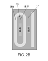
図2bは、グレーレベルSEM画像の例示的な部分を示し、パターンの頂部は明るいグレーであり、底部は暗いグレーである。パターンの明るい頂部は、走査電子ビームによって生じる2次および後方散乱電子によってより多く「照射」され、少なくとも1つのSEM検出器(図示せず)によって検出される。パターンの暗い底部が生じる電子は少なく、したがって同じ検出器によってSEM画像のより暗い部分として検出される。 FIG. 2b shows an exemplary portion of a gray level SEM image, with the top of the pattern being light gray and the bottom being dark gray. The bright apex of the pattern is more "irradiated" by the secondary and backscattered electrons generated by the scanning electron beam and is detected by at least one SEM detector (not shown). Fewer electrons occur at the dark bottom of the pattern, so they are detected by the same detector as darker parts of the SEM image.
パターンは、閉じた楕円形の等高線によって形成される「基準」チャネル16と呼ばれる第1のチャネルを含む。「局所」チャネルと呼ばれる第2のチャネルは、楕円形の等高線とまっすぐな棒状の等高線との間に形成される。
The pattern includes a first channel called the "reference"
モデルの第1のバージョンV=ΔηLR=f(Δh,ΔwLR)は、以下の2つの等式に基づいている。
ηL=η(hL,wL)および
ηR=η(hR,wR)、
上式で、それぞれ、相対グレーレベルの値hLおよびhRが、局所オブジェクトおよび基準オブジェクトに対して測定され、底部チャネルの幅の値wLおよびwRが、局所オブジェクトおよび基準オブジェクトに対してそれぞれ測定される。
The first version of the model V = Δη LR = f (Δh, Δw LR ) is based on the following two equations.
η L = η (h L , w L ) and η R = η (h R , w R ),
In the above equation, the relative gray level values h L and h R are measured for the local and reference objects, and the bottom channel width values w L and w R are for the local and reference objects, respectively. Each is measured.
測定可能な値ΔηLRおよび実際のパラメータΔwLRが計算され、次いで関数「f」を使用してΔhが見出される。関数「f」は、単調であると見なすことができ、較正プロセスを使用して構築することができる。任意の知られている近似を関数「f」に適用するとき、その第1の近似を線形とすることができ、αおよびβと呼ばれる2つの係数/パラメータのみを必要とする。そのような係数は、較正によって見出すことができ、シミュレートすることができ、または事前に選択することができる。 The measurable value Δη LR and the actual parameter Δw LR are calculated and then Δh is found using the function “f”. The function "f" can be considered monotonous and can be constructed using the calibration process. When applying any known approximation to the function "f", the first approximation can be linear and requires only two coefficients / parameters called α and β. Such coefficients can be found by calibration, simulated, or preselected.
したがって、モデルの第1のバージョンは、以下に実質上近接することができる。
ΔηLR=β(Δh)+α(ΔwLR)
上式で、係数αおよびβはそれぞれ、チャネル幅「w」および高さ「h」からの相対グレーレベルηの依存性を特徴付ける。
具体的には、ΔηLR=η(局所)-η(基準)であり、
上式で、η(局所)=Ylocal(bottom)/Ylocal(top)、
η(基準)=Yreference(bottom)/Yreference(top)である。
Yは、パターンの頂部または底部における収率(輝度)を示す。
Therefore, the first version of the model can be substantially close to:
Δη LR = β (Δh) + α (Δw LR )
In the above equation, the coefficients α and β characterize the dependence of the relative gray level η from the channel width “w” and height “h”, respectively.
Specifically, Δη LR = η (local) -η (reference), and
In the above equation, η (local) = Y local (bottom) / Y local (top) ,
η (reference) = Y reference (bottom) / Y reference (top) .
Y indicates the yield (luminance) at the top or bottom of the pattern.
特有の測定に対して選択される局所チャネルおよび基準チャネルは、SEM画像上で互いからかなり離れて位置することができ、各チャネルは、その対応する壁部分に関連付けられ、したがってチャネルの底部および頂部を形成することを理解されたい。さらに、提案される技法の場合、チャネルのうちの一方(たとえば、基準チャネル)は、その実際の測定によって表す必要がない。たとえば、基準チャネルは、測定のプロセスで取得される平均値によって表すことができる。 The local and reference channels selected for specific measurements can be located well away from each other on the SEM image, and each channel is associated with its corresponding wall portion, thus the bottom and top of the channel. Please understand that it forms. Moreover, for the proposed technique, one of the channels (eg, the reference channel) need not be represented by its actual measurement. For example, the reference channel can be represented by an average value obtained during the measurement process.
局所チャネル-基準チャネルの方法論を使用して、コア-ギャップペアの高低差を測定することができ、コアトレンチはギャップトレンチと交互に配置される。図2Cは、半導体ウエハ上の何らかの周期的な構造に属するコアおよびギャップトレンチのグレーレベル等高線を含むパターンからのSEM画像の例示的な部分を示す。この図では、隣接するトレンチの各対が、1つのコアトレンチ18および1つのギャップトレンチ19を含む。上記で論じた一般的な基準チャネル-局所チャネルモデルと比較すると、コアトレンチを基準チャネルとして使用することができ、ギャップトレンチを局所チャネルとして使用することができ、または逆も同様である。本譲受人が所有する米国特許第8,538,130号は、半導体ウエハ上に製作された周期的な構造におけるコア-ギャップペアを含む類似の構造要素を分類するCD計量システムおよび方法について記載している。
The height difference of the core-gap pair can be measured using the local channel-reference channel methodology, with the core trenches alternating with the gap trenches. FIG. 2C shows an exemplary portion of an SEM image from a pattern containing gray level contours of cores and gap trenches belonging to some periodic structure on a semiconductor wafer. In this figure, each pair of adjacent trenches includes one
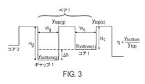
図3は、図2Cに示す周期的な構造の例示的な概略側面図(または断面図)であり、コアトレンチ18よりギャップトレンチ19が深く、コアトレンチとギャップトレンチとの間に典型的な材料凹部(Δhまたは高低差)が存在することを確認することができる。材料凹部は通常、複数パターニング技法(2重パターニングなど)の結果である。ギャップトレンチは高さHgを有し、高さHgは、コアトレンチの高さHcより大きい。それぞれのギャップトレンチおよびコアトレンチの幅WgおよびWcも異なってよい。
FIG. 3 is an exemplary schematic side view (or cross-sectional view) of the periodic structure shown in FIG. 2C, where the
底部におけるグレーレベル輝度(ybottom)と頂部における輝度(ytop)との間の比ηは、1対の隣接するギャップおよびコアトレンチ(たとえば、例示的なペア1)に対して2回測定される。これらの測定された比は、隣接するギャップおよびコアトレンチの異なる高さのために異なる。 The ratio η between the gray level brightness at the bottom (y bottom ) and the brightness at the top (y top ) is measured twice for a pair of adjacent gaps and core trenches (eg, exemplary pair 1). To. These measured ratios vary due to the different heights of adjacent gaps and core trenches.
このケースに対するモデルの提案される第1のバージョンの線形関数は、次のように表現される。
Δηcg=β(Δh)+α(Δwcg)
上式で、Δηcgは、コア-ギャップペアに対する輝度比(すなわち、頂部における輝度(ytop)と底部における輝度(ybottom)との間の比)の差であり、Δhは、コア-ギャップペアに対する高低差であり、Δwcgは、コア-ギャップペアに対する幅差である。αおよびβは、事前に選択されまたは測定/較正から統計的に計算された係数である。上式に示す線形関係により、事前に受け取ったまたはシミュレーションおよび/もしくは較正によって導出された係数αおよびβを考慮に入れながら、SEM画像を使用して輝度(ytop(c)、ybottom(c)、ytop(g)、およびybottom(g))ならびに幅(WcおよびWg)の測定に基づいてΔhを計算することが可能になる。係数αは、トレンチの幅からのηの依存性(dη/dw)を表現する。係数βは、トレンチの高さからのηの依存性(dη/dh)を反映する。
The proposed first version of the linear function of the model for this case is expressed as:
Δη cg = β (Δh) + α (Δw cg )
In the above equation, Δη cg is the difference in the brightness ratio to the core-gap pair (ie, the ratio between the brightness at the top (y top ) and the brightness at the bottom (y bottom )), and Δh is the core-gap. The height difference with respect to the pair, and Δw cg is the width difference with respect to the core-gap pair. α and β are preselected or statistically calculated coefficients from measurements / calibrations. Luminance (y top (c) , y bottom ( c) using SEM images, taking into account the coefficients α and β received in advance or derived by simulation and / or calibration due to the linear relationship shown in the above equation. ) , Y top (g) , and y bottom (g) ) and widths (W c and W g ) can be calculated based on the measurements. The coefficient α represents the dependence of η from the width of the trench (dη / dw). The coefficient β reflects the dependence of η from the height of the trench (dη / dh).
図4は、上述したモデルのバージョンを使用して隣接するコアトレンチとギャップトレンチとの間の高低差を判定する例示的な方法の流れ図である。本出願では、周期的なパターンにおける隣接するコアトレンチおよびギャップトレンチについて繰り返し述べている。しかしこの方法は、本開示の範囲内で、不規則なパターン内の2つのチャネルのΔhを測定するように修正することができ、これら2つのチャネルは、「1対」のギャップ-コアと見なされる。図4の方法は、ハードウェア(たとえば、処理デバイス、回路、専用論理、プログラム可能な論理、マイクロコード、デバイスのハードウェア、集積回路など)、ソフトウェア(たとえば、処理デバイス上で走行もしくは実行される命令)、またはこれらの組合せを含むことができる処理論理によって実施することができる。いくつかの実施形態では、図4の方法は、図1Aおよび図1Bに示すシステムによって実施することができる。 FIG. 4 is a flow chart of an exemplary method for determining the height difference between adjacent core trenches and gap trenches using a version of the model described above. The present application reiterates adjacent core trenches and gap trenches in a periodic pattern. However, within the scope of the present disclosure, this method can be modified to measure the Δh of two channels in an irregular pattern, and these two channels are considered as a “pair” gap-core. Is done. The method of FIG. 4 is run or executed on hardware (eg, processing device, circuit, dedicated logic, programmable logic, microcode, device hardware, integrated circuit, etc.), software (eg, processing device). It can be carried out by an instruction) or a processing logic that can include a combination thereof. In some embodiments, the method of FIG. 4 can be carried out by the system shown in FIGS. 1A and 1B.
図4に示すように、この方法は、ウエハW上にパターンを有するサンプルを1次電子のビームによって走査するブロック20から始めることができる。ブロック22で、SEMの1つまたは複数の検出器が、後方散乱および2次電子を検出する。この検出器データに基づいて、ウエハの1つまたは複数のSEM画像がSEMによって作成される。ブロック24で、1つまたは複数のSEM画像を組み合わせて、複合SEM画像を作成する。ブロック26で、各コア-ギャップペアの幅が測定され、それらの幅差が計算される。この関数は、測定モジュールMMで実施することができる。ブロック28で、各コア-ギャップペアに対して、底部および頂部においてグレーレベルが測定され、ギャップおよびコアに対するηを計算し、次いでΔηを計算する。各コア-ギャップペアに対するηおよびΔηを計算する際、グレーレベルの実施された測定に基づいて、関心領域に対して平均化を行うことができる。最後に、ブロック30で、V=f(Δh)に対するモデルの第1のバージョンを使用して、高低差Δhが導出され、関数fは、Δηcg=β(Δh)+α(Δwcg)として表現される。具体的には、Δh=(Δηcg-αΔwcg)/βである。
As shown in FIG. 4, this method can start with
上述した測定可能な値および実際のパラメータは、絶対値であっても平均値であってもよいことに留意されたい。これらの値は、特有の2つのチャネルに対する絶対値であり、パターンの特有の領域に対して平均化することができる。相対グレーレベル(または輝度)ηは、絶対値であっても平均値であってもよい。絶対値ηは、特有のコア-ギャップペア内の特有のギャップ/コアに対して測定(計算)することができ、平均値ηは、周期的な構造の関心領域内の1群のギャップ/コア/ペアに対して測定(計算)することができる。 Note that the measurable values and actual parameters described above may be absolute or mean. These values are absolute values for the two unique channels and can be averaged for the unique regions of the pattern. The relative gray level (or brightness) η may be an absolute value or an average value. The absolute value η can be measured (calculated) for a unique gap / core within a unique core-gap pair, and the average value η is a group of gaps / cores within the region of interest of the periodic structure. / Can be measured (calculated) for a pair.
同様に、SEM画像上の(1つのコア-ギャップペアの)コアトレンチの幅「wc」および隣接するギャップトレンチの幅「wg」の測定によって取得されるとき、実際のパラメータ「Δwcg」は絶対値であり、関心領域に対して計算される場合、「Δwcg」は、複数の絶対パラメータ「Δwcg」に基づいて平均化される。材料凹部「Δh」は、特有のコア-ギャップペアに対して測定されるときは絶対値であり、関心領域に対して(複数の絶対値「Δh」に基づいて、または平均値「Δwcg」に基づいて)計算されたときは平均値である。さらに、「統計的測定」という用語は、たとえば、実際の測定によって取得される経験的データを使用する較正、または単に平均化された実際の測定であると理解することができる。 Similarly, the actual parameter "Δw cg " when obtained by measuring the width "w c " of the core trench (of one core-gap pair) and the width "w g " of the adjacent gap trenches on the SEM image. Is an absolute value, and when calculated for the region of interest, "Δw cg " is averaged based on a plurality of absolute parameters "Δw cg ". The material recess "Δh" is an absolute value when measured for a unique core-gap pair and is for a region of interest (based on multiple absolute values "Δh" or an average value "Δw cg ". When calculated (based on), it is an average value. Further, the term "statistical measurement" can be understood as, for example, a calibration using empirical data obtained by an actual measurement, or simply an averaged actual measurement.
モデルのバージョン2:電子ビームの傾斜角度を変動させることによる高低差の判定
モデルの第2のバージョンでは、走査電子ビームの傾斜角度が変化したときのSEM画像上の2つの特性点間の測定距離の変化の点から表現することができる変数から高低差を計算する。パターンの側面図の「特性点」は、同じパターンの上面図の「特性線」に対応することができ、2つの特性点間の距離は、2つの平行な特性線間の距離に対応することが、当業者には理解されよう。
Model version 2: Judgment of height difference by varying the tilt angle of the electron beam In the second version of the model, the measurement distance between two characteristic points on the SEM image when the tilt angle of the scanning electron beam changes. The height difference is calculated from the variables that can be expressed from the point of change of. The "characteristic points" in the side view of the pattern can correspond to the "characteristic lines" in the top view of the same pattern, and the distance between the two characteristic points corresponds to the distance between the two parallel characteristic lines. However, it will be understood by those skilled in the art.
特性線は、周期的な構造の下縁部に沿って位置決めされたストリップの形の明るいスポットであると理解されたい。実際には、そのような特性線は、構造の底部と壁との間の底隅部に沿って見出され、隅部には、傾斜した走査電子ビームが到達し、したがって隅部の壁部分および底部の両方からの電子の放出により、SEM画像に比較的明るい(特性)スポットが作成される。 It should be understood that the characteristic lines are bright spots in the form of strips positioned along the lower edge of the periodic structure. In practice, such characteristic lines are found along the bottom corner between the bottom of the structure and the wall, where the tilted scanning electron beam reaches, thus the wall portion of the corner. The emission of electrons from both the bottom and the bottom creates relatively bright (characteristic) spots in the SEM image.
図5は、図2Cおよび図3に示す同じパターンの側面図を示し、より現実的な丸い等高線を有する。パターンは、第1に、ウエハの表面に垂直な軸(点線)に対して傾斜角度γ1を有する電子ビーム40によって走査される。次いでパターンは、γ1とは異なるγ2だけ傾斜した電子ビーム42によって走査することができる。この前提条件は、両方の角度に対して、少なくとも1つの検出器D1が、ギャップトレンチの底隅部(Cg)およびその隣接するコアトレンチの底隅部Ccの両方で特性線を登録し、ギャップおよびコアトレンチは、ここでペア1として示す同じコア-ギャップペアに属することである。CgおよびCcにおける特性線は、D1によって収集されたデータから取得したSEM画像上で明るいスポットとして見られる。これらの線は、傾斜角度が変化すると位置を変化させる。これは、図6により詳細に示されている。追加の条件は、少なくとも1つの検出器が、その検出器のSEM画像を比較し、それらのSEM画像上の距離ΔX1およびΔX2を測定するために、傾斜角度γ1およびγ2の両方に対する特性線を登録することができるべきであることである。
FIG. 5 shows side views of the same pattern shown in FIGS. 2C and 3 with more realistic round contour lines. The pattern is first scanned by an
次いで、同じコア-ギャップペアの異なる傾斜角度に対して取得され、CcおよびCgにおける特性線間で測定された距離ΔX1およびΔX2を使用して、そのコア-ギャップペアの材料凹部Δhを計算する。 The material recess Δh of the core-gap pair is then calculated using the distances ΔX1 and ΔX2 obtained for different tilt angles of the same core-gap pair and measured between the characteristic lines at Cc and Cg.
図6は、図2Cおよび図5に示すパターンのSEM画像の簡略化された概略部分を示し、異なる傾斜角度で生じる特性線が、規則的な構造の明るいグレーの頂部と暗いグレーの底部との間の白色部分として概略的に示されている。γ1<γ2であるため、傾斜角度γ1の特性線はより狭く見え、傾斜角度γ2の特性線はより広く見える。傾斜方向は、太い矢印によって概略的に示されている。距離ΔXは、特有のコア-ギャップペアに対して、特性線の右端間で測定される(右端部は、黒い破線によって表される)。浅いコアにおける特性線は、より深いギャップにおける特性線より広いことに留意されたい。 FIG. 6 shows a simplified schematic portion of the SEM image of the pattern shown in FIGS. 2C and 5, with characteristic lines occurring at different tilt angles at the top of the light gray and the bottom of the dark gray with a regular structure. It is shown schematically as a white area in between. Since γ1 <γ2, the characteristic line of the inclination angle γ1 looks narrower and the characteristic line of the inclination angle γ2 looks wider. The tilt direction is schematically indicated by a thick arrow. The distance ΔX is measured between the right ends of the characteristic line for the unique core-gap pair (the right end is represented by the black dashed line). Note that the characteristic lines in shallow cores are wider than the characteristic lines in deeper gaps.
たとえば、距離ΔX1は、コア-ギャップペア1(コア1およびギャップ1)に対して、傾斜角度γ1で取得されたSEM画像上に見られる特性線間で測定される。距離ΔX2は、同じコア-ギャップペア1に対して、傾斜角度γ2で取得されたSEM画像上に見られる特性線間で測定される。別のコア-ギャップペア(たとえば、ギャップ1およびコア2を含むペア2)に対して、類似の距離を測定することができる。距離ΔXは、傾斜角度を変化させるとともに変化することを見ることができる。その変化は、コア-ギャップペア間の高低差の関数であるため、モデルの適切なバージョンを使用して、ΔXから高低差を導出することができる。
For example, the distance ΔX1 is measured for the core-gap pair 1 (
前述の測定可能な値Δ(ΔX)は、走査電子ビームの2つの異なる傾斜角度γに対して取得された2つのそれぞれのSEM画像を使用して測定された距離(ΔX)の2つの値から計算することができることを理解されたい。たとえば、特有の「コア-ギャップ」ペアに対して2つの傾斜角度を選択することができ、値Δ(ΔX)を取得することができる。 The aforementioned measurable value Δ (ΔX) is from two values of distance (ΔX) measured using two respective SEM images acquired for two different tilt angles γ of the scanning electron beam. Please understand that it can be calculated. For example, two tilt angles can be selected for a unique "core-gap" pair and the value Δ (ΔX) can be obtained.
図7は、モードのバージョン2に応じて方法を実施する例示的な流れ図である。図7の方法は、ハードウェア(たとえば、処理デバイス、回路、専用論理、プログラム可能な論理、マイクロコード、デバイスのハードウェア、集積回路など)、ソフトウェア(たとえば、処理デバイス上で走行もしくは実行される命令)、またはこれらの組合せを含むことができる処理論理によって実施することができる。また、パターンは、材料凹部を有する周期的な構造であっても不規則な構造であってもよい。いくつかの実施形態では、図4の方法は、図1Aおよび図1Bに示すシステムによって実施することができる。このモデルを実施するために少なくとも1つの検出器が必要であることに留意されたい。
FIG. 7 is an exemplary flow chart that implements the method according to
図7の方法は、2つの傾斜角度γ1およびγ2における1次電子のビームによってパターンを走査するブロック50から始まる。次に、ブロック52で、1つまたは複数の検出器によって2次および後方散乱電子が検出され、それによって各傾斜角度に対する対応するSEM画像が作成される。SEM画像は、複数の検出器からのデータを使用して複合画像とすることができることに留意されたい。ブロック54で、特有の傾斜角度に対して取得された各SEM画像に対して、各コア-ギャップペアに対してその特有の傾斜角度で作成された特性線が識別される。ブロック56で、特有の各コア-ギャップペアに対して、2つの異なる傾斜角度における特性線間の距離ΔX1およびΔX2が測定される。その後、そのような距離間の差、すなわちΔ(ΔX)が計算される。ブロック58で、モデルのバージョン2の関数を使用してΔhが計算され、変数Δ(ΔX)は、等式Δ(ΔX)=(Δ(tgγ))*Δhに示すように、Δhの関数であり、上式で、(Δ(tgγ))はV=f(Δh)における関数「f」であり、傾斜角度の変化を反映する。
The method of FIG. 7 begins with
要約すると、モデルの第2のバージョンで測定可能な値Vを測定する方法は、たとえば、
- 電子ビームに対して2つの異なる角度を角度γ1およびγ2として選択し、第3の実際のパラメータΔtgγを(tg(γ1)-tg(γ2))として計算することによって、関数「f」の2つの実際のパラメータを選択するサブステップと、
- 角度γ1、次いで角度γ2で傾斜した電子ビームによって、規則的な構造を走査するサブステップと、
- 2つのそれぞれの異なる角度γ1およびγ2に対するパターンの2つのSEM画像Iγ1およびIγ2を取得するサブステップと、
- 2つの画像Iγ1およびIγ2のそれぞれに対して、1対のチャネル(たとえば、隣接するコアおよびギャップトレンチ)の2つの特性線を判定するサブステップと(2つの特性線は、傾斜した電子ビームによって照射されたときにその対の隣接するコアおよびギャップトレンチの底隅部CcおよびCgによって前記画像上に作成された特性線である)、
- 2つの画像Iγ1およびIγ2のそれぞれに対して、その対のチャネルの2つの特性線間の距離ΔXを判定するサブステップと、
- 画像Iγ1で判定された距離ΔXと画像Iγ2で判定された距離ΔXとの間の差Δ(ΔX)として値Vを測定するサブステップとを含むことができる。
In summary, the method of measuring the measurable value V in the second version of the model is, for example,
-By selecting two different angles with respect to the electron beam as angles γ1 and γ2 and calculating the third actual parameter Δtgγ as (tg (γ1) -tg (γ2)), the function “f” 2 A substep to select one actual parameter, and
-A sub-step that scans a regular structure with an electron beam tilted at angle γ1 and then at angle γ2.
-A sub-step to acquire two SEM images Iγ1 and Iγ2 of the pattern for two different angles γ1 and γ2, respectively.
-For each of the two images Iγ1 and Iγ2, a substep to determine the two characteristic lines of a pair of channels (eg, adjacent cores and gap trenches) and (the two characteristic lines are due to an inclined electron beam). Characteristic lines created on the image by the bottom corners Cc and Cg of the pair of adjacent cores and gap trenches when irradiated),.
-For each of the two images Iγ1 and Iγ2, a substep for determining the distance ΔX between the two characteristic lines of the paired channel,
-A substep of measuring the value V as the difference Δ (ΔX) between the distance ΔX determined by the image Iγ1 and the distance ΔX determined by the image Iγ2 can be included.
次いで、高低差ΔhがΔh=Δ(ΔX)/(Δ(tgγ))として判定され、上式で、Δtgγ=tg(γ1)-tg(γ2)である。 Next, the height difference Δh is determined as Δh = Δ (ΔX) / (Δ (tgγ)), and in the above equation, Δtgγ = tg (γ1) −tg (γ2).
ウエハの周期的な構造上で関心領域を選択することができ、次いで関心領域内で事前選択された1つまたは複数の軸/方向に沿って、絶対測定値(および/または絶対測定値に基づいて得られた絶対計算値)を平均化することができる。これにより、測定値の精度と、ウエハの特定の領域またはウエハ全体における高低差の適切な推定との間にトレードオフが導入される。 Regions of interest can be selected on the periodic structure of the wafer and then along one or more preselected axes / directions within the region of interest, based on absolute measurements (and / or absolute measurements). The absolute calculated value obtained) can be averaged. This introduces a trade-off between the accuracy of the measurements and the proper estimation of the height difference over a particular region of the wafer or across the wafer.
図8は、コンピュータシステム600の例示的な機械を示し、コンピュータシステム600において、本明細書に論じる方法のうちのいずれか1つまたは複数を機械に実施させる1組の命令を実行することができる。代替の実装では、機械は、LAN、イントラネット、エクストラネット、および/またはインターネット内の他の機械に接続(たとえば、ネットワーク化)することができる。機械は、クライアント-サーバネットワーク環境においてサーバまたはクライアント機械の容量内で、ピアツーピア(もしくは分散型)ネットワーク環境内のピア機械として、またはクラウドコンピューティングインフラストラクチャもしくは環境内のサーバもしくはクライアント機械として動作することができる。
FIG. 8 illustrates an exemplary machine of
機械は、パーソナルコンピュータ(PC)、タブレットPC、セットトップボックス(STB)、パーソナルデジタルアシスタント(PDA)、セルラー電話、ウェブアプライアンス、サーバ、ネットワークルータ、スイッチもしくはブリッジ、またはその機械によって実施されるべき動作を指定する1組の命令を(順次もしくはその他で)実行することが可能な任意の機械とすることができる。さらに、単一の機械が示されているが、「機械」という用語はまた、本明細書に論じる方法のうちのいずれか1つまたは複数を実施するために1組(または複数組)の命令を個別または集合的に実行する任意の1群の機械を含むと解釈されたい。 The machine is a personal computer (PC), tablet PC, set-top box (STB), personal digital assistant (PDA), cellular phone, web appliance, server, network router, switch or bridge, or the operation to be performed by the machine. It can be any machine capable of executing a set of instructions (sequentially or otherwise). Further, although a single machine is shown, the term "machine" also refers to a set (or set) of instructions to implement any one or more of the methods discussed herein. Should be interpreted as including any set of machines that perform individually or collectively.
例示的なコンピュータシステム600は、バス608を介して互いに通信する処理デバイス602、主メモリ604(たとえば、読取り専用メモリ(ROM)、フラッシュメモリ、シンクロナスDRAM(SDRAM)などのダイナミックランダムアクセスメモリ(DRAM)など)、スタティックメモリ606(たとえば、フラッシュメモリ、スタティックランダムアクセスメモリ(SRAM)など)、およびデータ記憶デバイス616を含む。
An
処理デバイス602は、マイクロプロセッサ、中央処理装置などの1つまたは複数の汎用処理デバイスを表す。より詳細には、処理デバイスは、複合命令セットコンピューティング(CISC)マイクロプロセッサ、縮小命令セットコンピューティング(RISC)マイクロプロセッサ、超長命令語(VLIW)マイクロプロセッサ、または他の命令セットを実施するプロセッサ、もしくは命令セットの組合せを実施するプロセッサとすることができる。処理デバイス602はまた、特定用途向け集積回路(ASIC)、フィールドプログラマブルゲートアレイ(FPGA)、デジタル信号プロセッサ(DSP)、ネットワークプロセッサなどの1つまたは複数の特定目的処理デバイスとすることができる。処理デバイス602は、本明細書に論じる動作およびステップを実施する命令を実施するように構成される。 The processing device 602 represents one or more general purpose processing devices such as a microprocessor, a central processing unit, and the like. More specifically, the processing device is a compound instruction set computing (CISC) microprocessor, a reduced instruction set computing (RISC) microprocessor, a very long instruction word (VLIW) microprocessor, or a processor that implements another instruction set. , Or it can be a processor that implements a combination of instruction sets. The processing device 602 can also be one or more special purpose processing devices such as application specific integrated circuits (ASICs), field programmable gate arrays (FPGAs), digital signal processors (DSPs), network processors and the like. The processing device 602 is configured to perform instructions to perform the operations and steps discussed herein.
コンピュータシステム600は、ネットワーク618を介して通信するネットワークインターフェースデバイス622をさらに含むことができる。コンピュータシステム600はまた、ビデオ表示ユニット610(たとえば、液晶ディスプレイ(LCD)またはカソードレイチューブ(CRT))、英数字入力デバイス612(たとえば、キーボード)、カーソル制御デバイス614(たとえば、マウスまたはタッチパッド))、信号生成デバイス620(たとえば、スピーカ)、グラフィックス処理ユニット(図示せず)、ビデオ処理ユニット(図示せず)、および音声処理ユニット(図示せず)を含むことができる。
The
データ記憶デバイス616は、機械可読記憶媒体624(コンピュータ可読媒体としても知られている)を含むことができ、機械可読記憶媒体624上には、本明細書に記載する方法または関数のうちのいずれか1つまたは複数を実施する1組もしくは複数組の命令またはソフトウェアが記憶される。これらの命令はまた、コンピュータシステム600によるその実行中、主メモリ604および/または処理デバイス602内に完全にまたは少なくとも部分的に常駐することができ、主メモリ604および処理デバイス602はまた、機械可読記憶媒体を構成する。
The
1つの実装では、これらの命令は、高低差判定に対応する機能を実施する命令を含む。機械可読記憶媒体624は、例示的な実装では、単一の媒体であるものとして示されているが、「機械可読記憶媒体」という用語は、1組もしくは複数組の命令を記憶する単一の媒体または複数の媒体(たとえば、集中型もしくは分散型のデータベース、ならびに/または付随するキャッシュおよびサーバ)を含むと解釈されるべきである。「機械可読記憶媒体」という用語はまた、機械による実行のために1組の命令を記憶または符号化することが可能であり、本開示の方法のうちのいずれか1つまたは複数を機械に実施させる任意の媒体を含むと解釈されるものとする。したがって、「機械可読記憶媒体」という用語は、それだけに限定されるものではないが、固定メモリ、光媒体、および磁気媒体を含むと解釈されるものとする。
In one implementation, these instructions include instructions that perform the function corresponding to the height difference determination. Although the machine-
前述の詳細な説明のいくつかの部分について、コンピュータメモリ内のデータビットに関する動作のアルゴリズムおよび記号表現の点から提示した。これらのアルゴリズムの説明および表現は、機能の本質を当業者に最も効果的に伝えるために、データ処理技術の当業者によって使用される方法である。ここでアルゴリズムは、全体として、所望の結果をもたらす自己矛盾のない動作シーケンスであると考えられる。これらの動作は、物理量の物理的な操作を必要とする動作である。通常、必須ではないが、これらの量は、記憶、結合、比較、およびその他の方法で操作することが可能である電気または磁気信号の形をとる。主に一般的な使用の理由で、これらの信号をビット、値、要素、記号、文字、用語、数字などと呼ぶことが時として好都合であることが分かっている。 Some parts of the above detailed description are presented in terms of algorithms and symbolic representations of operation for data bits in computer memory. Descriptions and representations of these algorithms are methods used by those skilled in the art of data processing techniques to best convey the essence of functionality to those skilled in the art. Here, the algorithm as a whole is considered to be a self-consistent sequence of operations that yields the desired result. These operations are operations that require physical manipulation of physical quantities. Usually not required, these quantities take the form of electrical or magnetic signals that can be stored, coupled, compared, and otherwise manipulated. It has sometimes been found convenient to refer to these signals as bits, values, elements, symbols, letters, terms, numbers, etc., primarily for general use.
しかし、上記および類似の用語はすべて、適当な物理量に関連付けられるべきであり、これらの量に適用される単に好都合な名称であることに留意されたい。上記の議論から明らかであると別途具体的に指示しない限り、本説明全体を通して、「識別」または「判定」または「実行」または「実施」または「収集」または「作成」または「送信」などの用語を利用する議論は、コンピュータシステムのレジスタおよびメモリ内で物理(電子)量として表されるデータを操作し、コンピュータシステムメモリもしくはレジスタまたは他のそのような情報記憶デバイス内で物理量として同様に表される他のデータに変換する、コンピュータシステムまたは類似の電子コンピューティングデバイスの動作およびプロセスを指すことを理解されたい。 However, it should be noted that all of the above and similar terms should be associated with appropriate physical quantities and are merely convenient names that apply to these quantities. Throughout this description, such as "identification" or "judgment" or "execution" or "implementation" or "collection" or "creation" or "transmission", unless otherwise specifically indicated as is evident from the above discussion. Discussions that utilize the term manipulate data represented as physical (electronic) quantities in computer system registers and memory, as well as in computer system memory or registers or other such information storage devices. It should be understood that it refers to the behavior and process of a computer system or similar electronic computing device that is converted into other data.
本開示はまた、本明細書の動作を実施する装置に関する。この装置は、所期の目的のために特別に構築することができ、またはコンピュータ内に記憶されているコンピュータプログラムによって選択的に起動もしくは再構成される汎用コンピュータを備えることができる。そのようなコンピュータプログラムは、それだけに限定されるものではないが、フロッピーディスク、光ディスク、CD-ROM、および磁気光学ディスク、読取り専用メモリ(ROM)、ランダムアクセスメモリ(RAM)、EPROM、EEPROM、磁気もしくは光カード、または電子命令を記憶するのに適した任意のタイプの媒体を含む任意のタイプのディスクなど、コンピュータ可読記憶媒体内に記憶することができ、各媒体は、コンピュータシステムバスに結合される。 The present disclosure also relates to an apparatus that carries out the operations of the present specification. The device can be specially constructed for the intended purpose, or can include a general purpose computer that is selectively started or reconfigured by a computer program stored in the computer. Such computer programs are, but are not limited to, floppy disks, optical disks, CD-ROMs, and magnetic optical disks, read-only memory (ROM), random access memory (RAM), EPROM, EEPROM, magnetic or Each medium can be stored in a computer-readable storage medium, such as an optical card, or any type of disk, including any type of medium suitable for storing electronic instructions, and each medium is coupled to a computer system bus. ..
本明細書に提示するアルゴリズムおよびディスプレイは、いかなる特定のコンピュータまたは他の装置にも本質的に関係するものではない。本明細書の教示によるプログラムとともに様々な汎用システムを使用することができ、またはこの方法を実施するためにより特殊な装置を構築するのに好都合であると実証することができる。様々なこれらのシステムに対する構造について、以下の説明に記載されている。加えて、本開示は、何らかの特定のプログラミング言語を参照するものとして記載されていない。本明細書に記載する本開示の教示を実施するために、様々なプログラミング言語を使用することができることが理解されよう。 The algorithms and displays presented herein are not inherently relevant to any particular computer or other device. Various general-purpose systems can be used with the programs as taught herein, or can be demonstrated to be convenient for constructing more specialized devices for carrying out this method. The structure for these various systems is described in the description below. In addition, this disclosure is not described as referring to any particular programming language. It will be appreciated that various programming languages can be used to carry out the teachings of the present disclosure described herein.
本開示は、命令が記憶された機械可読媒体を含むことができるコンピュータプログラム製品またはソフトウェアとして提供することができ、これらの命令は、本開示によるプロセスを実施するようにコンピュータシステム(または他の電子デバイス)をプログラムするために使用することができる。機械可読媒体は、機械(たとえば、コンピュータ)によって可読の形式で情報を記憶する任意の機構を含む。たとえば、機械可読(たとえば、コンピュータ可読)媒体には、読取り専用メモリ(「ROM」)、ランダムアクセスメモリ(「RAM」)、磁気ディスク記憶媒体、光記憶媒体、フラッシュ記憶デバイスなどの機械(たとえば、コンピュータ)可読記憶媒体が含まれる。 The present disclosure may be provided as a computer program product or software that may include a machine-readable medium in which the instructions are stored, and these instructions may be used in a computer system (or other electronic device) to carry out the process according to the present disclosure. Can be used to program a device). Machine-readable media include any mechanism that stores information in a form readable by a machine (eg, a computer). For example, machine-readable (eg, computer-readable) media include machines such as read-only memory (“ROM”), random access memory (“RAM”), magnetic disk storage media, optical storage media, and flash storage devices (eg, flash storage devices). Computer) Includes readable storage media.
上記の明細書では、本開示の実装について、本開示の特有の例示的な実装を参照して説明した。以下の特許請求の範囲に記載する本開示の実装のより広い趣旨および範囲から逸脱することなく、様々な修正を加えることができることが明らかである。したがって、本明細書および図面は、限定ではなく例示であると見なされるべきである。 In the above specification, the implementation of the present disclosure has been described with reference to the specific exemplary implementation of the present disclosure. It is clear that various modifications can be made without departing from the broader intent and scope of the implementation of this disclosure described in the claims below. Therefore, the specification and drawings should be considered as illustrative, not limited.
Claims (20)
前記高低差の関数として表現される変数を有するモデルを識別するステップであって、前記関数が1つまたは複数の物理パラメータと、前記1つまたは複数の物理パラメータの相互依存性を特徴付ける1つまたは複数の量とを有する、識別するステップと、
前記半導体ウエハ上の前記パターンの実際の画像上で測定を実施して、前記高低差の前記関数の前記1つまたは複数の物理パラメータの値を取得するステップと、
コンピュータプロセッサによって、前記取得した1つまたは複数の物理パラメータの値と、前記1つまたは複数の物理パラメータの相互依存性を特徴付ける前記1つまたは複数の量とを使用して前記モデルから前記高低差を判定するステップとを含む方法。 A computer implementation method for determining the height difference between two features in a pattern on a semiconductor wafer.
A step of identifying a model having a variable represented as a function of height difference, wherein the function characterizes the interdependence of one or more physical parameters and the one or more physical parameters. With multiple quantities, with the identification step,
A step of performing a measurement on an actual image of the pattern on the semiconductor wafer to obtain the value of the one or more physical parameters of the function of the height difference.
The height difference from the model using the value of the one or more physical parameters obtained by the computer processor and the one or more quantities that characterize the interdependence of the one or more physical parameters. A method that includes a step to determine.
コアトレンチとギャップトレンチとの間の前記高低差の関数として表現される変数を有するモデルを識別するステップであって、前記関数が1つまたは複数の物理パラメータと、前記1つまたは複数の物理パラメータの相互依存性を特徴付ける1つまたは複数の量とを有する、識別するステップと、
前記周期的な構造の実際の画像上で測定を実施して、前記高低差の前記関数の前記1つまたは複数の物理パラメータの値を取得するステップと、
コンピュータプロセッサによって、前記取得した1つまたは複数の物理パラメータの値と、前記1つまたは複数の物理パラメータの相互依存性を特徴付ける前記1つまたは複数の量とを使用して前記モデルから前記高低差を判定するステップとを含む方法。 The height difference between the core trench and the gap trench in the periodic structure is determined, and the periodic structure includes a plurality of core trenches and a plurality of gap trenches formed on the semiconductor wafer by a computer implementation method. There,
A step of identifying a model having a variable represented as a function of the height difference between a core trench and a gap trench, wherein the function has one or more physical parameters and the one or more physical parameters. With the step of identifying, having one or more quantities that characterize the interdependence of
A step of making measurements on an actual image of the periodic structure to obtain the values of the one or more physical parameters of the function of the height difference.
The height difference from the model using the value of the one or more physical parameters obtained by the computer processor and the one or more quantities that characterize the interdependence of the one or more physical parameters. A method that includes a step to determine.
走査電子ビームの第1の傾斜角度で前記周期的な構造を走査して、前記周期的な構造の第1の実際の画像を取得するステップと、
前記走査電子ビームの第2の傾斜角度で前記周期的な構造を走査して、前記周期的な構造の第2の実際の画像を取得するステップであって、前記第2の傾斜角度が前記第1の傾斜角度とは異なる、取得するステップと、
前記第1の実際の画像上で1対の特性点を識別し、前記1対の特性点間の距離を測定するステップと、
前記第2の実際の画像上で前記1対の特性点を識別し、前記1対の前記特性点間の距離を測定するステップと、
前記走査電子ビームの前記第1の傾斜角度および前記第2の傾斜角度の変化に対する、前記第1の実際の画像および前記第2の実際の画像それぞれで測定された前記距離の変化の点から前記モデルの前記変数を表現するステップとをさらに含む、請求項7に記載の方法。 The step of performing the measurement is
A step of scanning the periodic structure at a first tilt angle of the scanning electron beam to obtain a first actual image of the periodic structure.
A step of scanning the periodic structure at a second tilt angle of the scanning electron beam to obtain a second actual image of the periodic structure, wherein the second tilt angle is the second tilt angle. The steps to be acquired and the steps to be acquired, which are different from the tilt angle of 1.
A step of identifying a pair of characteristic points on the first actual image and measuring the distance between the pair of characteristic points.
A step of identifying the pair of characteristic points on the second actual image and measuring the distance between the pair of characteristic points.
From the point of change of the distance measured in each of the first actual image and the second actual image with respect to the change of the first tilt angle and the second tilt angle of the scanning electron beam. 7. The method of claim 7, further comprising the step of representing the variables of the model.
請求項10に記載の方法。 Further including the step of identifying a plurality of pairs of characteristic points on the first and second actual images, each of the pair of characteristic points is created by a corresponding pair of core trenches and gap trenches. ,
The method according to claim 10.
前記複数対の特性点から取得された距離の平均を計算するステップと、
前記距離の平均の変化の点から前記変数を表現するステップとを含む、請求項11に記載の方法。 The step of expressing the variable from the point of change of the distance measured in each of the first actual image and the second actual image is
The step of calculating the average of the distances obtained from the plurality of pairs of characteristic points, and
11. The method of claim 11, comprising the step of expressing the variable in terms of the change in the average of the distances .
Δη=αΔw+βΔh
という線形関数から作成され、上式で、ηはグレーレベル計算の輝度比を示し、Δηはコアトレンチとギャップトレンチとの間のηの差を示し、αおよびβは係数を示し、Δwは幅差であり、Δhはコアトレンチとギャップトレンチとの間の高低差である、請求項14に記載の方法。 The model is
Δη = αΔw + βΔh
In the above equation, η indicates the brightness ratio of the gray level calculation, Δη indicates the difference of η between the core trench and the gap trench, α and β indicate the coefficient, and Δw indicates the width. The method of claim 14, wherein Δh is the height difference between the core trench and the gap trench.
メモリと、
処理デバイスとを備え、前記処理デバイスは、
コアトレンチとギャップトレンチとの間の前記高低差の関数として表現される変数を有するモデルを識別することであって、前記関数が1つまたは複数の物理パラメータと、前記1つまたは複数の物理パラメータの相互依存性を特徴付ける1つまたは複数の量とを有する、識別することと、
前記周期的な構造の実際の画像上で実施された測定から前記高低差の前記関数の前記1つまたは複数の物理パラメータの値を取得することと、
前記取得した1つまたは複数の物理パラメータの値と、前記1つまたは複数の物理パラメータの相互依存性を特徴付ける前記1つまたは複数の量とを使用して前記モデルから前記高低差を判定することとを行うように、前記メモリに動作可能に結合される、システム。 A system for determining the height difference between a core trench and a gap trench in a periodic structure, wherein the periodic structure includes a plurality of core trenches and a plurality of gap trenches formed on a semiconductor wafer. The system
With memory
The processing device comprises a processing device.
Identifying a model that has a variable expressed as a function of the height difference between a core trench and a gap trench, wherein the function is one or more physical parameters and the one or more physical parameters. Having one or more quantities that characterize the interdependence of
Obtaining the values of the one or more physical parameters of the function of the height difference from the measurements made on the actual image of the periodic structure.
Determining the height difference from the model using the obtained values of the one or more physical parameters and the one or more quantities that characterize the interdependence of the one or more physical parameters. A system that is operably coupled to said memory to do so.
Applications Claiming Priority (5)
| Application Number | Priority Date | Filing Date | Title |
|---|---|---|---|
| US201762508312P | 2017-05-18 | 2017-05-18 | |
| US62/508,312 | 2017-05-18 | ||
| US15/982,918 | 2018-05-17 | ||
| US15/982,918 US10748272B2 (en) | 2017-05-18 | 2018-05-17 | Measuring height difference in patterns on semiconductor wafers |
| PCT/US2018/033480 WO2018213758A2 (en) | 2017-05-18 | 2018-05-18 | Measuring height difference in patterns on semiconductor wafers |
Publications (3)
| Publication Number | Publication Date |
|---|---|
| JP2020521325A JP2020521325A (en) | 2020-07-16 |
| JP2020521325A5 JP2020521325A5 (en) | 2021-07-26 |
| JP7026140B2 true JP7026140B2 (en) | 2022-02-25 |
Family
ID=64272391
Family Applications (1)
| Application Number | Title | Priority Date | Filing Date |
|---|---|---|---|
| JP2019563887A Active JP7026140B2 (en) | 2017-05-18 | 2018-05-18 | Measurement of height difference in pattern on semiconductor wafer |
Country Status (6)
| Country | Link |
|---|---|
| US (2) | US10748272B2 (en) |
| JP (1) | JP7026140B2 (en) |
| KR (1) | KR102341667B1 (en) |
| CN (2) | CN115060207B (en) |
| TW (1) | TWI757489B (en) |
| WO (1) | WO2018213758A2 (en) |
Families Citing this family (4)
| Publication number | Priority date | Publication date | Assignee | Title |
|---|---|---|---|---|
| US20220214165A1 (en) * | 2019-05-21 | 2022-07-07 | Applied Materials, Inc. | Enhanced cross sectional features measurement methodology |
| US11530915B2 (en) * | 2019-08-07 | 2022-12-20 | Hitachi High-Tech Corporation | Dimension measuring device, dimension measuring method, and semiconductor manufacturing system |
| CN111816580A (en) * | 2020-07-16 | 2020-10-23 | 宁波江丰电子材料股份有限公司 | Method and system for measuring width of pattern boss of wafer retaining ring |
| CN113594057B (en) * | 2021-08-05 | 2024-02-02 | 上海天岳半导体材料有限公司 | Device, method, equipment and medium for calculating width of atomic step of wafer |
Citations (4)
| Publication number | Priority date | Publication date | Assignee | Title |
|---|---|---|---|---|
| JP2003031631A (en) | 2001-07-13 | 2003-01-31 | Mitsubishi Electric Corp | Method of recognizing side face of pattern and method of detecting and classifying defect |
| WO2011013342A1 (en) | 2009-07-27 | 2011-02-03 | 株式会社日立ハイテクノロジーズ | Pattern evaluation method, device therefor, and electron beam device |
| JP2012519391A (en) | 2009-03-02 | 2012-08-23 | アプライド マテリアルズ イスラエル リミテッド | CD measurement system and method for classifying similar structural elements |
| WO2014175150A1 (en) | 2013-04-22 | 2014-10-30 | 株式会社日立ハイテクノロジーズ | Sample observation device |
Family Cites Families (18)
| Publication number | Priority date | Publication date | Assignee | Title |
|---|---|---|---|---|
| JPH0778267A (en) * | 1993-07-09 | 1995-03-20 | Silicon Graphics Inc | Method for display of shadow and computer-controlled display system |
| JP2006065368A (en) * | 2004-08-24 | 2006-03-09 | Sony Corp | Image display device and method, and computer program |
| JP2007218711A (en) * | 2006-02-16 | 2007-08-30 | Hitachi High-Technologies Corp | Method for measuring measurement target pattern using electron microscope device |
| WO2010065446A2 (en) | 2008-12-01 | 2010-06-10 | The Procter & Gamble Company | Perfume systems |
| JP5500974B2 (en) * | 2009-12-25 | 2014-05-21 | 株式会社日立ハイテクノロジーズ | Pattern measuring device |
| TWI550679B (en) * | 2010-10-26 | 2016-09-21 | 瑪波微影Ip公司 | Modulation device and charged particle multi-beamlet lithography system using the same |
| DE102011079382B4 (en) * | 2011-07-19 | 2020-11-12 | Carl Zeiss Smt Gmbh | Method and device for analyzing and eliminating a defect in an EUV mask |
| US8604427B2 (en) | 2012-02-02 | 2013-12-10 | Applied Materials Israel, Ltd. | Three-dimensional mapping using scanning electron microscope images |
| US8843875B2 (en) * | 2012-05-08 | 2014-09-23 | Kla-Tencor Corporation | Measurement model optimization based on parameter variations across a wafer |
| US9546862B2 (en) * | 2012-10-19 | 2017-01-17 | Kla-Tencor Corporation | Systems, methods and metrics for wafer high order shape characterization and wafer classification using wafer dimensional geometry tool |
| JP2014130077A (en) * | 2012-12-28 | 2014-07-10 | Hitachi High-Technologies Corp | Pattern shape evaluation method, semiconductor device manufacturing method, and pattern shape evaluation device |
| US9679371B2 (en) * | 2013-06-24 | 2017-06-13 | Hitachi High-Technologies Corporation | Pattern shape evaluation device and method |
| US10935893B2 (en) * | 2013-08-11 | 2021-03-02 | Kla-Tencor Corporation | Differential methods and apparatus for metrology of semiconductor targets |
| KR20150085956A (en) | 2014-01-17 | 2015-07-27 | 삼성전자주식회사 | A method of measuring a semiconductor device, a semiconductor measurement system, and a method of a semiconductor device using the same |
| US9484188B2 (en) * | 2015-03-11 | 2016-11-01 | Mapper Lithography Ip B.V. | Individual beam pattern placement verification in multiple beam lithography |
| JP6560052B2 (en) * | 2015-08-03 | 2019-08-14 | 株式会社ディスコ | Adhesion degree detection method |
| US10366200B2 (en) * | 2016-09-07 | 2019-07-30 | Taiwan Semiconductor Manufacturing Company, Ltd. | System for and method of manufacturing a layout design of an integrated circuit |
| US10636140B2 (en) * | 2017-05-18 | 2020-04-28 | Applied Materials Israel Ltd. | Technique for inspecting semiconductor wafers |
-
2018
- 2018-05-17 US US15/982,918 patent/US10748272B2/en active Active
- 2018-05-18 CN CN202210570423.1A patent/CN115060207B/en active Active
- 2018-05-18 CN CN201880032678.4A patent/CN110622289B/en active Active
- 2018-05-18 JP JP2019563887A patent/JP7026140B2/en active Active
- 2018-05-18 TW TW107117023A patent/TWI757489B/en active
- 2018-05-18 KR KR1020197037458A patent/KR102341667B1/en active IP Right Grant
- 2018-05-18 WO PCT/US2018/033480 patent/WO2018213758A2/en active Application Filing
-
2020
- 2020-08-17 US US16/995,077 patent/US11301983B2/en active Active
Patent Citations (4)
| Publication number | Priority date | Publication date | Assignee | Title |
|---|---|---|---|---|
| JP2003031631A (en) | 2001-07-13 | 2003-01-31 | Mitsubishi Electric Corp | Method of recognizing side face of pattern and method of detecting and classifying defect |
| JP2012519391A (en) | 2009-03-02 | 2012-08-23 | アプライド マテリアルズ イスラエル リミテッド | CD measurement system and method for classifying similar structural elements |
| WO2011013342A1 (en) | 2009-07-27 | 2011-02-03 | 株式会社日立ハイテクノロジーズ | Pattern evaluation method, device therefor, and electron beam device |
| WO2014175150A1 (en) | 2013-04-22 | 2014-10-30 | 株式会社日立ハイテクノロジーズ | Sample observation device |
Also Published As
| Publication number | Publication date |
|---|---|
| WO2018213758A2 (en) | 2018-11-22 |
| KR20190143456A (en) | 2019-12-30 |
| US10748272B2 (en) | 2020-08-18 |
| CN110622289B (en) | 2022-05-24 |
| CN115060207B (en) | 2023-07-21 |
| KR102341667B1 (en) | 2021-12-22 |
| CN110622289A (en) | 2019-12-27 |
| CN115060207A (en) | 2022-09-16 |
| US20200380668A1 (en) | 2020-12-03 |
| WO2018213758A3 (en) | 2018-12-27 |
| TWI757489B (en) | 2022-03-11 |
| US20180336675A1 (en) | 2018-11-22 |
| TW201909113A (en) | 2019-03-01 |
| JP2020521325A (en) | 2020-07-16 |
| US11301983B2 (en) | 2022-04-12 |
Similar Documents
| Publication | Publication Date | Title |
|---|---|---|
| JP7026140B2 (en) | Measurement of height difference in pattern on semiconductor wafer | |
| JP2005156436A (en) | Semiconductor pattern measuring method and process control method | |
| CN111987008B (en) | High resolution three-dimensional profile measurement of features in advanced semiconductor devices | |
| US20220214165A1 (en) | Enhanced cross sectional features measurement methodology | |
| JP2020521325A5 (en) | ||
| CN110678968B (en) | Technique for inspecting semiconductor wafers | |
| TWI809703B (en) | Contour analysis device, processing condition determination system, shape estimation system, semiconductor device manufacturing system, search device and data structure used for them | |
| TW201923923A (en) | Determining a critical dimension variation of a pattern | |
| TWI773013B (en) | Pattern inspection device | |
| CN112635342B (en) | Use of an electron beam scanning electron microscope for characterizing a sidewall that is blocked from view by an electron beam | |
| JP7167323B2 (en) | Pattern measuring device and measuring method | |
| JP2007178294A (en) | Edge detection method and edge detection device |
Legal Events
| Date | Code | Title | Description |
|---|---|---|---|
| A521 | Request for written amendment filed |
Free format text: JAPANESE INTERMEDIATE CODE: A523 Effective date: 20210518 |
|
| A621 | Written request for application examination |
Free format text: JAPANESE INTERMEDIATE CODE: A621 Effective date: 20210518 |
|
| A871 | Explanation of circumstances concerning accelerated examination |
Free format text: JAPANESE INTERMEDIATE CODE: A871 Effective date: 20210518 |
|
| A131 | Notification of reasons for refusal |
Free format text: JAPANESE INTERMEDIATE CODE: A131 Effective date: 20210901 |
|
| A521 | Request for written amendment filed |
Free format text: JAPANESE INTERMEDIATE CODE: A523 Effective date: 20211201 |
|
| TRDD | Decision of grant or rejection written | ||
| A01 | Written decision to grant a patent or to grant a registration (utility model) |
Free format text: JAPANESE INTERMEDIATE CODE: A01 Effective date: 20220113 |
|
| A61 | First payment of annual fees (during grant procedure) |
Free format text: JAPANESE INTERMEDIATE CODE: A61 Effective date: 20220214 |
|
| R150 | Certificate of patent or registration of utility model |
Ref document number: 7026140 Country of ref document: JP Free format text: JAPANESE INTERMEDIATE CODE: R150 |