JP7017650B2 - Memory management methods, equipment, and systems - Google Patents
Memory management methods, equipment, and systems Download PDFInfo
- Publication number
- JP7017650B2 JP7017650B2 JP2020569181A JP2020569181A JP7017650B2 JP 7017650 B2 JP7017650 B2 JP 7017650B2 JP 2020569181 A JP2020569181 A JP 2020569181A JP 2020569181 A JP2020569181 A JP 2020569181A JP 7017650 B2 JP7017650 B2 JP 7017650B2
- Authority
- JP
- Japan
- Prior art keywords
- memory
- subsystem
- communication subsystem
- operating system
- addresses
- Prior art date
- Legal status (The legal status is an assumption and is not a legal conclusion. Google has not performed a legal analysis and makes no representation as to the accuracy of the status listed.)
- Active
Links
Images


Classifications
-
- G—PHYSICS
- G06—COMPUTING; CALCULATING OR COUNTING
- G06F—ELECTRIC DIGITAL DATA PROCESSING
- G06F12/00—Accessing, addressing or allocating within memory systems or architectures
- G06F12/02—Addressing or allocation; Relocation
- G06F12/06—Addressing a physical block of locations, e.g. base addressing, module addressing, memory dedication
- G06F12/0646—Configuration or reconfiguration
-
- G—PHYSICS
- G06—COMPUTING; CALCULATING OR COUNTING
- G06F—ELECTRIC DIGITAL DATA PROCESSING
- G06F12/00—Accessing, addressing or allocating within memory systems or architectures
- G06F12/02—Addressing or allocation; Relocation
- G06F12/0223—User address space allocation, e.g. contiguous or non contiguous base addressing
- G06F12/023—Free address space management
-
- G—PHYSICS
- G06—COMPUTING; CALCULATING OR COUNTING
- G06F—ELECTRIC DIGITAL DATA PROCESSING
- G06F12/00—Accessing, addressing or allocating within memory systems or architectures
- G06F12/02—Addressing or allocation; Relocation
- G06F12/06—Addressing a physical block of locations, e.g. base addressing, module addressing, memory dedication
-
- G—PHYSICS
- G06—COMPUTING; CALCULATING OR COUNTING
- G06F—ELECTRIC DIGITAL DATA PROCESSING
- G06F13/00—Interconnection of, or transfer of information or other signals between, memories, input/output devices or central processing units
- G06F13/14—Handling requests for interconnection or transfer
- G06F13/20—Handling requests for interconnection or transfer for access to input/output bus
- G06F13/24—Handling requests for interconnection or transfer for access to input/output bus using interrupt
-
- H—ELECTRICITY
- H04—ELECTRIC COMMUNICATION TECHNIQUE
- H04B—TRANSMISSION
- H04B1/00—Details of transmission systems, not covered by a single one of groups H04B3/00 - H04B13/00; Details of transmission systems not characterised by the medium used for transmission
- H04B1/38—Transceivers, i.e. devices in which transmitter and receiver form a structural unit and in which at least one part is used for functions of transmitting and receiving
- H04B1/3827—Portable transceivers
-
- G—PHYSICS
- G06—COMPUTING; CALCULATING OR COUNTING
- G06F—ELECTRIC DIGITAL DATA PROCESSING
- G06F2212/00—Indexing scheme relating to accessing, addressing or allocation within memory systems or architectures
- G06F2212/10—Providing a specific technical effect
- G06F2212/1041—Resource optimization
-
- Y—GENERAL TAGGING OF NEW TECHNOLOGICAL DEVELOPMENTS; GENERAL TAGGING OF CROSS-SECTIONAL TECHNOLOGIES SPANNING OVER SEVERAL SECTIONS OF THE IPC; TECHNICAL SUBJECTS COVERED BY FORMER USPC CROSS-REFERENCE ART COLLECTIONS [XRACs] AND DIGESTS
- Y02—TECHNOLOGIES OR APPLICATIONS FOR MITIGATION OR ADAPTATION AGAINST CLIMATE CHANGE
- Y02D—CLIMATE CHANGE MITIGATION TECHNOLOGIES IN INFORMATION AND COMMUNICATION TECHNOLOGIES [ICT], I.E. INFORMATION AND COMMUNICATION TECHNOLOGIES AIMING AT THE REDUCTION OF THEIR OWN ENERGY USE
- Y02D10/00—Energy efficient computing, e.g. low power processors, power management or thermal management
Description
本出願は、電子技術の分野に関し、詳細には、メモリ管理の方法、装置、およびシステムに関する。 This application relates to the field of electronic technology and, in particular, to memory management methods, devices, and systems.
現代社会では、携帯電話、パーソナルコンピュータ、およびスマートウォッチなどの小型コンピューティングデバイス(computing device)から、サーバ、スイッチ、および基地局などの大型コンピューティングデバイスまで、コンピューティングデバイス(computing device)はいたるところにある。これらのコンピューティングデバイスは、通常、コンピュータシステム(computer system)として抽象化される。コンピュータシステムは、プロセッサおよびメモリなどのハードウェア構成要素だけでなく、オペレーティングシステムおよびアプリケーションなどのソフトウェア構成要素も含む。 In modern society, computing devices are everywhere, from small computing devices such as mobile phones, personal computers, and smartwatches to large computing devices such as servers, switches, and base stations. It is in. These computing devices are usually abstracted as a computer system. Computer systems include not only hardware components such as processors and memory, but also software components such as operating systems and applications.
技術の進化に伴い、コンピューティングデバイスはますます豊富な機能を提供することができる。一例として携帯電話が使用される。初期のフィーチャフォンから今日のスマートフォンまで、携帯電話のマルチメディア処理能力は絶え間なく強化され、携帯電話によってサポートされる最高のモバイル通信速度も絶え間なく向上している。これらの基礎技術の進歩は、モバイルインターネット業界の活発な発展のための確固たる基盤を提供し、人々のコミュニケーションおよび生活を大いに豊かにする。 With the evolution of technology, computing devices can offer more and more features. A mobile phone is used as an example. From early feature phones to today's smartphones, mobile phones are constantly being enhanced in multimedia processing power, and the highest mobile speeds supported by mobile phones are also constantly increasing. Advances in these basic technologies provide a solid foundation for the active development of the mobile Internet industry and greatly enrich people's communication and livelihoods.
加えて、コンピューティングデバイスの構造はより複雑になっている。一態様では、携帯電話プラットフォームのオペレーティングシステム(operating system、OS)は、初期のシンビアン(Symbian)オペレーティングシステムから、現在のアンドロイド(登録商標)(Android)オペレーティングシステムおよびアイフォンオペレーティングシステム(iPhone(登録商標) OS、iOS)に進化している。これらの新しいオペレーティングシステムはサードパーティソフトウェアに公開され、多種多様なモバイルアプリケーション(application、App)を生み出している。別の態様では、より強力なマルチメディア処理能力およびより高いモバイル通信速度をサポートするために、携帯電話のシステム構造は絶え間なく進化しており、より強力な仕様、マルチモード収束通信サブシステム、および大容量マルチキャッシュ(cache)ストレージ(storage)サブシステムを備えるメインコンピューティングシステムを含む。 In addition, the structure of computing devices is becoming more complex. In one aspect, the operating system (OS) of the mobile phone platform has changed from the early Symbian operating system to the current Android® and iPhone operating systems (iPhone®). OS, iOS) has evolved. These new operating systems have been exposed to third-party software, creating a wide variety of mobile applications (applications). In another aspect, the system structure of mobile phones is constantly evolving to support more powerful multimedia processing power and higher mobile communication speeds, with more powerful specifications, multimode convergent communication subsystems, and Includes a main computing system with a large multi-cache storage subsystem.
メモリ(memory)容量およびアクセスレートは、コンピューティングデバイスのパフォーマンスにとって重要である。したがって、アプリケーション要件により適したメモリ管理ソリューションを提供することが必要である。 Memory capacity and access rate are important to the performance of computing devices. Therefore, it is necessary to provide a memory management solution that is more suitable for application requirements.
本出願の実施形態は、コンピューティングデバイスのパフォーマンスを向上させるか、またはコンピューティングデバイスのコストを削減するために、メモリ管理の方法、装置、およびシステムを提供する。 Embodiments of the present application provide memory management methods, devices, and systems for improving the performance of computing devices or reducing the cost of computing devices.
本出願の実施形態において提供される解決策では、特に明記しない限り、メモリは、通常、コンピュータシステムのメインメモリであることを理解されたい。メインメモリは、プロセッサがプログラムを実行するときに必要な関連データおよびプログラム命令を一時的に格納するように構成される。メインメモリは、通常、DRAMであるか、あるいは、SRAM、またはDRAMもしくはSRAMの機能と同じもしくは同様の機能を提供することができる別のメモリであってよい。 It should be understood that in the solutions provided in embodiments of this application, memory is usually the main memory of a computer system, unless otherwise stated. The main memory is configured to temporarily store relevant data and program instructions needed by the processor to execute the program. The main memory is usually DRAM, or may be SRAM, or another memory that can provide the same or similar functionality as DRAM or SRAM.
本出願の実施形態において提供される解決策では、コンピューティングデバイスは、通常、コンピュータシステムとして抽象化することができるデバイスであることを理解されたい。ワイヤレス通信機能をサポートするコンピューティングデバイスは、ワイヤレス通信デバイスと呼ばれる場合がある。ワイヤレス通信装置は、コンピューティングデバイスであってもよく、コンピューティングデバイスの構成要素、たとえば、ワイヤレス通信機能に関連するチップ、たとえば、システムチップまたは通信チップであってもよい。システムチップは、システムオンチップとも呼ばれるか、またはSoCチップと呼ばれる。具体的には、ワイヤレス通信装置は、スマートフォンなどの端末であってもよく、端末内に配置することができるシステムチップまたは通信チップであってもよい。加えて、ワイヤレス通信装置は、基地局などの無線アクセスネットワークデバイスであってもよく、無線アクセスネットワークデバイス内に配置することができる関連チップ、たとえば、SoCチップまたは通信チップであってもよい。通信チップは、無線周波数処理チップおよびベースバンド処理チップを含んでよい。ベースバンド処理チップは、モデム(modem)とも呼ばれる。物理的な実装形態では、通信チップはSoCチップに統合されてもよく、SoCチップに統合されなくてもよい。たとえば、ベースバンド処理チップはSoCチップに統合されるが、無線周波数処理チップはSoCチップに統合されない。 It should be understood that in the solutions provided in the embodiments of this application, a computing device is usually a device that can be abstracted as a computer system. Computing devices that support wireless communication capabilities are sometimes referred to as wireless communication devices. The wireless communication device may be a computing device, or may be a component of the computing device, for example, a chip related to a wireless communication function, for example, a system chip or a communication chip. The system chip is also called a system-on-chip or an SoC chip. Specifically, the wireless communication device may be a terminal such as a smartphone, or may be a system chip or a communication chip that can be arranged in the terminal. In addition, the wireless communication device may be a radio access network device such as a base station, or may be a related chip that can be placed within the radio access network device, such as an SoC chip or a communication chip. The communication chip may include a radio frequency processing chip and a baseband processing chip. The baseband processing chip is also called a modem. In the physical implementation, the communication chip may or may not be integrated into the SoC chip. For example, the baseband processing chip is integrated into the SoC chip, but the radio frequency processing chip is not integrated into the SoC chip.
第1の態様によれば、
メインオペレーティングシステムを実行するように構成されたメインコンピューティングシステムと、補助オペレーティングシステムを実行するように構成された機能サブシステムと、メインコンピューティングシステムおよび機能サブシステムに結合され、
メインオペレーティングシステムによって機能サブシステムに割り当てられた動的メモリ空間に対応するメモリアドレスのセットを取得し、メモリアドレスのセットが1つまたは複数のメモリアドレスを含み、メモリアドレスのセット内のいくつかのメモリアドレスを機能サブシステムの構成要素に送信する
ように構成されたメモリ管理装置と
を含む、コンピュータシステムが提供される。
According to the first aspect,
Combined into a main computing system configured to run the main operating system, a functional subsystem configured to run an auxiliary operating system, and a main computing system and a functional subsystem,
Gets the set of memory addresses that correspond to the dynamic memory space allocated to the functional subsystem by the main operating system, the set of memory addresses contains one or more memory addresses, and some in the set of memory addresses. A computer system is provided that includes a memory management device configured to send memory addresses to functional subsystem components.
第2の態様によれば、
メインオペレーティングシステムを実行するように構成されたアプリケーションサブシステムと、通信オペレーティングシステムを実行するように構成された通信サブシステムと、アプリケーションサブシステムおよび通信サブシステムに結合され、
メインオペレーティングシステムによって通信サブシステムに割り当てられた動的メモリ空間に対応するメモリアドレスのセットを取得し、メモリアドレスのセットが1つまたは複数のメモリアドレスを含み、メモリアドレスのセット内のいくつかのメモリアドレスを通信サブシステムの構成要素に送信する
ように構成されたメモリ管理ハードウェアアクセラレータと
を含む、ワイヤレス通信装置が提供される。
According to the second aspect
Combined with an application subsystem configured to run the main operating system, a communication subsystem configured to run the communication operating system, and application and communication subsystems,
Gets the set of memory addresses corresponding to the dynamic memory space allocated to the communication subsystem by the main operating system, the set of memory addresses contains one or more memory addresses, and some in the set of memory addresses. A wireless communication device is provided that includes a memory management hardware accelerator configured to send memory addresses to components of the communication subsystem.
第3の態様によれば、
通信オペレーティングシステムを実行するように構成された通信サブシステムと、アプリケーションサブシステムおよび通信サブシステムに結合されたメモリ管理ハードウェアアクセラレータとを含み、アプリケーションサブシステムがメインオペレーティングシステムを実行するように構成され、メモリ管理ハードウェアアクセラレータが、
メインオペレーティングシステムによって通信サブシステムに割り当てられた動的メモリ空間に対応するメモリアドレスのセットを取得し、メモリアドレスのセットが1つまたは複数のメモリアドレスを含み、メモリアドレスのセット内のいくつかのメモリアドレスを通信サブシステムの構成要素に送信する
ように構成される、ワイヤレス通信装置が提供される。
According to the third aspect
The application subsystem is configured to run the main operating system, including a communication subsystem configured to run the communication operating system and a memory management hardware accelerator coupled to the application and communication subsystems. , Memory management hardware accelerator,
Gets the set of memory addresses corresponding to the dynamic memory space allocated to the communication subsystem by the main operating system, the set of memory addresses contains one or more memory addresses, and some in the set of memory addresses. A wireless communication device is provided that is configured to send a memory address to a component of the communication subsystem.
第4の態様によれば、
メインオペレーティングシステムを実行するように構成されたアプリケーションプロセッサと、通信サブシステムのリアルタイムオペレーティングシステムを実行するように構成された通信プロセッサと、アプリケーションプロセッサおよび通信プロセッサに電気的に接続され、
メインオペレーティングシステムによって通信サブシステムに割り当てられた動的メモリ空間に対応するメモリアドレスのセットを取得し、メモリアドレスのセットが1つまたは複数のメモリアドレスを含み、メモリアドレスのセット内のいくつかのメモリアドレスを通信サブシステムの構成要素に送信する
ように構成されたメモリ管理装置と
を含む、ワイヤレス通信装置が提供される。
According to the fourth aspect
An application processor configured to run the main operating system, a communication processor configured to run the real-time operating system of the communication subsystem, and electrically connected to the application processor and the communication processor.
Gets the set of memory addresses corresponding to the dynamic memory space allocated to the communication subsystem by the main operating system, the set of memory addresses contains one or more memory addresses, and some in the set of memory addresses. A wireless communication device is provided, including a memory management device configured to send a memory address to a component of the communication subsystem.
第5の態様によれば、
通信サブシステムのリアルタイムオペレーティングシステムを実行するように構成された通信プロセッサと、アプリケーションプロセッサおよび通信プロセッサに電気的に接続されたメモリ管理装置とを含み、アプリケーションプロセッサがメインオペレーティングシステムを実行するように構成され、メモリ管理装置が、
メインオペレーティングシステムによって通信サブシステムに割り当てられた動的メモリ空間に対応するメモリアドレスのセットを取得し、メモリアドレスのセットが1つまたは複数のメモリアドレスを含み、メモリアドレスのセット内のいくつかのメモリアドレスを通信サブシステムの構成要素に送信する
ように構成される、ワイヤレス通信装置が提供される。
According to the fifth aspect
A communication processor configured to run the real-time operating system of the communication subsystem, including an application processor and a memory management device electrically connected to the communication processor, configured to run the main operating system. And the memory management device,
Gets the set of memory addresses corresponding to the dynamic memory space allocated to the communication subsystem by the main operating system, the set of memory addresses contains one or more memory addresses, and some in the set of memory addresses. A wireless communication device is provided that is configured to send a memory address to a component of the communication subsystem.
第6の態様によれば、メモリ管理の方法が提供される。方法はメモリ管理装置によって実行され、メモリ管理装置はメインコンピューティングシステムおよび機能サブシステムに結合され、メインコンピューティングシステムはメインオペレーティングシステムを実行するように構成され、機能サブシステムは補助オペレーティングシステムを実行するように構成される。方法は、
メインオペレーティングシステムによって機能サブシステムに割り当てられた動的メモリ空間に対応するメモリアドレスのセットを取得するステップであって、メモリアドレスのセットが1つまたは複数のメモリアドレスを含む、ステップと、メモリアドレスのセット内のいくつかのメモリアドレスを機能サブシステムの構成要素に送信するステップと
を含む。
According to the sixth aspect, a method of memory management is provided. The method is performed by a memory management device, the memory management device is coupled to the main computing system and the functional subsystem, the main computing system is configured to run the main operating system, and the functional subsystem runs the auxiliary operating system. It is configured to do. The method is
A step that gets a set of memory addresses corresponding to the dynamic memory space allocated to a functional subsystem by the main operating system, where the set of memory addresses contains one or more memory addresses, and the memory addresses. Includes steps to send some memory addresses in the set to functional subsystem components.
第7の態様によれば、メモリ管理装置が提供される。メモリ管理装置は、メインコンピューティングシステムおよび機能サブシステムに結合される。メインコンピューティングシステムはメインオペレーティングシステムを実行するように構成され、機能サブシステムは補助オペレーティングシステムを実行するように構成される。メモリ管理装置は、
メインオペレーティングシステムによって機能サブシステムに割り当てられた動的メモリ空間に対応するメモリアドレスのセットを取得するように構成された第1のメモリ管理モジュールであって、メモリアドレスのセットが1つまたは複数のメモリアドレスを含む、第1のメモリ管理モジュールと、メモリアドレスのセット内のいくつかのメモリアドレスを機能サブシステムの構成要素に送信するように構成された第2のメモリ管理モジュールと
を含む。
According to the seventh aspect, a memory management device is provided. The memory management device is coupled to the main computing system and functional subsystem. The main computing system is configured to run the main operating system and the functional subsystem is configured to run the auxiliary operating system. Memory management device
A first memory management module configured to retrieve a set of memory addresses corresponding to the dynamic memory space allocated to a functional subsystem by the main operating system, with one or more sets of memory addresses. It includes a first memory management module that contains memory addresses and a second memory management module that is configured to send some memory addresses in a set of memory addresses to the components of the functional subsystem.
第8の態様によれば、メモリ管理ハードウェアアクセラレータが提供される。メモリ管理ハードウェアアクセラレータは、メインコンピューティングシステムおよび機能サブシステムに結合される。メインコンピューティングシステムはメインオペレーティングシステムを実行するように構成され、機能サブシステムは補助オペレーティングシステムを実行するように構成される。メモリ管理ハードウェアアクセラレータは、
メモリ管理アクセラレータハードウェアおよびメモリ管理アクセラレータドライバを含み、メモリ管理アクセラレータドライバは、メモリ管理アクセラレータハードウェアと連携して動作する第1のドライバと、メインコンピューティングシステムと連携して動作する第2のドライバと、機能サブシステムと連携して動作する第3のドライバとを含む。メモリ管理アクセラレータハードウェアおよびメモリ管理アクセラレータドライバは、
メインオペレーティングシステムによって機能サブシステムに割り当てられた動的メモリ空間に対応するメモリアドレスのセットを取得し、メモリアドレスのセットが1つまたは複数のメモリアドレスを含み、メモリアドレスのセット内のいくつかのメモリアドレスを機能サブシステムの構成要素に送信する
ように協調的に構成される。
According to the eighth aspect, a memory management hardware accelerator is provided. Memory management hardware accelerators are coupled to the main computing system and functional subsystems. The main computing system is configured to run the main operating system and the functional subsystem is configured to run the auxiliary operating system. Memory management hardware accelerator
The memory management accelerator driver, which includes the memory management accelerator hardware and the memory management accelerator driver, is a first driver that works with the memory management accelerator hardware and a second driver that works with the main computing system. And a third driver that works in conjunction with the functional subsystem. Memory Management Accelerator Hardware and Memory Management Accelerator Driver
Gets the set of memory addresses corresponding to the dynamic memory space allocated to the functional subsystem by the main operating system, the set of memory addresses contains one or more memory addresses, and some in the set of memory addresses. Coordinated to send memory addresses to functional subsystem components.
メインコンピューティングシステムは、コンピュータシステムの動作コアまたは制御コアを含むサブシステム、たとえば、スマートフォンのアプリケーションサブシステムであってよいことを理解されたい。コンピュータシステムのメインオペレーティングシステムは、サブシステム内で実行される。メインオペレーティングシステムは、アンドロイド(登録商標)オペレーティングシステムまたはアイフォンオペレーティングシステムなどのモバイルプラットフォームオペレーティングシステムであってもよく、デスクトップコンピュータ、モノのインターネットデバイス、またはクラウドサーバなどの別のオペレーティングシステムであってもよい。メインオペレーティングシステムのプログラムコードは、主に大容量ストレージに格納される。コンピュータシステムが電源オンになり動作すると、メインオペレーティングシステムのプログラムコードが最初にメモリにロードされ、次いでアプリケーションサブシステムの処理コア、たとえば、CPUにロードされてよい。メインオペレーティングシステムは、コンピュータシステム全体のソフトウェアリソースおよびハードウェアリソースを管理する、たとえば、アプリケーションサブシステムに固定的に割り当てられるメモリ空間を管理することができる。 It should be understood that the main computing system may be a subsystem that includes an operating or control core of a computer system, eg, an application subsystem of a smartphone. The main operating system of a computer system runs within a subsystem. The main operating system may be a mobile platform operating system such as an Android® operating system or an iPhone operating system, or another operating system such as a desktop computer, Internet of Things device, or cloud server. .. The program code of the main operating system is mainly stored in the large-capacity storage. When the computer system is powered on and operating, the program code of the main operating system may be loaded first into memory and then into the processing core of the application subsystem, for example the CPU. The main operating system can manage software and hardware resources for the entire computer system, for example, memory space that is fixedly allocated to application subsystems.
前述の機能サブシステムは、通信サブシステムなどの独立したサブシステムであってよいことを理解されたい。各機能サブシステムは、コンピュータシステムのいくつかの独立した機能に関与することができる。機能サブシステムは独立したオペレーティングシステムを有することができ、メインオペレーティングシステムに対する補助オペレーティングシステムと表記される場合がある。補助オペレーティングシステムのプログラムコードも、大容量ストレージに格納されてよい。機能サブシステムが電源オンになり動作すると、補助オペレーティングシステムのプログラムコードが最初にメモリにロードされ、次いで機能サブシステムの処理コア、たとえば、CPUまたはDSPにロードされてよい。補助オペレーティングシステムは、機能サブシステムのソフトウェアリソースおよびハードウェアリソースを管理する、たとえば、機能サブシステムに固定的に割り当てられるメモリ空間を管理することができる。 It should be understood that the functional subsystem described above may be an independent subsystem such as a communication subsystem. Each functional subsystem can be involved in several independent functions of a computer system. A functional subsystem can have an independent operating system and may be referred to as an auxiliary operating system for the main operating system. Auxiliary operating system program code may also be stored in large storage. When the functional subsystem is powered on and operating, the auxiliary operating system program code may be loaded first into memory and then into the functional subsystem's processing core, such as the CPU or DSP. The auxiliary operating system can manage the software and hardware resources of the functional subsystem, for example, the memory space that is fixedly allocated to the functional subsystem.
メインオペレーティングシステムによって機能サブシステム(たとえば、通信サブシステム)に割り当てられる動的メモリ空間のサイズは調整可能なので、メモリアドレスのセットのサイズも変更可能であることを理解されたい。メモリアドレスのセットのサイズの変更要因には、動的メモリ空間のサイズおよびメモリアドレスのセット内のメモリアドレスの使用ステータスが含まれる。たとえば、メインオペレーティングシステムが最初にメモリ空間の一部を機能サブシステム(たとえば、通信サブシステム)に割り当てる場合、メモリ管理ハードウェアアクセラレータは、メモリ空間の一部に対応するメモリアドレスを取得することができる。メモリ空間の一部に対応するメモリアドレスは、メモリアドレスのセットを形成する。メモリ空間の一部に対応するメモリアドレスが機能サブシステム(たとえば、通信サブシステム)によってすでに使用されているか、またはメインオペレーティングシステムがメモリアドレスのセットからいくつかのメモリアドレスを再請求するとき、メモリアドレスのセット内のメモリアドレスの数が削減される。この場合、メインオペレーティングシステムがメモリ空間の別の部分を機能サブシステム(たとえば、通信サブシステム)にさらに割り当てた場合、新しく割り当てられたメモリ空間に対応するメモリアドレスは、メモリアドレスのセットにグループ化されてもよい。それに対応して、メモリアドレスのセット内のメモリアドレスの数が増加する。 It should be understood that since the size of the dynamic memory space allocated by the main operating system to functional subsystems (eg communication subsystems) is adjustable, so is the size of the set of memory addresses. Factors that change the size of a set of memory addresses include the size of the dynamic memory space and the usage status of the memory addresses in the set of memory addresses. For example, if the main operating system first allocates a portion of the memory space to a functional subsystem (for example, a communication subsystem), the memory management hardware accelerator may get the memory address corresponding to the portion of the memory space. can. The memory addresses corresponding to a part of the memory space form a set of memory addresses. Memory when a memory address corresponding to a portion of memory space is already in use by a functional subsystem (eg, a communication subsystem) or when the main operating system reclaims some memory addresses from a set of memory addresses. The number of memory addresses in the set of addresses is reduced. In this case, if the main operating system further allocates another part of the memory space to a functional subsystem (eg, a communication subsystem), the memory addresses corresponding to the newly allocated memory space are grouped into a set of memory addresses. May be done. Correspondingly, the number of memory addresses in the set of memory addresses increases.
通信サブシステム内で実行されている通信オペレーティングシステムは、リアルタイムオペレーティングシステム、たとえば、クアルコムのQuRTリアルタイムオペレーティングシステムであってよい。通信サブシステムの構成要素は、通信サブシステムの(CCoreと表記される)処理コア、通信サブシステムの(HACと表記される)ハードウェアアクセラレータ、通信サブシステムの(BBPと表記される)ベースバンドプロセッサ、またはメモリ使用要件を有する通信サブシステムの別の構成要素のうちの1つまたは複数であってよい。 The communication operating system running within the communication subsystem may be a real-time operating system, such as Qualcomm's QuRT real-time operating system. The components of the communication subsystem are the processing core (denoted as CCore) of the communication subsystem, the hardware accelerator (denoted as HAC) of the communication subsystem, and the baseband (denoted as BBP) of the communication subsystem. It may be one or more of a processor, or another component of a communication subsystem with memory usage requirements.
ワイヤレス通信装置に含まれるアプリケーションサブシステムおよび通信サブシステムは、アプリケーションサブシステムおよび通信サブシステムの構成要素であってよい。たとえば、ワイヤレス通信装置は、アプリケーションプロセッサと表記されるアプリケーションサブシステムの処理コアを含んでよい。ワイヤレス通信装置は、通信プロセッサと表記される通信サブシステムの処理コアを含んでよい。 The application and communication subsystems included in the wireless communication device may be components of the application and communication subsystems. For example, a wireless communication device may include a processing core of an application subsystem referred to as an application processor. The wireless communication device may include a processing core of a communication subsystem referred to as a communication processor.
前述の態様のいずれか1つにおいて提供される技術的解決策に基づいて、メモリ管理装置(たとえば、メモリ管理ハードウェアアクセラレータ)は、メインオペレーティングシステムによって機能サブシステム(たとえば、通信サブシステム)に割り当てられた動的メモリ空間に対応するメモリアドレスのセットを取得するように構成される。メインオペレーティングシステムによって割り当てられる動的メモリ空間のサイズは調整可能なので、これは、機能サブシステムに固定的に割り当てられるメモリ空間のサイズを削減するのに役立つ。加えて、メインオペレーティングシステムによって割り当てられた動的メモリ空間内に機能サブシステムの構成要素によって格納された(音声、ビデオ、およびテキストなどの)アプリケーションデータは、追加の転送またはコピー動作なしに(アプリケーションサブシステムなどの)メインコンピューティングシステムによってアクセスすることができ、したがって、大量の不要なメモリアクセスオーバーヘッドを節約することができ、それにより、システムの電力消費およびサービスの遅延が低減される。加えて、メモリ管理装置は、メモリアドレスのセット内のいくつかのメモリアドレスを通信サブシステムの構成要素に送信するように構成される。機能サブシステムの構成要素は、いつでも、構成要素に送信されているいくつかのメモリアドレスを使用することができ、補助オペレーティングシステム(たとえば、通信オペレーティングシステム)に適用する必要も、メインオペレーティングシステムに適用する必要もない。したがって、いくつかのメモリアドレスは、補助オペレーティングシステムに適用せずに構成要素によって直接使用することができ、これはメモリ割当て遅延を低減するのに役立つ。 Based on the technical solution provided in any one of the aforementioned embodiments, the memory management device (eg, memory management hardware accelerator) is assigned to the functional subsystem (eg, communication subsystem) by the main operating system. It is configured to get the set of memory addresses corresponding to the dynamic memory space. This helps reduce the size of the memory space that is fixedly allocated to the functional subsystem, as the size of the dynamic memory space allocated by the main operating system is adjustable. In addition, application data (such as audio, video, and text) stored by functional subsystem components within the dynamic memory space allocated by the main operating system can be applied without additional transfer or copy operations. It can be accessed by a main computing system (such as a subsystem), thus saving a large amount of unnecessary memory access overhead, which reduces system power consumption and service delays. In addition, the memory management device is configured to send some memory addresses in a set of memory addresses to the components of the communication subsystem. A component of a functional subsystem can use some memory address sent to the component at any time, and it also applies to the main operating system, even if it needs to be applied to an auxiliary operating system (eg, a communication operating system). You don't even have to. Therefore, some memory addresses can be used directly by the component without applying to the auxiliary operating system, which helps reduce memory allocation delays.
前述の態様のいずれか1つにおいて提供される技術的解決策では、メモリ管理装置は、コンピュータプログラムを実行する汎用機能プロセッサであってもよく、メモリ管理ハードウェアアクセラレータであってもよい。メモリ管理ハードウェアアクセラレータのドライバは、オペレーティングシステム(メインオペレーティングシステムおよび補助オペレーティングシステム)のソフトウェアと比較して下位層のソフトウェアであり、下位層のソフトウェアの応答遅延はより制御可能である。したがって、これはメモリ割当て遅延をさらに低減するのに役立つ。 In the technical solution provided in any one of the aforementioned embodiments, the memory management device may be a general-purpose functional processor running a computer program or a memory management hardware accelerator. The driver for the memory management hardware accelerator is lower layer software compared to the software of the operating system (main operating system and auxiliary operating system), and the response delay of the lower layer software is more controllable. Therefore, this helps to further reduce the memory allocation delay.
前述の態様のいずれか1つにおいて提供される技術的解決策を参照して、オプションの実装形態では、機能サブシステム(たとえば、通信サブシステム)に送信された構成要素のいくつかのメモリアドレスは、第1のメモリに格納されてよい。機能サブシステムの異なる構成要素は、異なる第1のメモリに対応することができる。各構成要素に対応する第1のメモリは、構成要素の内蔵メモリ、たとえば、密結合メモリまたはレジスタであってよい。いくつかのメモリアドレスは、構成要素の内蔵メモリに格納される。この場合、構成要素がメモリ使用要件を有する場合、いくつかのメモリアドレスは構成要素の内蔵メモリから直接読み取られてよく、これらのメモリアドレスに対応するメモリ空間が直接使用される。したがって、メモリアドレスを別の場所、たとえばメモリに格納することと比較して、いくつかのメモリアドレスを構成要素の内蔵メモリに格納することは、メモリ割当て遅延をさらに低減することができる。 With reference to the technical solution provided in any one of the aforementioned embodiments, in the optional implementation, some memory addresses of the components sent to the functional subsystem (eg, communication subsystem) are , May be stored in the first memory. Different components of the functional subsystem can accommodate different first memories. The first memory corresponding to each component may be the component's internal memory, for example, tightly coupled memory or registers. Some memory addresses are stored in the component's internal memory. In this case, if the component has memory usage requirements, some memory addresses may be read directly from the component's internal memory and the memory space corresponding to these memory addresses is used directly. Therefore, storing some memory addresses in the component's internal memory can further reduce the memory allocation delay, as compared to storing the memory addresses in another location, eg memory.
前述の態様またはオプションの実装形態のいずれか1つにおいて提供される技術的解決策を参照して、オプションの実装形態では、メモリ管理装置(たとえば、メモリ管理ハードウェアアクセラレータ)は、機能サブシステム(たとえば、通信サブシステム)の構成要素のカテゴリに基づいて、メモリアドレスのセット内のいくつかのメモリアドレスを第1のメモリに送信するように構成される。たとえば、第1のカテゴリの構成要素は、より多くのメモリアドレスを送信するためにより高いメモリ容量を必要とする。この場合、構成要素はより大きい容量の内蔵メモリを選択することができる。第2のカテゴリの構成要素は、より少ないメモリアドレスを送信するためにより小さいメモリ容量を必要とする。この場合、構成要素はより小さい容量の内蔵メモリを選択することができる。異なるカテゴリの構成要素のメモリ容量要件は、統計データまたは過去の経験に基づいて決定されてよい。たとえば、5G通信サブシステムの構成要素には、4G通信サブシステムの構成要素よりも高いメモリ容量要件を有する。複雑なデータ処理タスクを有する構成要素は、単純なデータ処理タスクを有する構成要素よりも高いメモリ要件を有する。 In the optional implementation, the memory management device (eg, the memory management hardware accelerator) is a functional subsystem (eg, with reference to the technical solution provided in any one of the aforementioned embodiments or optional implementations. For example, it is configured to send some memory addresses in a set of memory addresses to the first memory based on the category of components of the communication subsystem). For example, the components of the first category require higher memory capacity to send more memory addresses. In this case, the component can select a larger amount of internal memory. The components of the second category require less memory capacity to send less memory addresses. In this case, the component can select a smaller amount of internal memory. Memory capacity requirements for components in different categories may be determined based on statistical data or past experience. For example, a component of a 5G communication subsystem has a higher memory capacity requirement than a component of a 4G communication subsystem. Components with complex data processing tasks have higher memory requirements than components with simple data processing tasks.
前述の態様またはオプションの実装形態のいずれか1つにおいて提供される技術的解決策を参照して、オプションの実装形態では、メモリ管理装置(たとえば、メモリ管理ハードウェアアクセラレータ)は、メモリアドレスのセット内のいくつかのメモリアドレスを第1のメモリに周期的に送信するように構成される。第1のメモリにメモリアドレスを送信するためのサイクルは、第1のメモリの容量または第1のメモリが位置する構成要素のカテゴリを参照して決定されてもよい。たとえば、第1のメモリのより大きい容量は、第1のメモリにメモリアドレスを送信するためのより長いサイクルを示すことができる。逆に、第1のメモリのより小さい容量は、第1のメモリにメモリアドレスを送信するためのより短いサイクルを示すことができる。別の例では、5G通信サブシステムの構成要素に対応する第1のメモリの送信サイクルはより短くてよく、4G通信サブシステムの構成要素に対応する第1のメモリの送信サイクルはより長くてよい。 In the optional implementation, the memory management device (eg, a memory management hardware accelerator) is a set of memory addresses, with reference to the technical solution provided in any one of the above aspects or the optional implementation. It is configured to periodically send some of the memory addresses in the first memory. The cycle for transmitting the memory address to the first memory may be determined by referring to the capacity of the first memory or the category of the component in which the first memory is located. For example, a larger capacity of the first memory can indicate a longer cycle for sending a memory address to the first memory. Conversely, a smaller capacity of the first memory can indicate a shorter cycle for sending a memory address to the first memory. In another example, the first memory transmit cycle corresponding to the 5G communication subsystem component may be shorter and the first memory transmit cycle corresponding to the 4G communication subsystem component may be longer. ..
前述の態様またはオプションの実装形態のいずれか1つにおいて提供される技術的解決策を参照して、オプションの実装形態では、メモリ管理装置(たとえば、メモリ管理ハードウェアアクセラレータ)は、第1のイベントのトリガリングに基づいて、第1のメモリにメモリアドレスのセット内のいくつかのメモリアドレスを送信するように構成される。 In the optional implementation, the memory management device (eg, the memory management hardware accelerator) is the first event, with reference to the technical solution provided in any one of the above aspects or the optional implementation. Based on the triggering of, the first memory is configured to send some memory addresses in a set of memory addresses.
第1のイベントは、第1のメモリまたは第1のメモリによってサービスが提供される構成要素によって検出されてよく、第1のイベントが検出された後、メモリ管理装置は第1のイベントが発生したことを通知される。あるいは、第1のイベントは、メモリ管理装置が、たとえば、第1のメモリの読取り/書込みステータスを積極的に検出することであってよい。 The first event may be detected by the first memory or a component serviced by the first memory, and after the first event is detected, the memory management unit fires the first event. You will be notified. Alternatively, the first event may be that the memory management device proactively detects, for example, the read / write status of the first memory.
具体的には、第1のイベントは、第1のメモリに格納されたメモリアドレスの数が第1の下限しきい値より少ないことを含んでよい。メモリアドレスの数は、自然数であってもよく、相対比率であってもよいことを理解されたい。それに対応して、第1の下限しきい値も、自然数または相対比率であってよい。あるいは、第1のイベントは、機能サブシステム(たとえば、通信サブシステム)の構成要素からの第1のハードウェア割込み要求を含んでよい。確かに、第1のイベントは、機能サブシステム(たとえば、通信サブシステム)の構成要素からの第1のソフトウェア割込み応答を含んでもよい。ハードウェア割込み応答の処理遅延は、通常、ソフトウェア割込み応答の処理遅延より短い。 Specifically, the first event may include that the number of memory addresses stored in the first memory is less than the first lower threshold. It should be understood that the number of memory addresses may be a natural number or a relative ratio. Correspondingly, the first lower threshold may also be a natural number or a relative ratio. Alternatively, the first event may include a first hardware interrupt request from a component of a functional subsystem (eg, a communication subsystem). Indeed, the first event may include a first software interrupt response from a component of a functional subsystem (eg, a communication subsystem). The processing delay of a hardware interrupt response is usually shorter than the processing delay of a software interrupt response.
前述の態様またはオプションの実装形態のいずれか1つにおいて提供される技術的解決策を参照して、オプションの実装形態では、機能サブシステム(たとえば、通信サブシステム)の構成要素は第2のメモリをさらに含み、第2のメモリは、メモリ管理装置(たとえば、メモリ管理ハードウェアアクセラレータ)から受信され、機能サブシステム(たとえば、通信サブシステム)の構成要素によって使用されているメモリアドレスを格納するように構成される。 In the optional implementation, the component of the functional subsystem (eg, the communication subsystem) is a second memory, with reference to the technical solution provided in any one of the above aspects or the optional implementation. The second memory is to store the memory address received from the memory management device (eg, memory management hardware accelerator) and used by the components of the functional subsystem (eg, communication subsystem). It is composed of.
特定の実装形態では、第1のメモリおよび第2のメモリは、異なるメモリであってもよく、同じメモリ内の異なる記憶空間であってもよい。加えて、機能サブシステムの異なる構成要素は、異なる第2のメモリまたは同じメモリの異なる記憶空間に対応することができる。オプションの代替実装形態では、第2のメモリもメモリ管理装置内に配置されてよい。別のオプションの代替実装形態では、メモリ管理装置(たとえば、メモリ管理ハードウェアアクセラレータ)から受信され、機能サブシステム(たとえば、通信サブシステム)の構成要素によって使用されているメモリアドレスは、依然として、第1のメモリに格納されてよい。 In certain implementations, the first memory and the second memory may be different memories or different storage spaces within the same memory. In addition, different components of the functional subsystem can accommodate different second memories or different storage spaces of the same memory. In the optional alternative implementation, the second memory may also be located within the memory management device. In another optional alternative implementation, the memory address received from the memory management device (eg, memory management hardware accelerator) and used by the components of the functional subsystem (eg, communication subsystem) is still the first. It may be stored in the memory of 1.
前述の態様またはオプションの実装形態のいずれか1つにおいて提供される技術的解決策を参照して、オプションの実装形態では、メモリ管理装置(たとえば、メモリ管理ハードウェアアクセラレータ)は、第2のイベントのトリガリングに基づいて、第2のメモリに格納されたメモリアドレスを受信するようにさらに構成される。 In the optional implementation, the memory management device (eg, the memory management hardware accelerator) is the second event, with reference to the technical solution provided in any one of the above aspects or the optional implementation. Based on the triggering of, it is further configured to receive the memory address stored in the second memory.
第2のイベントは第1のイベントとは異なってよい。第2のイベントは、第2のメモリまたは第2のメモリによってサービスが提供される構成要素によって検出されてよく、第2のイベントが検出された後、メモリ管理装置は通知される。あるいは、第2のイベントはメモリ管理装置によって積極的に検出されてよい。たとえば、第2のメモリの読取り/書込みステータスが検出される。 The second event may be different from the first event. The second event may be detected by the second memory or a component serviced by the second memory, and the memory management unit is notified after the second event is detected. Alternatively, the second event may be positively detected by the memory management device. For example, the read / write status of the second memory is detected.
具体的には、第2のイベントは、第2のメモリに格納されたメモリアドレスの数が第2の上限しきい値よりも多いことを含んでよい。第1の下限しきい値は、自然数または相対比率であってよい。あるいは、第2のイベントは、機能サブシステム(たとえば、通信サブシステム)の構成要素からの第2のハードウェア割込み要求を含んでよい。 Specifically, the second event may include that the number of memory addresses stored in the second memory is greater than the second upper threshold. The first lower threshold may be a natural number or a relative ratio. Alternatively, the second event may include a second hardware interrupt request from a component of a functional subsystem (eg, a communication subsystem).
第2のハードウェア割込み要求は第1のハードウェア割込み要求とは異なってよい、すなわち、第2のハードウェア割込み要求および第1のハードウェア割込み要求は異なるハードウェア割込み番号を有することを理解されたい。確かに、第2のイベントは、機能サブシステム(たとえば、通信サブシステム)の構成要素からの第2のソフトウェア割込み応答を含んでもよい。あるいは、複数の第2のソフトウェア割込み要求が存在してよく、各々の第2のソフトウェア割込み要求は対応するソフトウェア割込み番号を有する。 It is understood that the second hardware interrupt request may be different from the first hardware interrupt request, i.e. the second hardware interrupt request and the first hardware interrupt request have different hardware interrupt numbers. sea bream. Indeed, the second event may include a second software interrupt response from a component of a functional subsystem (eg, a communication subsystem). Alternatively, there may be a plurality of second software interrupt requests, each of which has a corresponding software interrupt number.
前述の態様またはオプションの実装形態のいずれか1つにおいて提供される技術的解決策を参照して、オプションの実装形態では、メモリアドレスのセット内のメモリアドレスは第3のメモリに格納される。第3のメモリは、メモリ管理装置(たとえば、メモリ管理ハードウェアアクセラレータ)の内蔵メモリであってよい。別のオプションの実装形態では、第3のメモリは、相互接続バスを介してメモリ管理装置(たとえば、メモリ管理ハードウェアアクセラレータ)に接続されたメモリであってよい。後者のオプションの実装形態は、メモリ管理装置の内蔵メモリのオーバーヘッドを節約することができ、前者のオプションの実装形態は、メモリ管理装置によってメモリアドレスのセット内のメモリアドレスを管理する機能をさらに改善することができる。このようにして、メモリ割当て率を向上させることができる。 In the optional implementation, the memory addresses in the set of memory addresses are stored in a third memory, with reference to the technical solution provided in any one of the above embodiments or the optional implementation. The third memory may be the internal memory of a memory management device (eg, a memory management hardware accelerator). In another optional implementation, the third memory may be memory connected to a memory management device (eg, a memory management hardware accelerator) via an interconnect bus. The latter option implementation can save the memory overhead of the memory management device's internal memory, and the former option implementation further improves the ability of the memory management device to manage memory addresses within a set of memory addresses. can do. In this way, the memory allocation rate can be improved.
これに基づいて、メモリ管理装置(たとえば、メモリ管理ハードウェアアクセラレータ)は、メモリアドレスのセットのステータス情報を検出するようにさらに構成されてよい。メモリアドレスのセットのステータス情報は、メモリアドレスのセット内のメモリアドレスの数を示すために使用される。それに対応して、メモリ管理装置(たとえば、メモリ管理ハードウェアアクセラレータ)は、メモリアドレスのセット内のメモリアドレスの数が第3の下限しきい値より少ないことが検出されると、メモリアドレスのセットをいくつかのメモリアドレスで補足するようにメインオペレーティングシステムに指示するようにさらに構成されてよい。加えて、メモリ管理装置(たとえば、メモリ管理ハードウェアアクセラレータ)は、メモリアドレスのセット内のメモリアドレスの数が第3の上限しきい値より多いことが検出されると、メモリアドレスのセットからいくつかのメモリアドレスを再請求するようにメインオペレーティングシステムに指示するようにさらに構成されてよい。 Based on this, memory management devices (eg, memory management hardware accelerators) may be further configured to detect status information for a set of memory addresses. The status information for a set of memory addresses is used to indicate the number of memory addresses in the set of memory addresses. Correspondingly, the memory management device (eg, memory management hardware accelerator) sets the memory addresses when it detects that the number of memory addresses in the set of memory addresses is less than the third lower bound. May be further configured to instruct the main operating system to supplement with some memory address. In addition, if a memory management device (eg, a memory management hardware accelerator) detects that the number of memory addresses in a set of memory addresses is greater than the third upper threshold, how many from the set of memory addresses It may be further configured to instruct the main operating system to reclaim that memory address.
前述の態様またはオプションの実装形態のいずれか1つにおいて提供される技術的解決策を参照して、オプションの実装形態では、第2のイベントのトリガリングに基づいて第2のメモリから受信されたメモリアドレスは、第4のメモリに格納される。第4のメモリは、メモリ管理装置(たとえば、メモリ管理ハードウェアアクセラレータ)の内蔵メモリまたはメモリであってよい。それに対応して、メモリ管理装置(たとえば、メモリ管理ハードウェアアクセラレータ)は、第4のメモリ内のメモリアドレスの数が第4の上限しきい値より多いことが検出されると、第4のメモリからメモリアドレスを再請求するようにメインオペレーティングシステムに指示するようにさらに構成されてよい With reference to the technical solution provided in any one of the above aspects or the optional implementation, the optional implementation received from the second memory based on the triggering of the second event. The memory address is stored in the fourth memory. The fourth memory may be the internal memory or memory of a memory management device (eg, a memory management hardware accelerator). Correspondingly, the memory management device (eg, memory management hardware accelerator) finds that the number of memory addresses in the fourth memory is greater than the fourth upper threshold, and the fourth memory. May be further configured to instruct the main operating system to reclaim the memory address from
前述の態様またはオプションの実装形態のいずれか1つにおいて提供される技術的解決策を参照して、オプションの実装形態では、メモリ管理装置(たとえば、メモリ管理ハードウェアアクセラレータ)は、メインオペレーティングシステムによって機能サブシステム(たとえば、通信サブシステム)に割り当てられた動的メモリ空間に対応するメモリアドレスのセットを周期的に取得するように構成される。周期的に取得されるメモリアドレスも、メモリアドレスのセットにグループ化される。 In an optional implementation, the memory management device (eg, a memory management hardware accelerator) is driven by the main operating system, with reference to the technical solution provided in any one of the aforementioned embodiments or optional implementations. It is configured to periodically acquire a set of memory addresses corresponding to the dynamic memory space allocated to a functional subsystem (eg, a communication subsystem). Memory addresses acquired periodically are also grouped into a set of memory addresses.
メインオペレーティングシステムによって機能サブシステム(たとえば、通信サブシステム)に割り当てられた動的メモリ空間に対応するメモリアドレスを取得するためのサイクルは、メモリアドレスのセット内のいくつかのメモリアドレスを第1のメモリに送信するためのサイクルより大きい。 The cycle for obtaining the memory address corresponding to the dynamic memory space allocated to the functional subsystem (eg, the communication subsystem) by the main operating system is to first set some memory addresses in the set of memory addresses. Greater than the cycle for sending to memory.
前述の態様またはオプションの実装形態のいずれか1つにおいて提供される技術的解決策を参照して、オプションの実装形態では、メインオペレーティングシステムによって機能サブシステム(たとえば、通信サブシステム)に割り当てられた動的メモリ空間に対応するメモリアドレスは、複数の異なるレベルのポインタに格納される。同じレベルのポインタは同じサイズのメモリ空間に対応し、異なるレベルのポインタは異なるサイズのメモリ空間に対応する。 With reference to the technical solution provided in any one of the above aspects or the optional implementation, the optional implementation was assigned to a functional subsystem (eg, a communication subsystem) by the main operating system. The memory address corresponding to the dynamic memory space is stored in a number of different level pointers. Pointers of the same level correspond to memory spaces of the same size, and pointers of different levels correspond to memory spaces of different sizes.
前述の態様またはオプションの実装形態のいずれか1つにおいて提供される技術的解決策を参照して、オプションの実装形態では、メモリ管理装置(たとえば、メモリ管理ハードウェアアクセラレータ)の構成要素と機能サブシステム(たとえば、通信サブシステム)の構成要素は、同じチップに統合される。別のオプションの実装形態では、メモリ管理装置(たとえば、メモリ管理ハードウェアアクセラレータ)の構成要素とメインコンピューティングシステム(たとえば、アプリケーションサブシステム)の構成要素は、同じチップに統合される。本明細書における統合は、製造、梱包、および販売中にチップが存在する物理的形態であることを理解されたい。構成要素はハードウェア構成要素であってよいか、または構成要素の一部はハードウェア構成要素であってよく、構成要素の一部はソフトウェア構成要素である。このことは限定されない。 With reference to the technical solutions provided in any one of the above embodiments or the optional implementations, the optional implementations are the components and functional subs of a memory management device (eg, a memory management hardware accelerator). The components of the system (eg, the communication subsystem) are integrated into the same chip. In another optional implementation, the components of a memory management device (eg, a memory management hardware accelerator) and the components of a main computing system (eg, an application subsystem) are integrated into the same chip. It should be understood that the integration herein is a physical form in which the chip is present during manufacture, packaging, and sale. The components may be hardware components, or some of the components may be hardware components and some of the components may be software components. This is not limited.
前述の態様またはオプションの実装形態のいずれか1つにおいて提供される技術的解決策を参照して、オプションの実装形態では、機能サブシステム(たとえば、通信サブシステム)の構成要素は、機能サブシステム(たとえば、通信サブシステム)の処理コア、機能サブシステム(たとえば、通信サブシステム)のハードウェアアクセラレータ、または機能サブシステムのサブ機能プロセッサ(たとえば、通信サブシステムのベースバンドプロセッサ)のうちの1つまたは複数を含む。 In an optional implementation, the components of a functional subsystem (eg, a communication subsystem) are functional subsystems, with reference to the technical solutions provided in any one of the aforementioned embodiments or optional implementations. One of the processing cores of a functional subsystem (eg, a communication subsystem), the hardware accelerator of a functional subsystem (eg, a communication subsystem), or the subsystem of a functional subsystem (eg, the baseband processor of a communication subsystem). Or include multiple.
第9の態様によれば、コンピュータ可読記憶媒体が提供される。コンピュータ可読記憶媒体はプログラムコードを格納する。プログラムコードがコンピュータまたはプロセッサによって実行されると、第6の態様、第7の態様、および前述のオプションの実装形態において提供される複数の技術的解決策のいずれか1つにおけるメモリ管理の方法または装置が実施される。メモリ管理装置がメモリ管理ハードウェアアクセラレータであるとき、コンピュータ可読記憶媒体に格納されたプログラムコードは、メモリ管理ハードウェアアクセラレータのドライバまたはファームウェアであってよい。 According to the ninth aspect, a computer-readable storage medium is provided. Computer-readable storage media store program code. When the program code is executed by a computer or processor, the memory management method or method in any one of the multiple technical solutions provided in the sixth aspect, the seventh aspect, and the implementation of the options described above. The device is implemented. When the memory management device is a memory management hardware accelerator, the program code stored in the computer-readable storage medium may be the driver or firmware of the memory management hardware accelerator.
第10の態様によれば、コンピュータプログラム製品が提供される。コンピュータプログラム製品に含まれるプログラムコードがコンピュータまたはプロセッサによって実行されると、第6の態様、第7の態様、および前述のオプションの実装形態において提供される複数の技術的解決策のいずれか1つにおけるメモリ管理の方法または装置が実施される。メモリ管理装置がメモリ管理ハードウェアアクセラレータであるとき、コンピュータプログラム製品に含まれるプログラムコードは、メモリ管理ハードウェアアクセラレータのドライバまたはファームウェアであってよい。 According to the tenth aspect, a computer program product is provided. When the program code contained in a computer program product is executed by a computer or processor, it is one of a plurality of technical solutions provided in the sixth aspect, the seventh aspect, and the implementation form of the option described above. The method or device of memory management in. When the memory management device is a memory management hardware accelerator, the program code included in the computer program product may be the driver or firmware of the memory management hardware accelerator.
前述の複数の技術的解決策において、第1のメモリ、第2のメモリ、第3のメモリ、および第4のメモリを含む複数のタイプのメモリが提供されることを理解されたい。第1のメモリおよび第2のメモリは、機能サブシステムにサービスを提供する1つまたは複数の特定の構成要素として理解されてよく、一例としてポインタサブグループを使用することにより、以下の特定の実装形態に記載される。第3のメモリおよび第4のメモリは、機能サブシステム全体にサービスを提供する構成要素として理解されてよく、ポインタグループの一例を参照して、以下の特定の実装形態に記載される。 It should be appreciated that the multiple technical solutions described above provide multiple types of memory, including first memory, second memory, third memory, and fourth memory. The first memory and the second memory may be understood as one or more specific components servicing a functional subsystem, and by using the pointer subgroup as an example, the following specific implementations: Described in the form. The third memory and the fourth memory may be understood as components that provide services to the entire functional subsystem, and are described in the following specific implementations with reference to an example of a pointer group.
メインオペレーティングシステムは、通常、非リアルタイムオペレーティングシステムなので、メインオペレーティングシステムのソフトウェア遅延は比較的大きいが、機能サブシステムの遅延要件は、通常、比較的高いことを理解されたい。したがって、2レベルのメモリ管理メカニズムは、主に前述の複数の技術的解決策において使用される。レベル1のメモリ管理メカニズムは、主にメモリ管理装置とメインオペレーティングシステムとの間の対話向けであり、第2のレベルのメモリ管理メカニズムは、主にメモリ管理装置と機能サブシステムの構成要素との間の対話向けである。2レベルのメモリ管理メカニズムは、メインオペレーティングシステムの応答遅延からメモリ割当て遅延を切り離すのに役立つ。レベル2のメモリ管理メカニズムを最適化することにより、メモリ割当て遅延を改善することができる。メモリ管理装置と機能サブシステムの構成要素との間の対話の頻度は、メモリ管理装置とメインオペレーティングシステムとの間の対話の頻度よりも大きいか、またははるかに大きい(たとえば、数桁大きい)場合がある。それに対応して、第1のメモリまたは第2のメモリの記憶容量は、第3のメモリまたは第4のメモリの記憶容量よりも小さいか、またははるかに小さい(たとえば、数桁小さい)場合がある。
It should be understood that although the main operating system is usually a non-real-time operating system, the software delay of the main operating system is relatively high, but the delay requirement of the functional subsystem is usually relatively high. Therefore, the two-level memory management mechanism is primarily used in the multiple technical solutions mentioned above. The
第1の下限しきい値、第2の上限しきい値、第3の下限しきい値、第3の上限しきい値、および第4の上限しきい値を含むメモリアドレスの数に関連付けられた複数のしきい値が、前述の複数の技術的解決策においてさらに提供される。これらのしきい値は相互に排他的ではなく、組み合わせて使用されてよいことを理解されたい。メモリアドレスの数は、自然数であってもよく、相対比率、たとえばパーセンテージであってもよい。それに対応して、これらのしきい値も、自然数または相対比率であってよい。これらのしきい値のいずれか1つに対して、メモリアドレスの数がしきい値と等しいとき、メモリアドレスの数は危機的な状態にあると見なされてよい。危機的な状態に対して、しきい値決定条件が満たされ、対応する後続の動作が実行されると見なされてよいか、またはしきい値決定条件が満たされず、対応する後続の動作が実行されないと見なされてよい。加えて、しきい値決定動作のピンポン効果を回避するために、追加の条件、たとえば遅延条件が、しきい値決定のタイプごとにさらに設定されてよい。一例として第1の下限しきい値の決定が使用される。メモリアドレスの数が第1の下限しきい値より少なく、この状態が短い遅延時間続くときのみ、しきい値決定条件が満たされたと見なされる。 Associated with the number of memory addresses containing the first lower threshold, the second upper threshold, the third lower threshold, the third upper threshold, and the fourth upper threshold. Multiple thresholds are further provided in the multiple technical solutions described above. It should be understood that these thresholds are not mutually exclusive and may be used in combination. The number of memory addresses may be a natural number or a relative ratio, eg a percentage. Correspondingly, these thresholds may also be natural numbers or relative ratios. For any one of these thresholds, the number of memory addresses may be considered critical when the number of memory addresses is equal to the threshold. For a crisis condition, the threshold determination condition may be met and the corresponding subsequent action may be considered to be performed, or the threshold determination condition may not be met and the corresponding subsequent action is performed. It may be considered not to be done. In addition, additional conditions, such as delay conditions, may be further set for each type of threshold determination to avoid the ping-pong effect of the threshold determination operation. As an example, the determination of the first lower threshold is used. The threshold determination condition is considered to be met only when the number of memory addresses is less than the first lower threshold and this condition lasts for a short delay.
前述の概略構造図において、ブロック図のサイズおよび形式は参照用のみであり、本発明の実施形態に対する排他的な解釈を構成するものではないことを理解されたい。概略構造図に示されるブロック図間の相対的な位置および包含関係は、本発明の実施形態における物理的な接続モードを制限するのではなく、ブロック図間の構造的な関連付けを概略的に表すだけである。 It should be appreciated that in the schematic structure diagram described above, the size and format of the block diagram is for reference only and does not constitute an exclusive interpretation of the embodiments of the present invention. The relative positions and inclusion relationships between the block diagrams shown in the schematic structure diagram do not limit the physical connection modes in the embodiments of the present invention, but schematically represent the structural association between the block diagrams. Only.
以下で、添付図面および実施形態を参照して、本出願において提供される技術的解決策をさらに記載する。本出願の実施形態におけるシステムアーキテクチャおよびサービスシナリオは、主に、本出願の技術的解決策の可能な実装形態を記載するものであり、本出願の技術的解決策に対する固有の制限として解釈されるべきではないことを理解されたい。当業者は、システムアーキテクチャの発展および新しいサービスシナリオの出現に伴い、本出願において提供される技術的解決策が同様の技術的問題にも適用可能であることを知ることができる。 The technical solutions provided in this application are further described below with reference to the accompanying drawings and embodiments. The system architectures and service scenarios in the embodiments of the present application primarily describe possible implementations of the technical solutions of the present application and are construed as specific limitations to the technical solutions of the present application. Please understand that it should not be. Those skilled in the art will know that with the development of system architectures and the emergence of new service scenarios, the technical solutions provided in this application are applicable to similar technical problems.
メモリ管理の方法、装置、およびシステムは、本出願の実施形態において提供されるメモリ管理ソリューションに含まれることを理解されたい。これらの技術的解決策の問題解決原理は同じまたは同様なので、特定の実施形態の以下の説明では、いくつかの繰り返される部分は本明細書では記載されない場合があるが、これらの特定の実施形態は相互に参照され、互いに組み合わされてよいと考えられるべきである。 It should be understood that memory management methods, devices, and systems are included in the memory management solutions provided in embodiments of this application. Because the problem-solving principles of these technical solutions are the same or similar, some repeating parts may not be described herein in the following description of a particular embodiment, but these particular embodiments. Should be considered to be mutually referenced and may be combined with each other.
図1は、本出願の一実施形態による、コンピュータシステムの概略構造図である。図1に示されたように、コンピュータシステムは、中央処理装置(center processing unit、CPU)101、メモリ(memoryまたはstorage)102、入力/出力(input/output、I/O)デバイス103、ならびにCPU101、メモリ102、およびI/Oデバイス103を接続する相互接続バス(interconnectivity bus)104を含む。簡潔にするために、1つのCPU、1つのメモリ、および3つのI/Oデバイスが図1に示されていることを理解されたい。しかしながら、本出願のこの実施形態において提供されるコンピュータシステムでは、1つまたは複数のCPU、1つまたは複数のメモリ、および1つまたは複数のI/Oデバイスが存在してよい。加えて、相互接続バス104は、複数のバスであってもよく、さらに複数のタイプのバスのセットであってもよい。
FIG. 1 is a schematic structural diagram of a computer system according to an embodiment of the present application. As shown in FIG. 1, the computer system includes a center processing unit (CPU) 101, a memory (memory or storage) 102, an input / output (I / O)
CPUは中央処理装置とも呼ばれ、プログラム命令を実行するエンジンである。名前が意味するように、CPUはコンピュータシステムの計算および制御のコア構成要素である。メモリはコンピュータシステムのストレージ構成要素であり、データおよびプログラム命令を格納するように構成される。バスは、コンピュータシステム内部の各構成要素を通るデータ経路であり、コンピュータシステムのこれらの構成要素間でデータ情報を転送するために使用される。I/Oデバイスは、コンピュータシステムと外部の入出力との間のデータ経路であり、外部デバイスから入力情報を取得するか、または外部デバイスに情報を出力するように構成される。 The CPU, also called the central processing unit, is the engine that executes program instructions. As the name implies, the CPU is a core component of computing and control of computer systems. Memory is a storage component of a computer system and is configured to store data and program instructions. A bus is a data path through each component within a computer system and is used to transfer data information between these components of the computer system. An I / O device is a data path between a computer system and an external input / output and is configured to obtain input information from an external device or output information to an external device.
バスは、通常、固定長のバイト(byteまたはByte)ブロック、すなわち、ワード(word)を転送するように設計される。ワード内のバイトの数(ワード長)は、コンピュータシステムの基本パラメータである。一例として、パーソナルコンピュータ(personal computer、PC)が使用される。頻繁に使用されるバスのワード長は、4バイト(32ビット)または8バイト(64ビット)である。一般的なI/Oデバイスには、キーボード、マウス、ハンドル、ディスプレイ、マイクロフォン、スピーカなどが含まれる。詳細には、ディスクまたはソリッドステートドライブもI/Oデバイスと見なされる。加えて、コンピュータシステムと通信するネットワークもI/Oデバイスと見なされてよい。 Buses are typically designed to transfer fixed-length byte or Byte blocks, or words. The number of bytes in a word (word length) is a basic parameter of a computer system. As an example, a personal computer (PC) is used. Frequently used bus word lengths are 4 bytes (32 bits) or 8 bytes (64 bits). Common I / O devices include keyboards, mice, handles, displays, microphones, speakers, and the like. In particular, a disk or solid state drive is also considered an I / O device. In addition, the network that communicates with the computer system may also be considered an I / O device.
CPUは、通常、特定の命令セットアーキテクチャ(instruction set architecture、ISA)をサポートするプロセッサである。一般的なISAには、x86で代表される複合命令セットコンピューティング(complex instruction set computing、CISC)アーキテクチャ、ならびにARM(Advanced RISC MachineまたはAcorn RISC Machine)、MIPS(Microprocessor without Interlocked Pipeline Stages)、およびPowerで代表される縮小命令セットコンピューティング(reduced instruction set computing、RISC)アーキテクチャが含まれる。CPUは、一般に、レジスタファイル(register file)、プログラムカウンタ(program counter、PC)、および算術論理演算装置(arithmetic logical unit、ALU)を含む。 A CPU is usually a processor that supports a particular instruction set architecture (ISA). Common ISA includes complex instruction set computing (CISC) architecture represented by x86, ARM (Advanced RISC Machine or Acorn RISC Machine), MIPS (Microprocessor without Interlocked Pipeline Stages), and Power. It includes a reduced instruction set computing (RISC) architecture represented by. The CPU generally includes a register file, a program counter (PC), and an arithmetic logical unit (ALU).
ALUはCPUの実行ユニットであり、主に、加算、乗算、否定、およびシフトなどの基本的な算術演算および論理演算を実装するように構成される。レジスタファイルは、容量は非常に小さいがアクセス速度が非常に速いレジスタをいくつか含み、少量の命令およびアドレス、ならびに少量のデータを一時的に格納するために使用することができる。プログラムカウンタは、命令ポインタ(instruction pointer)または命令アドレスレジスタ(instruction address register)とも呼ばれ、主にCPUによって実行される予定の命令のアドレスを格納するように構成される。レジスタサイズおよびレジスタの数はISA仕様の一部である。一般的なレジスタサイズは32ビットまたは64ビットである。例示的なプロセスでは、CPUがプログラムカウンタに基づいて実行される予定の命令のアドレスを決定し、命令および関連データがレジスタファイルにロードされる。次いで、CPUは算術論理演算装置を使用して命令に対応する演算を完了し、演算結果をレジスタファイルに一時的に格納することができる。加えて、CPUは次の命令のアドレスをさらに計算し、そのアドレスをプログラムカウンタに一時的に格納することができる。最後に、CPUは次の命令の実行に進み、それによってプログラムの自動実行が実現される。 The ALU is the execution unit of the CPU and is primarily configured to implement basic arithmetic and logical operations such as addition, multiplication, negation, and shift. The register file contains some registers that are very small in size but very fast in access and can be used to temporarily store a small amount of instructions and addresses, as well as a small amount of data. The program counter, also called an instruction pointer or instruction address register, is configured to store the address of an instruction that is primarily intended to be executed by the CPU. The register size and number of registers are part of the ISA specification. Typical register sizes are 32 bits or 64 bits. In an exemplary process, the CPU determines the address of the instruction to be executed based on the program counter, and the instruction and related data are loaded into the register file. The CPU can then use the arithmetic logic unit to complete the operation corresponding to the instruction and temporarily store the operation result in the register file. In addition, the CPU can further calculate the address of the next instruction and temporarily store that address in the program counter. Finally, the CPU proceeds to execute the next instruction, which enables automatic execution of the program.
メモリは、揮発性メモリ(volatile memory)および不揮発性メモリ(non-volatile memory、NVM)に分類されてよい。揮発性メモリは、電源が遮断された後、メモリに格納されているデータが失われるメモリである。現在、揮発性メモリは、主としてランダムアクセスメモリ(random access memory、RAM)であり、スタティックランダムアクセスメモリ(static RAM、SRAM)およびダイナミックランダムアクセスメモリ(dynamic RAM、DRAM)が含まれる。不揮発性メモリは、電源が遮断された場合でも、メモリに格納されているデータが失われないメモリである。一般的な不揮発性メモリには、読取り専用メモリ(read only memory、ROM)、光ディスク、磁気ディスク、ソリッドステートディスク、フラッシュメモリ(flash memory)技術に基づく様々なストレージカードなどが含まれる。 Memory may be classified into volatile memory and non-volatile memory (NVM). Volatile memory is a memory in which data stored in the memory is lost after the power is cut off. Currently, volatile memory is primarily random access memory (RAM) and includes static random access memory (static RAM, SRAM) and dynamic random access memory (dynamic RAM, DRAM). The non-volatile memory is a memory in which the data stored in the memory is not lost even when the power is cut off. Typical non-volatile memory includes read only memory (ROM), optical discs, magnetic disks, solid state disks, various storage cards based on flash memory technology, and the like.
一般に、揮発性メモリのアクセスレートおよび単位容量あたりのコストは、不揮発性メモリのそれらよりもはるかに高い。より高いアクセスレートとより大きい記憶容量の両方の要件を満たすために、コンピュータシステムは、通常、複数のタイプのメモリを同時に使用して、メモリの階層構造を形成する。メモリの階層構造の基本的な考え方は、(上位レベルのメモリと表記される)アクセスレートが高いメモリはCPUに近く、(下位レベルのメモリと表記される)記憶容量が大きいメモリはCPUから離れており、上位レベルのメモリは、通常、下位レベルのメモリのキャッシュとして使用されることである。 In general, the access rate and cost per unit capacity of volatile memory is much higher than that of non-volatile memory. To meet the requirements of both higher access rates and larger storage capacities, computer systems typically use multiple types of memory simultaneously to form a hierarchical structure of memory. The basic idea of the memory hierarchy is that memory with a high access rate (denoted as upper level memory) is closer to the CPU, and memory with a large storage capacity (denoted as lower level memory) is separated from the CPU. The higher level memory is usually used as a cache for the lower level memory.
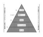
図2は、本出願の一実施形態による、コンピュータシステムのメモリの階層構造の概略図である。図2に示されたように、レジスタは上部に位置し、レベル0またはL0と表記される。レジスタの下位レベルのメモリはCPUキャッシュであり、キャッシュとも呼ばれる。複数のレベルのCPUキャッシュ、たとえば、レベル1、レベル2、および/またはレベル3が存在してよい。図2は、L1~L3と表記される3つのレベルのCPUキャッシュを示す。レジスタおよびCPUキャッシュは、一般に、各々SRAMを使用するが、レジスタのアクセスレートの方が通常高い。SRAMの典型的なアクセスレートは、数ナノ秒(nanosecond、ns)で測定される。CPUキャッシュの下位レベルのメモリは、L4と表記されるDRAMである。DRAMの典型的なアクセスレートは、数十ナノ秒で測定される。DRAMの下位レベルのメモリはフラッシュメモリである。フラッシュメモリの典型的なアクセスレートは、数十マイクロ秒(microsecond、μs)で測定される。フラッシュメモリの下位レベルのメモリレベルはディスクである。ディスクの典型的なアクセスレートは、数ミリ秒(millisecond、ms)で測定される。フラッシュメモリおよびディスクは、通常、コンピュータシステムのローカル大容量ストレージデバイスとして使用され、L5と記録される。現在のコンピュータシステムでは、ローカル大容量ストレージデバイスに加えて、リモート大容量ストレージデバイス、たとえば、クラウドストレージがさらに構成されてよい。図2から、コンピュータシステムのメモリの階層構造の上から下に、メモリの典型的なアクセスレートは降順であるが、単位容量当たりのコストは降順であることが容易に分かる。
FIG. 2 is a schematic diagram of the hierarchical structure of the memory of a computer system according to an embodiment of the present application. As shown in Figure 2, the registers are located at the top and are labeled level 0 or L0. The lower level memory of the register is the CPU cache, also known as the cache. There may be multiple levels of CPU cache, such as
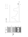
図3は、本出願の一実施形態による、コンピュータシステムのストレージサブシステムの概略構造図である。図3に示されたように、CPUキャッシュ3011およびレジスタファイル3012はCPU301に統合され、メインメモリ302は相互接続バス304を介してCPU301に接続され、I/Oデバイスとして使用される大容量ストレージデバイス(mass storage device)303は、I/Oインターフェース305および相互接続バス304を介してCPU301に接続される。
FIG. 3 is a schematic structural diagram of a storage subsystem of a computer system according to an embodiment of the present application. As shown in FIG. 3, the
メインメモリ(main memoryまたはprimary storage)は、略してMMである。メインメモリは、名前が意味するようにコンピュータシステム内の主メモリであり、CPUがプログラムを実行するときに必要な関連データおよびプログラム命令を一時的に格納するように構成される。メインメモリは、通常DRAMであり、レジスタまたはCPUキャッシュなどのSRAMを含むときもある。補助ストレージ(secondary storageまたはauxiliary storage)とも呼ばれる大容量ストレージデバイスは、一般に、フラッシュメモリまたは磁気ディスクを使用する。オペレーティングシステムおよびアプリケーションソフトウェアは、大容量ストレージデバイスに長期間格納することができる。しかしながら、大容量ストレージデバイスのアクセスレートはCPUのクロックサイクルと大きく異なるので、CPUによる直接アクセスに適していない。したがって、オペレーティングシステムまたはアプリケーションが実行される必要があるとき、関連データおよびプログラム命令は、大容量ストレージデバイスからメインメモリにコピーされる必要があり、メインメモリは、CPUによる高速アクセスのための要件を満たすために、CPUの実行に必要なデータおよび命令を一時的に格納する。 Main memory (main memory or primary storage) is abbreviated as MM. Main memory, as the name implies, is the main memory in a computer system and is configured to temporarily store relevant data and program instructions needed by the CPU to execute a program. The main memory is usually DRAM and may also contain SRAM such as registers or CPU cache. Large-capacity storage devices, also called secondary storage or auxiliary storage, generally use flash memory or magnetic disks. Operating system and application software can be stored for extended periods on large storage devices. However, since the access rate of the large-capacity storage device is significantly different from the clock cycle of the CPU, it is not suitable for direct access by the CPU. Therefore, when an operating system or application needs to be run, relevant data and program instructions need to be copied from the large storage device to main memory, which is a requirement for fast access by the CPU. Temporarily stores the data and instructions needed to run the CPU to meet.
メインメモリのパフォーマンスがコンピュータシステムのパフォーマンスを大きく左右することは明らかである。したがって、メインメモリはコンピュータシステムに不可欠な内部構成要素であり、内蔵メモリ(internal memoryまたはmemory)とも呼ばれる。それに対応して、大容量ストレージデバイスは、外部メモリ(external memory)とも呼ばれ、コンピュータシステムの外部に配置されてよい。しかしながら、大容量ストレージに対する需要は依然として増加しているので、現在、大容量ストレージデバイスは、コンピュータシステムの非常に重要な構成要素であり、通常、コンピュータシステムの内部に配置される。 It is clear that the performance of main memory has a great influence on the performance of computer systems. Therefore, main memory is an essential internal component of a computer system and is also referred to as internal memory or memory. Correspondingly, the mass storage device, also called external memory, may be located outside the computer system. However, as the demand for high-capacity storage is still increasing, high-capacity storage devices are now a very important component of computer systems and are usually located inside the computer system.
読取り速度が考慮されているが、メインメモリの総メモリ容量は、ワイヤレス通信デバイス全体のメモリ空間要件を満たすために、常により大きいことが期待される。しかしながら、現在、コストによって制限され、メインメモリの総メモリ容量は、大容量ストレージデバイスの記憶空間よりもかなり小さい。一例としてスマートフォンが使用される。スマートフォンの総メモリは、通常、数百メガバイト(megabyte、MB)から数ギガバイト(gigabyte、GB)の範囲、たとえば、512 MB、1GB、2GB、3GB、4GB、6GB、8GB、またはそれ以上である。大容量ストレージデバイスの記憶空間は、通常、数十GBから数百GBの範囲、たとえば、32GB、64B、128GB、256GB、512GB、またはそれ以上である。 Although read speed is taken into account, the total memory capacity of the main memory is always expected to be larger to meet the memory space requirements of the entire wireless communication device. However, currently limited by cost, the total memory capacity of main memory is significantly smaller than the storage space of large storage devices. A smartphone is used as an example. The total memory of a smartphone typically ranges from a few hundred megabytes (MB) to a few gigabytes (gigabyte, GB), for example 512 MB, 1GB, 2GB, 3GB, 4GB, 6GB, 8GB, or more. Storage space for high-capacity storage devices typically ranges from tens of GB to hundreds of GB, for example 32GB, 64B, 128GB, 256GB, 512GB, or more.
本出願のこの実施形態では、特に明記しない限り、メモリは、通常、コンピュータシステムのメインメモリであることを理解されたい。具体的には、メモリは、DDRメモリまたは略してDDRと呼ばれる、ダブルデータレート(double data rate、DDR)を備える同期式DRAM(synchronous DRAM、SDRAM)であってよい。一般的なSDRAMはクロックサイクルで1回だけデータを転送するが、DDR SDRAMはクロックサイクルで少なくとも2回データを転送することができ、したがって、データ転送速度はダブルデータレートと呼ばれる。DDRメモリには、電子素子技術連合評議会(Joint Electron Device Engineering Council、JEDEC)によって策定されたDDR1、DDR2、DDR3、およびDDR4、ならびにその後に進化した規格に基づくDDRメモリが含まれ、モバイルDDR(mobile DDR、MDDR)または低電力DDR(low power DDR、LPDDR、もしくはLP-DDR)と呼ばれるDDRメモリも含まれる。 It should be understood that in this embodiment of the present application, memory is usually the main memory of a computer system, unless otherwise stated. Specifically, the memory may be a DDR memory or a synchronous DRAM (synchronous DRAM, SDRAM) having a double data rate (DDR), which is abbreviated as DDR. While typical SDRAM transfers data only once in a clock cycle, DDR SDRAM can transfer data at least twice in a clock cycle, so the data transfer rate is called the double data rate. DDR memory includes DDR1, DDR2, DDR3, and DDR4 developed by the Joint Electron Device Engineering Council (JEDEC), as well as DDR memory based on later evolved standards, mobile DDR ( Also includes DDR memory called mobile DDR, MDDR) or low power DDR (low power DDR, LPDDR, or LP-DDR).
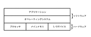
図4は、本出願の一実施形態による、コンピュータシステムの層状構造の概略図である。図4に示されたように、コンピュータシステムの階層構造では、ハードウェアは最下層に配置され、ソフトウェアは上位層に配置される。オペレーティングシステムは、コンピューティングデバイスのハードウェアリソースおよびソフトウェアリソースを管理するシステムソフトウェアであり、アプリケーションとハードウェアとの間のシステムソフトウェアと見なされてよい。オペレーティングシステムは、通常、メモリ管理(memory management)、I/Oデバイス管理、およびユーザ操作インターフェースなどの基本機能を提供することができる。ハードウェアに対する動作を実行するためにアプリケーションによって行われるいかなる試みも、オペレーティングシステムを使用して行われる必要がある。中間ソフトウェア、すなわち、オペレーティングシステムを導入すると、アプリケーションが複雑で多様な基盤となるハードウェアを使用するための簡単で一貫性があるメカニズムを提供することができ、基盤となるハードウェアが一部の制御不能なアプリケーションによって悪用されることを防止することもできる。 FIG. 4 is a schematic diagram of the layered structure of a computer system according to an embodiment of the present application. As shown in FIG. 4, in the hierarchical structure of a computer system, hardware is arranged at the bottom layer and software is arranged at the upper layer. An operating system is system software that manages the hardware and software resources of a computing device and may be considered system software between the application and the hardware. Operating systems can typically provide basic functions such as memory management, I / O device management, and user interaction interfaces. Any attempt made by the application to perform any action on the hardware must be made using the operating system. Introducing intermediate software, or operating system, can provide a simple and consistent mechanism for an application to use complex and diverse underlying hardware, with some underlying hardware. It can also be prevented from being abused by out-of-control applications.
加えて、コンピュータシステムによってサポートされる機能がより豊富になるにつれて、いくつかの重要な機能は、通常、比較的独立したサブシステムによって実装される。これらのサブシステムは、それぞれのオペレーティングシステムを有することができる。この場合、コンピュータシステムは複数のオペレーティングシステムを含んでよい。メインオペレーティングシステムは、コンピュータシステムのメインシステム内で実行されて、コンピュータシステムのソフトウェアリソースおよびハードウェアリソースを管理する。加えて、補助オペレーティングシステムは、サブシステム内で実行されて、サブシステムのソフトウェアリソースおよびハードウェアリソースを管理することができる。 In addition, as more and more features are supported by computer systems, some important features are usually implemented by relatively independent subsystems. These subsystems can have their own operating system. In this case, the computer system may include multiple operating systems. The main operating system runs within the main system of the computer system and manages the software and hardware resources of the computer system. In addition, the auxiliary operating system can run within the subsystem to manage the software and hardware resources of the subsystem.
一例として携帯電話が使用される。現在、携帯電話プラットフォームのメインオペレーティングシステムは、通常、アンドロイド(登録商標)オペレーティングシステムまたはアイフォンオペレーティングシステムである。メインオペレーティングシステムは、携帯電話全体のソフトウェアリソースおよびハードウェアリソースを管理し、ユーザにグラフィック操作インターフェースを提供することができる。加えて、進化し続ける無線アクセス技術(radio access technology、RAT)をサポートするために、通常、携帯電話内部に適切に設計された通信サブシステムが存在する。メインオペレーティングシステムとは異なるオペレーティングシステムが通信サブシステム内で実行されてよい。通信サブシステム内で実行されるオペレーティングシステムは、本出願のこの実施形態では、通信オペレーティングシステムと表記される。通信オペレーティングシステムは、通常、リアルタイムオペレーティングシステム(real time operating system、RTOS)である。しかしながら、アンドロイド(登録商標)オペレーティングシステムおよびアイフォンオペレーティングシステムなどの携帯電話プラットフォームのオペレーティングシステムは、リアルタイムオペレーティングシステムと見なされない。オペレーティングシステムの理論によれば、「リアルタイム」は、通常、特定の動作、たとえばメモリ割当て動作に費やされる時間が、オペレーティングシステムによって約束された上限時間を超えないことを意味する。したがって、通信サブシステムがリアルタイムオペレーティングシステムを使用すると、いくつかのワイヤレス通信サービスの低遅延要件をよりよく満たすのに役立つ。 A mobile phone is used as an example. Currently, the main operating system of mobile phone platforms is usually the Android® operating system or the iPhone operating system. The main operating system can manage the software and hardware resources of the entire mobile phone and provide the user with a graphic operation interface. In addition, there are usually well-designed communication subsystems inside mobile phones to support the ever-evolving radio access technology (RAT). An operating system different from the main operating system may be running within the communication subsystem. An operating system running within a communications subsystem is referred to as a communications operating system in this embodiment of the present application. The communication operating system is usually a real time operating system (RTOS). However, mobile phone platform operating systems such as the Android® operating system and the iPhone operating system are not considered real-time operating systems. According to operating system theory, "real time" usually means that the time spent on a particular operation, eg, a memory allocation operation, does not exceed the time limit promised by the operating system. Therefore, the use of real-time operating systems by communication subsystems helps to better meet the low latency requirements of some wireless communication services.
コンピュータシステムのアプリケーションとサブシステムの両方を実行するプロセスでは、メモリ空間の一部が使用される必要がある。コンピュータシステムのアプリケーションまたはサブシステムが実行されているとき、オペレーティングシステムは、通常、メモリ空間の一部をアプリケーションまたはサブシステムに割り当てる。オペレーティングシステムの場合、メモリ管理は動的メモリ管理および静的メモリ管理に分類されてよい。動的メモリ管理のソリューションでは、オペレーティングシステムによってアプリケーションまたはサブシステムに割り当てられたメモリ空間のこの部分は、動的メモリ空間または動的メモリと呼ばれる場合がある。アプリケーションまたはサブシステムによって使用されていないとき、動的メモリ空間は、別のアプリケーションまたはサブシステムが使用するためにオペレーティングシステムによって再割当てされてよい。静的メモリ管理のソリューションでは、オペレーティングシステムによってアプリケーションまたはサブシステムに割り当てられたメモリ空間のこの部分は、静的メモリ空間または静的メモリと呼ばれる場合がある。静的メモリ空間がアプリケーションまたはサブシステムによって使用されていない場合でも、静的メモリ空間は、別のサブシステムまたはアプリケーションが使用することはできない。 A part of memory space needs to be used in the process of running both applications and subsystems of a computer system. When an application or subsystem of a computer system is running, the operating system typically allocates a portion of memory space to the application or subsystem. For operating systems, memory management may be categorized as dynamic memory management and static memory management. In dynamic memory management solutions, this portion of the memory space allocated to an application or subsystem by the operating system may be referred to as dynamic memory space or dynamic memory. When not used by an application or subsystem, the dynamic memory space may be reallocated by the operating system for use by another application or subsystem. In static memory management solutions, this portion of the memory space allocated to an application or subsystem by the operating system may be referred to as static memory space or static memory. A static memory space cannot be used by another subsystem or application, even if the static memory space is not used by the application or subsystem.
コンピュータシステムの継続的な進化に伴い、コンピュータシステム用のより多くのサブシステムが存在し、これらのサブシステムはますます高いメモリ要件を課している。以下では、一例としてワイヤレス通信デバイスの通信サブシステムを使用して、本出願のこの実施形態において提供されるいくつかのメモリ管理ソリューションを詳細に記載する。これらのメモリ管理方式は、コンピュータシステムのサブシステムのメモリ要件をよりよく満たすのに役立つ。たとえば、本出願のいくつかのオプションの実施形態において提供されるメモリ管理ソリューションは、メモリ割当て遅延を低減し、特に厳しい遅延要件を有するサブシステムのメモリ要件を満たすのに役立つことができる。本出願の他のオプションの実施形態において提供されるメモリ管理ソリューションでは、より多くの利用可能なメモリを提供することができ、それにより、メモリコストの削減またはメモリ使用効率の改善に役立つ。通信サブシステムはコンピュータのサブシステムの単なる例であり、本出願のこの実施形態において提供されるソリューションは、コンピュータの別のサブシステムにも適用可能であることを理解されたい。 With the continued evolution of computer systems, there are more subsystems for computer systems, and these subsystems impose increasingly higher memory requirements. The following describes in detail some memory management solutions provided in this embodiment of the present application, using the communication subsystem of a wireless communication device as an example. These memory management schemes help better meet the memory requirements of the subsystems of a computer system. For example, the memory management solutions provided in some optional embodiments of the present application can help reduce memory allocation delays and meet the memory requirements of subsystems with particularly stringent delay requirements. The memory management solutions provided in embodiments of other options of the present application can provide more available memory, thereby helping to reduce memory costs or improve memory usage efficiency. It should be understood that the communication subsystem is merely an example of a computer subsystem and that the solutions provided in this embodiment of the present application are applicable to other computer subsystems.
図5は、本出願の一実施形態による、ワイヤレス通信デバイスの概略構造図である。 FIG. 5 is a schematic structural diagram of a wireless communication device according to an embodiment of the present application.
本出願のこの実施形態では、ワイヤレス通信デバイスは、ワイヤレス通信機能を有するコンピューティングデバイスであることを理解されたい。ワイヤレス通信シデバイスは、ワイヤレス通信システム内の端末であってもよく、基地局などの無線アクセスネットワークデバイスであってもよい。図5に示された端末および基地局は、第3世代パートナーシッププロジェクト(3rd Generation Partnership Project、3GPP)技術仕様に基づく移動通信システムの一例として使用され得るか、または他のワイヤレス通信規格、たとえば、ワイヤレス通信規格802.11、802.15、および802.20などの電気電子技術者協会(Institute of Electrical and Electronics Engineers、IEEE)の802シリーズに基づくワイヤレス通信システムを包含することができる。 It should be understood that in this embodiment of the present application, the wireless communication device is a computing device having a wireless communication function. The wireless communication system may be a terminal in a wireless communication system or a wireless access network device such as a base station. The terminals and base stations shown in Figure 5 can be used as an example of a mobile communication system based on the 3rd Generation Partnership Project (3GPP) technical specifications, or other wireless communication standards, such as wireless. It can include wireless communication systems based on the Institute of Electrical and Electronics Engineers (IEEE) 802 series, such as communication standards 802.11, 802.11, and 802.11.
端末は、ユーザ機器(user equipment、UE)、移動局(mobile station、MS)、または加入者ユニット(subscriber unit、SU)と呼ばれる場合もある。端末は、携帯電話、タブレットコンピュータ(tablet computer)、ラップトップコンピュータ(laptop computer)、ウェアラブルデバイス(たとえば、スマートウォッチ、スマートバンド、スマートヘルメット、もしくはスマートグラス)、またはスマートホームデバイス(たとえば、スマートメータもしくはスマートアプライアンス)、スマートビークルなどを含む、任意のモノのインターネットデバイスなどの、ワイヤレスアクセス機能を有する別の通信デバイスであってよいが、それらに限定されない。基地局は、具体的には、第5世代(5th Generation、5G)移動通信システムにおける汎用ノードB(generation Node B、gNB)、第4世代(4th Generation、4G)移動通信システムにおける発展型ノードB(evolutional Node B、eNBもしくはeNodeB)、または別の可能な無線アクセス技術における基地局であってよい。複数の物理形態および送信電力の基地局、たとえば、マクロ基地局(macro base station)またはマイクロ基地局(micro base station)が存在してもよい。 The terminal may also be referred to as a user equipment (UE), mobile station (MS), or subscriber unit (SU). The terminal can be a mobile phone, tablet computer, laptop computer, wearable device (eg, smartwatch, smartband, smart helmet, or smartglass), or smart home device (eg, smart meter or). It may be, but is not limited to, another communication device with wireless access capabilities, such as, but not limited to, smart appliances), smart vehicles, and other Internet of Things devices. Specifically, the base station is an advanced type in the general-purpose node B (generation Node B, gNB ) in the 5th generation (5G) mobile communication system and the 4th generation (4th Generation, 4G ) mobile communication system. It may be node B (evolutional Node B, eNB or eNodeB), or a base station in another possible radio access technology. There may be multiple physical form and transmit power base stations, such as macro base stations or micro base stations.
図5に示されたように、ワイヤレス通信デバイスは、アプリケーションサブシステム501、メモリ(memory)502、および通信サブシステム503を含む。アプリケーションサブシステム501および通信サブシステム503は、相互接続バスを介してメモリ502に接続され、アプリケーションサブシステム501と通信サブシステム503の両方は、メモリ502によって提供されるメモリ空間を使用することができる。アプリケーションサブシステム501は、ワイヤレス通信デバイスの主制御システムまたは主計算システムとして使用されてよく、メインオペレーティングシステムおよびアプリケーションを実行し、ワイヤレス通信デバイス全体のソフトウェアリソースおよびハードウェアリソースを管理し、ユーザにユーザ操作インターフェースを提供するように構成される。通信サブシステム503は、通信オペレーティングシステムおよび通信機能ソフトウェアを実行し、通信サブシステムのソフトウェアリソースおよびハードウェアリソースを管理し、ユーザにワイヤレス通信機能を提供するように構成される。
As shown in FIG. 5, wireless communication devices include
アプリケーションサブシステム501は、1つまたは複数の処理コア(core)を含んでよい。図5は、コア1(C-1)、コア2(C-2)、コア3(C-3)、およびコアn(C-n)を含むマルチコアアプリケーションサブシステムを示し、ここで、nは正の整数である。本明細書では、nは単なる例である。nの値は、4未満、たとえば、2または1であってもよく、4以上、たとえば、4、8、10、または12であってもよい。異なるコアの機能は異なっていてよく、たとえば、優位周波数が異なる。各コアは対応する専用キャッシュを含んでよく、複数のコアの間に共有キャッシュが存在してよい。加えて、アプリケーションサブシステム501は、別のサブシステムに関連するドライブソフトウェアを含んでよい。
The
通信サブシステム503は、無線周波数(radio frequency、RF)サブシステムおよびベースバンド(baseband、BB)サブシステムにさらに分割されてよい。無線周波数サブシステムは、主に無線周波数信号を処理するように構成され、図5ではRFモジュールによって表されている。具体的には、無線周波数サブシステムは、受信経路(receive path)および送信経路(transmit path)を提供するために、アンテナ、スイッチ、低雑音増幅器、電力増幅器、ミキサ、発振器、フィルタ、およびプロセッサなどの電子デバイスを含んでよい。受信経路は、アンテナを介して無線周波数信号を受信し、無線周波数信号に対して処理(たとえば、増幅、フィルタリング、およびダウンコンバージョン)を実行して、中間周波数信号またはベースバンド信号を取得し、中間周波数信号またはベースバンド信号をベースバンドサブシステムに転送するように構成される。受信経路は、ベースバンドサブシステムから中間周波数信号またはベースバンド信号を受信し、中間周波数信号またはベースバンド信号に対して処理(たとえば、アップコンバージョン、増幅、およびフィルタリング)を実行して、無線周波数を取得し、最後にアンテナを介して無線周波数信号を空間に放射するように構成される。
The
ベースバンドサブシステムは、1つまたは複数の処理コア、アナログデジタル変換構成要素、ベースバンドプロセッサ(baseband processor、BBP)、ハードウェアアクセラレータ(hardware accelerator、HAC)、キャッシュなどを含んでよい。説明の目的で、ベースバンドプロセッサ、処理コア、ハードウェアアクセラレータ、およびキャッシュが図5に示されている。これらの電子部品のタイプおよび数は、本出願のこの実施形態では限定されないことを理解されたい。ベースバンドサブシステムは、図5に示されたいくつかの構成要素(たとえば、HAC)を含まなくてもよく、図5に示されていないいくつかの構成要素(たとえば、アナログデジタル変換構成要素)を含んでもよい。アナログデジタル変換構成要素には、アナログ信号をデジタル文字に変換するアナログデジタルコンバータ(analog to digital converter、ADC)、およびデジタル信号をアナログ信号に変換するデジタルアナログコンバータ(digital to analog converter、DAC)が含まれる。 The baseband subsystem may include one or more processing cores, analog-digital conversion components, baseband processor (BBP), hardware accelerator (HAC), cache, and the like. For illustration purposes, the baseband processor, processing core, hardware accelerator, and cache are shown in Figure 5. It should be understood that the types and numbers of these electronic components are not limited in this embodiment of the present application. The baseband subsystem may not include some components shown in FIG. 5 (eg HAC) and may not include some components not shown in FIG. 5 (eg analog-to-digital conversion components). May include. Analog-to-digital conversion components include analog-to-digital converters (ADCs) that convert analog signals to digital characters, and digital-to-analog converters (DACs) that convert digital signals to analog signals. Is done.
ベースバンドプロセッサは、基地局から発信されたデジタル信号から有用な情報もしくはデータビットを抽出するか、またはアプリケーションサブシステムから発信された情報もしくはデータビットを基地局に送信されるデジタル信号に変換するように構成されてよい。情報またはデータビットは、音声、テキスト、またはビデオなどのユーザデータまたは制御情報を表すデータであってよい。具体的には、ベースバンドプロセッサは、変調、復調、符号化、および復号などのベースバンド信号処理動作を実施することができる。加えて、異なる無線アクセス技術、たとえば、5Gの新無線(new radio、NR)および4Gのロングタームエボリューション(long term evolution、LTE)、まったく同じではないベースバンド信号処理動作が実行されてよい。したがって、複数の移動通信モードの併合をサポートするために、複数の処理コア、および複数のベースバンドプロセッサさえ同時に含まれてよい。 The baseband processor should extract useful information or data bits from the digital signal transmitted from the base station or convert the information or data bits transmitted from the application subsystem into a digital signal transmitted to the base station. May be configured in. The information or data bit may be data representing user data or control information such as voice, text, or video. Specifically, the baseband processor can perform baseband signal processing operations such as modulation, demodulation, coding, and decoding. In addition, different radio access technologies such as 5G new radio (NR) and 4G long term evolution (LTE), baseband signal processing operations that are not exactly the same may be performed. Therefore, a plurality of processing cores and even a plurality of baseband processors may be included at the same time to support the merging of a plurality of mobile communication modes.
ハードウェアアクセラレータは、処理のオーバーヘッドが比較的高いいくつかのサブ機能、たとえば、データパケット(data packet)の組立、構文解析、暗号化、および解読を実施するように構成されてよい。これらのサブ機能は、共通機能を有するプロセッサを使用して実施されてもよい。しかしながら、パフォーマンスまたはコストを考慮すると、ハードウェアアクセラレータを使用してこれらのサブ機能を実施する方が適切な場合がある。したがって、ハードウェアアクセラレータのタイプおよび数は、要件に基づいて具体的に選択されてよい。特定の実装形態では、フィールドプログラマブルゲートアレイ(field programmable gate array、FPGA)および特定用途向け集積回路(application specified integrated circuit、ASIC)のうちの1つまたは組合せが実施に使用されてよい。確かに、1つまたは複数の処理コアがハードウェアアクセラレータ内で使用されてもよい。 The hardware accelerator may be configured to perform some sub-features with relatively high processing overhead, such as data packet assembly, parsing, encryption, and decryption. These sub-functions may be performed using a processor having a common function. However, performance or cost considerations may make it more appropriate to use hardware accelerators to perform these sub-features. Therefore, the type and number of hardware accelerators may be specifically selected based on the requirements. In a particular implementation, one or a combination of a field programmable gate array (FPGA) and an application specified integrated circuit (ASIC) may be used in the implementation. Indeed, one or more processing cores may be used within the hardware accelerator.
本出願のこの実施形態では、ワイヤレス通信デバイスの各処理コアは1つのプロセッサを表すことができ、プロセッサは、汎用プロセッサであってもよく、特定の分野のために設計されたプロセッサであってもよいことを理解されたい。たとえば、プロセッサは、CPUであってもよく、デジタル信号プロセッサ(digital signal processor、DSP)であってもよい。必要に応じて、プロセッサは、マイクロ制御装置(micro control unit、MCU)、グラフィックス処理装置(graphics processing unit、GPU)、画像信号プロセッサ(image signal processing、ISP)、オーディオ信号プロセッサ(audio signal processor、ASP)、または人工知能(artificial intelligence、AI)アプリケーションに適用され、ニューラルネットワーク処理装置(neural network processing unit、NPU)、テンソル処理装置(tensor processing unit、TPU)、もしくはAIエンジンと呼ばれるプロセッサを含むが、それらに限定されない任意のプロセッサであってよい。 In this embodiment of the present application, each processing core of a wireless communication device can represent one processor, which may be a general purpose processor or a processor designed for a particular field. Please understand that it is good. For example, the processor may be a CPU or a digital signal processor (DSP). If necessary, the processor includes a micro control unit (MCU), a graphics processing unit (GPU), an image signal processing (ISP), and an audio signal processor (audio signal processor,). Applies to ASPs, or artificial intelligence (AI) applications, including processors called neural network processing units (NPUs), tensor processing units (TPUs), or AI engines. , Any processor, not limited to them.
実際のアプリケーションでは、アプリケーションシナリオの要件に基づいて、ワイヤレス通信デバイスは、異なる数の処理コアと異なるタイプの処理コアの組合せを使用することができる。加えて、通信サブシステム503における無線周波数サブシステムおよびベースバンドサブシステムの機能分割も調整されてよい。たとえば、無線周波数サブシステムの一部の機能がベースバンドサブシステムに統合されるか、またはベースバンドサブシステムの一部の機能が無線周波数サブシステムに統合される。
In real-world applications, wireless communication devices can use different numbers of processing cores and different types of processing core combinations, based on the requirements of the application scenario. In addition, the functional division of the radio frequency and baseband subsystems in the
一実装形態では、無線周波数サブシステムは、独立したアンテナ、独立した無線周波数フロントエンド(RF front end、RFFE)デバイス、および独立した無線周波数処理チップを含んでよい。無線周波数処理チップは、受信機(receiver)、送信機(transmitter)、またはトランシーバ(transceiver)と呼ばれることもある。アンテナ、無線周波数フロントエンドデバイス、および無線周波数処理チップのすべては、個別に製造および販売することができる。確かに、無線周波数サブシステムは、電力消費およびパフォーマンスに対する要件に基づいて、異なる構成要素または異なる統合方式を使用することもできる。たとえば、無線周波数フロントエンドデバイスに属するいくつかの構成要素は、無線周波数処理チップに統合される。 In one implementation, the radio frequency subsystem may include a separate antenna, a separate radio frequency front end (RFFE) device, and a separate radio frequency processing chip. The radio frequency processing chip may also be referred to as a receiver, transmitter, or transceiver. Antennas, radio frequency front-end devices, and radio frequency processing chips can all be manufactured and sold separately. Indeed, radio frequency subsystems can also use different components or different integration schemes based on power consumption and performance requirements. For example, some components belonging to a radio frequency frontend device are integrated into a radio frequency processing chip.
一実装形態では、ベースバンドサブシステムは独立したチップとして使用される場合があり、チップはモデム(modem)と呼ばれる場合がある。ベースバンドサブシステムのハードウェア構成要素は、modemによって製造および販売されてよい。ベースバンドプロセッサはワイヤレス通信用のコアデバイスなので、モデム(modem)はベースバンドチップまたはベースバンドプロセッサと呼ばれることもある。別の実装形態では、ベースバンドサブシステムはさらにSoCチップに統合される場合があり、SoCチップによって製造および販売される。加えて、ベースバンドサブシステムのソフトウェア構成要素は、納入前にハードウェア構成要素内で構築されてもよく、納入後に他の不揮発性メモリからハードウェア構成要素にインポートされてもよく、これらのソフトウェア構成要素がネットワークを介してオンラインで更新およびアップグレードされてもよい。 In one implementation, the baseband subsystem may be used as an independent chip, which may be referred to as a modem. The hardware components of the baseband subsystem may be manufactured and sold by modem. Since the baseband processor is a core device for wireless communication, the modem is sometimes referred to as the baseband chip or baseband processor. In another implementation, the baseband subsystem may be further integrated into the SoC chip, manufactured and sold by the SoC chip. In addition, the baseband subsystem software components may be built within the hardware components prior to delivery or may be imported from other non-volatile memory into the hardware components after delivery, such software. Components may be updated and upgraded online over the network.
通信サブシステムを実行するプロセスでは、大量のデータ処理動作が実行される場合がある。その結果、特定のメモリ空間が占有される。加えて、ワイヤレス通信サービスは、低遅延に対する比較的高い要件を有する。したがって、ワイヤレス通信デバイスのメインオペレーティングシステムが通信サブシステムに動的にメモリを割り当てる場合、メモリ割当て遅延は比較的長い可能性があり、その結果、低遅延に対する一部のワイヤレス通信サービスの要件を満たすことができない。したがって、低遅延に対するワイヤレス通信サービスの要件を満たすために、メモリ空間の一部が通信サブシステムに固定的に割り当てられてよく、通信オペレーティングシステムによって直接管理される。 A large amount of data processing operations may be performed in the process of executing the communication subsystem. As a result, a specific memory space is occupied. In addition, wireless communication services have relatively high requirements for low latency. Therefore, if the main operating system of the wireless communication device dynamically allocates memory to the communication subsystem, the memory allocation delay can be relatively long and, as a result, meet the requirements of some wireless communication services for low latency. Can't. Therefore, in order to meet the requirements of wireless communication services for low latency, a portion of the memory space may be fixedly allocated to the communication subsystem and managed directly by the communication operating system.
図6は、本出願の一実施形態による、ワイヤレス通信デバイスのメモリ割当ての概略図である。 FIG. 6 is a schematic diagram of memory allocation of a wireless communication device according to an embodiment of the present application.
図6の左側に示されたように、ワイヤレス通信デバイスの総メモリ容量は、上から下に「その他」、「アプリケーションサブシステム」、および「通信サブシステム」と表記された3つの部分に固定的に分割される。「その他」は、メモリ空間のこの部分が他の目的で使用されている、たとえば、他のサブシステム用に確保されていることを示す。「アプリケーションサブシステム」は、メモリ空間のこの部分が、アプリケーションサブシステムが使用するために割り当てられていることを示し、A1と表記される。最大のメモリ空間は、通常、アプリケーションサブシステムに割り当てられる。メモリ空間のこの部分は、アプリケーションサブシステム内で実行されるメインオペレーティングシステムによって直接管理され、必要に応じて、ワイヤレス通信デバイス内で実行されるアプリケーションおよび一部のサブシステムが使用するために割り当てられている。図6に示されたメモリ分割は単なる例であることを理解されたい。ワイヤレス通信デバイスのメモリは、別の方式で分割されてよく、たとえば、メモリが2つの部分、4つの部分、またはそれ以上の部分に分割される。 As shown on the left side of Figure 6, the total memory capacity of a wireless communication device is fixed in three parts, labeled "Other", "Application Subsystem", and "Communication Subsystem" from top to bottom. It is divided into. "Other" indicates that this portion of memory space is being used for other purposes, for example reserved for other subsystems. "Application subsystem" indicates that this portion of memory space is allocated for use by the application subsystem and is referred to as A1. The largest memory space is typically allocated to the application subsystem. This portion of memory space is managed directly by the main operating system running within the application subsystem and is allocated for use by applications running within the wireless communication device and some subsystems as needed. ing. It should be understood that the memory partitioning shown in Figure 6 is just an example. The memory of a wireless communication device may be divided in another way, for example, the memory is divided into two parts, four parts, or more.
「通信サブシステム」は、メモリ空間のこの部分が、通信サブシステムが使用するために割り当てられていることを示し、C1と表記される。通信サブシステムに割り当てられたメモリ空間のこの部分は、通常、通信オペレーティングシステムによって直接管理され、通常、メインオペレーティングシステムからは見えない。言い換えれば、通信サブシステムが割り当てられたメモリ空間のすべてを使用しない場合でも、メモリ空間は、メインオペレーティングシステムによって別のサブシステムまたはアプリケーションが使用するために割り当てることはできない。したがって、この意味で、通信サブシステムに固定的に割り当てられたメモリ空間のこの部分はまた、メインオペレーティングシステム用の静的メモリ空間と同等である。 "Communication subsystem" indicates that this portion of memory space is allocated for use by the communication subsystem and is referred to as C1. This portion of the memory space allocated to the communication subsystem is usually managed directly by the communication operating system and is usually invisible to the main operating system. In other words, a memory space cannot be allocated for use by another subsystem or application by the main operating system, even if the communication subsystem does not use all of the allocated memory space. Therefore, in this sense, this portion of the memory space fixedly allocated to the communication subsystem is also equivalent to the static memory space for the main operating system.
加えて、ワイヤレス通信サービスのパフォーマンスを保証するために、通信サブシステムに割り当てられるメモリ空間のサイズは、通常、ワイヤレス通信で使用されるピークレートを参照して決定される。しかしながら、ワイヤレス通信デバイスの動作サイクル内で、ワイヤレス通信で使用されるピークレートの時間比率は、通常、比較的小さい。この場合、通信サブシステムに割り当てられたメモリ空間の実際の使用量が多くない可能性があり、これにより、統計的な意味でメモリ空間の浪費が発生する可能性がある。 In addition, to ensure the performance of wireless communication services, the size of the memory space allocated to the communication subsystem is typically determined with reference to the peak rate used for wireless communication. However, within the operating cycle of a wireless communication device, the time ratio of the peak rate used for wireless communication is usually relatively small. In this case, the actual usage of memory space allocated to the communication subsystem may not be high, which may result in wasted memory space in a statistical sense.
統計的な意味でメモリ空間を浪費する現象が図6の右側に示されている。実線は通信サブシステムに割り当てられたメモリ容量を表し、C1と表記される。破線は通信サブシステムによって実際に使用されるメモリ容量を表し、C2と表記される。図6から、時点t1とt2との間で、通信サブシステムによって実際に使用されるメモリ容量C2は、通信サブシステムに固定的に割り当てられたメモリ容量C1よりも常に小さく、C1とC2との間の差は十分に使用されていないメモリ容量を表すことが分かる。加えて、統計的な意味では、メモリ空間の浪費度は、通信サブシステムに固定的に割り当てられたメモリ空間のサイズに正比例する。 The phenomenon of wasting memory space in a statistical sense is shown on the right side of FIG. The solid line represents the memory capacity allocated to the communication subsystem and is written as C1. The dashed line represents the amount of memory actually used by the communication subsystem and is referred to as C2. From FIG. 6, between time points t1 and t2, the memory capacity C2 actually used by the communication subsystem is always smaller than the memory capacity C1 fixedly allocated to the communication subsystem, with C1 and C2. It can be seen that the difference between them represents an underutilized memory capacity. In addition, in a statistical sense, the amount of memory space wasted is directly proportional to the size of the memory space that is fixedly allocated to the communication subsystem.
一例として携帯電話が使用される。4Gネットワークのピークモバイルデータレートは、1.2ギガビット/秒(Gigabit per second、Gbps)に達する可能性がある。モバイルデータを格納するために、少なくとも150MBのメモリ空間が必要である。4Gネットワークをサポートする携帯電話の場合、150MBのメモリ空間を4G通信サブシステムに固定的に割り当てることは大きい問題ではないかもしれない。しかしながら、5Gネットワークのピークモバイルデータレートは10Gbpsに達する可能性があり、それだけのモバイルデータを格納するために、少なくとも1.25GBのメモリ空間が必要である。この場合、1.25GBのメモリ空間が5G通信サブシステムに固定的に割り当てられた場合、携帯電話のメモリ容量に対する要件が大幅に増大し、その結果、メモリコストが増加する。 A mobile phone is used as an example. Peak mobile data rates for 4G networks can reach 1.2 gigabits per second (Gbps). At least 150MB of memory space is required to store mobile data. For mobile phones that support 4G networks, a fixed allocation of 150MB of memory space to the 4G communication subsystem may not be a major issue. However, the peak mobile data rate of 5G networks can reach 10 Gbps, requiring at least 1.25 GB of memory space to store that much mobile data. In this case, if 1.25 GB of memory space is fixedly allocated to the 5G communication subsystem, the requirement for the memory capacity of the mobile phone will increase significantly, resulting in an increase in memory cost.
加えて、通信サブシステムが(音声、ビデオ、およびテキストなどの)大量のアプリケーションデータを受信するとき、通信サブシステムは、アプリケーションデータをアプリケーションサブシステムに転送する必要がある。メモリの観点から、通信サブシステムに対応するメモリ空間のこの部分に一時的に格納されたアプリケーションデータは、アプリケーションサブシステムに対応するメモリ空間の部分に転送またはコピーされる必要がある。これらの転送またはコピー動作により、大量のメモリアクセスオーバーヘッドが発生し、システムの電力消費が増加し、サービス遅延が増加する。場合によっては、送信される必要があるアプリケーションデータの量が多すぎると、大量のメモリアクセスオーバーヘッドが最大メモリアクセス帯域幅を超えて、ワイヤレス通信サービスの障害が発生する可能性がある。 In addition, when the communication subsystem receives a large amount of application data (such as voice, video, and text), the communication subsystem needs to transfer the application data to the application subsystem. From a memory perspective, application data temporarily stored in this portion of the memory space corresponding to the communication subsystem needs to be transferred or copied to the portion of the memory space corresponding to the application subsystem. These transfer or copy operations incur a large amount of memory access overhead, increase system power consumption, and increase service delays. In some cases, too much application data needs to be sent, which can cause a large amount of memory access overhead to exceed the maximum memory access bandwidth and cause wireless communication service failures.
図7は、本出願の一実施形態による、別のワイヤレス通信デバイスの概略構造図である。図5に示されたワイヤレス通信デバイスに基づいて、メモリ管理アクセラレータ(memory management accelerator、MMA)がワイヤレス通信デバイス上に示されている。メモリ管理アクセラレータは、通信サブシステムにメモリ管理動作を提供するように構成され、オペレーティングシステム(通信オペレーティングシステムまたはメインオペレーティングシステム)のメモリ管理機能を部分的に置き換えることができる。 FIG. 7 is a schematic structural diagram of another wireless communication device according to an embodiment of the present application. Based on the wireless communication device shown in Figure 5, a memory management accelerator (MMA) is shown on the wireless communication device. Memory management accelerators are configured to provide memory management operations to communication subsystems and can partially replace the memory management capabilities of the operating system (communication operating system or main operating system).
図7に示されたように、ワイヤレス通信デバイスは、相互接続バスを介して接続されたアプリケーションサブシステム701、メモリ702、通信サブシステム703、およびメモリ管理アクセラレータ704を含む。アプリケーションサブシステム701は、メインオペレーティングシステムを実行し、ワイヤレス通信デバイスのソフトウェアリソースおよびハードウェアリソースを管理し、詳細には、アプリケーションサブシステムのメモリ空間を管理するように構成されてよい。通信サブシステムは、通信オペレーティングシステムおよび通信機能ソフトウェアを実行し、通信サブシステムのソフトウェアリソースおよびハードウェアリソースを管理し、詳細には、通信サブシステムのメモリ空間を管理することができる。図7では、アプリケーションサブシステム701の処理コアはACoreと表記され、通信サブシステム703の処理コアはCCoreと表記されている。図7のアプリケーションサブシステム701、メモリ702、ならびに(RFモジュール、HAC、およびBBPを含む)通信サブシステム703は、それぞれ、図5に示されたアプリケーションサブシステム501、メモリ502、および通信サブシステム503に対応することを理解されたい。関連する詳細については、前述の説明を参照されたい。繰り返される内容は再び記載されない。
As shown in FIG. 7, the wireless communication device includes an
本出願のこの実施形態では、メモリ管理アクセラレータはハードウェアアクセラレータであり、ハードウェアアクセラレータはハードウェア構成要素を含むが、ソフトウェア構成要素も含んでよい。ハードウェア構成要素およびソフトウェア構成要素は、メモリ管理アクセラレータと呼ばれるか、または略してMMAサブシステムであるメモリ管理アクセラレータサブシステムを一緒に形成することができる。メモリ管理アクセラレータのハードウェア構成要素は、計算に使用される処理構成要素、たとえば、ASIC、FPGA、または処理コアのうちの1つまたは複数を含む。メモリ管理アクセラレータのハードウェア構成要素は、メモリ、たとえば、レジスタ、キャッシュ、または密結合メモリ(tightly coupled memory、TCM)をさらに含んでよい。メモリ管理アクセラレータのソフトウェア構成要素は、メモリ管理アクセラレータのハードウェア構成要素に適合し、ハードウェア構成要素と連携して、通信サブシステムにメモリ管理動作を一緒に提供するように構成されてよい。 In this embodiment of the present application, the memory management accelerator is a hardware accelerator, and the hardware accelerator includes a hardware component, but may also include a software component. Hardware and software components can be referred to as memory management accelerators, or together they can form a memory management accelerator subsystem, which is an MMA subsystem for short. The hardware components of a memory management accelerator include one or more of the processing components used in the computation, such as an ASIC, FPGA, or processing core. Hardware components of memory management accelerators may further include memory, such as registers, caches, or tightly coupled memory (TCM). The software component of the memory management accelerator may be configured to adapt to the hardware component of the memory management accelerator and to work with the hardware component to provide memory management operations to the communication subsystem together.
したがって、本出願のこの実施形態では、メモリ管理アクセラレータは、独立したハードウェア構成要素であってもよく、ハードウェア構成要素とソフトウェア構成要素の組合せであってもよい。加えて、メモリ管理アクセラレータのハードウェア構成要素は、ワイヤレス通信デバイス内の元の構成要素の処理圧力を増大させることなく、ワイヤレス通信デバイスに新しく追加されたハードウェア構成要素であってよい。あるいは、ワイヤレス通信デバイスの元のハードウェア構成要素は、メモリ管理アクセラレータのハードウェア構成要素として再利用されてよく、ソフトウェア構成要素は、本出願のこの実施形態において提供されるメモリ管理アクセラレータの機能を実装するようにアップグレードされる。メモリ管理アクセラレータは、独立したICチップであってもよく、通信チップまたはSoCチップに統合されてもよい。 Therefore, in this embodiment of the present application, the memory management accelerator may be an independent hardware component or a combination of hardware and software components. In addition, the hardware component of the memory management accelerator may be a newly added hardware component to the wireless communication device without increasing the processing pressure of the original component within the wireless communication device. Alternatively, the original hardware component of the wireless communication device may be reused as the hardware component of the memory management accelerator, which software component provides the functionality of the memory management accelerator provided in this embodiment of the present application. Upgraded to implement. The memory management accelerator may be an independent IC chip or may be integrated into a communication chip or an SoC chip.
メモリ管理アクセラレータは、別の名前、たとえば、メモリ管理ハードウェアアクセラレータ(memory management hardware accelerator、MMHAまたはMMHAC)、メモリアクセラレータ(memory accelerator、MA)、メモリハードウェアアクセラレータ(memory hardware accelerator、MHAまたはMHAC)、メモリ加速エンジン(memory acceleration engine、MAE)、メモリ割当てアクセラレータ(memory allocation accelerator、MAA)、メモリ割当てハードウェアアクセラレータ(memory allocation hardware accelerator、MAHAまたはMAHAC)、メモリアクセスアクセラレータ(memory access accelerator、MAA)、メモリアクセスハードウェアアクセラレータ(memory access hardware accelerator、MAHAまたはMAHAC)などを有してもよい。 Memory management accelerators have different names, such as memory management hardware accelerator (MMHA or MMHAC), memory accelerator (MA), memory hardware accelerator (MHA or MHAC), Memory acceleration engine (MAE), memory allocation accelerator (MAA), memory allocation hardware accelerator (MAHA or MAHAC), memory access accelerator (MAA), memory It may have an access hardware accelerator (memory access hardware accelerator, MAHA or MAHAC) and the like.
メモリ管理アクセラレータは、同じまたは同様の技術的効果を得るために、別のコンピュータシステムに適用されて、コンピュータシステム内の別のサブシステムにメモリ管理動作を提供することもできることを理解されたい。以下では、メモリ管理アクセラレータが通信サブシステム上でメモリ管理動作を実行するように構成される一例を使用することにより、本出願のこの実施形態において提供されるメモリ管理ソリューションをさらに記載する。 It should be appreciated that memory management accelerators can also be applied to different computer systems to provide memory management operations to other subsystems within the computer system in order to obtain the same or similar technical benefits. The following further describes the memory management solution provided in this embodiment of the present application by using an example in which a memory management accelerator is configured to perform a memory management operation on a communication subsystem.
図7に示されたMMAサブシステム704に基づいて、本出願のこの実施形態は、2つのメモリ管理メカニズムをさらに提供する。第1のメモリ管理メカニズムは、主にMMAサブシステムとアプリケーションサブシステムとの間の対話に関連し、S1と表記され得るメモリ空間の一部を、アプリケーションサブシステムによって管理されるメモリ空間から通信サブシステムに割り当てるために使用されてよい。第2のメモリ管理メカニズムは、主にMMAサブシステムと通信サブシステムとの間の対話に関連し、S2と表記され得るメモリ空間の一部を、メモリ空間S1から通信サブシステムのいくつかの構成要素(たとえば、CCore)に割り当てるために使用されてよい。以下では、添付図面を参照して、本出願のこの実施形態において提供される2つのメモリ管理メカニズムをさらに記載する。
Based on the
図8は、本出願の一実施形態による、メモリ管理ソリューションにおける対話のフレームワークの概略図である。図8では、ACoreはメインオペレーティングシステムが実行されるアプリケーションサブシステムを表し、MMAはMMAサブシステムを表し、CCoreは通信サブシステムの構成要素を表す。ACoreとMMAの間の対話は、1st MMS、すなわち、第1のメモリ管理メカニズムと表記される。MMAとCCoreの間の対話は、2nd MMS、すなわち、第2のメモリ管理メカニズムと表記される。 FIG. 8 is a schematic diagram of a dialogue framework in a memory management solution according to an embodiment of the present application. In Figure 8, ACore represents the application subsystem on which the main operating system runs, MMA represents the MMA subsystem, and CCore represents the components of the communication subsystem. The dialogue between ACore and MMA is described as 1st MMS, the first memory management mechanism. The dialogue between MMA and CCore is referred to as the 2nd MMS, the second memory management mechanism.
第1のメモリ管理メカニズムでは、MMAサブシステムは、最初にアプリケーションサブシステムと対話して、メインオペレーティングシステムによって通信サブシステムに割り当てられたメモリ空間S1を取得することができる。このプロセスは、「S1を事前に割り当てる」と表記される場合がある。メインオペレーティングシステムによって通信サブシステムに割り当てられるメモリ空間S1のサイズは、動的に調整されてよく、ワイヤレス通信のピークレートを参照して比較的大量のメモリ空間を固定的に分割するか、または静的に確保する必要がない。通信サブシステムの利用可能な適切なサイズのメモリ空間を保証するために、MMAサブシステムは、メモリ空間S1内の利用可能なメモリのステータスを監視し、アプリケーションサブシステムと対話し、それに応じてメモリ空間S1のサイズを調整することができる。このプロセスは、「S1を更新する」と表記される場合がある。たとえば、ワイヤレス通信データレートが比較的高いとき、MMAサブシステムは、メモリ空間S1内の利用可能なメモリが不十分であることを発見することができ、メインオペレーティングシステムにアプリケーションを送信することができ、その結果、メインオペレーティングシステムはより多くのメモリを割り当てて、メモリ空間S1のサイズを増大させる。加えて、ワイヤレス通信データレートが比較的低いとき、MMAサブシステムは、メモリ空間S1内の利用可能なメモリが過度に大きいことを発見することができ、メモリ空間S1内の利用可能なメモリが過度に大きいことをメインオペレーティングシステムに通知することができ、その結果、メインオペレーティングシステムはスペアメモリを再請求して、メモリ空間S1のサイズを縮小させる。 The first memory management mechanism allows the MMA subsystem to first interact with the application subsystem to get the memory space S1 allocated to the communication subsystem by the main operating system. This process may be referred to as "pre-assign S1". The size of the memory space S1 allocated to the communication subsystem by the main operating system may be dynamically adjusted, either fixedly splitting a relatively large amount of memory space or statically with reference to the peak rate of wireless communication. There is no need to secure it. To ensure a properly sized memory space available for the communication subsystem, the MMA subsystem monitors the status of the available memory in the memory space S1 and interacts with the application subsystem accordingly. The size of space S1 can be adjusted. This process may be referred to as "updating S1". For example, when the wireless communication data rate is relatively high, the MMA subsystem can discover that there is insufficient memory available in memory space S1 and can send the application to the main operating system. As a result, the main operating system allocates more memory and increases the size of the memory space S1. In addition, when the wireless communication data rate is relatively low, the MMA subsystem can discover that the available memory in memory space S1 is excessively large and the available memory in memory space S1 is excessive. Can notify the main operating system that it is large, so that the main operating system reclaims spare memory and reduces the size of memory space S1.
したがって、第1のメモリ管理メカニズムでは、MMAサブシステムは、メインオペレーティングシステムによって通信サブシステムに割り当てられるメモリ空間のサイズを動的に調整することができ、それにより、メモリ空間の浪費が回避される。加えて、メモリ空間はメインオペレーティングシステムによって動的に割り当てられるので、通信サブシステムによってメモリ空間に格納された(音声、ビデオ、およびテキストなどの)アプリケーションデータは、追加の転送またはコピー動作なしにアプリケーションサブシステムがアクセスすることができる。したがって、大量の不要なメモリアクセスオーバーヘッドを節約することができ、システムの電力消費およびサービス遅延がさらに低減される。 Therefore, the first memory management mechanism allows the MMA subsystem to dynamically adjust the size of the memory space allocated to the communication subsystem by the main operating system, thereby avoiding wasting memory space. .. In addition, memory space is dynamically allocated by the main operating system, so application data (such as audio, video, and text) stored in memory space by the communication subsystem can be applied without additional transfer or copy operations. It can be accessed by the subsystem. Therefore, a large amount of unnecessary memory access overhead can be saved, and system power consumption and service delay are further reduced.
第2のメモリ管理メカニズムでは、MMAサブシステムは、通信サブシステムと対話して、必要なメモリ空間を通信サブシステムにリアルタイムで割り当てることができる。本明細書における「リアルタイム」は、メモリ割当て遅延がサービスの実際の要件を満たすことができることと理解されてよい。通信サブシステムのメモリ要件をタイムリーに満たすことができることを保証するために、オプションの実装形態では、メモリ管理アクセラレータは、メモリ空間S1からメモリ空間S2の一部を通信サブシステムのいくつかの構成要素(たとえば、CCore)に事前に割り当てることができる。このプロセスは、「S2を事前に割り当てる」と表記される場合がある。メモリ空間S2の一部の容量は、メモリ空間S1の容量を超えない。メモリ空間S2の一部は、MMAサブシステムにより、通信サブシステムのいくつかの構成要素に、これらの構成要素による使用のために事前に割り当てられる。別のオプションの実装形態では、メモリ管理アクセラレータは、通信サブシステムのいくつかの構成要素(たとえば、BBP)にハードウェアアクセスメカニズムを提供することができ、その結果、これらの構成要素は、MMAハードウェアにアクセスすることにより、S1に対応するメモリを直接取得ですることがきる。したがって、通信サブシステム内のこれらの構成要素がメモリを使用する必要があるとき、これらの構成要素は、メモリ空間S2の一部を優先的に使用するか、またはMMAハードウェアにアクセスすることにより、通信オペレーティングシステムに再度適用することなく、S1に対応するメモリを取得することができる。このようにして、通信サブシステムのメモリ割当て速度を上げることができる。 The second memory management mechanism allows the MMA subsystem to interact with the communication subsystem to allocate the required memory space to the communication subsystem in real time. As used herein, "real time" may be understood as memory allocation delays can meet the actual requirements of the service. To ensure that the memory requirements of the communication subsystem can be met in a timely manner, in an optional implementation, the memory management accelerator configures some of the communication subsystems from memory space S1 to part of memory space S2. It can be pre-assigned to an element (eg CCore). This process may be referred to as "pre-assign S2." The capacity of a part of the memory space S2 does not exceed the capacity of the memory space S1. A portion of the memory space S2 is pre-allocated by the MMA subsystem to several components of the communication subsystem for use by these components. In another optional implementation, the memory management accelerator can provide a hardware access mechanism to some component of the communication subsystem (eg, BBP), so that these components are MMA hardware. By accessing the hardware, it is possible to directly acquire the memory corresponding to S1. Therefore, when these components in the communication subsystem need to use memory, these components preferentially use part of the memory space S2 or access the MMA hardware. , You can get the memory corresponding to S1 without reapplying to the communication operating system. In this way, the memory allocation speed of the communication subsystem can be increased.
加えて、通信サブシステムに事前に割り当てられたメモリ空間S2内の利用可能なメモリが十分であることを保証するために、MMAサブシステムは、メモリ空間S2内の利用可能なメモリのステータスを監視し、通信サブシステムの構成要素と対話して、タイムリーにメモリ空間S2の利用可能なメモリを補足することができる。このプロセスは、「S2を更新する」と表記される場合がある。たとえば、メモリ管理アクセラレータが、メモリ空間S2内の利用可能なメモリが不十分であることを発見したとき、メモリ管理アクセラレータは、通信サブシステムをメモリ空間S1からのいくつかの利用可能なメモリで補足して、メモリ空間S2内の利用可能なメモリを増大させることができる。加えて、メモリ管理アクセラレータが、メモリ空間S2内の利用可能なメモリが十分であることを発見したとき、メモリ管理アクセラレータは、代替として、通信サブシステムを利用可能なメモリで補足することを延期することができる。 In addition, to ensure that the available memory in the memory space S2 pre-allocated to the communication subsystem is sufficient, the MMA subsystem monitors the status of the available memory in the memory space S2. However, the available memory of the memory space S2 can be supplemented in a timely manner by interacting with the components of the communication subsystem. This process may be referred to as "updating S2." For example, when a memory management accelerator discovers that there is insufficient memory available in memory space S2, the memory management accelerator supplements the communication subsystem with some available memory from memory space S1. Thus, the available memory in the memory space S2 can be increased. In addition, when the memory management accelerator finds that there is enough available memory in the memory space S2, the memory management accelerator instead postpones supplementing the communication subsystem with available memory. be able to.
通信サブシステムの特定の構成要素について、より小さいメモリ空間S2が構成要素に事前に割り当てられた場合でも、S2を更新する頻度が十分に高く、メモリ空間S2内に常に利用可能なメモリが存在することが保証されている限り、構成要素のメモリ使用要件を満たすことができる。たとえば、通信サブシステムの特定の構成要素のピークメモリアクセス帯域幅が10GB/秒であり、構成要素に事前に割り当てられたメモリ空間S2の容量が1MBである場合、構成要素の10GB/秒のピークメモリアクセス帯域幅レートは、S2が1ミリ秒当たり10回を超えて更新されることが保証されている限り満たすことができる。 For a particular component of the communication subsystem, even if a smaller memory space S2 is pre-allocated to the component, the S2 is updated frequently enough that there is always available memory in the memory space S2. As long as it is guaranteed, the memory usage requirements of the components can be met. For example, if the peak memory access bandwidth of a particular component of a communication subsystem is 10 GB / sec and the capacity of the memory space S2 pre-allocated to the component is 1 MB, then the peak of the component is 10 GB / sec. The memory access bandwidth rate can be met as long as S2 is guaranteed to be updated more than 10 times per millisecond.
図9は、本出願の一実施形態による、ワイヤレス通信デバイスのメモリ割当ての別の概略図である。ワイヤレス通信デバイスは、図7に示されたワイヤレス通信デバイスであってよい。メモリ分割の概略図は、ワイヤレス通信デバイスが前述の2つのメモリ管理メカニズムを使用するときに存在するメモリ割当てステータスを示すために使用されてよい。 FIG. 9 is another schematic diagram of the memory allocation of the wireless communication device according to one embodiment of the present application. The wireless communication device may be the wireless communication device shown in FIG. A schematic of memory partitioning may be used to show the memory allocation status that exists when a wireless communication device uses the two memory management mechanisms described above.
図6と同様に、図9の左側で、ワイヤレス通信デバイスの総メモリ容量も、上から下に「その他」、「アプリケーションサブシステム」、および「通信サブシステム」と表記された3つの部分に固定的に分割される。「その他」は、メモリ空間のこの部分が他の目的で使用されている、たとえば、他のサブシステム用に確保されていることを示す。「アプリケーションサブシステム」はまた、メモリ空間のこの部分が、アプリケーションサブシステムが使用するために固定的に割り当てられていることを示し、A1’と表記される。「通信サブシステム」はまた、メモリ空間のこの部分が、通信サブシステムが使用するために固定的に割り当てられていることを示し、C1’と表記される。 Similar to Figure 6, on the left side of Figure 9, the total memory capacity of the wireless communication device is also fixed to the three parts labeled "Other", "Application subsystem", and "Communication subsystem" from top to bottom. Is divided. "Other" indicates that this portion of memory space is being used for other purposes, for example reserved for other subsystems. An "application subsystem" also indicates that this portion of memory space is fixedly allocated for use by the application subsystem and is referred to as A1'. A "communication subsystem" also indicates that this portion of memory space is fixedly allocated for use by the communication subsystem and is referred to as C1'.
図6と図9との間の比較により、図9の「通信サブシステム」に割り当てられたメモリ空間C1’のサイズは、図6の「通信サブシステム」に割り当てられたメモリ空間C1のサイズとは異なることが分かる。加えて、図9では、「アプリケーションサブシステム」のメモリ空間A1’の一部は、「動的に割り当てられた」S1と表記されたメモリ空間の一部をさらに含む。名前が意味するように、「動的に割り当てられた」メモリ空間S1のこの部分のサイズは、動的に調整することができる。「動的に割り当てられた」メモリ空間S1のこの部分は、第1のメモリ管理メカニズムにおいて、メインオペレーティングシステムによって通信サブシステムに割り当てられたメモリ空間S1を表すために使用されてよい。加えて、メモリ空間S1内で、メモリ空間S2の一部は、第2のメモリ管理メカニズムにおいて、通信サブシステムの構成要素に事前に割り当てられたメモリ空間S2の一部を表すようにさらに示されている。 By comparison between FIGS. 6 and 9, the size of the memory space C1'allocated to the "communication subsystem" of FIG. 9 is the size of the memory space C1 assigned to the "communication subsystem" of FIG. Turns out to be different. In addition, in FIG. 9, a portion of the memory space A1'of the "application subsystem" further includes a portion of the memory space labeled "dynamically allocated" S1. As the name implies, the size of this part of the "dynamically allocated" memory space S1 can be adjusted dynamically. This portion of the "dynamically allocated" memory space S1 may be used in the first memory management mechanism to represent the memory space S1 allocated to the communication subsystem by the main operating system. In addition, within the memory space S1, a portion of the memory space S2 is further shown to represent a portion of the memory space S2 pre-allocated to the components of the communication subsystem in the second memory management mechanism. ing.
動的に割り当てられたメモリ空間S1と固定的に割り当てられたメモリ空間C1’の両方が通信サブシステムによって使用されるので、図9の固定的に割り当てられたメモリ空間C1’は、図6の固定的に割り当てられたメモリ空間C1よりかなり小さい可能性がある。加えて、メモリ空間S1のサイズは動的に調整され得るので、ワイヤレス通信データレートが比較的低いとき、それに応じてメモリ空間S1のサイズが縮小されてよい。統計的な観点から、S1とC1’のメモリ容量の合計は、図6の固定的に割り当てられたメモリ空間C1のメモリ容量よりもまだ小さい。したがって、メモリ空間の浪費を低減することができる。 Since both the dynamically allocated memory space S1 and the fixedly allocated memory space C1'are used by the communication subsystem, the fixedly allocated memory space C1'in FIG. 9 is shown in FIG. It can be much smaller than the fixedly allocated memory space C1. In addition, since the size of the memory space S1 can be dynamically adjusted, the size of the memory space S1 may be reduced accordingly when the wireless communication data rate is relatively low. From a statistical point of view, the sum of the memory capacities of S1 and C1'is still smaller than the memory capacities of the fixedly allocated memory space C1 in FIG. Therefore, the waste of memory space can be reduced.
メモリ空間のそのような浪費を低減する現象が図9の右側に示されている。細い実線は、元々通信サブシステムに固定的に割り当てられ、図6に示されたメモリ容量を表し、依然C1と表記されている。細い破線は、通信サブシステムによって実際に使用されているメモリ容量を表し、依然C2と表記されている。太い実線は、前述の第1のメモリ管理メカニズムが使用されるときに通信サブシステムに動的に割り当てられたメモリ容量S1を表す。点線は、前述の第1のメモリ管理メカニズムが使用されるときに通信サブシステムに固定的に割り当てられたメモリ容量C1’を表す。図9から、時点t1’とt2’との間で、通信サブシステムに動的に割り当てられたメモリ容量S1は、通信サブシステムによって実際に使用されるメモリ容量C2の変化に伴い動的に調整され得ることが分かる。加えて、ほとんどの場合、通信サブシステムに動的に割り当てられたメモリ容量S1と通信サブシステムに固定的に割り当てられたメモリ容量C1’の合計は、固定的に割り当てられたメモリ容量C1よりも少ない。 The phenomenon of reducing such waste of memory space is shown on the right side of FIG. The thin solid line was originally fixedly assigned to the communication subsystem, represents the memory capacity shown in FIG. 6, and is still labeled C1. The dashed line represents the amount of memory actually used by the communication subsystem and is still referred to as C2. The thick solid line represents the memory capacity S1 dynamically allocated to the communication subsystem when the first memory management mechanism described above is used. The dotted line represents the memory capacity C1'fixedly allocated to the communication subsystem when the first memory management mechanism described above is used. From FIG. 9, the memory capacity S1 dynamically allocated to the communication subsystem between time points t1'and t2'is dynamically adjusted as the memory capacity C2 actually used by the communication subsystem changes. It turns out that it can be done. In addition, in most cases, the sum of the memory capacity S1 dynamically allocated to the communication subsystem and the memory capacity C1'fixed to the communication subsystem is greater than the memory capacity C1 fixedly allocated. Few.
本出願のこの実施形態では、MMAサブシステムは、前述の2つのメモリ管理メカニズムの両方を使用して、2レベルのメモリ管理ソリューションを形成することができることを理解されたい。前述の第1のメモリ管理メカニズムは、レベル1のメモリ管理ソリューションで使用され、前述の第2のメモリ管理メカニズムは、レベル2のメモリ管理ソリューションで使用される。
It should be appreciated that in this embodiment of the present application, the MMA subsystem can use both of the two memory management mechanisms described above to form a two-level memory management solution. The first memory management mechanism described above is used in a
加えて、MMAサブシステムは、メモリ管理メカニズムのうちの1つのみを使用することができる。オプションの実装形態では、MMAサブシステムは、第1のメモリ管理メカニズムに基づいてアプリケーションサブシステムと対話し、動的メモリ空間S1のサイズを調整することができる。メモリ空間のこの部分は、通信オペレーティングシステムによって通信サブシステム内で割り当てられてよい。このオプションの実装形態は、メモリ容量のオーバーヘッド、システムの電力消費、および通信サブシステムのサービス遅延を低減することができる。別のオプションの実装形態では、MMAサブシステムは、通信サブシステムのために静的に確保されるか、または固定的に割り当てられたメモリ空間を管理し、第2のメモリ管理メカニズムを使用して、通信オペレーティングシステムのメモリ管理機能を部分的に置き換えることができる。MMAサブシステムは、通信サブシステムの構成要素にメモリの一部を事前に割り当てるか、またはMMAハードウェアは、通信オペレーティングシステムソフトウェアを置き換えてメモリ割当てを実行し、その結果、通信サブシステムのメモリ割当て速度を上げることができる。 In addition, the MMA subsystem can only use one of the memory management mechanisms. In an optional implementation, the MMA subsystem can interact with the application subsystem based on the first memory management mechanism to adjust the size of the dynamic memory space S1. This portion of memory space may be allocated within the communication subsystem by the communication operating system. Implementations of this option can reduce memory capacity overhead, system power consumption, and communication subsystem service delays. In another optional implementation, the MMA subsystem manages a memory space that is statically reserved or fixedly allocated for the communication subsystem and uses a second memory management mechanism. , Can partially replace the memory management function of the communication operating system. The MMA subsystem preallocates some of the memory to the components of the communication subsystem, or the MMA hardware replaces the communication operating system software to perform the memory allocation, resulting in the memory allocation of the communication subsystem. You can increase the speed.
図10は、本出願の一実施形態による、さらに別のワイヤレス通信デバイスの概略構造図である。ワイヤレス通信デバイスは、図7に示されたワイヤレス通信デバイスのメモリ管理アクセラレータに基づいて、本出願のこの実施形態のいくつかのオプションの実装形態をさらに記載する。関連する詳細については、前述の説明を参照されたい。繰り返される内容は再び記載されない。 FIG. 10 is a schematic structural diagram of yet another wireless communication device according to an embodiment of the present application. The wireless communication device further describes some optional implementations of this embodiment of the present application, based on the memory management accelerator of the wireless communication device shown in FIG. See the description above for related details. The repeated content is not described again.
図10に示されたように、MMAハードウェア(hardware、HW)1004、ならびにアプリケーションサブシステム1001および通信サブシステム1003に分散された複数のMMAドライバ(driver)は、一緒にMMAサブシステムを形成する。簡潔にするために、MMAハードウェア1004にはMMAドライバが示されていないことを理解されたい。本出願のこの実施形態では、MMAハードウェアは、MMAドライバ、およびMMAハードウェアが機能することを可能にする上位レベルのソフトウェアをさらに含んでよい。これらのMMAドライバは、MMAハードウェアと連携して、メモリ管理ソリューション、詳細には、本出願の実施形態において提供されるメモリ管理の方法を実施するように構成されてよい。
As shown in Figure 10, the MMA hardware (hardware, HW) 1004, as well as multiple MMA drivers distributed across the application subsystem 1001 and the communication subsystem 1003, together form the MMA subsystem. .. For brevity, please understand that
上位レベルのソフトウェア(high level software、HL SW)およびMMAドライバは、アプリケーションサブシステム1001のACore、ならびに通信サブシステム1003のCCoreおよびHACの各々の中に示されている。MMAドライバは、下位層のソフトウェアまたは基盤となるソフトウェアと見なされてよく、上位レベルのソフトウェアと基盤となるハードウェアとの間の対話のためのインターフェースを提供することができる。ACore、CCore、およびHACの各々は、異なる上位レベルのソフトウェアおよび異なるMMAドライバを含んでよいことを理解されたい。たとえば、ACore内の上位レベルのソフトウェアは、ACore内で実行されるメインオペレーティングシステムおよび様々なアプリケーションを表す場合があり、CCore内の上位レベルのソフトウェアは、CCore内で実行される通信オペレーティングシステムおよび通信機能ソフトウェアプログラムを表す場合があり、HAC内の上位レベルのソフトウェアは、ハードウェアアクセラレータ内で実行されるソフトウェアプログラムを表す場合がある。アプリケーションサブシステム1001のACore内のMMAドライバは、アプリケーションサブシステムの上位レベルのソフトウェアに、MMAハードウェアと対話するために使用されるインターフェースを提供することができる。同様に、通信サブシステム1003のCCoreおよびHACの各々の中のMMAドライバは、対応する上位レベルのソフトウェアに、MMAハードウェアと対話するために使用されるインターフェースを提供することができる。これらのMMAドライバは完全に同じでなくてよい。 High level software (HL SW) and MMA drivers are shown in each of the ACore of the application subsystem 1001 and the CCore and HAC of the communication subsystem 1003. The MMA driver may be considered as lower layer software or underlying software and may provide an interface for interaction between higher level software and underlying hardware. It should be understood that each of ACore, CCore, and HAC may contain different higher level software and different MMA drivers. For example, higher-level software within ACore may represent the main operating system and various applications running within ACore, and higher-level software within CCore may represent communication operating systems and communications running within CCore. It may represent a functional software program, and higher-level software within HAC may represent a software program that runs within a hardware accelerator. The MMA driver in the ACore of the application subsystem 1001 can provide the higher level software of the application subsystem with the interface used to interact with the MMA hardware. Similarly, the MMA drivers in each of the CCore and HAC of the communication subsystem 1003 can provide the corresponding higher level software with the interface used to interact with the MMA hardware. These MMA drivers do not have to be exactly the same.
アプリケーションサブシステム1001のACore内で実行されるメインオペレーティングシステム、たとえば、アンドロイド(登録商標)オペレーティングシステムまたはアイフォンオペレーティングシステムは、アプリケーションサブシステムによって管理されるメモリ空間から通信サブシステム1003に、S1と表記されたメモリ空間の一部を動的に割り当てることができる。メモリ空間S1の一部はMMAサブシステムによって管理される。それに対応して、一実装形態では、ACore内のMMAドライバは、MMAサブシステムにメモリを事前格納するように構成された事前格納(prestore)モジュール、およびMMAサブシステムからメモリを再請求するように構成された再請求(reclaim)モジュールを含んでよい。 The main operating system running within the ACore of the application subsystem 1001, for example, the Android® operating system or the iphone operating system, is referred to as S1 in the communication subsystem 1003 from the memory space managed by the application subsystem. A part of the stored memory space can be dynamically allocated. Part of the memory space S1 is managed by the MMA subsystem. Correspondingly, in one implementation, the MMA driver in ACore will reclaim memory from the prestore module, which is configured to prestore memory in the MMA subsystem, and the MMA subsystem. It may include a configured reclaim module.
本出願のこの実施形態では、メモリ空間はメモリアドレスに基づいて識別されてよい。加えて、メモリ空間は複数のメモリアドレスに対応することができ、各メモリアドレスはメモリ空間の一部に対応することができる。1つのメモリアドレスは、シングルバイトまたはマルチバイトのメモリ空間のセグメントを表すことができる。メモリアドレスは、マルチバイトメモリ空間のセグメント内の第1のバイトに対応するメモリアドレスであってよい。具体的なバイト数は、メモリアドレスのレベルまたはタイプなどの別のパラメータに基づいて決定されてよい。メモリアドレスに対応するメモリ空間は、メモリ空間の開始アドレスおよびメモリ空間の長さに基づいて一意に決定されてよい。加えて、メモリ空間のセグメントは別のパラメータなしで決定されてよい。いくつかのメモリアドレスに対応するメモリ空間のサイズは、各々デフォルトで具体的なバイト数、たとえば128バイトに設定されていると想定される。この場合、これらのメモリアドレスの各々は、128バイトのメモリ空間のセグメントを一意に決定することができる。 In this embodiment of the present application, the memory space may be identified based on the memory address. In addition, the memory space can correspond to a plurality of memory addresses, and each memory address can correspond to a part of the memory space. One memory address can represent a segment of single-byte or multi-byte memory space. The memory address may be the memory address corresponding to the first byte in the segment of the multibyte memory space. The specific number of bytes may be determined based on other parameters such as the level or type of memory address. The memory space corresponding to the memory address may be uniquely determined based on the start address of the memory space and the length of the memory space. In addition, the segment of memory space may be determined without additional parameters. It is assumed that the size of the memory space corresponding to some memory addresses is set to a specific number of bytes, for example 128 bytes, by default. In this case, each of these memory addresses can uniquely determine a segment of 128 bytes of memory space.
コンピュータシステムでは、メモリはバイト単位の配列として編成されてよい。メモリ内の各バイトは、対応する一意の物理アドレス(physical address、PA)を有することができる。当然、メモリアクセス方式は物理アドレスを直接使用する方式であり、この方式は物理アドレス指定(physical addressing)と表記される。加えて、メモリは、仮想アドレス指定(virtual addressing)方式を使用してアクセスされてよい。仮想アドレス指定方式が使用されるとき、メモリ内の各バイトは、物理アドレスに対応する1つの仮想アドレス(virtual address、VA)を有することができる。メモリにアクセスするために仮想アドレスが使用されるとき、仮想アドレスは、メモリに送信される前に対応する物理アドレスに変換される。仮想アドレスを物理アドレスに変換するタスクは、アドレス変換(address translation)と呼ばれる場合がある。 In computer systems, memory may be organized as an array of bytes. Each byte in memory can have a corresponding unique physical address (PA). Naturally, the memory access method is a method that directly uses a physical address, and this method is described as physical addressing. In addition, memory may be accessed using a virtual addressing method. When the virtual addressing scheme is used, each byte in memory can have one virtual address (VA) corresponding to the physical address. When a virtual address is used to access memory, the virtual address is translated into the corresponding physical address before being sent to memory. The task of translating a virtual address into a physical address is sometimes referred to as address translation.
現在、メモリ管理ユニット(memory management unit、MMU)と呼ばれるハードウェアおよびページテーブル(page table)と呼ばれるデータ構造は、通常、アドレス変換機能を実装するためにコンピュータシステム内で使用される。MMUは、ページメモリ管理ユニット(paged memory management unit、PMMU)と呼ばれることもあり、仮想アドレスと物理アドレスとの間の変換を処理するように構成されたハードウェアである。サブページテーブルと呼ばれることもあるページテーブルは、仮想アドレスと物理アドレスとの間のマッピング関係または対応関係を示すために使用されるデータ構造である。 Currently, hardware called memory management units (MMUs) and data structures called page tables are typically used within computer systems to implement address translation capabilities. An MMU, sometimes referred to as a paged memory management unit (PMMU), is hardware configured to handle the translation between a virtual address and a physical address. A page table, sometimes referred to as a subpage table, is a data structure used to show the mapping or correspondence between virtual and physical addresses.
本出願のこの実施形態では、メモリ空間は、メモリ内の物理的に連続するメモリ空間のセグメントであってもよく、メモリ内の物理的に不連続なメモリ空間のセグメントであってもよいことを理解されたい。メモリアドレスは、メモリの物理アドレスであってもよく、メモリの仮想アドレスであってもよい。メモリアドレスがメモリの仮想アドレスであるとき、本出願のこの実施形態におけるワイヤレス通信デバイスは、アドレス変換機能、たとえばMMUおよびページテーブルを実装するように構成されたハードウェア構成要素、ソフトウェア構成要素などをさらに含んでよい。それに対応して、アドレス変換機能を実装するように構成されたハードウェア構成要素およびソフトウェア構成要素は、本出願のこの実施形態において提供されるメモリ管理アクセラレータとさらに協働して、メモリ管理アクセラレータにアドレス変換機能を提供することができる。 In this embodiment of the present application, the memory space may be a segment of physically contiguous memory space in memory or a segment of physically discontinuous memory space in memory. I want you to understand. The memory address may be the physical address of the memory or the virtual address of the memory. When the memory address is a virtual address of memory, the wireless communication device in this embodiment of the present application includes address translation functions such as hardware components, software components, etc. configured to implement an MMU and a page table. Further may be included. Correspondingly, the hardware and software components configured to implement the address translation function further cooperate with the memory management accelerators provided in this embodiment of the present application to become memory management accelerators. It is possible to provide an address conversion function.
コンピュータシステムでは、ポインタ(pointer)という用語は、通常、メモリアドレスを示すために使用される。コンピュータサイエンスのコンテキストでは、ポインタはプログラミング言語のオブジェクトまたは変数として理解されてよく、オブジェクトまたは変数は、メモリアドレスを表すかまたは格納するために使用される。ポインタの値はメモリアドレスであり、これはポインタがメモリ内の特定の位置を指すことと同等である。ポインタによって表されるメモリアドレスに対応するメモリ空間は、ビデオおよびテキストなどのアプリケーションデータを格納するために使用されてよい。本出願のこの実施形態では、「ポインタ」および「メモリポインタ」という2つの用語は、本出願の実施形態において提供されるメモリ管理ソリューションにおけるメモリアドレスを示すために区別しないで使用される。 In computer systems, the term pointer is commonly used to indicate a memory address. In the context of computer science, pointers may be understood as objects or variables in programming languages, where objects or variables are used to represent or store memory addresses. The value of a pointer is a memory address, which is equivalent to a pointer pointing to a specific position in memory. The memory space corresponding to the memory address represented by the pointer may be used to store application data such as video and text. In this embodiment of the present application, the two terms "pointer" and "memory pointer" are used interchangeably to indicate a memory address in the memory management solution provided in the embodiments of the present application.
本出願のこの実施形態では、複数の異なるタイプ(type)またはレベル(level)のメモリポインタが存在してよい。同じタイプまたはレベルのポインタは同じサイズまたは粒度のメモリ空間に対応し、異なるタイプまたはレベルのポインタは異なるサイズまたは粒度のメモリ空間に対応する。たとえば、3つのレベルのメモリポインタが存在する場合がある。第1のレベルのメモリポインタは256バイトのメモリサイズのメモリ空間に対応し、第2のレベルのメモリポインタは512バイトのメモリサイズのメモリ空間に対応し、第3のレベルのメモリポインタは1024バイトのメモリサイズのメモリ空間に対応する。対応するメモリ空間(たとえば、256バイト)内の開始バイトのメモリアドレスのみが、各レベル(たとえば、第1のレベル)のメモリポインタに格納されてよい。開始バイトのメモリアドレスは、メモリポインタのレベルに対応するメモリサイズを参照して、メモリ空間のこのセグメントを一意に特定することができる。メモリポインタには開始バイトのメモリアドレスのみが格納され、これはメモリポインタのサイズを小さくすることに役立ち、それにより、メモリポインタを格納するために必要な記憶空間が節約される。本明細書におけるメモリポインタは単なる例であることを理解されたい。本出願のこの実施形態では、メモリポインタは、代替として、たとえば、メモリポインタのレベルの数を調整すること、メモリポインタのレベルに対応するメモリサイズを調整すること、またはメモリポインタに格納されるメモリアドレスを調整することにより、別の可能な実装形態に実装されてよい。 In this embodiment of the present application, there may be a plurality of different types or levels of memory pointers. Pointers of the same type or level correspond to memory spaces of the same size or particle size, and pointers of different types or levels correspond to memory space of different size or particle size. For example, there may be three levels of memory pointers. The first level memory pointer corresponds to a memory space with a memory size of 256 bytes, the second level memory pointer corresponds to a memory space with a memory size of 512 bytes, and the third level memory pointer corresponds to 1024 bytes. Corresponds to the memory space of the memory size of. Only the memory address of the start byte in the corresponding memory space (eg 256 bytes) may be stored in the memory pointer of each level (eg first level). The memory address of the start byte can uniquely identify this segment of memory space by referring to the memory size corresponding to the level of the memory pointer. The memory pointer contains only the memory address of the start byte, which helps reduce the size of the memory pointer, thereby saving the storage space required to store the memory pointer. It should be understood that the memory pointers herein are merely examples. In this embodiment of the present application, the memory pointer can be used as an alternative, for example, by adjusting the number of levels of the memory pointer, adjusting the memory size corresponding to the level of the memory pointer, or the memory stored in the memory pointer. It may be implemented in another possible implementation by adjusting the address.
メモリポインタの概念に基づいて、アプリケーションサブシステム1001のACore内で実行されるメインオペレーティングシステムは、最初にMMAサブシステム用のいくつかのメモリポインタを事前格納し、次いで、それに対応して、MMAサブシステムの通知または要求、たとえば割込み要求(interrupt request、IRQ)に従って、いくつかのメモリポインタで補足を行うか、またはいくつかのメモリポインタを再請求することができる。割込み要求は、ハードウェア割込み要求であってもよく、ソフトウェア割込み要求であってもよい。メインオペレーティングシステムがいくつかのメモリポインタで補足を行うことは、メインオペレーティングシステムがMMAサブシステムにさらにいくつかのより多くのメモリポインタを送信して、通信サブシステムに利用可能なメモリ空間のサイズを増やすことを意味する。メインオペレーティングシステムがいくつかのメモリポインタを再請求することは、メインオペレーティングシステムがMMAサブシステムからいくつかのメモリポインタを受け取ることを意味する。MMAサブシステムから再請求されたこれらのメモリポインタに対応するメモリ空間は、メインオペレーティングシステムにより、たとえば、別のサブシステムまたはアプリケーションに再割り当てされてもよく、確かに通信サブシステムに再び割り当てられてもよい。 Based on the concept of memory pointers, the main operating system running inside the ACore of application subsystem 1001 first pre-stores some memory pointers for the MMA subsystem, and then corresponds to it, the MMA sub. Depending on the system's notification or request, such as an interrupt request (IRQ), some memory pointers can be supplemented or some memory pointers can be reclaimed. The interrupt request may be a hardware interrupt request or a software interrupt request. The fact that the main operating system supplements with some memory pointers means that the main operating system sends some more memory pointers to the MMA subsystem to determine the size of the memory space available to the communication subsystem. Means to increase. Reclaiming some memory pointers by the main operating system means that the main operating system receives some memory pointers from the MMA subsystem. The memory space corresponding to these memory pointers reclaimed from the MMA subsystem may be reassigned by the main operating system to, for example, another subsystem or application, and certainly to the communication subsystem. May be good.
説明を容易にするために、MMAサブシステム用のメインオペレーティングシステムによって事前に格納され、メインオペレーティングシステムがMMAサブシステムを補足するこれらのメモリポインタは、ポインタグループ1と表記されてよく、ポインタグループ1は、メインオペレーティングシステムによって通信サブシステムに動的に割り当てられたメモリ空間S1に対応することができる。ポインタグループ1は、複数の異なるレベルのメモリポインタを含んでよく、各レベルに複数のメモリポインタが存在してよい。各メモリポインタは、メモリ空間S1内のメモリ空間のセグメントを示すために使用される。一例として、ポインタグループ1は、64バイト(簡潔にBと表記される)、128B、256B、512B、1024B(簡潔に1KBと表記される)、2KB、4 KB、8 KB、または16KBに対応する1つまたは複数のレベルのメモリポインタを含んでよい。異なるレベルのメモリポインタを使用すると、通信サブシステムの要件を満たすために、異なる粒度のメモリをよりタイムリーに正確に提供するのに役立つことを理解されたい。
For ease of explanation, these memory pointers, which are pre-stored by the main operating system for the MMA subsystem and where the main operating system supplements the MMA subsystem, may be referred to as
オプションの実装形態では、ポインタグループ1は、ワイヤレス通信デバイスのメモリ1002に格納されてよく、MMAサブシステムは相互接続バスを介してメモリ1002に接続される。別のオプションの実装形態では、ポインタグループ1は、代替として、MMAサブシステムの内蔵メモリに格納されてよい。内蔵メモリは、MMAハードウェア内に構築されたTCMまたはレジスタなどのメモリであってよい。比較すると、前者のオプションの実装形態を使用することは、MMAサブシステムの内蔵メモリのオーバーヘッドを削減することができ、後者のオプションの実装形態を使用することは、MMAサブシステムがポインタグループ1を管理する機能をさらに向上させることができ、それにより、メモリ割当て率が向上する。
In the optional implementation, the
MMAサブシステムは、ポインタグループ1内のいくつかのメモリポインタをポインタサブグループ11と表記し、通信サブシステム1003のいくつかの構成要素にいくつかのメモリポインタを事前に送信(send)またはプッシュ(push)することができる。ポインタグループ11は、MMAサブシステムにより、通信サブシステムのいくつかの構成要素に事前に割り当てられたメモリ空間S2に対応することができる。これらの構成要素は、通信構成要素CC1、たとえばCCoreおよびHACと表記される場合がある。メモリ使用要件を有するとき、通信構成要素CC1は、メモリ用の通信オペレーティングシステムに適用することなく、ポインタサブグループ11に対応するメモリを直接使用することができ、それにより、メモリ割当て速度が加速される。それに対応して、メモリ、たとえば、TCMまたはレジスタは、代替として、通信サブシステム1003のこれらの構成要素(たとえば、CCoreおよびHAC)内部に配置されて、MMAサブシステムによってプッシュされたいくつかのメモリポインタを格納することができる。通信サブシステム1003のこれらの構成要素(たとえば、CCoreおよびHAC)の各々のMMAドライバは、対応する内蔵メモリ内でメモリポインタを維持することができ、対応する上位レベルのソフトウェアに、様々なデータの処理に必要なメモリを提供することに関与する。
The MMA subsystem refers to some memory pointers in
確かに、MMAハードウェアは、ポインタサブグループ12と表記されるポインタグループ1内のいくつかのメモリポインタをさらに確保することができる。ポインタサブグループ12は、通信サブシステム1003に事前に送信またはプッシュされることなく、MMAハードウェアのメモリ、たとえば、MMAハードウェアのTCMまたはレジスタに格納されてよい。通信サブシステム1003の他の構成要素は、通信構成要素CC2(たとえば、BBP)と表記されてよい。メモリ使用要件を有するとき、通信構成要素CC2は、MMAハードウェア、たとえば、MMAハードウェアのTCMまたはレジスタにアクセスすることにより、ポインタサブグループ12内のメモリポインタを取得することができる。通信サブシステム1003のこれらの構成要素は、メモリ用の通信オペレーティングシステムに適用することなく、MMAハードウェアにアクセスすることによってメモリを取得する。したがって、メモリ割当て速度も加速することができる。それに対応して、関連する通信インターフェース回路、レジスタ、およびソフトウェア構成要素などは、代替として、通信サブシステム1003のこれらの構成要素(たとえば、BBP)およびMMAハードウェアの内部に別々に配置されて、MMAハードウェアにアクセスするための通信サブシステム1003のこれらの構成要素の要件を満たすことができる。
Indeed, MMA hardware can reserve some more memory pointers in
MMAサブシステムによってこれらのメモリポインタを維持することは、通信サブシステムの構成要素のメモリ割当て速度を加速することができることを理解されたい。事前にメモリポインタを取得する通信構成要素CC1とMMAハードウェアにアクセスすることによってメモリポインタを取得する通信構成要素CC2の両方が、MMAサブシステムによってメモリポインタを維持する動作の恩恵を受けることができる。したがって、本出願のこの実施形態では、MMAサブシステムは、メインオペレーティングシステムによって通信サブシステムに割り当てられた動的メモリ空間を管理し、メインオペレーティングシステムまたは通信オペレーティングシステムのメモリ管理機能を部分的に置き換え、その結果、メモリ割当て率を向上させることができ、ワイヤレス通信サービスの低遅延要件をよりよく満たすことができ、それにより、ワイヤレス通信デバイスのパフォーマンスが向上する。 It should be understood that maintaining these memory pointers by the MMA subsystem can accelerate the memory allocation rate of the components of the communication subsystem. Both the communication component CC1 that obtains the memory pointer in advance and the communication component CC2 that obtains the memory pointer by accessing the MMA hardware can benefit from the operation of maintaining the memory pointer by the MMA subsystem. .. Therefore, in this embodiment of the present application, the MMA subsystem manages the dynamic memory space allocated to the communication subsystem by the main operating system and partially replaces the memory management function of the main operating system or the communication operating system. As a result, memory allocation can be improved and the low latency requirements of wireless communication services can be better met, thereby improving the performance of wireless communication devices.
前述のメモリポインタが通信サブシステムの構成要素によって使用された後、使用されたメモリポインタは、元のポインタグループまたはポインタサブグループに引き続き確保されてもよく、新しいポインタグループまたはポインタサブグループにグループ化されてもよい。たとえば、ポインタサブグループ11内の特定のメモリポインタが使用された後、メモリポインタは、ポインタサブグループ11に引き続き確保されてよい。あるいは、メモリポインタは、たとえば、ポインタサブグループ21と表記される新しいポインタサブグループにグループ化されてよい。ポインタサブグループ11内のメモリポインタは、割り当てられ、使用される予定のメモリポインタと表記されてよい。これらのメモリポインタは、いつでも構成要素によって使用されるために通信サブシステムの構成要素に割り当てられている。ポインタサブグループ21内のメモリポインタは、使用され、解放される予定のメモリポインタと表記されてよい。これらのメモリポインタは、通信サブシステムの構成要素によって使用されており、構成要素によって解放される可能性があり、MMAサブシステムによって構成要素から再請求される。 After the memory pointers mentioned above have been used by a component of the communication subsystem, the used memory pointers may continue to be reserved in the original pointer group or pointer subgroup and are grouped into a new pointer group or pointer subgroup. May be done. For example, after a particular memory pointer in pointer subgroup 11 has been used, the memory pointer may continue to be allocated in pointer subgroup 11. Alternatively, memory pointers may be grouped into a new pointer subgroup, for example, labeled pointer subgroup 21. Memory pointers in pointer subgroup 11 may be referred to as memory pointers that will be allocated and will be used. These memory pointers are always assigned to the components of the communication subsystem for use by the components. Memory pointers in the pointer subgroup 21 may be referred to as memory pointers that will be used and will be released. These memory pointers are used by the components of the communication subsystem, may be released by the components, and are reclaimed by the components by the MMA subsystem.
それに対応して、通信サブシステムの構成要素からMMAサブシステムに再請求されたこれらのメモリポインタは、元のポインタグループ内で確保されてもよく、たとえば、ポインタグループ2と表記される新しいポインタグループにグループ化されてもよい。ポインタグループ1内のメモリポインタは、事前に割り当てられ、最終的に割り当てられる予定のメモリポインタと表記されてよい。これらのメモリポインタは、メインオペレーティングシステムによってMMAサブシステムに事前に割り当てられており、最終的にMMAサブシステムによって通信サブシステムの構成要素に割り当てられる予定である。ポインタグループ2内のメモリポインタは、事前に再請求され、最終的に再請求される予定のメモリポインタと表記されてよい。これらのメモリポインタは、通信サブシステムの構成要素からMMAサブシステムに事前にリサイクルされており、最終的にMMAサブシステムからメインオペレーティングシステムによって再請求されてよい。
Correspondingly, these memory pointers reclaimed from the communication subsystem components to the MMA subsystem may be allocated within the original pointer group, for example, a new pointer group labeled
比較すると、通信サブシステムの構成要素によって使用されたメモリポインタが、元のポインタサブグループまたはポインタグループ以外の新しいポインタサブグループまたは新しいポインタグループにグループ化される場合、グループ化はメモリ再請求率を向上させ、メモリ容量のオーバーヘッドを削減するのに役立つ。通信サブシステムの構成要素によって使用されたメモリポインタが、元のポインタサブグループまたはポインタグループに確保される場合、確保はメモリの再請求およびメモリの再割当てに必要な計算のオーバーヘッドを削減するのに役立つ。 By comparison, if the memory pointers used by the components of the communication subsystem are grouped into a new pointer subgroup or new pointer group other than the original pointer subgroup or pointer group, the grouping will be the memory recharge rate. Helps improve and reduce memory capacity overhead. If the memory pointer used by a component of the communication subsystem is allocated in the original pointer subgroup or pointer group, the allocation is to reduce the computational overhead required for memory reclaiming and memory reallocation. Useful.
本出願のこの実施形態では、説明を容易にするために、MMAサブシステムによって割り当てられるか、または再請求されるメモリポインタのセットは、ポインタグループと表記され、通信サブシステムの構成要素によって割り当てられるか、または再請求されるメモリポインタのセットは、ポインタサブグループと表記されることを理解されたい。ポインタグループまたはポインタサブグループは他の名前を有してもよい。たとえば、ポインタグループは、ポインタセット、ポインタリソースプール、ラージポインタリソースプール、ラージメモリポインタセットなどとも呼ばれる。ポインタサブグループは、ポインタサブセット、ポインタリソースサブプール、スモールポインタリソースプール、スモールメモリポインタセットなどとも呼ばれる。 In this embodiment of the present application, for ease of explanation, a set of memory pointers assigned or reclaimed by the MMA subsystem is referred to as a pointer group and is assigned by a component of the communication subsystem. It should be understood that the set of memory pointers that are or are reclaimed are referred to as pointer subgroups. Pointer groups or pointer subgroups may have other names. For example, pointer groups are also known as pointer sets, pointer resource pools, large pointer resource pools, large memory pointer sets, and so on. Pointer subgroups are also known as pointer subsets, pointer resource subpools, small pointer resource pools, small memory pointer sets, and so on.
本出願のこの実施形態では、メモリポインタの格納および管理は、メモリ管理ソリューションの効果に直接の影響を及ぼす。ポインタグループ内のメモリポインタの数は、通常、ポインタサブグループ内のメモリポインタの数よりも多い。それに対応して、ポインタグループを格納するように構成されるメモリの容量要件は、通常、ポインタサブグループを格納するように構成されるメモリの容量要件よりも大きい。添付図面を参照して、以下では、本出願の実施形態において提供されるメモリポインタ格納および管理ソリューションをさらに記載する。 In this embodiment of the present application, the storage and management of memory pointers directly affects the effectiveness of the memory management solution. The number of memory pointers in a pointer group is usually greater than the number of memory pointers in a pointer subgroup. Correspondingly, the memory capacity requirement configured to store the pointer group is usually greater than the memory capacity requirement configured to store the pointer subgroup. With reference to the accompanying drawings, the memory pointer storage and management solutions provided in embodiments of the present application are further described below.
オプションの実装形態では、ポインタグループにメモリポインタを格納するように構成されたメモリは、MMAサブシステムの内蔵メモリ、たとえば、MMAハードウェアのTCMまたはレジスタであってよい。具体的には、ポインタグループ内のすべてのメモリポインタは、MMAサブシステムの内蔵メモリに格納されてよい。 In the optional implementation, the memory configured to store the memory pointer in the pointer group may be the internal memory of the MMA subsystem, for example, the TCM or register of the MMA hardware. Specifically, all memory pointers in the pointer group may be stored in the internal memory of the MMA subsystem.
別のオプションの実装形態では、ポインタグループにメモリポインタを格納するように構成されたメモリは、MMAサブシステムの下位レベルのメモリ、たとえば、ワイヤレス通信デバイスのメモリであってよい。ポインタグループ内のすべてのメモリポインタはメモリに格納されてよい。MMAサブシステムの内蔵メモリは、すべてのメモリポインタをポインタグループに格納する必要がない。MMAサブシステムの内蔵メモリは、ポインタグループのステータス情報を格納するように構成されてよい。たとえば、ステータス情報は、ポインタグループの空の状態または一杯の状態を示すために使用されてもよく、ポインタグループ内のメモリポインタの位置を示すために使用されてもよい、などである。加えて、MMAサブシステムの内蔵メモリは、ポインタグループに少数のメモリポインタをさらに格納することができる。 In another optional implementation, the memory configured to store the memory pointer in a pointer group may be a lower level memory of the MMA subsystem, eg, memory of a wireless communication device. All memory pointers in a pointer group may be stored in memory. The internal memory of the MMA subsystem does not have to store all memory pointers in pointer groups. The internal memory of the MMA subsystem may be configured to store pointer group status information. For example, status information may be used to indicate the empty or full state of a pointer group, to indicate the location of a memory pointer within a pointer group, and so on. In addition, the MMA subsystem's internal memory can store a small number of additional memory pointers in the pointer group.
比較すると、前者のオプションの実装形態が使用されるとき、メモリポインタは、メモリアクセスの競合またはメモリアクセスのオーバーヘッドを考慮せずに、MAAサブシステムの内蔵メモリ、たとえばTCMまたはレジスタに直接格納されるので、メモリ割当て率を向上させることができる。TCMまたはレジスタの単位容量当たりのコストが比較的高いので、後者のオプションの実装形態が使用されるとき、MMAサブシステムは、MMAサブシステムのコストを削減するために、比較的容量が小さいTCMまたはレジスタの使用を選択することができる。 By comparison, when the former optional implementation is used, memory pointers are stored directly in the MAA subsystem's internal memory, such as TCM or registers, without considering memory access conflicts or memory access overhead. Therefore, the memory allocation rate can be improved. Since the cost per unit capacity of a TCM or register is relatively high, when the latter option implementation is used, the MMA subsystem will have a relatively small capacity TCM or to reduce the cost of the MMA subsystem. You can choose to use the register.
これに基づいて、ポインタサブグループの記憶容量に対する比較的小さい要件を考慮すると、ポインタサブグループ内のすべてのメモリポインタは、通信サブシステムの構成要素の内蔵メモリ、たとえばTCMまたはレジスタに格納されてよい。しかしながら、ポインタサブグループ内のすべてのメモリポインタは、代替として、MMAシステムの内蔵メモリまたはワイヤレス通信デバイスのメモリに格納されてよい。通信サブシステムの構成要素の内蔵メモリは、ポインタサブグループのステータス情報を格納するように構成されてよい。たとえば、ステータス情報は、ポインタサブグループの空の状態または一杯の状態を示すために使用されてもよく、ポインタサブグループ内のメモリポインタの位置を示すために使用されてもよい、などである。加えて、通信サブシステムの構成要素の内蔵メモリは、ポインタグループに少数のメモリポインタをさらに格納することができる。 Based on this, given the relatively small requirements for the storage capacity of the pointer subgroup, all memory pointers in the pointer subgroup may be stored in the internal memory of the components of the communication subsystem, such as TCM or registers. .. However, all memory pointers in the pointer subgroup may be stored in the internal memory of the MMA system or the memory of the wireless communication device as an alternative. The internal memory of the components of the communication subsystem may be configured to store the status information of the pointer subgroup. For example, status information may be used to indicate the empty or full state of a pointer subgroup, to indicate the location of a memory pointer within a pointer subgroup, and so on. In addition, the internal memory of the components of the communication subsystem can further store a small number of memory pointers in the pointer group.
オプションの実装形態では、ポインタグループおよびポインタサブグループ内のメモリポインタがメモリに明確に格納されるとき、循環バッファ(cyclic buffer)のデータ構造が使用されてよい。循環バッファは、円形バッファ(circular buffer)、円形キュー(circular queue)、循環バッファ(cyclic buffer)、またはリングバッファ(ring buffer)とも呼ばれる。循環バッファは、サイズが固定で、ヘッドおよびテールが接続されたバッファを示すために使用されるデータ構造であり、データストリームのバッファリングに適している。循環バッファは、通常、4つのポインタを必要とし、1つはメモリ内の実際の開始位置にあり、1つは代替としてバッファ長によって置き換えられてよいメモリ内の実際の終了位置にあり、1つはバッファに格納された有効データの開始位置(読取りポインタ)にあり、1つはバッファに格納された有効データの終了位置(書込みポインタ)にある。この場合、循環バッファの読取りポインタおよび書込みポインタは、ポインタグループまたはポインタサブグループの空の状態または一杯の状態、および利用可能なメモリポインタの位置を示すために使用されてよい。 In the optional implementation, the data structure of the cyclic buffer may be used when the memory pointers in the pointer group and pointer subgroup are explicitly stored in memory. Circular buffers are also referred to as circular buffers, circular queues, cyclic buffers, or ring buffers. A circular buffer is a data structure that is fixed in size and is used to indicate a buffer with heads and tails connected, and is suitable for buffering data streams. Circular buffers typically require four pointers, one at the actual start position in memory, one at the actual end position in memory that may be replaced by the buffer length as an alternative, and one. Is at the start position (read pointer) of the valid data stored in the buffer, and one is at the end position (write pointer) of the valid data stored in the buffer. In this case, the read and write pointers in the circular buffer may be used to indicate the empty or full state of the pointer group or pointer subgroup, and the location of the available memory pointers.
本出願のこの実施形態では、ポインタグループまたはポインタサブグループのステータス情報を格納すること、およびポインタグループまたはポインタサブグループのすべてのメモリポインタを格納することは、互いに競合せず、組み合わされてよいことを理解されたい。メモリがポインタグループまたはポインタサブグループにすべてのメモリポインタを格納する場合でも、メモリはポインタグループまたはポインタサブグループのステータス情報をさらに格納することができる。加えて、メモリがポインタグループまたはポインタサブグループにすべてのメモリポインタを格納しない場合でも、メモリはポインタグループまたはポインタサブグループのステータス情報をさらに格納することができる。たとえば、MMAシステムの内蔵メモリはまた、1つまたは複数のポインタサブグループのステータス情報を格納して、ポインタサブグループの空の状態または一杯の状態をタイムリーに発見するように構成されてよい。MMAサブシステムが、特定のポインタサブグループ(たとえば、ポインタサブグループ12)が「空」の状態にあることを発見すると、MMAサブシステムは、ポインタサブグループをメモリポインタでタイムリーに補足することができる。MMAサブシステムが、特定のポインタサブグループ(たとえば、ポインタサブグループ21)が「一杯」の状態にあることを発見すると、MMAサブシステムは、ポインタサブグループからメモリポインタをタイムリーに再請求することができる。 In this embodiment of the present application, storing the status information of a pointer group or pointer subgroup and storing all memory pointers of a pointer group or pointer subgroup may be combined without conflicting with each other. Please understand. Even if memory stores all memory pointers in a pointer group or pointer subgroup, the memory can still store status information for the pointer group or pointer subgroup. In addition, even if memory does not store all memory pointers in a pointer group or pointer subgroup, the memory can still store status information for the pointer group or pointer subgroup. For example, the MMA system's internal memory may also be configured to store status information for one or more pointer subgroups to timely discover empty or full pointer subgroups. If the MMA subsystem discovers that a particular pointer subgroup (for example, pointer subgroup 12) is in the "empty" state, the MMA subsystem may supplement the pointer subgroup with memory pointers in a timely manner. can. If the MMA subsystem discovers that a particular pointer subgroup (for example, pointer subgroup 21) is in the "full" state, the MMA subsystem may reclaim memory pointers from the pointer subgroup in a timely manner. Can be done.
図11は、本出願の一実施形態による、メモリポインタのストレージの概略図である。ワイヤレス通信デバイスは、図7または図10に示されたワイヤレス通信デバイスであってよい。ワイヤレス通信デバイスは、前述の前者のオプションの実装形態では、メモリポインタをポインタグループに格納することができる。図11に示されたように、ポインタグループはMMAハードウェアに格納され、ポインタサブグループは通信サブシステムの構成要素(たとえば、CCore)に格納される。ポインタグループは、前述の実施形態におけるポインタグループ1であってもよく、ポインタグループ2であってもよく、ポインタグループ1およびポインタグループ2であってもよい。ポインタサブグループは、前述の実施形態におけるポインタサブグループ11であってもよく、ポインタサブグループ21であってもよく、ポインタサブグループ11およびポインタサブグループ21であってもよい。
FIG. 11 is a schematic diagram of memory pointer storage according to an embodiment of the present application. The wireless communication device may be the wireless communication device shown in FIG. 7 or FIG. The wireless communication device can store the memory pointer in the pointer group in the implementation form of the former option described above. As shown in Figure 11, pointer groups are stored in MMA hardware and pointer subgroups are stored in components of the communication subsystem (eg, CCore). The pointer group may be the
図11では、MMAハードウェア内の破線のボックスは、ポインタグループ内のメモリポインタを表すために使用され、MMAハードウェア内のTCM、レジスタ、または別のオンチップストレージデバイスに対応することができる。ポインタグループは、異なるレベルの複数のメモリポインタを含んでよい。図11に示されたポインタグループは、64B、128B、256B、512B、1KB、および2KBのメモリサイズに対応する異なるレベルのメモリポインタを含む。2つのレジスタがMMAハードウェア内にさらに示され、R1およびR2と表記される。R1およびR2は、MMAハードウェア内の複数のレジスタのうちのいくつかを表すことができる。R1は、ポインタグループのステータス情報を格納するように構成されてよく、R2は、ポインタサブグループのステータス情報を格納するように構成されてよい。加えて、MMAハードウェアには上位レベルのソフトウェアおよびMMAドライバも示されている。MMAハードウェア内の上位レベルのソフトウェアおよびMMAドライバは、ポインタグループ内のメモリポインタを管理する、たとえば、ポインタグループの空または一杯の状態、およびポインタサブグループの空または一杯の状態を監視し、タイムリーにメモリポインタを補足または再請求するように構成されてよい。 In Figure 11, the dashed box in MMA hardware is used to represent a memory pointer in a pointer group and can correspond to a TCM, register, or another on-chip storage device in MMA hardware. A pointer group may contain multiple memory pointers at different levels. The pointer group shown in Figure 11 contains different levels of memory pointers corresponding to memory sizes of 64B, 128B, 256B, 512B, 1KB, and 2KB. Two registers are further shown in the MMA hardware and are labeled R1 and R2. R1 and R2 can represent some of the multiple registers in MMA hardware. R1 may be configured to store the status information of the pointer group and R2 may be configured to store the status information of the pointer subgroup. In addition, MMA hardware also shows higher level software and MMA drivers. High-level software and MMA drivers in MMA hardware manage memory pointers in pointer groups, for example, monitor the empty or full state of pointer groups and the empty or full state of pointer subgroups, and time. It may be configured to supplement or reclaim the memory pointer to Lee.
CCore内の破線のボックスは、ポインタサブグループ内のメモリポインタを示すために使用され、CCore内のTCM、レジスタ、または別のオンチップストレージデバイスに対応することができる。ポインタサブグループはまた、複数の異なるレベルのメモリポインタを含んでよい。図11は、ポインタサブグループが、64B、128B、および256Bのメモリサイズに対応する複数のレベルのメモリポインタを含むことを示す。R0と表記されたレジスタがCCore内にさらに示されている。R0は、CCore内の複数のレジスタのうちのいくつかを表すことができる。R0はまた、ポインタサブグループのステータス情報を格納するために使用されてよい。加えて、上位レベルのソフトウェアおよびMMAドライバもCCore内に示されている。CCore内の上位レベルのソフトウェアおよびMMAドライバは、ポインタサブグループ内のメモリポインタを管理する、たとえば、CCoreのソフトウェアおよびハードウェアのメモリ要件に基づいてメモリポインタを使用し、ポインタサブグループの空または一杯の状態を監視し、メモリポインタを補足または再請求するようにタイムリーにMMAサブシステムに指示するように構成されてよい。 The dashed box in the CCore is used to indicate a memory pointer in the pointer subgroup and can correspond to a TCM, register, or another on-chip storage device in the CCore. Pointer subgroups may also contain multiple different levels of memory pointers. FIG. 11 shows that the pointer subgroup contains multiple levels of memory pointers with memory sizes of 64B, 128B, and 256B. A register labeled R0 is further shown in the CCore. R0 can represent some of the multiple registers in the CCore. R0 may also be used to store status information for pointer subgroups. In addition, higher level software and MMA drivers are also shown within CCore. High-level software and MMA drivers in CCore manage memory pointers in pointer subgroups, for example, use memory pointers based on the memory requirements of CCore software and hardware, and the pointer subgroup is empty or full. It may be configured to monitor the status of the MMA subsystem and instruct the MMA subsystem to reclaim or reclaim the memory pointer in a timely manner.
図12は、本出願の一実施形態による、別のメモリポインタのストレージの概略図である。ワイヤレス通信デバイスは、図7または図10に示されたワイヤレス通信デバイスであってよい。ワイヤレス通信デバイスは、前述の後者のオプションの実装形態では、メモリポインタをポインタグループに格納することができる。図12に示されたように、ポインタグループはメモリに格納され、ポインタサブグループは通信サブシステムの構成要素(たとえば、HAC)に格納される。ポインタグループは、前述の実施形態におけるポインタグループ1であってもよく、ポインタグループ2であってもよく、ポインタグループ1およびポインタグループ2であってもよい。ポインタサブグループは、前述の実施形態におけるポインタサブグループ11であってもよく、ポインタサブグループ21であってもよく、ポインタサブグループ11およびポインタサブグループ21であってもよい。
FIG. 12 is a schematic diagram of storage of another memory pointer according to an embodiment of the present application. The wireless communication device may be the wireless communication device shown in FIG. 7 or FIG. The wireless communication device can store the memory pointer in the pointer group in the implementation of the latter option described above. As shown in FIG. 12, pointer groups are stored in memory and pointer subgroups are stored in components of the communication subsystem (eg, HAC). The pointer group may be the
図12では、メモリ内の破線のボックスは、ポインタグループ内のメモリポインタを示すために使用される。ポインタグループは、異なるレベルの複数のメモリポインタを含んでよい。図12は、ポインタグループが、128B、256B、512B、1KB、2KB、および4KBのメモリサイズに対応する異なるレベルのメモリポインタを含むことを示す。 In Figure 12, the dashed box in memory is used to indicate a memory pointer in a pointer group. A pointer group may contain multiple memory pointers at different levels. FIG. 12 shows that the pointer group contains different levels of memory pointers corresponding to 128B, 256B, 512B, 1KB, 2KB, and 4KB memory sizes.
HAC内の破線のボックスは、ポインタサブグループ内のメモリポインタを示すために使用される。ポインタサブグループはまた、複数の異なるレベルのメモリポインタを含んでよい。図12は、ポインタサブグループが512B、1KB、および2KBのメモリサイズに対応する複数のレベルのメモリポインタを含むことを示す。R3と表記されたレジスタもHAC内に示されている。R3は、HAC内の複数のレジスタのうちのいくつかを表すことができる。R3はまた、ポインタサブグループのステータス情報を格納するために使用されてよい。 The dashed box in the HAC is used to indicate the memory pointer in the pointer subgroup. Pointer subgroups may also contain multiple different levels of memory pointers. Figure 12 shows that the pointer subgroup contains multiple levels of memory pointers with memory sizes of 512B, 1KB, and 2KB. The register labeled R3 is also shown in HAC. R3 can represent some of the multiple registers in HAC. R3 may also be used to store status information for pointer subgroups.
R4と表記されたMMAドライバおよびレジスタがBBP内にさらに示されている。R4は、BBP内の複数のレジスタのうちのいくつかを表すことができる。MMAドライバおよびレジスタR4は、ポインタグループ1内のメモリポインタを取得するために、MMAハードウェアに直接アクセスする際にBBPをサポートするように構成されてよい。
The MMA driver and registers labeled R4 are further shown in the BBP. R4 can represent some of the multiple registers in the BBP. The MMA driver and register R4 may be configured to support BBP when accessing MMA hardware directly to get a memory pointer in
上位レベルのソフトウェア、MMAドライバ、TCM、ならびにR5、R6、およびR7と表記された3つのレジスタがMMAハードウェア内に示されている。R5、R6、およびR7は、MMAハードウェア内の複数のレジスタのうちのいくつかを表すことができる。R5はポインタグループのステータス情報を格納するように構成されてよく、R6はポインタサブグループのステータス情報を格納するように構成されてよい。R7は、MMAハードウェアにアクセスするために通信サブシステムのいくつかの構成要素(たとえば、BBP)によって必要とされるいくつかのステータス情報を格納するように構成されてよい。TCMは、メモリに格納されたポインタグループにいくつかのメモリポインタを格納するように構成されてよい。これらのメモリポインタは、前述の実施形態のポインタサブグループ12に対応することができ、MMAハードウェアにアクセスすることにより、通信サブシステムのいくつかの構成要素(たとえば、BBP)によって取得されてよい。 The higher level software, the MMA driver, the TCM, and the three registers labeled R5, R6, and R7 are shown in the MMA hardware. R5, R6, and R7 can represent some of the multiple registers in MMA hardware. R5 may be configured to store the status information of the pointer group and R6 may be configured to store the status information of the pointer subgroup. The R7 may be configured to store some status information required by some component of the communication subsystem (eg, BBP) to access the MMA hardware. The TCM may be configured to store some memory pointers in a group of pointers stored in memory. These memory pointers can correspond to the pointer subgroup 12 of the aforementioned embodiment and may be obtained by some component of the communication subsystem (eg, BBP) by accessing the MMA hardware. ..
前述の実施形態において提供されるコンピューティングデバイス、ワイヤレス通信デバイス、ならびにMMAサブシステムのMMAハードウェアおよびMMAドライバに基づいて、本出願の実施形態は、いくつかのメモリ管理の方法をさらに提供する。これらのメモリ管理の方法は、ハードウェア構成要素によって実施されてもよく、ソフトウェア構成要素によって実施されてもよく、ハードウェア構成要素とソフトウェア構成要素の協働を介して実施されてもよい。ソフトウェア構成要素、たとえば、MMAハードウェア内の上位レベルのソフトウェア、ならびにアプリケーションサブシステム、通信サブシステム、およびMMAハードウェアに分散された複数のMMAドライバが、これらのメモリ管理の方法に使用される必要があるとき、これらのメモリ管理の方法は、ソフトウェアプログラムのアルゴリズムを表すことができ、方法のステップはアルゴリズムの機能モジュールを表すことができる。 Based on the computing devices, wireless communication devices, and MMA hardware and MMA drivers of the MMA subsystem provided in the aforementioned embodiments, embodiments of the present application further provide some memory management methods. These methods of memory management may be implemented by hardware components, software components, or through collaboration between hardware components and software components. Software components, such as higher-level software within MMA hardware, as well as multiple MMA drivers distributed across application subsystems, communication subsystems, and MMA hardware need to be used for these memory management methods. When there are, these memory management methods can represent the algorithms of a software program, and the steps of the method can represent the functional modules of the algorithm.
図13は、本出願の一実施形態による、メモリ管理の方法の概略フローチャートである。メモリ管理の方法は、前述の実施形態のMMAサブシステムによって実行されてよい。MMAサブシステムは、アプリケーションサブシステムおよび通信サブシステムに結合されている。アプリケーションサブシステムはメインオペレーティングシステムを実行するように構成され、通信サブシステムは通信オペレーティングシステムを実行するように構成される。MMAサブシステムは、通信サブシステムまたはアプリケーションサブシステムに完全または部分的に統合される場合があるので、方法はまた、前述の実施形態のベースバンドチップ、SoCチップ、またはワイヤレス通信デバイスによって実行されると考えられてよい。 FIG. 13 is a schematic flowchart of a memory management method according to an embodiment of the present application. The method of memory management may be performed by the MMA subsystem of the above-described embodiment. The MMA subsystem is coupled to the application and communication subsystems. The application subsystem is configured to run the main operating system, and the communication subsystem is configured to run the communication operating system. Since the MMA subsystem may be fully or partially integrated into a communication or application subsystem, the method is also performed by the baseband chip, SoC chip, or wireless communication device of the aforementioned embodiment. Can be considered.
図13に示されたように、方法は以下のステップを含む。 As shown in FIG. 13, the method comprises the following steps:
S001:メインオペレーティングシステムによって通信サブシステムに割り当てられた動的メモリ空間に対応するメモリアドレスのセットを取得し、メモリアドレスのセットは1つまたは複数のメモリアドレスを含む。 S001: Gets the set of memory addresses corresponding to the dynamic memory space allocated to the communication subsystem by the main operating system, and the set of memory addresses contains one or more memory addresses.
S002:メモリアドレスのセット内のいくつかのメモリアドレスを通信サブシステムの構成要素に送信する。 S002: Sends some memory addresses in a set of memory addresses to the components of the communication subsystem.
ステップS002は、以下の2つのオプションの解決策のうちの少なくとも1つを含んでよい:メモリアドレスのセット内のいくつかのメモリアドレスを通信サブシステムの構成要素に周期的に送信すること、または第1のイベントのトリガリングに基づいてメモリアドレスのセット内のいくつかのメモリアドレスを通信サブシステムの構成要素に送信すること。 Step S002 may include at least one of the following two optional solutions: periodically sending some memory addresses in a set of memory addresses to the components of the communication subsystem, or Sending some memory addresses in a set of memory addresses to a component of a communication subsystem based on the triggering of the first event.
2つのオプションの解決策は互いに競合せず、組み合わせて使用されてよいことを理解されたい。たとえば、メモリアドレスを周期的に送信する前者の動作は従来の動作として使用され、イベントのトリガリングに基づいてメモリアドレスを送信する後者の動作は補足動作として使用される。最初に条件が満たされた動作が最初に実行される。 It should be understood that the solutions of the two options do not conflict with each other and may be used in combination. For example, the former action of periodically transmitting a memory address is used as a conventional action, and the latter action of sending a memory address based on event triggering is used as a supplementary action. The operation that meets the condition first is executed first.
具体的には、第1のイベントは、以下の複数のイベント:
通信サブシステムの構成要素内のメモリアドレスの数が第1の下限しきい値より少ないこと、通信サブシステムの構成要素からの第1のハードウェア割込み要求、および通信サブシステムの構成要素からの第1のソフトウェア割込み要求
のうちの1つまたは複数を含んでよい。
Specifically, the first event is the following multiple events:
The number of memory addresses in the communication subsystem component is less than the first lower threshold, the first hardware interrupt request from the communication subsystem component, and the first from the communication subsystem component. It may contain one or more of one software interrupt request.
あるいは、複数の第1のハードウェア割込み要求が存在してよく、各々の第1のハードウェア割込み要求は、対応するハードウェア割込み番号を有することを理解されたい。異なるハードウェア割込み番号は、メモリ管理装置の異なる動作、たとえば、異なる数のメモリアドレスを送信することに対応することができる。機能サブシステムの異なる構成要素は、異なる第1のメモリに対応することができる。加えて、異なる第1のメモリは、異なる第1のハードウェア割込み要求に対応する、すなわち、異なるハードウェア割込み番号を有することができる。あるいは、複数の第1ソフトウェア割込み要求が存在してよく、各々の第1ソフトウェア割込み要求は対応するソフトウェア割込み番号を有する。 Alternatively, it should be understood that there may be multiple first hardware interrupt requests, each first hardware interrupt request having a corresponding hardware interrupt number. Different hardware interrupt numbers can accommodate different behaviors of memory management devices, such as sending different numbers of memory addresses. Different components of the functional subsystem can accommodate different first memories. In addition, different first memories can correspond to different first hardware interrupt requests, i.e., have different hardware interrupt numbers. Alternatively, there may be a plurality of first software interrupt requests, each of which has a corresponding software interrupt number.
図14は、本出願の一実施形態による、別のメモリ管理の方法の概略フローチャートである。メモリ管理の方法は、前述の実施形態のMMAサブシステムによって実行され、たとえば、MMAハードウェアおよびMMAドライバによって協調して実行されてよい。メモリアドレスはメモリポインタによって表され、メモリアドレスのセットはポインタグループに対応し、通信サブシステムの構成要素に送信されるメモリアドレスはポインタサブグループに対応する。 FIG. 14 is a schematic flowchart of another memory management method according to an embodiment of the present application. The method of memory management is performed by the MMA subsystem of the above-described embodiment, and may be performed cooperatively by, for example, MMA hardware and an MMA driver. Memory addresses are represented by memory pointers, a set of memory addresses corresponds to a pointer group, and a memory address sent to a component of a communication subsystem corresponds to a pointer subgroup.
図に示されたように、MMAサブシステムは、メインオペレーティングシステムからポインタグループを取得した後、ポインタグループ内のいくつかのメモリポインタをポインタサブグループに割り当てる。次いで、ポインタグループ内の適切な数のメモリポインタおよびポインタサブグループ内の適切な数のメモリポインタを保証するために、MMAサブシステムは、ポインタグループのステータスおよびポインタサブグループのステータスを検出することができる。ポインタグループおよびポインタサブグループのステータスが「空」の状態および「一杯」の状態を含むことが、一例として使用される。ポインタグループの状態が「空」であるとき、MMAサブシステムは、ポインタグループをメモリポインタで補足するようにメインオペレーティングシステムに指示する。ポインタグループの状態が「一杯」であるとき、MMAサブシステムは、ポインタグループからメモリポインタを再請求するようにメインオペレーティングシステムに指示する。加えて、ポインタサブグループの状態が「空」であるとき、MMAサブシステムは、ポインタグループからポインタサブグループにメモリポインタを送信する。ポインタサブグループの状態が「一杯」であるとき、MMAサブシステムは、ポインタサブグループからポインタグループにメモリポインタを送信する。 As shown in the figure, the MMA subsystem gets a pointer group from the main operating system and then allocates some memory pointers in the pointer group to the pointer subgroup. The MMA subsystem can then detect the status of the pointer group and the status of the pointer subgroup to guarantee the appropriate number of memory pointers in the pointer group and the appropriate number of memory pointers in the pointer subgroup. can. It is used as an example that the status of the pointer group and the pointer subgroup includes the "empty" state and the "full" state. When the pointer group state is "empty", the MMA subsystem tells the main operating system to supplement the pointer group with memory pointers. When the pointer group is "full", the MMA subsystem instructs the main operating system to reclaim the memory pointer from the pointer group. In addition, when the pointer subgroup is in the "empty" state, the MMA subsystem sends a memory pointer from the pointer group to the pointer subgroup. When the pointer subgroup is "full", the MMA subsystem sends a memory pointer from the pointer subgroup to the pointer group.
本出願のこの実施形態では、「空の」状態は、ポインタグループまたはポインタサブグループ内のメモリポインタの数が0である必要がないことを理解されたい。「空」の状態は、ポインタグループまたはポインタサブグループ内のメモリポインタの数が1つまたは複数の特定の下限しきい値よりも少ないことを示してよい。それに対応して、「一杯」の状態は、ポインタグループまたはポインタサブグループ内のメモリポインタの数が1つまたは複数の特定の上限しきい値よりも多いことを示してよい。異なるポインタグループおよび異なるポインタサブグループは、それぞれのしきい値を有してよく、各ポインタグループまたは各ポインタサブグループは、複数の上限しきい値および複数の下限しきい値を含む複数のしきい値を有してよい。加えて、ポインタグループの状態(たとえば、空の状態または一杯の状態)を決定するための条件(たとえば、下限しきい値または上限しきい値)は、ポインタサブグループの状態を決定するための条件とは異なってよいことを理解されたい。 It should be appreciated that in this embodiment of the present application, the "empty" state does not require the number of memory pointers in the pointer group or pointer subgroup to be zero. An "empty" state may indicate that the number of memory pointers in a pointer group or pointer subgroup is less than one or more specific lower thresholds. Correspondingly, a "full" state may indicate that the number of memory pointers in a pointer group or pointer subgroup is greater than one or more specific upper thresholds. Different pointer groups and different pointer subgroups may have their own thresholds, and each pointer group or each pointer subgroup may have multiple thresholds containing multiple upper thresholds and multiple lower thresholds. May have a value. In addition, a condition for determining the state of a pointer group (eg, empty or full) (eg, lower or upper threshold) is a condition for determining the state of a pointer subgroup. Please understand that it may be different from.
たとえば、特定のポインタグループ内のメモリポインタの数が30%未満である場合、ポインタグループは「空」の状態にあると見なされてよい。ポインタグループ内のメモリポインタの数が80%を超える場合、ポインタグループは「一杯」の状態にあると見なされてよい。ポインタグループ内のメモリポインタの数が30%と80%との間である場合、ポインタグループは、別の状態、たとえば「適切な」状態にあると見なされてよい。特定のポインタサブグループ内のメモリポインタの数が50%未満である場合、ポインタサブグループは「一杯」の状態にあると見なされてよい。ポインタサブグループ内のメモリポインタの数が90%を超える場合、ポインタサブグループは「一杯」状態にあると見なされてよい。ポインタサブグループ内のメモリポインタの数が50%と90%との間である場合、ポインタサブグループは、別の状態、たとえば「適切な」状態にあると見なされてよい。本明細書の値は単なる例であり、本出願のこの実施形態には他の解決策があってよいことを理解されたい。 For example, a pointer group may be considered "empty" if the number of memory pointers in a particular pointer group is less than 30%. A pointer group may be considered "full" if the number of memory pointers in the pointer group exceeds 80%. If the number of memory pointers in the pointer group is between 30% and 80%, the pointer group may be considered to be in another state, eg, the "appropriate" state. A pointer subgroup may be considered "full" if the number of memory pointers in a particular pointer subgroup is less than 50%. A pointer subgroup may be considered "full" if the number of memory pointers in the pointer subgroup exceeds 90%. If the number of memory pointers in the pointer subgroup is between 50% and 90%, then the pointer subgroup may be considered to be in another state, eg, the "appropriate" state. It should be understood that the values herein are merely examples and that there may be other solutions to this embodiment of the present application.
本出願の実施形態および添付図面において、「第1の」、「第2の」、「第3の」、「第4の」などの用語は、同様のオブジェクトを区別するものであるが、必ずしも特定の順序または順番を示すとは限らない。加えて、「含む」、「有する」、およびそれらの他の変形形態の用語は、たとえば、一連のステップまたはユニットを含む、非排他的な包含を示すものである。方法、システム、製品、またはデバイスは、文字通りに列挙されたステップまたはユニットに限定されず、文字通りに列挙されていないか、またはこれらのプロセス、方法、製品、もしくはデバイスに固有の他のステップまたはユニットを含んでよい。 In embodiments and accompanying drawings of this application, terms such as "first," "second," "third," and "fourth" distinguish between similar objects, but not necessarily. It does not necessarily indicate a particular order or order. In addition, the terms "contain", "have", and other variants thereof indicate non-exclusive inclusion, including, for example, a series of steps or units. A method, system, product, or device is not limited to literally enumerated steps or units, but is not literally enumerated, or other steps or units specific to these processes, methods, products, or devices. May include.
本出願では、「少なくとも1つ」は1つまたは複数を意味し、「複数の」は2つ以上を意味することを理解されたい。「および/または」という用語は、関連するオブジェクト間の関連付け関係を記載するために使用され、3つの関係が存在してよいことを示す。たとえば、「Aおよび/またはB」は、以下の3つのケース:Aのみが存在する、Bのみが存在する、およびAとBの両方が存在するのを示すことができ、AおよびBは単数形または複数形であってよい。文字「/」は通常、関連付けられたオブジェクト間の「または」関係を示す。「少なくとも以下のアイテム(ピース)」またはその同様の表現は、単一のアイテム(ピース)または複数のアイテム(ピース)の任意の組合せを含む、これらのアイテムの任意の組合せを意味する。たとえば、a、b、またはcのうちの少なくとも1つのアイテム(ピース)は、a、b、c、「aおよびb」、「aおよびc」、「bおよびc」、または「a、b、およびc」を示してよく、a、b、およびcは単数形または複数形であってよい。 It should be understood that in this application, "at least one" means one or more, and "plurality" means more than one. The term "and / or" is used to describe an association relationship between related objects and indicates that three relationships may exist. For example, "A and / or B" can indicate the following three cases: only A is present, only B is present, and both A and B are present, where A and B are singular. It may be singular or plural. The letter "/" usually indicates a "or" relationship between associated objects. "At least the following items (pieces)" or similar expressions means any combination of these items, including any combination of a single item (piece) or multiple items (pieces). For example, at least one item (piece) of a, b, or c is a, b, c, "a and b", "a and c", "b and c", or "a, b," And c ”may indicate, where a, b, and c may be singular or plural.
前述のプロセスの順序番号は、本出願における実行順序を意味しないことを理解されたい。処理の実行順序は、処理の機能および内部論理に従って決定されるべきであり、本出願の実施形態の実施処理に対するいかなる制限としても解釈されるべきではない。本出願において言及される「結合」という用語は、異なる構成要素間の相互作用または対話を示すために使用され、別の構成要素を使用して実行される直接接続または間接接続を含んでよい。 It should be understood that the sequence number of the process described above does not imply the sequence of execution in this application. The order of execution of the processing should be determined according to the function and internal logic of the processing and should not be construed as any limitation on the implementation processing of the embodiments of the present application. The term "combination" referred to in this application is used to indicate an interaction or dialogue between different components and may include direct or indirect connections performed using another component.
本出願の前述の実施形態のすべてまたは一部は、ソフトウェア、ハードウェア、ファームウェア、またはそれらの任意の組合せを使用して実装されてよい。ソフトウェアが実施形態を実装するために使用されるとき、実施形態のすべてまたは一部は、コンピュータプログラム製品の形態で実装されてよい。コンピュータプログラム製品は1つまたは複数のコンピュータ命令を含む。コンピュータプログラム命令がコンピュータにロードされ実行されると、本出願の実施形態に記載された手順または機能のすべてまたは一部が生成される。コンピュータは、汎用コンピュータ、専用コンピュータ、コンピュータネットワーク、または別のプログラム可能な装置であってよい。コンピュータ命令は、コンピュータ可読記憶媒体に格納されてもよく、コンピュータ可読記憶媒体から別のコンピュータ可読記憶媒体に送信されてもよい。たとえば、コンピュータ命令は、あるウェブサイト、コンピュータ、サーバ、またはデータセンタから別のウェブサイト、コンピュータ、サーバ、またはデータセンタに有線(たとえば、同軸ケーブルもしくは光ファイバ)またはワイヤレス(たとえば、赤外線、無線、もしくはマイクロ波)の方式で送信されてよい。コンピュータ可読記憶媒体は、コンピュータによってアクセス可能な任意の使用可能な媒体、または1つもしくは複数の使用可能な媒体を統合する、サーバもしくはデータセンタなどのデータストレージデバイスであってよい。使用可能な媒体は、磁気媒体、たとえば、フロッピーディスク、ハードディスク、または磁気テープ、光学媒体、たとえば、DVD、半導体媒体、たとえば、ソリッドステートドライブ(Solid State Disk、SSD)などであってよい。 All or part of the aforementioned embodiments of the present application may be implemented using software, hardware, firmware, or any combination thereof. When the software is used to implement an embodiment, all or part of the embodiment may be implemented in the form of a computer program product. A computer program product contains one or more computer instructions. When a computer program instruction is loaded and executed on a computer, all or part of the procedure or function described in the embodiments of the present application is generated. The computer may be a general purpose computer, a dedicated computer, a computer network, or another programmable device. Computer instructions may be stored in a computer-readable storage medium or may be transmitted from the computer-readable storage medium to another computer-readable storage medium. For example, computer instructions can be wired (eg, coaxial cable or fiber optic) or wireless (eg, infrared, wireless,) from one website, computer, server, or data center to another website, computer, server, or data center. Alternatively, it may be transmitted by the method of (microwave). The computer-readable storage medium may be any usable medium accessible by the computer, or a data storage device such as a server or data center that integrates one or more usable media. The medium that can be used may be a magnetic medium, such as a floppy disk, a hard disk, or a magnetic tape, an optical medium, such as a DVD, a semiconductor medium, such as a Solid State Disk (SSD).
前述の説明は、本出願の特定の実装形態にすぎないが、本出願の保護範囲を限定するものではない。本出願に開示された技術的範囲内で当業者が容易に考え付くいかなる変形または置換も、本出願の保護範囲内に入るべきである。したがって、本出願の保護範囲は、特許請求の範囲の保護範囲に従うべきである。 The above description is merely a specific implementation of the present application, but does not limit the scope of protection of the present application. Any modifications or substitutions readily conceived by one of ordinary skill in the art within the technical scope disclosed in this application should fall within the scope of protection of this application. Therefore, the scope of protection of this application should be in accordance with the scope of claims.
101 中央処理装置
102 メモリ
103 入力/出力デバイス
104 相互接続バス
301 CPU
302 メインメモリ
303 大容量ストレージデバイス
304 相互接続バス
305 I/Oインターフェース
501 アプリケーションサブシステム
502 メモリ
503 通信サブシステム
701 アプリケーションサブシステム
702 メモリ
703 通信サブシステム
704 メモリ管理アクセラレータ、MMAサブシステム
1001 アプリケーションサブシステム
1002 メモリ
1003 通信サブシステム
1004 MMAハードウェア
3011 CPUキャッシュ
3012 レジスタファイル
101 Central processing unit
102 memory
103 Input / output device
104 Interconnect Bus
301 CPU
302 main memory
303 Mass Storage Device
304 Interconnect Bus
305 I / O interface
501 application subsystem
502 memory
503 Communication Subsystem
701 Application subsystem
702 memory
703 Communication subsystem
704 Memory Management Accelerator, MMA Subsystem
1001 Application subsystem
1002 memory
1003 Communication subsystem
1004 MMA hardware
3011 CPU cache
3012 Register file
Claims (30)
通信オペレーティングシステムを実行するように構成された通信サブシステムと、
前記アプリケーションサブシステムおよび前記通信サブシステムに結合され、
前記メインオペレーティングシステムによって前記通信サブシステムに割り当てられた動的メモリ空間に対応するメモリアドレスのセットを取得し、メモリアドレスの前記セットが1つまたは複数のメモリアドレスを備え、
メモリアドレスの前記セット内のいくつかのメモリアドレスを前記通信サブシステムの構成要素に送信する
ように構成されたメモリ管理ハードウェアアクセラレータと
を備える、ワイヤレス通信装置。 An application subsystem configured to run the main operating system,
A communication subsystem configured to run a communication operating system,
Combined with said application subsystem and said communication subsystem
Obtaining a set of memory addresses corresponding to the dynamic memory space allocated to the communication subsystem by the main operating system, the set of memory addresses comprising one or more memory addresses.
A wireless communication device comprising a memory management hardware accelerator configured to send some memory addresses in the set of memory addresses to the components of the communication subsystem.
請求項1に記載のワイヤレス通信装置。 The component of the communication subsystem comprises a first memory, the first memory configured to store a memory address received from the memory management hardware accelerator.
The wireless communication device according to claim 1.
前記通信サブシステムの前記構成要素のカテゴリに基づいて、メモリアドレスの前記セット内のいくつかのメモリアドレスを前記第1のメモリに送信する
ように構成される、請求項2に記載のワイヤレス通信装置。 The memory management hardware accelerator
The wireless communication device according to claim 2, wherein some memory addresses in the set of memory addresses are configured to be transmitted to the first memory based on the category of the component of the communication subsystem. ..
メモリアドレスの前記セット内のいくつかのメモリアドレスを前記第1のメモリに周期的に送信する
ように構成される、請求項2または3に記載のワイヤレス通信装置。 The memory management hardware accelerator
The wireless communication device according to claim 2 or 3, wherein some memory addresses in the set of memory addresses are configured to periodically transmit to the first memory.
第1のイベントのトリガリングに基づいて、メモリアドレスの前記セット内のいくつかのメモリアドレスを前記第1のメモリに送信する
ように構成される、請求項2または3に記載のワイヤレス通信装置。 The memory management hardware accelerator
The wireless communication device according to claim 2 or 3, wherein some memory addresses in the set of memory addresses are configured to be transmitted to the first memory based on the triggering of the first event.
前記第1のメモリに格納されたメモリアドレスの数が第1の下限しきい値より少ないこと
を備える、請求項5に記載のワイヤレス通信装置。 The first event is
The wireless communication device according to claim 5, wherein the number of memory addresses stored in the first memory is less than the first lower threshold value.
前記通信サブシステムの前記構成要素からの第1のハードウェア割込み要求
を備える、請求項5に記載のワイヤレス通信装置。 The first event is
The wireless communication device according to claim 5, further comprising a first hardware interrupt request from the component of the communication subsystem.
請求項1から7のいずれか一項に記載のワイヤレス通信装置。 The component of the communication subsystem further comprises a second memory, which is the memory address received from the memory management hardware accelerator and used by the component of the communication subsystem. Configured to store,
The wireless communication device according to any one of claims 1 to 7.
第2のイベントのトリガリングに基づいて、前記第2のメモリに格納される前記メモリアドレスを受信する
ようにさらに構成される、請求項8に記載のワイヤレス通信装置。 The memory management hardware accelerator
The wireless communication device according to claim 8, further configured to receive the memory address stored in the second memory based on the triggering of the second event.
前記第2のメモリに格納されたメモリアドレスの数が第2の上限しきい値を超えること
を備える、請求項9に記載のワイヤレス通信装置。 The second event is
The wireless communication device according to claim 9, wherein the number of memory addresses stored in the second memory exceeds the second upper threshold value.
前記通信サブシステムの前記構成要素からの第2のハードウェア割込み要求
を備える、請求項10に記載のワイヤレス通信装置。 The second event is
The wireless communication device according to claim 10, further comprising a second hardware interrupt request from the component of the communication subsystem.
請求項1から10のいずれか一項に記載のワイヤレス通信装置。 The memory address in the set of memory addresses is stored in the internal memory of the memory management hardware accelerator.
The wireless communication device according to any one of claims 1 to 10.
請求項1から10のいずれか一項に記載のワイヤレス通信装置。 The set of memory addresses is stored in memory connected to the memory management hardware accelerator via the interconnect bus.
The wireless communication device according to any one of claims 1 to 10.
前記メインオペレーティングシステムによって前記通信サブシステムに割り当てられた前記動的メモリ空間に対応するメモリアドレスを周期的に取得し、前記周期的に取得されたメモリアドレスもメモリアドレスの前記セットにグループ化される、
ように構成される、請求項1から13のいずれか一項に記載のワイヤレス通信装置。 The memory management hardware accelerator
The memory addresses corresponding to the dynamic memory space allocated to the communication subsystem by the main operating system are periodically acquired, and the periodically acquired memory addresses are also grouped into the set of memory addresses. ,
The wireless communication device according to any one of claims 1 to 13, configured as such.
請求項14に記載のワイヤレス通信装置。 The cycle for acquiring the memory address corresponding to the dynamic memory space allocated to the communication subsystem by the main operating system sends some memory addresses in the set of memory addresses to the first memory. Greater than the cycle to do,
The wireless communication device according to claim 14 .
同じレベルのポインタが同じサイズのメモリ空間に対応し、異なるレベルのポインタが異なるサイズのメモリ空間に対応する、
請求項1から15のいずれか一項に記載のワイヤレス通信装置。 The memory address corresponding to the dynamic memory space assigned to the communication subsystem by the main operating system is stored in a plurality of different level pointers.
Pointers of the same level correspond to memory spaces of the same size, pointers of different levels correspond to memory spaces of different sizes,
The wireless communication device according to any one of claims 1 to 15 .
請求項1から16のいずれか一項に記載のワイヤレス通信装置。 The components of the memory management hardware accelerator and the components of the communication subsystem are integrated into the same chip.
The wireless communication device according to any one of claims 1 to 16 .
請求項1から17のいずれか一項に記載のワイヤレス通信装置。 The component of the communication subsystem comprises one or more of the processing core of the communication subsystem, the hardware accelerator of the communication subsystem, or the baseband processor of the communication subsystem.
The wireless communication device according to any one of claims 1 to 17 .
前記メインオペレーティングシステムによって前記通信サブシステムに割り当てられた動的メモリ空間に対応するメモリアドレスのセットを取得するステップであって、メモリアドレスの前記セットが1つまたは複数のメモリアドレスを備える、ステップと、
メモリアドレスの前記セット内のいくつかのメモリアドレスを前記通信サブシステムの構成要素に送信するステップと
を備える、方法。 A method of memory management such that the method is performed by a memory management hardware accelerator, the memory management hardware accelerator is coupled to an application subsystem and a communication subsystem, and the application subsystem runs the main operating system. The communication subsystem is configured to run a communication operating system.
A step of acquiring a set of memory addresses corresponding to a dynamic memory space allocated to the communication subsystem by the main operating system, wherein the set of memory addresses comprises one or more memory addresses. ,
A method comprising the steps of transmitting some memory addresses in the set of memory addresses to the components of the communication subsystem.
前記通信サブシステムの前記構成要素のカテゴリに基づいて、メモリアドレスの前記セット内のいくつかのメモリアドレスを前記通信サブシステムの前記構成要素に送信するステップ
を備える、請求項19に記載の方法。 The step of transmitting some memory addresses in the set of memory addresses is
19. The method of claim 19 , comprising transmitting some memory addresses in the set of memory addresses to the component of the communication subsystem based on the category of the component of the communication subsystem.
メモリアドレスの前記セット内のいくつかのメモリアドレスを前記通信サブシステムの前記構成要素に周期的に送信するステップ
を備える、請求項19または20に記載の方法。 The step of transmitting some memory addresses in the set of memory addresses is
19. The method of claim 19 or 20, comprising periodically transmitting some memory addresses in said set of memory addresses to said component of said communication subsystem.
第1のイベントのトリガリングに基づいて、メモリアドレスの前記セット内のいくつかのメモリアドレスを前記通信サブシステムの前記構成要素に送信するステップ
を備える、請求項19または20に記載の方法。 The step of transmitting some memory addresses in the set of memory addresses is
19. The method of claim 19 or 20, comprising the step of transmitting some memory address in the set of memory addresses to the component of the communication subsystem based on the triggering of the first event.
前記通信サブシステムの前記構成要素内のメモリアドレスの数が第1の下限しきい値より少ないこと
を備える、請求項22に記載の方法。 The first event is
22. The method of claim 22, wherein the number of memory addresses in the component of the communication subsystem is less than the first lower threshold.
前記通信サブシステムの前記構成要素からの第1のハードウェア割込み要求
を備える、請求項22に記載の方法。 The first event is
22. The method of claim 22, comprising a first hardware interrupt request from said component of said communication subsystem.
第2のイベントのトリガリングに基づいて、前記通信サブシステムの前記構成要素によって使用されている、前記メモリ管理アクセラレータからのメモリアドレスを受信するステップ
をさらに備える、請求項19から24のいずれか一項に記載の方法。 The above method
Any one of claims 19-24 , further comprising the step of receiving a memory address from said memory management accelerator, which is used by said component of said communication subsystem based on the triggering of a second event. The method described in the section.
前記通信サブシステムの前記構成要素によって使用されている、前記メモリ管理アクセラレータからのメモリアドレスの数が、第2の上限しきい値より多いこと
を備える、請求項25に記載の方法。 The second event is
25. The method of claim 25 , wherein the number of memory addresses from the memory management accelerator used by the component of the communication subsystem is greater than a second upper threshold.
前記通信サブシステムの前記構成要素からの第2のハードウェア割込み要求
を備える、請求項25に記載の方法。 The second event is
25. The method of claim 25 , comprising a second hardware interrupt request from said component of said communication subsystem.
前記メインオペレーティングシステムによって前記通信サブシステムに割り当てられた前記動的メモリ空間に対応するメモリアドレスを周期的に取得するステップであって、前記周期的に取得されたメモリアドレスもメモリアドレスの前記セットにグループ化される、ステップ
をさらに備える、請求項19から27のいずれか一項に記載の方法。 The above method
It is a step of periodically acquiring the memory address corresponding to the dynamic memory space allocated to the communication subsystem by the main operating system, and the periodically acquired memory address is also included in the set of memory addresses. The method of any one of claims 19-27 , further comprising grouping , steps.
請求項28に記載の方法。 The cycle for acquiring the memory address corresponding to the dynamic memory space allocated to the communication subsystem by the main operating system may cause some memory addresses in the set of memory addresses to be the said of the communication subsystem. Greater than the cycle to send to the component,
The method of claim 28.
前記メインオペレーティングシステムによって前記通信サブシステムに割り当てられた前記動的メモリ空間に対応するメモリアドレスを複数の異なるレベルのポインタに格納するステップ
を備え、
同じレベルのポインタが同じサイズのメモリ空間に対応し、異なるレベルのポインタが異なるサイズのメモリ空間に対応する、
請求項19から29のいずれか一項に記載の方法。 The above method
It comprises a step of storing the memory address corresponding to the dynamic memory space assigned to the communication subsystem by the main operating system in a plurality of different level pointers.
Pointers of the same level correspond to memory spaces of the same size, pointers of different levels correspond to memory spaces of different sizes,
The method according to any one of claims 19 to 29.
Applications Claiming Priority (1)
| Application Number | Priority Date | Filing Date | Title |
|---|---|---|---|
| PCT/CN2018/090912 WO2019237261A1 (en) | 2018-06-12 | 2018-06-12 | Memory management method, device and system |
Publications (2)
| Publication Number | Publication Date |
|---|---|
| JP2021526766A JP2021526766A (en) | 2021-10-07 |
| JP7017650B2 true JP7017650B2 (en) | 2022-02-08 |
Family
ID=68842407
Family Applications (1)
| Application Number | Title | Priority Date | Filing Date |
|---|---|---|---|
| JP2020569181A Active JP7017650B2 (en) | 2018-06-12 | 2018-06-12 | Memory management methods, equipment, and systems |
Country Status (5)
| Country | Link |
|---|---|
| US (1) | US11416394B2 (en) |
| EP (1) | EP3800527A4 (en) |
| JP (1) | JP7017650B2 (en) |
| CN (1) | CN112262374A (en) |
| WO (1) | WO2019237261A1 (en) |
Families Citing this family (1)
| Publication number | Priority date | Publication date | Assignee | Title |
|---|---|---|---|---|
| CN114116528B (en) * | 2021-11-22 | 2022-11-11 | 深圳大学 | Memory access address prediction method and device, storage medium and electronic equipment |
Citations (3)
| Publication number | Priority date | Publication date | Assignee | Title |
|---|---|---|---|---|
| US20110161620A1 (en) | 2009-12-29 | 2011-06-30 | Advanced Micro Devices, Inc. | Systems and methods implementing shared page tables for sharing memory resources managed by a main operating system with accelerator devices |
| US20130215745A1 (en) | 2012-02-16 | 2013-08-22 | Broadcom Corporation | Dynamic buffer management in high-throughput wireless systems |
| JP2015524979A (en) | 2012-08-17 | 2015-08-27 | インテル・コーポレーション | Memory sharing through unified memory architecture |
Family Cites Families (14)
| Publication number | Priority date | Publication date | Assignee | Title |
|---|---|---|---|---|
| JPH01291343A (en) * | 1988-05-18 | 1989-11-22 | Nippon Telegr & Teleph Corp <Ntt> | Memory managing device |
| JPH0291343A (en) | 1988-09-28 | 1990-03-30 | Natl House Ind Co Ltd | Roof construction |
| US7565454B2 (en) * | 2003-07-18 | 2009-07-21 | Microsoft Corporation | State migration in multiple NIC RDMA enabled devices |
| US20080028181A1 (en) * | 2006-07-31 | 2008-01-31 | Nvidia Corporation | Dedicated mechanism for page mapping in a gpu |
| US8873550B2 (en) * | 2010-05-18 | 2014-10-28 | Lsi Corporation | Task queuing in a multi-flow network processor architecture |
| US9727508B2 (en) * | 2009-04-27 | 2017-08-08 | Intel Corporation | Address learning and aging for network bridging in a network processor |
| US9128849B2 (en) * | 2010-04-13 | 2015-09-08 | Apple Inc. | Coherent memory scheme for heterogeneous processors |
| CN101859263B (en) * | 2010-06-12 | 2012-07-25 | 中国人民解放军国防科学技术大学 | Quick communication method between virtual machines supporting online migration |
| CN103888827A (en) * | 2012-12-20 | 2014-06-25 | 中山大学深圳研究院 | Digital television application management layer system and method based on embedded kernel |
| US9465729B2 (en) * | 2013-03-13 | 2016-10-11 | Empire Technology Development Llc | Memory allocation accelerator |
| US9612648B2 (en) * | 2013-08-08 | 2017-04-04 | Qualcomm Incorporated | System and method for memory channel interleaving with selective power or performance optimization |
| CN105786612B (en) * | 2014-12-23 | 2019-05-24 | 杭州华为数字技术有限公司 | A kind of method for managing resource and device |
| US10705952B2 (en) * | 2015-11-04 | 2020-07-07 | Sandisk Technologies Llc | User space data storage management |
| KR20170077943A (en) * | 2015-12-28 | 2017-07-07 | 삼성전자주식회사 | System-on-chip including access control unit and mobile device including the system-on-chip |
-
2018
- 2018-06-12 WO PCT/CN2018/090912 patent/WO2019237261A1/en unknown
- 2018-06-12 EP EP18922279.7A patent/EP3800527A4/en active Pending
- 2018-06-12 CN CN201880094569.5A patent/CN112262374A/en active Pending
- 2018-06-12 JP JP2020569181A patent/JP7017650B2/en active Active
-
2020
- 2020-12-10 US US17/117,622 patent/US11416394B2/en active Active
Patent Citations (3)
| Publication number | Priority date | Publication date | Assignee | Title |
|---|---|---|---|---|
| US20110161620A1 (en) | 2009-12-29 | 2011-06-30 | Advanced Micro Devices, Inc. | Systems and methods implementing shared page tables for sharing memory resources managed by a main operating system with accelerator devices |
| US20130215745A1 (en) | 2012-02-16 | 2013-08-22 | Broadcom Corporation | Dynamic buffer management in high-throughput wireless systems |
| JP2015524979A (en) | 2012-08-17 | 2015-08-27 | インテル・コーポレーション | Memory sharing through unified memory architecture |
Also Published As
| Publication number | Publication date |
|---|---|
| US20210089445A1 (en) | 2021-03-25 |
| WO2019237261A1 (en) | 2019-12-19 |
| EP3800527A1 (en) | 2021-04-07 |
| US11416394B2 (en) | 2022-08-16 |
| CN112262374A (en) | 2021-01-22 |
| EP3800527A4 (en) | 2021-07-21 |
| JP2021526766A (en) | 2021-10-07 |
Similar Documents
| Publication | Publication Date | Title |
|---|---|---|
| KR102363526B1 (en) | System comprising non-volatile memory supporting multiple access modes and accessing method therof | |
| US9601180B2 (en) | Automatic partial array self-refresh | |
| CN107209663B (en) | Data format conversion device, buffer chip and method | |
| US10635349B2 (en) | Storage device previously managing physical address to be allocated for write data | |
| US20230409198A1 (en) | Memory sharing control method and device, computer device, and system | |
| CN113032293A (en) | Cache manager and control component | |
| WO2023051000A1 (en) | Memory management method and apparatus, processor and computing device | |
| JP7017650B2 (en) | Memory management methods, equipment, and systems | |
| US20180004657A1 (en) | Data storage in a mobile device with embedded mass storage device | |
| US20220206846A1 (en) | Dynamic decomposition and thread allocation | |
| CN112992207A (en) | Write amplification buffer for reducing misaligned write operations | |
| US11740800B2 (en) | Alleviating memory hotspots on systems with multiple memory controllers | |
| US8694740B2 (en) | Area efficient counters array system and method for updating counters | |
| CN113778688A (en) | Memory management system, memory management method, and memory management device | |
| CN115904689A (en) | Method, device, processor and computing equipment for controlling memory bandwidth | |
| WO2020024151A1 (en) | Data processing method and device, apparatus, and system | |
| CN112015669A (en) | Hybrid memory management method and device | |
| WO2024037239A1 (en) | Accelerator scheduling method and related device | |
| WO2023142114A1 (en) | Data processing method, apparatus, and electronic device | |
| CN110489061B (en) | Trim implementation method with low resource consumption | |
| US11698853B2 (en) | Saturating local cache in memory-compute systems | |
| JPWO2012127534A1 (en) | Barrier synchronization method, barrier synchronization apparatus, and arithmetic processing apparatus | |
| CN107688494B (en) | Memory allocation method and device | |
| CN116700881A (en) | Data processing method and device | |
| CN116541156A (en) | Memory management method and related device |
Legal Events
| Date | Code | Title | Description |
|---|---|---|---|
| A521 | Request for written amendment filed |
Free format text: JAPANESE INTERMEDIATE CODE: A523 Effective date: 20210121 |
|
| A621 | Written request for application examination |
Free format text: JAPANESE INTERMEDIATE CODE: A621 Effective date: 20210121 |
|
| TRDD | Decision of grant or rejection written | ||
| A01 | Written decision to grant a patent or to grant a registration (utility model) |
Free format text: JAPANESE INTERMEDIATE CODE: A01 Effective date: 20220117 |
|
| A61 | First payment of annual fees (during grant procedure) |
Free format text: JAPANESE INTERMEDIATE CODE: A61 Effective date: 20220127 |
|
| R150 | Certificate of patent or registration of utility model |
Ref document number: 7017650 Country of ref document: JP Free format text: JAPANESE INTERMEDIATE CODE: R150 |